ICGOO在线商城 > CDC341DW
 Datasheet下载
- 型号: CDC341DW
- 制造商: Texas Instruments
- 库位|库存: xxxx|xxxx
- 要求:
| 数量阶梯 | 香港交货 | 国内含税 |
| +xxxx | $xxxx | ¥xxxx |
查看当月历史价格
查看今年历史价格
CDC341DW产品简介:
ICGOO电子元器件商城为您提供CDC341DW由Texas Instruments设计生产,在icgoo商城现货销售,并且可以通过原厂、代理商等渠道进行代购。 提供CDC341DW价格参考以及Texas InstrumentsCDC341DW封装/规格参数等产品信息。 你可以下载CDC341DW参考资料、Datasheet数据手册功能说明书, 资料中有CDC341DW详细功能的应用电路图电压和使用方法及教程。
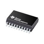
CDC341DW 是德州仪器(Texas Instruments)推出的一款高性能、低偏斜的时钟缓冲器/驱动器,属于CDC系列,采用SOIC-20(DW)封装。其主要应用场景包括:

- 通信基础设施:用于基站、光模块、交换机和路由器中,为FPGA、ASIC、PHY及SerDes等器件提供低抖动、多路同步时钟分配,确保系统时序一致性。

- 工业自动化与测试设备:在高速数据采集系统、PLC、精密仪器中,为ADC/DAC、处理器和逻辑电路提供干净、隔离的时钟信号,降低串扰影响。

- 计算与服务器平台:作为PCIe、DDR内存控制器或CPU外围芯片组的时钟扇出缓冲器,支持1:9 LVCMOS/LVTTL输出,满足多负载同步需求。

- 医疗电子与高端成像设备:在超声、MRI等需高时序精度的系统中,保障图像处理链路中各模块(如FPGA、DSP)的严格相位对齐。

该器件支持宽工作电压(3.0–3.6V),典型输出偏斜<50ps,输入抖动容限高,并具备掉电模式和输出使能控制,便于电源管理与系统同步启动。其无内部PLL的设计也使其适用于需零延迟、确定性传播的纯缓冲场景。
| 参数 | 数值 |
| 产品目录 | 集成电路 (IC)半导体 |
| 描述 | IC CLK BUFFER 1:8 80MHZ 20SOIC时钟驱动器及分配 1-To-8 Clock Driver |
| 产品分类 | |
| 品牌 | Texas Instruments |
| 产品手册 | |
| 产品图片 |
|
| rohs | 符合RoHS无铅 / 符合限制有害物质指令(RoHS)规范要求 |
| 产品系列 | 时钟和计时器IC,时钟驱动器及分配,Texas Instruments CDC341DW- |
| 数据手册 | |
| 产品型号 | CDC341DW |
| 乘法/除法因子 | 1:8 |
| 产品目录页面 | |
| 产品种类 | 时钟驱动器及分配 |
| 供应商器件封装 | 20-SOIC |
| 其它名称 | 296-6701-5 |
| 包装 | 管件 |
| 单位重量 | 500.700 mg |
| 商标 | Texas Instruments |
| 安装类型 | 表面贴装 |
| 安装风格 | SMD/SMT |
| 封装 | Tube |
| 封装/外壳 | 20-SOIC(0.295",7.50mm 宽) |
| 封装/箱体 | SOIC-20 |
| 工作温度 | 0°C ~ 70°C |
| 工厂包装数量 | 25 |
| 差分-输入:输出 | 无/无 |
| 最大功率耗散 | 1600 mW |
| 最大工作温度 | + 70 C |
| 最小工作温度 | 0 C |
| 标准包装 | 25 |
| 比率-输入:输出 | 1:8 |
| 电压-电源 | 4.75 V ~ 5.25 V |
| 电源电压-最大 | 5.25 V |
| 电源电压-最小 | 4.75 V |
| 电源电流 | 2 mA |
| 电路数 | 1 |
| 类型 | 扇出缓冲器(分配) |
| 系列 | CDC341 |
| 输入 | TTL |
| 输出 | TTL |
| 输出类型 | LVTTL |
| 频率-最大值 | 80MHz |


.jpg)


PDF Datasheet 数据手册内容提取
CDC341 1-LINE TO 8-LINE CLOCK DRIVER SCAS333D – DECEMBER 1992 – REVISED OCTOBER 1998 (cid:1) Low Output Skew, Low Pulse Skew for DW PACKAGE Clock-Distribution and Clock-Generation (TOP VIEW) Applications (cid:1) VCC 1 20 VCC TTL-Compatible Inputs and Outputs (cid:1) 1G 2 19 1Y1 Distributes One Clock Input to Eight 2G 3 18 1Y2 Outputs A 4 17 GND (cid:1) Distributed VCC and Ground Pins Reduce P0 5 16 1Y3 Switching Noise P1 6 15 1Y4 (cid:1) High-Drive Outputs (–48-mA IOH, VCC 7 14 GND 48-mA I ) 2Y4 8 13 2Y1 OL (cid:1) State-of-the-Art EPIC-II B BiCMOS Design 2Y3 9 12 2Y2 GND 10 11 GND Significantly Reduces Power Dissipation (cid:1) Packaging Options Include Plastic Small-Outline (DW) Packages description The CDC341 is a high-performance clock-driver circuit that distributes one (A) input signal to eight (Y) outputs with minimum skew for clock distribution. Through the use of the control pins (1G and 2G), the outputs can be placed in a low state regardless of the A input. The propagation delays are adjusted at the factory using the P0 and P1 pins. These pins are not intended for customer use and should be strapped to GND. The CDC341 is characterized for operation from 0°C to 70°C. FUNCTION TABLE INPUTS OUTPUTS 1G 2G A 1Y1–1Y4 2Y1–2Y4 X X L L L L L H L L L H H L H H L H H L H H H H H Please be aware that an important notice concerning availability, standard warranty, and use in critical applications of TexasInstruments semiconductor products and disclaimers thereto appears at the end of this data sheet. EPIC-IIB is a trademark of Texas Instruments Incorporated. PRODUCTION DATA information is current as of publication date. Copyright 1998, Texas Instruments Incorporated Products conform to specifications per the terms of Texas Instruments standard warranty. Production processing does not necessarily include testing of all parameters. POST OFFICE BOX 655303 • DALLAS, TEXAS 75265 1
CDC341 1-LINE TO 8-LINE CLOCK DRIVER SCAS333D – DECEMBER 1992 – REVISED OCTOBER 1998 logic symbol† 2 1G G1 3 2G G2 19 1 1Y1 18 1 1Y2 4 16 A 1 1Y3 15 1 1Y4 13 2 2Y1 12 2 2Y2 9 2 2Y3 8 2 2Y4 †This symbol is in accordance with ANSI/IEEE Std 91-1984 and IEC Publication 617-12. logic diagram (positive logic) 2 1G 19 1Y1 3 2G 18 1Y2 16 1Y3 15 1Y4 4 A 13 2Y1 12 2Y2 9 2Y3 8 2Y4 2 POST OFFICE BOX 655303 • DALLAS, TEXAS 75265
CDC341 1-LINE TO 8-LINE CLOCK DRIVER SCAS333D – DECEMBER 1992 – REVISED OCTOBER 1998 absolute maximum ratings over operating free-air temperature range (unless otherwise noted)† Supply voltage range, V . . . . . . . . . . . . . . . . . . . . . . . . . . . . . . . . . . . . . . . . . . . . . . . . . . . . . . . . . . –0.5 V to 7 V CC Input voltage range, V (see Note 1) . . . . . . . . . . . . . . . . . . . . . . . . . . . . . . . . . . . . . . . . . . . . . . . . . . –0.5 V to 7 V I Voltage range applied to any output in the high state or power-off state, V (see Note 1) . . . . . . . . . . . . . . . . . . . . . . . . . . . . . . . . . . . . . . . . . . . . . . . . . . . . . . . . . . –0.5 V to V + 0.5 V O CC Current into any output in the low state, I . . . . . . . . . . . . . . . . . . . . . . . . . . . . . . . . . . . . . . . . . . . . . . . . . . 96 mA O Input clamp current, IIK (VI < 0) . . . . . . . . . . . . . . . . . . . . . . . . . . . . . . . . . . . . . . . . . . . . . . . . . . . . . . . . . . . –18 mA Maximum power dissipation at T = 55°C (in still air) (see Note 2) . . . . . . . . . . . . . . . . . . . . . . . . . . . . . . . 1.6 W A Storage temperature range, T . . . . . . . . . . . . . . . . . . . . . . . . . . . . . . . . . . . . . . . . . . . . . . . . . . . –65°C to 150°C stg †Stresses beyond those listed under “absolute maximum ratings” may cause permanent damage to the device. These are stress ratings only and functional operation of the device at these or any other conditions beyond those indicated under “recommended operating conditions” is not implied. Exposure to absolute-maximum-rated conditions for extended periods may affect device reliability. NOTES: 1. The input and output negative-voltage ratings may be exceeded if the input and output clamp-current ratings are observed. 2. The maximum package power dissipation is calculated using a junction temperature of 150°C and a board trace length of 750 mils. For more information, refer to the Package Thermal Considerations application note in the ABT Advanced BiCMOS Technology Data Book, literature number SCBD002. recommended operating conditions (see Note 3) MIN MAX UNIT VCC Supply voltage 4.75 5.25 V VIH High-level input voltage 2 V VIL Low-level input voltage 0.8 V VI Input voltage 0 VCC V IOH High-level output current –48 mA IOL Low-level output current 48 mA One output bank loaded 80 ffcllockk IInnppuutt cclloocckk ffrreeqquueennccyy MMHHzz Both output banks loaded 40 TA Operating free-air temperature 0 70 °C NOTE 3: Unused pins (input or I/O) must be held high or low. POST OFFICE BOX 655303 • DALLAS, TEXAS 75265 3
CDC341 1-LINE TO 8-LINE CLOCK DRIVER SCAS333D – DECEMBER 1992 – REVISED OCTOBER 1998 electrical characteristics over recommended operating free-air temperature range (unless otherwise noted) TA = 25°C PPAARRAAMMEETTEERR TTEESSTT CCOONNDDIITTIIOONNSS MMIINN MMAAXX UUNNIITT MIN TYP† MAX VIK VCC = 4.75 V, II = –18 mA –1.2 –1.2 V VCC = 4.75 V, IOH = –3 mA 2.5 2.5 VOH VCC = 5 V, IOH = –3 mA 3 3 V VCC = 4.75 V, IOH = –48 mA 2 2 VOL VCC = 4.75 V, IOL = 48 mA 0.5 V II VCC = 5.25 V, VI = VCC or GND ±1 ±1 m A IO‡ VCC = 5.25 V, VO = 2.5 V –50 –100 –200 –50 –200 mA IICCCC VCCCC = 5.25 V,, IOO = 0,, Outputs high 2 3.5 mmAA VI = VCC or GND Outputs low 24 33 Ci VI = 2.5 V or 0.5 V 3 pF †All typical values are at VCC = 5 V. ‡Not more than one output should be tested at a time, and the duration of the test should not exceed one second. switching characteristics, C = 50 pF (see Figures 1 and 2) L VCC = 5 V, VCC = 4.75 V to 5.25 V, PARAMETER FROM TO TA = 25°C TA = 0°C to 70°C UNIT ((IINNPPUUTT)) ((OOUUTTPPUUTT)) MIN TYP MAX MIN MAX tPLH 3.5 4.5 3.1 4.9 AA YY nnss tPHL 3.5 4.3 3.1 4.9 tPLH 2 3.8 2 4 GG YY nnss tPHL 2 3.8 2 4 tsk(o) 0.3 0.5 0.6 tsk(p) A Y 0.6 0.8 0.9 ns tsk(pr) 1 1 tr A Y 1.5 ns tf A Y 1.5 ns t performance information relative to V and temperature variation (see Note 4) pd CC DtPLH(TA)† Temperature drift of tPLH from 0°C to 70°C –41 ps/10°C DtPHL(TA)† Temperature drift of tPHL from 0°C to 70°C –52 ps/10°C DtPLH(VCC)‡ VCC drift of tPLH from 4.75 V to 5.25 V 28 ps/100 mV DtPHL(VCC)‡§ VCC drift of tPHL from 4.75 V to 5.25 V 20 ps/100 mV †Virtually independent of VCC ‡Virtually independent of temperature NOTE 4: The data extracted is from a wide range of characterization material. 4 POST OFFICE BOX 655303 • DALLAS, TEXAS 75265
CDC341 1-LINE TO 8-LINE CLOCK DRIVER SCAS333D – DECEMBER 1992 – REVISED OCTOBER 1998 PARAMETER MEASUREMENT INFORMATION From Output Under Test CL = 50 pF 500 W (see Note A) LOAD CIRCUIT 3 V Input (see Note B) 1.5 V 1.5 V 0 V tPLH tPHL VOH Output 1.5 V 2 V 1.5 V 0.8 V 0.8 V VOL tr tf VOLTAGE WAVEFORMS PROPAGATION DELAY TIMES NOTES: A. CL includes probe and jig capacitance. B. All input pulses are supplied by generators having the following characteristics: PRR ≤ 10 MHz, ZO = 50 W , tr ≤ 2.5 ns, tf≤ 2.5 ns. Figure 1. Load Circuit and Voltage Waveforms A 1G 2G 1Yn tPLH1 tPHL1 2Yn tPLH2 tPHL2 NOTES: A. Output skew, tsk(o), is calculated as the greater of: – The difference between the fastest and slowest of tPLHn (n = 1, 2) – The difference between the fastest and slowest of tPHLn (n = 1, 2) B. Pulse skew, tsk(p), is calculated as the greater of | tPLHn – tPHLn | (n = 1, 2). C. Process skew, tsk(pr), is calculated as the greater of: – The difference between the fastest and slowest of tPLHn (n = 1, 2) across multiple devices under identical operating conditions – The difference between the fastest and slowest of tPHLn (n = 1, 2) across multiple devices under identical operating conditions Figure 2. Waveforms for Calculation of t , t , t sk(o) sk(p) sk(pr) POST OFFICE BOX 655303 • DALLAS, TEXAS 75265 5
CDC341 1-LINE TO 8-LINE CLOCK DRIVER SCAS333D – DECEMBER 1992 – REVISED OCTOBER 1998 MECHANICAL INFORMATION DW (R-PDSO-G**) PLASTIC SMALL-OUTLINE PACKAGE 16 PIN SHOWN 0.050 (1,27) 0.020 (0,51) 0.010 (0,25) M 0.014 (0,35) 16 9 0.419 (10,65) 0.400 (10,15) 0.299 (7,59) 0.010 (0,25) NOM 0.293 (7,45) Gage Plane 0.010 (0,25) 1 8 0°–8° 0.050 (1,27) A 0.016 (0,40) Seating Plane 0.012 (0,30) 0.004 (0,10) 0.104 (2,65) MAX 0.004 (0,10) PINS ** 16 20 24 DIM 0.410 0.510 0.610 A MAX (10,41) (12,95) (15,49) 0.400 0.500 0.600 A MIN (10,16) (12,70) (15,24) 4040000/D 02/98 NOTES: A. All linear dimensions are in inches (millimeters). B. This drawing is subject to change without notice. C. Body dimensions do not include mold flash or protrusion not to exceed 0.006 (0,15). D. Falls within JEDEC MS-013 6 POST OFFICE BOX 655303 • DALLAS, TEXAS 75265
PACKAGE OPTION ADDENDUM www.ti.com 14-Oct-2008 PACKAGING INFORMATION OrderableDevice Status(1) Package Package Pins Package EcoPlan(2) Lead/BallFinish MSLPeakTemp(3) Type Drawing Qty CDC341DBLE OBSOLETE SSOP DB 20 TBD CallTI CallTI CDC341DW ACTIVE SOIC DW 20 25 Green(RoHS& CUNIPDAU Level-1-260C-UNLIM noSb/Br) CDC341DWG4 ACTIVE SOIC DW 20 25 Green(RoHS& CUNIPDAU Level-1-260C-UNLIM noSb/Br) CDC341DWR ACTIVE SOIC DW 20 2000 Green(RoHS& CUNIPDAU Level-1-260C-UNLIM noSb/Br) CDC341DWRG4 ACTIVE SOIC DW 20 2000 Green(RoHS& CUNIPDAU Level-1-260C-UNLIM noSb/Br) CDC341NSR OBSOLETE SO NS 20 TBD CallTI CallTI CDC341NSRG4 OBSOLETE SO NS 20 TBD CallTI CallTI (1)Themarketingstatusvaluesaredefinedasfollows: ACTIVE:Productdevicerecommendedfornewdesigns. LIFEBUY:TIhasannouncedthatthedevicewillbediscontinued,andalifetime-buyperiodisineffect. NRND:Notrecommendedfornewdesigns.Deviceisinproductiontosupportexistingcustomers,butTIdoesnotrecommendusingthispartin anewdesign. PREVIEW:Devicehasbeenannouncedbutisnotinproduction.Samplesmayormaynotbeavailable. OBSOLETE:TIhasdiscontinuedtheproductionofthedevice. (2)EcoPlan-Theplannedeco-friendlyclassification:Pb-Free(RoHS),Pb-Free(RoHSExempt),orGreen(RoHS&noSb/Br)-pleasecheck http://www.ti.com/productcontentforthelatestavailabilityinformationandadditionalproductcontentdetails. TBD:ThePb-Free/Greenconversionplanhasnotbeendefined. Pb-Free(RoHS):TI'sterms"Lead-Free"or"Pb-Free"meansemiconductorproductsthatarecompatiblewiththecurrentRoHSrequirements forall6substances,includingtherequirementthatleadnotexceed0.1%byweightinhomogeneousmaterials.Wheredesignedtobesoldered athightemperatures,TIPb-Freeproductsaresuitableforuseinspecifiedlead-freeprocesses. Pb-Free(RoHSExempt):ThiscomponenthasaRoHSexemptionforeither1)lead-basedflip-chipsolderbumpsusedbetweenthedieand package, or 2) lead-based die adhesive used between the die and leadframe. The component is otherwise considered Pb-Free (RoHS compatible)asdefinedabove. Green(RoHS&noSb/Br):TIdefines"Green"tomeanPb-Free(RoHScompatible),andfreeofBromine(Br)andAntimony(Sb)basedflame retardants(BrorSbdonotexceed0.1%byweightinhomogeneousmaterial) (3) MSL, Peak Temp. -- The Moisture Sensitivity Level rating according to the JEDEC industry standard classifications, and peak solder temperature. Important Information and Disclaimer:The information provided on this page represents TI's knowledge and belief as of the date that it is provided. TI bases its knowledge and belief on information provided by third parties, and makes no representation or warranty as to the accuracy of such information. Efforts are underway to better integrate information from third parties. TI has taken and continues to take reasonable steps to provide representative and accurate information but may not have conducted destructive testing or chemical analysis on incomingmaterialsandchemicals.TIandTIsuppliersconsidercertaininformationtobeproprietary,andthusCASnumbersandotherlimited informationmaynotbeavailableforrelease. InnoeventshallTI'sliabilityarisingoutofsuchinformationexceedthetotalpurchasepriceoftheTIpart(s)atissueinthisdocumentsoldbyTI toCustomeronanannualbasis. Addendum-Page1
PACKAGE MATERIALS INFORMATION www.ti.com 11-Mar-2008 TAPE AND REEL INFORMATION *Alldimensionsarenominal Device Package Package Pins SPQ Reel Reel A0(mm) B0(mm) K0(mm) P1 W Pin1 Type Drawing Diameter Width (mm) (mm) Quadrant (mm) W1(mm) CDC341DWR SOIC DW 20 2000 330.0 24.4 10.8 13.0 2.7 12.0 24.0 Q1 PackMaterials-Page1
PACKAGE MATERIALS INFORMATION www.ti.com 11-Mar-2008 *Alldimensionsarenominal Device PackageType PackageDrawing Pins SPQ Length(mm) Width(mm) Height(mm) CDC341DWR SOIC DW 20 2000 346.0 346.0 41.0 PackMaterials-Page2
IMPORTANTNOTICE TexasInstrumentsIncorporatedanditssubsidiaries(TI)reservetherighttomakecorrections,modifications,enhancements,improvements, andotherchangestoitsproductsandservicesatanytimeandtodiscontinueanyproductorservicewithoutnotice.Customersshould obtainthelatestrelevantinformationbeforeplacingordersandshouldverifythatsuchinformationiscurrentandcomplete.Allproductsare soldsubjecttoTI’stermsandconditionsofsalesuppliedatthetimeoforderacknowledgment. TIwarrantsperformanceofitshardwareproductstothespecificationsapplicableatthetimeofsaleinaccordancewithTI’sstandard warranty.TestingandotherqualitycontroltechniquesareusedtotheextentTIdeemsnecessarytosupportthiswarranty.Exceptwhere mandatedbygovernmentrequirements,testingofallparametersofeachproductisnotnecessarilyperformed. TIassumesnoliabilityforapplicationsassistanceorcustomerproductdesign.Customersareresponsiblefortheirproductsand applicationsusingTIcomponents.Tominimizetherisksassociatedwithcustomerproductsandapplications,customersshouldprovide adequatedesignandoperatingsafeguards. TIdoesnotwarrantorrepresentthatanylicense,eitherexpressorimplied,isgrantedunderanyTIpatentright,copyright,maskworkright, orotherTIintellectualpropertyrightrelatingtoanycombination,machine,orprocessinwhichTIproductsorservicesareused.Information publishedbyTIregardingthird-partyproductsorservicesdoesnotconstitutealicensefromTItousesuchproductsorservicesora warrantyorendorsementthereof.Useofsuchinformationmayrequirealicensefromathirdpartyunderthepatentsorotherintellectual propertyofthethirdparty,oralicensefromTIunderthepatentsorotherintellectualpropertyofTI. ReproductionofTIinformationinTIdatabooksordatasheetsispermissibleonlyifreproductioniswithoutalterationandisaccompanied byallassociatedwarranties,conditions,limitations,andnotices.Reproductionofthisinformationwithalterationisanunfairanddeceptive businesspractice.TIisnotresponsibleorliableforsuchaltereddocumentation.Informationofthirdpartiesmaybesubjecttoadditional restrictions. ResaleofTIproductsorserviceswithstatementsdifferentfromorbeyondtheparametersstatedbyTIforthatproductorservicevoidsall expressandanyimpliedwarrantiesfortheassociatedTIproductorserviceandisanunfairanddeceptivebusinesspractice.TIisnot responsibleorliableforanysuchstatements. TIproductsarenotauthorizedforuseinsafety-criticalapplications(suchaslifesupport)whereafailureoftheTIproductwouldreasonably beexpectedtocauseseverepersonalinjuryordeath,unlessofficersofthepartieshaveexecutedanagreementspecificallygoverning suchuse.Buyersrepresentthattheyhaveallnecessaryexpertiseinthesafetyandregulatoryramificationsoftheirapplications,and acknowledgeandagreethattheyaresolelyresponsibleforalllegal,regulatoryandsafety-relatedrequirementsconcerningtheirproducts andanyuseofTIproductsinsuchsafety-criticalapplications,notwithstandinganyapplications-relatedinformationorsupportthatmaybe providedbyTI.Further,BuyersmustfullyindemnifyTIanditsrepresentativesagainstanydamagesarisingoutoftheuseofTIproductsin suchsafety-criticalapplications. TIproductsareneitherdesignednorintendedforuseinmilitary/aerospaceapplicationsorenvironmentsunlesstheTIproductsare specificallydesignatedbyTIasmilitary-gradeor"enhancedplastic."OnlyproductsdesignatedbyTIasmilitary-grademeetmilitary specifications.BuyersacknowledgeandagreethatanysuchuseofTIproductswhichTIhasnotdesignatedasmilitary-gradeissolelyat theBuyer'srisk,andthattheyaresolelyresponsibleforcompliancewithalllegalandregulatoryrequirementsinconnectionwithsuchuse. TIproductsareneitherdesignednorintendedforuseinautomotiveapplicationsorenvironmentsunlessthespecificTIproductsare designatedbyTIascompliantwithISO/TS16949requirements.Buyersacknowledgeandagreethat,iftheyuseanynon-designated productsinautomotiveapplications,TIwillnotberesponsibleforanyfailuretomeetsuchrequirements. FollowingareURLswhereyoucanobtaininformationonotherTexasInstrumentsproductsandapplicationsolutions: Products Applications Amplifiers amplifier.ti.com Audio www.ti.com/audio DataConverters dataconverter.ti.com Automotive www.ti.com/automotive DSP dsp.ti.com Broadband www.ti.com/broadband ClocksandTimers www.ti.com/clocks DigitalControl www.ti.com/digitalcontrol Interface interface.ti.com Medical www.ti.com/medical Logic logic.ti.com Military www.ti.com/military PowerMgmt power.ti.com OpticalNetworking www.ti.com/opticalnetwork Microcontrollers microcontroller.ti.com Security www.ti.com/security RFID www.ti-rfid.com Telephony www.ti.com/telephony RF/IFandZigBee®Solutions www.ti.com/lprf Video&Imaging www.ti.com/video Wireless www.ti.com/wireless MailingAddress:TexasInstruments,PostOfficeBox655303,Dallas,Texas75265 Copyright©2008,TexasInstrumentsIncorporated