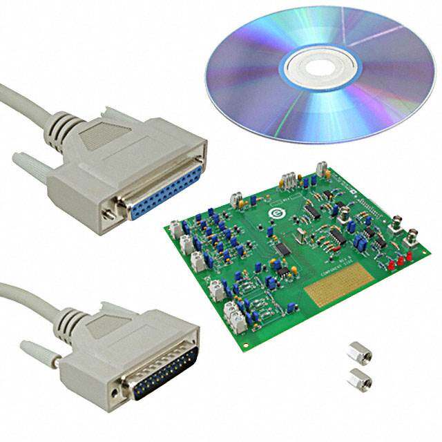
ICGOO在线商城 > 开发板,套件,编程器 > 评估和演示板和套件 > CDB8422

 Datasheet下载
- 型号: CDB8422
- 制造商: Cirrus Logic
- 库位|库存: xxxx|xxxx
- 要求:
| 数量阶梯 | 香港交货 | 国内含税 |
| +xxxx | $xxxx | ¥xxxx |
查看当月历史价格
查看今年历史价格
CDB8422产品简介:
ICGOO电子元器件商城为您提供CDB8422由Cirrus Logic设计生产,在icgoo商城现货销售,并且可以通过原厂、代理商等渠道进行代购。 CDB8422价格参考。Cirrus LogicCDB8422封装/规格:评估和演示板和套件, CS8422 Sample Rate Converter Audio Evaluation Board。您可以下载CDB8422参考资料、Datasheet数据手册功能说明书,资料中有CDB8422 详细功能的应用电路图电压和使用方法及教程。
Cirrus Logic Inc. 的型号 CDB8422 是一款评估和演示板,主要用于支持 Cirrus Logic 的 CS4222 音频编解码器芯片。以下是其主要应用场景:

1. 音频设备开发:CDB8422 提供了一个完整的硬件平台,用于评估 CS4222 编解码器在各种音频应用中的性能。它适用于开发家庭音频设备(如音响、条形音箱)以及便携式音频设备(如耳机放大器、便携式扬声器)。

2. 高保真音频测试:CS4222 支持高达 24 位/192 kHz 的音频分辨率,因此 CDB8422 可用于测试和验证高保真音频信号的处理能力,包括低失真、低噪声的音频输出。

3. 数字音频接口测试:该板支持多种数字音频接口(如 I2S、TDM、SPDIF 等),可用于测试不同设备之间的数字音频传输兼容性,例如与 DSP、MCU 或其他音频处理器的连接。

4. 语音处理应用:CDB8422 可用于开发需要高质量麦克风输入的应用场景,例如语音识别、语音增强或会议系统。CS4222 的高性能 ADC 和 DAC 能够提供清晰的语音采集和播放。

5. 教育和研究:对于音频工程或电子工程领域的学生和研究人员,CDB8422 是一个理想的工具,可以用来学习和实验音频信号处理技术、数字音频协议以及音频编解码器的工作原理。

6. 原型设计和验证:开发人员可以使用 CDB8422 快速构建原型,验证设计概念,并优化音频系统的性能参数,从而加快产品开发周期。

总之,CDB8422 主要用于评估和开发基于 CS4222 编解码器的音频解决方案,适合需要高音质和多功能音频接口的各种应用场景。
| 参数 | 数值 |
| 产品目录 | 编程器,开发系统 |
| 描述 | BOARD EVAL FOR CS8422 RCVR |
| 产品分类 | |
| 品牌 | Cirrus Logic Inc |
| 数据手册 | |
| 产品图片 | |
| 产品型号 | CDB8422 |
| rohs | 含铅 / 不符合限制有害物质指令(RoHS)规范要求 |
| 产品系列 | - |
| 主要属性 | PCM,IEC-60958,AES3/EBU,S/PDIF,以及 XLR 输入,RCA 同轴和光学 S/PDIF 输出 |
| 主要用途 | 音频,采样率转换器 |
| 产品目录页面 | |
| 使用的IC/零件 | CS8422 |
| 其它名称 | 598-1568 |
| 嵌入式 | 是,FPGA / CPLD |
| 所含物品 | 板 |
| 标准包装 | 1 |
| 相关产品 | /product-detail/zh/CS8422-CNZ/598-1732-ND/2024929 |
| 辅助属性 | 28 ~ 216 kHz 采样率范围,输入/输出率范围从 6:1 至 1:6 |


- 商务部:美国ITC正式对集成电路等产品启动337调查
- 曝三星4nm工艺存在良率问题 高通将骁龙8 Gen1或转产台积电
- 太阳诱电将投资9.5亿元在常州建新厂生产MLCC 预计2023年完工
- 英特尔发布欧洲新工厂建设计划 深化IDM 2.0 战略
- 台积电先进制程称霸业界 有大客户加持明年业绩稳了
- 达到5530亿美元!SIA预计今年全球半导体销售额将创下新高
- 英特尔拟将自动驾驶子公司Mobileye上市 估值或超500亿美元
- 三星加码芯片和SET,合并消费电子和移动部门,撤换高东真等 CEO
- 三星电子宣布重大人事变动 还合并消费电子和移动部门
- 海关总署:前11个月进口集成电路产品价值2.52万亿元 增长14.8%


PDF Datasheet 数据手册内容提取
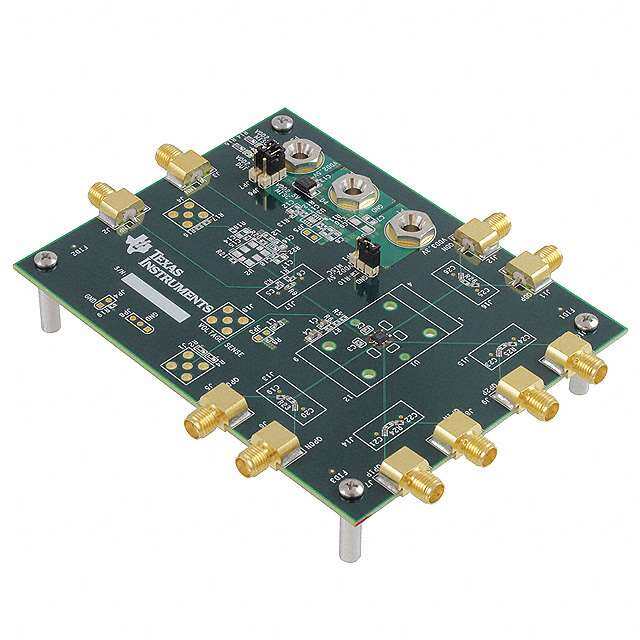
CDB8422 Evaluation Board for CS8422 Features Description IEC-60958, AES3/EBU, S/PDIF Inputs Using the CDB8422 evaluation board is an ideal way to evaluate the CS8422. Use of the board requires a digital – Single-Ended Inputs via Optical and RCA signal source, an analyzer, and a power supply. A Win- Input Jacks dows PC-compatible computer is also required if using – Differential Inputs via XLR Input Jack software mode to configure the CDB8422. S/PDIF Outputs S/PDIF and AES3/EBU input connections are made via RCA phono, optical, or XLR connectors to the CS8422. – Optical and RCA Output Jacks S/PDIF output connections are made via RCA phono or – CS8406 Digital Audio Transmitter optical connectors from the CS8406 (S/PDIF Tx). Sys- tem timing can be provided by a S/PDIF or AES3/EBU I/O Stake Headers input signal, by the CS8422 with supplied master clock, – External Control Port Accessibility or by an I/O stake header with a DSP connected. – External Serial Audio I/O Accessibility The provided Windows-based software GUI makes configuring the CDB8422 easy. The software communi- 3.3 V Logic Interface cates through the PC’s USB port to configure the board so that all features of the CS8422 can be evaluated. Powered by Single External Power Supply or The board may also be configured without a PC con- PC USB Port Connection nection by using hardware switches; however, not all configurations of the CDB8422 are possible in hard- H/W Control via DIP Switches ware mode. FlexGUI S/W Control - Windows® Compatible ORDERING INFORMATION – Pre-Defined & User-Configurable Scripts CDB8422 Evaluation Board Crystal Canned Oscillator Oscillator Canned Jumper XTI Reset RMCK Mux Oscillator OMCK OSCLK1 er ISCLK ader IILSRCCLKK OSDLROCUKT11 Head ILSRDCINK CS8406 TX Output e H SDIN CS8422 OSCLK2 er RX Input d OLRCK2 a e H SDOUT2 TDM_IN der a e H USB Micro- USB I2C/SPI controller Resistors FPGA Hardware Reset Switches Copyright Cirrus Logic, Inc. 2010 MAY '10 http://www.cirrus.com (All Rights Reserved) DS692DB2
CDB8422 TABLE OF CONTENTS 1. SYSTEM OVERVIEW .............................................................................................................................4 1.1 Power ...............................................................................................................................................4 1.2 Grounding and Power Supply Decoupling .......................................................................................4 1.3 FPGA ...............................................................................................................................................4 1.4 CS8422 ............................................................................................................................................4 1.5 CS8406 Digital Audio Transmitter ....................................................................................................5 1.6 CS8422 XTI Sources .......................................................................................................................5 1.7 I/O Stake Headers ...........................................................................................................................5 1.8 S/PDIF and AES3/EBU Inputs .........................................................................................................5 2. SOFTWARE MODE ................................................................................................................................6 2.1 Quick Start Guide .............................................................................................................................6 2.2 Configuration Options ......................................................................................................................7 2.2.1 S/PDIF In to S/PDIF and PCM Out .........................................................................................7 2.2.2 AES3/EBU In to S/PDIF and PCM Out ...................................................................................8 2.2.3 PCM In to S/PDIF and PCM Out .............................................................................................9 2.2.4 TDM In to TDM Out ...............................................................................................................10 2.3 Software Mode Control ..................................................................................................................11 2.3.1 CS8422 Main Setup Tab .......................................................................................................12 2.3.2 CS8422 Receiver Controls and Status Tab ..........................................................................13 2.3.3 CS8422 Interrupt Controls and Status Tab ...........................................................................14 2.3.4 FPGA Controls Tab ...............................................................................................................15 2.3.5 Register Maps Tab ................................................................................................................16 2.4 FPGA Register Quick Reference ...................................................................................................17 2.5 FPGA Register Descriptions ..........................................................................................................17 2.5.1 Code Revision ID (Address 01h) - Read Only .......................................................................17 2.5.2 MCLK Control (Address 02h) ................................................................................................17 2.5.2.1 SAO2 HDR MCLK Source (SAO2_Mclk) ...................................................................17 2.5.2.2 SAO1 HDR and CS8406 MCLK Source (SAO1_Mclk) ..............................................17 2.5.2.3 AUX MCLK Source (AUX_Mclk) ................................................................................18 2.5.2.4 CS8422 Reset Pin (DUT_RST) .................................................................................18 2.5.3 Subclock Control (Address 03h) ............................................................................................18 2.5.3.1 TDM Header Subclock Source (TDM_SEL) ..............................................................18 2.5.3.2 SAI Subclock Source (SAI_MS) ................................................................................18 2.5.3.3 SAO2 Subclock Source (SAO2_MS) .........................................................................19 2.5.3.4 SAO1 Subclock Source (SAO1_MS) .........................................................................19 2.5.4 CS8406 Control 1 (Address 04h) ..........................................................................................19 2.5.4.1 OMCK/ILRCK Ratio (HWCK) .....................................................................................19 2.5.4.2 Validity Bit (VBIT_IN) .................................................................................................19 2.5.4.3 User Data (UBIT_IN) .................................................................................................20 2.5.4.4 TCBL (TCBL) .............................................................................................................20 2.5.4.5 C BIT (CBIT_INT) ......................................................................................................20 2.5.4.6 Interface Format (SFMT) ...........................................................................................20 2.5.5 CS8406 Control 2 (Address 05h) ..........................................................................................21 2.5.5.1 CS8406 Reset Pin (8406_RST) .................................................................................21 2.5.5.2 AUDIO Bit (AUDIOb) .................................................................................................21 3. HARDWARE MODE .............................................................................................................................22 3.1 Quick Start Guide ...........................................................................................................................22 3.2 Configuration Options ....................................................................................................................23 3.2.1 AES3/EBU In to S/PDIF and PCM Out .................................................................................23 3.2.2 TDM In to TDM Out ...............................................................................................................24 3.3 Hardware Mode Control .................................................................................................................25 4. SYSTEM CONNECTIONS ...................................................................................................................28 2 DS692DB2
CDB8422 5. JUMPER SETTINGS ...........................................................................................................................29 6. LEDS ....................................................................................................................................................29 7. CDB8422 BLOCK DIAGRAM ..............................................................................................................30 8. CDB8422 SCHEMATICS ......................................................................................................................31 9. CDB8422 LAYOUT ...............................................................................................................................43 10. REVISION HISTORY ..........................................................................................................................46 LIST OF FIGURES Figure 1.Software Mode Quick Start Guide ................................................................................................6 Figure 2.S/PDIF In to S/PDIF and PCM Out ...............................................................................................7 Figure 3.AES3/EBU In to S/PDIF and PCM Out .........................................................................................8 Figure 4.PCM In to S/PDIF and PCM Out ...................................................................................................9 Figure 5.TDM In to TDM Out .....................................................................................................................10 Figure 6.CS8422 Main Setup Tab .............................................................................................................12 Figure 7.CS8422 Receiver Controls and Status Tab ................................................................................13 Figure 8.CS8422 Interrupt Controls and Status Tab .................................................................................14 Figure 9.FPGA Controls Tab .....................................................................................................................15 Figure 10.Register Maps Tab - CS8422 ...................................................................................................16 Figure 11.Hardware Mode Quick Start Guide ...........................................................................................22 Figure 12.AES3/EBU In to S/PDIF and PCM Out .....................................................................................23 Figure 13.TDM In to TDM Out ...................................................................................................................24 Figure 14.Block Diagram ...........................................................................................................................30 Figure 15.CS8422 & XTI (Schematic Sheet 1) .........................................................................................31 Figure 16.RX Inputs (Schematic Sheet 2) .................................................................................................32 Figure 17.PCM Input Header (Schematic Sheet 3) ...................................................................................33 Figure 18.HW Mode Control (Schematic Sheet 4) ....................................................................................34 Figure 19.FPGA (Schematic Sheet 5) .......................................................................................................35 Figure 20.MCLK Routing (Schematic Sheet 6) .........................................................................................36 Figure 21.Serial Audio 1 Output Header (Schematic Sheet 7) .................................................................37 Figure 22.Serial Audio 2 Output Header (Schematic Sheet 8) .................................................................38 Figure 23.TDM Header (Schematic Sheet 9) ............................................................................................39 Figure 24.CS8406 and Auxiliary TX (Schematic Sheet 10) ......................................................................40 Figure 25.USB and MCU (Schematic Sheet 11) .......................................................................................41 Figure 26.Power (Schematic Sheet 12) ....................................................................................................42 Figure 27.Silk Screen ................................................................................................................................43 Figure 28.Top-Side Layer .........................................................................................................................44 Figure 29.Bottom-Side Layer ....................................................................................................................45 LIST OF TABLES Table 1. Switch Settings - AES3/EBU In to S/PDIF and PCM Out ...........................................................23 Table 2. Switch Settings - TDM In to TDM Out .........................................................................................24 Table 3. S3 Settings ..................................................................................................................................25 Table 4. S4 Settings ..................................................................................................................................26 Table 5. S7 Settings ..................................................................................................................................27 Table 6. System Connections ...................................................................................................................28 Table 7. Jumper Settings ..........................................................................................................................29 Table 8. LEDs ...........................................................................................................................................29 DS692DB2 3
CDB8422 1. SYSTEM OVERVIEW The CDB8422 platform provides S/PDIF and AES3/EBU digital interfaces to the CS8422 and allows for external DSP and I²C® or SPITM control port interconnects. On-board voltage regulators are provided so that a single external power supply of +5V can be used to provide power for the CDB8422. Optionally, the evaluation board may be pow- ered from a USB connection, which also serves as an interface to a PC. The CDB8422 is configured in software mode using Cirrus Logic’s Windows-compatible FlexGUI software to read/write to device registers. In hardware mode, the evaluation board is configured using several DIP switches. This section describes the various components on the CDB8422 and how they are used. The two following sections (Section 2 and Section 3) provide details on operating the CDB8422 in software and hardware mode, respectively. Both sections begin with a simplified quick connect guide provided for user convenience which can be used to set up the board quickly with the CS8422 in its startup default configuration. Next, descriptions are given for several useful configuration options in which the board can be used. Then, complete configuration details for each mode are described. Section 4, Section 5, and Section 6 provide a description of all stake headers, connectors, and LEDs on the board, including the default factory settings for all jumpers. The CDB8422 schematic and layout set is shown in Figures15 through 29. 1.1 Power Power and ground is supplied to the evaluation board via binding posts J2 and J3 (respectively) or the USB connection J37. Jumper J20 allows the user to select the power source (see Section 5 for details). The volt- age connected to the binding posts should be +5V. An on-board voltage regulator provides +3.3V for the CS8422’s VA, VL, and V_REG supplies. All voltage inputs are referenced to ground using the black binding post J3. 1.2 Grounding and Power Supply Decoupling The CDB8422 demonstrates the optimal power supply and grounding arrangements for the CS8422. Figure14 provides an overview of the connections to the CS8422. Figure27 shows the component place- ment, Figure28 shows the top layout, and Figure29 shows the bottom layout. Power supply decoupling ca- pacitors are located as close as possible to the CS8422. Extensive use of ground plane fill helps reduce radiated noise. 1.3 FPGA The FPGA controls digital signal routing between the CS8422, the CS8406, and the I/O stake headers. It also provides routing control of the system master clock from an on-board canned oscillator, an on-board crystal oscillator, and the CS8422. The FPGA configures the CDB8422 in hardware mode and routes serial control signals from the micro controller to the CS8422 in software mode. The Cirrus FlexGUI software pro- vides full control of the FPGA’s routing and configuration options, see Section 2.3, Section 2.4, and Section 2.5 for details. A subset of the FPGA’s options are accessible in hardware mode using DIP switches, see Section 3.3 for details. 1.4 CS8422 A complete description of the CS8422 can be found in the CS8422 product data sheet. When the evaluation board is connected to a PC via the USB connector, the CS8422 is placed in software mode and is configured using the Cirrus FlexGUI. The device configuration registers are accessible via the “Register Maps” tab of the Cirrus FlexGUI software. This tab provides low-level control of each bit. For eas- ier configuration, additional tabs provide high-level control. Section 2.3 provides configuration details. 4 DS692DB2
CDB8422 When the evaluation board is not connected to a PC, the CS8422 is placed in hardware mode and is con- figured using DIP switches. Certain switch settings require a board reset to take affect, see Section 3.3 for more information. 1.5 CS8406 Digital Audio Transmitter A complete description of the CS8406 transmitter and a discussion of the digital audio interface can be found in the CS8406 data sheet. The CS8406 converts the output PCM data stream from the CS8422 into S/PDIF data that is output to the optical (J28) and RCA (J27) connectors. In software mode, device configuration pins are controlled by using the “FPGA Controls” tab of the Cirrus FlexGUI software, see Section 2.3 for details. 1.6 CS8422 XTI Sources The CS8422 XTI clock source is selected by jumper J23. The clock signal may be provided by the socketed on-board canned oscillator (Y1), socketed on-board parallel resonant crystal (Y2), or input serial header J22. The oscillator and crystal are mounted in pin sockets, allowing for easy removal and replacement. The device footprint on the board for Y1 will only accommodate half-can-sized oscillators. Section 5 describes which jumper position selects each clock source. 1.7 I/O Stake Headers The evaluation board has been designed to allow interfacing with external systems via several serial port headers and a control port header (J26). The input serial port header (J22) provides access to the input se- rial audio port of the CS8422. The output serial port headers provide access to both output serial audio port1 (J24) and output serial audio port2 (J25) of the CS8422. All three serial port headers can be placed in master or slave mode with respect to the CS8422. The TDM input header (J30) allows TDM data to be input from another system into the CS8422. The control port header provides bidirectional access to the I²C or SPI control port signals by simply remov- ing all the shunts from the “PC Control” position. The user may then connect a ribbon cable connector to the “External Connection” pins for external control of board functions. A single row of “GND” pins is provided to maintain signal ground integrity. Two unpopulated pull-up resistors are also available should the user choose to use the CDB8422 logic supply (VL) externally. 1.8 S/PDIF and AES3/EBU Inputs The CDB8422 allows for both S/PDIF and AES3/EBU input signals to be connected to the CS8422. Four pairs of optical and RCA connectors are provided to connect single-ended S/PDIF signals to the four receiv- er ports on the CS8422. A single XLR connector is provided to connect a differential AES3/EBU signal to either of the two differential receiver ports on the CS8422. Figure16 illustrates how the S/PDIF and AES3/EBU inputs are connected and routed. Table7 details the associated jumper selections. The CS8422 data sheet specifies the maximum allowed input voltage levels. Note that, as a result of signal attenuation resulting from PCB parasitics, the input S/PDIF signal amplitude at the receiver input pins of the CS8422 may be lower than at the input connectors. See the CS8422 data sheet for the minimum signal amplitude required at the receiver input pins of the CS8422. DS692DB2 5
CDB8422 2. SOFTWARE MODE Connecting a USB port cable from a PC to the USB connector (J37) on the CDB8422 and launching the provided graphical user interface (Cirrus Logic FlexGUI) software enables one to use the board in software mode. The GUI for the CDB8422 allows the user to configure the CS8422 and FPGA registers via the on-board I²C or SPI control bus. 2.1 Quick Start Guide Figure1 below is a simplified quick start up guide made for user convenience. The user may choose from steps 8 through 13 depending on the desired measurement. Refer to Section 2.2 for details on how the var- ious components on the board interface with each other in different board configurations. Refer to Section 2.3 for descriptions on control settings in the Cirrus FlexGUI software. TDM input can be Shunt right 2 pins of J20 provided to the board via PCM digital audio output can be to receive power from 1 header J30. 13 received from the board via USB +5 V DC power. headers J24 and J25. Connect USB to board. 11 Open Flex GUI software PCM digital audio on PC and load quick input can be provided setup script. to the board via *See section 2.2 for header J22. quick setup descriptions. 10 7 Shunt the middle 2 pins on J23. 2 Shunt the top 2 pins on J21 and J29. 3 Provide S/PDIF input to board via 12 J1 or J7. 8 Receive S/PDIF output from board via J28 or J27. Shunt top 2 pins on J4 5 4 9 6 if using optical input J1. Shunt bottom 2 AES3/EBU input Shunt the right 2 pins on all rows. Shunt the top 2 pins pins on J4 if using can also be Connect a ribbon cable to left 2 on J31. coaxial input J7. provided to the pins of all rows if external system connect is required. board via J19. Figure 1. Software Mode Quick Start Guide 6 DS692DB2
CDB8422 2.2 Configuration Options In software mode, to configure the CDB8422 for making performance measurements, one needs to use Cir- rus Logic’s Windows compatible FlexGUI software to program the various components on the board. This section serves to give a deeper understanding of the on-board circuitry and the digital clock and data signal routing involved in several common software mode configurations of the CDB8422. These scripts only serve as a starting point; after loading a script, the GUI can be further configured as needed (clock ratios, serial formats, etc). 2.2.1 S/PDIF In to S/PDIF and PCM Out The CS8422’s S/PDIF receiver and SRC output performance can be tested by loading the “SPDIF In to SPDIF and PCM Out” quick setup file provided with the software package. The script configures the dig- ital clock and data signal routing on the board as shown in Figure2. Digital S/PDIF input can be provided on the optical (J1) or RCA (J7) jacks. Jumper J4 selects which input signal is connected to the RX0 pin of the CS8422. The script configures the CS8422’s internal circuitry to send the input audio data through its SRC to serial output port 1. This data is presented as PCM audio at header J24 and S/PDIF audio at J27 (coaxial) and J28 (optical). The input data is also passed through (SRC is bypassed) to serial output port 2. This data is presented as PCM audio at header J25. Refer to Section 2.3 for details on software configuration. Header J24 OSCLK1 PCM Out OLRCK1 through SRC SDOUT1 MCLK OUT Optical J28 S/PDIF Buffer Buffer CS8406 Out S/PDIF Tx Optical OSCLK1 ISCLK S/PDIF J1 (MASTER)OLRCK1 ILRCK(SLAVE) OUT AND S/PDIF In SDOUT1 SDIN J31 OMCK Coaxial OR J4 RX0 CS8422 RMCK J27 S/PDIF Buffer Header Out J25 Coaxial MCLK OUT PCM Out J7 S/PDIF In OSCLK2 OSCLK2 no SRC (MASTER)OLRCK2 OLRCK2 SDOUT2 SDOUT2 Figure 2. S/PDIF In to S/PDIF and PCM Out DS692DB2 7
CDB8422 2.2.2 AES3/EBU In to S/PDIF and PCM Out The CS8422’s AES3/EBU receiver and SRC output performance can be tested by loading the “AES3 In to SPDIF and PCM Out” quick setup file provided with the software package. The script configures the digital clock and data signal routing on the board as shown in Figure3. Digital AES3/EBU input is provided by the XLR jack J19 to the RXP0 and RXN0 pins of the CS8422. The script configures the CS8422’s internal circuitry to send the input audio data through its SRC to serial out- put port 1. This data is presented as PCM audio at header J24 and S/PDIF audio at J27 (coaxial) and J28 (optical). The input data is also passed through (SRC is bypassed) to serial output port 2. This data is presented as PCM audio at header J25. Refer to Section 2.3 for details on software configuration. Header J24 OSCLK1 PCM Out OLRCK1 through SRC SDOUT1 MCLK OUT Optical J28 S/PDIF Buffer Buffer CS8406 Out S/PDIF Tx OSCLK1 ISCLK S/PDIF (MASTER)OLRCK1 ILRCK(SLAVE) OUT AND SDOUT1 SDIN J31 J21 OMCK RXP0 Coaxial AES3/EBU RXP1 J19 CS8422 RMCK J27 S/PDIF In RRXXNN01 Buffer Header Out J29 J25 MCLK OUT PCM Out OSCLK2 OSCLK2 no SRC (MASTER)OLRCK2 OLRCK2 SDOUT2 SDOUT2 Figure 3. AES3/EBU In to S/PDIF and PCM Out 8 DS692DB2
CDB8422 2.2.3 PCM In to S/PDIF and PCM Out The CS8422’s serial input port and SRC output performance can be tested by loading the “PCM In to SPDIF and PCM Out” quick setup file provided with the software package. The script configures the dig- ital clock and data signal routing on the board as shown in Figure4. PCM audio input is provided by the PCM input header J22. The jumper position on J23 may be changed to use the MCLK signal from J22 for the CS8422’s XTI signal. The script configures the CS8422’s internal circuitry to send the input audio data through its SRC to serial output port 1. This data is presented as PCM audio at header J24 and S/PDIF audio at J27 (coaxial) and J28 (optical). The input data is also passed through (SRC is bypassed) to serial output port 2. This data is presented as PCM audio at header J25. Refer to Section 2.3 for details on software configuration. Header J24 Y1 OSCLK1 PCM Out OLRCK1 through SRC SDOUT1 J23 MCLK OUT Optical J28 S/PDIF XTI Buffer Buffer CS8406 Out S/PDIF Tx PCM In OSCLK1 ISCLK S/PDIF Header Buffer (MASTER)OLRCK1 ILRCK(SLAVE) OUT AND J22 SDOUT1 SDIN J31 CS8422 OMCK MCLK Coaxial ISCLK ISCLK ILRCK ILRCK(SLAVE) RMCK J27 S/PDIF SDIN SDIN Buffer Header Out J25 MCLK OUT PCM Out OSCLK2 OSCLK2 no SRC (MASTER)OLRCK2 OLRCK2 SDOUT2 SDOUT2 Figure 4. PCM In to S/PDIF and PCM Out DS692DB2 9
CDB8422 2.2.4 TDM In to TDM Out The CS8422’s TDM output performance can be tested by loading the “TDM In to TDM Out” quick setup file provided with the software package. The script configures the digital clock and data signal routing on the board as shown in Figure5. TDM audio input data is provided by the TDM input header J30. The LRCK and SCLK signals located at header J30 should be used to clock in the input TDM data. Optionally, digital S/PDIF input can be provided on the optical (J1) or RCA (J7) jacks. Jumper J4 selects which input signal is connected to the RX0 pin of the CS8422. The script configures the CS8422’s internal circuitry to multiplex the TDM input and S/PDIF input data together and send the output data to serial output port 1. This data is presented as TDM audio at header J24. The S/PDIF input data is also passed through (not multiplexed) to serial output port 2. This data is presented as PCM audio at header J25. Refer to Section 2.3 for details on software configuration. Header Buffer J30 Y1 TDM IN TDM TDM In OSCLK TDM J23 OLRCK XTI TDM_IN Buffer Header J24 OSCLK1 OSCLK1 Optical TDM J1 (MASTER)OLRCK1 OLRCK1 S/PDIF In Out SDOUT1 SDOUT1 GPO3 MCLK OUT (XTI) OR J4 RX0 CS8422 Header Buffer J25 Coaxial RMCK MCLK OUT PCM Out J7 S/PDIF In OSCLK2 OSCLK2 no SRC (MASTER)OLRCK2 OLRCK2 SDOUT2 SDOUT2 Figure 5. TDM In to TDM Out 10 DS692DB2
CDB8422 2.3 Software Mode Control The CDB8422 may be used with the Microsoft® Windows®-based FlexGUI graphical user interface, allow- ing software control of the CS8422 and FPGA registers. The latest control software may be downloaded from www.cirrus.com/msasoftware. Step-by-step instructions for setting up the FlexGUI are provided as fol- lows: 1. Download and install the FlexGUI software as instructed on the Website. 2. Connect the CDB to the host PC using a USB cable (make sure pin 1 and pin 2 of J20 are shunted). 3. Launch the Cirrus FlexGUI. Once the GUI is launched successfully, all registers are set to their default reset state. 4. Refresh the GUI by clicking on the “Update All Devices” button. The default state of all registers are now visible. For standard set-up: 5. Set up the CS8422 in the “CS8422 Main Setup”, “CS8422 Receiver Controls and Status”, and “CS8422 Interrupt Controls and Status” tabs as desired. 6. Set up the FPGA and CS8406 in the “FPGA Controls” tab as desired. 7. Begin evaluating the CS8422. For quick set-up, the CDB8422 may, alternatively, be configured by loading a predefined sample script file: 8. On the File menu, click "Restore Board Registers..." 9. Browse to Boards\CDB8422\Scripts\. 10. Choose any one of the provided scripts to begin evaluation. To create personal scripts files: 11. On the File menu, click "Save Board Registers..." 12. Enter any name that sufficiently describes the created setup. 13. Choose the desired location and save the script. 14. To load this script, follow the instructions from step 8 above. DS692DB2 11
CDB8422 2.3.1 CS8422 Main Setup Tab The “CS8422 Main Setup” tab provides high-level control of the serial port related registers within the CS8422. A description of each control group is outlined below. See the CS8422 data sheet for complete register descriptions. RMCK Control - Configures the CS8422’s RMCK source and behavior. SAI Control - Configures the serial audio input port of the CS8422. SAO1 and SAO2 Control - Configures the two serial audio output ports of the CS8422. SRC Control - Configures the CS8422’s sample rate converter (SRC). GPO Control - Specifies the signals located on each of the four GPO pins of the CS8422. TDM Control - Enables TDM Mode on either serial audio output port of the CS8422. Quick Setup - Loads register settings for preset configurations of the CDB8422, see Section 2.2. Miscellaneous Controls - Controls the power-down bit of CS8422, resets to return either the CS8422 or CDB8422 to default setup, and an update button to read all registers and reflect the current values in the GUI. Figure 6. CS8422 Main Setup Tab 12 DS692DB2
CDB8422 2.3.2 CS8422 Receiver Controls and Status Tab The “CS8422 Receiver Controls and Status” tab provides high-level control of the CS8422’s S/PDIF re- ceiver register settings. A description of each group is outlined below. See the CS8422 data sheet for complete register descriptions. Receiver Input Control - Configures the CS8422’s receiver input pins and mux. Receiver Data Control - Configures the CS8422’s receiver data processing. Receiver Error Unmasking - Configures the CS8422’s receiver error unmasking. Receiver Error - Shows the status for the CS8422’s unmasked receiver errors. Receiver Channel Status - Shows the status bits for the CS8422’s selected receiver channel. Receiver Status - Shows CS8422’s receiver errors occurring within last input data block. Receiver Format Detect Status - Shows the data format detected on the CS8422’s receiver. Update CS8422 - Reads all registers in the CS8422 and reflects the current values in the GUI. Figure 7. CS8422 Receiver Controls and Status Tab DS692DB2 13
CDB8422 2.3.3 CS8422 Interrupt Controls and Status Tab The “CS8422 Interrupt Controls and Status” tab provides high-level control of the CS8422’s interrupt pin register settings. A description of each control group is outlined below. See the CS8422 data sheet for complete register descriptions. INT Pin Control - Controls the CS8422’s INT pin polarity and modes. Interrupt Error Unmasking - Controls the CS8422’s interrupt error unmasking to affect the INT pin. Interrupt Status - Shows the status of CS8422’s unmasked interrupt errors. Update CS8422 - Reads all registers in the CS8422 and reflects the current values in the GUI. Figure 8. CS8422 Interrupt Controls and Status Tab 14 DS692DB2
CDB8422 2.3.4 FPGA Controls Tab The “FPGA Controls” tab provides high-level control of the on-board FPGA’s register settings. This tab provides controls for MCLK and subclock routing between devices on the CDB8422. Controls for the CS8406 S/PDIF transmitter are also provided. A description of each control group is outlined below. MCLK Routing - Specifies MCLK source for both serial audio output port headers on the board. Subclock Routing - Controls bidirectional buffers to determine subclock signal direction between the CS8422 and serial I/O interface headers. Make sure the CS8422 is also configured to properly output sub- clocks in master mode or receiver subclocks in slave mode for each serial port. CS8422 Controls - The state of the CS8422 reset pin may be set. CS8406 Controls - Controls CS8406 settings and reset pin state. Reset FPGA - Returns the FPGA and CS8422 to their default setup. Update FPGA - Reads all registers in the FPGA and reflects the current values in the GUI. Figure 9. FPGA Controls Tab DS692DB2 15
CDB8422 2.3.5 Register Maps Tab The Register Maps tabs provide low-level control of the CS8422, FPGA, and GPIO register settings. Reg- ister values can be modified bit-wise or byte-wise. “Left-clicking” on a particular register accesses that reg- ister and shows its contents at the bottom. The user can change the register contents by using the push- buttons, by selecting a particular bit and typing in the new bit value, or by selecting the register in the map and typing in a new hex value. The communication mode of the CS8422 (I²C or SPI) may be selected as well. See Section 2.5 for details on each register setting of the FPGA. If the CS8422’s configurable I²C address bits (AD1 or AD0) are modified in the GPIO tab, the FPGA and CS8422 will be reset. The CS8422’s AD2 bit is always set to zero (GPO2 has no pull-up resistor). Figure 10. Register Maps Tab - CS8422 16 DS692DB2
CDB8422 2.4 FPGA Register Quick Reference This table shows the register names and their associated default values. Adr Name 7 6 5 4 3 2 1 0 01h Rev_ID RevID7 RevID6 RevID5 RevID4 RevID3 RevID2 RevID1 RevID0 page17 x x x x x x x x 02h Mclk_Ctl Reserved SAO2_Mclk SAO1_Mclk AUX_Mclk Reserved Reserved Reserved DUT_RST page17 0 0 0 0 0 0 0 1 03h Subclk_Ctl TDM_SEL Reserved SAI_MS1 SAI_MS0 SAO2_MS1 SAO2_MS0 SAO1_MS1 SAO1_MS0 page18 0 0 0 0 0 0 0 0 04h CS8406 Ctl1 HWCK1 HWCK0 VBIT_IN UBIT_IN TCBL CBIT_INT SFMT1 SFMT0 page19 0 0 0 0 0 0 0 0 05h CS8406 Ctl2 Reserved Reserved Reserved Reserved Reserved Reserved 8406_RST AUDIOb page21 0 0 0 0 0 0 1 1 2.5 FPGA Register Descriptions All registers are read/write unless otherwise stated. All “Reserved” bits must maintain their default state. 2.5.1 Code Revision ID (Address 01h) - Read Only 7 6 5 4 3 2 1 0 RevID7 RevID6 RevID5 RevID4 RevID3 RevID2 RevID1 RevID0 Function: This register identifies the revision of the FPGA code. This register is read-only. 2.5.2 MCLK Control (Address 02h) 7 6 5 4 3 2 1 0 Reserved SAO2_Mclk SAO1_Mclk AUX_Mclk Reserved HDR_AD1 HDR_AD0 DUT_RST 2.5.2.1 SAO2 HDR MCLK Source (SAO2_Mclk) Default=0 Function: This bit controls the source of the MCLK signal sent to the SAO2 header J25. If the auxiliary source is used, see Section 2.5.2.3 for options. SAO2_Mclk Setting SAO2 HDR MCLK Source 0..........................................CS8422 RMCK. 1..........................................AUX MCLK. 2.5.2.2 SAO1 HDR and CS8406 MCLK Source (SAO1_Mclk) Default=0 Function: This bit controls the source of the MCLK signal sent to the SAO1 header J24 and the CS8406’s OMCK pin. If the auxiliary source is used, see Section 2.5.2.3 for options. SAO1_Mclk Setting SAO1 HDR and CS8406 MCLK Source 0..........................................CS8422 RMCK. 1..........................................AUX MCLK. DS692DB2 17
CDB8422 2.5.2.3 AUX MCLK Source (AUX_Mclk) Default=0 Function: This bit controls the source of the auxiliary MCLK signal. If the CS8422’s GPO3 pin is selected, the GPO3 pin should be configured to output XTI_OUT (CS8422 register 06h=XFh). AUX_Mclk Setting AUX MCLK Source 0..........................................Y4 Canned Oscillator. 1..........................................CS8422 pin 30 (GPO3). 2.5.2.4 CS8422 Reset Pin (DUT_RST) Default=1 Function: This bit controls the state of the CS8422’s RST pin. DUT_RST Setting CS8422 Reset State 0..........................................CS8422 in reset. 1..........................................CS8422 out of reset. 2.5.3 Subclock Control (Address 03h) 7 6 5 4 3 2 1 0 TDM_SEL Reserved SAI_MS1 SAI_MS0 SAO2_MS1 SAO2_MS0 SAO1_MS1 SAO1_MS0 2.5.3.1 TDM Header Subclock Source (TDM_SEL) Default=0 Function: This bit controls the source of the LRCK and SCLK signals sent to the TDM header J30. TDM_SEL Setting TDM HDR Subclock Source 0..........................................CS8422 OLRCK2/OSCLK2. 1..........................................CS8422 OLRCK1/OSCLK1. 2.5.3.2 SAI Subclock Source (SAI_MS) Default=00 Function: These bits control the direction of the LRCK and SCLK signals between the SAI header J22 and the CS8422. The CS8422’ SAI port should be configured in the appropriate master/slave mode. SAI_MS Setting SAI Subclock Source 00........................................HDR J22 drives CS8422’s ILRCK and ISCLK inputs. 01........................................CS8422’s ILRCK and ISCLK outputs drive HDR J22. 10........................................Reserved. 11.........................................Reserved. 18 DS692DB2
CDB8422 2.5.3.3 SAO2 Subclock Source (SAO2_MS) Default=00 Function: These bits control the direction of the LRCK and SCLK signals between the SAO2 header J25 and the CS8422. The CS8422’ SAO2 port should be configured in the appropriate master/slave mode. SAO2_MS Setting SAO2 Subclock Source 00........................................HDR J25 drives CS8422’s OLRCK2 and OSCLK2 inputs. 01........................................CS8422’s OLRCK2 and OSCLK2 outputs drive HDR J25. 10........................................Reserved. 11.........................................Reserved. 2.5.3.4 SAO1 Subclock Source (SAO1_MS) Default=00 Function: These bits control the direction of the LRCK and SCLK signals between the SAO1 header J24, the CS8422, and the CS8406. The CS8406 will automatically switch between master and slave modes. The CS8422’s SAO1 port should be configured in the appropriate master/slave mode. SAO1_MS Setting SAO1 Subclock Source 00........................................HDR J24 drives CS8422’s OLRCK1 and OSCLK1 inputs and CS8406’s ILRCK and ISCLK inputs. 01........................................CS8406’s ILRCK and ISCLK outputs drive HDR J24 and CS8422’s OLRCK1 and OSCLK1 inputs. 10........................................CS8422’s OLRCK1 and OSCLK1 outputs drive HDR J24 and CS8406’s ILRCK and ISCLK inputs. 11.........................................Reserved. 2.5.4 CS8406 Control 1 (Address 04h) 7 6 5 4 3 2 1 0 HWCK1 HWCK0 VBIT_IN UBIT_IN TCBL CBIT_INT SFMT1 SFMT0 2.5.4.1 OMCK/ILRCK Ratio (HWCK) Default=00 Function: These bits control the ratio between the CS8406’s OMCK and ILRCK signals. HWCK Setting OMCK/ILRCK Ratio 00........................................ILRCK = OMCK/256. 01........................................ILRCK = OMCK/128. 10........................................ILRCK = OMCK/512. 11.........................................Reserved. 2.5.4.2 Validity Bit (VBIT_IN) Default=0 Function: This bit controls the state of the validity bit for the CS8406’s output S/PDIF data. 8 VBIT_IN Setting Validity Polarity 1 0..........................................Low. 1..........................................High. Fi DS692DB2 19
CDB8422 2.5.4.3 User Data (UBIT_IN) Default=0 Function: This bit controls the state of the user data bit for the CS8406’s output S/PDIF data. UBIT_IN Setting User Data Polarity 0..........................................Low. 1..........................................High. 2.5.4.4 TCBL (TCBL) Default=0 Function: This bit controls the state of the CS8406’s TCBL pin. TCBL Setting TCBL Polarity 0..........................................Low. 1..........................................High. 2.5.4.5 C BIT (CBIT_INT) Default=0 Function: This bit controls the state of the C data bit for the CS8406’s output S/PDIF data. CBIT_INT Setting C Bit Polarity 0..........................................Low. 1..........................................High. 2.5.4.6 Interface Format (SFMT) Default=00 Function: These bits control the CS8406’s input data interface format. SFMT Setting Interface Format 00........................................Left-Justified. 01........................................I2S. 10........................................Right-Justified 24-bit. 11.........................................Right-Justified 16-bit. 20 DS692DB2
CDB8422 2.5.5 CS8406 Control 2 (Address 05h) 7 6 5 4 3 2 1 0 Reserved Reserved Reserved Reserved Reserved Reserved 8406_RST AUDIOb 2.5.5.1 CS8406 Reset Pin (8406_RST) Default=1 Function: This bit controls the state of the CS8406’s RST pin. 8406_RST Setting CS8406 Reset State 0..........................................CS8406 in reset. 1..........................................CS8406 out of reset. 2.5.5.2 AUDIO Bit (AUDIOb) Default=1 Function: This bit controls the state of the audio bit for the CS8406’s output S/PDIF data. AUDIOb Setting AUDIO Polarity 0..........................................Low. 1..........................................High. DS692DB2 21
CDB8422 3. HARDWARE MODE Powering up the CDB8422 without a USB connection to a PC operates the evaluation board in hardware mode. In this mode, on-board DIP switches allow the user to configure the CDB8422 without the use of a PC and GUI. How- ever, only a subset of configuration options are available in hardware mode. 3.1 Quick Start Guide Figure11 below is a simplified quick start up guide made for user convenience. The user may choose from steps 7 through 10 depending on the desired measurement. Refer to Section 3.2 for details on how the var- ious components on the board interface with each other in different board configurations. Refer to Section 3.3 for descriptions on hardware switches S3, S4, and S7 control settings. TDM input can be Shunt left 2 pins on J20 provided to the board PCM digital audio output can be and connect +5 V power 1 via header J30. 9 received from the board via source between J2 and J3. headers J24 and J25. 10 Shunt the middle 2 pins on J23. 2 Receive S/PDIF output from board via J28 or J27. 8 Shunt the top 2 pins on J21 and J29. 3 4 Shunt the right 2 pins on all rows on 5 J26. 6 Provide AES3/EBU Set S3, S4 and S7 as needed. Shunt the top 2 pins input to board via 7 *See section 3.2 for quick on J31. J19. setup descriptions. Figure 11. Hardware Mode Quick Start Guide 22 DS692DB2
CDB8422 3.2 Configuration Options In hardware mode, to configure the CDB8422 for making performance measurements, one needs to use the on-board control switches to set up the various components on the board. This section serves to give a deeper understanding of the on-board circuitry and the digital clock and data signal routing involved in two different hardware mode configurations of the CDB8422. These setups only serve as a starting point; the switches can be further configured as needed (clock ratios, serial formats, etc). 3.2.1 AES3/EBU In to S/PDIF and PCM Out The CS8422’s AES3/EBU receiver and SRC output performance can be tested by setting the hardware switches as shown in Table1. This configures the digital clock and data signal routing on the board as shown in Figure12. Digital AES3/EBU input is provided by the XLR jack J19 to the RXP0 and RXN0 pins of the CS8422. The CS8422’s internal circuitry is configured to send the input audio data through its SRC to serial output port 1. This data is presented as PCM audio at header J24 and S/PDIF audio at J27 (coaxial) and J28 (optical). The input data is also passed through (SRC is bypassed) to serial output port 2. This data is presented as PCM audio at header J25. Refer to Section 3.3 for full details on hardware configuration. Switch Position Setting S3 MS_SEL[3:0] 1010 S4 SAOF[3:0] 0011 RX_SELECT 0 TX_SELECT 0 TX_U/OUT SEL 0 S7 NV/RERR SEL 0 V/AUDIO SEL 0 SRC MCK SEL 1 Table 1. Switch Settings - AES3/EBU In to S/PDIF and PCM Out Header J24 OSCLK1 PCM Out OLRCK1 through SRC SDOUT1 MCLK OUT Optical J28 S/PDIF Buffer Buffer CS8406 Out S/PDIF Tx OSCLK1 ISCLK S/PDIF (MASTER)OLRCK1 ILRCK(SLAVE) OUT AND SDOUT1 SDIN J31 J21 OMCK RXP0 Coaxial AES3/EBU RXP1 J19 CS8422 RMCK J27 S/PDIF In RRXXNN01 Buffer Header Out J29 J25 MCLK OUT PCM Out OSCLK2 OSCLK2 no SRC (MASTER)OLRCK2 OLRCK2 SDOUT2 SDOUT2 Figure 12. AES3/EBU In to S/PDIF and PCM Out DS692DB2 23
CDB8422 3.2.2 TDM In to TDM Out The CS8422’s TDM output performance can be tested by setting the hardware switches as shown in Table2. This configures the digital clock and data signal routing on the board as shown in Figure13. TDM audio input data is provided by the TDM input header J30. The LRCK and SCLK signals located at header J30 should be used to clock in the input TDM data. Optionally, digital AES3/EBU input can be pro- vided by the XLR jack J19 to the RXP0 and RXN0 pins of the CS8422. The CS8422’s internal circuitry is configured to multiplex the TDM input and AES3/EBU input data together and send the output data to se- rial output port 1. This data is presented as TDM audio at header J24. The AES3/EBU input data is also passed through (not multiplexed) to serial output port 2. This data is presented as PCM audio at header J25. Refer to Section 3.3 for full details on hardware configuration. Switch Position Setting S3 MS_SEL[3:0] 1010 S4 SAOF[3:0] 1001 RX_SELECT 0 TX_SELECT 0 TX_U/OUT SEL 0 S7 NV/RERR SEL 0 V/AUDIO SEL 0 SRC MCK SEL 0 Table 2. Switch Settings - TDM In to TDM Out Header Buffer J30 Y1 TDM IN TDM TDM In OSCLK TDM J23 OLRCK XTI TDM_IN Buffer Header J24 OSCLK1 OSCLK1 TDM (MASTER)OLRCK1 OLRCK1 Out SDOUT1 SDOUT1 J21 MCLK_OUT MCLK OUT RXP0 AES3/EBU RXP1 J19 CS8422 In RRXXNN01 Buffer Header J29 J25 RMCK MCLK OUT PCM Out OSCLK2 OSCLK2 no SRC (MASTER)OLRCK2 OLRCK2 SDOUT2 SDOUT2 Figure 13. TDM In to TDM Out 24 DS692DB2
CDB8422 3.3 Hardware Mode Control This section provides a full description for the hardware mode control switches S3, S4, and S7, see the ta- bles below. Switches S3 and S4 control the pull-up or pull-down resistor value attached to the MS_SEL and SAOF pins of the CS8422, respectively. Each resistor value is sensed during the power-up sequence to configure the device correctly. Consequently, for a modification to S3 or S4 to take affect, the CDB8422 should be reset by pressing push-button S5. For all switch positions, 0=OPEN and 1=CLOSED. See the CS8422 data sheet for complete details of hardware mode behavior. Due to a limited number of switches, the following CS8422 hardware mode configuration settings are not changeable on the CDB8422: de-emphasis auto-detect is always enabled and the SRC MCLK is always the PLL clock. Also, some FPGA register settings are fixed in hardware mode. The MCLK sent to the SAO2 header J25 is always the CS8422’s RMCK, the TDM subclocks at header J30 are always from SAO1, and the CS8406’s V, U, C, TCBL, and AUDIO pins are always low. Switch S3 controls the master/slave and clock ratio options for both serial output ports, see Table3 for switch configurations. For SDOUT1, when the serial port is set to master mode, the master clock ratio de- termines what the output sample rate will be based on the MCLK selected for SDOUT1 (chosen by position6 on S7). For SDOUT2, the output sample rate is equal to the sample rate of the incoming receiver data, and the master mode clock ratio determines the frequency of RMCK relative to the incoming receiver sample rate. MS_SEL[3:0] SDOUT1 SDOUT2 0000 Slave Mode 0001 Master Mode, Fso = MCLK/128 Slave Mode, 0010 Master Mode, Fso = MCLK/256 RMCK = 256*Fsi 0011 Master Mode, Fso = MCLK/512 0100 Slave Mode 0101 Master Mode, Fso = MCLK/128 Master Mode, 0110 Master Mode, Fso = MCLK/256 RMCK = 128*Fsi 0111 Master Mode, Fso = MCLK/512 1000 Slave Mode 1001 Master Mode, Fso = MCLK/128 Master Mode, 1010 Master Mode, Fso = MCLK/256 RMCK = 256*Fsi 1011 Master Mode, Fso = MCLK/512 1100 Slave Mode 1101 Master Mode, Fso = MCLK/128 Master Mode, 1110 Master Mode, Fso = MCLK/256 RMCK = 512*Fsi 1111 Master Mode, Fso = MCLK/512 Table 3. S3 Settings Note: If SDOUT1 is set to slave mode, the SAO1 header J24 will be the master (not the CS8406) and the CS8406’s OMCK/ILRCK ratio will be set to 256xFs. Note: If TDM Mode is selected for SDOUT1 by switch S4, then SDOUT1 cannot be set to “Master Mode, Fso=MCLK/128” DS692DB2 25
CDB8422 Switch S4 controls the data format options for both serial output ports, see Table4 for switch configurations. For SDOUT2, the output resolution will be equal to the resolution of the incoming receiver data. The excep- tion is the case where right-justified mode is selected and the receiver input word-length is an odd number of bits. In this case, the SDOUT2 word-length will be zero-stuffed to be 1 bit longer than the receiver input word-length (example: a 19-bit receiver input word will result in an 20-bit right-justified serial format). SAOF[3:0] SDOUT1 SDOUT2 0000 I²S 24-bit 0001 I²S 20-bit I²S 0010 I²S 16-bit 0011 Left-Justified 24-bit 0100 Left-Justified 20-bit Left-Justified 0101 Left-Justified 16-bit 0110 Right-Justified 24-bit (Master Mode only) 0111 Right-Justified 20-bit Right-Justified (Master Mode only) (Master Mode only) 1000 Right-Justified 16-bit (Master Mode only) 1001 TDM Mode 24-bit 1010 TDM Mode 20-bit I²S 1011 TDM Mode 16-bit 1100 1101 Reserved Reserved 1110 1111 Table 4. S4 Settings Note: The CS8406 does not support Right-Justified 20-bit resolution in hardware mode. 26 DS692DB2
CDB8422 Switch S7 controls the remaining options for the CS8422 in hardware mode, see Table5 for switch config- urations. The NV/RERR (CS8422 pin9) and V/AUDIO (CS8422 pin10) signals are provided at header J26 pins5 and 2, respectively, and their states are indicated by LEDs D2 and D3. The TX/U (CS8422 pin18) signal is provided at pin1 of J31. If the transmitter pass-through option is selected for this signal, the data can be sent to the optical and coaxial output S/PDIF connectors by shunting the bottom two pins of J31. POSITION LABEL PURPOSE SETTING FUNCTION SELECTED Selects Active Receiver Input 0 RXP0/RXN0 Selected 1 RX_SELECT Pins 1 RXP1/RXN1 Selected Selects Receiver Input to be Out- 0 RXP0/RXN0 Selected 2 TX_SELECT put to Transmitter Pass-through 1 RXP1/RXN1 Selected TX_U/OUT Selects Transmitter Pass-through 0 Transmitter Pass-through Output 3 SEL or U Data Output on Pin 18 1 Incoming U Data Output NV/RERR Selects NV or RERR Output on 0 NVERR Output 4 SEL Pin 9 1 RERR Output Selects Validity Data Output or 0 Validity Data Output 5 V/AUDIO SEL AUDIO Indicator Output on Pin 10 1 AUDIO Indicator Output SRC MCK Selects MCLK Source for Serial 0 XTI-XTO Selected 6 SEL Output Port 1 1 RMCK Selected Table 5. S7 Settings Note: Position 6 also selects either the CS8422’s RMCK or MCLK_OUT signal to send to the SAO1 head- er J24 and the CS8406’s OMCK pin. DS692DB2 27
CDB8422 4. SYSTEM CONNECTIONS CONNECTOR REF INPUT/OUTPUT SIGNAL PRESENT +5V J2 Input +5V Power Supply GND J3 Input Ground Reference USB I/O J37 Input/Output USB connection to PC for I²C or SPI control port signals RX0 J1 Input CS8422 digital audio input via optical cable RX1 J5 Input RX2 J10 Input RX3 J15 Input RX0 J7 Input CS8422 digital audio input via coaxial cable RX1 J6 Input RX2 J12 Input RX3 J16 Input AES/EBU INPUT J19 Input CS8422 digital audio input via XLR cable OPTICAL OUT J28 Output CS8406 digital audio output via optical cable COAX OUT J27 Output CS8406 digital audio output via coaxial cable Input Serial Port Header J22 Input/Output I/O for Clocks & Data to/from the CS8422’s input serial port Output Serial Port 1 J24 Input/Output I/O for Clocks & Data to/from the CS8422’s output serial port 1 Header Output Serial Port 2 J25 Input/Output I/O for Clocks & Data to/from the CS8422’s output serial port 2 Header TDM Input Header J30 Input/Output I/O for Clocks & Data to/from the CS8422’s TDM input SPI/I2C J26 Input/Output I/O for external I²C or SPI control port signals C2 J36 Input/Output I/O for programming the micro controller (U46) FPGA JTAG J69 Input/Output I/O for programming the FPGA (U58) BOARD RESET S5 Input Reset for the CDB8422 FPGA PROGRAM S1 Input Reload Xilinx program into the FPGA from Flash (U57) MS SEL S3 Input Selects master/slave mode and clock ratio settings for the serial output ports of the CS8422 in hardware mode (see Section 3.3) SAOF S4 Input Selects data format for the serial output ports of the CS8422 in hardware mode (see Section 3.3) HW CONFIG S7 Input Misc. control of the CS8422 in hardware mode (see Section 3.3) Table 6. System Connections 28 DS692DB2
CDB8422 5. JUMPER SETTINGS JMP LABEL PURPOSE POSITION FUNCTION SELECTED Selects voltage source for the 1 - 2 Voltage source is USB connection (J37). J20 [No Label] CDB8422 *2 - 3 Voltage source is +5V binding post (J2). J11 DC0 SHUNTED 0.01µF series capacitor is shorted. J8 DC1 Bypasses optical S/PDIF input DC J13 DC2 coupling capacitor *OPEN 0.01µF series capacitor in optical input path. J17 DC3 J4 *1 - 2 Optical S/PDIF input selected. J9 Selects S/PDIF input source to [No Label] J14 receiver input pins of CS8422 2 - 3 Coaxial S/PDIF input selected. J18 1 - 2 Crystal Y2 selected. Selects XTI clock source for J23 [No Label] *3 - 4 Oscillator Y1 selected. CS8422 5 - 6 MCLK from header J22 selected. Selects S/PDIF signal source for 1 - 2 GPO2 S/PDIF pass through from CS8422 selected. J31 CS8406/TX J27 and J28 *2 - 3 CS8406 S/PDIF output selected. Connects AES3/EBU signal from *RXP0/RXN0 RXP0/RXN0 input pair selected. J21 DIFF IN SEL J19 to receiver input pins of J29 RXP1/RXN1 RXP1/RXN1 input pair selected. CS8422 Table 7. Jumper Settings Note: All settings denoted by an asterisk (*) are the Default Factory Settings. Note: If a S/PDIF source is connected to the board, the AES3/EBU jumpers (J21 and J29) should be unpop- ulated to ensure proper operation. If an AES3/EBU source is connected to the board, the S/PDIF jumpers (J4, J9, J14, and J18) should be unpopulated to ensure proper operation. 6. LEDS LED LABEL Hardware Mode Software Mode D2 GPO2/NV_RERR NV/RERR (CS8422 pin 9) GPO2 (CS8422 pin 18) D3 GPO0/V_AUDIO V/AUDIO (CS8422 pin 10) GPO0 (CS8422 pin 16) D4 GPO1/SRC_UNLOCK SRC_UNLOCK (CS8422 pin 30) GPO1 (CS8422 pin 17) D8 USB PRESENT USB power indicator USB power indicator D14 DONE FPGA programming finished FPGA programming finished D15 INIT FPGA programming initialized FPGA programming initialized Table 8. LEDs DS692DB2 29
3 7. CDB8422 BLOCK DIAGRAM 0 Crystal Canned Oscillator Oscillator Canned XTI Reset RMCK Jumper Mux Oscillator OMCK OSCLK1 r ISCLK e er ISCLK OLRCK1 ead ILRCK CS8406 TX Output d H a ILRCK SDOUT1 SDIN e H SDIN CS8422 OSCLK2 er RX Input d OLRCK2 a e H SDOUT2 r TDM_IN e d a e H USB Micro- USB I2C/SPI controller Resistors FPGA Hardware Reset Switches C D D S B 6 Figure 14. Block Diagram 9 8 2 4 D B 2 2 2
3 8. CDB8422 SCHEMATICS 1 C D D S B 6 9 8 2 Figure 15. CS8422 & XTI (Schematic Sheet 1) 4 D B 2 2 2
3 2 C D D S B 6 9 8 2D Figure 16. RX Inputs (Schematic Sheet 2) 4 B 2 2 2
3 3 C D D S B 6 9 8 2 Figure 17. PCM Input Header (Schematic Sheet 3) 4 D B 2 2 2
3 4 C D D S B 6 9 8 2 4 D B Figure 18. HW Mode Control (Schematic Sheet 4) 2 2 2
3 5 C D D S B 6 9 8 2 4 D B Figure 19. FPGA (Schematic Sheet 5) 2 2 2
3 6 C D D S B 6 9 8 2 4 D B Figure 20. MCLK Routing (Schematic Sheet 6) 2 2 2
3 7 C D D S B 6 9 8 2 4 D B Figure 21. Serial Audio 1 Output Header (Schematic Sheet 7) 2 2 2
3 8 C D D S B 6 9 8 2 4 D B Figure 22. Serial Audio 2 Output Header (Schematic Sheet 8) 2 2 2
3 9 C D D S B 6 9 8 2 4 D B Figure 23. TDM Header (Schematic Sheet 9) 2 2 2
4 0 C D D S B 6 9 8 2 4 D B Figure 24. CS8406 and Auxiliary TX (Schematic Sheet 10) 2 2 2
4 1 C D D S B 6 9 8 2 4 D B Figure 25. USB and MCU (Schematic Sheet 11) 2 2 2
4 2 C D D S B 6 9 8 2 4 D B Figure 26. Power (Schematic Sheet 12) 2 2 2
4 9. CDB8422 LAYOUT 3 C D Figure 27. Silk Screen D S B 6 9 8 2 4 D B 2 2 2
4 4 C Figure 28. Top-Side Layer D D S B 6 9 8 2 4 D B 2 2 2
4 5 C Figure 29. Bottom-Side Layer D D S B 6 9 8 2 4 D B 2 2 2
CDB8422 10.REVISION HISTORY Revision Changes DB1 Initial Release DB2 Added S/PDIF receiver sensitivity note to Section 1.8 on page 5. Changed 0.01pF to 0.01µF in Table7 on page29. Contacting Cirrus Logic Support For all product questions and inquiries, contact a Cirrus Logic Sales Representative. To find the one nearest you, go to www.cirrus.com. IMPORTANT NOTICE Cirrus Logic, Inc. and its subsidiaries ("Cirrus") believe that the information contained in this document is accurate and reliable. However, the information is subject to change without notice and is provided "AS IS" without warranty of any kind (express or implied). Customers are advised to obtain the latest version of relevant information to verify, before placing orders, that information being relied on is current and complete. All products are sold subject to the terms and conditions of sale supplied at the time of order acknowledgment, including those pertaining to warranty, indemnification, and limitation of liability. No responsibility is assumed by Cirrus for the use of this information, including use of this information as the basis for manufacture or sale of any items, or for infringement of patents or other rights of third parties. This document is the property of Cirrus and by furnishing this information, Cirrus grants no license, express or implied under any patents, mask work rights, copyrights, trademarks, trade secrets or other intellectual property rights. Cirrus owns the copyrights associated with the information contained herein and gives con- sent for copies to be made of the information only for use within your organization with respect to Cirrus integrated circuits or other products of Cirrus. This consent does not extend to other copying such as copying for general distribution, advertising or promotional purposes, or for creating any work for resale. CERTAIN APPLICATIONS USING SEMICONDUCTOR PRODUCTS MAY INVOLVE POTENTIAL RISKS OF DEATH, PERSONAL INJURY, OR SEVERE PROP- ERTY OR ENVIRONMENTAL DAMAGE (“CRITICAL APPLICATIONS”). CIRRUS PRODUCTS ARE NOT DESIGNED, AUTHORIZED OR WARRANTED FOR USE IN PRODUCTS SURGICALLY IMPLANTED INTO THE BODY, AUTOMOTIVE SAFETY OR SECURITY DEVICES, LIFE SUPPORT PRODUCTS OR OTHER CRIT- ICAL APPLICATIONS. INCLUSION OF CIRRUS PRODUCTS IN SUCH APPLICATIONS IS UNDERSTOOD TO BE FULLY AT THE CUSTOMER’S RISK AND CIR- RUS DISCLAIMS AND MAKES NO WARRANTY, EXPRESS, STATUTORY OR IMPLIED, INCLUDING THE IMPLIED WARRANTIES OF MERCHANTABILITY AND FITNESS FOR PARTICULAR PURPOSE, WITH REGARD TO ANY CIRRUS PRODUCT THAT IS USED IN SUCH A MANNER. IF THE CUSTOMER OR CUSTOM- ER’S CUSTOMER USES OR PERMITS THE USE OF CIRRUS PRODUCTS IN CRITICAL APPLICATIONS, CUSTOMER AGREES, BY SUCH USE, TO FULLY INDEMNIFY CIRRUS, ITS OFFICERS, DIRECTORS, EMPLOYEES, DISTRIBUTORS AND OTHER AGENTS FROM ANY AND ALL LIABILITY, INCLUDING AT- TORNEYS’ FEES AND COSTS, THAT MAY RESULT FROM OR ARISE IN CONNECTION WITH THESE USES. Cirrus Logic, Cirrus, and the Cirrus Logic logo designs are trademarks of Cirrus Logic, Inc. All other brand and product names in this document may be trademarks or service marks of their respective owners. I²C is a registered trademark of Philips Semiconductor. SPI is a trademark of Motorola, Inc. Microsoft and Windows are registered trademarks of Microsoft Corporation. 46 DS692DB2
Mouser Electronics Authorized Distributor Click to View Pricing, Inventory, Delivery & Lifecycle Information: C irrus Logic: CDB8422