ICGOO在线商城 > CD74HC652EN
 Datasheet下载
- 型号: CD74HC652EN
- 制造商: Texas Instruments
- 库位|库存: xxxx|xxxx
- 要求:
| 数量阶梯 | 香港交货 | 国内含税 |
| +xxxx | $xxxx | ¥xxxx |
查看当月历史价格
查看今年历史价格
CD74HC652EN产品简介:
ICGOO电子元器件商城为您提供CD74HC652EN由Texas Instruments设计生产,在icgoo商城现货销售,并且可以通过原厂、代理商等渠道进行代购。 提供CD74HC652EN价格参考以及Texas InstrumentsCD74HC652EN封装/规格参数等产品信息。 你可以下载CD74HC652EN参考资料、Datasheet数据手册功能说明书, 资料中有CD74HC652EN详细功能的应用电路图电压和使用方法及教程。
CD74HC652EN 是德州仪器(Texas Instruments)推出的高速CMOS八路总线收发器,具有三态输出和双向数据传输能力,内置奇偶校验电路(含奇偶生成/校验功能)。其典型应用场景包括:

- 工业控制系统:用于PLC模块间或CPU与I/O扩展板之间的双向数据总线隔离与驱动,提升抗干扰能力和总线负载能力。
- 通信接口桥接:在RS-485、CAN等差分总线的MCU侧实现电平转换与方向控制,配合外部收发器完成半双工通信。
- 测试与测量设备:作为ATE(自动测试设备)中的可编程数据路径开关,支持多通道信号路由及奇偶校验验证,保障数据完整性。
- 老式微处理器系统扩展:兼容74HC/LSTTL电平,常用于8080、Z80等8位CPU系统的地址/数据总线缓冲与隔离,支持时分复用总线结构。
- 冗余设计与故障检测:利用其集成的奇偶校验功能,实时校验数据传输正确性,适用于对可靠性要求较高的航天、医疗或安全关键子系统。

该器件工作电压2–6V,支持宽温范围(–55°C至+125°C),具备高噪声容限与低功耗特性,适用于对稳定性、兼容性和功能集成度有要求的中低速数字系统。
| 参数 | 数值 |
| 产品目录 | 集成电路 (IC)半导体 |
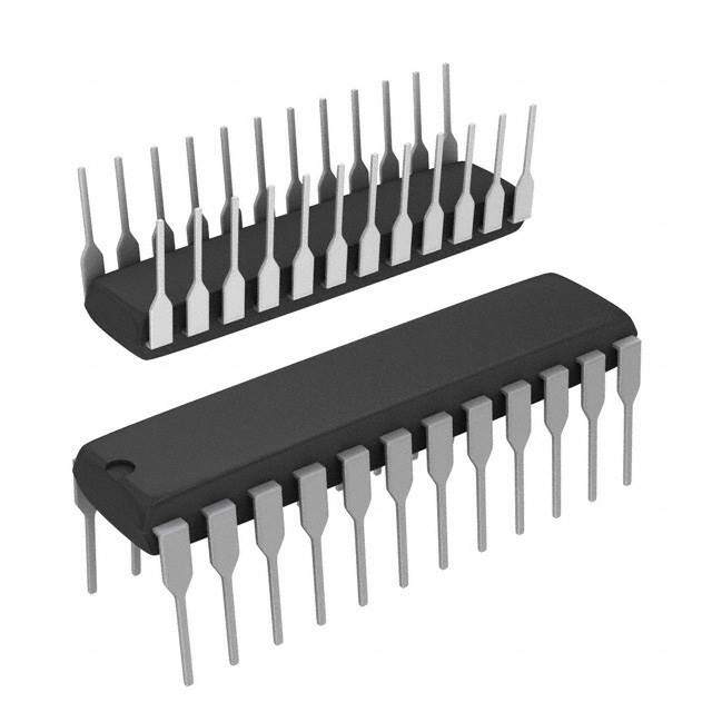
| 描述 | IC TRANSCVR TRI-ST 8BIT 24DIP总线收发器 Tri-St. Octal Bus |
| 产品分类 | |
| 品牌 | Texas Instruments |
| 产品手册 | |
| 产品图片 |
|
| rohs | 符合RoHS无铅 / 符合限制有害物质指令(RoHS)规范要求 |
| 产品系列 | 逻辑集成电路,总线收发器,Texas Instruments CD74HC652EN74HC |
| 数据手册 | |
| 产品型号 | CD74HC652EN |
| 产品目录页面 | |
| 产品种类 | 总线收发器 |
| 传播延迟时间 | 220 ns |
| 低电平输出电流 | 7.8 mA |
| 供应商器件封装 | 24-PDIP |
| 元件数 | 1 |
| 其它名称 | 296-14539-5 |
| 功能 | Tri-St. Octal Bus |
| 包装 | 管件 |
| 单位重量 | 1.754 g |
| 商标 | Texas Instruments |
| 安装类型 | 通孔 |
| 安装风格 | Through Hole |
| 封装 | Tube |
| 封装/外壳 | 24-DIP(0.300",7.62mm) |
| 封装/箱体 | PDIP-24 |
| 工作温度 | -55°C ~ 125°C |
| 工厂包装数量 | 15 |
| 最大工作温度 | + 125 C |
| 最小工作温度 | - 55 C |
| 极性 | Non-Inverting |
| 标准包装 | 15 |
| 每元件位数 | 8 |
| 每芯片的通道数量 | 8 |
| 电压-电源 | 2 V ~ 6 V |
| 电流-输出高,低 | 7.8mA,7.8mA |
| 电源电压-最大 | 6 V |
| 电源电压-最小 | 2 V |
| 电路数量 | 8 |
| 系列 | CD74HC652 |
| 输入电平 | CMOS |
| 输出电平 | CMOS |
| 输出类型 | 3-State |
| 逻辑类型 | 寄存收发器,非反相 |
| 逻辑系列 | HC |
| 高电平输出电流 | - 7.8 mA |


.jpg)


PDF Datasheet 数据手册内容提取
CD74HC652, CD74HCT652 Data sheet acquired from Harris Semiconductor SCHS194A High-Speed CMOS Logic Octal-Bus Transceiver/Registers, Three-State February 1998 - Revised May 2003 Features Description • CD74HC652, CD74HCT652 . . . . . . . . . . . Non-Inverting The CD74HC652 and CD74HCT652 three-state, octal-bus transceiver/registers use silicon-gate CMOS technology to [• /ITnditelep e(nCdDen7t4 RHegCis6t5e2rs, fCorD A7 4anHdC BT B6u5s2e)s achieveoperatingspeedssimilartoLSTTLwiththelowpower /•STuhbrjeeec-tS (taHteig Ohu-tSppuetsed CMOS Logic Octal-Bus consumption of standard CMOS integrated circuits. The Transceiver/Registers, Three-State) CD74HC652 and CD74HCT652 have non-inverting outputs. • Drives 15 LSTTL Loads Thesedevicesconsistsofbustransceivercircuits,D-typeflip- /Author () /•KTeyypwicaolrPdrso p()agationDelay=12nsatVCC=5V,CL=15pF flops, and control circuitry arranged for multiplexed transmission of data directly from the data bus or from the /•CFraenaotourt ((O)ver Temperature Range) internal storage registers. Output Enables OEAB and OEBA /D-OSCtaInNdFaOrd Opduftpmuatsrk. . . . . . . . . . . . . . .10 LSTTL Loads are provided to control the transceiver functions. SAB and - Bus Driver Outputs . . . . . . . . . . . . .15 LSTTL Loads SBA control pins are provided to select whether real-time or storeddataistransferred.Thecircuitryusedforselectcontrol [• /WPaidgee OMpoerdaeti n/gU TseemOpuetrlaitnuerse Range . . .-55oC to 125oC will eliminate the typical decoding glitch that occurs in a /•DBOalCanVcIeEdW Pr oppdafgmataiorkn Delay and Transition Times multiplexerduringthetransitionbetweenstoredandreal-time data. A LOW input level selects real-time data, and a HIGH • Significant Power Reduction Compared to LSTTL selectsstoreddata.Thefollowingexamplesdemonstratesthe Logic ICs four fundamentals bus-management functions that can be performed with the octal-bus transceivers and registers. • Alternate Source is Philips Data on the A or B data bus, or both, can be stored in the • HC Types internalDflip-flopsbylow-to-hightransitionsattheappropriate - 2V to 6V Operation clockpins(CABorCBA)regardlessoftheselectofthecontrol - High Noise Immunity: NIL = 30%, NIH = 30% of VCC pins.WhenSABandSBAareinthereal-timetransfermode,it at VCC = 5V isalsopossibletostoredatawithoutusingtheD-typeflip-flops • HCT Types by simultaneously enabling OEAB and OEBA. In this configuration, each output reinforces its input. Thus, when all - 4.5V to 5.5V Operation other data sources to the two sets of bus lines are at high - Direct LSTTL Input Logic Compatibility, impedance, each set of bus lines will remain at its last state. VIL= 0.8V (Max), VIH = 2V (Min) - CMOS Input Compatibility, Il≤1µA at VOL, VOH Ordering Information TEMP. RANGE Pinout PART NUMBER (oC) PACKAGE CD74HC652EN -55 to 125 24 Ld PDIP CD74HC652 (PDIP) CD74HCT652M -55 to 125 24 Ld SOIC CD74HCT652 CD74HCT652M96 -55 to 125 24 Ld SOIC ( SOIC) TOP VIEW NOTE: When ordering, use the entire part number. The suffix 96 denotes tape and reel. CAB 1 24 VCC SAB 2 23 CBA OEAB 3 22 SBA A0 4 21 OEBA A1 5 20 B0 A2 6 19 B1 A3 7 18 B2 A4 8 17 B3 A5 9 16 B4 A6 10 15 B5 A7 11 14 B6 GND 12 13 B7 CAUTION: These devices are sensitive to electrostatic discharge. Users should follow proper IC Handling Procedures. Copyright © 2003, Texas Instruments Incorporated 1
CCDD7744HHCC665522,, CCDD7744HHCCTT665522 Functional Diagram 4 20 A0 B0 5 19 A1 B1 6 18 A2 B2 7 17 A A3 B3 B DATA DATA 8 16 PORT A4 B4 PORT 9 15 A5 B5 10 14 A6 B6 11 13 A7 B7 21 OEBA GND = PIN 12 3 VCC= PIN 24 OEAB 1 FLIP-FLOP CAB CLOCK 23 CLOCKS CBA CLOCK DATA 2 SOURCE SAB SOURCE 22 SELECTION SBA SOURCE INPUTS FUNCTION TABLE INPUTS DATA I/O OPERATION OR FUNCTION OEAB OEBA CAB CBA SAB SBA A0 THRU A7 B0 THRU B7 651 652 L H H or L H or L X X Input Input Isolation (Note 1) Isolation (Note 1) L H ↑ ↑ X X Store A and B Data Store A and B Data X H ↑ H or L X X Input Unspecified Store A, Hold B Store A, Hold B (Note 2) H H ↑ ↑ X X Input Output Store A in Both Store A in Both (Note 3) Registers Registers L X H or L ↑ X X Unspecified Input Hold A, Store B Hold A, Store B (Note 2) L L ↑ ↑ X X Output Input Store B in Both Store B in Both (Note 3) Registers Registers L L X X X L Output Input Real-TimeBDatato Real-TimeBDatato A Bus A Bus L L X H or L X H Stored B Data to A Stored B Data to A Bus Bus H H X X L X Input Output Real-TimeADatato Real-TimeADatato B Bus B Bus H H H or L X H X Stored A Data to B Stored A Data to B Bus Bus H L H or L H or L H H Output Output Stored A Data to B Stored A Data to B Bus and Bus Stored B Data to A Stored B Data to A Bus Bus NOTES: 1. To prevent excess currents in the High-Z (isolation) modes, all I/O terminals should be terminated with 10kΩ to 1MΩ resistors. 2. ThedataoutputfunctionsmaybeenabledordisabledbyvarioussignalsattheOEABorOEBAinputs.Datainputfunctionsarealways enabled; i.e., data at the bus pins will be stored on every low-to-high transition on the clock inputs. 3. Select Control = L: Clocks can occur simultaneously. Select Control = H: Clocks must be staggered in order to load both registers. 2
OEBA 21 VCC OEAB 3 SAB 2 TO CHANNELS 2 THRU 8 SBA C D FIG 22 7 4 U R H E 1. CAB C6 L 1 5 O 2 3 GIC CBA , C B 23 D L 7 O C 4 K VCC H D C IA † CK T G P 6 R D 5 AM A F/F 2 Q 4, (5, 6, 7, 8, N 9, 10, 11) VCC GND P † B N 20, (19, 18, 17, 16, 15, 14, 13) GND P P N N P P 24 VCC N N † Inverter not included in HC/HCT651 12 GND F/F ONE OF EIGHT IDENTICAL CHANNELS
CCDD7744HHCC665522,, CCDD7744HHCCTT665522 Absolute Maximum Ratings Thermal Information DC Supply Voltage, VCC Thermal Resistance (Typical) θJA (oC/W) (Voltages Referenced to Ground). . . . . . . . . . . . . . . . -0.5V to 7V EN (PDIP) Package (Note 4). . . . . . . . . . . . . . . . . . 67 DC Input Diode Current, IIK M (SOIC) Package (Note 5). . . . . . . . . . . . . . . . . . . 46 For VI < -0.5V or VI > VCC + 0.5V. . . . . . . . . . . . . . . . . . . . . .±20mA Maximum Junction Temperature (Hermetic Package or Die) . . .175oC DC Drain Current, IO Maximum Junction Temperature (Plastic Package) . . . . . . . .150oC For -0.5V < VO < VCC + 0.5V. . . . . . . . . . . . . . . . . . . . . . . . . .±35mA Maximum Storage Temperature Range . . . . . . . . . .-65oC to 150oC DC Output Diode Current, IOK Maximum Lead Temperature (Soldering 10s). . . . . . . . . . . . .300oC For VO < -0.5V or VO > VCC + 0.5V . . . . . . . . . . . . . . . . . . . .±20mA (SOIC - Lead Tips Only) DC Output Source or Sink Current per Output Pin, IO For VO > -0.5V or VO < VCC + 0.5V . . . . . . . . . . . . . . . . . . . .±25mA DC VCC or Ground Current, ICC . . . . . . . . . . . . . . . . . . . . . . . . .±50mA Operating Conditions Temperature Range, TA . . . . . . . . . . . . . . . . . . . . . .-55oC to 125oC Supply Voltage Range, VCC HC Types . . . . . . . . . . . . . . . . . . . . . . . . . . . . . . . . . . . . .2V to 6V HCT Types . . . . . . . . . . . . . . . . . . . . . . . . . . . . . . . . .4.5V to 5.5V DC Input or Output Voltage, VI, VO . . . . . . . . . . . . . . . . . 0V to VCC Input Rise and Fall Time 2V . . . . . . . . . . . . . . . . . . . . . . . . . . . . . . . . . . . . . . 1000ns (Max) 4.5V. . . . . . . . . . . . . . . . . . . . . . . . . . . . . . . . . . . . . . 500ns (Max) 6V . . . . . . . . . . . . . . . . . . . . . . . . . . . . . . . . . . . . . . . 400ns (Max) CAUTION:Stressesabovethoselistedin“AbsoluteMaximumRatings”maycausepermanentdamagetothedevice.Thisisastressonlyratingandoperation of the device at these or any other conditions above those indicated in the operational sections of this specification is not implied. NOTES: 4. The package thermal impedance is calculated in accordance with JESD 51-3. 5. The package thermal impedance is calculated in accordance with JESD 51-7. DC Electrical Specifications TEST CONDITIONS 25oC -40oC TO 85oC -55oC TO 125oC PARAMETER SYMBOL VI(V) VIS (V) VCC (V) MIN TYP MAX MIN MAX MIN MAX UNITS HC TYPES High Level Input VIH - - 2 1.5 - - 1.5 - 1.5 - V Voltage 4.5 3.15 - - 3.15 - 3.15 - V 6 4.2 - - 4.2 - 4.2 - V Low Level Input VIL - - 2 - - 0.3 - 0.3 - 0.3 V Voltage 4.5 - - 0.9 - 0.9 - 0.9 V 6 - - 1.2 - 1.2 - 1.2 V High Level Output VOH VIH or -0.02 2 1.9 - - 1.9 - 1.9 - V Voltage VIL -0.02 4.5 4.4 - - 4.4 - 4.4 - V CMOS Loads -0.02 6 5.9 - - 5.9 - 5.9 - V High Level Output - - - - - - - - - V Voltage -6 4.5 3.98 - - 3.84 - 3.7 - V TTL Loads -7.8 6 5.48 - - 5.34 - 5.2 - V Low Level Output VOL VIH or 0.02 2 - - 0.1 - 0.1 - 0.1 V Voltage VIL 0.02 4.5 - - 0.1 - 0.1 - 0.1 V CMOS Loads 0.02 6 - - 0.1 - 0.1 - 0.1 V Low Level Output - - - - - - - - - V Voltage 6 4.5 - - 0.26 - 0.33 - 0.4 V TTL Loads 7.8 6 - - 0.26 - 0.33 - 0.4 V 4
CCDD7744HHCC665522,, CCDD7744HHCCTT665522 DC Electrical Specifications (Continued) TEST CONDITIONS 25oC -40oC TO 85oC -55oC TO 125oC PARAMETER SYMBOL VI(V) VIS (V) VCC (V) MIN TYP MAX MIN MAX MIN MAX UNITS Input Leakage II VCC or - 6 - - ±0.1 - ±1 - ±1 µA Current GND Quiescent Device ICC VCC or 0 6 - - 8 - 80 - 160 µA Current GND Three- State Leakage VIL or VIH VO = - 6 - - ±0.5 - ±5.0 - ±10 µA Current VCC or GND HCT TYPES High Level Input VIH - - 4.5 to 2 - - 2 - 2 - V Voltage 5.5 Low Level Input VIL - - 4.5 to - - 0.8 - 0.8 - 0.8 V Voltage 5.5 High Level Output VOH VIH or -0.02 4.5 4.4 - - 4.4 - 4.4 - V Voltage VIL CMOS Loads High Level Output -6 4.5 3.98 - - 3.84 - 3.7 - V Voltage TTL Loads Low Level Output VOL VIH or 0.02 4.5 - - 0.1 - 0.1 - 0.1 V Voltage VIL CMOS Loads Low Level Output 6 4.5 - - 0.26 - 0.33 - 0.4 V Voltage TTL Loads Input Leakage II VCC 0 5.5 - ±0.1 - ±1 - ±1 µA Current and GND Quiescent Device ICC VCC or 0 5.5 - - 8 - 80 - 160 µA Current GND Three- State Leakage VIL or VIH VO = - 5.5 - - ±0.5 - ±5.0 - ±10 µA Current VCC or GND Additional Quiescent ∆ICC VCC - 4.5 to - 100 360 - 450 - 490 µA Device Current Per (Note 6) -2.1 5.5 Input Pin: 1 Unit Load NOTE: 6. For dual-supply systems theoretical worst case (VI = 2.4V, VCC = 5.5V) specification is 1.8mA. HCT Input Loading Table INPUT UNIT LOADS OEBA 1.3 OEAB 0.75 Clock A to B, B to A 0.6 Select A, Select B 0.45 Inputs A0-A7, B0-B7 0.3 NOTE: Unit Load is∆ICClimit specified in DC Electrical Specifica- tions table, e.g., 360µA max at 25oC. 5
CCDD7744HHCC665522,, CCDD7744HHCCTT665522 Prerequisite for Switching Specifications 25oC -40oC TO 85oC -55oC TO 125oC PARAMETER SYMBOL VCC(V) MIN TYP MAX MIN TYP MAX MIN TYP MAX UNITS HC TYPES Maximum Clock fMAX 2 6 - - 5 - - 4 - - MHz Frequency 4.5 30 - - 25 - - 20 - - MHz 6 35 - - 29 - - 23 - - MHz Setup Time tSU 2 60 - - 75 - - 90 - - ns Data to Clock 4.5 12 - - 15 - - 18 - - ns 6 10 - - 13 - - 15 - - ns Hold Time tH 2 35 - - 45 - - 55 - - ns Data to Clock 4.5 7 - - 9 - - 11 - - ns 6 6 - - 8 - - 9 - - ns Clock Pulse Width tW 2 80 - - 100 - - 120 - - ns 4.5 16 - - 20 - - 24 - - ns 6 14 - - 17 - - 20 - - ns HCT TYPES Maximum Clock fMAX 4.5 25 - - 20 - - 17 - - MHz Frequency Setup Time tSU 4.5 12 - - 15 - - 18 - - ns Data to Clock Hold Time tH 4.5 5 - - 5 - - 5 - - ns Data to Clock Clock Pulse Width tW 4.5 25 - - 31 - - 38 - - ns Switching SpecificationsInput tr, tf = 6ns 25oC -40oC TO 85oC -55oCTO125oC TEST VCC PARAMETER SYMBOL CONDITIONS (V) MIN TYP MAX MIN MAX MIN MAX UNITS HC TYPES Propagation Delay, tPLH, tPHL CL= 50pF 2 - - 220 - 275 - 300 ns Store A Data to B Bus 4.5 - - 44 - 55 - 66 ns Store B Data to A Bus 6 - - 37 - 47 - 5.6 ns CL= 15pF 5 - 18 - - - - - ns Propagation Delay, tPLH, tPHL CL= 50pF 2 - - 135 - 170 - 205 ns A Data to B Bus 4.5 - - 27 - 34 - 41 ns B Data to A Bus 6 - - 23 - 29 - 35 ns CL= 15pF 5 - 12 - - - - - ns Propagation Delay, tPLH, tPHL CL= 50pF 2 - - 170 - 215 - 255 ns Select to Data 4.5 - - 34 - 43 - 51 ns 6 - - 29 - 37 - 43 ns CL= 15pF 5 - 14 - - - - - ns 6
CCDD7744HHCC665522,, CCDD7744HHCCTT665522 Switching SpecificationsInput tr, tf = 6ns (Continued) 25oC -40oC TO 85oC -55oCTO125oC TEST VCC PARAMETER SYMBOL CONDITIONS (V) MIN TYP MAX MIN MAX MIN MAX UNITS Three-StateDisablingTimeBus tPLZ, tPHZ CL= 50pF 2 - - 175 - 220 - 265 ns to Output or Register to Output 4.5 - - 35 - 44 - 53 ns 6 - - 30 - 37 - 45 ns CL= 15pF 5 - 14 - - - - - ns Three-State Enabling Time Bus tPZL, tPZH CL= 50pF 2 - - 175 - 220 - 265 ns to Output or Register to Output 4.5 - - 35 - 44 - 53 ns 6 - - 30 - 37 - 45 ns CL= 15pF 5 - 14 - - - - - ns Output Transition Time tTLH, tTHL CL= 50pF 2 - - 60 - 75 - 90 ns 4.5 - - 12 - 15 - 18 ns 6 - - 10 - 13 - 15 ns Three-State Output CO - - - - 20 - 20 - 20 pF Capacitance Input Capacitance CI - - - - 10 - 10 - 10 pF Maximum Frequency fMAX CL= 15pF 5 - 60 - - - - - MHz Power Dissipation Capacitance CPD - 5 - 52 - - - - - pF (Notes 7, 8) HCT TYPES Propagation Delay, tPLH, tPHL CL= 50pF 4.5 - - 44 - 55 - 66 ns Store A Data to B Bus Store B Data to A Bus CL= 15pF 5 - 18 - - - - - ns Propagation Delay, tPLH, tPHL CL= 50pF 4.5 - - 37 - 46 - 56 ns A Data to B Bus B Data to A Bus CL= 15pF 5 - 15 - - - - - ns Propagation Delay, tPLH, tPHL CL= 50pF 4.5 - - 46 - 58 - 69 ns Select to Data CL= 15pF 5 - 19 - - - - - ns Three-StateDisablingTimeBus tPLZ, tPHZ CL= 50pF 4.5 - - 35 - 44 - 53 ns to Output or Register to Output CL= 15pF 5 - 14 - - - - - ns Three-State Enabling Time Bus tPZL, tPZH CL= 50pF 4.5 - - 45 - 56 - 68 ns to Output or Register to Output CL= 15pF 5 - 19 - - - - - ns Output Transition Time tTLH, tTHL CL= 50pF 4.5 - - 12 - 15 - 18 ns Three-State Output CO - - - - 20 - 20 - 20 pF Capacitance Input Capacitance CI - - - - 10 - 10 - 10 pF Maximum Frequency fMAX CL= 15pF 5 - 45 - - - - - MHz Power Dissipation Capacitance CPD - 5 - 52 - - - - - pF (Notes 7, 8) NOTES: 7. CPD is used to determine the dynamic power consumption, per package. 8. PD = VCC2 CPD fi +Σ VCC2 CL fowhere fi = input frequency, fo = output frequency, CL = output load capacitance, CS = switch capaci- tance, VCC = supply voltage. 7
CCDD7744HHCC665522,, CCDD7744HHCCTT665522 Test Circuits and Waveforms I trCL tfCL tWL+ tWH=fCIL trCL= 6ns tfCL= 6ns tWL+ tWH=fCL VCC 3V 90% 2.7V CLOCK 50% 50% 50% CLOCK 1.3V 1.3V 1.3V 10% 10% GND 0.3V 0.3V GND tWL tWH tWL tWH NOTE: Outputs should be switching from 10% VCC to 90% VCC in NOTE: Outputs should be switching from 10% VCC to 90% VCC in accordancewithdevicetruthtable.ForfMAX,inputdutycycle=50%. accordancewithdevicetruthtable.ForfMAX,inputdutycycle=50%. FIGURE 2. HC CLOCK PULSE RISE AND FALL TIMES AND FIGURE 3. HCT CLOCK PULSE RISE AND FALL TIMES AND PULSE WIDTH PULSE WIDTH tr = 6ns tf = 6ns tr = 6ns tf = 6ns 90% VCC 2.7V 3V INPUT 50% INPUT 1.3V 10% GND 0.3V GND tTHL tTLH tTHL tTLH 90% 90% 50% 1.3V INVERTING INVERTING 10% 10% OUTPUT OUTPUT tPHL tPLH tPHL tPLH FIGURE4. HCTRANSITIONTIMESANDPROPAGATION FIGURE 5. HCT TRANSITION TIMES AND PROPAGATION DELAY TIMES, COMBINATION LOGIC DELAY TIMES, COMBINATION LOGIC 8
CD74HC652, CD74HCT652 Test Circuits and Waveforms (Continued) trCL tfCL trCL tfCL 90% VCC CLOCK 2.7V 3V CLOCK 50% 1.3V INPUT 10% INPUT 0.3V GND GND tH(H) tH(L) tH(H) tH(L) VCC DATA 3V INDPAUTAT 50% INPUT 1.3V 1.3V 1.3V GND GND tSU(H) tSU(L) tSU(H) tSU(L) tTLH tTHL tTLH tTHL 90% 90% 90% 90% 50% OUTPUT OUTPUT 1.3V 1.3V 10% 10% tPLH tPHL tPLH tPHL tREM tREM VCC 3V SET, RESET 50% SET, RESET 1.3V OR PRESET GND OR PRESET GND IC IC CL CL 50pF 50pF FIGURE6. HCSETUPTIMES,HOLDTIMES,REMOVALTIME, FIGURE7. HCTSETUPTIMES,HOLDTIMES,REMOVALTIME, AND PROPAGATION DELAY TIMES FOR EDGE AND PROPAGATION DELAY TIMES FOR EDGE TRIGGERED SEQUENTIAL LOGIC CIRCUITS TRIGGERED SEQUENTIAL LOGIC CIRCUITS 6ns 6ns tr 6ns tf 6ns OUTPUT 90% VCC OUTPUT 2.7 3V DISABLE 50% DISABLE 1.3 10% 0.3 GND GND tPLZ tPZL tPLZ tPZL OUTPUT LOW OUTPUT LOW TO OFF 50% TO OFF 1.3V 10% 10% tPHZ 90% tPZH tPHZ 90% tPZH OUTPUT HIGH OUTPUT HIGH 50% TO OFF TO OFF 1.3V OUTPUTS OUTPUTS OUTPUTS OUTPUTS OUTPUTS OUTPUTS ENABLED DISABLED ENABLED ENABLED DISABLED ENABLED FIGURE8. HCTHREE-STATEPROPAGATIONDELAY FIGURE9. HCTTHREE-STATEPROPAGATIONDELAY WAVEFORM WAVEFORM OTHER OUTPUT INPUTS IC WITH RL = 1kΩ TIED HIGH THREE- VCC FOR tPLZ AND tPZL OR LOW STATE CL GND FOR tPHZ AND tPZH OUTPUT 50pF OUTPUT DISABLE NOTE: OpendrainwaveformstPLZandtPZLarethesameasthoseforthree-stateshownontheleft.ThetestcircuitisOutputRL=1kΩto VCC, CL = 50pF. FIGURE 10. HC AND HCT THREE-STATE PROPAGATION DELAY TEST CIRCUIT 9
PACKAGE OPTION ADDENDUM www.ti.com 15-Oct-2015 PACKAGING INFORMATION Orderable Device Status Package Type Package Pins Package Eco Plan Lead/Ball Finish MSL Peak Temp Op Temp (°C) Device Marking Samples (1) Drawing Qty (2) (6) (3) (4/5) CD74HCT652M ACTIVE SOIC DW 24 25 Green (RoHS CU NIPDAU Level-1-260C-UNLIM -55 to 125 HCT652M & no Sb/Br) CD74HCT652M96 OBSOLETE SOIC DW 24 TBD Call TI Call TI -55 to 125 CD74HCT652M96E4 OBSOLETE SOIC DW 24 TBD Call TI Call TI -55 to 125 CD74HCT652M96G4 OBSOLETE SOIC DW 24 TBD Call TI Call TI -55 to 125 (1) The marketing status values are defined as follows: ACTIVE: Product device recommended for new designs. LIFEBUY: TI has announced that the device will be discontinued, and a lifetime-buy period is in effect. NRND: Not recommended for new designs. Device is in production to support existing customers, but TI does not recommend using this part in a new design. PREVIEW: Device has been announced but is not in production. Samples may or may not be available. OBSOLETE: TI has discontinued the production of the device. (2) Eco Plan - The planned eco-friendly classification: Pb-Free (RoHS), Pb-Free (RoHS Exempt), or Green (RoHS & no Sb/Br) - please check http://www.ti.com/productcontent for the latest availability information and additional product content details. TBD: The Pb-Free/Green conversion plan has not been defined. Pb-Free (RoHS): TI's terms "Lead-Free" or "Pb-Free" mean semiconductor products that are compatible with the current RoHS requirements for all 6 substances, including the requirement that lead not exceed 0.1% by weight in homogeneous materials. Where designed to be soldered at high temperatures, TI Pb-Free products are suitable for use in specified lead-free processes. Pb-Free (RoHS Exempt): This component has a RoHS exemption for either 1) lead-based flip-chip solder bumps used between the die and package, or 2) lead-based die adhesive used between the die and leadframe. The component is otherwise considered Pb-Free (RoHS compatible) as defined above. Green (RoHS & no Sb/Br): TI defines "Green" to mean Pb-Free (RoHS compatible), and free of Bromine (Br) and Antimony (Sb) based flame retardants (Br or Sb do not exceed 0.1% by weight in homogeneous material) (3) MSL, Peak Temp. - The Moisture Sensitivity Level rating according to the JEDEC industry standard classifications, and peak solder temperature. (4) There may be additional marking, which relates to the logo, the lot trace code information, or the environmental category on the device. (5) Multiple Device Markings will be inside parentheses. Only one Device Marking contained in parentheses and separated by a "~" will appear on a device. If a line is indented then it is a continuation of the previous line and the two combined represent the entire Device Marking for that device. (6) Lead/Ball Finish - Orderable Devices may have multiple material finish options. Finish options are separated by a vertical ruled line. Lead/Ball Finish values may wrap to two lines if the finish value exceeds the maximum column width. Important Information and Disclaimer:The information provided on this page represents TI's knowledge and belief as of the date that it is provided. TI bases its knowledge and belief on information provided by third parties, and makes no representation or warranty as to the accuracy of such information. Efforts are underway to better integrate information from third parties. TI has taken and Addendum-Page 1
PACKAGE OPTION ADDENDUM www.ti.com 15-Oct-2015 continues to take reasonable steps to provide representative and accurate information but may not have conducted destructive testing or chemical analysis on incoming materials and chemicals. TI and TI suppliers consider certain information to be proprietary, and thus CAS numbers and other limited information may not be available for release. In no event shall TI's liability arising out of such information exceed the total purchase price of the TI part(s) at issue in this document sold by TI to Customer on an annual basis. Addendum-Page 2
None
IMPORTANTNOTICE TexasInstrumentsIncorporatedanditssubsidiaries(TI)reservetherighttomakecorrections,enhancements,improvementsandother changestoitssemiconductorproductsandservicesperJESD46,latestissue,andtodiscontinueanyproductorserviceperJESD48,latest issue.Buyersshouldobtainthelatestrelevantinformationbeforeplacingordersandshouldverifythatsuchinformationiscurrentand complete.Allsemiconductorproducts(alsoreferredtohereinas“components”)aresoldsubjecttoTI’stermsandconditionsofsale suppliedatthetimeoforderacknowledgment. TIwarrantsperformanceofitscomponentstothespecificationsapplicableatthetimeofsale,inaccordancewiththewarrantyinTI’sterms andconditionsofsaleofsemiconductorproducts.TestingandotherqualitycontroltechniquesareusedtotheextentTIdeemsnecessary tosupportthiswarranty.Exceptwheremandatedbyapplicablelaw,testingofallparametersofeachcomponentisnotnecessarily performed. TIassumesnoliabilityforapplicationsassistanceorthedesignofBuyers’products.Buyersareresponsiblefortheirproductsand applicationsusingTIcomponents.TominimizetherisksassociatedwithBuyers’productsandapplications,Buyersshouldprovide adequatedesignandoperatingsafeguards. TIdoesnotwarrantorrepresentthatanylicense,eitherexpressorimplied,isgrantedunderanypatentright,copyright,maskworkright,or otherintellectualpropertyrightrelatingtoanycombination,machine,orprocessinwhichTIcomponentsorservicesareused.Information publishedbyTIregardingthird-partyproductsorservicesdoesnotconstitutealicensetousesuchproductsorservicesorawarrantyor endorsementthereof.Useofsuchinformationmayrequirealicensefromathirdpartyunderthepatentsorotherintellectualpropertyofthe thirdparty,oralicensefromTIunderthepatentsorotherintellectualpropertyofTI. ReproductionofsignificantportionsofTIinformationinTIdatabooksordatasheetsispermissibleonlyifreproductioniswithoutalteration andisaccompaniedbyallassociatedwarranties,conditions,limitations,andnotices.TIisnotresponsibleorliableforsuchaltered documentation.Informationofthirdpartiesmaybesubjecttoadditionalrestrictions. ResaleofTIcomponentsorserviceswithstatementsdifferentfromorbeyondtheparametersstatedbyTIforthatcomponentorservice voidsallexpressandanyimpliedwarrantiesfortheassociatedTIcomponentorserviceandisanunfairanddeceptivebusinesspractice. TIisnotresponsibleorliableforanysuchstatements. Buyeracknowledgesandagreesthatitissolelyresponsibleforcompliancewithalllegal,regulatoryandsafety-relatedrequirements concerningitsproducts,andanyuseofTIcomponentsinitsapplications,notwithstandinganyapplications-relatedinformationorsupport thatmaybeprovidedbyTI.Buyerrepresentsandagreesthatithasallthenecessaryexpertisetocreateandimplementsafeguardswhich anticipatedangerousconsequencesoffailures,monitorfailuresandtheirconsequences,lessenthelikelihoodoffailuresthatmightcause harmandtakeappropriateremedialactions.BuyerwillfullyindemnifyTIanditsrepresentativesagainstanydamagesarisingoutoftheuse ofanyTIcomponentsinsafety-criticalapplications. Insomecases,TIcomponentsmaybepromotedspecificallytofacilitatesafety-relatedapplications.Withsuchcomponents,TI’sgoalisto helpenablecustomerstodesignandcreatetheirownend-productsolutionsthatmeetapplicablefunctionalsafetystandardsand requirements.Nonetheless,suchcomponentsaresubjecttotheseterms. NoTIcomponentsareauthorizedforuseinFDAClassIII(orsimilarlife-criticalmedicalequipment)unlessauthorizedofficersoftheparties haveexecutedaspecialagreementspecificallygoverningsuchuse. OnlythoseTIcomponentswhichTIhasspecificallydesignatedasmilitarygradeor“enhancedplastic”aredesignedandintendedforusein military/aerospaceapplicationsorenvironments.BuyeracknowledgesandagreesthatanymilitaryoraerospaceuseofTIcomponents whichhavenotbeensodesignatedissolelyattheBuyer'srisk,andthatBuyerissolelyresponsibleforcompliancewithalllegaland regulatoryrequirementsinconnectionwithsuchuse. TIhasspecificallydesignatedcertaincomponentsasmeetingISO/TS16949requirements,mainlyforautomotiveuse.Inanycaseofuseof non-designatedproducts,TIwillnotberesponsibleforanyfailuretomeetISO/TS16949. Products Applications Audio www.ti.com/audio AutomotiveandTransportation www.ti.com/automotive Amplifiers amplifier.ti.com CommunicationsandTelecom www.ti.com/communications DataConverters dataconverter.ti.com ComputersandPeripherals www.ti.com/computers DLP®Products www.dlp.com ConsumerElectronics www.ti.com/consumer-apps DSP dsp.ti.com EnergyandLighting www.ti.com/energy ClocksandTimers www.ti.com/clocks Industrial www.ti.com/industrial Interface interface.ti.com Medical www.ti.com/medical Logic logic.ti.com Security www.ti.com/security PowerMgmt power.ti.com Space,AvionicsandDefense www.ti.com/space-avionics-defense Microcontrollers microcontroller.ti.com VideoandImaging www.ti.com/video RFID www.ti-rfid.com OMAPApplicationsProcessors www.ti.com/omap TIE2ECommunity e2e.ti.com WirelessConnectivity www.ti.com/wirelessconnectivity MailingAddress:TexasInstruments,PostOfficeBox655303,Dallas,Texas75265 Copyright©2015,TexasInstrumentsIncorporated