ICGOO在线商城 > 射频/IF 和 RFID > RF 评估和开发套件,板 > CC2400DBK

 Datasheet下载
- 型号: CC2400DBK
- 制造商: Texas Instruments
- 库位|库存: xxxx|xxxx
- 要求:
| 数量阶梯 | 香港交货 | 国内含税 |
| +xxxx | $xxxx | ¥xxxx |
查看当月历史价格
查看今年历史价格
CC2400DBK产品简介:
ICGOO电子元器件商城为您提供CC2400DBK由Texas Instruments设计生产,在icgoo商城现货销售,并且可以通过原厂、代理商等渠道进行代购。 CC2400DBK价格参考。Texas InstrumentsCC2400DBK封装/规格:RF 评估和开发套件,板, 。您可以下载CC2400DBK参考资料、Datasheet数据手册功能说明书,资料中有CC2400DBK 详细功能的应用电路图电压和使用方法及教程。
Texas Instruments(TI)的CC2400DBK是一款基于CC2400芯片的射频(RF)评估与开发套件,主要用于无线通信系统的开发与测试。该套件支持2.4 GHz全球通用ISM频段,适用于多种低功耗无线应用。

CC2400DBK广泛应用于以下场景:

1. 无线传感器网络:用于构建低功耗、低成本的传感节点,如温湿度监测、工业控制和环境监控系统。
2. 智能家居设备开发:可用于开发ZigBee兼容的智能照明、安防系统、家电控制等产品。
3. 无线遥控与遥测:适用于玩具、无人机或机器人远程控制等场景,提供可靠的无线数据传输。
4. 无线音频传输:在低延迟、低功耗的音频流应用中,如无线耳机、麦克风等。
5. 医疗健康设备:如便携式心率监测仪、运动追踪设备等需低功耗无线连接的场合。
6. 无线更新与调试平台:作为硬件平台,帮助工程师进行射频性能测试、协议优化及固件升级。

总之,CC2400DBK是为开发者提供快速原型设计与性能验证的理想工具,尤其适合需要在2.4 GHz频段实现高效无线通信的应用场景。
| 参数 | 数值 |
| 产品目录 | |
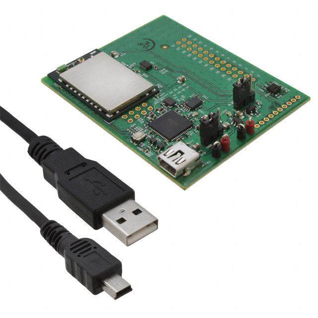
| 描述 | KIT DEMO BOARD FOR CC2400Zigbee/802.15.4开发工具 CC2400 2.4GHz DEMONSTRATION KIT |
| 产品分类 | |
| 品牌 | Texas Instruments |
| 产品手册 | |
| 产品图片 | |
| rohs | 否含铅 / 不符合限制有害物质指令(RoHS)规范要求 |
| 产品系列 | 射频/无线开发工具,Zigbee/802.15.4开发工具,Texas Instruments CC2400DBKSmartRF® |
| mouser_ship_limit | 此产品可能需要其他文件才能从美国出口。 |
| 数据手册 | |
| 产品型号 | CC2400DBK |
| 产品 | Demonstration Kits |
| 产品种类 | Zigbee/802.15.4开发工具 |
| 制造商产品页 | http://www.ti.com/general/docs/suppproductinfo.tsp?distId=10&orderablePartNumber=CC2400DBK |
| 商标 | Texas Instruments |
| 天线连接器类型 | SMA |
| 工作电源电压 | 4 V to 10 V |
| 工具用于评估 | CC2400 |
| 工厂包装数量 | 1 |
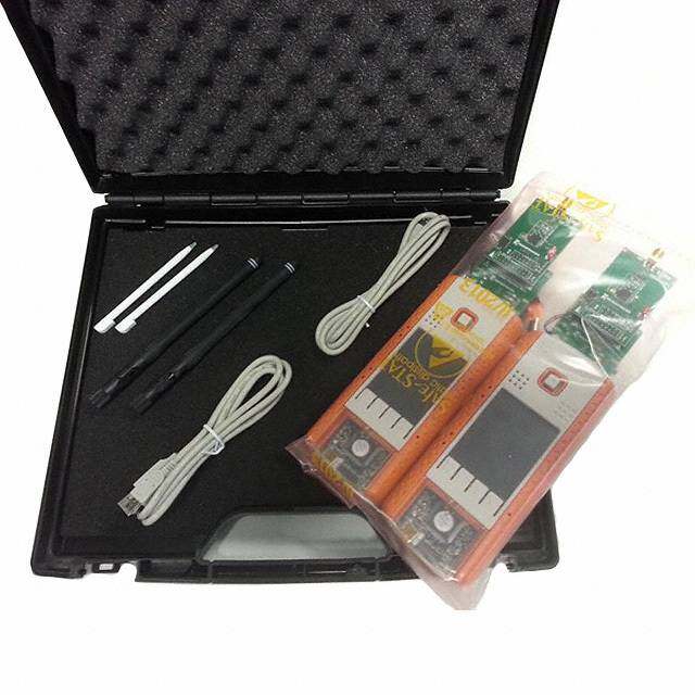
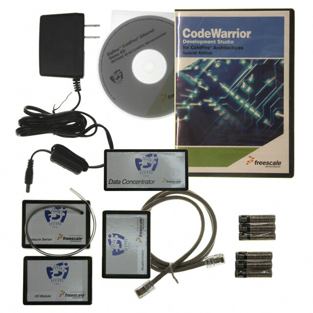
| 所含物品 | 2 个板,线缆,产品样品 |
| 接口类型 | RS-232 |
| 描述/功能 | Includes two CC2400DB Demonstration Boards |
| 标准包装 | 1 |
| 用于 | SmartRF04EB |
| 相关产品 | /product-detail/zh/CC2400-RTR1/CC2400-RTR1-ND/1690527/product-detail/zh/CC2400-RTB1/CC2400-RTB1-ND/1690526/product-detail/zh/CC2400RSU/296-32847-5-ND/1690525/product-detail/zh/CC2400RSUR/296-21512-1-ND/1304552/product-detail/zh/CC2400RTC/296-19466-ND/998339 |
| 类型 | 收发器,ISM |
| 配套使用产品/相关产品 | CC2400 |
| 频率 | 2.4 GHz |


- 商务部:美国ITC正式对集成电路等产品启动337调查
- 曝三星4nm工艺存在良率问题 高通将骁龙8 Gen1或转产台积电
- 太阳诱电将投资9.5亿元在常州建新厂生产MLCC 预计2023年完工
- 英特尔发布欧洲新工厂建设计划 深化IDM 2.0 战略
- 台积电先进制程称霸业界 有大客户加持明年业绩稳了
- 达到5530亿美元!SIA预计今年全球半导体销售额将创下新高
- 英特尔拟将自动驾驶子公司Mobileye上市 估值或超500亿美元
- 三星加码芯片和SET,合并消费电子和移动部门,撤换高东真等 CEO
- 三星电子宣布重大人事变动 还合并消费电子和移动部门
- 海关总署:前11个月进口集成电路产品价值2.52万亿元 增长14.8%

PDF Datasheet 数据手册内容提取
CC2400 CC2400 2.4 GHz Low-Power RF Transceiver Applications • 2.4 GHz MHz ISM/SRD band systems • Wireless audio • Game controllers • PC peripherals • Sports and leisure equipment • Advanced toys Product Description The CC2400 is a true single-chip 2.4 GHz and error detection reducing the workload RF transceiver designed for low-power on the host microcontroller. and low-voltage wireless applications. The RF transceiver is integrated with a The main operating parameters of CC2400 baseband modem supporting data rates can be programmed via an SPI-bus. In a up to 1 Mbps. typical system CC2400 will be used together with a microcontroller and a few The CC2400 is a low-cost, highly integrated external, passive components. solution enabling robust wireless communication in the 2.4 - 2.4835 GHz CC2400 is based on Chipcon’s SmartRF®- unlicensed ISM band. It is intended for 03 technology in 0.18 µm CMOS. systems compliant with world-wide regulations covered by EN 300 440 (Europe), CFR47 Part 15 (US) and ARIB STD-T66 (Japan). Targeting a wide range of applications at 2.4 GHz, the CC2400 supports over-the-air data rates of 10 kbps, 250 kbps and 1 Mbps without requiring any modifications to the hardware. The CC2400 provides extensive hardware support for packet handling, data buffering, burst transmissions, data coding Key Features • True single-chip 2.4 GHz RF • Packet handling hardware transceiver with baseband modem • Data buffering • 10 kbps, 250 kbps and 1 Mbps over- • Digital RSSI output the-air data rates • Small size (QFN 48 package), 7x7 mm • Low current consumption (RX: 24 mA) • Reference design complies with EN • Low core supply voltage (1.8 V) 300 328, EN 300 440, FCC CFR47 part • Programmable output power 15 and ARIB STD-T66 • No external RF switch / filter needed • Powerful and flexible development • I/Q low-IF receiver tools available • I/Q direct up-conversion transmitter • Easy-to-use software for generating the • Few external components CC2400 configuration data • FIFO allows bursting of data This document contains information on a pre-production product. Specifications and information herein are subject to change without notice. SWRS042A Page 1 of 83
CC2400 Table of contents 1 ABBREVIATIONS..............................................................................................................4 2 FEATURES........................................................................................................................5 3 ABSOLUTE MAXIMUM RATINGS....................................................................................6 4 OPERATING CONDITIONS..............................................................................................6 5 ELECTRICAL SPECIFICATIONS.....................................................................................7 6 GENERAL CHARACTERISTICS......................................................................................7 7 RF TRANSMIT SECTION..................................................................................................8 8 RF RECEIVE SECTION.....................................................................................................9 9 AFC SECTION.................................................................................................................10 10 RSSI / CARRIER SENSE SECTION............................................................................11 11 IF SECTION..................................................................................................................11 12 FREQUENCY SYNTHESIZER SECTION....................................................................11 13 DIGITAL INPUTS/OUTPUTS.......................................................................................12 14 PIN ASSIGNMENT.......................................................................................................13 15 CIRCUIT DESCRIPTION.............................................................................................15 16 APPLICATION CIRCUIT..............................................................................................17 16.1 INPUT / OUTPUT MATCHING.......................................................................................17 16.2 BIAS RESISTOR........................................................................................................17 16.3 CRYSTAL.................................................................................................................17 16.4 DIGITAL I/O.............................................................................................................17 16.5 POWER SUPPLY DECOUPLING AND FILTERING............................................................17 16.6 POWER SUPPLY SWITCHING......................................................................................17 17 CONFIGURATION OVERVIEW...................................................................................20 18 CONFIGURATION SOFTWARE..................................................................................20 19 4-WIRE SERIAL CONFIGURATION INTERFACE......................................................21 20 OVERVIEW OF CONFIGURATIONS AND HARDWARE SUPPORT........................24 21 MICROCONTROLLER INTERFACE AND PIN CONFIGURATION...........................25 21.1 CONFIGURATION INTERFACE.....................................................................................25 21.2 SIGNAL INTERFACE IN UN-BUFFERED MODE................................................................25 21.3 GENERAL CONTROL AND STATUS PINS.......................................................................25 22 DATA BUFFERING......................................................................................................27 22.1 BUFFERED MODE.....................................................................................................27 22.2 BUFFERED MODE HARDWARE SUPPORT.....................................................................27 23 PACKET HANDLING HARDWARE SUPPORT..........................................................29 23.1 DATA PACKET FORMAT.............................................................................................29 23.2 ERROR DETECTION..................................................................................................29 23.3 HARDWARE INTERFACE............................................................................................31 24 DATA / LINE ENCODING............................................................................................31 24.1 DATA ENCODING IN BUFFERED MODE.........................................................................31 24.2 DATA ENCODING IN UN-BUFFERED MODE...................................................................32 25 RADIO CONTROL STATE MACHINE........................................................................34 26 POWER MANAGEMENT FLOW CHART...................................................................36 27 FSK MODULATION FORMATS..................................................................................38 28 BUILT-IN TEST PATTERN GENERATOR..................................................................38 29 RECEIVER CHANNEL BANDWIDTH.........................................................................39 30 DATA RATE PROGRAMMING....................................................................................40 31 DEMODULATOR, BIT SYNCHRONIZER AND DATA DECISION.............................41 32 AUTOMATIC FREQUENCY CONTROL.....................................................................42 33 LINEAR IF AND AGC SETTINGS...............................................................................43 34 RSSI..............................................................................................................................44 35 CARRIER SENSE........................................................................................................45 36 INTERFACING AN EXTERNAL LNA OR PA.............................................................45 37 GENERAL PURPOSE / TEST OUTPUT CONTROL PINS.........................................45 38 FREQUENCY PROGRAMMING..................................................................................47 38.1 TRANSMIT MODE......................................................................................................47 SWRS042A Page 2 of 83
CC2400 38.2 RECEIVE MODE........................................................................................................47 39 ALTERNATE TX IF SETTING.....................................................................................47 40 VCO..............................................................................................................................48 41 VCO SELF-CALIBRATION..........................................................................................48 42 OUTPUT POWER PROGRAMMING...........................................................................48 43 CRYSTAL OSCILLATOR............................................................................................49 44 INPUT / OUTPUT MATCHING.....................................................................................50 45 TYPICAL PERFORMANCE GRAPHS.........................................................................50 46 SYSTEM CONSIDERATIONS AND GUIDELINES.....................................................53 46.1 SRD REGULATIONS..................................................................................................53 46.2 FREQUENCY HOPPING AND MULTI-CHANNEL SYSTEMS................................................53 46.3 DATA BURST TRANSMISSIONS...................................................................................53 46.4 CONTINUOUS TRANSMISSIONS..................................................................................53 46.5 CRYSTAL DRIFT COMPENSATION...............................................................................53 46.6 SPECTRUM EFFICIENT MODULATION..........................................................................54 46.7 LOW LATENCY SYSTEMS...........................................................................................54 46.8 LOW COST SYSTEMS................................................................................................54 46.9 BATTERY OPERATED SYSTEMS..................................................................................54 46.10 INCREASING OUTPUT POWER....................................................................................54 47 PCB LAYOUT RECOMMENDATIONS.......................................................................56 48 ANTENNA CONSIDERATIONS..................................................................................57 49 CONFIGURATION REGISTERS.................................................................................58 50 PACKAGE DESCRIPTION (QFN48)...........................................................................76 51 RECOMMENDED LAYOUT FOR PACKAGE (/QFN48).............................................77 52 PACKAGE THERMAL PROPERTIES.........................................................................77 53 SOLDERING INFORMATION......................................................................................77 54 IC MARKING................................................................................................................78 55 PLASTIC TUBE SPECIFICATION...............................................................................80 56 CARRIER TAPE AND REEL SPECIFICATION..........................................................80 57 ORDERING INFORMATION........................................................................................80 58 GENERAL INFORMATION..........................................................................................81 58.1 DOCUMENT HISTORY...............................................................................................81 58.2 PRODUCT STATUS DEFINITIONS................................................................................82 58.3 DISCLAIMER.............................................................................................................82 58.4 TRADEMARKS..........................................................................................................82 58.5 LIFE SUPPORT POLICY.............................................................................................82 59 ADDRESS INFORMATION..........................................................................................83 SWRS042A Page 3 of 83
CC2400 1 Abbreviations ACP Adjacent Channel Power ACR Adjacent Channel Rejection ADC Analog-to-Digital Converter AFC Automatic Frequency Correction AGC Automatic Gain Control BER Bit Error Rate BOM Bill Of Materials bps bits per second BT Bandwidth-Time product (for GFSK) CRC Cyclic Redundancy Check CSMA Carrier Sense Multiple Access CSMA / CA Carrier Sense Multiple Access / Collision Avoidance DAC Digital-to-Analog Converter ESR Equivalent Series Resistance FH Frequency Hopping FHSS Frequency Hopping Spread Spectrum FIFO First In First Out (queue) FS Frequency Synthesizer FSK Frequency Shift Keying GFSK Gaussian Frequency Shift Keying IF Intermediate Frequency ISM Industrial Scientific Medical kbps kilo bits per second LNA Low Noise Amplifier Mbps Mega bits per second MCU Micro Controller Unit NRZ Non Return to Zero PA Power Amplifier PD Phase Detector PCB Printed Circuit Board PN9 Pseudo-random Bit Sequence (9-bit) PLL Phase Locked Loop PRN Pseudo Random Number PRNG Pseudo Random Number Generator RF Radio Frequency RSSI Received Signal Strength Indicator RX Receive (mode) SPI Serial Peripheral Interface SRD Short Range Device TBD To Be Decided/Defined TDMA Time Division Multiple Access TX Transmit (mode) VCO Voltage Controlled Oscillator VGA Variable Gain Amplifier SWRS042A Page 4 of 83
CC2400 2 Features • 2400 – 2483 MHz RF transceiver • GFSK and FSK modulation • Packet handling hardware support • Very low current consumption (RX: • Preamble generator with 24 mA) programmable length • Over-the-air data rates of 10 kbps, • Programmable synchronization 250 kbps and 1 Mbps word insertion/detection • High sensitivity (-87 dBm @ 1Mbps, • CRC computation over the data BER=10-3) field • Agile frequency synthesizer (40 us • 8B/10B line coding option settling time) • On-chip VCO, LNA and PA • Data buffering • Low core supply voltage (1.6-2.0 V) • 32 byte FIFO • Flexible I/O supply voltage • Provides for flexible communication (1.6–3.6 V) to match the signal with the host controller. levels of the interfacing • Burst transmission reduces the microcontroller average power consumption. • Programmable output power • I/Q low-IF receiver • Powerful and flexible development • I/Q direct up-conversion transmitter tools available • Fully equipped development kit • Few external components • Demonstration board reference • Only reference crystal and a few design with microcontroller code passives needed • Easy-to-use SmartRF Studio • No external filters needed software for generating the CC2400 configuration data • Programmable baseband modem • 4-wire SPI interface • Small size (QFN 48 package) 7 x 7 mm • Serial clock up to 20 MHz • Digital RSSI output • Reference design complies with EN 300 328, EN 300 440, FCC CFR47 part 15 and ARIB STD-T66 SWRS042A Page 5 of 83
CC2400 3 Absolute Maximum Ratings Parameter Min. Max. Units Condition Supply voltage, chip core, −0.3 2.0 V AVDD/DVDD1.8=VDD Supply voltage (DVDD3.3=VDDIO), digital I/O −0.3 3.6 V Voltage on any pin, core −0.3 VDD+0.3, V max 2.0 Voltage on any pin, digital I/O (pin no. 27-35) −0.3 VDDIO+0.3, V max 3.6 Input RF level 10 dBm Storage temperature range −50 150 °C Reflow solder temperature 260 °C T = 10 s NOTE: The supply voltage to the chip core (AVDD/DVDD1.8) should not be switched off when the digital IO (DVDD3.3) supply voltage is still applied to the chip. If this is done, a large current will flow inside the CC2400 and the chip may be damaged as a result. If the core supply needs to be switched off to lower the power consumption, please see page 17 for a suggested solution. The absolute maximum ratings given the limiting values may cause permanent above should under no circumstances be damage to the device. violated. Stress exceeding one or more of Caution! ESD sensitive device. Precaution should be used when handling the device in order to prevent permanent damage. 4 Operating Conditions Parameter Min. Typ. Max. Unit Condition Supply voltage, chip core, 1.6 2.0 V AVDD/DVDD1.8 Supply voltage (DVDD3.3), digital 1.6 3.6 V The digital I/O voltage (DVDD3.3 I/O, VDDIO pin) must match the interfacing circuit. Recommended supply voltage, chip 1.8V core, AVDD/DVDD1.8 Recommended supply voltage 1.8V/ (DVDD3.3), digital I/O 3.3V Operating ambient temperature −40 85 °C range SWRS042A Page 6 of 83
CC2400 5 Electrical Specifications Parameter Min. Typ. Max. Unit Condition / Note Current Consumption, Power Down mode (OFF) 1.5 5 µA Oscillator core off Current Consumption, Idle mode (IDLE) 1.2 mA Current Consumption, Frequency synthesizer (FS_ON) 6.3 mA Current Consumption, 24 mA Receive mode Current Consumption, Transmit mode: P=−25 dBm 11 mA The output power is delivered differentially to a 50Ω single- P=−5 dBm 15 mA ended load through a balun, see also p. 50. P=0 dBm 19 mA Current Consumption, crystal 38 µA 16 MHz, 16 pF load crystal oscillator core Table 1 Electrical specifications 6 General Characteristics Tc = 25°C, AVDD/DVDD1.8 = 1.8 V, DVDD3.3 = 3.3V (digital I/O) if nothing else stated. Measured on Chipcon’s CC2400EM reference design. Parameter Min. Typ. Max. Unit Condition / Note RF Frequency Range 2400 2483 MHz Programmable in 1 MHz channel steps. Data rate 10 kbps Data rate is 250 kbps programmable/selectable, see 1 Mbps page 40 Table 2 General characteristics SWRS042A Page 7 of 83
CC2400 7 RF Transmit section Tc = 25°C, AVDD/DVDD1.8 = 1.8 V, DVDD3.3 = 3.3V (digital I/O) if nothing else stated. Measured on Chipcon’s CC2400EM reference design. Parameter Min. Typ. Max. Unit Condition / Note Binary FSK frequency deviation 0 250 500 ±kHz The frequency corresponding to the digital "0" is denoted f, while 0 f corresponds to a digital "1". 1 The frequency deviation is given by f=±(f−f)/2. The RF carrier d 1 0 frequency, f, is then given by c f=(f+f)/2. c 0 1 Nominal output power 0 dBm Default settings. Power delivered to a 50 Ω single- ended load through a balun. The output power is programmable in 8 steps. Programmable output power range 25 dB 20 dB bandwidth Maximum output power. Modulation is 1 Mbps, NRZ data, FSK 1.2 MHz ± 250 kHz frequency deviation. GFSK 1.0 MHz Adjacent Channel Power (ACP) Maximum output power. Modulation is 1 Mbps, NRZ data, FSK -30 dBc ± 250 kHz frequency deviation. GFSK -43 dBc Measured at 2 MHz offset. Harmonics At max output power delivered to 2nd order harmonic -41 dBm 50 Ω single-ended load through a 3rd order harmonic -54 dBm balun. Carrier modulated with pseudo-random data. See p.50. Spurious emission Maximum output power. 30 - 1000 MHz -65 -36 dBm Modulation is 1 Mbps FSK, NRZ 1– 12.75 GHz -41 -30 dBm data, ±250 kHz frequency 1.8 – 1.9 GHz -69 -47 dBm deviation. 5.15 – 5.3 GHz -65 -47 dBm Complying with EN 300 440, CFR47 Part 15 and ARIB STD- T66 Optimum load impedance 110 Ω Differential impedance as seen + j130 from the RF-port (RF_P and RF_N) towards the antenna. For matching details see “Input/ output matching” page 50 as well as the application circuit description on page 17. Table 3 Transmit characteristics SWRS042A Page 8 of 83
CC2400 8 RF Receive section Tc = 25°C, AVDD/DVDD1.8 = 1.8 V, DVDD3.3 = 3.3V (digital I/O) if nothing else stated. Measured on Chipcon’s CC2400EM reference design. Parameter Min. Typ. Max. Unit Condition / Note Receiver Sensitivity at BER = 10−3 Measured in a 50 Ohm single- ended load through a balun. FSK, NRZ mode used. 1 Mbps, 1 MHz channel BW -87 dBm ±250 kHz frequency deviation 250 kbps, 1 MHz channel BW -91 dBm ±250 kHz frequency deviation 10 kbps, 500 kHz channel BW -101 dBm ±125 kHz frequency deviation Saturation (maximum input level) 3 dBm Maximum gain in LNA. NRZ coded data, BER = 10−3 Co-channel rejection -10 dB 1 Mbps wanted signal 10 dB above the sensitivity level, interferer modulated like signal (pseudo-random FSK, ± 250 kHz deviation), interferer at operating frequency, BER = 10−3 Adjacent channel rejection (ACR) FSK wanted signal 10 dB above the sensitivity level, 1 MHz 1 Mbps 0 dB channel spacing, interferer 250 kbps 12 dB modulated like signal (pseudo- random FSK, ± 250 kHz deviation) at adjacent channel, BER = 10−3 Image channel rejection FSK wanted signal 10 dB above the sensitivity level, interferer 1 Mbps 21 dB modulated like signal (pseudo- 250 kbps 39 dB random FSK, ± 250 kHz deviation) at image frequency, BER = 10−3. The image channel is centered 2MHz below the center frequency of the desired channel. Selectivity (C/I) (In-band channel rejection) + 2MHz 20 dB 1Mbps FSK wanted signal at ± 3MHz 41 dB 2441 MHz, 3 dB above the ± 4MHz 50 dB sensitivity level (except + 2 MHz, ± 5MHz 52 dB which is 10 dB above the ± 10MHz 55 dB sensitivity limit), jammer ± 20 MHz 56 dB modulated like signal (pseudo- ± 50MHz 59 dB random, ± 250 kHz deviation) at ± 2-39 MHz in 1 MHz steps offset, BER = 10−3. Adjacent channels and image channel are excluded. + 2 MHz 48 dB 250 kbps FSK wanted signal at ± 3 MHz 50 dB 2441 MHz, 3 dB above the ± 4 MHz 55 dB sensitivity level (except + 2 MHz, ± 5 MHz 56 dB which is 10 dB above the ± 10 MHz 59 dB sensitivity limit), jammer ± 20 MHz 60 dB modulated like signal (pseudo- ± 50 MHz 64 dB random, ± 250 kHz deviation) at ± 2-39 MHz in 1 MHz steps offset, BER = 10−3. Adjacent channels and image channel are excluded. SWRS042A Page 9 of 83
CC2400 Parameter Min. Typ. Max. Unit Condition / Note Blocking / Desensitization* (*out-of-band spurious response rejection) 0.3 – 2.0 GHz 71 dB 1 Mbps FSK wanted signal 3 dB 2.0 – 2.399 GHz 50 dB above the sensitivity level, sine- 2.498 – 3.0 GHz 49 dB wave interfering signal, BER = 3 – 12.75 GHz 76 dB 10−3. Input IIP3 Measured directly by applying two Out of band -5 dBm tones and measuring the In band -17 dBm resulting difference tone amplitude. Image frequency suppression 56 dB Ratio between sensitivity for a signal at the image frequency and the sensitivity in the wanted channel with an inverted signal. The image frequency is centered -2 MHz from the center of the wanted channel. The signal source is 1Mbps, NRZ coded data, ±250 kHz frequency deviation, signal level for BER = 10−3 Spurious reception 80 dB Ratio between the sensitivity for an unwanted frequency and the sensitivity in the wanted channel. The signal source is a 1 Mbps, NRZ coded data, ±250 kHz frequency deviation, swept over all frequencies 2400 – 2483.5 MHz. Signal level for BER = 10−3 Adjacent channels and image channel are excluded. Spurious emission Complying with EN 300 440, < 1 GHz −70 -57 dBm CFR47 Part 15 and ARIB STD- 1 – 12.75 GHz −56 -47 dBm T66 Table 4 RF Receive characteristics 9 AFC section Parameter Min. Typ. Max. Unit Condition / Note For 1Mbps and 1 MHz channel width, AFC_SETTLING=4. AFC range ± 500 kHz Measured using an unmodulated carrier. AFC accuracy 5 kHz Table 5 AFC characteristics SWRS042A Page 10 of 83
CC2400 10 RSSI / Carrier Sense section Parameter Min. Typ. Max. Unit Condition / Note For 1Mbps and 1 MHz channel width. RSSI range / Carrier sense range 80 dB (The range is from –100 dBm to –20 dBm typically) RSSI settling time 20 µs RSSI accuracy ± 4 dB See page 44 for details Table 6 RSSI / Carrier sense characteristics 11 IF section Parameter Min. Typ. Max. Unit Condition / Note Intermediate frequency (IF) 1 MHz Digital channel filter bandwidth 125 1000 kHz The digital channel filter 6dB- bandwidth is programmable in steps: 125, 250, 500 and 1000 kHz. See page 39 for details. Table 7 IF characteristics 12 Frequency Synthesizer section Parameter Min. Typ. Max. Unit Condition / Note Crystal oscillator frequency 16 MHz See page 49 for details. Crystal frequency accuracy 20 ±ppm The total crystal frequency requirement accuracy, i.e. initial tolerance plus aging and temperature dependency, will determine the frequency accuracy of the transmitted signal. 1 Mbps FSK, 250 kHz deviation. Crystal operation Parallel C4 and C5 are loading capacitors, see page 49 Crystal load capacitance 12 16 20 pF 16 pF recommended Crystal ESR 60 Ω Crystal oscillator start-up time 1.13 ms 16 pF load Note: This time can be reduced to 15 µs by enabling the XOSC core in power-down using the MANAND register. Phase noise Unmodulated carrier -108 dBc/Hz At ±1 MHz offset from carrier -114 dBc/Hz At ±2 MHz offset from carrier -114 dBc/Hz At ±5 MHz offset from carrier PLL loop bandwidth 50 kHz SWRS042A Page 11 of 83
CC2400 Parameter Min. Typ. Max. Unit Condition / Note PLL lock time (RX / TX turn-on 40 µs Until within ± 10 kHz time) Step size is 1MHz, no calibration. Note: Calibration should be performed for frequency changes > 8 MHz. PLL turn-on time from IDLE mode, 100 µs Crystal oscillator running. crystal oscillator on Calibration time included. Table 8 Frequency synthesizer characteristics 13 Digital Inputs/Outputs Parameter Min. Typ. Max. Unit Condition / Note Signal levels are referred to the voltage level at the pin DVDD3.3. Logic "0" input voltage 0 0.3* V DVDD Logic "1" input voltage 0.7* DVDD V DVDD Logic "0" output voltage 0 0.4 V Output current −8 mA, 3.3 V supply voltage Logic "1" output voltage 2.5 DVDD V Output current 8 mA, 3.3 V supply voltage Logic "0" input current NA −1 µA Input signal equals GND Logic "1" input current NA 1 µA Input signal equals DVDD DIO setup time 20 ns TX un-buffered mode, minimum time DIO must be ready before the positive edge of DCLK DIO hold time 10 ns TX un-buffered mode, minimum time DIO must be held after the positive edge of DCLK Serial interface (SCLK, SI, SO and See Table 12 page 22 CSn) timing specification Table 9 Digital input/output characteristics SWRS042A Page 12 of 83
CC2400 14 Pin Assignment 1 2 C AVDD_CHP ATEST1 ATEST2 R_BIAS AVDD_IF1 XOSC16_Q XOSC16_Q AVDD_XOS NC NC NC NC 8 7 6 5 4 3 2 1 0 9 8 7 4 4 4 4 4 4 4 4 4 3 3 3 VCO_GUARD 1 36 NC AVDD_VCO 2 35 GIO6 AVDD_PRE 3 34 SO AVDD_RF1 4 33 SI GND 5 32 SCLK QLP48 RF_P 6 CC2400 31 CSn 7x7 TXRX_SWITCH 7 30 DCLK/FIFO RF_N 8 29 DIO/PKT GND 9 28 TX AVDD_SW 10 27 RX NC 11 26 DVDD1.8 NC 12 25 DVDD3.3 13 14 15 16 17 18 19 20 21 22 23 24 AGND N A A A D D D B G D D D Exposed die C VDD VDD VDD VDD GND GUA T/GR IO1 GND SUB SUB attach pad _RF2 _IF2 _ADC _ADC _GUA RD _PAD _COR R S E D Figure 1 CC2400 Top View Pin no. Pin name Pin type Description - AGND Ground (analog) Exposed die attach pad. Must be connected to solid ground plane 1 VCO_GUARD Power (Analog) Connection of guard ring for VCO shielding 2 AVDD_VCO Power (Analog) Power supply for VCO 3 AVDD_PRE Power (Analog) Power supply for Prescaler 4 AVDD_RF1 Power (Analog) Power supply for RF front-end 5 GND Ground (Analog) Grounded pin for RF shielding 6 RF_P RF I/O Positive RF input/output signal to LNA/from PA in receive/transmit mode 7 TXRX_SWITCH Power (Analog) Common supply connection for RF front-end. Must be connected to RF_P and RF_N externally through a DC path. 8 RF_N RF I/O Negative RF input/output signal to LNA/from PA in receive/transmit mode 9 GND Ground (Analog) Grounded pin for RF shielding 10 AVDD_SW Power (Analog) Power supply connection SWRS042A Page 13 of 83
CC2400 Pin no. Pin name Pin type Description 11 NC --- No Connect 12 NC --- No Connect 13 NC --- No Connect 14 AVDD_RF2 Power (Analog) Power supply for receive and transmit mixers 15 AVDD_IF2 Power (Analog) Power supply for transmit IF chain 16 AVDD_ADC Power (Analog) Power supply connection of ADCs and DACs 17 DVDD_ADC Power (Digital) Power supply for digital part of receive ADCs 18 DGND_GUARD Ground (Digital) Ground connection for digital noise isolation 19 DGUARD Power (Digital) Power supply connection for digital noise isolation 20 BT/GR Digital Input Selection of Built-in-Test or Generic Radio (normal operation). Connect to ground for normal operation (NOTE: For Chipcon internal use only.) 21 GIO1 Digital I/O General digital I/O pin. Configure as output when not used. See Table 18 22 DGND Ground (Digital) Ground connection for digital modules 23 DSUB_PADS Ground (Digital) Substrate connection for digital I/O’s 24 DSUB_CORE Ground (Digital) Substrate connection for digital modules 25 DVDD3.3 Power (Digital) Power supply for digital I/O’s 26 DVDD1.8 Power (Digital) Power supply for digital modules 27 RX Digital Input Strobe signal for RX mode. Connect to ground when not used. 28 TX Digital I/O Strobe signal for TX mode. Connect to ground when not used. 29 DIO/PKT Digital I/O Data input/output in un-buffered mode or packet handling control signal. Configure as output when not used. 30 DCLK/FIFO Digital Output Data clock output signal in un-buffered mode or FIFO control signal. Leave open when not used. 31 CSn Digital Input SPI: Chip Select 32 SCLK Digital Input SPI: Serial data clock 33 SI Digital Input SPI: Slave Input 34 SO Digital Output SPI: Slave Output 35 GIO6 Digital Output General digital output pin. See Table 18 36 NC --- No Connect 37 NC --- No Connect 38 NC --- No Connect 39 NC --- No Connect 40 NC --- No Connect 41 AVDD_XOSC Power (Analog) Power supply for 16 MHz crystal oscillator 42 XOSC16_Q2 Analog output 16 MHz crystal oscillator 43 XOSC16_Q1 Analog input 16 MHz crystal oscillator or external clock input 44 AVDD_IF1 Power (Analog) Power supply connection of receive IF chain 45 R_BIAS Analog Output Connection for external precision bias resistor 46 ATEST2 Analog I/O Analog test I/O for prototype and production testing. Leave not connected when not used. 47 ATEST1 Analog I/O Analog test I/O for prototype and production testing. Leave not connected when not used. 48 AVDD_CHP Power (Analog) Power supply for phase detector and charge pump NOTES: The exposed die attach pad must be connected to a solid ground plane as this is the main ground connection for the chip. The digital inputs SCLK, SI and CSn are high-impedance inputs (no internal pull-up) and should have external pull- ups if not driven. RX and TX should have external pull-down if not driven (to prevent the state machine from being trigged). SO is high-impedance when CSn is high. External pull-up should be used at SO to prevent floating input at the microcontroller. SWRS042A Page 14 of 83
CC2400 15 Circuit Description ADC DIGITAL DEMODULATOR - Digital RSSI LNA - Gain Control - Image Suppression - Channel Filtering ADC - Demodulation R AGC CONTROL E TX/RX CONTROL GIC OLL C SmCa2rt4RF0 ®0 090 SFYRNETQH NTROL LO INTDEIFGRIFIFTOAACLE / ROCONTR O C C MI TX POWER CONTROL O T DAC DIGITAL Power MODULATOR Control PA Σ - Data Filtering - Modulation - Power Control DAC XOSC On-chip BIAS 16 MHz Figure 2. CC2400 simplified block diagram A simplified block diagram of CC2400 is programmable carrier sense indicator with shown in Figure 2. output on either GIO1 or GIO6. CC2400 features a low-IF receiver. The In transmit mode the baseband signal is received RF signal is amplified by the low- directly up-converted quadrature (I and Q) noise amplifier (LNA) and down-converted and then fed to the power amplifier (PA). in quadrature (I and Q) to the intermediate frequency (IF). At IF (1 MHz), the I/Q The TX IF signal is frequency shift keyed signal is filtered and amplified, and then (FSK). Optionally Gaussian filtering can be digitized by the ADCs. Automatic gain used enabling GFSK. The BT of the control, final channel filtering, Gaussian filter is 0.5 for a datarate of demodulation and bit synchronization is 1 Mbps. performed digitally. The internal T/R switch circuitry simplifies CC2400 outputs (in un-buffered mode only) the antenna interface and matching. The the digital demodulated data on the DIO antenna connection is differential. The pin. A synchronized data clock is then biasing of the PA and LNA is done by available at the DCLK pin. In buffered connecting TXRX_SWITCH to RF_P and mode the demodulated data is sent to a RF_N through an external DC path. FIFO and is accessible through the SPI interface. RSSI is available in digital The frequency synthesizer includes a format and can be read via the serial completely on-chip LC VCO and a 90 interface. The RSSI also features a degrees phase splitter for generating the SWRS042A Page 15 of 83
CC2400 LO_I and LO_Q signals to the down- synthesizer. A PLL lock signal is available conversion mixers in receive mode and via the GIO pins. up-conversion mixers in transmit mode. The VCO operates in the frequency range The digital baseband includes support for 4800 – 4966 MHz, and the frequency is packet handling and data buffering. divided by two when split in I and Q. The 4-wire SPI serial interface is used for A crystal must be connected to configuration (and data interface in XOSC16_Q1 and XOSC16_Q2 and buffered mode). A few digital I/O lines can generates the reference frequency for the be configured for use with packet handling strobe and interrupt signals. SWRS042A Page 16 of 83
CC2400 16 Application Circuit Few external components are required for the operation of CC2400. A typical 16.3 Crystal application circuit is shown in Figure 3. A An external crystal with input and output description of the external components loading capacitors (C421 and C431) is referring to Figure 3 are described in used for the crystal oscillator. See page 49 Table 10. The bill of materials (BOM) is for details. given in Table 11. 16.4 Digital I/O Good PCB layout is vital for proper The supply voltage for the digital I/O must operation, please see the section on PCB match the interfacing microcontroller. The Layout Recommendations on page 56 for digital I/Os of CC2400 can interface more details. microcontrollers with supply voltages in the range 1.6 – 3.6 V. 16.1 Input / output matching The RF input/output is high impedance 16.5 Power supply decoupling and and differential. The optimum differential filtering load for the RF port is listed on page 8. Proper power supply decoupling must be used for optimum performance. The When using an unbalanced antenna like a placement and size of the decoupling monopole, a balun should be used in capacitors and the power supply filtering order to get optimum performance. The are very important to achieve the best balun can be implemented using low-cost performance in an application. Chipcon discrete inductors and capacitors. The provides a compact reference design that balun consists of C61, C62, C71, C81, should be followed very closely. L61, L62 and L72, and will match the RF input/output to 50 Ω, see Figure 3. L61 16.6 Power supply switching and L62 also provide DC biasing of the As described in a note in the Absolute LNA/PA input/output. L71 is used to Maximum Ratings section, the voltage isolate the TXRX_SWITCH pin. An supply to the chip core should not be internal T/R switch circuit is used to switch switched off separately from the I/O supply between the LNA and the PA. See voltage. “Input/output matching” on page 50 for more details. If it is necessary to switch the core power supply off, for instance to save the power If a balanced antenna, like a folded dipole, dissipated in the 1.8V regulator, the I/O is used, the balun can be omitted. If the supply should be turned off as well. This antenna also provides a DC path from the can be done quite easily by running the TXRX_SWITCH pin to the RF pins, I/O supply from a microcontroller I/O pin. inductors are not needed for DC biasing. Current drawn on the I/O supply is just a The L71 isolation inductor should still be few milliamps, so an ordinary I/O pin used to avoid antenna reflections. Figure 4 should have no problems in sourcing this shows a typical application circuit with current. Power sequencing should be differential antenna. The dipole has a performed so that both supplies are turned virtual ground point, hence bias is on and off simultaneously. provided without degradation in antenna performance. Please note that a differential antenna is generally larger than an equivalent single-ended antenna. 16.2 Bias resistor The bias resistor R451 is used to set an accurate bias current for the chip. SWRS042A Page 17 of 83
CC2400 Ref Description C71 Front-end bias decoupling and match, see page 50 C61 Discrete balun and match, see page 50 C81 Discrete balun and match, see page 50 C62 DC block to antenna and match C421 16MHz crystal load capacitor, see page 49 C431 16MHz crystal load capacitor, see page 49 L61 DC bias and match, see page 50 L62 DC bias and match, see page 50 L71 RF blocking inductor, see page 50 L81 Discrete balun and match, see page 50 R451 Precision resistor for current reference generator XTAL 16MHz crystal, see page 49 Table 10. Overview and description of external components for an unbalanced antenna (balun implemented with low cost discrete components) AVDD=1.8V AVDD=1.8V C431 C421 R451 XTAL AVDD=1.8V 48 47 46 45 44 43 42 41 40 39 38 37 12 VACVOD_DG__CHPUVACAVDDROD ATEST1 ATEST2 R_BIAS AVDD_IF1 XOSC16_Q1 XOSC16_Q2 AVDD_XOSC NC NC NC NC GNIOC6 3365 3 34 AVDD_PRE SO (5A0n Otehnmna) C61 4 AVDD_RF1 SI 33 SPI-bus 5 GND SCLK 32 C71L62 6 RF_P CC2400 CSn 31 7 TXRX_SWITCH DCLK/FIFO 30 C62 L61 L718 RF_N DIO/PKT 29 Odipgtiitoaln al L81 9 GND TX 28 interface C81 10 AVDD_SW D RX 27 1112 NNCC NC AVDD_RF2 AVDD_IF2 AVDD_ADC DVDD_ADC GND_GUARD DGUARD BT/GR GIO1 DGND DSUB_PADS DSUB_CORE DDVVDDDD31..38 2265 DD=1VV.8DD /DD 3= .D31Vi.g8iVtal I/O 13 14 15 16 17 18 19 20 21 22 23 24 AVDD=1.8V DVDD=1.8V Figure 3 Typical application circuit with discrete balun for interfacing single-ended antenna SWRS042A Page 18 of 83
CC2400 AVDD=1.8V AVDD=1.8V C431 C421 R451 XTAL AVDD=1.8V 48 47 46 45 44 43 42 41 40 39 38 37 12 VACVOD_DG__CHPUVACAVDDROD ATEST1 ATEST2 R_BIAS AVDD_IF1 XOSC16_Q1 XOSC16_Q2 AVDD_XOSC NC NC NC NC GNIOC6 3365 3 34 AVDD_PRE SO 4 AVDD_RF1 SI 33 SPI-bus 5 GND SCLK 32 Fdioplodleed L61 L71 67 RTXF_RPX_SWITCH CC2400 DCLK/FCISFnO 3310 antenna Optional 8 RF_N DIO/PKT 29 digital 9 GND TX 28 interface 10 AVDD_SW D RX 27 1112 NNCC NC AVDD_RF2 AVDD_IF2 AVDD_ADC DVDD_ADC GND_GUARD DGUARD BT/GR GIO1 DGND DSUB_PADS DSUB_CORE DDVVDDDD31..38 2265 DD=1VV.8DD /DD 3= D.13i.Vg8iVtal I/O 13 14 15 16 17 18 19 20 21 22 23 24 AVDD=1.8V DVDD=1.8V Figure 4 Typical application circuit with differential antenna (folded dipole) Item Single ended output, discrete Differential antenna balun C62 5.6 pF, +/- 0.25pF, NP0, 0402 Not used C61 0.5 pF, +/- 0.25pF, NP0, 0402 Not used C81 0.5 pF, +/- 0.25pF, NP0, 0402 Not used C71 100 nF, 10%, X5R, 0402 100 nF, 10%, X5R, 0402 C421 18 pF, 5%, NP0, 0402 18 pF, 5%, NP0, 0402 C431 18 pF, 5%, NP0, 0402 18 pF, 5%, NP0, 0402 L61 7.5 nH, 5%, Monolithic/multilayer, 0402 27 nH, 5%, Monolithic/multilayer, 0402 L62 5.6 nH, 5%, Monolithic/multilayer, 0402 Not used L71 27 nH, 5%, Monolithic/multilayer, 0402 27 nH, 5%, Monolithic/multilayer, 0402 L81 7.5 nH, 5%, Monolithic/multilayer, 0402 Not used R451 43 kΩ, 1%, 0402 43 kΩ, 1%, 0402 XTAL 16 MHz crystal, 16 pF load (C) 16 MHz crystal, 16 pF load (C) L L NOTE: Decoupling components are not included. Table 11. Bill of materials for the application circuits SWRS042A Page 19 of 83
CC2400 17 Configuration Overview CC2400 can be configured to achieve • Crystal oscillator power-up / power optimum performance for different down applications. Through the programmable • Data rate and line coding (NRZ, configuration registers the following key 8B/10B coding) parameters can be programmed: • Synthesizer lock indicator mode • Digital RSSI • Receive / transmit mode • FSK / GFSK modulation • RF frequency • Data buffering • RF output power • Packet handling hardware support • FSK frequency deviation • Power-down / power-up mode 18 Configuration Software Chipcon provides users of CC2400 with a microcontroller for the configuration of software program, SmartRF® Studio CC2400. (Windows interface) that generates all necessary CC2400 configuration data, Figure 5 shows the user interface of the based on the user's selections of various CC2400 configuration software. parameters. These hexadecimal numbers will then be the necessary input to the Figure 5. SmartRF® Studio user interface SWRS042A Page 20 of 83
CC2400 19 4-wire Serial Configuration Interface CC2400 is configured via a simple 4-wire The data word is loaded into the internal SPI-compatible interface (SI, SO, SCLK configuration register, when the last bit, and CSn) where CC2400 is the slave. This D0, of the 16 data bits has been written. interface is also used as data interface in buffered mode (see page 27). The configuration data will be retained during a programmed power-down mode, There are 44 16-bit configuration registers, but not when the power-supply is turned 9 Command Strobe Registers, and one off. The registers can be programmed in register to access the FIFO. Each register any order. has a 7-bit address. The FIFO (32 bytes) is 8 bits wide. A Read/Write bit indicates a The configuration registers can also be read or a write operation and forms the 8- read by the microcontroller via the same bit address field together with the 7-bit configuration interface. The R/W bit must address. be set high to initiate the data read-back, then the seven address bits are sent. Some registers are termed Command CC2400 then returns the data from the Strobe Registers. By addressing a addressed register. SO is used as the Command Strobe register internal data output and must be configured as an sequences will be started. These input by the microcontroller. commands can be used to quickly change from RX mode to TX mode, for example. The command strobe register is accessed in the same way as for a write operation, A full configuration of CC2400 requires but no data is transferred. That is, only the sending 44 data frames of 24 bits each (7 R/W bit and the seven address bits are address bits, R/W bit and 16 data bits). written before CSn should be set high. The time needed for a full configuration depend on the SCLK frequency. With a Figure 7 shows a summary of read and SCLK frequency of 20 MHz the full write operations. A register read/write can configuration is done in less than 5 µs. be terminated after one byte if only the Setting the device in power down mode most significant byte is required. A register requires addressing one command strobe can also be accessed repeatedly without register only, and will in this case take less writing the address again. The buffer FIFO than 0.4 µs. All registers except the strobe (8 bit wide, 32 bytes) can be written registers are also readable. continuously by simply writing new bytes over and over. The internal data pointer is then updated for every written byte. The In each write-cycle, 24 bits are sent on the session is terminated when the CSn is set SI-line. The bit to be sent first is the R/W high. bit (0 for write, 1 for read). The next seven bits are the address-bits (A6:0). A6 is the Please note that a longer hold time, t , is MSB (Most Significant Bit) of the address ps needed before setting CSn high when and is sent first. The 16 data-bits are then accessing the FIFO in buffered mode. transferred (D15:0). During address and data transfer the CSn (Chip Select, active During the transfer of the address, the low) must be kept low. See Figure 6. CC2400 returns a status byte on the SO The timing for the programming is shown line containing some important flags. This in Figure 6 with reference to Table 12. The is shown in Table 13. clocking of the data on SI into the CC2400 is performed on the positive edge of SCLK. SWRS042A Page 21 of 83
CC2400 tps tsp tch tcl tsd thd tns SCLK: CSn: Write to register: SI 0 A6 A5 A4 A3 A2 A1 A0 X DW15 DW14 DW13 DW12 DW11 DW10 DW9 DW8 X DW7 DW6 DW5 DW4 DW3 DW2 DW1 DW0 X SO S7 S6 S5 S4 S3 S2 S1 S0 X Read from register: SI 1 A6 A5 A4 A3 A2 A1 A0 X SO S7 S6 S5 S4 S3 S2 S1 S0 DR15 DR14 DR13 DR12 DR11 DR10 DR9 DR8 DR7 DR6 DR5 DR4 DR3 DR2 DR1 DR0 DR15 Figure 6. SPI timing diagram CSn: Command strobe: ADDR Read or write a whole register (16 bit): ADDR DATA8MSB DATA8LSB Read or write 8 MSB of a register: ADDR DATA8MSB Read or write a whole register continuously: ADDR DATA8MSB DATA8LSB DATA8MSB DATA8LSB ... DATA8MSB DATA8LSB Read or write n bytes from/to RF FIFO: ADDRFIFO DATAbyte0 DATAbyte1 DATAbyte2 DATAbyte3 ... DATAbyte n-2 DATAbyte n-1 Figure 7. Configuration registers write and read operations via SPI Parameter Symbol Min Max Units Conditions SCLK, clock f 20 MHz SCLK frequency SCLK low t 25 ns The minimum time SCLK must be low. cl,min pulse duration SCLK high t 25 ns The minimum time SCLK must be high. ch,min pulse duration CSn setup t 25 ns The minimum time CSn must be low before sp time positive edge of SCLK. CSn hold t 25 ns The minimum time CSn must be held low after the ns time 1 last negative edge of SCLK. CSn hold t 300 ns In buffered mode: The minimum time CSn must be ps time 2 held low after the last positive edge of SCLK. This only applies to FIFO accesses. SI setup time t 25 ns The minimum time data on SI must be ready sd before the positive edge of SCLK. SI hold time t 25 ns The minimum time data must be held at SI, after hd the positive edge of SCLK. Rise time t 100 ns The maximum rise time for SCLK and CSN rise Fall time t 100 ns The maximum fall time for SCLK and CSn fall Note: The set-up- and hold-times refer to 50% of VDD. Table 12. SPI timing specification SWRS042A Page 22 of 83
CC2400 Bit # Name Description 7 - Reserved, ignore value 6 XOSC16M_STABLE Indicates whether the 16 MHz oscillator is running ('1') or not 5 RESERVED Reserved 4 SYNC_RECEIVED Indicates whether a sync word has been received or not so far in the RX operation 3 CRC_OK Indicates whether the next two bytes in the FIFO will make the CRC calculation successful or not: 0: CRC not OK or CRC off 1: CRC OK 2 FS_LOCK Indicates whether the frequency synthesiser is in lock ('1') or not. 1:0 RESERVED[1:0] Reserved Table 13. Status byte returned during address transfer SWRS042A Page 23 of 83
CC2400 20 Overview of Configurations and Hardware Support The CC2400 can be configured for different Table 14 below gives a summary of the data interfaces, coding schemes and possibilities. packet handling hardware support. Data Data coding Packet handling support interface Buffered NRZ TX: • Preamble generation (32 byte FIFO • Sync word insertion accessed • CRC computation and insertion through the SPI interface) RX: • Sync Word detection 8/10 code • CRC computation and check Manchester Un-buffered NRZ RX: • Sync Word detection (DIO and DCLK synchronous interface) Manchester Table 14. Configurations and hardware support SWRS042A Page 24 of 83
CC2400 21 Microcontroller Interface and Pin Configuration Used in a typical system, CC2400 will interface to a microcontroller. This 21.2 Signal interface in un-buffered microcontroller must be able to: mode A bi-directional pin (DIO) is used for data • Program CC2400 into different modes to be transmitted and received. DCLK and read back status information via providing the data timing should be the 4-wire SPI-bus configuration connected to a microcontroller input. interface (SI, SO, SCLK and CSn). In buffered mode the data signal is also The data is clocked in/out at the positive transmitted through the SPI-bus edge of DCLK. • Interface to the bi-directional synchronous data signal interface (DIO 21.3 General control and status pins and DCLK) if un-buffered data Optionally, in buffered mode, the FIFO pin transmission is to be used can be used to interrupt the • Optionally interface to the general microcontroller at full/empty FIFO. This pin control and status pins (RX, TX, FIFO, should then be connected to a PKT, GIO1 and GIO6) if the hardware microcontroller interrupt pin. supported packet handling functions are to be used Optionally, using the packet handling • Optionally the microcontroller can support, the PKT pin can be used in monitor the general I/O pins (GIO1, buffered mode to interrupt the GIO6) for frequency lock status, carrier microcontroller when a sync word is sense status, or other status detected (RX mode) and packet is information transmitted (TX mode). This pin should then be connected to a microcontroller • Optionally, the microcontroller can read interrupt pin. back digital RSSI value and other status information via the 4-wire SPI The polarity of FIFO and PKT can be interface controlled by the INT register (address 0x23). 21.1 Configuration interface The microcontroller interface is shown in Optionally, the RX and TX pins can be Figure 8. The microcontroller uses a used to change the operating mode of minimum of 4 I/O pins for the SPI CC2400 as an alternative to using the SPI configuration interface (SI, SO, SCLK and interface strobe commands. These pins CSn). All other pins are optional. SO should then be connected to should be connected to an input at the microcontroller output pins. If the RX and microcontroller. SI, SCLK and CSn must TX pins are not used, they should be be microcontroller outputs. grounded in order to prevent accidental change of mode. The microcontroller pins connected to SI, SO and SCLK can be shared with other Optionally, the GIO1 and GIO6 can be SPI-interface devices. SO is a high used to monitor several status signals as impedance output as long as CSn is not activated (active low). selected by the IOCFG register. The GIO6 pin should be connected to a CSn should have an external pull-up microcontroller input pin. See Table 18 for resistor or be set to a high level during available signals. power down mode in order to prevent the input from floating. SI and SCLK should be Table 15 gives a summary of the possible set to a defined level to prevent the input pin configurations in the different operation from floating. modes. SWRS042A Page 25 of 83
CC2400 Pin name SCLK SI SO CSn DIO/ DCLK/ RX TX GIO1* GIO6* PKT FIFO Pin number 32 33 34 31 29 30 27 28 21 35 Direction I I O I I/O O I I O O Buffered SCLK SI SO CSn - FIFO (RX) (TX) (GIO1) (GIO6) mode Buffered SCLK SI SO CSn PKT FIFO (RX) (TX) (GIO1) (GIO6) mode with Packet handling Un-buffered SCLK SI SO CSn DIO DCLK (RX) (TX) (GIO1) (GIO6) mode NOTE: Pin functions in parentheses are optional * The use of GIO1 and GIO6 are selected in register IOCFG (address 0x08) Table 15. Pin configuration Buffered RF Mode: Unbuffered RF Mode: CC2400 Data & µC CC2400 µC Control Control CSn GIO1 CSn GIO1 SI MOSI SI MOSI SO MISO SO MISO SCLK SCLK SCLK SCLK DIO/PKT Other Circuit DCLK/FIFO CSn GIO2 Data SI SO SCLK Full hardware support for packet handling : Data & CC2400 µC Control CSn GIO1 SI MOSI SO MISO SCLK SCLK DIO/PKT GIO2 DCLK/FIFO GIO3 RX GIO4 TX GIO5 GIO1 GIO6 GIO6 GIO7 Control Figure 8. Microcontroller interface SWRS042A Page 26 of 83
CC2400 22 Data Buffering The CC2400 can be used with a buffered or mode. The threshold (FIFO_THRESHOLD) un-buffered data interface. The data is set in INT.FIFO_THRESHOLD[4:0]. buffering mode is controlled by the GRMDM.PIN_MODE[1:0] bits (register In receive mode there will be an interrupt address 0x20). when the number of received bytes in the FIFO reaches FIFO_THRESHOLD. The In un-buffered mode a synchronous data default value is 30, giving an interrupt clock is provided by CC2400 at the DCLK when 30 bytes are received. If the FIFO pin, and the DIO pin is used as data becomes full (32 bytes) before it is read, input/output (see Figure 8). the reception will be terminated (goes to the FS_ON state). 22.1 Buffered mode In the buffered mode a 32-byte First-in In transmit mode there will be an interrupt First-Out (FIFO) register block is used for when the number of bytes left in the FIFO data to be transmitted and data received. reaches 32 - FIFO_THRESHOLD. For the The FIFO is accessed through the default value this will happen when there FIFOREG register (address 0x70) using are 2 bytes left. The transmission is the SPI interface. Multiple bytes can be terminated when the FIFO runs empty written to the FIFO without repeating the (goes to the FS_ON state). Note that in address if the CSn line is held low. order for the FIFO pin to give an interrupt in transmit mode the number of bytes The crystal oscillator must be running must first exceed 32 - FIFO_THRESHOLD. when accessing the FIFO. The FIFO pin activity is illustrated in By using the FIFO buffer the data can be Figure 10. transmitted in bursts. The buffered mode will therefore offload the host controller The INT.FIFO_POLARITY bit sets the keeping the SPI data rate much lower than polarity of the interrupt signal. the data rate on the air. This gives also a great advantage in reducing the current In TX mode, the FIFO pin goes low when consumption as the transmitter and a transmission starts and the preamble is receiver are enabled only in short periods. sent. It will stay low as long as the FIFO is It also allows the SPI to operate faster empty. When data is written to the FIFO, it than the data rate, providing more time for will go high. If the number of bytes in the the MCU to work between data transfers. FIFO goes below the FIFO_THRESHOLD, the FIFO pin will go low again. If the FIFO More than 32 bytes can be received if the pin goes low, it will stay low until the CRC FIFO is read during reception. In the same has been transmitted. way more than 32 bytes can be transmitted if new data is written into the FIFO_FULL and FIFO_EMPTY signals are FIFO during transmission. Figure 9 shows available on the general-purpose I/O pins. the ways the FIFO can be used during These two signals are affected by transmission. FIFO_THRESHOLD. 22.2 Buffered mode hardware support In transmit mode, FIFO_EMPTY is low if In the buffered mode the FIFO pin can be the number of bytes in the FIFO is more used as an interrupt output to assist the than 32-FIFO_THRESHOLD. In receive microcontroller in supervising the FIFO. mode, FIFO_EMPTY goes low when there is more than 1 byte in the FIFO. The FIFO pin can be programmed to give an interrupt when the FIFO is nearly FIFO_FULL is high if the number of bytes empty in TX mode, and nearly full in RX in the FIFO is greater or equal to FIFO_THRESHOLD. SWRS042A Page 27 of 83
CC2400 FIFO 0 # et k Data to c Data a packet P from engine MCU a) Single packet in FIFO FIFO 0 # et k c Data a Data already sent P pending to packet engine from MCU b) Packet longer than FIFO Figure 9. Ways in which the FIFO can be used during transmit mode FSON strPoLbLSe lRoXc ksterdo,be Sync word detected FItFhOr ebsytheols dreach FItFhOr ebsytheols dgo under RF data Preamble Sync word Data PKT RX mode: FIFO FSON stroPbLeLS lToXc ksterdo,be FItFhOr ebsytheols dreach FIFO emptPyacckoetm ptlreatnesmission MCU data TX mode: PKT FIFO Figure 10. FIFO and PKT timing diagram SWRS042A Page 28 of 83
CC2400 23 Packet Handling Hardware Support The CC2400 has built-in hardware support GRMDM. Number of bytes for packet oriented radio protocols. (8 bits) PRE_BYTES[2:0] 000 0* The buffered mode packet handling 001 1 support can in transmit mode be used to 010 2 construct the data packet: 011 4 • Add a programmable number of 100 8 preamble bytes 101 16 110 32 • Add a synchronization word 111 Infinitely until TX • Compute and add a CRC GRMDM.PRE_BYTES computed over the data field [2:0] is set to 000 * Should not be used if packet reception is to be used. Use to terminate infinite transmission (111). In receive mode the packet handling support can be used to de-construct the The length of the synchronization word is data packet: programmable as shown below. • Synchronization word detection • Compute and check the received GRMDM. Number of bits CRC SYNC_WORD_SIZE The packet handling support can be [1:0] combined with the 8/10 line-encoding 00 8 scheme. The 8/10 coding will apply to the 01 16 data field (FIFO data) of the packet only 10 24 (and CRC). 11 32 In un-buffered mode the synchronization The synchronization word is word detection can be used to mute DCLK programmable in the SYNCL and SYNCH until a valid sync word is received. registers. The default (and recommended) synchronization word length is 32 bits, 23.1 Data packet format which gives high immunity against false The format of the data packet can be synchronization word indication. If lower configured, and can consist of the immunity can be accepted, one can following items: reduce the length to 16 bits. (However, using 8 bits will typically give too many • Preamble false synchronization word indications.) • Synchronization word A threshold on the number of bits in error • Data when receiving the synchronization word • CRC can be programmed in GRMDM.SYNC_ERRBITS_ALLOWED[1:0] See Table 16 and Figure 11 for details. in the range 0 – 3. (A threshold of 0 is default.) The preamble pattern is ‘(0)101010…’. The first bit in the preamble is always the 23.2 Error detection same as the first bit in the synchronization When the CRC is enabled it will be word. The length of the preamble is calculated based on the data field of the programmable. The default and packet, i.e. not including the preamble or recommended length is 4 bytes. the synchronization word. When transmitting the packet the CRC is When using GFSK modulation at 1 Mbps, appended after the last data byte in the Chipcon recommends using a preamble data field, i.e. when the FIFO becomes length of 32 bytes in order to avoid a high empty. level of bit errors. If low packet overhead is required, Chipcon recommends that When a packet is being received the CRC FSK be used at 1 Mbps instead of GFSK. is calculated as the data is read out of the SWRS042A Page 29 of 83
CC2400 FIFO. When all data is read, the next two The CRC polynomial is: bytes in the FIFO are the CRC. x16 + x15 + x2 + 1 If the reception of the packet is error free, the PKTSTATUS.CRC_OK flag is set (also available on the GIO1 and GIO6 pins). Packet field Preamble Synchronisation word Data field CRC Use Mandatory Mandatory Mandatory Optional Length ≥ 1 byte 1, 2, 3 or 4 bytes ≥ 1 byte 2 bytes GRMDM register PRE_BYTES[2:0] SYNC_WORD_SIZE[1:0] CRC_ON configuration bits Table 16. Data packet format Optional 8/10 coding Legend: Optional CRC-16 calculation Inserted automatically in TX, processed and removed in RX. P(1r0e1a0m..b.1le0 b1i0ts) c word Data field RC-16 Unprocessed user data yn C S 32 bits 16/32 bits 8 x n bits 16 bits Figure 11. Packet format details (with recommended lengths of preamble and synchronization word) SWRS042A Page 30 of 83
CC2400 Outside of the TX and RX modes, the PKT 23.3 Hardware interface pin provides an indication of whether the In the buffered mode the PKT pin can be PLL is in lock or not. For example, in the used as an interrupt output to assist the FSON state, the PKT pin will be high if the microcontroller in supervising the PLL is in lock. transmission and reception of data packets. The PKT pin activity is illustrated in Figure 10. The PKT pin can be programmed to give an interrupt when the synthesizer has The polarity of the interrupt signal is set by locked and is ready to receive / transmit a the INT.PKT_POLARITY bit. data packet. Receive mode or transmit mode can then be activated. In transmit mode, the PKT pin will go low for a short while when the transmission is In receive mode there will be an interrupt completely over (the CRC has been sent). when the synchronization word is found. Incoming data will then be written to the In receive mode, the PKT pin will go low FIFO. when a sync word is found. It will stay low for the period of time it would take to In transmit mode there will be an interrupt receive 32 bytes, no matter how long the when the FIFO has run empty, the two received packet is (the CC2400 does not CRC bytes have been transmitted and the know how long incoming packets are). transmitter has been turned off. 24 Data / Line Encoding The CC2400 can operate with the following 8/10 coding means that 8 bits are coded line-encoding formats: into 10 chips using the original IBM • NRZ (Non-Return-to-Zero) 8B/10B-coding scheme. The effective bit • Manchester coding (also known rate is 80 % of the baud rate using 8/10 as bi-phase-level) coding and is therefore more efficient that the Manchester coding. • 8/10 coding The benefit of the Manchester coding and The data format is controlled by the 8/10 coding is the whitening of the GRMDM.DATA_FORMAT[1:0] bits. transmission spectrum even when rows of Manchester coding and 8/10 coding equal bits are to be transmitted, improved reduce the effective bit rate but are in clock recovery properties and DC balance. some applications used for spectral properties and error detection. Setting the MDMTST0.INVERT_DATA bit the data is inverted before transmission in Manchester coding means coding each bit TX mode and inverted after reception in into two chips of opposite polarity. The RX mode. Manchester code is based on transitions; a “0” is encoded as a low-to-high transition, a “1” is encoded as a high-to- 24.1 Data encoding in buffered mode low transition. See Figure 14. The In the buffered mode, using the internal Manchester code ensures that the signal FIFO, all three line-encoding schemes can has a constant DC component, which is be used. necessary in some FSK demodulators. The encoding/decoding takes place as the This is not required by the CC2400 data is sent from the FIFO to the demodulator, but the coding option is modulator, and from the demodulator to included for compatibility reasons. The the FIFO. The line encoding is therefore effective bit rate is half the baud rate using invisible to the user. Manchester coding. SWRS042A Page 31 of 83
CC2400 If 8/10 coding is selected when using the into the interfacing circuit at the rising packet mode support, it should be noted edge of DCLK. See Figure 12. that the preamble and the sync words are not encoded. Synchronous Manchester encoded mode. In transmit mode CC2400 provides the data clock at DCLK, and DIO is used as data 24.2 Data encoding in un-buffered input. Data is clocked into CC2400 at the mode rising edge of DCLK and should be in NRZ When data buffering is not used, but the format. The data is modulated at RF with DIO/DCLK interface, the CC2400 can be Manchester code. The encoding is done configured for two different data formats: by CC2400. In this mode the effective bit rate is half the baud rate due to the Synchronous NRZ mode. In transmit coding. This limits the maximum bit rate to mode CC2400 provides the data clock at 500 kbps. In receive mode CC2400 does DCLK, and DIO is used as data input. the synchronization and provides received Data is clocked into CC2400 at the rising data clock at DCLK and data at DIO. edge of DCLK. The data is modulated at CC2400 does the decoding and NRZ data RF without encoding. In receive mode is presented at DIO. The data should be CC2400 does the synchronization and clocked into the interfacing circuit at the provides received data clock at DCLK and rising edge of DCLK. See Figure 13. data at DIO. The data should be clocked Transmitter side: DCLK Clock provided by CC2400 DIO Data provided by microcontroller(NRZ) “RF” FSK modulating signal (NRZ), internal in CC2400 Receiver side: “RF” Demodulated signal (NRZ), internal in CC2400 DCLK Clock provided by CC2400 DIO Data provided by CC2400(NRZ) Figure 12. Synchronous NRZ mode SWRS042A Page 32 of 83
CC2400 TTrraannssmmiitttteerr ssiiddee:: DDCCLLKK CClloocckk pprroovviiddeedd bbyy CCCC22440000 DDIIOO DDaattaa pprroovviiddeedd bbyy mmiiccrrooccoonnttrroolllleerr ((NNRRZZ)) ““RRFF”” FFSSKK mmoodduullaattiinngg ssiiggnnaall ((MMaanncchheesstteerr eennccooddeedd)),, iinntteerrnnaall iinn CCCC22440000 RReecceeiivveerr ssiiddee:: ““RRFF”” DDeemmoodduullaatteedd ssiiggnnaall ((MMaanncchheesstteerr eennccooddeedd)),, iinntteerrnnaall iinn CCCC22440000 DDCCLLKK CClloocckk pprroovviiddeedd bbyy CCCC22440000 DDIIOO DDaattaa pprroovviiddeedd bbyy CCCC22440000 ((NNRRZZ)) Figure 13. Synchronous Manchester encoded mode 11 00 11 11 00 00 00 11 11 00 11 TTXX ddaattaa TTiimmee Figure 14. Manchester encoding SWRS042A Page 33 of 83
CC2400 25 Radio control state machine CC2400 has a built-in state machine that is command strobe registers, or by using the used to switch between different operation RX and TX control pins. It is possible to states (modes). The change of state is change quickly between TX and RX by done either by writing to command strobe way of the FS On state. registers, or using dedicated pins. Turning off RF can be accomplished by Before using the radio in either RX or TX either accessing the command strobe mode, the main crystal oscillator must be register SRFOFF or by using the RX and turned on and become stable. The crystal TX control pins. When using the RX and oscillator has a start-up time given in TX pins to go from the FS On to Radio Off Table 8, during which its output is gated it is important that TX is set to 0 before RX internally to avoid timing problems is set to 0. stemming from too narrow clock pulses. The crystal oscillator is controlled by The state transitions using the RX and TX accessing the SXOSCON/SXOSCOFF pins are illustrated in Figure 15. command strobe registers. The XOSC16M_STABLE bit in the status Note that to switch between RX and TX, register returned during address transfer the FSDIV register must be updated. This indicates whether the oscillator is running is because direct conversion is used in TX and stable or not (See Table 13). This mode, while an IF frequency of 1 MHz is status register can be polled when waiting used in RX mode. Please see page 47 for for the oscillator to start. more information about frequency programming. The frequency synthesizer (FS) can be started by either accessing the command Also note that the FSDIV register should strobe register SFSON or by using the RX only be changed when the radio is in IDLE and TX control pins. The FS will then enter mode, otherwise the PLL can go out of its self-calibration mode. After the lock. calibration is performed, the FS needs to lock onto the right LO frequency. The calibration and lock acquisition time is given in Table 8. When the FS is in lock it is possible to go into RX or TX mode. That can be done either by accessing the SRX/STX SWRS042A Page 34 of 83
CC2400 SXOSCOFF OFF [0] SXOSCON & Osc. settled IDLE [1] RX=TX=1 SRX | STX | SFSON PIN STROBE RXTX_CAL RXTX_CAL [8] [14] All calib done & All calib done & fs in lock fs in lock PIN STROBE RRXX==TTXX==10 | FS[9_]O N TX=0 SFSON FS[1_5O]N SFSON | packet done RX=0 RX=TX=0 | STX SRX RX=TX=0 RX=TX=1 PIN PIN STROBE STROBE TX RX TX RX [12] [10] [17] [16] TX=0 | TX=1 | SRFOFF| RX=0 | packet done SFSON | packet RX=1 | packet done done PIN PIN STROBE TX_OFF RX_OFF TX_OFF [13] [11] [18] Immediately SRFOFF BEFORE_IDLE [24] Figure 15. Radio control state diagram (FSMSTATE.FSM_CUR_STATE[4:0] value in brackets) Figure 15 shows a state transition diagram CC2400 will get stuck in the for the radio control state machine. This STROBE_RXTX_CAL state. The chip figure shows the possibilities that exist for must then be reset to exit this state. This changing between states. Note for should never happen in an actual example that it is not possible to go from application as long as recommended IDLE mode back to OFF. This diagram register settings are used. can be very useful for debugging what is happening within the CC2400 by reading Also note that the frequency register FSMSTATE.FSM_CUR_STATE[4:0]. FSDIV should only be modified when the CC2400 is in IDLE mode, otherwise the If invalid parameters are used during PLL may go out of lock since calibration is development or testing, the PLL may not only performed when exiting the IDLE lock after calibration. If this happens, the state SWRS042A Page 35 of 83
CC2400 26 Power Management Flow Chart CC2400 offers great flexibility for power with very low power consumption and the management in order to meet strict power crystal oscillator is not running. consumption requirements in battery- operated applications. Figure 17 shows the sequence for entering RX or TX mode. The flow chart After reset the CC2400 is in Power Down illustrates the simplest way to send a data mode. All configuration registers can then packet using the strobe command be programmed in order to make the chip registers. After one or more data packets ready to operate at the correct frequency, are transmitted or received, the chip is data rate and mode. Due to the very fast again set to Power Down mode. start-up time, the CC2400 can remain in Power Down until a transmission session During chip initialization a few registers is requested. need to be programmed to other values than their reset values. SmartRF® Studio Figure 16 shows a typical power-on and should be used to find/generate the initializing sequence. After this initializing required configuration data for these sequence the chip is in Power Down mode registers. Power off Supply power turned on Reset: MAIN = 0x0000 MAIN = 0x8000 Program all registers that are different from reset value Power Down Figure 16. Initializing sequence SWRS042A Page 36 of 83
CC2400 PD (Power Down) SXOSCON Wait for the specified crystal Wait until crystal oscillator is oscillator start-up time, or poll the stable XOSC16M_STABLE bit IDLE (XOSC is running) SFSON The PLL and filters are calibrated FSON (XOSC and PLL is running) RX: SRX TX RX or TX? Write data to FIFO TX: STX Data is received. FIFO should be read if buffered mode is Data is transmitted. FIFO used should be filled if buffered mode is used Go to Go to NO: SFSON YES: SXOSCOFF YES: SXOSCOFF NO: SFSON power power down?* down?* NO: SRFOFF NO: SRFOFF Power Down *Go to PD state if the crystal oscillator should be shut off in order to save power. Go back to IDLE if a new packet shall be received/transmitted quickly. Or go back to FSON if changing fast between RX and TX mode. Figure 17. Sequence for activating RX or TX mode SWRS042A Page 37 of 83
CC2400 27 FSK Modulation Formats The data modulator can modulate 2FSK, which is two level FSK, and GFSK, which However, if GFSK modulation is used is a Gaussian filtered FSK with BT=0.5 at together with a data rate of 1 Mbps, it is 1 Mbps (for lower data rates BT will be recommended to use a preamble length of higher). 32 bytes as otherwise packet error performance can be affected. The purpose of the GFSK is to make a more bandwidth efficient system. The Figure 18 shows a plot of the spectrum for modulation and the Gaussian filtering is FSK and GFSK modulation. Input data performed internally. The was a PN9 sequence. The plot was GRMDM.TX_GAUSSIAN_FILTER bit captured using a spectrum analyzer set to enables the GFSK. 5 MHz span and 300 kHz RBW. 0 -10 -20 m) -30 B d FSK er ( GFSK w Po -40 -50 -60 -70 2,438 2,439 2,440 2,441 2,442 2,443 Frequency [GHz] Figure 18. Modulated spectrum 28 Built-in Test Pattern Generator The CC2400 has a built-in test pattern generator that can generate a PN9 The PN9 generator can be used for pseudo random sequence. The transmission of ‘real-life’ data when MDMTST0.TX_PRNG bit enables the PN9 measuring modulation bandwidth or generator. occupied bandwidth. The PN9 pseudo random sequence is defined by the polynomial x9 + x5 + 1. SWRS042A Page 38 of 83
CC2400 29 Receiver Channel Bandwidth In order to meet different channel width There is a tradeoff between selectivity and and channel spacing requirements, the accepted frequency tolerance. In receiver’s digital channel filter bandwidth applications where larger frequency drift is is programmable. It can be programmed expected (depends on the accuracy of the from 125 to 1000 kHz. crystal), the filter bandwidth should be increased, at the expense of reduced The GRDEC.CHANNEL_DEC[1:0] register adjacent channel rejection (ACR). bits control the bandwidth. It is strongly recommended to use one of The table below summarizes the the three settings for over-the-air data selectable channel bandwidths. rates and channel bandwidths as described in the section “Data Rate Channel filter GRDEC.CHANNEL_DEC[1:0] Programming” on page 40. bandwidth [binary] [kHz] 1000 00 500 01 250 10 125 11 SWRS042A Page 39 of 83
CC2400 30 Data Rate Programming The supported over-the-air data rates are 1Mbps, 250kbps and 10kbps. The data CHANNEL BW DEC_ Data rate rate is programmable via the GRDEC _DEC [kHz] VAL [kbps] register. [binary] [decimal] 00 1000 0 1000 00 1000 3 250 Supported channel filter bandwidths and 01 500 49 10 data rates are shown in the following table. Figure 19 shows how sensitivity varies as a function of frequency offset between the transmitter and the receiver for various data rates. It is possible to tolerate even larger offsets by making use of the AFC feature; please see page 42 for further details. -10 -30 m) B vity (d -50 215 M0 bkpbsps siti 10 kbps n e S -70 -90 -110 0 0 0 0 0 0 0 0 0 0 0 0 0 0 0 0 0 0 0 0 0 0 0 0 0 0 0 0 0 0 5 2 9 6 3 0 7 4 1 8 5 2 9 6 3 3 6 9 2 5 8 1 4 7 0 3 6 9 2 4 4 3 3 3 3 2 2 2 1 1 1 - - - 1 1 1 2 2 2 3 3 3 3 4 - - - - - - - - - - - - Offset (kHz) Figure 19. Sensitivity as a function of frequency offset SWRS042A Page 40 of 83
CC2400 31 Demodulator, Bit Synchronizer and Data Decision The block diagram for the demodulator, signal. Once a shift in the received data slicer and bit synchronizer is shown frequency larger than half the expected in Figure 20. The built-in bit synchronizer separation is detected, a bit transition is extracts the data rate and performs data recorded and the average value to be decision. The data decision is done using used by the data slicer is calculated. over-sampling and digital filtering of the incoming signal. This improves the The actual number of samples used to find reliability of the data transmission and the averaging value can be programmed provides a synchronous clock in the un- and set higher for better data decision buffered mode. Using the buffered mode accuracy. This is controlled by the simplifies the data interface further, as AFC_SETTLING[1:0] bits. If RX data is data can be written and read byte-for-byte present in the channel when the RX chain in bursts from the FIFO. is turned on, then the data slicing estimate will usually give correct results after 4 bits. The suggested preamble is a 32 bit The data slicing accuracy will increase ‘(0)10101…’ bit pattern, the same as used after this, depending on the by the packet handling support, see page AFC_SETTLING[1:0] bits. If the start of 29. This is necessary for the bit a transmission occurs after the RX chain synchronizer to synchronize with the is turned on, the minimum number of bit coding correctly. transitions (or preamble bits) before correct data slicing will depend on the The data slicer performs the bit decision. AFC_SETTLING[1:0] bits, as shown in Ideally the two received FSK frequencies Table 17. The recommended setting is are placed symmetrically around the IF 11b, requiring 16 data bits of preamble to frequency. However, if there is some fill the averaging filter completely. frequency error between the transmitter and the receiver, the bit decision level The internally calculated average FSK should be adjusted accordingly. In CC2400 frequency value gives a measure for the this is done automatically by measuring frequency offset of the receiver compared the two frequencies and by using the to the transmitter. The frequency offset average value as the decision level. can be read from RSSI.RX_FREQ_OFFSET[7:0]. This The digital data slicer in CC2400 uses an information can also be used for an average value of the minimum and automatic frequency control, as described maximum frequency deviation detected as at page 43. the comparison level. The MDMTST0.AFC_DELTA register is used to set the expected deviation of the incoming Average filter Bit Digital IF Frequency Data Data slicer synchronizer Decimator filtering detector filter comparator and data decoder Figure 20. Demodulator block diagram SWRS042A Page 41 of 83
CC2400 AFC settling time # Bits MDMTST0.AFC_SETTLING[1:0] 00 2 01 4 10 8 11 16 Table 17. Minimum number of bits for the averaging filter 32 Automatic Frequency Control CC2400 has a built-in optional feature this feature please refer to page 53 called AFC (Automatic Frequency (Crystal drift compensation). Control). This feature can be used to measure and compensate for frequency Figure 21 shows how the value of the drift. FREQEST.RX_FREQ_OFFSET[7:0] register varies as a function of frequency The average frequency offset of the offset for different values of received signal (from the nominal IF) can MDMTST0.AFC_SETTLING[1:0]. be read from the Chipcon recommends using a value of 4. FREQEST.RX_FREQ_OFFSET[7:0] register. This is a signed (2’s-complement) The following procedure should be 8-bit value that can be used to followed when using the AFC to compensate for frequency offset between compensate for a frequency offset an external transmitter and the receiving between transmitter and receiver: device. The frequency offset is given by: 1. Read the ∆F= RX_FREQ_OFFSET x 5.2 [kHz] FREQEST.RX_FREQ_OFFSET[7: 0] register. This is a signed 2’s- The receiver can be calibrated against an complement value. external transmitter (another CC2400 or an 2. Use the equation on this page to external test signal) by changing the calculate the frequency offset in operating frequency according to the kHz. measured offset. The new frequency must 3. The microcontroller then needs to be calculated by the microcontroller and calculate the equivalent value to written to the write to the MDMCTRL.MOD_OFFSET[5:0] register. MDMCTRL.MOD_OFFSET[5:0] register. After this compensation the center frequency of the received signal will better For example: match the digital channel filter bandwidth. The compensation, as described above, The value read from the also automatically compensates the FREQEST.RX_FREQ_OFFSET[7:0] transmitter, i.e. the transmitted signal will register is 0xE0. This equals –32 since the match the ‘external’ transmitter’s signal. register value is in signed 2’s complement. However, compensating the transmitter This corresponds to –32 x 5.2 = -166.4 signal may cause additional spurs in the kHz. TX spectrum. Chipcon therefore recommends only compensating in RX The MOD_OFFSET register should mode. therefore be set to –166.4 kHz / 15.625 kHz = -10.6496 ≈ -11. –11 equals 0x35 in This feature reduces the requirement on hexadecimal. the crystal accuracy, which is important when using the narrower channel bandwidths. For a further description of SWRS042A Page 42 of 83
CC2400 100 80 60 40 20 ue AFC with settle = 8 al AFC with settle = 4 v 0 C AFC with settle = 2 F -500 -450 -400 -350 -300 -250 -200 -150 -100 -50 0 50 100 150 200 250 300 350 400 450 500 550 A AFC with settle = 1 -20 -40 -60 -80 -100 Frequency offset [kHz] Figure 21. AFC value vs. frequency offset 33 Linear IF and AGC Settings CC2400 is based on a linear IF chain where the signal amplification is done in The AGC characteristics are set through an analog VGA (variable gain amplifier). the AGCCTRL, AGCTST0, AGCTST1 and The gain of the VGA is controlled by the AGCTST2 registers. digital part of the IF-chain after the ADC (Analog Digital Converter). Note that the RSSI function does not take AGC settings into consideration if the AGC The AGC (Automatic Gain Control) loop settings are overridden. ensures that the ADC operates inside its dynamic range by using an analog/digital feedback loop. SWRS042A Page 43 of 83
CC2400 34 RSSI CC2400 has a built-in RSSI (Received The RSSI measurement can be referred to Signal Strength Indicator) giving a digital the power at the RF input pins by using value that can be read form the the following equation: RSSI.RSSI_VAL[7:0] register. P = RSSI_VAL + RSSI_OFFSET [dBm] The RSSI reading provides a measure of the signal power entering the RF input. where the nominal value of The scale is logarithmic, so that RSSI_OFFSET is –54dB. (If the gain in RSSI_VAL provides a value in dB. the LNA/Mixer is changed from the default settings, the offset is changed.) The number of samples that are used to calculate the average signal amplitude is A typical plot of the RSSI_VAL reading as controlled by the function of input power is shown in Figure RSSI.RSSI_FILT[1:0] register. The 22 (for 1Mbps). RSSI filter length (averaging) can be done over up to 8 symbols. This will determine Note that the RSSI function does not take the response time of the RSSI. AGC settings into consideration if the AGC settings are overridden. 50 40 30 20 10 0 1M SSI 250kb R -10 10kb -20 -30 -40 -50 -60 -120 -116 -112 -108 -104 -100 -96 -92 -88 -84 -80 -76 -72 -68 -64 -60 -56 -52 -48 -44 -40 -36 -32 -28 -24 -20 -16 -12 -8 -4 0 Input level (dBm) Figure 22. Typical RSSI value vs. input power SWRS042A Page 44 of 83
CC2400 35 Carrier Sense The carrier sense signal is based on the to a threshold of –70 dBm. A threshold of measured RSSI value and a 0x09 corresponds to –18 dBm, and a programmable threshold. The carrier- threshold of 0x37 corresponds to –90 sense function can be used to simplify the dBm. implementation of a CSMA (Carrier Sense Multiple Access) medium access protocol. The carrier sense signal can be multiplexed to the GIO1/GIO6 pin. The Carrier sense threshold level is CARRIER_SENSE_N signal is enabled by programmed by setting IOCFG.GIO1_CFG[5:0] = RSSI.RSSI_CS_THRES[5:0]. The 01010B (see Table 18). value of this register can be calculated in the same way as described for RSSI.RSSI_VAL in the previous section, except that the unit is 4 dB instead of 1 dB. The default level (0x3C) corresponds 36 Interfacing an External LNA or PA CC2400 has two digital output pins, GIO1 the PA / LNA and one or more T/R and GIO6, which can be used to control switches. an external LNA or PA. The functionality of these pins are controlled through the These two pins can also be used as two IOCFG register. general control signals, see Table 18. The PA_EN, PA_EN_N, RX_PD, TX_PD For further information on attaching a PA, signals can be multiplexed to the please see page 54. GIO1/GIO6 pin and used for controlling 37 General Purpose / Test Output Control Pins The two digital output pins, GIO1 and This feature can be used to save I/O pins GIO6, can be used as two general control on the microcontroller when the other signals by writing to functions associated with these pins are IOCFG.GIO1_CFG[5:0] and not used. IOCFG.GIO6_CFG[5:0]. These two pins can also be used as a test GIO1_CFG = 61 sets the pin low, and pin to monitor a lot of internal signals. This GIO1_CFG = 62 sets the pin high. is summarized in Table 18. GIO1_CFG / Signal I/O Description GIO6_CFG [decimal] 0 Reserved O Reserved 1 Reserved O Reserved 2 Reserved O Reserved 3 PA_EN O Active high PA enable signal 4 PA_EN_N O Active low PA enable signal 5 SYNC_RECEIVED O Set if a valid sync word has been received since last time RX was turned on 6 PKT O Packet status signal See Figure 10, page 28. 7 Reserved I Reserved 8 Reserved O Reserved 9 Reserved O Reserved 10 CARRIER_SENSE_N O Carrier sense output (RSSI above threshold) SWRS042A Page 45 of 83
CC2400 11 CRC_OK O CRC check OK after last byte read from FIFO 12 AGC_EN O AGC enable signal 13 FS_PD O Frequency synthesiser power down 14 RX_PD O RX power down 15 TX_PD O TX power down 16 Reserved O Reserved 17 Reserved O Reserved 18 Reserved O Reserved 19 Reserved O Reserved 20 Reserved O Reserved 21 Reserved O Reserved 22 PKT_ACTIVE O Packet reception active 23 MDM_TX_DIN O The TX data sent to modem 24 MDM_TX_DCLK O The TX clock used by modem 26 MDM_RX_DOUT O The RX data received by modem 26 MDM_RX_DCLK O The RX clock recovered by modem 27 MDM_RX_BIT_RAW O The un-synchronized RX data received by modem 28 Reserved O Reserved 29 MDM_BACKEND_EN O The Backend enable signal used by modem in RX 30 MDM_DEC_OVRFLW O Modem decimation overflow 31 AGC_CHANGE O Signal that toggles whenever AGC changes gain. 32 VGA_RESET_N O The VGA peak detectors' reset signal 33 CAL_RUNNING O VCO calibration in progress 34 SETTLING_RUNNING O Stepping CHP current after calibration 35 RXBPF_CAL_RUNNING O RX band-pass filter calibration running 36 VCO_CAL_START O VCO calibration start signal 37 RXBPF_CAL_START O RX band-pass filter start signal 38 FIFO_EMPTY O FIFO empty signal 39 FIFO_FULL O FIFO full signal 40 CLKEN_FS_DIG O Clock enable Frequency Synthesiser 41 CLKEN_RXBPF_CAL O Clock enable RX band-pass filter calibration 42 CLKEN_GR O Clock enable generic radio 43 XOSC16M_STABLE O Indicates that the Main crystal oscillator is stable 44 XOSC_16M_EN O 16 MHz XOSC enable signal 45 XOSC_16M O 16 MHz XOSC output from analog part 46 CLK_16M O 16 MHz clock from main clock tree 47 CLK_16M_MOD O 16 MHz modulator clock tree 48 CLK_8M16M_FSDIG O 8/16 MHz clock tree for fs_dig module 49 CLK_8M O 8 MHz clock tree derived from XOSC_16M 50 CLK_8M_DEMOD_AGC O 8 MHz clock tree for demodulator/AGC 51 Reserved O Reserved 52 Reserved O Reserved 53 FREF O Reference clock (4 MHz) 54 FPLL O Output clock of A/M-counter (4 MHz) 55 PD_F_COMP O Phase detector comparator output 56 WINDOW O Window signal to PD (Phase Detector) 57 LOCK_INSTANT O Window signal latched in PD (Phase Detector) by the FREF clock 58 RESET_N_SYSTEM O Chip wide reset (except registers) 59 FIFO_FLUSH O FIFO flush signal 60 LOCK_STATUS O The top-level FS in lock status signal 61 ZERO O Output logic zero 62 ONE O Output logic one 63 HIGH_Z - Pin set as high-impedance output Table 18. GIO1 / GIO6 signal select table SWRS042A Page 46 of 83
CC2400 38 Frequency Programming The operating frequency is set by programming the frequency word in the f = f − f 0 c dev FSDIV configuration register. f = f + f 1 c dev The frequency word is 12 bits and is where f is the FSK frequency deviation. dev located in FSDIV.FREQ[11:0]. fdev is programmed with Writing/reading FSDIV[11:0] will give MDMCTRL.MOD_DEV[6:0] and given by the frequency directly in MHz. (The bits (in kHz): FSDIV.FREQ[11:10] are hardwired to ‘10’ giving a fixed offset of 2048.) f =±3.9062⋅MOD_DEV[6:0] dev FSDIV should only be modified while the The default value is MOD_DEV = 64 giving CC2400 is in IDLE mode. Otherwise the 250 kHz deviation. PLL may go out of lock as a calibration is only performed when exiting IDLE mode. The TX_GAUSSIAN_FILTER bit in the GRMDM register controls the Gaussian 38.1 Transmit mode shaping of the modulation signal. See also In transmit mode an I/Q direct page 38. upconversion scheme is used (i.e. no intermediate frequency for the modulated 38.2 Receive mode baseband signal). MDMTST0.TX_1MHZ_OFFSET_N=1 must Low side LO injection is used, hence: therefore be set during the chip initialization sequence (ref. Figure 16). f = f − f LO RF IF When MDMTST0.TX_1MHZ_OFFSET_N=1 where, f is the center frequency of the RF the transmit channel center frequency channel and f = 1 MHz. IF (carrier frequency), fc, in MHz is given directly by: Thus, in receive mode the frequency generated by the frequency synthesizer, f =FREQ[11:0]=2048+FREQ[9:0] f , must be programmed to be the LO c c frequency. The two FSK modulation frequencies are given by: 39 Alternate TX IF setting It is possible to configure CC2400 to lower RX/TX switching time because the operate with an intermediate frequency of VCO operates at the same frequency in 1 MHz in transmit mode. It is not generally RX and TX. recommended to do this, as the TX spectrum will have higher spur content 1 MHz IF in TX mode is enabled by setting than when using the direct up conversion MDMTST0.TX_1MHZ_OFFSET_N=0. mode. Using an intermediate frequency of 1 MHz in TX has the advantage of much SWRS042A Page 47 of 83
CC2400 40 VCO The VCO is completely integrated and The VCO frequency is related to operates at 4800 – 4966 MHz. The VCO FSDIV.FREQ[9:0] as follows: frequency is divided by 2 to generate frequencies in the desired band (2400- f =2⋅(2047+FREQ[9:0]) VCO 2483 MHz). 41 VCO Self-Calibration The characteristics of the VCO will vary operation the bias current and tuning with temperature, changes in supply range of the VCO are automatically voltages, and the desired operating calibrated every time the RX mode or TX frequency. In order to ensure reliable mode is enabled. 42 Output Power Programming The RF output power from the device is register value, output power and current programmable and is controlled by the consumption. FREND.PA_LEVEL[2:0] register. Table 19 shows the relationship between the PA_LEVEL[2:0] RF frequency 2.45 GHz Output power Current [binary] [dBm] consumption, typ. [mA] 000 -25 11 001 -15 12 010 -10 13 011 -7 14 100 -4.6 16 101 -2.8 17 110 -1.3 18 111 0 19 Table 19. Output power settings and typical current consumption SWRS042A Page 48 of 83
CC2400 43 Crystal Oscillator An external clock signal or the internal The crystal oscillator circuit is shown in crystal oscillator can be used as main Figure 23. Typical component values for frequency reference. The reference different values of C are given in Table L frequency must be 16 MHz. Because the 20. Note that these values will depend on crystal frequency is used as reference for the PCB layout and the crystal used. the data rate as well as other internal Determination of the values should be signal processing functions, other done by measuring RF frequency on frequencies cannot be used. several boards and adjusting the values of the loading capacitors accordingly. If an external clock signal is used this should be connected to XOSC16_Q1, The crystal oscillator is amplitude while XOSC16_Q2 should be left open. If regulated. This means that a high current rail-to-rail (1.8V) square-wave signal is is used to start up the oscillations. When used, the MAIN.XOSC16M_BYPASS bit the amplitude builds up, the current is must be set. It is also possible to use a reduced to what is necessary to maintain sine-wave input. A voltage swing of 200 a stable oscillation. This ensures a fast mV peak-to-peak is recommended in this start-up and keeps the drive level to a case. minimum. The ESR of the crystal should be within the specification in order to Using the internal crystal oscillator, the ensure a reliable start-up (see the crystal must be connected between the Electrical Specifications section). XOSC16_Q1 and XOSC16_Q2 pins. The oscillator is designed for parallel mode A small SMD crystal is used in the operation of the crystal. In addition, reference design; note that the crystal loading capacitors (C5 and C6) for the package strongly influences the price. In a crystal are required. The loading capacitor low-cost design, it may be preferable to values depend on the total load use a larger crystal package. capacitance, C , specified for the crystal. L The total load capacitance seen between The required accuracy of the crystal is the crystal terminals should equal C for determined by the receive filtering. Figure L the crystal to oscillate at the specified 19 shows how sensitivity varies with the frequency. frequency offset between the transmitter 1 and the receiver. It is important to take the C = +C L 1 1 parasitic total tolerance of the crystal into + consideration; this consists of the initial C421 C431 tolerance, drift due to temperature and The parasitic capacitance is constituted by aging. pin input capacitance and PCB stray capacitance. The total parasitic capacitance is typically 5 pF. XXOOSSCC1166__QQ11 XXOOSSCC1166__QQ22 XXXTTTAAALLL CC442211 CC443311 Figure 23. Crystal oscillator circuit Item C = 16 pF L C421 22 pF C431 22 pF SWRS042A Page 49 of 83
CC2400 Table 20. 16MHz crystal oscillator component values for C =16pF L 44 Input / Output Matching The RF input / output is differential (RF_N Application circuits are shown in Figure 3 and RF_P). In addition there is supply and Figure 4. Component values are given switch output pin (TXRX_SWITCH) that in Table 11. must have an external DC path to RF_N and RF_P. If a single ended output is required (for a single ended connector or a single ended In RX mode the TXRX_SWITCH pin is at antenna), a balun should be used. The ground and will bias the LNA. In TX mode balun can be realized using discrete the TXRX_SWITCH pin is at supply rail inductors and capacitors. voltage and will properly bias the internal PA. Using a differential antenna, no balun is required. The RF output and DC bias can be achieved using different topologies. 45 Typical performance graphs The following graphs show how some and should be used as design guidance important parameters vary with only. temperature. These graphs show typical performance as a function of temperature, 25 24 23 22 21 A) m nt ( 20 RX Current urre TX Current C 19 18 17 16 15 -40 -20 0 20 40 60 80 Temp (deg C) Figure 24 Typical RX and TX current vs. temperature SWRS042A Page 50 of 83
CC2400 30 25 20 A) u nt ( 15 e urr C 10 5 0 -40 -35 -30 -25 -20 -15 -10 -5 0 5 10 15 20 25 30 35 40 45 50 55 60 65 70 75 80 85 Temp (deg C) Figure 25 Typical power-down current vs. temperature 5 4 3 2 1 Bm) 0 d er ( ow -1 P -2 -3 -4 -5 -6 -40 -20 0 20 40 60 80 Temp (deg C) Figure 26 Typical output power vs. temperature SWRS042A Page 51 of 83
CC2400 -78 -80 -82 m) -84 B d y ( vit siti en -86 S -88 -90 -92 -40 -15 10 35 60 85 Temperature (deg C) Figure 27 Typical 1 Mbps sensitivity vs. temperature SWRS042A Page 52 of 83
CC2400 46 System Considerations and Guidelines will be significantly rejected. This is 46.1 SRD regulations important for all 2.4GHz systems. International regulations and national laws regulate the use of radio receivers and 46.3 Data burst transmissions transmitters. SRDs (Short Range Devices) The high maximum data rate of CC2400 for license free operation are allowed to opens up for burst transmissions. A low operate in the 2.45 GHz bands worldwide. average data rate link (say 10 kbps), can The most important regulations are EN be realized using a higher over-the-air 300 440 and EN 300 328 (Europe), FCC data rate. Buffering the data and CFR47 part 15.247 and 15.249 (USA), transmitting in bursts at high data rate (say and ARIB STD-T66 (Japan). 1 Mbps) will reduce the time in active mode, and hence also reduce the average The CC2400EM reference design current consumption significantly. complies with EN 300 440. If frequency hopping is to be used at 1 Mbps data rate, 46.4 Continuous transmissions GFSK should be selected to keep the In data streaming applications the CC2400 bandwidth below 1 MHz. The CC2400 opens up for continuous transmissions at complies with EN 300 440 class 2 if the 1 Mbps effective data rate. A typical band spacing is 2 MHz or more. It application is digital audio systems. As the complies with EN 300 440 class 1 if the modulation is done with an I/Q up- channel and band spacing is 10 MHz or converter with LO I/Q-signals coming from more. a closed loop PLL, there is no limitation in the length of a transmission. (Open loop Please note that compliance with modulation used in some transceivers regulations is dependent on complete often prevents this kind of continuous data system performance. It is the customer’s streaming and reduces the effective data responsibility to ensure that the system rate.) complies with regulations. 46.5 Crystal drift compensation 46.2 Frequency hopping and multi- A unique feature in CC2400 is the very fine channel systems frequency resolution using the The 2.400 – 2.4835 GHz band is shared MDMCTRL.MOD_OFFSET[5:0]. This by many systems both in industrial, office feature can be used to compensate for and home environment. It is therefore frequency offset and drift. The recommended to use frequency hopping compensation affects both the receiver spread spectrum (FHSS) or a multi- and the transmitter of the device being channel protocol because the frequency compensated. I.e. the received signal of diversity makes the system more robust the device will match the receiver’s with respect to interference from other channel filter better. In the same way the systems operating in the same frequency center frequency of the transmitted signal band. will match the ‘external’ transmitter’s signal. CC2400 is highly suited for FHSS or multi- channel systems due to its agile frequency Initial adjustment can be done using this synthesizer and effective communication frequency programmability. This interface. Using the packet handling eliminates the need for an expensive support and data buffering is also TCXO and trimming in some applications. beneficial in such systems as these The frequency offset between an ‘external’ features will significantly offload the host transmitter and the receiver is measured controller. in the CC2400 and can be read back from an internal register Due to the low-IF I/Q receiver and the on- (FREQEST.RX_FREQ_OFFSET[7:0]). chip complex filtering, the image channel The measured frequency offset can thus SWRS042A Page 53 of 83
CC2400 be used to calibrate the frequency using the ‘external’ transmitter as the reference. See also page 42 (Automatic Frequency 46.8 Low cost systems Control). Figure 28 shows the As the CC2400 provides 1 Mbps multi- improvement that can be achieved. channel performance without any external filters, a very low cost system can be This feature can also be used for made. temperature compensation of the crystal if the temperature drift curve is known and a A differential antenna will eliminate the temperature sensor is included in the need for a balun, and the DC biasing can system. be achieved in the antenna topology, see Figure 4. In less demanding applications, a crystal with low temperature drift and low aging A small SMD crystal is used in the could be used without further reference design; note that the crystal compensation. package strongly influences the price. In a low-cost design, it may be preferable to 46.6 Spectrum efficient modulation use a larger crystal package. CC2400 also has the possibility to use Gaussian shaped FSK (GFSK). This 46.9 Battery operated systems spectrum-shaping feature improves In low power applications, the power down adjacent channel power (ACP) and mode should be used when not active. occupied bandwidth. In ‘true’ FSK systems Depending on the start-up time with abrupt frequency shifting, the requirement, the crystal oscillator core can spectrum is inherently broad. By making be powered during power down. See page the frequency shift ‘softer’, the spectrum 36 for information on how effective power can be made significantly narrower. Thus, management can be implemented. higher data rates can be transmitted in the same bandwidth using GFSK. 46.10 Increasing output power In some applications it may be necessary 46.7 Low latency systems to extend the link range. Adding an CC2400 is ideal for applications where external power amplifier is the most latency is critical. Unbuffered mode should effective way of doing this. be used for lowest latency, since it takes time to fill the FIFO buffer. The total The power amplifier should be inserted latency over the RF link in unbuffered between the antenna and the balun, and mode is around 8 µs. CC2400 can also two T/R switches are needed to provide very low RX-TX switching time, as disconnect the PA in RX mode. See described on page 47. Figure 29. SWRS042A Page 54 of 83
CC2400 0 -10 -20 -30 -40 m) B d sitivity ( -50 WWiitthho muto dm_oodf_fsoeftf sceotm cpoemnpseantisoant n e S -60 -70 -80 -90 -100 -350 -300 -250 -200 -150 -100 -50 0 50 100 150 200 250 Frequency offset from center (kHz) Figure 28. Sensitivity vs. frequency offset with and without AFC Antenna Filter PA Balun CC2400 T/R switch T/R switch Figure 29. Block diagram of CC2400 usage with external power amplifier SWRS042A Page 55 of 83
CC2400 47 PCB Layout Recommendations A four layer PCB is highly recommended. The second layer of the PCB should be The external components should be as the “ground-layer”. small as possible (0402 is recommended) and surface mount devices must be used. The top layer should be used for signal Please note that components smaller than routing, and the open areas should be those specified may have differing filled with metallization connected to characteristics. ground using several vias. Caution should be used when placing the The area under the chip is used for microcontroller in order to avoid grounding and must be connected closely interference with the RF circuitry. to the ground plane with several vias. A Development Kit with a fully assembled The ground pins should be connected to Evaluation Module is available. It is ground as close as possible to the strongly advised that this reference layout package pin using individual vias. The de- is followed very closely in order to achieve coupling capacitors should also be placed the best performance. as close as possible to the supply pins and connected to the ground plane by The schematic, BOM and layout Gerber separate vias. Supply power filtering is files for the reference designs are all very important. available from the Chipcon website. SWRS042A Page 56 of 83
CC2400 48 Antenna Considerations CC2400 can be used together with various Non-resonant monopole antennas shorter types of antennas. A differential antenna than λ/4 can also be used, but at the like a dipole would be the easiest to expense of range. In size and cost critical interface not needing a balun (balanced to applications such an antenna may very un-balanced transformation network). well be integrated into the PCB. The length of the λ/2-dipole antenna is Enclosing the antenna in high dielectric given by: constant material reduces the overall size L = 14250 / f of the antenna. Many vendors offer such antennas intended for PCB mounting. where f is in MHz, giving the length in cm. An antenna for 2450 MHz should be 5.8 Helical antennas can be thought of as a cm. Each arm is therefore 2.9 cm. combination of a monopole and a loop antenna. They are a good compromise in Other commonly used antennas for short- size critical applications. But helical range communication are monopole, antennas tend to be more difficult to helical and loop antennas. The single- optimize than the simple monopole. ended monopole and helical would require a balun network between the differential Loop antennas are easy to integrate into output and the antenna. the PCB, but are less effective due to difficult impedance matching because of Monopole antennas are resonant their very low radiation resistance. antennas with a length corresponding to one quarter of the electrical wavelength For low power applications the differential (λ/4). They are very easy to design and antenna is recommended giving the best can be implemented simply as a “piece of range and because of its simplicity. wire” or even integrated into the PCB. The antenna should be connected as The length of the λ/4-monopole antenna is close as possible to the IC. If the antenna given by: is located away from the RF pins the L = 7125 / f antenna should be matched to the feeding transmission line (50 Ω). where f is in MHz, giving the length in cm. An antenna for 2450 MHz should be 2.9 cm. SWRS042A Page 57 of 83
CC2400 49 Configuration Registers The configuration of CC2400 is done by initiate the change of an internal state or programming the 16-bit configuration mode. registers. The configuration data based on selected system parameters are most The FIFO is accessed as an 8-bit register. easily found by using the SmartRF® Studio software. Complete descriptions of the Some registers contain signed values. registers are given in the following tables. These are in two’s complement format. I.e. After a RESET is programmed, all the for a 4-bit value, 0000 is 0, 1111 is –1, registers have default values as shown in 1110 is –2, 1000 is -8 and 0111 is 7. the tables. During the address transfer a status byte Some registers are Strobe Command is returned. This status byte is described Registers. Accessing these registers will in Table 13 at page 23. Overview of CC2400 ‘s control registers 1e s yp s T dre Register name er Description d st A gi e R 0x00 MAIN R/W Main control register 0x01 FSCTRL R/W Frequency synthesiser main control and status 0x02 FSDIV R/W Frequency synthesiser frequency division control 0x03 MDMCTRL R/W Modem main control and status 0x04 AGCCTRL R/W AGC main control and status 0x05 FREND R/W Analog front-end control 0x06 RSSI R/W RSSI information 0x07 FREQEST R/W Received signal frequency offset estimation 0x08 IOCFG R/W I/O configuration register 0x09 Unused 0x0A Unused 0x0B FSMTC R/W Finite state machine time constants 0x0C RESERVED R/W Reserved register containing spare control and status bits 0x0D MANAND R/W Manual signal AND-override register 0x0E FSMSTATE R/W Finite state machine information and breakpoint 0x0F ADCTST R/W ADC test register 0x10 RXBPFTST R/W Receiver bandpass filters test register 0x11 PAMTST R/W PA and transmit mixers test register 0x12 LMTST R/W LNA and receive mixers test register 0x13 MANOR R/W Manual signal OR-override register 0x14 MDMTST0 R/W Modem test register 0 0x15 MDMTST1 R/W Modem test register 1 0x16 DACTST R/W DAC test register 0x17 AGCTST0 R/W AGC test register: various control and status. 0x18 AGCTST1 R/W AGC test register: AGC timeout. 0x19 AGCTST2 R/W AGC test register: AGC various parameters. 0x1A FSTST0 R/W Test register: VCO array results and override. 0x1B FSTST1 R/W Test register: VC DAC manual control. VCO current constant. 0x1C FSTST2 R/W Test register:VCO current result and override. 0x1D FSTST3 R/W Test register: Charge pump current etc. 0x1E MANFIDL R Manufacturer ID, lower 16 bit 0x1F MANFIDH R Manufacturer ID, upper 16 bit 0x20 GRMDM R/W Generic radio modem control 0x21 GRDEC R/W Generic radio decimation control and status 0x22 PKTSTATUS R Packet mode status 1 R/W - Read/write (control/status), R - Status only, S – Strobe command register (perform action upon access) SWRS042A Page 58 of 83
CC2400 1e s yp s T dre Register name er Description d st A gi e R 0x23 INT R/W Interrupt register 0x24 Reserved R/W 0x25 Reserved R/W 0x26 Reserved R/W 0x27 Reserved R/W 0x28 Reserved R/W 0x29 Reserved R/W 0x2A Reserved R/W 0x2B Reserved R/W 0x2C SYNCL R/W Synchronisation word, lower 16 bit. 0x2D SYNCH R/W Synchronisation word, upper 16 bit. ... 0x60 SXOSCON S Command strobe register: Turn on XOSC. 0x61 SFSON S Command strobe register: Start and calibrate FS and go from RX/TX to a wait mode where the FS is running. 0x62 SRX S Command strobe register: Start RX. 0x63 STX S Command strobe register: Start TX (turn on PA). 0x64 SRFOFF S Command strobe register: Turn off RX/TX and FS. 0x65 SXOSCOFF S Command strobe register: Turn off XOSC. 0x66 Reserved S 0x67 Reserved S 0x68 Reserved S 0x69 Reserved S 0x6A Reserved S 0x6B Reserved S 0x6C Reserved S 0x6D Reserved S 0x6E Reserved S 0x6F Reserved S 0x70 FIFOREG Special Used to write data to and read data from the 8-bit wide 32 bytes FIFO used to buffer outgoing TX data and incoming RX data in buffered RF mode. MAIN (0x00) - Main Control Register Bit Field Name Reset R/W Description 15 RESETN - R/W Active low reset of entire circuit. Should be applied before doing anything else. 14:10 - 0 W0 Reserved, write as 0. 9 FS_FORCE_EN 0 R/W Forces the frequency synthesiser on (starts with a calibration). The synthesiser can also be turned on in a number of other ways. 8 RXN_TX 0 R/W Selects whether RX operation ('0') or TX operation ('1') is desired when FS_FORCE_EN is used. RX or TX mode is usually selected using the SRX and STX strobe commands (or RX and TX pins). 7:4 - 0 W0 Reserved, write as 0. 3 - 0 R/W Reserved, write as 0. 2 - 0 R/W Reserved, write as 0. 1 XOSC16M_BYPASS 0 R/W Bypasses the 16 MHz main crystal oscillator and uses a buffered version of the signal on Q1 directly. Used for external clock only. 0 XOSC16M_EN 0 R/W Forces the 16 MHz main crystal oscillator and the global bias on. These modules can also be turned on in other ways. SWRS042A Page 59 of 83
CC2400 FSCTRL (0x01) - Frequency Synthesiser Control and Status Bit Field Name Reset R/W Description 15:6 - 0 W0 Reserved, write as 0. 5:4 LOCK_THRESHOLD[1:0] 1 R/W Number of consecutive reference clock periods with successful sync windows required to indicate lock: 0: 64 1: 128 2: 256 3: 512 3 CAL_DONE 0 R Calibration has been performed since the last time the FS was turned on. 2 CAL_RUNNING 0 R Calibration status, '1' when calibration in progress. 1 LOCK_LENGTH 0 R/W LOCK_WINDOW pulse width: 0: 2 CLK_PRE periods 1: 4 CLK_PRE periods 0 LOCK_STATUS 0 R '1' when PLL is in lock, otherwise '0'. FSDIV (0x02) - Frequency Synthesiser Frequency Division Control Bit Field Name Reset R/W Description 15:12 - 0 W0 Reserved, write as 0. 11:10 FREQ[11:10] 2 R Read only. Directly gives the right frequency in MHz when reading/writing FREQ[11:0]. 9:0 FREQ[9:0] 353 R/W Frequency control word. f =FREQ[11:0] =2048+FREQ[9:0] [MHz] c where f is the channel centre frequency. See page 47 for a c description of how to program the channel for tansmit and receive modes respectively. Reading/writing FREQ[11:0] gives the right frequency in MHz. The default value corresponds to f=2401MHz. c MDMCTRL (0x03) - Modem Control and Status Bit Field Name Reset R/W Description 15:13 - 0 W0 Reserved, write as 0. 12:7 MOD_OFFSET[5:0] 0 R/W Modulator/Demodulator centre frequency in 15.625 kHz steps (for the receiver the steps are relative to 1 MHz, for the transmitter the steps are relative to 0MHz when MDMTST0.TX_1MHZ_OFFSET_N=1). Two's complement signed value. I.e. MOD_OFFSET=0x1F (cid:206) centre frequency=1.48 MHz; MOD_OFFSET=0x20 (cid:206) centre frequency=0.50 MHz. 6:0 MOD_DEV[6:0] 64 R/W Modulator frequency deviation in 3.9062 kHz steps (0-500 kHz). Unsigned value. Reset value gives a deviation of 250 kHz. SWRS042A Page 60 of 83
CC2400 AGCCTRL (0x04) - AGC Control and Status Bit Field Name Reset R/W Description 15:8 VGA_GAIN [7:0] 0XF7 R/W When written, VGA manual gain override value; when read, the currently used VGA gain setting. 7:4 - 0 W0 Reserved, write as 0. 3 AGC_LOCKED 0 R AGC lock status 2 AGC_LOCK 0 R/W Lock gain after maximum number of attempts. 1 AGC_SYNC_LOCK 0 R/W Lock gain after sync word received and maximum number of attempts. (As configured in AGCTST0.AGC_ATTEMPTS. Attempts may be 0) 0 VGA_GAIN_OE 0 R/W Use the VGA_GAIN value during RX instead of the AGC value. FREND (0x05) – Front-end Control Register Bit Field Name Reset R/W Description 15:4 - 0 W0 Reserved, write as 0. 3 - 1 W1 Reserved, write as 1. 2:0 PA_LEVEL[2:0] 7 R/W PA output power level. RSSI (0x06) - RSSI Status and Control Register Bit Field Name Reset R/W Description 15:8 RSSI_VAL[7:0] - R Averaged RSSI estimate on a logarithmic scale in signed two’s complement format. Unit is 1 dB. Offset= -54dB, see also page 44. 7:2 RSSI_CS_THRES[5:0] 0X3C R/W Carrier sense signal threshold value in signed two’s complement format. Unit is 4 dB. The CS_ABOVE_THRESHOLD_N signal goes low when the received signal is above this value. The CS_ABOVE_THRESHOLD_N signal is available on the GIO1 pin or in the status word returned during SPI address byte. The reset value corresponds to a threshold of approx. -69 dBm. 1:0 RSSI_FILT[1:0] 2 R/W RSSI averaging filter length: 0: 0 bits (no filtering) 1: 1 bit 2: 4 bits 3: 8 bits SWRS042A Page 61 of 83
CC2400 FREQEST (0x07) - Received frequency offset estimation Bit Field Name Reset R/W Description 15:8 RX_FREQ_OFFSET[7:0] - R Estimate of the received signals centre frequency comparison to the ideal 1 MHz centre frequency. Two's complement signed value. See page 42. 7:0 - 0 W0 Reserved, write as 0. IOCFG (0x08) - I/O configuration register Bit Field Name Reset R/W Description 15 - 0 W0 Reserved, write as 0. 14:9 GIO6_CFG[5:0] 11 R/W Configuration of the GIO6 pin. See page 45 for options. The reset value outputs the signal CRC_OK on pin GIO6. 8:3 GIO1_CFG[5:0] 60 R/W How to use the GIO1 pin. See page 45 for options. The reset value outputs the signal LOCK_STATUS on pin GIO1. 2:0 HSSD_SRC[2:0] 0 R/W For test purposes only. The HSSD (High Speed Serial Data) test module is used as follows: 0: Off. 1: Output AGC status (gain setting / peak detector status / accumulator value) 2: Output ADC I and Q values. 3: Output I/Q after digital down-mixing and channel filtering. 4: Output RX signal magnitude / frequency unfiltered (from demodulator). 5: Output RX signal magnitude / frequency filtered (from demodulator). 6: Output RSSI / RX frequency offset estimation 7: Input DAC values. The HSSD test module requires that the FS is up and running as it uses CLK_PRE (~150 MHZ) to produce its ~37.5 MHz data clock and serialize its output words. Also, in order for HSSD to function properly GRMDM.PIN_MODE must be set for HSSD. FSMTC (0x0B) - Finite state machine time constants Bit Field Name Reset R/W Description 15:13 TC_RXON2AGCEN[2:0] 3 R/W The time in 5 µs steps from RX is turned on until the AGC is enabled. This time constant must be large enough to allow the RX chain to settle so that the AGC algorithm starts working on a proper signal. The default value corresponds to 15 us. 12:10 TC_PAON2SWITCH[2:0] 6 R/W The time in µs from TX is started until the TX/RX switch allows the TX signal to pass. 9:6 RES[9:6] 10 R/W Reserved 5:3 TC_TXEND2SWITCH[2:0] 2 R/W The time in µs from TX is stopped (for instance the last bit of the packet is sent) until the RX/TX switch breaks the TX output and the PKT signal is set. SWRS042A Page 62 of 83
CC2400 Bit Field Name Reset R/W Description 2:0 TC_TXEND2PAOFF[2:0] 4 R/W The time in µs from TX is stopped until the TX chain is turned off and the state machine goes to the next state. The PKT signal will then go low. This value must be greater than TC_TXEND2SWITCH[2:0]. RESERVED (0x0C) - Reserved register containing spare control and status bits Bit Field Name Reset R/W Description 15:5 RES[15:5] 0 R/W Reserved 4:0 RES[4:0] 0 R/W Reserved MANAND (0x0D) - Manual signal AND override register2 Bit Field Name Reset R/W Description 15 VGA_RESET_N 1 R/W Overrides VGA_RESET_N used to reset the peak detectors in the VGA in the RX chain. Must be set to 0 during chip initialization. 14 LOCK_STATUS 1 R/W Overrides the LOCK_STATUS top-level signal that indicates whether VCO lock is achieved or not. 13 BALUN_CTRL 1 R/W Overrides the BALUN_CTRL signal that controls whether the PA should receive its required external biasing (1) or not (0) by controlling the RX/TX output switch. 12 RXTX 1 R/W Overrides the RXTX signal that controls whether the LO buffers (0) or PA buffers (1) should be used. 11 PRE_PD 1 R/W Power down of prescaler. 10 PA_N_PD 1 R/W Power down of PA (negative path). 9 PA_P_PD 1 R/W Power down of PA (positive path). When PA_N_PD=1 and PA_P_PD=1 the up-conversion mixers are in powerdown. 8 DAC_LPF_PD 1 R/W Power down of TX DACs. 7 BIAS_PD 1 R/W Power down control of global bias generator + XOSC clock buffer. 6 XOSC16M_PD 1 R/W Power down control of 16 MHz XOSC core. 5 CHP_PD 1 R/W Power down control of charge pump. 4 FS_PD 1 R/W Power down control of VCO, I/Q generator, LO buffers. 2 For some important signals the value can be overridden manually by the MANAND and MANOVR registers. This is done as follows for the hypothetical important signal IS: IS_USED = (IS * IS_AND_MASK) + IS_OR_MASK, using Boolean notation. The AND-mask and OR-mask for the important signals listed resides in the MANAND and MANOR registers, respectively. Examples: • Writing 0xFFFE to MANAND and 0x0000 to MANOR will force LNAMIX_PD=0 whereas all other signals will be unaffected. • Writing 0xFFFF to MANAND and 0x0001 to MANOVR will force LNAMIX_PD=1 whereas all other signals will be unaffected. SWRS042A Page 63 of 83
CC2400 Bit Field Name Reset R/W Description 3 ADC_PD 1 R/W Power down control of the ADCs. 2 VGA_PD 1 R/W Power down control of the VGA. 1 RXBPF_PD 1 R/W Power down control of the band-pass receive filter. 0 LNAMIX_PD 1 R/W Power down control of the LNA, down-conversion mixers and front-end bias. FSMSTATE (0x0E) - Finite state machine information and breakpoint Bit Field Name Reset R/W Description 15:13 - 0 W0 Reserved, write as 0. 12:8 FSM_STATE_BKPT[4:0] 0 R/W FSM breakpoint state. State=0 means that breakpoints are disabled. 7:5 - 0 W0 Reserved, write as 0. 4:0 FSM_CUR_STATE[4:0] - R Gives the current state of the finite state machine. ADCTST (0x0F) - ADC Test Register Bit Field Name Reset R/W Description 15 - 0 W0 Reserved, write as 0. 14:8 ADC_I[6:0] - R Read the current ADC I-branch value. 7 - 0 W0 Reserved, write as 0. 6:0 ADC_Q[6:0] - R Read the current ADC Q-branch value. RXBPFTST (0x10) - Receiver Band-pass Filters Test Register Bit Field Name Reset R/W Description 15 - 0 W0 Reserved, write as 0. 14 RXBPF_CAP_OE 0 R/W RX band-pass filter capacitance calibration override enable. 13:7 RXBPF_CAP_O[6:0] 0 R/W RX band-pass filter capacitance calibration override value. 6:0 RXBPF_CAP_RES[6:0] - R RX band-pass filter capacitance calibration result. 0 Minimum capacitance in the feedback. 1: Second smallest capacitance setting. … 127: Maximum capacitance in the feedback. SWRS042A Page 64 of 83
CC2400 PAMTST (0x11) - PA and Transmit Mixers Test Register Bit Field Name Reset R/W Description 15:13 - 0 W0 Reserved, write as 0. 12 VC_IN_TEST_EN 0 R/W When ATESTMOD_MODE=7 this controls whether the ATEST1 in is used to output the VC node voltage (0) or to control the VC node voltage (1). 11 ATESTMOD_PD 1 W Power down of the analog test module. 10:8 ATESTMOD_MODE[2:0] 0 R/W When ATESTMOD_PD=0, the function of the analog test module is as follows: 0: Outputs “I” (ATEST2) and “Q” (ATEST1) from RxMIX. 1: Inputs “I” (ATEST2) and “Q” (ATEST1) to BPF. 2: Outputs “I” (ATEST2) and “Q” (ATEST1) from VGA. 3: Inputs “I” (ATEST2) and “Q” (ATEST1) to ADC. 4: Outputs “I” (ATEST2) and “Q” (ATEST1) from LPF. 5: Inputs “I” (ATEST2) and “Q” (ATEST1) to TxMIX. 6: Outputs “P” (ATEST2) and “N” (ATEST1) from Prescaler. 7: Connects TX IF to RX IF and simultaneously the ATEST1 pin to the internal VC node (see VC_IN_TEST_EN). 7 - 0 W0 Reserved, write as 0. 6:5 TXMIX_CAP_ARRAY[1:0] 0 R/W Selects varactor array settings in the transmit mixers. 4:3 TXMIX_CURRENT[1:0] 0 R/W Transmit mixers current: 0: 1.72 mA 1: 1.88 mA 2: 2.05 mA 3 2.21 mA 2:0 PA_CURRENT[2:0] 3 R/W Programming of the PA current 0: -3 current adjustment 1: -2 current adjustment 2: -1 current adjustment 3: Nominal setting 4: +1 current adjustment 5: +2 current adjustment 6: +3 current adjustment 7: +4 current adjustment SWRS042A Page 65 of 83
CC2400 LMTST (0x12) - LNA and receive mixers test register Bit Field Name Reset R/W Description 15:14 - 0 W0 Reserved, write as 0. 13 RXMIX_HGM 1 R/W Receiver mixers high gain mode enable. 12:11 RXMIX_TAIL[1:0] 1 R/W Control of the receiver mixers output current. 0: 12 µA 1: 16 µA (Nominal) 2: 20 µA 3:24 µA 10:9 RXMIX_VCM[1:0] 1 R/W Controls VCM level in the mixer feedback loop 0: 8 µA mixer current 1: 12 µA mixer current (Nominal) 2: 16 µA mixer current 3: 20 µA mixer current Must be set to 0 during chip initialisation. 8:7 RXMIX_CURRENT[1:0] 2 R/W Controls current in the mixer 0: 360 µA mixer current (x2) 1: 720 µA mixer current (x2) 2: 900 µA mixer current (x2) (Nominal) 3: 1260 µA mixer current (x2) 6:5 LNA_CAP_ARRAY[1:0] 1 R/W Selects varactor array setting in the LNA 0: OFF 1: 0.1pF (x2) (Nominal) 2: 0.2pF (x2) 3: 0.3pF (x2) 4 LNA_LOWGAIN 0 R/W Selects low gain mode of the LNA 0: 19 dB (Nominal) 1: 7 dB 3:2 LNA_GAIN[1:0] 0 R/W Controls current in the LNA gain compensation branch 0: OFF (Nominal) 1: 100 µA LNA current 2: 300 µA LNA current 3: 1000 µA LNA current 1:0 LNA_CURRENT[1:0] 2 R/W Controls main current in the LNA 0: 240 µA LNA current (x2) 1: 480 µA LNA current (x2) 2: 640 µA LNA current (x2) (Nominal) 3: 1280 µA LNA current (x2) SWRS042A Page 66 of 83
CC2400 MANOR (0x13) - Manual signal OR override register3 Bit Field Name Reset R/W Description 15 VGA_RESET_N 0 R/W Overrides VGA_RESET_N used to reset the peak detectors in the VGA in the RX chain. 14 LOCK_STATUS 0 R/W Overrides the LOCK_STATUS top-level signal that indicates whether VCO lock is achieved or not. 13 BALUN_CTRL 0 R/W Overrides the BALUN_CTRL signal that controls whether the PA should receive its required external biasing (1) or not (0) by controlling the RX/TX output switch. 12 RXTX 0 R/W Overrides the RXTX signal that controls whether the LO buffers (0) or PA buffers (1) should be used. 11 PRE_PD 0 R/W Power down of prescaler. 10 PA_N_PD 0 R/W Power down of PA (negative path). 9 PA_P_PD 0 R/W Power down of PA (positive path). When PA_N_PD=1 and PA_P_PD=1 the up-conversion mixers are in power down. 8 DAC_LPF_PD 0 R/W Power down of TX DACs. 7 BIAS_PD 0 R/W Power down control of global bias generator + XOSC clock buffer. 6 XOSC16M_PD 0 R/W Power down control of 16 MHz XOSC core. 5 CHP_PD 0 R/W Power down control of charge pump. 4 FS_PD 0 R/W Power down control of VCO, I/Q generator, LO buffers. 3 ADC_PD 0 R/W Power down control of the ADCs. 2 VGA_PD 0 R/W Power down control of the VGA. 1 RXBPF_PD 0 R/W Power down control of complex band-pass receive filter. 0 LNAMIX_PD 0 R/W Power down control of LNA, down-conversion mixers and front- end bias. MDMTST0 (0x14) - Modem Test Register 0 Bit Field Name Reset R/W Description 15:14 - 0 W0 Reserved, write as 0. 13 TX_PRNG 0 R/W When set, the transmitted data is taken from a 10-bit PRNG instead of from the DIO pin in un-buffered mode or from the FIFO in buffered mode. 12 TX_1MHZ_OFFSET_N 0 R/W Determines TX IF frequency: 0: 1 MHz (Not used) 1: 0 MHz (During initialization this bit must be set to a logical ’1’.) 11 INVERT_DATA 0 R/W When this bit is set the data are inverted (internally) before transmission, and inverted after reception. 10 AFC_ADJUST_ON_PACKET 0 R/W When this bit is set to '1', modem parameters are adjusted for slow tracking of the received signal as opposed to quick acquisition when a packet is received in RX. • 3 See footnote for MANAND register (address 0x0D) for description of the use of this register. SWRS042A Page 67 of 83
CC2400 Bit Field Name Reset R/W Description 9:8 AFC_SETTLING[1:0] 3 R/W Controls how many max-min pairs that are used to compute the output. 00: 1 pair 01: 2 pairs 10: 4 pairs 11: 8 pairs 7:0 AFC_DELTA[7:0] 75 R/W Programmable level used in AFC-algorithm that indicates the expected frequency deviation of the received signal. See page 42 for further details. MDMTST1 (0x15) - Modem Test Register 1 Bit Field Name Reset R/W Description 15:7 - 0 W0 Reserved, write as 0. 6:0 BSYNC_THRESHOLD[6:0] 75 R/W Threshold value used in clock recovery algorithm. Sets the level for when re-synchronization takes place. DACTST (0x16) - DAC Test Register Bit Field Name Reset R/W Description 15 - 0 W0 Reserved, write as 0. 14:12 DAC_SRC[2:0] 0 R/W The TX DACs data source is selected by DAC_SRC according to: 0: Normal operation (from modulator). 1: The DAC_I_O and DAC_Q_O override values below. 2: From ADC 3: I/Q after digital down-mixing and channel filtering. 4: Full-spectrum White Noise (from PRNG.) 5: RX signal magnitude / frequency filtered (from demodulator). 6: RSSI / RX frequency offset estimation. 7: HSSD module. This feature will often require the DACs to be manually turned on in MANOVR and PAMTST.ATESTMOD_MODE=4. 11:6 DAC_I_O[5:0] 0 R/W I-branch DAC override value. 5:0 DAC_Q_O[5:0] 0 R/W Q-branch DAC override value. SWRS042A Page 68 of 83
CC2400 AGCTST0 (0x17) - AGC Test Register 0 Bit Field Name Reset R/W Description 15:13 AGC_SETTLE_BLANK_DN[2: 4 R/W AGC blanking enable/limit for negative gain changes. 0] 0: Disabled 1-7: Duration of blanking signal in 8 MHz clock cycles. 12:11 AGC_WIN_SIZE[1:0] 2 R/W AGC window size. 10:7 AGC_SETTLE_PEAK[3:0] 2 R/W AGC peak detectors settling period. 6:3 AGC_SETTLE_ADC[3:0] 2 R/W AGC ADC settling period. 2:0 AGC_ATTEMPTS[2:0] 0 R/W The maximum number of attempts to set the gain. AGCTST1 (0x18) - AGC Test Register 1 Bit Field Name Reset R/W Description 15 - 0 W0 Reserved, write as 0. 14 AGC_VAR_GAIN_SAT 1 R/W Chooses the gain reduction upon saturation of the variable gain stage: 0: -1/-3 gain steps 1: -3/-5 gain steps 13:11 AGC_SETTLE_BLANK_UP 0 R/W AGC blanking enable/limit for positive gain changes. [2:0] 0: Disabled 1-7: Duration of blanking signal in 8 MHz clock cycles. 10 PEAKDET_CUR_BOOST 0 R/W Doubles the bias current in the peak-detectors in-between the VGA stages when set. 9:6 AGC_MULT_SLOW[3:0] 0 R/W AGC timing multiplier, slow mode. 5:2 AGC_SETTLE_FIXED[3:0] 4 R/W AGC settling period, fixed gain step. 1:0 AGC_SETTLE_VAR[1:0] 0 R/W AGC settling period, variable gain step. AGCTST2 (0x19) - AGC Test Register 1 Bit Field Name Reset R/W Description 15:14 - 0 W0 Reserved, write as 0. 13:12 AGC_BACKEND_BLANKING 0 R/W AGC blanking makes sure that the modem locks its bit [1:0] synchronization and centre frequency estimator when the AGC changes the gain. 0: Disabled 1-3: Fixed/variable enable 11:9 AGC_ADJUST_M3DB[2:0] 0 R/W AGC parameter -3 dB. 8:6 AGC_ADJUST_M1DB[2:0] 0 R/W AGC parameter -1 dB. 5:3 AGC_ADJUST_P3DB[2:0] 0 R/W AGC parameter +3 dB. 2:0 AGC_ADJUST_P1DB[2:0] 0 R/W AGC parameter +1 dB. SWRS042A Page 69 of 83
CC2400 FSTST0 (0x1A) - Frequency Synthesiser Test Register 0 Bit Field Name Reset R/W Description 15:14 RXMIXBUF_CUR[1:0] 2 R/W RX mixer buffer bias current. 0: 690uA 1: 980uA 2: 1.16mA (nominal) 3: 1.44mA 13:12 TXMIXBUF_CUR[1:0] 2 R/W TX mixer buffer bias current. 0: 690uA 1: 980uA 2: 1.16mA (nominal) 3: 1.44mA 11 VCO_ARRAY_SETTLE_LONG 0 R/W When '1' this control bit doubles the time allowed for VCO settling during FS calibration. 10 VCO_ARRAY_OE 0 R/W VCO array manual override enable. 9:5 VCO_ARRAY_O[4:0] 16 R/W VCO array override value. 4:0 VCO_ARRAY_RES[4:0] - R The resulting VCO array setting from the last calibration. FSTST1 (0x1B) - Frequency Synthesiser Test Register 1 Bit Field Name Reset R/W Description 15 RXBPF_LOCUR 0 R/W Controls reference bias current to RX band-pass filters: 0: 4 uA (nominal) 1: 3 uA 14 RXBPF_MIDCUR 0 R/W Controls reference bias current to RX band-pass filters: 0: 4 uA (nominal) 1: 3.5 uA 13:10 VCO_CURRENT_REF[3:0] 4 R/W The value of the reference current calibrated against during VCO calibration. 9:4 VCO_CURRENT_K[5:0] 0 R/W VCO current calibration constant (override value current B when FSTST2.VCO_CURRENT_OE=1). 3 VC_DAC_EN 0 R/W Controls the source of the VCO control voltage in normal operation (PAMTST.VC_IN_TEST_EN=0): 0: Loop filter (closed loop PLL) 1: VC DAC (open loop PLL) 2:0 VC_DAC_VAL[2:0] 2 R/W VC DAC output value. (The value of the reference voltage used during VCO calibration.) SWRS042A Page 70 of 83
CC2400 FSTST2 (0x1C) - Frequency Synthesiser Test Register 2 Bit Field Name Reset R/W Description 15 - 0 W0 Reserved, write as 0. 14:13 VCO_CURCAL_SPEED[1:0] 0 R/W VCO current calibration speed: 0: Normal 1: Undefined 2: Half speed 3: Undefined. 12 VCO_CURRENT_OE 0 R/W VCO current manual override enable. 11:6 VCO_CURRENT_O[5:0] 24 R/W VCO current override value (current A). 5:0 VCO_CURRENT_RES[5:0] - R The resulting VCO current setting from last calibration. FSTST3 (0x1D) - Frequency Synthesiser Test Register 3 Bit Field Name Reset R/W Description 15:14 - 0 W0 Reserved, write as 0. 13 CHP_TEST_UP 0 R/W When CHP_DISABLE=1 forces the CHP to output "up" current. 12 CHP_TEST_DN 0 R/W When CHP_DISABLE=1 forces the CHP to output "down" current. 11 CHP_DISABLE 0 R/W Set to disable charge pump during VCO calibration. 10 PD_DELAY 0 R/W Selects short or long reset delay in phase detector: 0: Short reset delay 1: Long reset delay 9:8 CHP_STEP_PERIOD[1:0] 2 R/W The charge pump current value step period: 0: 0.25 us 1: 0.5 us 2: 1 us 3: 4 us 7:4 STOP_CHP_CURRENT[3:0] 13 R/W The charge pump current to stop at after the current is stepped down from START_CHP_CURRENT after VCO calibration is complete. The current is stepped down periodically with intervals as defined in CHP_STEP_PERIOD. 3:0 START_CHP_CURRENT 13 R/W The charge pump current to start with after VCO calibration is [3:0] complete. The current is then stepped down periodically to the value STOP_CHP_CURRENT with intervals as defined in CHP_STEP_PERIOD. SWRS042A Page 71 of 83
CC2400 MANFIDL (0x1E) - Manufacturer ID, Lower 16 Bit Bit Field Name Reset R/W Description 15:12 PARTNUM[3:0] 1 R The device part number. CC2400 has part number 0x001. 11:0 MANFID[11:0] 0X33D R Gives the JEDEC manufacturer ID. The actual manufacturer ID can be found in MANIFID[7:1], the number of continuation bytes in MANFID[11:8] and MANFID[0]=1. Chipcon's JEDEC manufacturer ID is 0x7F 0x7F 0x7F 0x9E (0x9E preceded by three continuation bytes.) MANFIDH (0x1F) - Manufacturer ID, Upper 16 Bit Bit Field Name Reset R/W Description 15:12 VERSION[3:0] 0 R Chip version number. 11:0 PARTNUM[15:4] 0 R The device part number. CC2400 has part number 0x001. GRMDM (0x20) - Generic Radio Modem Control and Status Bit Field Name Reset R/W Description 15 - 0 W0 Reserved, write as 0. 14:13 SYNC_ERRBITS_ALLOWED 0 R/W Sync word detection occurs when the number of bits in the sync [1:0] word correlator different from that specified by the SYNC registers is equal to or lower than SYNC_ERRBITS_ALLOWED. 12:11 PIN_MODE[1:0] 1 R/W Selects between un-buffered mode, buffered mode or test mode. The pin configuration is set according to Table 15. 0: Un-buffered mode 1: Buffered mode 2: HSSD test mode 3: Unused 10 PACKET_MODE 1 R/W When this bit is set the packet mode is enabled. The pin configuration is set according to Table 15. In TX, this enables preamble generation, sync word, and CRC appending (if enabled by CRC_ON) in the buffered mode. In RX, this enables sync word detection in buffered and un- buffered modes, and CRC verification (if enabled by CRC_ON) in buffered mode. 9:7 PRE_BYTES[2:0] 3 R/W The number of preamble bytes ("01010101") to be sent in packet mode: 000: 0 001: 1 010: 2 011: 4 100: 8 101: 16 110: 32 111: Infinitely on 6:5 SYNC_WORD_SIZE[1:0] 3 R/W The size of the packet mode sync word sent in TX and correlated against in RX: 00: The 8 MSB bits of SYNC_WORD. 01: The 16 MSB bits of SYNC_WORD. 10: The 24 MSB bits of SYNC_WORD. 11: The 32 MSB bits of SYNC_WORD. 4 CRC_ON 1 R/W In packet mode a CRC is calculated and is transmitted after the data in TX, and a CRC is calculated during reception in RX. SWRS042A Page 72 of 83
CC2400 Bit Field Name Reset R/W Description 3:2 DATA_FORMAT[1:0] 0 R/W Selects line-coding format used during RX and TX operations. 00: NRZ 01: Manchester 10: 8/10 line-coding (Not applied to preambles or sync words) 11: Reserved 1 MODULATION_FORMAT 0 R/W Modulation format of modem: 0: FSK/GFSK 1: Reserved 0 TX_GAUSSIAN_FILTER 1 R/W When this bit is set the data sent in TX is Gaussian filtered before transmission enabling GFSK GRDEC (0x21) - Generic Radio Decimation Control and Status Bit Field Name Reset R/W Description 15:13 - 0 W0 Reserved, write as 0. 12 IND_SATURATION - R Signal indicates whether the accumulate-and-dump decimation filters have saturated at some point since the last read. If saturation occurs the DEC_SHIFT can be adjusted. The status flag is cleared when reading the GRDEC register. 11:10 DEC_SHIFT[1:0] 0 R/W Controls extra shifts in decimation, for extra precision. Decimation shift value: 2: -2 3: -1 0: 0 1: 1 9:8 CHANNEL_DEC[1:0] 0 R/W Selects channel filter bandwidth. 00: 1 MHz (used for 1Mbps and 250 kbps datarates) 01: 500 kHz (used for 10 kbps data rate) 01: 250 kHz 11: 125 kHz 7:0 DEC_VAL[7:0] 0 R/W In combination with CHANNEL_DEC[1:0], DEC_VAL[7:0] is used to program the data rate. See page 40 for a description. PKTSTATUS (0x22) - Packet Mode Status Bit Field Name Reset R/W Description 15:11 - 0 W0 Reserved, write as 0. 10 SYNC_WORD_RECEIVED 0 R Indicates that the currently configured sync word has been received since RX was turned on. 9 CRC_OK - R Indicates that the two next bytes available to be read from the FIFO equal the CRC16 calculated over the bytes already read from the FIFO. 8 - 0 R Reserved for future use. 7:0 - - R Reserved for future use. SWRS042A Page 73 of 83
CC2400 INT (0x23) - Interrupt Register Bit Field Name Reset R/W Description 15:8 - 0 W0 Reserved, write as 0. 7 - 0 R/W Reserved. 6 PKT_POLARITY 0 R/W Polarity of the PKT signal. 5 FIFO_POLARITY 0 R/W Polarity of the FIFO signal. See Figure 10 for details. 4:0 FIFO_THRESHOLD[4:0] 30 R/W The FIFO pin signals that the 32 bytes data FIFO is near empty in TX or near full in RX. The threshold is used as follows: # bytes in FIFO >= FIFO_THRESHOLD in RX # bytes in FIFO <= 32 - FIFO_THRESHOLD in TX. Reserved (0x24) – Reserved regiser Bit Field Name Reset R/W Description 15:14 RES[15:14] 0 W0 Reserved for future use. 13:10 RES[13:10] 8 R/W Reserved for future use. 9:7 RES[9:7] 0 R/W Reserved for future use. 6:0 RES[6:0] 80 R/W Reserved for future use. Reserved (0x25) – Reserved register Bit Field Name Reset R/W Description 15:12 RES[15:12] 0 W0 Reserved for future use. 11:0 RES[11:0] 0 R/W Reserved for future use. Reserved (0x26) – Reserved register Bit Field Name Reset R/W Description 15:10 RES[15:10] 8 R/W Reserved for future use. 9:0 RES[9:0] 0 R/W Reserved for future use. Reserved (0x27) – Reserved register Bit Field Name Reset R/W Description 15:8 RES[15:8] - R Reserved for future use. 7:3 RES[7:3] 0 R/W Reserved for future use. 2:0 RES[2:0] 6 R/W Reserved for future use. Reserved (0x28) – Reserved register Bit Field Name Reset R/W Description 15 RES[15] 0 R/W Reserved for future use. 14:13 RES[14:13] 2 R/W Reserved for future use. 12:7 RES[12:7] 63 R/W Reserved for future use. 6:0 RES[6:0] 0 R/W Reserved for future use. SWRS042A Page 74 of 83
CC2400 Reserved (0x29) – Reserved Register Bit Field Name Reset R/W Description 15:8 RES[15:8] 0 W0 Reserved for future use. 7:3 RES[7:3] 0 R/W Reserved for future use. 2:0 RES[2:0] 3 R/W Reserved for future use. Reserved (0x2A) – Reserved Register Bit Field Name Reset R/W Description 15:11 RES[15:11] 0 W0 Reserved for future use. 10 RES[10] 0 R/W Reserved for future use. 9:0 RES[9:0] 512 R/W Reserved for future use. Reserved (0x2B) – Reserved register Bit Field Name Reset R/W Description 15:14 RES[15:14] 0 W0 Reserved for future use. 13 RES[13] - R/W Reserved for future use. 12 RES[12] - R Reserved for future use. 11:0 RES[11:0] 1953 R Reserved for future use. SYNCL (0x2C) - Sync Word, Lower 16 Bit Bit Field Name Reset R/W Description 15:0 SYNCWORD[15:0] 0XDA26 R/W Synchronisation word, lower 16 bit. The default synchronization word of 0XD391DA26 has very good DC, autocorrelation, and bit-run properties for all synchronization word lengths. SYNCH (0x2D) - Sync Word, Upper 16 Bit Bit Field Name Reset R/W Description 15:0 SYNCWORD[31:16] 0XD391 R/W Synchronisation word, upper 16 bit. SWRS042A Page 75 of 83
CC2400 50 Package Description (QFN48) Note: The figure is an illustration only and not to scale. Quad Flat Pack - No Lead Package (QFN) A A1 b D E D1 E1 e L L1 L2 QFN 48 Min 0.8 0.18 5.04 5.04 0.43 0.30 0.203 0.25 7.0 7.0 0.5 0.53 0.40 Max 1.0 0.30 5.24 5.24 0.63 0.1 0.50 The overall package height is 0.9 +/ 0.1 mm. All dimensions in mm The package is compliant to JEDEC standard MO-220. SWRS042A Page 76 of 83
CC2400 51 Recommended layout for package (QFN48) Note: The figure is an illustration only and not to scale. There are nine 14 mil diameter via holes distributed symmetrically in the ground pad under the package. See also the CC2400EM reference design. 52 Package Thermal Properties Thermal resistance Air velocity [m/s] 0 Rth,j-a [K/W] 25.6 53 Soldering Information Recommended soldering profile for both standard leaded packages and Pb-free packages is according to IPC/JEDEC J-STD-020B, July 2002. SWRS042A Page 77 of 83
CC2400 54 IC marking Note: Please submit the entire marking information when contacting Chipcon technical support about chip-related issues, not just the date code. Example of QFN 48 standard leaded assembly 0440XAA 0440 is assembly year and week no. XAA is lot code SWRS042A Page 78 of 83
CC2400 Example of QFN 48 RoHS compliant Pb-free assembly A440XAA A is to identify RoHS compliant Pb-free assembly 4 is to identify year 2004 40 is week no XAA is lot code SWRS042A Page 79 of 83
CC2400 55 Plastic Tube Specification QFN 7x7 mm antistatic tube. Tube Specification Package Tube Width Tube Height Tube Length Units per Tube QFN 48 8.5 ± 0.2 mm 2.2 +0.2/-0.1 315 ± 1.25 mm 43 mm 56 Carrier Tape and Reel Specification Carrier tape and reel is in accordance with EIA Specification 481. Tape and Reel Specification Package Tape Width Component Hole Reel Units per Reel Pitch Pitch Diameter QFN 48 16 mm 12 mm 4 mm 13 inch 4000 57 Ordering Information Ordering part number Description MOQ 1170 CC2400-STB1 CC2400, QFN48 package, standard leaded assembly, tubes with 43 43 pcs per tube, 2.4 GHz RF transceiver. 1096 CC2400-STR1 CC2400, QFN48 package, standard leaded assembly, T&R with 4,000 4000 pcs per reel, 2.4 GHz RF transceiver. 1139 CC2400-RTB1 CC2400, QFN48 package, RoHS compliant Pb-free assembly, 43 tubes with 43 pcs per tube, 2.4 GHz RF transceiver. 1140 CC2400-RTR1 CC2400, QFN48 package, RoHS compliant Pb-free assembly,with 4,000 4000/T&R per reel, 2.4 GHz RF transceiver. 10031 CC2400DK CC2400DK Development kit 1 10041 CC2400DBK CC2400DBK, Demonstration Board Kit 1 1097 CC2400SK CC2400 QFN48 package, standard leaded assembly, (5 pcs.) 1 1162 CC2400SK RoHS CC2400 QFN48 package, RoHS compliant Pb-free assembly, 5 1 pcs. MOQ = Minimum Order Quantity T&R = tape and reel SWRS042A Page 80 of 83
CC2400 58 General Information 58.1 Document History Revision Date Description/Changes 1.5 2006-03-20 Removed QLP information 1.4 2006-01-16 Address information and ordering information have been updated. 1.3 2004-10-20 Various clarifications. Added recommended PCB footprint. Added package height. Added radio control state diagram with state ID numbers. Added information about EN 300 328 and EN 300 440. Added AFC, RSSI settling time and 20 dB bandwidth to electrical specifications. Electrical specifications updated. Bit 5 of the STATUS register has been set as reserved; see Errata Note 003 for details. RSSI and carrier sense value calculation clarified and corrected. Added graphs showing typical current consumption, sensitivity and output power as function of temperature Clarified packet handling and data buffering sections. Description of the FSMTC register corrected. Added example calculation to AFC description. Updated ordering information with RoHS-compliant Pb-free versions. “CRC-16” replaced with “CRC”. Reorganized electrical specification section. Added chapter numbering. Added QFN 48 package description. Added IC marking description. RSSI value calculation corrected. 1.2 2004-02-05 Various clarifications. Single-ended operation of the chip has been removed. Corrected value of DEC_VAL for 250 kbps data rate. Added information that the core supply cannot be switched off while I/O supply is still on. Electrical specification updated. Selectivity in-band is now measured using a FSK modulated interferer. Added note that choice of crystal package strongly affects price. Added section about low-latency systems. Added graph of sensitivity vs. frequency offset. Added plot of modulated spectrum. Added more information about AFC. Added information about using an external PA. Operating conditions put into separate table. 1.1 2003-10-02 Removed 32 kHz oscillator. Added L71 to application circuit. Modified component names in application circuit to match reference design. Corrected E2 and D2 package dimensions. Minor corrections and editorial changes. Added recommendation on length of preamble when using GFSK. Added Manchester data encoding. 1.0 2003-09-10 Initial release. SWRS042A Page 81 of 83
CC2400 58.2 Product Status Definitions Data Sheet Identification Product Status Definition Advance Information Planned or Under This data sheet contains the design specifications for Development product development. Specifications may change in any manner without notice. Preliminary Engineering Samples This data sheet contains preliminary data, and and First Production supplementary data will be published at a later date. Chipcon reserves the right to make changes at any time without notice in order to improve design and supply the best possible product. No Identification Noted Full Production This data sheet contains the final specifications. Chipcon reserves the right to make changes at any time without notice in order to improve design and supply the best possible product. Obsolete Not In Production This data sheet contains specifications on a product that has been discontinued by Chipcon. The data sheet is printed for reference information only. 58.3 Disclaimer Chipcon AS believes the information contained herein is correct and accurate at the time of this printing. However, Chipcon AS reserves the right to make changes to this product without notice. Chipcon AS does not assume any responsibility for the use of the described product; neither does it convey any license under its patent rights, or the rights of others. The latest updates are available at the Chipcon website or by contacting Chipcon directly. As far as possible, major changes of product specifications and functionality, will be stated in product specific Errata Notes published at the Chipcon website. Customers are encouraged to sign up to the Developers Newsletter for the most recent updates on products and support tools. When a product is discontinued this will be done according to Chipcon’s procedure for obsolete products as described in Chipcon’s Quality Manual. This includes informing about last-time-buy options. The Quality Manual can be downloaded from Chipcon’s website. Compliance with regulations is dependent on complete system performance. It is the customer’s responsibility to ensure that the system complies with regulations. 58.4 Trademarks SmartRF® is a registered trademark of Chipcon AS. SmartRF® is Chipcon's RF technology platform with RF library cells, modules and design expertise. Based on SmartRF® technology Chipcon develops standard component RF circuits as well as full custom ASICs based on customer requirements and this technology. All other trademarks, registered trademarks and product names are the sole property of their respective owners. 58.5 Life Support Policy This Chipcon product is not designed for use in life support appliances, devices, or other systems where malfunction can reasonably be expected to result in significant personal injury to the user, or as a critical component in any life support device or system whose failure to perform can be reasonably expected to cause the failure of the life support device or system, or to affect its safety or effectiveness. Chipcon AS customers using or selling these products for use in such applications do so at their own risk and agree to fully indemnify Chipcon AS for any damages resulting from any improper use or sale. © 2003, 2004, 2005, 2006 Chipcon AS. All rights reserved. SWRS042A Page 82 of 83
® SmartRF CC2400 59 Address Information Web site: http://www.chipcon.com E-mail: wireless@chipcon.com Technical Support Email: support@chipcon.com Technical Support Hotline: +47 22 95 85 45 Headquarters: Chipcon AS Gaustadalléen 21 N-0349 Oslo NORWAY Tel: +47 22 95 85 44 Fax: +47 22 95 85 46 E-mail: wireless@chipcon.com US Offices: Chipcon Inc., Western US Sales Office Chipcon Inc., Eastern US Sales Office 1455 Frazee Road, Suite 800 35 Pinehurst Avenue San Diego, CA 92108 Nashua, New Hampshire, 03062 USA USA Tel: +1 619 542 1200 Tel: +1 603 888 1326 Fax: +1 619 542 1222 Fax: +1 603 888 4239 Email: ussales@chipcon.com Email: eastUSsales@chipcon.com Sales Office Germany: Chipcon AS Riedberghof 3 D-74379 Ingersheim GERMANY Tel: +49 7142 9156815 Fax: +49 7142 9156818 Email: Germanysales@chipcon.com Sales Office Asia: Sales Office Japan Chipcon AS Chipcon AS Unit 503, 5/F #403, Bureau Shinagawa Silvercord Tower 2, 30 Canton Road 4-1-6, Konan, Minato-Ku Tsimshatsui Tokyo, Zip 108-0075 HONG KONG JAPAN Tel: +852 3519 6226 Tel: +81 3 5783 1082 Fax: +852 3519 6520 Fax: +81 3 5783 1083 Email: Email: Japansales@chipcon.com Asiasales@chipcon.com (China, Hong Kong, Taiwan) SEAsales@chipcon.com(Korea, South East Asia, India, Australia and New Zealand) © 2006, Chipcon AS. All rights reserved. SWRS042A Page 83 of 83
IMPORTANTNOTICE TexasInstrumentsIncorporatedanditssubsidiaries(TI)reservetherighttomakecorrections,modifications,enhancements,improvements, andotherchangestoitsproductsandservicesatanytimeandtodiscontinueanyproductorservicewithoutnotice.Customersshould obtainthelatestrelevantinformationbeforeplacingordersandshouldverifythatsuchinformationiscurrentandcomplete.Allproductsare soldsubjecttoTI’stermsandconditionsofsalesuppliedatthetimeoforderacknowledgment. TIwarrantsperformanceofitshardwareproductstothespecificationsapplicableatthetimeofsaleinaccordancewithTI’sstandard warranty.TestingandotherqualitycontroltechniquesareusedtotheextentTIdeemsnecessarytosupportthiswarranty.Exceptwhere mandatedbygovernmentrequirements,testingofallparametersofeachproductisnotnecessarilyperformed. TIassumesnoliabilityforapplicationsassistanceorcustomerproductdesign.Customersareresponsiblefortheirproductsand applicationsusingTIcomponents.Tominimizetherisksassociatedwithcustomerproductsandapplications,customersshouldprovide adequatedesignandoperatingsafeguards. TIdoesnotwarrantorrepresentthatanylicense,eitherexpressorimplied,isgrantedunderanyTIpatentright,copyright,maskworkright, orotherTIintellectualpropertyrightrelatingtoanycombination,machine,orprocessinwhichTIproductsorservicesareused.Information publishedbyTIregardingthird-partyproductsorservicesdoesnotconstitutealicensefromTItousesuchproductsorservicesora warrantyorendorsementthereof.Useofsuchinformationmayrequirealicensefromathirdpartyunderthepatentsorotherintellectual propertyofthethirdparty,oralicensefromTIunderthepatentsorotherintellectualpropertyofTI. ReproductionofTIinformationinTIdatabooksordatasheetsispermissibleonlyifreproductioniswithoutalterationandisaccompanied byallassociatedwarranties,conditions,limitations,andnotices.Reproductionofthisinformationwithalterationisanunfairanddeceptive businesspractice.TIisnotresponsibleorliableforsuchaltereddocumentation.Informationofthirdpartiesmaybesubjecttoadditional restrictions. ResaleofTIproductsorserviceswithstatementsdifferentfromorbeyondtheparametersstatedbyTIforthatproductorservicevoidsall expressandanyimpliedwarrantiesfortheassociatedTIproductorserviceandisanunfairanddeceptivebusinesspractice.TIisnot responsibleorliableforanysuchstatements. TIproductsarenotauthorizedforuseinsafety-criticalapplications(suchaslifesupport)whereafailureoftheTIproductwouldreasonably beexpectedtocauseseverepersonalinjuryordeath,unlessofficersofthepartieshaveexecutedanagreementspecificallygoverning suchuse.Buyersrepresentthattheyhaveallnecessaryexpertiseinthesafetyandregulatoryramificationsoftheirapplications,and acknowledgeandagreethattheyaresolelyresponsibleforalllegal,regulatoryandsafety-relatedrequirementsconcerningtheirproducts andanyuseofTIproductsinsuchsafety-criticalapplications,notwithstandinganyapplications-relatedinformationorsupportthatmaybe providedbyTI.Further,BuyersmustfullyindemnifyTIanditsrepresentativesagainstanydamagesarisingoutoftheuseofTIproductsin suchsafety-criticalapplications. TIproductsareneitherdesignednorintendedforuseinmilitary/aerospaceapplicationsorenvironmentsunlesstheTIproductsare specificallydesignatedbyTIasmilitary-gradeor"enhancedplastic."OnlyproductsdesignatedbyTIasmilitary-grademeetmilitary specifications.BuyersacknowledgeandagreethatanysuchuseofTIproductswhichTIhasnotdesignatedasmilitary-gradeissolelyat theBuyer'srisk,andthattheyaresolelyresponsibleforcompliancewithalllegalandregulatoryrequirementsinconnectionwithsuchuse. TIproductsareneitherdesignednorintendedforuseinautomotiveapplicationsorenvironmentsunlessthespecificTIproductsare designatedbyTIascompliantwithISO/TS16949requirements.Buyersacknowledgeandagreethat,iftheyuseanynon-designated productsinautomotiveapplications,TIwillnotberesponsibleforanyfailuretomeetsuchrequirements. FollowingareURLswhereyoucanobtaininformationonotherTexasInstrumentsproductsandapplicationsolutions: Products Applications Amplifiers amplifier.ti.com Audio www.ti.com/audio DataConverters dataconverter.ti.com Automotive www.ti.com/automotive DSP dsp.ti.com Broadband www.ti.com/broadband ClocksandTimers www.ti.com/clocks DigitalControl www.ti.com/digitalcontrol Interface interface.ti.com Medical www.ti.com/medical Logic logic.ti.com Military www.ti.com/military PowerMgmt power.ti.com OpticalNetworking www.ti.com/opticalnetwork Microcontrollers microcontroller.ti.com Security www.ti.com/security RFID www.ti-rfid.com Telephony www.ti.com/telephony RF/IFandZigBee®Solutions www.ti.com/lprf Video&Imaging www.ti.com/video Wireless www.ti.com/wireless MailingAddress:TexasInstruments,PostOfficeBox655303,Dallas,Texas75265 Copyright©2008,TexasInstrumentsIncorporated