ICGOO在线商城 > 射频/IF 和 RFID > RF 接收器 > CC113LRGPR
 Datasheet下载
- 型号: CC113LRGPR
- 制造商: Texas Instruments
- 库位|库存: xxxx|xxxx
- 要求:
| 数量阶梯 | 香港交货 | 国内含税 |
| +xxxx | $xxxx | ¥xxxx |
查看当月历史价格
查看今年历史价格
CC113LRGPR产品简介:
ICGOO电子元器件商城为您提供CC113LRGPR由Texas Instruments设计生产,在icgoo商城现货销售,并且可以通过原厂、代理商等渠道进行代购。 CC113LRGPR价格参考。Texas InstrumentsCC113LRGPR封装/规格:RF 接收器, - RF Receiver FSK, GFSK, OOK 315MHz, 433MHz, 868MHz, 915MHz -116dBm 600kbps PCB, Surface Mount 20-QFN (4x4)。您可以下载CC113LRGPR参考资料、Datasheet数据手册功能说明书,资料中有CC113LRGPR 详细功能的应用电路图电压和使用方法及教程。
Texas Instruments(德州仪器)的CC113LRGPR是一款高性能、低功耗的RF(射频)接收器,属于SimpleLink™ CC11xx系列。该型号适用于多种无线通信场景,尤其适合需要远距离传输和低功耗操作的应用。以下是其主要应用场景:

 1. 智能家居
   - CC113LRGPR可用于智能门锁、智能照明、温控器等设备中,提供可靠的无线数据传输。
   - 支持远程控制和状态监测,例如通过无线网络监控家庭安防系统或调节室内温度。

 2. 工业自动化
   - 在工业环境中,用于传感器网络的数据采集和传输,如温度、湿度、压力等传感器。
   - 适用于工厂自动化设备之间的无线通信,确保高效、稳定的生产流程。

 3. 农业物联网(IoT)
   - 用于农田环境监测,如土壤湿度、光照强度和气象数据的收集。
   - 实现精准农业管理,帮助农民优化水资源和肥料的使用。

 4. 健康医疗设备
   - 可用于可穿戴健康设备,如心率监测器、血糖仪等,将数据传输到手机或其他终端设备。
   - 提供实时健康数据监控,支持远程医疗服务。

 5. 远程抄表
   - 应用于水表、电表、气表等智能计量设备,实现自动化的数据读取和传输。
   - 减少人工抄表的成本,提高效率和准确性。

 6. 资产跟踪与物流管理
   - 用于货物追踪、库存管理和供应链优化,通过无线网络实时更新位置信息。
   - 提高物流效率,降低丢失风险。

 7. 无线报警系统
   - 适用于烟雾报警器、气体泄漏检测器等安全设备,及时将警报信息发送到用户或管理中心。
   - 确保快速响应,提升安全性。

 8. 环境监测
   - 用于空气质量监测、噪音监测等环保应用,将数据上传至云端进行分析。
   - 帮助政府和企业制定更科学的环境政策。

 特性优势:
- 远距离传输:支持Sub-1 GHz频段,具有出色的链路预算,适合长距离通信。
- 低功耗设计:延长电池寿命,非常适合电池供电的设备。
- 高灵敏度:在弱信号环境下仍能保持稳定通信。
- 灵活性强:支持多种调制方式(如FSK、GFSK、MSK等),适应不同应用场景。

综上所述,CC113LRGPR凭借其高性能和低功耗特性,广泛应用于智能家居、工业自动化、农业物联网、健康医疗等多个领域,为无线通信提供了可靠解决方案。
| 参数 | 数值 |
| 产品目录 | |
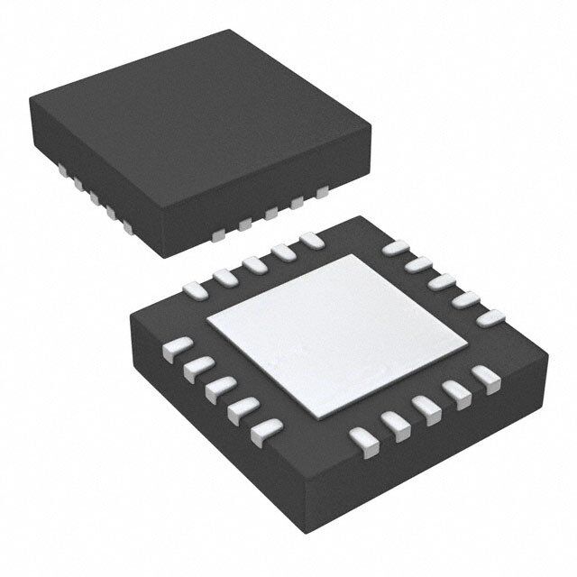
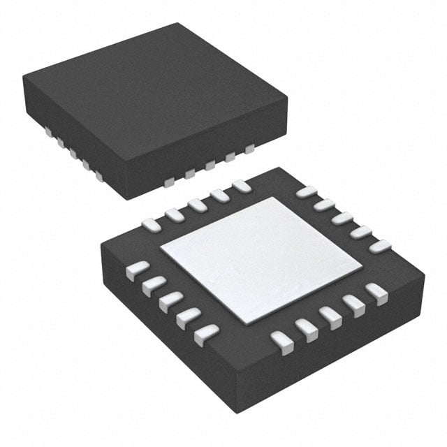
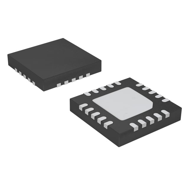
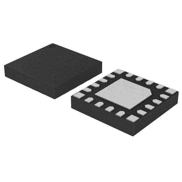
| 描述 | IC RF VALUE LINE TXRX 20QFN射频接收器 Value Line Receiver |
| 产品分类 | |
| 品牌 | Texas Instruments |
| 产品手册 | http://www.ti.com/litv/swrs108a |
| 产品图片 |
|
| rohs | 符合RoHS无铅 / 符合限制有害物质指令(RoHS)规范要求 |
| 产品系列 | RF集成电路,射频接收器,Texas Instruments CC113LRGPR- |
| 数据手册 | |
| 产品型号 | CC113LRGPR |
| PCN设计/规格 | |
| 产品种类 | 射频接收器 |
| 供应商器件封装 | 20-QFN(4x4) |
| 其它名称 | 296-35720-1 |
| 制造商产品页 | http://www.ti.com/general/docs/suppproductinfo.tsp?distId=10&orderablePartNumber=CC113LRGPR |
| 包装 | 剪切带 (CT) |
| 商标 | Texas Instruments |
| 天线连接器 | PCB,表面贴装 |
| 存储容量 | - |
| 安装风格 | SMD/SMT |
| 封装 | Reel |
| 封装/外壳 | 20-VFQFN 裸露焊盘 |
| 封装/箱体 | VQFN-20 |
| 工作温度 | -40°C ~ 85°C |
| 工作电源电压 | 3 V |
| 工作频率 | 300 MHz to 348 MHz, 387 MH to 464 MHz, 779 MHz to 928 MHz |
| 工厂包装数量 | 3000 |
| 带宽 | 812 kHz |
| 应用 | 通用 |
| 数据接口 | PCB,表面贴装 |
| 数据速率(最大值) | 600kbps |
| 最大工作温度 | + 85 C |
| 最小工作温度 | - 40 C |
| 标准包装 | 1 |
| 灵敏度 | -116dBm |
| 特性 | - |
| 电压-电源 | 1.8 V ~ 3.6 V |
| 电流-接收 | 17.1mA |
| 电源电压-最大 | 3.6 V |
| 电源电压-最小 | 1.8 V |
| 电源电流 | 14 mA |
| 类型 | Receiver |
| 系列 | CC113L |
| 调制或协议 | FSK,GFSK,OOK |
| 频率 | 315MHz,433MHz,868MHz,915MHz |


- 商务部:美国ITC正式对集成电路等产品启动337调查
- 曝三星4nm工艺存在良率问题 高通将骁龙8 Gen1或转产台积电
- 太阳诱电将投资9.5亿元在常州建新厂生产MLCC 预计2023年完工
- 英特尔发布欧洲新工厂建设计划 深化IDM 2.0 战略
- 台积电先进制程称霸业界 有大客户加持明年业绩稳了
- 达到5530亿美元!SIA预计今年全球半导体销售额将创下新高
- 英特尔拟将自动驾驶子公司Mobileye上市 估值或超500亿美元
- 三星加码芯片和SET,合并消费电子和移动部门,撤换高东真等 CEO
- 三星电子宣布重大人事变动 还合并消费电子和移动部门
- 海关总署:前11个月进口集成电路产品价值2.52万亿元 增长14.8%


PDF Datasheet 数据手册内容提取
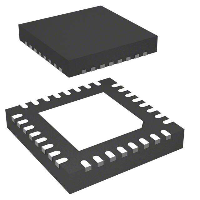
Product Sample & Technical Tools & Support & Folder Buy Documents Software Community CC113L SWRS108B–MAY2011–REVISEDJUNE2014 CC113L Value Line Receiver 1 Device Overview 1.1 Features 1 • RFPerformance • General – ReceiveSensitivityDownto −116dBmat – FewExternalComponents;CompletelyOn-chip 0.6kbps FrequencySynthesizer,NoExternalFiltersor – ProgrammableDataRatefrom0.6to600kbps RFSwitchNeeded – FrequencyBands:300–348MHz, – GreenPackage:RoHSCompliantandNo 387–464MHz,and779–928MHz AntimonyorBromine – 2-FSK,4-FSK,GFSK,MSK,andOOK – SmallSize(QLP4-x4-mmPackage,20Pins) Supported – SuitedforSystemsTargetingCompliancewith • DigitalFeatures EN300220(Europe)andFCCCFRPart15 (US) – FlexibleSupportforPacketOrientedSystems – SupportforAsynchronousandSynchronous – On-chipSupportforSyncWordDetection, SerialTransmitModeforBackward FlexiblePacketLength,andAutomaticCRC CompatibilitywithExistingRadio Calculation CommunicationProtocols • Low-PowerFeatures – 200-nASleepModeCurrentConsumption – FastStartupTime;240 μsFromSleeptoRX Mode – 64-ByteRXFIFO 1.2 Applications • UltraLow-PowerWirelessApplicationsOperating • IndustrialMonitoringandControl inthe315-,433-,868-,915-MHzISMorSRD • RemoteControls Bands • Toys • WirelessAlarmandSecuritySystems • HomeandBuildingAutomation 1.3 Description The CC113L is a cost optimized sub-1 GHz RF receiver for the 300–348 MHz, 387–464 MHz, and 779–928 MHz frequency bands. The circuit is based on the popular CC1101 RF transceiver, and RF performance characteristics are identical. The CC115L transmitter together with the CC113L receiver enablealow-costRFlink. The RF receiver is integrated with a highly configurable baseband demodulator. The modem supports variousmodulationformatsandhasaconfigurabledatarateupto600kbps. The CC113L provides extensive hardware support for packet handling, data buffering, and burst transmissions. The main operating parameters and the 64-byte receive FIFO of CC113L can be controlled through a serial peripheral interface (SPI). In a typical system, the CC113L will be used together with a microcontrollerandafewadditionalpassivecomponents. DeviceInformation(1) PARTNUMBER PACKAGE BODYSIZE CC113LRGP QFN(20) 4.00mm×4.00mm (1) Formoreinformationonthesedevices,seeSection8,MechanicalPackagingandOrderable Information. 1 AnIMPORTANTNOTICEattheendofthisdatasheetaddressesavailability,warranty,changes,useinsafety-criticalapplications, intellectualpropertymattersandotherimportantdisclaimers.PRODUCTIONDATA.
CC113L SWRS108B–MAY2011–REVISEDJUNE2014 www.ti.com 1.4 Functional Block Diagram Figure1-1showsafunctionalblockdiagramofthedevice. Radio Control SCLK RF_P ADC U SO (GDO1) LNA C M RF_N 090 ASFDYRCNETQH Demodulator Packet Handler RX FIFO gitalInterface to CSGISDnO0 Di GDO2 BIAS XOSC RBIAS XOSC_Q1 XOSC_Q2 Figure1-1.FunctionalBlockDiagram 2 DeviceOverview Copyright©2011–2014,TexasInstrumentsIncorporated SubmitDocumentationFeedback ProductFolderLinks:CC113L
CC113L www.ti.com SWRS108B–MAY2011–REVISEDJUNE2014 Table of Contents 1 DeviceOverview......................................... 1 Decision............................................. 26 .............................................. ................. 1.1 Features 1 5.10 PacketHandlingHardwareSupport 27 ........................................... ................................. 1.2 Applications 1 5.11 ModulationFormats 31 ............................................ ............... 1.3 Description 1 5.12 ReceivedSignalQualifiersandRSSI 32 ............................ ........................................ 1.4 FunctionalBlockDiagram 2 5.13 RadioControl 36 2 Revision History......................................... 4 5.14 RXFIFO............................................. 41 3 TerminalConfigurationandFunctions.............. 5 5.15 FrequencyProgramming............................ 43 .......................................... ................................................. 3.1 PinDiagram 5 5.16 VCO 44 ................................... .................................. 3.2 SignalDescriptions 6 5.17 VoltageRegulators 44 4 Specifications ............................................ 7 5.18 GeneralPurposeandTestOutputControlPins.... 45 .......................... .. 4.1 AbsoluteMaximumRatings 7 5.19 AsynchronousandSynchronousSerialOperation 47 ..................................... .............. 4.2 Handling Ratings 7 5.20 SystemConsiderationandGuidelines 48 ................ ............................. 4.3 RecommendedOperatingConditions 7 5.21 ConfigurationRegisters 49 .............................. .............. 4.4 General Characteristics 7 5.22 DevelopmentKitOrderingInformation 69 4.5 CurrentConsumption................................. 8 6 Applications,Implementation,andLayout........ 70 .................................. ........................................ 4.6 RFReceiveSection 9 6.1 BiasResistor 70 .................................... ............................. 4.7 CrystalOscillator 11 6.2 BalunandRFMatching 70 ............. ............................................... 4.8 FrequencySynthesizerCharacteristics 12 6.3 Crystal 73 .................................. .................................... 4.9 DCCharacteristics 12 6.4 Reference Signal 73 .................................... ........................... 4.10 Power-OnReset 12 6.5 PowerSupplyDecoupling 73 ............................. ..................... 4.11 Thermal Characteristics 12 6.6 PCBLayoutRecommendations 73 4.12 TypicalCharacteristics.............................. 13 7 DeviceandDocumentationSupport............... 75 5 DetailedDescription................................... 15 7.1 DeviceSupport...................................... 75 ............................................ ............................. 5.1 Overview 15 7.2 DocumentationSupport 76 ........................... .......................................... 5.2 FunctionalBlockDiagram 15 7.3 Trademarks 76 ............................. ..................... 5.3 ConfigurationOverview 16 7.4 ElectrostaticDischargeCaution 77 .............................. ............................... 5.4 ConfigurationSoftware 18 7.5 ExportControlNotice 77 ..... ............................................. 5.5 4-wireSerialConfigurationandDataInterface 19 7.6 Glossary 77 ..... ................................ 5.6 MicrocontrollerInterfaceandPinConfiguration 23 7.7 AdditionalAcronyms 77 5.7 DataRateProgramming............................ 24 8 MechanicalPackagingandOrderable ................. Information.............................................. 79 5.8 ReceiverChannelFilterBandwidth 25 .............................. 5.9 Demodulator,SymbolSynchronizer,andData 8.1 PackagingInformation 79 Copyright©2011–2014,TexasInstrumentsIncorporated TableofContents 3 SubmitDocumentationFeedback ProductFolderLinks:CC113L
CC113L SWRS108B–MAY2011–REVISEDJUNE2014 www.ti.com 2 Revision History NOTE:Pagenumbersforpreviousrevisionsmaydifferfrompagenumbersinthecurrentversion. ChangesfromRevisionA(February2013)toRevisionB Page • ChangedformatofdatasheettostandardTIformat. ........................................................................... 1 • Changedresetvaluefrom0x08to0x18......................................................................................... 66 • ChangedthepackagedesignatorfromRTKtoRGP .......................................................................... 79 4 RevisionHistory Copyright©2011–2014,TexasInstrumentsIncorporated SubmitDocumentationFeedback ProductFolderLinks:CC113L
CC113L www.ti.com SWRS108B–MAY2011–REVISEDJUNE2014 3 Terminal Configuration and Functions 3.1 Pin Diagram The CC113L pinout is shown in Figure 3-1 and Table 3-1. See Section 5.18 for details on the I/O configuration. D R A S D U A D N G BI N SI G D R G 20 19 18 17 16 SCLK1 15 AVDD SO(GDO1)2 14AVDD GDO23 13RF_N DVDD4 12 RF_P DCOUPL5 11 AVDD GND 6 7 8 9 10 Exposed die G C X A X D S O V O attach pad O n S D S 0 C D C _ _ Q Q 1 2 Figure3-1.PinoutTopView NOTE The exposed die attach pad must be connected to a solid ground plane as this is the main groundconnectionforthechip Copyright©2011–2014,TexasInstrumentsIncorporated TerminalConfigurationandFunctions 5 SubmitDocumentationFeedback ProductFolderLinks:CC113L
CC113L SWRS108B–MAY2011–REVISEDJUNE2014 www.ti.com 3.2 Signal Descriptions Table3-1.SignalDescriptions PinNo. PinName PinType Description 1 SCLK Digital Serialconfigurationinterface,clockinput Input 2 SO Digital Serialconfigurationinterface,dataoutput (GDO1) Output OptionalgeneraloutputpinwhenCSnishigh 3 GDO2 Digital Digitaloutputpinforgeneraluse: Output • Testsignals • FIFOstatussignals • Clockoutput,down-dividedfromXOSC • SerialoutputRXdata 4 DVDD Power 1.8-3.6VdigitalpowersupplyfordigitalI/Osandforthedigitalcorevoltageregulator (Digital) 5 DCOUPL Power 1.6-2.0Vdigitalpowersupplyoutputfordecoupling (Digital) NOTE: This pin is intended for use with the CC113L only. It can not be used to provide supply voltagetootherdevices 6 GDO0 DigitalI/O Digitaloutputpinforgeneraluse: • Testsignals • FIFOstatussignals • Clockoutput,down-dividedfromXOSC • SerialoutputRXdata 7 CSn Digital Serialconfigurationinterface,chipselect Input 8 XOSC_Q1 AnalogI/O Crystaloscillatorpin1,orexternalclockinput 9 AVDD Power 1.8-3.6Vanalogpowersupplyconnection (Analog) 10 XOSC_Q2 AnalogI/O Crystaloscillatorpin2 11 AVDD Power 1.8-3.6Vanalogpowersupplyconnection (Analog) 12 RF_P RFI/O PositiveRFinputsignaltoLNAinreceivemode 13 RF_N RFI/O NegativeRFinputsignaltoLNAinreceivemode 14 AVDD Power 1.8-3.6Vanalogpowersupplyconnection (Analog) 15 AVDD Power 1.8-3.6Vanalogpowersupplyconnection (Analog) 16 GND Ground Analoggroundconnection (Analog) 17 RBIAS AnalogI/O Externalbiasresistorforreferencecurrent 18 DGUARD Power Powersupplyconnectionfordigitalnoiseisolation (Digital) 19 GND Ground Groundconnectionfordigitalnoiseisolation (Digital) 20 SI Digital Serialconfigurationinterface,datainput Input 6 TerminalConfigurationandFunctions Copyright©2011–2014,TexasInstrumentsIncorporated SubmitDocumentationFeedback ProductFolderLinks:CC113L
CC113L www.ti.com SWRS108B–MAY2011–REVISEDJUNE2014 4 Specifications 4.1 Absolute Maximum Ratings Undernocircumstancesmusttheabsolutemaximumratingsbeviolated.Stressexceedingoneormoreofthelimitingvalues maycausepermanentdamagetothedevice. Parameter Min Max Units Condition Supplyvoltage –0.3 3.9 V Allsupplypinsmusthavethesamevoltage VDD+0.3, Voltageonanydigitalpin –0.3 V max3.9 VoltageonthepinsRF_P,RF_N, –0.3 2.0 V DCOUPL,RBIAS Voltageramp-uprate 120 kV/µs InputRFlevel +10 dBm 4.2 Handling Ratings Parameter MIN MAX UNIT Storagetemperature (default) –50 150 °C range,T stg ESDStressVoltage, HumanBodyModel(HBM),perANSI/ESDA/JEDECJS001(1) 750 V VESD ChargedDeviceModel(CDM),perJJESD22-C101(2) 400 V (1) JEDECdocumentJEP155statesthat500-VHBMallowssafemanufacturingwithastandardESDcontrolprocess. (2) JEDECdocumentJEP157statesthat250-VHBMallowssafemanufacturingwithastandardESDcontrolprocess. 4.3 Recommended Operating Conditions Parameter Min Max Unit Condition Operatingtemperature –40 85 °C Operatingsupplyvoltage 1.8 3.6 V Allsupplypinsmusthavethesamevoltage 4.4 General Characteristics Parameter Min Typ Max Unit Condition 300 348 MHz Ifusinga27MHzcrystal,thelowerfrequencylimitforthis Frequencyrange 387 464 MHz bandis392MHz 779 928 MHz 0.6 500 kBaud 2-FSK 0.6 250 kBaud GFSKandOOK Datarate 0.6 300 kBaud 4-FSK(thedatarateinkbpswillbetwicethebaudrate) OptionalManchesterencoding(thedatarateinkbpswillbe halfthebaudrate) Copyright©2011–2014,TexasInstrumentsIncorporated Specifications 7 SubmitDocumentationFeedback ProductFolderLinks:CC113L
CC113L SWRS108B–MAY2011–REVISEDJUNE2014 www.ti.com 4.5 Current Consumption T =25°C,VDD=3.0Vifnothingelsestated.AllmeasurementresultsareobtainedusingSWRR046andSWRR045. A Reducedcurrentsettings,MDMCFG2.DEM_DCFILT_OFF=1,givesaslightlylowercurrentconsumptionatthecostofa reductioninsensitivity.SeeSection4.6foradditionaldetailsoncurrentconsumptionandsensitivity. Parameter Min Typ Max Unit Condition Voltageregulatortodigitalpartoff,registervaluesretained(SLEEPstate).AllGDOpinsprogrammedto0x2F 0.2 1 µA (HWto0) Currentconsumption inpowerdown Voltageregulatortodigitalpartoff,registervaluesretained,XOSCrunning(SLEEPstatewith 100 µA modes MCSM0.OSC_FORCE_ONset) 165 µA Voltageregulatortodigitalparton,allothermodulesinpowerdown(XOFFstate) 1.7 mA Onlyvoltageregulatortodigitalpartandcrystaloscillatorrunning(IDLEstate) Currentconsumption 8.4 mA ThecurrentconsumptionfortheintermediatestateswhengoingfromIDLEtoRX,includingthecalibrationstate 15.4 mA Receivemode,1.2kBaud,reducedcurrent,inputatsensitivitylimit 14.4 mA Receivemode,1.2kBaud,registersettingsoptimizedforreducedcurrent,inputwellabovesensitivitylimit Currentconsumption, 15.2 mA Receivemode,38.4kBaud,registersettingsoptimizedforreducedcurrent,inputatsensitivitylimit 315MHz 14.3 mA Receivemode,38.4kBaud,registersettingsoptimizedforreducedcurrent,inputwellabovesensitivitylimit 16.5 mA Receivemode,250kBaud,registersettingsoptimizedforreducedcurrent,inputatsensitivitylimit 15.1 mA Receivemode,250kBaud,registersettingsoptimizedforreducedcurrent,inputwellabovesensitivitylimit 16.0 mA Receivemode,1.2kBaud,registersettingsoptimizedforreducedcurrent,inputatsensitivitylimit 15.0 mA Receivemode,1.2kBaud,registersettingsoptimizedforreducedcurrent,inputwellabovesensitivitylimit Currentconsumption, 15.7 mA Receivemode,38.4kBaud,registersettingsoptimizedforreducedcurrent,inputatsensitivitylimit 433MHz 15.0 mA Receivemode,38.4kBaud,registersettingsoptimizedforreducedcurrent,inputwellabovesensitivitylimit 17.1 mA Receivemode,250kBaud,registersettingsoptimizedforreducedcurrent,inputatsensitivitylimit 15.7 mA Receivemode,250kBaud,registersettingsoptimizedforreducedcurrent,inputwellabovesensitivitylimit Receivemode,1.2kBaud,registersettingsoptimizedforreducedcurrent,inputatsensitivitylimit. 15.7 mA SeeFigure4-1throughFigure4-3forcurrentconsumptionwithregistersettingsoptimizedforsensitivity. Receivemode,1.2kBaud,registersettingsoptimizedforreducedcurrent,inputwellabovesensitivitylimit. 14.7 mA SeeFigure4-1throughFigure4-3forcurrentconsumptionwithregistersettingsoptimizedforsensitivity. Receivemode,38.4kBaud,registersettingsoptimizedforreducedcurrent,inputatsensitivitylimit. 15.6 mA Currentconsumption, SeeFigure4-1throughFigure4-3forcurrentconsumptionwithregistersettingsoptimizedforsensitivity. 868/915MHz Receivemode,38.4kBaud,registersettingsoptimizedforreducedcurrent,inputwellabovesensitivitylimit. 14.6 mA SeeFigure4-1throughFigure4-3forcurrentconsumptionwithregistersettingsoptimizedforsensitivity. Receivemode,250kBaud,registersettingsoptimizedforreducedcurrent,inputatsensitivitylimit. 16.9 mA SeeFigure4-1throughFigure4-3forcurrentconsumptionwithregistersettingsoptimizedforsensitivity. Receivemode,250kBaud,registersettingsoptimizedforreducedcurrent,inputwellabovesensitivitylimit. 15.6 mA SeeFigure4-1throughFigure4-3forcurrentconsumptionwithregistersettingsoptimizedforsensitivity. 4.5.1 Typical RX Current Consumption over Temperature and Input Power Level, 868/915 MHz SeeSection4.12.1. 8 Specifications Copyright©2011–2014,TexasInstrumentsIncorporated SubmitDocumentationFeedback ProductFolderLinks:CC113L
CC113L www.ti.com SWRS108B–MAY2011–REVISEDJUNE2014 4.6 RF Receive Section T = 25°C, VDD = 3.0 V if nothing else stated. All measurement results are obtained using SWRR046 and A SWRR045. Parameter Min Typ Max Unit Condition Digitalchannelfilter Userprogrammable.Thebandwidthlimitsareproportionalto 58 812 kHz bandwidth crystalfrequency(givenvaluesassumea26.0MHzcrystal) 25MHz-1GHz –68 –57 dBm (MaximumfigureistheETSIEN300220V2.3.1limit) Above1GHz Spuriousemissions (MaximumfigureistheETSIEN300220V2.3.1limit) –66 –47 dBm Typicalradiatedspuriousemissionis–49dBmmeasuredatthe VCOfrequency Serialoperation.Timefromstartofreceptionuntildatais RXlatency 9 bit availableonthereceiverdataoutputpinisequalto9bit 315MHz 1.2kBauddatarate,sensitivityoptimized,MDMCFG2.DEM_DCFILT_OFF=0 (2-FSK,1%packeterrorrate,20bytespacketlength,5.2kHzdeviation,58kHzdigitalchannelfilterbandwidth) Sensitivitycanbetradedforcurrentconsumptionbysetting MDMCFG2.DEM_DCFILT_OFF=1.Thetypicalcurrent Receiversensitivity –111 dBm consumptionisthenreducedfrom17.2mAto15.4mAatthe sensitivitylimit.Thesensitivityistypicallyreducedto-109dBm 433MHz 0.6kBauddatarate,sensitivityoptimized,MDMCFG2.DEM_DCFILT_OFF=0 (GFSK,1%packeterrorrate,20bytespacketlength,14.3kHzdeviation,58kHzdigitalchannelfilterbandwidth) Receiversensitivity –116 dBm 1.2kBauddatarate,sensitivityoptimized,MDMCFG2.DEM_DCFILT_OFF=0 GFSK,1%packeterrorrate,20bytespacketlength,5.2kHzdeviation,58kHzdigitalchannelfilterbandwidth) Sensitivitycanbetradedforcurrentconsumptionbysetting MDMCFG2.DEM_DCFILT_OFF=1.Thetypicalcurrent Receiversensitivity –112 dBm consumptionisthenreducedfrom18.0mAto16.0mAatthe sensitivitylimit.Thesensitivityistypicallyreducedto–110dBm 38.4kBauddatarate,sensitivityoptimized,MDMCFG2.DEM_DCFILT_OFF=0 (GFSK,1%packeterrorrate,20bytespacketlength,20kHzdeviation,100kHzdigitalchannelfilterbandwidth) Receiversensitivity –104 dBm 250kBauddatarate,sensitivityoptimized,MDMCFG2.DEM_DCFILT_OFF=0 (GFSK,1%packeterrorrate,20bytespacketlength,127kHzdeviation,540kHzdigitalchannelfilterbandwidth) Receiversensitivity –95 dBm 868/915MHz 1.2kBauddatarate,sensitivityoptimized,MDMCFG2.DEM_DCFILT_OFF=0 (GFSK,1%packeterrorrate,20bytespacketlength,5.2kHzdeviation,58kHzdigitalchannelfilterbandwidth) Sensitivitycanbetradedforcurrentconsumptionbysetting MDMCFG2.DEM_DCFILT_OFF=1.Thetypicalcurrent Receiversensitivity –112 dBm consumptionisthenreducedfrom17.7mAto15.7mAat sensitivitylimit.Thesensitivityistypicallyreducedto–109dBm Saturation –14 dBm FIFOTHR.CLOSE_IN_RX=0.SeemoreinDN010SWRA147 Desiredchannel3dBabovethesensitivitylimit. Adjacentchannelrejection 100kHzchannelspacing 37 dB ±100kHzoffset SeeFigure4-4andFigure4-5forselectivityperformanceat otheroffsetfrequencies IFfrequency152kHz Imagechannelrejection 31 dB Desiredchannel3dBabovethesensitivitylimit Blocking Desiredchannel3dBabovethesensitivitylimit SeeFigure4-4andFigure4-5forblockingperformanceatother ±2MHzoffset –50 dBm offsetfrequencies ±10MHzoffset –40 dBm Copyright©2011–2014,TexasInstrumentsIncorporated Specifications 9 SubmitDocumentationFeedback ProductFolderLinks:CC113L
CC113L SWRS108B–MAY2011–REVISEDJUNE2014 www.ti.com Parameter Min Typ Max Unit Condition 38.4kBauddatarate,sensitivityoptimized,MDMCFG2.DEM_DCFILT_OFF=0 (GFSK,1%packeterrorrate,20bytespacketlength,20kHzdeviation,100kHzdigitalchannelfilterbandwidth) Receiversensitivity Sensitivitycanbetradedforcurrentconsumptionbysetting MDMCFG2.DEM_DCFILT_OFF=1.Thetypicalcurrent –104 dBm consumptionisthenreducedfrom17.7mAto15.6mAatthe sensitivitylimit.Thesensitivityistypicallyreducedto-102dBm Saturation –16 dBm FIFOTHR.CLOSE_IN_RX=0.SeemoreinDN010SWRA147 Adjacentchannelrejection Desiredchannel3dBabovethesensitivitylimit. 200kHzchannelspacing –200kHzoffset 12 dB SeeFigure4-6andFigure4-7forblockingperformanceatother +200kHzoffset 25 dB offsetfrequencies Imagechannelrejection IFfrequency152kHz 23 dB Desiredchannel3dBabovethesensitivitylimit Blocking Desiredchannel3dBabovethesensitivitylimit SeeFigure4-6andFigure4-7forblockingperformanceatother ±2MHzoffset –50 dBm offsetfrequencies ±10MHzoffset –40 dBm 250kBauddatarate,sensitivityoptimized,MDMCFG2.DEM_DCFILT_OFF=0 (GFSK,1%packeterrorrate,20bytespacketlength,127kHzdeviation,540kHzdigitalchannelfilterbandwidth) Sensitivitycanbetradedforcurrentconsumptionbysetting MDMCFG2.DEM_DCFILT_OFF=1.Thetypicalcurrent Receiversensitivity –95 dBm consumptionisthenreducedfrom18.9mAto16.9mAatthe sensitivitylimit.Thesensitivityistypicallyreducedto-91dBm Saturation –17 dBm FIFOTHR.CLOSE_IN_RX=0.SeemoreinDN010SWRA147 Desiredchannel3dBabovethesensitivitylimit. 750-kHzchannelspacing Adjacentchannelrejection 25 dB SeeFigure4-8andFigure4-9forblockingperformanceatother offsetfrequencies IFfrequency304kHz Imagechannelrejection 14 dB Desiredchannel3dBabovethesensitivitylimit Blocking Desiredchannel3dBabovethesensitivitylimit SeeFigure4-8andFigure4-9forblockingperformanceatother ±2MHzoffset –50 dBm offsetfrequencies ±10MHzoffset –40 dBm 4-FSK,125kBauddatarate(250kbps),sensitivityoptimized,MDMCFG2.DEM_DCFILT_OFF=0 (1%packeterrorrate,20bytespacketlength,127kHzdeviation,406kHzdigitalchannelfilterbandwidth) Receiversensitivity –96 dBm 4-FSK,250kBauddatarate(500kbps),sensitivityoptimized,MDMCFG2.DEM_DCFILT_OFF=0 (1%packeterrorrate,20bytespacketlength,254kHzdeviation,812kHzdigitalchannelfilterbandwidth Receiversensitivity –91 dBm 4-FSK,300kBauddatarate(600kbps),sensitivityoptimized,MDMCFG2.DEM_DCFILT_OFF=0 (1%packeterrorrate,20bytespacketlength,228kHzdeviation,812kHzdigitalchannelfilterbandwidth) Receiversensitivity –89 dBm 10 Specifications Copyright©2011–2014,TexasInstrumentsIncorporated SubmitDocumentationFeedback ProductFolderLinks:CC113L
CC113L www.ti.com SWRS108B–MAY2011–REVISEDJUNE2014 4.6.1 Typical Sensitivity over Temperature and Supply Voltage, 868 MHz, Sensitivity Optimized Setting SupplyVoltage SupplyVoltage SupplyVoltage VDD=1.8V VDD=3.0V VDD=3.6V Temperature[°C] –40 25 85 –40 25 85 –40 25 85 Sensitivity[dBm]1.2kBaud –113 –112 –110 –113 –112 –110 –113 –112 –110 Sensitivity[dBm]38.4kBaud –105 –104 –102 –105 –104 –102 –105 –104 –102 Sensitivity[dBm]250kBaud –97 –96 –92 –97 –95 –92 –97 –94 –92 Sensitivity[dBm]500kBaud –91 –90 –86 –91 –90 –86 –91 –90 –86 4.6.2 Typical Sensitivity over Temperature and Supply Voltage, 915 MHz, Sensitivity Optimized Setting SupplyVoltage SupplyVoltage SupplyVoltage VDD=1.8V VDD=3.0V VDD=3.6V Temperature[°C] –40 25 85 –40 25 85 –40 25 85 Sensitivity[dBm]1.2kBaud –113 –112 –110 –113 –112 –110 –113 –112 –110 Sensitivity[dBm]38.4kBaud –105 –104 –102 –104 –104 –102 –105 –104 –102 Sensitivity[dBm]250kBaud –97 –94 –92 –97 –95 –92 –97 –95 –92 Sensitivity[dBm]500kBaud –91 –89 –86 –91 –90 –86 –91 –89 –86 4.6.3 Blocking and Selectivity SeeSection4.12.2. 4.7 Crystal Oscillator T =25°C,VDD=3.0Vifnothingelseisstated.AllmeasurementresultsobtainedusingSWRR046andSWRR045. A Parameter Min Typ Max Unit Condition Forcompliancewithmodulationbandwidthrequirementsunder EN300220V2.3.1inthe863to870MHzfrequencyrangeitis Crystalfrequency 26 26 27 MHz recommendedtousea26-MHzcrystalforfrequenciesbelow 869MHzanda27MHzcrystalforfrequenciesabove869MHz. Thisisthetotaltoleranceincludinga)initialtolerance,b)crystal loading,c)aging,andd)temperaturedependence.The Tolerance ±40 ppm acceptablecrystaltolerancedependsonRFfrequencyand channelspacing/bandwidth. Loadcapacitance 10 13 20 pF Simulatedoveroperatingconditions ESR 100 Ω Thisparameteristoalargedegreecrystaldependent. Start-uptime 150 µs MeasuredonSWRR046andSWRR045usingcrystalAT-41CD2 fromNDK Copyright©2011–2014,TexasInstrumentsIncorporated Specifications 11 SubmitDocumentationFeedback ProductFolderLinks:CC113L
CC113L SWRS108B–MAY2011–REVISEDJUNE2014 www.ti.com 4.8 Frequency Synthesizer Characteristics T =25°C,VDD=3.0Vifnothingelseisstated.AllmeasurementresultsareobtainedusingSWRR046andSWRR045.Min A figuresaregivenusinga27-MHzcrystal.Typandmaxfiguresaregivenusinga26-MHzcrystal. Parameter Min Typ Max Unit Condition Programmedfrequency 397 F /216 412 Hz 26-to27-MHzcrystal.Theresolution(inHz)is resolution XOSC equalforallfrequencybands Givenbycrystalused.Requiredaccuracy (includingtemperatureandaging)dependson Synthesizerfrequencytolerance ±40 ppm frequencybandandchannelbandwidth/ spacing RFcarrierphasenoise –92 dBc/Hz at50kHzoffsetfromcarrier RFcarrierphasenoise –92 dBc/Hz at100kHzoffsetfromcarrier RFcarrierphasenoise –92 dBc/Hz at200kHzoffsetfromcarrier RFcarrierphasenoise –98 dBc/Hz at500kHzoffsetfromcarrier RFcarrierphasenoise –107 dBc/Hz at1MHzoffsetfromcarrier RFcarrierphasenoise –113 dBc/Hz at2MHzoffsetfromcarrier RFcarrierphasenoise –119 dBc/Hz at5MHzoffsetfromcarrier RFcarrierphasenoise –129 dBc/Hz at10MHzoffsetfromcarrier TimefromleavingtheIDLEstateuntilarrivingin PLLturn-onorhoptime 72 75 75 µs theRXstate,whennotperformingcalibration. (SeeTable5-12) Crystaloscillatorrunning. PLLcalibrationtime Calibrationcanbeinitiatedmanuallyor 685 712 724 µs (SeeTable5-13) automaticallybeforeenteringorafterleavingRX 4.9 DC Characteristics T =25°Cifnothingelsestated. A DigitalInputs/Outputs Min Max Unit Condition Logic"0"inputvoltage 0 0.7 V Logic"1"inputvoltage VDD–0.7 VDD V Logic"0"outputvoltage 0 0.5 V Forupto4mAoutputcurrent Logic"1"outputvoltage VDD–0.3 VDD V Forupto4mAoutputcurrent Logic"0"inputcurrent N/A –50 nA Inputequals0V Logic"1"inputcurrent N/A 50 nA InputequalsVDD 4.10 Power-On Reset ForproperPower-On-ResetfunctionalitythepowersupplyshouldcomplywiththerequirementsinSection4.10.Otherwise, thechipshouldbeassumedtohaveunknownstateuntiltransmittinganSRESstrobeovertheSPIinterface.See Section5.13.1,Power-OnStart-UpSequence,forfurtherdetails. Parameter Min Typ Max Unit Condition Power-upramp-uptime 5 ms From0Vuntilreaching1.8V Powerofftime 1 ms Minimumtimebetweenpower-onandpower-off 4.11 Thermal Characteristics(1) NAME DESCRIPTION QFN(°C/W) R Junction-to-ambientthermalresistance 47 θJA R Junction-to-case(top)thermalresistance 45 θJC(top) R Junction-to-boardthermalresistance 13.6 θJB R Junction-to-case(bottom)thermalresistance 5.12 θJC(bot) (1) Formoreinformationabouttraditionalandnewthermalmetrics,seetheICPackageThermalMetricsapplicationreport,SPRA953. 12 Specifications Copyright©2011–2014,TexasInstrumentsIncorporated SubmitDocumentationFeedback ProductFolderLinks:CC113L
CC113L www.ti.com SWRS108B–MAY2011–REVISEDJUNE2014 4.12 Typical Characteristics 4.12.1 Typical Characteristics, RX Current Consumption 17.8 17.8 25°C ±40ƒC 17.6 ±40ƒC 17.6 25°C 85°C 85°C 17.4 17.4 A) 17.2 A) 17.2 m m nt (17.0 nt (17.0 e e Curr16.8 Curr16.8 16.6 16.6 16.4 16.4 16.2 16.2 ±110 ±90 ±70 ±50 ±30 ±10 ±100 ±80 ±60 ±40 ±20 Input Power Level (dBm) Input Power Level (dBm) C001 C002 Figure4-1.TypicalRXCurrentConsumptionOverTemperature Figure4-2.TypicalRXCurrentConsumptionOverTemperature andInputPowerLevel,868or915MHz,SensitivityOptimized andInputPowerLevel,868or915MHz,SensitivityOptimized Setting–1.2kBaudGFSK Setting–38.4kBaudGFSK 19.5 ±40ƒC 25°C 19.0 85°C A) 18.5 m nt (18.0 e urr C17.5 17.0 16.5 ±100 ±80 ±60 ±40 ±20 Input Power Level (dBm) C003 Figure4-3.TypicalRXCurrentConsumptionOverTemperatureandInputPowerLevel,868or915MHz,SensitivityOptimized Setting–250kBaudGFSK Copyright©2011–2014,TexasInstrumentsIncorporated Specifications 13 SubmitDocumentationFeedback ProductFolderLinks:CC113L
CC113L SWRS108B–MAY2011–REVISEDJUNE2014 www.ti.com 4.12.2 Typical Characteristics, Blocking and Selectivity 80 60 70 50 60 50 40 ng (dB) 3400 vity (dB) 30 Blocki 20 Selecti 20 10 10 0 0 ±10 ±20 ±10 ±40 ±30 ±20 ±10 0 10 20 30 40 ±1.0 ±0.8 ±0.6 ±0.4 ±0.2 0.0 0.2 0.4 0.6 0.8 1.0 Offset (MHz) Offset (MHz) C004 C005 Figure4-4.TypicalBlockingat1.2kBaudDataRate,868.3MHz, Figure4-5.TypicalSelectivityat1.2kBaudDataRate,868.3 GFSK,5.2kHzDeviation.IFis152.3kHzandtheDigitalChannel MHz,GFSK,5.2kHzDeviation.IFis152.3kHzandtheDigital FilterBandwidthis58kHz ChannelFilterBandwidthis58kHz 70 50 60 40 50 30 ng (dB) 3400 vity (dB) 20 Blocki 1200 Selecti 10 0 0 ±10 ±10 ±20 ±20 ±40 ±30 ±20 ±10 0 10 20 30 40 ±1.0 ±0.8 ±0.6 ±0.4 ±0.2 0.0 0.2 0.4 0.6 0.8 1.0 Offset (MHz) Offset (MHz) C006 C007 Figure4-6.TypicalBlockingat38.4kBaudDataRate,868MHz, Figure4-7.TypicalSelectivityat38.4kBaudDataRate,868MHz, GFSK,20kHzDeviation.IFis152.3kHzandtheDigitalChannel GFSK,20kHzDeviation.IFis152.3kHzandtheDigitalChannel FilterBandwidthis100kHz FilterBandwidthis100kHz 60 50 50 40 40 30 ng (dB) 2300 vity (dB) 20 Blocki 10 Selecti 10 0 0 ±10 ±10 ±20 ±20 ±40 ±30 ±20 ±10 0 10 20 30 40 ±2.0 ±1.5 ±1.0 ±0.5 0.0 0.5 1.0 1.5 2.0 Offset (MHz) Offset (MHz) C008 C009 Figure4-8.TypicalBlockingat250kBaudDataRate,868MHz, Figure4-9.TypicalSelectivityat250kBaudDataRate,868MHz, GFSK,IFis304kHzandtheDigitalChannelFilterBandwidthis GFSK,IFis304kHzandtheDigitalChannelFilterBandwidthis 540kHz 540kHz 14 Specifications Copyright©2011–2014,TexasInstrumentsIncorporated SubmitDocumentationFeedback ProductFolderLinks:CC113L
CC113L www.ti.com SWRS108B–MAY2011–REVISEDJUNE2014 5 Detailed Description 5.1 Overview CC113L features a low-IF receiver. The received RF signal is amplified by the low-noise amplifier (LNA) and down-converted in quadrature (I and Q) to the intermediate frequency (IF). At IF, the I/Q signals are digitized by the ADCs. Automatic gain control (AGC), fine channel filtering, demodulation, and bit/packet synchronizationareperformeddigitally. The frequency synthesizer includes a completely on-chip LC VCO and a 90-degree phase shifter for generatingtheIandQLOsignalstothedown-conversionmixersinreceivemode. A crystal is to be connected to XOSC_Q1 and XOSC_Q2. The crystal oscillator generates the reference frequencyforthesynthesizer,aswellasclocksfortheADCandthedigitalpart. A4-wireSPIisusedforconfigurationanddatabufferaccess. Thedigitalbasebandincludessupportforchannelconfiguration,packethandling,anddatabuffering. 5.2 Functional Block Diagram AsimplifiedblockdiagramofCC113LisshowninFigure5-1. Radio Control SCLK RF_P ADC U SO (GDO1) LNA C M RF_N 090 ASFDYRCNETQH Demodulator Packet Handler RX FIFO gitalInterface to CSGISDnO0 Di GDO2 BIAS XOSC RBIAS XOSC_Q1 XOSC_Q2 Figure5-1.CC113LSimplifiedBlockDiagram Copyright©2011–2014,TexasInstrumentsIncorporated DetailedDescription 15 SubmitDocumentationFeedback ProductFolderLinks:CC113L
CC113L SWRS108B–MAY2011–REVISEDJUNE2014 www.ti.com 5.3 Configuration Overview CC113L can be configured to achieve optimum performance for many different applications. Configuration is done using the SPI interface. See Section 5.5 for more description of the SPI interface. The following keyparameterscanbeprogrammed: • Power-down/power-upmode • Crystaloscillatorpower-up/power-down • Receive • Carrierfrequency/RFchannel • Datarate • Modulationformat • RXchannelfilterbandwidth • Databufferingwithseparate64-byteRXFIFO • Packetradiohardwaresupport DetailsofeachconfigurationregistercanbefoundinSection5.21. Figure 5-2 shows a simplified state diagram that explains the main CC113L states together with typical usage and current consumption. For detailed information on controlling the CC113L state machine, and a completestatediagram,seeSection5.13. 16 DetailedDescription Copyright©2011–2014,TexasInstrumentsIncorporated SubmitDocumentationFeedback ProductFolderLinks:CC113L
CC113L www.ti.com SWRS108B–MAY2011–REVISEDJUNE2014 Sleep Lowest power mode. Most register values are retained. SIDLE SPWD Typ. current consumption: 200 nA Default state when the radio is not receiving.Typ. current CSn = 0 consumption: 1.7 mA. IDLE SXOFF Used for calibrating frequency SCAL synthesizer upfront (entering CSn = 0 All register values are receive mode can then be Manual freq. Crystal retained.Typ. current done quicker).Transitional synth. calibration oscillator off SRX consumption: 165 µA. state.Typ. current consumption: 8.4 mA. Frequency Frequency synthesizer is turned on, can optionally be synthesizer startup, calibrated, and then settles to the correct frequency. optional calibration, Transitional state.Typ. current consumption: 8.4 mA. settling Typ. current consumption: from 14.7 mA(strong Receive mode input signal) to 15.7 mA (weak input signal). In Normal mode, this state is entered if the RX FIFO overflows.Typ. current RXOFF_MODE = 00 consumption: 1.7 mA. RX FIFO overflow Optional transitional state.Typ. Optional freq. current consumption: 8.4 mA. synth. calibration SFRX IDLE Figure5-2.SimplifiedRadioControlStateDiagram,withTypicalCurrentConsumptionat1.2kBaudData RateandMDMCFG2.DEM_DCFILT_OFF=1(currentoptimized) –FrequencyBand=868MHz Copyright©2011–2014,TexasInstrumentsIncorporated DetailedDescription 17 SubmitDocumentationFeedback ProductFolderLinks:CC113L
CC113L SWRS108B–MAY2011–REVISEDJUNE2014 www.ti.com 5.4 Configuration Software CC113L can be configured using the SmartRF™ Studio software SWRC176. The SmartRF Studio software is highly recommended for obtaining optimum register settings, and for evaluating performance andfunctionality. Afterchipreset,alltheregistershavedefaultvaluesasshownSection5.21. The optimum register setting might differ from the default value. After a reset all registers that shall be differentfromthedefaultvaluethereforeneedstobeprogrammedthroughtheSPIinterface. 18 DetailedDescription Copyright©2011–2014,TexasInstrumentsIncorporated SubmitDocumentationFeedback ProductFolderLinks:CC113L
CC113L www.ti.com SWRS108B–MAY2011–REVISEDJUNE2014 5.5 4-wire Serial Configuration and Data Interface CC113L is configured through a simple 4-wire SPI-compatible interface (SI, SO, SCLK and CSn) where CC113L is the slave. This interface is also used to read and write buffered data. All transfers on the SPI interfacearedonemostsignificantbitfirst. All transactions on the SPI interface start with a header byte containing a R/W bit, a burst access bit (B), anda6-bitaddress(A –A ). 5 0 The CSn pin must be kept low during transfers on the SPI bus. If CSn goes high during the transfer of a header byte or during read/write from/to a register, the transfer will be cancelled. The timing for the addressanddatatransferontheSPIinterfaceisshowninFigure5-3 withreferencetoTable5-1. When CSn is pulled low, the MCU must wait until CC113L SO pin goes low before starting to transfer the header byte. This indicates that the crystal is running. Unless the chip was in the SLEEP or XOFF states, theSOpinwillalwaysgolowimmediatelyaftertakingCSnlow. t t t t t t sp ch cl sd hd ns SCLK: CSn: Write to register: SI X 0 B A5 A4 A3 A2 A1 A0 X DW7 DW6 DW5 DW4 DW3 DW2 DW1 DW0 X SO Hi-Z S7 B S5 S4 S3 S2 S1 S0 S7 S6 S5 S4 S3 S2 S1 S0 Hi-Z Read from register: SI X 1 B A5 A4 A3 A2 A1 A0 X SO Hi-Z S7 B S5 S4 S3 S2 S1 S0 DR7 DR6 DR5 DR4 DR3 DR2 DR1 DR0 Hi-Z Figure5-3.ConfigurationRegistersWriteandReadOperations Table5-1.SPIInterfaceTimingRequirements Parameter Description Min Max Units SCLKfrequency 100nsdelayinsertedbetweenaddressbyteanddatabyte(singleaccess),or – 10 betweenaddressanddata,andbetweeneachdatabyte(burstaccess). f SCLKfrequency,singleaccess MHz SCLK – 9 Nodelaybetweenaddressanddatabyte SCLKfrequency,burstaccess – 6.5 Nodelaybetweenaddressanddatabyte,orbetweendatabytes t CSnlowtopositiveedgeonSCLK,inpower-downmode 150 – µs sp,pd t CSnlowtopositiveedgeonSCLK,inactivemode 20 – ns sp t Clockhigh 50 – ns ch t Clocklow 50 – ns cl t Clockrisetime – 40 ns rise t Clockfalltime – 40 ns fall Setupdata(negativeSCLKedge)topositiveedgeon Singleaccess 55 – t SCLK(tsdappliesbetweenaddressanddatabytes, ns sd andbetweendatabytes) Burstaccess 76 – t HolddataafterpositiveedgeonSCLK 20 – ns hd t NegativeedgeonSCLKtoCSnhigh. 20 – ns ns Copyright©2011–2014,TexasInstrumentsIncorporated DetailedDescription 19 SubmitDocumentationFeedback ProductFolderLinks:CC113L
CC113L SWRS108B–MAY2011–REVISEDJUNE2014 www.ti.com NOTE The minimum t figure in Table 5-1 can be used in cases where the user does not read sp,pd the CHIP_RDYn signal. CSn low to positive edge on SCLK when the chip is woken from power-downdependsonthestart-uptimeofthecrystalbeingused.The150μsinTable5-1 is the crystal oscillator start-up time measured on SWRR046 and SWRR045 using crystal AT-41CD2fromNDK. 5.5.1 Chip Status Byte When the header byte, data byte, or command strobe is sent on the SPI interface, the chip status byte is sent by the CC 113L113L113L on the SO pin. The status byte contains key status signals, useful for the MCU. The first bit, s7, is the CHIP_RDYn signal and this signal must go low before the first positive edge ofSCLK.TheCHIP_RDYnsignalindicatesthatthecrystalisrunning. Bits6,5,and4comprisetheSTATEvalue.Thisvaluereflectsthestateofthechip.TheXOSCandpower to the digital core are on in the IDLE state, but all other modules are in power down. The frequency and channelconfigurationshouldonlybeupdatedwhenthechipisinthisstate. The last four bits (3:0) in the status byte contains FIFO_BYTES_AVAILABLE. For these bits to give any valid information, the R/W bit in the header byte must be set to 1. The FIFO_BYTES_AVAILABLE field will then contain the number of bytes that can be read from the RX FIFO. When FIFO_BYTES_AVAILABLE=15, 15 or more bytes can be read. The RX FIFO should not be emptied beforethecompletepackethasbeenreceived(seetheCC113LErrataNotesSWRZ038 formoredetails). Table5-2givesastatusbytesummary. Table5-2.StatusByteSummary Bits Name Description 7 CHIP_RDYn Stayshighuntilpowerandcrystalhavestabilized.ShouldalwaysbelowwhenusingtheSPIinterface. Indicatesthecurrentmainstatemachinemode Value State Description IDLEstate 000 IDLE (Alsoreportedforsometransitionalstatesinsteadof SETTLINGorCALIBRATE) 001 RX Receivemode 6:4 STATE[2:0] 010 Reserved 011 Reserved 100 CALIBRATE Frequencysynthesizercalibrationisrunning 101 SETTLING PLLissettling RXFIFOhasoverflowed.Readoutanyusefuldata,thenflush 110 RXFIFO_OVERFLOW theFIFOwithSFRX 111 Reserved FIFO_BYTES_ 3:0 ThenumberofbytesavailableintheRXFIFO AVAILABLE[3:0] 20 DetailedDescription Copyright©2011–2014,TexasInstrumentsIncorporated SubmitDocumentationFeedback ProductFolderLinks:CC113L
CC113L www.ti.com SWRS108B–MAY2011–REVISEDJUNE2014 5.5.2 Register Access The configuration registers on the CC113L are located on SPI addresses from 0x00 to 0x2E. Table 5-17 lists all configuration registers. It is highly recommended to use SmartRF Studio SWRC176 to generate optimum register settings. The detailed description of each register is found in Section 5.21.1 and Section 5.21.2. All configuration registers can be both written to and read. The R/W bit controls if the register should be written to or read. When writing to registers, the status byte is sent on the SO pin each time a header byte or data byte is transmitted on the SI pin. When reading from registers, the status byte issentontheSOpineachtimeaheaderbyteistransmittedontheSIpin. Registers with consecutive addresses can be accessed in an efficient way by setting the burst bit (B) in the header byte. The address bits (A – A ) set the start address in an internal address counter. This 5 0 counter is incremented by one each new byte (every 8 clock pulses). The burst access is either a read or awriteaccessandmustbeterminatedbysettingCSnhigh. For register addresses in the range 0x30 – 0x3D, the burst bit is used to select between status registers when burst bit is one, and command strobes when burst bit is zero (see Section 5.5.3). Because of this, burst access is not available for status registers and they must be accessed one at a time. The status registerscanonlyberead. 5.5.3 SPI Read When reading register fields over the SPI interface while the register fields are updated by the radio hardware (that is, MARCSTATE or RXBYTES), there is a small, but finite, probability that a single read from the register is being corrupt. As an example, the probability of any single read from RXBYTES being corrupt, assuming the maximum data rate is used, is approximately 80 ppm. Refer to the CC113L Errata NotesSWRZ038formoredetails. 5.5.4 Command Strobes Command Strobes may be viewed as single byte instructions to CC113L. By addressing a command strobe register, internal sequences will be started. These commands are used to disable the crystal oscillator,enablereceivemode,enablecalibrationetc.The8commandstrobesarelistedinTable5-16. NOTE An SIDLE strobe will clear all pending command strobes until IDLE state is reached. This meansthatifforexampleanSIDLEstrobeisissuedwhiletheradioisinRXstate,anyother commandstrobesissuedbeforetheradioreachesIDLEstatewillbeignored. The command strobe registers are accessed by transferring a single header byte (no data is being transferred). That is, only the R/W bit, the burst access bit (set to 0), and the six address bits (in the range 0x30 through 0x3D) are written. The R/W bit can be either one or zero and will determine how the FIFO_BYTES_AVAILABLEfieldinthestatusbyteshouldbeinterpreted. Whenwritingcommandstrobes,thestatusbyteissentontheSOpin. A command strobe may be followed by any other SPI access without pulling CSn high. However, if an SRESstrobeisbeingissued,onewillhavetowaitforSOtogolowagainbeforethenextheaderbytecan be issued as shown in Figure 5-4. The command strobes are executed immediately, with the exception of theSPWDandtheSXOFFstrobes,whichareexecutedwhenCSngoeshigh. CSn SO SI HeaderSRES HeaderAddr Data Figure5-4.SRESCommandStrobe Copyright©2011–2014,TexasInstrumentsIncorporated DetailedDescription 21 SubmitDocumentationFeedback ProductFolderLinks:CC113L
CC113L SWRS108B–MAY2011–REVISEDJUNE2014 www.ti.com 5.5.5 RX FIFO Access The 64-byte RX FIFO is accessed through the 0x3F address. The RX FIFO is write-only and the R/W bit shouldthereforebeone. The burst bit is used to determine if the RX FIFO access is a single byte access or a burst access. The single byte access method expects a header byte with the burst bit set to zero and one data byte. After the data byte, a new header byte is expected; hence, CSn can remain low. The burst access method expects one header byte and then consecutive data bytes until terminating the access by setting CSn high. ThefollowingheaderbytesaccesstheRXFIFO: • 0xBF:SinglebyteaccesstoRXFIFO • 0xFF:BurstaccesstoRXFIFO The RX FIFO may be flushed by issuing a SFRX command strobe. A SFRX command strobe can only be issued in the IDLE, or RXFIFO_OVERFLOW states. The RX FIFO is flushed when going to the SLEEP state. Figure5-5givesabriefoverviewofdifferentregisteraccesstypespossible. Csn Command strobe(s) HeaderStrobe HeaderStrobe HeaderStrobe Read or write register(s) HeaderReg Data HeaderReg Data HeaderReg Data . . . . . . . . . Read or write consecutive register(s) HeaderReg n Datan Datan + 1 Datan + 2 . . . . . . . . . Write n + 1 bytes to the RX FIFO HeaderRX FIFO DataByte 0 DataByte 1 DataByte 2 . . . . . . . . . DataByte n - 1 DataByte n . . . . . . . . . Combinations HeaderReg Data HeaderStrobe HeaderReg Data HeaderStrobe HeaderRX FIFO DataByte 0 DataByte 1 . . . . Figure5-5.RegisterAccessTypes 22 DetailedDescription Copyright©2011–2014,TexasInstrumentsIncorporated SubmitDocumentationFeedback ProductFolderLinks:CC113L
CC113L www.ti.com SWRS108B–MAY2011–REVISEDJUNE2014 5.6 Microcontroller Interface and Pin Configuration Inatypicalsystem,CC113Lwillinterfacetoamicrocontroller.Thismicrocontrollermustbeableto: • ProgramCC113Lintodifferentmodes • Readbuffereddata • Read back status information through the 4-wire SPI-bus configuration interface (SI, SO, SCLK, and CSn) 5.6.1 Configuration Interface The microcontroller uses four I/O pins for the SPI configuration interface (SI, SO, SCLK, and CSn). The SPIisdescribedinSection5.5. 5.6.2 General Control and Status Pins The CC113L has two dedicated configurable pins (GDO0 and GDO2) and one shared pin (GDO1) that can output internal status information useful for control software. These pins can be used to generate interruptsontheMCU.SeeSection5.18 formoredetailsonthesignalsthatcanbeprogrammed. GDO1 is shared with the SO pin in the SPI interface. The default setting for GDO1/SO is 3-state output. By selecting any other of the programming options, the GDO1/SO pin will become a generic pin. When CSnislow,thepinwillalwaysfunctionasanormalSOpin. Copyright©2011–2014,TexasInstrumentsIncorporated DetailedDescription 23 SubmitDocumentationFeedback ProductFolderLinks:CC113L
CC113L SWRS108B–MAY2011–REVISEDJUNE2014 www.ti.com 5.7 Data Rate Programming The data rate expected in receive mode is programmed by the MDMCFG3.DRATE_M and the MDMCFG4.DRATE_E configuration registers. The data rate is given by the formula below. As the formula shows,theprogrammeddataratedependsonthecrystalfrequency. (256+DRATE_M)×2DRATE_E R = ׃ DATA 228 XOSC (1) Thefollowingapproachcanbeusedtofindsuitablevaluesforagivendatarate: æR ×220 ö DRATE_E=log ç DATA ÷ 2ç ÷ è ƒXOSC ø (2) R ×228 DRATE_M= DATA -256 ƒ ×2DRATE_E XOSC (3) If DRATE_M is rounded to the nearest integer and becomes 256, increment DRATE_E and use DRATE_M=0. The data rate can be set from 0.6 kBaud to 500 kBaud with the minimum step size according to Table5-3.SeeSection4.4 fortheminimumandmaximumdataratesforthedifferentmodulationformats. Table5-3.DataRateStepSize(Assuminga26-MHzcrystal) MinDataRate TypicalDataRate MaxDataRate DatarateStepSize [kBaud] [kBaud] [kBaud] [kBaud] 0.6 1.0 0.79 0.0015 0.79 1.2 1.58 0.0031 1.59 2.4 3.17 0.0062 3.17 4.8 6.33 0.0124 6.35 9.6 12.7 0.0248 12.7 19.6 25.3 0.0496 25.4 38.4 50.7 0.0992 50.8 76.8 101.4 0.1984 101.6 153.6 202.8 0.3967 203.1 250 405.5 0.7935 406.3 500 500 1.5869 24 DetailedDescription Copyright©2011–2014,TexasInstrumentsIncorporated SubmitDocumentationFeedback ProductFolderLinks:CC113L
CC113L www.ti.com SWRS108B–MAY2011–REVISEDJUNE2014 5.8 Receiver Channel Filter Bandwidth In order to meet different channel width requirements, the receiver channel filter is programmable. The MDMCFG4.CHANBW_E and MDMCFG4.CHANBW_M configuration registers control the receiver channel filterbandwidth,whichscaleswiththecrystaloscillatorfrequency. Thefollowingformulagivestherelationbetweentheregistersettingsandthechannelfilterbandwidth: ƒ BW = XOSC channel 8×(4+CHANBW_M)×2CHANBW_E (4) Table5-4liststhechannelfilterbandwidthssupportedbytheCC113L. Table5-4.ChannelFilterBandwidths[kHz](Assuminga26-MHzCrystal) MDMCFG4.CHAN MDMCFG4.CHANBW_E BW_M 00 01 10 11 00 812 406 203 102 01 650 325 162 81 10 541 270 135 68 11 464 232 116 58 For best performance, the channel filter bandwidth should be selected so that the signal bandwidth occupies at most 80% of the channel filter bandwidth. The channel center tolerance due to crystal inaccuracy should also be subtracted from the channel filter bandwidth. The following example illustrates this: With the channel filter bandwidth set to 500 kHz, the signal should stay within 80% of 500 kHz, which is 400 kHz. Assuming 915 MHz frequency and ±20 ppm frequency uncertainty for both the transmitting device and the receiving device, the total frequency uncertainty is ±40 ppm of 915 MHz, which is ±37 kHz. If the whole transmitted signal bandwidth is to be received within 400 kHz, the transmitted signal bandwidth should be maximum 400 kHz – 2×37 kHz, which is 326 kHz. By compensating for a frequency offset between the transmitter and the receiver, the filter bandwidth can be reduced and the sensitivity can beimproved,seemoreinDN005SWRA122andinSection5.9.1. Copyright©2011–2014,TexasInstrumentsIncorporated DetailedDescription 25 SubmitDocumentationFeedback ProductFolderLinks:CC113L
CC113L SWRS108B–MAY2011–REVISEDJUNE2014 www.ti.com 5.9 Demodulator, Symbol Synchronizer, and Data Decision CC113L contains an advanced and highly configurable demodulator. Channel filtering and frequency offset compensation is performed digitally. To generate the RSSI level (see Section 5.12.2 for more information), the signal level in the channel is estimated. Data filtering is also included for enhanced performance. 5.9.1 Frequency Offset Compensation The CC113L has a very fine frequency resolution (see Section 4.8). This feature can be used to compensateforfrequencyoffsetanddrift. When using 2-FSK, GFSK, or 4-FSK modulation, the demodulator will compensate for the offset between the transmitter and receiver frequency within certain limits, by estimating the center of the received data. The frequency offset compensation configuration is controlled from the FOCCFG register. By compensating for a large frequency offset between the transmitter and the receiver, the sensitivity can be improved,seeDN005SWRA122. The tracking range of the algorithm is selectable as fractions of the channel bandwidth with the FOCCFG.FOC_LIMITconfigurationregister. If the FOCCFG.FOC_BS_CS_GATE bit is set, the offset compensator will freeze until carrier sense asserts. This may be useful when the radio is in RX for long periods with no traffic, since the algorithm maydrifttotheboundarieswhentryingtotracknoise. The tracking loop has two gain factors, which affects the settling time and noise sensitivity of the algorithm. FOCCFG.FOC_PRE_K sets the gain before the sync word is detected, and FOCCFG.FOC_POST_Kselectsthegainafterthesyncwordhasbeenfound. NOTE FrequencyoffsetcompensationisnotsupportedforOOKmodulation. The estimated frequency offset value is available in the FREQEST status register. This can be used for permanentfrequencyoffsetcompensation.BywritingthevaluefromFREQESTintoFSCTRL0.FREQOFF, the frequency synthesizer will automatically be adjusted according to the estimated frequency offset. More detailsregardingthispermanentfrequencycompensationalgorithmcanbefoundinDN015SWRA159. 5.9.2 Bit Synchronization The bit synchronization algorithm extracts the clock from the incoming symbols. The algorithm requires that the expected data rate is programmed as described in Section 5.7. Re-synchronization is performed continuouslytoadjustforerrorintheincomingsymbolrate. 5.9.3 Byte Synchronization Byte synchronization is achieved by a continuous sync word search. The sync word is a 16 bit configurable field (can be repeated to get a 32 bit) that must be inserted at the start of the packet by the transmitter (for example the CC115L, CC110L, or CC1101). The MSB in the sync word must be transmittedfirst.Thedemodulatorusesthisfieldtofindthebyteboundariesinthestreamofbits.Thesync word will also function as a system identifier, since only packets with the correct predefined sync word will be received if the sync word detection in RX is enabled in register MDMCFG2 (see Section 5.12.1). The sync word detector correlates against the user-configured 16 or 32 bit sync word. The correlation thresholdcanbesetto15/16,16/16,or30/32bitsmatch.Thesyncwordcanbefurtherqualifiedusingthe preamble quality indicator mechanism described below and/or a carrier sense condition. The sync word is configuredthroughtheSYNC1 andSYNC0registers. 26 DetailedDescription Copyright©2011–2014,TexasInstrumentsIncorporated SubmitDocumentationFeedback ProductFolderLinks:CC113L
CC113L www.ti.com SWRS108B–MAY2011–REVISEDJUNE2014 5.10 Packet Handling Hardware Support The CC113L has built-in hardware support for packet oriented radio protocols and the packet handler can beconfiguredtoimplementthefollowing(ifenabled): • Preambledetection • Syncworddetection • CRCcomputationandCRCcheck • Onebyteaddresscheck • Packetlengthcheck(lengthbytecheckedagainstaprogrammablemaximumlength) Optionally, two status bytes (see Table 5-5 and Table 5-6) with RSSI value and CRC status can be appendedintheRXFIFO. Table5-5.ReceivedPacketStatusByte1(FirstByteAppendedAftertheData) Bit FieldName Description 7:0 RSSI RSSIvalue Table5-6.ReceivedPacketStatusByte2(SecondByteAppendedAftertheData) Bit FieldName Description 1:CRCforreceiveddataOK(orCRCdisabled) 7 CRC_OK 0:CRCerrorinreceiveddata 6:0 Reserved spacer NOTE RegisterfieldsthatcontrolthepackethandlingfeaturesshouldonlybealteredwhenCC113L isintheIDLEstate. 5.10.1 Packet Format Theformatofthedatapacketcanbeconfiguredandconsistsofthefollowingitems(seeFigure5-6): • Preamble • Synchronizationword • Optionallengthbyte • Optionaladdressbyte • Payload • Optional2byteCRC Legend: Optional CRC-16Calculation Processed andremovedby the radio. P(1r0ea1m0.b..l1e0b1i0ts) SyncWord Length Field Address Field Data Field CRC-16 Orapdtiioo,n baul tu nsoetr -rpermovoivdeedd)fields (processed by the Unprocesseduser data 8 8 8x nbits 16/32 bits 8x nbits 16 bits bits bits Figure5-6.PacketFormat The preamble pattern is an alternating sequence of ones and zeros that the receiver uses for bit synchronisation. Copyright©2011–2014,TexasInstrumentsIncorporated DetailedDescription 27 SubmitDocumentationFeedback ProductFolderLinks:CC113L
CC113L SWRS108B–MAY2011–REVISEDJUNE2014 www.ti.com The synchronization word is a two-byte value set in the SYNC1 and SYNC0 registers. The sync word provides byte synchronization of the incoming packet. A one-byte sync word can be emulated by setting the SYNC1 value to the preamble pattern. It is also possible to emulate a 32 bit sync word by setting MDMCFG2.SYNC_MODEto3or7.Thesyncwordwillthenberepeatedtwice. CC113L supports both constant packet length protocols and variable length protocols. Variable or fixed packet length mode can be used for packets up to 255 bytes. For longer packets, infinite packet length modemustbeused. Fixed packet length mode is selected by setting PKTCTRL0.LENGTH_CONFIG=0. The desired packet lengthissetbythePKTLEN register.Thisvaluemustbedifferentfrom0. In variable packet length mode, PKTCTRL0.LENGTH_CONFIG=1, the packet length is configured by the first byte after the sync word. The packet length is defined as the payload data, excluding the length byte andtheoptionalCRC.ThePKTLEN registerisusedtosetthemaximumpacketlengthallowedinRX.Any packet received with a length byte with a value greater than PKTLEN will be discarded. The PKTLEN valuemustbedifferentfrom0. With PKTCTRL0.LENGTH_CONFIG=2, the packet length is set to infinite and transmission and reception willcontinueuntilturnedoffmanually.AsdescribedinSection5.10.1.1,thiscanbeusedtosupportpacket formatswithdifferentlengthconfigurationthannativelysupportedbyCC113L. NOTE The minimum packet length supported (excluding the optional length byte and CRC) is one byteofpayloaddata. 5.10.1.1 ArbitraryLengthFieldConfiguration The packet length register, PKTLEN, can be reprogrammed during RX. In combination with fixed packet length mode ( PKTCTRL0.LENGTH_CONFIG=0), this opens the possibility to have a different length field configuration than supported for variable length packets (in variable packet length mode the length byte is the first byte after the sync word). At the start of reception, the packet length is set to a large value. The MCU reads out enough bytes to interpret the length field in the packet. Then the PKTLEN value is set according to this value. The end of packet will occur when the byte counter in the packet handler is equal to the PKTLEN register. Thus, the MCU must be able to program the correct length, before the internal counterreachesthepacketlength. 5.10.1.2 PacketLength> 255 The packet automation control register, PKTCTRL0, can be reprogrammed during RX. This opens the possibility to receive packets that are longer than 256 bytes and still be able to use the packet handling hardware support. At the start of the packet, the infinite packet length mode ( PKTCTRL0.LENGTH_CONFIG=2) must be active. When receiving, the MCU reads out enough bytes to interpret the length field in the packet and sets the PKTLEN register to mod(length, 256). When less than 256 bytes remains of the packet, the MCU disables infinite packet length mode and activates fixed packet length mode ( PKTCTRL0.LENGTH_CONFIG=0). When the internal byte counter reaches the PKTLEN value, the transmission or reception ends (the radio enters the state determined by RXOFF_MODE). AutomaticCRCappending/checkingcanalsobeused(bysettingPKTCTRL0.CRC_EN=1). 28 DetailedDescription Copyright©2011–2014,TexasInstrumentsIncorporated SubmitDocumentationFeedback ProductFolderLinks:CC113L
CC113L www.ti.com SWRS108B–MAY2011–REVISEDJUNE2014 When for example a 600-byte packet is to be received, the MCU should do the following (see Figure5-7). • SetPKTCTRL0.LENGTH_CONFIG=2. • Receiveenoughbytestointerpretthelengthfield • ProgramthePKTLEN registertomod(600,256)=88. • Receiveatleast345bytes(600-255) • SetPKTCTRL0.LENGTH_CONFIG=0. • Thereceptionendswhenthepacketcounterreaches88.Atotalof600byteshavebeenreceived. Internal byte counterinpackethandlercountsfrom0to255andthenstartsat0again 0,1,..........,88,....................255,0,........,88,..................,255,0,........,88,.......................,255,0,...... Infinitepacketlengthenabled Fixed packet length mode 600 bytesreceived enabled when less than 256 bytes remains of packet Length field received. PKTLEN set to mode(600, 256) = 88 Figure5-7.PacketLength > 255 5.10.2 Packet Filtering CC113L supports three different types of packet-filtering; address filtering, maximum length filtering, and CRCfiltering. 5.10.2.1 AddressFiltering Setting PKTLEN.ADR_CHK to any other value than zero enables the packet address filter. The packet handler engine will compare the destination address byte in the packet with the programmed node address in the PKTCTRL0 register and the 0x00 broadcast address when PKTLEN.ADR_CHK=10 or both the0x00and0xFFbroadcastaddresseswhenPKTLEN.ADR_CHK=11.Ifthereceivedaddressmatchesa validaddress,thepacketisreceivedandwrittenintotheRXFIFO.Iftheaddressmatchfails,thepacketis discardedandreceivemoderestarted(regardlessoftheMCSM1.RXOFF_MODEsetting). If the received address matches a valid address when using infinite packet length mode and address filtering is enabled, 0xFF will be written into the RX FIFO followed by the address byte and then the payloaddata. 5.10.2.2 MaximumLengthFiltering In variable packet length mode, PKTCTRL0.LENGTH_CONFIG=1, the PKTLEN.PACKET_LENGTH register value is used to set the maximum allowed packet length. If the received length byte has a larger value than this, the packet is discarded and receive mode restarted (regardless of the MCSM1.RXOFF_MODEsetting). 5.10.2.3 CRCFiltering The filtering of a packet when CRC check fails is enabled by setting PKTLEN.CRC_AUTOFLUSH=1. The CRC auto flush function will flush the entire RX FIFO if the CRC check fails. After auto flushing the RX FIFO,thenextstatedependsontheMCSM1.RXOFF_MODEsetting. Copyright©2011–2014,TexasInstrumentsIncorporated DetailedDescription 29 SubmitDocumentationFeedback ProductFolderLinks:CC113L
CC113L SWRS108B–MAY2011–REVISEDJUNE2014 www.ti.com Whenusingtheautoflushfunction,themaximumpacketlengthis63bytesinvariablepacketlengthmode and 64 bytes in fixed packet length mode. Note that when PKTLEN.APPEND_STATUS is enabled, the maximumallowedpacketlengthisreducedbytwobytesinordertomakeroomintheRXFIFOforthetwo status bytes appended at the end of the packet. Since the entire RX FIFO is flushed when the CRC check fails, the previously received packet must be read out of the FIFO before receiving the current packet. The MCUmustnotreadfromthecurrentpacketuntiltheCRChasbeencheckedasOK. 5.10.3 Packet Handling in Receive Mode In receive mode, the demodulator and packet handler will search for a valid preamble and the sync word. When found, the demodulator has obtained both bit and byte synchronization and will receive the first payloadbyte. When variable packet length mode is enabled, the first byte is the length byte. The packet handler stores this value as the packet length and receives the number of bytes indicated by the length byte. If fixed packetlengthmodeisused,thepackethandlerwillaccepttheprogrammednumberofbytes. Next, the packet handler optionally checks the address and only continues the reception if the address matches. If automatic CRC check is enabled, the packet handler computes CRC and matches it with the appendedCRCchecksum. At the end of the payload, the packet handler will optionally write two extra packet status bytes (see Table5-5andTable5-6)thatcontainCRCstatus,linkqualityindication,andRSSIvalue. 5.10.4 Packet Handling in Firmware When implementing a packet oriented radio protocol in firmware, the MCU needs to know when a packet has been received. Additionally, for packets longer than 64 bytes, the RX FIFO needs to be read while in RX.Therearetwopossiblesolutionstogetthenecessarystatusinformation: a.InterruptDrivenSolution The GDO pins can be used to give an interrupt when a sync word has been received or when a complete packet has been received by setting IOCFGx.GDOx_CFG=0x06. In addition, there are two configurations for the IOCFGx.GDOx_CFG register that can be used as an interrupt source to provide information on how many bytes that are in the RX FIFO (IOCFGx.GDOx_CFG=0x00 and IOCFGx.GDOx_CFG=0x01). SeeTable5-15formoreinformation. b.SPIPolling The PKTSTATUS register can be polled at a given rate to get information about the current GDO2 and GDO0 values respectively. The RXBYTES register can be polled at a given rate to get information about the number of bytes in the RX FIFO. Alternatively, the number of bytes in the RX FIFO can be read from the chip status byte returned on the MISO line each time a header byte, data byte, or command strobe is sentontheSPIbus. It is recommended to employ an interrupt driven solution since high rate SPI polling reduces the RX sensitivity. Furthermore, as explained in Section 5.5.3 and the CC113L Errata Notes SWRZ038, when usingSPIpolling,thereisasmall,butfinite,probabilitythatasinglereadfromregistersPKTSTATUS,and RXBYTESisbeingcorrupt.Thesameisthecasewhenreadingthechipstatusbyte. 30 DetailedDescription Copyright©2011–2014,TexasInstrumentsIncorporated SubmitDocumentationFeedback ProductFolderLinks:CC113L
CC113L www.ti.com SWRS108B–MAY2011–REVISEDJUNE2014 5.11 Modulation Formats CC113L supports amplitude, frequency, and phase shift modulation formats. The desired modulation formatissetintheMDMCFG2.MOD_FORMATregister. Optionally, if the data has been Manchester coded on the transmitter side it can be decoded by the demodulator.ThisoptionisenabledbysettingMDMCFG2.MANCHESTER_EN=1. NOTE Manchesterencodingisnotsupportedatthesametimeasusing4-FSKmodulation. 5.11.1 Frequency Shift Keying CC113L supports 2-(G)FSK and 4-FSK modulation. When selecting 4-FSK, the preamble and sync word tobereceivedneedstobe2-FSK(seeFigure5-8). When 2-FSK/GFSK/4-FSK modulation is used, the DEVIATN register specifies the expected frequency deviation of incoming signals in RX and should be the same as the deviation of the transmitted signal for demodulationtobeperformedreliablyandrobustly. The frequency deviation is programmed with the DEVIATION_M and DEVIATION_E values in the DEVIATN register.Thevaluehasanexponent/mantissaform,andtheresultantdeviationisgivenby: ƒ ƒ = XOSC ×(8+DEVIATION_M)×2DEVIATION_E dev 217 (5) ThesymbolencodingisshowninTable5-7. Table5-7.SymbolEncodingfor2-FSK/GFSKand4-FSKModulation Format Symbol Coding 0 –Deviation 2-FSK/GFSK 1 +Deviation 01 –Deviation 00 –1/3×Deviation 4-FSK 10 +1/3×Deviation 11 +Deviation 1/Baud Rate 1/Baud Rate 1/Baud Rate +1 +1/3 -1/3 -1 1 0 1 0 1 0 1 0 1 1 0 1 0 0 1 1 00 01 01 11 10 00 11 01 Preamble Sync Data 0xAA 0xD3 0x17 0x8D Figure5-8.DataSentOvertheAir(MDMCFG2.MOD_FORMAT=100) 5.11.2 Amplitude Modulation TheamplitudemodulationsupportedbyCC113LisOn-OffKeying(OOK). OOKmodulationsimplyturnsthePAonorofftomodulateonesandzerosrespectively. When using OOK, the AGC settings from the SmartRF Studio SWRC176 preferred FSK settings are not optimum. DN022 SWRA215 gives guidelines on how to find optimum OOK settings from the preferred settingsinSmartRFStudioSWRC176.TheDEVIATN registersettinghasnoeffectwhenusingOOK. Copyright©2011–2014,TexasInstrumentsIncorporated DetailedDescription 31 SubmitDocumentationFeedback ProductFolderLinks:CC113L
CC113L SWRS108B–MAY2011–REVISEDJUNE2014 www.ti.com 5.12 Received Signal Qualifiers and RSSI CC113L has several qualifiers that can be used to increase the likelihood that a valid sync word is detected: • SyncWordQualifier • RSSI • CarrierSense 5.12.1 Sync Word Qualifier If sync word detection is enabled in the MDMCFG2 register, the CC113L will not start filling the RX FIFO and perform the packet filtering described in Section 5.10.2 before a valid sync word has been detected. The sync word qualifier mode is set by MDMCFG2.SYNC_MODE and is summarized in Table 5-8. Carrier sensedescribedinSection5.12.3. Table5-8.SyncWordQualifierMode MDMCFG2.SYNC_MODE SyncWordQualifierMode 000 Nopreamble/sync 001 15/16syncwordbitsdetected 010 16/16syncwordbitsdetected 011 30/32syncwordbitsdetected 100 Nopreamble/sync+carriersenseabovethreshold 101 15/16+carriersenseabovethreshold 110 16/16+carriersenseabovethreshold 111 30/32+carriersenseabovethreshold 5.12.2 RSSI The RSSI value is an estimate of the signal power level in the chosen channel. This value is based on the currentgainsettingintheRXchainandthemeasuredsignallevelinthechannel. In RX mode, the RSSI value can be read continuously from the RSSI status register until the demodulator detects a sync word (when sync word detection is enabled). At that point the RSSI readout value is frozen untilthenexttimethechipenterstheRXstate. NOTE It takes some time from the radio enters RX mode until a valid RSSI value is present in the RSSI register. See DN505 SWRA114 for details on how the RSSI response time can be estimated. The RSSI value is given in dBm with a ½-dB resolution. The RSSI update rate, f , depends on the RSSI receiverfilterbandwidth(BW isdefinedinSection5.8)andAGCCTRL0.FILTER_LENGTH. channel 2×BW ƒ = channel RSSI 8×2FILTER_LENGTH (6) If PKTLEN.APPEND_STATUS is enabled, the last RSSI value of the packet is automatically added to the firstbyteappendedafterthepayload. 32 DetailedDescription Copyright©2011–2014,TexasInstrumentsIncorporated SubmitDocumentationFeedback ProductFolderLinks:CC113L
CC113L www.ti.com SWRS108B–MAY2011–REVISEDJUNE2014 The RSSI value read from the RSSI status register is a 2s complement number. The following procedure canbeusedtoconverttheRSSIreadingtoanabsolutepowerlevel(RSSI_dBm). 1. ReadtheRSSIstatusregister 2. Convertthereadingfromahexadecimalnumbertoadecimalnumber(RSSI_dec) 3. IfRSSI_dec≥ 128thenRSSI_dBm=(RSSI_dec-256)/2 – RSSI_offset 4. ElseifRSSI_dec< 128thenRSSI_dBm=(RSSI_dec)/2 – RSSI_offset Table 5-9 gives typical values for the RSSI_offset. Figure 5-9 and Figure 5-10 show typical plots of RSSI readingsasafunctionofinputpowerlevelfordifferentdatarates. Table5-9.TypicalRSSI_offsetValues Datarate[kBaud] RSSI_offset[dB],433MHz RSSI_offset[dB],868MHz 1.2 74 74 38.4 74 74 250 74 74 500 74 74 spacer 0 0 ±10 ±10 ±20 ±20 m) ±30 m) ±30 B ±40 B ±40 Readout (d ±±±765000 Readout (d ±±±765000 SI ±80 1.2 kBaud SI ±80 1.2 kBaud RS ±90 38.4 kBaud RS ±90 38.4 kBaud ±100 250 kBaud ±100 250 kBaud ±110 ±110 500 kBaud 500 kBaud ±120 ±120 ±120 ±110 ±100 ±90 ±80 ±70 ±60 ±50 ±40 ±30 ±20 ±10 0 ±120 ±110 ±100 ±90 ±80 ±70 ±60 ±50 ±40 ±30 ±20 ±10 0 Input Power (dBm) C012 Input Power (dBm) C011 Figure5-9.TypicalRSSIValueVersusInputPowerLevelfor Figure5-10.TypicalRSSIValueVersusInputPowerLevelfor DifferentDataRatesat433MHz DifferentDataRatesat868MHz 5.12.3 Carrier Sense (CS) Carrier sense (CS) is used as a sync word qualifier and can be asserted based on two conditions which canbeindividuallyadjusted: • CS is asserted when the RSSI is above a programmable absolute threshold, and deasserted when RSSIisbelowthesamethreshold(withhysteresis).SeemoreinSection5.12.3.1. • CS is asserted when the RSSI has increased with a programmable number of dB from one RSSI sample to the next, and de-asserted when RSSI has decreased with the same number of dB. This setting is not dependent on the absolute signal level and is thus useful to detect signals in environmentswithtimevaryingnoisefloor.SeemoreinSection5.12.3.2. Carrier sense can be used as a sync word qualifier that requires the signal level to be higher than the threshold for a sync word search to be performed and is set by setting MDMCFG2. The carrier sense signal can be observed on one of the GDO pins by setting IOCFGx.GDOx_CFG=14 and in the status registerbitPKTSTATUS.CS. Copyright©2011–2014,TexasInstrumentsIncorporated DetailedDescription 33 SubmitDocumentationFeedback ProductFolderLinks:CC113L
CC113L SWRS108B–MAY2011–REVISEDJUNE2014 www.ti.com 5.12.3.1 CSAbsoluteThreshold TheabsolutethresholdrelatedtotheRSSIvaluedependsonthefollowingregisterfields: • AGCCTRL2.MAX_LNA_GAIN • AGCCTRL2.MAX_DVGA_GAIN • AGCCTRL1.CARRIER_SENSE_ABS_THR • AGCCTRL2.MAGN_TARGET For given AGCCTRL2.MAX_LNA_GAIN and AGCCTRL2.MAX_DVGA_GAIN settings, the absolute thresholdcanbeadjusted±7dBinstepsof1dBusingCARRIER_SENSE_ABS_THR. The MAGN_TARGET setting is a compromise between blocker tolerance/selectivity and sensitivity. The value sets the desired signal level in the channel into the demodulator. Increasing this value reduces the headroom for blockers, and therefore close-in selectivity. It is strongly recommended to use SmartRF Studio SWRC176 to generate the correct MAGN_TARGET setting. Table 5-11 show the typical RSSI readout values at the CS threshold at 2.4 kBaud and 250 kBaud data rate respectively. The default reset value for CARRIER_SENSE_ABS_THR = 0 (0 dB) has been used. MAGN_TARGET = 3 (33 dB) and 7 (42 dB) have been used for 2.4 kBaud and 250 kBaud data rate respectively. For other data rates, the usermustgeneratesimilartablestofindtheCSabsolutethreshold. Table5-10.TypicalRSSIValueindBmatCSThresholdwithMAGN_TARGET=3 (33dB)at2.4kBaud,868MHz MAX_DVGA_GAIN[1:0] 00 01 10 11 000 –97.5 –91.5 –85.5 –79.5 001 –94 –88 –82.5 –76 010 –90.5 –84.5 –78.5 –72.5 011 –88 –82.5 –76.5 –70.5 MAX_LNA_GAIN[2:0] 100 –85.5 –80 –73.5 –68 101 –84 –78 –72 –66 110 –82 –76 –70 –64 111 –79 –73.5 –67 –61 Table5-11.TypicalRSSIValueindBmatCSThresholdwithMAGN_TARGET=7 (42dB)at250kBaud,868MHz MAX_DVGA_GAIN[1:0] 00 01 10 11 000 −90.5 −84.5 −78.5 −72.5 001 −88 −82 −76 −70 010 −84.5 −78.5 −72 −66 011 −82.5 −76.5 −70 −64 MAX_LNA_GAIN[2:0] 100 −80.5 −74.5 −68 −62 101 −78 −72 −66 −60 110 −76.5 −70 −64 −58 111 −74.5 −68 −62 −56 34 DetailedDescription Copyright©2011–2014,TexasInstrumentsIncorporated SubmitDocumentationFeedback ProductFolderLinks:CC113L
CC113L www.ti.com SWRS108B–MAY2011–REVISEDJUNE2014 If the threshold is set high, that is, only strong signals are wanted, the threshold should be adjusted upwards by first reducing the MAX_LNA_GAIN value and then the MAX_DVGA_GAIN value. This will reducepowerconsumptioninthereceiverfrontend,sincethehighestgainsettingsareavoided. 5.12.3.2 CSRelativeThreshold The relative threshold detects sudden changes in the measured signal level. This setting does not depend on the absolute signal level and is thus useful to detect signals in environments with a time varying noise floor. The register field AGCCTRL1.CARRIER_SENSE_REL_THR is used to enable/disable relative CS, andtoselectthresholdof6dB,10dB,or14dBRSSIchange. Copyright©2011–2014,TexasInstrumentsIncorporated DetailedDescription 35 SubmitDocumentationFeedback ProductFolderLinks:CC113L
CC113L SWRS108B–MAY2011–REVISEDJUNE2014 www.ti.com 5.13 Radio Control SIDLE SPWD SLEEP CAL_COMPLETE 0 MANCAL IDLE CSn = 0 3,4,5 1 SXOFF SCAL CSn = 0 XOFF SRX 2 FS_WAKEUP 6,7 FS_AUTOCAL= 01 and SRX FS_AUTOCAL= 00 | 10 | 11 and CALIBRATE SRX 8 CAL_COMPLETE SETTLING 9,10,11 SRX RXOFF_MODE = RX 11 13,14,15 RXFIFO_OVERFLOW RXOFF_MODE = 00 and FS_AUTOCAL= 10 | 11 RXOFF_MODE = 00 and RX_OVERFLOW FS_AUTOCAL= 00 | 01 CALIBRATE 17 12 SFRX IDLE 1 Figure5-11.CompleteRadioControlStateDiagram CC113L has a built-in state machine that is used to switch between different operational states (modes). The change of state is done either by using command strobes or by internal events such as RX FIFO overflow. A simplified state diagram, together with typical usage and current consumption, is shown in Figure 5-2. The complete radio control state diagram is shown in Figure 5-11. The numbers refer to the state number readableintheMARCSTATEstatusregister.Thisregisterisprimarilyfortestpurposes. 36 DetailedDescription Copyright©2011–2014,TexasInstrumentsIncorporated SubmitDocumentationFeedback ProductFolderLinks:CC113L
CC113L www.ti.com SWRS108B–MAY2011–REVISEDJUNE2014 5.13.1 Power-On Start-Up Sequence When the power supply is turned on, the system must be reset. This is achieved by one of the two sequences described below, that is, automatic power-on reset (POR) or manual reset. After the automatic power-on reset or manual reset, it is also recommended to change the signal that is output on the GDO0 pin. The default setting is to output a clock signal with a frequency of CLK_XOSC/192. However, to optimize performance in RX, an alternative GDO setting from the settings found in Table 5-15 should be selected. 5.13.1.1 AutomaticPOR A power-on reset circuit is included in the CC113L. The minimum requirements stated in Section 4.10 must be followed for the power-on reset to function properly. The internal power-up sequence is completed when CHIP_RDYn goes low. CHIP_RDYn is observed on the SO pin after CSn is pulled low. SeeSection5.5.1formoredetailsonCHIP_RDYn. When the CC113L reset is completed, the chip will be in the IDLE state and the crystal oscillator will be running. If the chip has had sufficient time for the crystal oscillator to stabilize after the power-on-reset, the SO pin will go low immediately after taking CSn low. If CSn is taken low before reset is completed, the SO pin will first go high, indicating that the crystal oscillator is not stabilized, before going low as shown in Figure5-12. CSn SO XOSC Stable Figure5-12.Power-OnResetwithSRES 5.13.1.2 ManualReset The other global reset possibility on CC113L uses the SRES command strobe. By issuing this strobe, all internal registers and states are set to the default, IDLE state. The manual power-up sequence is as follows(seeFigure5-13): • SetSCLK=1andSI=0. • StrobeCSnlow/high. • HoldCSnlowandthenhighforatleast40 µsrelativetopullingCSnlow • PullCSnlowandwaitforSOtogolow(CHIP_RDYn). • IssuetheSRESstrobeontheSIline. • WhenSOgoeslowagain,resetiscompleteandthechipisintheIDLEstate. XOSCandvoltageregulatorswitchedon XOSC and voltage regulator switched on 40 us CSn SO XOSC Stable SI SRES Figure5-13.Power-OnResetwithSRES Copyright©2011–2014,TexasInstrumentsIncorporated DetailedDescription 37 SubmitDocumentationFeedback ProductFolderLinks:CC113L
CC113L SWRS108B–MAY2011–REVISEDJUNE2014 www.ti.com NOTE The above reset procedure is only required just after the power supply is first turned on. If the user wants to reset the CC113L after this, it is only necessary to issue an SRES commandstrobe. 5.13.2 Crystal Control The crystal oscillator (XOSC) is either automatically controlled or always on, if MCSM0.XOSC_FORCE_ONisset. In the automatic mode, the XOSC will be turned off if the SXOFF or SPWD command strobes are issued; the state machine then goes to XOFF or SLEEP respectively. This can only be done from the IDLE state. The XOSC will be turned off when CSn is released (goes high). The XOSC will be automatically turned on again when CSn goes low. The state machine will then go to the IDLE state. The SO pin on the SPI interfacemustbepulledlowbeforetheSPIinterfaceisreadytobeusedasdescribedinSection5.5.1. IftheXOSCisforcedon,thecrystalwillalwaysstayonevenintheSLEEPstate. Crystal oscillator start-up time depends on crystal ESR and load capacitances. The electrical specification forthecrystaloscillatorcanbefoundinSection4.7. 5.13.3 Voltage Regulator Control The voltage regulator to the digital core is controlled by the radio controller. When the chip enters the SLEEPstatewhichisthestatewiththelowestcurrentconsumption,thevoltageregulatorisdisabled.This occurs after CSn is released when a SPWD command strobe has been sent on the SPI interface. The chip is then in the SLEEP state. Setting CSn low again will turn on the regulator and crystal oscillator and makethechipentertheIDLEstate. 5.13.4 Receive Mode (RX) ReceivemodeisactivateddirectlybytheMCUbyusingtheSRXcommandstrobe. The frequency synthesizer must be calibrated regularly. CC113L has one manual calibration option (using the SCAL strobe), and three automatic calibration options that are controlled by the MCSM0.FS_AUTOCALsetting: • CalibratewhengoingfromIDLEtoRX • CalibratewhengoingfromRXtoIDLEautomatically(notforcedinIDLEbyissuinganSIDLEstrobe) • CalibrateeveryfourthtimewhengoingfromRXtoIDLEautomatically(notforcedinIDLEbyissuingan SIDLEstrobe) If the radio goes from RX to IDLE by issuing an SIDLE strobe, calibration will not be performed. The calibration takes a constant number of XOSC cycles; see Table 5-12 for timing details regarding calibration. When RX is activated, the chip will remain in receive mode until a packet is successfully received or until RXmodeterminatedduetolackofcarriersense(seeSection18.5).Theprobabilitythatafalsesyncword is detected can be reduced by using CS together with maximum sync word length as described in Section 17. After a packet is successfully received, the radio controller goes to the state indicated by the MCSM1.RXOFF_MODEsetting.Thepossibledestinationsare: • IDLE • RX:Startsearchforanewpacket 38 DetailedDescription Copyright©2011–2014,TexasInstrumentsIncorporated SubmitDocumentationFeedback ProductFolderLinks:CC113L
CC113L www.ti.com SWRS108B–MAY2011–REVISEDJUNE2014 NOTE When MCSM1.RXOFF_MODE=11 and a packet has been received, it will take some time before a valid RSSI value is present in the RSSI register again even if the radio has never exited RX mode. This time is the same as the RSSI response time discussed in DN505 SWRA114. TheSIDLEcommandstrobecanalwaysbeusedtoforcetheradiocontrollertogototheIDLEstate. 5.13.5 RX Termination If the system expects the transmission to have started when entering RX mode, the MCSM2.RX_TIME_RSSI function can be used. The radio controller will then terminate RX if the first valid carrier sense sample indicates no carrier (RSSI below threshold). See Section 5.12.3 for details on Carrier Sense. For OOK modulation, lack of carrier sense is only considered valid after eight symbol periods. Thus, the MCSM2.RX_TIME_RSSI function can be used in OOK mode when the distance between two “1” symbols iseightorless. If RX terminates due to no carrier sense when the MCSM2.RX_TIME_RSSI function is used, the radio will alwaysgobacktoIDLE,regardlessoftheMCSM1.RXOFF_MODEsetting. 5.13.6 Timing 5.13.6.1 OverallStateTransitionTimes The main radio controller needs to wait in certain states in order to make sure that the internal analog/digital parts have settled down and are ready to operate in the new states. A number of factors are importantforthestatetransitiontimes: • Thecrystaloscillatorfrequency,f xosc • ThevalueoftheTEST0,TEST1,andFSCAL3 registers Table5-12showstimingincrystalclockcyclesforkeystatetransitions. Table5-12.OverallStateTransitionTimes[Examplefor26-MHzCrystalOscillator,250kBaudDataRate, andTEST0=0x0B(MaximumCalibrationTime)]. Description TransitionTime(FREND0.PA_POWER=0) TransitionTime[µs] IDLEtoRX,nocalibration 1953/f 75.1 xosc IDLEtoRX,withcalibration 1953/ +FScalibrationTime 799 fxosc RXtoIDLE,nocalibration 2/f ~0.1 xosc RXtoIDLE,withcalibration 2/f +FScalibrationTime 724 xosc Manualcalibration 283/f +FScalibrationTime 735 xosc 5.13.6.2 FrequencySynthesizerCalibrationTime Table 5-13 summarizes the frequency synthesizer (FS) calibration times for possible settings of TEST0 and FSCAL3.CHP_CURR_CAL_EN. Setting FSCAL3.CHP_CURR_CAL_EN to 00b disables the charge pump calibration stage. TEST0 is set to the values recommended by SmartRF Studio software . The possible values for TEST0 when operating with different frequency bands are 0x09 and 0x0B. SmartRF StudiosoftwarealwayssetsFSCAL3.CHP_CURR_CAL_ENto10b. Thecalibrationtimecanbereducedfrom712/724 µsto145/157 µs.Seeformoredetails. Copyright©2011–2014,TexasInstrumentsIncorporated DetailedDescription 39 SubmitDocumentationFeedback ProductFolderLinks:CC113L
CC113L SWRS108B–MAY2011–REVISEDJUNE2014 www.ti.com Table5-13.FrequencySynthesizerCalibrationTimes(26-and27-MHzCrystal) TEST0 FSCAL3.CHP_CURR_CAL_EN FSCalibrationTime FSCalibrationTime f =26MHz f =27MHz xosc xosc 0x09 00b 3764/f =145µs 3764/f =139µs xosc xosc 0x09 10b 18506/f =712µs 18506/f =685µs xosc xosc 0x0B 00b 4073/f =157µs 4073/f =151µs xosc xosc 0x0B 10b 18815/f =724µs 18815/f =697µs xosc xosc 40 DetailedDescription Copyright©2011–2014,TexasInstrumentsIncorporated SubmitDocumentationFeedback ProductFolderLinks:CC113L
CC113L www.ti.com SWRS108B–MAY2011–REVISEDJUNE2014 5.14 RX FIFO The CC113L contains a 64-byte RX FIFO for received data and the SPI interface is used to read the RX FIFO(seeSection5.5.5formoredetails).TheFIFOcontrollerwilldetectoverflowintheRXFIFO. When reading the RX FIFO the MCU must avoid reading it past its empty value since a RX FIFO underflowwillresultinanerrorinthedatareadoutoftheRXFIFO. Likewise,whenreadingtheRXFIFOtheMCUmustavoidreadingtheRXFIFOpastitsemptyvaluesince aRXFIFOunderflowwillresultinanerrorinthedatareadoutoftheRXFIFO. The chip status byte that is available on the SO pin while transferring the SPI header contains the fill gradeoftheRXFIFO(R/W=1).Section5.5.1containsmoredetailsonthis. The number of bytes in the RX FIFO can also be read from the status register RXBYTES.NUM_RXBYTES. If a received data byte is written to the RX FIFO at the exact same time as the last byte in the RX FIFO is read over the SPI interface, the RX FIFO pointer is not properly updated and the last read byte will be duplicated. To avoid this problem, the RX FIFO should never be emptied beforethelastbyteofthepacketisreceived. For packet lengths less than 64 bytes it is recommended to wait until the complete packet has been receivedbeforereadingitoutoftheRXFIFO. If the packet length is larger than 64 bytes, the MCU must determine how many bytes can be read from theRXFIFO(RXBYTES.NUM_RXBYTES-1).Thefollowingsoftwareroutinecanbeused: 1. ReadRXBYTES.NUM_RXBYTESrepeatedlyataratespecifiedtobeatleasttwicethatofwhichRF bytesarereceiveduntilthesamevalueisreturnedtwice;storevalueinn. 2. Ifn<#ofbytesremaininginpacket,readn-1bytesfromtheRXFIFO. 3. Repeatsteps1and2untiln=numberofbytesremaininginpacket. 4. ReadtheremainingbytesfromtheRXFIFO. The4-bitFIFOTHR.FIFO_THRsettingisusedtoprogramthresholdpointsintheFIFOs. Table5-14liststhe16FIFO_THRsettingsandthecorrespondingthresholdsfortheRXFIFO. Table5-14.FIFO_THRSettingsandtheCorresponding FIFOThresholds FIFO_THR BytesinRXFIFO 0(0000) 4 1(0001) 8 2(0010) 12 3(0011) 16 4(0100) 20 5(0101) 24 6(0110) 28 7(0111) 32 8(1000) 36 9(1001) 40 10(1010) 44 11(1011) 48 12(1100) 52 13(1101) 56 14(1110) 60 15(1111) 64 Copyright©2011–2014,TexasInstrumentsIncorporated DetailedDescription 41 SubmitDocumentationFeedback ProductFolderLinks:CC113L
CC113L SWRS108B–MAY2011–REVISEDJUNE2014 www.ti.com A signal will assert when the number of bytes in the RX FIFO is equal to or higher than the programmed threshold.ThissignalcanbeviewedontheGDOpins(seeTable5-15). Figure 5-14 shows the number of bytes in the RX FIFO when the threshold signal toggles in the case of FIFO_THR=13. Figure 5-15 shows the signal on the GDO pin as the RX FIFO is filled above the threshold,andthendrainedbelowinthecaseofFIFO_THR=13. Overflow margin FIFO_THR=13 56 bytes RXFIFO Figure5-14.ExampleofRXFIFOatThreshold NUM_RXBYTES 53 54 55 56 57 56 55 54 53 GDO Figure5-15.NumberofBytesinRXFIFOvs.theGDOSignal(GDOx_CFG=0x00andFIFO_THR=13) 42 DetailedDescription Copyright©2011–2014,TexasInstrumentsIncorporated SubmitDocumentationFeedback ProductFolderLinks:CC113L
CC113L www.ti.com SWRS108B–MAY2011–REVISEDJUNE2014 5.15 Frequency Programming The frequency programming in CC113L is designed to minimize the programming needed when changing frequency. To set up a system with channel numbers, the desired channel spacing is programmed with the MDMCFG0.CHANSPC_M and MDMCFG1.CHANSPC_E registers. The channel spacing registers are mantissa and exponent respectively. The base or start frequency is set by the 24 bit frequency word located in the FREQ2, FREQ1, and FREQ0 registers. This word will typically be set to the center of the lowestchannelfrequencythatistobeused. The desired channel number is programmed with the 8-bit channel number register, CHANNR.CHAN, whichismultipliedbythechanneloffset.Theresultantcarrierfrequencyisgivenby: ƒ = ƒXOSC ×(FREQ+CHAN×((256+CHANSPC_M)×2CHANSPC_E-2)) carrier 216 (7) With a 26 MHz crystal the maximum channel spacing is 405 kHz. To get that is, 1-MHz channel spacing, onesolutionistouse333kHzchannelspacingandselecteachthirdchannelinCHANNR.CHAN. The preferred IF frequency is programmed with the FSCTRL1.FREQ_IF register. The IF frequency is givenby: ƒ ƒ = XOSC ×FREQ_IF IF 210 (8) If any frequency programming register is altered when the frequency synthesizer is running, the synthesizer may give an undesired response. Hence, the frequency should only be updated when the radioisintheIDLEstate. Copyright©2011–2014,TexasInstrumentsIncorporated DetailedDescription 43 SubmitDocumentationFeedback ProductFolderLinks:CC113L
CC113L SWRS108B–MAY2011–REVISEDJUNE2014 www.ti.com 5.16 VCO TheVCOiscompletelyintegratedon-chip. 5.16.1 VCO and PLL Self-Calibration The VCO characteristics vary with temperature and supply voltage changes as well as the desired operating frequency. In order to ensure reliable operation, CC113L includes frequency synthesizer self- calibration circuitry. This calibration should be done regularly, and must be performed after turning on power and before using a new frequency (or channel). The number of XOSC cycles for completing the PLLcalibrationisgiveninTable5-12. The calibration can be initiated automatically or manually. The synthesizer can be automatically calibrated each time the synthesizer is turned on, or each time the synthesizer is turned off automatically. This is configured with the MCSM0.FS_AUTOCAL register setting. In manual mode, the calibration is initiated whentheSCALcommandstrobeisactivatedintheIDLEmode. NOTE The calibration values are maintained in SLEEP mode, so the calibration is still valid after waking up from SLEEP mode unless supply voltage or temperature has changed significantly. To check that the PLL is in lock, the user can program register IOCFGx.GDOx_CFG to 0x0A, and use the lock detector output available on the GDOx pin as an interrupt for the MCU (x = 0,1, or 2). A positive transition on the GDOx pin means that the PLL is in lock. As an alternative the user can read register FSCAL1. The PLL is in lock if the register content is different from 0x3F. Refer also to the CC113L Errata NotesSWRZ038. For more robust operation, the source code could include a check so that the PLL is re-calibrated until PLLlockisachievedifthePLLdoesnotlockthefirsttime. 5.17 Voltage Regulators CC113L contains several on-chip linear voltage regulators that generate the supply voltages needed by low-voltage modules. These voltage regulators are invisible to the user, and can be viewed as integral parts of the various modules. The user must however make sure that the absolute maximum ratings and requiredpinvoltagesinTable3-1andTable5-1arenotexceeded. By setting the CSn pin low, the voltage regulator to the digital core turns on and the crystal oscillator starts. The SO pin on the SPI interface must go low before the first positive edge of SCLK (setup time is giveninTable5-1). If the chip is programmed to enter power-down mode (SPWD strobe issued), the power will be turned off afterCSngoeshigh.ThepowerandcrystaloscillatorwillbeturnedonagainwhenCSngoeslow. Thevoltageregulatorforthedigitalcorerequiresoneexternaldecouplingcapacitor. ThevoltageregulatoroutputshouldonlybeusedfordrivingtheCC113L. 44 DetailedDescription Copyright©2011–2014,TexasInstrumentsIncorporated SubmitDocumentationFeedback ProductFolderLinks:CC113L
CC113L www.ti.com SWRS108B–MAY2011–REVISEDJUNE2014 5.18 General Purpose and Test Output Control Pins The three digital output pins GDO0, GDO1, and GDO2 are general control pins configured with IOCFG0.GDO0_CFG, IOCFG1.GDO1_CFG, and IOCFG2.GDO2_CFG respectively. Table 5-15 shows the different signals that can be monitored on the GDO pins. These signals can be used as inputs to the MCU. GDO1 is the same pin as the SO pin on the SPI interface, thus the output programmed on this pin will only be valid when CSn is high. The default value for GDO1 is 3-stated which is useful when the SPI interfaceissharedwithotherdevices. The default value for GDO0 is a 135 - 141 kHz clock output (XOSC frequency divided by 192). Since the XOSC is turned on at power-on-reset, this can be used to clock the MCU in systems with only one crystal. WhentheMCUisupandrunning,itcanchangetheclockfrequencybywritingtoIOCFG0.GDO0_CFG. If the IOCFGx.GDOx_CFG setting is less than 0x20 and IOCFGx_GDOx_INV is 0 (1), the GDO0 and GDO2 pins will be hardwired to 0 (1), and the GDO1 pin will be hardwired to 1 (0) in the SLEEP state. ThesesignalswillbehardwireduntiltheCHIP_RDYnsignalgoeslow. If the IOCFGx.GDOx_CFG setting is 0x20 or higher, the GDO pins will work as programmed also in SLEEPstate.Asanexample,GDO1ishighimpedanceinallstatesifIOCFG1.GDO1_CFG=0x2E. Table5-15.GDOxSignalSelection(x=0,1,or2) GDOx_CFG[5:0] Description(1) AssociatedtotheRXFIFO:AssertswhenRXFIFOisfilledatorabovetheRXFIFOthreshold.DeassertswhenRX 0(0x00) FIFOisdrainedbelowthesamethreshold. AssociatedtotheRXFIFO:AssertswhenRXFIFOisfilledatorabovetheRXFIFOthresholdortheendofpacketis 1(0x01) reached.DeassertswhentheRXFIFOisempty. 2(0x02)– Reserved-usedfortest. 3(0x03) 4(0x04) AssertswhentheRXFIFOhasoverflowed.DeassertswhentheFIFOhasbeenflushed. 5(0x05) Reserved-usedfortest. Assertswhensyncwordhasbeenreceived,andde-assertsattheendofthepacket.Thepinwillalsode-assertwhen 6(0x06) apacketisdiscardedduetoaddressormaximumlengthfilteringorwhentheradioentersRXFIFO_OVERFLOW state. 7(0x07) AssertswhenapackethasbeenreceivedwithCRCOK.DeassertswhenthefirstbyteisreadfromtheRXFIFO. 8(0x08) Reserved-usedfortest. 9(0x09) Clearchannelassessment.HighwhenRSSIlevelisbelowthreshold(dependentonthecurrentCCA_MODEsetting). Lockdetectoroutput.ThePLLisinlockifthelockdetectoroutputhasapositivetransitionorisconstantlylogichigh. 10(0x0A) TocheckforPLLlockthelockdetectoroutputshouldbeusedasaninterruptfortheMCU. SerialClock.Synchronoustothedatainsynchronousserialmode.DataissetuponthefallingedgebyCC113Lwhen 11(0x0B) GDOx_INV=0. 12(0x0C) SerialSynchronousDataOutput.Usedforsynchronousserialmode. 13(0x0D) SerialDataOutput.Usedforasynchronousserialmode. 14(0x0E) Carriersense.HighifRSSIlevelisabovethreshold.ClearedwhenenteringIDLEmode. 15(0x0F) CRC_OK.ThelastCRCcomparisonmatched.Clearedwhenentering/restartingRXmode. 16(0x10)– Reserved-usedfortest. 27(0x1B) LNA_PD.Note:LNA_PDwillhavethesamesignallevelinSLEEPandRXstates.TocontrolanexternalLNAin 28(0x1C) applicationswheretheSLEEPstateisuseditisrecommendedtouseGDOx_CFGx=0x2Finstead. 29(0x1D)– Reserved-usedfortest. 38(0x26) 39(0x27) CLK_32k. 40(0x28) Reserved-usedfortest. (1) Thereare3GDOpins,butonlyoneCLK_XOSC/ncanbeselectedasanoutputatanytime.IfCLK_XOSC/nistobemonitoredonone oftheGDOpins,theothertwoGDOpinsmustbeconfiguredtovalueslessthan0x30.TheGDO0defaultvalueisCLK_XOSC/192. TooptimizeRFperformance,thesesignalsshouldnotbeusedwhiletheradioisinRX. Copyright©2011–2014,TexasInstrumentsIncorporated DetailedDescription 45 SubmitDocumentationFeedback ProductFolderLinks:CC113L
CC113L SWRS108B–MAY2011–REVISEDJUNE2014 www.ti.com Table5-15.GDOxSignalSelection(x=0,1,or2)(continued) GDOx_CFG[5:0] Description(1) 41(0x29) CHIP_RDYn. 42(0x2A) Reserved-usedfortest. 43(0x2B) XOSC_STABLE. 44(0x2C)– Reserved-usedfortest. 45(0x2D) 46(0x2E) Highimpedance(3-state). 47(0x2F) HWto0(HW1achievedbysettingGDOx_INV=1).CanbeusedtocontrolanexternalLNA 48(0x30) CLK_XOSC/1 49(0x31) CLK_XOSC/1.5 50(0x32) CLK_XOSC/2 51(0x33) CLK_XOSC/3 52(0x34) CLK_XOSC/4 53(0x35) CLK_XOSC/6 54(0x36) CLK_XOSC/8 Note:Thereare3GDOpins,butonlyoneCLK_XOSC/ncanbeselectedasanoutputat anytime.IfCLK_XOSC/nistobemonitoredononeoftheGDOpins,theothertwoGDO 55(0x37) CLK_XOSC/12 pinsmustbeconfiguredtovalueslessthan0x30.TheGDO0defaultvalueis 56(0x38) CLK_XOSC/16 CLK_XOSC/192. TooptimizeRFperformance,thesesignalsshouldnotbeusedwhiletheradioisinRX 57(0x39) CLK_XOSC/24 mode. 58(0x3A) CLK_XOSC/32 59(0x3B) CLK_XOSC/48 60(0x3C) CLK_XOSC/64 61(0x3D) CLK_XOSC/96 62(0x3E) CLK_XOSC/128 63(0x3F) CLK_XOSC/192 46 DetailedDescription Copyright©2011–2014,TexasInstrumentsIncorporated SubmitDocumentationFeedback ProductFolderLinks:CC113L
CC113L www.ti.com SWRS108B–MAY2011–REVISEDJUNE2014 5.19 Asynchronous and Synchronous Serial Operation Several features and modes of operation have been included in the CC113L to provide backward compatibility with previous Chipcon products and other existing RF communication systems. For new systems, it is recommended to use the built-in packet handling features, as they can give more robust communication,significantlyoffloadthemicrocontroller,andsimplifysoftwaredevelopment. 5.19.1 Asynchronous Serial Operation Asynchronous transfer is included in the CC113L for backward compatibility with systems that are already usingtheasynchronousdatatransfer. When asynchronous transfer is enabled, all packet handling support is disabled and it is not possible to useManchesterencoding. Asynchronous serial mode is enabled by setting PKTCTRL0.PKT_FORMAT to 3. Data output can be on GDO0, GDO1, or GDO2. This is set by the IOCFG0.GDO0_CFG, IOCFG1.GDO1_CFG and IOCFG2.GDO2_CFGfields. In asynchronous serial mode no data decision is done on-chip and the raw data is put on the data output line. When using asynchronous serial mode make sure the interfacing MCU does proper oversampling and that it can handle the jitter on the data output line. The MCU should tolerate a jitter of ±1/8 of a bit periodasthedatastreamistime-discreteusing8samplesperbit. In asynchronous serial mode there will be glitches of 37 - 38.5 ns duration (1/XOSC) occurring infrequently and with random periods. A simple RC filter can be added to the data output line between CC113L and the MCU to get rid of the 37 - 38.5 ns glitches if considered a problem. The filter 3 dB cut-off frequency needs to be high enough so that the data is not filtered and at the same time low enough to remove the glitch. As an example, for 2.4 kBaud data rate a 1 kΩ resistor and 2.7 nF capacitor can be used.Thisgivesa3dBcut-offfrequencyof59kHz. 5.19.2 Synchronous Serial Operation Setting PKTCTRL0.PKT_FORMAT to 1 enables synchronous serial mode. When using this mode, sync detection should be disabled together with CRC calculation ( MDMCFG2.SYNC_MODE=000 and PKTCTRL0.CRC_EN=0). Infinite packet length mode should be used ( PKTCTRL0.LENGTH_CONFIG=10b). In synchronous serial mode, data is transferred on a two-wire serial interface. The CC113L provides a clockthatisusedtosampledataonthedataoutputline.ThedataoutputpincanbeanyoftheGDOpins. This is set by the IOCFG0.GDO0_CFG, IOCFG1.GDO1_CFG, and IOCFG2.GDO2_CFG fields. The RX latencyis9bits. TheMCUmusthandlepreambleandsyncworddetectioninsoftware,togetherwithCRCcalculation. Copyright©2011–2014,TexasInstrumentsIncorporated DetailedDescription 47 SubmitDocumentationFeedback ProductFolderLinks:CC113L
CC113L SWRS108B–MAY2011–REVISEDJUNE2014 www.ti.com 5.20 System Consideration and Guidelines 5.20.1 SRD Regulations International regulations and national laws regulate the use of radio receivers and transmitters. Short Range Devices (SRDs) for license free operation below 1 GHz are usually operated in the 315 MHz, 433 MHz, 868 MHz or 915 MHz frequency bands. The CC113L is specifically designed for such use with its 300 - 348 MHz, 387 - 464 MHz, and 779 - 928 MHz operating ranges. The most important regulations when using the CC113L in the 315 MHz, 433 MHz, 868 MHz, or 915 MHz frequency bands are EN 300 220V2.3.1(Europe)andFCCCFR47part15(USA). For compliance with modulation bandwidth requirements under EN 300 220 V2.3.1 in the 863 to 870 MHz frequencyrangeitisrecommendedtousea26MHzcrystalforfrequenciesbelow869MHzanda27MHz crystalforfrequenciesabove869MHz. Please note that compliance with regulations is dependent on the complete system performance. It is the customer’sresponsibilitytoensurethatthesystemcomplieswithregulations. 5.20.2 Calibration in Multi-Channel Systems CC113L is highly suited for multi-channel systems due to its agile frequency synthesizer and effective communicationinterface. Charge pump current, VCO current, and VCO capacitance array calibration data is required for each frequency when implementing a multi-channel system. There are 3 ways of obtaining the calibration data fromthechip: 1. Calibrationforeveryfrequencychange.ThePLLcalibrationtimeis712/724 μs(26MHzcrystaland TEST0=0x09/0B,seeTable5-13).Theblankingintervalbetweeneachfrequencyisthen787/799 μs. 2. PerformallnecessarycalibrationatstartupandstoretheresultingFSCAL3,FSCAL2,andFSCAL1 registervaluesinMCUmemory.TheVCOcapacitancecalibrationFSCAL1registervaluemustbe foundforeachRFfrequencytobeused.TheVCOcurrentcalibrationvalueandthechargepump currentcalibrationvalueavailableinFSCAL2andFSCAL3respectivelyarenotdependentontheRF frequency,sothesamevaluecanthereforebeusedforallRFfrequenciesforthesetworegisters. Betweeneachfrequencychange,thecalibrationprocesscanthenbereplacedbywritingtheFSCAL3, FSCAL2andFSCAL1registervaluesthatcorrespondstothenextRFfrequency.ThePLLturnontime isapproximately75μs(Table5-12).Theblankingintervalbetweeneachfrequencyhopisthen approximately75μs. 3. Runcalibrationonasinglefrequencyatstartup.Nextwrite0toFSCAL3[5:4]todisablethecharge pumpcalibration.AfterwritingtoFSCAL3[5:4],strobeSRXwithMCSM0.FS_AUTOCAL=1foreach newfrequency.Thatis,VCOcurrentandVCOcapacitancecalibrationisdone,butnotchargepump currentcalibration.Whenchargepumpcurrentcalibrationisdisabledthecalibrationtimeisreduced from712/724μsto145/157μs(26MHzcrystalandTEST0=0x09/0B,seeTable5-13).Theblanking intervalbetweeneachfrequencyhopisthen220/232 μs. There is a trade-off between blanking time and memory space needed for storing calibration data in non- volatile memory. Solution 2) above gives the shortest blanking interval, but requires more memory space to store calibration values. This solution also requires that the supply voltage and temperature do not vary muchinordertohavearobustsolution.Solution3)gives567 μssmallerblankingintervalthansolution1). The recommended settings for TEST0.VCO_SEL_CAL_EN change with frequency. This means that one should always use SmartRF Studio [4] to get the correct settings for a specific frequency before doing a calibration,regardlessofwhichcalibrationmethodisbeingused. NOTE The content in the TEST0 register is not retained in SLEEP state, thus it is necessary to re- writethisregisterwhenreturningfromtheSLEEPstate. 48 DetailedDescription Copyright©2011–2014,TexasInstrumentsIncorporated SubmitDocumentationFeedback ProductFolderLinks:CC113L
CC113L www.ti.com SWRS108B–MAY2011–REVISEDJUNE2014 5.21 Configuration Registers The configuration of CC113L is done by programming 8-bit registers. The optimum configuration data based on selected system parameters are most easily found by using the SmartRF Studio software SWRC176. Complete descriptions of the registers are given in the following tables. After chip reset, all the registers have default values as shown in the tables. The optimum register setting might differ from the default value. After a reset, all registers that shall be different from the default value therefore needs to be programmedthroughtheSPIinterface. There are 8 command strobe registers, listed in Table 5-16. Accessing these registers will initiate the change of an internal state or mode. There are 43 normal 8-bit configuration registers listed in Table 5-17 and SmartRF Studio will provide recommended settings for these registers (Addresses marked as “Not Used” can be part of a burst access and one can write a dummy value to them. Addresses marked as “Reserved”mustbeconfiguredaccordingtoSmartRFStudio). There are also 8 status registers that are listed in Table 5-18. These registers, which are read-only, containinformationaboutthestatusofCC113L. The RX FIFO is accessed through one 8-bit register. During the header byte transfer and while writing datatoaregister,astatusbyteisreturnedontheSOline.ThisstatusbyteisdescribedinTable5-2 Table 5-19 summarizes the SPI address space. The address to use is given by adding the base address to the left and the burst and read/write bits on the top. Note that the burst bit has different meaning for baseaddressesaboveandbelow0x2F. Table5-16.CommandStrobes Address StrobeName Description 0x30 SRES Resetchip. 0x31 Reserved 0x32 SXOFF Turnoffcrystaloscillator. Calibratefrequencysynthesizerandturnitoff.SCALcanbestrobed 0x33 SCAL fromIDLEmodewithoutsettingmanualcalibrationmode( MCSM0.FS_AUTOCAL=0) InIDLEstate:EnableRX.Performcalibrationfirstif 0x34 SRX MCSM0.FS_AUTOCAL=1. 0x35 Reserved 0x36 SIDLE EnterIDLEstate 0x37-0x38 Reserved 0x39 SPWD EnterpowerdownmodewhenCSngoeshigh. FlushtheRXFIFObuffer.OnlyissueSFRXinIDLEor 0x3A SFRX RXFIFO_OVERFLOWstates. 0x3B-0x3C Reserved 0x3D SNOP Nooperation.Maybeusedtogetaccesstothechipstatusbyte. Copyright©2011–2014,TexasInstrumentsIncorporated DetailedDescription 49 SubmitDocumentationFeedback ProductFolderLinks:CC113L
CC113L SWRS108B–MAY2011–REVISEDJUNE2014 www.ti.com Table5-17.ConfigurationRegistersOverview Address Register Description Preservedin Section SLEEPState 0x00 IOCFG2 GDO2outputpinconfiguration Yes Table5-20 0x01 IOCFG1 GDO1outputpinconfiguration Yes Table5-21 0x02 IOCFG0 GDO0outputpinconfiguration Yes Table5-22 0x03 FIFOTHR RXFIFOthresholds Yes Table5-23 0x04 SYNC1 Syncword,highbyte Yes Table5-24 0x05 SYNC0 Syncword,lowbyte Yes Table5-25 0x06 PKTLEN Packetlength Yes Table5-26 0x07 PKTCTRL1 Packetautomationcontrol Yes Table5-27 0x08 PKTCTRL0 Packetautomationcontrol Yes Table5-28 0x09 ADDR Deviceaddress Yes Table5-29 0x0A CHANNR Channelnumber Yes Table5-30 0x0B FSCTRL1 Frequencysynthesizercontrol Yes Table5-31 0x0C FSCTRL0 Frequencysynthesizercontrol Yes Table5-32 0x0D FREQ2 Frequencycontrolword,highbyte Yes Table5-33 0x0E FREQ1 Frequencycontrolword,middlebyte Yes Table5-34 0x0F FREQ0 Frequencycontrolword,lowbyte Yes Table5-35 0x10 MDMCFG4 Modemconfiguration Yes Table5-36 0x11 MDMCFG3 Modemconfiguration Yes Table5-37 0x12 MDMCFG2 Modemconfiguration Yes Table5-38 0x13 MDMCFG1 Modemconfiguration Yes Table5-39 0x14 MDMCFG0 Modemconfiguration Yes Table5-40 0x15 DEVIATN Modemdeviationsetting Yes Table5-41 MainRadioControlStateMachine 0x16 MCSM2 Yes Table5-42 configuration MainRadioControlStateMachine 0x17 MCSM1 Yes Table5-43 configuration MainRadioControlStateMachine 0x18 MCSM0 Yes Table5-44 configuration FrequencyOffsetCompensation 0x19 FOCCFG Yes Table5-45 configuration 0x1A BSCFG BitSynchronizationconfiguration Yes Table5-46 0x1B AGCCTRL2 AGCcontrol Yes Table5-47 0x1C AGCCTRL1 AGCcontrol Yes Table5-48 0x1D AGCCTRL0 AGCcontrol Yes Table5-49 0x1E-0x1F NotUsed 0x20 RESERVED Yes Table5-50 0x21 FREND1 FrontendRXconfiguration Yes Table5-51 0x22 NotUsed 0x23 FSCAL3 Frequencysynthesizercalibration Yes Table5-52 0x24 FSCAL2 Frequencysynthesizercalibration Yes Table5-53 0x25 FSCAL1 Frequencysynthesizercalibration Yes Table5-54 0x26 FSCAL0 Frequencysynthesizercalibration Yes Table5-55 0x27-0x28 NotUsed 0x29-0x2B RESERVED No Table5-56 0x2C TEST2 Varioustestsettings No Table5-59 0x2D TEST1 Varioustestsettings No Table5-60 0x2E TEST0 Varioustestsettings No Table5-61 50 DetailedDescription Copyright©2011–2014,TexasInstrumentsIncorporated SubmitDocumentationFeedback ProductFolderLinks:CC113L
CC113L www.ti.com SWRS108B–MAY2011–REVISEDJUNE2014 Table5-18.StatusRegistersOverview Address Register Description Section 0x30(0xF0) PARTNUM PartnumberforCC113L Table5-62 0x31(0xF1) VERSION Currentversionnumber Table5-63 0x32(0xF2) FREQEST FrequencyOffsetEstimate Table5-64 0x33(0xF3) CRC_REG CRCOK Table5-65 0x34(0xF4) RSSI Receivedsignalstrengthindication Table5-66 0x35(0xF5) MARCSTATE Controlstatemachinestate Table5-67 0x36-0x37(0xF6–0xF7) Reserved 0x38(0xF8) PKTSTATUS CurrentGDOxstatusandpacketstatus Table5-68 0x39–0x3A(0xF9–0xFA) Reserved 0x3B(0xFB) RXBYTES OverflowandnumberofbytesintheRX Table5-69 FIFO 0x3C–0x3D(0xFC–0xFD) Reserved Copyright©2011–2014,TexasInstrumentsIncorporated DetailedDescription 51 SubmitDocumentationFeedback ProductFolderLinks:CC113L
CC113L SWRS108B–MAY2011–REVISEDJUNE2014 www.ti.com Table5-19.SPIAddressSpace Write Read SingleByte Burst SingleByte Burst +0x00 +0x40 +0x80 +0xC0 0x00 IOCFG2 0x01 IOCFG1 0x02 IOCFG0 0x03 FIFOTHR 0x04 SYNC1 0x05 SYNC0 0x06 PKTLEN 0x07 PKTCTRL1 0x08 PKTCTRL0 0x09 ADDR 0x0A CHANNR 0x0B FSCTRL1 0x0C FSCTRL0 0x0D FREQ2 0x0E FREQ1 0x0F FREQ0 0x10 MDMCFG4 0x11 MDMCFG3 0x12 MDMCFG2 ble 0x13 MDMCFG1 ossi p 0x14 MDMCFG0 ess 0x15 DEVIATN acc 0x16 MCSM2 urst b 0x17 MCSM1 ers, 0x18 MCSM0 gist 0x19 FOCCFG re n 0x1A BSCFG atio 0x1B AGCCTRL2 gur nfi 0x1C AGCCTRL1 co W 0x1D AGCCTRL0 R/ 0x1E NotUsed 0x1F NotUsed 0x20 RESERVED 0x21 FREND1 0x22 NotUsed 0x23 FSCAL3 0x24 FSCAL2 0x25 FSCAL1 0x26 FSCAL0 0x27 NotUsed 0x28 NotUsed 0x29 RESERVED 0x2A RESERVED 0x2B RESERVED 0x2C TEST2 0x2D TEST1 0x2E TEST0 0x2F NotUsed 52 DetailedDescription Copyright©2011–2014,TexasInstrumentsIncorporated SubmitDocumentationFeedback ProductFolderLinks:CC113L
CC113L www.ti.com SWRS108B–MAY2011–REVISEDJUNE2014 Table5-19.SPIAddressSpace(continued) Write Read SingleByte Burst SingleByte Burst +0x00 +0x40 +0x80 +0xC0 0x30 SRES SRES PARTNUM 0x31 Reserved Reserved VERSION 0x32 SXOFF SXOFF FREQEST 0x33 SCAL SCAL CRC_REG 00xx3345 ReSseRrXved ReSseRrXved MARRCSSSTIATE egisters r 0x36 SIDLE SIDLE Reserved us at 0x37 Reserved Reserved Reserved St 0x38 Reserved Reserved PKTSTATUS bes, o 0x39 SPWD SPWD Reserved Str d 0x3A SFRX SFRX Reserved an m 0x3B Reserved Reserved RXBYTES m o C 0x3C Reserved Reserved Reserved 0x3D SNOP SNOP Reserved 0x3E Reserved Reserved Reserved 0x3F Reserved RXFIFO RXFIFO 5.21.1 Configuration Register Details - Registers with preserved values in SLEEP state Table5-20.0x00:IOCFG2-GDO2OutputPinConfiguration Bit FieldName Reset R/W Description 7 R0 Notused 6 GDO2_INV 0 R/W Invertoutput,thatis,selectactivelow(1)/high(0) 5:0 GDO2_CFG[5:0] 41(101001) R/W DefaultisCHP_RDYn(seeTable5-15). Table5-21.0x01:IOCFG1-GDO1OutputPinConfiguration Bit FieldName Reset R/W Description Sethigh(1)orlow(0)outputdrivestrengthontheGDO 7 GDO_DS 0 R/W pins. 6 GDO1_INV 0 R/W Invertoutput,thatis,selectactivelow(1)/high(0) 5:0 GDO1_CFG[5:0] 46(101110) R/W Defaultis3-state(seeTable5-15). Table5-22.0x02:IOCFG0-GDO0OutputPinConfiguration Bit FieldName Reset R/W Description 7 0 R/W UsesettingfromSmartRFStudio 6 GDO0_INV 0 R/W Invertoutput,thatis,selectactivelow(1)/high(0) DefaultisCLK_XOSC/192(seeTable5-15). 5:0 GDO0_CFG[5:0] 63(0x3F) R/W Itisrecommendedtodisabletheclockoutputin initialization,inordertooptimizeRFperformance. Copyright©2011–2014,TexasInstrumentsIncorporated DetailedDescription 53 SubmitDocumentationFeedback ProductFolderLinks:CC113L
CC113L SWRS108B–MAY2011–REVISEDJUNE2014 www.ti.com Table5-23.0x03:FIFOTHR-RXFIFOThresholds Bit FieldName Reset R/W Description 7 0 R/W UsesettingfromSmartRFStudio 0:TEST1=0x31andTEST2=0x88whenwakingupfrom SLEEP 1:TEST1=0x35andTEST2=0x81whenwakingup fromSLEEP NotethatthechangesintheTESTregistersduetothe 6 ADC_RETENTION 0 R/W ADC_RETENTIONbitsettingareonlyseenINTERNALLY intheanalogpart.ThevaluesreadfromtheTEST registerswhenwakingupfromSLEEPmodewillalways betheresetvalue. TheADC_RETENTIONbitshouldbesetto1before goingintoSLEEPmodeifsettingswithanRXfilter bandwidthbelow325kHzarewantedattimeofwake-up. Formoredetails,seeDN010SWRA147 Setting RXAttenuation,TypicalValues 0(00) 0dB 5:4 CLOSE_IN_RX[1:0] 0(00) R/W 1(01) 6dB 2(10) 12dB 3(11) 18dB SetthethresholdfortheRXFIFO.Thethresholdis exceededwhenthenumberofbytesintheRXFIFOis equaltoorhigherthanthethresholdvalue. Setting BytesinRXFIFO 0(0000) 4 1(0001) 8 2(0010) 12 3(0011) 16 4(0100) 20 5(0101) 24 3:0 FIFO_THR[3:0] 7(0111) R/W 6(0110) 28 7(0111) 32 8(1000) 36 9(1001) 40 10(1010) 44 11(1011) 48 12(1100) 52 13(1101) 56 14(1110) 60 15(1111) 64 Table5-24.0x04:SYNC1-SyncWord,HighByte Bit FieldName Reset R/W Description 7:0 SYNC[15:8] 211(0xD3) R/W 8MSBof16-bitsyncword Table5-25.0x05:SYNC0-SyncWord,LowByte Bit FieldName Reset R/W Description 7:0 SYNC[7:0] 145(0x91) R/W 8LSBof16-bitsyncword 54 DetailedDescription Copyright©2011–2014,TexasInstrumentsIncorporated SubmitDocumentationFeedback ProductFolderLinks:CC113L
CC113L www.ti.com SWRS108B–MAY2011–REVISEDJUNE2014 Table5-26.0x06:PKTLEN-PacketLength Bit FieldName Reset R/W Description Indicatesthepacketlengthwhenfixedpacketlengthmode isenabled.Ifvariablepacketlengthmodeisused,this 7:0 PACKET_LENGTH 255(0xFF) R/W valueindicatesthemaximumpacketlengthallowed.This valuemustbedifferentfrom0. Table5-27.0x07:PKTCTRL1-PacketAutomationControl Bit FieldName Reset R/W Description 7:5 0(000) R/W UsesettingfromSmartRFStudio 4 0 R0 NotUsed. EnableautomaticflushofRXFIFOwhenCRCisnotOK. 3 CRC_AUTOFLUSH 0 R/W ThisrequiresthatonlyonepacketisintheRXFIFOand thatpacketlengthislimitedtotheRXFIFOsize. Whenenabled,twostatusbyteswillbeappendedtothe 2 APPEND_STATUS 1 R/W payloadofthepacket.ThestatusbytescontaintheRSSI value,aswellasCRCOK. Controlsaddresscheckconfigurationofreceivedpackages. Setting Addresscheckconfiguration 0(00) Noaddresscheck 1:0 ADR_CHK[1:0] 0(00) R/W 1(01) Addresscheck,nobroadcast 2(10) Addresscheckand0(0x00)broadcast Addresscheckand0(0x00)and255(0xFF) 3(11) broadcast Table5-28.0x08:PKTCTRL0-PacketAutomationControl Bit FieldName Reset R/W Description 7 R0 Notused 6 1 R/W UsesettingfromSmartRFStudio FormatofRXdata Setting Packetformat 0(00) Normalmode,useRXFIFO 5:4 PKT_FORMAT[1:0] 0(00) R/W 1(01) Synchronousserialmode.DatainonGDO0and dataoutoneitheroftheGDOxpins 2(10) Reserved Asynchronousserialmode.DatainonGDO0 3(11) anddataoutoneitheroftheGDOxpins 3 0 R0 Notused 1:CRCcalculationenabled 2 CRC_EN 1 R/W 0:CRCcalculationdisabled 1:0 LENGTH_CONFIG[1:0] 1(01) R/W Configurethepacketlength Setting Packetlengthconfiguration 0(00) Fixedpacketlengthmode.Lengthconfiguredin PKTLENregister 1(01) Variablepacketlengthmode.Packetlength configuredbythefirstbyteaftersyncword 2(10) Infinitepacketlengthmode 3(11) Reserved Copyright©2011–2014,TexasInstrumentsIncorporated DetailedDescription 55 SubmitDocumentationFeedback ProductFolderLinks:CC113L
CC113L SWRS108B–MAY2011–REVISEDJUNE2014 www.ti.com Table5-29.0x09:ADDR-DeviceAddress Bit FieldName Reset R/W Description Addressusedforpacketfiltration.Optionalbroadcast 7:0 DEVICE_ADDR[7:0] 0(0x00) R/W addressesare0(0x00)and255(0xFF). Table5-30.0x0A:CHANNR-ChannelNumber Bit FieldName Reset R/W Description The8-bitunsignedchannelnumber,whichismultipliedby 7:0 CHAN[7:0] 0(0x00) R/W thechannelspacingsettingandaddedtothebase frequency. Table5-31.0x0B:FSCTRL1-FrequencySynthesizerControl Bit FieldName Reset R/W Description 7:6 R0 Notused 5 0 R/W UsesettingfromSmartRFStudio ThedesiredIFfrequencytoemployinRX.Subtractedfrom FSbasefrequencyinRXandcontrolsthedigitalcomplex mixerinthedemodulator. ƒ 4:0 FREQ_IF[4:0] 15(01111) R/W ƒ = XOSC ×FREQ_IF IF 210 ThedefaultvaluegivesanIFfrequencyof381kHz, assuminga26.0MHzcrystal. Table5-32.0x0C:FSCTRL0-FrequencySynthesizerControl Bit FieldName Reset R/W Description Frequencyoffsetaddedtothebasefrequencybeforebeing usedbythefrequencysynthesizer.(2s-complement). 7:0 FREQOFF[7:0] 0(0x00) R/W ResolutionisFXTAL/214(1.59kHz-1.65kHz);rangeis±202 kHzto±210kHz,dependentofXTALfrequency. Table5-33.0x0D:FREQ2-FrequencyControlWord,HighByte Bit FieldName Reset R/W Description FREQ[23:22]isalways0(theFREQ2registerislessthan 7:6 FREQ[23:22] 0(00) R 36with26-27MHzcrystal) FREQ[23:0]isthebasefrequencyforthefrequency synthesizerinincrementsoffXOSC/216. 5:0 FREQ[21:16] 30(011110) R/W ƒ ƒ = XOSC ×FREQ[23:0] carrier 216 Table5-34.0x0E:FREQ1-FrequencyControlWord,MiddleByte Bit FieldName Reset R/W Description 7:0 FREQ[15:8] 196(0xC4) R/W SeeTable5-33. Table5-35.0x0F:FREQ0-FrequencyControlWord,LowByte Bit FieldName Reset R/W Description 7:0 FREQ[7:0] 236(0xEC) R/W SeeTable5-33. 56 DetailedDescription Copyright©2011–2014,TexasInstrumentsIncorporated SubmitDocumentationFeedback ProductFolderLinks:CC113L
CC113L www.ti.com SWRS108B–MAY2011–REVISEDJUNE2014 Table5-36.0x10:MDMCFG4-ModemConfiguration Bit FieldName Reset R/W Description 7:6 CHANBW_E[1:0] 2(10) R/W Setsthedecimationratioforthedelta-sigmaADCinput streamandthusthechannelbandwidth. ƒ BW = XOSC 5:4 CHANBW_M[1:0] 0(00) R/W channel 8×(4+CHANBW_M)×2CHANBW_E Thedefaultvaluesgive203kHzchannelfilterbandwidth, assuminga26.0MHzcrystal. 3:0 DRATE_E[3:0] 12(1100) R/W Theexponentoftheuserspecifiedsymbolrate Table5-37.0x11:MDMCFG3-ModemConfiguration Bit FieldName Reset R/W Description Themantissaoftheuserspecifiedsymbolrate.Thesymbol rateisconfiguredusinganunsigned,floating-pointnumber with9-bitmantissaand4-bitexponent.The9thbitisa hidden‘1’.Theresultingdatarateis: (256+DRATE_M)×2DRATE_E 7:0 DRATE_M[7:0] 34(0x22) R/W R = ׃ DATA 228 XOSC Thedefaultvaluesgiveadatarateof115.051kBaud (closestsettingto115.2kBaud),assuminga26.0MHz crystal. Copyright©2011–2014,TexasInstrumentsIncorporated DetailedDescription 57 SubmitDocumentationFeedback ProductFolderLinks:CC113L
CC113L SWRS108B–MAY2011–REVISEDJUNE2014 www.ti.com Table5-38.0x12:MDMCFG2-ModemConfiguration Bit FieldName Reset R/W Description DisabledigitalDCblockingfilterbeforedemodulator. 0=Enable(bettersensitivity) 1=Disable(currentoptimized).Onlyfordatarates≤250 7 DEM_DCFILT_OFF 0 R/W kBaud TherecommendedIFfrequencychangeswhentheDC blockingisdisabled.UseSmartRFStudiotocalculate correctregistersetting. Themodulationformatoftheradiosignal Setting Modulationformat 0(000) 2-FSK 1(001) GFSK 2(010) Reserved 3(011) OOK 6:4 MOD_FORMAT[2:0] 0(000) R/W 4(100) 4-FSK 5(101) Reserved 6(110) Reserved 7(111) Reserved 4-FSKmodulationcannotbeusedtogetherwithManchester encoding EnablesManchesterdecoding. 0=Disable 3 MANCHESTER_EN 0 R/W 1=Enable Manchesterencodingcannotbeusedwhenusing asynchronousserialmodeor4-FSKmodulation Combinedsync-wordqualifiermode. Thevalues0and4disablespreambleandsyncword detection Thevalues1,2,5,and6enables16-bitsyncword detection.Only15of16bitsneedtomatchwhenusing setting1or5.Thevalues3and7enables32-bitssyncword detection(only30of32bitsneedtomatch). Setting Sync-wordqualifiermode 0(000) Nopreamble/sync 2:0 SYNC_MODE[2:0] 2(010) R/W 1(001) 15/16syncwordbitsdetected 2(010) 16/16syncwordbitsdetected 3(011) 30/32syncwordbitsdetected Nopreamble/sync,carrier-senseabove 4(100) threshold 5(101) 15/16+carrier-senseabovethreshold 6(110) 16/16+carrier-senseabovethreshold 7(111) 30/32+carrier-senseabovethreshold 58 DetailedDescription Copyright©2011–2014,TexasInstrumentsIncorporated SubmitDocumentationFeedback ProductFolderLinks:CC113L
CC113L www.ti.com SWRS108B–MAY2011–REVISEDJUNE2014 Table5-39.0x13:MDMCFG1-ModemConfiguration Bit FieldName Reset R/W Description 7 0 R/W UsesettingfromSmartRFStudioSWRC176 6:2 R0 Notused 1:0 CHANSPC_E[1:0] 2(10) R/W 2bitexponentofchannelspacing Table5-40.0x14:MDMCFG0-ModemConfiguration Bit FieldName Reset R/W Description 8-bitmantissaofchannelspacing.Thechannelspacingis multipliedbythechannelnumberCHANandaddedtothe basefrequency.Itisunsignedandhastheformat: ƒ 7:0 CHANSPC_M[7:0] 248(0xF8) R/W DƒCHANNEL = X2O18SC ×(256+CHANSPC_M)×2CHANSPC_E Thedefaultvaluesgive199.951kHzchannelspacing(the closestsettingto200kHz),assuming26.0MHzcrystal frequency. Table5-41.0x15:DEVIATN-ModemDeviationSetting Bit FieldName Reset R/W Description 7 R0 Notused. 6:4 DEVIATION_E[2:0] 4(100) R/W Deviationexponent. 3 R0 Notused. Specifiestheexpectedfrequencydeviation 2-FSK/GFSK/4- ofincomingsignal,mustbeapproximately 2:0 DEVIATION_M[2:0] 7(111) R/W FSK rightfordemodulationtobeperformed reliablyandrobustly. OOK Thissettinghasnoeffect. Table5-42.0x16:MCSM2-MainRadioControlStateMachineConfiguration Bit FieldName Reset R/W Description 7:5 R0 Notused DirectRXterminationbasedonRSSImeasurement(carrier 4 RX_TIME_RSSI 0 R/W sense).ForOOKmodulation,RXtimesoutifthereisno carriersenseinthefirst8symbolperiods. 3:0 7(0111) R/W UsesettingfromSmartRFStudio Table5-43.0x17:MCSM1-MainRadioControlStateMachineConfiguration Bit FieldName Reset R/W Description 7:6 R0 Notused 5:4 3(11) R/W UsesettingfromSmartRFStudioSWRC176 Selectwhatshouldhappenwhenapackethasbeenreceived. Setting Nextstateafterfinishingpacketreception 0(00) IDLE 3:2 RXOFF_MODE[1:0] 0(00) R/W 1(01) Reserved 2(10) Reserved 3(11) StayinRX 1:0 0(00) R/W UsesettingfromSmartRFStudioSWRC176 Copyright©2011–2014,TexasInstrumentsIncorporated DetailedDescription 59 SubmitDocumentationFeedback ProductFolderLinks:CC113L
CC113L SWRS108B–MAY2011–REVISEDJUNE2014 www.ti.com Table5-44.0x18:MCSM0-MainRadioControlStateMachineConfiguration Bit FieldName Reset R/W Description 7:6 R0 Notused AutomaticallycalibratewhengoingtoorfromRXmode Setting Whentoperformautomaticcalibration 0(00) Never(manuallycalibrateusingSCALstrobe) 5:4 FS_AUTOCAL[1:0] 0(00) R/W 1(01) WhengoingfromIDLEtoRX WhengoingfromRXbacktoIDLE 2(10) automatically Every4thtimewhengoingfromRXtoIDLE 3(11) automatically Programsthenumberoftimesthesix-bitripplecountermust expireaftertheXOSChassettledbeforeCHP_RDYngoes low.(1) IfXOSCison(stable)duringpower-down,PO_TIMEOUT shallbesetsothattheregulateddigitalsupplyvoltagehas timetostabilizebeforeCHP_RDYngoeslow (PO_TIMEOUT=2recommended).Typicalstart-uptimeforthe voltageregulatoris50μs. ForrobustoperationitisrecommendedtousePO_TIMEOUT =2or3whenXOSCisoffduringpower-down. Timeoutafter Setting Expirecount 3:2 PO_TIMEOUT 1(01) R/W XOSCstart Approximately2.3 0(00) 1 -2.4μs Approximately37- 1(01) 16 39μs Approximately149 2(10) 64 -155μs Approximately597 3(11) 256 -620μs Exacttimeoutdependsoncrystalfrequency. 1 0 R/W UsesettingfromSmartRFStudioSWRC176 0 XOSC_FORCE_ON 0 R/W ForcetheXOSCtostayonintheSLEEPstate. (1) NotethattheXOSC_STABLEsignalwillbeassertedatthesametimeastheCHIP_RDYnsignal;thatis,thePO_TIMEOUTdelaysboth signalsanddoesnotinsertadelaybetweenthesignals. Table5-45.0x19:FOCCFG-FrequencyOffsetCompensationConfiguration Bit FieldName Reset R/W Description 7:6 R0 Notused Ifset,thedemodulatorfreezesthefrequencyoffset 5 FOC_BS_CS_GATE 1 R/W compensationandclockrecoveryfeedbackloopsuntiltheCS signalgoeshigh. Thefrequencycompensationloopgaintobeusedbeforea syncwordisdetected. Setting Freq.compensationloopgainbeforesyncword 4:3 FOC_PRE_K[1:0] 2(10) R/W 0(00) K 1(01) 2K 2(10) 3K 3(11) 4K Thefrequencycompensationloopgaintobeusedafterasync wordisdetected. 2 FOC_POST_K 1 R/W Setting Freq.compensationloopgainaftersyncword 0 SameasFOC_PRE_K 1 K/2 60 DetailedDescription Copyright©2011–2014,TexasInstrumentsIncorporated SubmitDocumentationFeedback ProductFolderLinks:CC113L
CC113L www.ti.com SWRS108B–MAY2011–REVISEDJUNE2014 Table5-45.0x19:FOCCFG-FrequencyOffsetCompensationConfiguration(continued) Bit FieldName Reset R/W Description Thesaturationpointforthefrequencyoffsetcompensation algorithm: Setting Saturationpoint(maxcompensatedoffset) 0(00) ±0(nofrequencyoffsetcompensation) 1:0 FOC_LIMIT[1:0] 2(10) R/W 1(01) ±BW /8 CHAN 2(10) ±BW /4 CHAN 3(11) ±BW /2 CHAN FrequencyoffsetcompensationisnotsupportedforOOK. AlwaysuseFOC_LIMIT=0withthismodulationformat. Table5-46.0x1A:BSCFG-BitSynchronizationConfiguration Bit FieldName Reset R/W Description Theclockrecoveryfeedbackloopintegralgaintobeused beforeasyncwordisdetected(usedtocorrectoffsetsindata rate): Clockrecoveryloopintegralgainbeforesync Setting word 7:6 BS_PRE_KI[1:0] 1(01) R/W 0(00) K I 1(01) 2K I 2(10) 3K I 3(11) 4K I Theclockrecoveryfeedbackloopproportionalgaintobeused beforeasyncwordisdetected. Clockrecoveryloopproportionalgainbefore Setting syncword 5:4 BS_PRE_KP[1:0] 2(10) R/W 0(00) K P 1(01) 2K P 2(10) 3K P 3(11) 4K P Theclockrecoveryfeedbackloopintegralgaintobeusedafter asyncwordisdetected. Clockrecoveryloopintegralgainaftersync 3 BS_POST_KI 1 R/W Setting word 0 SameasBS_PRE_KI 1 K /2 I Theclockrecoveryfeedbackloopproportionalgaintobeused afterasyncwordisdetected. Clockrecoveryloopproportionalgainaftersync 2 BS_POST_KP 1 R/W Setting word 0 SameasBS_PRE_KP 1 K P Thesaturationpointforthedatarateoffsetcompensation algorithm: Datarateoffsetsaturation(maxdatarate Setting difference) 1:0 BS_LIMIT[1:0] 0(00) R/W 0(00) ±0(Nodatarateoffsetcompensation performed) 1(01) ±3.125%datarateoffset 2(10) ±6.25%datarateoffset 3(11) ±12.5%datarateoffset Copyright©2011–2014,TexasInstrumentsIncorporated DetailedDescription 61 SubmitDocumentationFeedback ProductFolderLinks:CC113L
CC113L SWRS108B–MAY2011–REVISEDJUNE2014 www.ti.com Table5-47.0x1B:AGCCTRL2-AGCControl Bit FieldName Reset R/W Description ReducesthemaximumallowableDVGAgain. Setting AllowableDVGAsettings 0(00) Allgainsettingscanbeused 7:6 MAX_DVGA_GAIN[1:0] 0(00) R/W 1(01) Thehighestgainsettingcannotbeused 2(10) The2highestgainsettingscannotbeused 3(11) The3highestgainsettingscannotbeused SetsthemaximumallowableLNA+LNA2gainrelativetothe maximumpossiblegain. Setting MaximumallowableLNA+LNA2gain 0(000) MaximumpossibleLNA+LNA2gain Approximately2.6dBbelowmaximumpossible 1(001) gain Approximately6.1dBbelowmaximumpossible 2(010) gain 5:3 MAX_LNA_GAIN[2:0] 0(000) R/W 3(011) Approximately7.4dBbelowmaximumpossible gain Approximately9.2dBbelowmaximumpossible 4(100) gain Approximately11.5dBbelowmaximum 5(101) possiblegain Approximately14.6dBbelowmaximum 6(110) possiblegain Approximately17.1dBbelowmaximum 7(111) possiblegain Thesebitssetthetargetvaluefortheaveragedamplitudefrom thedigitalchannelfilter(1LSB=0dB). Setting Targetamplitudefromchannelfilter 0(000) 24dB 1(001) 27dB 2:0 MAGN_TARGET[2:0] 3(011) R/W 2(010) 30dB 3(011) 33dB 4(100) 36dB 5(101) 38dB 6(110) 40dB 7(111) 42dB Table5-48.0x1C:AGCCTRL1-AGCControl Bit FieldName Reset R/W Description 7 R0 Notused SelectsbetweentwodifferentstrategiesforLNAandLNA2gain adjustment.When1,theLNAgainisdecreasedfirst.When0, 6 AGC_LNA_PRIORITY 1 R/W theLNA2gainisdecreasedtominimumbeforedecreasingLNA gain. Setstherelativechangethresholdforassertingcarriersense Setting Carriersenserelativethreshold CARRIER_SENSE_REL_ 0(00) Relativecarriersensethresholddisabled 5:4 0(00) R/W THR[1:0] 1(01) 6dBincreaseinRSSIvalue 2(10) 10dBincreaseinRSSIvalue 3(11) 14dBincreaseinRSSIvalue 62 DetailedDescription Copyright©2011–2014,TexasInstrumentsIncorporated SubmitDocumentationFeedback ProductFolderLinks:CC113L
CC113L www.ti.com SWRS108B–MAY2011–REVISEDJUNE2014 Table5-48.0x1C:AGCCTRL1-AGCControl(continued) Bit FieldName Reset R/W Description SetstheabsoluteRSSIthresholdforassertingcarriersense.The 2-complementsignedthresholdisprogrammedinstepsof1dB andisrelativetotheMAGN_TARGETsetting. Carriersenseabsolutethreshold(Equalto Setting channelfilteramplitudewhenAGChasnot decreasedgain) -8(1000) Absolutecarriersensethresholddisabled 3:0 CARRIER_SENSE_ABS_ 0(0000) R/W -7(1001) 7dBbelowMAGN_TARGETsetting THR[3:0] … … -1(1111) 1dBbelowMAGN_TARGETsetting 0(0000) AtMAGN_TARGETsetting 1(0001) 1dBaboveMAGN_TARGETsetting … … 7(0111) 7dBaboveMAGN_TARGETsetting Table5-49.0x1D:AGCCTRL0-AGCControl Bit FieldName Reset R/W Description Setsthelevelofhysteresisonthemagnitudedeviation(internal AGCsignalthatdeterminegainchanges). Setting Description Nohysteresis,smallsymmetricdeadzone,high 0(00) gain 7:6 HYST_LEVEL[1:0] 2(10) R/W Lowhysteresis,smallasymmetricdeadzone, 1(01) mediumgain Mediumhysteresis,mediumasymmetricdead 2(10) zone,mediumgain Largehysteresis,largeasymmetricdeadzone, 3(11) lowgain Setsthenumberofchannelfiltersamplesfromagain adjustmenthasbeenmadeuntiltheAGCalgorithmstarts accumulatingnewsamples. Setting Channelfiltersamples 5:4 WAIT_TIME[1:0] 1(01) R/W 0(00) 8 1(01) 16 2(10) 24 3(11) 32 ControlwhentheAGCgainshouldbefrozen. Setting Function Normaloperation.Alwaysadjustgainwhen 0(00) required. Thegainsettingisfrozenwhenasyncwordhas 3:2 AGC_FREEZE[1:0] 0(00) R/W 1(01) beenfound. Manuallyfreezetheanaloguegainsettingand 2(10) continuetoadjustthedigitalgain. Manuallyfreezesboththeanalogueandthe 3(11) digitalgainsetting.Usedformanuallyoverriding thegain. Copyright©2011–2014,TexasInstrumentsIncorporated DetailedDescription 63 SubmitDocumentationFeedback ProductFolderLinks:CC113L
CC113L SWRS108B–MAY2011–REVISEDJUNE2014 www.ti.com Table5-49.0x1D:AGCCTRL0-AGCControl(continued) Bit FieldName Reset R/W Description 2-FSKand4-FSK:Setstheaveraginglengthfortheamplitude fromthechannelfilter.OOK:SetstheOOKdecisionboundary forOOKreception. Channelfilter Setting OOKdecisionboundary samples 1:0 FILTER_LENGTH[1:0] 1(01) R/W 0(00) 8 4dB 1(01) 16 8dB 2(10) 32 12dB 3(11) 64 16dB Table5-50.0x20:RESERVED Bit FieldName Reset R/W Description 7:3 31(11111) R/W UsesettingfromSmartRFStudioSWRC176 2 R0 Notused 1:0 0(00) R/W UsesettingfromSmartRFStudioSWRC176 Table5-51.0x21:FREND1-FrontEndRXConfiguration Bit FieldName Reset R/W Description 7:6 LNA_CURRENT[1:0] 1(01) R/W Adjustsfront-endLNAPTATcurrentoutput 5:4 LNA2MIX_CURRENT[1:0] 1(01) R/W Adjustsfront-endPTAToutputs LODIV_BUF_CURRENT_ 3:2 1(01) R/W AdjustscurrentinRXLObuffer(LOinputtomixer) RX[1:0] 1:0 MIX_CURRENT[1:0] 2(10) R/W Adjustscurrentinmixer Table5-52.0x23:FSCAL3-FrequencySynthesizerCalibration Bit FieldName Reset R/W Description Frequencysynthesizercalibrationconfiguration.Thevalueto 7:6 FSCAL3[7:6] 2(10) R/W writeinthisfieldbeforecalibrationisgivenbytheSmartRFStudio softwareSWRC176. CHP_CURR_CAL_EN[1: 5:4 2(10) R/W Disablechargepumpcalibrationstagewhen0. 0] Frequencysynthesizercalibrationresultregister.Digitalbitvector definingthechargepumpoutputcurrent,onanexponentialscale: 3:0 FSCAL3[3:0] 9(1001) R/W I_OUT=I ×2FSCAL3[3:0]/4 0 SeeSection5.20.2formoredetails. Table5-53.0x24:FSCAL2-FrequencySynthesizerCalibration Bit FieldName Reset R/W Description 7:6 R0 Notused 5 VCO_CORE_H_EN 0 R/W Choosehigh(1)/low(0)VCO Frequencysynthesizercalibrationresultregister.VCOcurrent 4:0 FSCAL2[4:0] 10(01010) R/W calibrationresultandoverridevalue.SeeSection5.20.2formore details. Table5-54.0x25:FSCAL1-FrequencySynthesizerCalibration Bit FieldName Reset R/W Description 7:6 R0 Notused Frequencysynthesizercalibrationresultregister.Capacitorarray 5:0 FSCAL1[5:0] 32(0x20) R/W settingforVCOcoarsetuning. SeeSection5.20.2formoredetails. 64 DetailedDescription Copyright©2011–2014,TexasInstrumentsIncorporated SubmitDocumentationFeedback ProductFolderLinks:CC113L
CC113L www.ti.com SWRS108B–MAY2011–REVISEDJUNE2014 Table5-55.0x26:FSCAL0-FrequencySynthesizerCalibration Bit FieldName Reset R/W Description 7 R0 Notused Frequencysynthesizercalibrationcontrol.Thevaluetouseinthis 6:0 FSCAL0[6:0] 13(0x0D) R/W registerisgivenbytheSmartRFStudiosoftwareSWRC176 5.21.2 Configuration Register Details - Registers that Loose Programming in SLEEP State Table5-56.0x29:RESERVED Bit FieldName Reset R/W Description 7:0 89(0x59) R/W UsesettingfromSmartRFStudioSWRC176 Table5-57.0x2A:RESERVED Bit FieldName Reset R/W Description 7:0 127(0x7F) R/W UsesettingfromSmartRFStudioSWRC176 Table5-58.0x2B:RESERVED Bit FieldName Reset R/W Description 7:0 63(0x3F) R/W UsesettingfromSmartRFStudioSWRC176 Table5-59.0x2C:TEST2-VariousTestSettings Bit FieldName Reset R/W Description UsesettingfromSmartRFStudioSWRC176 Thisregisterwillbeforcedto0x88or0x81whenitwakesupfrom SLEEPmode,dependingontheconfigurationof FIFOTHR.ADC_RETENTION. 7:0 TEST2[7:0] 136(0x88) R/W ThevaluereadfromthisregisterwhenwakingupfromSLEEP alwaysistheresetvalue(0x88)regardlessofthe ADC_RETENTIONsetting.Theinvertingofsomeofthebitsdueto theADC_RETENTIONsettingisonlyseenINTERNALLYinthe analogpart. Table5-60.0x2D:TEST1-VariousTestSettings Bit FieldName Reset R/W Description UsesettingfromSmartRFStudioSWRC176 Thisregisterwillbeforcedto0x31or0x35whenitwakesupfrom SLEEPmode,dependingontheconfigurationof FIFOTHR.ADC_RETENTION. 7:0 TEST1[7:0] 49(0x31) R/W ThevaluereadfromthisregisterwhenwakingupfromSLEEP alwaysistheresetvalue(0x31)regardlessofthe ADC_RETENTIONsetting.Theinvertingofsomeofthebitsdueto theADC_RETENTIONsettingisonlyseenINTERNALLYinthe analogpart. Table5-61.0x2E:TEST0-VariousTestSettings Bit FieldName Reset R/W Description 7:2 TEST0[7:2] 2(000010) R/W UsesettingfromSmartRFStudioSWRC176 1 VCO_SEL_CAL_EN 1 R/W EnableVCOselectioncalibrationstagewhen1 0 TEST0[0] 1 R/W UsesettingfromSmartRFStudioSWRC176 Copyright©2011–2014,TexasInstrumentsIncorporated DetailedDescription 65 SubmitDocumentationFeedback ProductFolderLinks:CC113L
CC113L SWRS108B–MAY2011–REVISEDJUNE2014 www.ti.com 5.21.3 Status Register Details Table5-62.0x30(0xF0):PARTNUM-ChipID Bit FieldName Reset R/W Description 7:0 PARTNUM[7:0] 0(0x00) R Chippartnumber Table5-63.0x31(0xF1):VERSION-ChipID Bit FieldName Reset R/W Description 7:0 VERSION[7:0] 24(0x18) R Chipversionnumber.Subjecttochangewithoutnotice. Table5-64.0x32(0xF2):FREQEST-FrequencyOffsetEstimatefromDemodulator Bit FieldName Reset R/W Description Theestimatedfrequencyoffset(2scomplement)ofthecarrier. ResolutionisF /214(1.59-1.65kHz);rangeis±202kHzto±210 XTAL kHz,dependingonXTALfrequency. 7:0 FREQOFF_EST R Frequencyoffsetcompensationisonlysupportedfor2-FSK,GFSK, and4-FSKmodulation.Thisregisterwillread0whenusingOOK modulation. Table5-65.0x33(0xF3):CRC_REG-CRCOK Bit FieldName Reset R/W Description ThelastCRCcomparisonmatched.Clearedwhen 7 CRCOK R entering/restartingRXmode. 6:0 R Reserved Table5-66.0x34(0xF4):RSSI-ReceivedSignalStrengthIndication Bit FieldName Reset R/W Description 7:0 RSSI R Receivedsignalstrengthindicator 66 DetailedDescription Copyright©2011–2014,TexasInstrumentsIncorporated SubmitDocumentationFeedback ProductFolderLinks:CC113L
CC113L www.ti.com SWRS108B–MAY2011–REVISEDJUNE2014 Table5-67.0x35(0xF5):MARCSTATE-MainRadioControlStateMachineState Bit FieldName Reset R/W Description 7:5 R0 Notused MainRadioControlFSMState Value Statename State(seeFigure5-11) 0(0x00) SLEEP SLEEP 1(0x01) IDLE IDLE 2(0x02) XOFF XOFF 3(0x03) VCOON_MC MANCAL 4(0x04) REGON_MC MANCAL 5(0x05) MANCAL MANCAL 6(0x06) VCOON FS_WAKEUP 7(0x07) REGON FS_WAKEUP 8(0x08) STARTCAL CALIBRATE 9(0x09) BWBOOST SETTLING 10(0x0A) FS_LOCK SETTLING 4:0 MARC_STATE[4:0] R 11(0x0B) IFADCON SETTLING 12(0x0C) ENDCAL CALIBRATE 13(0x0D) RX RX 14(0x0E) RX_END RX 15(0x0F) RX_RST RX 16(0x10) Reserved RXFIFO_OVERFL 17(0x11) RXFIFO_OVERFLOW OW 18(0x12) Reserved ... 22(0x16) Note:itisnotpossibletoreadbacktheSLEEPorXOFFstate numbersbecausesettingCSnlowwillmakethechipentertheIDLE modefromtheSLEEPorXOFFstates. Table5-68.0x38(0xF8):PKTSTATUS-CurrentGDOxStatusandPacketStatus Bit FieldName Reset R/W Description ThelastCRCcomparisonmatched.Clearedwhenentering/restarting 7 CRC_OK R RXmode. 6 CS R Carriersense.ClearedwhenenteringIDLEmode. 5 R Reserved 4 R Reserved StartofFrameDelimiter.Thisbitisassertedwhensyncwordhas beenreceivedanddeassertedattheendofthepacket.Itwillalso 3 SFD R de-assertwhenapacketisdiscardedduetoaddressormaximum lengthfilteringortheradioentersRXFIFO_OVERFLOWstate. CurrentGDO2value.Note:thereadinggivesthenon-invertedvalue irrespectiveofwhatIOCFG2.GDO2_INVisprogrammedto. 2 GDO2 R ItisnotrecommendedtocheckforPLLlockbyreading PKTSTATUS[2]withGDO2_CFG=0x0A. 1 R0 Notused CurrentGDO0value.Note:thereadinggivesthenon-invertedvalue irrespectiveofwhatIOCFG0.GDO0_INVisprogrammedto. 0 GDO0 R ItisnotrecommendedtocheckforPLLlockbyreading PKTSTATUS[0]withGDO0_CFG=0x0A. Copyright©2011–2014,TexasInstrumentsIncorporated DetailedDescription 67 SubmitDocumentationFeedback ProductFolderLinks:CC113L
CC113L SWRS108B–MAY2011–REVISEDJUNE2014 www.ti.com Table5-69.0x3B(0xFB):RXBYTES-OverflowandNumberofBytes Bit FieldName Reset R/W Description 7 RXFIFO_OVERFLOW R 6:0 NUM_RXBYTES R NumberofbytesinRXFIFO 68 DetailedDescription Copyright©2011–2014,TexasInstrumentsIncorporated SubmitDocumentationFeedback ProductFolderLinks:CC113L
CC113L www.ti.com SWRS108B–MAY2011–REVISEDJUNE2014 5.22 Development Kit Ordering Information OrderableEvaluationModule Description MinimumOrderQuantity CC11xLDK-868-915 CC11xLDevelopmentKit,868/915MHz 1 CC11xLEMK-433 CC11xLEvaluationModuleKit,433MHz 1 Copyright©2011–2014,TexasInstrumentsIncorporated DetailedDescription 69 SubmitDocumentationFeedback ProductFolderLinks:CC113L
CC113L SWRS108B–MAY2011–REVISEDJUNE2014 www.ti.com 6 Applications, Implementation, and Layout Figure 5-1 shows the low cost CC113LEM application circuit (see SWRR083 and SWRR084) (see Table6-1forcomponentvalues). The designs in SWRR046 and SWRR045 were used for CC113L characterization. The application circuits areshowninFigure6-2andFigure6-3(seeTable6-1forcomponentvalues). 6.1 Bias Resistor The56-kΩ biasresistorR171isusedtosetanaccuratebiascurrent. 6.2 Balun and RF Matching The balun component values and their placement are important to keep the performance optimized. GerberfilesandschematicsforthereferencedesignsareavailablefordownloadfromtheTIwebsite. 6.2.1 Balun and RF Matching (Low-Cost Application Circuit) The components between the RF_N/RF_P pins and the point where the two signals are joined together (C131, C122, L122, and L132, see Figure 6-1) form a balun that converts singleended RF signal at the antennatoadifferentialRFsignalonCC113L.C124isneededforDCblocking. The balun components also matches the CC113L input impedance to a 50-Ω source. C126 provides DC blockingandisonlyneededifthereisaDCpathintheantenna. 1.8 V - 3.6 V Power Supply R171 SI SI 20 ND 19 RD 18 AS 17 ND 16 Antenna SCLK G GUA RBI G (50W) 1 SCLK D AVDD 15 eface SGOD O(G2D (oOp1ti)onal) 2( SGODO1) CC113L AVDD 14 C1L31132 C126 nt 3 GDO2 RF_N 13 gital I 4 DVDD DIEATTACH PAD: RF_P12 C122 Di C51 5 DCOUPL6 GDO0 7 CSn 8 XOSC_Q1 9AVDD 10 XOSC_Q2 AVDD 11 CL112224 GDO0 (optional) CSn XTAL C81 C101 Figure6-1.LowCostApplicationCircuitandEvaluationCircuit315,433,868,or915MHz(Excluding SupplyDecouplingCapacitors) 70 Applications,Implementation,andLayout Copyright©2011–2014,TexasInstrumentsIncorporated SubmitDocumentationFeedback ProductFolderLinks:CC113L
CC113L www.ti.com SWRS108B–MAY2011–REVISEDJUNE2014 Table6-1.ExternalComponents(Low-CostApplicationCircuit Component Valueat315MHz Valueat433MHz Valueat868/915MHz C124 220pF 220pF 100pF C122 6.8pF 3.9pF 2.2pF C126 220pF 220pF 100pF C131 6.8pF 3.9pF 2.2pF L122 33nH 27nH 12nH L132 33nH 27nH 12nH 6.2.2 Balun and RF Matching (Characterization Circuit) The components between the RF_N/RF_P pins and the point where the two signals are joined together (C131, C122, L122, and L132 in Figure 6-2 and L121, L131, C121, L122, C131, C122, and L132 in Figure 6-3) form a balun that converts single-ended RF signal at the antenna to a differential RF signal on CC113L.C124isneededforDCblocking. The balun components also matches the CC113L input impedance to a 50-Ω source. C126 provides DC blockingandisonlyneededifthereisaDCpathintheantenna. Note that the 315/433 MHz design SWRR046 uses Murata LQG15 multi-layer inductors while the 868/915 MHzdesignSWRR045usesMurataLQW15wire-woundinductors. L123,L124,andC123(plusC125inFigure6-2)formanLClow-passfilter.Thisfilterisnotrequiredforan RX-onlydesignandcanbeomitted. 1.8V-3.6V Power Supply R171 SI SI 20 ND 19 RD 18 AS17 ND 16 Antenna SCLK 1SCLK G DGUA RBI G AVDD15 (50W) e SO 2SO CC113L C131 efac G(GDDOO21) (GDO1) AVDD14 L132 C126 nt (optional) 3GDO2 RF_N13 al I 4DVDD DIEATTACHPAD: RF_P12 L123 L124 Digit C51 5DCOUPL6GDO0 7CSn 8XOSC_Q1 9AVDD 10XOSC_Q2 AVDD11 CL112224C122 C123 C125 GDO0 (optional) CSn XTAL C81 C101 Figure6-2.CharacterizationCircuit315and433MHz(ExcludingSupplyDecouplingCapacitors) Copyright©2011–2014,TexasInstrumentsIncorporated Applications,Implementation,andLayout 71 SubmitDocumentationFeedback ProductFolderLinks:CC113L
CC113L SWRS108B–MAY2011–REVISEDJUNE2014 www.ti.com 1.8 V - 3.6 V Power Supply R171 SI 0 9 8 7 6 2 1 1 1 1 SI ND RD AS ND Antenna SCLK G UA RBI G C131 (50W) 1 SCLK G AVDD 15 D ce SO 2 SO AVDD 14 L131 L132 nterfa G((oGDpDtOiOo2n1a)l) 3( GGDDOO12) CC113LRF_N 13 L123 L124 C126 al I 4 DVDD DIEATTACH PAD: RF_P12 C121 C122 Digit C51 5 DCOUP6 GDO0L 7 CSn 8 XOSC_Q1 9AVDD 10 XOSC_Q2AVDD 11 L121 L122 C123 GDO0 C124 (optional) CSn XTAL C81 C101 Figure6-3.CharacterizationCircuit868and915MHz(ExcludingSupplyDecouplingCapacitors) Table6-2.ExternalComponents Component Valueat315MHz Valueat433MHz Valueat868/915MHz C121 1pF C122 6.8pF 3.9pF 1.5pF C123 12pF 8.2pF 3.3pF C124 220pF 220pF 100pF C125 6.8pF 5.6pF C126 220pF 220pF 100pF C131 6.8pF 3.9pF 1.5pF L121 12nH L122 33nH 27nH 18nH L123 18nH 22nH 12nH L124 33nH 27nH 12nH L131 12nH L132 33nH 27nH 18nH 72 Applications,Implementation,andLayout Copyright©2011–2014,TexasInstrumentsIncorporated SubmitDocumentationFeedback ProductFolderLinks:CC113L
CC113L www.ti.com SWRS108B–MAY2011–REVISEDJUNE2014 6.3 Crystal A crystal in the frequency range 26 - 27 MHz must be connected between the XOSC_Q1 and XOSC_Q2 pins. The oscillator is designed for parallel mode operation of the crystal. In addition, loading capacitors (C81 and C101) for the crystal are required. The loading capacitor values depend on the total load capacitance, C , specified for the crystal. The total load capacitance seen between the crystal terminals L shouldequalC forthecrystaltooscillateatthespecifiedfrequency. L 1 C = +C L 1 1 parasitic + C C 81 101 (9) The parasitic capacitance is constituted by pin input capacitance and PCB stray capacitance. Total parasiticcapacitanceistypically2.5pF. The crystal oscillator is amplitude regulated. This means that a high current is used to start up the oscillations. When the amplitude builds up, the current is reduced to what is necessary to maintain approximately 0.4 Vpp signal swing. This ensures a fast start-up, and keeps the drive level to a minimum. The ESR of the crystal should be within the specification in order to ensure a reliable start-up (see Section4.7). Theinitialtolerance,temperaturedrift,agingandloadpullingshouldbecarefullyspecifiedinordertomeet therequiredfrequencyaccuracyinacertainapplication. Avoid routing digital signals with sharp edges close to XOSC_Q1 PCB track or underneath the crystal Q1 padasthismayshiftthecrystaldcoperatingpointandresultindutycyclevariation. 6.4 Reference Signal Thechipcanalternativelybeoperatedwithareferencesignalfrom26to27MHzinsteadofacrystal.This input clock can either be a full-swing digital signal (0 V to VDD) or a sine wave of maximum 1 V peak- peak amplitude. The reference signal must be connected to the XOSC_Q1 input. The sine wave must be connected to XOSC_Q1 using a serial capacitor. When using a full-swing digital signal, this capacitor can be omitted. The XOSC_Q2 line must be left un-connected. C81 and C101 can be omitted when using a referencesignal. 6.5 Power Supply Decoupling The power supply must be properly decoupled close to the supply pins. Note that decoupling capacitors are not shown in the application circuit. The placement and the size of the decoupling capacitors are very important to achieve the optimum performance. The CC113LEM reference designs SWRR081 and SWRR082shouldbefollowedclosely. 6.6 PCB Layout Recommendations The top layer should be used for signal routing, and the open areas should be filled with metallization connectedtogroundusingseveralvias. The area under the chip is used for grounding and shall be connected to the bottom ground plane with severalviasforgoodthermalperformanceandsufficientlylowinductancetoground. In the CC113LEM reference designs, SWRR081 and SWRR082, 5 vias are placed inside the exposed die attached pad. These vias should be “tented” (covered with solder mask) on the component side of the PCBtoavoidmigrationofsolderthroughtheviasduringthesolderreflowprocess. The solder paste coverage should not be 100%. If it is, out gassing may occur during the reflow process, which may cause defects (splattering, solder balling). Using “tented” vias reduces the solder paste coveragebelow100%.SeeFigure6-4fortopsolderresistandtoppastemasks. Copyright©2011–2014,TexasInstrumentsIncorporated Applications,Implementation,andLayout 73 SubmitDocumentationFeedback ProductFolderLinks:CC113L
CC113L SWRS108B–MAY2011–REVISEDJUNE2014 www.ti.com Each decoupling capacitor should be placed as close as possible to the supply pin it is supposed to decouple. Each decoupling capacitor should be connected to the power line (or power plane) by separate vias. The best routing is from the power line (or power plane) to the decoupling capacitor and then to the CC113Lsupplypin.Supplypowerfilteringisveryimportant. Each decoupling capacitor ground pad should be connected to the ground plane by separate vias. Direct connections between neighboring power pins will increase noise coupling and should be avoided unless absolutely necessary. Routing in the ground plane underneath the chip or the balun/RF matching circuit, or between the chip’s ground vias and the decoupling capacitor’s ground vias should be avoided. This improvesthegroundingandensurestheshortestpossiblecurrentreturnpath. Avoid routing digital signals with sharp edges close to XOSC_Q1 PCB track or underneath the crystal Q1 padasthismayshiftthecrystaldcoperatingpointandresultindutycyclevariation. The external components should ideally be as small as possible (0402 is recommended) and surface mount devices are highly recommended. Components with different sizes than those specified may have differingcharacteristics. Precaution should be used when placing the microcontroller in order to avoid noise interfering with the RF circuitry. A CC11xL Development Kit with a fully assembled CC113L Evaluation Module is available. It is strongly advised that this reference layout is followed very closely in order to get the best performance. The schematic,BOMandlayoutGerberfilesareallavailablefromtheTIwebsite(SWRR081 andSWRR082). Figure6-4.Left:TopSolderResistMask(Negative) – Right:TopPasteMask.CirclesareVias 74 Applications,Implementation,andLayout Copyright©2011–2014,TexasInstrumentsIncorporated SubmitDocumentationFeedback ProductFolderLinks:CC113L
CC113L www.ti.com SWRS108B–MAY2011–REVISEDJUNE2014 7 Device and Documentation Support 7.1 Device Support 7.1.1 Device Nomenclature To designate the stages in the product development cycle, TI assigns prefixes to the part numbers of all microprocessors (MPUs) and support tools. Each device has one of three prefixes: X, P, or null (no prefix) (for example, CC113L). Texas Instruments recommends two of three possible prefix designators for its support tools: TMDX and TMDS. These prefixes represent evolutionary stages of product development fromengineeringprototypes(TMDX)throughfullyqualifiedproductiondevicesandtools(TMDS). Devicedevelopmentevolutionaryflow: X Experimental device that is not necessarily representative of the final device's electrical specificationsandmaynotuseproductionassemblyflow. P Prototype device that is not necessarily the final silicon die and may not necessarily meet finalelectricalspecifications. null Productionversionofthesilicondiethatisfullyqualified. Supporttooldevelopmentevolutionaryflow: TMDX Development-support product that has not yet completed Texas Instruments internal qualificationtesting. TMDS Fully-qualifieddevelopment-supportproduct. XandPdevicesandTMDXdevelopment-supporttoolsareshippedagainstthefollowingdisclaimer: "Developmentalproductisintendedforinternalevaluationpurposes." Production devices and TMDS development-support tools have been characterized fully, and the quality andreliabilityofthedevicehavebeendemonstratedfully.TI'sstandardwarrantyapplies. Predictions show that prototype devices (X or P) have a greater failure rate than the standard production devices. Texas Instruments recommends that these devices not be used in any production system because their expected end-use failure rate still is undefined. Only qualified production devices are to be used. TI device nomenclature also includes a suffix with the device family name. This suffix indicates the package type (for example, RGP) and the temperature range (for example, blank is the default commercialtemperaturerange). For orderable part numbers of CC113L devices in the QFN package types, see the Package Option Addendumofthisdocument,theTIwebsite(www.ti.com),orcontactyourTIsalesrepresentative. Copyright©2011–2014,TexasInstrumentsIncorporated DeviceandDocumentationSupport 75 SubmitDocumentationFeedback ProductFolderLinks:CC113L
CC113L SWRS108B–MAY2011–REVISEDJUNE2014 www.ti.com 7.2 Documentation Support 7.2.1 Related Documentation from Texas Instruments The following documents describe the CC113L receiver. Copies of these documents are available on the Internetatwww.ti.com. SWRR046 Characterization Design 315 - 433 MHz (Identical to the CC1101EM 315 - 433 MHz ReferenceDesign) SWRR045 Characterization Design 868 - 915 MHz (Identical to the CC1101EM 868 - 915 MHz ReferenceDesign) SWRZ038 CC113LErrataNotes SWRC176 SmartRFStudio SWRA147 DN010Close-inReceptionwithCC1101 SWRA159 DN015PermanentFrequencyOffsetCompensation SWRA114 DN505RSSIInterpretationandTiming SWRA215 DN022CC11xxOOK/ASKregistersettings SWRA122 DN005CC11xxSensitivityversusFrequencyOffsetandCrystalAccuracy SWRR083 CC113LEM433MHzReferenceDesign SWRR084 CC113LEM868-915MHzReferenceDesign 7.2.2 Community Resources The following links connect to TI community resources. Linked contents are provided "AS IS" by the respective contributors. They do not constitute TI specifications and do not necessarily reflect TI's views; seeTI'sTermsofUse. TIE2E™OnlineCommunity TI's Engineer-to-Engineer (E2E) Community. Created to foster collaboration among engineers. At e2e.ti.com, you can ask questions, share knowledge, exploreideasandhelpsolveproblemswithfellowengineers. TIEmbeddedProcessorsWiki Texas Instruments Embedded Processors Wiki. Established to help developers get started with Embedded Processors from Texas Instruments and to foster innovation and growth of general knowledge about the hardware and software surrounding thesedevices. 7.3 Trademarks E2EisatrademarkofTexasInstruments. Allothertrademarksarethepropertyoftheirrespectiveowners. 76 DeviceandDocumentationSupport Copyright©2011–2014,TexasInstrumentsIncorporated SubmitDocumentationFeedback ProductFolderLinks:CC113L
CC113L www.ti.com SWRS108B–MAY2011–REVISEDJUNE2014 7.4 Electrostatic Discharge Caution This integrated circuit can be damaged by ESD. Texas Instruments recommends that all integrated circuits be handled with appropriateprecautions.Failuretoobserveproperhandlingandinstallationprocedurescancausedamage. ESDdamagecanrangefromsubtleperformancedegradationtocompletedevicefailure.Precisionintegratedcircuitsmaybemore susceptibletodamagebecauseverysmallparametricchangescouldcausethedevicenottomeetitspublishedspecifications. 7.5 Export Control Notice Recipient agrees to not knowingly export or re-export, directly or indirectly, any product or technical data (as defined by the U.S., EU, and other Export Administration Regulations) including software, or any controlled product restricted by other applicable national regulations, received from Disclosing party under this Agreement, or any direct product of such technology, to any destination to which such export or re- exportisrestrictedorprohibitedbyU.S.orotherapplicablelaws,withoutobtainingpriorauthorizationfrom U.S. Department of Commerce and other competent Government authorities to the extent required by thoselaws. 7.6 Glossary SLYZ022—TIGlossary. Thisglossarylistsandexplainsterms,acronymsanddefinitions. 7.7 Additional Acronyms Additionalacronymsusedinthisdatasheetaredescribedbelow. 2-FSK BinaryFrequencyShiftKeying 4-FSK QuaternaryFrequencyShiftKeying ADC AnalogtoDigitalConverter AFC AutomaticFrequencyCompensation AGC AutomaticGainControl AMR AutomaticMeterReading BER BitErrorRate BT Bandwidth-Timeproduct CFR CodeofFederalRegulations CRC CyclicRedundancyCheck CS CarrierSense DC DirectCurrent DVGA DigitalVariableGainAmplifier ESR EquivalentSeriesResistance FCC FederalCommunicationsCommission FIFO First-In-First-Out FS FrequencySynthesizer GFSK GaussianshapedFrequencyShiftKeying IF IntermediateFrequency I/Q In-Phase/Quadrature ISM Industrial,Scientific,Medical LC Inductor-Capacitor Copyright©2011–2014,TexasInstrumentsIncorporated DeviceandDocumentationSupport 77 SubmitDocumentationFeedback ProductFolderLinks:CC113L
CC113L SWRS108B–MAY2011–REVISEDJUNE2014 www.ti.com LNA LowNoiseAmplifier LO LocalOscillator LSB LeastSignificantBit MCU MicrocontrollerUnit MSB MostSignificantBit N/A NotApplicable NRZ NonReturntoZero(Coding) OOK On-OffKeying PA PowerAmplifier PCB PrintedCircuitBoard PD PowerDown PER PacketErrorRate PLL PhaseLockedLoop POR Power-OnReset PTAT ProportionalToAbsoluteTemperature QLP QuadLeadlessPackage QPSK QuadraturePhaseShiftKeying RC Resistor-Capacitor RF RadioFrequency RSSI ReceivedSignalStrengthIndicator RX Receive,ReceiveMode SMD SurfaceMountDevice SPI SerialPeripheralInterface SRD ShortRangeDevices VCO VoltageControlledOscillator XOSC CrystalOscillator XTAL Crystal 78 DeviceandDocumentationSupport Copyright©2011–2014,TexasInstrumentsIncorporated SubmitDocumentationFeedback ProductFolderLinks:CC113L
CC113L www.ti.com SWRS108B–MAY2011–REVISEDJUNE2014 8 Mechanical Packaging and Orderable Information 8.1 Packaging Information The following pages include mechanical packaging and orderable information. This information is the most current data available for the designated devices. This data is subject to change without notice and revisionofthisdocument.Forbrowser-basedversionsofthisdatasheet,refertotheleft-handnavigation. Copyright©2011–2014,TexasInstrumentsIncorporated MechanicalPackagingandOrderableInformation 79 SubmitDocumentationFeedback ProductFolderLinks:CC113L
PACKAGE OPTION ADDENDUM www.ti.com 6-Feb-2020 PACKAGING INFORMATION Orderable Device Status Package Type Package Pins Package Eco Plan Lead/Ball Finish MSL Peak Temp Op Temp (°C) Device Marking Samples (1) Drawing Qty (2) (6) (3) (4/5) CC113LRGPR ACTIVE QFN RGP 20 3000 Green (RoHS NIPDAU | NIPDAUAG Level-3-260C-168 HR -40 to 85 CC113L & no Sb/Br) CC113LRGPT ACTIVE QFN RGP 20 250 Green (RoHS NIPDAU | NIPDAUAG Level-3-260C-168 HR -40 to 85 CC113L & no Sb/Br) (1) The marketing status values are defined as follows: ACTIVE: Product device recommended for new designs. LIFEBUY: TI has announced that the device will be discontinued, and a lifetime-buy period is in effect. NRND: Not recommended for new designs. Device is in production to support existing customers, but TI does not recommend using this part in a new design. PREVIEW: Device has been announced but is not in production. Samples may or may not be available. OBSOLETE: TI has discontinued the production of the device. (2) RoHS: TI defines "RoHS" to mean semiconductor products that are compliant with the current EU RoHS requirements for all 10 RoHS substances, including the requirement that RoHS substance do not exceed 0.1% by weight in homogeneous materials. Where designed to be soldered at high temperatures, "RoHS" products are suitable for use in specified lead-free processes. TI may reference these types of products as "Pb-Free". RoHS Exempt: TI defines "RoHS Exempt" to mean products that contain lead but are compliant with EU RoHS pursuant to a specific EU RoHS exemption. Green: TI defines "Green" to mean the content of Chlorine (Cl) and Bromine (Br) based flame retardants meet JS709B low halogen requirements of <=1000ppm threshold. Antimony trioxide based flame retardants must also meet the <=1000ppm threshold requirement. (3) MSL, Peak Temp. - The Moisture Sensitivity Level rating according to the JEDEC industry standard classifications, and peak solder temperature. (4) There may be additional marking, which relates to the logo, the lot trace code information, or the environmental category on the device. (5) Multiple Device Markings will be inside parentheses. Only one Device Marking contained in parentheses and separated by a "~" will appear on a device. If a line is indented then it is a continuation of the previous line and the two combined represent the entire Device Marking for that device. (6) Lead/Ball Finish - Orderable Devices may have multiple material finish options. Finish options are separated by a vertical ruled line. Lead/Ball Finish values may wrap to two lines if the finish value exceeds the maximum column width. Important Information and Disclaimer:The information provided on this page represents TI's knowledge and belief as of the date that it is provided. TI bases its knowledge and belief on information provided by third parties, and makes no representation or warranty as to the accuracy of such information. Efforts are underway to better integrate information from third parties. TI has taken and continues to take reasonable steps to provide representative and accurate information but may not have conducted destructive testing or chemical analysis on incoming materials and chemicals. TI and TI suppliers consider certain information to be proprietary, and thus CAS numbers and other limited information may not be available for release. In no event shall TI's liability arising out of such information exceed the total purchase price of the TI part(s) at issue in this document sold by TI to Customer on an annual basis. Addendum-Page 1
PACKAGE OPTION ADDENDUM www.ti.com 6-Feb-2020 Addendum-Page 2
PACKAGE MATERIALS INFORMATION www.ti.com 26-Feb-2019 TAPE AND REEL INFORMATION *Alldimensionsarenominal Device Package Package Pins SPQ Reel Reel A0 B0 K0 P1 W Pin1 Type Drawing Diameter Width (mm) (mm) (mm) (mm) (mm) Quadrant (mm) W1(mm) CC113LRGPR QFN RGP 20 3000 330.0 12.4 4.3 4.3 1.5 8.0 12.0 Q2 CC113LRGPT QFN RGP 20 250 180.0 12.4 4.3 4.3 1.5 8.0 12.0 Q2 PackMaterials-Page1
PACKAGE MATERIALS INFORMATION www.ti.com 26-Feb-2019 *Alldimensionsarenominal Device PackageType PackageDrawing Pins SPQ Length(mm) Width(mm) Height(mm) CC113LRGPR QFN RGP 20 3000 350.0 350.0 43.0 CC113LRGPT QFN RGP 20 250 210.0 185.0 35.0 PackMaterials-Page2
None
None
IMPORTANTNOTICEANDDISCLAIMER TI PROVIDES TECHNICAL AND RELIABILITY DATA (INCLUDING DATASHEETS), DESIGN RESOURCES (INCLUDING REFERENCE DESIGNS), APPLICATION OR OTHER DESIGN ADVICE, WEB TOOLS, SAFETY INFORMATION, AND OTHER RESOURCES “AS IS” AND WITH ALL FAULTS, AND DISCLAIMS ALL WARRANTIES, EXPRESS AND IMPLIED, INCLUDING WITHOUT LIMITATION ANY IMPLIED WARRANTIES OF MERCHANTABILITY, FITNESS FOR A PARTICULAR PURPOSE OR NON-INFRINGEMENT OF THIRD PARTY INTELLECTUAL PROPERTY RIGHTS. These resources are intended for skilled developers designing with TI products. You are solely responsible for (1) selecting the appropriate TI products for your application, (2) designing, validating and testing your application, and (3) ensuring your application meets applicable standards, and any other safety, security, or other requirements. These resources are subject to change without notice. TI grants you permission to use these resources only for development of an application that uses the TI products described in the resource. Other reproduction and display of these resources is prohibited. No license is granted to any other TI intellectual property right or to any third party intellectual property right. TI disclaims responsibility for, and you will fully indemnify TI and its representatives against, any claims, damages, costs, losses, and liabilities arising out of your use of these resources. TI’s products are provided subject to TI’s Terms of Sale (www.ti.com/legal/termsofsale.html) or other applicable terms available either on ti.com or provided in conjunction with such TI products. TI’s provision of these resources does not expand or otherwise alter TI’s applicable warranties or warranty disclaimers for TI products. Mailing Address: Texas Instruments, Post Office Box 655303, Dallas, Texas 75265 Copyright © 2020, Texas Instruments Incorporated