ICGOO在线商城 > 射频/IF 和 RFID > RF 收发器 IC > CC1125RHBR
 Datasheet下载
- 型号: CC1125RHBR
- 制造商: Texas Instruments
- 库位|库存: xxxx|xxxx
- 要求:
| 数量阶梯 | 香港交货 | 国内含税 |
| +xxxx | $xxxx | ¥xxxx |
查看当月历史价格
查看今年历史价格
CC1125RHBR产品简介:
ICGOO电子元器件商城为您提供CC1125RHBR由Texas Instruments设计生产,在icgoo商城现货销售,并且可以通过原厂、代理商等渠道进行代购。 CC1125RHBR价格参考。Texas InstrumentsCC1125RHBR封装/规格:RF 收发器 IC, IC 射频 TxRx + MCU 通用 ISM < 1GHz 164MHz ~ 192MHz,274MHz ~ 320MHz,410MHz ~ 480MHz,820MHz ~ 960MHz 32-VFQFN 裸露焊盘。您可以下载CC1125RHBR参考资料、Datasheet数据手册功能说明书,资料中有CC1125RHBR 详细功能的应用电路图电压和使用方法及教程。
Texas Instruments(德州仪器)的CC1125RHBR是一款高性能的RF收发器IC,广泛应用于各种无线通信场景。以下是其主要应用场景:

 1. 工业自动化
   - CC1125RHBR适用于工业无线传感器网络(WSN),用于监测和控制工厂设备、温度、湿度、压力等参数。
   - 在远程监控系统中,它可以实现低功耗、长距离的数据传输,支持工业物联网(IIoT)应用。

 2. 智能仪表
   - 该芯片常用于水表、电表、燃气表等智能仪表的无线数据传输,支持多种协议(如IEEE 802.15.4g、W-MBUS等)。
   - 提供高灵敏度和低功耗特性,适合电池供电的计量设备。

 3. 智能家居
   - 在智能家居领域,CC1125RHBR可用于门锁、安防系统、环境监测设备(如烟雾报警器、温控器)等。
   - 支持Sub-1 GHz频段,确保信号穿透力强,适合家庭或楼宇内的无线通信。

 4. 医疗设备
   - 用于便携式医疗设备(如心率监测仪、血糖仪)的无线数据传输,确保患者数据实时上传到云端或监护系统。
   - 其低功耗设计延长了设备的电池寿命。

 5. 农业与环境监测
   - 在智慧农业中,CC1125RHBR可用于土壤湿度、光照强度、气象数据的采集与传输。
   - 长距离通信能力使其适合大面积农田或温室的监测需求。

 6. 资产跟踪与物流
   - 用于资产追踪标签和物流管理系统的无线通信模块,支持实时位置更新和状态报告。
   - 其高可靠性确保在复杂环境中稳定运行。

 7. 消费电子
   - 应用于无线耳机、遥控器、游戏控制器等消费电子产品,提供稳定的无线连接体验。
   - 支持多信道切换和抗干扰技术,提升用户体验。

 8. 无人机与遥控设备
   - 在无人机和遥控模型中,CC1125RHBR提供可靠的双向通信链路,支持远距离控制和数据回传。
   - 其可编程数据速率和频率范围满足不同应用场景的需求。

总结来说,CC1125RHBR凭借其出色的性能(如高灵敏度、低功耗、宽频率范围)和灵活性,成为许多无线通信应用的理想选择,特别是在需要长距离、低功耗和可靠连接的场景中表现优异。
| 参数 | 数值 |
| 产品目录 | |
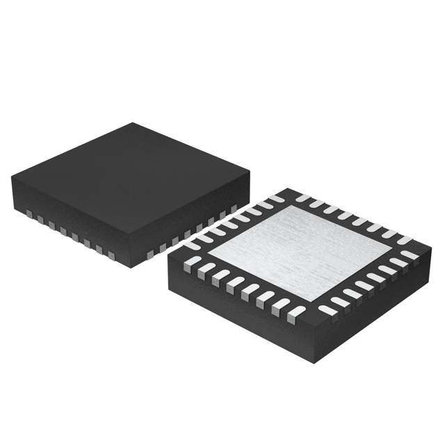
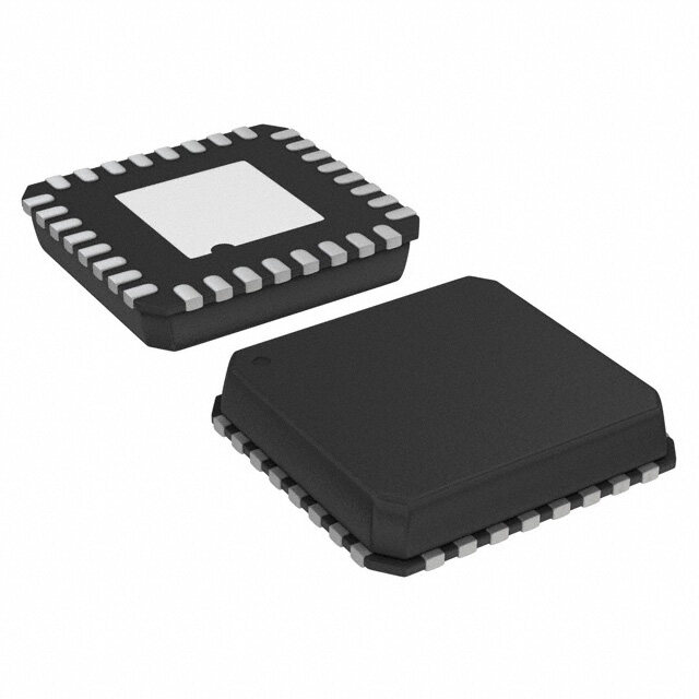
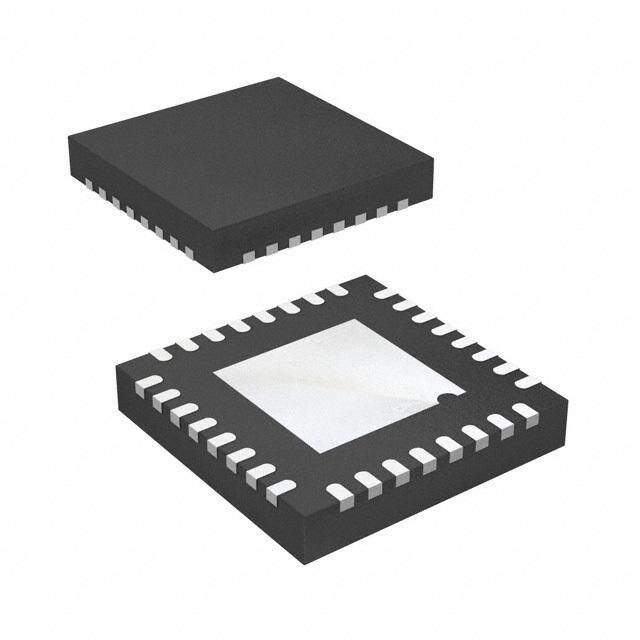
| 描述 | IC RF TXRX FOR NARROWBAND 32QFN |
| 产品分类 | RF 收发器 |
| 品牌 | Texas Instruments |
| 数据手册 | http://www.ti.com/lit/pdf/swrz039点击此处下载产品Datasheet |
| 产品图片 |
|
| 产品型号 | CC1125RHBR |
| PCN设计/规格 | |
| rohs | 无铅 / 符合限制有害物质指令(RoHS)规范要求 |
| 产品系列 | - |
| 其它名称 | 296-35669-2 |
| 制造商产品页 | http://www.ti.com/general/docs/suppproductinfo.tsp?distId=10&orderablePartNumber=CC1125RHBR |
| 功率-输出 | 16dBm |
| 包装 | 带卷 (TR) |
| 天线连接器 | PCB,表面贴装 |
| 存储容量 | - |
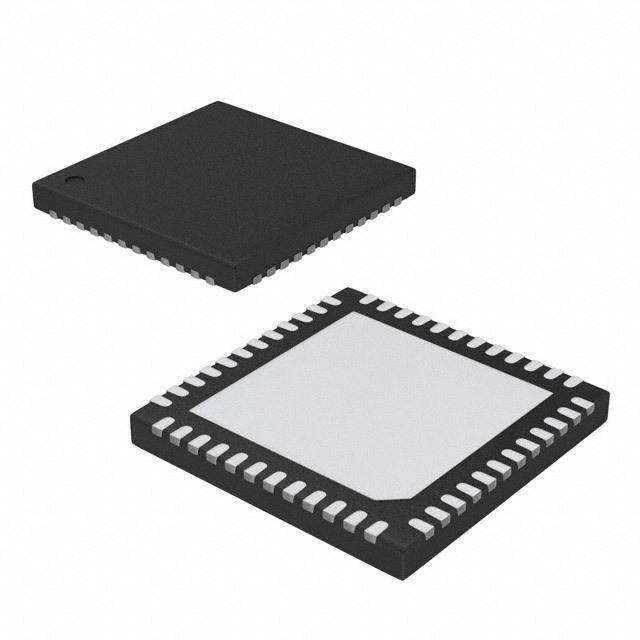
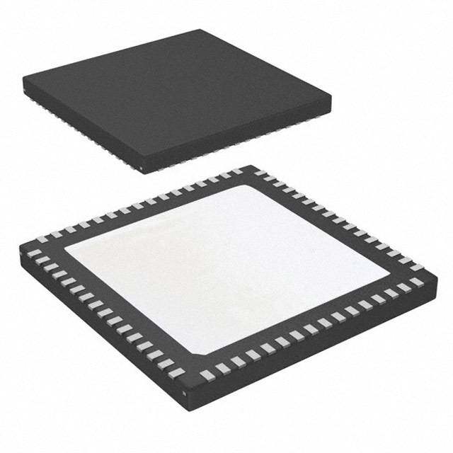
| 封装/外壳 | 32-VFQFN 裸露焊盘 |
| 工作温度 | -40°C ~ 85°C |
| 应用 | 通用 |
| 数据接口 | PCB,表面贴装 |
| 数据速率(最大值) | 200kbps |
| 标准包装 | 3,000 |
| 灵敏度 | -129dBm |
| 电压-电源 | 2 V ~ 3.6 V |
| 电流-传输 | 56mA |
| 电流-接收 | 27mA |
| 调制或协议 | 802.15.4 |
| 频率 | 164MHz ~ 192MHz,274MHz ~ 320MHz,410MHz ~ 480MHz,820MHz ~ 960MHz |


- 商务部:美国ITC正式对集成电路等产品启动337调查
- 曝三星4nm工艺存在良率问题 高通将骁龙8 Gen1或转产台积电
- 太阳诱电将投资9.5亿元在常州建新厂生产MLCC 预计2023年完工
- 英特尔发布欧洲新工厂建设计划 深化IDM 2.0 战略
- 台积电先进制程称霸业界 有大客户加持明年业绩稳了
- 达到5530亿美元!SIA预计今年全球半导体销售额将创下新高
- 英特尔拟将自动驾驶子公司Mobileye上市 估值或超500亿美元
- 三星加码芯片和SET,合并消费电子和移动部门,撤换高东真等 CEO
- 三星电子宣布重大人事变动 还合并消费电子和移动部门
- 海关总署:前11个月进口集成电路产品价值2.52万亿元 增长14.8%


PDF Datasheet 数据手册内容提取
Product Sample & Technical Tools & Support & Folder Buy Documents Software Community CC1125 SWRS120E–JUNE2011–REVISEDOCTOBER2014 CC1125 Ultra-High Performance RF Narrowband Transceiver 1 Device Overview 1.1 Features 1 • High-Performance,Single-ChipTransceiver • ProgrammableOutputPowerupto+16dBmWith – AdjacentChannelSelectivity:67dBat 0.4-dBStepSize 6.25-kHzOffset • AutomaticOutputPowerRamping – BlockingPerformance:104dBat10MHz • ConfigurableDataRates:0to200kbps – ExcellentReceiverSensitivity • SupportedModulationFormats:2-FSK, • –129dBmat300bps 2-GFSK,4-FSK,4-GFSK,MSK,OOK • –123dBmat1.2kbps • WaveMatch:AdvancedDigitalSignalProcessing forImprovedSyncDetectPerformance • –110dBmat50kbps • RoHS-Compliant5-mmx5-mmNo-LeadQFN – VeryLowPhaseNoise: –115dBc/Hzat 32-PinPackage(RHB) 10-kHzOffset • Regulations –SuitableforSystemsTargeting • SuitableforSystemsTargetingETSI ComplianceWith Category1 – Europe:ETSIEN300220Category1,ETSIEN • Separate128-ByteRXandTXFIFOs 54-25,ETSIEN300113,andEN301166 • SupportforSeamlessIntegrationWiththeCC1190 – US:FCCCFR47Part15,24,90,101 DeviceforIncreasedRangeGivingupto3-dB ImprovementinSensitivityandupto+27-dBm – Japan:ARIBRCRSTD-T30,T-67,T-108 OutputPower • PeripheralsandSupportFunctions • HighSpectralEfficiency(9.6kbpsin12.5-kHz – eWORFunctionalityforAutomaticLow-Power ChannelinComplianceWithFCCNarrowbanding ReceivePolling Mandate) – IncludesFunctionsforAntennaDiversity • PowerSupply Support – WideSupplyVoltageRange(2.0Vto3.6V) – SupportforRetransmissions – LowCurrentConsumption: – SupportforAuto-AcknowledgeofReceived • RX:2mAinRXSniffMode Packets • RX:17mAPeakCurrentinLow-Power – TCXOSupportandControl,alsoinPower Mode Modes • RX:26mAPeakCurrentinHigh- – AutomaticClearChannelAssessment(CCA)for PerformanceMode Listen-Before-Talk(LBT)Systems • TX:47mAat+14dBm – Built-inCodingGainSupportforIncreased RangeandRobustness – PowerDown:0.12 μA(0.5 μAWithEnhanced Wake-On-Radio(eWOR)TimerRunning) – DigitalRSSIMeasurement – TemperatureSensor 1.2 Applications • SocialAlarms • IEEE802.15.4gSystems • NarrowbandUltra-Low-PowerWirelessSystems • HomeandBuildingAutomation WithChannelSpacingDownto4kHz • WirelessAlarmandSecuritySystems • 169-,315-,433-,868-,915-,920-,950-MHz • IndustrialMonitoringandControl ISM/SRDBandSystems • WirelessHealthcareApplications • WirelessMeteringandWirelessSmartGrid(AMR • WirelessSensorNetworksandActiveRFID andAMI) • PrivateMobileRadios 1 AnIMPORTANTNOTICEattheendofthisdatasheetaddressesavailability,warranty,changes,useinsafety-criticalapplications, intellectualpropertymattersandotherimportantdisclaimers.PRODUCTIONDATA.
CC1125 SWRS120E–JUNE2011–REVISEDOCTOBER2014 www.ti.com 1.3 Description The CC1125 device is a fully integrated single-chip radio transceiver designed for high performance at very low-power and low-voltage operation in cost-effective wireless systems. All filters are integrated, thus removing the need for costly external SAW and IF filters. The device is mainly intended for the ISM (Industrial, Scientific and Medical) and SRD (Short Range Device) frequency bands at 164–192 MHz, 274–320MHz,410–480MHz,and820–960MHz. The CC1125 device provides extensive hardware support for packet handling, data buffering, burst transmissions, clear channel assessment, link quality indication, and Wake-On-Radio. The main operating parameters of the CC1125 device can be controlled through an SPI interface. In a typical system, the CC1125devicewillbeusedwithamicrocontrollerandonlyafewexternalpassivecomponents. DeviceInformation(1) PARTNUMBER PACKAGE BODYSIZE CC1125RHB VQFN(32) 5.00mmx5.00mm (1) Formoreinformation,seeSection8,MechanicalPackagingandOrderableInformation 1.4 Functional Block Diagram Figure1-1showsthesystemblockdiagramoftheCC1125device. CC112X (optcioloncakl 3in2tpkHutz) autUo-ltcraal ilborwa tpeodw ReCr 3o2skcHillza tor Power on reset 4Rk ObyMte MUalitnra R loawdMMi opAC oRCUwCoenrt r1o6l Ubnit it Saenrdia dl acotSanP finiIg tuerrafaticoen CSn (chip select) SI (serial input) System bus Interrupt and SO (serial output) IO handler SCLK (serial clock) EnWhaankcee Ode nuW lRtOraaRd loiow t ipmoewrer Batettmerpy sseennssoorr / Csotnaftiugsu rraetgioisnte arnsd F2IF5bO6u f bfReyArteM aPnadc FkIeFtO h acnodnlterorl (optional GPIO0-3) RF and DSP frontend Output power ramping and OOK / ASK modulation (optional autodetected external XOSC / TCXO) PA e1f4ficdiBemnc yh iPghA QI FuFllyre inqtueegnracyte Sdy Fnrtahcetsioiznearl-N Modulator sDigantaa li ncthearifna caec cweitshs XOSC XXOOSSCC__QQ12 90dB dynamic LNA_P ifamp range ADC (optional bit clock) HighL lNinAearity Channel filter Cordic Highly dfleemxiboldeu FlaStoKr / OOK (optional low jitter serial LNA_N ifamp 90radnBg dey AnDamCic dparotato ocoultsp)ut for legacy AGC (optional GPIO for Automatic Gain Control, 60dB VGA range antenna diversity) RSSI measurements and carrier sense detection Figure1-1.FunctionalBlockDiagram 2 DeviceOverview Copyright©2011–2014,TexasInstrumentsIncorporated SubmitDocumentationFeedback ProductFolderLinks:CC1125
CC1125 www.ti.com SWRS120E–JUNE2011–REVISEDOCTOBER2014 Table of Contents 1 DeviceOverview......................................... 1 4.15 High-SpeedClockInput(TCXO).................... 19 .............................................. .................................. 1.1 Features 1 4.16 32-kHzClockInput 19 ........................................... ........................... 1.2 Applications 1 4.17 LowSpeedRCOscillator 20 ............................................ ....................................... 1.3 Description 2 4.18 I/OandReset 20 ............................ ............................... 1.4 FunctionalBlockDiagram 2 4.19 TemperatureSensor 20 2 Revision History......................................... 4 4.20 Typical Characteristics.............................. 21 3 TerminalConfigurationandFunctions.............. 5 5 DetailedDescription................................... 24 .......................................... ....................................... 3.1 PinDiagram 5 5.1 BlockDiagram 24 ..................................... .............................. 3.2 PinConfiguration 6 5.2 FrequencySynthesizer 24 4 Specifications ............................................ 7 5.3 Receiver............................................. 25 .......................... .......................................... 4.1 AbsoluteMaximumRatings 7 5.4 Transmitter 25 ..................................... ................... 4.2 Handling Ratings 7 5.5 RadioControlandUserInterface 25 4.3 RecommendedOperatingConditions(General 5.6 4.5EnhancedWake-On-Radio(eWOR)............ 25 ....................................... Characteristics) 7 ........................................... 5.7 SniffMode 26 4.4 ThermalResistanceCharacteristicsforRHB ................................... .............................................. 5.8 AntennaDiversity 26 Package 7 .......................................... .................................... 5.9 WaveMatch 27 4.5 RF Characteristics 8 6 TypicalApplicationCircuit........................... 28 ................................ 4.6 RegulatoryStandards 8 7 DeviceandDocumentationSupport............... 29 ................. 4.7 CurrentConsumption,StaticModes 9 ...................................... .............. 7.1 DeviceSupport 29 4.8 CurrentConsumption,TransmitModes 9 ............................. .............. 7.2 DocumentationSupport 30 4.9 CurrentConsumption,ReceiveModes 10 .............................. ................................. 7.3 CommunityResources 30 4.10 ReceiveParameters 11 .......................................... ................................ 7.4 Trademarks 30 4.11 Transmit Parameters 17 ..................... ..................................... 7.5 ElectrostaticDischargeCaution 30 4.12 PLLParameters 18 ............................................. ................................ 7.6 Glossary 30 4.13 Wake-upandTiming 19 8 MechanicalPackagingandOrderable ....................... 4.14 High-SpeedCrystalOscillator 19 Information.............................................. 31 Copyright©2011–2014,TexasInstrumentsIncorporated TableofContents 3 SubmitDocumentationFeedback ProductFolderLinks:CC1125
CC1125 SWRS120E–JUNE2011–REVISEDOCTOBER2014 www.ti.com 2 Revision History NOTE:Pagenumbersforpreviousrevisionsmaydifferfrompagenumbersinthecurrentversion. This data manual revision history highlights the changes made to the SWRS120D device-specific data manualtomakeitanSWRS120Erevision. ChangesfromRevisionD(June2014)toRevisionE Page • AddedAmbienttothetemperaturerangeconditionandremovedTjfromTemperaturerange ........................... 7 • AddeddatatoTCXOtable......................................................................................................... 19 4 RevisionHistory Copyright©2011–2014,TexasInstrumentsIncorporated SubmitDocumentationFeedback ProductFolderLinks:CC1125
CC1125 www.ti.com SWRS120E–JUNE2011–REVISEDOCTOBER2014 3 Terminal Configuration and Functions 3.1 Pin Diagram Figure3-1showspinnamesandlocationsfortheCC1125device. P P 2 H H C SC SC NTH D_C D_C OS Q2 Q1 XO XO SY PF PF _X C_ C_ L_ D_ D_ L_ D_ T S S P D D P D X O O C V V C V E X X D A A D A 2 1 0 9 8 7 6 5 3 3 3 2 2 2 2 2 VDD_GUARD 1 24 LPF1 RESET_N 2 23 LPF0 GPIO3 3 22 AVDD_SYNTH1 GPIO2 4 21 DCPL_VCO CC1125 DVDD 5 20 LNA_N DCPL 6 19 LNA_P SI 7 GND 18 TRX_SW SCLK 8 GROUND PAD 17 PA 9 10 11 12 13 14 15 16 S G C D A R A N O (GP PIO0 Sn VDD VDD_ BIAS VDD_ .C. IO IF RF 1 ) Figure3-1.Package5-mm ×5-mmQFN Copyright©2011–2014,TexasInstrumentsIncorporated TerminalConfigurationandFunctions 5 SubmitDocumentationFeedback ProductFolderLinks:CC1125
CC1125 SWRS120E–JUNE2011–REVISEDOCTOBER2014 www.ti.com 3.2 Pin Configuration Thefollowingtableliststhepin-outconfigurationfortheCC1125device. PINNO. PINNAME TYPE/ DESCRIPTION DIRECTION 1 VDD_GUARD Power 2.0–3.6VVDD 2 RESET_N Digitalinput Asynchronous,active-lowdigitalreset 3 GPIO3 DigitalI/O General-purposeI/O 4 GPIO2 DigitalI/O General-purposeI/O 5 DVDD Power 2.0–3.6VDDtointernaldigitalregulator 6 DCPL Power Digitalregulatoroutputtoexternaldecouplingcapacitor 7 SI Digitalinput Serialdatain 8 SCLK Digitalinput Serialdataclock 9 SO(GPIO1) DigitalI/O Serialdataout(general-purposeI/O) 10 GPIO0 DigitalI/O General-purposeI/O 11 CSn Digitalinput Active-lowchipselect 12 DVDD Power 2.0–3.6VVDD 13 AVDD_IF Power 2.0–3.6VVDD 14 RBIAS Analog Externalhigh-precisionresistor 15 AVDD_RF Power 2.0–3.6VVDD 16 N.C. Notconnected 17 PA Analog Single-endedTXoutput(requiresDCpathtoVDD) TXandRXswitch.ConnectedinternallytoGNDinTXandfloating(high-impedance) 18 TRX_SW Analog inRX. 19 LNA_P Analog DifferentialRXinput(requiresDCpathtoGND) 20 LNA_N Analog DifferentialRXinput(requiresDCpathtoGND) 21 DCPL_VCO Power PinforexternaldecouplingofVCOsupplyregulator 22 AVDD_SYNTH1 Power 2.0–3.6VVDD 23 LPF0 Analog Externalloopfiltercomponents 24 LPF1 Analog Externalloopfiltercomponents 25 AVDD_PFD_CHP Power 2.0–3.6VVDD 26 DCPL_PFD_CHP Power PinforexternaldecouplingofPFDandCHPregulator 27 AVDD_SYNTH2 Power 2.0–3.6VVDD 28 AVDD_XOSC Power 2.0–3.6VVDD 29 DCPL_XOSC Power PinforexternaldecouplingofXOSCsupplyregulator Crystaloscillatorpin1(mustbegroundedifaTCXOorotherexternalclock 30 XOSC_Q1 Analog connectedtoEXT_XOSCisused) Crystaloscillatorpin2(mustbeleftfloatingifaTCXOorotherexternalclock 31 XOSC_Q2 Analog connectedtoEXT_XOSCisused) Pinforexternalclockinput(mustbegroundedifaregularcrystalconnectedto 32 EXT_XOSC Digitalinput XOSC_Q1andXOSC_Q2isused) – GND Groundpad Thegroundpadmustbeconnectedtoasolidgroundplane. 6 TerminalConfigurationandFunctions Copyright©2011–2014,TexasInstrumentsIncorporated SubmitDocumentationFeedback ProductFolderLinks:CC1125
CC1125 www.ti.com SWRS120E–JUNE2011–REVISEDOCTOBER2014 4 Specifications All measurements performed on CC1120EM_868_915 rev.1.0.1, CC1120EM_955 rev.1.2.1, CC1120EM_420_470 rev.1.0.1 or CC1120EM_169 rev.1.2 (f = 32 MHz), and CC1125EM_868_915 xosc rev.1.1.0, CC1125EM_420_470 rev.1.1.0, CC1125EM_169 rev.1.1.0, CC1125EM-Cat1-868 (f = 40 xosc MHz). 4.1 Absolute Maximum Ratings(1)(2) PARAMETER MIN MAX UNIT CONDITION Supplyvoltage(VDD,AVDD_x) –0.3 3.9 V Allsupplypinsmusthavethesamevoltage Solderreflowtemperature 260 °C AccordingtoIPC/JEDECJ-STD-020 InputRFlevel +10 dBm Voltageonanydigitalpin –0.3 VDD+0.3 V max3.9 Voltageonanalogpins –0.3 2.0 V (includingDCPLpins) (1) Stressesbeyondthoselistedunderabsolutemaximumratingsmaycausepermanentdamagetothedevice.Thesearestressratings only,andfunctionaloperationofthedeviceattheseoranyotherconditionsbeyondthoseindicatedundergeneralcharacteristicsisnot implied.Exposuretoabsolute-maximum-ratedconditionsforextendedperiodsmayaffectdevicereliability. (2) AllvoltagevaluesarewithrespecttoV ,unlessotherwisenoted. SS 4.2 Handling Ratings MIN MAX UNIT T Storagetemperaturerange –40 125 °C stg Electrostatic Humanbodymodel(HBM),perANSI/ESDA/JEDECJS001(1) –2 2 kV VESD discharge(ESD) Chargeddevicemodel(CDM),perJESD22- performance: C101(2) Allpins –500 500 V (1) JEDECdocumentJEP155statesthat500-VHBMallowssafemanufacturingwithastandardESDcontrolprocess. (2) JEDECdocumentJEP157statesthat250-VHBMallowssafemanufacturingwithastandardESDcontrolprocess. 4.3 Recommended Operating Conditions (General Characteristics) PARAMETER MIN TYP MAX UNIT CONDITION Voltagesupplyrange 2.0 3.6 V Allsupplypinsmusthavethesamevoltage Voltageondigitalinputs 0 VDD V Temperaturerange –40 85 °C Ambient 4.4 Thermal Resistance Characteristics for RHB Package °C/W(1) AIRFLOW(m/s)(2) Rθ Junction-to-case(top) 21.1 0.00 JC Rθ Junction-to-board 5.3 0.00 JB Rθ Junction-to-freeair 31.3 0.00 JA Psi Junction-to-packagetop 0.2 0.00 JT Psi Junction-to-board 5.3 0.00 JB Rθ Junction-to-case(bottom) 0.8 0.00 JC (1) ThesevaluesarebasedonaJEDEC-defined2S2Psystem(withtheexceptionoftheThetaJC[RΘ ]value,whichisbasedona JC JEDEC-defined1S0Psystem)andwillchangebasedonenvironmentaswellasapplication.Formoreinformation,seethese EIA/JEDECstandards: • JESD51-2,IntegratedCircuitsThermalTestMethodEnvironmentalConditions-NaturalConvection(StillAir) • JESD51-3,LowEffectiveThermalConductivityTestBoardforLeadedSurfaceMountPackages • JESD51-7,HighEffectiveThermalConductivityTestBoardforLeadedSurfaceMountPackages • JESD51-9,TestBoardsforAreaArraySurfaceMountPackageThermalMeasurements Powerdissipationof40mWandanambienttemperatureof25ºCisassumed. (2) m/s=meterspersecond Copyright©2011–2014,TexasInstrumentsIncorporated Specifications 7 SubmitDocumentationFeedback ProductFolderLinks:CC1125
CC1125 SWRS120E–JUNE2011–REVISEDOCTOBER2014 www.ti.com 4.5 RF Characteristics PARAMETER MIN TYP MAX UNIT CONDITION 820 960 MHz 410 480 MHz (273.3) (320) MHz SeeSWRA398formoreinformation. Frequencybands 164 192 MHz (205) (240) MHz ContactTIformoreinformationaboutthe (136.7) (160) MHz useofthesefrequencybands. 30 Hz In820–950MHzband Frequencyresolution 15 Hz In410–480MHzband 6 Hz In164–192MHzband 0 200 kbps Packetmode Datarate 0 100 kbps Transparentmode Dataratestepsize 1e-4 bps 4.6 Regulatory Standards PERFORMANCEMODE FrequencyBand Suitableforcompliancewith Comments ARIBT-108 ARIBT-96 Performancealsosuitable ETSIEN300220category1 forsystemstargeting ETSIEN54-25 maximumallowedoutput FCCPART101 820–960MHz powerintherespective FCCPART24SUBMASKD bands,usingarange FCCPART15.247 extendersuchasthe FCCPART15.249 CC1190device FCCPART90MASKG FCCPART90MASKJ ARIBT-67 ARIBRCRSTD-30 Performancealsosuitable High-performancemode ETSIEN301166 forsystemstargeting ETSIEN300113 maximumallowedoutput 410–480MHz ETSIEN300220category1 powerintherespective FCCPART90MASKD bands,usingarange FCCPART90MASKE extender FCCPART90MASKG ETSIEN300220category1 Performancealsosuitable ETSIEN301166 forsystemstargeting ETSIEN300113 maximumallowedoutput 164–192MHz FCCPART90MASKC powerintherespective FCCPART90MASKD bands,usingarange FCCPART90MASKE extender ETSIEN300220category2 820–960MHz FCCPART15.247 FCCPART15.249 Low-powermode 410–480MHz ETSIEN300220category2 164–192MHz ETSIEN300220category2 8 Specifications Copyright©2011–2014,TexasInstrumentsIncorporated SubmitDocumentationFeedback ProductFolderLinks:CC1125
CC1125 www.ti.com SWRS120E–JUNE2011–REVISEDOCTOBER2014 4.7 Current Consumption, Static Modes T =25°C,VDD=3.0V,f =32MHzifnothingelsestated. A xosc PARAMETER MIN TYP MAX UNIT CONDITION 0.12 1 µA Powerdownwithretention 0.5 µA Low-powerRCoscillatorrunning XOFFmode 170 µA Crystaloscillator/TCXOdisabled Clockrunning,systemwaitingwithno IDLEmode 1.3 mA radioactivity 4.8 Current Consumption, Transmit Modes 4.8.1 950-MHz Band (High-Performance Mode) T =25°C,VDD=3.0V,f =32MHzifnothingelsestated A xosc PARAMETER MIN TYP MAX UNIT CONDITION TXcurrentconsumption+10dBm 37 mA TXcurrentconsumption0dBm 26 mA 4.8.2 868-, 915-, and 920-MHz Bands (High-Performance Mode) T =25°C,VDD=3.0V,f =40MHzifnothingelsestated A xosc PARAMETER MIN TYP MAX UNIT CONDITION TXcurrentconsumption+14dBm 47 mA TXcurrentconsumption+10dBm 38 mA 4.8.3 434-MHz Band (High-Performance Mode) T =25°C,VDD=3.0V,f =40MHzifnothingelsestated A xosc PARAMETER MIN TYP MAX UNIT CONDITION TXcurrentconsumption+15dBm 51 mA TXcurrentconsumption+14dBm 47 mA TXcurrentconsumption+10dBm 36 mA 4.8.4 169-MHz Band (High Performance Mode) T =25°C,VDD=3.0V,f =40MHzifnothingelsestated A xosc PARAMETER MIN TYP MAX UNIT CONDITION TXcurrentconsumption+15dBm 56 mA TXcurrentconsumption+14dBm 52 mA TXcurrentconsumption+10dBm 40 mA 4.8.5 Low-Power Mode T =25°C,VDD=3.0V,f =869.5MHz,f =32MHzifnothingelsestated A c xosc PARAMETER MIN TYP MAX UNIT CONDITION TXcurrentconsumption+10dBm 32 mA Copyright©2011–2014,TexasInstrumentsIncorporated Specifications 9 SubmitDocumentationFeedback ProductFolderLinks:CC1125
CC1125 SWRS120E–JUNE2011–REVISEDOCTOBER2014 www.ti.com 4.9 Current Consumption, Receive Modes 4.9.1 High-Performance Mode T =25°C,VDD=3.0V,f =869.5MHz,f =32MHzifnothingelsestated A c xosc PARAMETER MIN TYP MAX UNIT CONDITION RXwaitforsync UsingRXsniffmode,wherethereceiver 1.2kbps,4-bytepreamble 2 mA wakesupatregularintervalstolookforan incomingpacket 38.4kbps,4-bytepreamble 13.4 mA RXpeakcurrent,f =40MHz xosc Peakcurrentconsumptionduringpacket 433-,868-,915-,and920-MHzbands 26 mA receptionatthesensitivitythreshold 169-MHzband 27 mA Averagecurrentconsumption 50kbps,5-bytepreamble,40-kHzRC Checkfordatapacketevery1secondusing 15 µA oscillatorusedassleeptimer wakeonradio 4.9.2 Low-Power Mode T =25°C,VDD=3.0V,f =869.5MHz,f =32MHzifnothingelsestated A c xosc PARAMETER MIN TYP MAX UNIT CONDITION RXpeakcurrentlow-powerRXmode Peakcurrentconsumptionduringpacket 17 mA 1.2kbps receptionatthesensitivitylevel 10 Specifications Copyright©2011–2014,TexasInstrumentsIncorporated SubmitDocumentationFeedback ProductFolderLinks:CC1125
CC1125 www.ti.com SWRS120E–JUNE2011–REVISEDOCTOBER2014 4.10 Receive Parameters AllRXmeasurementsmadeattheantennaconnector,toabiterrorrate(BER)limitof1%. 4.10.1 General Receive Parameters (High-Performance Mode) T =25°C,VDD=3.0V,f =869.5MHzifnothingelsestated A c PARAMETER MIN TYP MAX UNIT CONDITION Saturation +10 dBm Digitalchannelfilterprogrammablebandwidth f =32MHz 2.8 200 kHz xosc f =40MHz 3.5 250 kHz xosc IIP3,normalmode –14 dBm Atmaximumgain IIP3,highlinearitymode –8 dBm Using6-dBgainreductioninfrontend Withcarriersensedetectionenabledand ±12 % Datarateoffsettolerance assuming4-bytepreamble ±0.2 % Withcarriersensedetectiondisabled Spuriousemissions Radiatedemissionsmeasuredaccordingto 1–13GHz(VCOleakageat3.5GHz) –56 dBm ETSIEN300220,fc=869.5MHz 30MHzto1GHz <–57 dBm Optimumsourceimpedance 868-,915-,and920-MHzbands 60+j60/30+j30 Ω (Differentialorsingle-endedRX 433-MHzband 100+j60/50+j30 Ω configurations) 169-MHzband 140+j40/70+j20 Ω Copyright©2011–2014,TexasInstrumentsIncorporated Specifications 11 SubmitDocumentationFeedback ProductFolderLinks:CC1125
CC1125 SWRS120E–JUNE2011–REVISEDOCTOBER2014 www.ti.com 4.10.2 RX Performance in 950-MHz Band (High-Performance Mode) T =25°C,VDD=3.0V,f =32MHzifnothingelsestated A xosc PARAMETER MIN TYP MAX UNIT CONDITION –120 dBm 1.2kbps,DEV=4kHzCHF=10kHz(1) Sensitivity 50kbps2GFSK,DEV=25kHz,CHF=100 –107 dBm Note:SensitivitycanbeimprovediftheTXand kHz RXmatchingnetworksareseparated. 200kbps,DEV=83kHz(outersymbols), –100 dBm CHF=200kHz,4GFSK(2) 51 dB ±12.5kHz(adjacentchannel) 52 dB ±25kHz(alternatechannel) BlockingandSelectivity 1.2kbps2-FSK,12.5-kHzchannelseparation, 73 dB ±1MHz 4-kHzdeviation,10-kHzchannelfilter 76 dB ±2MHz 81 dB ±10MHz 43 dB ±200kHz(adjacentchannel) BlockingandSelectivity 51 dB ±400kHz(alternatechannel) 50kbps2-GFSK,200-kHzchannelseparation, 25-kHzdeviation,100-kHzchannelfilter 62 dB ±1MHz (Samemodulationformatas802.15.4g 65 dB ±2MHz MandatoryMode) 71 dB ±10MHz 37 dB ±200kHz(adjacentchannel) 44 dB ±400kHz(alternatechannel) BlockingandSelectivity 200kbps4-GFSK,83-kHzdeviation(outer 55 dB ±1MHz symbols),200-kHzchannelfilter,zeroIF 58 dB ±2MHz 64 dB ±10MHz (1) DEVisshortfordeviation,CHFisshortforchannelfilterbandwidth (2) BT=0.5isusedinallGFSKmeasurements 12 Specifications Copyright©2011–2014,TexasInstrumentsIncorporated SubmitDocumentationFeedback ProductFolderLinks:CC1125
CC1125 www.ti.com SWRS120E–JUNE2011–REVISEDOCTOBER2014 4.10.3 RX Performance in 868-, 915-, and 920-MHz Bands (High-Performance Mode) T =25°C,VDD=3.0V,f =32MHzifnothingelsestatedifnothingelsestated A xosc PARAMETER MIN TYP MAX UNIT CONDITION 300bps,DEV=1kHzCHF=3.8kHz(1), –129 dBm f =40MHz xosc –123 dBm 1.2kbps,DEV=20kHzCHF=50kHz –114 dBm 4.8kbpsOOK Sensitivity –110 dBm 38.4kbps,DEV=20kHzCHF=100kHz –110 dBm 50kbps2GFSK,DEV=25kHz,CHF=100kHz 200kbps,DEV=83kHz(outersymbols), –103 dBm CHF=200kHz,4GFSK 62 dB ±6.25kHz(adjacentchannel) BlockingandSelectivity 63 dB ±12.5kHz(alternatechannel) 0.3-kbps2-FSK,6.25-kHzchannel separation,1-kHzdeviation,3.8-kHz 83 dB ±1MHz channelfilter 87 dB ±2MHz f =40MHzusingTCXO xosc 91 dB ±10MHz 58 dB +12.5kHz(adjacentchannel) BlockingandSelectivity 58 dB ±25kHz(alternatechannel) 1.2-kbps2-FSK,12.5-kHzchannel separation,4-kHzdeviation,10-kHz 78 dB ±1MHz channelfilter 82 dB ±2MHz f =40MHzusingTCXO xosc 86 dB ±10MHz BlockingandSelectivity 58 dB ±25kHz(alternatechannel) 1.2-kbps2-GFSK,25-kHzchannel 77 dB ±1MHz separation,4-kHzdeviation,16-kHz channelfilter 106 dB ±2MHz f =40MHzusingTCXO xosc UsingexternalSAWfilterfor 101 dB ±10MHz compliancewithETSIcategory1 42 dB ±100kHz(adjacentchannel) BlockingandSelectivity 43 dB ±200kHz(alternatechannel) 38.4-kbps2-GFSK,100-kHzchannel 62 dB ±1MHz separation,20-kHzdeviation,100- kHzchannelfilter 66 dB ±2MHz 74 dB ±10MHz 43 dB ±200kHz(adjacentchannel) BlockingandSelectivity 50-kbps2-GFSK,200-kHzchannel 50 dB ±400kHz(alternatechannel) separation,25-kHzdeviation,100- 61 dB ±1MHz kHzchannelfilter (Samemodulationformatas 65 dB ±2MHz 802.15.4gMandatoryMode) 74 dB ±10MHz 36 dB ±200kHz(adjacentchannel) BlockingandSelectivity 44 dB ±400kHz(alternatechannel) 200-kbps4-GFSK,83-kHzdeviation 55 dB ±1MHz (outersymbols),200-kHzchannel filter,zeroIF 59 dB ±2MHz 67 dB ±10MHz Imagerejection 1.2kbps,DEV=4kHzCHF=10kHz(1),imageat (Imagecompensationenabled) 58 dB -125kHz f =40MHzusingTCXO xosc (1) DEVisshortfordeviation,CHFisshortforchannelfilterbandwidth Copyright©2011–2014,TexasInstrumentsIncorporated Specifications 13 SubmitDocumentationFeedback ProductFolderLinks:CC1125
CC1125 SWRS120E–JUNE2011–REVISEDOCTOBER2014 www.ti.com 4.10.4 RX Performance in 434-MHz Band (High-Performance Mode) T =25°C,VDD=3.0V,f =32MHzifnothingelsestatedifnothingelsestated A xosc PARAMETER MIN TYP MAX UNIT CONDITION 300bps,DEV=1kHz,CHF=3.8kHz(1) –129 dBm f =40MHz xosc –123 dBm 1.2kbps,DEV=4kHzCHF=10kHz(1) Sensitivity 50-kbps2-GFSK,DEV=25kHz,CHF=100 –109 dBm kHz(1) –116 dBm 1.2kbps,DEV=20kHzCHF=50kHz(1) 65 dB +6.25kHz(adjacentchannel) BlockingandSelectivity 66 dB +12.5kHz(alternatechannel) 0.3-kbps2-FSK,6.25-kHzchannel separation,1-kHzdeviation,3.8-kHz 86 dB ±1MHz channelfilter 90 dB ±2MHz f =40MHzusingTCXO xosc 95 dB ±10MHz 60 dB +12.5kHz(adjacentchannel) BlockingandSelectivity 61 dB ±25kHz(alternatechannel) 1.2-kbps2-FSK,12.5-kHzchannel separation,4-kHzdeviation,10-kHz 80 dB ±1MHz channelfilter 85 dB ±2MHz f =40MHzusingTCXO xosc 91 dB ±10MHz 47 dB +100kHz(adjacentchannel) BlockingandSelectivity 50 dB ±200kHz(alternatechannel) 38.4-kbps2-GFSK,100-kHzchannel 67 dB ±1MHz separation,20-kHzdeviation,100-kHz channelfilter 71 dB ±2MHz 78 dB ±10MHz (1) DEVisshortfordeviation,CHFisshortforchannelfilterbandwidth 14 Specifications Copyright©2011–2014,TexasInstrumentsIncorporated SubmitDocumentationFeedback ProductFolderLinks:CC1125
CC1125 www.ti.com SWRS120E–JUNE2011–REVISEDOCTOBER2014 4.10.5 RX Performance in 169-MHz Band (High-Performance Mode) T =25°C,VDD=3.0V,f =32MHzifnothingelsestated A xosc PARAMETER MIN TYP MAX UNIT CONDITION 300bps,DEV=1kHz,CHF=3.8kHz(1) –129 dBm Sensitivity fxosc=40MHz –123 dBm 1.2kbps,DEV=4kHzCHF=10kHz(1) 67 dB ±6.25kHz(adjacentchannel) BlockingandSelectivity 67 dB +12.5kHz(alternatechannel) 0.3-kbps2-FSK,6.25-kHzchannel separation,1-kHzdeviation,3.8-kHz 88 dB ±1MHz channelfilter 101 dB –2MHz f =40MHzusingTCXO xosc 104 dB ±10MHz 63 dB ±12.5kHz(adjacentchannel) BlockingandSelectivity 65 dB ±25kHz(alternatechannel) 1.2-kbps2-FSK,12.5-kHzchannel separation,4-kHzdeviation,10-kHz 82 dB ±1MHz channelfilter 86 dB ±2MHz f =40MHzusingTCXO xosc 93 dB –10MHz SpuriousResponseRejection 1.2-kbps2-FSK,12.5-kHzchannel 70 dB separation,4-kHzdeviation,10-kHz channelfilter ImageRejection 1.2kbps,DEV=4kHzCHF=10kHz(1),imageat 66 dB (Imagecompensationenabled) –125kHz (1) DEVisshortfordeviation,CHFisshortforchannelfilterbandwidth Copyright©2011–2014,TexasInstrumentsIncorporated Specifications 15 SubmitDocumentationFeedback ProductFolderLinks:CC1125
CC1125 SWRS120E–JUNE2011–REVISEDOCTOBER2014 www.ti.com 4.10.6 RX Performance in Low-Power Mode T =25°C,VDD=3.0V,f =869.5MHz,f =32MHzifnothingelsestated A c xosc PARAMETER MIN TYP MAX UNIT CONDITION –111 dBm 1.2kbps,DEV=4kHzCHF=10kHz(1) –99 dBm 38.4kbps,DEV=50kHzCHF=100kHz(1) Sensitivity 50-kbps2-GFSK,DEV=25kHz,CHF=100 –99 dBm kHz(1) 46 dB ±12.5kHz(adjacentchannel) BlockingandSelectivity 46 dB ±25kHz(alternatechannel) 1.2-kbps2-FSK,12.5-kHzchannel 73 dB ±1MHz separation,4-kHzdeviation,10-kHzchannel filter 78 dB ±2MHz 79 dB ±10MHz 43 dB ±50kHz(adjacentchannel) 45 dB +100kHz(alternatechannel) BlockingandSelectivity 1.2-kbps2-FSK,50-kHzchannelseparation, 71 dB ±1MHz 20-kHzdeviation,50-kHzchannelfilter 74 dB ±2MHz 75 dB ±10MHz 37 dB +100kHz(adjacentchannel) BlockingandSelectivity 43 dB +200kHz(alternatechannel) 38.4-kbps2-GFSK,100-kHzchannel 58 dB ±1MHz separation,20-kHzdeviation,100-kHz channelfilter 62 dB ±2MHz 64 dB +10MHz 43 dB +200kHz(adjacentchannel) BlockingandSelectivity 50-kbps2-GFSK,200-kHzchannel 52 dB +400kHz(alternatechannel) separation,25-kHzdeviation,100-kHz 60 dB ±1MHz channelfilter (Samemodulationformatas802.15.4g 64 dB ±2MHz MandatoryMode) 65 dB ±10MHz Saturation +10 dBm (1) DEVisshortfordeviation,CHFisshortforchannelfilterbandwidth 16 Specifications Copyright©2011–2014,TexasInstrumentsIncorporated SubmitDocumentationFeedback ProductFolderLinks:CC1125
CC1125 www.ti.com SWRS120E–JUNE2011–REVISEDOCTOBER2014 4.11 Transmit Parameters T =25°C,VDD=3.0V,f =869.5MHz,f =32MHzifnothingelsestated A c xosc PARAMETER MIN TYP MAX UNIT CONDITION +12 dBm At950MHz +14 dBm At915-and920-MHz +15 dBm At915-and920-MHzwithVDD=3.6V +15 dBm At868MHz Maxoutputpower +16 dBm At868MHzwithVDD=3.6V +15 dBm At433MHz +16 dBm At433MHzwithVDD=3.6V +15 dBm At169MHz +16 dBm At169MHzwithVDD=3.6V –11 dBm Withinfinestepsizerange Minoutputpower –40 dBm Withincoarsestepsizerange Outputpowerstepsize 0.4 dB Withinfinestepsizerange 4-GFSK9.6kbpsin12.5-kHzchannel, –75 dBc measuredin100-Hzbandwidthat434MHz (FCCPart90MaskDcompliant) 4-GFSK9.6kbpsin12.5-kHzchannel, Adjacentchannelpower –58 dBc measuredin8.75-kHzbandwidth(ETSI300220 compliant) 2-GFSK2.4kbpsin12.5-kHzchannel,1.2-kHz –61 dBc deviation Spuriousemissions <–60 dBm (notincludingharmonics) Harmonics SecondHarm,169MHz –39 dBm ThirdHarm,169MHz –58 dBm SecondHarm,433MHz –56 dBm Transmissionat+14dBm(ormaximumallowed ThirdHarm,433MHz –51 dBm inapplicablebandwherethisislessthan+14 SecondHarm,450MHz –60 dBm dBm)usingTIreferencedesign. EmissionsmeasuredaccordingtoARIBT-96in ThirdHarm,450MHz –45 dBm 950-MHzband,ETSIEN300-220in169-,433-, SecondHarm,868MHz –40 dBm and868-MHzbandsandFCCpart15.247in 450-and915-MHzband. ThirdHarm,868MHz –42 dBm Fourthharmonicin915-MHzbandwillrequire SecondHarm,915MHz 56 dBuV/m extrafilteringtomeetFCCrequirementsif transmittingforlongintervals(>50-msperiods). ThirdHarm,915MHz 52 dBuV/m FourthHarm,915MHz 60 dBuV/m SecondHarm,950MHz –58 dBm ThirdHarm,950MHz –42 dBm Optimumload Impedance868-,915-,and920-MHzbands 35+j35 Ω 433-MHzband 55+j25 Ω 169-MHzband 80+j0 Ω Copyright©2011–2014,TexasInstrumentsIncorporated Specifications 17 SubmitDocumentationFeedback ProductFolderLinks:CC1125
CC1125 SWRS120E–JUNE2011–REVISEDOCTOBER2014 www.ti.com 4.12 PLL Parameters 4.12.1 High-Performance Mode T =25°C,VDD=3.0V,f =869.5MHz,f =40MHzusingTCXOifnothingelsestated A c xosc PARAMETER MIN TYP MAX UNIT CONDITION –100 dBc/Hz ±10kHzoffset Phasenoisein950-MHzband –103 dBc/Hz ±100kHzoffset f =32MHz xosc –123 dBc/Hz ±1MHzoffset –101 dBc/Hz ±10kHzoffset Phasenoisein868-,915-,920-MHzbands –102 dBc/Hz ±100kHzoffset –124 dBc/Hz ±1MHzoffset –107 dBc/Hz ±10kHzoffset Phasenoisein433-MHzband –110 dBc/Hz ±100kHzoffset –130 dBc/Hz ±1MHzoffset –115 dBc/Hz ±10kHzoffset Phasenoisein169-MHzband –115 dBc/Hz ±100kHzoffset –135 dBc/Hz ±1MHzoffset 4.12.2 Low-Power Mode T =25°C,VDD=3.0V,f =869.5MHz,f =32MHzifnothingelsestated A c xosc PARAMETER MIN TYP MAX UNIT CONDITION –90 dBc/Hz ±10kHzoffset Phasenoisein950-MHzband –92 dBc/Hz ±100kHzoffset –124 dBc/Hz ±1MHzoffset –95 dBc/Hz ±10kHzoffset Phasenoisein868-,915-,and920-MHz –95 dBc/Hz ±100kHzoffset bands –124 dBc/Hz ±1MHzoffset –98 dBc/Hz ±10kHzoffset Phasenoisein433-MHzband –102 dBc/Hz ±100kHzoffset –129 dBc/Hz ±1MHzoffset –106 dBc/Hz ±10kHzoffset Phasenoisein169-MHzband –110 dBc/Hz ±100kHzoffset –136 dBc/Hz ±1MHzoffset 18 Specifications Copyright©2011–2014,TexasInstrumentsIncorporated SubmitDocumentationFeedback ProductFolderLinks:CC1125
CC1125 www.ti.com SWRS120E–JUNE2011–REVISEDOCTOBER2014 4.13 Wake-up and Timing T =25°C,VDD=3.0V,f =869.5MHz,f =32MHzifnothingelsestated A c xosc PARAMETER MIN TYP MAX UNIT CONDITION PowerdowntoIDLE 0.4 ms Dependsoncrystal 166 µs Calibrationdisabled IDLEtoRX/TX 461 µs Calibrationenabled RX/TXturnaround 50 µs 296 µs CalibratewhenleavingRX/TXenabled RX/TXtoIDLEtime 0 µs CalibratewhenleavingRX/TXdisabled Frequencysynthesizercalibration 391 µs WhenusingSCALstrobe RequiredforRFfront-endgainsettlingonly. Minimumrequirednumberofpreamblebytes 0.5 bytes Digitaldemodulationdoesnotrequirepreamble forsettling. TimefromstartRXuntilvalidRSSI, 4.6 ms 12.5-kHzchannels includinggainsettling(functionofchannel bandwidth.Programmablefortrade-off 0.3 ms 200-kHzchannels betweenspeedandaccuracy) 4.14 High-Speed Crystal Oscillator T =25°C,VDD=3.0Vifnothingelsestated A PARAMETER MIN TYP MAX UNIT CONDITION Itisexpectedthattherewillbedegraded sensitivityatmultiplesofXOSC/2inRX,andan increaseinspuriousemissionswhentheRF channelisclosetomultiplesofXOSCinTX.We Crystalfrequency 32 44 MHz recommendthattheRFchanneliskept RX_BW/2awayfromXOSC/2inRX,andthat thelevelofspuriousemissionsbeevaluatedif theRFchanneliscloserthan1MHztomultiples ofXOSCinTX. Loadcapacitance(C ) 10 pF L ESR <50 Ω Start-uptime 0.4 ms Dependsoncrystal 4.15 High-Speed Clock Input (TCXO) T =25°C,VDD=3.0Vifnothingelsestated A PARAMETER MIN TYP MAX UNIT CONDITION Clockfrequency 32 44 MHz TCXOwithCMOSoutput TCXOwithCMOSoutputdirectly coupledtopinEXT_OSC Highinputvoltage 1.4 VDD V Lowinputvoltage 0 0.6 V Rise/Falltime 2 ns Clippedsineoutput TCXOclippedsineoutputconnected topinEXT_OSCthroughseries Clockinputamplitude(peak-to-peak) 0.8 1.5 V capacitor 4.16 32-kHz Clock Input T =25°C,VDD=3.0Vifnothingelsestated A PARAMETER MIN TYP MAX UNIT CONDITION Clockfrequency 32 kHz 32-kHzclockinputpininputhighvoltage 0.8×VDD V 32-kHzclockinputpininputlowvoltage 0.2×VDD V Copyright©2011–2014,TexasInstrumentsIncorporated Specifications 19 SubmitDocumentationFeedback ProductFolderLinks:CC1125
CC1125 SWRS120E–JUNE2011–REVISEDOCTOBER2014 www.ti.com 4.17 Low Speed RC Oscillator T =25°C,VDD=3.0Vifnothingelsestated A PARAMETER MIN TYP MAX UNIT CONDITION Aftercalibration(calibratedagainstthehigh- Frequency 32/40 kHz speedXOSC) Relativetofrequencyreference(forexample, Frequencyaccuracyaftercalibration ±0.1 % 32-MHzcrystalorTCXO) Initialcalibrationtime 1.6 ms 4.18 I/O and Reset T =25°C,VDD=3.0Vifnothingelsestated A PARAMETER MIN TYP MAX UNIT CONDITION Logicinputhighvoltage 0.8×VDD V Logicinputlowvoltage 0.2×VDD V Logicoutputhighvoltage 0.8×VDD V At4-mAoutputloadorless Logicoutputlowvoltage 0.2×VDD V Power-onresetthreshold 1.3 V VoltageonDVDDpin 4.19 Temperature Sensor T =25°C,VDD=3.0Vifnothingelsestated A PARAMETER MIN TYP MAX UNIT CONDITION Temperaturesensorrange –40 85 °C Changeinsensoroutputvoltageversus Temperaturecoefficient 2.66 mV/°C changeintemperature TypicalsensoroutputvoltageatT =25°C, Typicaloutputvoltage 794 mV A VDD=3.0V Changeinsensoroutputvoltageversus VDDcoefficient 1.17 mV/V changeinVDD The CC1125 device can be configured to provide a voltage proportional to temperature on GPIO1. The temperature can be estimated by measuring this voltage (see Section 4.19, Temperature Sensor). For more information,seethetemperaturesensordesignnote(SWRA415). 20 Specifications Copyright©2011–2014,TexasInstrumentsIncorporated SubmitDocumentationFeedback ProductFolderLinks:CC1125
CC1125 www.ti.com SWRS120E–JUNE2011–REVISEDOCTOBER2014 4.20 Typical Characteristics T =25°C,VDD=3.0V,f =869.5MHzifnothingelsestated. A c All measurements performed on CC1120EM_868_915 rev.1.0.1, CC1120EM_955 rev.1.2.1, CC1120EM_420_470 rev.1.0.1 or CC1120EM_169 rev.1.2 (f = 32 MHz), and CC1125EM_868_915 rev.1.1.0, CC1125EM_420_470 rev.1.1.0, xosc CC1125EM_169rev.1.1.0,CC1125EM-Cat1-868(f =40MHz). xosc Figure4-16wasmeasuredatthe50-Ωantennaconnector. -120 -120 -121 m) m) -121 B B d -122 d vity ( vity ( -122 siti -123 siti n n Se Se -123 -124 -125 -124 -40 0 40 80 2 2.5 3 3.5 Temperature(ºC) SupplyVoltage(V) 1.2kbps,4-kHzDeviation,10-kHzChannelFilterBandwidth 1.2kbps,4-kHzDeviation,10-kHzChannelFilterBandwidth Figure4-1.SensitivityvsTemperature Figure4-2.SensitivityvsVoltage -114 23.2 -116 22.8 m) -118 A) B m 22.4 d -120 ( sitivity ( --112242 Current 22 n 21.6 Se -126 RX 21.2 -128 -130 20.8 3 5 7 9 11 13 15 17 -130 -80 -30 20 SyncWordDetectThreshold InputLevel(dBm) 1.2kbps,4-kHzDeviation,10-kHzChannelFilterBandwidth 1.2kbps,4-kHzdeviation,10-kHzChannelFilterBandwidth Figure4-3.SyncWordSensitivityvsSyncWordDetectThreshold Figure4-4.RXCurrentvsInputLevel 90 90 80 80 70 70 dB) 60 dB) 60 y ( 50 y ( 50 vit vit cti 40 cti 40 ele 30 ele 30 S S 20 20 10 10 0 0 860 862 864 866 868 870 872 874 876 878 868.6 868.8 869 869.2 869.4 869.6 869.8 870 Frequency(MHz) Frequency(MHz) 1.2kbps,4-kHzdeviation,16-kHzChannelFilterBandwidth,Wanted 1.2kbps,4-kHzdeviation,16-kHzChannelFilterBandwidth,Wanted Channelat869.3MHz(–104dBm) Channelat869.3MHz(–104dBm) Figure4-5.SelectivityvsOffsetFrequency(25-kHzChannel Figure4-6.SelectivityvsOffsetFrequency(25-kHzChannel Spacing) Spacing) Copyright©2011–2014,TexasInstrumentsIncorporated Specifications 21 SubmitDocumentationFeedback ProductFolderLinks:CC1125
CC1125 SWRS120E–JUNE2011–REVISEDOCTOBER2014 www.ti.com Typical Characteristics (continued) 100 70 80 60 60 B) 50 d RSSI 2400 ctivity ( 3400 iiqqiiccednisaabblleedd e 0 Sel 20 -20 10 -40 0 -150 -100 -50 0 869.05 869.1 869.15 869.2 869.25 869.3 869.35 InputLevel(dBm) Frequency(MHz) Figure4-7.RSSIvsInputLevel Figure4-8.AutomaticImageCancellation 18 20 m) 16 m) 10 ower(dB 1124 wer (dB -100 P Po -20 put 10 ut Out 8 Outp -30 -40 6 -50 2 2.5 3 3.5 SupplyVoltage(V) 7F 7B 77 73 6F 6B 67 63 5F 5B 57 53 4F 4B 47 43 PApower setting Figure4-9.OutputPowervsVoltage MaxSetting,170MHz Figure4-10.OutputPowerat868MHz vsPAPowerSetting 60 17 50 m) A) B 16.5 m 40 d nt( er( e 30 w 16 urr Po C X 20 ut T utp 15.5 10 O 0 15 7F 7B 77 73 6F 6B 67 63 5F 5B 57 53 4F 4B 47 43 -40 0 40 80 PApower setting Temperature(ºC) Figure4-11.TXCurrentat868MHz Figure4-12.OutputPowervsTemperature vsPAPowerSetting MaxSetting,170MHz,3.6V 22 Specifications Copyright©2011–2014,TexasInstrumentsIncorporated SubmitDocumentationFeedback ProductFolderLinks:CC1125
CC1125 www.ti.com SWRS120E–JUNE2011–REVISEDOCTOBER2014 Typical Characteristics (continued) 200kbps,DEV=83kHz(OuterSymbols),4GFSK 1.2kbps2-FSK,DEV=4kHz Figure4-13.EyeDiagram Figure4-14.EyeDiagram 9.6kbpsin12.5kHzChannel Figure4-15. FCCPart90MaskD Figure4-16.OutputPowervsLoadImpedance(+14-dBmSetting) 3.1 1400 (V) 2.9 mV) 1200 e ( g e ghVolta 22..57 wVoltag 1800000 Hi 2.3 Lo 600 put 2.1 put ut ut 400 O 1.9 O O O 200 PI 1.7 PI G G 1.5 0 0 5 10 15 20 25 30 35 0 5 10 15 20 25 30 35 Current(mA) Current(mA) Figure4-18.GPIOOutputLowVoltagevsCurrentBeingSinked Figure4-17.GPIOOutputHighVoltagevsCurrentBeingSourced Copyright©2011–2014,TexasInstrumentsIncorporated Specifications 23 SubmitDocumentationFeedback ProductFolderLinks:CC1125
CC1125 SWRS120E–JUNE2011–REVISEDOCTOBER2014 www.ti.com 5 Detailed Description 5.1 Block Diagram Figure5-1showsthesystemblockdiagramoftheCC1125device. CC112X (optcioloncakl 3in2tpkHutz) autUo-ltcraal ilborwa tpeodw ReCr 3o2skcHillza tor Power on reset 4Rk ObyMte MUalitnra R loawdMMi opAC oRCUwCoenrt r1o6l Ubnit it Saenrdia dl acotSanP finiIg tuerrafaticoen CSn (chip select) SI (serial input) System bus Interrupt and SO (serial output) IO handler SCLK (serial clock) EnWhaankcee Ode nuW lRtOraaRd loiow t ipmoewrer Batettmerpy sseennssoorr / Csotnaftiugsu rraetgioisnte arnsd F2IF5bO6u f bfReyArteM aPnadc FkIeFtO h acnodnlterorl (optional GPIO0-3) RF and DSP frontend Output power ramping and OOK / ASK modulation (optional autodetected external XOSC / TCXO) PA e1f4ficdiBemnc yh iPghA QI FuFllyre inqtueegnracyte Sdy Fnrtahcetsioiznearl-N Modulator sDigantaa li ncthearifna caec cweitshs XOSC XXOOSSCC__QQ12 90dB dynamic LNA_P ifamp range ADC (optional bit clock) HighL lNinAearity Channel filter Cordic Highly dfleemxiboldeu FlaStoKr / OOK (optional low jitter serial LNA_N ifamp 90radnBg dey AnDamCic dparotato ocoultsp)ut for legacy AGC (optional GPIO for Automatic Gain Control, 60dB VGA range antenna diversity) RSSI measurements and carrier sense detection Figure5-1.SystemBlockDiagram 5.2 Frequency Synthesizer At the center of the CC1125 device there is a fully integrated, fractional-N, ultra-high-performance frequency synthesizer. The frequency synthesizer is designed for excellent phase noise performance, providing very high selectivity and blocking performance. The system is designed to comply with the most stringentregulatoryspectralmasksatmaximumtransmitpower. Either a crystal can be connected to XOSC_Q1 and XOSC_Q2, or a TCXO can be connected to the EXT_XOSC input. The oscillator generates the reference frequency for the synthesizer, as well as clocks for the analog-to-digital converter (ADC) and the digital part. To reduce system cost, CC1125 device has high-accuracy frequency estimation and compensation registers to measure and compensate for crystal inaccuracies. This compensation enables the use of lower cost crystals. If a TCXO is used, the CC1125 device automatically turns on and off the TCXO when needed to support low-power modes and Wake-On- Radiooperation. 24 DetailedDescription Copyright©2011–2014,TexasInstrumentsIncorporated SubmitDocumentationFeedback ProductFolderLinks:CC1125
CC1125 www.ti.com SWRS120E–JUNE2011–REVISEDOCTOBER2014 5.3 Receiver The CC1125 device features a highly flexible receiver. The received RF signal is amplified by the low- noise amplifier (LNA) and is down-converted in quadrature (I/Q) to the intermediate frequency (IF). At IF, theI/Qsignalsaredigitizedbythehighdynamic-rangeADCs. An advanced automatic gain control (AGC) unit adjusts the front-end gain, and enables the CC1125 device to receive strong and weak signals, even in the presence of strong interferers. High-attenuation channels and data filtering enable reception with strong neighbor channel interferers. The I/Q signal is convertedtoaphaseandmagnitudesignaltosupporttheFSKandOOKmodulationschemes. NOTE A unique I/Q compensation algorithm removes any problem of I/Q mismatch, thus avoiding time-consumingandcostlyI/Qimagecalibrationsteps. 5.4 Transmitter The CC1125 transmitter is based on direct synthesis of the RF frequency (in-loop modulation). To use the spectrum effectively, the CC1125 device has extensive data filtering and shaping in TX mode to support high throughput data communication in narrowband channels. The modulator also controls power ramping toremoveissuessuchasspectralsplatteringwhendrivingexternalhigh-powerRFamplifiers. 5.5 Radio Control and User Interface The CC1125 digital control system is built around the main radio control (MARC), which is implemented using an internal high-performance, 16-bit ultra-low-power processor. MARC handles power modes, radio sequencing,andprotocoltiming. A 4-wire SPI serial interface is used for configuration and data buffer access. The digital baseband includes support for channel configuration, packet handling, and data buffering. The host MCU can stay in power-down mode until a valid RF packet is received. This greatly reduces power consumption. When the hostMCUreceivesavalidRFpacket,itburst-readsthedata.Thisreducestherequiredcomputingpower. The CC1125 radio control and user interface are based on the widely used CC1101 transceiver. This relationship enables an easy transition between the two platforms. The command strobes and the main radiostatesarethesameforthetwoplatforms. Forlegacyformats,theCC1125devicealsosupportstwoserialmodes. • Synchronous serial mode: The CC1125 device performs bit synchronization and provides the MCU withabitclockwithassociateddata. • Transparent mode: The CC1125 device outputs the digital baseband signal using a digital interpolation filtertoeliminatejitterintroducedbydigitalfilteringanddemodulation. 5.6 4.5 Enhanced Wake-On-Radio (eWOR) eWOR, using a flexible integrated sleep timer, enables automatic receiver polling with no intervention from the MCU. When the CC1125 device enters RX mode, it listens and then returns to sleep if a valid RF packet is not received. The sleep interval and duty cycle can be configured to make a trade-off between network latency and power consumption. Incoming messages are time-stamped to simplify timer re- synchronization. The eWOR timer runs off an ultra-low-power 32-kHz RC oscillator. To improve timing accuracy, the RC oscillatorcanbeautomaticallycalibratedtotheRFcrystalinconfigurableintervals. Copyright©2011–2014,TexasInstrumentsIncorporated DetailedDescription 25 SubmitDocumentationFeedback ProductFolderLinks:CC1125
CC1125 SWRS120E–JUNE2011–REVISEDOCTOBER2014 www.ti.com 5.7 Sniff Mode The CC1125 device supports quick start up times, and requires few preamble bits. Sniff mode uses these conditionstodramaticallyreducethecurrentconsumptionwhilethereceiveriswaitingfordata. Because the CC1125 device can wake up and settle much faster than the duration of most preambles, it is not required to be in RX mode continuously while waiting for a packet to arrive. Instead, the enhanced Wake-On-Radio feature can be used to put the device into sleep mode periodically. By setting an appropriate sleep time, the CC1125 device can wake up and receive the packet when it arrives with no performance loss. This sequence removes the need for accurate timing synchronization between transmitter and receiver, and lets the user trade off current consumption between the transmitter and receiver. Formoreinformation,seethesniffmodedesignnote(SWRA428). 5.8 Antenna Diversity Antenna diversity can increase performance in a multipath environment. An external antenna switch is required. The CC1201 device uses one of the GPIO pins to automatically control the switch. This device alsosupportsdifferentialoutputcontrolsignalstypicallyusedinRFswitches. If antenna diversity is enabled, the GPIO alternates between high and low states until a valid RF input signal is detected. An optional acknowledge packet can be transmitted without changing the state of the GPIO. An incoming RF signal can be validated by received signal strength or by using the automatic preamble detector. Using the automatic preamble detector ensures a more robust system and avoids the need to setadefinedsignalstrengththreshold(suchathresholdsetsthesensitivitylimitofthesystem). 26 DetailedDescription Copyright©2011–2014,TexasInstrumentsIncorporated SubmitDocumentationFeedback ProductFolderLinks:CC1125
CC1125 www.ti.com SWRS120E–JUNE2011–REVISEDOCTOBER2014 5.9 WaveMatch Advanced capture logic locks onto the synchronization word and does not require preamble settling bytes. Therefore,receiversettlingtimeisreducedtothesettlingtimeoftheAGC,typically4bits. The WaveMatch feature also greatly reduces false sync triggering on noise, further reducing the power consumption and improving sensitivity and reliability. The same logic can also be used as a high- performancepreambledetectortoreliablydetectavalidpreambleinthechannel. SeeSWRC046formoreinformation. Figure5-2.ReceiverConfiguratorin SmartRF™Studio Copyright©2011–2014,TexasInstrumentsIncorporated DetailedDescription 27 SubmitDocumentationFeedback ProductFolderLinks:CC1125
CC1125 SWRS120E–JUNE2011–REVISEDOCTOBER2014 www.ti.com 6 Typical Application Circuit NOTE Thissectionisintendedonlyasanintroduction. Very few external components are required for the operation of the CC1125 device. Figure 6-1 shows a typical application circuit. The board layout will greatly influence the RF performance of the CC1125 device.Figure6-1doesnotshowdecouplingcapacitorsforpowerpins. Optional Voltage Regulator for supply noise isolation Optional ext_vdd in out vdd 40 MHz TPS799xx XOSC/ crystal TCXO d d d d d d v v v 2 1 0 9 8 7 6 5 3 3 3 2 2 2 2 2 (optional control pin SC Q2 Q1 SC SC H2 HP HP from CC1125) vdd 1 VDD_GUARDEXT_XO XOSC_ XOSC_ DCPL_XO AVDD_XO AVDD_SYNT DCPL_PFD_C AVDD_PFD_C LPF1 24 2 23 RESET_N LPF0 3 22 GPIO3 AVDD_SYNTH1 vdd 4 21 GPIO2 DCPL_VCO CC1125 5 20 vdd DVDD LNA_N 6 19 DCPL LNA_P 7 18 SI TRX_SW 8 17 SCLK PA SO (GPIO1) GPIO0 CSn DVDD AVDD_IF RBIAS AVDD_RF N.C. 9 10 11 12 13 14 15 16 dd v d d d d d d v v v MCU connection SPI interface and optional gpio pins Figure6-1.TypicalApplicationCircuit For more information, see the reference designs available for the CC1125 device in Section 7.2, DocumentationSupport. 28 TypicalApplicationCircuit Copyright©2011–2014,TexasInstrumentsIncorporated SubmitDocumentationFeedback ProductFolderLinks:CC1125
CC1125 www.ti.com SWRS120E–JUNE2011–REVISEDOCTOBER2014 7 Device and Documentation Support 7.1 Device Support 7.1.1 Development Support 7.1.1.1 ConfigurationSoftware The CC1125 device can be configured using the SmartRF Studio software (SWRC046). The SmartRF Studio software is highly recommended for obtaining optimum register settings, and for evaluating performanceandfunctionality. 7.1.2 Device and Development-Support Tool Nomenclature To designate the stages in the product development cycle, TI assigns prefixes to the part numbers of all microprocessors (MPUs) and support tools. Each device has one of three prefixes: X, P, or null (no prefix) (for example, CC1125). Texas Instruments recommends two of three possible prefix designators for its support tools: TMDX and TMDS. These prefixes represent evolutionary stages of product development fromengineeringprototypes(TMDX)throughfullyqualifiedproductiondevicesandtools(TMDS). Devicedevelopmentevolutionaryflow: X Experimental device that is not necessarily representative of the final device's electrical specificationsandmaynotuseproductionassemblyflow. P Prototype device that is not necessarily the final silicon die and may not necessarily meet finalelectricalspecifications. null Productionversionofthesilicondiethatisfullyqualified. Supporttooldevelopmentevolutionaryflow: TMDX Development-support product that has not yet completed Texas Instruments internal qualificationtesting. TMDS Fullyqualifieddevelopment-supportproduct. XandPdevicesandTMDXdevelopment-supporttoolsareshippedagainstthefollowingdisclaimer: "Developmentalproductisintendedforinternalevaluationpurposes." Production devices and TMDS development-support tools have been characterized fully, and the quality andreliabilityofthedevicehavebeendemonstratedfully.TI'sstandardwarrantyapplies. Predictions show that prototype devices (X or P) have a greater failure rate than the standard production devices. Texas Instruments recommends that these devices not be used in any production system because their expected end-use failure rate still is undefined. Only qualified production devices are to be used. TI device nomenclature also includes a suffix with the device family name. This suffix indicates the package type (for example, RHB), the temperature range (for example, blank is the default commercial temperature range), and the device speed range, in megahertz. provides a legend for reading the completedevicenameforanyCC1125device. For orderable part numbers of CC1125 devices in the QFN package types, see the Package Option Addendumofthisdocument,theTIwebsite(www.ti.com),orcontactyourTIsalesrepresentative. Copyright©2011–2014,TexasInstrumentsIncorporated DeviceandDocumentationSupport 29 SubmitDocumentationFeedback ProductFolderLinks:CC1125
CC1125 SWRS120E–JUNE2011–REVISEDOCTOBER2014 www.ti.com 7.2 Documentation Support The following documents supplement the CC1125 processor. Copies of these documents are available on theInternetatwww.ti.com.Tip:Entertheliteraturenumberinthesearchboxprovidedatwww.ti.com. SWRR106 CC112xIPC868-and915-MHz2-layerReferenceDesign SWRR107 CC112xIPC868-and915-MHz4-layerReferenceDesign SWRR100 CC1125EM169-MHzReferenceDesign SWRR101 CC1125EM420-to470-MHzReferenceDesign SWRR102 CC1121EM868-to915-MHzReferenceDesign SWRR097 CC1120EMCAT1868-MHzReferenceDesign SWRC046 SmartRFStudioSoftware SWRA428 CC112x/CC120xSniffModeApplicationNote 7.3 Community Resources The following links connect to TI community resources. Linked contents are provided "AS IS" by the respective contributors. They do not constitute TI specifications and do not necessarily reflect TI's views; seeTI'sTermsofUse. TIE2E™OnlineCommunity TI's Engineer-to-Engineer (E2E) Community. Created to foster collaboration among engineers. At e2e.ti.com, you can ask questions, share knowledge, exploreideasandhelpsolveproblemswithfellowengineers. TIEmbeddedProcessorsWiki Texas Instruments Embedded Processors Wiki. Established to help developers get started with Embedded Processors from Texas Instruments and to foster innovation and growth of general knowledge about the hardware and software surrounding thesedevices. 7.4 Trademarks SmartRF,E2EaretrademarksofTexasInstruments. 7.5 Electrostatic Discharge Caution This integrated circuit can be damaged by ESD. Texas Instruments recommends that all integrated circuits be handled with appropriateprecautions.Failuretoobserveproperhandlingandinstallationprocedurescancausedamage. ESDdamagecanrangefromsubtleperformancedegradationtocompletedevicefailure.Precisionintegratedcircuitsmaybemore susceptibletodamagebecauseverysmallparametricchangescouldcausethedevicenottomeetitspublishedspecifications. 7.6 Glossary SLYZ022—TIGlossary. Thisglossarylistsandexplainsterms,acronyms,anddefinitions. 30 DeviceandDocumentationSupport Copyright©2011–2014,TexasInstrumentsIncorporated SubmitDocumentationFeedback ProductFolderLinks:CC1125
CC1125 www.ti.com SWRS120E–JUNE2011–REVISEDOCTOBER2014 8 Mechanical Packaging and Orderable Information The following pages include mechanical packaging and orderable information. This information is the most current data available for the designated devices. This data is subject to change without notice and revisionofthisdocument.Forbrowser-basedversionsofthisdatasheet,refertotheleft-handnavigation. Copyright©2011–2014,TexasInstrumentsIncorporated MechanicalPackagingandOrderableInformation 31 SubmitDocumentationFeedback ProductFolderLinks:CC1125
PACKAGE OPTION ADDENDUM www.ti.com 6-Feb-2020 PACKAGING INFORMATION Orderable Device Status Package Type Package Pins Package Eco Plan Lead/Ball Finish MSL Peak Temp Op Temp (°C) Device Marking Samples (1) Drawing Qty (2) (6) (3) (4/5) CC1125RHBR ACTIVE VQFN RHB 32 3000 Green (RoHS NIPDAU | NIPDAUAG Level-3-260C-168 HR -40 to 85 CC1125 & no Sb/Br) CC1125RHBT ACTIVE VQFN RHB 32 250 Green (RoHS NIPDAU | NIPDAUAG Level-3-260C-168 HR -40 to 85 CC1125 & no Sb/Br) (1) The marketing status values are defined as follows: ACTIVE: Product device recommended for new designs. LIFEBUY: TI has announced that the device will be discontinued, and a lifetime-buy period is in effect. NRND: Not recommended for new designs. Device is in production to support existing customers, but TI does not recommend using this part in a new design. PREVIEW: Device has been announced but is not in production. Samples may or may not be available. OBSOLETE: TI has discontinued the production of the device. (2) RoHS: TI defines "RoHS" to mean semiconductor products that are compliant with the current EU RoHS requirements for all 10 RoHS substances, including the requirement that RoHS substance do not exceed 0.1% by weight in homogeneous materials. Where designed to be soldered at high temperatures, "RoHS" products are suitable for use in specified lead-free processes. TI may reference these types of products as "Pb-Free". RoHS Exempt: TI defines "RoHS Exempt" to mean products that contain lead but are compliant with EU RoHS pursuant to a specific EU RoHS exemption. Green: TI defines "Green" to mean the content of Chlorine (Cl) and Bromine (Br) based flame retardants meet JS709B low halogen requirements of <=1000ppm threshold. Antimony trioxide based flame retardants must also meet the <=1000ppm threshold requirement. (3) MSL, Peak Temp. - The Moisture Sensitivity Level rating according to the JEDEC industry standard classifications, and peak solder temperature. (4) There may be additional marking, which relates to the logo, the lot trace code information, or the environmental category on the device. (5) Multiple Device Markings will be inside parentheses. Only one Device Marking contained in parentheses and separated by a "~" will appear on a device. If a line is indented then it is a continuation of the previous line and the two combined represent the entire Device Marking for that device. (6) Lead/Ball Finish - Orderable Devices may have multiple material finish options. Finish options are separated by a vertical ruled line. Lead/Ball Finish values may wrap to two lines if the finish value exceeds the maximum column width. Important Information and Disclaimer:The information provided on this page represents TI's knowledge and belief as of the date that it is provided. TI bases its knowledge and belief on information provided by third parties, and makes no representation or warranty as to the accuracy of such information. Efforts are underway to better integrate information from third parties. TI has taken and continues to take reasonable steps to provide representative and accurate information but may not have conducted destructive testing or chemical analysis on incoming materials and chemicals. TI and TI suppliers consider certain information to be proprietary, and thus CAS numbers and other limited information may not be available for release. In no event shall TI's liability arising out of such information exceed the total purchase price of the TI part(s) at issue in this document sold by TI to Customer on an annual basis. Addendum-Page 1
PACKAGE OPTION ADDENDUM www.ti.com 6-Feb-2020 Addendum-Page 2
PACKAGE MATERIALS INFORMATION www.ti.com 29-Mar-2020 TAPE AND REEL INFORMATION *Alldimensionsarenominal Device Package Package Pins SPQ Reel Reel A0 B0 K0 P1 W Pin1 Type Drawing Diameter Width (mm) (mm) (mm) (mm) (mm) Quadrant (mm) W1(mm) CC1125RHBR VQFN RHB 32 3000 330.0 12.4 5.3 5.3 1.5 8.0 12.0 Q2 PackMaterials-Page1
PACKAGE MATERIALS INFORMATION www.ti.com 29-Mar-2020 *Alldimensionsarenominal Device PackageType PackageDrawing Pins SPQ Length(mm) Width(mm) Height(mm) CC1125RHBR VQFN RHB 32 3000 350.0 350.0 43.0 PackMaterials-Page2
GENERIC PACKAGE VIEW RHB 32 VQFN - 1 mm max height 5 x 5, 0.5 mm pitch PLASTIC QUAD FLATPACK - NO LEAD Images above are just a representation of the package family, actual package may vary. Refer to the product data sheet for package details. 4224745/A www.ti.com
PACKAGE OUTLINE RHB0032E VQFN - 1 mm max height SCALE 3.000 PLASTIC QUAD FLATPACK - NO LEAD A 5.1 B 4.9 PIN 1 INDEX AREA 5.1 (0.1) 4.9 SIDE WALL DETAIL OPTIONAL ME20.000TAL THICKNESS C 1 MAX SEATING PLANE 0.05 0.00 0.08 C 2X 3.5 3.45 0.1 (0.2) TYP 9 16 EXPOSED THERMAL PAD 28X 0.5 8 17 SEE SIDE WALL DETAIL 2X 33 SYMM 3.5 0.3 32X 0.2 24 0.1 C A B 1 0.05 C 32 25 PIN 1 ID SYMM (OPTIONAL) 0.5 32X 0.3 4223442/B 08/2019 NOTES: 1. All linear dimensions are in millimeters. Any dimensions in parenthesis are for reference only. Dimensioning and tolerancing per ASME Y14.5M. 2. This drawing is subject to change without notice. 3. The package thermal pad must be soldered to the printed circuit board for thermal and mechanical performance. www.ti.com
EXAMPLE BOARD LAYOUT RHB0032E VQFN - 1 mm max height PLASTIC QUAD FLATPACK - NO LEAD ( 3.45) SYMM 32 25 32X (0.6) 1 24 32X (0.25) (1.475) 28X (0.5) 33 SYMM (4.8) ( 0.2) TYP VIA 8 17 (R0.05) TYP 9 16 (1.475) (4.8) LAND PATTERN EXAMPLE SCALE:18X 0.07 MAX 0.07 MIN ALL AROUND ALL AROUND SOLDER MASK METAL OPENING SOLDER MASK METAL UNDER OPENING SOLDER MASK NON SOLDER MASK SOLDER MASK DEFINED DEFINED (PREFERRED) SOLDER MASK DETAILS 4223442/B 08/2019 NOTES: (continued) 4. This package is designed to be soldered to a thermal pad on the board. For more information, see Texas Instruments literature number SLUA271 (www.ti.com/lit/slua271). 5. Vias are optional depending on application, refer to device data sheet. If any vias are implemented, refer to their locations shown on this view. It is recommended that vias under paste be filled, plugged or tented. www.ti.com
EXAMPLE STENCIL DESIGN RHB0032E VQFN - 1 mm max height PLASTIC QUAD FLATPACK - NO LEAD 4X ( 1.49) (R0.05) TYP (0.845) 32 25 32X (0.6) 1 24 32X (0.25) 28X (0.5) (0.845) SYMM 33 (4.8) 8 17 METAL TYP 9 16 SYMM (4.8) SOLDER PASTE EXAMPLE BASED ON 0.125 mm THICK STENCIL EXPOSED PAD 33: 75% PRINTED SOLDER COVERAGE BY AREA UNDER PACKAGE SCALE:20X 4223442/B 08/2019 NOTES: (continued) 6. Laser cutting apertures with trapezoidal walls and rounded corners may offer better paste release. IPC-7525 may have alternate design recommendations. www.ti.com
IMPORTANTNOTICEANDDISCLAIMER TI PROVIDES TECHNICAL AND RELIABILITY DATA (INCLUDING DATASHEETS), DESIGN RESOURCES (INCLUDING REFERENCE DESIGNS), APPLICATION OR OTHER DESIGN ADVICE, WEB TOOLS, SAFETY INFORMATION, AND OTHER RESOURCES “AS IS” AND WITH ALL FAULTS, AND DISCLAIMS ALL WARRANTIES, EXPRESS AND IMPLIED, INCLUDING WITHOUT LIMITATION ANY IMPLIED WARRANTIES OF MERCHANTABILITY, FITNESS FOR A PARTICULAR PURPOSE OR NON-INFRINGEMENT OF THIRD PARTY INTELLECTUAL PROPERTY RIGHTS. These resources are intended for skilled developers designing with TI products. You are solely responsible for (1) selecting the appropriate TI products for your application, (2) designing, validating and testing your application, and (3) ensuring your application meets applicable standards, and any other safety, security, or other requirements. These resources are subject to change without notice. TI grants you permission to use these resources only for development of an application that uses the TI products described in the resource. Other reproduction and display of these resources is prohibited. No license is granted to any other TI intellectual property right or to any third party intellectual property right. TI disclaims responsibility for, and you will fully indemnify TI and its representatives against, any claims, damages, costs, losses, and liabilities arising out of your use of these resources. TI’s products are provided subject to TI’s Terms of Sale (www.ti.com/legal/termsofsale.html) or other applicable terms available either on ti.com or provided in conjunction with such TI products. TI’s provision of these resources does not expand or otherwise alter TI’s applicable warranties or warranty disclaimers for TI products. Mailing Address: Texas Instruments, Post Office Box 655303, Dallas, Texas 75265 Copyright © 2020, Texas Instruments Incorporated