 Datasheet下载
- 型号: CC0603JRNPO9BN151
- 制造商: YAGEO AMERICA CORPORATION
- 库位|库存: xxxx|xxxx
- 要求:
| 数量阶梯 | 香港交货 | 国内含税 |
| +xxxx | $xxxx | ¥xxxx |
查看当月历史价格
查看今年历史价格
CC0603JRNPO9BN151产品简介:
ICGOO电子元器件商城为您提供CC0603JRNPO9BN151由YAGEO AMERICA CORPORATION设计生产,在icgoo商城现货销售,并且可以通过原厂、代理商等渠道进行代购。 CC0603JRNPO9BN151价格参考¥0.02-¥0.03。YAGEO AMERICA CORPORATIONCC0603JRNPO9BN151封装/规格:陶瓷电容器, 150pF ±5% 50V 陶瓷电容器 C0G,NP0 0603(1608 公制)。您可以下载CC0603JRNPO9BN151参考资料、Datasheet数据手册功能说明书,资料中有CC0603JRNPO9BN151 详细功能的应用电路图电压和使用方法及教程。
Yageo品牌的CC0603JRNPO9BN151是一款陶瓷电容器,其应用场景广泛,尤其适用于需要高稳定性和低损耗的电路设计。以下是一些具体的应用场景:

 1. 电源滤波
   在电源电路中,CC0603JRNPO9BN151可以用于滤波,去除电源中的高频噪声和纹波。由于其具有较低的等效串联电阻(ESR)和等效串联电感(ESL),能够在高频条件下提供良好的滤波效果,确保电源输出的稳定性。

 2. 信号耦合与去耦
   在模拟和数字电路中,电容器常用于耦合和去耦。CC0603JRNPO9BN151可以在多层PCB设计中作为去耦电容,消除电源线上的噪声,防止不同模块之间的干扰。它还可以用于信号耦合,隔离直流成分,传递交流信号。

 3. 振荡电路与时钟电路
   该型号的电容器常用于振荡电路和时钟电路中,特别是在需要高精度和稳定性的场合。例如,在晶体振荡器(XO)或微控制器的时钟电路中,CC0603JRNPO9BN151可以帮助维持稳定的振荡频率,减少相位噪声。

 4. 射频(RF)电路
   在射频电路中,电容器的选择至关重要。CC0603JRNPO9BN151具有良好的高频特性,适合用于匹配网络、滤波器和耦合电路中。它能够有效处理高频信号,确保信号的完整性和传输效率。

 5. 温度补偿
   由于CC0603JRNPO9BN151采用NPO(C0G)介质材料,具有极低的温度系数(±30ppm/°C),因此在温度变化较大的环境中仍能保持电容值的稳定性。这使得它非常适合应用于对温度敏感的精密仪器、传感器和其他需要高稳定性的设备中。

 6. 消费电子
   在智能手机、平板电脑、智能手表等消费电子产品中,CC0603JRNPO9BN151因其小尺寸和高性能而被广泛应用。它可以用于音频电路、无线通信模块、电源管理单元等关键部位,提升产品的性能和可靠性。

总之,Yageo的CC0603JRNPO9BN151凭借其优异的电气特性和物理特性,广泛应用于各种电子设备中,尤其是在对稳定性、可靠性和高频性能要求较高的领域。
| 参数 | 数值 |
| 产品目录 | |
| 描述 | CAP CER 150PF 50V 5% NPO 0603多层陶瓷电容器MLCC - SMD/SMT 150pF 50V NPO 5% |
| 产品分类 | |
| 品牌 | Yageo |
| 产品手册 | |
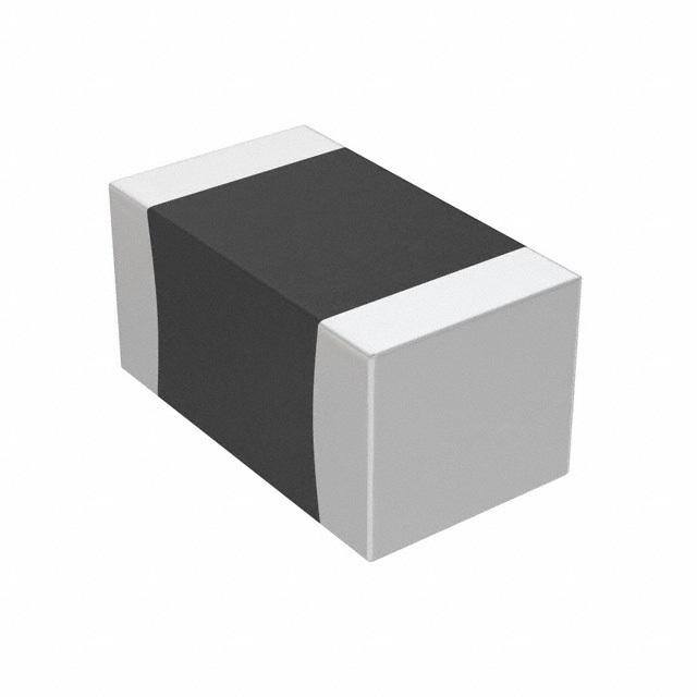
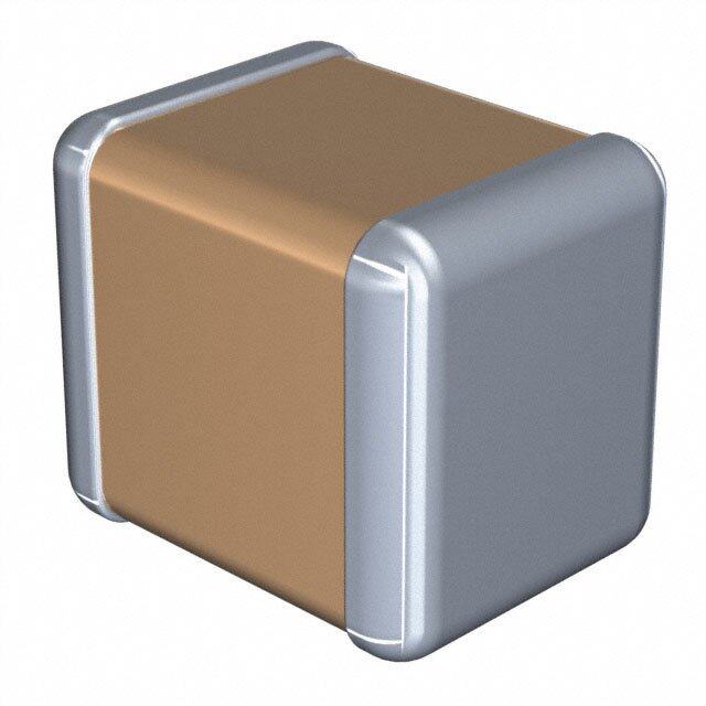
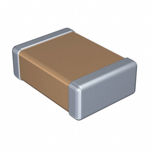
| 产品图片 |
|
| rohs | RoHS 合规性豁免无铅 / 符合限制有害物质指令(RoHS)规范要求 |
| 产品系列 | MLCC,多层陶瓷电容器MLCC - SMD/SMT,Yageo CC0603JRNPO9BN151CC |
| 数据手册 | |
| 产品型号 | CC0603JRNPO9BN151 |
| 产品 | General Type MLCCs |
| 产品培训模块 | http://www.digikey.cn/PTM/IndividualPTM.page?site=cn&lang=zhs&ptm=5466 |
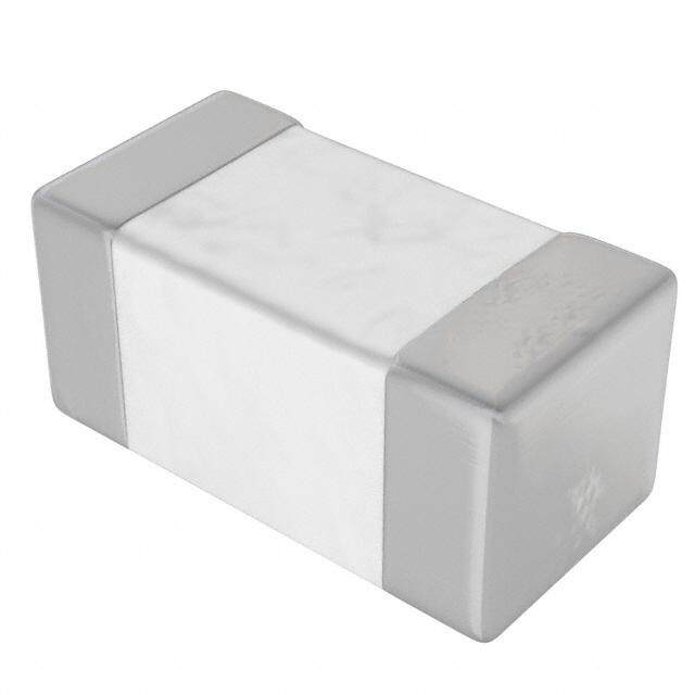
| 产品目录绘图 |
|
| 产品目录页面 | |
| 产品种类 | 多层陶瓷电容器MLCC - SMD/SMT |
| 其它名称 | 311-1071-1 |
| 包装 | 剪切带 (CT) |
| 厚度(最大值) | 0.035"(0.90mm) |
| 商标 | Yageo |
| 外壳代码-in | 0603 |
| 外壳代码-mm | 1608 |
| 外壳宽度 | 0.8 mm |
| 外壳长度 | 1.6 mm |
| 大小/尺寸 | 0.063" 长 x 0.031" 宽(1.60mm x 0.80mm) |
| 安装类型 | 表面贴装,MLCC |
| 容差 | ±5% |
| 封装 | Reel |
| 封装/外壳 | 0603(1608 公制) |
| 封装/箱体 | 0603 (1608 metric) |
| 工作温度 | -55°C ~ 125°C |
| 工作温度范围 | - 55 C to + 125 C |
| 工厂包装数量 | 4000 |
| 应用 | 通用 |
| 引线形式 | - |
| 引线间距 | - |
| 最大工作温度 | + 125 C |
| 最小工作温度 | - 55 C |
| 标准包装 | 1 |
| 温度系数 | C0G,NP0 |
| 温度系数/代码 | +/- 30 PPM / C |
| 特性 | - |
| 电介质 | C0G (NP0) |
| 电压-额定 | 50V |
| 电压额定值DC | 50 V |
| 电容 | 150pF |
| 端接类型 | SMD/SMT |
| 等级 | - |
| 类型 | Multilayer Ceramic Chip Capacitor |
| 高度-安装(最大值) | - |


- 商务部:美国ITC正式对集成电路等产品启动337调查
- 曝三星4nm工艺存在良率问题 高通将骁龙8 Gen1或转产台积电
- 太阳诱电将投资9.5亿元在常州建新厂生产MLCC 预计2023年完工
- 英特尔发布欧洲新工厂建设计划 深化IDM 2.0 战略
- 台积电先进制程称霸业界 有大客户加持明年业绩稳了
- 达到5530亿美元!SIA预计今年全球半导体销售额将创下新高
- 英特尔拟将自动驾驶子公司Mobileye上市 估值或超500亿美元
- 三星加码芯片和SET,合并消费电子和移动部门,撤换高东真等 CEO
- 三星电子宣布重大人事变动 还合并消费电子和移动部门
- 海关总署:前11个月进口集成电路产品价值2.52万亿元 增长14.8%


PDF Datasheet 数据手册内容提取
DATA SHEET SURFACE-MOUNT CERAMIC MULTILAYER CAPACITORS General purpose Class 1, NP0 16 V TO 50 V 0.22 pF to 100 nF RoHS compliant & Halogen Free 6 1 V. 7 1 0 2 7, h c r a M – n o ati cific e p S ct u d ro P
Surface-Mo unt Ceramic Multilayer Capacitors General Purpose NP0 1 6 PVro tdouc 5t 0sp eVc ification 124 SCOPE ORDERING INFORMATION - GLOBAL PART N UMBER, PHYCOMP This specifica tion describes NP0 CTC & 12NC series chip ca pacitors with lead- All part numbers are identified by the series, size, tolerance, TC material, free terminat ions. packing style, voltage, process code, termination and capacitance value. YYAAGGEEOO BBRRAANNDD oorrddeerriinngg ccooddee APPLICATIO NS GLOBAL PART NUMBER (PREFERRED) Consumer electronics for example CC XXXX X X NPO X BN XXX (1) (2) (3) (4) (5) - Tuners - Television receivers (1) SIZE – INCH BA SED (METRIC) - All types of cameras 0201 (0603) Telecommunications 0402 (1005) Data processing 0603 (1608) 0805 (2012) FEATURES 1206 (3216) Supplied in tape on reel 1210 (3225) Nickel-barrier end termination 1812 (4532) RoHS compliant (2) TOLERANCE Halogen Free compliant B = ±0.1 pF C = ±0.25 pF D = ±0.5 pF F = ±1% G = ±2% J = ±5% K = ±10% (3) PACKING STYLE R = Paper/PE taping reel; Reel 7 inch K = Blister taping reel; Reel 7 inch P = Paper/PE taping reel; Reel 13 inch F = Blister taping reel; Reel 13 inch C = Bulk case (4) RATED VOLTAGE 7 = 16 V 8 = 25 V 9 = 50 V (5) CAPACITANCE VALUE 2 significant digits+number of zeros The 3rd digit signifies the multiplying factor, and letter R is decimal point Example: 121 = 12 x 101 = 120 pF www.yageo.com Mar. 07, 2017 V.1 6
Surface-Mo unt Ceramic Multilayer Capacitors General Purpose NP0 1 6 PVro tdouc 5t 0sp eVc ification 134 CONSTRUCT ION The capacitor consists of a rectangular b lock of ceramic dielectric in which a number of interleaved metal electrodes are contained. This structure gives rise to a high capacitance per unit volu me. The inner electrodes are connected to the two end terminations and finally covered with a layer of plated tin (NiSn). The terminations are lead-free. Fig. 1 Surface mounted multilayer cerami c capacitor construction A cross section of the structure is shown in Fig.1. DIMENSION OOUUTTLLIINNEESS Table 1 For outlines see fig. 2 TY PE L1 (mm) W (mm) T (MM) Lm2i n/ .L 3 (mmmax). L4 (mmmin). F or dimension see Table 1 0201 0.6 ±0.03 0.3 ±0.03 0.10 0.20 0.20 0402 1.0 ±0.05 0.5 ±0.05 0.20 0.30 0.40 0603 1.6 ±0.10 0.8 ±0.10 0.20 0.60 0.40 2.0 ±0.10 (1) 1.25 ±0.10 (1) 0805 Refer to 0.25 0.75 0.70 2.0 ±0.20 (2) 1.25 ±0.20 (2) table 2 to 5 1206 33..22 ±±00..1350 ((12)) 11..66 ±±00..1250 ((12)) 0.25 0.75 1.40 Fig. 2 Surface 1210 3.2 ±0.20 2.5 ±0.20 0.25 0.75 1.40 mapoaucnittoerd d mi mueltnilsaiyoenr ceramic c 1812 4.5 ±0.20 3.2 ±0.20 0.25 0.75 2.20 NOTE 1. Dimension for size 0805 and 1206, C ≤ 1 nF 2. Dimension for size 0805 and 1206, C > 1 nF www.yageo.com Mar. 07, 2017 V.1 6
Surface-Mo unt Ceramic Multilayer Capacitors General Purpose NP0 1 6 PVro tdouc 5t 0sp eVc ification 144 CAPACITAN CE RANGE & THICKNESS FOR NP0 Table 2 Size s from 0201 to 0603 CAP. 0201 0402 0603 25 V 50 V 16 V 25 V 50 V 16 V 25 V 50 V 0.22 pF 0.3±0.03 0.3±0.03 0.47 pF 0.3±0.03 0.3±0.03 0.5±0.05 0.5±0.05 0.5±0.05 0.8±0.1 0.8±0.1 0.8±0.1 0.82 pF 0.3±0.03 0.3±0.03 0.5±0.05 0.5±0.05 0.5±0.05 0.8±0.1 0.8±0.1 0.8±0.1 1.0 pF 0.3±0.03 0.3±0.03 0.5±0.05 0.5±0.05 0.5±0.05 0.8±0.1 0.8±0.1 0.8±0.1 1.2 pF 0.3±0.03 0.3±0.03 0.5±0.05 0.5±0.05 0.5±0.05 0.8±0.1 0.8±0.1 0.8±0.1 1.5 pF 0.3±0.03 0.3±0.03 0.5±0.05 0.5±0.05 0.5±0.05 0.8±0.1 0.8±0.1 0.8±0.1 1.8 pF 0.3±0.03 0.3±0.03 0.5±0.05 0.5±0.05 0.5±0.05 0.8±0.1 0.8±0.1 0.8±0.1 2.2 pF 0.3±0.03 0.3±0.03 0.5±0.05 0.5±0.05 0.5±0.05 0.8±0.1 0.8±0.1 0.8±0.1 2.7 pF 0.3±0.03 0.3±0.03 0.5±0.05 0.5±0.05 0.5±0.05 0.8±0.1 0.8±0.1 0.8±0.1 3.3 pF 0.3±0.03 0.3±0.03 0.5±0.05 0.5±0.05 0.5±0.05 0.8±0.1 0.8±0.1 0.8±0.1 3.9 pF 0.3±0.03 0.3±0.03 0.5±0.05 0.5±0.05 0.5±0.05 0.8±0.1 0.8±0.1 0.8±0.1 4.7 pF 0.3±0.03 0.3±0.03 0.5±0.05 0.5±0.05 0.5±0.05 0.8±0.1 0.8±0.1 0.8±0.1 5.6 pF 0.3±0.03 0.3±0.03 0.5±0.05 0.5±0.05 0.5±0.05 0.8±0.1 0.8±0.1 0.8±0.1 6.8 pF 0.3±0.03 0.3±0.03 0.5±0.05 0.5±0.05 0.5±0.05 0.8±0.1 0.8±0.1 0.8±0.1 8.2 pF 0.3±0.03 0.3±0.03 0.5±0.05 0.5±0.05 0.5±0.05 0.8±0.1 0.8±0.1 0.8±0.1 10 pF 0.3±0.03 0.3±0.03 0.5±0.05 0.5±0.05 0.5±0.05 0.8±0.1 0.8±0.1 0.8±0.1 12 pF 0.3±0.03 0.3±0.03 0.5±0.05 0.5±0.05 0.5±0.05 0.8±0.1 0.8±0.1 0.8±0.1 15 pF 0.3±0.03 0.3±0.03 0.5±0.05 0.5±0.05 0.5±0.05 0.8±0.1 0.8±0.1 0.8±0.1 18 pF 0.3±0.03 0.3±0.03 0.5±0.05 0.5±0.05 0.5±0.05 0.8±0.1 0.8±0.1 0.8±0.1 22 pF 0.3±0.03 0.3±0.03 0.5±0.05 0.5±0.05 0.5±0.05 0.8±0.1 0.8±0.1 0.8±0.1 27 pF 0.3±0.03 0.3±0.03 0.5±0.05 0.5±0.05 0.5±0.05 0.8±0.1 0.8±0.1 0.8±0.1 33 pF 0.3±0.03 0.3±0.03 0.5±0.05 0.5±0.05 0.5±0.05 0.8±0.1 0.8±0.1 0.8±0.1 39 pF 0.3±0.03 0.3±0.03 0.5±0.05 0.5±0.05 0.5±0.05 0.8±0.1 0.8±0.1 0.8±0.1 47 pF 0.3±0.03 0.3±0.03 0.5±0.05 0.5±0.05 0.5±0.05 0.8±0.1 0.8±0.1 0.8±0.1 56 pF 0.3±0.03 0.3±0.03 0.5±0.05 0.5±0.05 0.5±0.05 0.8±0.1 0.8±0.1 0.8±0.1 68 pF 0.3±0.03 0.3±0.03 0.5±0.05 0.5±0.05 0.5±0.05 0.8±0.1 0.8±0.1 0.8±0.1 82 pF 0.3±0.03 0.3±0.03 0.5±0.05 0.5±0.05 0.5±0.05 0.8±0.1 0.8±0.1 0.8±0.1 100 pF 0.3±0.03 0.3±0.03 0.5±0.05 0.5±0.05 0.5±0.05 0.8±0.1 0.8±0.1 0.8±0.1 NOTE 1. Values in shaded cells indicate thickness class in mm 2. Capacitance value of non E-12 series is on request www.yageo.com Mar. 07, 2017 V.1 6
Surface-Mo unt Ceramic Multilayer Capacitors General Purpose NP0 1 6 PVro tdouc 5t 0sp eVc ification 154 CAPACITAN CE RANGE & THICKNESS FOR NP0 Table 3 Size s from 0201 to 0603 (continued) CAP. 0201 0402 0603 25 V 50 V 16 V 25 V 50 V 16 V 25 V 50 V 120 pF 0.5±0.05 0.5±0.05 0.5±0.05 0.8±0.1 0.8±0.1 0.8±0.1 150 pF 0.5±0.05 0.5±0.05 0.5±0.05 0.8±0.1 0.8±0.1 0.8±0.1 180 pF 0.5±0.05 0.5±0.05 0.5±0.05 0.8±0.1 0.8±0.1 0.8±0.1 220 pF 0.5±0.05 0.5±0.05 0.5±0.05 0.8±0.1 0.8±0.1 0.8±0.1 270 pF 0.5±0.05 0.5±0.05 0.5±0.05 0.8±0.1 0.8±0.1 0.8±0.1 330 pF 0.5±0.05 0.5±0.05 0.5±0.05 0.8±0.1 0.8±0.1 0.8±0.1 390 pF 0.5±0.05 0.5±0.05 0.5±0.05 0.8±0.1 0.8±0.1 0.8±0.1 470 pF 0.5±0.05 0.5±0.05 0.5±0.05 0.8±0.1 0.8±0.1 0.8±0.1 560 pF 0.5±0.05 0.5±0.05 0.5±0.05 0.8±0.1 0.8±0.1 0.8±0.1 680 pF 0.5±0.05 0.5±0.05 0.5±0.05 0.8±0.1 0.8±0.1 0.8±0.1 820 pF 0.8±0.1 0.8±0.1 0.8±0.1 1.0 nF 0.5±0.05 0.5±0.05 0.5±0.05 0.8±0.1 0.8±0.1 0.8±0.1 1.2 nF 0.8±0.1 0.8±0.1 0.8±0.1 1.5 nF 0.8±0.1 0.8±0.1 0.8±0.1 1.8 nF 0.8±0.1 0.8±0.1 0.8±0.1 2.2 nF 0.8±0.1 0.8±0.1 0.8±0.1 2.7 nF 0.8±0.1 0.8±0.1 0.8±0.1 3.3 nF 0.8±0.1 0.8±0.1 0.8±0.1 3.9 nF 0.8±0.1 0.8±0.1 0.8±0.1 4.7 nF 5.6 nF 6.8 nF 8.2 nF 10 nF 0.8±0.1 0.8±0.1 0.8±0.1 12 nF 15 nF 18 nF 22 nF 33 nF NOTE 1. Values in shaded cells indicate thickness class in mm 2. Capacitance value of non E-12 series is on request www.yageo.com Mar. 07, 2017 V.1 6
Surface-Mo unt Ceramic Multilayer Capacitors General Purpose NP0 1 6 PVro tdouc 5t 0sp eVc ification 164 CAPACITAN CE RANGE & THICKNESS FOR NP0 Table 4 Size s from 0805 to 1812 CAP. 0805 1206 1210 1812 16 V 25 V 50 V 16 V 25 V 50 V 25 V 50 V 50 V 0.22 pF 0.47 pF 0.6±0.1 0.6±0.1 0.6±0.1 0.6±0.1 0.6±0.1 0.6±0.1 0.82 pF 0.6±0.1 0.6±0.1 0.6±0.1 0.6±0.1 0.6±0.1 0.6±0.1 1.0 pF 0.6±0.1 0.6±0.1 0.6±0.1 0.6±0.1 0.6±0.1 0.6±0.1 1.2 pF 0.6±0.1 0.6±0.1 0.6±0.1 0.6±0.1 0.6±0.1 0.6±0.1 1.5 pF 0.6±0.1 0.6±0.1 0.6±0.1 0.6±0.1 0.6±0.1 0.6±0.1 1.8 pF 0.6±0.1 0.6±0.1 0.6±0.1 0.6±0.1 0.6±0.1 0.6±0.1 2.2 pF 0.6±0.1 0.6±0.1 0.6±0.1 0.6±0.1 0.6±0.1 0.6±0.1 2.7 pF 0.6±0.1 0.6±0.1 0.6±0.1 0.6±0.1 0.6±0.1 0.6±0.1 3.3 pF 0.6±0.1 0.6±0.1 0.6±0.1 0.6±0.1 0.6±0.1 0.6±0.1 3.9 pF 0.6±0.1 0.6±0.1 0.6±0.1 0.6±0.1 0.6±0.1 0.6±0.1 4.7 pF 0.6±0.1 0.6±0.1 0.6±0.1 0.6±0.1 0.6±0.1 0.6±0.1 5.6 pF 0.6±0.1 0.6±0.1 0.6±0.1 0.6±0.1 0.6±0.1 0.6±0.1 6.8 pF 0.6±0.1 0.6±0.1 0.6±0.1 0.6±0.1 0.6±0.1 0.6±0.1 8.2 pF 0.6±0.1 0.6±0.1 0.6±0.1 0.6±0.1 0.6±0.1 0.6±0.1 10 pF 0.6±0.1 0.6±0.1 0.6±0.1 0.6±0.1 0.6±0.1 0.6±0.1 12 pF 0.6±0.1 0.6±0.1 0.6±0.1 0.6±0.1 0.6±0.1 0.6±0.1 15 pF 0.6±0.1 0.6±0.1 0.6±0.1 0.6±0.1 0.6±0.1 0.6±0.1 18 pF 0.6±0.1 0.6±0.1 0.6±0.1 0.6±0.1 0.6±0.1 0.6±0.1 22 pF 0.6±0.1 0.6±0.1 0.6±0.1 0.6±0.1 0.6±0.1 0.6±0.1 27 pF 0.6±0.1 0.6±0.1 0.6±0.1 0.6±0.1 0.6±0.1 0.6±0.1 33 pF 0.6±0.1 0.6±0.1 0.6±0.1 0.6±0.1 0.6±0.1 0.6±0.1 39 pF 0.6±0.1 0.6±0.1 0.6±0.1 0.6±0.1 0.6±0.1 0.6±0.1 47 pF 0.6±0.1 0.6±0.1 0.6±0.1 0.6±0.1 0.6±0.1 0.6±0.1 1.25±0.2 1.25±0.2 56 pF 0.6±0.1 0.6±0.1 0.6±0.1 0.6±0.1 0.6±0.1 0.6±0.1 1.25±0.2 1.25±0.2 1.25±0.2 68 pF 0.6±0.1 0.6±0.1 0.6±0.1 0.6±0.1 0.6±0.1 0.6±0.1 1.25±0.2 1.25±0.2 1.25±0.2 82 pF 0.6±0.1 0.6±0.1 0.6±0.1 0.6±0.1 0.6±0.1 0.6±0.1 1.25±0.2 1.25±0.2 1.25±0.2 100 pF 0.6±0.1 0.6±0.1 0.6±0.1 0.6±0.1 0.6±0.1 0.6±0.1 1.25±0.2 1.25±0.2 1.25±0.2 NOTE 1. Values in shaded cells indicate thickness class in mm 2. Capacitance value of non E-12 series is on request www.yageo.com Mar. 07, 2017 V.1 6
Surface-Mo unt Ceramic Multilayer Capacitors General Purpose NP0 1 6 PVro tdouc 5t 0sp eVc ification 174 CAPACITAN CE RANGE & THICKNESS FOR NP0 Table 5 Size s from 0805 to 1812 (continued) C AP. 0805 1206 1210 1812 16 V 25 V 50 V 16 V 25 V 50 V 25 V 50 V 50 V 120 pF 0.6±0.1 0.6±0.1 0.6±0.1 0.6±0.1 0.6±0.1 0.6±0.1 1.25±0.2 1.25±0.2 1.25±0.2 150 pF 0.6±0.1 0.6±0.1 0.6±0.1 0.6±0.1 0.6±0.1 0.6±0.1 1.25±0.2 1.25±0.2 1.25±0.2 180 pF 0.6±0.1 0.6±0.1 0.6±0.1 0.6±0.1 0.6±0.1 0.6±0.1 1.25±0.2 1.25±0.2 1.25±0.2 220 pF 0.6±0.1 0.6±0.1 0.6±0.1 0.6±0.1 0.6±0.1 0.6±0.1 1.25±0.2 1.25±0.2 1.25±0.2 270 pF 0.6±0.1 0.6±0.1 0.6±0.1 0.6±0.1 0.6±0.1 0.6±0.1 1.25±0.2 1.25±0.2 1.25±0.2 330 pF 0.6±0.1 0.6±0.1 0.6±0.1 0.6±0.1 0.6±0.1 0.6±0.1 1.25±0.2 1.25±0.2 1.25±0.2 390 pF 0.6±0.1 0.6±0.1 0.6±0.1 0.6±0.1 0.6±0.1 0.6±0.1 1.25±0.2 1.25±0.2 1.25±0.2 470 pF 0.6±0.1 0.6±0.1 0.6±0.1 0.6±0.1 0.6±0.1 0.6±0.1 1.25±0.2 1.25±0.2 1.25±0.2 560 pF 0.6±0.1 0.6±0.1 0.6±0.1 0.6±0.1 0.6±0.1 0.6±0.1 1.25±0.2 1.25±0.2 1.25±0.2 680 pF 0.6±0.1 0.6±0.1 0.6±0.1 0.6±0.1 0.6±0.1 0.6±0.1 1.25±0.2 1.25±0.2 1.25±0.2 820 pF 0.6±0.1 0.6±0.1 0.6±0.1 0.6±0.1 0.6±0.1 0.6±0.1 1.25±0.2 1.25±0.2 1.25±0.2 1.0 nF 0.6±0.1 0.6±0.1 0.6±0.1 0.6±0.1 0.6±0.1 0.6±0.1 1.25±0.2 1.25±0.2 1.25±0.2 1.2 nF 0.85±0.1 0.85±0.1 0.85±0.1 0.6±0.1 0.6±0.1 0.6±0.1 1.25±0.2 1.25±0.2 1.25±0.2 1.5 nF 0.85±0.1 0.85±0.1 0.85±0.1 0.6±0.1 0.6±0.1 0.6±0.1 1.25±0.2 1.25±0.2 1.25±0.2 1.8 nF 0.85±0.1 0.85±0.1 0.85±0.1 0.6±0.1 0.6±0.1 0.6±0.1 1.25±0.2 1.25±0.2 1.25±0.2 2.2 nF 1.25±0.2 1.25±0.2 1.25±0.2 0.6±0.1 0.6±0.1 0.6±0.1 1.25±0.2 1.25±0.2 1.25±0.2 2.7 nF 1.25±0.2 1.25±0.2 1.25±0.2 0.6±0.1 0.6±0.1 0.6±0.1 1.25±0.2 1.25±0.2 1.25±0.2 3.3 nF 1.25±0.2 1.25±0.2 1.25±0.2 0.85±0.1 0.85±0.1 0.85±0.1 1.25±0.2 1.25±0.2 1.25±0.2 3.9 nF 1.25±0.2 1.25±0.2 1.25±0.2 0.85±0.1 0.85±0.1 0.85±0.1 1.25±0.2 1.25±0.2 1.25±0.2 4.7 nF 1.25±0.2 1.25±0.2 1.25±0.2 0.85±0.1 0.85±0.1 0.85±0.1 1.25±0.2 1.25±0.2 1.25±0.2 5.6 nF 1.25±0.2 1.25±0.2 1.25±0.2 0.85±0.1 0.85±0.1 0.85±0.1 1.25±0.2 1.25±0.2 1.25±0.2 6.8 nF 1.25±0.2 1.25±0.2 1.25±0.2 0.85±0.1 0.85±0.1 0.85±0.1 1.25±0.2 1.25±0.2 1.25±0.2 8.2 nF 1.25±0.2 1.25±0.2 1.25±0.2 1.25±0.2 1.25±0.2 1.25±0.2 1.25±0.2 1.25±0.2 1.25±0.2 0.85±0.1 0.85±0.1 0.85±0.1 10 nF 1.25±0.2 1.25±0.2 1.25±0.2 1.25±0.2 1.25±0.2 1.25±0.2 1.25±0.2 1.25±0.2 1.25±0.2 12 nF 1.25±0.2 1.25±0.2 1.25±0.2 1.25±0.2 15 nF 1.25±0.2 1.25±0.2 1.25±0.2 1.25±0.2 18 nF 1.25±0.2 1.25±0.2 1.25±0.2 1.25±0.2 22 nF 1.25±0.2 1.25±0.2 1.25±0.2 2.0±0.2 2.0±0.2 1.25±0.2 33 nF 0.85±0.1 0.85±0.1 0.85±0.1 47 nF 1.15±0.2 1.15±0.2 1.15±0.2 1.60±0.2 1.60±0.2 56 nF 68 nF 1.60±0.2 1.60±0.2 1.60±0.2 82 nF 100 nF 1.60±0.2 1.60±0.2 1.60±0.2 NOTE 1. Values in shaded cells indicate thickness class in mm 2. Capacitance value of non E-12 series is on request www.yageo.com Mar. 07, 2017 V.1 6
Surface-Mo unt Ceramic Multilayer Capacitors General Purpose NP0 1 6 PVro tdouc 5t 0sp eVc ification 184 THICKNESS CLASSES AND PACKING QUANTITY Table 6 Ø180 MM / 7 INCH Ø 330 MM / 13 INCH SIZ E THICKNESS TAPE WIDTH QUANTITY CODE CL ASSIFICATION QUANTITY PER REEL Paper Blister Paper Blister PER BULK CASE 0201 0.3 ±0.03 mm 8 mm 15,000 --- 50,000 --- --- 0402 0.5 ±0.05 mm 8 mm 10,000 --- 50,000 --- 50,000 0603 0.8 ±0.1 mm 8 mm 4,000 --- 15,000 --- 15,000 0.6 ±0.1 mm 8 mm 4,000 --- 20,000 --- 10,000 0805 0.85 ±0.1 mm 8 mm 4,000 --- 15,000 --- 8,000 1.25 ±0.2 mm 8 mm --- 3,000 --- 10,000 5,000 0.6 ±0.1 mm 8 mm 4,000 --- 20,000 --- --- 0.85 ±0.1 mm 8 mm 4,000 --- 15,000 --- --- 1206 1.00 / 1.15 ±0.1 mm 8 mm --- 3,000 --- 10,000 --- 1.25 ±0.2 mm 8 mm --- 3,000 --- 10,000 --- 1.6 ±0.15 mm 8 mm --- 2,500 --- 10,000 --- 1.6 ±0.2 mm 8 mm --- 2,000 --- 10,000 --- 0.6 / 0.7 ±0.1 mm 8 mm --- 4,000 --- 15,000 --- 0.85 ±0.1 mm 8 mm --- 4,000 --- 10,000 --- 1.0 ±0.1 mm 8 mm --- 3,000 --- 10,000 --- 1.15 ±0.1 mm 8 mm --- 3,000 --- 10,000 --- 1.15 ±0.15 mm 8 mm --- 3,000 --- 10,000 --- 1210 1.25 ±0.2 mm 8 mm --- 3,000 --- --- --- 1.5 ±0.1 mm 8 mm --- 2,000 --- --- --- 1.6 / 1.9 ±0.2 mm 8 mm --- 2,000 --- --- --- 2,000 2.0 ±0.2 mm 8 mm --- --- --- --- 1,000 1,000 2.5 ±0.2 mm 8 mm --- --- --- --- 500 1.15 ±0.15 mm 12 mm --- 3,000 --- --- --- 1.25 ±0.2 mm 12 mm --- 3,000 --- --- --- 1.35 ±0.15 mm 12 mm --- 2,000 --- --- --- 1808 1.5 ±0.1 mm 12 mm --- 2,000 --- --- --- 1.6 ±0.2 mm 12 mm --- 2,000 --- --- --- 2.0 ±0.2 mm 12 mm --- 2,000 --- --- --- 0.6 / 0.85 ±0.1 mm 12 mm --- 2,000 --- --- --- 1.15 ±0.1 mm 12 mm --- 1,000 --- --- --- 1.15 ±0.15 mm 12 mm --- 1,000 --- --- --- 1.35 ±0.15 mm 12 mm --- 1,000 --- --- --- 1812 1.5 ±0.1 mm 12 mm --- 1,000 --- --- --- 1.6 ±0.2 mm 12 mm --- 1,000 --- --- --- 2.0 ±0.2 mm 12 mm --- 1,000 --- --- --- 2.5 ±0.2 mm 12 mm --- 500 --- --- --- www.yageo.com Mar. 07, 2017 V.1 6
Surface-Mo unt Ceramic Multilayer Capacitors General Purpose NP0 1 6 PVro tdouc 5t 0sp eVc ification 194 ELECTRICAL CHARACTERISTICS NNPP00 DDIIEELLEECC TTRRIICC CCAAPPAACCIITTOORRSS;; NNIISSNN TTEERRMMIINNAATTIIOONNSS Unless other wise stated all electrical values apply at an ambient temperature of 20±1 °C, an atmospheric pressure of 86 to 106 kPa, and a relative humidity of 63 to 67%. Table 7 DESCRIPTION VALUE Capacitance range 0.22 pF to 100 nF Capacitance tolerance C < 10 pF ±0.1 pF, ±0.25 pF, ±0.5 pF C ≥ 10 pF ±1%, ±2%, ±5%, ±10% Dissipation factor (D.F.) C < 30 pF ≤ 1 / ( 400 + 20C ) C ≥ 30 pF ≤ 0.1 % Insulation resistance after 1 minute at Ur (DC) Rins ≥ 10 GΩ or Rins × Cr ≥ 500 seconds whichever is less Maximum capacitance change as a function of temperature (temperature characteristic/coefficient): ±30 ppm/°C Operating temperature range: –55 °C to +125 °C Sample limits (broken lines). Requirement levels (dotted lines) Fig. 3 Typical temperature coefficient as a function of Fig. 4 Typical capacitance change with respect to temperature the capacitance at 1 V as a function of DC voltage www.yageo.com Mar. 07, 2017 V.1 6
Surface-Mo unt Ceramic Multilayer Capacitors General Purpose NP0 1 6 PVro tdouc 5t 0sp eVc ification 1104 Fig. 5 Typical tan δ as a function of temperature SOLDERING RECOMMENDATION Table 8 SOLDERING SIZE MET HOD 0201 0402 0603 0805 1206 ≥ 1210 Reflow Reflow only ≥ 0.1 µF ≥ 1.0 µF ≥ 2.2 µF ≥ 4.7 µF Reflow only Reflow/Wave --- < 0.1 µF < 1.0 µF < 2.2 µF < 4.7 µF --- www.yageo.com Mar. 07, 2017 V.1 6
Surface-Mo unt Ceramic Multilayer Capacitors General Purpose NP0 1 6 PVro tdouc 5t 0sp eVc ification 1114 TESTS AND REQUIREMENTS Table 9 Tes t procedures and requirements T EST TEST METHOD PROCEDURE REQUIREMENTS Mounting IEC 60384- 4.3 The capacitors may be mounted on printed-circuit boards No visible damage 21/22 or ceramic substrates Visual 4.4 Any applicable method using × 10 magnification In accordance with specification inspection and dimensio n check Capacitance 4.5.1 Class 1: Within specified tolerance f = 1 MHz for C ≤ 1 nF, measuring at voltage 1 V at 20 °C rms f = 1 KHz for C > 1 nF, measuring at voltage 1 V at 20 °C rms Dissipation 4.5.2 Class 1: In accordance with specification factor (D.F.) f = 1 MHz for C ≤ 1 nF , measuring at voltage 1 V at 20 °C rms f = 1 KHz for C > 1 nF, measuring at voltage 1 V at 20 °C rms Insulation 4.5.3 At U (DC) for 1 minute In accordance with specification r resistance Temperature 4.6 Capacitance shall be measured by the steps shown in the <General purpose series> coefficient following table. Class1: ∆ C/C: ±30ppm The capacitance change should be measured after 5 min at each specified temperature stage. Class2: X7R: ∆ C/C: ±15% Step Temperature(℃) Y5V: ∆ C/C: 22~-82% a 25±2 <High Capacitance series> b Lower temperature±3℃ Class2: c 25±2 X7R/X5R: ∆ C/C: ±15% Y5V: ∆ C/C: 22~-82% d Upper Temperature±2℃ e 25±2 (1) Class I Temperature Coefficient shall be calculated from the formula as below C2-C1 Temp, Coefficient = 106 [ppm/℃] C1 xΔT C1: Capacitance at step c C2: Capacitance at 125℃ ∆T: 100℃(=125℃-25℃) (2) Class II Capacitance Change shall be calculated from the formula as below C2-C1 ∆C = x 100% C1 C1: Capacitance at step c C2: Capacitance at step b or d www.yageo.com Mar. 07, 2017 V.1 6
Surface-Mo unt Ceramic Multilayer Capacitors General Purpose NP0 1 6 PVro tdouc 5t 0sp eVc ification 1124 TEST TEST METHOD PROCEDURE REQUIR EMENTS Adhesion 4.7 A force applied for 10 seconds to the line joining the Force terminations and in a plane parallel to the substrate size ≥ 0603: 5N size = 0402: 2.5N size = 0201: 1N Bond strength 4.8 Mounting in accordance with IEC 60384-22 paragraph 4.3 No visible damage of plating on end face Conditions: bending 1 mm at a rate of 1 mm/s, radius jig 5 <General purpose series> mm ∆C/C Class 1: NP0: within ±1% or 0.5 pF whichever is greater Resistance to IEC 60384- 4.9 Precondition: 150 +0/–10 °C for 1 hour, then keep for 24 Dissolution of the end face plating shall soldering heat 21/22 ±1 hours at room temperature not exceed 25% of the length of the Preheating: for size ≤ 1206: 120 °C to 150 °C for 1 minute edge concerned Preheating: for size >1206: 100 °C to 120 °C for 1 minute and 170 °C to 200 °C for 1 minute <General purpose series> Solder bath temperature: 260 ±5 °C ∆C/C Class 1: Dipping time: 10 ±0.5 seconds NP0: within ±0.5% or 0.5 pF Recovery time: 24 ±2 hours whichever is greater D.F. within initial specified value R within initial specified value ins Solderability 4.10 Preheated the temperature of 80 °C to 140 °C The solder should cover over 95% of and maintained for 30 seconds to 60 seconds. the critical area of each termination 1. Temperature: 235±5°C / Dipping time: 2 ±0.5 s 2. Temperature: 245±5°C / Dipping time: 3 ±0.5 s (lead free)Depth of immersion: 10mm Rapid change 4.11 Preconditioning; No visual damage of 150 +0/–10 °C for 1 hour, then keep for temperature 24 ±1 hours at room temperature <General purpose series> ∆C/C 5 cycles with following detail: 30 minutes at lower category temperature Class 1: 30 minutes at upper category temperature NP0: within ±1% or 1 pF whichever is greater Recovery time 24 ±2 hours D.F. meet initial specified value R meet initial specified value ins www.yageo.com Mar. 07, 2017 V.1 6
Surface-Mo unt Ceramic Multilayer Capacitors General Purpose NP0 1 6 PVro tdouc 5t 0sp eVc ification 1134 T EST TEST METHOD PROCEDURE REQUIR EMENTS D amp heat IEC 60384- 4.13 1. Preconditioning, class 2 only: No visua l damage after recovery w ith Ur load 21/22 150 +0/-10 °C /1 hour, then keep for 24 ±1 hour at room temp <General purpose series> 2. Initial measure: ∆C/C Spec: refer to initial spec C, D, IR Class 1: 3. Damp heat test: NP0: within ±2% or 1 pF 500 ±12 hours at 40 ±2 °C; whichever is greater 90 to 95% R.H. 1.0 Ur applied D.F. 4. Recovery: Class 1: Class 1: 6 to 24 hours NP0: ≤ 2 x specified value 5. Final measure: C, D, IR R ins Class 1: P.S. If the capacitance value is le ss than the minimum value NP0: ≥ 2,500 MΩ or R x C ≥ 25s ins r permitted, then after the other measurements have been whichever is less made the capacitor shall be preconditioned according to “IEC 60384 4.1” and then the requirement shall be met. Endurance 4.14 1. Preconditioning, class 2 only: No visual damage 150 +0/-10 °C /1 hour, then keep for 24 ±1 hour at room temp <General purpose series> 2. Initial measure: ∆C/C Spec: refer to initial spec C, D, IR Class1: 3. Endurance test: NP0: within ±2% or 1 pF Temperature: NP0: 125 °C whichever is greater Specified stress voltage applied for 1,000 hours: D.F. Applied 2.0 x Ur for general product. Class1: 4. Recovery time: 24 ±2 hours NP0: ≤ 2 x specified value 5. Final measure: C, D, IR R ins Class1: P.S. If the capacitance value is less than the minimum value NP0: ≥ 4,000 MΩ or R x C ≥ 40s ins r permitted, then after the other measurements have been whichever is less made the capacitor shall be preconditioned according to “IEC 60384 4.1” and then the requirement shall be met. Voltage proof IEC 60384-1 4.6 Specified stress voltage applied for 1 minute No breakdown or flashover U ≤ 100 V: series applied 2.5 U r r 100 V < U ≤ 200 V series applied (1.5 U + 100) r r 200 V < U ≤ 500 V series applied (1.3 U + 100) r r U > 500 V: 1.3 U r r I: 7.5 mA www.yageo.com Mar. 07, 2017 V.1 6
Surface-Mo unt Ceramic Multilayer Capacitors General Purpose NP0 1 6 PVro tdouc 5t 0sp eVc ification 1144 REVISION H I STORY REVISION DATE CHANGE DESCRIPTION NOTIFICATION Version 16 Mar. 7, 2017 - - 0805 L4 spec updated Version 15 Nov. 21, 2016 - - Product range updated Version 14 Jul. 22, 2016 - - Add 0805/8.2nF and 10nF/ 16V to 50V, T=1.25mm Version 13 May. 16, 2016 - - Product range updated Version 12 Feb. 16, 2016 - - Product range updated Version 11 Sep. 11, 2014 - - Product range updated Version 10 Feb. 18, 2014 - - Product range updated Version 9 Jun. 17, 2013 - - Product range updated Version 8 Aug 05, 2011 - - Dimension updated - Size1210 T=1.0mm SPQ added Version 7 Jun 14, 2011 - - Dimension updated Version 6 Jan 06, 2011 - - Dimension updated Version 5 Dec 29, 2010 - - Dimension updated Version 4 Nov 23, 2010 - - Dimension updated Version 3 Apr 20, 2010 - - The statement of "Halogen Free" on the cover added - Dimension updated Version 2 Oct 26, 2009 - - Typo updated Version 1 Jun 02, 2009 - - 12NC code updated Version 0 Apr 15, 2009 - - New datasheet for general purpose NP0 series with RoHS compliant - Replace the "16V to 50V" part of pdf files: NP0_16V_7, NP0_16V-to- 100V_6, NP0_25V_7, NP0_50-to-500V_11 - Combine 0201 from pdf files: UP-NP0X5RX7RY5V_0201_6.3-to-50V_2 and UY-NPOX5RX7RY5V_0201_6.3-to-50V_2 - Define global part number - Description of "Halogen Free compliant" added - Test method and procedure updated www.yageo.com Mar. 07, 2017 V.1 6
Mouser Electronics Authorized Distributor Click to View Pricing, Inventory, Delivery & Lifecycle Information: Y ageo: CC0402BRNPO9BN1R0 CC0402BRNPO9BNR68 CC0402BRNPO9BN1R5 CC0402JRNPO9BN121 CC0402JRNPO9BN120 CC0402JRNPO9BN101 CC0402JRNPO9BN100 CC0402DRNPO9BN5R6 CC0402JRNPO9BN180 CC0402CRNPO9BN4R7 CC0402CRNPO9BN3R3 CC0402CRNPO9BN2R2 CC0402CRNPO9BN1R0 CC0402JRNPO9BN150 CC0402JRNPO9BN680 CC0402JRNPO9BN470 CC0402JRNPO9BN390 CC0402JRNPO9BN330 CC0402JRNPO9BN270 CC0402JRNPO9BN221 CC0402JRNPO9BN220 CC0603JRNPO9BN221 CC0603JRNPO9BN181 CC0603JRNPO9BN271 CC0603JRNPO9BN151 CC0603JRNPO9BN331 CC0603JRNPO9BN121 CC0603JRNPO9BN101 CC0603JRNPO8BN102 CC0603JRNPO9BN681 CC0805JRNPO9BN151 CC0805JRNPO9BN101 CC0805JRNPO9BN330 CC0805JRNPO9BN681 CC0805JRNPO9BN471 CC0805JRNPO9BN102 CC0805JRNPO9BN331 CC0805JRNPO9BN120 CC0805JRNPO9BN271 CC0805JRNPO9BN270 CC0805JRNPO9BN221 CC0805JRNPO9BN181 CC0805JRNPO9BN152 CC0805BPNPO9BN2R2 CC0805JRNPO9BN821 CC0805JRNPO9BN561 CC1206JRNPO8BN103 CC1206JRNPO9BN102 CC1206JRNPO9BN222 CC0805JRNPO9BN470 CC0603CRNPO9BN4R7 CC0805JRNPO9BN100 CC0603CRNPO9BN2R2 CC0603FRNPO9BN150 CC0603CRNPO9BN3R3 CC0603CRNPO9BN1R8 CC0603BRNPO9BN6R8 CC0603BRNPO9BN3R3 CC0603BRNPO9BN2R0 CC0805JRNPO9BN680 CC0805JRNPO9BN220 CC0805JRNPO9BN150 CC1206JRNPO9BN101 CC0603CRNPO9BN2R0 CC0603CRNPO9BN3R0 CC0603JRNPO9BN160 CC0402BRNPO9BN1R6 CC0402BRNPO9BN1R1 CC0402BRNPO9BN8R0 CC0402BRNPO9BN7R5 CC0402FPNPO9BN470 CC0603FPNPO9BN150 CC0603FPNPO9BN270 CC0603FPNPO9BN820 CC0603GPNPO9BN120 CC0603GPNPO9BN331 CC0603GPNPO9BN390 CC0603GPNPO9BN471 CC0603GPNPO9BN680 CC0805BPNPO9BN1R0 CC0805BPNPO9BN5R6 CC0805BPNPO9BN8R2 CC0805BPNPO9BNR47 CC0805CPNPO9BN6R8 CC0805CRNPO9BNR56 CC0805DRNPO9BN8R2 CC0805FPNPO9BN180 CC0805FPNPO9BN270 CC0805FRNPO9BN391 CC0805GKNPO8BN332 CC0805GKNPO9BN272 CC0805GPNPO9BN150 CC0805GPNPO9BN331 CC0805JPNPO9BN221 CC0805JPNPO9BN470 CC0805JPNPO9BN561 CC1206BRNPO9BN2R7 CC1206CRNPO9BN3R3 CC1206CRNPO9BNR56 CC1206FRNPO9BN150