ICGOO在线商城 > 开发板,套件,编程器 > 评估板 - 嵌入式 - MCU,DSP > C8051F330DK
 Datasheet下载
- 型号: C8051F330DK
- 制造商: Silicon Laboratories
- 库位|库存: xxxx|xxxx
- 要求:
| 数量阶梯 | 香港交货 | 国内含税 |
| +xxxx | $xxxx | ¥xxxx |
查看当月历史价格
查看今年历史价格
C8051F330DK产品简介:
ICGOO电子元器件商城为您提供C8051F330DK由Silicon Laboratories设计生产,在icgoo商城现货销售,并且可以通过原厂、代理商等渠道进行代购。 C8051F330DK价格参考。Silicon LaboratoriesC8051F330DK封装/规格:评估板 - 嵌入式 - MCU,DSP, C8051F33x - MCU 8-Bit 8051 Embedded Evaluation Board。您可以下载C8051F330DK参考资料、Datasheet数据手册功能说明书,资料中有C8051F330DK 详细功能的应用电路图电压和使用方法及教程。
Silicon Labs的C8051F330DK评估板是一款用于嵌入式系统的开发工具,主要针对微控制器(MCU)和数字信号处理器(DSP)的应用。该评估板基于C8051F330 MCU,这是一款高性能、低功耗的8位MCU,适用于各种工业、消费电子和通信领域。

 应用场景

1. 工业自动化与控制
   - 电机控制:C8051F330DK可以用于开发高效的电机控制系统,支持直流电机、步进电机和无刷直流电机的驱动与控制。其高精度的PWM输出和丰富的外设接口使得它能够实现精确的速度和位置控制。
   - 传感器数据采集:该评估板具备多种模拟输入通道,适合用于温度、压力、湿度等传感器的数据采集和处理。结合其内置的ADC(模数转换器),可以实现高精度的实时监测和控制。

2. 智能家居与物联网
   - 智能家电控制:C8051F330DK可以用于开发智能家电的控制系统,如智能灯泡、智能插座、智能温控器等。通过集成Wi-Fi或Zigbee模块,可以实现远程控制和自动化管理。
   - 环境监测系统:该评估板可以作为环境监测设备的核心,用于检测空气质量、光照强度、噪声水平等参数,并将数据上传到云端进行分析和展示。

3. 医疗设备
   - 便携式医疗设备:C8051F330DK的低功耗特性使其非常适合用于便携式医疗设备,如血糖仪、心率监测仪等。其高效的数据处理能力和丰富的外设接口有助于提高设备的准确性和可靠性。
   - 健康监护系统:该评估板可以用于开发个人健康监护系统,实时监测用户的生理参数,并通过无线通信技术将数据传输给医生或家人,以便及时采取措施。

4. 通信与网络
   - 协议转换器:C8051F330DK可以用于开发各种通信协议之间的转换器,如RS232到USB、SPI到I2C等。其灵活的硬件设计和强大的软件支持使得它可以适应不同的通信需求。
   - 数据网关:该评估板可以作为数据网关的核心,用于连接不同类型的传感器和执行器,实现本地数据的收集和转发,同时支持与云端平台的交互。

总之,C8051F330DK评估板凭借其高性能、低功耗和丰富的外设接口,广泛应用于工业控制、智能家居、医疗设备和通信网络等领域,为开发者提供了强大的硬件支持和灵活的开发环境。
| 参数 | 数值 |
| 产品目录 | 编程器,开发系统嵌入式解决方案 |
| 描述 | DEV KIT FOR C8051F330/F331开发板和工具包 - 8051 MCU DEVELOPMENT KIT W/ US POWER SUPPLY |
| 产品分类 | 评估板 - 嵌入式 - MCU, DSP工程工具 |
| 品牌 | Silicon LabsSilicon Laboratories Inc |
| 产品手册 | |
| 产品图片 |
|
| rohs | 符合RoHS含铅 / 不符合限制有害物质指令(RoHS)规范要求 |
| 产品系列 | 嵌入式开发工具,嵌入式处理器开发套件,开发板和工具包 - 8051,Silicon Labs C8051F330DK- |
| 数据手册 | |
| 产品型号 | C8051F330DKC8051F330DK |
| 产品 | Development Kits |
| 产品目录页面 | |
| 产品种类 | 开发板和工具包 - 8051 |
| 其它名称 | 336-1264 |
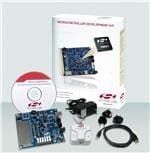
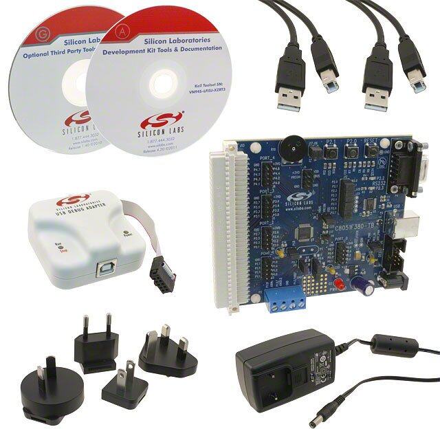
| 内容 | 板,电缆,电源,USB 调试适配器编程器 |
| 单位重量 | 50 mg |
| 商标 | Silicon Labs |
| 安装类型 | 固定 |
| 工作电源电压 | 7 V to 15 V |
| 工具用于评估 | C8051F330 |
| 平台 | - |
| 接口类型 | RS-232, USB |
| 描述/功能 | Contains everything needed to develop applications with the C8051F330 microcontroller |
| 操作系统 | - |
| 数据总线宽度 | 8 bit |
| 板类型 | 评估平台 |
| 标准包装 | 1 |
| 核心 | 8051 |
| 核心处理器 | 8051 |
| 相关产品 | /product-detail/zh/C8051F330-GM/336-1262-ND/819562/product-detail/zh/C8051F330-GP/336-1263-ND/819563/product-detail/zh/C8051F331-GM/336-1265-ND/819565/product-detail/zh/C8051F330-GMR/C8051F330-GMR-ND/990801/product-detail/zh/C8051F331-GMR/C8051F331-GMR-ND/990802 |
| 类型 | MCU 8-位 |
| 系列 | C8051F330 |
| 配套使用产品/相关产品 | C8051F33x |


- 商务部:美国ITC正式对集成电路等产品启动337调查
- 曝三星4nm工艺存在良率问题 高通将骁龙8 Gen1或转产台积电
- 太阳诱电将投资9.5亿元在常州建新厂生产MLCC 预计2023年完工
- 英特尔发布欧洲新工厂建设计划 深化IDM 2.0 战略
- 台积电先进制程称霸业界 有大客户加持明年业绩稳了
- 达到5530亿美元!SIA预计今年全球半导体销售额将创下新高
- 英特尔拟将自动驾驶子公司Mobileye上市 估值或超500亿美元
- 三星加码芯片和SET,合并消费电子和移动部门,撤换高东真等 CEO
- 三星电子宣布重大人事变动 还合并消费电子和移动部门
- 海关总署:前11个月进口集成电路产品价值2.52万亿元 增长14.8%

PDF Datasheet 数据手册内容提取
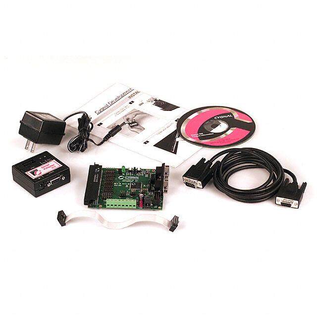
C8051F33x C8051F33X DEVELOPMENT KIT USER’S GUIDE 1. Kit Contents The C8051F33x Development Kit contains the following items: • C8051F330 Target Board • C8051Fxxx Development Kit Quick-Start Guide • AC to DC Power Adapter • USB Debug Adapter (USB to Debug Interface) • USB Cable • CD-ROM 2. Hardware Setup Using a USB Debug Adapter The target board is connected to a PC running the Silicon Laboratories IDE via the USB Debug Adapter as shown in Figure1. 1. Connect the USB Debug Adapter to the DEBUG connector on the target board with the 10-pin ribbon cable. 2. Connect one end of the USB cable to the USB connector on the USB Debug Adapter. 3. Connect the other end of the USB cable to a USB Port on the PC. 4. Connect the ac/dc power adapter to power jack P1 on the target board. Notes: • Use the Reset button in the IDE to reset the target when connected using a USB Debug Adapter. • Remove power from the target board and the USB Debug Adapter before connecting or disconnecting the ribbon cable from the target board. Connecting or disconnecting the cable when the devices have power can damage the device and/or the USB Debug Adapter. AC/DC Adapter PC USB Debug Adapter Target Board CUaSbBle StopPower Run USB DEBUG ADAPTERSilicon Laboratories P3.7 SILICONP LWARBORATMORCIEUS RESET P1.6 Port 2 Port 0 Port 1 Port 3 Port 4 Figure 1. Hardware Setup Using a USB Debug Adapter Rev. 0.7 2/14 Copyright © 2014 by Silicon Laboratories C8051F33x
C8051F33x 3. Software Setup Simplicity Studio greatly reduces development time and complexity with Silicon Labs EFM32 and 8051 MCU products by providing a high-powered IDE, tools for hardware configuration, and links to helpful resources, all in one place. Once Simplicity Studio is installed, the application itself can be used to install additional software and documentation components to aid in the development and evaluation process. Figure 2. Simplicity Studio The following Simplicity Studio components are required for the C8051F330 Development Kit: 8051 Products Part Support Simplicity Developer Platform Download and install Simplicity Studio from www.silabs.com/8bit-software or www.silabs.com/simplicity-studio. Once installed, run Simplicity Studio by selecting StartSilicon LabsSimplicity StudioSimplicity Studio from the start menu or clicking the Simplicity Studio shortcut on the desktop. Follow the instructions to install the software and click Simplicity IDE to launch the IDE. The first time the project creation wizard runs, the Setup Environment wizard will guide the user through the process of configuring the build tools and SDK selection. In the Part Selection step of the wizard, select from the list of installed parts only the parts to use during development. Choosing parts and families in this step affects the displayed or filtered parts in the later device selection menus. Choose the C8051F33x family by checking the C8051F33x check box. Modify the part selection at any time by accessing the Part Management dialog from the WindowPreferencesSimplicity StudioPart Management menu item. Simplicity Studio can detect if certain toolchains are not activated. If the Licensing Helper is displayed after completing the Setup Environment wizard, follow the instructions to activate the toolchain. 2 Rev. 0.7
C8051F33x 3.1. Running Blinky Each project has its own source files, target configuration, SDK configuration, and build configurations such as the Debug and Release build configurations. The IDE can be used to manage multiple projects in a collection called a workspace. Workspace settings are applied globally to all projects within the workspace. This can include settings such as key bindings, window preferences, and code style and formatting options. Project actions, such as build and debug are context sensitive. For example, the user must select a project in the Project Explorer view in order to build that project. To create a project based on the Blinky example: 1. Click the Simplicity IDE tile from the Simplicity Studio home screen. 2. Click the Create new project link from the welcome screen or go to FileNewSilicon Labs MCU Project. 3. In the Kit drop-down, select C8051F330 Development Kit, in the Part drop-down, select C8051F330, and in the SDK drop-down, select the desired SDK. Click Next. 4. Select Example and click Next. 5. Under C8051F330 Development Kit in the Blinky folder, select F330-5 Blinky and click Finish. 6. Click on the project in the Project Explorer and click Build, the hammer icon in the top bar. Alternatively, go to ProjectBuild Project. 7. Click Debug to download the project to the hardware and start a debug session. 8. Press the Resume button to start the code running. The LED should blink. 9. Press the Suspend button to stop the code. 10. Press the Reset the device button to reset the target MCU. 11. Press the Disconnect button to return to the development perspective. 3.2. Simplicity Studio Help Simplicity Studio includes detailed help information and device documentation within the tool. The help contains descriptions for each dialog window. To view the documentation for a dialog, click the question mark icon in the window: This will open a pane specific to the dialog with additional details. The documentation within the tool can also be viewed by going to HelpHelp Contents or HelpSearch. Rev. 0.7 3
C8051F33x 3.3. Legacy 8-bit IDE Note: Using the Simplicity Studio tools with the C8051F330 Development Kit is recommended. See section 3. "Software Setup‚" on page 2 for more information. Download the 8-bit software from the website (www.silabs.com/8bit-software) or use the provided installer on the CD-ROM to install the software tools for the C8051F33x devices. After installation, examples can be found in ...\Examples\C8051F330_5 in the installation directory. At a minimum, the C8051F330 DK requires: Silicon Labs IDE—Software enabling initial evaluation, development, and debugging. Configuration Wizard 2—Initialization code generation software for the C8051F33x devices. Keil C51 Tools—Keil 8051 Compiler/Assembler/Linker toolchain. Other software available includes: Keil µVision Driver—Driver for the Keil µVision IDE that enables development and debugging on C8051Fxxx MCUs. Flash Programming Utilities and MCU Production Programmer—Programming utilities for the production line. More information on the available programming options can be found on the website: http://www.silabs.com/products/mcu/Pages/ProgrammingOptions.aspx. ToolStick Development Tools—Software and examples for the ToolStick development platform. More information on this platform can be found at www.silabs.com/toolstick. The development kit includes the latest version of the C51 Keil 8051 toolset. This toolset is initially limited to a code size of 2kB and programs start at code address 0x0800. After registration, the code size limit is removed entirely and programs will start at code address 0x0000. To register the Keil toolset: 1. Find the Product Serial Number printed on the CD-ROM. If you no longer have this serial number, register on the Silicon Labs website (www.silabs.com/8bit-software) to obtain the serial number. 2. Open the Keil µVision4 IDE from the installation directory with administrative privileges. 3. Select FileLicense Management to open the License Management window. Figure 3. Keil µVision4 IDE License Management Window 4. Click on the Get LIC via Internet... button to open the Obtaining a License IDE Code (LIC) window. 5. Press OK to open a browser window to the Keil website. If the window doesn’t open, navigate to www.keil.com/license/install.htm. 6. Enter the Silicon Labs Product Serial Number printed on the CD-ROM, along with any additional required 4 Rev. 0.7
C8051F33x information. 7. Once the form is complete, click the Submit button. An email will be sent to the provided email address with the license activation code. 8. Copy the License ID Code (LIC) from the email. 9. Paste the LIC into the New License ID Code (LIC) text box at the bottom of the License Management window in µVision4. 10. Press the Add LIC button. The window should now list the PK51 Prof. Developers Kit for Silabs as a licensed product. 11. Click the Close button. Rev. 0.7 5
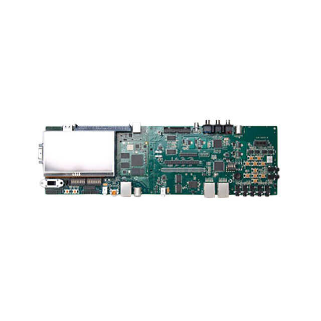
C8051F33x 4. Target Board The C8051F33x Development Kit includes a target board with a C8051F330 device pre-installed for evaluation and preliminary software development. Numerous input/output (I/O) connections are provided to facilitate prototyping using the target board. Refer to Figure4 for the locations of the various I/O connectors. P1 Power connector (accepts input from 7 to 15 VDC unregulated power adapter) J1 22-pin Expansion I/O connector J3 Port I/O Configuration Jumper Block J4 DEBUG connector for Debug Adapter interface J5 DB-9 connector for UART0 RS232 interface P2 Analog I/O terminal block J6 Connects IDAC to P0.1 pin J8 USB Debug Adapter target board power connector J9, J10 External crystal enable connectors J5 P0.7 Reset J6 J9 J3Pin 2 J10 Pin 1 P1.3 Pin 1 a e Pin 2 Ar e p J1 y ot ot Pr J8 G U C8051 B F33X E D J4 Pin 1 P1 P2 PWR Pin 1 Prototyping Area I/O Connection Points Figure 4. C8051F330 Target Board 6 Rev. 0.7
C8051F33x 4.1. System Clock Sources The C8051F330 device installed on the target board features a calibrated programmable internal oscillator which is enabled as the system clock source on reset. After reset, the internal oscillator operates at a frequency of 3.0625MHz (±2%) by default but may be configured by software to operate at other frequencies. Therefore, in many applications an external oscillator is not required. However, if you wish to operate the C8051F330 device at a frequency not available with the internal oscillator, an external crystal may be used. Refer to the C8051F33x data sheet for more information on configuring the system clock source. The target board is designed to facilitate the installation of an external crystal. Remove shorting blocks at headers J9 and J10 and install the crystal at the pads marked Y1. Install a 10M resistor at R9 and install capacitors at C14 and C15 using values appropriate for the crystal you select. Refer to the C8051F33x data sheet for more information on the use of external oscillators. 4.2. Switches and LEDs Two switches are provided on the target board. Switch SW1 is connected to the RESET pin of the C8051F330. Pressing SW1 puts the device into its hardware-reset state. Switch SW2 is connected to the C8051F330’s general purpose I/O (GPIO) pin through headers. Pressing SW2 generates a logic low signal on the port pin. Remove the shorting block from the jumper to disconnect SW2 from the port pins. The port pin signal is also routed to a pin on the J1 I/O connector. See Table1 for the port pins and headers corresponding to each switch. Two LEDs are also provided on the target board. The red LED labeled PWR is used to indicate a power connection to the target board. The green LED labeled with a port pin name is connected to the C8051F330’s GPIO pin through headers. Remove the shorting block from the jumper to disconnect the LED from the port pin. The port pin signal is also routed to a pin on the J1 I/O connector. See Table1 for the port pins and headers corresponding to each LED. Table 1. Target Board I/O Descriptions Description I/O Jumper SW1 Reset none SW2 P0.7 J3[3–4] Green LED P1.3 J3[1–2] Red LED PWR none Rev. 0.7 7
C8051F33x 4.3. Expansion I/O Connector (J1) The 22-pin Expansion I/O connector J1 provides access to all signal pins of the C8051F330 device. Pins for +3V, digital ground and the output of an on-board low-pass filter are also available. A small through-hole prototyping area is also provided. All I/O signals routed to connector J1 are also routed to through-hole connection points between J1 and the prototyping area (see Figure4 on page6). Each connection point is labeled indicating the signal available at the connection point. See Table2 for a list of pin descriptions for J1. Table 2. J1 Pin Descriptions Pin # Description Pin # Description 1 +3VD (+3.3VDC) 12 P1.1 2 IDAC 13 P1.2 3 P0.0 14 P1.3 4 P0.1 15 P1.4 5 P0.2 16 P1.5 6 P0.3 17 P1.6 7 P0.4 18 P1.7 8 P0.5 19 P2.0 9 P0.6 20 RST/C2CLK 10 P0.7 21 GND 11 P1.0 22 GND 4.4. Target Board DEBUG Interface (J4) The DEBUG connector (J4) provides access to the DEBUG (C2) pins of the C8051F330. It is used to connect the Serial Adapter or the USB Debug Adapter to the target board for in-circuit debugging and Flash programming. Table3 shows the DEBUG pin definitions. Table 3. DEBUG Connector Pin Descriptions Pin # Description 1 +3VD (+3.3VDC) 2, 3, 9 GND (Ground) 4 C2D 5 /RST (Reset) 6 P3.0 7 C2CK 8 Not Connected 10 USB Power 8 Rev. 0.7
C8051F33x 4.5. Serial Interface (J5) A RS232 transceiver circuit and DB-9 (J5) connector are provided on the target board to facilitate serial connections to UART0 of the C8051F330. The TX, RX, RTS and CTS signals of UART0 may be connected to the DB-9 connector and transceiver by installing shorting blocks on header J3. J3[5–6]- Install shorting block to connect UART0 TX (P0.4) to transceiver. J3[7–8]- Install shorting block to connect UART0 RX (P0.5) to transceiver. J3[9–10]- Install shorting block to connect UART0 RTS (P1.1) to transceiver. J3[11–12]- Install shorting block to connect UART0 CTS (P1.2) to transceiver. 4.6. Analog I/O (P2) Several of the C8051F330 target device’s port pins are connected to the J6 terminal block. Refer to Table4 for the P2 terminal block connections. Table 4. P2 Terminal Block Pin Descriptions Pin # Description 1 CNVSTR (P0.6) 2 IDAC 3 P1.5 4 P1.4 5 GND (Ground) 6 P0.0 / Vref (Voltage Reference) 4.7. IDAC Connector (J6) The C8051F330 target board also features a Current-to-Voltage 1K load resistor that may be connected to the 10-bit current-mode Digital-to-Analog Converter (IDAC) on port pin (P0.1). Install a shorting block on J6 to connect the IDAC pin of the target device to the load resistor. The IDAC signal is then routed to the J1[2] and P2[2] connectors. 4.8. USB Debug Adapter Target Board Power Connector (J8) The USB Debug Adapter includes a connection to provide power to the target board. This connection is routed from J4[10] to J8[1]. Place a shorting block at header J8[2–3] to power the board directly from an ac/dc power adapter. Place a shorting block at header J8[1–2] to power the board from the USB Debug Adapter. Please note that the second option is not supported with either the EC1 or EC2 Serial Adapters. Rev. 0.7 9
C8051F33x 5. Schematic c i t a m e h c S d r a o B t e g r a T 0 3 3 F 1 5 0 8 C . 5 e r u g i F 10 Rev. 0.7
C8051F33x DOCUMENT CHANGE LIST Revision 0.4 to Revision 0.5 Section 1, added USB Debug Adapter and USB Cable. Section 2, changed name from "Hardware Setup" to "Hardware Setup using an EC2 Serial Adapter". Section 2, added 2 Notes bullets. Section 2, removed Note from bottom of page. Added Section 3, "Hardware Setup using a USB Debug Adapter". Section 5.4.2, changed step 2 to include new instructions. Section 7, J4, changed "Serial Adapter" to "Debug Adapter". Target Board DEBUG Interface Section, added USB Debug Adapter. DEBUG Connector Pin Descriptions Table, changed pin 4 to C2D. Changed "jumper" to "header". EC2 Serial Adapter section, added EC2 to the section title, table title and figure title. EC2 Serial Adapter section, changed "JTAG" to "DEBUG". Added "USB Debug Adapter" section. Section 7, J8, changed "Serial Adapter" to "USB Debug Adapter" DEBUG Connector Pin Descriptions Table, changed pin 10 to USB Power USB Debug Adapter Target Board Power Connector (J8) Section, changed "Serial" to "USB Debug" Revision 0.5 to Revision 0.6 Removed EC2 Serial Adapter from Kit Contents. Removed Section 2. Hardware Setup using an EC2 Serial Adapter. See RS232 Serial Adapter (EC2) User's Guide. Removed Section 8. EC2 Serial Adapter. See RS232 Serial Adapter (EC2) User's Guide. Removed Section 9. USB Debug Adapter. See USB Debug Adapter User's Guide. Revision 0.6 to Revision 0.7 Updated 3. "Software Setup‚" on page 2. Rev. 0.7 11
Simplicity Studio One-click access to MCU and wireless tools, documentation, software, source code libraries & more. Available for Windows, Mac and Linux! IoT Portfolio SW/HW Quality Support and Community www.silabs.com/IoT www.silabs.com/simplicity www.silabs.com/quality community.silabs.com Disclaimer Silicon Laboratories intends to provide customers with the latest, accurate, and in-depth documentation of all peripherals and modules available for system and software implementers using or intending to use the Silicon Laboratories products. Characterization data, available modules and peripherals, memory sizes and memory addresses refer to each specific device, and "Typical" parameters provided can and do vary in different applications. Application examples described herein are for illustrative purposes only. Silicon Laboratories reserves the right to make changes without further notice and limitation to product information, specifications, and descriptions herein, and does not give warranties as to the accuracy or completeness of the included information. Silicon Laboratories shall have no liability for the consequences of use of the information supplied herein. This document does not imply or express copyright licenses granted hereunder to design or fabricate any integrated circuits. The products must not be used within any Life Support System without the specific written consent of Silicon Laboratories. A "Life Support System" is any product or system intended to support or sustain life and/or health, which, if it fails, can be reasonably expected to result in significant personal injury or death. Silicon Laboratories products are generally not intended for military applications. Silicon Laboratories products shall under no circumstances be used in weapons of mass destruction including (but not limited to) nuclear, biological or chemical weapons, or missiles capable of delivering such weapons. Trademark Information Silicon Laboratories Inc., Silicon Laboratories, Silicon Labs, SiLabs and the Silicon Labs logo, CMEMS®, EFM, EFM32, EFR, Energy Micro, Energy Micro logo and combinations thereof, "the world’s most energy friendly microcontrollers", Ember®, EZLink®, EZMac®, EZRadio®, EZRadioPRO®, DSPLL®, ISOmodem ®, Precision32®, ProSLIC®, SiPHY®, USBXpress® and others are trademarks or registered trademarks of Silicon Laboratories Inc. ARM, CORTEX, Cortex-M3 and THUMB are trademarks or registered trademarks of ARM Holdings. Keil is a registered trademark of ARM Limited. All other products or brand names mentioned herein are trademarks of their respective holders. Silicon Laboratories Inc. 400 West Cesar Chavez Austin, TX 78701 USA http://www.silabs.com