ICGOO在线商城 > 分立半导体产品 > 二极管 - 齐纳 - 单 > BZX55C6V8-TR
 Datasheet下载
- 型号: BZX55C6V8-TR
- 制造商: Vishay
- 库位|库存: xxxx|xxxx
- 要求:
| 数量阶梯 | 香港交货 | 国内含税 |
| +xxxx | $xxxx | ¥xxxx |
查看当月历史价格
查看今年历史价格
BZX55C6V8-TR产品简介:
ICGOO电子元器件商城为您提供BZX55C6V8-TR由Vishay设计生产,在icgoo商城现货销售,并且可以通过原厂、代理商等渠道进行代购。 BZX55C6V8-TR价格参考¥1.50-¥2.00。VishayBZX55C6V8-TR封装/规格:二极管 - 齐纳 - 单, Zener Diode 6.8V 500mW ±5% Through Hole DO-35。您可以下载BZX55C6V8-TR参考资料、Datasheet数据手册功能说明书,资料中有BZX55C6V8-TR 详细功能的应用电路图电压和使用方法及教程。
BZX55C6V8-TR 是由 Vishay Semiconductor Diodes Division 生产的一款单齐纳二极管,其主要应用场景包括:

1. 电压稳压:该型号的齐纳二极管常用于电路中提供稳定的参考电压。BZX55C6V8-TR 的齐纳电压为 6.8V(±5% 精度),适用于低功率电路中的电压调节。

2. 过压保护:在敏感电子设备中,BZX55C6V8-TR 可以用来防止输入电压过高对后续电路造成损害。例如,在电源输入端或信号线路上,齐纳二极管可以将电压钳位在安全范围内。

3. 信号电平转换:在需要将信号限制在特定范围内的应用中,这款齐纳二极管可以用来截断超过设定值的信号幅值,确保信号不会超出预期范围。

4. 温度补偿电路:由于 BZX55C6V8-TR 具有较低的动态电阻和良好的温度稳定性,它适合用作温度补偿元件,特别是在需要精确控制电压的场景中。

5. 电源监控电路:在一些简单的电源监控设计中,齐纳二极管可以与比较器配合使用,检测电源电压是否低于或高于某个阈值,并触发相应的保护机制。

6. 音频和射频电路中的限幅:在音频放大器或射频前端中,齐纳二极管可以用作限幅器,避免信号失真或损坏后级电路。

7. 基准电压源:尽管其精度不如专用基准电压芯片,但在低成本应用中,BZX55C6V8-TR 可作为简单的基准电压源,用于模拟电路或数字电路中的比较操作。

总之,BZX55C6V8-TR 是一款小巧、可靠且经济高效的齐纳二极管,适用于多种低功率电子设备中的电压稳定和保护功能。
| 参数 | 数值 |
| 产品目录 | |
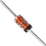
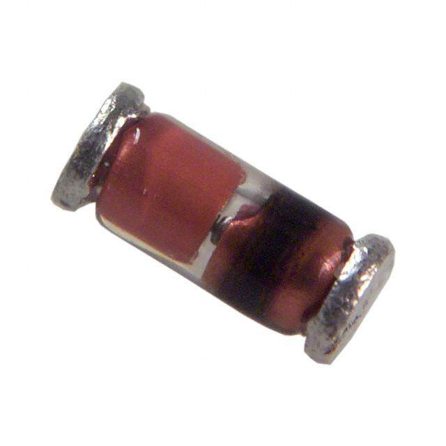
| 描述 | DIODE ZENER 500MW DO35稳压二极管 6.8 Volt 0.5 Watt 5% |
| 产品分类 | 单二极管/齐纳分离式半导体 |
| 品牌 | Vishay Semiconductor Diodes DivisionVishay Semiconductors |
| 产品手册 | |
| 产品图片 |
|
| rohs | RoHS 合规性豁免无铅 / 符合限制有害物质指令(RoHS)规范要求 |
| 产品系列 | 二极管与整流器,稳压二极管,Vishay Semiconductors BZX55C6V8-TR* |
| 数据手册 | |
| 产品型号 | BZX55C6V8-TRBZX55C6V8-TR |
| 产品种类 | |
| 功率耗散 | 500 mW |
| 商标 | Vishay Semiconductors |
| 安装风格 | Through Hole |
| 封装 | Reel |
| 封装/箱体 | DO-35 |
| 工厂包装数量 | 10000 |
| 最大反向漏泄电流 | 100 nA |
| 最大工作温度 | + 175 C |
| 最大齐纳阻抗 | 8 Ohms |
| 最小工作温度 | - 65 C |
| 标准包装 | 10,000 |
| 电压容差 | 6 % |
| 电压温度系数 | 0.05 %/K |
| 配置 | Single |
| 齐纳电压 | 6.8 V |
| 齐纳电流 | 200 mA |


- 商务部:美国ITC正式对集成电路等产品启动337调查
- 曝三星4nm工艺存在良率问题 高通将骁龙8 Gen1或转产台积电
- 太阳诱电将投资9.5亿元在常州建新厂生产MLCC 预计2023年完工
- 英特尔发布欧洲新工厂建设计划 深化IDM 2.0 战略
- 台积电先进制程称霸业界 有大客户加持明年业绩稳了
- 达到5530亿美元!SIA预计今年全球半导体销售额将创下新高
- 英特尔拟将自动驾驶子公司Mobileye上市 估值或超500亿美元
- 三星加码芯片和SET,合并消费电子和移动部门,撤换高东真等 CEO
- 三星电子宣布重大人事变动 还合并消费电子和移动部门
- 海关总署:前11个月进口集成电路产品价值2.52万亿元 增长14.8%


PDF Datasheet 数据手册内容提取
BZX55-Series www.vishay.com Vishay Semiconductors Small Signal Zener Diodes FEATURES • Very sharp reverse characteristic • Low reverse current level • Very high stability • Low noise • AEC-Q101 qualified • Material categorization: For definitions of compliance please see www.vishay.com/doc?99912 APPLICATIONS PRIMARY CHARACTERISTICS • Voltage stabilization PARAMETER VALUE UNIT V range nom. 2.4 to 75 V Z Test current I 2.5; 5 mA ZT V specification Pulse current Z Int. construction Single ORDERING INFORMATION DEVICE NAME ORDERING CODE TAPED UNITS PER REEL MINIMUM ORDER QUANTITY BZX55-series BZX55-series-TR 10 000 per 13" reel 30 000/box 10 000 per ammopack BZX55-series BZX55-series-TAP 30 000/box (52 mm tape) PACKAGE MOLDING COMPOUND MOISTURE SENSITIVITY SOLDERING PACKAGE NAME WEIGHT FLAMMABILITY RATING LEVEL CONDITIONS MSL level 1 DO-35 125 mg UL 94 V-0 260 °C/10 s at terminals (according J-STD-020) ABSOLUTE MAXIMUM RATINGS (T = 25 °C, unless otherwise specified) amb PARAMETER TEST CONDITION SYMBOL VALUE UNIT Power dissipation l = 4 mm, T = 25 °C P 500 mW L tot Zener current I P /V mA Z tot Z Junction to ambient air l = 4 mm, T = constant R 300 K/W L thJA Junction temperature T 175 °C j Storage temperature range Tstg - 65 to + 175 °C Forward voltage (max.) I = 200 mA V 1.5 V F F Rev. 1.7, 06-May-13 1 Document Number: 85604 For technical questions within your region: DiodesAmericas@vishay.com, DiodesAsia@vishay.com, DiodesEurope@vishay.com THIS DOCUMENT IS SUBJECT TO CHANGE WITHOUT NOTICE. THE PRODUCTS DESCRIBED HEREIN AND THIS DOCUMENT ARE SUBJECT TO SPECIFIC DISCLAIMERS, SET FORTH AT www.vishay.com/doc?91000
BZX55-Series www.vishay.com Vishay Semiconductors ELECTRICAL CHARACTERISTICS (T = 25 °C, unless otherwise specified) amb ZENER VOLTAGE TEST REVERSE LEAKAGE DYNAMIC TEMPERATURE RANGE CURRENT CURRENT RESISTANCE COEFFICIENT I at V Z at I Z at I R R Z ZT1 ZK ZT2 PART NUMBER VZ at IZT1 IZT1 IZT2 Tamb = Tamb = f = 1 kHz TKVZ 25 °C 150 °C V mA μA V %/K MIN. NOM. MAX. MAX. MAX. MIN. MAX. BZX55C2V4 2.28 2.4 2.56 5 1 < 50 < 100 1 < 85 < 600 - 0.09 - 0.06 BZX55C2V7 2.5 2.7 2.9 5 1 < 10 < 50 1 < 85 < 600 - 0.09 - 0.06 BZX55C3V0 2.8 3.0 3.2 5 1 < 4 < 40 1 < 85 < 600 - 0.08 - 0.05 BZX55C3V3 3.1 3.3 3.5 5 1 < 2 < 40 1 < 85 < 600 - 0.08 - 0.05 BZX55C3V6 3.4 3.6 3.8 5 1 < 2 < 40 1 < 85 < 600 - 0.08 - 0.05 BZX55C3V9 3.7 3.9 4.1 5 1 < 2 < 40 1 < 85 < 600 - 0.08 - 0.05 BZX55C4V3 4 4.3 4.6 5 1 < 1 < 20 1 < 75 < 600 - 0.06 - 0.03 BZX55C4V7 4.4 4.7 5 5 1 < 0.5 < 10 1 < 60 < 600 - 0.05 0.02 BZX55C5V1 4.8 5.1 5.4 5 1 < 0.1 < 2 1 < 35 < 550 - 0.02 0.02 BZX55C5V6 5.2 5.6 6 5 1 < 0.1 < 2 1 < 25 < 450 - 0.05 0.05 BZX55C6V2 5.8 6.2 6.6 5 1 < 0.1 < 2 2 < 10 < 200 0.03 0.06 BZX55C6V8 6.4 6.8 7.2 5 1 < 0.1 < 2 3 < 8 < 150 0.03 0.07 BZX55C7V5 7 7.5 7.9 5 1 < 0.1 < 2 5 < 7 < 50 0.03 0.07 BZX55C8V2 7.7 8.2 8.7 5 1 < 0.1 < 2 6.2 < 7 < 50 0.03 0.08 BZX55C9V1 8.5 9.1 9.6 5 1 < 0.1 < 2 6.8 < 10 < 50 0.03 0.09 BZX55C10 9.4 10 10.6 5 1 < 0.1 < 2 7.5 < 15 < 70 0.03 0.1 BZX55C11 10.4 11 11.6 5 1 < 0.1 < 2 8.2 < 20 < 70 0.03 0.11 BZX55C12 11.4 12 12.7 5 1 < 0.1 < 2 9.1 < 20 < 90 0.03 0.11 BZX55C13 12.4 13 14.1 5 1 < 0.1 < 2 10 < 26 < 110 0.03 0.11 BZX55C15 13.8 15 15.6 5 1 < 0.1 < 2 11 < 30 < 110 0.03 0.11 BZX55C16 15.3 16 17.1 5 1 < 0.1 < 2 12 < 40 < 170 0.03 0.11 BZX55C18 16.8 18 19.1 5 1 < 0.1 < 2 13 < 50 < 170 0.03 0.11 BZX55C20 18.8 20 21.2 5 1 < 0.1 < 2 15 < 55 < 220 0.03 0.11 BZX55C22 20.8 22 23.3 5 1 < 0.1 < 2 16 < 55 < 220 0.04 0.12 BZX55C24 22.8 24 25.6 5 1 < 0.1 < 2 18 < 80 < 220 0.04 0.12 BZX55C27 25.1 27 28.9 5 1 < 0.1 < 2 20 < 80 < 220 0.04 0.12 BZX55C30 28 30 32 5 1 < 0.1 < 2 22 < 80 < 220 0.04 0.12 BZX55C33 31 33 35 5 1 < 0.1 < 2 24 < 80 < 220 0.04 0.12 BZX55C36 34 36 38 5 1 < 0.1 < 2 27 < 80 < 220 0.04 0.12 BZX55C39 37 39 41 2.5 0.5 < 0.1 < 5 30 < 90 < 500 0.04 0.12 BZX55C43 40 43 46 2.5 0.5 < 0.1 < 5 33 < 90 < 600 0.04 0.12 BZX55C47 44 47 50 2.5 0.5 < 0.1 < 5 36 < 110 < 700 0.04 0.12 BZX55C51 48 51 54 2.5 0.5 < 0.1 < 10 39 < 125 < 700 0.04 0.12 BZX55C56 52 56 60 2.5 0.5 < 0.1 < 10 43 < 135 < 1000 0.04 0.12 BZX55C62 58 62 66 2.5 0.5 < 0.1 < 10 47 < 150 < 1000 0.04 0.12 BZX55C68 64 68 72 2.5 0.5 < 0.1 < 10 51 < 200 < 1000 0.04 0.12 BZX55C75 70 75 79 2.5 0.5 < 0.1 < 10 56 < 250 < 1500 0.04 0.12 Rev. 1.7, 06-May-13 2 Document Number: 85604 For technical questions within your region: DiodesAmericas@vishay.com, DiodesAsia@vishay.com, DiodesEurope@vishay.com THIS DOCUMENT IS SUBJECT TO CHANGE WITHOUT NOTICE. THE PRODUCTS DESCRIBED HEREIN AND THIS DOCUMENT ARE SUBJECT TO SPECIFIC DISCLAIMERS, SET FORTH AT www.vishay.com/doc?91000
BZX55-Series www.vishay.com Vishay Semiconductors ELECTRICAL CHARACTERISTICS (T = 25 °C, unless otherwise specified) amb ZENER VOLTAGE TEST REVERSE LEAKAGE DYNAMIC TEMPERATURE RANGE CURRENT CURRENT RESISTANCE COEFFICIENT I at V Z at I Z at I R R Z ZT1 ZK ZT2 PART NUMBER VZ at IZT1 IZT1 IZT2 Tamb = Tamb = f = 1 kHz TKVZ 25 °C 150 °C V mA μA V %/K MIN. NOM. MAX. MAX. MAX. MIN. MAX. BZX55B2V4 2.35 2.4 2.45 5 1 < 50 < 100 1 < 85 < 600 - 0.09 - 0.06 BZX55B2V7 2.64 2.7 2.76 5 1 < 10 < 50 1 < 85 < 600 - 0.09 - 0.06 BZX55B3V0 2.94 3.0 3.06 5 1 < 4 < 40 1 < 90 < 600 - 0.08 - 0.05 BZX55B3V3 3.24 3.3 3.36 5 1 < 2 < 40 1 < 90 < 600 - 0.08 - 0.05 BZX55B3V6 3.52 3.6 3.68 5 1 < 2 < 40 1 < 90 < 600 - 0.08 - 0.05 BZX55B3V9 3.82 3.9 3.98 5 1 < 2 < 40 1 < 90 < 600 - 0.08 - 0.05 BZX55B4V3 4.22 4.3 4.38 5 1 < 1 < 20 1 < 90 < 600 - 0.06 - 0.03 BZX55B4V7 4.6 4.7 4.8 5 1 < 0.5 < 10 1 < 80 < 600 - 0.05 0.02 BZX55B5V1 5 5.1 5.2 5 1 < 0.1 < 2 1 < 60 < 550 - 0.02 0.02 BZX55B5V6 5.48 5.6 5.72 5 1 < 0.1 < 2 1 < 40 < 450 - 0.05 0.05 BZX55B6V2 6.08 6.2 6.32 5 1 < 0.1 < 2 2 < 10 < 200 0.03 0.06 BZX55B6V8 6.66 6.8 6.94 5 1 < 0.1 < 2 3 < 8 < 150 0.03 0.07 BZX55B7V5 7.35 7.5 7.65 5 1 < 0.1 < 2 5 < 7 < 50 0.03 0.07 BZX55B8V2 8.04 8.2 8.36 5 1 < 0.1 < 2 6.2 < 7 < 50 0.03 0.08 BZX55B9V1 8.92 9.1 9.28 5 1 < 0.1 < 2 6.8 < 10 < 50 0.03 0.09 BZX55B10 9.8 10 10.2 5 1 < 0.1 < 2 7.5 < 15 < 70 0.03 0.1 BZX55B11 10.78 11 11.22 5 1 < 0.1 < 2 8.2 < 20 < 70 0.03 0.11 BZX55B12 11.76 12 12.24 5 1 < 0.1 < 2 9.1 < 20 < 90 0.03 0.11 BZX55B13 12.74 13 13.26 5 1 < 0.1 < 2 10 < 26 < 110 0.03 0.11 BZX55B15 14.7 15 15.3 5 1 < 0.1 < 2 11 < 30 < 110 0.03 0.11 BZX55B16 15.7 16 16.3 5 1 < 0.1 < 2 12 < 40 < 170 0.03 0.11 BZX55B18 17.64 18 18.36 5 1 < 0.1 < 2 13 < 50 < 170 0.03 0.11 BZX55B20 19.6 20 20.4 5 1 < 0.1 < 2 15 < 55 < 220 0.03 0.11 BZX55B22 21.55 22 22.45 5 1 < 0.1 < 2 16 < 55 < 220 0.04 0.12 BZX55B24 23.5 24 24.5 5 1 < 0.1 < 2 18 < 80 < 220 0.04 0.12 BZX55B27 26.4 27 27.6 5 1 < 0.1 < 2 20 < 80 < 220 0.04 0.12 BZX55B30 29.4 30 30.6 5 1 < 0.1 < 2 22 < 80 < 220 0.04 0.12 BZX55B33 32.4 33 33.6 5 1 < 0.1 < 2 24 < 80 < 220 0.04 0.12 BZX55B36 35.3 36 36.7 5 1 < 0.1 < 2 27 < 80 < 220 0.04 0.12 BZX55B39 38.2 39 39.8 2.5 0.5 < 0.1 < 5 30 < 90 < 500 0.04 0.12 BZX55B43 42.1 43 43.9 2.5 0.5 < 0.1 < 5 33 < 90 < 600 0.04 0.12 BZX55B47 46.1 47 47.9 2.5 0.5 < 0.1 < 5 36 < 110 < 700 0.04 0.12 BZX55B51 50 51 52 2.5 0.5 < 0.1 < 10 39 < 125 < 700 0.04 0.12 BZX55B56 54.9 56 57.1 2.5 0.5 < 0.1 < 10 43 < 135 < 1000 0.04 0.12 BZX55B62 60.8 62 63.2 2.5 0.5 < 0.1 < 10 47 < 150 < 1000 0.04 0.12 BZX55B68 66.6 68 69.4 2.5 0.5 < 0.1 < 10 51 < 200 < 1000 0.04 0.12 BZX55B75 73 75 76.5 2.5 0.5 < 0.1 < 10 56 < 250 < 1500 0.04 0.12 Rev. 1.7, 06-May-13 3 Document Number: 85604 For technical questions within your region: DiodesAmericas@vishay.com, DiodesAsia@vishay.com, DiodesEurope@vishay.com THIS DOCUMENT IS SUBJECT TO CHANGE WITHOUT NOTICE. THE PRODUCTS DESCRIBED HEREIN AND THIS DOCUMENT ARE SUBJECT TO SPECIFIC DISCLAIMERS, SET FORTH AT www.vishay.com/doc?91000
BZX55-Series www.vishay.com Vishay Semiconductors BASIC CHARACTERISTICS (T = 25 °C, unless otherwise specified) amb W) 500 1.3 bient (K/ 400 hange 1.2 VZtn = VZt/VZ (T2K5V Z° C= )10 x 10-4/K m C A e 8 x 10⁻⁴/K sist. Junction 230000 l l elative Voltag 11..01 - 2246 0 x xxx 1 1110000-4---444////KKKK e R erm. R 100 TL = constant V - Ztn 0.9 - 4 x 10⁻⁴/K Th 0 0.8 - A 0 5 10 15 20 - 60 0 60 120 180 240 RthJ I - Lead Length (mm) 95 9611 95 9599 Tj - Junction Temperature (°C) Fig. 1 - Thermal Resistance vs. Lead Length Fig. 4 - Typical Change of Working Voltage vs. Junction Temperature 600 15 pation (mW) 450000 CoefficientK) 10 er Dissi 300 erature -4 (10/Z 5 w pV Po 200 emof IZ = 5 mA Total 100 - TVZ 0 P - tot 0 TK - 5 0 40 80 120 160 200 0 10 20 30 40 50 95 9602 Tamb - Ambient Temperature (°C) 95 9600 VZ - Z-Voltage (V) Fig. 2 - Total Power Dissipation vs. Ambient Temperature Fig. 5 - Temperature Coefficient of V vs. Z-Voltage Z 1000 200 ge (mV) 100 Tj = 25 °C ance (pF) 150 VR = 2 V han acit Tj = 25 °C C p 100 oltage 10 IZ = 5 mA ode Ca V - VZ - DiD 50 C 1 0 0 5 10 15 20 25 0 5 10 15 20 25 95 9598 VZ - Z-Voltage (V) 95 9601 VZ - Z-Voltage (V) Fig. 3 - Typical Change of Working Voltage under Operating Fig. 6 - Diode Capacitance vs. Z-Voltage Conditions at T = 25 °C amb Rev. 1.7, 06-May-13 4 Document Number: 85604 For technical questions within your region: DiodesAmericas@vishay.com, DiodesAsia@vishay.com, DiodesEurope@vishay.com THIS DOCUMENT IS SUBJECT TO CHANGE WITHOUT NOTICE. THE PRODUCTS DESCRIBED HEREIN AND THIS DOCUMENT ARE SUBJECT TO SPECIFIC DISCLAIMERS, SET FORTH AT www.vishay.com/doc?91000
BZX55-Series www.vishay.com Vishay Semiconductors 100 50 A) 10 40 Ptot = 500 mW m T = 25 °C urrent ( 1 Tj = 25 °C nt (mA) 30 amb C e d urr ar 0.1 C 20 w Z- For - Z - F 0.01 I 10 I 0.001 0 0 0.2 0.4 0.6 0.8 1.0 15 20 25 30 35 95 9605 VF - Forward Voltage (V) 95 9607 VZ - Z-Voltage (V) Fig. 7 - Forward Current vs. Forward Voltage Fig. 9 - Z-Current vs. Z-Voltage 100 1000 Ω) 80 ce ( I = 1 mA nt (mA) 60 PTtaomt =b =5 0205 m°CW Resistan 100 Z I - Z-CurreZ 2400 Differential Z- 10 105 mmAA 0 r - Z 1 Tj = 25 °C 0 4 6 8 12 20 0 5 10 15 20 25 95 9604 VZ - Z-Voltage (V) 95 9606 VZ - Z-Voltage (V) Fig. 8 - Z-Current vs. Z-Voltage Fig. 10 - Differential Z-Resistance vs. Z-Voltage W) K/ 1000 d. ( n o e C tp/T = 0.5 or Puls 100 tp/T = 0.2 e f Single Pulse R = 300 K/W c thJA sistan 10 tp/T = 0.01 T = Tj max. - Tamb Re tp/T = 0.1 tp/T = 0.02 ermal tp/T = 0.05 iZM = (- VZ + (VZ2 + 4rzj x T/Zthp) 1/2)/(2rzj) Th 1 Z - thp 10-1 100 t - Pulse Leng1t0h1 (ms) 102 95 9603 p Fig. 11 - Thermal Response Rev. 1.7, 06-May-13 5 Document Number: 85604 For technical questions within your region: DiodesAmericas@vishay.com, DiodesAsia@vishay.com, DiodesEurope@vishay.com THIS DOCUMENT IS SUBJECT TO CHANGE WITHOUT NOTICE. THE PRODUCTS DESCRIBED HEREIN AND THIS DOCUMENT ARE SUBJECT TO SPECIFIC DISCLAIMERS, SET FORTH AT www.vishay.com/doc?91000
BZX55-Series www.vishay.com Vishay Semiconductors PACKAGE DIMENSIONS in millimeters (inches): DO-35 Cathode Identification Ø 0.6 max. [0.024] Ø 0.4 min. [0.015] 26 min. [1.024] 33..91 mmainx.. [[00..112504]] 26 min. [1.024] 1.7 [0.067] 1.3 [0.050] Rev. 6 - Date: 19. December 2011 Document no.: SB-V-3906.04-031(4) 94 9366 Rev. 1.7, 06-May-13 6 Document Number: 85604 For technical questions within your region: DiodesAmericas@vishay.com, DiodesAsia@vishay.com, DiodesEurope@vishay.com THIS DOCUMENT IS SUBJECT TO CHANGE WITHOUT NOTICE. THE PRODUCTS DESCRIBED HEREIN AND THIS DOCUMENT ARE SUBJECT TO SPECIFIC DISCLAIMERS, SET FORTH AT www.vishay.com/doc?91000
Legal Disclaimer Notice www.vishay.com Vishay Disclaimer ALL PRODUCT, PRODUCT SPECIFICATIONS AND DATA ARE SUBJECT TO CHANGE WITHOUT NOTICE TO IMPROVE RELIABILITY, FUNCTION OR DESIGN OR OTHERWISE. Vishay Intertechnology, Inc., its affiliates, agents, and employees, and all persons acting on its or their behalf (collectively, “Vishay”), disclaim any and all liability for any errors, inaccuracies or incompleteness contained in any datasheet or in any other disclosure relating to any product. Vishay makes no warranty, representation or guarantee regarding the suitability of the products for any particular purpose or the continuing production of any product. To the maximum extent permitted by applicable law, Vishay disclaims (i) any and all liability arising out of the application or use of any product, (ii) any and all liability, including without limitation special, consequential or incidental damages, and (iii) any and all implied warranties, including warranties of fitness for particular purpose, non-infringement and merchantability. Statements regarding the suitability of products for certain types of applications are based on Vishay’s knowledge of typical requirements that are often placed on Vishay products in generic applications. Such statements are not binding statements about the suitability of products for a particular application. It is the customer’s responsibility to validate that a particular product with the properties described in the product specification is suitable for use in a particular application. Parameters provided in datasheets and / or specifications may vary in different applications and performance may vary over time. All operating parameters, including typical parameters, must be validated for each customer application by the customer’s technical experts. Product specifications do not expand or otherwise modify Vishay’s terms and conditions of purchase, including but not limited to the warranty expressed therein. Except as expressly indicated in writing, Vishay products are not designed for use in medical, life-saving, or life-sustaining applications or for any other application in which the failure of the Vishay product could result in personal injury or death. Customers using or selling Vishay products not expressly indicated for use in such applications do so at their own risk. Please contact authorized Vishay personnel to obtain written terms and conditions regarding products designed for such applications. No license, express or implied, by estoppel or otherwise, to any intellectual property rights is granted by this document or by any conduct of Vishay. Product names and markings noted herein may be trademarks of their respective owners. © 2017 VISHAY INTERTECHNOLOGY, INC. ALL RIGHTS RESERVED Revision: 08-Feb-17 1 Document Number: 91000
Mouser Electronics Authorized Distributor Click to View Pricing, Inventory, Delivery & Lifecycle Information: V ishay: BZX55C22-TR BZX55C6V8-TR BZX55C15-TR BZX55C4V7-TAP BZX55C3V3-TR BZX55B10-TAP BZX55B11- TAP BZX55B12-TAP BZX55B13-TAP BZX55B15-TAP BZX55B16-TAP BZX55B18-TAP BZX55B2V4-TAP BZX55B2V7-TAP BZX55B20-TAP BZX55B22-TAP BZX55B24-TAP BZX55B27-TAP BZX55B3V0-TAP BZX55B3V3- TAP BZX55B3V6-TAP BZX55B3V9-TAP BZX55B30-TAP BZX55B33-TAP BZX55B36-TAP BZX55B39-TAP BZX55B4V3-TAP BZX55B4V7-TAP BZX55B43-TAP BZX55B47-TAP BZX55B5V1-TAP BZX55B5V6-TAP BZX55B51-TAP BZX55B56-TAP BZX55B6V2-TAP BZX55B6V8-TAP BZX55B62-TAP BZX55B68-TAP BZX55B7V5- TAP BZX55B75-TAP BZX55B8V2-TAP BZX55B9V1-TAP BZX55C10-TAP BZX55C11-TAP BZX55C12-TAP BZX55C13-TAP BZX55C15-TAP BZX55C16-TAP BZX55C18-TAP BZX55C2V4-TAP BZX55C2V7-TAP BZX55C20- TAP BZX55C22-TAP BZX55C24-TAP BZX55C27-TAP BZX55C3V0-TAP BZX55C3V3-TAP BZX55C3V6-TAP BZX55C3V9-TAP BZX55C30-TAP BZX55C33-TAP BZX55C36-TAP BZX55C39-TAP BZX55C4V3-TAP BZX55C43- TAP BZX55C47-TAP BZX55C5V1-TAP BZX55C5V6-TAP BZX55C51-TAP BZX55C56-TAP BZX55C6V2-TAP BZX55C6V8-TAP BZX55C62-TAP BZX55C68-TAP BZX55C7V5-TAP BZX55C75-TAP BZX55C8V2-TAP BZX55C9V1-TAP BZX55B10-TR BZX55B11-TR BZX55B12-TR BZX55B13-TR BZX55B15-TR BZX55B16-TR BZX55B18-TR BZX55B2V4-TR BZX55B2V7-TR BZX55B20-TR BZX55B22-TR BZX55B24-TR BZX55B27-TR BZX55B3V0-TR BZX55B3V3-TR BZX55B3V6-TR BZX55B3V9-TR BZX55B30-TR BZX55B33-TR BZX55B36-TR BZX55B39-TR BZX55B4V3-TR