ICGOO在线商城 > 集成电路(IC) > 线性 - 放大器 - 视频放大器和频缓冲器 > BUF16821AIPWPR
 Datasheet下载
- 型号: BUF16821AIPWPR
- 制造商: Texas Instruments
- 库位|库存: xxxx|xxxx
- 要求:
| 数量阶梯 | 香港交货 | 国内含税 |
| +xxxx | $xxxx | ¥xxxx |
查看当月历史价格
查看今年历史价格
BUF16821AIPWPR产品简介:
ICGOO电子元器件商城为您提供BUF16821AIPWPR由Texas Instruments设计生产,在icgoo商城现货销售,并且可以通过原厂、代理商等渠道进行代购。 BUF16821AIPWPR价格参考。Texas InstrumentsBUF16821AIPWPR封装/规格:线性 - 放大器 - 视频放大器和频缓冲器, Video Amp, 18 TFT-LCD Panels: Gamma Buffer, VCOM Driver 28-HTSSOP。您可以下载BUF16821AIPWPR参考资料、Datasheet数据手册功能说明书,资料中有BUF16821AIPWPR 详细功能的应用电路图电压和使用方法及教程。
BUF16821AIPWPR 是由 Texas Instruments(德州仪器)生产的一款线性 - 放大器 - 视频放大器和缓冲器。该型号属于高性能视频运算放大器,广泛应用于需要高速信号处理、低失真和高带宽的场景。以下是其主要应用场景:

 1. 视频信号处理
   - 用于高清视频信号的放大和缓冲,确保信号传输过程中不失真。
   - 适用于视频监控系统、摄像机、显示器等设备中的视频信号驱动。
   - 支持多种视频格式(如 NTSC、PAL 和 SECAM),并能处理复合视频、S-Video 和分量视频信号。

 2. 消费电子产品
   - 在电视、投影仪、蓝光播放器等消费电子设备中,作为视频信号的驱动放大器。
   - 提供高质量的图像显示效果,减少信号延迟和噪声干扰。

 3. 工业自动化
   - 用于工业相机和机器视觉系统中的信号放大和处理。
   - 在自动化检测设备中,提供稳定且快速的信号传输能力。

 4. 通信设备
   - 在通信系统中用作高频信号的缓冲和放大,确保信号完整性。
   - 适用于数据传输模块、网络接口卡等需要高带宽的应用。

 5. 医疗成像设备
   - 在超声波设备、内窥镜和其他医疗成像系统中,用于图像信号的放大和处理。
   - 提供清晰的图像输出,支持高精度诊断。

 6. 音频/视频切换矩阵
   - 用于多路视频信号切换设备中,确保信号在切换过程中保持稳定和清晰。
   - 提供低噪声和高增益特性,适合复杂的多媒体环境。

 核心优势
   - 高带宽:支持高达数百兆赫兹的频率范围,满足高速信号需求。
   - 低失真:确保输出信号的保真度,避免图像或声音质量下降。
   - 稳定性:能够在宽温度范围内工作,适应各种环境条件。

总之,BUF16821AIPWPR 以其卓越的性能和可靠性,成为视频和信号处理领域的重要组件,广泛应用于需要高质量信号传输和处理的场景。
| 参数 | 数值 |
| -3db带宽 | - |
| 3dB带宽 | - |
| 产品目录 | 集成电路 (IC)半导体 |
| 描述 | IC PROG GAMMA-V GEN 16CH28HTSSOPLCD Gamma缓冲器 Progammable Gamma Vltg Gen & Vcom Cal |
| 产品分类 | |
| 品牌 | Texas Instruments |
| 产品手册 | http://www.ti.com/litv/sbos428c |
| 产品图片 |
|
| rohs | 符合RoHS无铅 / 符合限制有害物质指令(RoHS)规范要求 |
| 产品系列 | 放大器 IC,LCD Gamma缓冲器,Texas Instruments BUF16821AIPWPR- |
| 数据手册 | |
| 产品型号 | BUF16821AIPWPR |
| 产品种类 | LCD Gamma缓冲器 |
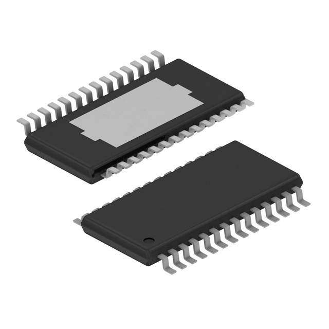
| 供应商器件封装 | 28-HTSSOP |
| 其它名称 | 296-23636-1 |
| 包装 | 剪切带 (CT) |
| 单位重量 | 118.500 mg |
| 压摆率 | - |
| 商标 | Texas Instruments |
| 安装类型 | 表面贴装 |
| 安装风格 | SMD/SMT |
| 封装 | Reel |
| 封装/外壳 | 28-SOIC(0.173",4.40mm 宽)裸露焊盘 |
| 封装/箱体 | HTSSOP-28 |
| 工作温度范围 | - 40 C to + 85 C |
| 工厂包装数量 | 2000 |
| 应用 | TFT-LCD 面板:伽玛缓冲器,VCOM 驱动器 |
| 最大工作温度 | + 85 C |
| 最小工作温度 | - 40 C |
| 标准包装 | 1 |
| 电压-电源,单/双 (±) | 9 V ~ 20 V |
| 电流-电源 | 12mA |
| 电流-输出/通道 | 30mA |
| 电源电流 | 115 uA, 12 mA |
| 电路数 | 18 |
| 系列 | BUF16821 |
| 输出类型 | 满摆幅 |


- 商务部:美国ITC正式对集成电路等产品启动337调查
- 曝三星4nm工艺存在良率问题 高通将骁龙8 Gen1或转产台积电
- 太阳诱电将投资9.5亿元在常州建新厂生产MLCC 预计2023年完工
- 英特尔发布欧洲新工厂建设计划 深化IDM 2.0 战略
- 台积电先进制程称霸业界 有大客户加持明年业绩稳了
- 达到5530亿美元!SIA预计今年全球半导体销售额将创下新高
- 英特尔拟将自动驾驶子公司Mobileye上市 估值或超500亿美元
- 三星加码芯片和SET,合并消费电子和移动部门,撤换高东真等 CEO
- 三星电子宣布重大人事变动 还合并消费电子和移动部门
- 海关总署:前11个月进口集成电路产品价值2.52万亿元 增长14.8%


PDF Datasheet 数据手册内容提取
BUF16821 BUF16821 www.ti.com SBOS428C–JULY2008–REVISEDJULY2011 Programmable Gamma-Voltage Generator and V Calibrator with Integrated Two-Bank Memory COM CheckforSamples:BUF16821 FEATURES DESCRIPTION 1 • 10-BITRESOLUTION The BUF16821 offers 16 programmable gamma 234 channelsandtwoprogrammableV channels. • 16-CHANNELP-GAMMA COM • 2-CHANNELP-V The final gamma and V values can be stored in COM COM • 16xREWRITABLENONVOLATILEMEMORY the on-chip, nonvolatile memory. To allow for programming errors or liquid crystal display (LCD) • TWOINDEPENDENTPIN-SELECTABLE panel rework, the BUF16821 supports up to 16 write MEMORYBANKS operationstotheon-chipmemory. • RAIL-TO-RAILOUTPUT The BUF16821 has two separate memory banks, – 300mVMinSwing-to-Rail(10mA) allowingsimultaneousstorageoftwodifferentgamma – > 300mAMaxI OUT curvestofacilitateswitchingbetweengammacurves. • LOWSUPPLYCURRENT All gamma and V channels offer a rail-to-rail • SUPPLYVOLTAGE:9Vto20V COM output that typically swings to within 150mV of either • DIGITALSUPPLY:2Vto5.5V supply rail with a 10mA load. All channels are • I2C™INTERFACE:Supports400kHzand programmed using an I2C interface that supports 3.4MHz standard operations up to 400kHz and high-speed datatransfersupto3.4MHz. APPLICATIONS The BUF16821 is manufactured using Texas • TFT-LCDREFERENCEDRIVERS Instruments’ proprietary, state-of-the-art, high-voltage CMOS process. This process offers very dense logic Digital Analog and high supply voltage operation of up to 20V. The BKSEL (2.0V to 5.5V) (9V to 20V) BUF16821 is offered in a HTSSOP-28 PowerPAD™ package,andisspecifiedfrom–40°Cto+85°C. 1 RELATEDPRODUCTS OUT1 FEATURES PRODUCT OUT2 22-ChannelGammaCorrectionBuffer BUF22821 16x Nonvolatile Memory BANK0 ¼16x Nonvolatile Memory BANK1 ¼DAC Registers ¼DAC Registers ¼ ¼ OOUUTT1156 111P1228882ro---VVC//g22SSrh00aauu--mCCnppmnpphhellaayyalnn,,bGnnTTleeearraallmVPPddCmiirrttOooiiaooMggnnrrCDaaaaollmmrirGGvrmmeeaarcaammtbbiommlleenaaBBBBBuuuuuffffffffeeeffeerrr,rrwss1i0th-BMit,eVmCoOryM BBBBBBUUUUUUFFFFFF122011200111888977002000000045 VCOM1 VCOM2 SDA SCL Control IF BUF16821 A0 1 Pleasebeawarethatanimportantnoticeconcerningavailability,standardwarranty,anduseincriticalapplicationsofTexas Instrumentssemiconductorproductsanddisclaimerstheretoappearsattheendofthisdatasheet. PowerPADisatrademarkofTexasInstruments. 2I2CisatrademarkofNXPSemiconductors. 3 Allothertrademarksarethepropertyoftheirrespectiveowners. 4 PRODUCTIONDATAinformationiscurrentasofpublicationdate. Copyright©2008–2011,TexasInstrumentsIncorporated Products conform to specifications per the terms of the Texas Instruments standard warranty. Production processing does not necessarilyincludetestingofallparameters.
BUF16821 SBOS428C–JULY2008–REVISEDJULY2011 www.ti.com This integrated circuit can be damaged by ESD. Texas Instruments recommends that all integrated circuits be handled with appropriateprecautions.Failuretoobserveproperhandlingandinstallationprocedurescancausedamage. ESDdamagecanrangefromsubtleperformancedegradationtocompletedevicefailure.Precisionintegratedcircuitsmaybemore susceptibletodamagebecauseverysmallparametricchangescouldcausethedevicenottomeetitspublishedspecifications. PACKAGE/ORDERINGINFORMATION(1) PRODUCT PACKAGE PACKAGEDESIGNATOR PACKAGEMARKING BUF16821A HTSSOP-28 PWP BUF16821 BUF16821B HTSSOP-28 PWP BUF16821B (1) ForthemostcurrentpackageandorderinginformationseethePackageOptionAddendumattheendofthisdocument,orseetheTI websiteatwww.ti.com. ABSOLUTE MAXIMUM RATINGS(1) Overoperatingfree-airtemperaturerange(unlessotherwisenoted). PARAMETER BUF16821 UNIT SupplyVoltage V +22 V S SupplyVoltage V +6 V SD DigitalInputPins,SCL,SDA,AO,BKSEL:Voltage –0.5to+6 V DigitalInputPins,SCL,SDA,AO,BKSEL:Current ±10 mA OutputPins,OUT1throughOUT16,V 1andV 2(2) (V–)–0.5to(V+)+0.5 V COM COM OutputShort-Circuit(3) Continuous AmbientOperatingTemperature –40to+95 °C AmbientStorageTemperature –65to+150 °C JunctionTemperature T +125 °C J HumanBodyModel (HBM) 3000 V ESDRating ChargedDeviceModel (CDM) 1000 V MachineModel (MM) 200 V (1) Stressesabovetheseratingsmaycausepermanentdamage.Exposuretoabsolutemaximumconditionsforextendedperiodsmay degradedevicereliability.Thesearestressratingsonly,andfunctionaloperationofthedeviceattheseoranyotherconditionsbeyond thosespecifiedisnotsupported. (2) SeetheOutputProtectionsection. (3) Short-circuittoground,oneamplifierperpackage. 2 Copyright©2008–2011,TexasInstrumentsIncorporated
BUF16821 www.ti.com SBOS428C–JULY2008–REVISEDJULY2011 ELECTRICAL CHARACTERISTICS Boldfacelimitsapplyoverthespecifiedtemperaturerange,T =–40°Cto+85°C. A AtT =+25°C,V =+18V,V =+2V,R =1.5kΩconnectedtoground,andC =200pF,unlessotherwisenoted. A S SD L L BUF16821 PARAMETER CONDITIONS MIN TYP MAX UNIT ANALOGGAMMABUFFERCHANNELS ResetValue Code512 9 V OUT1–16OutputSwing:High Code=1023,Sourcing10mA 17.7 17.85 V OUT1–16OutputSwing:Low Code=0,Sinking10mA 0.07 0.3 V VCOM1,2OutputSwing:High BUF16821A Code=1023,Sourcing100mA 13 16.2 V BUF16821B(1) Code=511,Sourcing100mA 8.96 V VCOM1,2OutputSwing:Low BUF16821A Code=0,Sinking100mA 0.6 2 V BUF16821B(1) Code=384,Sinking100mA 6.75 V ContinuousOutputCurrent Note(2) 30 mA OutputAccuracy ±20 ±50 mV vsTemperature Code512 ±25 μV/°C IntegralNonlinearity INL 0.3 LSB DifferentialNonlinearity DNL 0.3 LSB LoadRegulation,10mA REG Code512orVCC/2,IOUT=+5mAto–5mAStep 0.5 1.5 mV/mA OTPMEMORY NumberofOTPWriteCycles 16 Cycles MemoryRetention 100 Years ANALOGPOWERSUPPLY OperatingRange 9 20 V TotalAnalogSupplyCurrent IS OutputsatResetValues,NoLoad 12 14 mA OverTemperature 18 mA DIGITAL Logic1InputVoltage VIH 0.7×VSD V Logic0InputVoltage VIL 0.3×VSD V Logic0OutputVoltage VOL ISINK=3mA 0.15 0.4 V InputLeakage ±0.01 ±10 μA ClockFrequency fCLK Standard/FastMode 400 kHz High-SpeedMode 3.4 MHz DIGITALPOWERSUPPLY OperatingRange VSD 2.0 5.5 V DigitalSupplyCurrent(2) ISD OutputsatResetValues,NoLoad,Two-WireBusInactive 115 150 μA OverTemperature 115 μA TEMPERATURERANGE SpecifiedRange –40 +85 °C OperatingRange JunctionTemperature<+125°C –40 +95 °C StorageRange –65 +150 °C ThermalResistance(2) θJA HTSSOP-28 SeeNote(3) 40 °C/W (1) BUF16821Boutputswingislimitedinternally.Bits9,8,and7arefixedat'011'. (2) Observemaximumpowerdissipation. (3) Thermalpadattachedtoprintedcircuitboard(PCB),0lfmairflow,and76mm×76mmcopperarea. Copyright©2008–2011,TexasInstrumentsIncorporated 3
BUF16821 SBOS428C–JULY2008–REVISEDJULY2011 www.ti.com PIN CONFIGURATION PWPPACKAGE HTSSOP-28 (TOPVIEW) V 2 1 28 V 1 COM COM OUT1 2 27 OUT16 OUT2 3 26 OUT15 OUT3 4 25 OUT14 (1) OUT4 5 24 GND PowerPAD A Lead-Frame OUT5 6 23 V Die Pad S OUT6 7 Exposed on 22 OUT13 Underside (1) GND 8 (must connect to 21 OUT12 A GND and GND ) V 9 A D 20 OUT11 S OUT7 10 19 OUT10 (1) OUT8 11 18 GND D OUT9 12 17 BKSEL V 13 16 A0 SD SCL 14 15 SDA NOTE:(1)GND andGND mustbeconnectedtogether. A D 4 Copyright©2008–2011,TexasInstrumentsIncorporated
BUF16821 www.ti.com SBOS428C–JULY2008–REVISEDJULY2011 PINDESCRIPTIONS PIN# NAME DESCRIPTION 1 V 2 V channel2 COM COM 2 OUT1 DACoutput1 3 OUT2 DACoutput2 4 OUT3 DACoutput3 5 OUT4 DACoutput4 6 OUT5 DACoutput5 7 OUT6 DACoutput6 8 GND Analogground;mustbeconnectedtodigitalground(GND ). A D 9 V V connectedtoanalogsupply S S 10 OUT7 DACoutput7 11 OUT8 DACoutput8 12 OUT9 DACoutput9 13 V Digitalsupply;connecttologicsupply SD 14 SCL Serialclockinput;open-drain,connecttopull-upresistor. 15 SDA SerialdataI/O;open-drain,connecttopull-upresistor. 16 A0 A0addresspinforI2Caddress;connecttoeitherlogic1orlogic0.SeeTable1. 17 BKSEL Selectsmemorybank0or1;connecttoeitherlogic1toselectbank1orlogic0toselectbank0. 18 GND Digitalground;mustbeconnectedtoanaloggroundattheBUF16821. D 19 OUT10 DACoutput10 20 OUT11 DACoutput11 21 OUT12 DACoutput12 22 OUT13 DACoutput13 23 V V connectedtoanalogsupply S S 24 GND Analogground;mustbeconnectedtodigitalground(GND ). A D 25 OUT14 DACoutput14 26 OUT15 DACoutput15 27 OUT16 DACoutput16 28 V 1 V channel1 COM COM Copyright©2008–2011,TexasInstrumentsIncorporated 5
BUF16821 SBOS428C–JULY2008–REVISEDJULY2011 www.ti.com TYPICAL CHARACTERISTICS AtT =+25°C,V =+18V,V =+2V,R =1.5kΩconnectedtoground,andC =200pF,unlessotherwisenoted. A S SD L L OUTPUTVOLTAGEvsOUTPUTCURRENT OUTPUTVOLTAGEvsOUTPUTCURRENT (V 1andV 2) (Channels1–16) COM COM 18.0 18.0 17.5 17.5 17.0 17.0 16.5 V 1 16.5 COM V) 16.0 V) 16.0 Output Swing High e ( 15.5 e ( 15.5 g g olta 15.0 olta 15.0 put V 32..05 put V 32..05 Out 2.0 Out 2.0 1.5 1.5 1.0 VCOM2 1.0 Output Swing Low 0.5 0.5 0 0 0 25 50 75 100 125 150 0 25 50 75 100 125 150 Output Current (mA) Output Current (mA) Figure1. Figure2. DIGITALSUPPLYCURRENTvsTEMPERATURE ANALOGSUPPLYCURRENTvsTEMPERATURE 120 11.0 118 10.5 mA) 116 mA) 10.0 ent ( 114 ent ( 9.5 Curr 112 Curr 9.0 y 110 y pl pl 8.5 up 108 up Digital S 110064 Analog S 87..05 102 7.0 100 6.5 -50 -25 0 25 50 75 100 125 -50 -25 0 25 50 75 100 125 Temperature (°C) Temperature (°C) Figure3. Figure4. OUTPUTVOLTAGEvsTEMPERATURE DIFFERENTIALLINEARITYERROR 9.020 0.15 10 Typical Units Shown 9.015 0.10 9.010 V) 0.05 e ( 9.005 B) g S Volta 9.000 or (L 0 nitial 8.995 Err -0.05 I 8.990 -0.10 8.985 8.980 -0.15 -50 -25 0 25 50 75 100 125 0 256 512 768 1024 Temperature (°C) Input Code Figure5. Figure6. 6 Copyright©2008–2011,TexasInstrumentsIncorporated
BUF16821 www.ti.com SBOS428C–JULY2008–REVISEDJULY2011 TYPICAL CHARACTERISTICS (continued) AtT =+25°C,V =+18V,V =+2V,R =1.5kΩconnectedtoground,andC =200pF,unlessotherwisenoted. A S SD L L INTEGRALLINEARITYERROR BKSELSWITCHINGTIMEDELAY 0.15 0.10 BKSEL(2V/div) 0.05 B) LS 780ms or ( 0 Err 9V -0.05 DAC Channel (2V/div) -0.10 5V -0.15 0 256 512 768 1024 1ms/div Input Code Figure7. Figure8. LARGE-SIGNALSTEPRESPONSE v) di V/ 2 e ( g a olt V ut p ut O Time (2ms/div) Figure9. Copyright©2008–2011,TexasInstrumentsIncorporated 7
BUF16821 SBOS428C–JULY2008–REVISEDJULY2011 www.ti.com APPLICATION INFORMATION GENERAL All slaves on the bus shift in the slave address byte on the rising edge of SCL, with the last bit indicating The BUF16821 programmable voltage reference whether a read or write operation is intended. During allows fast and easy adjustment of 16 programmable the ninth clock pulse, the slave being addressed gamma reference outputs and two V outputs, COM responds to the master by generating an each with 10-bit resolution. The BUF16821 is AcknowledgeandpullingSDALOW. programmed through a high-speed, I2C interface. The final gamma and V values can be stored in the Data transfer is then initiated and eight bits of data COM onboard, nonvolatile memory. To allow for are sent, followed by an Acknowledge bit. During programming errors or liquid crystal display (LCD) data transfer, SDA must remain stable while SCL is panel rework, the BUF16821 supports up to 16 write HIGH. Any change in SDA while SCL is HIGH is operations to the onboard memory. The BUF16821 interpretedasaSTARTorSTOPcondition. has two separate memory banks, allowing Once all data have been transferred, the master simultaneous storage of two different gamma curves generates a STOP condition, indicated by pulling to facilitate dynamic switching between gamma SDA from LOW to HIGH while SCL is HIGH. The curves. BUF16821 can act only as a slave device; therefore, The BUF16821 can be powered using an analog it never drives SCL. SCL is an input only for the supply voltage from 9V to 20V, and a digital supply BUF16821. from 2V to 5.5V. The digital supply must be applied before the analog supply to avoid excessive current ADDRESSING THE BUF16821 and power consumption, or possibly even damage to The address of the BUF16821 is 111010x, where x is the device if left connected only to the analog supply the state of the A0 pin. When the A0 pin is LOW, the for extended periods of time. Figure 10 illustrates a device acknowledges on address 74h (1110100). If typicalconfigurationoftheBUF16821. the A0 pin is HIGH, the device acknowledges on address 75h (1110101). Table 1 shows the A0 pin TWO-WIRE BUS OVERVIEW settingsandBUF16821addressoptions. The BUF16821 communicates over an Other valid addresses are possible through a simple industry-standard, two-wire interface to receive data mask change. Contact your TI representative for in slave mode. This standard uses a two-wire, information. open-drain interface that supports multiple devices on a single bus. Bus lines are driven to a logic low level Table1.Quick-ReferenceofBUF16821Addresses only. The device that initiates the communication is called a master, and the devices controlled by the DEVICE/COMPONENT master are slaves. The master generates the serial BUF16821Address ADDRESS clock on the clock signal line (SCL), controls the bus A0pinisLOW access, and generates the START and STOP 1110100 (deviceacknowledgesonaddress74h) conditions. A0pinisHIGH 1110101 To address a specific device, the master initiates a (deviceacknowledgesonaddress75h) START condition by pulling the data signal line (SDA) from a HIGH to a LOW logic level while SCL is HIGH. Table2.Quick-ReferenceofCommandCodes COMMAND CODE General-CallReset Addressbyteof00hfollowedbyadatabyteof06h. High-SpeedMode 00001xxx,withSCL≤400kHz;wherexxxarebitsuniquetotheHs-capablemaster.This byteiscalledtheHsmastercode. 8 Copyright©2008–2011,TexasInstrumentsIncorporated
BUF16821 www.ti.com SBOS428C–JULY2008–REVISEDJULY2011 BUF16821 (1) (1) VCOM2 1 VCOM2 VCOM1 28 VCOM1 (1) (1) 2 OUT1 OUT16 27 (1) (1) Source 3 OUT2 OUT15 26 Driver (1) (1) 4 OUT3 OUT14 25 Source Driver (1) 5 OUT4 GND (2) 24 A (1) 6 OUT5 VS 23 100nF 10mF VS (1) (1) 7 OUT6 OUT13 22 (2) (1) 8 GNDA OUT12 21 Source Driver (1) VS 9 VS OUT11 20 100nF 10mF (1) (1) 10 OUT7 OUT10 19 Source (1) 11 OUT8 GND (2) 18 Driver D (1) 12 OUT9 BKSEL 17 3.3V 13 VSD A0 16 1mF 100nF 14 SSCCLL SDA 15 Timing Controller (1) RCcombinationoptional;seetheOutputProtectionsection. (2) GND andGND mustbeconnectedtogether. A D Figure10. TypicalApplicationConfiguration Copyright©2008–2011,TexasInstrumentsIncorporated 9
BUF16821 SBOS428C–JULY2008–REVISEDJULY2011 www.ti.com DATA RATES OUTPUT VOLTAGE The two-wire bus operates in one of three speed Buffer output values are determined by the analog modes: supply voltage (V ) and the decimal value of the S • Standard: allows a clock frequency of up to binary input code used to program that buffer. The 100kHz; valueiscalculatedusingEquation1: • Fast: allows a clock frequency of up to 400kHz; V = V ´ CODE10 and OUT S 1024 (1) • High-speed mode (also called Hs mode): allows a clockfrequencyofupto3.4MHz. The BUF16821 outputs are capable of a full-scale voltage output change in typically 5μs; no The BUF16821 is fully compatible with all three intermediatestepsarerequired. modes. No special action is required to use the device in Standard or Fast modes, but High-speed UPDATING THE DAC OUTPUT VOLTAGES mode must be activated. To activate High-speed mode,sendaspecialaddressbyteof00001xxx,with Because the BUF16821 features a double-buffered SCL ≤ 400kHz, following the START condition; where register structure, updating the digital-to-analog xxx are bits unique to the Hs-capable master, which converter (DAC) and/or the V register is not the COM can be any value. This byte is called the Hs master same as updating the DAC and/or V output COM code. Table 2 provides a reference for the voltage. There are two methods for updating the High-speed mode command code. (Note that this DAC/V outputvoltages. COM configuration is different from normal address Method 1: Method 1 is used when it is desirable to bytes—the low bit does not indicate read/write have the DAC/V output voltage change status.) The BUF16821 responds to the High-speed COM immediately after writing to a DAC register. For each command regardless of the value of these last three write transaction, the master sets data bit 15 to a '1'. bits. The BUF16821 does not acknowledge this byte; The DAC/V output voltage update occurs after the communication protocol prohibits COM receiving the 16th data bit for the currently-written acknowledgment of the Hs master code. Upon register. receiving a master code, the BUF16821 switches on its Hs mode filters, and communicates at up to Method 2: Method 2 is used when it is desirable to 3.4MHz. Additional high-speed transfers may be have all DAC/V output voltages change at the COM initiated without resending the Hs mode byte by same time. First, the master writes to the desired generating a repeat START without a STOP. The DAC/V channels with data bit 15 a '0'. Then, COM BUF16821 switches out of Hs mode with the next when writing the last desired DAC/V channel, the COM STOPcondition. master sets data bit 15 to a '1'. All DAC/V COM channels are updated at the same time after GENERAL-CALL RESET AND POWER-UP receivingthe16thdatabit. The BUF16821 responds to a General-Call Reset, NONVOLATILE MEMORY which is an address byte of 00h (0000 0000) followed by a data byte of 06h (0000 0110). The BUF16821 BKSELPin acknowledges both bytes. Table 2 provides a reference for the General-Call Reset command code. The BUF16821 has 16x rewrite capability of the Upon receiving a General-Call Reset, the BUF16821 nonvolatile memory. Additionally, the BUF16821 has performs a full internal reset, as though it had been the ability to store two distinct gamma curves in two powered off and then on. It always acknowledges the different nonvolatile memory banks, each of which General-Call address byte of 00h (0000 0000), but has 16x rewrite capability. One of the two available does not acknowledge any General-Call data bytes banks is selected using the external input pin, otherthan06h(00000110). BKSEL. When this pin is low, BANK0 is selected; whenthispinishigh,BANK1isselected. When the BUF16821 powers up, it automatically performs a reset. As part of the reset, the BUF16821 is configured for all outputs to change to the last programmed nonvolatile memory values, or 1000000000 if the nonvolatile memory values have notbeenprogrammed. 10 Copyright©2008–2011,TexasInstrumentsIncorporated
BUF16821 www.ti.com SBOS428C–JULY2008–REVISEDJULY2011 When the BKSEL pin changes state, the BUF16821 Single-ChannelAcquireCommand acquires the last programmed DAC/V values from COM These are the steps to initiate a single-channel the nonvolatile memory associated with this newly acquire: chosen bank. At power-up, the state of the BKSEL pindetermineswhichmemorybankisselected. 1. Be sure BKSEL is in its desired state and has beenstableforatleast1ms. The I2C master also has the ability to update 2. SendaSTARTconditiononthebus. (acquire) the DAC registers with the last programmed nonvolatile memory values using software control. 3. Send the device address (based on A0) and The bank to be acquired depends on the state of read/write bit = LOW. The BUF16821 BKSEL. acknowledgesthisbyte. 4. Send a DAC/V pointer address byte using the COM GeneralAcquireCommand DAC/V address corresponding to the output COM and register to update with the OTP memory A general acquire command is used to update all value. Set bit D7 = 0 and D6 = 1. Bits D5–D0 are registers and DAC/V outputs to the last COM the DAC/V address. Although the BUF16821 programmed values stored in nonvolatile memory. A COM acknowledges 000000 through 010111, it stores single-channel acquire command updates only the andreturnsdataonlyfromtheseaddresses: register and DAC/V output of the DAC/V COM COM corresponding to the DAC/V address used in the – 000000through001111 COM single-channelacquirecommand. – 010010and010011 It returns 0000 reads from 010000 and 010001, These are the steps of the sequence to initiate a and 010100 through 010111. See Table 4 for generalchannelacquire: validDAC/V addresses. COM 1. Be sure BKSEL is in its desired state and has 5. SendaSTOPconditiononthebus. beenstableforatleast1ms. Approximately 36μs (±4μs) after issuing this 2. SendaSTARTconditiononthebus. command, the specified DAC/V register and 3. Send the appropriate device address (based on COM DAC/V output voltage change to the appropriate A0) and the read/write bit = LOW. The BUF16821 COM OTPmemoryvalue. acknowledgesthisbyte. 4. Send a DAC/VCOM pointer address byte. Set bit MaxBank D7 = 1 and D6 = 0. Bits D5–D0 are any valid The BUF16821 can provide the user with the number DAC/V address. Although the BUF16821 COM of times the nonvolatile memory of a particular acknowledges 000000 through 010111, it stores DAC/V channel nonvolatile memory has been andreturnsdataonlyfromtheseaddresses: COM written to for the current memory bank. This – 000000through001111 information is provided by reading the register at – 010010and010011 pointeraddress111111. It returns 0000 for reads from 010000 and 010001, and 010100 through 010111. See TherearetwowaystoupdatetheMaxBankregister: Table4forvalidDAC/V addresses. 1. After initiating a single acquire command, the COM 5. SendaSTOPconditiononthebus. BUF16821 updates the MaxBank register with a code corresponding to how many times that Approximately 750μs (±80μs) after issuing this particularchannelmemoryhasbeenwrittento. command, all DAC/V registers and DAC/V COM COM 2. Following a general acquire command, the output voltages change to the respective, appropriate BUF16821 updates the MaxBank register with a nonvolatilememoryvalues. code corresponding to the maximum number of xxx times the most used channel (OUT1–16 and V s)hasbeenwrittento. xxx COM MaxBank is a read-only register and is only updated byperformingageneral-orsingle-channelacquire. Copyright©2008–2011,TexasInstrumentsIncorporated 11
BUF16821 SBOS428C–JULY2008–REVISEDJULY2011 www.ti.com Table 3 shows the relationship between the number READ/WRITE OPERATIONS of times the nonvolatile memory has been Read and write operations can be done for a single programmed and the corresponding state of the DAC/V or for multiple DACs/V s. Writing to a MaxBankRegister. COM COM DAC/V register differs from writing to the COM nonvolatile memory. Bits D15–D14 of the most Table3.MaxBankDetails significant byte of data determines if data are written NUMBEROFTIMESWRITTENTO RETURNSCODE totheDAC/V registerorthenonvolatilememory. COM 0 0000 Read/Write:DAC/V Register(volatilememory) 1 0000 COM 2 0001 The BUF16821 is able to read from a single 3 0010 DAC/V , or multiple DACs/V s, or write to the COM COM 4 0011 register of a single DAC/V , or multiple COM 5 0100 DACs/VCOMs in a single communication transaction. DAC pointer addresses begin with 000000 (which 6 0101 corresponds to OUT1) through 001111 (which 7 0110 corresponds to OUT16). Addresses 010010 and 8 0111 010011areV 1andV 2,respectively. 9 1000 COM COM 10 1001 Write commands are performed by setting the read/write bit LOW. Setting the read/write bit HIGH 11 1010 performsareadtransaction. 12 1011 13 1100 Writing:DAC/V Register(VolatileMemory) 14 1101 COM 15 1110 TowritetoasingleDAC/VCOMregister: 16 1111 1. SendaSTARTconditiononthebus. 2. Send the device address and read/write bit = ParityErrorCorrection LOW.TheBUF16821acknowledgesthisbyte. The BUF16821 provides single-bit parity error 3. Send a DAC/VCOM pointer address byte. Set bit correction for data stored in the nonvolatile memory D7 = 0 and D6 = 0. Bits D5–D0 are the to provide increased reliability of the nonvolatile DAC/VCOM address. Although the BUF16821 memory. If a single bit of nonvolatile memory for a acknowledges 000000 through 010111, it stores channel fails, the BUF16821 corrects for it and andreturnsdataonlyfromtheseaddresses: updates the appropriate DAC with the intended value – 000000through001111 whenitsmemoryisacquired. – 010010through010011 If more than one bit of nonvolatile memory for a It returns 0000 for reads from 010000 through channel fails, the BUF16821 does not correct for it, 010001, and 010100 through 010111. See and updates the appropriate DAC/VCOM with the Table4forvalidDAC/VCOMaddresses. defaultvalueof1000000000. 4. Send two bytes of data for the specified register. Begin by sending the most significant byte first DIE_ID AND DIE_REV REGISTERS (bits D15–D8, of which only bits D9 and D8 are used, and bits D15–D14 must not be 01), The user can verify the presence of the BUF16821 in followed by the least significant byte (bits the system by reading from address 111101. When D7–D0). The register is updated after receiving read at this address, the BUF16821A returns thesecondbyte. 0101100100100111 and the BUF16821B returns 5. SendaSTOPorSTARTconditiononthebus. 0101100100100100. The user can also determine the die revision of the BUF16821 by reading from register 111100. BUF16821 returns 0000000000000000 when a RevA die is present. RevB would be designated by 0000000000000001andsoon. 12 Copyright©2008–2011,TexasInstrumentsIncorporated
BUF16821 www.ti.com SBOS428C–JULY2008–REVISEDJULY2011 The BUF16821 acknowledges each data byte. If the 5. SendaSTOPorSTARTconditiononthebus. master terminates communication early by sending a The BUF16821 acknowledges each byte. To STOP or START condition on the bus, the specified terminate communication, send a STOP or START register is not updated. Updating the DAC/V COM condition on the bus. Only DAC registers that have register is not the same as updating the DAC/V COM receivedbothbytesofdataareupdated. output voltage; see the Updating the DAC Outputs section. Reading:DAC/V /OTHERRegister(Volatile COM The process of updating multiple DAC/V registers Memory) COM begins the same as when updating a single register. Reading a register returns the data stored in that However, instead of sending a STOP condition after DAC/V /OTHERregister. writing the addressed register, the master continues COM to send data for the next register. The BUF16821 ToreadasingleDAC/V /OTHERregister: COM automatically and sequentially steps through 1. SendaSTARTconditiononthebus. subsequent registers as additional data are sent. The 2. Send the device address and read/write bit = process continues until all desired registers have LOW.TheBUF16821acknowledgesthisbyte. beenupdatedoraSTOPorSTARTconditionissent. 3. Send the DAC/V /OTHER pointer address COM TowritetomultipleDAC/VCOMregisters: byte. Set bit D7 = 0 and D6 = 0; bits D5–D0 are 1. SendaSTARTconditiononthebus. the DAC/V /OTHER address. NOTE: The COM 2. Send the device address and read/write bit = BUF16821 stores and returns data only from LOW.TheBUF16821acknowledgesthisbyte. theseaddresses: 3. Send either the OUT1 pointer address byte to – 000000through001111 start at the first DAC, or send the pointer address – 010010 byte for whichever DAC/VCOM is the first in the – 010011 sequence of DACs/V s to be updated. The COM – 111100through111111 BUF16821 begins with this DAC/V and steps COM It returns 0000 for reads from 010000 and through subsequent DACs/V s in sequential COM 010001, and 010100 through 010111. See order. Table4forvalidDAC/V /OTHERaddresses. COM 4. Send the bytes of data; begin by sending the 4. SendaSTARTorSTOP/STARTcondition. most significant byte (bits D15–D8, of which only 5. Send the correct device address and read/write bits D9 and D8 have meaning, and bits D15–D14 bit = HIGH. The BUF16821 acknowledges this must not be 01), followed by the least significant byte. byte (bits D7–D0). The first two bytes are for the DAC/V addressed in the previous step. The 6. Receive two bytes of data. They are for the COM DAC/V register is automatically updated after specified register. The most significant byte (bits COM receivingthesecondbyte.Thenexttwobytesare D15–D8) is received first; next is the least for the following DAC/V . That DAC/V significant byte (bits D7–D0). In the case of COM COM register is updated after receiving the fourth byte. DAC/V channels, bits D15–D10 have no COM This process continues until the registers of all meaning. following DACs/VCOMs have been updated. The 7. Acknowledgeafterreceivingthefirstbyte. BUF16821 continues to accept data for a total of 8. Send a STOP or START condition on the bus or 18 DACs; however, the two data sets following do not acknowledge the second byte to end the the 16th data set are meaningless. The 19th and readtransaction. 20th data sets apply to V 1 and V 2. The COM COM write disable bit cannot be accessed using this method. It must be written to using the write to a singleDACregisterprocedure. Copyright©2008–2011,TexasInstrumentsIncorporated 13
BUF16821 SBOS428C–JULY2008–REVISEDJULY2011 www.ti.com Communication may be terminated by sending a Towritetoasinglenonvolatileregister: premature STOP or START condition on the bus, or 1. SendaSTARTconditiononthebus. bynotacknowledging. 2. Send the device address and read/write bit = Toreadmultipleregisters: LOW. The BUF16821 acknowledges this byte. 1. SendaSTARTconditiononthebus. Although the BUF16821 acknowledges 000000 through 010111, it stores and returns data only 2. Send the device address and read/write bit = fromtheseaddresses: LOW.TheBUF16821acknowledgesthisbyte. – 000000through001111 3. Send either the OUT1 pointer address byte to – 010010and010011 start at the first DAC, or send the pointer address It returns 0000 for reads from 010000 through byte for whichever register is the first in the 010001, and 010100 through 010111. See sequence of DACs/V s to be read. The COM Table4forDAC/V addresses. BUF16821 begins with this DAC/V and steps COM COM through subsequent DACs/V s in sequential 3. Send a DAC/V pointer address byte. Set bit COM COM order. D7 = 0 and D6 = 0. Bits D5–D0 are the DAC/V address. 4. Send a START or STOP/START condition on the COM bus. 4. Sendtwobytesofdataforthenonvolatileregister of the specified DAC/V . Begin by sending the 5. Send the correct device address and read/write COM most significant byte first (bits D15–D8, of which bit = HIGH. The BUF16821 acknowledges this only bits D9 and D8 are data bits, and bits byte. D15–D14 must be 01), followed by the least 6. Receive two bytes of data. They are for the significant byte (bits D7–D0). The register is specified DAC/V . The first received byte is the COM updatedafterreceivingthesecondbyte. most significant byte (bits D15–D8; only bits D9 5. SendaSTOPconditiononthebus. and D8 have meaning), next is the least significantbyte(bitsD7–D0). The BUF16821 acknowledges each data byte. If the 7. Acknowledgeafterreceivingeachbyteofdata. master terminates communication early by sending a STOP or START condition on the bus, the specified 8. When all desired DACs have been read, send a nonvolatile register is not updated. Writing a STOPorSTARTconditiononthebus. nonvolatile register also updates the DAC/V COM Communication may be terminated by sending a registerandoutputvoltage. premature STOP or START condition on the bus, or The DAC/V register and DAC/V output voltage by not sending the acknowledge bit. The reading of COM COM are updated immediately, while the programming of registers DieID, DieRev, and MaxBank is not the nonvolatile memory takes up to 250μs. Once a supported in this mode of operation (these values nonvolatile register write command has been issued, mustbereadusingthesingleregisterreadmethod). no communication with the BUF16821 should take place for at least 250μs. Writing or reading over the Write:NonvolatileMemoryfortheDACRegister serial interface while the nonvolatile memory is being The BUF16821 is able to write to the nonvolatile written jeopardizes the integrity of the data being memory of a single DAC/VCOM in a single stored. communication transaction. In contrast to the BUF20820, writing to multiple nonvolatile memory Read:NonvolatileMemoryfortheDACRegister words in a single transaction is not supported. Valid To read the data present in nonvolatile register for a DAC/V pointer addresses begin with 000000 COM particular DAC/V channel, the master must first (which corresponds to OUT1) through 001111 (which COM issue a general acquire command, or a single acquire corresponds to OUT16). Addresses 010010 and command with the appropriate DAC/V channel 010011areV 1andV 2,respectively. COM COM COM chosen. This action updates both the DAC/V COM When programming the nonvolatile memory, the register(s) and DAC/V output voltage(s). The COM analog supply voltage must be between 9V and 20V. master may then read from the appropriate Write commands are performed by setting the DAC/V registerasdescribedearlier. COM read/writebitLOW. 14 Copyright©2008–2011,TexasInstrumentsIncorporated
BUF16821 www.ti.com SBOS428C–JULY2008–REVISEDJULY2011 Table4.DACRegisterPointerAddresses DACREGISTER POINTERADDRESS OUT1 000000 OUT2 000001 OUT3 000010 OUT4 000011 OUT5 000100 OUT6 000101 OUT7 000110 OUT8 000111 OUT9 001000 OUT10 001001 OUT11 001010 OUT12 001011 OUT13 001100 OUT14 001101 OUT15 001110 OUT16 001111 VCOM1 010010 VCOM2 010011 OTHERREGISTER POINTERADDRESS Die_Rev 111100 Die_ID 111101 MaxBank 111111 Copyright©2008–2011,TexasInstrumentsIncorporated 15
BUF16821 SBOS428C–JULY2008–REVISEDJULY2011 www.ti.com DAC LSDAC MSbyte. byteD14 must be 0.StopAcknAcknAckn D10D13D15P0D6D8D9D0D3D5AcknAcknAcknD11D12D14D7D1D2D4 D13D15P0D9D10D3D5D6D8D0AcknAcknAcknD12D14D11D7D1D2D4 If D15 = 1, all DACs are updated when the current DAC register is updated. The entire DAC register D9-D0is updated at this moment. DAC DDAC (pointer) L(pointer) MSbyte. AC (pointer + 1) MSbyteD14 must be 0.Sbyte. D14 must be 0.AcknAcknAckn D15D13D10D13D15P0DDD6D8D9D035AcknAcknAcknD14D1D12D14D71D1D2D4 D10D13D15P0DDDD6D8D90D15D1335AAAcknckncknDDD111214D7D14D1D2D4 If D15 = 1, all DACs are updated when the current DAC register is updated. The entire DAC register D9-D0is updated at this moment. DAC 20 (VOUT2) MSbyte. D14 must be 0.DAC 20 LSbyteStopAckAcknnCOM D10D13D15DDD6D8D9D035AcknAcknD11D12D14D2D4D7D1 DD13D15D6D8D910D0D3D5AckAcknnD12D14D11D2D4D7D1 NoAcknDAC MSbyte. D15-D10 have no meDAC LSbyte.aning.StopDevice AddressReadAcknAckn A3A5A6D10D13D15A0DDD6D8D9D035AcknAcknA1A2A4D11D12D14RD2D4D7D1 A3A5A6A0D10D13D15D3D5D6D8D9D0AcknAcknNo AcknA1A2A4D1D1RD1124D2D4D7D1 DAC (pointer) MSbyte. D15-D10 have no meaning.Device AddressReadAcknAckn A6DD13D15A0A3A5D8D910AcknAcknA2A4D11D12D14RA1 A6A0A3A5D10D13D15D8D9AcknAcknA1A2A4D1D12D14R1 DAC 20 (VOUT2) MSbyte. D15-D10 have no meaning.DAC 20 LSbyte.StopAcknAcknCOM D13D15D6D8D9D10D0D3D5AcknAcknD12D14D11D1D2D4D7 D1D1D9D1035DD3D5D6D80AcknAcknD11D12D14D2D4D7D1 Write OperationDAC address pointer. D7-D5 must be 000.Ackn P3D5D6AcknP2P4D7P1 D6P3D5AcknP2P4D7P1 Write OperationDAC address pointer. D7-D5 must be 000.Ackn P3D5D6AcknP2P4D7P1 P3D5D6AcknP2P4D7P1 DAC address pointer. D7-D5 must be 000.AcknStart D5D6P0P3AcknP2P4P1 D6P3D5P0AcknP1P2P4 Start DAC address pointer. D7-D5 must be 000.AcknStart D6PP3D50AcknP1P2P4 D6P3D5P0AcknPPP124 Write single DAC register. P4-P0 specify DAC address. StartWriteDevice Address SCL SDA_InA3A5A6A0A2A4WA1 Device_OutAA0A3A56A2A4WA1 Write multiple DAC registers. P4-P0 specify DAC address. WriteDevice AddressStart SCL SDA_InA3A5A6A0AAWA124 Device_OutA3A5A6A0AAWA124 Read single Read operatiDAC register. P4-P0 spon.ecify DAC address. Device AddressWriteAcknStart SCL SDA_InA0A3A5A6AcknA4D7WA1A2 Device_OutA0A3A5AcknA6A1A2A4D7W RRead multiple DAC regisead operation.ters. P4-P0 specify DAC address. Device AddressWriteAcknStart SCL SDA_InA0A3A5A6AcknD7WA1A2A4 Device_OutA0A3A5A6AcknD7WA1A2A4 Figure11. WriteDACRegisterTiming Figure12. ReadRegisterTiming 16 Copyright©2008–2011,TexasInstrumentsIncorporated
BUF16821 www.ti.com SBOS428C–JULY2008–REVISEDJULY2011 t1 t2 Write supply active.Write signal active.DAC LSbyte.StopAckn D0D3AcknD1D2D4 D0D3AcknD1D2D4 The OTP register (D9-D0) is updated at this moment.mt: > 20s before falling edge of clock.1mt: minimum 100s, maximum 2ms.2 D5 D5 Stop Stop D6D7 D6D7 Ackn Ackn Ackn Ackn Ackn Ackn P0 P0 P0 P0 Ackn Ackn Ackn P1 P1 P1 P1 DAC MSbyte. D15-D14 must be 01. D13D9D10D8D1D14D112 D13D8D9D10DD12D1411 DAC address pointer. D7-D5 must be 100. PD5D63P2P4 PD5D63P2P4 DAC address pointer. D7-D5 must be 010. DDP356P2P4 P3D5D6P2P4 Ackn D15Ackn D15Ackn Write Operation Ackn AcknD7 AcknD7 Write Operation Ackn AcknD7 AcknD7 Write operation.DAC address pointer. D7-D0 must be 000.WriteAckn DA0P3D56P0AcknD7WP4P1P2 D6A0P0P3D5AcknD7WP1P2P4 General acquire command. P4-P0 must specify and valid DAC address. Device address.WriteStart A0A3A5A6A1A2A4W A0A3A5A6AWA1A24 Single channel acquire command. P4-P0 must specify and valid DAC address. Device addresWrites.Start A0A3A5A6WA1A2A4 AA5A6A03WA1A2A4 Write single OTP register. P4-P0 specify DAC address. Device AddressStart A5A6A3A1A2A4 A3A5A6A4A1A2 SCL SDA_In Device_Out SCL SDA_In Device_Out SCL SDA_In Device_Out Figure13. WriteNonvolatileRegisterTiming Figure14. AcquireOperationTiming Copyright©2008–2011,TexasInstrumentsIncorporated 17
BUF16821 SBOS428C–JULY2008–REVISEDJULY2011 www.ti.com Address AcknByte = 06h evice begins reset at arrow and is in reset until ACK clock pulse.Then the device acquires memory, etc., as it does at power-up. No Ackn Device enters high-speed mode at ACK clock pulse.Device exits high-speed mode with stop condition. D Code) Ackn Master S H Byte = 00001xxx ( Address Byte = 00h Address General-Call Reset Command Start High-Speed Command Start L A C D L A S S C D S S Figure15. General-CallResetTiming Figure16. High-SpeedModeTiming 18 Copyright©2008–2011,TexasInstrumentsIncorporated
BUF16821 www.ti.com SBOS428C–JULY2008–REVISEDJULY2011 END-USER SELECTED GAMMA CONTROL DYNAMIC GAMMA CONTROL Because the BUF16821 has two banks of nonvolatile Dynamic gamma control is a technique used to memory, it is well-suited for providing two levels of improve the picture quality in LCD television gamma control by using the BKSEL pin, as shown in applications. This technique typically requires Figure17.WhenthestateoftheBKSELpinchanges, switching gamma curves between frames. Using the the BUF16821 updates all 18 programmable buffer BKSEL pin to switch between two gamma curves outputssimultaneouslyafter750μs(±80μs). does not often provide good results because of the 750μs required to transfer the data from the To update all 18 programmable output voltages nonvolatile memory to the DAC register. However, simultaneouslyviahardware,toggletheBKSELpinto dynamic gamma control can still be accomplished by switch between Gamma Curve 0 (stored in Bank0) storing two gamma curves in an external EEPROM andGammaCurve1(storedinBank1). andwritingdirectlytotheDACregister(volatile). All DAC/V registers and output voltages are COM The double register input structure saves updatedsimultaneouslyafterapproximately750μs. programmingtimebyallowingupdatedDACvaluesto be pre-stored into the first register bank. Storage of 5V this data can occur while a picture is still being displayed. Because the data are only stored into the BUF16821 first register bank, the DAC/V output values BKSEL COM remain unchanged—the display is unaffected. At the beginning or the end of a picture frame, the Switch OUT1 DAC/VCOM outputs (and therefore, the gamma voltages) can be quickly updated by writing a '1' in bit 15 of any DAC/V register. For details on the COM operation of the double register input structure, see theUpdatingtheDACOutputssection. Change in NK0 NK1 Output Voltages To update all 18 programmable output voltages A A B B simultaneously via software, perform the following actions: OUT16 STEP1:Writetoregisters1–18withbit15always'0'. STEP 2: Write any DAC/V register a second time COM with identical data. Make sure that bit 15 is set to '1'. I2C All DAC/V channels are updated simultaneously COM afterreceivingthelastbitofdata. Figure17. GammaControl Copyright©2008–2011,TexasInstrumentsIncorporated 19
BUF16821 SBOS428C–JULY2008–REVISEDJULY2011 www.ti.com OUTPUT PROTECTION exceeded. Protection against the high current flow may be provided by placing current-limiting resistors The BUF16821 output stages can safely source and in series with the output, as shown in Figure 10. sink the current levels indicated in Figure 1 and Select a resistor value that restricts the current level Figure 2. However, there are other modes where tothemaximumratingfortheparticularpin. precautions must be taken to prevent to the output stages from being damaged by excessive current flow. The outputs (OUT1 through OUT16, V 1 and VS COM V 2) include ESD protection diodes, as shown in COM Figure 18. Normally, these diodes do not conduct and ESD Current are passive during typical device operation. Unusual BUF16821 Steering Diodes operating conditions can occur where the diodes may conduct, potentially subjecting them to high, even damaging current levels. These conditions are most OUTX likely to occur when a voltage applied to an output or exceeds(V )+0.5V,ordropsbelowGND– 0.5V. V X S COM Onecommonscenariowherethisconditioncanoccur is when the output pin is connected to a sufficiently large capacitor, and the BUF16821 power-supply source (V ) is suddenly removed. Removing the S power-supply source allows the capacitor to discharge through the current-steering diodes. The energy released during the high current flow period Figure18. OutputPinsESDProtection causes the power dissipation limits of the diode to be Current-SteeringDiodes 20 Copyright©2008–2011,TexasInstrumentsIncorporated
BUF16821 www.ti.com SBOS428C–JULY2008–REVISEDJULY2011 GENERAL POWERPAD DESIGN examplethermallandpatternmechanicaldrawing CONSIDERATIONS isattachedtotheendofthisdatasheet. The BUF16821 is available in a thermally-enhanced 3. Additional vias may be placed anywhere along PowerPAD package. This package is constructed the thermal plane outside of the thermal pad area using a downset leadframe upon which the die is to help dissipate the heat generated by the mounted; see Figure 19(a) and Figure 19(b). This BUF16821 IC. These additional vias may be arrangement results in the lead frame being exposed larger than the 13-mil diameter vias directly under as a thermal pad on the underside of the package; the thermal pad. They can be larger because see Figure 19(c). This thermal pad has direct thermal they are not in the thermal pad area to be contact with the die; thus, excellent thermal soldered;thus,wickingisnotaproblem. performance is achieved by providing a good thermal 4. Connect all holes to the internal plane that is at pathawayfromthethermalpad. thesamevoltagepotentialastheGNDpins. The PowerPAD package allows for both assembly 5. When connecting these holes to the internal and thermal management in one manufacturing plane, do not use the typical web or spoke via operation. During the surface-mount solder operation connection methodology. Web connections have (when the leads are being soldered), the thermal pad a high thermal resistance connection that is must be soldered to a copper area underneath the useful for slowing the heat transfer during package. Through the use of thermal paths within this soldering operations. This configuration makes copper area, heat can be conducted away from the the soldering of vias that have plane connections package into either a ground plane or other easier. In this application, however, low thermal heat-dissipating device. Soldering the PowerPAD to resistance is desired for the most efficient heat the printed circuit board (PCB) is always required, transfer. Therefore, the holes under the even with applications that have low power BUF16821 PowerPAD package should make dissipation. This technique provides the necessary their connection to the internal plane with a thermal and mechanical connection between the lead complete connection around the entire framediepadandthePCB. circumferenceoftheplated-throughhole. 6. The top-side solder mask should leave the The PowerPAD must be connected to the most terminals of the package and the thermal pad negative supply voltage on the device, GND and A area with its twelve holes exposed. The GND . D bottom-side solder mask should cover the holes 1. Prepare the PCB with a top-side etch pattern. of the thermal pad area. This masking prevents There should be etching for the leads as well as solder from being pulled away from the thermal etchforthethermalpad. padareaduringthereflowprocess. 2. Place recommended holes in the area of the 7. Apply solder paste to the exposed thermal pad thermal pad. Ideal thermal land size and thermal areaandalloftheICterminals. via patterns for the HTSSOP-28 PWP package 8. With these preparatory steps in place, simply can be seen in the technical brief, PowerPAD place the BUF16821 IC in position and run the Thermally-Enhanced Package (SLMA002), chip through the solder reflow operation as any available for download at www.ti.com. These standard surface-mount component. This holes should be 13 mils (0,33mm) in diameter. preparationresultsinaproperlyinstalledpart. Keep them small, so that solder wicking through the holes is not a problem during reflow. An Copyright©2008–2011,TexasInstrumentsIncorporated 21
BUF16821 SBOS428C–JULY2008–REVISEDJULY2011 www.ti.com DIE Side View (a) Thermal Pad DIE End View (b) Bottom View (c) Figure19. ViewsofThermally-EnhancedPWPPackage For a given θ (listed in the Electrical JA Characteristics), the maximum power dissipation is 5.0 showninFigure20andcalculatedbyEquation2: 4.5 (T -T ) W) P = MAX A n ( 4.0 D qJA (2) patio 3.5 ssi 3.0 Where: Di er 2.5 w P =maximumpowerdissipation(W) o 2.0 D P m 1.5 T = absolute maximum junction temperature u MAX m (+125°C) xi 1.0 a M 0.5 T =free-ambientairtemperature(°C) A 0 -40 -20 0 20 40 60 80 100 T , Free-Air Temperature (°C) A Figure20. MaximumPowerDissipation vsFree-AirTemperature (withPowerPADsoldereddown) 22 Copyright©2008–2011,TexasInstrumentsIncorporated
BUF16821 www.ti.com SBOS428C–JULY2008–REVISEDJULY2011 REVISION HISTORY NOTE:Pagenumbersforpreviousrevisionsmaydifferfrompagenumbersinthecurrentversion. ChangesfromRevisionB(May,2009)toRevisionC Page • Correctederrorinx-axisvalueforFigure9 .......................................................................................................................... 7 ChangesfromRevisionA(February,2009)toRevisionB Page • ChangedtitleofFigure6 ...................................................................................................................................................... 6 • ChangedtitleofFigure7 ...................................................................................................................................................... 7 Copyright©2008–2011,TexasInstrumentsIncorporated 23
PACKAGE OPTION ADDENDUM www.ti.com 11-Apr-2013 PACKAGING INFORMATION Orderable Device Status Package Type Package Pins Package Eco Plan Lead/Ball Finish MSL Peak Temp Op Temp (°C) Top-Side Markings Samples (1) Drawing Qty (2) (3) (4) BUF16821AIPWPR ACTIVE HTSSOP PWP 28 2000 Green (RoHS CU NIPDAU Level-2-260C-1 YEAR -40 to 85 BUF16821 & no Sb/Br) BUF16821BIPWPR ACTIVE HTSSOP PWP 28 2000 Green (RoHS CU NIPDAU Level-2-260C-1 YEAR -40 to 85 BUF16821B & no Sb/Br) (1) The marketing status values are defined as follows: ACTIVE: Product device recommended for new designs. LIFEBUY: TI has announced that the device will be discontinued, and a lifetime-buy period is in effect. NRND: Not recommended for new designs. Device is in production to support existing customers, but TI does not recommend using this part in a new design. PREVIEW: Device has been announced but is not in production. Samples may or may not be available. OBSOLETE: TI has discontinued the production of the device. (2) Eco Plan - The planned eco-friendly classification: Pb-Free (RoHS), Pb-Free (RoHS Exempt), or Green (RoHS & no Sb/Br) - please check http://www.ti.com/productcontent for the latest availability information and additional product content details. TBD: The Pb-Free/Green conversion plan has not been defined. Pb-Free (RoHS): TI's terms "Lead-Free" or "Pb-Free" mean semiconductor products that are compatible with the current RoHS requirements for all 6 substances, including the requirement that lead not exceed 0.1% by weight in homogeneous materials. Where designed to be soldered at high temperatures, TI Pb-Free products are suitable for use in specified lead-free processes. Pb-Free (RoHS Exempt): This component has a RoHS exemption for either 1) lead-based flip-chip solder bumps used between the die and package, or 2) lead-based die adhesive used between the die and leadframe. The component is otherwise considered Pb-Free (RoHS compatible) as defined above. Green (RoHS & no Sb/Br): TI defines "Green" to mean Pb-Free (RoHS compatible), and free of Bromine (Br) and Antimony (Sb) based flame retardants (Br or Sb do not exceed 0.1% by weight in homogeneous material) (3) MSL, Peak Temp. -- The Moisture Sensitivity Level rating according to the JEDEC industry standard classifications, and peak solder temperature. (4) Multiple Top-Side Markings will be inside parentheses. Only one Top-Side Marking contained in parentheses and separated by a "~" will appear on a device. If a line is indented then it is a continuation of the previous line and the two combined represent the entire Top-Side Marking for that device. Important Information and Disclaimer:The information provided on this page represents TI's knowledge and belief as of the date that it is provided. TI bases its knowledge and belief on information provided by third parties, and makes no representation or warranty as to the accuracy of such information. Efforts are underway to better integrate information from third parties. TI has taken and continues to take reasonable steps to provide representative and accurate information but may not have conducted destructive testing or chemical analysis on incoming materials and chemicals. TI and TI suppliers consider certain information to be proprietary, and thus CAS numbers and other limited information may not be available for release. In no event shall TI's liability arising out of such information exceed the total purchase price of the TI part(s) at issue in this document sold by TI to Customer on an annual basis. Addendum-Page 1
PACKAGE MATERIALS INFORMATION www.ti.com 26-Feb-2019 TAPE AND REEL INFORMATION *Alldimensionsarenominal Device Package Package Pins SPQ Reel Reel A0 B0 K0 P1 W Pin1 Type Drawing Diameter Width (mm) (mm) (mm) (mm) (mm) Quadrant (mm) W1(mm) BUF16821AIPWPR HTSSOP PWP 28 2000 330.0 16.4 6.9 10.2 1.8 12.0 16.0 Q1 BUF16821BIPWPR HTSSOP PWP 28 2000 330.0 16.4 6.9 10.2 1.8 12.0 16.0 Q1 PackMaterials-Page1
PACKAGE MATERIALS INFORMATION www.ti.com 26-Feb-2019 *Alldimensionsarenominal Device PackageType PackageDrawing Pins SPQ Length(mm) Width(mm) Height(mm) BUF16821AIPWPR HTSSOP PWP 28 2000 350.0 350.0 43.0 BUF16821BIPWPR HTSSOP PWP 28 2000 350.0 350.0 43.0 PackMaterials-Page2
GENERIC PACKAGE VIEW PWP 28 PowerPADTM TSSOP - 1.2 mm max height 4.4 x 9.7, 0.65 mm pitch SMALL OUTLINE PACKAGE Images above are just a representation of the package family, actual package may vary. Refer to the product data sheet for package details. 4224765/A www.ti.com
None
None
None
IMPORTANTNOTICEANDDISCLAIMER TIPROVIDESTECHNICALANDRELIABILITYDATA(INCLUDINGDATASHEETS),DESIGNRESOURCES(INCLUDINGREFERENCE DESIGNS),APPLICATIONOROTHERDESIGNADVICE,WEBTOOLS,SAFETYINFORMATION,ANDOTHERRESOURCES“ASIS” ANDWITHALLFAULTS,ANDDISCLAIMSALLWARRANTIES,EXPRESSANDIMPLIED,INCLUDINGWITHOUTLIMITATIONANY IMPLIEDWARRANTIESOFMERCHANTABILITY,FITNESSFORAPARTICULARPURPOSEORNON-INFRINGEMENTOFTHIRD PARTYINTELLECTUALPROPERTYRIGHTS. TheseresourcesareintendedforskilleddevelopersdesigningwithTIproducts.Youaresolelyresponsiblefor(1)selectingtheappropriate TIproductsforyourapplication,(2)designing,validatingandtestingyourapplication,and(3)ensuringyourapplicationmeetsapplicable standards,andanyothersafety,security,orotherrequirements.Theseresourcesaresubjecttochangewithoutnotice.TIgrantsyou permissiontousetheseresourcesonlyfordevelopmentofanapplicationthatusestheTIproductsdescribedintheresource.Other reproductionanddisplayoftheseresourcesisprohibited.NolicenseisgrantedtoanyotherTIintellectualpropertyrightortoanythird partyintellectualpropertyright.TIdisclaimsresponsibilityfor,andyouwillfullyindemnifyTIanditsrepresentativesagainst,anyclaims, damages,costs,losses,andliabilitiesarisingoutofyouruseoftheseresources. TI’sproductsareprovidedsubjecttoTI’sTermsofSale(www.ti.com/legal/termsofsale.html)orotherapplicabletermsavailableeitheron ti.comorprovidedinconjunctionwithsuchTIproducts.TI’sprovisionoftheseresourcesdoesnotexpandorotherwisealterTI’sapplicable warrantiesorwarrantydisclaimersforTIproducts. MailingAddress:TexasInstruments,PostOfficeBox655303,Dallas,Texas75265 Copyright©2019,TexasInstrumentsIncorporated