ICGOO在线商城 > 集成电路(IC) > 线性 - 放大器 - 视频放大器和频缓冲器 > UA733CD

 Datasheet下载
- 型号: UA733CD
- 制造商: Texas Instruments
- 库位|库存: xxxx|xxxx
- 要求:
| 数量阶梯 | 香港交货 | 国内含税 |
| +xxxx | $xxxx | ¥xxxx |
查看当月历史价格
查看今年历史价格
UA733CD产品简介:
ICGOO电子元器件商城为您提供UA733CD由Texas Instruments设计生产,在icgoo商城现货销售,并且可以通过原厂、代理商等渠道进行代购。 UA733CD价格参考¥0.59-¥0.59。Texas InstrumentsUA733CD封装/规格:线性 - 放大器 - 视频放大器和频缓冲器, Video Amp, 1 Differential 14-SOIC。您可以下载UA733CD参考资料、Datasheet数据手册功能说明书,资料中有UA733CD 详细功能的应用电路图电压和使用方法及教程。
Texas Instruments(德州仪器)的UA733CD是一款线性放大器,属于视频放大器和缓冲器类别。它的主要应用场景包括:

1. 视频信号处理:UA733CD广泛应用于视频信号的放大和缓冲。它可以处理复合视频信号、RGB信号以及其他类型的视频信号,确保信号在传输过程中不失真,并保持高质量。

2. 电视和显示器:在电视和显示器中,UA733CD可以用于增强视频信号的强度,确保图像清晰度和色彩准确性。它能够处理多种分辨率的视频信号,适应不同显示设备的需求。

3. 监控系统:在闭路电视监控系统中,UA733CD可用于放大和稳定视频信号,确保监控画面的质量和稳定性,特别是在长距离传输时减少信号衰减。

4. 音频/视频切换器和分配器:UA733CD可以集成到AV切换器和分配器中,用于同时向多个输出设备传输高质量的视频信号,保证每个输出端口的信号质量一致。

5. 医疗成像设备:在医疗领域,UA733CD可用于超声波设备、内窥镜等需要高精度视频信号处理的场合,确保图像的清晰度和实时性。

6. 工业自动化:在工业应用中,UA733CD可用于机器视觉系统,帮助捕捉和处理高质量的视频数据,以支持自动化检测和质量控制。

总之,UA733CD凭借其高性能的视频信号放大和缓冲能力,在需要高质量视频信号处理的各种电子设备和系统中发挥着重要作用。
| 参数 | 数值 |
| -3db带宽 | - |
| 3dB带宽 | - |
| 产品目录 | 集成电路 (IC)半导体 |
| 描述 | IC DIFF VIDEO AMPLIFIER 14-SOIC视频放大器 Differential Video Amplifier |
| 产品分类 | |
| 品牌 | Texas Instruments |
| 产品手册 | http://www.ti.com/litv/slfs027b |
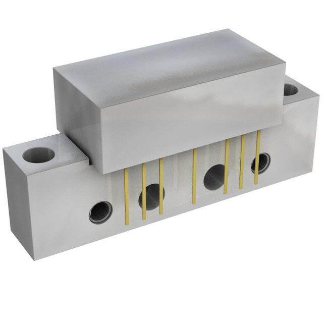
| 产品图片 |
|
| rohs | 符合RoHS无铅 / 符合限制有害物质指令(RoHS)规范要求 |
| 产品系列 | 放大器 IC,视频放大器,Texas Instruments UA733CD- |
| 数据手册 | |
| 产品型号 | UA733CD |
| 产品目录页面 | |
| 产品种类 | 视频放大器 |
| 供应商器件封装 | 14-SOIC |
| 其它名称 | 296-11825-5 |
| 包装 | 管件 |
| 单位重量 | 129.400 mg |
| 压摆率 | - |
| 可用增益调整 | 10 V/V, 100 V/V, 400 V/V |
| 商标 | Texas Instruments |
| 安装类型 | 表面贴装 |
| 安装风格 | SMD/SMT |
| 封装 | Tube |
| 封装/外壳 | 14-SOIC(0.154",3.90mm 宽) |
| 封装/箱体 | SOIC-14 |
| 工作温度范围 | 0 C to + 70 C |
| 工作电源电压 | 16 V |
| 工厂包装数量 | 50 |
| 应用 | 差分 |
| 最大双重电源电压 | +/- 8 V |
| 最大工作温度 | + 70 C |
| 最小工作温度 | 0 C |
| 标准包装 | 50 |
| 电压-电源,单/双 (±) | - |
| 电流-电源 | 16mA |
| 电流-输出/通道 | 3.6mA |
| 电源电流 | 16 mA |
| 电源类型 | Dual |
| 电路数 | 1 |
| 系列 | UA733 |
| 输出类型 | 差分 |
| 通道数量 | 1 Channel |


- 商务部:美国ITC正式对集成电路等产品启动337调查
- 曝三星4nm工艺存在良率问题 高通将骁龙8 Gen1或转产台积电
- 太阳诱电将投资9.5亿元在常州建新厂生产MLCC 预计2023年完工
- 英特尔发布欧洲新工厂建设计划 深化IDM 2.0 战略
- 台积电先进制程称霸业界 有大客户加持明年业绩稳了
- 达到5530亿美元!SIA预计今年全球半导体销售额将创下新高
- 英特尔拟将自动驾驶子公司Mobileye上市 估值或超500亿美元
- 三星加码芯片和SET,合并消费电子和移动部门,撤换高东真等 CEO
- 三星电子宣布重大人事变动 还合并消费电子和移动部门
- 海关总署:前11个月进口集成电路产品价值2.52万亿元 增长14.8%


PDF Datasheet 数据手册内容提取
(cid:1)(cid:1)(cid:2)(cid:3)(cid:3)(cid:4)(cid:5) (cid:1)(cid:1)(cid:2)(cid:3)(cid:3)(cid:6) (cid:7)(cid:8)(cid:9)(cid:9)(cid:10)(cid:11)(cid:10)(cid:12)(cid:13)(cid:8)(cid:1)(cid:14) (cid:15)(cid:8)(cid:7)(cid:10)(cid:16) (cid:1)(cid:6)(cid:17)(cid:14)(cid:8)(cid:9)(cid:8)(cid:10)(cid:11)(cid:18) The (cid:1)A733M is obsolete and no longer supplied. SLFS027B − NOVEMBER 1970 − REVISED MAY 2004 (cid:1) (cid:1) 200-MHz Bandwidth Selectable Nominal Amplification of 10, (cid:1) 250-kΩ Input Resistance 100, or 400 (cid:1) No Frequency Compensation Required (cid:1)A733C...D, N, OR NS PACKAGE (cid:1)A733M...U PACKAGE (cid:1)A733M...J PACKAGE (TOP VIEW) (TOP VIEW) IN+ 1 10 IN− IN+ 1 14 IN− GAIN ADJ 2A 2 9 GAIN ADJ 2B NC 2 13 NC GAIN ADJ 1A 3 8 GAIN ADJ 1B GAIN ADJ 2A 3 12 GAIN ADJ 2B GAIN ADJ 1A 4 11 GAIN ADJ 1B VCC− 4 7 VCC+ OUT+ 5 6 OUT− VCC− 5 10 VCC+ NC 6 9 NC OUT+ 7 8 OUT− NC No internal connection description/ordering information The µA733 is a monolithic two-stage video amplifier with differential inputs and differential outputs. Internal series-shunt feedback provides wide bandwidth, low phase distortion, and excellent gain stability. Emitter-follower outputs enable the device to drive capacitive loads, and all stages are current-source biased to obtain high common-mode and supply-voltage rejection ratios. Fixed differential amplification of 10 V/V, 100 V/V, or 400 V/V may be selected without external components, or amplification may be adjusted from 10 V/V to 400 V/V by the use of a single external resistor connected between 1A and 1B. No external frequency-compensating components are required for any gain option. The device is particularly useful in magnetic-tape or disc-file systems using phase or NRZ encoding and in high-speed thin-film or plated-wire memories. Other applications include general-purpose video and pulse amplifiers where wide bandwidth, low phase shift, and excellent gain stability are required. The µA733C is characterized for operation from 0°C to 70°C; the µA733M is characterized for operation over the full military temperature range of −55°C to 125°C. ORDERING INFORMATION ORDERABLE TOP-SIDE TA PACKAGE† PART NUMBER MARKING P-DIP (N) Tube of 25 UA733CN UA733CN Tube of 50 UA733CD 00°°CC ttoo 7700°°CC SSOOIICC ((DD)) UUAA773333CC Reel of 2500 UA733CDR SOP (NS) Reel of 2000 UA733CNSR UA733 †Package drawings, standard packing quantities, thermal data, symbolization, and PCB design guidelines are available at www.ti.com/sc/package. Please be aware that an important notice concerning availability, standard warranty, and use in critical applications of TexasInstruments semiconductor products and disclaimers thereto appears at the end of this data sheet. (cid:17)(cid:11)(cid:16)(cid:7)(cid:19)(cid:4)(cid:13)(cid:8)(cid:16)(cid:12) (cid:7)(cid:1)(cid:13)(cid:1) (cid:20)(cid:21)(cid:22)(cid:23)(cid:24)(cid:25)(cid:26)(cid:27)(cid:20)(cid:23)(cid:21) (cid:20)(cid:28) (cid:29)(cid:30)(cid:24)(cid:24)(cid:31)(cid:21)(cid:27) (cid:26)(cid:28) (cid:23)(cid:22) !(cid:30)"#(cid:20)(cid:29)(cid:26)(cid:27)(cid:20)(cid:23)(cid:21) $(cid:26)(cid:27)(cid:31)% Copyright 2004, Texas Instruments Incorporated (cid:17)(cid:24)(cid:23)$(cid:30)(cid:29)(cid:27)(cid:28) (cid:29)(cid:23)(cid:21)(cid:22)(cid:23)(cid:24)(cid:25) (cid:27)(cid:23) (cid:28)!(cid:31)(cid:29)(cid:20)(cid:22)(cid:20)(cid:29)(cid:26)(cid:27)(cid:20)(cid:23)(cid:21)(cid:28) !(cid:31)(cid:24) (cid:27)&(cid:31) (cid:27)(cid:31)(cid:24)(cid:25)(cid:28) (cid:23)(cid:22) (cid:13)(cid:31)’(cid:26)(cid:28) (cid:8)(cid:21)(cid:28)(cid:27)(cid:24)(cid:30)(cid:25)(cid:31)(cid:21)(cid:27)(cid:28) (cid:28)(cid:27)(cid:26)(cid:21)$(cid:26)(cid:24)$ ((cid:26)(cid:24)(cid:24)(cid:26)(cid:21)(cid:27))% (cid:17)(cid:24)(cid:23)$(cid:30)(cid:29)(cid:27)(cid:20)(cid:23)(cid:21) !(cid:24)(cid:23)(cid:29)(cid:31)(cid:28)(cid:28)(cid:20)(cid:21)* $(cid:23)(cid:31)(cid:28) (cid:21)(cid:23)(cid:27) (cid:21)(cid:31)(cid:29)(cid:31)(cid:28)(cid:28)(cid:26)(cid:24)(cid:20)#) (cid:20)(cid:21)(cid:29)#(cid:30)$(cid:31) (cid:27)(cid:31)(cid:28)(cid:27)(cid:20)(cid:21)* (cid:23)(cid:22) (cid:26)## !(cid:26)(cid:24)(cid:26)(cid:25)(cid:31)(cid:27)(cid:31)(cid:24)(cid:28)% POST OFFICE BOX 655303 • DALLAS, TEXAS 75265 1
(cid:1)(cid:1)(cid:2)(cid:3)(cid:3)(cid:4)(cid:5) (cid:1)(cid:1)(cid:2)(cid:3)(cid:3)(cid:6) (cid:7)(cid:8)(cid:9)(cid:9)(cid:10)(cid:11)(cid:10)(cid:12)(cid:13)(cid:8)(cid:1)(cid:14) (cid:15)(cid:8)(cid:7)(cid:10)(cid:16) (cid:1)(cid:6)(cid:17)(cid:14)(cid:8)(cid:9)(cid:8)(cid:10)(cid:11)(cid:18) The (cid:1)A733M is obsolete and no longer supplied. SLFS027B − NOVEMBER 1970 − REVISED MAY 2004 symbol GAIN ADJ 1A GAIN ADJ 2A IN+ + OUT+ _ IN− OUT− GAIN ADJ 1B GAIN ADJ 2B schematic VCC+ 2.4 kΩ 2.4 kΩ 10 kΩ 1.1 kΩ 1.1 kΩ OUT+ IN+ IN− 7 kΩ 1A 1B 7 kΩ GAIN 50 Ω GAIN OUT− ADJ 50 Ω ADJ 2A 2B 590 Ω 590 Ω 300 Ω 1.4 kΩ 300 Ω 400 Ω 400 Ω VCC− Component values shown are nominal. 2 POST OFFICE BOX 655303 • DALLAS, TEXAS 75265
(cid:1)(cid:1)(cid:2)(cid:3)(cid:3)(cid:4)(cid:5) (cid:1)(cid:1)(cid:2)(cid:3)(cid:3)(cid:6) (cid:7)(cid:8)(cid:9)(cid:9)(cid:10)(cid:11)(cid:10)(cid:12)(cid:13)(cid:8)(cid:1)(cid:14) (cid:15)(cid:8)(cid:7)(cid:10)(cid:16) (cid:1)(cid:6)(cid:17)(cid:14)(cid:8)(cid:9)(cid:8)(cid:10)(cid:11)(cid:18) The (cid:1)A733M is obsolete and no longer supplied. SLFS027B − NOVEMBER 1970 − REVISED MAY 2004 absolute maximum ratings over operating free-air temperature range (unless otherwise noted)† (cid:1)A733C (cid:1)A733M UNIT Supply voltage VCC+ (see Note 1) 8 8 V Supply voltage VCC− (see Note 1) − 8 − 8 V Differential input voltage ± 5 ± 5 V Common-mode input voltage ± 6 ± 6 V Output current 10 10 mA Continuous total power dissipation See Dissipation Rating Table D package 86 PPaacckkaaggee tthheerrmmaall iimmppeeddaannccee,, (cid:1)(cid:1)JJAA ((sseeee NNootteess 22 aanndd 33)) N package 80 °CC//WW NS package 76 Maximum junction temperature, TJ 150 °C Lead temperature 1,6 mm (1/16 inch) from case for 60 seconds J or U package 300 °C Storage temperature range, Tstg − 65 to 150 − 65 to 150 °C †Stresses beyond those listed under absolute maximum ratings may cause permanent damage to the device. This is a stress rating only, and functional operation of the device at these or any other conditions beyond those indicated in the recommended operating conditions section of this specification is not implied. Exposure to absolute-maximum-rated conditions for extended periods may affect device reliability. NOTES: 1. All voltage values, except differential input voltages, are with respect to the midpoint between VCC+ and VCC–. 2. Maximum power dissipation is a function of TJ(max), (cid:1)JA, and TA. The maximum allowable power dissipation at any allowable ambient temperature is PD = (TJ(max) – TA)/(cid:1)JA. Operating at the absolute maximum TJ of 150°C can affect reliability. 3. The package thermal impedance is calculated in accordance with JESD 51-7. DISSIPATION RATING TABLE TA ≤ 25°C DERATING DERATE TA = 70°C TA = 125°C PACKAGE POWER RATING FACTOR ABOVE TA POWER RATING POWER RATING J (µA733M) 500 mW 11.0 mW/°C 104°C 500 mW 269 mW POST OFFICE BOX 655303 • DALLAS, TEXAS 75265 3
(cid:1)(cid:1)(cid:2)(cid:3)(cid:3)(cid:4)(cid:5) (cid:1)(cid:1)(cid:2)(cid:3)(cid:3)(cid:6) (cid:7)(cid:8)(cid:9)(cid:9)(cid:10)(cid:11)(cid:10)(cid:12)(cid:13)(cid:8)(cid:1)(cid:14) (cid:15)(cid:8)(cid:7)(cid:10)(cid:16) (cid:1)(cid:6)(cid:17)(cid:14)(cid:8)(cid:9)(cid:8)(cid:10)(cid:11)(cid:18) The (cid:1)A733M is obsolete and no longer supplied. SLFS027B − NOVEMBER 1970 − REVISED MAY 2004 electrical characteristics, VCC± = ±6 V, TA = 25°C GGAAIINN (cid:1)A733C (cid:1)A733M PPAARRAAMMEETTEERR FFIIGGUURREE TTEESSTT CCOONNDDIITTIIOONNSS OPTION†† MIN TYP MAX MIN TYP MAX UUNNIITT LLaarrggee--ssiiggnnaall 1 250 400 600 300 400 500 ddiiffffeerreennttiiaall AAVVDD 11 VVOODD == 11 VV 2 80 100 120 90 100 110 VV//VV vvoollttaaggee amplification 3 8 10 12 9 10 11 1 50 50 BBWW BBaannddwwiiddtthh 22 RRSS == 5500 ΩΩ 2 90 90 MMHHzz 3 200 200 Input offset IIO current Any 0.4 5 0.4 3 µA IIB Input bias current Any 9 30 9 20 µA Common-mode VICR input voltage 1 Any ±1 ±1 V range Common-mode VOC output voltage 1 Any 2.4 2.9 3.4 2.4 2.9 3.4 V OOuuttppuutt ooffffsseett 1 0.6 1.5 0.6 1.5 VVOOOO voltage 11 2 & 3 0.35 1.5 0.35 1 VV Maximum peak- VOPP to-peak output 1 Any 3 4.7 3 4.7 V voltage swing 1 4 4 rrii IInnppuutt rreessiissttaannccee 33 VVOODD ≤≤ 11 VV 2 10 24 20 24 kkΩΩ 3 250 250 ro Output resistance 20 20 Ω Ci Input capacitance 3 VOD ≤ 1 V 2 2 2 pF VIC = ±1 V, 2 60 86 60 86 CCoommmmoonn--mmooddee f ≤ 100 kHz CCMMRRRR 44 ddBB rejection ration VIC = ±1 V, 2 70 70 f = 5 MHz Supply voltage kSVR rejection ratio 1 ∆VCC± = ±0.5 V 2 50 70 50 70 dB (∆VCC/(∆VIO) Broadband Vn equivalent input 5 BW = 1 kHz to 10 MHz Any 12 12 µV noise voltage PPrrooppaaggaattiioonn RRSS == 5500 ΩΩ,, 1 7.5 7.5 ttppdd ddeellaayy ttiimmee 22 OOuuttppuutt vvoollttaaggee 2 6.0 10 6.0 10 nnss sstteepp == 11 VV 3 3.6 3.6 RRSS == 5500 ΩΩ,, 1 10.5 10.5 ttrr RRiissee ttiimmee 22 OOuuttppuutt vvoollttaaggee 2 4.5 12 4.5 10 nnss sstteepp == 11 VV 3 2.5 2.5 Maximum output Isink(max) sink current Any 2.5 3.6 2.5 3.6 mA No load, ICC Supply current No signal Any 16 24 16 24 mA †The gain option is selected as follows: Gain Option 1: Gain-adjust pin 1A is connected to pin 1B, and pins 2A and 2B are open. Gain Option 2: Gain-adjust pin 1A and pin 1B are open, pin 2A is connected to pin 2B. Gain Option 3: All four gain-adjust pins are open. 4 POST OFFICE BOX 655303 • DALLAS, TEXAS 75265
(cid:1)(cid:1)(cid:2)(cid:3)(cid:3)(cid:4)(cid:5) (cid:1)(cid:1)(cid:2)(cid:3)(cid:3)(cid:6) (cid:7)(cid:8)(cid:9)(cid:9)(cid:10)(cid:11)(cid:10)(cid:12)(cid:13)(cid:8)(cid:1)(cid:14) (cid:15)(cid:8)(cid:7)(cid:10)(cid:16) (cid:1)(cid:6)(cid:17)(cid:14)(cid:8)(cid:9)(cid:8)(cid:10)(cid:11)(cid:18) The (cid:1)A733M is obsolete and no longer supplied. SLFS027B − NOVEMBER 1970 − REVISED MAY 2004 electrical characteristics, VCC± = ±6 V, TA = 0°C to 70°C for (cid:1)A733C, −55°C to 125°C for (cid:1)A733M GGAAIINN (cid:1)A733C (cid:1)A733M PPAARRAAMMEETTEERR FFIIGGUURREE TTEESSTT CCOONNDDIITTIIOONNSS OPTION†† MIN MAX MIN MAX UUNNIITT 1 250 600 200 600 LLaarrggee--ssiiggnnaall ddiiffffeerreennttiiaall AAVVDD vvoollttaaggee aammpplliiffiiccaattiioonn 11 VVOODD == 11 VV 2 80 120 80 120 VV//VV 3 8 12 8 12 IIO Input offset current Any 6 5 µA IIB Input bias current Any 40 40 µA Common-mode input VICR voltage range 1 Any ±1 ±1 V 1 1.5 1.5 VVOOOO OOuuttppuutt ooffffsseett vvoollttaaggee 11 VV 2 & 3 1.5 1.2 Maximum peak-to-peak VOPP output voltage swing 1 Any 2.8 2.5 V ri Input resistance 3 VOD ≤ 1 V 2 8 8 kΩ Common-mode rejection VIC = +1 V, CMRR 4 2 50 50 dB ratio f ≤ 100 kHz Supply voltage rejection kSVR ratio (∆VCC/(∆VIO) 1 ∆VCC± = ±0.5 V 2 50 50 dB Maximum output sink Isink(max) current Any 2.5 2.2 mA No load, ICC Supply current No signal Any 27 27 mA †The gain option is selected as follows: Gain Option 1: Gain-adjust pin 1A is connected to pin 1B, and pins 2A and 2B are open. Gain Option 2: Gain-adjust pin 1A and pin 1B are open, pin 2A is connected to pin 2B. Gain Option 3: All four gain-adjust pins are open. POST OFFICE BOX 655303 • DALLAS, TEXAS 75265 5
(cid:1)(cid:1)(cid:2)(cid:3)(cid:3)(cid:4)(cid:5) (cid:1)(cid:1)(cid:2)(cid:3)(cid:3)(cid:6) (cid:7)(cid:8)(cid:9)(cid:9)(cid:10)(cid:11)(cid:10)(cid:12)(cid:13)(cid:8)(cid:1)(cid:14) (cid:15)(cid:8)(cid:7)(cid:10)(cid:16) (cid:1)(cid:6)(cid:17)(cid:14)(cid:8)(cid:9)(cid:8)(cid:10)(cid:11)(cid:18) The (cid:1)A733M is obsolete and no longer supplied. SLFS027B − NOVEMBER 1970 − REVISED MAY 2004 PARAMETER MEASUREMENT INFORMATION test circuits 0.2 µF + + VID VOD 2 kΩ VID 0.2 µF − − 50 Ω 50 Ω 50 Ω 50 Ω 1 kΩ 1 kΩ Figure 1 Figure 2 0.2 µF 50 Ω + + VOD 2 kΩ 50 Ω 0.2 µF − − VIC 1 kΩ 1 kΩ Figure 3 Figure 4 2B 1B 0.2 µF + 0.2 µF + − VOD 2 kΩ − 50 Ω 50 Ω 1 kΩ 1 kΩ Radj 2A 1A VOLTAGE AMPLIFICATION ADJUSTMENT Figure 5 Figure 6 6 POST OFFICE BOX 655303 • DALLAS, TEXAS 75265
(cid:1)(cid:1)(cid:2)(cid:3)(cid:3)(cid:4)(cid:5) (cid:1)(cid:1)(cid:2)(cid:3)(cid:3)(cid:6) (cid:7)(cid:8)(cid:9)(cid:9)(cid:10)(cid:11)(cid:10)(cid:12)(cid:13)(cid:8)(cid:1)(cid:14) (cid:15)(cid:8)(cid:7)(cid:10)(cid:16) (cid:1)(cid:6)(cid:17)(cid:14)(cid:8)(cid:9)(cid:8)(cid:10)(cid:11)(cid:18) The (cid:1)A733M is obsolete and no longer supplied. SLFS027B − NOVEMBER 1970 − REVISED MAY 2004 TYPICAL CHARACTERISTICS PHASE SHIFT PHASE SHIFT vs vs FREQUENCY FREQUENCY 5 50 TVAC C= ±2 5 =°C ±6 V 0 TVAC C= ±2 5 =°C ±6 V 0 −50 GAIN 2 s e s −100 e e Degr −5 egre −150 Shift − GAIN 2 hift − D −200 se −10 e S −250 a s h a P Ph −300 −15 −350 −400 −20 −450 0 1 2 3 4 5 6 7 8 9 10 1 4 10 40 100 400 f − Frequency − MHz f − Frequency − MHz Figure 7 Figure 8 VOLTAGE AMPLIFICATION VOLTAGE AMPLIFICATION (SINGLE-ENDED OR DIFFERENTIAL) (SINGLE-ENDED OR DIFFERENTIAL) vs vs TEMPERATURE SUPPLY VOLTAGE o= 25 C 1.2 VCC± = ±6 V +_= 6 V+_ 1.4 TA = 25°C T A GAIN 1 CC e at 1.1 at V 1.2 u e Val (cid:1)A733C alu o V elative t 1.0 GAIN 2 GAIN 3 ative to 1.0 GAIN 3 R el n R catio GAIN 3 GAIN 2 ation 0.8 GAIN 2 mplifi 0.9 plific A m 0.6 ge e A GAIN 1 a GAIN 1 g Volt 0.8 olta V 0.4 −75 −50 −25 0 25 50 75 100 125 3 4 5 6 7 8 TA − Free-Air Temperature − °C |VCC±| − Supply Voltage − V Figure 9 Figure 10 POST OFFICE BOX 655303 • DALLAS, TEXAS 75265 7
(cid:1)(cid:1)(cid:2)(cid:3)(cid:3)(cid:4)(cid:5) (cid:1)(cid:1)(cid:2)(cid:3)(cid:3)(cid:6) (cid:7)(cid:8)(cid:9)(cid:9)(cid:10)(cid:11)(cid:10)(cid:12)(cid:13)(cid:8)(cid:1)(cid:14) (cid:15)(cid:8)(cid:7)(cid:10)(cid:16) (cid:1)(cid:6)(cid:17)(cid:14)(cid:8)(cid:9)(cid:8)(cid:10)(cid:11)(cid:18) The (cid:1)A733M is obsolete and no longer supplied. SLFS027B − NOVEMBER 1970 − REVISED MAY 2004 TYPICAL CHARACTERISTICS DIFFERENTIAL VOLTAGE AMPLIFICATION SINGLE-ENDED VOLTAGE AMPLIFICATION vs vs RESISTANCE BETWEEN G1A AND G1B FREQUENCY 1000 B 50 d n 700 VVOCCD ±= 1= V±6 V on − GAIN 1 plificatio 400 TSAee = F 2ig5°uCre 6 mplificati 40 GAIN 2 m 200 A e A ge 30 g a olta 100 Volt al V 70 ed nti nd 20 e e GAIN 3 er 40 e- Diff ngl − VD 20 − SiS 10 VCC± = ±6 V A AV TA = 25°C 0 10 10 40 100 400 1 k 4 k 10 k 1 4 10 40 100 400 Radj − Resistance Between G1A and G1B − Ω f − Frequency − MHz Figure 11 Figure 12 SUPPLY CURRENT SUPPLY CURRENT vs vs FREE-AIR TEMPERATURE SUPPLY VOLTAGE 20 24 No Load 18 No Signal 16 20 TA = 25°C A m A ent − 1142 (cid:1)A733C nt − m 16 urr rre C u pply 10 ply C 12 u 8 p S u I − CC 64 VCC± = ±6 V I − SCC 8 No Load 4 2 No Signal 0 0 −75 −50 −25 0 25 50 75 100 125 3 4 5 6 7 8 TA − Free-Air Temperature − °C |VCC±| − Supply Voltage − V Figure 13 Figure 14 8 POST OFFICE BOX 655303 • DALLAS, TEXAS 75265
(cid:1)(cid:1)(cid:2)(cid:3)(cid:3)(cid:4)(cid:5) (cid:1)(cid:1)(cid:2)(cid:3)(cid:3)(cid:6) (cid:7)(cid:8)(cid:9)(cid:9)(cid:10)(cid:11)(cid:10)(cid:12)(cid:13)(cid:8)(cid:1)(cid:14) (cid:15)(cid:8)(cid:7)(cid:10)(cid:16) (cid:1)(cid:6)(cid:17)(cid:14)(cid:8)(cid:9)(cid:8)(cid:10)(cid:11)(cid:18) The (cid:1)A733M is obsolete and no longer supplied. SLFS027B − NOVEMBER 1970 − REVISED MAY 2004 TYPICAL CHARACTERISTICS MAXIMUM PEAK-TO-PEAK OUTPUT VOLTAGE MAXIMUM PEAK-TO-PEAK OUTPUT VOLTAGE vs vs LOAD RESISTANCE SUPPLY VOLTAGE V 5 V 8 e − VCC± = ±6 V e − TA = 25°C ag TA = 25°C ag 7 olt olt V 4 V ut ut 6 p p ut ut O O k k 5 a 3 a e e P P o- o- 4 k-t k-t a a e 2 e P P 3 m m u u m m xi xi 2 Ma 1 Ma − − V OPP V OPP 1 0 0 10 40 100 400 1 k 4 k 10 k 3 4 5 6 7 8 RL − Load Resistance − Ω |VCC±| − Supply Voltage − V Figure 15 Figure 16 MAXIMUM PEAK-TO-PEAK OUTPUT VOLTAGE INPUT RESISTANCE vs vs FREQUENCY FREE-AIR TEMPERATURE V 6 40 oltage − 5 TVAC C= ±2 5 =°C ±6 V 35 VCC± = ±6 V V put Ω 30 Out 4 − k Peak-to-Peak 3 ut Resistance 2250 GAIN 2 (cid:1)A733C m 2 np 15 mu − I xi r i10 a M 1 − V OPP 0 5 1 2 4 7 10 20 40 70 100 200 400 0 −60 −40 −20 0 20 40 60 80 100 120 140 f − Frequency − MHz TA − Free-Air Temperature − °C Figure 17 Figure 18 POST OFFICE BOX 655303 • DALLAS, TEXAS 75265 9
PACKAGE OPTION ADDENDUM www.ti.com 6-Feb-2020 PACKAGING INFORMATION Orderable Device Status Package Type Package Pins Package Eco Plan Lead/Ball Finish MSL Peak Temp Op Temp (°C) Device Marking Samples (1) Drawing Qty (2) (6) (3) (4/5) UA733CD ACTIVE SOIC D 14 50 Green (RoHS NIPDAU Level-1-260C-UNLIM 0 to 70 UA733C & no Sb/Br) UA733CDR ACTIVE SOIC D 14 2500 Green (RoHS NIPDAU Level-1-260C-UNLIM 0 to 70 UA733C & no Sb/Br) UA733CN ACTIVE PDIP N 14 25 Green (RoHS NIPDAU N / A for Pkg Type 0 to 70 UA733CN & no Sb/Br) UA733CNSR ACTIVE SO NS 14 2000 Green (RoHS NIPDAU Level-1-260C-UNLIM 0 to 70 UA733 & no Sb/Br) (1) The marketing status values are defined as follows: ACTIVE: Product device recommended for new designs. LIFEBUY: TI has announced that the device will be discontinued, and a lifetime-buy period is in effect. NRND: Not recommended for new designs. Device is in production to support existing customers, but TI does not recommend using this part in a new design. PREVIEW: Device has been announced but is not in production. Samples may or may not be available. OBSOLETE: TI has discontinued the production of the device. (2) RoHS: TI defines "RoHS" to mean semiconductor products that are compliant with the current EU RoHS requirements for all 10 RoHS substances, including the requirement that RoHS substance do not exceed 0.1% by weight in homogeneous materials. Where designed to be soldered at high temperatures, "RoHS" products are suitable for use in specified lead-free processes. TI may reference these types of products as "Pb-Free". RoHS Exempt: TI defines "RoHS Exempt" to mean products that contain lead but are compliant with EU RoHS pursuant to a specific EU RoHS exemption. Green: TI defines "Green" to mean the content of Chlorine (Cl) and Bromine (Br) based flame retardants meet JS709B low halogen requirements of <=1000ppm threshold. Antimony trioxide based flame retardants must also meet the <=1000ppm threshold requirement. (3) MSL, Peak Temp. - The Moisture Sensitivity Level rating according to the JEDEC industry standard classifications, and peak solder temperature. (4) There may be additional marking, which relates to the logo, the lot trace code information, or the environmental category on the device. (5) Multiple Device Markings will be inside parentheses. Only one Device Marking contained in parentheses and separated by a "~" will appear on a device. If a line is indented then it is a continuation of the previous line and the two combined represent the entire Device Marking for that device. (6) Lead/Ball Finish - Orderable Devices may have multiple material finish options. Finish options are separated by a vertical ruled line. Lead/Ball Finish values may wrap to two lines if the finish value exceeds the maximum column width. Important Information and Disclaimer:The information provided on this page represents TI's knowledge and belief as of the date that it is provided. TI bases its knowledge and belief on information provided by third parties, and makes no representation or warranty as to the accuracy of such information. Efforts are underway to better integrate information from third parties. TI has taken and Addendum-Page 1
PACKAGE OPTION ADDENDUM www.ti.com 6-Feb-2020 continues to take reasonable steps to provide representative and accurate information but may not have conducted destructive testing or chemical analysis on incoming materials and chemicals. TI and TI suppliers consider certain information to be proprietary, and thus CAS numbers and other limited information may not be available for release. In no event shall TI's liability arising out of such information exceed the total purchase price of the TI part(s) at issue in this document sold by TI to Customer on an annual basis. Addendum-Page 2
PACKAGE MATERIALS INFORMATION www.ti.com 14-Jul-2012 TAPE AND REEL INFORMATION *Alldimensionsarenominal Device Package Package Pins SPQ Reel Reel A0 B0 K0 P1 W Pin1 Type Drawing Diameter Width (mm) (mm) (mm) (mm) (mm) Quadrant (mm) W1(mm) UA733CDR SOIC D 14 2500 330.0 16.4 6.5 9.0 2.1 8.0 16.0 Q1 UA733CNSR SO NS 14 2000 330.0 16.4 8.2 10.5 2.5 12.0 16.0 Q1 PackMaterials-Page1
PACKAGE MATERIALS INFORMATION www.ti.com 14-Jul-2012 *Alldimensionsarenominal Device PackageType PackageDrawing Pins SPQ Length(mm) Width(mm) Height(mm) UA733CDR SOIC D 14 2500 367.0 367.0 38.0 UA733CNSR SO NS 14 2000 367.0 367.0 38.0 PackMaterials-Page2
None
None
None
None
IMPORTANTNOTICEANDDISCLAIMER TI PROVIDES TECHNICAL AND RELIABILITY DATA (INCLUDING DATASHEETS), DESIGN RESOURCES (INCLUDING REFERENCE DESIGNS), APPLICATION OR OTHER DESIGN ADVICE, WEB TOOLS, SAFETY INFORMATION, AND OTHER RESOURCES “AS IS” AND WITH ALL FAULTS, AND DISCLAIMS ALL WARRANTIES, EXPRESS AND IMPLIED, INCLUDING WITHOUT LIMITATION ANY IMPLIED WARRANTIES OF MERCHANTABILITY, FITNESS FOR A PARTICULAR PURPOSE OR NON-INFRINGEMENT OF THIRD PARTY INTELLECTUAL PROPERTY RIGHTS. These resources are intended for skilled developers designing with TI products. You are solely responsible for (1) selecting the appropriate TI products for your application, (2) designing, validating and testing your application, and (3) ensuring your application meets applicable standards, and any other safety, security, or other requirements. These resources are subject to change without notice. TI grants you permission to use these resources only for development of an application that uses the TI products described in the resource. Other reproduction and display of these resources is prohibited. No license is granted to any other TI intellectual property right or to any third party intellectual property right. TI disclaims responsibility for, and you will fully indemnify TI and its representatives against, any claims, damages, costs, losses, and liabilities arising out of your use of these resources. TI’s products are provided subject to TI’s Terms of Sale (www.ti.com/legal/termsofsale.html) or other applicable terms available either on ti.com or provided in conjunction with such TI products. TI’s provision of these resources does not expand or otherwise alter TI’s applicable warranties or warranty disclaimers for TI products. Mailing Address: Texas Instruments, Post Office Box 655303, Dallas, Texas 75265 Copyright © 2020, Texas Instruments Incorporated