ICGOO在线商城 > BTS443P
 Datasheet下载
- 型号: BTS443P
- 制造商: Infineon
- 库位|库存: xxxx|xxxx
- 要求:
| 数量阶梯 | 香港交货 | 国内含税 |
| +xxxx | $xxxx | ¥xxxx |
查看当月历史价格
查看今年历史价格
BTS443P产品简介:
ICGOO电子元器件商城为您提供BTS443P由Infineon设计生产,在icgoo商城现货销售,并且可以通过原厂、代理商等渠道进行代购。 提供BTS443P价格参考以及InfineonBTS443P封装/规格参数等产品信息。 你可以下载BTS443P参考资料、Datasheet数据手册功能说明书, 资料中有BTS443P详细功能的应用电路图电压和使用方法及教程。
| 参数 | 数值 |
| 产品目录 | 集成电路 (IC)半导体 |
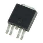
| 描述 | SWITCH HIGH SIDE POWER TO252-5电源开关 IC - 配电 Smart High Side 1 Ch 36V 42W |
| 产品分类 | PMIC - MOSFET,电桥驱动器 - 内部开关集成电路 - IC |
| 品牌 | Infineon Technologies |
| 产品手册 | |
| 产品图片 |
|
| rohs | 符合RoHS无铅 / 符合限制有害物质指令(RoHS)规范要求 |
| 产品系列 | 开关 IC,电源开关 IC - 配电,Infineon Technologies BTS443PPROFET® |
| mouser_ship_limit | 该产品可能需要其他文件才能进口到中国。 |
| 数据手册 | http://www.infineon.com/dgdl/BTS443P_DS_v10.pdf?folderId=db3a304314dca389011537739e37155f&fileId=db3a3043183a9555011860442f5b3616 |
| 产品型号 | BTS443P |
| 产品目录页面 | |
| 产品种类 | 电源开关 IC - 配电 |
| 供应商器件封装 | PG-TO252-5 |
| 其它名称 | BTS443PAUMA1 |
| 包装 | 带卷 (TR) |
| 商标 | Infineon Technologies |
| 安装类型 | 表面贴装 |
| 安装风格 | SMD/SMT |
| 导通电阻 | 13 毫欧 |
| 导通电阻—最大值 | 16 mOhms |
| 封装 | Reel |
| 封装/外壳 | TO-252-5,DPak(4 引线 + 接片),TO-252AD |
| 封装/箱体 | TO-252-5 |
| 工作温度 | -40°C ~ 150°C |
| 工作电源电压 | 5 V to 36 V |
| 工厂包装数量 | 2500 |
| 最大功率耗散 | 42 W |
| 最大工作温度 | + 150 C |
| 最小工作温度 | - 40 C |
| 标准包装 | 2,500 |
| 电压-电源 | 5 V ~ 36 V |
| 电流-峰值输出 | 65A |
| 电流-输出/通道 | 25A |
| 电流限制 | 65 A |
| 电源电流—最大值 | 5 uA |
| 空闲时间—最大值 | 410 us |
| 类型 | 高端 |
| 系列 | BTS443 |
| 输入类型 | 非反相 |
| 输出数 | 1 |
| 输出电流 | 25 A |
| 输出端数量 | 1 Output |
| 运行时间—最大值 | 410 us |
| 零件号别名 | BTS443PAUMA1 SP000264198 |

.jpg)


- 商务部:美国ITC正式对集成电路等产品启动337调查
- 曝三星4nm工艺存在良率问题 高通将骁龙8 Gen1或转产台积电
- 太阳诱电将投资9.5亿元在常州建新厂生产MLCC 预计2023年完工
- 英特尔发布欧洲新工厂建设计划 深化IDM 2.0 战略
- 台积电先进制程称霸业界 有大客户加持明年业绩稳了
- 达到5530亿美元!SIA预计今年全球半导体销售额将创下新高
- 英特尔拟将自动驾驶子公司Mobileye上市 估值或超500亿美元
- 三星加码芯片和SET,合并消费电子和移动部门,撤换高东真等 CEO
- 三星电子宣布重大人事变动 还合并消费电子和移动部门
- 海关总署:前11个月进口集成电路产品价值2.52万亿元 增长14.8%


PDF Datasheet 数据手册内容提取
PROFET® BTS 443 P Smart Highside Power Switch Reversave Product Summary • Reverse battery protection by self turn on of Operating voltage Vbb(on) 5.0 ... 36 V power MOSFET On-state resistance RON 16 mΩ Features • Short circuit protection Load current (ISO) IL(ISO) 25 A • Current limitation Current limitation IL(SCr) 65 A • Overload protection Package • Thermal shutdown • PG-TO252-5-11 Overvoltage protection (including load dump) • Loss of ground protection • Loss of Vbb protection (with external diode for charged inductive loads) • Very low standby current • Fast demagnetisation of inductive loads • Electrostatic discharge (ESD) protection • Optimized static electromagnetic compatibility (EMC) • Green product (RoHS compliant) • AEC qualified Diagnostic Function • Proportional load current sense (with defined fault signal during thermal shutdown) Application • Power switch with current sense diagnostic feedback for 12V and 24 V DC grounded loads • All types of resistive, capacitive and inductive loads (no PWM with inductive loads) • Replaces electromechanical relays, fuses and discrete circuits General Description N channel vertical power FET with charge pump, current controlled input and diagnostic feedback with load current sense, integrated in Smart SIPMOS chip on chip technology. Providing embedded protective functions. 3 & Tab + Vbb R bb Voltage Overvoltage Current Gate source protection limit protection 1, 5 OUT Limit for Voltage Charge pump unclamped I sensor ind. loads L Level shifter Current Rectifier Output Sense 2 Voltage Load IN ESD Logic detection I IN Temperature sensor I IS PROFET IS 4 Load GND V IN VIS RIS Logic GND Data Sheet Page 1 of 15 Rev. 1.0, 2007-02
PROFET® BTS 443 P Pin Symbol Function 1 OUT O Output to the load. The pin 1 and 5 must be shorted with each other especially in high current applications!*) 2 IN I Input, activates the power switch in case of short to ground Tab/(3) Vbb + Positive power supply voltage, the tab is shorted to this pin. 4 IS S Diagnostic feedback providing a sense current proportional to the load current; high current on failure (see Truth Table on page 6) 5 OUT O Output to the load. The pin 1 and 5 must be shorted with each other especially in high current applications!*) *) Not shorting all outputs will considerably increase the on-state resistance, reduce the peak current capability and decrease the current sense accuracy Maximum Ratings at T = 25 °C unless otherwise specified j Parameter Symbol Values Unit Supply voltage (overvoltage protection see page 4) V 36 V bb Supply voltage for full short circuit protection V 241) V bb (see also diagram on page 9) T=-40...150 °C: j Load dump protection VLoadDump = UA + Vs, UA = 13.5 V VLoad dump2) 60 V R= 2 Ω, R = 2.7 Ω, t = 200 ms, IN= low or high I L d Load current (Short-circuit current, see page 4) I self-limited A L Operating temperature range T -40 ...+150 °C j Storage temperature range T -55 ...+150 stg Power dissipation (DC) TC ≤ 25°C P 42 W tot Inductive load switch-off energy dissipation, single pulse U=12V, I=10A, L=3mH T=150 °C: E 0.15 J j AS Electrostatic discharge capability (ESD) V 4.0 kV ESD (Human Body Model) acc. ESD assn. std. S5.1-1993; R=1.5kΩ; C=100pF Current through input pin (DC) I +15, -100 mA IN Current through current sense pin (DC) I +15, -100 IS see internal circuit diagrams page 7 1 ) Short circuit is tested with 100mΩ and 20µH 2) V is set-up without the DUT connected to the generator per ISO 7637-1 and DIN 40839 Load dump Data Sheet Page 2 of 13 Rev. 1.0, 2007-02
PROFET® BTS 443 P Thermal Characteristics Parameter and Conditions Symbol Values Unit min typ max Thermal resistance chip - case: RthJC3) -- -- 1.5 K/W junction - ambient (free air): R -- 80 -- thJA SMD version, device on PCB4): -- 45 -- Electrical Characteristics Parameter and Conditions Symbol Values Unit at Tj= -40°C...150°C, Vbb = 12 V unless otherwise specified min typ max Load Switching Capabilities and Characteristics On-state resistance (pin 3 to pin 1,5) V = 0, I = 5 A T=25 °C: R -- 13 16 mΩ IN L j ON Tj=150 °C: 25 31 Output voltage drop limitation at small load V -- 50 -- mV ON(NL) currents (Tab to pin 1,5) Tj=-40...150 °C: Nominal load current (Tab to pin 1,5) A ISO Proposal: T =85°C, V ≤0.5V, T≤150°C I 21 25 -- C ON j L(ISO) SMD 4): T =85°C, V ≤0.5V, T≤150°C I 6.2 7.6 -- A ON j L(nom) Turn-on time IIN to 90% VOUT: ton 150 -- 410 µs Turn-off time IIN to 10% VOUT: toff 70 -- 410 RL = 2,5Ω, Tj=-40...150 °C Slew rate on dV /dt 0.1 -- 1 V/µs on 10 to 30% VOUT, RL = 2.5 Ω, Tj=-40...150 °C Slew rate off -dV/dt 0.1 -- 1 V/µs off 70 to 40% V , R = 2.5 Ω, T=-40...150 °C OUT L j 3) Thermal resistance R case to heatsink (about 0.5 ... 0.9 K/W with silicone paste) not included! thCH 4) Device on 50mm*50mm*1.5mm epoxy PCB FR4 with 6cm2 (one layer, 70µm thick) copper area for Vbb connection. PCB is vertical without blown air. Data Sheet Page 3 of 13 Rev. 1.0, 2007-02
PROFET® BTS 443 P Parameter and Conditions Symbol Values Unit at Tj= -40°C...150°C, Vbb = 12 V unless otherwise specified min typ max Operating Parameters Operating voltage (VIN=0V) Vbb(on) 5.0 -- 36 V Undervoltage shutdown 5) V 1.5 3.0 4.5 V bIN(u) Undervoltage restart of charge pump (V =0V) V 3.0 4.5 6.0 V IN bb(ucp) Overvoltage protection 6) V 61 68 -- V Z,IN I =15 mA bb Standby current Tj=-40...+25°C: Ibb(off) -- 2 5 µA I =0 T=150°C: -- 4 8 IN j Protection Functions 7) Short circuit current limit (Tab to pin 1,5) V =8V, time until limitation max. 300µs ON Tj =-40°C: IL(SC) 35 75 110 A Tj =25°C: 35 65 110 Tj =+150°C: 35 65 125 Repetitive short circuit current limit, Tj = Tjt IL(SCr) -- 65 -- A Output clamp (inductive load switch off) at V = V - V (e.g. overvoltage) V 38 42 48 V OUT bb ON(CL) ON(CL) IL= 40 mA 8) Thermal overload trip temperature T 150 -- -- °C jt Thermal hysteresis ∆T -- 10 -- K jt Reverse Battery Reverse battery voltage -V -- -- 20 V bb On-state resistance (pin 1,5 to pin 3) V = - 8V, V = 0, I = -5 A, R = 1 kΩ, T=25 °C: R -- -- 22 mΩ bb IN L IS j ON(rev) V = -12V, V = 0, I = -5 A, R = 1 kΩ, T=25 °C: -- 16 19 bb IN L IS j Tj=150 °C: 25 32 Integrated resistor in V line R -- 200 -- Ω bb bb 5) VbIN=Vbb-VIN see diagram on page 11. 6) see also VON(CL) in circuit diagram on page 7. 7) Integrated protection functions are designed to prevent IC destruction under fault condition described in the data sheet. Fault conditions are considered as “outside” normal operating range. Protection functions are not for continuous repetitive operation. 8) see also page 12. Data Sheet Page 4 of 15 Rev. 1.0, 2007-02
PROFET® BTS 443 P Diagnostic Characteristics Current sense ratio, static on-condition k -- 8200 -- ILIS k =I :I ILIS L IS V <1.5V, V <V -5V, V >4.5V 9) ON IS OUT bIN IL = 20A, Tj = -40°C: 7400 8300 9100 Tj = +25°C: 7500 8300 9100 Tj = +150°C: 7500 8200 8800 IL = 5A, Tj = -40°C: 6800 8300 9700 Tj = +25°C: 7200 8300 9300 Tj = +150°C: 7200 8200 9000 IL = 2.5A, Tj = -40°C: 6800 8500 10000 Tj = +25°C: 6800 8500 9800 Tj = +150°C: 6800 8100 9200 IL = 1A, Tj = -40°C: 6800 8600 10500 Tj = +25°C: 6800 8600 10500 Tj = +150°C: 6800 8600 10500 IIN = 0 (e.g. during de-energising of inductive loads): -- n.a. -- Sense current under fault conditions; VDS>1.5V, typ. Tj= -40...+150°C: IIS,fault 2.5 4 -- mA Fault-Sense signal delay after negative input slope t 0.8 ms delay(fault) Current sense leakage current -- -- 0.5 µA IIN = 0: IIS(LL) V =0, I =0: I -- 4 12 IN L IS(LH) Current sense settling time to I ±10% after IS static positive input slope, IL = 0 20 A 10) tson(IS) -- -- 400 µs Tj= -40...+150°C: Overvoltage protection I =15mA T =-40...+150°C: V 61 68 -- V bb j bIS(Z) Input Required current capability of input switch I -- 0.7 1.2 mA IN(on) T =-40..+150°C: j Maximum input current for turn-offT =-40..+150°C: I -- -- 50 µA j IN(off) 9) If V is higher, the sense current is no longer proportional to the load current due to sense current ON saturation. 10) Not subject to production test, specified by design. Data Sheet Page 5 of 15 Rev. 1.0, 2007-02
PROFET® BTS 443 P Truth Table Input Output Current Current Sense level level IIS Normal L L 0 operation H H nominal Overload L L 0 H H I ISfault Short circuit to GND L L 0 H L I ISfault Overtemperature L L 0 H L I ISfault Short circuit to Vbb L H 0 H H <nominal11 Open load L Z 0 H H 0 L = "Low" Level Z = high impedance, potential depends on external circuit H = "High" Level Terms Ibb 3 V bIN V V ON bb I L V IN OUT bb 2 1,5 PROFET R IN IS VIN VbIS 4 IIS IIN DS VOUT V R IS IS Two or more devices can easily be connected in parallel to increase load current capability. 11) Low ohmic short to V may reduce the output current I and therefore also the sense current I . bb L IS Data Sheet Page 6 of 15 Rev. 1.0, 2007-02
PROFET® BTS 443 P Input circuit (ESD protection) Inductive and overvoltage output clamp + V bb Vbb V Z1 V V ZD Rbb ON Z,IN VbIN IN OUT PROFET I IN VON is clamped to VON(Cl) = 42 V typ. VIN ESD-Zener diode: 68 V typ., max 15 mA; Current sense output Overvoltage protection of logic part Normal operation + V Vbb Rbb ZD bb IIS,fault VZ,IS VZ,IN VZ,IS Rbb R IN IS IN Logic IIS V OUT V IS R IS PROFET IS VZ,IS = 68 V (typ.), RIS = 1 kΩ nominal (or 1 kΩ /n, if n R IS R V V Z,VIS devices are connected in parallel). IS = IL/kilis can be Signal GND only driven by the internal circuit as long as Rbb = 200 Ω typ., VZ,IN = VZ,IS = 68 V typ., RIS = 1 kΩ Vout - VIS > 5V. If you want to measure load currents nominal. Note that when overvoltage exceeds 73 V typ. V −5V a voltage above 5V can occur between IS and GND, if up to IL(M), RIS should be less than I bb /K . RV, VZ,VIS are not used. L(M) ilis Note: For large values of RIS the voltage VIS can reach almost Vbb. See also overvoltage protection. If you don't use the current sense output in your application, you can leave it open. Data Sheet Page 7 of 15 Rev. 1.0, 2007-02
PROFET® BTS 443 P Reversave (Reverse battery protection) Version b: -Vbb V R V bb bb bb IN PROFET OUT IN OUT IS RIN Logic PTroawnesristor V Zb IS R L Note that there is no reverse battery protection when D RIS RV using a diode without additional Z-diode V , V . ZL Zb Signal Power RV≥1kΩ, R IS = 1 kΩ nominal. Add RIN for reverse Version c: battery protection in applications with Vbb above 16V; Sometimes a necessary voltage clamp is given by non 1 1 1 0.05A, inductive loads R connected to the same switch and recommended value: + + = L RIN RIS RV |V |−12V eliminates the need of clamping circuit: bb To minimise power dissipation at reverse battery operation, the summarised current into the IN and IS pin should be about 50mA. The current can be V V provided by using a small signal diode D in parallel to bb bb RL the input switch, by using a MOSFET input switch or by IN PROFET OUT proper adjusting the current through R and R IS V. Since the current through R generates additional bb heat in the device, this has to be taken into account in IS the overall thermal considerations. Vbb disconnect with energised inductive load Provide a current path with load current capability by using a diode, a Z-diode, or a varistor. (V <73 V or ZL V <30 V if R =0). For higher clamp voltages Zb IN currents at IN and IS have to be limited to 250 mA. Version a: Vbb V bb IN PROFET OUT IS V ZL Data Sheet Page 8 of 15 Rev. 1.0, 2007-02
PROFET® BTS 443 P Maximum allowable load inductance for Inductive load switch-off energy dissipation a single switch off Ebb L = f (IL ); Tj,start = 150°C, Vbb = 12 V, RL = 0 Ω EAS L[mH] 100 E Load V bb i L (t) Vbb IN PROFET OUT EL 10 IS L { Z IIN RIS L RL ER 1 Energy stored in load inductance: EL = 1/2·L·I2 L While demagnetising load inductance, the energy dissipated in PROFET is 0.1 EAS= Ebb + EL - ER= ∫ VON(CL)·iL(t) dt, with an approximate solution for RL > 0 Ω: EAS= 2IL·R· LL(Vbb + |VOUT(CL)|) ln (1+ |VOILU·TR(CLL)| ) 0.01 0 25 50 75 100 The device is not suitable for permanent PWM with IL [A] inductive loads if active clamping occurs every cycle. Data Sheet Page 9 of 15 Rev. 1.0, 2007-02
PROFET® BTS 443 P Timing diagrams Figure 1a: Switching a resistive load, Figure 2a: Switching motors and lamps: change of load current in on-condition: I I IN IN V OUT dV/dtoff 90% ton V OUT dV/dton t off 10% I tslc(IS) tslc(IS) I L IL Load 1 Load 2 I I IS IS t son(IS) t t t soff(IS) The sense signal is not valid during a settling time Sense current above IIS,fault can occur at very high inrush currents. after turn-on/off and after change of load current. Figure 1b: typical behaviour of sense output: Figure 2b: Switching an inductive load: I IN IS IIS,fault >= 2.5mA V OUT IL(lim) = 20A IL I L I IS t Data Sheet Page 10 of 15 Rev. 1.0, 2007-02
PROFET® BTS 443 P Figure 3a: Short circuit: Figure 5a: Undervoltage restart of charge pump, overvoltage clamp IN V 12 OUT 10 V = 0 IN I L 8 I V L(SCp) ON(CL) dynamic, short I 6 L(SCr) Undervoltage not below VbIN(u) 4 IIS I 2 IIN= 0 ISfault V ON(CL) t 0 V 0 Vb2IN(u) 4 V6bIN(ucp8) 10 1b2b Figure 4a: Overtemperature Reset if T<T j jt I IN I IIS,fault IS V Auto Restart OUT T j t Data Sheet Page 11 of 15 Rev. 1.0, 2007-02
PROFET® BTS 443 P Figure 6a: Current sense versus load current: Figure 7a: Output voltage drop versus load current: [mA] IIS [V] VON 0.1 R ON 2.0 V ON(NL) 0.05 1.0 I L I L 0 0.0 0 5 10 15 20 [A] [A] 0 1 2 3 4 5 6 7 8 Figure 6b: Current sense ratio12): k ILIS 8200 [A] IL 0 0 2.5 5 10 20 12 ) This range for the current sense ratio refers to all devices. The accuracy of the k can be raised by ILIS means of calibration the value of k for every ILIS single device. Data Sheet Page 12 of 15 Rev. 1.0, 2007-02
PROFET® BTS 443 P Package Outlines All dimensions in mm D-Pak-5 Pin: PG-TO252-5-11 Sales Code BTS 443P Green Product To meet the world-wide customer requirements for environmentally friendly products and to be compliant with government regulations the device is available as a green product. Green products are RoHS-Compliant (i.e Pb- free finish on leads and suitable for Pb-free soldering according to IPC/JEDEC J-STD-020). Data Sheet Page 13 of 15 Rev. 1.0, 2007-02
PROFET® BTS 443 P Revision History Version Date Changes Rev. 1.0 2007-02-21 RoHS-compliant version of BTS443P Page 1, page 13: RoHS compliance statement and Green product feature added Page 1, page 13: Change to RoHS compliant package PG-TO252-5-11 Legal disclaimer updated Data Sheet Page 14 of 15 Rev. 1.0, 2007-02
Edition 2007-02 Published by Infineon Technologies AG 81726 Munich, Germany © Infineon Technologies AG 2007. All Rights Reserved. Legal Disclaimer The information given in this document shall in no event be regarded as a guarantee of conditions or characteristics (“Beschaffenheitsgarantie”). With respect to any examples or hints given herein, any typical values stated herein and/or any information regarding the application of the device, Infineon Technologies hereby disclaims any and all warranties and liabilities of any kind, including without limitation warranties of non- infringement of intellectual property rights of any third party. Information For further information on technology, delivery terms and conditions and prices please contact your nearest Infineon Technologies Office (www.infineon.com). Warnings Due to technical requirements components may contain dangerous substances. For information on the types in question please contact your nearest Infineon Technologies Office. Infineon Technologies Components may only be used in life-support devices or systems with the express written approval of Infineon Technologies, if a failure of such components can reasonably be expected to cause the failure of that life-support device or system, or to affect the safety or effectiveness of that device or system. Life support devices or systems are intended to be implanted in the human body, or to support and/or maintain and sustain and/or protect human life. If they fail, it is reasonable to assume that the health of the user or other persons may be endangered.
Mouser Electronics Authorized Distributor Click to View Pricing, Inventory, Delivery & Lifecycle Information: I nfineon: BTS443P BTS443PAUMA1