ICGOO在线商城 > 集成电路(IC) > PMIC - 配电开关,负载驱动器 > BTS409L1 E3062A
 Datasheet下载
- 型号: BTS409L1 E3062A
- 制造商: Infineon
- 库位|库存: xxxx|xxxx
- 要求:
| 数量阶梯 | 香港交货 | 国内含税 |
| +xxxx | $xxxx | ¥xxxx |
查看当月历史价格
查看今年历史价格
BTS409L1 E3062A产品简介:
ICGOO电子元器件商城为您提供BTS409L1 E3062A由Infineon设计生产,在icgoo商城现货销售,并且可以通过原厂、代理商等渠道进行代购。 BTS409L1 E3062A价格参考。InfineonBTS409L1 E3062A封装/规格:PMIC - 配电开关,负载驱动器, 。您可以下载BTS409L1 E3062A参考资料、Datasheet数据手册功能说明书,资料中有BTS409L1 E3062A 详细功能的应用电路图电压和使用方法及教程。
Infineon Technologies的BTS409L1 E3062A是一款PMIC(电源管理集成电路),主要用于配电开关和负载驱动器应用。该器件具有高效、紧凑和可靠的特性,适用于多种工业和消费类应用场景。

 应用场景

1. 汽车电子:
   - 车身控制模块 (BCM):用于控制车窗、门锁、座椅调节等。BTS409L1能够提供稳定的电流输出,并具备过流保护和短路保护功能,确保系统安全可靠。
   - 电动助力转向系统 (EPS):为电机驱动提供高效、稳定的电源管理,支持快速响应和精确控制。

2. 工业自动化:
   - 电机驱动与控制:在工厂自动化设备中,如传送带、机器人手臂等,BTS409L1可以作为驱动电路的一部分,确保电机运行稳定且高效。
   - 智能传感器:为各种传感器提供稳定的电源供应,确保数据采集的准确性和稳定性。

3. 消费电子产品:
   - 智能家居设备:如智能灯泡、智能插座等,BTS409L1可以实现对负载的有效控制,同时提供过热、过流保护,提升产品的安全性和使用寿命。
   - 便携式设备:如电动工具、手持吸尘器等,该器件能够在高功率需求下保持高效工作,延长电池续航时间。

4. 医疗设备:
   - 便携式医疗仪器:如血糖仪、血压计等,BTS409L1可以确保设备在不同负载条件下稳定工作,提供精确的测量结果。
   - 可穿戴健康监测设备:如智能手环、智能手表等,该器件能够有效管理电源,确保设备长时间稳定运行。

 特点与优势
- 高效能:低导通电阻(RDS(on))使得功耗更低,效率更高。
- 集成保护功能:内置过流、过温、短路保护,提高系统可靠性。
- 小封装:节省空间,适合紧凑设计。
- 易于使用:简单易用的接口设计,便于快速集成到现有系统中。

综上所述,BTS409L1 E3062A凭借其高效、可靠和多功能的特点,广泛应用于汽车、工业、消费电子和医疗等领域,满足各种复杂的应用需求。
| 参数 | 数值 |
| 产品目录 | 集成电路 (IC)半导体 |
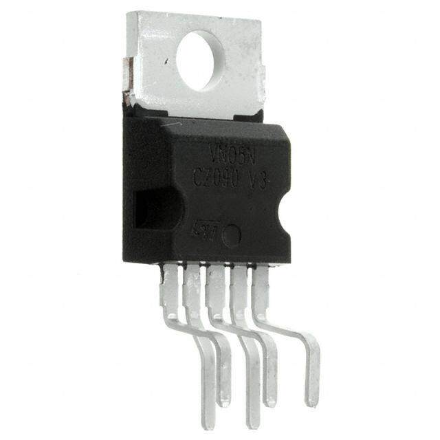
| 描述 | IC SWITCH SMART HISIDE TO220AB-5电源开关 IC - 配电 PROFET SMART HI SIDE PWR SW |
| 产品分类 | PMIC - MOSFET,电桥驱动器 - 内部开关集成电路 - IC |
| 品牌 | Infineon Technologies |
| 产品手册 | |
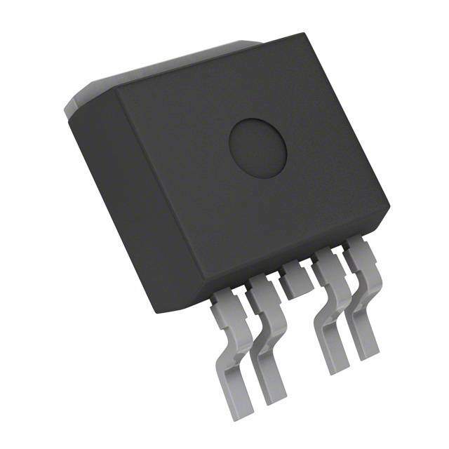
| 产品图片 |
|
| rohs | 否含铅 / 不符合限制有害物质指令(RoHS)规范要求 |
| 产品系列 | 开关 IC,电源开关 IC - 配电,Infineon Technologies BTS409L1 E3062APROFET® |
| mouser_ship_limit | 该产品可能需要其他文件才能进口到中国。 |
| 数据手册 | http://www.infineon.com/dgdl/BTS409L1_20030925.pdf?folderId=db3a30431ddc9372011e26863f92474e&fileId=db3a304331c8f8560131dcc7f54e0e1c&ack=t |
| 产品型号 | BTS409L1 E3062A |
| PCN设计/规格 | |
| PCN过时产品 | |
| 产品目录页面 | |
| 产品种类 | 电源开关 IC - 配电 |
| 供应商器件封装 | SMD TO-220AB/5 |
| 其它名称 | BTS409L1 E3062A-ND |
| 包装 | 带卷 (TR) |
| 商标 | Infineon Technologies |
| 安装类型 | 表面贴装 |
| 安装风格 | SMD/SMT |
| 导通电阻 | 160 毫欧 |
| 导通电阻—最大值 | 200 mOhms |
| 封装 | Reel |
| 封装/外壳 | TO-263-5,D²Pak(4 引线+接片),TO-263BB |
| 封装/箱体 | TO-220-5 |
| 工作温度 | -40°C ~ 150°C |
| 工作电源电压 | 5 V to 34 V |
| 工厂包装数量 | 1000 |
| 最大功率耗散 | 18 W |
| 最大工作温度 | + 150 C |
| 最小工作温度 | - 40 C |
| 标准包装 | 1,000 |
| 电压-电源 | 5 V ~ 34 V |
| 电流-峰值输出 | 7.5A |
| 电流-输出/通道 | 2.3A |
| 电流限制 | 4 A |
| 电源电流—最大值 | 3.5 mA |
| 空闲时间—最大值 | 400 us |
| 类型 | 高端 |
| 系列 | BTS409L1 |
| 输入类型 | 非反相 |
| 输出数 | 1 |
| 输出电流 | 1.8 A |
| 输出端数量 | 1 Output |
| 运行时间—最大值 | 400 us |
| 零件号别名 | BTS409L1E3062ANTMA1 SP000011232 |


.jpg)


- 商务部:美国ITC正式对集成电路等产品启动337调查
- 曝三星4nm工艺存在良率问题 高通将骁龙8 Gen1或转产台积电
- 太阳诱电将投资9.5亿元在常州建新厂生产MLCC 预计2023年完工
- 英特尔发布欧洲新工厂建设计划 深化IDM 2.0 战略
- 台积电先进制程称霸业界 有大客户加持明年业绩稳了
- 达到5530亿美元!SIA预计今年全球半导体销售额将创下新高
- 英特尔拟将自动驾驶子公司Mobileye上市 估值或超500亿美元
- 三星加码芯片和SET,合并消费电子和移动部门,撤换高东真等 CEO
- 三星电子宣布重大人事变动 还合并消费电子和移动部门
- 海关总署:前11个月进口集成电路产品价值2.52万亿元 增长14.8%


PDF Datasheet 数据手册内容提取
PROFET® BTS409L1 Smart High-Side Power Switch Product Summary Overvoltage protection V 43 V bb(AZ) Operating voltage Vbb(on) 5.0 ... 34 V On-state resistance RON 200 m Features Overload protection Load current (ISO) IL(ISO) 2.3 A Current limitation Current limitation IL(SCr) 4 A Short circuit protection Thermal shutdown Overvoltage protection (including load dump) PG-TO263-5-2 Fast demagnetization of inductive loads Reverse battery protection1) Undervoltage and overvoltage shutdown with auto-restart and hysteresis Open drain diagnostic output Open load detection in ON-state CMOS compatible input Loss of ground and loss of Vbb protection Electrostatic discharge (ESD) protection Green Product (RoHS compliant) AEC Qualified Application C compatible power switch with diagnostic feedback for 12 V and 24 V DC grounded loads All types of resistive, inductive and capacitve loads Replaces electromechanical relays, fuses and discrete circuits General Description N channel vertical power FET with charge pump, ground referenced CMOS compatible input and diagnostic feedback, monolithically integrated in Smart SIPMOS technology. Fully protected by embedded protection functions. + V bb 3 Voltage Overvoltage Current Gate source protection limit protection V Logic Voltage Charge Limit for OUT unclampe 5 sensor puLmevpe l idn d. loads Temperature shifter sensor 2 IN Rectifier Open load Short to Vbb Load ESD Logic detection 4 ST R O GND PROFET GND 1 Signal GND Load GND 1) With external current limit (e.g. resistor R =150 ) in GND connection, resistor in series with ST GND connection, reverse load current limited by connected load. Data Sheet 1 2013-10-10
BTS409L1 Pin Symbol Function 1 GND - Logic ground 2 IN I Input, activates the power switch in case of logical high signal 3 Vbb + Positive power supply voltage, the tab is shorted to this pin 4 ST S Diagnostic feedback, low on failure 5 OUT O Output to the load (Load, L) Data Sheet 2 2013-10-10
BTS409L1 Maximum Ratings at T = 25 °C unless otherwise specified j Parameter Symbol Values Unit Supply voltage (overvoltage protection see page 4) V 43 V bb Supply voltage for short circuit protection V 34 V bb T =-40 ...+150°C j Start Load dump protection2) VLoadDump = UA + Vs, UA = 13.5 V VLoad dump4) 60 V RI3)= 2 , RL= 5.3 , td= 200 ms, IN= low or high Load current (Short circuit current, see page 5) I self-limited A L Operating temperature range T -40 ...+150 °C j Storage temperature range T -55 ...+150 stg Power dissipation (DC), T 25 °C P 18 W C tot Inductive load switch-off energy dissipation, single pulse V =12V, T =150°C, T =150°C const. bb j,start C IL = 2.3 A, ZL = 98 mH, 0 : EAS 335 mJ Electrostatic discharge capability (ESD) IN: V 1.0 kV ESD (Human Body Model) all other pins: 2.0 acc. MIL-STD883D, method 3015.7 and ESD assn. std. S5.1-1993 Input voltage (DC) V -10 ... +16 V IN Current through input pin (DC) I 2.0 mA IN Current through status pin (DC) I 5.0 ST see internal circuit diagrams page 7 Thermal Characteristics Parameter and Conditions Symbol Values Unit min typ max Thermal resistance chip - case: R -- -- 7 K/W thJC junction - ambient (free air): RthJA -- -- 75 SMD version, device on PCB5): 39 2) Supply voltages higher than V require an external current limit for the GND and status pins, e.g. with a bb(AZ) 150 resistor in the GND connection and a 15 k resistor in series with the status pin. A resistor for the protection of the input is integrated. 3) R = internal resistance of the load dump test pulse generator I 4) V is setup without the DUT connected to the generator per ISO 7637-1 and DIN 40839 Load dump 5) Device on 50mm*50mm*1.5mm epoxy PCB FR4 with 6cm2 (one layer, 70m thick) copper area for Vbb connection. PCB is vertical without blown air. Data Sheet 3 2013-10-10
BTS409L1 Electrical Characteristics Parameter and Conditions Symbol Values Unit at Tj = 25 °C, Vbb = 12 V unless otherwise specified min typ max Load Switching Capabilities and Characteristics On-state resistance (pin 3 to 5) IL = 1.8 A Tj=25 °C: RON -- 160 200 m Tj=150 °C: 320 400 Nominal load current, ISO Norm (pin 3 to 5) 1.8 2.3 V = 0.5 V, T = 85 °C I -- A ON C L(ISO) Output current (pin 5) while GND disconnected or I -- -- 10 mA L(GNDhigh) GND pulled up, Vbb=30 V, VIN= 0, see diagram page 8 Turn-on time IN to 90% V : t 80 200 400 s OUT on Turn-off time IN to 10% V : t 80 200 400 OUT off RL = 12 , Tj =-40...+150°C Slew rate on dV /dt 0.1 -- 1 V/s on 10 to 30% VOUT, RL = 12 , Tj =-40...+150°C Slew rate off -dV/dt 0.1 -- 1 V/s off 70 to 40% VOUT, RL = 12 , Tj =-40...+150°C Operating Parameters Operating voltage6) Tj =-40...+150°C: Vbb(on) 5.0 -- 34 V Undervoltage shutdown Tj =-40...+150°C: Vbb(under) 3.5 -- 5.0 V Undervoltage restart Tj =-40...+25°C: Vbb(u rst) -- -- 5.0 V Tj =+150°C: 7.0 Undervoltage restart of charge pump V -- 5.6 7.0 V bb(ucp) see diagram page 12 Tj =-40...+150°C: Undervoltage hysteresis V -- 0.2 -- V bb(under) V = V - V bb(under) bb(u rst) bb(under) Overvoltage shutdown Tj =-40...+150°C: Vbb(over) 34 -- 43 V Overvoltage restart Tj =-40...+150°C: Vbb(o rst) 33 -- -- V Overvoltage hysteresis Tj =-40...+150°C: Vbb(over) -- 0.5 -- V Overvoltage protection7) Tj =-40...+150°C: Vbb(AZ) 42 47 -- V I =40 mA bb Standby current (pin 3) VIN=0 Tj=-40...+25°C: Ibb(off) -- 10 23 A T= 150°C: -- 12 28 j 6) At supply voltage increase up to V = 5.6 V typ without charge pump, V V - 2 V bb OUT bb 7) See also VON(CL) in table of protection functions and circuit diagram page 8. Data Sheet 4 2013-10-10
BTS409L1 Parameter and Conditions Symbol Values Unit at Tj = 25 °C, Vbb = 12 V unless otherwise specified min typ max Leakage output current (included in Ibb(off)) IL(off) -- -- 12 A VIN=0 Operating current (Pin 1)8), V =5 V, I -- 1.8 3.5 mA IN GND Tj =-40...+150°C Protection Functions9) Initial peak short circuit current limit (pin 3 to 5) I L(SCp) Tj =-40°C: 5.5 9.5 13 A T =25°C: 4.5 7.5 11 j T =+150°C: 3 5 7 j Repetitive short circuit shutdown current limit I L(SCr) T = T (see timing diagrams, page 10) -- 4 -- A j jt Output clamp (inductive load switch off) at VOUT = Vbb - VON(CL) IL= 40 mA: VON(CL) 41 47 53 V Thermal overload trip temperature T 150 -- -- °C jt Thermal hysteresis T -- 10 -- K jt Reverse battery (pin 3 to 1) 10) -V -- -- 32 V bb Diagnostic Characteristics Open load detection current Tj=-40 °C: IL (OL) 10 -- 200 mA (on-condition) Tj=25 ..150°C: 10 -- 150 Open load detection voltage11) (off-condition) V 2 3 4 V OUT(OL) T=-40..150°C: j Internal output pull down (pin 5 to 1), V =5 V, T=-40..150°C R 4 10 30 k OUT j O 8) Add I , if I > 0, add I , if V >5.5 V ST ST IN IN 9) Integrated protection functions are designed to prevent IC destruction under fault conditions described in the data sheet. Fault conditions are considered as "outside" normal operating range. Protection functions are not designed for continuous repetitive operation. 10) Requires 150 resistor in GND connection. The reverse load current through the intrinsic drain-source diode has to be limited by the connected load. Note that the power dissipation is higher compared to normal operating conditions due to the voltage drop across the intrinsic drain-source diode. The temperature protection is not active during reverse current operation! Input and Status currents have to be limited (see max. ratings page 2 and circuit page 8). 11) External pull up resistor required for open load detection in off state. Data Sheet 5 2013-10-10
BTS409L1 Parameter and Conditions Symbol Values Unit at Tj = 25 °C, Vbb = 12 V unless otherwise specified min typ max Input and Status Feedback12) Input resistance R 2.5 3.5 6 k I see circuit page 7 Input turn-on threshold voltage T =-40..+150°C: V 1.7 -- 3.5 V j IN(T+) Input turn-off threshold voltage T =-40..+150°C: V 1.5 -- -- V j IN(T-) Input threshold hysteresis V -- 0.5 -- V IN(T) Off state input current (pin 2), V = 0.4 V, I 1 -- 50 A IN IN(off) T =-40..+150°C j On state input current (pin 2), V = 3.5 V, I 20 50 90 A IN IN(on) T =-40..+150°C j Delay time for status with open load after switch t 100 400 800 s d(ST OL4) off (see timing diagrams, page 11), Tj =-40..+150°C Status invalid after positive input slope t -- 250 600 s d(ST) (open load) Tj=-40 ... +150°C: Status output (open drain) Zener limit voltage Tj =-40...+150°C, IST = +1.6 mA: VST(high) 5.4 6.1 -- V ST low voltage Tj =-40...+25°C, IST = +1.6 mA: VST(low) -- -- 0.4 Tj = +150°C, IST = +1.6 mA: -- -- 0.6 12) If a ground resistor R is used, add the voltage drop across this resistor. GND Data Sheet 6 2013-10-10
BTS409L1 Truth Table Input- Output Status level level Normal L L H operation H H H Open load L 13) H (L14)) H H L Short circuit L H L15) to Vbb H H H (L16)) Overtem- L L H perature H L L Under- L L H voltage H L H Overvoltage L L H H L H L = "Low" Level X = don't care Z = high impedance, potential depends on external circuit H = "High" Level Status signal after the time delay shown in the diagrams (see fig 5. page 11...12) Terms Status output +5V Ibb 3 I IN IN Vbb RST(ON) ST 2 IL VON PROFET OUT IST 5 ESD- ST ZD 4 GND VIN VST GND Vbb 1 IGND VOUT ESD-Zener diode: 6.1 V typ., max 5 mA; RGND RST(ON) < 380 at 1.6 mA, ESD zener diodes are not to be used as voltage clamp at DC conditions. Operation in this mode may result in a drift of the zener voltage (increase of up to 1 V). Input circuit (ESD protection) Inductive and overvoltage output clamp R IN I + Vbb V Z ESD-ZD I I I V ON GND OUT ESD zener diodes are not to be used as voltage clamp PROFET GND at DC conditions. Operation in this mode may result in a drift of the zener voltage (increase of up to 1 V). VON clamped to 47 V typ. 13) Power Transistor off, high impedance 14) with external resistor between pin 3 and pin 5 15) An external short of output to V , in the off state, causes an internal current from output to ground. If R bb GND is used, an offset voltage at the GND and ST pins will occur and the V signal may be errorious. ST low 16) Low resistance to V may be detected in ON-state by the no-load-detection bb Data Sheet 7 2013-10-10
BTS409L1 GND disconnect Overvolt. and reverse batt. protection + Vbb 3 V bb IN V R R Z2 2 IN I IN PROFET OUT 5 Logic ST RST ST 4 GND VZ1 PROFET Vbb VIN VST 1 VGND GND R GND Any kind of load. In case of Input=high is VOUT VIN - VIN(T+) . Signal GND Due to VGND >0, no VST = low signal available. VZ1 = 6.2 V typ., VZ2 = 47 V typ., RGND = 150 , RST= 15 k, RI= 3.5 k typ. GND disconnect with GND pull up Open-load detection 3 ON-state diagnostic condition: V < R * I ; IN ON ON L(OL) V high IN bb 2 PROFET OUT + Vbb 5 ST 4 GND 1 V ON ON V V V IN ST V bb GND OUT Open load Any kind of load. If VGND > VIN - VIN(T+) device stays off Logic Due to VGND >0, no VST = low signal available. detection unit Vbb disconnect with energized inductive load OFF-state diagnostic condition: V > 3 V typ.; IN low 3 OUT high IN Vbb 2 PROFET OUT 5 R EXT ST 4 GND OFF 1 V OUT V bb Logic Open load R unit detection O Normal load current can be handled by the PROFET itself. Signal GND Data Sheet 8 2013-10-10
BTS409L1 Vbb disconnect with charged external Maximum allowable load inductance for inductive load a single switch off L = f (IL ); Tj,start = 150°C,TC = 150°C const., S 3 Vbb = 12 V, RL = 0 L [mH] high IN Vbb 10000 2 PROFET OUT 5 D ST 4 GND 1 1000 V bb If other external inductive loads L are connected to the PROFET, 100 additional elements like D are necessary. Inductive Load switch-off energy dissipation Ebb 10 EAS E Load V IN bb 1 PROFET OUT 1 2 3 4 5 = ST EL GND L IL [A] { Z L RL ER Transient thermal impedance chip case ZthJC = f(tp)ZthJC [K/W] 10 Energy stored in load inductance: EL = 1/2·L·I2L While demagnetizing load inductance, the energy dissipated in PROFET is 1 E = E + E - E = V ·i (t) dt, AS bb L R ON(CL) L with an approximate solution for R 0: L I ·L I ·R EAS= 2L·R L·(Vbb + |VOUT(CL)|)· ln (1+ |VOLUT(CLL)| ) D= 0.5 0.2 0.1 0.1 0.05 0.02 0.01 0 0.01 1E-5 1E-4 1E-3 1E-2 1E-1 1E0 1E1 1E2 tp [s] Data Sheet 9 2013-10-10
BTS409L1 Timing diagrams Figure 1a: Vbb turn on: Figure 2b: Switching an inductive load IN IN V bb t d(ST) ST *) V OUT V OUT ST open drain I L t IL(OL) t proper turn on under all conditions *) if the time constant of load is too large, open-load-status may Figure 2a: Switching a lamp, occur Figure 3a: Short circuit shut down by overtempertature, reset by cooling IN IN ST I L I L(SCp) V I OUT L(SCr) I L t ST t Heating up may require several milliseconds, depending on external conditions Data Sheet 10 2013-10-10
BTS409L1 Figure 4a: Overtemperature: Figure 5b: Open load: detection in ON-state, open Reset if Tj <Tjt load occurs in on-state IN IN t d(ST OL1) t d(ST OL2) ST ST V V OUT OUT T normal open normal I J L t t td(ST OL1) = 30 s typ., td(ST OL2) = 20 s typ Figure 5a: Open load: detection in ON-state, turn Figure 5c: Open load: detection in ON- and OFF-state on/off to open load (with REXT), turn on/off to open load IN IN t t d(ST) d(ST OL4) t ST ST d(ST) V V OUT OUT I I L L open open t t The status delay time td(ST OL4) allows to ditinguish between the failure modes "open load" and "overtemperature". Data Sheet 11 2013-10-10
BTS409L1 Figure 6a: Undervoltage: Figure 7a: Overvoltage: IN IN V V V V bb Vbb ON(CL) bb(over) bb(o rst) V Vbb(u cp) bb(under) V bb(u rst) V OUT V OUT ST ST open drain t t Figure 6b: Undervoltage restart of charge pump V VON(CL) on e e e at at at st st st off- on- V off- bb(over) V V bb(u rst) bb(o rst) V bb(u cp) V bb(under) V bb charge pump starts at Vbb(ucp) =5.6 V typ. Data Sheet 12 2013-10-10
BTS409L1 Published by Package and Ordering Code Infineon Technologies AG, Bereichs Kommunikation All dimensions in mm D-81726 München PG-TO263-5-2 Ordering code © Infineon Technologies AG 2013 BTS409L1 E3062A SP001104814 All Rights Reserved. Attention please! The information herein is given to describe certain components and shall not be considered as warranted characteristics. Terms of delivery and rights to technical change reserved. We hereby disclaim any and all warranties, including but not limited to warranties of non-infringement, regarding circuits, descriptions and charts stated herein. Infineon Technologies is an approved CECC manufacturer. Information For further information on technology, delivery terms and conditions and prices please contact your nearest Infineon Technologies Office in Germany or our Infineon Technologies Representatives worldwide (see address list). Warnings Due to technical requirements components may contain dangerous substances. For information on the types in question please contact your nearest Infineon Technologies Office. Infineon Technologies Components may only be used in life-support devices or systems with the express written approval of Infineon Technologies, if a failure of such components can reasonably be expected to cause the failure of that life-support device or system, or to affect the safety or effectiveness of that device or system. Life support devices or systems are intended to be implanted in the human body, or to support and/or maintain and sustain and/or protect human life. If they fail, it is reasonable to assume that the health of the user or other persons may be endangered. Data Sheet 13 2013-10-10