ICGOO在线商城 > BTM7751G
 Datasheet下载
- 型号: BTM7751G
- 制造商: Infineon
- 库位|库存: xxxx|xxxx
- 要求:
| 数量阶梯 | 香港交货 | 国内含税 |
| +xxxx | $xxxx | ¥xxxx |
查看当月历史价格
查看今年历史价格
BTM7751G产品简介:
ICGOO电子元器件商城为您提供BTM7751G由Infineon设计生产,在icgoo商城现货销售,并且可以通过原厂、代理商等渠道进行代购。 提供BTM7751G价格参考以及InfineonBTM7751G封装/规格参数等产品信息。 你可以下载BTM7751G参考资料、Datasheet数据手册功能说明书, 资料中有BTM7751G详细功能的应用电路图电压和使用方法及教程。
| 参数 | 数值 |
| 产品目录 | 集成电路 (IC) |
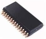
| 描述 | IC BRIDGE DRIVER PAR 28DSO |
| 产品分类 | PMIC - 电机, 电桥式驱动器 |
| 品牌 | Infineon Technologies |
| 数据手册 | http://www.infineon.com/dgdl/Infineon-BTM7751G-DS-v01_00-en.pdf?folderId=db3a3043156fd5730116144c5d101c30&fileId=db3a30431be39b97011bea19d1f07ff3&ack=t |
| 产品图片 |
|
| 产品型号 | BTM7751G |
| rohs | 无铅 / 符合限制有害物质指令(RoHS)规范要求 |
| 产品系列 | TrilithIC™ |
| 产品目录页面 | |
| 供应商器件封装 | PG-DSO-28 |
| 其它名称 | BTM7751GDKR |
| 功能 | 功率桥 - 逻辑驱动功率级 |
| 包装 | Digi-Reel® |
| 安装类型 | 表面贴装 |
| 封装/外壳 | 28-SOIC(0.295",7.50mm 宽) |
| 工作温度 | -40°C ~ 150°C |
| 应用 | 通用 |
| 接口 | 并联 |
| 标准包装 | 1 |
| 电压-电源 | 1.8 V ~ 42 V |
| 电压-负载 | 1.8 V ~ 42 V |
| 电机类型-AC,DC | 有刷直流 |
| 电机类型-步进 | - |
| 电流-输出 | 14A |
| 输出配置 | H 桥, 可配置 |


.jpg)


- 商务部:美国ITC正式对集成电路等产品启动337调查
- 曝三星4nm工艺存在良率问题 高通将骁龙8 Gen1或转产台积电
- 太阳诱电将投资9.5亿元在常州建新厂生产MLCC 预计2023年完工
- 英特尔发布欧洲新工厂建设计划 深化IDM 2.0 战略
- 台积电先进制程称霸业界 有大客户加持明年业绩稳了
- 达到5530亿美元!SIA预计今年全球半导体销售额将创下新高
- 英特尔拟将自动驾驶子公司Mobileye上市 估值或超500亿美元
- 三星加码芯片和SET,合并消费电子和移动部门,撤换高东真等 CEO
- 三星电子宣布重大人事变动 还合并消费电子和移动部门
- 海关总署:前11个月进口集成电路产品价值2.52万亿元 增长14.8%


PDF Datasheet 数据手册内容提取
Data Sheet, Rev. 1.0, June 2008 BTM7751G TrilithIC Automotive Power
BTM7751G Table of Contents TableofContents . . . . . . . . . . . . . . . . . . . . . . . . . . . . . . . . . . . . . . . . . . . . . . . . . . . . . . . . . . . . . . . . 2 1 Overview . . . . . . . . . . . . . . . . . . . . . . . . . . . . . . . . . . . . . . . . . . . . . . . . . . . . . . . . . . . . . . . . . . . . . . . 3 2 Pin Configuration . . . . . . . . . . . . . . . . . . . . . . . . . . . . . . . . . . . . . . . . . . . . . . . . . . . . . . . . . . . . . . . . 4 2.1 Pin Assignment . . . . . . . . . . . . . . . . . . . . . . . . . . . . . . . . . . . . . . . . . . . . . . . . . . . . . . . . . . . . . . . . . . . 4 2.2 Terms . . . . . . . . . . . . . . . . . . . . . . . . . . . . . . . . . . . . . . . . . . . . . . . . . . . . . . . . . . . . . . . . . . . . . . . . . . 6 3 Block Diagram . . . . . . . . . . . . . . . . . . . . . . . . . . . . . . . . . . . . . . . . . . . . . . . . . . . . . . . . . . . . . . . . . . . 7 4 Circuit Description . . . . . . . . . . . . . . . . . . . . . . . . . . . . . . . . . . . . . . . . . . . . . . . . . . . . . . . . . . . . . . . 8 4.1 Input Circuit . . . . . . . . . . . . . . . . . . . . . . . . . . . . . . . . . . . . . . . . . . . . . . . . . . . . . . . . . . . . . . . . . . . . . . 8 4.2 Output Stages . . . . . . . . . . . . . . . . . . . . . . . . . . . . . . . . . . . . . . . . . . . . . . . . . . . . . . . . . . . . . . . . . . . . 8 4.3 Short Circuit Protection . . . . . . . . . . . . . . . . . . . . . . . . . . . . . . . . . . . . . . . . . . . . . . . . . . . . . . . . . . . . . 8 4.4 Overtemperature Protection . . . . . . . . . . . . . . . . . . . . . . . . . . . . . . . . . . . . . . . . . . . . . . . . . . . . . . . . . 8 4.5 Undervoltage Lockout . . . . . . . . . . . . . . . . . . . . . . . . . . . . . . . . . . . . . . . . . . . . . . . . . . . . . . . . . . . . . . 8 4.6 Open Load Detection . . . . . . . . . . . . . . . . . . . . . . . . . . . . . . . . . . . . . . . . . . . . . . . . . . . . . . . . . . . . . . 8 4.7 Status Flag . . . . . . . . . . . . . . . . . . . . . . . . . . . . . . . . . . . . . . . . . . . . . . . . . . . . . . . . . . . . . . . . . . . . . . 9 5 Electrical Characteristics . . . . . . . . . . . . . . . . . . . . . . . . . . . . . . . . . . . . . . . . . . . . . . . . . . . . . . . . . 10 5.1 Absolute Maximum Ratings . . . . . . . . . . . . . . . . . . . . . . . . . . . . . . . . . . . . . . . . . . . . . . . . . . . . . . . . 10 5.2 Functional Range . . . . . . . . . . . . . . . . . . . . . . . . . . . . . . . . . . . . . . . . . . . . . . . . . . . . . . . . . . . . . . . . 11 5.3 Thermal Resistance . . . . . . . . . . . . . . . . . . . . . . . . . . . . . . . . . . . . . . . . . . . . . . . . . . . . . . . . . . . . . . 11 5.4 Electrical Characteristics . . . . . . . . . . . . . . . . . . . . . . . . . . . . . . . . . . . . . . . . . . . . . . . . . . . . . . . . . . 12 6 Application Information . . . . . . . . . . . . . . . . . . . . . . . . . . . . . . . . . . . . . . . . . . . . . . . . . . . . . . . . . . 15 7 Package Outlines . . . . . . . . . . . . . . . . . . . . . . . . . . . . . . . . . . . . . . . . . . . . . . . . . . . . . . . . . . . . . . . 16 8 Revision History . . . . . . . . . . . . . . . . . . . . . . . . . . . . . . . . . . . . . . . . . . . . . . . . . . . . . . . . . . . . . . . . 17 Data Sheet 2 Rev. 1.0, 2008-06-27
TrilithIC BTM7751G 1 Overview Features • Quad D-MOS switch driver • Free configurable as bridge or quad-switch • Optimized for DC motor management applications • Low R DSON High side: 70 mΩ typ. @25°C, 180 mΩ max. @150°C Low side: 45 mΩ typ. @25°C, 105 mΩ max. @150°C • Maximum peak current: typ. 14 A @ 25°C • Very low quiescent current: typ. 5 μA @ 25 °C PG-DSO-28-22 • Small outline, enhanced power PG-DSO-package • Operates up to 40 V • PWM frequencies up to 1 kHz • Status flag diagnosis • Short-circuit-protection • Overtemperature shut down with hysteresis • Internal clamp diodes • Open load detection in Off-mode • Under-voltage detection with hysteresis • Green Product (RoHS compliant) • AEC Qualified Description The BTM7751G is part of the TrilithIC family containing three dies in one package: One double high-side switch and two low-side switches. The drains of these three vertical DMOS chips are mounted on separated lead frames. The sources are connected to individual pins, so the BTM7751G can be used in H-bridge- as well as in any other configuration. Both the double high-side and the two low-side switches of the BTM7751G are manufactured in SMART SIPMOS® technology which combines low R vertical DMOS power stages with CMOS circuitry for DSON control, protection and diagnosis. Type Package Marking BTM7751G PG-DSO-28-22 BTM7751G Data Sheet 3 Rev. 1.0, 2008-06-27
BTM7751G 2 Pin Configuration 2.1 Pin Assignment DL1 1 28 DL1 IL1 2 27 SL1 DL1 3 26 SL1 LS-Leadframe N.C. 4 25 DL1 DHVS 5 24 DHVS GND 6 23 SH1 IH1 7 22 SH1 HS-Leadframe ST 8 21 SH2 IH2 9 20 SH2 DHVS 10 19 DHVS N.C. 11 18 DL2 LS-Leadframe DL2 12 17 SL2 IL2 13 16 SL2 DL2 14 15 DL2 Figure1 Pin Assignment BTM7751G (Top View) Data Sheet 4 Rev. 1.0, 2008-06-27
BTM7751G Table1 Pin Definitions and Functions Pin No. Symbol Function 1, 3, 25, 28 DL1 Drain of low-side switch1, lead frame 1 1) 2 IL1 Analog input of low-side switch1 4 N.C. not connected 5, 10, 19, 24 DHVS Drain of high-side switches and power supply voltage, lead frame 2 1) 6 GND Ground 7 IH1 Digital input of high-side switch1 8 ST Status of high-side switches; open Drain output 9 IH2 Digital input of high-side switch2 11 N.C. not connected 12, 14, 15, 18 DL2 Drain of low-side switch2, lead frame 3 1) 13 IL2 Analog input of low-side switch2 16,17 SL2 Source of low-side switch2 20,21 SH2 Source of high-side switch2 22,23 SH1 Source of high-side switch1 26,27 SL1 Source of low-side switch1 1) To reduce the thermal resistance these pins are direct connected via metal bridges to the lead frame. Pins written in bold type need power wiring. Data Sheet 5 Rev. 1.0, 2008-06-27
BTM7751G 2.2 Terms V=12V S I S C C S L 470nF 100µF I FH1,2 DHVS I 5,10,19,24 ST LK IST ST 8 VDSH2 VDSH1 -V -V FH2 FH1 Diagnosis Biasing and Protection V ST I IH1 IH1 7 Gate V STL Driver V STZ I RO1 RO2 20,21 SH2 ISH2 IH1 IH2 9 Gate VIH1 Driver 12,14,15,18 DL2 IDL2 V GND 6 IDL LK 2 VUVON IH2 IGND 22,23 SH1 ISH1 VUVOFF ILKCL Protection 1,3,25,28 DL1 IDL1 I DL LK 1 IIL1 IL1 2 Gate Driver Protection VIL1 IIL2 IL2 13 Gate Driver V IL th 1 V 26,27 16,17 V V IL2 DSL1 DSL2 V SL1 SL2 -V -V IL th 2 FL1 FL2 I I SCP L 1 SCP L 2 I I SL1 SL2 Figure2 Terms BTM7751G Table2 HS-Source-Current Named during Short Circuit Named during Leakage-Cond. I I I SH1,2 SCP H DL LK Data Sheet 6 Rev. 1.0, 2008-06-27
BTM7751G 3 Block Diagram DHVS 5,10,19,24 8 ST Diagnosis Biasing and Protection 7 Gate IH1 Driver R R O1 O2 20,21 9 Gate SH2 IH2 Driver 12,14,15,18 DL2 6 GND 22,23 SH1 1,3,25,28 Protection DL1 2 Gate IL1 Driver Protection 13 Gate IL2 Driver 26,27 16,17 SL1 SL2 Figure3 Block Diagram BTM7751G Data Sheet 7 Rev. 1.0, 2008-06-27
BTM7751G 4 Circuit Description 4.1 Input Circuit The control inputs IH1,2 consist of TTL/CMOS compatible Schmitt-Triggers with hysteresis. Buffer amplifiers are driven by these stages and convert the logic signal into the necessary form for driving the power output stages. The inputs are protected by ESD clamp-diodes. The inputs IL1 and IL2 are connected to the internal gate-driving units of the N-channel vertical power-MOS-FETs. 4.2 Output Stages The output stages consist of an low R Power-MOS H-bridge. In H-bridge configuration, the D-MOS body DSON diodes can be used for freewheeling when communicating inductive loads. If the high-side switches are used as single switches, positive and negative voltage spikes which occur when driving inductive loads are limited by integrated power clamp diodes. 4.3 Short Circuit Protection The outputs are protected against – output short circuit to ground – output short circuit to the supply voltage, and – overload (load short circuit). An internal OP-Amp controls the Drain-Source-Voltage by comparing the DS-Voltage-Drop with an internal reference voltage. Above this trip point the OP-Amp reduces the output current depending on the junction temperature and the drop voltage. 4.4 Overtemperature Protection The high-side and the low-side switches also incorporate an over temperature protection circuit with hysteresis which switches off the output transistors. In the case of the high-side switches, the status output is set to low. 4.5 Undervoltage Lockout When V reaches the switch-on voltage V the IC becomes active with a hysteresis. The High-Side output S UVON transistors are switched off if the supply voltage V drops below the switch off value V S UVOFF. 4.6 Open Load Detection The open load detection of the BTM7751G works in OFF condition and is based on a voltage measurement at the source of the high side switch. In order to use the open load detection SH2 has to be connected to Vcc via a pull up resistor. Because this pull up resistor would connect the bridge output to the µC supply it needs to be disconnected whenever the high side switch is on. This can be done by a transistor as shown in the application example (Figure4 “Application Example BTM7751G” on Page15). To check for open load: • Set IH1 = IH2 = LOW (both high side switches off) • Set IL2 = LOW, IL1 = HIGH (only low side switch 1 is on) • Connect Rol (open load pull up) to 5V via transistor If the load is connected properly it will pull down the voltage at SH2 to a value close to 0V. If the load is disconnected the resistor will pull the voltage at SH2 to value close to Vcc. If the voltage at SH2 is higher than the open load detection voltage V then ST will be pulled down. OUT(OL) Data Sheet 8 Rev. 1.0, 2008-06-27
BTM7751G 4.7 Status Flag The status flag output is an open drain output with zener-diode which requires a pull-up resistor, as shown in the application circuit in Figure4 “Application Example BTM7751G” on Page15. Various errors as listed in the table “Diagnosis” are reported by switching the open drain output ST to low. Table3 Truth table and Diagnosis (valid only for the High-Side-Switches) Flag IH1 IH2 SH1 SH2 ST Remarks Inputs Outputs 0 0 L L 1 stand-by mode Normal operation; 0 1 L H 1 switch2 active identical with functional truth table 1 0 H L 1 switch1 active 1 1 H H 1 both switches active Open load at high-side switch 1 0 X Z X 0 detected 1 X H X 1 Open load at high-side switch 2 X 0 X Z 0 detected X 1 X H 1 Overtemperature high-side switch1 0 X L X 1 1 X L X 0 detected Overtemperature high-side switch2 X 0 X L 1 X 1 X L 0 detected Overtemperature both high-side switches 0 0 L L 1 X 1 L L 0 detected 1 X L L 0 detected Under voltage X X L L 1 not detected Inputs: Outputs: Status: 0 = Logic LOW Z = Output in tristate condition 1 = No error 1 = Logic HIGH L = Output in sink condition 0 = Error X = don’t care H = Output in source condition X = Voltage level undefined Data Sheet 9 Rev. 1.0, 2008-06-27
BTM7751G 5 Electrical Characteristics 5.1 Absolute Maximum Ratings Absolute Maximum Ratings1) – 40 °C < T < 150 °C j Pos. Parameter Symbol Limit Values Unit Remarks min. max. High-Side-Switches (Pins DHVS, IH1,2 and SH1,2) 5.1.1 Supply voltage V – 0.3 42 V – S 5.1.2 Supply voltage for full short circuit V – 28 V S(SCP) protection 5.1.3 HS-drain current2) I – 7 3) A T = 25°C; t < 100 ms S A P 5.1.4 HS-input current I – 5 5 mA Pin IH1 and IH2 IH 5.1.5 HS-input voltage V – 10 16 V Pin IH1 and IH2 IH Status Output ST 5.1.6 Status pull up voltage V – 0.3 5.4 V ST 5.1.7 Status Output current I – 5 5 mA Pin ST ST 5.1.8 Low-Side-Switches (Pins DL1,2, IL1,2 and SL1,2) 5.1.9 Drain-Source-Clamp voltage V 42 – V V =0V; I ≤1mA DSL IL D 5.1.10 Supply voltage for short circuit protection V – 30 V V =5V DSL(SCP) IL 5.1.11 – 20 V V =10V IL 5.1.12 LS-drain current2) I – 7 3) A T = 25°C; t < 100 ms DL A P 5.1.13 LS-input voltage V – 0.3 10 V – IL Temperatures 5.1.14 Junction temperature T – 40 150 °C – j 5.1.15 Storage temperature T – 55 150 °C – stg ESD Protection4) 5.1.16 Input LS-Switch V – 2 kV ESD 5.1.17 Input HS-Switch V – 1 kV ESD 5.1.18 Status HS-Switch V – 2 kV ESD 5.1.19 Output LS and HS-Switch V – 8 kV all other pins connected ESD to Ground 1) Not subject to production test; specified by design 2) Single pulse 3) Internally limited 4) ESD susceptibility HBM according to EIA/JESD22-A114-B (1.5kΩ, 100pF) Note:Stresses above the ones listed here may cause permanent damage to the device. Exposure to absolute maximum rating conditions for extended periods may affect device reliability. Note:Integrated protection functions are designed to prevent IC destruction under fault conditions described in the data sheet. Fault conditions are considered as “outside” normal operating range. Protection functions are not designed for continuous repetitive operation. Data Sheet 10 Rev. 1.0, 2008-06-27
BTM7751G 5.2 Functional Range Pos. Parameter Symbol Limit Values Unit Remarks min. max. 5.2.20 Supply voltage V V 42 V After V rising above S UVOFF S V UVON 5.2.21 Input voltage HS V – 0.3 15 V – IH 5.2.22 Input voltage LS V – 0.3 10 V – IL 5.2.23 Status output current I 0 2 mA – ST 5.2.24 Junction temperature T – 40 150 °C – j Note:Within the functional range the IC operates as described in the circuit description. The electrical characteristics are specified within the conditions given in the related electrical characteristics table 5.3 Thermal Resistance Pos. Parameter Symbol Limit Values Unit Conditions Min. Typ. Max. 5.3.25 LS-junction to soldering point1) R – – 20 K/W measured to pin 3 or 12 thJSP 5.3.26 HS-junction to soldering point1) R – – 20 K/W measured to pin 19 thJSP 5.3.27 Junction to Ambient1) R – 36 – K/W 2) thJA R = T / (P + P ) thJA j(HS) (HS) (LS) 1) Not subject to production test, specified by design. 2) Specified R value is according to Jedec JESD51-2,-5,-7 at natural convection on FR4 2s2p board; The Product thJA (chip+package) was simulated on a 76.2 x 114.3 x 1.5 mm board with 2 inner copper layers (2 x 70µm Cu, 2 x 35µm Cu). Data Sheet 11 Rev. 1.0, 2008-06-27
BTM7751G 5.4 Electrical Characteristics I = I = I = I = 0 A; – 40 °C < T < 150 °C; 8 V < V < 18 V SH1 SH2 SL1 SL2 j S unless otherwise specified Pos. Parameter Symbol Limit Values Unit Test Condition min. typ. max. Current Consumption HS-switch 5.4.28 Quiescent current I – 5 9 μA IH1 = IH2 = 0V S T = 25°C j – – 13 μA IH1 = IH2 = 0V 5.4.29 Supply current; I – 2.1 4.3 mA IH1 or IH2 = 5V S one HS-switch active V = 12 V S 5.4.30 Supply current; I – 4.3 8.6 mA IH1 and IH2 = 5V S both HS-switches active V = 12 V S 5.4.31 Leakage current of I – – 6 μA V = V = 0V SH LK IH SH high-side switch V = 12 V S 5.4.32 Leakage current through logic GND I I – – 10 mA I = 3A LKCL = FH + FH in free wheeling condition I V = 12 V SH S Current Consumption LS-switch 5.4.33 Input current I – 8 30 μA V = 5V; IL IL normal operation – 160 300 μA V = 5V; IL failure mode 5.4.34 Leakage current of low-side switch I – 2 10 μA V = 0V DL LK IL V = 18 V DSL Under Voltage Lockout HS-switch 5.4.35 Switch-ON voltage V – – 4.8 V V increasing UVON S 5.4.36 Switch-OFF voltage V 1.8 – 3.5 V V decreasing UVOFF S 5.4.37 Switch ON/OFF hysteresis V – 1 – V V – V UVHY UVON UVOFF Output stages 5.4.38 Inverse diode of high-side switch; V – 0.8 1.2 V I = 3 A FH FH Forward-voltage 5.4.39 Inverse diode of low-side switch; V – 0.8 1.2 V I = 3 A FL FL Forward-voltage 5.4.40 Static drain-source on-resistance of R – 70 – mΩ I =1A; V = 12 V DSONH SH S high-side switch T = 25 °C j – 125 180 mΩ I =1A; V = 12 V SH S T = 150 °C j 5.4.41 Static drain-source R – 45 – mΩ I =1A; V = 5 V DSONL SL IL on-resistance of low-side switch T = 25 °C j – 75 105 mΩ I =1A; V = 5 V SL IL T = 150 °C j Data Sheet 12 Rev. 1.0, 2008-06-27
BTM7751G I = I = I = I = 0 A; – 40 °C < T < 150 °C; 8 V < V < 18 V SH1 SH2 SL1 SL2 j S unless otherwise specified Pos. Parameter Symbol Limit Values Unit Test Condition min. typ. max. Short Circuit of high-side switch to GND 5.4.42 Initial peak SC current I 15 19 23 A T = – 40 °C SCP H j tdel = 100 µs; VS = 12 V; VDSH= 12V – 14 – A Tj = + 25 °C 8 10 13 A T = + 150 °C j Short Circuit of high-side switch to V S 5.4.43 Output pull-down-resistor R 8 15 35 kΩ V = 3V O DSL Short Circuit of low-side switch to V S 5.4.44 Initial peak SC current I 23 28 34 A T = – 40 °C SCP L j VDSL=12V; VIL=5V; – 22 – A T = 25 °C j t = 250 µs del 11.5 14 18 A T = 150 °C j Thermal Shutdown1) 5.4.45 Thermal shutdown junction T 155 180 190 °C – j SD temperature 5.4.46 Thermal switch-on junction T 150 170 180 °C – j SO temperature 5.4.47 Temperature hysteresis ΔΤ – 10 – °C ΔΤ = T –T jSD jSO Status Flag Output ST of high-side switch 5.4.48 Low output voltage V – 0.2 0.6 V I = 1.6mA ST L ST 5.4.49 Leakage current I – – 10 μA V = 5V ST LK ST 5.4.50 Zener-limit-voltage V 5.4 – – V I = 1.6mA ST Z ST Open load detection in Off condition 5.4.51 Open load detection voltage V 1.8 2.8 4 V OUT(OL) 5.4.52 Status change after neg. input slope t – – 500 μs V = 12 V d(OL) S with OL Data Sheet 13 Rev. 1.0, 2008-06-27
BTM7751G I = I = I = I = 0 A; – 40 °C < T < 150 °C; 8 V < V < 18 V SH1 SH2 SL1 SL2 j S unless otherwise specified Pos. Parameter Symbol Limit Values Unit Test Condition min. typ. max. Switching times of high-side switch1) 5.4.53 Turn-ON-time to 90% V t – 85 180 μs R = 12Ω SH ON Load 5.4.54 Turn-OFF-time to 10% VSH tOFF – 80 180 μs VS = 12 V 5.4.55 Slew rate on 10 to 30% V dV/d – – 1.2 V/μs SH tON 5.4.56 Slew rate off 70 to 40% V -dV/d – – 1.6 V/μs SH tOFF Switching times of low-side switch1) 5.4.57 Turn-ON-time to 10% V t – 60 150 μs R = 10Ω DL ON Load 5.4.58 Turn-OFF-time to 90% VDL tOFF – 60 150 μs VS = 12 V V = 0 to 5 V IL 5.4.59 Slew rate on 70 to 50% V -dV/d – 1 1.5 V/μs R = 4.7Ω DL tON Load 5.4.60 Slew rate off 50 to 70% VDL dV/dtOFF – 1 1.5 V/μs VS = 12 V V = 0 to 5 V IL Control Inputs of high-side switches IH 1, 2 5.4.61 H-input voltage V – – 2.5 V – IH High 5.4.62 L-input voltage V 1 – – V – IH Low 5.4.63 Input voltage hysteresis V – 0.3 – V – IH HY 5.4.64 H-input current I 15 30 60 μA V = 5 V IH High IH 5.4.65 L-input current I 5 – 20 μA V = 0.4 V IH Low IH 5.4.66 Input series resistance R 2.7 4 5.5 kΩ – I 5.4.67 Zener limit voltage V 5.4 – – V I = 1.6 mA IH Z IH Control Inputs IL1, 2 5.4.68 Gate-threshold-voltage V 0.9 1.7 2.2 V I = 2 mA IL th DL 1) Not subject to production test; specified by design Note:The listed characteristics are ensured over the operating range of the integrated circuit. Typical characteristics specified mean values expected over the production spread. If not otherwise specified, typical characteristics apply at T = 25°C and the given supply voltage. A Data Sheet 14 Rev. 1.0, 2008-06-27
BTM7751G 6 Application Information Note:The following simplified application examples are given as a hint for the implementation of the device only and shall not be regarded as a description or warranty of a certain functionality, condition or quality of the device. The function of the described circuits must be verified in the real application Watchdog Reset TLE I V=12V 4278G S Q D 100 kRΩQ 22CµFQ C47DnF DZ3091 C10SµF WD R VCC DHVS BCR192W 5,10,19,24 R ST 8 S 10 kΩ to µC Diagnosis Biasing and Protection R OL 10 kΩ IH1 7 Gate ooppteionn laola fdor Driver in off RO1 RO2 20,21 SH2 IH2 9 Gate Driver 12,14,15,18 DL2 XC866 GND 6 µP M SH1 22,23 DL1 Protection 1,3,25,28 IL1 2 Gate Driver Protection IL2 13 Gate Driver 26,27 16,17 GND SL1 SL2 In case of V <-0.6V or reverse battery the current into the µC might be limited by external resitors to protect the µC DSL Figure4 Application Example BTM7751G Data Sheet 15 Rev. 1.0, 2008-06-27
BTM7751G 7 Package Outlines 0.35 x 45˚ x 2-0.1 45-0.2 65 ma 7.6-0.21) +0.09 ax 0. 2. 2. 3 m 0.2 8˚ 1.27 0.4+0.8 0.35+0.152) 10.3±0.3 0.2 28x 0.1 28 15 1 14 18.1 1) -0.4 Index Marking 1) Does not include plastic or metal protrusions of 0.15 max rer side 2) Does not include dambar protrusion of 0.05 max per side GPS05123 Figure5 PG-DSO-28-22 (Plastic Transistor Single Outline Package) Green Product (RoHS compliant) To meet the world-wide customer requirements for environmentally friendly products and to be compliant with government regulations the device is available as a green product. Green products are RoHS-Compliant (i.e Pb-free finish on leads and suitable for Pb-free soldering according to IPC/JEDEC J-STD-020). For further information on alternative packages, please visit our website: http://www.infineon.com/packages. Dimensions in mm Data Sheet 16 Rev. 1.0, 2008-06-27
BTM7751G 8 Revision History Rev. Date Changes 1.0 2008-06-27 Initial Version Data Sheet 17 Rev. 1.0, 2008-06-27
Edition 2008-06-27 Published by Infineon Technologies AG 81726 Munich, Germany © 6/27/08 Infineon Technologies AG All Rights Reserved. Legal Disclaimer The information given in this document shall in no event be regarded as a guarantee of conditions or characteristics. With respect to any examples or hints given herein, any typical values stated herein and/or any information regarding the application of the device, Infineon Technologies hereby disclaims any and all warranties and liabilities of any kind, including without limitation, warranties of non-infringement of intellectual property rights of any third party. Information For further information on technology, delivery terms and conditions and prices, please contact the nearest Infineon Technologies Office (www.infineon.com). Warnings Due to technical requirements, components may contain dangerous substances. For information on the types in question, please contact the nearest Infineon Technologies Office. Infineon Technologies components may be used in life-support devices or systems only with the express written approval of Infineon Technologies, if a failure of such components can reasonably be expected to cause the failure of that life-support device or system or to affect the safety or effectiveness of that device or system. Life support devices or systems are intended to be implanted in the human body or to support and/or maintain and sustain and/or protect human life. If they fail, it is reasonable to assume that the health of the user or other persons may be endangered.
Mouser Electronics Authorized Distributor Click to View Pricing, Inventory, Delivery & Lifecycle Information: I nfineon: BTM7751G