ICGOO在线商城 > BSP452
 Datasheet下载
- 型号: BSP452
- 制造商: Infineon
- 库位|库存: xxxx|xxxx
- 要求:
| 数量阶梯 | 香港交货 | 国内含税 |
| +xxxx | $xxxx | ¥xxxx |
查看当月历史价格
查看今年历史价格
BSP452产品简介:
ICGOO电子元器件商城为您提供BSP452由Infineon设计生产,在icgoo商城现货销售,并且可以通过原厂、代理商等渠道进行代购。 提供BSP452价格参考¥询价-¥询价以及InfineonBSP452封装/规格参数等产品信息。 你可以下载BSP452参考资料、Datasheet数据手册功能说明书, 资料中有BSP452详细功能的应用电路图电压和使用方法及教程。
| 参数 | 数值 |
| 产品目录 | 集成电路 (IC)半导体 |
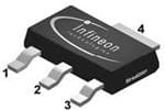
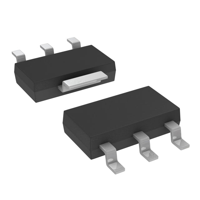
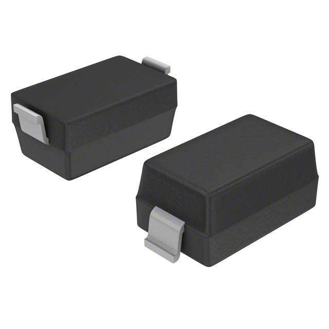
| 描述 | IC SWITCH POWER HISIDE SOT223-4电源开关 IC - 配电 SMART HI SIDE SWITCH |
| 产品分类 | PMIC - MOSFET,电桥驱动器 - 内部开关集成电路 - IC |
| 品牌 | Infineon Technologies |
| 产品手册 | http://www.infineon.com/dgdl/BSP452.pdf?folderId=db3a304314dca389011537739e37155f&fileId=db3a30431b3e89eb011b7eac4d321531&sId=db3a304339dcf4b1013a02a53068586c |
| 产品图片 |
|
| rohs | 符合RoHS无铅 / 符合限制有害物质指令(RoHS)规范要求 |
| 产品系列 | 开关 IC,电源开关 IC - 配电,Infineon Technologies BSP452miniPROFET® |
| 数据手册 | http://www.infineon.com/dgdl/Infineon-BSP452-DS-v01_00-en.pdf?folderId=db3a304314dca389011537739e37155f&fileId=db3a30431b3e89eb011b7eac4d321531&ack=t |
| 产品型号 | BSP452 |
| 产品目录页面 | |
| 产品种类 | 电源开关 IC - 配电 |
| 供应商器件封装 | PG-SOT223-4 |
| 其它名称 | BSP452DKR |
| 包装 | Digi-Reel® |
| 商标 | Infineon Technologies |
| 安装类型 | 表面贴装 |
| 安装风格 | SMD/SMT |
| 导通电阻 | 160 毫欧 |
| 导通电阻—最大值 | 0.16 Ohms |
| 封装 | Reel |
| 封装/外壳 | TO-261-4,TO-261AA |
| 封装/箱体 | SOT-223-4 |
| 工作温度 | -40°C ~ 150°C |
| 工作电源电压 | 5 V to 34 V |
| 工厂包装数量 | 4000 |
| 最大功率耗散 | 1800 mW |
| 最大工作温度 | + 150 C |
| 最大输入电压 | 34 V |
| 最小工作温度 | - 40 C |
| 最小输入电压 | 5 V |
| 标准包装 | 1 |
| 电压-电源 | 5 V ~ 34 V |
| 电流-峰值输出 | 1.5A |
| 电流-输出/通道 | 700mA |
| 电源电流—最大值 | 1 mA |
| 空闲时间—最大值 | 150 uS |
| 类型 | 高端 |
| 系列 | BSP452 |
| 输入类型 | 非反相 |
| 输出数 | 1 |
| 输出电流 | 0.7 A |
| 输出端数量 | 1 Output |
| 运行时间—最大值 | 100 uS |
| 零件号别名 | BSP452HUMA1 SP000272112 |


(SN)(P).jpg)


- 商务部:美国ITC正式对集成电路等产品启动337调查
- 曝三星4nm工艺存在良率问题 高通将骁龙8 Gen1或转产台积电
- 太阳诱电将投资9.5亿元在常州建新厂生产MLCC 预计2023年完工
- 英特尔发布欧洲新工厂建设计划 深化IDM 2.0 战略
- 台积电先进制程称霸业界 有大客户加持明年业绩稳了
- 达到5530亿美元!SIA预计今年全球半导体销售额将创下新高
- 英特尔拟将自动驾驶子公司Mobileye上市 估值或超500亿美元
- 三星加码芯片和SET,合并消费电子和移动部门,撤换高东真等 CEO
- 三星电子宣布重大人事变动 还合并消费电子和移动部门
- 海关总署:前11个月进口集成电路产品价值2.52万亿元 增长14.8%


PDF Datasheet 数据手册内容提取
Smart High-Side Power Switch BSP452 • High-side switch • Short-circuit protection SOT-223 • Input protection • Overtemperature protection with hysteresis • Overload protection • Overvoltage protection • Switching inductive load • Clamp of negative output voltage with inductive loads • Undervoltage shutdown 1 • Maximum current internally limited SOT-223 •Electrostatic discharge (ESD) protection • Reverse battery protection1) PG-SOT-223 • AEC qualified •PacGkaregeen: p rSoOduTc t2 (2R3oHS compliant) Type Ordering code BSP 452 Q67000-S271 Application •µC compatible power switch for 12 V DC grounded loads • All types of resistive, inductive and capacitive loads • Replaces electromechanical relays and discrete circuits General Description N channel vertical power FET with charge pump, ground referenced CMOS compatible input,monolithically integrated in Smart SIPMOS technology. Fully protected by embedded protection functions. Blockdiagramm: + Vbb 4 Voltage Overvoltage Current Gate source protection limit protection ESD- VLogic Diode Voltage Charge pump Limit for OUT unclamped 1 sensor Level shifter ind. loads Temperature sensor Rectifier R 3 IN in Load ESD Logic GND miniPROFET 2 Signal GND Load GND 1) With resistor RGND=150Ω in GND connection, resistor in series with IN connections reverse load current limited by connected load. Data Sheet 1 V1.0, 2007-05-25
Smart High-Side Power Switch BSP452 Pin Symbol Function 1 OUT O Output to the load 2 GND - Logic ground 3 IN I Input, activates the power switch in case of logical high signal 4 Vbb + Positive power supply voltage Maximum Ratings at Tj = 25 °C unless otherwise specified Parameter Symbol Values Unit Supply voltage V 40 V bb Load current self-limited I I A L L(SC) Maximum input voltage2) V -5.0...V V IN bb Maximum input current I ±5 mA IN Inductive load switch-off energy dissipation, E 0.5 J AS single pulse I = 0.5A , T = 150°C L A (not tested, specified by design) Load dump protection3)VLoadDump=UA+Vs RL= 24Ω VLoad dump4) 60 V R=2Ω , t=400ms, IN= low or high, U =13,5V R= 80Ω 80 I d A L (not tested, specified by design) Electrostatic discharge capability (ESD)5) PIN 3 V ±1 kV ESD PIN 1,2,4 ±2 Operating temperature range T -40 ...+150 °C j Storage temperature range T -55 ...+150 stg Max. power dissipation (DC)6) T = 25 °C P 1.8 W A tot Thermal resistance chip - soldering point: R 7 K/W thJS chip - ambient:6) R 70 thJA 2) At VIN > Vbb, the input current is not allowed to exceed ±5 mA. 3) Supply voltages higher than Vbb(AZ) require an external current limit for the GND pin, e.g. with a 150 Ω resistor in the GND connection A resistor for the protection of the input is integrated. 4) VLoad dump is setup without the DUT connected to the generator per ISO 7637-1 and DIN 40839 5) HBM according to MIL-STD 883D, Methode 3015.7 6)BSP 452 on epoxy pcb 40 mm x 40 mm x 1.5 mm with 6 cm2 copper area for Vbb connection Data Sheet 2 V1.0, 2007-05-25
Smart High-Side Power Switch BSP452 Electrical Characteristics Parameter and Conditions Symbol Values Unit atTj = 25 °C,Vbb = 13.5V unless otherwise specified min typ max Load Switching Capabilities and Characteristics On-state resistance (pin 4 to 1) IL = 0.5 A, Vin = high Tj = 25°C RON -- 0.16 0.2 Ω Tj = 150°C -- -- 0.4 Nominal load current (pin 4 to 1)7) I 0.7 -- -- A L(ISO) ISO Standard: V = V -V = 0.5 V ON bb OUT T = 85 °C S Turn-on time to 90% V t -- 60 100 µs OUT on Turn-off time to 10% V t -- 60 150 OUT off R = 24 Ω L Slew rate on dV/dt -- 2 4 V/µs on 10 to 30% V ,R = 24 Ω OUT L Slew rate off -dV/dt -- 2 4 V/µs off 70 to 40% V ,R = 24 Ω OUT L Input Allowable input voltage range, (pin 3 to 2) V -3.0 -- V V IN bb Input turn-on threshold voltage V -- -- 3.5 V IN(T+) Tj = -40...+150°C Input turn-off threshold voltage V 1.5 -- -- V IN(T-) Tj = -40...+150°C Input threshold hysteresis ∆V -- 0.5 -- V IN(T) Off state input current (pin 3) V = 1.2 V I 10 -- 60 µA IN(off) IN(off) Tj = -40...+150°C On state input current (pin 3) V = 3.0 V to V I 10 -- 100 µA IN(on) bb IN(on) Tj = -40...+150°C Input resistance R 1.5 2.8 3.5 kΩ IN 7)IL(ISO) is limited by current limitation, see IL(SC), next page Data Sheet 3 V1.0, 2007-05-25
Smart High-Side Power Switch BSP452 Parameter and Conditions Symbol Values Unit atTj = 25 °C,Vbb = 13.5V unless otherwise specified min typ max Operating Parameters Operating voltage8) Tj =-40...+150°C Vbb(on) 5.0 -- 34 V Undervoltage shutdown Tj =-40...+150°C Vbb(under) 3.5 -- 5 V Undervoltage restart Tj =-40...+25°C Vbb(u rst) -- -- 6.5 V Tj =+150°C 7.0 Undervoltage restart of charge pumpe V -- 5.6 7 V bb(ucp) see diagram page 77 Undervoltage hysteresis ∆V -- 0.3 -- V bb(under) ∆V = V - V bb(under) bb(u rst) bb(under) Overvoltage shutdown Tj =-40...+150°C Vbb(over) 34 -- 42 V Overvoltage restart Tj =-40...+150°C Vbb(o rst) 33 -- -- V Overvoltage hysteresis Tj =-40...+150°C ∆Vbb(over) -- 0.7 -- V Standby current (pin 4), Vin = low Tj =-40...+150°C Ibb(off) -- 10 25 µA Operating current (pin 2), V = 5 V I -- 1 1.6 mA in GND leakage current (pin 1) Vin = low Tj =-40...+25°C IL(off) -- 2 5 µA Tj =150 °C 7 Protection Functions Current limit (pin 4 to 1) Tj = 25°C IL(SC) 0.7 1.5 2 A Vbb = 20V Tj = -40...+150°C 0.7 -- 2.4 Overvoltage protection Ibb=4mA Tj =-40...+150°C Vbb(AZ) 41 -- -- V Output clamp (ind. load switch off) V 41 47 -- V ON(CL) atV =V -V I = 4mA OUT bb ON(CL), bb Thermal overload trip temperature T 150 -- -- °C jt Thermal hysteresis ∆T -- 10 -- K jt Inductive load switch-off energy dissipation9) E -- -- 0.5 J AS T = 150 °C, single pulse, I = 0.5 A, V = 12 V j Start L bb (not tested, specified by design) Reverse battery (pin 4 to 2) 10) -V -- -- 30 V bb (not tested, specified by design) 8) At supply voltage increase up to Vbb= 5.6 V typ without charge pump, VOUT≈Vbb - 2 V 9) While demagnetizing load inductance, dissipated energy in PROFET is EAS=∫VON(CL) * iL(t)dt, approx. EAS=1/2*L * I2L* (VOVNO(CNL()C -L V)bb ) 10) Requires 150 Ω resistor in GND connection. Reverse load current (through intrinsic drain-source diode) is normally limited by the connected load. Data Sheet 4 V1.0, 2007-05-25
Smart High-Side Power Switch BSP452 Max. allowable power dissipation Current limit characteristic Ptot = f (TA,TSP) IL(SC) = f (Von);(Von see testcircuit) Ptot [W] IL(SC) [A] 18 2 16 1.8 1.6 14 1.4 12 150°C T SP 1.2 25°C 10 1 -40°C 8 0.8 6 0.6 4 0.4 T A 2 0.2 0 0 0 25 50 75 100 125 150 0 2 4 6 8 10 12 14 TA, TSP[°C] Von [V] On state resistance (Vbb-pin to OUT-pin) Typ. input current RON = f (Tj); Vbb = 13.5 V; IL = 0.5 A IIN = f (VIN);Vbb = 13,5 V RON [Ω] IIN [µA] 0.4 50 -40°C 45 0.35 40 +25°C 0.3 35 98% 0.25 30 +150°C 0.2 25 20 0.15 15 0.1 10 0.05 5 0 0 -50 -25 0 25 50 75 100 125 150 0 2 4 6 8 10 12 14 Tj [°C] VIN [V] Data Book 5 20 08 96 Data Sheet 5 V1.0, 2007-05-25
Smart High-Side Power Switch BSP452 Typ. operating current Typ. overload current IGND = f (Tj);Vbb = 13,5 V; VIN = high IL(lim) = f (t); Vbb = 13,5 V, no heatsink, Param.: Tjstart IGND [mA] IL(lim) [A] 0.8 1.4 0.7 1.2 0.6 1 0.5 0.8 +150°C +25°C -40°C 0.4 0.6 0.3 0.4 0.2 0.1 0.2 0 0 -50 -25 0 25 50 75 100 125 150 -50 0 50 100 150 200 250 300 350 400 Tj [°C] t [ms] Typ. standby current Short circuit current Ibb(off) = f (Tj);Vbb = 13,5 V;VIN = low IL(SC) = f (Tj);Vbb = 13,5 V Ibb(off) [µA] IL(SC) [A] 8 1.4 7 1.2 6 1 5 0.8 4 0.6 3 0.4 2 0.2 1 0 0 -50 -25 0 25 50 75 100 125 150 -50 -25 0 25 50 75 100 125 150 Tj [°C] Tj [°C] Data Sheet 6 V1.0, 2007-05-25
Smart High-Side Power Switch BSP452 Typ. input turn on voltage threshold Figure 6: Undervoltage restart of charge pumpe VIN(T+) = f (Tj); VIN(T+) [V] VON [V] 3 13V 2.5 2 V 1.5 bb(over) V bb(o rst) 1 V bb(u rst) 0.5 V bb(u cp) V bb(under) 0 -50 -25 0 25 50 75 100 125 150 Vbb [V] Tj [°C] charge pump starts at Vbb(ucp) about 7 V typ. Typ. on-state resistance (Vbb-Pin to Out-Pin) Test circuit RON = f (Vbb,IL);IL=0.5A, Tj = 25°C RON [mΩ] 300 250 200 150 100 50 0 0 5 10 15 20 25 Vbb [V] Data Sheet 7 V1.0, 2007-05-25
Smart High-Side Power Switch BSP452 Package Outlines A 6.5±0.2 1.6±0.1 3±0.1 0.1 max B 4 +0.2 acc. to max DIN 6784 7±0.3 15˚ 3.5±0.2 n mi 1 2 3 5 0. 0.7±0.1 2.3 0.28±0.04 4.6 0.25 M A 0.25 M B Figure1 PG-SOT-223 (Plastic Dual Small Outline Package) (RoHS-compliant) To meet the world-wide customer requirements for environmentally friendly products and to be compliant with government regulations the device is available as a green product. Green products are RoHS-Compliant (i.e Pb- free finish on leads and suitable for Pb-free soldering according to IPC/JEDEC J-STD-020). Please specify the package needed (e.g. green package) when placing an order You can find all of our packages, sorts of packing and others in our Infineon Internet Page “Products”: http://www.infineon.com/products. Dimensions in mm Data Sheet 8 V1.0, 2007-05-25
Smart High-Side Power Switch BSP452 Revision History Version Date Changes 1.0 2007-05-25 Creation of the green datasheet. First page : Adding the green logo and the AEC qualified Adding the bullet AEC qualified and the RoHS compliant features Package page Modification of the package to be green. Data Sheet 9 V1.0, 2007-05-25
Edition 2007-05-25 Published by Infineon Technologies AG 81726 Munich, Germany © Infineon Technologies AG 5/29/07. All Rights Reserved. Legal Disclaimer The information given in this document shall in no event be regarded as a guarantee of conditions or characteristics (“Beschaffenheitsgarantie”). With respect to any examples or hints given herein, any typical values stated herein and/or any information regarding the application of the device, Infineon Technologies hereby disclaims any and all warranties and liabilities of any kind, including without limitation warranties of non-infringement of intellectual property rights of any third party. Information For further information on technology, delivery terms and conditions and prices please contact your nearest Infineon Technologies Office (www.infineon.com). Warnings Due to technical requirements components may contain dangerous substances. For information on the types in question please contact your nearest Infineon Technologies Office. Infineon Technologies Components may only be used in life-support devices or systems with the express written approval of Infineon Technologies, if a failure of such components can reasonably be expected to cause the failure of that life-support device or system, or to affect the safety or effectiveness of that device or system. Life support devices or systems are intended to be implanted in the human body, or to support and/or maintain and sustain and/or protect human life. If they fail, it is reasonable to assume that the health of the user or other persons may be endangered.
Mouser Electronics Authorized Distributor Click to View Pricing, Inventory, Delivery & Lifecycle Information: I nfineon: BSP452 BSP452HUMA1 BSP452XT BTS40K21EJCXUMA1