 Datasheet下载
- 型号: BR93L86RFV-WE2
- 制造商: ROHM Semiconductor
- 库位|库存: xxxx|xxxx
- 要求:
| 数量阶梯 | 香港交货 | 国内含税 |
| +xxxx | $xxxx | ¥xxxx |
查看当月历史价格
查看今年历史价格
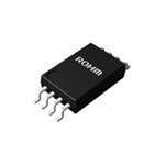
BR93L86RFV-WE2产品简介:
ICGOO电子元器件商城为您提供BR93L86RFV-WE2由ROHM Semiconductor设计生产,在icgoo商城现货销售,并且可以通过原厂、代理商等渠道进行代购。 BR93L86RFV-WE2价格参考¥1.44-¥1.68。ROHM SemiconductorBR93L86RFV-WE2封装/规格:存储器, EEPROM 存储器 IC 16Kb (1K x 16) SPI 2MHz 8-SSOPB。您可以下载BR93L86RFV-WE2参考资料、Datasheet数据手册功能说明书,资料中有BR93L86RFV-WE2 详细功能的应用电路图电压和使用方法及教程。
Rohm Semiconductor的BR93L86RFV-WE2是一款低功耗、高性能的串行SPI Flash存储器,广泛应用于各种需要高可靠性和低功耗的嵌入式系统和消费电子设备中。以下是其主要应用场景:

1. 物联网(IoT)设备:BR93L86RFV-WE2适用于各种物联网设备,如智能家居、智能穿戴设备、传感器节点等。其低功耗特性使得电池供电的设备能够长时间运行,而高速读写能力则确保了数据传输的高效性。

2. 工业自动化:在工业控制领域,该存储器可用于保存固件、配置参数和日志数据。其高可靠性和宽温度范围(-40°C至+85°C)使其能够在恶劣环境下稳定工作,确保系统的持续运行。

3. 汽车电子:这款存储器符合AEC-Q100标准,适用于汽车电子系统,如车载娱乐系统、仪表盘、ADAS(高级驾驶辅助系统)等。其高可靠性和抗干扰能力确保了车辆的安全性和稳定性。

4. 医疗设备:在医疗设备中,BR93L86RFV-WE2可以用于存储患者数据、诊断结果和设备固件。其低功耗和高可靠性特性使得它非常适合用于便携式医疗设备和远程监控系统。

5. 消费电子产品:在智能手机、平板电脑、智能音箱等消费电子产品中,该存储器可以用于存储操作系统、应用程序和用户数据。其快速读写速度和小封装尺寸有助于提高产品的性能和设计灵活性。

6. 通信设备:在路由器、交换机、基站等通信设备中,BR93L86RFV-WE2可以用于存储配置文件、固件更新和日志数据。其高可靠性和快速响应能力确保了通信系统的稳定性和安全性。

总之,BR93L86RFV-WE2凭借其低功耗、高性能和高可靠性,成为众多嵌入式系统和消费电子设备的理想选择,尤其适合对功耗和性能有严格要求的应用场景。
| 参数 | 数值 |
| 产品目录 | 集成电路 (IC) |
| 描述 | IC EEPROM 16KBIT 2MHZ 8SSOPB |
| 产品分类 | |
| 品牌 | Rohm Semiconductor |
| 数据手册 | |
| 产品图片 |
|
| 产品型号 | BR93L86RFV-WE2 |
| rohs | 无铅 / 符合限制有害物质指令(RoHS)规范要求 |
| 产品系列 | - |
| 产品培训模块 | http://www.digikey.cn/PTM/IndividualPTM.page?site=cn&lang=zhs&ptm=30341 |
| 产品目录页面 | |
| 供应商器件封装 | 8-SSOPB |
| 其它名称 | BR93L86RFV-WE2CT |
| 包装 | 剪切带 (CT) |
| 存储器类型 | EEPROM |
| 存储容量 | 16K (1K x 16) |
| 封装/外壳 | 8-LSSOP(0.173",4.40mm 宽) |
| 工作温度 | -40°C ~ 85°C |
| 接口 | Microwire 3 线串行 |
| 标准包装 | 1 |
| 格式-存储器 | EEPROMs - 串行 |
| 电压-电源 | 1.8 V ~ 5.5 V |
| 速度 | 2MHz |


- 商务部:美国ITC正式对集成电路等产品启动337调查
- 曝三星4nm工艺存在良率问题 高通将骁龙8 Gen1或转产台积电
- 太阳诱电将投资9.5亿元在常州建新厂生产MLCC 预计2023年完工
- 英特尔发布欧洲新工厂建设计划 深化IDM 2.0 战略
- 台积电先进制程称霸业界 有大客户加持明年业绩稳了
- 达到5530亿美元!SIA预计今年全球半导体销售额将创下新高
- 英特尔拟将自动驾驶子公司Mobileye上市 估值或超500亿美元
- 三星加码芯片和SET,合并消费电子和移动部门,撤换高东真等 CEO
- 三星电子宣布重大人事变动 还合并消费电子和移动部门
- 海关总署:前11个月进口集成电路产品价值2.52万亿元 增长14.8%


PDF Datasheet 数据手册内容提取
Datasheet Serial EEPROM Series Standard EEPROM Microwire BUS EEPROM(3-Wire) BR93Lxx-W ●General Description BR93Lxx-W is serial EEPROM of serial 3-line interface method ●Features ●Packages W(Typ.) x D(Typ.) x H(Max.) (cid:132) 3-line communications of chip select, serial clock, serial data input / output (the case where input and output are shared) (cid:132) Actions available at high speed 2MHz clock(2.5V to 5.5V) (cid:132) Speed write available (write time 5ms max.) (cid:132) Same package and pin layout from 1Kbit to 16Kbit (cid:132) 1.8V to 5.5V single power source action (cid:132) Address auto increment function at read action SOP8 TSSOP-B8 (cid:132) Write mistake prevention function 5.00 mm x 6.20mm x 1.71mm 3.00mm x 6.40mm x 1.20mm (cid:190) Write prohibition at power on (cid:190) Write prohibition by command code (cid:190) Write mistake prevention function at low voltage (cid:132) Program cycle auto delete and auto end function (cid:132) Program condition display by READY / BUSY (cid:132) Low current consumption SOP-J8 TSSOP-B8J (cid:190) At write action (at 5V) : 1.2mA (Typ.) 4.90mm x 6.00mm x 1.65mm 3.00mm x 4.90mm x 1.10mm (cid:190) At read action (at 5V) : 0.3mA (Typ.) (cid:190) At standby action (at 5V) : 0.1μA (Typ.)(CMOS input) (cid:132) TTL compatible( input / outputs) (cid:132) Data retention for 40 years (cid:132) Endurance up to 1,000,000 times (cid:132) Data at shipment all addresses FFFFh SSOP-B8 MSOP8 3.00mm x 6.40mm x 1.35mm 2.90mm x 4.00mm x 0.90mm DIP-T8 9.30mm x 6.50mm x 7.10mm Figure.1 ●BR93Lxx-W TSSOP- Package type SOP8 SOP-J8 SSOP-B8 TSSOP-B8 MSOP8 DIP-T8 B8J Power source Capacity Bit format Type F RF FJ RFJ FV RFV FVT RFVT RFVM RFVJ - voltage 1Kbit 64×16 BR93L46-W 1.8V to 5.5V ● ● ● ● ● ● ● ● ● ● ● 2Kbit 128×16 BR93L56-W 1.8V to 5.5V ● ● ● ● ● ● ● ● ● ● ● 4Kbit 256×16 BR93L66-W 1.8V to 5.5V ● ● ● ● ● ● ● ● ● ● ● 8Kbit 512×16 BR93L76-W 1.8V to 5.5V ● ● ● ● ● ● ● ● ● 16Kbit 1K×16 BR93L86-W 1.8V to 5.5V ● ● ● ● ● ● ● ● ● ○Product structure:Silicon monolithic integrated circuit ○This product is not designed protection against radioactive rays www.rohm.com TSZ02201-0R2R0G100390-1-2 ©2012 ROHM Co., Ltd. All rights reserved. 1/35 TSZ22111・14・001 15.Oct.2013 Rev.002
DDaattaasshheeeett BR93Lxx-W ●Absolute Maximum Ratings (Ta=25℃) Parameter Symbol Limits Unit Remarks Impressed voltage VCC -0.3 to +6.5 V 450 (SOP8) When using at Ta=25℃ or higher, 4.5mW, to be reduced per 1℃. 450 (SOP-J8) When using at Ta=25℃ or higher, 4.5mW, to be reduced per 1℃. 300 (SSOP-B8) When using at Ta=25℃ or higher, 3.0mW, to be reduced per 1℃. Permissible dissipation Pd 330 (TSSOP-B8) mW When using at Ta=25℃ or higher, 3.3mW, to be reduced per 1℃. 310 (MSOP8) When using at Ta=25℃ or higher, 3.1mW, to be reduced per 1℃. 310 (TSSOP-B8J) When using at Ta=25℃ or higher, 3.1mW, to be reduced per 1℃. 800(DIP-T8) When using at Ta=25℃ or higher, 8.0mW, to be reduced per 1℃ Storage temperature range Tstg -65 to +125 ℃ Action temperature range Topr -40 to +85 ℃ Terminal voltage ‐ -0.3 to VCC+0.3 V ●Memory Cell Characteristics(VCC=1.8V to 5.5V) Limit Parameter Unit Condition Min. Typ. Max. Endurance *1 1,000,000 - - Times Ta=25℃ Data retention *1 40 - - Years Ta=25℃ ○Shipment data all address FFFFh *1:Not 100% TESTED ●Recommended Operating Ratings Parameter Symbol Limits Unit Power source voltage VCC 1.8 to 5.5 V Input voltage VIN 0 to VCC www.rohm.com TSZ02201-0R2R0G100390-1-2 ©2012 ROHM Co., Ltd. All rights reserved. 2/35 TSZ22111・15・001 15.Oct.2013 Rev.002
DDaattaasshheeeett BR93Lxx-W ●Electrical Characteristics (Unless otherwise specified, VCC=2.5V to 5.5V, Ta=-40℃ to +85℃) Limits Parameter Symbol Unit Condition Min. Typ. Max. “L” input voltage 1 VIL1 -0.3 - 0.8 V 4.0V≦VCC≦5.5V “L” input voltage 2 VIL2 -0.3 - 0.2 x VCC V VCC≦4.0V “H” input voltage 1 VIH1 2.0 - VCC +0.3 V 4.0V≦VCC≦5.5V “H” input voltage 2 VIH2 0.7 x VCC - VCC +0.3 V VCC≦4.0V “L” output voltage 1 VOL1 0 - 0.4 V IOL=2.1mA, 4.0V≦VCC≦5.5V “L” output voltage 2 VOL2 0 - 0.2 V IOL=100μA “H” output voltage 1 VOH1 2.4 - VCC V IOH=-0.4mA, 4.0V≦VCC≦5.5V “H” output voltage 2 VOH2 VCC -0.2 - VCC V IOH=-100μA Input leak current ILI -1 - 1 µA VIN=0V to VCC Output leak current ILO -1 - 1 µA VOUT=0V to VCC, CS=0V ICC1 - - 3.0 mA fSK=2MHz, tE/W=5ms (WRITE) Current consumption ICC2 - - 1.5 mA fSK=2MHz (READ) at action ICC3 - - 4.5 mA fSK=2MHz, tE/W=5ms (WRAL, ERAL) Standby current ISB - - 2 µA CS=0V, DO=OPEN (Unless otherwise specified, VCC =1.8V to 2.5V, Ta=-40℃ to +85℃) Limits Parameter Symbol Unit Condition Min. Typ. Max. “L” input voltage VIL -0.3 - 0.2 x VCC V “H” input voltage VIH 0.7 x VCC - VCC+0.3 V “L” output voltage VOL 0 - 0.2 V IOL=100μA “H” output voltage VOH VCC-0.2 - VCC V IOH=-100μA Input leak current ILI -1 - 1 μA VIN=0V to VCC Output leak current ILO -1 - 1 μA VOUT=0V to VCC, CS=0V ICC1 - - 1.5 mA fSK=500kHz, tE/W=5ms (WRITE) Current consumption ICC2 - - 0.5 mA fSK=500kHz (READ) at action ICC3 - - 2 mA fSK=500kHz, tE/W=5ms (WRAL, ERAL) Standby current ISB - - 2 μA CS=0V, DO=OPEN www.rohm.com TSZ02201-0R2R0G100390-1-2 ©2012 ROHM Co., Ltd. All rights reserved. 3/35 TSZ22111・15・001 15.Oct.2013 Rev.002
DDaattaasshheeeett BR93Lxx-W ●Action Timing Characteristics (Ta=-40℃ to +85℃, VCC=2.5V to 5.5V) 2.5V≦VCC≦5.5V Parameter Symbol Unit Min. Typ. Max. SK frequency f - - 2 MHz SK SK “H” time t 230 - - ns SKH SK “L” time t 230 - - ns SKL CS “L” time t 200 - - ns CS CS setup time t 50 - - ns CSS DI setup time t 100 - - ns DIS CS hold time t 0 - - ns CSH DI hold time t 100 - - ns DIH Data “1” output delay time t - - 200 ns PD1 Data “0” output delay time t - - 200 ns PD0 Time from CS to output establishment t - - 150 ns SV Time from CS to High-Z t - - 150 ns DF Write cycle time t - - 5 ms E/W (Ta=-40℃ to +85℃, VCC=1.8V to 2.5V) 1.8V≦VCC≦2.5V Parameter Symbol Unit Min. Typ. Max. SK frequency f - - 500 kHz SK SK “H” time t 0.8 - - us SKH SK “L” time t 0.8 - - us SKL CS “L” time t 1 - - us CS CS setup time t 200 - - ns CSS DI setup time t 100 - - ns DIS CS hold time t 0 - - ns CSH DI hold time t 100 - - ns DIH Data “1” output delay time t - - 0.7 us PD1 Data “0” output delay time t - - 0.7 us PD0 Time from CS to output establishment t - - 0.7 us SV Time from CS to High-Z t - - 200 ns DF Write cycle time t - - 5 ms E/W ●Sync Data Input / Output Timing CS tCSS tSKH tSKL tCSH SK tDIS tDIH DI t PD0 tPD1 DO(READ) tDF DO(W RITE) STATUS VALID ○Data is taken by DI sync with the rise of SK. ○At read action, data is output from DO in sync with the rise of SK. ○The status signal at write (READY / BUSY) is output after tCS from the fall of CS after write command input, at the area DO where CS is “H”, and valid until the next command start bit is input. And, while CS is “L”, DO becomes High-Z. ○After completion of each mode execution, set CS “L” once for internal circuit reset, and execute the following action mode. www.rohm.com TSZ02201-0R2R0G100390-1-2 ©2012 ROHM Co., Ltd. All rights reserved. 4/35 TSZ22111・15・001 15.Oct.2013 Rev.002
DDaattaasshheeeett BR93Lxx-W ●Block Diagram C S Command decode Power source voltage detection Control SK Clock generation Write High voltage occurrence prohibition DI Creogmismtear nd Abudfdferer ss 6789bbbbiiiitttt Adedcdoredsesr 6789bbbbiiiitttt 12,,002448 bbiitt 10bit 10bit 4,096 bit 8,192 bit Data R/W 16,384 bit register 16bit amplifier 16bit EEPROM DO Dummy bit ●Pin Configurations TOP VIEW TOP VIEW TOP VIEW Vcc NC NC GND NC GND DO DI Vcc NC NC GND BR93LXXRF-W:SOP8 BR93LXXF-W:SOP8 BR93LXXRFJ-W:SOP-J8 BR93LXX-W:DIP-T8 BR93LXXFJ-W:SOP-J8 BR93LXXRFV-W:SSOP-B8 BR93LXXFV-W:SSOP-B8* BR93LXXRFVT-W:TSSOP-B8 BR93LXXFVT-W:TSSOP-B8* BR93LXXRFVM-W:MSOP8 BR93LXXRFVJ-W:TSSOP-B8J CS SK DI DO NC Vcc CS SK CS SK DI DO *BR93L46/56/66-W ●Pin Descriptions Pin name I / O Function VCC - Power source GND - All input / output reference voltage, 0V CS Input Chip select input SK Input Serial clock input DI Input Start bit, ope code, address, and serial data input DO Output Serial data output, READY / BUSY internal condition display output NC - Non connected terminal, Vcc, GND or OPEN www.rohm.com TSZ02201-0R2R0G100390-1-2 ©2012 ROHM Co., Ltd. All rights reserved. 5/35 TSZ22111・15・001 15.Oct.2013 Rev.002
DDaattaasshheeeett BR93Lxx-W ●Typical Performance Curves (The following characteristic data are typ. values.) Figure 2. H input voltage VIH (CS,SK,DI) Figure 3. L input voltage VIL (CS,SK,DI) Figure 4. L output voltage VOL-IOL (Vcc=1.8V) Figure 5. L output voltage VOL-IOL (Vcc=2.5V) www.rohm.com TSZ02201-0R2R0G100390-1-2 ©2012 ROHM Co., Ltd. All rights reserved. 6/35 TSZ22111・15・001 15.Oct.2013 Rev.002
DDaattaasshheeeett BR93Lxx-W ●Typical Performance Curves‐Continued Figure 6. L output voltage VOL-IOL Figure 7. H output voltage VOH-IOH (Vcc=4.0V) (Vcc=1.8V) Figure 8. H output voltage VOH-IOH (Vcc=2.5V) Figure 9. H output voltage VOH-IOH (Vcc=4.0V) www.rohm.com TSZ02201-0R2R0G100390-1-2 ©2012 ROHM Co., Ltd. All rights reserved. 7/35 TSZ22111・15・001 15.Oct.2013 Rev.002
DDaattaasshheeeett BR93Lxx-W ●Typical Performance Curves‐Continued Figure 10. Input leak current ILI (CS,SK,DI) Figure 11. Output leak current ILO (DO) Figure 13. Consumption current at READ action Figure 12. Current consumption at WRITE action ICC2 (READ, fSK=2MHz) ICC1 (WRITE, fSK=2MHz) www.rohm.com TSZ02201-0R2R0G100390-1-2 ©2012 ROHM Co., Ltd. All rights reserved. 8/35 TSZ22111・15・001 15.Oct.2013 Rev.002
DDaattaasshheeeett BR93Lxx-W ●Typical Performance Curves‐Continued Figure 14. Consumption current at WRAL action ICC3 (WRAL, fSK=2MHz) Figure 15. Current consumption at WRITE action ICC1 (WRITE, fSK=500kHz) Figure 16. Consumption current at READ action Figure 17. Consumption current at WRAL action ICC2 (READ, fSK=500kHz) ICC3 (WRAL, fSK=500kHz) www.rohm.com TSZ02201-0R2R0G100390-1-2 ©2012 ROHM Co., Ltd. All rights reserved. 9/35 TSZ22111・15・001 15.Oct.2013 Rev.002
DDaattaasshheeeett BR93Lxx-W ●Typical Performance Curves‐Continued Figure 18. Consumption current at standby action ISB Figure 19. SK frequency fSK Figure 20. SK high time tSKH Figure 21. SK low time tSKL www.rohm.com TSZ02201-0R2R0G100390-1-2 ©2012 ROHM Co., Ltd. All rights reserved. 10/35 TSZ22111・15・001 15.Oct.2013 Rev.002
DDaattaasshheeeett BR93Lxx-W ●Typical Performance Curves‐Continued Figure 22. CS low time tCS Figure 23. CS hold time tCSH Figure 24. CS setup time tCSS Figure 25. DI hold time tDIH www.rohm.com TSZ02201-0R2R0G100390-1-2 ©2012 ROHM Co., Ltd. All rights reserved. 11/35 TSZ22111・15・001 15.Oct.2013 Rev.002
DDaattaasshheeeett BR93Lxx-W ●Typical Performance Curves‐Continued Figure 26. DI setup time tDIS Figure 27. Data “0” output delay time tPD0 Figure 28. Output data “1” delay time tPD1 Figure 29. Time from CS to output establishment tSV www.rohm.com TSZ02201-0R2R0G100390-1-2 ©2012 ROHM Co., Ltd. All rights reserved. 12/35 TSZ22111・15・001 15.Oct.2013 Rev.002
DDaattaasshheeeett BR93Lxx-W ●Typical Performance Curves‐Continued Figure 30. Time from CS to High-Z tDF Figure 31. Write cycle time tE/W www.rohm.com TSZ02201-0R2R0G100390-1-2 ©2012 ROHM Co., Ltd. All rights reserved. 13/35 TSZ22111・15・001 15.Oct.2013 Rev.002
DDaattaasshheeeett BR93Lxx-W ●Description of Operations Communications of the Microwire Bus are carried out by SK (serial clock), DI (serial data input),DO (serial data output) ,and CS (chip select) for device selection. When to connect one EEPROM to a microcontroller, connect it as shown in Figure 32 (a) or Figure 32 (b). When to use the input and output common I/O port of the microcontroller, connect DI and DO via a resistor as shown in Figure 31 (b) (Refer to page 19.), and connection by 3 lines is available. In the case of plural connections, refer to Figure 32 (c). M icro- contr oller Micro- B R93LXX Micro- B R93LXX CS3 con tr oller controller CS1 CS CS CS CS CS0 SK SK SK SK SK DO DI DO DI DO DI DI DO DO CS SK DI DO CS SK DI DO CS SK DI DO Device 1 Device 2 Device 3 Figure 3 2-(a) Connection by 4 lines Figure 32-(b) Connection by 3 lines Figure 32-(c) Connection example of plural devices Figure 32. Connection method with microcontroller Communications of the Microwire Bus are started by the first “1” input after the rise of CS. This input is called a start bit. After input of the start bit, input ope code, address and data. Address and data are input all in MSB first manners. “0” input after the rise of CS to the start bit input is all ignored. Therefore, when there is limitation in the bit width of PIO of the microcontroller, input “0” before the start bit input, to control the bit width. ●Command Mode Start Ope Address Command Data bit code BR93L46-W BR93L56/66-W BR93L76/86-W *1 Read (READ) 1 10 A5,A4,A3,A2,A1,A0 A7,A6,A5,A4,A3,A2,A1,A0 A9,A8,A7,A6,A5,A4,A3,A2,A1,A0 D15 to D0(READ DATA) Write enable (WEN) 1 00 1 1 * * * * 1 1 * * * * * * 1 1 * * * * * * * * *2 Write (WRITE) 1 01 A5,A4,A3,A2,A1,A0 A7,A6,A5,A4,A3,A2,A1,A0 A9,A8,A7,A6,A5,A4,A3,A2,A1,A0 D15 to D0(WRITE DATA) *2 Write all (WRAL) 1 00 0 1 * * * * 0 1 * * * * * * 0 1 * * * * * * * * D15 to D0(WRITE DATA) Write disable (WDS) 1 00 0 0 * * * * 0 0 * * * * * * 0 0 * * * * * * * * Erase (ERASE) 1 11 A5,A4,A3,A2,A1,A0 A7,A6,A5,A4,A3,A2,A1,A0 A9,A8,A7,A6,A5,A4,A3,A2,A1,A0 Chip erase (ERAL) 1 00 1 0 * * * * 1 0 * * * * * * 1 0 * * * * * * * * ・ Input the address and the data in MSB first manners. A7 of BR93L56-W becomes Don't Care. ・ As for *, input either VIH or VIL. A9 of BR93L76-W becomes Don't Care. *Start bit Acceptance of all the commands of this IC starts at recognition of the start bit. The start bit means the first “1” input after the rise of CS. *1 As for read, by continuous SK clock input after setting the read command, data output of the set address starts, and address data in significant order are sequentially output continuously. (Auto increment function) *2 When the read and the write all commands are executed, data written in the selected memory cell is automatically deleted, and input data is written. www.rohm.com TSZ02201-0R2R0G100390-1-2 ©2012 ROHM Co., Ltd. All rights reserved. 14/35 TSZ22111・15・001 15.Oct.2013 Rev.002
DDaattaasshheeeett BR93Lxx-W ●Timing Chart 1) Read cycle (READ) ~~ ~~ ~~ CS SK *11 2 4 ~ ~ ~ ~ n n+1 ~ ~ BBBRRR999333LLL456666---WWW : n=:2 n5=, 2m7=, 5m =7 ~~ D I 1 1 0 Am A1 A0 BR93L76-W : n=29, m=9 ~~ BR93L86-W ~~ *2 ~~ DO High-Z ~ ~ 0 D15 D14 ~ ~ D1 D 0 D15 D14 ~ ~ *1 Start bit When data “1” is input for the first time after the rise of CS, this is recognized as a start bit. And when “1” is input after plural “0” are input, it is recognized as a start bit, and the following operation is started. This is common to all the commands to described hereafter. Figure 33. Read cycle ○When the read command is recognized, input address data (16bit) is output to serial. And at that moment, at taking A0, in sync with the rise of SK, “0” (dummy bit) is output. And, the following data is output in sync with the rise of SK. This IC has an address auto increment function valid only at read command. This is the function where after the above read execution, by continuously inputting SK clock, the above address data is read sequentially. And, during the auto increment, keep CS at “H”. 2) Write cycle (WRITE) CS ~ ~ ~ ~ tCS ~ ~ STATUS SK 1 2 4 ~ ~ ~ ~ n ~ ~ BR93L46-W : n=25, m=5 ~~ BR93L56-W : n=27, m=7 ~~ ~~ BR93L66-W DI 1 0 1 Am A1 A0 D15 D14 D1 D 0 BR93L76-W : n=29, m=9 ~ ~ ~ ~ ~ t~S V BR93L86-W DO BUSY READY High-Z ~ ~ tE/W Figure 34. Write cycle ○In this command, input 16bit data (D15 to D0) are written to designated addresses (Am to A0). The actual write starts by the fall of CS of D0 taken SK clock. When STATUS is not detected, (CS=”L” fixed) Max. 5ms in conformity with tE/W, and when STATUS is detected (CS=”H”), all commands are not accepted for areas where “L” (BUSY) is output from D0, therefore, do not input any command. 3) Write all cycyle (WRAL) CS ~ ~ ~ ~ tCS ~ ~ STATUS SK 1 2 5 ~ ~ ~ ~ n ~ ~ BR93L46-W : n=25 ~~ BR93L56-W ~~ ~~ : n=27 DI 1 0 0 0 1 ~ ~ D15 D14 ~ ~ D1 D 0 ~t ~S V BBBRRR999333LLL678666---WWW : n=29 DO High-Z ~ ~ ~ ~ B~U ~ SY READY Figure 35. Write all cycle tE/W ○In this command, input 16bit data is written simultaneously to all adresses. Data is not written continuously per one word but is written in bulk, the write time is only Max. 5ms in conformity with tE/W. www.rohm.com TSZ02201-0R2R0G100390-1-2 ©2012 ROHM Co., Ltd. All rights reserved. 15/35 TSZ22111・15・001 15.Oct.2013 Rev.002
DDaattaasshheeeett BR93Lxx-W 4) Write enable (WEN) / disable (WDS) cycle ~~ CS SK 1 2 3 4 5 6 7 8 n BR93L46-W : n=9 ~ ~ BR93L56-W DEINSAABBLLEE==10 10 BR93L66-W : n=11 ~~ BR93L76-W DI 1 0 0 BR93L86-W : n=13 ~~ DO High-Z Figure 36. Write enable (WEN) / disable (WDS) cycle ○ At power on, this IC is in write disable status by the internal RESET circuit. Before executing the write command, it is necessary to execute the write enable command. And, once this command is executed, it is valid unitl the write disable command is executed or the power is turned off. However, the read command is valid irrespective of write enable / diable command. Input to SK after 6 clocks of this command is available by either “H” or “L”, but be sure to input it. ○ When the write enable command is executed after power on, write enable status gets in. When the write disable command is executed then, the IC gets in write disable status as same as at power on, and then the write command is canceled thereafter in software manner. However, the read command is executable. In write enable status, even when the write command is input by mistake, write is started. To prevent such a mistake, it is recommended to execute the write disable command after completion of write. 5) Erase cycle timing (ERASE) ~~ ~~ CS tCS STATUS ~~ ~~ ~~ ~ ~ BR93L46-W : n=9, m=5 SK 1 2 4 n ~ ~ BBRR9933LL5666--WW : n=11, m=7 DI 1 1 1 Am ~ ~ A3 A2 A1 A0 ~ ~ BBRR9933LL7866--WW : n=13, m=9 ~~ ~~ ~~ t S V DO ~ ~ BUSY READY ~ ~ High-Z ~ ~ tE/W Figure 37. Erase cycle timing ○In this command, data of the designated address is made into “1”. The data of the designated address becomes “FFFFh”. Actual ERASE starts at the fall of CS after the fall of A0 taken SK clock. In ERASE, status can be detected in the same manner as in WRITE command. 6) Chip erase cycle timing (ERAL) ~~ ~~ CS tCS STATUS ~~ SK 1 2 4 ~ ~ n ~~ ~~ ~~ ~~ BBBRRR999333LLL456666---WWW : n=:9 n =11 DI 1 0 0 1 0 ~ ~ tSV ~ ~ BBRR9933LL7866--WW : n=13 DO BUSY READY ~ ~ High-Z ~ ~ tE/W Figure 38. Chip erase cycle timing ○In this command, data of all addresses is erased. Data of all addresses becomes ”FFFFh”. Actual ERASE starts at the fall of CS after the falll of the n-th clock from the start bit input. In ERAL, status can be detected in the same manner as in WRITE command. www.rohm.com TSZ02201-0R2R0G100390-1-2 ©2012 ROHM Co., Ltd. All rights reserved. 16/35 TSZ22111・15・001 15.Oct.2013 Rev.002
DDaattaasshheeeett BR93Lxx-W ●Application 1) Method to cancel each command ○READ Start bit Ope code Address*1 Data (In the case of BR93L46-W) 1bit 2bit 6bit 16bit Cancel is available in all areas in read mode. *1 Address is 8 bits in BR93L56-W, BR93L-66W ・Method to cancel:cancel by CS=“L” Address is 10 bits in BR93L76-W, BR93L86-W Figure 39. READ cancel available timing ○WRITE, WRAL ・ 25 Rise of clock *2 SK 24 25 DI D1 D0 Enlarged figure Start bit Ope code Address *1 Data tE/W (In the case of BR93L46-W) 1bit 2bit 6bit 16bit a b a:From start bit to 25 clock rise*2 *1 Address is 8 bits in BR93L56-W, BR93L66-W Cancel by CS=“L” Address is 10 bits in BR93L76-W BR93L86-W *2 27 clocks in BR93L56-W, BR93L66-W b:25 clock rise and after*2 29 clocks in BR93L76-W BR93L86-W Cancellation is not available by any means. If Vcc is made OFF in this area, designated address data is not guaranteed, therefore write once again. And when SK clock is input continuously, cancellation is not available. 29 Rise of clock *2 SK 28 29 30 31 DI D1 D0 a b c Enlarged figure *1 (In the case of BR93L86-W) 1bit 2bit 10bit 16bit a b c a:From start bit to 29 clock rise Cancel by CS=“L” b:29 clock rise and after Cancellation is not available by any means. If Vcc is made OFF in this area, Note 1) If Vcc is made OFF in this area, designated address data is designated address data is not guaranteed, therefore write once again. not guaranteed, therefore write once again. c:30 clock rise and after Note 2) If CS is started at the same timing as that of the SK rise, Cancel by CS=“L” write execution/cancel becomes unstable, therefore, it is However, when write is started in b area (CS is ended), cancellation is not recommended to fail in SK=”L” area. available by any means. As for SK rise, recommend timing of tCSS/tCSH or higher. And when SK clock is output continuously is not available. Figure 40. WRITE, WRAL cancel available timing www.rohm.com TSZ02201-0R2R0G100390-1-2 ©2012 ROHM Co., Ltd. All rights reserved. 17/35 TSZ22111・15・001 15.Oct.2013 Rev.002
DDaattaasshheeeett BR93Lxx-W ○ERASE, ERAL 9 Rise of clock*2 SK 8 9 DI A1 A0 Enlarged figure *1 1/2 Start bit Ope code Address tE/W (In the case of BR93L46-W) 1bit 2bit 6bit a b a:From start bit to 9 clock rise*2 *1 Address is 8 bits in BR93L56-W, BR93L66-W Address is 10 bits in BR93L76-W Cancel by CS=“L” b:9 clock rise and after*2 *2 11 clocks in BR93L56-W, BR93L66-W Cancellation is not available by any means. If Vcc is made OFF in this area, 13 clocks in BR93L76-W designated address data is not guaranteed, therefore write once again. And when SK clock is input continuously, cancellation is not available. 13 Rise of clock *2 SK 12 13 14 15 DI D1 a b c Enlarged figure Start bit Ope code Address*1 tE/W (In the case of BR93L86-W) 1bit 2bit 10bit a b c a:From start bit to 13 clock rise Cancel by CS=“L” b:13 clock rise and after Cancellation is not available by any means. If Vcc is made OFF in this area, designated address data is not guaranteed, therefore write once again. Note 1) If Vcc is made OFF in this area, designated address data is not guaranteed, therefore write once again. c:14 clock rise and after Cancel by CS=“L” Note 2) If CS is started at the same timing as that of the SK rise, However, when write is started in b area (CS is ended), cancellation is not write execution/cancel becomes unstable, therefore, it is available by any means. recommended to fail in SK=”L” area. And when SK clock is output continuously is not available. As for SK rise, recommend timing of tCSS/tCSH or higher. Figure 41. ERASE, ERAL cancel available timing 2) At standby ○Standby current When CS is “L”, SK input is “L”, DI input is “H”, and even with middle electric potential, current does not increase. ○Timing As shown in Figure 42, when SK at standby is “H”, if CS is started, DI status may be read at the rise edge. At standby and at power ON/OFF, when to start CS, set SK input or DI input to “L” status. (Refer to Figure 42) CS=SK=DI=”H” If CS is started when SK=”L” or DI=”L”, a start Wrong recognition as a start bit bit is recognized correctly. CS Start bit input CS Start bit input SK SK DI DI Figure 42. Wrong action timing Figure 43. Normal action timing www.rohm.com TSZ02201-0R2R0G100390-1-2 ©2012 ROHM Co., Ltd. All rights reserved. 18/35 TSZ22111・15・001 15.Oct.2013 Rev.002
DDaattaasshheeeett BR93Lxx-W 3) Equivalent circuit Output circuit Input citcuit RESET int. CS CSint. DO OEint. Figure 44. Output circuit (DO) Figure 45. Input circuit (CS) Input circuit Input circuit CS int. CS int. DI SK Figure 46. Input circuit (DI) Figure 47. Input circuit (SK) 4) I/O peripheral circuit 4-1) Pull down CS. By making CS=“L” at power ON/OFF, mistake in operation and mistake write are prevented. ○Pull down resistance Rpd of CS pin To prevent mistake in operation and mistake write at power ON/OFF, CS pull down resistance is necessary. Select an appropriate value to this resistance value from microcontroller VOH, IOH, and VIL characteristics of this IC. VOHM Rpd ≧ ・・・① IOHM VOHM ≧ VIHE ・・・② Microcontroller EEPROM Example) When V =5V, VIHE=2V, VOHM=2.4V, IOHM=2mA, CC VOHM VIHE from the equation ①, 2.4 Rpd ≧ “H” output IOHM Rpd “L” input 2×10⁻³ ∴ Rpd ≧ 1.2 [kΩ] With the value of Rpd to satisfy the above equation, VOHM becomes 2.4V or higher, and VIHE (=2.0V), the equation ② is also satisfied. Figure 48. CS pull down resistance ・VIHE : EEPROM VIH specifications ・VOHM : Microcontroller VOH specifications ・IOHM : Microcontroller IOH specifications 4-2) DO is available in both pull up and pull down. Do output become “High-Z” in other READY / BUSY output timing than after data output at read command and write command. When malfunction occurs at “High-Z” input of the microcontroller port connected to DO, it is necessary to pull down and pull up DO. When there is no influence upon the microcontroller actions, DO may be OPEN. If DO is OPEN, and at timing to output status READY, at timing of CS=“H”, SK=“H”, DI=“H”, EEPROM recognizes this as a start bit, resets READY output, and DO=”High-Z”, therefore, READY signal cannot be detected. To avoid such output, pull up DO pin for improvement. CS CS “H” SK SK Enlarged D0 DI DI High-Z READY High-Z CS=SK=DI=”H” DO DO BUSY When DO=OPEN BUSY Improvement by DO pull up DO READY CS=SK=DI=”H” BUSY When DO=pull up Figure 49. READY output timing at DO=OPEN www.rohm.com TSZ02201-0R2R0G100390-1-2 ©2012 ROHM Co., Ltd. All rights reserved. 19/35 TSZ22111・15・001 15.Oct.2013 Rev.002
DDaattaasshheeeett BR93Lxx-W ○Pull up resistance Rpu and pull down resistance Rpd of DO pin As for pull up and pull down resistance value, select an appropriate value to this resistance value from microcontroller VIH, VIL, and VOH, IOH, VOL, IOL characteristics of this IC. Vcc-VOLE Mic rocontroller EEPROM Rpu ≧ I OL E ・・・③ VILM Rpu IOLE VOLE ≦ VILM ・・・④ VOLE Example) When VCC =5V, VOLE=0.4V, IOLE=2.1mA, VILM=0.8V, from the equation ③, “L” input 5-0.4 Rpu ≧ 2.1×10⁻³ “L” output ∴ Rpu ≧ 2.2 [kΩ] With the value of Rpu to satisfy the above equation, VOLE becomes 0.4V or below, and with VILM(=0.8V), the equation ④ is also satisfied. Figure 50. DO pull up resistance ・VOLE : EEPROM VOL specifications ・IOLE : EEPROM IOL specifications ・VILM : Microcontroller VIL specifications VOHE Rpd ≧ ・・・⑤ EEPROM IOHE Microcontroller VOHE ≧ VIHM ・・・⑥ VIHM VOHE Example) When VCC =5V, VOHE=Vcc-0.2V, IOHE=0.1mA, VIHM=Vcc×0.7V from the equation ⑤, “H” input Rpd IOHE “H” output 5-0.2 Rpd ≧ 0.1×10⁻³ ∴ Rpd ≧ 48 [kΩ] With the value of Rpd to satisfy the above equation, VOHE becomes 2.4V Figure 51. DO pull down resistance or below, and with VIHM (=3.5V), the equation ⑥ is also satisfied. ・VOHE : EEPROM VOH specifications ・IOHE : EEPROM IOH specifications ・VIHM : Microcontroller VIH specifications 5) READY / BUSY status display (DO terminal) (common to BR93L46-W,BR93L56-W, BR93L66-W, BR93L76-W, BR93L86-W) This display outputs the internal status signal. When CS is started after tCS (Min.200ns) from CS fall after write command input, “H” or “L” is output. R/B display=“L” (BUSY) = write under execution ( D O s t at u s) After the timer circuit in the IC works and creates the period of tE/W, this time circuit completes automatically. And write to the memory cell is made in the period of tE/W, and during this period, other command is not accepted. R/B display = “H” (READY) = command wait status ( D O st a tu s ) Even after tE/W (max.5ms) from write of the memory cell, the following command is accepted. Therefore, CS=“H” in the period of tE/W, and when input is in SK, DI, malfunction may occur, therefore, DI=“L” in the area CS=“H”. (Especially, in the case of shared input port, attention is required.) *Do not input any command while status signal is output. Command input in BUSY area is cancelled, but command input in READY area is accepted. Therefore, status READY output is cancelled, and malfunction and mistake write may be made. CS STATUS SK CLOCK DI WINRSTITREU CTION High-Z tSV DO READY BUSY Figure 52. R/B status output timing chart www.rohm.com TSZ02201-0R2R0G100390-1-2 ©2012 ROHM Co., Ltd. All rights reserved. 20/35 TSZ22111・15・001 15.Oct.2013 Rev.002
DDaattaasshheeeett BR93Lxx-W 6) When to directly connect DI and DO This IC has independent input terminal DI and output terminal DO, and separate signals are handled on timing chart, meanwhile, by inserting a resistance R between these DI and DO terminals, it is possible to carry out control by 1 control line. Microcontroller EEPROM DI/O PORT DI R DO Figure 53. DI, DO control line common connection ○Data collision of microcontroller DI/O output and DO output and feedback of DO output to DI input. Drive from the microcontroller DI/O output to DI input on I/O timing, and signal output from DO output occur at the same time in the following points. (1) 1 clock cycle to take in A0 address data at read command Dummy bit “0” is output to DO terminal. →When address data A0 = “1” input, through current route occurs. E EPROM CS input “H” EEPROM SK input EEPROM DI input A1 A0 Collision of DI input and DO output EEPROM DO output 0 D15 D14 D13 High-Z Microcontroller DI/O port A1 A0 High-Z Microcontroller output Microcontroller input Figure 54. Collision timing at read data output at DI, DO direct connection (2) Timing of CS = “H” after write command. DO terminal in READY / BUSY function output. When the next start bit input is recognized, “HIGH-Z” gets in. →Especially, at command input after write, when CS input is started with microcontroller DI/O output “L”, READY output “H” is output from DO terminal, and through current route occurs. Feedback input at timing of these (1) and (2) does not cause disorder in basic operations, if resistance R is inserted. ~~ E EPROM CS input Write command ~ ~ ~~ EEPROM SK input Write command ~ ~ ~~ EEPROM DI input Write command ~~ E EPROM DO output Write command BU~ ~ SY READY ~ ~ READCYo llision of DHI iignhp-uZt and DO output Microcontroller DI/O port Write command B~U ~ SY READY ~ ~ Microcontroller output Microcontroller input Microcontroller output Figure 55. Collision timing at DI, DO direct connection Note) As for the case (2), attention must be paid to the following. When status READY is output, DO and DI are shared, DI=”H” and the microcontroller DI/O=”High-Z” or the microcontroller DI/O=”H”,if SK clock is input, DO output is input to DI and is recognized as a start bit, and malfunction may occur. As a method to avoid malfunction, at status READY output, set SK=“L”, or start CS within 4 clocks after “H” of READY signal is output. CS Start bit SK Because DI=”H”, set SK=”L” at CS rise. DI READY DO High-Z Figure 56. Start bit input timing at DI, DO direct connection www.rohm.com TSZ02201-0R2R0G100390-1-2 ©2012 ROHM Co., Ltd. All rights reserved. 21/35 TSZ22111・15・001 15.Oct.2013 Rev.002
DDaattaasshheeeett BR93Lxx-W ○Selection of resistance value R The resistance R becomes through current limit resistance at data collision. When through current flows, noises of power source line and instantaneous stop of power source may occur. When allowable through current is defined as I, the following relation should be satisfied. Determine allowable current amount in consideration of impedance and so forth of power source line in set. And insert resistance R, and set the value R to satisfy EEPROM input level VIH/VIL even under influence of voltage decline owing to leak current and so forth. Insertion of R will not cause any influence upon basic operations. (1) Address data A0 = “1” input, dummy bit “0” output timing (When microcontroller DI/O output is “H”, EEPROM DO outputs “L”, and “H” is input to DI) ・Make the through current to EEPROM 10mA or below. ・See to it that the level VIH of EEPROM should satisfy the following. Conditions VOHM ≦ VIHE Microcontroller EEPROM VOHM ≦ IOHM×R + VOLE DI/O PORT DI At this moment, if VOLE=0V, “H” output VOHM VOHM ≦ IOHM×R IOHM R VOHM DO ∴ R ≧ ・・・⑦ IOHM VOLE ・VIHE : EEPROM VIH specifications “L” output ・VOLE : EEPROM VOL specifications ・VOHM : Microcontroller VOH specifications ・IOHM : Microcontroller IOH specifications Figure 57. Circuit at DI, DO direct connection (Microcontroller DI/O “H” output, EEPROM “L” output) (2) DO status READY output timing (When the microcontroller DI/O is “L”, EEPROM DO output “H”, and “L” is input to DI) ・Set the EEPROM input level VIL so as to satisfy the following. Conditions Microcontroller EEPROM VOLM ≧ VILE “L” output DI/O PORT DI VOLM ≧ VOHE – IOLM×R VOLM As this moment, VOHE=Vcc IOHM R VOLM ≧ Vcc – IOLM×R DO Vcc – VOLM ∴ ・・・⑧ VOHE “H” output IOLM ・VILE : EEPROM VIL specifications ・VOHE : EEPROM VOH specifications ・VOLM : Microcontroller VOL specifications ・IOLM : Microcontroller IOL specifications Example) When Vcc=5V, VOHM=5V, IOHM=0.4mA, VOLM=5V, IOLM=0.4mA, From the equation ⑦, From the equation⑧, VOHM Vcc – VOLM R ≧ R ≧ IOHM IOLM 5 5 – 0.4 R ≧ R ≧ 0.4×10⁻³ 2.1×10⁻³ ∴ R ≧ 12.5 [kΩ] ・・・⑨ ∴ R ≧ 2.2 [kΩ] ・・・⑩ Therefore, from the equations ⑨ and ⑩, ∴ R ≧ 12.5 [kΩ] Figure 58. Circuit at DI, DO direct connection (Microcontroller DI/O “L” output, EEPROM “H” output) www.rohm.com TSZ02201-0R2R0G100390-1-2 ©2012 ROHM Co., Ltd. All rights reserved. 22/35 TSZ22111・15・001 15.Oct.2013 Rev.002
DDaattaasshheeeett BR93Lxx-W 7) Notes on power ON/OFF ・At power ON/OFF, set CS “L”. When CS is “H”, this IC gets in input accept status (active). If power is turned on in this status, noises and the likes may cause malfunction, mistake write or so. To prevent these, at power ON, set CS “L”. (When CS is in “L” status, all inputs are cancelled.) And at power decline, owing to power line capacity and so forth, low power status may continue long. At this case too, owing to the same reason, malfunction, mistake write may occur, therefore, at power OFF too, set CS “L”. VCC VCC GND VCC CS GND Figure 59. Timing at power ON/OFF (Bad example)CS pin is pulled up to Vcc. Bad example Good examp(le Good example)It is “L” at power ON/OFF. In this case, CS becomes “H” (active status), and EEPROM may have malfunction, Set 10ms or higher to recharge at power OFF. mistake write owing to noise and the likes. When power is turned on without observing this condition, Even when CS input is High-Z, the status becomes like this case, which please note. IC internal circuit may not be reset, which please note. ○POR citcuit This IC has a POR (Power On Reset) circuit as a mistake write countermeasure. After POR action, it gets in write disable status. The POR circuit is valid only when power is ON, and does not work when power is OFF. However, if CS is “H” at power ON/OFF, it may become write enable status owing to noises and the likes. For secure actions, observe the follwing conditions. 1. Set CS=”L” 2. Turn on power so as to satisfy the recommended conditions of tR, tOFF, Vbot for POR circuit action. tR VCC Recommended conditions of tR, tOFF, Vbot tR tOFF Vbot 10ms or below 10ms or higher 0.3V or below tOFF Vbot 100ms or below 10ms or higher 0.2V or below 0 ○LVCC circuit Figure 60. Rise waveform diagram LVCC (VCC-Lockout) circuit prevents data rewrite action at low power, and prevents wrong write. At LVCC voltage (Typ.=1.2V) or below, it prevent data rewrite. 8) Noise countermeasures ○VCC noise (bypass capacitor) When noise or surge gets in the power source line, malfunction may occur, therefore, for removing these, it is recommended to attach a by pass capacitor (0.1µF) between IC VCC and GND, At that moment, attach it as close to IC as possible.And, it is also recommended to attach a bypass capacitor between board VCC and GND. ○SK noise When the rise time (tR) of SK is long, and a certain degree or more of noise exists, malfunction may occur owing to clock bit displacement. To avoid this, a Schmitt trigger circuit is built in SK input. The hysteresis width of this circuit is set about 0.2V, if noises exist at SK input, set the noise amplitude 0.2Vp-p or below. And it is recommended to set the rise time (tR) of SK 100ns or below. In the case when the rise time is 100ns or higher, take sufficient noise countermeasures. Make the clock rise, fall time as small as possible. www.rohm.com TSZ02201-0R2R0G100390-1-2 ©2012 ROHM Co., Ltd. All rights reserved. 23/35 TSZ22111・15・001 15.Oct.2013 Rev.002
DDaattaasshheeeett BR93Lxx-W ●Notes for Use (1) Described numeric values and data are design representative values, and the values are not guaranteed. (2) We believe that application circuit examples are recommendable, however, in actual use, confirm characteristics further sufficiently. In the case of use by changing the fixed number of external parts, make your decision with sufficient margin in consideration of static characteristics and transition characteristics and fluctuations of external parts and our IC. (3) Absolute Maximum Ratings If the absolute maximum ratings such as impressed voltage and action temperature range and so forth are exceeded, IC may be destructed. Do not impress voltage and temperature exceeding the absolute maximum ratings. In the case of fear exceeding the absolute maximum ratings, take physical safety countermeasures such as fuses, and see to it that conditions exceeding the absolute maximum ratings should not be impressed to IC. (4) GND electric potential Set the voltage of GND terminal lowest at any action condition. Make sure that each terminal voltage is not lower than that of GND terminal in consideration of transition status. (5) Heat design In consideration of allowable loss in actual use condition, carry out heat design with sufficient margin. (6) Terminal to terminal shortcircuit and wrong packaging When to package IC onto a board, pay sufficient attention to IC direction and displacement. Wrong packaging may destruct IC. And in the case of shortcircuit between IC terminals and terminals and power source, terminal and GND owing to foreign matter, IC may be destructed. (7) Use in a strong electromagnetic field may cause malfunction, therefore, evaluate design sufficiently Status of this document The Japanese version of this document is formal specification. A customer may use this translation version only for a reference to help reading the formal version. If there are any differences in translation version of this document formal version takes priority. www.rohm.com TSZ02201-0R2R0G100390-1-2 ©2012 ROHM Co., Ltd. All rights reserved. 24/35 TSZ22111・15・001 15.Oct.2013 Rev.002
DDaattaasshheeeett BR93Lxx-W ●Ordering Information Product Code Description B R 9 3 L x x x x - W x x BUS Type 93:Microwire Operating temperature -40℃ to +85℃ Capacity 46=1K 76=8K 56=2K 86=16K 66=4K Package type F, RF : SOP8 FJ, RFJ : SOP-J8 FV, RFV : SSOP-B8 FVT, RFVT : TSSOP-B8 RFVJ : TSSOP-B8J RFVM : MSOP8 Blank : DIP-T8 Double cell Package specifications E2 :reel shape emboss taping TR :reel shape emboss taping www.rohm.com TSZ02201-0R2R0G100390-1-2 ©2012 ROHM Co., Ltd. All rights reserved. 25/35 TSZ22111・15・001 15.Oct.2013 Rev.002
DDaattaasshheeeett BR93Lxx-W ●Physical Dimension Tape and Reel Information S OP8 5.0±0.2 (MAX 5.35 include BURR) +6° 4°−4° 8 7 6 5 5 3 2 N 1 0. 0. MI 0. ± ± ± 2 4 3 9 6. 4. 0. 0. 1 2 3 4 0.595 +0.1 0.17 -0.05 1 . 0 ± S 5 . 1 0.1 S 1 1 . 0 1.27 0.42±0.1 (Unit : mm) <Tape and Reel information> Tape Embossed carrier tape Quantity 2500pcs E2 Direction ( The direction is the 1pin of product is at the upper left when you hold ) of feed reel on the left hand and you pull out the tape on the right hand Direction of feed 1pin Reel ∗ Order quantity needs to be multiple of the minimum quantity. www.rohm.com TSZ02201-0R2R0G100390-1-2 ©2012 ROHM Co., Ltd. All rights reserved. 26/35 TSZ22111・15・001 15.Oct.2013 Rev.002
DDaattaasshheeeett BR93Lxx-W ●Physical Dimension Tape and Reel Information - Continued SOP-J8 4.9±0.2 (MAX 5.25 include BURR) +6° 4°−4° 8 7 6 5 N 3 2 MI 0. 0. 5 ± ± 4 0 9 . 6. 3. 0 1 2 3 4 0.545 0.2±0.1 S 1 . 0 ± 5 7 3 . 1 5 1.27 7 0.42±0.1 1 . 0 0.1 S (Unit : mm) <Tape and Reel information> Tape Embossed carrier tape Quantity 2500pcs E2 Direction ( The direction is the 1pin of product is at the upper left when you hold ) of feed reel on the left hand and you pull out the tape on the right hand Direction of feed 1pin Reel ∗ Order quantity needs to be multiple of the minimum quantity. www.rohm.com TSZ02201-0R2R0G100390-1-2 ©2012 ROHM Co., Ltd. All rights reserved. 27/35 TSZ22111・15・001 15.Oct.2013 Rev.002
DDaattaasshheeeett BR93Lxx-W ●Physical Dimension Tape and Reel Information – Continued SSOP-B8 3.0±0.2 (MAX 3.35 include BURR) 8 7 6 5 32 .. 00 ±± 44 .. 64 N I M 3 . 0 1 2 3 4 1 0.15±0.1 0. ± 5 S 1 1. 0.1 S 1 +0.06 0. (0.52) 0.65 0.22−0.04 0.08 M (Unit : mm) <Tape and Reel information> Tape Embossed carrier tape Quantity 2500pcs E2 Direction ( The direction is the 1pin of product is at the upper left when you hold ) of feed reel on the left hand and you pull out the tape on the right hand Direction of feed 1pin Reel ∗ Order quantity needs to be multiple of the minimum quantity. www.rohm.com TSZ02201-0R2R0G100390-1-2 ©2012 ROHM Co., Ltd. All rights reserved. 28/35 TSZ22111・15・001 15.Oct.2013 Rev.002
DDaattaasshheeeett BR93Lxx-W ●Physical Dimension Tape and Reel Information – Continued TSSOP-B8J 3.0±0.1 (MAX 3.35 include BURR) 4 ± 4 8 7 6 5 2 1 0. 0. ± ± 9 0 4. 3. 15 . 0 ± 5 2 4 . 0 . 0 ± 5 9 . 1 2 3 4 0 1PIN MARK +0.05 X 5 0.525 0.145−0.03 A 0 . M 0 S ± 1 5 1. 8 . 5 0 0 0.08 S . 0 +0.05 ±1 0.32−0.04 0.08 M . 0 0.65 (Unit : mm) <Tape and Reel information> Tape Embossed carrier tape Quantity 2500pcs E2 Direction ( The direction is the 1pin of product is at the upper left when you hold ) of feed reel on the left hand and you pull out the tape on the right hand Direction of feed 1pin Reel ∗ Order quantity needs to be multiple of the minimum quantity. www.rohm.com TSZ02201-0R2R0G100390-1-2 ©2012 ROHM Co., Ltd. All rights reserved. 29/35 TSZ22111・15・001 15.Oct.2013 Rev.002
DDaattaasshheeeett BR93Lxx-W ●Physical Dimension Tape and Reel Information – Continued TSSOP-B8 3.0±0.1 (MAX 3.35 include BURR) 4 ± 4 8 7 6 5 2 1 . . 0 0 ± ± 4 4 6. 4. 5 1 . 0 ± 5 2 0. 0. ± 0 1 2 3 4 1. 1PIN MARK +0.05 0.525 0.145−0.03 5 X A .0 S M 0 ± 2 0 . 1 . 1 5 0 0.08 S . 0 +0.05 ±1 0.245−0.04 0.08 M . 0 0.65 (Unit : mm) <Tape and Reel information> Tape Embossed carrier tape Quantity 3000pcs E2 Direction ( The direction is the 1pin of product is at the upper left when you hold ) of feed reel on the left hand and you pull out the tape on the right hand Direction of feed 1pin Reel ∗ Order quantity needs to be multiple of the minimum quantity. www.rohm.com TSZ02201-0R2R0G100390-1-2 ©2012 ROHM Co., Ltd. All rights reserved. 30/35 TSZ22111・15・001 15.Oct.2013 Rev.002
DDaattaasshheeeett BR93Lxx-W ●Physical Dimension Tape and Reel Information – Continued MSOP8 2.9±0.1 (MAX 3.25 include BURR) + 6° 4°−4° 5 2 8 7 6 5 1 0. 0. ± ± 6 2 1 9 0. 0. 0. .2 ± ± 0 0 8 4. 2. 1 2 3 4 1PIN MARK +0.05 0.145−0.03 0.475 S X A M 9 +0.05 . 0 0.22 −0.04 5 5 0 0 . . 0 0 0.08 S ± ± 5 8 7 0 . . 0.65 0 0 (Unit : mm) <Tape and Reel information> Tape Embossed carrier tape Quantity 3000pcs TR Direction ( The direction is the 1pin of product is at the upper right when you hold ) of feed reel on the left hand and you pull out the tape on the right hand 1pin Direction of feed Reel ∗ Order quantity needs to be multiple of the minimum quantity. www.rohm.com TSZ02201-0R2R0G100390-1-2 ©2012 ROHM Co., Ltd. All rights reserved. 31/35 TSZ22111・15・001 15.Oct.2013 Rev.002
DDaattaasshheeeett BR93Lxx-W ●Physical Dimension Tape and Reel Information – Continued DIP-T8 9.3±0.3 8 5 3 . 0 ± 5 . 6 1 4 . n 7.62 Mi 1 5 3 . . 0 0 ± 4 . 3 2 . 0 ± 0.3±0.1 2 3. 0°−15° 2.54 0.5±0.1 (Unit : mm) <Tape and Reel information> Container Tube Quantity 2000pcs Direction of feed Direction of products is fixed in a container tube ∗ Order quantity needs to be multiple of the minimum quantity. www.rohm.com TSZ02201-0R2R0G100390-1-2 ©2012 ROHM Co., Ltd. All rights reserved. 32/35 TSZ22111・15・001 15.Oct.2013 Rev.002
DDaattaasshheeeett BR93Lxx-W ●Marking Diagrams SOP8(TOP VIEW) SOP-J8(TOP VIEW) Part Number Marking Part Number Marking LOT Number LOT Number 1PIN MARK 1PIN MARK SSOP-B8(TOP VIEW) TSSOP-B8J(TOP VIEW) Part Number Marking Part Number Marking LOT Number LOT Number 1PIN MARK 1PIN MARK TSSOP-B8(TOP VIEW) Part Number Marking MSOP8(TOP VIEW) Part Number Marking LOT Number LOT Number 1PIN MARK 1PIN MARK DIP-T8 (TOP VIEW) Part Number Marking LOT Number www.rohm.com TSZ02201-0R2R0G100390-1-2 ©2012 ROHM Co., Ltd. All rights reserved. 33/35 TSZ22111・15・001 15.Oct.2013 Rev.002
DDaattaasshheeeett BR93Lxx-W ●Marking Information Product Capacity Name Package Type Orderable Part Number Marking L46 BR93L46F-WE2 SOP8 RL46 BR93L46RF-WE2 L46 BR93L46FJ-WE2 SOP-J8 RL46 BR93L46RFJ-WE2 L46 BR93L46FV-WE2 SSOP-B8 1K RL46 BR93L46RFV-WE2 R46 TSSOP-B8J BR93L46RFVJ-WE2 L46 BR93L46FVT-WE2 TSSOP-B8 RL46 BR93L46RFVT-WE2 R46 MSOP8 BR93L46RFVM-WTR BR93L46 DIP-T8 BR93L46-W L56 BR93L56F-WE2 SOP8 RL56 BR93L56RF-WE2 L56 BR93L56FJ-WE2 SOP-J8 RL56 BR93L56RFJ-WE2 L56 BR93L56FV-WE2 SSOP-B8 2K RL56 BR93L56RFV-WE2 R56 TSSOP-B8J BR93L56RFVJ-WE2 L56 BR93L56FVT-WE2 TSSOP-B8 RL56 BR93L56RFVT-WE2 R56 MSOP8 BR93L56RFVM-WTR BR93L56 DIP-T8 BR93L56-W L66 BR93L66F-WE2 SOP8 RL66 BR93L66RF-WE2 L66 BR93L66FJ-WE2 SOP-J8 RL66 BR93L66RFJ-WE2 L66 BR93L66FV-WE2 SSOP-B8 4K RL66 BR93L66RFV-WE2 R66 TSSOP-B8J BR93L66RFVJ-WE2 L66 BR93L66FVT-WE2 TSSOP-B8 RL66 BR93L66RFVT-WE2 R66 MSOP8 BR93L66RFVM-WTR BR93L66 DIP-T8 BR93L66-W L76 BR93L76F-WE2 SOP8 RL76 BR93L76RF-WE2 L76 BR93L76FJ-WE2 SOP-J8 RL76 BR93L76RFJ-WE2 8K RL76 SSOP-B8 BR93L76RFV-WE2 R76 TSSOP-B8J BR93L76RFVJ-WE2 RL76 TSSOP-B8 BR93L76RFVT-WE2 R76 MSOP8 BR93L76RFVM-WTR BR93L76 DIP-T8 BR93L76-W L86 BR93L86F-WE2 SOP8 RL86 BR93L86RF-WE2 L86 BR93L86FJ-WE2 SOP-J8 RL86 BR93L86RFJ-WE2 16K RL86 SSOP-B8 BR93L86RFV-WE2 R86 TSSOP-B8J BR93L86RFVJ-WE2 RL86 TSSOP-B8 BR93L86RFVT-WE2 R86 MSOP8 BR93L86RFVM-WTR BR93L86 DIP-T8 BR93L86-W www.rohm.com TSZ02201-0R2R0G100390-1-2 ©2012 ROHM Co., Ltd. All rights reserved. 34/35 TSZ22111・15・001 15.Oct.2013 Rev.002
DDaattaasshheeeett BR93Lxx-W ●Revision History Date Revision Changes 31.Aug.2012 001 New Release 15.Oct.2013 002 Page34 Modify the Marking of MSOP8 pachage of 8K and 16K. www.rohm.com TSZ02201-0R2R0G100390-1-2 ©2012 ROHM Co., Ltd. All rights reserved. 35/35 TSZ22111・15・001 15.Oct.2013 Rev.002
DDaattaasshheeeett Notice Precaution on using ROHM Products 1. Our Products are designed and manufactured for application in ordinary electronic equipments (such as AV equipment, OA equipment, telecommunication equipment, home electronic appliances, amusement equipment, etc.). If you intend to use our Products in devices requiring extremely high reliability (such as medical equipment (Note 1), transport equipment, traffic equipment, aircraft/spacecraft, nuclear power controllers, fuel controllers, car equipment including car accessories, safety devices, etc.) and whose malfunction or failure may cause loss of human life, bodily injury or serious damage to property (“Specific Applications”), please consult with the ROHM sales representative in advance. Unless otherwise agreed in writing by ROHM in advance, ROHM shall not be in any way responsible or liable for any damages, expenses or losses incurred by you or third parties arising from the use of any ROHM’s Products for Specific Applications. (Note1) Medical Equipment Classification of the Specific Applications JAPAN USA EU CHINA CLASSⅢ CLASSⅡb CLASSⅢ CLASSⅢ CLASSⅣ CLASSⅢ 2. ROHM designs and manufactures its Products subject to strict quality control system. However, semiconductor products can fail or malfunction at a certain rate. Please be sure to implement, at your own responsibilities, adequate safety measures including but not limited to fail-safe design against the physical injury, damage to any property, which a failure or malfunction of our Products may cause. The following are examples of safety measures: [a] Installation of protection circuits or other protective devices to improve system safety [b] Installation of redundant circuits to reduce the impact of single or multiple circuit failure 3. Our Products are designed and manufactured for use under standard conditions and not under any special or extraordinary environments or conditions, as exemplified below. Accordingly, ROHM shall not be in any way responsible or liable for any damages, expenses or losses arising from the use of any ROHM’s Products under any special or extraordinary environments or conditions. If you intend to use our Products under any special or extraordinary environments or conditions (as exemplified below), your independent verification and confirmation of product performance, reliability, etc, prior to use, must be necessary: [a] Use of our Products in any types of liquid, including water, oils, chemicals, and organic solvents [b] Use of our Products outdoors or in places where the Products are exposed to direct sunlight or dust [c] Use of our Products in places where the Products are exposed to sea wind or corrosive gases, including Cl2, H2S, NH3, SO2, and NO2 [d] Use of our Products in places where the Products are exposed to static electricity or electromagnetic waves [e] Use of our Products in proximity to heat-producing components, plastic cords, or other flammable items [f] Sealing or coating our Products with resin or other coating materials [g] Use of our Products without cleaning residue of flux (even if you use no-clean type fluxes, cleaning residue of flux is recommended); or Washing our Products by using water or water-soluble cleaning agents for cleaning residue after soldering [h] Use of the Products in places subject to dew condensation 4. The Products are not subject to radiation-proof design. 5. Please verify and confirm characteristics of the final or mounted products in using the Products. 6. In particular, if a transient load (a large amount of load applied in a short period of time, such as pulse. is applied, confirmation of performance characteristics after on-board mounting is strongly recommended. Avoid applying power exceeding normal rated power; exceeding the power rating under steady-state loading condition may negatively affect product performance and reliability. 7. De-rate Power Dissipation (Pd) depending on Ambient temperature (Ta). When used in sealed area, confirm the actual ambient temperature. 8. Confirm that operation temperature is within the specified range described in the product specification. 9. ROHM shall not be in any way responsible or liable for failure induced under deviant condition from what is defined in this document. Precaution for Mounting / Circuit board design 1. When a highly active halogenous (chlorine, bromine, etc.) flux is used, the residue of flux may negatively affect product performance and reliability. 2. In principle, the reflow soldering method must be used; if flow soldering method is preferred, please consult with the ROHM representative in advance. For details, please refer to ROHM Mounting specification Notice - GE Rev.002 © 2014 ROHM Co., Ltd. All rights reserved.
DDaattaasshheeeett Precautions Regarding Application Examples and External Circuits 1. If change is made to the constant of an external circuit, please allow a sufficient margin considering variations of the characteristics of the Products and external components, including transient characteristics, as well as static characteristics. 2. You agree that application notes, reference designs, and associated data and information contained in this document are presented only as guidance for Products use. Therefore, in case you use such information, you are solely responsible for it and you must exercise your own independent verification and judgment in the use of such information contained in this document. ROHM shall not be in any way responsible or liable for any damages, expenses or losses incurred by you or third parties arising from the use of such information. Precaution for Electrostatic This Product is electrostatic sensitive product, which may be damaged due to electrostatic discharge. Please take proper caution in your manufacturing process and storage so that voltage exceeding the Products maximum rating will not be applied to Products. Please take special care under dry condition (e.g. Grounding of human body / equipment / solder iron, isolation from charged objects, setting of Ionizer, friction prevention and temperature / humidity control). Precaution for Storage / Transportation 1. Product performance and soldered connections may deteriorate if the Products are stored in the places where: [a] the Products are exposed to sea winds or corrosive gases, including Cl2, H2S, NH3, SO2, and NO2 [b] the temperature or humidity exceeds those recommended by ROHM [c] the Products are exposed to direct sunshine or condensation [d] the Products are exposed to high Electrostatic 2. Even under ROHM recommended storage condition, solderability of products out of recommended storage time period may be degraded. It is strongly recommended to confirm solderability before using Products of which storage time is exceeding the recommended storage time period. 3. Store / transport cartons in the correct direction, which is indicated on a carton with a symbol. Otherwise bent leads may occur due to excessive stress applied when dropping of a carton. 4. Use Products within the specified time after opening a humidity barrier bag. Baking is required before using Products of which storage time is exceeding the recommended storage time period. Precaution for Product Label QR code printed on ROHM Products label is for ROHM’s internal use only. Precaution for Disposition When disposing Products please dispose them properly using an authorized industry waste company. Precaution for Foreign Exchange and Foreign Trade act Since our Products might fall under controlled goods prescribed by the applicable foreign exchange and foreign trade act, please consult with ROHM representative in case of export. Precaution Regarding Intellectual Property Rights 1. All information and data including but not limited to application example contained in this document is for reference only. ROHM does not warrant that foregoing information or data will not infringe any intellectual property rights or any other rights of any third party regarding such information or data. ROHM shall not be in any way responsible or liable for infringement of any intellectual property rights or other damages arising from use of such information or data.: 2. No license, expressly or implied, is granted hereby under any intellectual property rights or other rights of ROHM or any third parties with respect to the information contained in this document. Other Precaution 1. This document may not be reprinted or reproduced, in whole or in part, without prior written consent of ROHM. 2. The Products may not be disassembled, converted, modified, reproduced or otherwise changed without prior written consent of ROHM. 3. In no event shall you use in any way whatsoever the Products and the related technical information contained in the Products or this document for any military purposes, including but not limited to, the development of mass-destruction weapons. 4. The proper names of companies or products described in this document are trademarks or registered trademarks of ROHM, its affiliated companies or third parties. Notice - GE Rev.002 © 2014 ROHM Co., Ltd. All rights reserved.
DDaattaasshheeeett General Precaution 1. Before you use our Products, you are requested to carefully read this document and fully understand its contents. ROHM shall not be in any way responsible or liable for failure, malfunction or accident arising from the use of a ny ROHM’s Products against warning, caution or note contained in this document. 2. All information contained in this document is current as of the issuing date and subj ect to change without any prior notice. Before purchasing or using ROHM’s Products, please confirm the latest information with a ROHM sale s representative. 3. The information contained in this document is provided on an “as is” basis and ROHM does not warrant that all information contained in this document is accurate an d/or error-free. ROHM shall not be in any way responsible or liable for any damages, expenses or losses incurred by you or third parties resulting from inaccuracy or errors of or concerning such information. Notice – WE Rev.001 © 2014 ROHM Co., Ltd. All rights reserved.
Mouser Electronics Authorized Distributor Click to View Pricing, Inventory, Delivery & Lifecycle Information: R OHM Semiconductor: BR93L66-W BR93L76FJ-WE2 BR93L46-W BR93L86-W BR93L56-W