ICGOO在线商城 > BQ24161BRGET
 Datasheet下载
- 型号: BQ24161BRGET
- 制造商: Texas Instruments
- 库位|库存: xxxx|xxxx
- 要求:
| 数量阶梯 | 香港交货 | 国内含税 |
| +xxxx | $xxxx | ¥xxxx |
查看当月历史价格
查看今年历史价格
BQ24161BRGET产品简介:
ICGOO电子元器件商城为您提供BQ24161BRGET由Texas Instruments设计生产,在icgoo商城现货销售,并且可以通过原厂、代理商等渠道进行代购。 提供BQ24161BRGET价格参考以及Texas InstrumentsBQ24161BRGET封装/规格参数等产品信息。 你可以下载BQ24161BRGET参考资料、Datasheet数据手册功能说明书, 资料中有BQ24161BRGET详细功能的应用电路图电压和使用方法及教程。
| 参数 | 数值 |
| 产品目录 | 集成电路 (IC)半导体 |
| 描述 | IC BATT CHRG MGMT LI-ION 24VQFN电池管理 2.5A Dual-Input Sgl |
| 产品分类 | |
| 品牌 | Texas Instruments |
| 产品手册 | http://www.ti.com/lit/gpn/bq24161b |
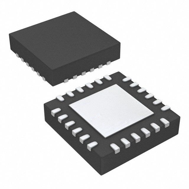
| 产品图片 |
|
| rohs | 符合RoHS无铅 / 符合限制有害物质指令(RoHS)规范要求 |
| 产品系列 | 电源管理 IC,电池管理,Texas Instruments BQ24161BRGET- |
| 数据手册 | |
| 产品型号 | BQ24161BRGET |
| 产品种类 | 电池管理 |
| 产品类型 | Charge Management |
| 供应商器件封装 | 24-VQFN (4x4) |
| 其它名称 | 296-34983-2 |
| 功能 | 充电管理,电源管理 |
| 包装 | 带卷 (TR) |
| 商标 | Texas Instruments |
| 安装类型 | 表面贴装 |
| 安装风格 | SMD/SMT |
| 封装 | Reel |
| 封装/外壳 | 24-VFQFN 裸露焊盘 |
| 封装/箱体 | VQFN-24 |
| 工作温度 | -40°C ~ 85°C |
| 工作电源电压 | 4 V to 10 V |
| 工作电源电流 | 15 mA |
| 工厂包装数量 | 250 |
| 最大工作温度 | + 85 C |
| 最小工作温度 | - 40 C |
| 标准包装 | 250 |
| 温度监测 | Temperature Monitoring |
| 电压-电源 | 4.2 V ~ 10 V |
| 电池化学 | 锂离子,锂聚合物 |
| 电池类型 | Li-Ion, Li-Polymer |
| 电荷安全定时器 | Charge Safety Timers |
| 系列 | BQ24161B |
| 输出电压 | Adjustable |
| 输出电流 | 2.5 A |


- 商务部:美国ITC正式对集成电路等产品启动337调查
- 曝三星4nm工艺存在良率问题 高通将骁龙8 Gen1或转产台积电
- 太阳诱电将投资9.5亿元在常州建新厂生产MLCC 预计2023年完工
- 英特尔发布欧洲新工厂建设计划 深化IDM 2.0 战略
- 台积电先进制程称霸业界 有大客户加持明年业绩稳了
- 达到5530亿美元!SIA预计今年全球半导体销售额将创下新高
- 英特尔拟将自动驾驶子公司Mobileye上市 估值或超500亿美元
- 三星加码芯片和SET,合并消费电子和移动部门,撤换高东真等 CEO
- 三星电子宣布重大人事变动 还合并消费电子和移动部门
- 海关总署:前11个月进口集成电路产品价值2.52万亿元 增长14.8%


.jpg)
PDF Datasheet 数据手册内容提取
Product Order Technical Tools & Support & Folder Now Documents Software Community bq24160,bq24160A,bq24161 bq24161B,bq24163,bq24168 SLUSAO0G–NOVEMBER2011–REVISEDDECEMBER2015 bq2416xx 2.5A, Dual-Input, Single-Cell Switched-Mode Li-Ion Battery Charger with Power 2 Path Management and I C Interface 1 Features 2 Applications • High-EfficiencySwitched-ModeChargerwith • HandheldProducts 1 SeparatePowerPathControl • PortableMediaPlayers – InstantlyStartUpSystemfromaDeeply • PortableEquipment DischargedBatteryorNoBattery • NetbookandPortableInternetDevices • CompatiblewithMaxLife™TechnologyforFaster ChargingWhenUsedinConjunctionWith 3 Description bq27530 The bq24160, bq24160A, bq24161, bq24161B, • DualInput,IntegratedFETChargerforupto2.5-A bq24163, and bq24168 are highly integrated single- Charging cell Li-Ion battery charger and system power path management devices targeted for space-limited, – 20-Vinputrating,withOvervoltageProtection portable applications with high-capacity batteries. The (OVP) single-cell charger has dual inputs which allow – 6.5VforUSBInputupto1.5A operation from either a USB port or a higher-power – 10.5VforINinput(bq24160,bq24160A, input supply (that is, AC adapter or wireless charging bq24161,bq24163)upto2.5A input) for a versatile solution. The two inputs are fully isolated from each other and are easily selectable – 6.5VforINinput(bq24168)upto2.5A usingtheI2Cinterface. • SafeandAccurateBattery-Management The power path management feature allows the Functions bq2416xx to power the system from a high-efficiency – 1%BatteryRegulationAccuracy DC-DC converter while simultaneously and – 10%ChargeCurrentAccuracy independently charging the battery. The power-path • ChargeParametersProgrammedUsingI2C management architecture enables the system to run with a defective or absent battery pack and enables Interface instant system turnon even with a totally discharged • Voltage-Based,NTCMonitoringInput batteryornobattery. – JEITACompatible(bq24160,bq24160A, bq24161B,bq24163,bq24168) DeviceInformation • Availableinsmall2.8-mm× 2.8-mm49-ball PARTNUMBER PACKAGE BODYSIZE(NOM) WCSPor4-mm×4-mmVQFN-24Packages VQFN(24) 4.00mm×4.00mm bq2416xx DSBGA(49) 2.80mm×2.80mm (1) For all available packages, see the orderable addendum at theendofthedatasheet. 4 Application Schematic ACAdapter or IN SW Wireless Power System PMIDI Load VBUS USB BOOT D+ D– SYS GND PMIDU D+ D– SDA BAT SCL HOST INT TEMP PACK+ TS PGND DRV + VSYS – PACK– 1 An IMPORTANT NOTICE at the end of this data sheet addresses availability, warranty, changes, use in safety-critical applications, intellectualpropertymattersandotherimportantdisclaimers.PRODUCTIONDATA.
bq24160,bq24160A,bq24161 bq24161B,bq24163,bq24168 SLUSAO0G–NOVEMBER2011–REVISEDDECEMBER2015 www.ti.com Table of Contents 1 Features.................................................................. 1 9.5 Programming...........................................................26 2 Applications........................................................... 1 9.6 RegisterMaps.........................................................29 3 Description............................................................. 1 10 ApplicationandImplementation........................ 34 4 ApplicationSchematic.......................................... 1 10.1 ApplicationInformation..........................................34 10.2 TypicalApplication ...............................................34 5 RevisionHistory..................................................... 2 11 PowerSupplyRecommendations..................... 38 6 DeviceComparisonTable..................................... 4 11.1 RequirementsforSYSOutput..............................38 7 PinConfigurationandFunctions......................... 4 11.2 RequirementsforCharging...................................38 8 Specifications......................................................... 6 12 Layout................................................................... 39 8.1 AbsoluteMaximumRatings......................................6 12.1 LayoutGuidelines.................................................39 8.2 HandlingRatings.......................................................6 12.2 LayoutExample....................................................40 8.3 RecommendedOperatingConditions.......................6 13 DeviceandDocumentationSupport................. 41 8.4 ThermalInformation..................................................7 13.1 RelatedLinks........................................................41 8.5 ElectricalCharacteristics...........................................7 13.2 CommunityResources..........................................41 8.6 TypicalCharacteristics............................................10 13.3 Trademarks...........................................................41 9 DetailedDescription............................................ 12 13.4 ElectrostaticDischargeCaution............................41 9.1 Overview.................................................................12 13.5 Glossary................................................................41 9.2 FunctionalBlockDiagram.......................................13 14 Mechanical,Packaging,andOrderable 9.3 FeatureDescription.................................................14 Information........................................................... 41 9.4 DeviceFunctionalModes........................................26 5 Revision History NOTE:Pagenumbersforpreviousrevisionsmaydifferfrompagenumbersinthecurrentversion. ChangesfromRevisionF(July2014)toRevisionG Page • DeletedhyperlinktounpublishedapplicationnoteSLUA727............................................................................................... 26 ChangesfromRevisionE(November2013)toRevisionF Page • AddedHandlingRatingtable,FeatureDescriptionsection,DeviceFunctionalModes,Applicationand Implementationsection,PowerSupplyRecommendationssection,Layoutsection,DeviceandDocumentation Supportsection,andMechanical,Packaging,andOrderableInformationsection................................................................ 1 • ChangedtheOrderingInformationtabletotheDeviceComparisonTable........................................................................... 4 • ChangedtoV includevaluesfor"DuringBadSourceDetection"......................................................................... 8 BAD_SOURCE • ChangedtheFunctionalBlockDiagram.ChangedthedevicenumbersaboveD+/D-andPSEL....................................... 13 • ChangedthePWMControllerinChargeModesectiontoincludethesoft-startfunction.................................................... 15 • ChangedtheBatteryChargingProcesssection.Newtextaddedstartingwith"Thebq2416xxmonitorsthecharging current.."............................................................................................................................................................................... 15 • ChangedtheInputSourceConnectedsection..................................................................................................................... 16 • ChangedtheInputSourceConnectedsection..................................................................................................................... 18 • AddedtheReverseBoost(BoostBack)PreventionCircuitsection..................................................................................... 24 ChangesfromRevisionD(November2012)toRevisionE Page • AddedFeature:CompatiblewithMaxLifeTechnologyforFasterChargingWhenUsedinConjunctionWithbq27530.......1 • ChangedFrom:QFN-24PackageTo:VQFN-24Packagethroughoutthedatasheet.......................................................... 1 2 SubmitDocumentationFeedback Copyright©2011–2015,TexasInstrumentsIncorporated ProductFolderLinks:bq24160 bq24160A bq24161bq24161B bq24163 bq24168
bq24160,bq24160A,bq24161 bq24161B,bq24163,bq24168 www.ti.com SLUSAO0G–NOVEMBER2011–REVISEDDECEMBER2015 ChangesfromRevisionC(October2012)toRevisionD Page • ChangedtheOrderingInformationtabletoincludetheWSCPpackageforbq24161BRGRandbq24161BYFF.................4 ChangesfromRevisionB(September2012)toRevisionC Page • ChangedtheOrderingInformationtabletoincludebq24160A.............................................................................................. 4 ChangesfromRevisionA(March2012)toRevisionB Page • ChangedtheOrderingInformationtabletoincludebq24161B.............................................................................................. 4 • ChangedtextFrom:"batteryFET(Q6)"To:"batteryFET(Q4)"intheBatteryOnlyConnectedsection............................ 18 • ChangedFrom:V <V <V To:V >V >V ,andChangedFrom:V <V <V To:V > WARM TS HOT WARM TS HOT COLD TS COOL COLD V >V intheExternalNTCMonitoring(TS)section.................................................................................................... 21 TS COOL • ChangedFigure33 .............................................................................................................................................................. 40 ChangesfromOriginal(November2011)toRevisionA Page • ChangedtheUSBPinnumbersintheYFFpachkageforbq24160/3From:A5-A6To:A5-A7............................................. 5 • ChangedV -Voltageregulationaccuracy ................................................................................................................... 7 BATREG • ChangedFigure21 .............................................................................................................................................................. 34 • ChangedFigure22 .............................................................................................................................................................. 35 Copyright©2011–2015,TexasInstrumentsIncorporated SubmitDocumentationFeedback 3 ProductFolderLinks:bq24160 bq24160A bq24161bq24161B bq24163 bq24168
bq24160,bq24160A,bq24161 bq24161B,bq24163,bq24168 SLUSAO0G–NOVEMBER2011–REVISEDDECEMBER2015 www.ti.com 6 Device Comparison Table TIMERS PARTNUMBER(1)(2) USBOVP INOVP USBDETECTION (WSaaftecthydaongd) MONNITTOCRING VIBBAATTSSHHRRTT/ VMINSYS 3.0V bq24160 6.5V 10.5V D+/D– Yes JEITA 3.5V 50mA 3.0V bq24160A 6.5V 10.5V D+/D– No JEITA 3.5V 50mA PSEL(0=1.5A, 2.0V bq24161 6.5V 10.5V Yes Standard 3.5V 1=100mA) 50mA PSEL(0=1.5A, 3.0V bq24161B 6.5V 10.5V Yes JEITA 3.5V 1=500mA) 50mA 2.0V bq24163 6.5V 10.5V D+/D– Yes JEITA 3.2V 50mA PSEL(0=1.5A, 2.0V bq24168 6.5V 6.5V No JEITA 3.5V 1=100mA) 50mA (1) EachoftheaboveareavailableinasYFFandRGEpackageswiththefollowingoptions: R-tabedandreeledinquantitiesof3,000devicesperreel. T-tapedandreeledinquantitiesof250devicesperreel. (2) ThisproductisRoHScompatible,includingaleadconcentrationthatdoesnotexceed0.1%oftotalproductweight,andissuitablefor useinspecifiedlead-freesolderingprocesses.Inaddition,thisproductusespackagematerialsthatdonotcontainhalogens,including bromine(Br)orantimony(Sb)above0.1%oftotalproductweight. 7 Pin Configuration and Functions RGEPackage VQFN24Pins TopView CD PMIDU USB IN PMIDI BOOT CD PMIDU USB IN PMIDI BOOT 24 23 22 21 20 19 24 23 22 21 20 19 D- 11 18SW N.C. 11 18SW D+ 22 17PGND PSEL 22 17PGND SCL 3 16SGND SCL 3 bq24161 16SGND SDA 4 bbqq2244116603 15PGND SDA 4 bbqq2244116611B8 15PGND PGND 5 14SYS GND 5 14SYS DRV 6 13SYS DRV 6 13SYS 7 8 9 10 11 12 7 8 9 10 11 12 INT STAT TS BGATE BAT BAT /BATGD STAT TS BGATE BAT BAT YFFPackage WCSP49Pins TopView bq24161 bq24160 bq24161B bq24163 bq24168 (Top View) (Top View) 1 2 3 4 5 6 7 1 2 3 4 5 6 7 A IN IN IN IN USB USB USB A IN IN IN IN USB USB USB B PMIDI PMIDI PMIDI PMIDI PMIDU PMIDU PMIDU B PMIDI PMIDI PMIDI PMIDI PMIDU PMIDU PMIDU C SW SW SW SW SW SW SW C SW SW SW SW SW SW SW D PGND PGND PGND PGND PGND PGND PGND D PGND PGND PGND PGND PGND PGND PGND E PGND D+ D- CD SDA SCL BOOT E PGND PSEL N.C. CD SDA SCL BOOT F SYS SYS SYS SYS BGATE INT DRV F SYS SYS SYS SYS BGATE INT DRV G BAT BAT BAT BAT TS STAT PGND G BAT BAT BAT BAT TS STAT PGND 4 SubmitDocumentationFeedback Copyright©2011–2015,TexasInstrumentsIncorporated ProductFolderLinks:bq24160 bq24160A bq24161bq24161B bq24163 bq24168
bq24160,bq24160A,bq24161 bq24161B,bq24163,bq24168 www.ti.com SLUSAO0G–NOVEMBER2011–REVISEDDECEMBER2015 PinFunctions PIN NO. NO. I/O DESCRIPTION NAME bq24160,3 bq24161,1B,8 YFF RGE YFF RGE BAT G1-G4 11,12 G1-G4 11,12 I/O BatteryConnection–Connecttothepositiveterminalofthebattery.Additionally,bypassBAT toGNDwithatleasta1μFcapacitor. BGATE F5 10 F5 10 O ExternalDischargeMOSFETGateConnection–BGATEdrivesanexternalP-Channel MOSFETtoprovideaverylow-resistancedischargepath.ConnectBGATEtothegateofthe externalMOSFET.BGATEislowduringhighimpedancemodeandwhennoinputisconnected. BOOT E7 19 E7 19 I HighSideMOSFETGateDriverSupply–Connecta0.01µFceramiccapacitor(voltagerating >10V)fromBOOTtoSWtosupplythegatedriveforthehighsideMOSFETs. CD E4 24 E4 24 I ICHardwareChipDisableInput–DriveCDhightoplacethebq2416xxinhigh-zmode.Drive CDlowfornormaloperation.DonotleaveCDunconnected. D+ E2 2 — — I D+andD–ConnectionsforUSBInputAdapterDetection–Whenachargecycleisinitiated bytheUSBinput,andashortisdetectedbetweenD+andD–,theUSBinputcurrentlimitisset D– E3 1 — — I to1.5A.Ifashortisnotdetected,theUSB100modeisselected.TheD+/D–detectionhasno effectontheINinput. DRV F7 6 F7 6 O GateDriveSupply–DRVisthebiassupplyforthegatedriveoftheinternalMOSFETs.Bypass DRVtoPGNDwitha1μFceramiccapacitor.DRVmaybeusedtodriveexternalloadsupto 10mA.DRVisactivewhenevertheinputisconnectedandVSUPPLY>VUVLOandVSUPPLY>(VBAT +VSLP) IN A1-A4 21 A1-A4 21 I Inputpowersupply–INisconnectedtotheexternalDCsupply(ACadapteroralternatepower source).BypassINtoPGNDwithatleasta1μFceramiccapacitor. INT F6 7 F6 7 O StatusOutput–INTisanopen-drainoutputthatsignalschargingstatusandfaultinterrupts. INTpullslowduringcharging.INTishighimpedancewhenchargingiscompleteorthecharger isdisabled.Whenafaultoccurs,a128μspulseissentoutasaninterruptforthehost.INTis enabled/disabledusingtheEN_STATbitinthecontrolregister.ConnectINTtoalogicrail througha100kΩresistortocommunicatewiththehostprocessor. PGND D1-D7, 5,15, D1-D7, 5,15, — Groundterminal–Connecttothethermalpad(forVQFNonly)andthegroundplaneofthe E1,G7 16,17 E1,G7 16,17 circuit. PMIDI B1-B4 20 B1-B4 20 O ReverseBlockingMOSFETandHighSideMOSFETConnectionPointforHighPower Input–BypassPMIDItoGNDwithatleasta4.7μFceramiccapacitor.Usecautionwhen connectinganexternalloadtoPMIDI.ThePMIDIoutputisnotcurrentlimited.Anyshorton PMIDIwilldamagetheIC. PMIDU B5-B7 23 B5-B7 23 O ReverseBlockingMOSFETandHighSideMOSFETConnectionPointforUSBInput– BypassPMIDUtoGNDwithatleasta4.7μFceramiccapacitor.Usecautionwhenconnectingan externalloadtoPMIDU.ThePMIDUoutputisnotcurrentlimited.AnyshortonPMIDUwill damagetheIC. PSEL — — E2 2 USBSourceDetectionInput–DrivePSELhightoindicatethataUSBsourceisconnectedto theUSBinput.WhenPSELishigh,theICstartsupwitha100mA(bq24161/8)or500mA (bq24161B)inputcurrentlimitforUSB.DrivePSELlowtoindicatethatanACAdapteris connectedtotheUSBinput.WhenPSELislow,theICstartsupwitha1.5Ainputcurrentlimit forUSB.PSELhasnoeffectontheINinput.DonotleavePSELunconnected. SCL E6 3 E6 3 I I2CInterfaceClock–ConnectSCLtothelogicrailthrougha10kΩresistor. SDA E5 4 E5 4 I/O I2CInterfaceData–ConnectSDAtothelogicrailthrougha10kΩresistor. STAT G6 8 G6 8 O StatusOutput–STATisanopen-drainoutputthatsignalschargingstatusandfaultinterrupts. STATpullslowduringcharging.STATishighimpedancewhenchargingiscompleteorthe chargerisdisabled.Whenafaultoccurs,a128μspulseissentoutasaninterruptforthehost. STATisenabled/disabledusingtheEN_STATbitinthecontrolregister.PullSTATuptoalogic railthruoghanLEDforvisualindicationorthrougha10kΩresistortocommunicatewiththehost processor. SW C1-C7 18 C1-C7 18 O InductorConnection–Connecttotheswitchedsideoftheexternalinductor. SYS F1-F4 13,14 F1-F4 13,14 I SystemVoltageSenseandChargerFETConnection–ConnectSYStothesystemoutputat theoutputbulkcapacitors.BypassSYSlocallywithatleast10μF.A47μFbypasscapacitoris recommendedforoptimaltransientresponse. TS G5 9 G5 9 I BatteryPackNTCMonitor–ConnectTStothecentertapofaresistordividerfromDRVto GND.TheNTCisconnectedfromTStoGND.TheTSfunctionprovides4thresholdsforJEITA compatibility(160,161B,163,168only).TSfaultsarereportedbytheI2Cinterface.Seethe NTCMonitorsectionformoredetailsonoperationandselectingtheresistorvalues.ConnectTS toDRVtodisabletheTSfunction. USB A5-A7 22 A5-A7 22 I USBInputPowerSupply–USBisconnectedtotheexternalDCsupply(ACadapterorUSB port).BypassUSBtoPGNDwithatleasta1μFceramiccapacitor. Thermal — Pad — Pad — ThereisaninternalelectricalconnectionbetweentheexposedthermalpadandthePGNDpin Pad ofthedevice.ThethermalpadmustbeconnectedtothesamepotentialasthePGNDpinonthe printedcircuitboard.Donotusethethermalpadastheprimarygroundinputforthedevice. PGNDpinmustbeconnectedtogroundatalltimes. Copyright©2011–2015,TexasInstrumentsIncorporated SubmitDocumentationFeedback 5 ProductFolderLinks:bq24160 bq24160A bq24161bq24161B bq24163 bq24168
bq24160,bq24160A,bq24161 bq24161B,bq24163,bq24168 SLUSAO0G–NOVEMBER2011–REVISEDDECEMBER2015 www.ti.com 8 Specifications 8.1 Absolute Maximum Ratings overoperatingfree-airtemperaturerange(unlessotherwisenoted)(1) MIN MAX UNIT IN,USB –2 20 V Pinvoltagerange(with PMIDI,PMIDU,BOOT –0.3 20 V respecttoVSS) SW –0.7 12 V SDA,SCL,SYS,BAT,STAT,BGATE,DRV,TS,D+,D–,INT,PSEL,CD –0.3 7 V BOOTtoSW –0.3 7 V SW 4.5 A Outputcurrent(Continuous) SYS,BAT 3.5 A IN 2.75 A Inputcurrent(Continuous) USB 1.75 A STAT 10 mA Outputsinkcurrent INT 1 mA Operatingfree-airtemperaturerange –40 85 °C Junctiontemperature,T –40 125 °C J Leadtemperature(soldering,10s) 300 °C (1) Stressesbeyondthoselistedunderabsolutemaximumratingsmaycausepermanentdamagetothedevice.Thesearestressratings only,andfunctionaloperationofthedeviceattheseoranyotherconditionsbeyondthoseindicatedunderrecommendedoperating conditionsisnotimplied.Exposuretoabsolute-maximum-ratedconditionsforextendedperiodsmayaffectdevicereliability.Allvoltage valuesarewithrespecttothenetworkgroundterminalunlessotherwisenoted. 8.2 Handling Ratings MIN MAX UNIT T Storagetemperaturerange –65 150 °C stg Humanbodymodel(HBM),perANSI/ESDA/JEDECJS-001,all 2 kV pins(1) V Electrostaticdischarge (ESD) Chargeddevicemodel(CDM),perJEDECspecification 500 V JESD22-C101,allpins(2) (1) JEDECdocumentJEP155statesthat500-VHBMallowssafemanufacturingwithastandardESDcontrolprocess. (2) JEDECdocumentJEP157statesthat250-VCDMallowssafemanufacturingwithastandardESDcontrolprocess. 8.3 Recommended Operating Conditions overoperatingfree-airtemperaturerange(unlessotherwisenoted) MIN MAX UNIT INvoltagerange 4.2 18 V INoperatingvoltagerange(bq24160/1/3) 4.2 10 V IN INoperatingvoltagerange(bq24168) 4.2 6 USBvoltagerange 4.2 18 V V USB USBoperatingrange 4.2 6 I Inputcurrent,INinput 2.5 A IN I InputcurrentUSBinput 1.5 A USB I OutputCurrentfromSW,DC 3 A SYS Charging 2.5 A I BAT Discharging,usinginternalbatteryFET 2.5 A T Operatingjunctiontemperaturerange 0 125 ºC J 6 SubmitDocumentationFeedback Copyright©2011–2015,TexasInstrumentsIncorporated ProductFolderLinks:bq24160 bq24160A bq24161bq24161B bq24163 bq24168
bq24160,bq24160A,bq24161 bq24161B,bq24163,bq24168 www.ti.com SLUSAO0G–NOVEMBER2011–REVISEDDECEMBER2015 8.4 Thermal Information bq2416xx THERMALMETRIC(1) UNIT 49PINS(YFF) 24PINS(RGE) θ Junction-to-ambientthermalresistance 49.8 32.6 °C/W JA θ Junction-to-case(top)thermalresistance 0.2 30.5 °C/W JCtop θ Junction-to-boardthermalresistance 1.1 3.3 °C/W JB ψ Junction-to-topcharacterizationparameter 1.1 0.4 °C/W JT ψ Junction-to-boardcharacterizationparameter 6.6 9.3 °C/W JB θ Junction-to-case(bottom)thermalresistance n/a 2.6 °C/W JCbot (1) Formoreinformationabouttraditionalandnewthermalmetrics,seetheICPackageThermalMetricsapplicationreport,SPRA953. 8.5 Electrical Characteristics CircuitofFigure21,V =V orV (whicheverissupplyingtheIC),V <V <V andV >V +V ,T SUPPLY USB IN UVLO SUPPLY OVP SUPPLY BAT SLP J =-40°C–125°CandT =25ºCfortypicalvalues(unlessotherwisenoted) J PARAMETER TESTCONDITIONS MIN TYP MAX UNIT INPUTCURRENTS VUVLO<VSUPPLY<VOVPand PWMswitching 15 mA ISUPPLY Supplycurrentforcontrol(VINorVUSB) VSUPPLY>VBAT+VSLP PWMNOTswitching 5 0°C<TJ<85°C,High-ZMode 175 μA IBATLEAK LeakagecurrentfromBATtotheSupply 0°C<TJ<85°C,VBAT=4.2V,VUSB=VIN=0V 5 μA IBAT_HIZ B(BaAttTe,rySdWis,cShYarSg)ecurrentinHighImpedancemode, 0S°CCL<,STJD<A8=50°CV,VorBA1T.8=V4,.H2Vig,hV-ZSUMPPoLdYe=5Vor0V, 55 μA POWER-PATHMANAGEMENT bq24160,1,1B,8 3.60 3.7 3.82 ChargeEnabled,VBAT<VMINSYS bq24163 3.3 3.4 3.5 VSYS(REG) Systemregulationvoltage V BatteryFETturnedoff(ChargeDisabled,TSFaultor VBATREG VBATREG VBATREG ChargingTerminated) +1.5% +3.0% +4.17% VMINSYS Minimumsystemregulationvoltage CInhpaurtgceurerneanbtlleimd,itVoBrAVTI<NDVPMMINaScYtSiv,e bbqq2244116603,1,1B,8 33..41 33..52 33.6.32 VV VBSUP1 Entersupplementmodethreshold VBAT>2.5V –30VmBAVT V VBSUP2 Exitsupplementmodethreshold VBAT>2.5V –10VmBAVT V ILIM(discharge) Currentlimit,dischargeorsupplementmode CurrentmonitoredininternalFETonly. 7 A tDGL(SC1) Dsuepgpliltecmhetinmtem,oSdYeSshortcircuitduringdischargeor Mimepaesduarnecdefrom(VBAT–VSYS)=300mVtoBAThigh- 250 μs Recoverytime,SYSshortcircuitduringdischargeor tREC(SC1) supplementmode 60 ms BatteryrangeforBGATEandsupplementmode 2.5 4.5 V operation BATTERYCHARGER MeasuredfromBATtoSYS, YFFpkg 37 57 RON(BAT-SYS) InternalbatterychargerMOSFETon-resistance VBAT=4.2V RGEpkg 50 70 mΩ ChargeVoltage Operatinginvoltageregulation,Programmablerange 3.5 4.44 V VBATREG Voltageregulationaccuracy –1% 1% ICHARGE FFaassttcchhaarrggeeccuurrrreennttraacncgueracy V0°BCATStoHR1T2≤5°VCBAT<VBAT(REG)programmablerange –1505%0 +21500%0 mA bq24161,3,8 1.9 2.0 2.1 VBATSHRT Batteryshortcircuitthreshold 100mVHysteresis bq24160,1B 2.9 3.0 3.1 V IBATSHRT Batteryshortcircuitcurrent VBAT<VBATSHRT 50 mA Deglitchtimeforbatteryshortcircuittofastcharge tDGL(BATSHRT) transition 32 ms ITERM Terminationchargecurrentaccuracy IITTEERRMM=≥15000mmAA ––3155%% ++3155%% tDGL(TERM) Deglitchtimeforchargetermination Bothrisingandfalling,2mVoverdrive,tRISE,tFALL=100ns 32 ms VRCH Rechargethresholdvoltage BelowVBATREG 120 mV tDGL(RCH) Deglitchtime VBATfallingbelowVRCH,tFALL=100ns 32 ms Copyright©2011–2015,TexasInstrumentsIncorporated SubmitDocumentationFeedback 7 ProductFolderLinks:bq24160 bq24160A bq24161bq24161B bq24163 bq24168
bq24160,bq24160A,bq24161 bq24161B,bq24163,bq24168 SLUSAO0G–NOVEMBER2011–REVISEDDECEMBER2015 www.ti.com Electrical Characteristics (continued) CircuitofFigure21,V =V orV (whicheverissupplyingtheIC),V <V <V andV >V +V ,T SUPPLY USB IN UVLO SUPPLY OVP SUPPLY BAT SLP J =-40°C–125°CandT =25ºCfortypicalvalues(unlessotherwisenoted) J PARAMETER TESTCONDITIONS MIN TYP MAX UNIT VDETECT Batterydetectionthreshold Duringbatterydetectionsourcecycle 3.3 V Duringbatterydetectionsinkcycle 3.0 IDETECT Batterydetectioncurrentbeforechargedone(sink Terminationenabled(EN_TERM=1) 2.5 mA current) tDETECT Batterydetectiontime Terminationenabled(EN_TERM=1) 250 ms VIH PSEL,CDInputhighlogiclevel 1.3 V VIL PSEL,CDInputlowlogiclevel 0.4 V INPUTCURRENTLIMITING IUSBLIM=USB100 90 95 100 IUSBLIM=USB500 450 475 500 IIN_USB Inputcurrentlimitthreshold(USBinput) UDSCBCcuhrraerngtepmuloledde,frVoUmSBS=W5V, IIUUSSBBLLIIMM==UUSSBB910500 183050 14825.50 195000 mA IUSBLIM=USB800 700 750 800 IUSBLIM=1.5A 1250 1400 1500 IIN_IN Inputcurrentlimitthreshold(INinput) IDNCcChaurrgreenmtpoudlele,dVfINro=m5SVW, IIIINNLLIIMM==12..55AA 12.3.35 12..55 12.6.85 A VIN_DPM InputbasedDPMthresholdrange Chargemode,programmableviaI2C,bothinputs 4.2 4.76 V VIN_DPMthresholdaccuracy –2 +2% VDRVBIASREGULATOR VDRV Internalbiasregulatorvoltage VSUPPLY>5.45V 5 5.2 5.45 V IDRV DRVoutputcurrent 10 mA VDO_DRV DRVDropoutvoltage(VSUPPLY–VDRV) ISUPPLY=1A,VSUPPLY=5V,IDRV=10mA 450 mV STATUSOUTPUT(STAT,INT) VOL Low-leveloutputsaturationvoltage IO=10mA,sinkcurrent 0.4 V IIH High-levelleakagecurrent VSTAT=VINT=5V 1 µA PROTECTION VUVLO ICactivethresholdvoltage VINrising 3.6 3.8 4 V VUVLO_HYS ICactivehysteresis VINfallingfromaboveVUVLO 120 150 mV VSLP Sleep-modeentrythreshold,VSUPPLY-VBAT 2.0V≤VBAT≤VBATREG,VINfalling 0 40 100 mV VSLP_EXIT Sleep-modeexithysteresis 2.0V≤VBAT≤VBATREG 40 100 175 mV DeglitchtimeforsupplyrisingaboveVSLP+VSLP_EXIT Risingvoltage,2mVoverdrive,tRISE=100ns 30 ms AfterBadSourceDetectioncompletes VIN_DPM V –80mV VBAD_SOURCE Badsourcedetectionthreshold DuringBadSourceDetection VIN_DPM V +80mV tDGL(BSD) Deglitchonbadsourcedetection 32 ms USB,VUSBRising 6.3 6.5 6.7 VOVP InputsupplyOVPthresholdvoltage IN,VINRising(bq24160/1/1B/3) 10.3 10.5 10.7 V IN,VINRising(bq24168) 6.3 6.5 6.7 VOVP(HYS) VOVPhysteresis SupplyfallingfromVOVP 100 mV 1.025× 1.05× 1.075× VBOVP BatteryOVPthresholdvoltage VBATthresholdoverVOREGtoturnoffchargerduringcharge VBATREG VBATREG VBATREG V %of VBOVPhysteresis LowerlimitforVBATfallingfromaboveVBOVP 1 VBATREG tDGL(BOVP) BatteryOVPdeglitch BOVPfaultshowninregisteroncetDGL(BOVP)expires. 1 ms BuckconvertershutdownimmediatelywhenVBAT>VBATOVP VBATUVLO Batteryundervoltagelockoutthreshold VBATrising,100mVhysteresis 2.5 V ILIMIT Cycle-by-cyclecurrentlimit VSYSshorted 4.1 4.9 5.6 A TSHTDWN Thermaltrip 165 °C Thermalhysteresis 10 TREG Thermalregulationthreshold Chargecurrentbeginstocutoff 120 °C Safetytimeraccuracy (bq24160/1/1B/3Only) –20% 20% PWM InternaltopreverseblockingMOSFETon-resistance IIN_LIMIT=500mA,MeasuredfromUSBtoPMIDU 95 175 mΩ IIN_LIMIT=500mA,MeasuredfromINtoPMIDI 45 80 8 SubmitDocumentationFeedback Copyright©2011–2015,TexasInstrumentsIncorporated ProductFolderLinks:bq24160 bq24160A bq24161bq24161B bq24163 bq24168
bq24160,bq24160A,bq24161 bq24161B,bq24163,bq24168 www.ti.com SLUSAO0G–NOVEMBER2011–REVISEDDECEMBER2015 Electrical Characteristics (continued) CircuitofFigure21,V =V orV (whicheverissupplyingtheIC),V <V <V andV >V +V ,T SUPPLY USB IN UVLO SUPPLY OVP SUPPLY BAT SLP J =-40°C–125°CandT =25ºCfortypicalvalues(unlessotherwisenoted) J PARAMETER TESTCONDITIONS MIN TYP MAX UNIT InternaltopN-channelSwitchingMOSFETon- MeasuredfromPMIDUtoSW 100 175 mΩ resistance MeasuredfromPMIDItoSW 65 110 InternalbottomN-channelMOSFETon-resistance MeasuredfromSWtoPGND 65 115 mΩ fOSC Oscillatorfrequency 1.35 1.50 1.65 MHz DMAX Maximumdutycycle 95% DMIN Minimumdutycycle 0% BATTERY-PACKNTCMONITOR VVHHOYST(HOT) HHiygshtetreemsipseorantuhrigehththrereshshooldld VVTTSSfraislliinngg 29.7 310 30.5 %VDRV VVWHYASR(MWARM) HHiygshtetreemsipseorantuhrigehththrereshshooldld VVTTSSfraislliinngg 37.9 38.13 39.6 %VDRV VVCHOYSO(LCOOL) LHoywsteteremspiseroantulorewththreresshhooldld VVTTSSfraislliinngg 56 56.15 56.9 %VDRV VVCHOYSL(DCOLD) LHoywsteteremspiseroantulorewththreresshhooldld VVTTSSfraislliinngg 59.5 610 60.4 %VDRV TSOFF TSDisablethreshold VTSrising,2%VDRVhysteresis 70 73 %VDRV tDGL(TS) DeglitchtimeonTSchange 50 ms D+/D–DETECTION(bq24160) VD+_SRC D+VoltageSource 0.5 0.6 0.7 V ID+_SRC D+ConnectionCheckCurrentSource 7 14 µA ID-_SINK D-CurrentSink 50 100 150 µA ID_LKG LeakageCurrentintoD+/D- D–,switchopen –1 1 µA D+,switchopen –1 1 µA VD+_LOW D+LowComparatorThreshold 0.8 V VD-_LOWdatref D-LowComparatorThreshold 250 400 mV RD-_DWN D-PulldownforConnectionCheck 14.25 24.8 kΩ BATGDOPERATION VBATGD GoodBatterythreshold 3.6 3.8 3.9 V Deglitchforgoodbatterythreshold VBATrisingtoHIGH-Zmode,DEFAULTModeOnly 32 ms I2CCOMPATIBLEINTERFACE VIH Inputlowthresholdlevel VPULL-UP=1.8V,SDAandSCL 1.3 V VIL Inputlowthresholdlevel VPULL-UP=1.8V,SDAandSCL 0.4 V VOL Outputlowthresholdlevel IL=10mA,sinkcurrent 0.4 V IBIAS High-Levelleakagecurrent VPULL-UP=1.8V,SDAandSCL 1 μA tWATCHDOG Watchdogtimertimeout (bq24160/1/3Only) 30 s Copyright©2011–2015,TexasInstrumentsIncorporated SubmitDocumentationFeedback 9 ProductFolderLinks:bq24160 bq24160A bq24161bq24161B bq24163 bq24168
bq24160,bq24160A,bq24161 bq24161B,bq24163,bq24168 SLUSAO0G–NOVEMBER2011–REVISEDDECEMBER2015 www.ti.com 8.6 Typical Characteristics 100 100 90 90 80 80 70 70 %) %) y ( 60 y ( 60 nc 50 nc 50 e e Effici 40 Effici 40 30 30 20 VIN = 5 V 20 10 VIN = 7 V 10 VUSB = 5 V VIN = 9 V VUSB = 6 V 0 0 0.1 1 3 0.1 1 2 System Current (A) System Current (A) G001 G002 ChargeDisabled ChargeDisabled SYSloaded SYSloaded V =3.6V V =3.6V BATREG BATREG IN2500ILIM USB1500ILIM Figure1.INEfficiency Figure2.USBEfficiency 3.9 4.21 V) SYSREG Regulation n ( 3.85 MINSYS Regulation 4.208 o egulati 3.37.58 n (V) 44..220046 R o S 3.7 ati 4.202 Y ul S 3.65 g 4.2 N e G and MI 3.35.56 Battery R 44..119968 E 3.5 4.194 R YS 3.45 4.192 S 3.4 4.19 −50 0 50 100 150 0 25 50 75 100 125 Temperature (°C) Temperature (°C) G003 G004 V =3V V =4.2V BAT BATREG Noload TerminationDisabled Figure3.SYSREGandMINSYSRegulationvsTemperature Figure4.BatteryRegulationvsTemperature 700 6.7 USB100 Current Limit Falling Edge A) 600 USB500 Current Limit 6.6 Rising Edge m V) Limit ( 500 hold ( 6.5 Current 340000 P Thres 66..34 ut OV np 200 V 6.2 SB I 6.5 U 100 6.1 0 6 −50 0 50 100 150 −50 0 50 100 150 Temperature (°C) Temperature (°C) G005 G006 USB100andUSB500currentlimit USBinputandINinput(bq24168) V =5V USB V =3.6V BAT Figure5.USBInputCurrentLimitvs.Temperature Figure6.6.5VOVPThresholdvs.Temperature 10 SubmitDocumentationFeedback Copyright©2011–2015,TexasInstrumentsIncorporated ProductFolderLinks:bq24160 bq24160A bq24161bq24161B bq24163 bq24168
bq24160,bq24160A,bq24161 bq24161B,bq24163,bq24168 www.ti.com SLUSAO0G–NOVEMBER2011–REVISEDDECEMBER2015 Typical Characteristics (continued) 10.7 2.1 Falling Edge 2.09 10.6 Rising Edge V) 2.08 eshold ( 1100..45 ent (A) 22..0067 5 V OVP Thr 1100..23 Charge Curr 222...000345 10. 2.02 10.1 2.01 10 2 −50 0 50 100 150 2 2.5 3 3.5 4 4.5 Temperature (°C) Battery Voltage (V) G007 G008 I =2A CHARGE V =5V IN V =4.44V BATREG Figure7.10.5VOVPThresholdvs.Temperature Figure8.ChargeCurrentvs.BatteryVoltage 0.055 0.054 A) 0.053 (RT H S AT0.052 B I 0.051 0.05 0 0.5 1 1.5 2 2.5 3 Battery Voltage (V) G009 Figure9.I vs.BatteryVoltage BATSHRT Copyright©2011–2015,TexasInstrumentsIncorporated SubmitDocumentationFeedback 11 ProductFolderLinks:bq24160 bq24160A bq24161bq24161B bq24163 bq24168
bq24160,bq24160A,bq24161 bq24161B,bq24163,bq24168 SLUSAO0G–NOVEMBER2011–REVISEDDECEMBER2015 www.ti.com 9 Detailed Description 9.1 Overview The bq24160/bq24160A/bq24161/bq24161B/bq24163/bq24168 devices are highly integrated single-cell Li-Ion battery chargers and system power path management devices targeted for space-limited, portable applications with high-capacity batteries. The dual-input, single-cell charger operates from either a USB port or alternate powersource(thatis,walladapterorwirelesspowerinput)foraversatilesolution. The power path management feature allows the bq2416xx to power the system from a high-efficiency DC-DC converter while simultaneously and independently charging the battery. The charger monitors the battery current at all times and reduces the charge current when the system load requires current above the input current limit. This allows proper charge termination and enables the system to run with a defective or absent battery pack. Additionally, this enables instant system turnon even with a totally discharged battery or no battery. The power- path management architecture also permits the battery to supplement the system current requirements when the adapter cannot deliver the peak system currents. This enables the use of a smaller adapter. The 2.5-A current capability allows for GSM phone calls as soon as the adapter is plugged in regardless of the battery voltage. The chargeparametersareprogrammableusingtheI2Cinterface. 12 SubmitDocumentationFeedback Copyright©2011–2015,TexasInstrumentsIncorporated ProductFolderLinks:bq24160 bq24160A bq24161bq24161B bq24163 bq24168
bq24160,bq24160A,bq24161 bq24161B,bq24163,bq24168 www.ti.com SLUSAO0G–NOVEMBER2011–REVISEDDECEMBER2015 9.2 Functional Block Diagram PMIDU PMIDI 5.2-VReference DRV IN Q1 USB 5A + BOOT CbC Current Limit IN IINLIM USB IUSBLIM IN VINDPM DC-DC CONVERTER Q2 USB VINDPM COPMWPMENLOSGATICIO,N VSYS(REG) BATTERYFAENTDCONTROL IBAT(REG) VBAT(REG) SW DIETemp Regulation Q3 PGND VSUPPLY References SYS SUPPLY_SEL VUSB + Termination VUSBOVP Reference OVPComparators + IBAT Q4 TerminationComparator VIN + VINOVP Recharge Comparator BAT Start Recharge + VBATREG–0.12V VUSB + Cycle VBAT VBAT+VSLP VSYSREGComparator SleepComparators Enable Linear + VSYS VIN + Charge VMINSYS VBAT+VSLP GoodBattery + VBAT Hi-ZMode BGATE Circuit VBATGD CD Hi-ZMode VBATSCComparator Enable + VBAT SDA IBATSHRT VBATSHRT I2C Supplement Comparator SCL Interface + + VSYS bq24160, 60A, 3 VBAT VBSUP VDRV VBOVPComparator D+ DAedUteaScpBttieorn 1.5A/USB100 + VVBBAATTOVP D– Circuitry + DISABLE TS COLD bq24161, 1B, 8 bq24160/2/3 + 1C/0.5C PSEL TS COOL + STAT VBATREG–0.14V TS WARM + DISABLE TS HOT INT CHARGE TS CONTROLLER withTimers (160/1/3) Copyright©2011–2015,TexasInstrumentsIncorporated SubmitDocumentationFeedback 13 ProductFolderLinks:bq24160 bq24160A bq24161bq24161B bq24163 bq24168
bq24160,bq24160A,bq24161 bq24161B,bq24163,bq24168 SLUSAO0G–NOVEMBER2011–REVISEDDECEMBER2015 www.ti.com 9.3 Feature Description 9.3.1 ChargeModeOperation 9.3.1.1 ChargeProfile The internal battery MOSFET is used to charge the battery. When the battery is above the MINSYS voltage, the internal FET is on to maximize efficiency and the PWM converter regulates the charge current into the battery. When battery is less than MINSYS, the SYS is regulated to V and battery is charged using the battery SYS(REG) FETtoregulatethechargecurrent.Thereare5loopsthatinfluencethechargecurrent: • Constantcurrentloop(CC) • Constantvoltageloop(CV) • Thermal-regulationloop • Minimumsystem-voltageloop(MINSYS) • Input-voltagedynamicpower-managementloop(V -DPM) IN Duringthechargingprocess,allfiveloopsareenabledandtheonethatisdominanttakescontrol.Thebq2416xx supports a precision Li-Ion or Li-Polymer charging system for single-cell applications. The Dynamic Power Path Management (DPPM) feature regulates the system voltage to a minimum of V , so that startup is enabled MINSYS even for a missing or deeply discharged battery. Figure 10 shows a typical charge profile including the minimum systemoutputvoltagefeature. Precharge Current Regulation Voltage Regulation Phase Phase Phase Regulation voltage Charge Current Regulation Threshold System Voltage VSYS VBATSHORT Battery Voltage Charge Current Termination Current Threshold IBATSHORT Linear Charge to Maintain Battery 50mAPrecharge to Minimum Battery FET is ON FET Close Pack Protector System is OFF Voltage Figure10. Typicalbq2416xxChargingProfile 14 SubmitDocumentationFeedback Copyright©2011–2015,TexasInstrumentsIncorporated ProductFolderLinks:bq24160 bq24160A bq24161bq24161B bq24163 bq24168
bq24160,bq24160A,bq24161 bq24161B,bq24163,bq24168 www.ti.com SLUSAO0G–NOVEMBER2011–REVISEDDECEMBER2015 Feature Description (continued) 9.3.1.2 PWMControllerinChargeMode The bq2416xx provides an integrated, fixed-frequency 1.5MHz voltage-mode controller to power the system and supply the charge current. The voltage loop is internally compensated and provides enough phase margin for stable operation, allowing the use of small ceramic capacitors with low ESR. When starting up, the bq2416xx uses a "soft-start" function to help limit inrush current. When coming out of High Impedance mode, the bq2416xx starts up with the input current limit set to 40% of the value programmed in the I2C register. After 80ms, the input current limit threshold steps up in 256µs steps. The steps are 40% to 50%, then 50% to 60%, then 60% to 70%, then 70% to 80%, and finally 80% to 100%. After the final step, soft start is complete and will not be restarted untilthebq2416xxentersHighImpedancemode. The input scheme for the bq2416xx prevents battery discharge when the supply voltages are lower than VBAT and also isolates the two inputs from each other. The high-side N-MOSFET (Q1/Q2) switches to control the power delivered to the output. The DRV LDO provides a supply for the gate drive for the low side MOSFET, while a bootstrap circuit (BST) with an external bootstrap capacitor is used to boost up the gate drive voltage for Q1andQ2. Both inputs are protected by a cycle-by-cycle current limit that is sensed through the high-side MOSFETs for Q1 and Q2. The threshold for the current limit is set to a nominal 5A peak current. The inputs also utilize an input currentlimitthatlimitsthecurrentfromthepowersource. 9.3.2 BatteryChargingProcess Assuming a vaild input source is attached to IN or USB, as soon as a deeply discharged or shorted battery is attached to the BAT pin, (V < V ), the bq2416xx applies I to close the pack protector switch and BAT BATSHRT BATSHRT bring the battery voltage up to acceptable charging levels. During this time, the battery FET is linearly regulated and the system output is regulated to V . Once the battery rises above V , the charge current is SYS(REG) BATSHRT regulated to the value set in the I2C register. The battery FET is linearly regulated to maintain the system voltage at V . Under normal conditions, the time spent in this region is a very short percentage of the total SYS(REG) charging time, so the linear regulation of the charge current does not affect the overall charging efficiency for very long. If the die temperature does rise, the thermal regulation circuit reduces the charge current to maintain a die temperature less than 120°C. If the current limit for the SYS output is reached (limited by the input current limit, or V ), the SYS output drops to the V output voltage. When this happens, the charge current is IN_DPM MINSYS reduced to provide the system with all the current that is needed while maintaining the minimum system voltage. If the charge current is reduced to 0mA, pulling further current from SYS causes the output to fall to the battery voltageandentersupplementmode.(SeetheDynamicPowerPathManagement sectionformoredetails.) OncethebatteryischargedenoughsothatthesystemvoltagebeginstoriseaboveV ,thebatteryFETis SYS(REG) turned on fully and the battery is charged with the full programmed charge current set by the I2C interface, I . The slew rate for the fast-charge current is controlled to minimize current and voltage overshoot during CHARGE transients. The charge current is regulated to I until the battery is charged to the regulation voltage. As the CHARGE battery voltage rises above VRCH, the battery regulation loop is activated. This may result in a small step down in the charge current as the loops transition between the charge current and charge voltage loops. As the battery voltage charges up to the regulation voltage, V , the charge current is tapered down as shown in Figure 10 BATREG while the SYS output remains connected to the battery. The voltage between the BAT and PGND pins is regulatedtoV .Thebq2416xxisafixedsingle-cellvoltageversion,withadjustableregulationvoltage(3.5V BATREG to4.44V),programmedusingtheI2Cinterface. The bq2416xx monitors the charging current during the voltage-regulation phase. If the battery voltage is above the recharge threshold and the charge current has naturally tapered down to and remains below termination threshold, I , (without disturbance from events like supplement mode) for 32ms, the charger terminates TERM charge, turns off the battery charging FET and enters battery detection. Termination is disabled when the charge current is reduced by a loop other than the voltage regulation loop or the input current limit is set to 100 mA. For example, when the bq2416xx is in half charge due to TS function, reverse boost protection is active, LOW_CHG bit is set, or the thermal regulation, V or input current loops are active, termination will not occur. This INDPM prevents false termination events. During termination, the system output is regulated to the V and SYS(REG) supportsthefullcurrentavailablefromtheinputandthebatterysupplementmodeisavailable.(SeetheDynamic Copyright©2011–2015,TexasInstrumentsIncorporated SubmitDocumentationFeedback 15 ProductFolderLinks:bq24160 bq24160A bq24161bq24161B bq24163 bq24168
bq24160,bq24160A,bq24161 bq24161B,bq24163,bq24168 SLUSAO0G–NOVEMBER2011–REVISEDDECEMBER2015 www.ti.com Feature Description (continued) Power Path Management section for more details.) The termination current level is programmable. When setting the termination threshold less than 150mA, the reverse boost protection may trip falsely with load transients and very fully charged batteries. This will prevent termination while in the reverse boost protection and may extend charge time. To disable the charge current termination, the host sets the charge termination bit (TE) of charge controlregisterto0,refertoI2Csectionfordetails. AnewchargecycleisinitiatedifCDislowwheneither 1. V risesaboveUVLOwhileabatterywithV <V -V isattachedor SUPPLY BAT BATREG RCH 2. abatterywithV <V -V isattachedwhileV isaboveUVLO. BAT BATREG RCH SUPPLY WithV aboveUVLOandV(BAT) <V ,arechargecycleisinitiatedwhenoneofthefollowingconditions SUPPLY BOVP isdetected: 1. ThebatteryvoltagefallsbelowtheV -V threshold. BAT(REG) RCH 2. CEbittoggleorRESETbittoggle 3. Supplementmodeeventoccurs 4. CDpinorHI-Zbittoggle V should never be programmed less than V . If the battery is ever 5% above the regulation threshold, BAT(REG) BAT the battery OVP circuit shuts the PWM converter off immediately and the battery FET is turned on to discharge thebatterytosafeoperatinglevels.IfthebatteryOVPconditionexistsforthe1msdeglitch,abatteryOVPfaultis reported in the I2C status registers. The battery OVP fault is cleared when the battery voltage discharges below V or if the IC enters hi-impedance mode (HZ_MODE=1 or CD=1). Always write bq2416xx to high impedance RCH modebeforechangingV toclearBOVPconditiontoensureproperoperation. BATREG If the battery voltage is ever greater than VBATREG (for example, when an almost fully charged battery enters theJEITAWARMstateduetotheTSpin)butlessthanV ,thereverseboostprotectioncircuitrymayactivate BOVP as explained later in this datasheet. If the battery is ever above V , the buck converter turns off and the BOVP internal battery FET is turned on. This prevents further overcharging of the battery and allows the battery to discharge to safe operating levels. The battery OVP event does not clear until the battery voltage falls below V . RCH 9.3.3 BatteryDetection When termination conditions are met, a battery detection cycle is started. During battery detection, I is DETECT pulled from V for t to verify there is a battery. If the battery voltage remains above V for the full BAT DETECT DETECT duration of t , a battery is determined to present and the IC enters “Charge Done”. If V falls below DETECT BAT V , a “Battery Not Present” fault is signaled and battery detection continues. The next cycle of battery DETECT detection, the bq2416xx turns on I for t . If V rises to V , the current source is turned BATSHORT DETECT BAT DETECT offand after t , the battery detection continues through another current sink cycle. Battery detection DETECT continues until charge is disabled or a battery is detected. Once a battery is detected, the fault status clears and anewchargecyclebegins.Batterydetectionisnotrunwhenterminationisdisabled. 9.3.4 DynamicPowerPathManagement(DPPM) The bq2416xx features a SYS output that powers the external system load connected to the battery. This output isactivewheneverasourceisconnectedtoIN,USBorBAT.ThefollowingsectionsdiscussthebehaviorofSYS withasourceconnectedtothesupplyorabatterysourceonly. 9.3.5 InputSourceConnected When a valid input source is connected to IN or USB and the bq2416xx is NOT in High Impedance mode, the buck converter enters soft-start and turns on to power the load on SYS. The STAT/INT pin outputs a 128µs interrupt pulse to alert the host that an input has been connected. The FAULT bits indicate a normal condition, and the Supply Status register indicates that a new supply is connected. The CE bit (bit 1) in the control register (0x02) indicates whether a charge cycle is initiated. By default, the bq2416xx (CE=0) enables a charge cycle when a valid input source is connected. When the CE bit is '1' and a valid input source is connected, the battery FET is turned off and the SYS output is regulated to the V programmed by the V threshold in the SYS(REG) BATREG I2Cregister.AchargecycleisinitiatedwhentheCEbitiswrittentoa0value(cleared). 16 SubmitDocumentationFeedback Copyright©2011–2015,TexasInstrumentsIncorporated ProductFolderLinks:bq24160 bq24160A bq24161bq24161B bq24163 bq24168
bq24160,bq24160A,bq24161 bq24161B,bq24163,bq24168 www.ti.com SLUSAO0G–NOVEMBER2011–REVISEDDECEMBER2015 Feature Description (continued) When the CE bit is a 0 and a valid source is connected to IN or USB, the buck converter starts up using soft- start. A charge cycle is initiated 64ms after the buck converter iniates startup. When V is high enough that BAT V > V , the battery FET is turned on and the SYS output is connected to BAT. If the SYS voltage falls SYS SYS(REG) to V , it is regulated to that point to maintain the system output even with a deeply discharged or absent SYS(REG) battery. In this mode, the SYS output voltage is regulated by the buck converter and the battery FET linearly regulates the charge current into the battery. The current from the supply is shared between charging the battery and powering the system load at SYS. The dynamic power-path management (DPPM) circuitry of the bq2416xx monitors the current limits continuously, and if the SYS voltage falls to the V voltage, it adjusts charge MINSYS current to maintain the minimum system voltage and supply the load on SYS. If the charge current is reduced to zero and the load increases further, the bq2416xx enters battery-supplement mode. During supplement mode, thebatteryFETisturnedonandthebatterysupplementsthesystemload. When an input is connected with no battery attached and termination enabled, the startup process proceeds as normal until the termination deglitch times out. After this, the bq2416xx enters battery detection and waits for a battery to be connected. Once a battery is connected and passes battery detection, a new charge cycle begins. Once the battery is applied, the HZMODE bit or CD pin must be toggled before writing the BATREG to a higher voltage and beginning a new charge cycle. Failure to do this can result in SYS unexpectedly regulating to 15% aboveV . BATREG 2000mA 1800mA I SYS 800mA 0mA 1500mA I IN ~850mA 0mA 1A IBAT 0mA -200mA V SYS(REG) DPPM loop active V MINSYS V OUT ~3.1V Supplement Mode Figure11. ExampleDPPMResponse(V =5V,V =3.1V,1.5AInputCurrentLimit) Supply BAT Copyright©2011–2015,TexasInstrumentsIncorporated SubmitDocumentationFeedback 17 ProductFolderLinks:bq24160 bq24160A bq24161bq24161B bq24163 bq24168
bq24160,bq24160A,bq24161 bq24161B,bq24163,bq24168 SLUSAO0G–NOVEMBER2011–REVISEDDECEMBER2015 www.ti.com Feature Description (continued) 9.3.6 BatteryOnlyConnected When a battery with voltage greater than V is connected with no input source, the battery FET is turned BATUVLO onsimilartosupplementmode.Inthismode,thecurrentisnotregulated;however,thereisashortcircuitcurrent limit. If the short circuit limit is reached, the battery FET is turned off for the deglitch time (t ). After the DGL(SC1) recovery time (t ), the battery FET is turned on to test and see if the short has been removed. If it has not, REC(SC1) the FET turns off and the process repeats until the short is removed. This process is to protect the internal FET from over current. If an external FET is used for discharge, the external FET's body diode prevents the load on SYS from being disconnected from the battery. If the battery voltage is less than V , the internal battery BATUVLO FET (Q4) remains off and BAT is high-impedance. This prevents further discharging of deeply-discharged batteries. 9.3.7 BatteryDischargeFET(BGATE) Thebq2416xxcontainsaMOSFETdrivertodrivethegateofanexternaldischargeFETbetweenthebatteryand the system output. This external FET provides a low impedance path when supplying the system from the battery. Connect BGATE to the gate of the external discharge MOSFET. BGATE is on under the following conditions: 1. Noinputsupplyconnected. 2. HZ_MODEbit=1 3. CDpin=1 9.3.8 DEFAULTMode DEFAULT mode is used when I2C communication is not available. DEFAULT mode is entered in the following situations: 1. WhenthechargerisenabledandV <V beforeI2Ccommunicationisestablished BAT BATGD 2. WhenthewatchdogtimerexpireswithoutaresetfromtheI2Cinterfaceandthesafetytimerhasnotexpired. 3. When the device comes out of any fault condition (sleep mode, OVP, faulty adapter mode, etc.) before I2C communicationisestablished In DEFAULT mode, the I2C registers are reset to the default values. The 27-minute safety timer (no timer for bq24168) is reset and starts when DEFAULT mode is entered. The default value for VBATREG is 3.6V, and the default value for I is 1A. The input current limit for the IN input is set to 1.5A. The input current limit for the CHARGE USB input is determined by the D+/D– detection (bq24160/3) or PSEL (bq24161/1B/8). PSEL and D+/D– detection have no effect on the IN input. Default mode is exited by programming the I2C interface. Once I2C communication is established, PSEL has no effect on the USB input. Note that if termination is enabled and charginghasterminated,anewchargecycleisNOTinitiatedwhenenteringDEFAULTmode. 9.3.9 SafetyTimerandWatchdogTimer(bq24160/bq24161/bq24161B/bq24163only) At the beginning of charging process, the bq24160/1/1B/3 starts the safety timer. This timer is active during the entire charging process. If charging has not terminated before the safety timer expires, charging is disabled, the charge parameters are reset to the default values and the CE bit is written to a “1”. The length of the safety timer is selectable using the I2C interface. A single 128μs pulse is sent on the STAT and INT outputs and the STATx bits of the status registers are updated in the I2C. In DEFAULT mode, the safety timer can be reset and a new charge cycle initiated by input supply power on reset, removing/inserting battery or toggling the CD pin. In HOST mode, the CE bit is set to a '1' when the safety timer expires. The CE bit must be cleared to a '0' in order to resume charging and clear the safety timer fault. The safety timer duration is selectable using the TMR_X bits in the Safety Timer Register/ NTC Monitor register. Changing the safety timer duration resets the safety timer. This function prevents continuous charging of a defective battery. During the fast charge (CC) phase, several events increasethetimerdurationby2XiftheEN_2X_TMRbitissetintheregister. 1. Thesystemloadcurrentreducestheavailablechargingcurrent. 2. Theinputcurrentneededforthefastchargecurrentislimitedbytheinputcurrentloop. 3. TheinputcurrentisreducedbecausetheVINDPMloopispreventingthesupplyfromcrashing. 4. ThedevicehasenteredthermalregulationbecausetheICjunctiontemperaturehasexceededTJ(REG). 5. TheLOW_CHGbitisset. 18 SubmitDocumentationFeedback Copyright©2011–2015,TexasInstrumentsIncorporated ProductFolderLinks:bq24160 bq24160A bq24161bq24161B bq24163 bq24168
bq24160,bq24160A,bq24161 bq24161B,bq24163,bq24168 www.ti.com SLUSAO0G–NOVEMBER2011–REVISEDDECEMBER2015 Feature Description (continued) 6. ThebatteryvoltageislessthanVBATSHORT. 7. ThebatteryhasenteredtheJEITAWARMorCOLDstateviatheTSpin During these events, the timer is slowed by half to extend the timer and prevent any false timer faults. Starting a new charge cycle by VSUPPLY POR or removing/replacing the battery or resuming a charge by toggling the CE orHZ_MODEbits,resetsthesafetytimer.Additionally,thermalshutdowneventscausethesafetytimertoreset. In addition to the safety timer, the bq24160/1/1B/3 contain a watchdog timer that monitors the host through the I2C interface. Once a read/write is performed on the I2C interface, a 30-second timer (t ) is started. The WATCHDOG 30-second timer is reset by the host using the I2C interface. This is done by writing a “1” to the reset bit (TMR_RST) in the control register. The TMR_RST bit is automatically set to “0” when the 30-second timer is reset. This process continues until the battery is fully charged or the safety timer expires. If the 30-second timer expires, the IC enters DEFAULT mode where the default register values are loaded, the safety timer restarts at 27 minutes and charging continues. The I2C may be accessed again to reinitialize the desired values and restart thewatchdogtimer.ThewatchdogtimerflowchartisshowninFigure12. Start SafetyTimer Safety timer expired? Yes Safety timer fault No Charge Done? Yes USpdTaAtTe S=THAiT ChEanrtgeirn gsu ssupsepnednedded ICHG<ITERM bits mode Fault indicated in No STATregisters No I2C Read/Write performed? Yes Start30second watchdog timer Reset30second Charge Done? Yes USpdTaAtTe S=THAiT watchdog timer ICHG<ITERM bits No Yes Safety timer expired? Safety timer fault No Charging suspended Fault indicated in STATregisters No Yes No Received SW watchdog 30s timer expired? RESET? Yes Reset to default values in I2C register Restart27min safety timer Figure12. TheWatchdogTimerFlowChartforbq2416xx Copyright©2011–2015,TexasInstrumentsIncorporated SubmitDocumentationFeedback 19 ProductFolderLinks:bq24160 bq24160A bq24161bq24161B bq24163 bq24168
bq24160,bq24160A,bq24161 bq24161B,bq24163,bq24168 SLUSAO0G–NOVEMBER2011–REVISEDDECEMBER2015 www.ti.com Feature Description (continued) 9.3.10 D+,D– BasedAdapterDetectionfortheUSBInput(D+,D–,bq24160/0A/3) Thebq24160/0A/3containaD+,D– basedadapterdetectioncircuitthatisusedtoprogramtheinputcurrentlimit for the USB input during DEFAULT mode. D+, D– detection is only performed in DEFAULT mode unless forced bytheD+,D–_ENbitinhostmode.Writingtoregister2duringdetectionstopsthedetectionroutine. By default the USB input current limit is set to 100mA. When a voltage higher than UVLO is applied to the USB input, the bq24160/0A/3 performs a charger source identification to determine if it is connected to an SDP (USB port) or CDP/DCP (dedicated charger). The first step is D+, D- line connection detection as described in BC1.2. Primary detection begins 10ms after the connection detection complete. The primary detection complies with the method described in BC1.2. During primary detection, the D+, D- lines are tested to determine if the port is an SDP or CDP/DCP. If a CDP/DCP is detected the input current limit is increased to 1.5A, if an SDP is detected the current limit remains at 100mA, until changed via the I2C interface. These two steps require at least 90ms to complete but if they have not completed within 500ms, the D+, D- detection routine selects 100mA for the unknowninputsource.SecondarydetectionasdescribedinBC1.2isnotperformed. Automatic detection is performed only if V and V are less than 0.6V to avoid interfering with the USB D+ D– transceiverwhichmayalsoperformD+,D–detectionwhenthesystemisrunningnormally.However,D+,D–can beinitiatedatanytimebythehostbysettingtheD+,D– ENbitintheControl/BatteryVoltageRegisterto1.After detection is complete the D+, D– EN bit is automatically reset to 0 and the detection circuitry is disconnected fromtheD+,D– pinstoavoidinterferencewithUSBdatatransfer. WhenacommandiswrittentochangetheinputcurrentlimitintheI2C,thisoverridesthecurrentlimitselectedby D+/D– detection.D+,D– detectionhasnoeffectontheINinput. 9.3.11 USBInputCurrentLimitSelectorInput(PSEL,bq24161/161B/168only) The bq24161, bq24161B, and bq24168 contain a PSEL input that is used to program the input current limit for USB during DEFAULT mode. Drive PSEL high to indicate that a USB source is connected to the USB input and program the 100mA (bq24161/8) or 500mA (bq24161B) current limit for USB. Drive PSEL low to indicate that an AC Adapter is connected to the USB input. When PSEL is low, the IC starts up with a 1.5A current limit for USB. PSEL has no effect on the IN input. Once an I2C write is done, the PSEL has no effect on the input current limit untilthewatchdogtimerexpires. 9.3.12 HardwareChipDisableInput(CD) The bq2416xx contains a CD input that is used to disable the IC and place the bq2416xx into high-impedance mode.DriveCDlowtoenablechargeandenternormaloperation.DriveCDhightodisablechargeandplacethe bq2416xx into high-impedance mode. Driving CD high during DEFAULT mode resets the safety timer. Driving CD high during HOST mode resets the safety timer and places the bq2416xx into high impedance mode. The CDpinhasprecedenceovertheI2Ccontrol. 9.3.13 LDOOutput(DRV) The bq2416xx contains a linear regulator (DRV) that is used to supply the internal MOSFET drivers and other circuitry. Additionally, DRV supplies up to 10mA external loads to power the STAT LED or the USB transceiver circuitry. The maximum value of the DRV output is 5.45V; ideal for protecting voltage sensitive USB circuits from highvoltagefluctuationsinthesupply.TheLDOisonwheneverasupplyisconnectedtotheINorUSBinputsof thebq2416xx.TheDRVisdisabledunderthefollowingconditions: 1. V <UVLO SUPPLY 2. V <V SUPPLY SLP 3. ThermalShutdown 20 SubmitDocumentationFeedback Copyright©2011–2015,TexasInstrumentsIncorporated ProductFolderLinks:bq24160 bq24160A bq24161bq24161B bq24163 bq24168
bq24160,bq24160A,bq24161 bq24161B,bq24163,bq24168 www.ti.com SLUSAO0G–NOVEMBER2011–REVISEDDECEMBER2015 Feature Description (continued) 9.3.14 ExternalNTCMonitoring(TS) The I2C interface allows the user to easily implement the JEITA standard for systems where the battery pack thermistor is monitored by the host. Additionally, the bq2416xx provides a flexible, voltage based TS input for monitoring the battery pack NTC thermistor. The voltage at TS is monitored to determine that the battery is at a safe temperature during charging. The bq24160, bq24160A, bq24161B, bq24163, and bq24168 enable the user to easily implement the JEITA standard for charging temperature while the bq24161 only monitors the hot and coldcutofftemperaturesandleavestheJEITAcontroltothehost.TheJEITAspecificationisshownin. 1°C 0.5°C Portion of spec not covered by TS 4.25 V Implementation on bq24160 4.15 V 4.1 V T1 T2 T3 T4 T5 (0°C) (10°C) (45°C)(50°C) (60°C) Figure13. ChargeCurrentDuringTSConditions To satisfy the JEITA requirements, four temperature thresholds are monitored; the cold battery threshold (T < NTC 0°C), the cool battery threshold (0°C < T < 10°C), the warm battery threshold (45°C < T ≤ 60°C) and the NTC NTC hot battery threshold (T > 60°C). These temperatures correspond to the V , V , V , and V NTC COLD COOL WARM HOT thresholds. Charging is suspended and timers are suspended when V < V or V > V . When V > TS HOT TS COLD WARM V > V , the battery regulation voltage is reduced by 140mV from the programmed regulation threshold. TS HOT WhenV >V >V ,thechargingcurrentisreducedtohalfoftheprogrammedchargecurrent. COLD TS COOL The TS function is voltage based for maximum flexibility. Connect a resistor divider from DRV to GND with TS connectedtothecentertaptosetthethreshold.TheconnectionsareshowninFigure20.Theresistorvaluesare calculatedusingthefollowingequations: é 1 1 ù VDRV ´ RCOLD ´ RHOT ´ êV - V ú RLO= ë COLD HOTû éV ù é V ù RHOT ´ ê DRV -1ú-RCOLD ´ ê DRV -1ú V V ë HOT û ë COLD û (1) V DRV -1 V RHI= COLD 1 1 + RLO RCOLD (2) Where: V =0.60 ×V COLD DRV Copyright©2011–2015,TexasInstrumentsIncorporated SubmitDocumentationFeedback 21 ProductFolderLinks:bq24160 bq24160A bq24161bq24161B bq24163 bq24168
bq24160,bq24160A,bq24161 bq24161B,bq24163,bq24168 SLUSAO0G–NOVEMBER2011–REVISEDDECEMBER2015 www.ti.com Feature Description (continued) V =0.30 ×V HOT DRV WhereR istheNTCresistanceatthehottemperatureandR istheNTCresistanceatcoldtemperature. HOT COLD For the bq24160, bq24161B, bq24163, and bq24168, the WARM and COOL thresholds are not independently programmable. The COOL and WARM NTC resistances for a selected resistor divider are calculated using the followingequations: RLO ´ 0.564 ´ RHI RCOOL = RLO - RLO ´ 0.564 - RHI ´ 0.564 (3) RLO ´ 0.383 ´ RHI RWARM = RLO - RLO ´ 0.383 - RHI ´0.383 (4) VBAT(REG) 1 x Charge/ V DISABLE -140 mV 0.5 x Charge DRV TS COLD + TS COOL + TS WARM + V DRV TS HOT + RHI TS PACK+ TEMP bq2416x RLO PACK- Figure14. TSCircuit 9.3.15 ThermalRegulationandProtection During the charging process, to prevent chip overheating, the bq2416xx monitors the junction temperature, T , of J the die and begins to taper down the charge current once T reaches the thermal regulation threshold, T . The J REG charge current is reduced to zero when the junction temperature increases about 10°C above T . Once the REG charge current is reduced, the system current is reduced while the battery supplements the load to supply the system. This may cause a thermal shutdown of the bq2416xx if the die temperature rises too high. At any state, if T exceeds T , the bq2416xx suspends charging and disables the buck converter. During thermal J SHTDWN shutdown mode, the buck converter is turned off, all timers are suspended, and a single 128μs pulse is sent on the STAT and INT outputs and the STATx and FAULT_x bits of the status registers are updated in the I2C. A newchargingcyclebeginswhenT fallsbelowT byapproximately10°C. J SHTDWN 22 SubmitDocumentationFeedback Copyright©2011–2015,TexasInstrumentsIncorporated ProductFolderLinks:bq24160 bq24160A bq24161bq24161B bq24163 bq24168
bq24160,bq24160A,bq24161 bq24161B,bq24163,bq24168 www.ti.com SLUSAO0G–NOVEMBER2011–REVISEDDECEMBER2015 Feature Description (continued) 9.3.16 InputVoltageProtectioninChargeMode 9.3.16.1 SleepMode The bq2416xx enters the low-power sleep mode if the voltage on V falls below the sleep-mode entry SUPPLY threshold, V +V , and V is higher than the undervoltage lockout threshold, V . This feature BAT SLP SUPPLY UVLO prevents draining the battery during the absence of V . When V < V + V , the bq2416xx turns off SUPPLY SUPPLY BAT SLP the PWM converter, turns the battery FET on and drives BGATE to GND, sends a single 128μs pulse on the STAT and INT outputs and updates the STATx and FAULT_x bits in the status registers. Once V > V + SUPPLY BAT V ,theSTATxandFAULT_xbitsareclearedandthedeviceinitiatesanewchargecycle. SLP 9.3.16.2 InputVoltageBasedDPM During normal charging process, if the input power source is not able to support the programmed or default charging current, the supply voltage decreases. Once the supply drops to V (default 4.2V for both inputs), IN_DPM the input current limit is reduced to prevent further supply droop. When the IC enters this mode, the charge current is lower than the set value and the DPM_STATUS bit is set (Bit 5 in Register 05H). This feature provides IC compatibility with adapters with different current capabilities without a hardware change. Figure 15 shows the V DPM behavior to a current-limited source. In this figure the input source has a 750mA current limit and the IN– chargingissetto750mA.TheSYSloadisthenincreasedto1.2A. Adapter Voltage Falls due V IN toAdapter Current Limit 5 VAdapter rated for 750 mA Input Current Reduced by V function INDPM to PreventAdapter from Crashing I IN V SYS 750 mACharging 750 mACharging I BAT Supplement Mode 1.2ALoad Step I SYS Figure15. bq24160V DPM IN- 9.3.16.3 BadSourceDetection When a source is connected to IN or USB, the bq2416xx runs a Bad Source Detection procedure to determine if the source is strong enough to provide some current to charge the battery. A current sink is turned on (30mA for USB input, 75mA for the IN input) for 32ms. If the source is valid after the 32ms (V < V < V ), BADSOURCE SUPPLY OVP the buck converter starts up and normal operation continues. If the supply voltage falls below V during BAD_SOURCE the detection, the current sink shuts off for two seconds and then retries, a single 128μs pulse is sent on the STAT and INT outputs and the STATx and FAULT_x bits of the status registers and the battery/supply status registersareupdated.Thedetectioncircuitsretrycontinuouslyuntileitheranewsourceisconnectedtotheother input or a valid source is detected after the detection time. If during normal operation the source falls to V , the bq2416xx turns off the PWM converter, turns the battery FET on, sends a single 128μs pulse is BAD_SOURCE sent on the STAT and INT outputs and the STATx and FAULT_x bits of the status registers, and the battery/supply status registers are updated. Once a good source is detected, the STATx and FAULT_x bits are clearedandthedevicereturnstonormaloperation. Copyright©2011–2015,TexasInstrumentsIncorporated SubmitDocumentationFeedback 23 ProductFolderLinks:bq24160 bq24160A bq24161bq24161B bq24163 bq24168
bq24160,bq24160A,bq24161 bq24161B,bq24163,bq24168 SLUSAO0G–NOVEMBER2011–REVISEDDECEMBER2015 www.ti.com Feature Description (continued) If two supplies are connected, the supply with precedence is checked first. If the supply detection fails once, the deviceswitchestotheothersupplyfortwosecondsandthenretries.Thisallowstheprioritysupplytosettleifthe connection was jittery or the supply ramp was too slow to pass detection. If the priority supply fails the detection a second time, it is locked out and lower priority supply is used. Once the bad supply is locked out, it remains locked out until the supply voltage falls below UVLO. This prevents continuously switching between a weak supplyandagoodsupply. 9.3.16.4 InputOvervoltageProtection The built-in input overvoltage protection to protect the device and other downstream components against damage from overvoltage on the input supply (Voltage from V or V to PGND). During normal operation, if USB IN V >V ,thebq2416xxturnsoffthePWMconverter,turnsthebatteryFETandBGATEon,sendsasingle SUPPLY OVP 128μs pulse is sent on the STAT and INT outputs and the STATx and FAULT_x bits of the status registers and the battery/supply status registers are updated. Once the OVP fault is removed, the STATx and FAULT_x bits areclearedandthedevicereturnstonormaloperation. To allow operation with some unregulated adapters, the OVP circuit is not active during Bad Source Detection. Thisprovidessometimeforthecurrentsinktopulltheunregulatedadapterdownintoanacceptablerange.Ifthe adapter voltage is high at the end of the detection, the startup of the PWM converter does not occur. The OVP circuitisactiveduringnormaloperation,soifthesystemstandbycurrentplusthechargecurrentisnotenoughto pulldownthesource,operationissuspended. 9.3.16.5 ReverseBoost(BoostBack)PreventionCircuit A buck converter has two operating modes, continuous conduction mode (CCM) and discontinuous conduction mode (DCM). In DCM, the inductor current ramps down to zero during the switching cycle while in CCM the inductor maintains a DC level of current. Transitioning from DCM to CCM during load transients, slows down the converter's transient response for those load steps, which can result in the SYS rail drooping. To achieve the fastest possible transient reponse for this charger, this charger's synchronous buck converter is forced to run in CCM even at light loads when the buck converter would typically revert to DCM. The challenge that presents itself when forcing CCM with a charger is that the output of the buck converter now has a power source. Thus, if the battery voltage, V(BAT), is ever greater than V , the inductor current goes fully negative and pushes BATREG currentbacktotheinputsupply.Thiseffectcausestheinputsourcevoltagetoriseiftheinputsourcecannotsink current. The input over-voltage protection circuit protects the IC from damage however some input sources may bedamagedifthevoltagerises.Topreventthis,thischargerhasimplementedareverseboostpreventioncircuit. When reverse current is sensed that is not a result of the supplement comparator tripping, this circuit disables the internal battery FET and changes the feedback point to V for 1 ms. After the 1-ms timeout, the SYSREG BATFET is turned on again and the battery is tested to see if it is higher than V (negative current). The BATREG reverse current protection is only active when V > V > V - V . Having V > V > V - BOVP BAT BATREG RCH BOVP BAT BATREG V results in an approximately 100-mV, 1000-Hz ripple on SYS as seen in . The most common trigger for RCH reverse boost prevention is a load transient on SYS that requires the charger to enter battery supplement mode. When the IC enters reverse boost prevention, the IC stops charging or exits charge done which may result in the battery never reaching full charge. With termination enabled and ITERM > 150mA or with a high line impedance to the battery, the likelihood of activating the reverse boost prevention circuit is small and even when activated, the charger typically exits reverse boost prevention as the battery relaxes. With termination enabled and ITERM < 150mA or with a low impedance battery, the likelihood of activating the reverse boost prevention circuit by a load transient or even the inductor ripple current is higher. In either case, the IC resumes charging until VBAT drops below VBATREG - VRCH, resulting in the battery always charging to at least 0.97 of full charge. If full charge is required with ITERM < 150mA then the recommended solution to ensure full charge is asfollows 1. SET the charger’s enable no battery operation bit ( EN_NOBATOP) = 1 to disable the reverse boost prevention circuits. Brief, low-amplitude voltage pulses on IN may be observed as the IC enters boost back to resolve instances where VBAT is greater than the VBATREG, for example when exiting supplement mode. The I2C communication software must ensure that VBATREG is never written below VBAT. The IC automatically rewrites the VBATREG register to the default value of 3.6V when existing HOST mode. For JEITA enabled ICs, the IC automatically lowers the voltage reference to 0.98 of the VBATREG value. The softwaremustaccountfortheseinstancesaswell. 2. Disable the charger’s termination function and TS functions and use a gas gauge to control terminationandTSthroughitsindependentvoltageandcurrentmeasurements. 24 SubmitDocumentationFeedback Copyright©2011–2015,TexasInstrumentsIncorporated ProductFolderLinks:bq24160 bq24160A bq24161bq24161B bq24163 bq24168
bq24160,bq24160A,bq24161 bq24161B,bq24163,bq24168 www.ti.com SLUSAO0G–NOVEMBER2011–REVISEDDECEMBER2015 Feature Description (continued) Figure16. V(SYS)whenReverseBoostPreventionCircuitisActive 9.3.17 ChargeStatusOutputs(STAT,INT) TheSTAToutputisusedtoindicateoperationconditionsforbq2416xx. STAT is pulled low during charging when EN_STAT bit in the control register (0x02h) is set to “1”. When charge is complete or disabled, STAT is high impedance. When a fault occurs, a 128-µs pulse (interrupt) is sent out to notify the host. The status of STAT during different operation conditions is summarized in Table 1. STAT drives an LED for visual indication or can be connected to the logic rail for host communication. The EN_STAT bit in the control register (00H) is used to enable/disable the charge status for STAT. The interrupt pulses are unaffected by EN_STAT and will always be shown.TheINToutputisidenticaltoSTATandisusedtointerfacewithalowvoltagehostprocessor. Table1.STATPinSummary ChargeState STATandINTbehavior ChargeinprogressandEN_STAT=1 Low Othernormalconditions High-Impedance StatusChanges:SupplyStatusChange(pluginorremoval),safetytimerfault, 128-µspulse,thenHighImpedance watchdogexpiration,sleepmode,batterytemperaturefault(TS),batteryfault (OVPorabsent),thermalshutdown 9.3.18 GoodBatteryMonitor The bq2416xx contains a good battery monitor circuit that places the bq2416xx into high-z mode if the battery voltage is above the BATGD threshold while in DEFAULT mode. This function is used to enable compliance to thebatterychargingstandardthatpreventschargingfromanun-enumeratedUSBhostwhilethebatteryisabove the good battery threshold. If the bq2416xx is in HOST mode, it is assumed that USB host has been enumerated andthegoodbatterycircuithasnoeffectoncharging. Copyright©2011–2015,TexasInstrumentsIncorporated SubmitDocumentationFeedback 25 ProductFolderLinks:bq24160 bq24160A bq24161bq24161B bq24163 bq24168
bq24160,bq24160A,bq24161 bq24161B,bq24163,bq24168 SLUSAO0G–NOVEMBER2011–REVISEDDECEMBER2015 www.ti.com 9.4 Device Functional Modes The state machine of the bq2416x automatically changes primary states (Off, sleep, HiZ, charge disabled, charging, charge done, battery OVP, fault) based on data in the I2C registers, IN and USB pin voltages, BAT pin voltage and current flow, TS pin voltage, CD pin voltage and status of the safety timer. The BAT and TS pin voltages as well as current flow into the IN and USB pins, out of SYS pin and into/out of the BAT pin determine the charging sub-states, including conditioning, constant current (CC), CC with reduced charge current, constant voltage(CV)withreducedchargecurrent. 9.5 Programming 9.5.1 SerialInterfaceDescription The bq2416xx uses an I2C-compatible interface to program charge parameters. I2C is a 2-wire serial interface developed by Philips Semiconductor (see I2C-Bus Specification, Version 2.1, January 2000). The bus consists of a data line (SDA) and a clock line (SCL) with pull-up structures. When the bus is idle, both SDA and SCL lines are pulled high. All I2C-compatible devices connect to the I2C bus through open drain I/O pins, SDA and SCL. A master device, usually a microcontroller or a digital signal processor, controls the bus. The master is responsible for generating the SCL signal and device addresses. The master also generates specific conditions that indicate the START and STOP of data transfer. A slave device receives and/or transmits data on the bus under control of themasterdevice. Thebq2416xxdeviceworksasaslaveandsupportsthefollowingdatatransfermodes,asdefinedintheI2CBus Specification: standard mode (100kbps) and fast mode (400kbps). The interface adds flexibility to the battery charging solution, enabling most functions to be programmed to new values depending on the instantaneous application requirements. Register contents remain intact as long as battery voltage remains above 2.5V (typical). The I2C circuitry is powered from VBUS when a supply is connected. If the VBUS supply is not connected, the I2C circuitry is powered from the battery through BAT. The battery voltage must stay above 2.5V withnoinputconnectedinordertomaintainproperoperation. The data transfer protocol for standard and fast modes is exactly the same; therefore, they are referred to as the F/S-mode in this document. The bq2416xx devices only support 7-bit addressing. The device 7-bit address is definedas‘1101011’(6Bh). 9.5.1.1 F/SModeProtocol The master initiates data transfer by generating a start condition. The start condition is when a high-to-low transition occurs on the SDA line while SCL is high, as shown in Figure 17. All I2C-compatible devices should recognizeastartcondition. DATA CLK S P START Condition STOPCondition Figure17. STARTandSTOPCondition The master then generates the SCL pulses, and transmits the 8-bit address and the read/write direction bit R/W on the SDA line. During all transmissions, the master ensures that data is valid. A valid data condition requires the SDA line to be stable during the entire high period of the clock pulse (see Figure 18). All devices recognize the address sent by the master and compare it to their internal fixed addresses. Only the slave device with a matching address generates an acknowledge (see Figure 19) by pulling the SDA line low during the entire high periodoftheninthSCLcycle.Upondetectingthisacknowledge,themasterknowsthatcommunicationlinkwitha slavehasbeenestablished. 26 SubmitDocumentationFeedback Copyright©2011–2015,TexasInstrumentsIncorporated ProductFolderLinks:bq24160 bq24160A bq24161bq24161B bq24163 bq24168
bq24160,bq24160A,bq24161 bq24161B,bq24163,bq24168 www.ti.com SLUSAO0G–NOVEMBER2011–REVISEDDECEMBER2015 Programming (continued) DATA CLK Data Line Chang Stable of Data Data Valid Allowed Figure18. BitTransferontheSerialInterface The master generates further SCL cycles to either transmit data to the slave (R/W bit 1) or receive data from the slave (R/W bit 0). In either case, the receiver needs to acknowledge the data sent by the transmitter. So an acknowledge signal can either be generated by the master or by the slave, depending on which one is the receiver. The 9-bit valid data sequences consisting of 8-bit data and 1-bit acknowledge can continue as long as necessary. To signal the end of the data transfer, the master generates a stop condition by pulling the SDA line from low to high while the SCL line is high (see Figure 20). This releases the bus and stops the communication linkwiththeaddressedslave.AllI2Ccompatibledevicesmustrecognizethestopcondition.Uponthereceiptofa stop condition, all devices know that the bus is released, and wait for a start condition followed by a matching address. If a transaction is terminated prematurely, the master needs sending a STOP condition to prevent the slave I2C logic from remaining in an incorrect state. Attempting to read data from register addresses not listed in thissectionresultinFFhbeingreadout. Data Output by Transmitter NotAcknowledge Data Output by Receiver Acknowledge SCLFrom 1 2 8 9 Master S Clock Pulse for Acknowledgement START Condition Figure19. AcknowledgeontheI2CBus Copyright©2011–2015,TexasInstrumentsIncorporated SubmitDocumentationFeedback 27 ProductFolderLinks:bq24160 bq24160A bq24161bq24161B bq24163 bq24168
bq24160,bq24160A,bq24161 bq24161B,bq24163,bq24168 SLUSAO0G–NOVEMBER2011–REVISEDDECEMBER2015 www.ti.com Programming (continued) Recognize START or Recognize STOPor REPRATED START REPRATED START Condition Condition GenerateACKNOWLEDGE Signal P SDA MSB Acknowledgment Sr Signal From Slave Address R/W SCL S Sr or ACK ACK or Sr P Clock Line Held Low While Interrupts are Serviced Figure20. BusProtocol 28 SubmitDocumentationFeedback Copyright©2011–2015,TexasInstrumentsIncorporated ProductFolderLinks:bq24160 bq24160A bq24161bq24161B bq24163 bq24168
bq24160,bq24160A,bq24161 bq24161B,bq24163,bq24168 www.ti.com SLUSAO0G–NOVEMBER2011–REVISEDDECEMBER2015 9.6 Register Maps 9.6.1 Status/ControlRegister(READ/WRITE) Memorylocation:00,Resetstate:0xxx0xxx BIT NAME Read/Write FUNCTION B7(MSB) TMR_RST Read/Write Write:TMR_RSTfunction,write“1”toresetthewatchdogtimer(autoclear) Read:Always0 (bq24160/1/3only) B6 STAT_2 Readonly 000-NoValidSourceDetected 001-INReady(showspreferredsourcewhenbothconnected) B5 STAT_1 Readonly 010-USBReady(showspreferredsourcewhenbothconnected) B4 STAT_0 Readonly 011-ChargingfromIN 100-ChargingfromUSB 101-ChargeDone 110-NA 111-Fault B3 SUPPLY_SEL Read/Write 0-INhasprecedencewhenbothsuppliesareconnected 1-USBhasprecedencewhenbothsuppliesareconnected(default0) B2 FAULT_2 Readonly 000-Normal 001-ThermalShutdown B1 FAULT_1 Readonly 010-BatteryTemperatureFault B0(LSB) FAULT_0 Readonly 011-WatchdogTimerExpired(bq24160/1/1B/3only) 100-SafetyTimerExpired(bq24160/1/1B/3only) 101-INSupplyFault 110-USBSupplyFault 111-BatteryFault SUPPLY_SELBit(SupplyPrecedenceSelector) TheSUPPLY_SELbitselectswhichsupplyhasprecedencewhenbothsuppliesarepresent.Incases wherebothsuppliesareconnected,theymustremainisolatedfromeachotherwhichmeansonlyone isallowedtochargethebattery.Writea“1”toSUPPLY_SELtoselecttheUSBinputtohave precedence.Writea “0”toselecttheINinput.Notethefollowingbehaviorwhenswitchingthe SUPPLY_SELbitwithbothsuppliesattached: • Thebq2416xxreturnstohighimpedancemode • Theinputsupplyisswitched • Thebq2416xxbeginsafullstartupcyclestartingwithbadadapterdetectionthenproceedingtosoft-start Similarly,ifchargingfromthenon-preferredsupplywhenthepreferredsupplyisattached,the bq2416xxfollowsthesameprocedure. STAT_xandFAULT_xBits TheSTAT_xshowthecurrentstatusofthedeviceandareupdateddynamicallyastheICchanges state.TheFAULT_xbitsshowfaultsthathaveoccurredandareonlyclearedbyreadingthebits, assumingthefaultnolongerexists.Ifmultiplefaultsoccur,thefirstoneistheonethatisshown. 9.6.2 Battery/SupplyStatusRegister(READ/WRITE) Memorylocation:01,Resetstate:xxxx0xxx BIT NAME Read/Write FUNCTION B7(MSB) INSTAT1 ReadOnly 00-Normal 01-SupplyOVP B6 INSTAT0 ReadOnly 10-WeakSourceConnected(NoCharging) 11-V <V IN UVLO B5 USBSTAT1 ReadOnly 00-Normal 01-SupplyOVP B4 USBSTAT0 ReadOnly 01-WeakSourceConnected(NoCharging) 11-V <V USB UVLO Copyright©2011–2015,TexasInstrumentsIncorporated SubmitDocumentationFeedback 29 ProductFolderLinks:bq24160 bq24160A bq24161bq24161B bq24163 bq24168
bq24160,bq24160A,bq24161 bq24161B,bq24163,bq24168 SLUSAO0G–NOVEMBER2011–REVISEDDECEMBER2015 www.ti.com BIT NAME Read/Write FUNCTION B3 OTG_LOCK Read/Write 0–NoOTGsupplypresent.UseUSBinputasnormal. 1–OTGsupplypresent.LockoutUSBinputforcharging. (default0) B2 BATSTAT1 ReadOnly 00-BatteryPresentandNormal 01-BatteryOVP B1 BATSTAT0 ReadOnly 10-BatteryNotPresent 11-NA B0(LSB) EN_NOBATOP Read/Write 0-NormalOperation 1-EnablesNoBatteryOperationwhenterminationisdisabled(default0) OTG_LOCKBit(USBLockout) TheOTG_LOCKbitisusedtopreventanychargingfromUSBinputregardlessoftheSUPPLY_SEL bitandINsupplystatus.ForsystemsusingOTGsupplies,itisnotdesirabletochargefromanOTG source.Doingsowouldmeandrainingthebatterybyallowingittoeffectivelychargeitself.Writea “1” toOTG_LOCKtolockouttheUSBinput.Writea “0”toOTG_LOCKtoreturntonormaloperation. DuringOTGlock,theUSBinputisignoredandDRVdoesnotcomeup.Thewatchdogtimermustbe resetwhileinUSB_LOCKtomaintaintheUSBlockoutstate.ThispreventstheUSBinputfrombeing permanentlylockedoutforcaseswherethehostlosesI2CcommunicationwithOTG_LOCKset(i.e., dischargedbatteryfromOTGoperation).Seethe SafetyTimerandWatchdogTimer sectionformore details. EN_NOBATOP(NoBatteryOperation) TheEN_NOBATOPbitenablesnobatteryoperation.Whenusingthebq2416xwithoutabattery attached,itisrecommendedtofirstdisablecharging,thendisablechargeterminationandfinallyset thisbitto1.Settingthisbitto1alsodisablesthereverseboostpreventioncircuitandtheBATOVP circuit.Withabatteryattached,settingthisbitto1maybehelpfultoensurefullbatterychargingas explainedinthereversebatterypreventioncircuitsection.Intheeventofbatteryovervoltage(e.g., recoveryfromlargeSYSloadtransientrequiringsupplement),theBATOVPprotectioncircuitturnsoff thebuckconvertertoallowthebatterytodischargethroughSYS. 9.6.3 ControlRegister(READ/WRITE) Memorylocation:02,Resetstate:10001100 BIT NAME Read/Write FUNCTION B7(MSB) RESET Writeonly Write:1–Resetallregisterstodefaultvalues 0–Noeffect Read:alwaysget“1” B6 IUSB_LIMIT_2 Read/Write 000–USB2.0hostwith100mAcurrentlimit 001–USB3.0hostwith150mAcurrentlimit B5 IUSB_LIMIT_1 Read/Write 010–USB2.0hostwith500mAcurrentlimit B4 IUSB_LIMIT_0 Read/Write 011–USBhost/chargerwith800mAcurrentlimit 100–USB3.0hostwith900mAcurrentlimit 101–USBhost/chargerwith1500mAcurrentlimit 110–111–NA(default000(1)) B3 EN_STAT Read/Write 1–EnableSTAToutputtoshowchargestatus, 0-DisableSTAToutputforchargestatus.Faultinterruptsarestillshowevenwhen EN_STAT=0.(default1) B2 TE Read/Write 1–Enablechargecurrenttermination, 0-Disablechargecurrenttermination(default1) B1 CE Read/Write 1–Chargingisdisabled 0–Chargingenabled(default0bq24160/1/1B/3/8) B0(LSB) HZ_MODE Read/Write 1–Highimpedancemode 0–Nothighimpedancemode(default0) (1) WheninDEFAULTmode,theD+/D–(bq24160)orPSEL(bq24161/8)inputsdeterminetheinputcurrentlimitfortheUSBinput. 30 SubmitDocumentationFeedback Copyright©2011–2015,TexasInstrumentsIncorporated ProductFolderLinks:bq24160 bq24160A bq24161bq24161B bq24163 bq24168
bq24160,bq24160A,bq24161 bq24161B,bq24163,bq24168 www.ti.com SLUSAO0G–NOVEMBER2011–REVISEDDECEMBER2015 RESETBit TheRESETbitinthecontrolregister(0x02h)isusedtoresetallthechargeparameters.Write “1” to RESETbittoresetalltheregisterstodefaultvaluesandplacethebq2416xxintoDEFAULTmodeand turnoffthewatchdogtimer.TheRESETbitisautomaticallyclearedtozerooncethebq2416xxenters DEFAULTmode. CEBit(ChargeEnable) TheCEbitinthecontrolregister(0x02h)isusedtodisableorenablethechargeprocess.Alowlogic level(0)onthisbitenablesthechargeandahighlogiclevel(1)disablesthecharge.Whenchargeis disabled,theSYSoutputregulatestoVSYS(REG)andbatteryisdisconnectedfromtheSYS. Supplementmodeisstillavailableifthesystemloaddemandscannotbemetbythesupply. HZ_MODEBit(HighImpedanceModeEnable) TheHZ_MODEbitinthecontrolregister(0x02h)isusedtodisableorenablethehighimpedance mode.Alowlogiclevel(0)onthisbitenablestheICandahighlogiclevel(1)putstheICinalow quiescentcurrentstatecalledhighimpedancemode.Wheninhighimpedancemode,theconverteris offandthebatteryFETandBGATEareon.TheloadonSYSissuppliedbythebattery. 9.6.4 Control/BatteryVoltageRegister(READ/WRITE) Memorylocation:03,Resetstate:00010100 BIT NAME Read/Write FUNCTION B7(MSB) V Read/Write BatteryRegulationVoltage:640mV(default0) BREG5 B6 V Read/Write BatteryRegulationVoltage:320mV(default0) BREG4 B5 V Read/Write BatteryRegulationVoltage:160mV(default0) BREG3 B4 V Read/Write BatteryRegulationVoltage:80mV(default1) BREG2 B3 V Read/Write BatteryRegulationVoltage:40mV(default0) BREG1 B2 V Read/Write BatteryRegulationVoltage:20mV(default1) BREG0 B1 I Read/Write InputLimitforINinput- INLIMIT 0–1.5A 1–2.5A(default0) B0(LSB) D+/D–_EN Read/Write 0–Normalstate,D+/D-Detectiondone 1–ForceD+/D–Detection.Returnsto“0”afterdetectionisdone.(default0) • Chargevoltagerangeis3.5V–4.44Vwiththeoffsetof3.5Vandstepof20mV(default3.6V). • Before writing to increase VBATREG register following a BATOVP event (e.g., IN or USB voltage is applied, IC remains in DEFAULT mode and then VBAT>3.6V is attached), toggle the HiZ bit or CD pin to clear the BATOVPfault. 9.6.5 Vender/Part/RevisionRegister(READonly) Memorylocation:04,Resetstate:01000000 BIT NAME Read/Write FUNCTION B7(MSB) Vender2 Readonly VenderCode:bit2(default0) B6 Vender1 Readonly VenderCode:bit1(default1) B5 Vender0 Readonly VenderCode:bit0(default0) B4 PN1 Readonly ForI2CAddress6Bh: 00:bq2416xx B3 PN0 Readonly 01–11:Futureproductspins Copyright©2011–2015,TexasInstrumentsIncorporated SubmitDocumentationFeedback 31 ProductFolderLinks:bq24160 bq24160A bq24161bq24161B bq24163 bq24168
bq24160,bq24160A,bq24161 bq24161B,bq24163,bq24168 SLUSAO0G–NOVEMBER2011–REVISEDDECEMBER2015 www.ti.com BIT NAME Read/Write FUNCTION B2 Revision2 Readonly 000:Revision1.0 001:Revision1.1 B1 Revision1 Readonly 010:Revision2.0 B0(LSB) Revision0 Readonly 011:Revision2.1 100:Revision2.2 101:Revision2.3 110-111:FutureRevisions 9.6.6 BatteryTermination/FastChargeCurrentRegister(READ/WRITE) Memorylocation:05,Resetstate:00110010 BIT NAME Read/Write FUNCTION B7(MSB) I Read/Write Chargecurrent:1200mA–(default0) CHRG4 B6 I Read/Write Chargecurrent:600mA–(default0) CHRG3 B5 I Read/Write Chargecurrent:300mA–(default1) CHRG2 B4 I Read/Write Chargecurrent:150mA–(default1) CHRG1 B3 I Read/Write Chargecurrent:75mA(default0) CHRG0 B2 I Read/Write Terminationcurrentsensevoltage:200mA(default0) TERM2 B1 I Read/Write Terminationcurrentsensevoltage:100mA(default1) TERM1 B0(LSB) I Read/Write Terminationcurrentsensevoltage:50mA(default0) TERM0 • Chargecurrentsenseoffsetis550mAanddefaultchargecurrentis1000mA. • Terminationthresholdoffsetis50mAanddefaultterminationcurrentis150mA 9.6.7 V Voltage/DPPMStatusRegister IN-DPM Memorylocation:06,Resetstate:xx000000 BIT NAME Read/Write FUNCTION B7(MSB) MINSYS_STATUS ReadOnly 1–MinimumSystemVoltagemodeisactive(V <V ) BAT MINSYS 0–MinimumSystemVoltagemodeisnotactive B6 DPM_STATUS ReadOnly 1–V -DPMmodeisactive IN 0–V -DPMmodeisnotactive IN B5 V Read/Write USBinputV voltage:320mV(default0) INDPM2(USB) IN-DPM B4 V Read/Write USBinputV voltage:160mV(default0) INDPM1(USB) IN-DPM B3 V Read/Write USBinputV voltage:80mV(default0) INDPM0(USB) IN-DPM B2 V Read/Write INinputV voltage:320mV(default0) INDPM2(IN) IN-DPM B1 V Read/Write INinputV voltage:160mV(default0) INDPM1(IN) IN-DPM B0(LSB) V Read/Write INinputV voltage:80mV(default0) INDPM0(IN) IN-DPM • V voltageoffsetis4.20VanddefaultV thresholdis4.20V. IN-DPM IN-DPM 9.6.8 SafetyTimer/NTCMonitorRegister(READ/WRITE) Memorylocation:07,Resetstate:10011xxx BIT NAME Read/Write FUNCTION B7(MSB) 2XTMR_EN Read/Write 1–Timerslowedby2xwheninthermalregulation,inputcurrentlimit,V or IN_DPM DPPM 0–Timernotslowedatanytime(default0)(bq24160/1only) B6 TMR_1 Read/Write SafetyTimerTimeLimit– 00–27minutefastcharge B5 TMR_2 Read/Write 01–6hourfastcharge 10–9hourfastcharge 11–Disablesafetytimers(default00)(bq24160/1only) B4 NA Read/Write NA 32 SubmitDocumentationFeedback Copyright©2011–2015,TexasInstrumentsIncorporated ProductFolderLinks:bq24160 bq24160A bq24161bq24161B bq24163 bq24168
bq24160,bq24160A,bq24161 bq24161B,bq24163,bq24168 www.ti.com SLUSAO0G–NOVEMBER2011–REVISEDDECEMBER2015 BIT NAME Read/Write FUNCTION B3 TS_EN Read/Write 0–TSfunctiondisabled 1–TSfunctionenabled(default1) B2 TS_FAULT1 Readonly TSFaultMode: 00–Normal,NoTSfault B1 TS_FAULT0 Readonly 01–TStemp<T orTStemp>T (Chargingsuspended) COLD HOT 10–T >TStemp>T (Chargecurrentreducedbyhalf,bq24160only) COOL COLD 11–T <TStemp<T (Chargevoltagereducedby140mV,bq24160only) WARM HOT B0(LSB) LOW_CHG Read/Write 0–ChargecurrentasprogrammedinRegister0x05 1–ChargecurrentishalfprogrammedvalueinRegister0x05 (default0) 2xTMR_ENBit(2xTimerEnable) The2xTMR_ENbitisusedtoslowdownthetimerwhenchargecurrentisreducedbythesystemload. When2xTMR_ENisa"1",thesafetytimerisslowedtohalfspeedeffectivelydoublingthetimertime. Theconditionsthatactivatethe2xtimerare:InputCurrentLimit,V ,ThermalRegulation, INDPM LOW_CHG,BATSHRTandTSCool.When2xTMR_ENisa"0",thetimeroperatesatnormalspeedin allconditions. LOW_CHGBit(LowChargeModeEnable) TheLOW_CHGbitisusedtoreducethechargecurrentfromtheprogrammedvalue.Thisfeatureis usedbysystemswherebatteryNTCismonitoredbythehostandrequiresareducedchargecurrent settingorbysystemsthatneeda“preconditioning”currentforlowbatteryvoltages.Writea “1” tothis bittochargeathalfoftheprogrammedchargecurrent(bq24160/1/3/8).Writea “0”tothisbittocharge attheprogrammedchargecurrent. Copyright©2011–2015,TexasInstrumentsIncorporated SubmitDocumentationFeedback 33 ProductFolderLinks:bq24160 bq24160A bq24161bq24161B bq24163 bq24168
bq24160,bq24160A,bq24161 bq24161B,bq24163,bq24168 SLUSAO0G–NOVEMBER2011–REVISEDDECEMBER2015 www.ti.com 10 Application and Implementation 10.1 Application Information A typical application circuit using the bq24160 with a smartphone's GSM power amplifier (PA) powered directly from the battery is shown in Figure 21. A typical application circuit using the bq24161 with a smartphone's GSM PA powered from the SYS rail, to allow for calls even with a deeply discharged battery, is shown in Figure 22. Each circuit shows the minimum capacitance requirements for each pin and typical recommended inductance value of 1.5 µH. The TS resistor divider for configuring the TS function for the battery's specific thermistor can be computed from equations Equation 1 and Equation 2. The resistor on STAT is sized per the LED current requirements. All other configuration settings for VINDPM, input current limit, charge current and charge voltage are made in EEPROM registers using I2C commands. Options for sizing the inductor outside the 1.5 µH recommendedvalueandadditionalSYSpincapacitanceareexplainedinthenextsection. 10.2 Typical Application ADAPTER 1.5mH IN SW PMIDI 0.01mF System 1mF 4.7mF Load BOOT USB SYS VBUS D+ PMIDU 10mF D- PGND GND 1mF 4.7mF BGATE DRV BAT 1mF VDRV 1mF GSM STAT TS TEMP PACK+ PA VSYS D+ (1.8V) D- PACK- HOST bq24160 INT GPIO1 SDA SDA SCL SCL Figure21. bq24160,ShownwithnoExternalDischargeFET,PAConnectedtoBattery 34 SubmitDocumentationFeedback Copyright©2011–2015,TexasInstrumentsIncorporated ProductFolderLinks:bq24160 bq24160A bq24161bq24161B bq24163 bq24168
bq24160,bq24160A,bq24161 bq24161B,bq24163,bq24168 www.ti.com SLUSAO0G–NOVEMBER2011–REVISEDDECEMBER2015 Typical Application (continued) ADAPTER 1.5mH IN SW PMIDI 0.01mF System 1mF 4.7mF Load BOOT USB SYS VBUS DD+- PMIDU PGND 10mF GND 1mF 4.7mF BGATE GSM DRV BAT PA VDRV 1mF 1mF STAT TS TEMP PACK+ VSYS (1.8V) USB PHY PSEL PACK- HOST bq24161 INT GPIO1 SDA SDA SCL SCL Figure22. bq24161,ShownwithExternalDischargeFET,PAConnectedtoSystemforGSMCallSupport withaDeeplyDischargedorNoBattery 10.2.1 DesignRequirements Min Typ Max Unit Supplyvoltage,V Inputvoltagefromacadapter 4.2 10 V IN USBvoltage,V InputvoltagefromUSBorequivalentsupply 4.2 6 V USB Systemvoltage,V VoltageoutputatSYSterminal(dependsonVBATvoltageand 3.3 VBATRE V SYS statusofV ) G+4.17% INDPM Batteryvoltage,V VoltageoutputatVBATterminal(registerssetviaI2C 2 4.2 4.44 V BAT communication) Supplycurrent,I Maximuminputcurrentfromacadapterinput(registerssetvia 1.5 2.5 A IN(MAX) I2Ccommunication) Supplycurrent,I MaximuminputcurrentfromUSBinput(registerssetviaI2C 0.1 0.5 1.5 A USB(MAX) communication) Fastchargecurrent, Batterychargecurrent(registerssetviaI2Ccommunication) 0.550 2.5 A I CHRG(MAX) Operatingjunctiontemperaturerange,T -40 125 °C J 10.2.2 DetailedDesignProcedure 10.2.2.1 OutputInductorandCapacitorSelectionGuidelines When selecting an inductor, several attributes must be examined to find the right part for the application. First, the inductance value should be selected. The bq2416xx is designed to work with 1.5µH to 2.2µH inductors. The chosen value will have an effect on efficiency and package size. Due to the smaller current ripple, some efficiency gain is reached using the 2.2µH inductor, however, due to the physical size of the inductor, this may notbeaviableoption.The1.5µHinductorprovidesagoodtradeoffbetweensizeandefficiency. Once the inductance has been selected, the peak current must be calculated in order to choose the current ratingoftheinductor.UseEquation5tocalculatethepeakcurrent. æ % ö IPEAK =ILOAD(MAX) ´ ç1+ RIPPPLE ÷ è 2 ø (5) Copyright©2011–2015,TexasInstrumentsIncorporated SubmitDocumentationFeedback 35 ProductFolderLinks:bq24160 bq24160A bq24161bq24161B bq24163 bq24168
bq24160,bq24160A,bq24161 bq24161B,bq24163,bq24168 SLUSAO0G–NOVEMBER2011–REVISEDDECEMBER2015 www.ti.com The inductor selected must have a saturation current rating greater than or equal to the calculated I . Due to PEAK the high currents possible with the bq2416xx, a thermal analysis must also be done for the inductor. Many inductors have a 40°C temperature-rise rating. The DC component of the current can cause a 40°C temperature rise above the ambient temperature in the inductor. For this analysis, the typical load current may be used adjusted for the duty cycle of the load transients. For example, if the application requires a 1.5A DC load with peaksat2.5A20%ofthetime,aΔ40°Ctemperaturerisecurrentmustbegreaterthan1.7A: ITEMPRISE = ILOAD +D ´ (IPEAK - ILOAD)=1.5A +0.2× (2.5A -1.5A)= 1.7A (6) The bq2416xx provides internal loop compensation. Using this scheme, the bq2416xx is stable with 10µF to 200µF of local capacitance on the SYS output. The capacitance on the SYS rail can be higher if distributed amongst the rail. To reduce the output voltage ripple, a ceramic capacitor with the capacitance between 10µF and 47µF is recommended for local bypass to SYS. A 47µF bypass capacitor is recommended for optimal transientresponse. 10.2.3 ApplicationCurves USB500 1500mAILIM 925mAChargeSetting 1300mAChargeSetting Figure23.USBPlug-InwithBatteryConnected Figure24.INPlug-inwithBatteryConnected TerminationEnabled Figure25.AdapterDetectionUSB Figure26.BatteryInsertDuringBatteryDetection 36 SubmitDocumentationFeedback Copyright©2011–2015,TexasInstrumentsIncorporated ProductFolderLinks:bq24160 bq24160A bq24161bq24161B bq24163 bq24168
bq24160,bq24160A,bq24161 bq24161B,bq24163,bq24168 www.ti.com SLUSAO0G–NOVEMBER2011–REVISEDDECEMBER2015 TerminationEnabled MINSYSOperation USB1500 200mA-1400mALoadSteponSYS Figure27.BatteryPullDuringCharging Figure28.LoadTransientintoDPPM V USB 5 V/div V SYS 5 V/div V BAT 1 V/div VSTAT/INT 5 V/div V IUSB SW 500 mA/div 1A/div IBAT IBAT 500 mA/div 10 ms/div MINSYSOperation 4 ms/div USB500 200mA-1400mALoadSteponSYS Figure29.LoadTransientintoSupplementMode Figure30.OVPFaultUSBInput 100 100 90 90 80 80 70 70 %) %) y ( 60 y ( 60 nc 50 nc 50 e e Effici 40 Effici 40 30 30 20 VIN = 5 V 20 10 VIN = 7 V 10 VUSB = 5 V VIN = 9 V VUSB = 6 V 0 0 0.1 1 3 0.1 1 2 System Current (A) System Current (A) G001 G002 ChargeDisabled ChargeDisabled SYSloaded SYSloaded V =3.6V V =3.6V BATREG BATREG IN2500ILIM USB1500ILIM Figure31.INEfficiency Figure32.USBEfficiency Copyright©2011–2015,TexasInstrumentsIncorporated SubmitDocumentationFeedback 37 ProductFolderLinks:bq24160 bq24160A bq24161bq24161B bq24163 bq24168
bq24160,bq24160A,bq24161 bq24161B,bq24163,bq24168 SLUSAO0G–NOVEMBER2011–REVISEDDECEMBER2015 www.ti.com 11 Power Supply Recommendations 11.1 Requirements for SYS Output In order to provide an output voltage on SYS, the bq2416xx requires either a power supply between 4.2 V and 6.0 V for USB input on all versions, 4.2 V and 6.0 V for IN input on bq24168 and 4.2 V and 10.0 V on the remainingversionswithatleast100mAcurrentratingconnectedtoINorUSBORasingle-cellLiIonbatterywith voltage > V connected to BAT. The source current rating needs to be at least 2.5 A in order for the BATUVLO charger'sbuckconvertertoprovidemaximumoutputpowertoSYS. 11.2 Requirements for Charging Inorderforchargingtooccur,thesourcevoltageasmeasuredattheIC'sUSBorINpins(factoringincable/trace losses from the source) must be greater than the VINDPM threshold (but less than the maximum values above) and the source's current rating must be higher than the buck converter needs to provide the load on SYS. For chargingatadesiredchargecurrentofI ,V xI xη>V x(I +I )where ηistheefficiency CHRG USBorIN USBorIN SYS SYS CHRG estimatefromFigure1orFigure2andV =V whenV chargesaboveV .ThechargerlimitsI SYS BAT BAT MINSYS USBorIN to that input's current limit setting. With I = 0 A, the charger consumes maximum power at the end of CC SYS mode,whenthevoltageattheBATpinisnearV butI hasnotstartedtotaperofftowardI . BATREG CHRG TERM 38 SubmitDocumentationFeedback Copyright©2011–2015,TexasInstrumentsIncorporated ProductFolderLinks:bq24160 bq24160A bq24161bq24161B bq24163 bq24168
bq24160,bq24160A,bq24161 bq24161B,bq24163,bq24168 www.ti.com SLUSAO0G–NOVEMBER2011–REVISEDDECEMBER2015 12 Layout 12.1 Layout Guidelines It is important to pay special attention to the PCB layout. Figure 33 provides a sample layout for the high current pathsofthebq2416xx.Alistoflayoutguidelinesfollows. • Toobtainoptimalperformance,thepowerinputcapacitors,connectedfromthePMIDinputtoPGND,mustbe placedascloseaspossibletothebq2416xx • Minimize the amount of inductance between BAT and the postive connection of the battery terminal. If a large parasiticboardinductanceonBATisexpected,increasethebypasscapacitanceonBAT. • Place 4.7µF input capacitor as close to PMID_ pin and PGND pin as possible to make high frequency current loop area as small as possible. Place 1µF input capacitor GNDs as close to the respective PMID cap GND andPGNDpinsaspossibletominimizethegrounddifferencebetweentheinputandPMID_. • The traces from the input connector to the inputs of the bq2416xx should be as wide as possible to minimize the impedance in the line. Although the VINDPM feature will allow operation from input sources having high resistances(impedances), the bq2416xx input pins (IN and USB) have been optimized to connect to input sourceswithnomorethan350mohmofinputresistance,includingcablesandPCBtraces • The local bypass capacitor from SYS to GND should be connected between the SYS pin and PGND of the IC. The intent is to minimize the current path loop area from the SW pin through the LC filter and back to the PGNDpin. • Place all decoupling capacitors close to their respective IC pins and as close as to PGND (do not place components such that routing interrupts power stage currents). All small control signals should be routed awayfromthehigh-currentpaths. • The PCB should have a ground plane (return) connected directly to the return of all components through vias (two vias per capacitor for power-stage capacitors, one via per capacitor for small-signal components). It is also recommended to put vias inside the PGND pads for the IC, if possible. A star ground design approach is typicallyusedtokeepcircuitblockcurrentsisolated(high-power/low-powersmall-signal)whichreducesnoise- coupling and ground-bounce issues. A single ground plane for this design gives good results. With this small layout and a single ground plane, there is no ground-bounce issue, and having the components segregated minimizescouplingbetweensignals. • The high-current charge paths into IN, USB, BAT, SYS and from the SW pins must be sized appropriately for the maximum charge current in order to avoid voltage drops in these traces. The PGND pins should be connectedtothegroundplanetoreturncurrentthroughtheinternallow-sideFET. • For high-current applications, the balls for the power paths should be connected to as much copper in the board as possible. This allows better thermal performance because the board conducts heat away from the IC. Copyright©2011–2015,TexasInstrumentsIncorporated SubmitDocumentationFeedback 39 ProductFolderLinks:bq24160 bq24160A bq24161bq24161B bq24163 bq24168
bq24160,bq24160A,bq24161 bq24161B,bq24163,bq24168 SLUSAO0G–NOVEMBER2011–REVISEDDECEMBER2015 www.ti.com 12.2 Layout Example WCSP VQFN Figure33. Recommendedbq2416xxPCBLayout 40 SubmitDocumentationFeedback Copyright©2011–2015,TexasInstrumentsIncorporated ProductFolderLinks:bq24160 bq24160A bq24161bq24161B bq24163 bq24168
bq24160,bq24160A,bq24161 bq24161B,bq24163,bq24168 www.ti.com SLUSAO0G–NOVEMBER2011–REVISEDDECEMBER2015 13 Device and Documentation Support 13.1 Related Links The table below lists quick access links. Categories include technical documents, support and community resources,toolsandsoftware,andquickaccesstosampleorbuy. Table2.RelatedLinks TECHNICAL TOOLS& SUPPORT& PARTS PRODUCTFOLDER SAMPLE&BUY DOCUMENTS SOFTWARE COMMUNITY bq24160 Clickhere Clickhere Clickhere Clickhere Clickhere bq24160A Clickhere Clickhere Clickhere Clickhere Clickhere bq24161 Clickhere Clickhere Clickhere Clickhere Clickhere bq24161B Clickhere Clickhere Clickhere Clickhere Clickhere bq24163 Clickhere Clickhere Clickhere Clickhere Clickhere bq24168 Clickhere Clickhere Clickhere Clickhere Clickhere 13.2 Community Resources The following links connect to TI community resources. Linked contents are provided "AS IS" by the respective contributors. They do not constitute TI specifications and do not necessarily reflect TI's views; see TI's Terms of Use. TIE2E™OnlineCommunity TI'sEngineer-to-Engineer(E2E)Community.Createdtofostercollaboration amongengineers.Ate2e.ti.com,youcanaskquestions,shareknowledge,exploreideasandhelp solveproblemswithfellowengineers. DesignSupport TI'sDesignSupport QuicklyfindhelpfulE2Eforumsalongwithdesignsupporttoolsand contactinformationfortechnicalsupport. 13.3 Trademarks E2EisatrademarkofTexasInstruments. Allothertrademarksarethepropertyoftheirrespectiveowners. 13.4 Electrostatic Discharge Caution Thesedeviceshavelimitedbuilt-inESDprotection.Theleadsshouldbeshortedtogetherorthedeviceplacedinconductivefoam duringstorageorhandlingtopreventelectrostaticdamagetotheMOSgates. 13.5 Glossary SLYZ022—TIGlossary. Thisglossarylistsandexplainsterms,acronyms,anddefinitions. 14 Mechanical, Packaging, and Orderable Information The following pages include mechanical packaging and orderable information. This information is the most current data available for the designated devices. This data is subject to change without notice and revision of thisdocument.Forbrowser-basedversionsofthisdatasheet,refertotheleft-handnavigation. Copyright©2011–2015,TexasInstrumentsIncorporated SubmitDocumentationFeedback 41 ProductFolderLinks:bq24160 bq24160A bq24161bq24161B bq24163 bq24168
PACKAGE OPTION ADDENDUM www.ti.com 6-Feb-2020 PACKAGING INFORMATION Orderable Device Status Package Type Package Pins Package Eco Plan Lead/Ball Finish MSL Peak Temp Op Temp (°C) Device Marking Samples (1) Drawing Qty (2) (6) (3) (4/5) BQ24160ARGER ACTIVE VQFN RGE 24 3000 Green (RoHS NIPDAU Level-2-260C-1 YEAR BQ & no Sb/Br) 24160A BQ24160ARGET ACTIVE VQFN RGE 24 250 Green (RoHS NIPDAU Level-2-260C-1 YEAR BQ & no Sb/Br) 24160A BQ24160RGER ACTIVE VQFN RGE 24 3000 Green (RoHS NIPDAU Level-2-260C-1 YEAR -40 to 85 BQ & no Sb/Br) 24160 BQ24160RGET ACTIVE VQFN RGE 24 250 Green (RoHS NIPDAU Level-2-260C-1 YEAR -40 to 85 BQ & no Sb/Br) 24160 BQ24160YFFR ACTIVE DSBGA YFF 49 3000 Green (RoHS SNAGCU Level-1-260C-UNLIM -40 to 85 BQ24160 & no Sb/Br) BQ24160YFFT ACTIVE DSBGA YFF 49 250 Green (RoHS SNAGCU Level-1-260C-UNLIM -40 to 85 BQ24160 & no Sb/Br) BQ24161BRGER ACTIVE VQFN RGE 24 3000 Green (RoHS NIPDAU Level-2-260C-1 YEAR -40 to 85 BQ & no Sb/Br) 24161B BQ24161BRGET ACTIVE VQFN RGE 24 250 Green (RoHS NIPDAU Level-2-260C-1 YEAR -40 to 85 BQ & no Sb/Br) 24161B BQ24161RGER ACTIVE VQFN RGE 24 3000 Green (RoHS NIPDAU Level-2-260C-1 YEAR -40 to 85 BQ & no Sb/Br) 24161 BQ24161RGET ACTIVE VQFN RGE 24 250 Green (RoHS NIPDAU Level-2-260C-1 YEAR -40 to 85 BQ & no Sb/Br) 24161 BQ24161YFFR ACTIVE DSBGA YFF 49 3000 Green (RoHS SNAGCU Level-1-260C-UNLIM -40 to 85 BQ24161 & no Sb/Br) BQ24161YFFT ACTIVE DSBGA YFF 49 250 Green (RoHS SNAGCU Level-1-260C-UNLIM -40 to 85 BQ24161 & no Sb/Br) BQ24163RGER ACTIVE VQFN RGE 24 3000 Green (RoHS NIPDAU Level-2-260C-1 YEAR -40 to 85 BQ & no Sb/Br) 24163 BQ24163RGET ACTIVE VQFN RGE 24 250 Green (RoHS NIPDAU Level-2-260C-1 YEAR -40 to 85 BQ & no Sb/Br) 24163 BQ24163YFFR ACTIVE DSBGA YFF 49 3000 Green (RoHS SNAGCU Level-1-260C-UNLIM -40 to 85 BQ24163 & no Sb/Br) BQ24163YFFT ACTIVE DSBGA YFF 49 250 Green (RoHS SNAGCU Level-1-260C-UNLIM -40 to 85 BQ24163 & no Sb/Br) BQ24168RGER ACTIVE VQFN RGE 24 3000 Green (RoHS NIPDAU Level-2-260C-1 YEAR -40 to 85 BQ & no Sb/Br) 24168 Addendum-Page 1
PACKAGE OPTION ADDENDUM www.ti.com 6-Feb-2020 Orderable Device Status Package Type Package Pins Package Eco Plan Lead/Ball Finish MSL Peak Temp Op Temp (°C) Device Marking Samples (1) Drawing Qty (2) (6) (3) (4/5) BQ24168RGET ACTIVE VQFN RGE 24 250 Green (RoHS NIPDAU Level-2-260C-1 YEAR -40 to 85 BQ & no Sb/Br) 24168 BQ24168YFFR ACTIVE DSBGA YFF 49 3000 Green (RoHS SNAGCU Level-1-260C-UNLIM -40 to 85 BQ24168 & no Sb/Br) BQ24168YFFT ACTIVE DSBGA YFF 49 250 Green (RoHS SNAGCU Level-1-260C-UNLIM -40 to 85 BQ24168 & no Sb/Br) (1) The marketing status values are defined as follows: ACTIVE: Product device recommended for new designs. LIFEBUY: TI has announced that the device will be discontinued, and a lifetime-buy period is in effect. NRND: Not recommended for new designs. Device is in production to support existing customers, but TI does not recommend using this part in a new design. PREVIEW: Device has been announced but is not in production. Samples may or may not be available. OBSOLETE: TI has discontinued the production of the device. (2) RoHS: TI defines "RoHS" to mean semiconductor products that are compliant with the current EU RoHS requirements for all 10 RoHS substances, including the requirement that RoHS substance do not exceed 0.1% by weight in homogeneous materials. Where designed to be soldered at high temperatures, "RoHS" products are suitable for use in specified lead-free processes. TI may reference these types of products as "Pb-Free". RoHS Exempt: TI defines "RoHS Exempt" to mean products that contain lead but are compliant with EU RoHS pursuant to a specific EU RoHS exemption. Green: TI defines "Green" to mean the content of Chlorine (Cl) and Bromine (Br) based flame retardants meet JS709B low halogen requirements of <=1000ppm threshold. Antimony trioxide based flame retardants must also meet the <=1000ppm threshold requirement. (3) MSL, Peak Temp. - The Moisture Sensitivity Level rating according to the JEDEC industry standard classifications, and peak solder temperature. (4) There may be additional marking, which relates to the logo, the lot trace code information, or the environmental category on the device. (5) Multiple Device Markings will be inside parentheses. Only one Device Marking contained in parentheses and separated by a "~" will appear on a device. If a line is indented then it is a continuation of the previous line and the two combined represent the entire Device Marking for that device. (6) Lead/Ball Finish - Orderable Devices may have multiple material finish options. Finish options are separated by a vertical ruled line. Lead/Ball Finish values may wrap to two lines if the finish value exceeds the maximum column width. Important Information and Disclaimer:The information provided on this page represents TI's knowledge and belief as of the date that it is provided. TI bases its knowledge and belief on information provided by third parties, and makes no representation or warranty as to the accuracy of such information. Efforts are underway to better integrate information from third parties. TI has taken and continues to take reasonable steps to provide representative and accurate information but may not have conducted destructive testing or chemical analysis on incoming materials and chemicals. TI and TI suppliers consider certain information to be proprietary, and thus CAS numbers and other limited information may not be available for release. In no event shall TI's liability arising out of such information exceed the total purchase price of the TI part(s) at issue in this document sold by TI to Customer on an annual basis. Addendum-Page 2
PACKAGE OPTION ADDENDUM www.ti.com 6-Feb-2020 Addendum-Page 3
PACKAGE MATERIALS INFORMATION www.ti.com 6-Jul-2019 TAPE AND REEL INFORMATION *Alldimensionsarenominal Device Package Package Pins SPQ Reel Reel A0 B0 K0 P1 W Pin1 Type Drawing Diameter Width (mm) (mm) (mm) (mm) (mm) Quadrant (mm) W1(mm) BQ24160ARGER VQFN RGE 24 3000 330.0 12.4 4.25 4.25 1.15 8.0 12.0 Q2 BQ24160ARGET VQFN RGE 24 250 180.0 12.4 4.25 4.25 1.15 8.0 12.0 Q2 BQ24160RGER VQFN RGE 24 3000 330.0 12.4 4.25 4.25 1.15 8.0 12.0 Q2 BQ24160RGET VQFN RGE 24 250 180.0 12.4 4.25 4.25 1.15 8.0 12.0 Q2 BQ24160YFFR DSBGA YFF 49 3000 180.0 8.4 2.93 2.93 0.81 4.0 8.0 Q1 BQ24160YFFT DSBGA YFF 49 250 180.0 8.4 2.93 2.93 0.81 4.0 8.0 Q1 BQ24161BRGER VQFN RGE 24 3000 330.0 12.4 4.25 4.25 1.15 8.0 12.0 Q2 BQ24161BRGET VQFN RGE 24 250 180.0 12.4 4.25 4.25 1.15 8.0 12.0 Q2 BQ24161RGER VQFN RGE 24 3000 330.0 12.4 4.25 4.25 1.15 8.0 12.0 Q2 BQ24161RGET VQFN RGE 24 250 180.0 12.4 4.25 4.25 1.15 8.0 12.0 Q2 BQ24161YFFR DSBGA YFF 49 3000 180.0 8.4 2.93 2.93 0.81 4.0 8.0 Q1 BQ24161YFFT DSBGA YFF 49 250 180.0 8.4 2.93 2.93 0.81 4.0 8.0 Q1 BQ24163RGER VQFN RGE 24 3000 330.0 12.4 4.25 4.25 1.15 8.0 12.0 Q2 BQ24163RGET VQFN RGE 24 250 180.0 12.4 4.25 4.25 1.15 8.0 12.0 Q2 BQ24163YFFR DSBGA YFF 49 3000 180.0 8.4 2.93 2.93 0.81 4.0 8.0 Q1 BQ24163YFFT DSBGA YFF 49 250 180.0 8.4 2.93 2.93 0.81 4.0 8.0 Q1 BQ24168RGER VQFN RGE 24 3000 330.0 12.4 4.25 4.25 1.15 8.0 12.0 Q2 BQ24168RGET VQFN RGE 24 250 180.0 12.4 4.25 4.25 1.15 8.0 12.0 Q2 PackMaterials-Page1
PACKAGE MATERIALS INFORMATION www.ti.com 6-Jul-2019 Device Package Package Pins SPQ Reel Reel A0 B0 K0 P1 W Pin1 Type Drawing Diameter Width (mm) (mm) (mm) (mm) (mm) Quadrant (mm) W1(mm) BQ24168YFFR DSBGA YFF 49 3000 180.0 8.4 2.93 2.93 0.81 4.0 8.0 Q1 BQ24168YFFT DSBGA YFF 49 250 180.0 8.4 2.93 2.93 0.81 4.0 8.0 Q1 *Alldimensionsarenominal Device PackageType PackageDrawing Pins SPQ Length(mm) Width(mm) Height(mm) BQ24160ARGER VQFN RGE 24 3000 367.0 367.0 35.0 BQ24160ARGET VQFN RGE 24 250 210.0 185.0 35.0 BQ24160RGER VQFN RGE 24 3000 367.0 367.0 35.0 BQ24160RGET VQFN RGE 24 250 210.0 185.0 35.0 BQ24160YFFR DSBGA YFF 49 3000 182.0 182.0 20.0 BQ24160YFFT DSBGA YFF 49 250 182.0 182.0 20.0 BQ24161BRGER VQFN RGE 24 3000 367.0 367.0 35.0 BQ24161BRGET VQFN RGE 24 250 210.0 185.0 35.0 BQ24161RGER VQFN RGE 24 3000 367.0 367.0 35.0 BQ24161RGET VQFN RGE 24 250 210.0 185.0 35.0 BQ24161YFFR DSBGA YFF 49 3000 182.0 182.0 20.0 BQ24161YFFT DSBGA YFF 49 250 182.0 182.0 20.0 BQ24163RGER VQFN RGE 24 3000 367.0 367.0 35.0 BQ24163RGET VQFN RGE 24 250 210.0 185.0 35.0 BQ24163YFFR DSBGA YFF 49 3000 182.0 182.0 20.0 PackMaterials-Page2
PACKAGE MATERIALS INFORMATION www.ti.com 6-Jul-2019 Device PackageType PackageDrawing Pins SPQ Length(mm) Width(mm) Height(mm) BQ24163YFFT DSBGA YFF 49 250 182.0 182.0 20.0 BQ24168RGER VQFN RGE 24 3000 367.0 367.0 35.0 BQ24168RGET VQFN RGE 24 250 210.0 185.0 35.0 BQ24168YFFR DSBGA YFF 49 3000 182.0 182.0 20.0 BQ24168YFFT DSBGA YFF 49 250 182.0 182.0 20.0 PackMaterials-Page3
GENERIC PACKAGE VIEW RGE 24 VQFN - 1 mm max height PLASTIC QUAD FLATPACK - NO LEAD Images above are just a representation of the package family, actual package may vary. Refer to the product data sheet for package details. 4204104/H
PACKAGEOUTLINE RGE0024H VQFN- 1mmmaxheight PLASTICQUADFLATPACK-NOLEAD A 4.1 B 3.9 4.1 PIN1INDEXAREA 3.9 1MAX C SEATINGPLANE 0.05 0.00 0.08 C (cid:3)(cid:3)(cid:3)(cid:3)(cid:21)(cid:17)(cid:26)(cid:147)(cid:19)(cid:17)(cid:20) 2X2.5 (0.2)TYP 7 12 20X0.5 6 13 2X 25 SYMM 2.5 1 18 0.30 PIN1ID 24X 0.18 (OPTIONAL) 24 19 0.1 C A B SYMM 0.48 0.05 C 24X 0.28 4219016 A 082017 NOTES: 1. Alllineardimensionsareinmillimeters.Anydimensionsinparenthesisareforreferenceonly.Dimensioningandtolerancing perASMEY14.5M. 2. Thisdrawingissubjecttochangewithoutnotice. 3. Thepackagethermalpadmustbesolderedtotheprintedcircuitboardforthermalandmechanicalperformance. www.ti.com
EXAMPLEBOARDLAYOUT RGE0024H VQFN- 1mmmaxheight PLASTICQUADFLATPACK-NOLEAD (3.825) (2.7) 24 19 24X(0.58) 24X(0.24) 1 18 20X(0.5) 25 SYMM (3.825) 2X (cid:11)(cid:145)(cid:19)(cid:17)(cid:21)(cid:12)(cid:3)(cid:57)(cid:44)(cid:36) (1.1) TYP 6 13 (R0.05) 7 12 2X(1.1) SYMM LANDPATTERNEXAMPLE SCALE:20X 0.07MAX 0.07MIN ALLAROUND METAL ALLAROUND SOLDERMASK OPENING SOLDERMASK METALUNDER OPENING SOLDERMASK NONSOLDERMASK DEFINED SOLDERMASK (PREFERRED) DEFINED SOLDERMASKDETAILS 4219016 A 082017 NOTES:(continued) 4. Thispackageisdesignedtobesolderedtoathermalpadontheboard.Formoreinformation,seeTexasInstruments literaturenumber SLUA271(www.ti.comlitslua271) . 5. Soldermasktolerancesbetweenandaroundsignalpadscanvarybasedonboardfabricationsite. www.ti.com
EXAMPLESTENCILDESIGN RGE0024H VQFN- 1mmmaxheight PLASTICQUADFLATPACK-NOLEAD (3.825) 4X(1.188) 24 19 24X(0.58) 24X(0.24) 1 18 20X(0.5) SYMM (3.825) (0.694) TYP 6 13 (R0.05)TYP 25 METAL TYP 7 12 (0.694) TYP SYMM SOLDERPASTEEXAMPLE BASEDON0.125mmTHICKSTENCIL EXPOSEDPAD 78PRINTEDCOVERAGEBYAREA SCALE:20X 4219016 A 082017 NOTES:(continued) 6. Lasercuttingapertureswithtrapezoidalwallsandroundedcornersmayofferbetterpasterelease.IPC-7525mayhavealternate designrecommendations.. www.ti.com
D: Max = 2.771 mm, Min = 2.71 mm E: Max = 2.771 mm, Min = 2.71 mm
IMPORTANTNOTICEANDDISCLAIMER TI PROVIDES TECHNICAL AND RELIABILITY DATA (INCLUDING DATASHEETS), DESIGN RESOURCES (INCLUDING REFERENCE DESIGNS), APPLICATION OR OTHER DESIGN ADVICE, WEB TOOLS, SAFETY INFORMATION, AND OTHER RESOURCES “AS IS” AND WITH ALL FAULTS, AND DISCLAIMS ALL WARRANTIES, EXPRESS AND IMPLIED, INCLUDING WITHOUT LIMITATION ANY IMPLIED WARRANTIES OF MERCHANTABILITY, FITNESS FOR A PARTICULAR PURPOSE OR NON-INFRINGEMENT OF THIRD PARTY INTELLECTUAL PROPERTY RIGHTS. These resources are intended for skilled developers designing with TI products. You are solely responsible for (1) selecting the appropriate TI products for your application, (2) designing, validating and testing your application, and (3) ensuring your application meets applicable standards, and any other safety, security, or other requirements. These resources are subject to change without notice. TI grants you permission to use these resources only for development of an application that uses the TI products described in the resource. Other reproduction and display of these resources is prohibited. No license is granted to any other TI intellectual property right or to any third party intellectual property right. TI disclaims responsibility for, and you will fully indemnify TI and its representatives against, any claims, damages, costs, losses, and liabilities arising out of your use of these resources. TI’s products are provided subject to TI’s Terms of Sale (www.ti.com/legal/termsofsale.html) or other applicable terms available either on ti.com or provided in conjunction with such TI products. TI’s provision of these resources does not expand or otherwise alter TI’s applicable warranties or warranty disclaimers for TI products. Mailing Address: Texas Instruments, Post Office Box 655303, Dallas, Texas 75265 Copyright © 2020, Texas Instruments Incorporated