ICGOO在线商城 > 传感器,变送器 > 光学传感器 - 光电二极管 > BPW 34 S-Z
 Datasheet下载
- 型号: BPW 34 S-Z
- 制造商: OSRAM SYLVANIA
- 库位|库存: xxxx|xxxx
- 要求:
| 数量阶梯 | 香港交货 | 国内含税 |
| +xxxx | $xxxx | ¥xxxx |
查看当月历史价格
查看今年历史价格
BPW 34 S-Z产品简介:
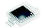
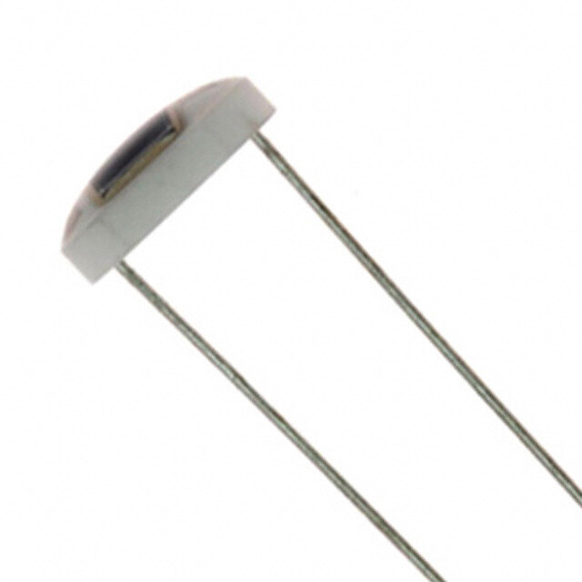
ICGOO电子元器件商城为您提供BPW 34 S-Z由OSRAM SYLVANIA设计生产,在icgoo商城现货销售,并且可以通过原厂、代理商等渠道进行代购。 BPW 34 S-Z价格参考。OSRAM SYLVANIABPW 34 S-Z封装/规格:光学传感器 - 光电二极管, Photodiode 850nm 20ns 120° 2-SMD, Gull Wing。您可以下载BPW 34 S-Z参考资料、Datasheet数据手册功能说明书,资料中有BPW 34 S-Z 详细功能的应用电路图电压和使用方法及教程。
OSRAM Opto Semiconductors Inc. 的 BPW 34 S-Z 是一款高灵敏度硅 PIN 光电二极管,属于光学传感器中的光电二极管类别。该器件对可见光和近红外光(波长范围约 430 nm 至 1100 nm,峰值响应在 880 nm 左右)具有优异的响应性能,响应速度快、线性度高,且暗电流低,适合精密光检测应用。

BPW 34 S-Z 广泛应用于多种光电检测场景。常见用途包括:
- 光强度检测:用于自动照明系统、环境光传感器中,实现灯光的智能调节;
- 工业自动化:在光电开关、物体检测、位置传感等系统中作为接收元件;
- 消费电子:应用于智能手机、平板电脑中的亮度自动调节功能;
- 光学编码器:用于电机控制或旋转位置检测;
- 医疗设备:如脉搏血氧仪、光学测量仪器中的光信号接收;
- 安全与监控系统:配合红外发射源,用于烟雾探测、入侵检测等;
- 太阳能相关设备:用于光照强度监测或太阳能跟踪系统。

该型号采用表面贴装封装(SMD),便于自动化生产,同时具备良好的稳定性和可靠性,适用于要求紧凑设计和高性能的现代电子设备。由于其宽光谱响应和高性价比,BPW 34 S-Z 在工业、消费和医疗领域均有广泛应用。
| 参数 | 数值 |
| 产品目录 | |
| 描述 | PHOTODIODE SMT光电二极管 PHOTODIODE, SMT |
| 产品分类 | |
| 品牌 | OSRAM Opto Semiconductors |
| 产品手册 | |
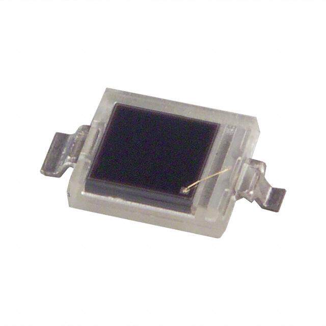
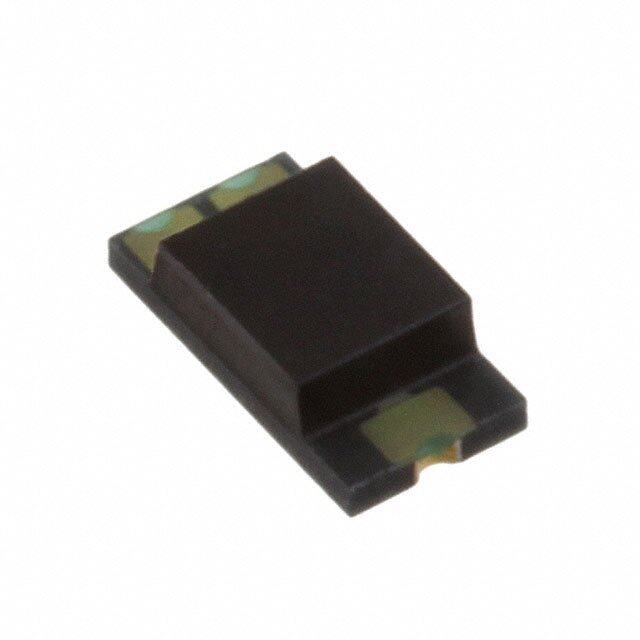
| 产品图片 |
|
| rohs | 符合RoHS无铅 / 符合限制有害物质指令(RoHS)规范要求 |
| 产品系列 | 光电二极管,OSRAM Opto Semiconductors BPW 34 S-Z- |
| 数据手册 | |
| 产品型号 | BPW 34 S-Z |
| 上升时间 | 20 ns |
| 下降时间 | 20 ns |
| 不同nm时的响应度 | - |
| 二极管类型 | 引脚 |
| 产品 | PIN Photodiodes |
| 产品目录绘图 |
|
| 产品目录页面 | |
| 产品种类 | 光电二极管 |
| 光电流 | 80 uA |
| 其它名称 | 475-2659-1 |
| 功率耗散 | 150 mW |
| 半强度角度 | 60 deg |
| 反向电压 | 32 V |
| 响应时间 | 20ns |
| 响应率 | 0.62 A/W |
| 商标 | OSRAM Opto Semiconductors |
| 噪声等效功率-NEP | 4.1E-14 W/sqrt Hz |
| 安装风格 | SMD/SMT |
| 封装 | Reel |
| 封装/外壳 | 2-SMD,Z形弯曲d |
| 封装/箱体 | DIL-SMT-2 |
| 峰值波长 | 850 nm |
| 工作温度 | -40°C ~ 100°C |
| 工厂包装数量 | 1500 |
| 暗电流 | 2 nA |
| 最大工作温度 | + 100 C |
| 最大暗电流 | 30 nA |
| 最小工作温度 | - 40 C |
| 有效面积 | 2.65mm x 2.65mm (7mm²) |
| 标准包装 | 1 |
| 正向电流 | 100 mA |
| 波长 | 850nm |
| 电压-DC反向(Vr)(最大值) | 32V |
| 电流-暗(典型值) | 2nA |
| 视角 | 120° |
| 零件号别名 | Q65110A1209 |
| 频谱范围 | 400nm ~ 1100nm |
| 颜色-增强 | - |


- 商务部:美国ITC正式对集成电路等产品启动337调查
- 曝三星4nm工艺存在良率问题 高通将骁龙8 Gen1或转产台积电
- 太阳诱电将投资9.5亿元在常州建新厂生产MLCC 预计2023年完工
- 英特尔发布欧洲新工厂建设计划 深化IDM 2.0 战略
- 台积电先进制程称霸业界 有大客户加持明年业绩稳了
- 达到5530亿美元!SIA预计今年全球半导体销售额将创下新高
- 英特尔拟将自动驾驶子公司Mobileye上市 估值或超500亿美元
- 三星加码芯片和SET,合并消费电子和移动部门,撤换高东真等 CEO
- 三星电子宣布重大人事变动 还合并消费电子和移动部门
- 海关总署:前11个月进口集成电路产品价值2.52万亿元 增长14.8%
PDF Datasheet 数据手册内容提取
Silizium-PIN-Fotodiode; in SMT und als Reverse Gullwing Silicon PIN Photodiode; in SMT and as Reverse Gullwing BPW 34, BPW 34 S, BPW 34 S (E9087) BPW34 BPW34S BPW34S (E9087) Wesentliche Merkmale Features • Speziell geeignet für Anwendungen im Bereich (cid:127) Especially suitable for applications from von 400 nm bis 1100 nm 400 nm to 1100 nm (cid:127) Kurze Schaltzeit (typ. 20 ns) (cid:127) Short switching time (typ. 20 ns) (cid:127) DIL-Plastikbauform mit hoher Packungsdichte (cid:127) DIL plastic package with high packing density (cid:127) BPW 34 S/(E9087): geeignet für Vapor-Phase (cid:127) BPW 34 S/(E9087): suitable for vapor-phase Löten und IR-Reflow Löten (JEDEC level 4) and IR-reflow soldering (JEDEC level 4) Anwendungen Applications (cid:127) Lichtschranken für Gleich- und (cid:127) Photointerrupters Wechsellichtbetrieb (cid:127) IR remote controls (cid:127) IR-Fernsteuerungen (cid:127) Industrial electronics (cid:127) Industrieelektronik (cid:127) For control and drive circuits (cid:127) „Messen/Steuern/Regeln“ Typ Bestellnummer Type Ordering Code BPW 34 Q62702-P73 BPW 34 S Q62702-P1602 BPW 34 S (E9087) Q62702-P1790 2003-02-04 1
BPW 34, BPW 34 S, BPW 34 S (E9087) Grenzwerte Maximum Ratings Bezeichnung Symbol Wert Einheit Parameter Symbol Value Unit BPW 34 S BPW 34 BPW 34 S (E9087) Betriebs- und Lagertemperatur T ; T – 40 … + 100 – 40 … + 85 °C op stg Operating and storage temperature range Sperrspannung V 32 V R Reverse voltage Verlustleistung, T = 25 °C P 150 mW A tot Total power dissipation Kennwerte (T = 25 °C, Normlicht A, T = 2856 K) A Characteristics (T = 25 °C, standard light A, T = 2856 K) A Bezeichnung Symbol Wert Einheit Parameter Symbol Value Unit Fotoempfindlichkeit, V = 5 V S 80 (≥ 50) nA/Ix R Spectral sensitivity Wellenlänge der max. Fotoempfindlichkeit λ 850 nm S max2003-02-04 Wavelength of max. sensitivity Spektraler Bereich der Fotoempfindlichkeit λ 400 … 1100 nm S = 10% von S max Spectral range of sensitivity S = 10% of S max Bestrahlungsempfindliche Fläche A 7.00 mm2 Radiant sensitive area Abmessung der bestrahlungsempfindlichen L × B 2.65 × 2.65 mm × mm Fläche Dimensions of radiant sensitive area L × W Halbwinkel ϕ ± 60 Grad Half angle deg. Dunkelstrom, V = 10 V I 2 (≤ 30) nA R R Dark current Spektrale Fotoempfindlichkeit, λ = 850 nm S 0.62 A/W λ Spectral sensitivity Quantenausbeute, λ = 850 nm η 0.90 Electrons Quantum yield Photon 2003-02-04 2
BPW 34, BPW 34 S, BPW 34 S (E9087) Kennwerte (T = 25 °C, Normlicht A, T = 2856 K) A Characteristics (T = 25 °C, standard light A, T = 2856 K) (cont’d) A Bezeichnung Symbol Wert Einheit Parameter Symbol Value Unit Leerlaufspannung, E = 1000 Ix V 365 (≥ 300) mV v O Open-circuit voltage Kurzschlußstrom, E = 1000 Ix I 80 µA v SC Short-circuit current Anstiegs- und Abfallzeit des Fotostromes t, t 20 ns r f Rise and fall time of the photocurrent R = 50 Ω; V = 5 V; λ = 850 nm; I = 800 µA L R p Durchlaßspannung, I = 100 mA, E = 0 V 1.3 V F F Forward voltage Kapazität, V = 0 V, f = 1 MHz, E = 0 C 72 pF R 0 Capacitance Temperaturkoeffizient von V TC – 2.6 mV/K O V Temperature coefficient of V O Temperaturkoeffizient von I TC 0.18 %/K SC I Temperature coefficient of I SC Rauschäquivalente Strahlungsleistung NEP 4.1 × 10– 14 W ------------ Noise equivalent power Hz V = 10 V, λ = 850 nm R Nachweisgrenze, V = 10 V, λ = 850 nm D* 6.6 × 10¹² R cm× Hz Detection limit -------------------------- W 2003-02-04 3
BPW 34, BPW 34 S, BPW 34 S (E9087) Relative Spectral Sensitivity Photocurrent I = f (E ), V = 5 V Total Power Dissipation P v R S = f (λ) Open-Circuit Voltage V = f (E ) P = f (T ) rel O v tot A 100 OHF00078 103 OHF01066104 160 OHF00958 µA mV mW Srel % ΙP VO Ptot140 80 102 103 120 V O 100 60 101 102 80 Ι P 40 60 100 101 40 20 20 0 10-1 100 0 400 500 600 700 800 900 nm 1100 100 101 102 103 lx 104 0 20 40 60 80 ˚C 100 λ EV TA Dark Current Capacitance Dark Current I = f (V ), E = 0 C = f (V ), f = 1 MHz, E = 0 I = f (T ), V = 10 V, E = 0 R R R R A R 4000 OHF00080 100 OHF00081 103 OHF00082 ΙR pA C pF ΙR nA 80 3000 102 70 60 2000 50 101 40 30 1000 100 20 10 0 0 10-1 0 5 10 15 V 20 10-2 10-1 100 101 V 102 0 20 40 60 80 ˚C 100 VR VR TA Directional Characteristics S = f (ϕ) rel 40 30 20 10 0 OHF01402 ϕ 1.0 50 0.8 60 0.6 70 0.4 80 0.2 0 90 100 1.0 0.8 0.6 0.4 0 20 40 60 80 100 120 2003-02-04 4
BPW 34, BPW 34 S, BPW 34 S (E9087) Maßzeichnung Package Outlines BPW34 5.4 (0.213) Cathode marking 4.9 (0.193) 4.0 (0.157) 4.5 (0.177) Chip position 3.7 (0.146) 4.3 (0.169) 0.6 (0.024) 0.4 (0.016) 2 (0.047)7 (0.028) 0.8 (0.031) 0.6 (0.024) 0.6 (0.024) 0.4 (0.016) 2.2 (0.087) 1.9 (0.075) 1.0. 0.6 (0.024) 0.6 (0.024) 8) 8) 3 1 1 1 0.4 (0.016) 0.4 (0.016) 0. 0. 0.5 (0.020) 0.35 (0.014) 3.5 ( 3.0 ( 0.3 (0.012) 0.2 (0.008) 0.8 (0.031) 0 ... 5˚ 0.6 (0.024) 1)5) 75 00 0.0. 1.8 (1.4 ( 5.08 (0.200) spacing Photosensitive area 2.65 (0.104) x 2.65 (0.104) GEOY6643 BPW34S Chip position 7)3) 2) 44 1 1.1 (0.043) 1.2 (0.01.1 (0.0 0...0.1(0...0.004) 0.3 (0.0 0.9 (0.035) 5˚ 08) 04) 6.7 (0.264) 0... 0.0 0.0 6.2 (0.244) 2 ( 1 ( 0. 0. 4.5 (0.177) 4.3 (0.169) 1.8 (0.071)±0.2 (0.008) 7)6) 54 0.9 (0.035)0.7 (0.028) 1.7 (0.067)1.5 (0.059) 4.0 (0.13.7 (0.1 Photosensitive area Cathode lead 2.65 (0.104) x 2.65 (0.104) GEOY6863 Maße werden wie folgt angegeben: mm (inch) / Dimensions are specified as follows: mm (inch). 2003-02-04 5
BPW 34, BPW 34 S, BPW 34 S (E9087) BPW34S (E9087) Chip position 7)3) 4) 2) 1.1 (0.043) 1.2 (0.041.1 (0.04 0...0.1(0...0.00 0.3 (0.01 0.9 (0.035) 5˚ 8) 4) 0... 0.00 0.00 6.7 (0.264) 2 ( 1 ( 0. 0. 6.2 (0.244) 4.5 (0.177) 4.3 (0.169) 1.8 (0.071)±0.2 (0.008) 7)6) 54 0.9 (0.035)0.7 (0.028) 1.7 (0.067)1.5 (0.059) 4.0 (0.13.7 (0.1 Photosensitive area Cathode lead 2.65 (0.104) x 2.65 (0.104) GEOY6916 Maße werden wie folgt angegeben: mm (inch) / Dimensions are specified as follows: mm (inch). Published by OSRAM Opto Semiconductors GmbH & Co. OHG Wernerwerkstrasse 2, D-93049 Regensburg © All Rights Reserved. Attention please! The information describes the type of component and shall not be considered as assured characteristics. Terms of delivery and rights to change design reserved. Due to technical requirements components may contain dangerous substances. For information on the types in question please contact our Sales Organization. Packing Please use the recycling operators known to you. We can also help you – get in touch with your nearest sales office. By agreement we will take packing material back, if it is sorted. You must bear the costs of transport. For packing material that is returned to us unsorted or which we are not obliged to accept, we shall have to invoice you for any costs incurred. Components used in life-support devices or systems must be expressly authorized for such purpose! Critical components 1 , may only be used in life-support devices or systems 2 with the express written approval of OSRAM OS. 1 A critical component is a component usedin a life-support device or system whose failure can reasonably be expected to cause the failure of that life-support device or system, or to affect its safety or effectiveness of that device or system. 2 Life support devices or systems are intended (a) to be implanted in the human body, or (b) to support and/or maintain and sustain human life. If they fail, it is reasonable to assume that the health of the user may be endangered. 2003-02-04 6