ICGOO在线商城 > BD4959G-TR
 Datasheet下载
- 型号: BD4959G-TR
- 制造商: ROHM Semiconductor
- 库位|库存: xxxx|xxxx
- 要求:
| 数量阶梯 | 香港交货 | 国内含税 |
| +xxxx | $xxxx | ¥xxxx |
查看当月历史价格
查看今年历史价格
BD4959G-TR产品简介:
ICGOO电子元器件商城为您提供BD4959G-TR由ROHM Semiconductor设计生产,在icgoo商城现货销售,并且可以通过原厂、代理商等渠道进行代购。 提供BD4959G-TR价格参考¥1.01-¥1.40以及ROHM SemiconductorBD4959G-TR封装/规格参数等产品信息。 你可以下载BD4959G-TR参考资料、Datasheet数据手册功能说明书, 资料中有BD4959G-TR详细功能的应用电路图电压和使用方法及教程。
| 参数 | 数值 |
| 产品目录 | 集成电路 (IC) |
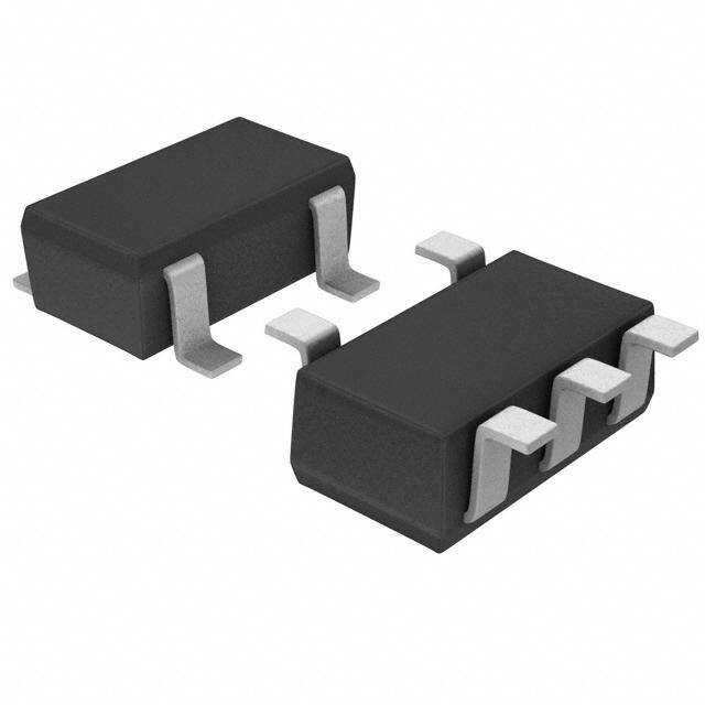
| 描述 | IC RESET CMOS 5.9V 5SSOP |
| 产品分类 | |
| 品牌 | Rohm Semiconductor |
| 数据手册 | |
| 产品图片 |
|
| 产品型号 | BD4959G-TR |
| rohs | 无铅 / 符合限制有害物质指令(RoHS)规范要求 |
| 产品系列 | BD49xxx |
| 产品培训模块 | http://www.digikey.cn/PTM/IndividualPTM.page?site=cn&lang=zhs&ptm=30334 |
| 供应商器件封装 | 5-SSOP |
| 其它名称 | BD4959GDKR |
| 包装 | Digi-Reel® |
| 受监控电压数 | 1 |
| 复位 | 低有效 |
| 复位超时 | - |
| 安装类型 | 表面贴装 |
| 封装/外壳 | 6-TFSOP(0.063",1.60mm 宽),5 引线 |
| 工作温度 | -40°C ~ 105°C |
| 标准包装 | 1 |
| 电压-阈值 | 5.9V |
| 类型 | 简单复位/加电复位 |
| 输出 | 推挽式,图腾柱 |


- 商务部:美国ITC正式对集成电路等产品启动337调查
- 曝三星4nm工艺存在良率问题 高通将骁龙8 Gen1或转产台积电
- 太阳诱电将投资9.5亿元在常州建新厂生产MLCC 预计2023年完工
- 英特尔发布欧洲新工厂建设计划 深化IDM 2.0 战略
- 台积电先进制程称霸业界 有大客户加持明年业绩稳了
- 达到5530亿美元!SIA预计今年全球半导体销售额将创下新高
- 英特尔拟将自动驾驶子公司Mobileye上市 估值或超500亿美元
- 三星加码芯片和SET,合并消费电子和移动部门,撤换高东真等 CEO
- 三星电子宣布重大人事变动 还合并消费电子和移动部门
- 海关总署:前11个月进口集成电路产品价值2.52万亿元 增长14.8%


.jpg)


PDF Datasheet 数据手册内容提取
Datasheet Voltage Detector IC Series Standard CMOS Voltage Detector IC BD48xxx series BD49xxx series ●General Description ●Key Specifications ROHM’s BD48xxx and BD49xxx series are highly (cid:1) Detection voltage: 2.3V to 6.0V (Typ.), accurate, low-current Voltage Detector IC series. The 0.1V steps family includes BD48xxx devices with N-channel open (cid:1) High accuracy detection voltage: ±1.0% drain output and BD49xxx devices with CMOS output. (cid:1) Ultra-low current consumption: 0.9µA (Typ.) The devices are available for specific detection voltages (cid:1) Operating temperature range: -40°C to +105°C ranging from 2.3V to 6.0V in increments of 0.1V. ●Package SSOP5: 2.90mm x 2.80mm x 1.25mm ●Features (cid:1) High accuracy detection SSOP3: 2.92mm x 2.80mm x 1.25mm (cid:1) Ultra-low current consumption (cid:1) Two output types (Nch open drain and CMOS output) VSOF5: 1.60 mm x 1.60mm x 0.60mm (cid:1) Wide Operating temperature range (cid:1) Very small and low height package ●Applications (cid:1) Package SSOP5 is similar to SOT-23-5 (JEDEC) Circuits using microcontrollers or logic circuits that (cid:1) Package SSOP3 is similar to SOT-23-3 (JEDEC) require a reset. ●Typical Application Circuit V DD1 V DD2 V DD1 RL BD49xxx RST Mi cr o Micro controller BD48xxx RST con t roller CL C L ( Capacitor for ( Capacitor for noise filtering) noise filtering) GND GND (Open Drain Output type) (CMOS Output type) BD48xxx series BD49xxx series ○Product structure:Silicon monolithic integrated circuit ○This product is not designed for protection against radioactive rays .w ww.rohm.com TSZ02201-0R7R0G300030-1-2 © 2013 ROHM Co., Ltd. All rights reserved. 1/15 TSZ22111・14・001 22.May.2013.Rev.008
Datasheet BD48xxx series BD49xxx series ●Connection Diagram SSOP5 N . C . N .C . VSOF5 VDD GND 5 4 Marking Lot. No Marking Lot. No 1 2 3 VOUT S UB N.C VOUT VDD GND TOP VIEW TOP VIEW ●Pin Descriptions SSOP5 VSOF5 PIN No. Symbol Function PIN No. Symbol Function 1 VOUT Reset Output 1 VOUT Reset Output 2 VDD Power Supply Voltage 2 SUB Substrate* 3 GND GND 3 N.C. Unconnected Terminal 4 N.C. Unconnected Terminal 4 GND GND 5 N.C. Unconnected Terminal 5 VDD Power Supply Voltage *Connect the substrate to GND. SSOP3(1pin GND) SSOP3(3pin GND) VDD GND 3 3 2 Marking Lot. No Marking Lot. No 1 2 1 2 GND VOUT VOUT VDD TOP VIEW TOP VIEW ●Pin Descriptions SSOP3-1 SSOP3-2 PIN No. Symbol Function PIN No. Symbol Function 1 GND GND 1 VOUT Reset Output 2 VOUT Reset Output 2 VDD Power Supply Voltage 3 VDD Power Supply Voltage 3 GND GND (cid:2) Ordering Information B D x x x x x x - T R Part Output Type Package1 Reset Voltage Value Package2 Packaging and Number 48 : Open Drain 23 : 2.3V forming specification 49 : CMOS 0.1V step Embossed tape and reel 60 : 6.0V TR :The pin number 1is the upper right :SSOP5 :VSOF5 TL :The pin number 1is Package1 Package2 Package name the upper left E G SSOP5 :SSOP3-1 K G SSOP3(1pin GND) :SSOP3-2 L G SSOP3(3pin GND) Blank FVE VSOF5 Blank G SSOP5 Note: When ordering new SSOP5, select “E” for Package 1 and “G” for Package 2. www.rohm.com TSZ02201-0R7R0G300030-1-2 © 2013 ROHM Co., Ltd. All rights reserved. 2/15 TSZ22111・15・001 22.May.2013.Rev.008
Datasheet BD48xxx series BD49xxx series SSOP5 <Tape and Reel information> 2.9–0.2 4(cid:176) +-46(cid:176)(cid:176) Tape Embossed carrier tape 5 4 Quantity 3000pcs –2.80.2 +0.21.6-0.1 Min. Dofi rfeecetdion T(RTreheel odnir ethcetio lenf tis h tahned 1 apnind oyfo pur opduull cot uist tahte t htaep uep opne rt hrieg hritg whth heann ydou hold ) 1 2 3 0.2 0.13+-00.0.035 1pin Max. 1.25 +0.05 –1.10.05 –0.050.05 0.95 0.01.42-0.04 Direction of feed (Unit : mm) Reel * Order quantity needs to be multiple of the minimum quantity. VSOF5 1.6– 0.05 1.0– 0.05 X 5 4 0.2MA –1.60.05 –1.20.05(MAX 1.28 include BURR) 1 2 3 0.13– 0.05 X A M 0.6 0.5 0.22– 0.05 (Unit : mm) SSOP3 2.92±0.1 4°±4° 3 L ±2.80.15 ±1.60.1 ±0.450.15 1 2 0.15±0.05 1.25MAX ±1.10.05 XXXXXX XXXXXX XXXXXX XXXXXX XXXXXX 0.95 0.4±0.1 1.9±0.1 www.rohm.com TSZ02201-0R7R0G300030-1-2 © 2013 ROHM Co., Ltd. All rights reserved. 3/15 TSZ22111・15・001 22.May.2013.Rev.008
Datasheet BD48xxx series BD49xxx series ●Lineup Table 1. Lineup for VSOF5 and SSOP5 Package Package Type VSOF5 or SSOP5 SSOP5 Output Type Open Drain CMOS Open Drain CMOS Detection Marking Part Number Marking Part Number Marking Part Number Marking Part Number Voltage 6.0V EW BD4860 GW BD4960 Cm BD48E60 Ff BD49E60 5.9V EV BD4859 GV BD4959 Ck BD48E59 Fe BD49E59 5.8V EU BD4858 GU BD4958 Ch BD48E58 Fd BD49E58 5.7V ET BD4857 GT BD4957 Cg BD48E57 Fc BD49E57 5.6V ES BD4856 GS BD4956 Cf BD48E56 Fb BD49E56 5.5V ER BD4855 GR BD4955 Ce BD48E55 Fa BD49E55 5.4V EQ BD4854 GQ BD4954 Cd BD48E54 Ey BD49E54 5.3V EP BD4853 GP BD4953 Cc BD48E53 Er BD49E53 5.2V EN BD4852 GN BD4952 Cb BD48E52 Ep BD49E52 5.1V EM BD4851 GM BD4951 Ca BD48E51 En BD49E51 5.0V EL BD4850 GL BD4950 By BD48E50 Em BD49E50 4.9V EK BD4849 GK BD4949 Br BD48E49 Ek BD49E49 4.8V EJ BD4848 GJ BD4948 Bp BD48E48 Eh BD49E48 4.7V EH BD4847 GH BD4947 Bn BD48E47 Eg BD49E47 4.6V EG BD4846 GG BD4946 Bm BD48E46 Ef BD49E46 4.5V EF BD4845 GF BD4945 Bk BD48E45 Ee BD49E45 4.4V EE BD4844 GE BD4944 Bh BD48E44 Ed BD49E44 4.3V ED BD4843 GD BD4943 Bg BD48E43 Ec BD49E43 4.2V EC BD4842 GC BD4942 Bf BD48E42 Eb BD49E42 4.1V EB BD4841 GB BD4941 Be BD48E41 Ea BD49E41 4.0V EA BD4840 GA BD4940 Bd BD48E40 Dy BD49E40 3.9V DV BD4839 FV BD4939 Bc BD48E39 Dr BD49E39 3.8V DU BD4838 FU BD4938 Bb BD48E38 Dp BD49E38 3.7V DT BD4837 FT BD4937 Ba BD48E37 Dn BD49E37 3.6V DS BD4836 FS BD4936 Ay BD48E36 Dm BD49E36 3.5V DR BD4835 FR BD4935 Ar BD48E35 Dk BD49E35 3.4V DQ BD4834 FQ BD4934 Ap BD48E34 Dh BD49E34 3.3V DP BD4833 FP BD4933 An BD48E33 Dg BD49E33 3.2V DN BD4832 FN BD4932 Am BD48E32 Df BD49E32 3.1V DM BD4831 FM BD4931 Ak BD48E31 De BD49E31 3.0V DL BD4830 FL BD4930 Ah BD48E30 Dd BD49E30 2.9V DK BD4829 FK BD4929 Ag BD48E29 Dc BD49E29 2.8V DJ BD4828 FJ BD4928 Af BD48E28 Db BD49E28 2.7V DH BD4827 FH BD4927 Ae BD48E27 Da BD49E27 2.6V DG BD4826 FG BD4926 Ad BD48E26 Cy BD49E26 2.5V DF BD4825 FF BD4925 Ac BD48E25 Cr BD49E25 2.4V DE BD4824 FE BD4924 Ab BD48E24 Cp BD49E24 2.3V DD BD4823 FD BD4923 Aa BD48E23 Cn BD49E23 www.rohm.com TSZ02201-0R7R0G300030-1-2 © 2013 ROHM Co., Ltd. All rights reserved. 4/15 TSZ22111・15・001 22.May.2013.Rev.008
Datasheet BD48xxx series BD49xxx series ●●●●Lineup - continued Table 2. Lineup for SSOF3(1pin GND) and SSOP3(3pin GND) Package Package Type SSOP3(1pin GND) SSOP3(3pin GND) Output Type Open Drain CMOS Open Drain CMOS Detection Marking Part Number Marking Part Number Marking Part Number Marking Part Number Voltage 6.0V Cm BD48K60 Ff BD49K60 Kb BD48L60 Np BD49L60 5.9V Ck BD48K59 Fe BD49K59 Ka BD48L59 Nn BD49L59 5.8V Ch BD48K58 Fd BD49K58 Hy BD48L58 Nm BD49L58 5.7V Cg BD48K57 Fc BD49K57 Hr BD48L57 Nk BD49L57 5.6V Cf BD48K56 Fb BD49K56 Hp BD48L56 Nh BD49L56 5.5V Ce BD48K55 Fa BD49K55 Hn BD48L55 Ng BD49L55 5.4V Cd BD48K54 Ey BD49K54 Hm BD48L54 Nf BD49L54 5.3V Cc BD48K53 Er BD49K53 Hk BD48L53 Ne BD49L53 5.2V Cb BD48K52 Ep BD49K52 Hh BD48L52 Nd BD49L52 5.1V Ca BD48K51 En BD49K51 Hg BD48L51 Nc BD49L51 5.0V By BD48K50 Em BD49K50 Hf BD48L50 Nb BD49L50 4.9V Br BD48K49 Ek BD49K49 He BD48L49 Na BD49L49 4.8V Bp BD48K48 Eh BD49K48 Hd BD48L48 My BD49L48 4.7V Bn BD48K47 Eg BD49K47 Hc BD48L47 Mr BD49L47 4.6V Bm BD48K46 Ef BD49K46 Hb BD48L46 Mp BD49L46 4.5V Bk BD48K45 Ee BD49K45 Ha BD48L45 Mn BD49L45 4.4V Bh BD48K44 Ed BD49K44 Gy BD48L44 Mm BD49L44 4.3V Bg BD48K43 Ec BD49K43 Gr BD48L43 Mk BD49L43 4.2V Bf BD48K42 Eb BD49K42 Gp BD48L42 Mh BD49L42 4.1V Be BD48K41 Ea BD49K41 Gn BD48L41 Mg BD49L41 4.0V Bd BD48K40 Dy BD49K40 Gm BD48L40 Mf BD49L40 3.9V Bc BD48K39 Dr BD49K39 Gk BD48L39 Me BD49L39 3.8V Bb BD48K38 Dp BD49K38 Gh BD48L38 Md BD49L38 3.7V Ba BD48K37 Dn BD49K37 Gg BD48L37 Mc BD49L37 3.6V Ay BD48K36 Dm BD49K36 Gf BD48L36 Mb BD49L36 3.5V Ar BD48K35 Dk BD49K35 Ge BD48L35 Ma BD49L35 3.4V Ap BD48K34 Dh BD49K34 Gd BD48L34 Ky BD49L34 3.3V An BD48K33 Dg BD49K33 Gc BD48L33 Kr BD49L33 3.2V Am BD48K32 Df BD49K32 Gb BD48L32 Kp BD49L32 3.1V Ak BD48K31 De BD49K31 Ga BD48L31 Kn BD49L31 3.0V Ah BD48K30 Dd BD49K30 Fy BD48L30 Km BD49L30 2.9V Ag BD48K29 Dc BD49K29 Fr BD48L29 Kk BD49L29 2.8V Af BD48K28 Db BD49K28 Fp BD48L28 Kh BD49L28 2.7V Ae BD48K27 Da BD49K27 Fn BD48L27 Kg BD49L27 2.6V Ad BD48K26 Cy BD49K26 Fm BD48L26 Kf BD49L26 2.5V Ac BD48K25 Cr BD49K25 Fk BD48L25 Ke BD49L25 2.4V Ab BD48K24 Cp BD49K24 Fh BD48L24 Kd BD49L24 2.3V Aa BD48K23 Cn BD49K23 Fg BD48L23 Kc BD49L23 www.rohm.com TSZ02201-0R7R0G300030-1-2 © 2013 ROHM Co., Ltd. All rights reserved. 5/15 TSZ22111・15・001 22.May.2013.Rev.008
Datasheet BD48xxx series BD49xxx series ●Absolute Maximum Ratings Parameter Symbol Limits Unit Power Supply Voltage V -GND -0.3 to +10 V DD Nch Open Drain Output GND-0.3 to +10 Output Voltage V V OUT CMOS Output GND-0.3 to V +0.3 DD Output Current Io 70 mA SSOP5 *1*4 540 Power SSOP3 *2*4 Pd 700 mW Dissipation VSOF5 *3*4 210 Operating Temperature Topr -40 to +105 °C Ambient Storage Temperature Tstg -55 to +125 °C *1 Reduced by 5.4mW/°C when used over 25°C. *2 Reduced by 7.0mW/°C when used over 25°C. *3 Reduced by 2.1mW/°C when used over 25°C. *4 When mounted on ROHM standard circuit board (70mm×70mm×1.6mm, glass epoxy board). ●Electrical Characteristics (Unless Otherwise Specified, Ta=-40 to 105°C) Limit Parameter Symbol Condition Unit Min. Typ. Max. V (T) V (T) RL=470kΩ, VDD=H(cid:3)L *1 DET VDET(T) DET ×0.99 ×1.01 Ta=+25°C 2.475 2.5 2.525 VDET=2.5V Ta=-40°C to 85°C 2.418 - 2.584 Ta=85°C to 105°C 2.404 - 2.597 Ta=+25°C 2.970 3.0 3.030 VDET=3.0V Ta=-40°C to 85°C 2.901 - 3.100 Ta=85°C to 105°C 2.885 - 3.117 Detection Voltage VDET Ta=+25°C 3.267 3.3 3.333 V VDET=3.3V Ta=-40°C to 85°C 3.191 - 3.410 Ta=85°C to 105°C 3.173 - 3.428 Ta=+25°C 4.158 4.2 4.242 VDET=4.2V Ta=-40°C to 85°C 4.061 - 4.341 Ta=85°C to 105°C 4.039 - 4.364 Ta=+25°C 4.752 4.8 4.848 VDET=4.8V Ta=-40°C to 85°C 4.641 - 4.961 Ta=85°C to 105°C 4.616 - 4.987 Output Delay Time “L(cid:3)H” tPLH CL=100pF RL=100kΩ *2 - - 100 µs Vout=GND(cid:3)50% V =2.3-3.1V - 0.51 1.53 DET V =3.2-4.2V - 0.56 1.68 Circuit Current when ON ICC1 VDD=VDET-0.2V *1 DET µA V =4.3-5.2V - 0.60 1.80 DET V =5.3-6.0V - 0.66 1.98 DET V =2.3-3.1V - 0.75 2.25 DET V =3.2-4.2V - 0.80 2.40 Circuit Current when OFF ICC2 VDD=VDET+2.0V *1 DET µA V =4.3-5.2V - 0.85 2.55 DET V =5.3-6.0V - 0.90 2.70 DET VOL≤0.4V, Ta=25 to 105°C, RL=470kΩ 0.95 - - Operating Voltage Range VOPL V VOL≤0.4V, Ta=-40 to 25°C, RL=470kΩ 1.20 - - VDET(T) : Standard Detection Voltage(2.3V to 6.0V, 0.1V step) RL: Pull-up resistor to be connected between VOUT and power supply. CL: Capacitor to be connected between VOUT and GND. Design Guarantee. (Outgoing inspection is not done on all products.) *1 Guaranteed at Ta=25°C. *2 tPLH:VDD=(VDET typ.-0.5V)(cid:3)(VDET typ.+0.5V) www.rohm.com TSZ02201-0R7R0G300030-1-2 © 2013 ROHM Co., Ltd. All rights reserved. 6/15 TSZ22111・15・001 22.May.2013.Rev.008
Datasheet BD48xxx series BD49xxx series ●Electrical Characteristics (Unless Otherwise Specified, Ta=-40 to 105°C) - continued Limit Parameter Symbol Condition Unit Min. Typ. Max. VDD=1.5V, ISINK = 0.4 mA, VDET=2.3-6.0V - - 0.5 ‘Low’Output Voltage (Nch) VOL V VDD=2.4V, ISINK = 2.0 mA, VDET=2.7-6.0V - - 0.5 VDD=4.8V, ISOURCE=0.7 mA, VDET(2.3V to 4.2V) VDD-0.5 - - ‘High’Output Voltage (Pch) VOH VDD=6.0V, ISOURCE=0.9 mA,VDET(4.3V to 5.2V) VDD-0.5 - - V (BD49Exxx Series) VDD=8.0V, ISOURCE=1.1 mA,VDET(5.3V to 6.0V) VDD-0.5 - - Leak Current when OFF Ileak VDD=VDS=10V *1 - - 0.1 µA (BD48xxx Series) Detection Voltage Ta=-40°C to 105°C V /∆T - ±100 ±360 ppm/°C DET Temperature coefficient (Designed Guarantee) Hysteresis Voltage ∆VDET VDD=L(cid:3)H(cid:3)L, RL=470kΩ VDET×0.03 VDET×0.05 VDET×0.08 V VDET(T) : Standard Detection Voltage(2.3V to 6.0V, 0.1V step) RL: Pull-up resistor to be connected between VOUT and power supply. CL: Capacitor to be connected between VOUT and GND. Design Guarantee. (Outgoing inspection is not done on all products.) *1 Guaranteed at Ta=25°C. www.rohm.com TSZ02201-0R7R0G300030-1-2 © 2013 ROHM Co., Ltd. All rights reserved. 7/15 TSZ22111・15・001 22.May.2013.Rev.008
Datasheet BD48xxx series BD49xxx series ●Block Diagrams VDD VOUT Vref GND Fig.1 BD48xxx series VDD VOUT Vref GND Fig.2 BD49xxx series www.rohm.com TSZ02201-0R7R0G300030-1-2 © 2013 ROHM Co., Ltd. All rights reserved. 8/15 TSZ22111・15・001 22.May.2013.Rev.008
Datasheet BD48xxx series BD49xxx series ●Typical Performance Curves 2.0 20 【B【DB48D4428Gx4/F2V】E 】 mA] 【【BBDD484482xG42/F】V E】 :µ I[A]DD1.5 【BD49x42】 :NT I[OL 15 【BD49x42】 T E N R E R R1.0 U 10 R C V =2.4V CU T DD U T P CUI0.5 UT 5 R O CI W" VDD=1.2V O 0.0 L 0 " 0 1 2 3 4 5 6 7 8 9 10 0.0 0.5 1.0 1.5 2.0 2.5 VDD SUPPLY VOLTAGE :VDD[V] DRAIN-SOURCE VOLTAGE : VDS[V] Fig.3 Circuit Current Fig.4 “Low” Output Current 45 A] 9 m 40 【【BDBD494492x4G2/F】V E】 【【BDB4D84482xG4/2F】VE 】 [H V] 8 : IO 35 [UT 7 【BD49x42】 T VO EN 30 :E 6 R 25 G R A 5 U T T C 20 VDD=8.0V VOL 4 PU 15 T 3 OUT 10 VDD=6.0V TPU 2 Ta=25℃ U H" 5 O 1 G VDD=4.8V Ta=25℃ HI 0 0 " 0 1 2 3 4 5 6 0 0.5 1 1.5 2 2.5 3 3.5 4 4.5 5 5.5 DRAIN-SOURCE VOLTAGE : VDS[V] VDD SUPPLY VOLTAGE :VDD[V] Fig.5 “High” Output Current Fig.6 I/O Characteristics www.rohm.com TSZ02201-0R7R0G300030-1-2 © 2013 ROHM Co., Ltd. All rights reserved. 9/15 TSZ22111・15・001 22.May.2013.Rev.008
Datasheet BD48xxx series BD49xxx series ●Typical Performance Curves – continued 1.0 : V[V]OUT 0.8 【【【B【BBD BDD4D4489844xx8244xG224/】】2Fx V 】E 】 V[V] DET 55..04 【【【【B BBBDDDD444489884xxx2444G222/】】xF V 】E 】 GE GE: Low to High(VDET+∆VDET) OLTA 0.6 OLTA 4.6 V V UT 0.4 ON 4.2 P T TI OU EC 3.8 High to Low(VDET) 0.2 T E D 3.4 0.0 ~~ 0 0.5 1 1.5 2 2.5 3.0 -40 0 40 80 SUPPLY VOLTAGE : [V] TEMPERATURE : Ta[℃] Fig.7 Operating Limit Voltage Fig.8 Detection Voltage Release Voltage 1.5 1.5 A] A] μ 【【【B BDBD4D8444882xxG442/2Fx】 V 】E 】 μ 【【【B BDBD4D484848x24xG42/2xF 】 V】E 】 : I[ DD1 【BD49x42】 :F[ IDD2 【BD49x42】 N F O 1.0 O 1.0 N N E E H H W W T T N N E E R 0.5 R 0.5 R R U U C C T T UI UI C C R R CI 0.0 CI 0.0 -40 -20 0 20 40 60 80 100 -40 -20 0 20 40 60 80 100 TEMPERATURE : Ta[℃] TEMPERATURE : Ta[℃] Fig.9 Circuit Current when ON Fig.10 Circuit Current when OFF www.rohm.com TSZ02201-0R7R0G300030-1-2 © 2013 ROHM Co., Ltd. All rights reserved. 10/15 TSZ22111・15・001 22.May.2013.Rev.008
Datasheet BD48xxx series BD49xxx series ●Typical Performance Curves – continued 1.5 V] 【B【【D BB4D8D444828xGx44/2F2xV】 E】 】 [OPL : V 【BD49x42】 E G1.0 A T L O V N O TI A R0.5 E P O M U M NI MI 0.0 -40 -20 0 20 40 60 80 100 TEMPERATURE : Ta[℃] Fig.11 Operating Limit Voltage www.rohm.com TSZ02201-0R7R0G300030-1-2 © 2013 ROHM Co., Ltd. All rights reserved. 11/15 TSZ22111・15・001 22.May.2013.Rev.008
Datasheet BD48xxx series BD49xxx series ●Application Information Explanation of Operation For both the open drain type (Fig.12) and the CMOS output type (Fig.13), the detection and release voltages are used as threshold voltages. When the voltage applied to the V pins reaches the appropriate threshold voltage, the V terminal DD OUT voltage switches from either “High” to “Low” or from “Low” to “High”. Please refer to the Timing Waveform and Electrical Characteristics for information on hysteresis. Because the BD48xxx series uses an open drain output type, it is necessary to connect a pull-up resistor to V or another DD power supply if needed [The output “High” voltage (V ) in this case becomes V or the voltage of the other power OUT DD supply]. V DD V DD R1 RL R1 Vref Vref Q2 V OUT R2 R2 V OUT Q1 Q1 R3 R3 GND GND Fig.12 (BD48xxx series Internal Block Diagram) Fig.13 (BD49xxx series Internal Block Diagram) Reference Data Examples of Leading (t ) and Falling (t ) Output PLH PHL Part Number t (µs) t (µs) PLH PHL BD48x45 39.5 87.8 BD49x45 32.4 52.4 V =4.3V(cid:3)5.1V V =5.1V(cid:3)4.3V DD DD *These data are for reference only. The figures will vary with the application, so please check actual operating conditions before use. Timing Waveform Example: the following shows the relationship between the input voltages V and the output voltage V when the DD OUT input power supply voltage V swept up and down (the circuits are those in Fig.12 and 13). DD 1 When the power supply is turned on, the output is unstable VDD from after over the operating limit voltage (VOPL) until tPHL. VDET+ΔVDET ⑤ Therefore it is possible that the reset signal is not outputted when VDET the rise time of VDD is faster than tPHL. 2 When V is greater than V but less than the reset release VOPL DD OPL 0V voltage (V + ∆V ), the output voltages will switch to Low. DET DET VOUT 3 If VDD exceeds the reset release voltage (VDET + ∆VDET), then VOH VOUT switches from L to H. 4 If V drops below the detection voltage (V ) when the power tPHL tPLH tPLH DD DET supply is powered down or when there is a power supply VOL tPHL fluctuation, VOUT switches to L (with a delay of tPHL). 5 The potential difference between the detection voltage and the ① ② ③ ④ release voltage is known as the hysteresis width (∆V ). The DET Fig.14 Timing Waveform system is designed such that the output does not toggle with power supply fluctuations within this hysteresis width, preventing malfunctions due to noise. www.rohm.com TSZ02201-0R7R0G300030-1-2 © 2013 ROHM Co., Ltd. All rights reserved. 12/15 TSZ22111・15・001 22.May.2013.Rev.008
Datasheet BD48xxx series BD49xxx series ●●●●Circuit Applications 1) Examples of a common power supply detection reset circuit. Application examples of BD48xxx series (Open Drain VDD1 VD D2 output type) and BD49xxx series (CMOS output type) are shown on the left. RL BD48xxx RS T Mcoi cn rtor o ller CASE1: Power supply of the microcontroller (VDD2) differs from the power supply of the reset detection IC (V ). DD1 CL Use an open drain output type (BD48xxx) device with a ( capacitor is for load resistance R attached as shown in figure 15. noise filtering ) L GND CASE2: Power supply of the microcontroller (V ) is DD1 Fig.15 Open Drain Output Type same as the power supply of the reset detection IC (V ). DD1 Use a CMOS output type (BD49xxx) device or an open drain device with a pull up resistor between output and VD D1 VDD1. Micro BD49xxx RST con tr oller When a capacitance CL for noise filtering is connected to the V pin (the reset signal input terminal of the OUT microcontroller), please take into account the rise and fall waveform of the output voltage (V ). OUT C L (capacitor is for filtering) The Electrical characteristics were measured using GND R = 470kΩ and C = 100pF. L L Fig.16 CMOS Output Type 2) The following is an example of a circuit application in which an OR connection between two types of detection voltage resets the microcontroller. VDD1 VDD2 VDD3 RL Microcontroller BD48xxx BD48xxx RST GND Fig.17 To reset the microcontroller when many independent power supplies are used in the system, OR connect an open drain output type (BD48xxx series) to the microcontroller’s input with pull-up resistor to the supply voltage of the microcontroller (V ) as shown in Fig. 17. By pulling-up to V , output “High” voltage of micro-controller power supply is possible. DD3 DD3 www.rohm.com TSZ02201-0R7R0G300030-1-2 © 2013 ROHM Co., Ltd. All rights reserved. 13/15 TSZ22111・15・001 22.May.2013.Rev.008
Datasheet BD48xxx series BD49xxx series 3) Examples of the power supply with resistor dividers In applications wherein the power supply voltage of an IC comes from a resistor divider circuit, an in-rush current will flow into the circuit when the output level switches from “High” to “Low” or vice versa. In-rush current is a sudden surge of current that flows from the power supply (VDD) to ground (GND) as the output logic changes its state. This current flow may cause malfunction in the systems operation such as output oscillations, etc. V1 R2 I1 VDD R1 BD48xxx VOUT CIN BD49xxx CL GND Fig.18 When an in-rush current (I1) flows into the circuit (Refer to Fig. 18) at the time when output switches from “Low” to “High”, a voltage drop of I1×R2 (input resistor) will occur in the circuit causing the VDD supply voltage to decrease. When the VDD voltage drops below the detection voltage, the output will switch from “High” to “Low”. While the output voltage is at “Low” condition, in-rush current will stop flowing and the voltage drop will be reduced. As a result, the output voltage will switches again from “Low” to “High” which causes an in-rush current and a voltage drop. This operation repeats and will result to oscillation. IDD Through Current VDD 0 VDET Fig.19 Current Consumption vs. Power Supply Voltage www.rohm.com TSZ02201-0R7R0G300030-1-2 © 2013 ROHM Co., Ltd. All rights reserved. 14/15 TSZ22111・15・001 22.May.2013.Rev.008
Datasheet BD48xxx series BD49xxx series ●Operational Notes 1) Absolute maximum ratings Operating the IC over the absolute maximum ratings may damage the IC. The damage can either be a short circuit between pins or an open circuit between pins. Therefore, it is important to consider circuit protection measures, such as adding a fuse, in case the IC is operated over the absolute maximum ratings. 2) Ground Voltage The voltage of the ground pin must be the lowest voltage of all pins of the IC at all operating conditions. Ensure that no pins are at a voltage below the ground pin at any time, even during transient condition. 3) Recommended operating conditions These conditions represent a range within which the expected characteristics of the IC can be approximately obtained. The electrical characteristics are guaranteed under the conditions of each parameter. 4) Bypass Capacitor for Noise Rejection To help reject noise, put a 1µF capacitor between VDD pin and GND and 1000pF capacitor between VOUT pin and GND. Be careful when using extremely big capacitor as transient response will be affected. 5) Short between pins and mounting errors Be careful when mounting the IC on printed circuit boards. The IC may be damaged if it is mounted in a wrong orientation or if pins are shorted together. Short circuit may be caused by conductive particles caught between the pins. 6) Operation under strong electromagnetic field Operating the IC in the presence of a strong electromagnetic field may cause the IC to malfunction. 7) The V line impedance might cause oscillation because of the detection current. DD 8) A VDD to GND capacitor (as close connection as possible) should be used in high VDD line impedance condition. 9) Lower than the mininum input voltage puts the VOUT in high impedance state, and it must be VDD in pull up (VDD) condition. 10) External parameters The recommended parameter range for RL is 10kΩ to 1MΩ. There are many factors (board layout, etc) that can affect characteristics. Please verify and confirm using practical applications. 11) Power on reset operation Please note that the power on reset output varies with the V rise time. Please verify the behavior in the actual DD operation. 12) Testing on application boards When testing the IC on an application board, connecting a capacitor directly to a low-impedance output pin may subject the IC to stress. Always discharge capacitors completely after each process or step. The IC’s power supply should always be turned off completely before connecting or removing it from the test setup during the inspection process. To prevent damage from static discharge, ground the IC during assembly and use similar precautions during transport and storage. 13) Rush current When power is first supplied to the IC, rush current may flow instantaneously. It is possible that the charge current to the parasitic capacitance of internal photo diode or the internal logic may be unstable. Therefore, give special consideration to power coupling capacitance, power wiring, width of GND wiring, and routing of connections. 14) This IC has extremely high impedance terminals. Small leak current due to the uncleanness of PCB surface might cause unexpected operations. Application values in these conditions should be selected carefully. If 10MΩ leakage is assumed between the C terminal and the GND terminal, 1MΩ connection between the CT terminal and the V T DD terminal would be recommended. Also, if the leakage is assumed between the Vout terminal and the GND terminal, the pull up resistor should be less than 1/10 of the assumed leak resistance. www.rohm.com TSZ02201-0R7R0G300030-1-2 © 2013 ROHM Co., Ltd. All rights reserved. 15/15 TSZ22111・15・001 22.May.2013.Rev.008
DDaattaasshheeeett Notice Precaution on using ROHM Products 1. Our Products are designed and manufactured for application in ordinary electronic equipments (such as AV equipment, OA equipment, telecommunication equipment, home electronic appliances, amusement equipment, etc.). If you intend to use our Products in devices requiring extremely high reliability (such as medical equipment (Note 1), transport equipment, traffic equipment, aircraft/spacecraft, nuclear power controllers, fuel controllers, car equipment including car accessories, safety devices, etc.) and whose malfunction or failure may cause loss of human life, bodily injury or serious damage to property (“Specific Applications”), please consult with the ROHM sales representative in advance. Unless otherwise agreed in writing by ROHM in advance, ROHM shall not be in any way responsible or liable for any damages, expenses or losses incurred by you or third parties arising from the use of any ROHM’s Products for Specific Applications. (Note1) Medical Equipment Classification of the Specific Applications JAPAN USA EU CHINA CLASSⅢ CLASSⅡb CLASSⅢ CLASSⅢ CLASSⅣ CLASSⅢ 2. ROHM designs and manufactures its Products subject to strict quality control system. However, semiconductor products can fail or malfunction at a certain rate. Please be sure to implement, at your own responsibilities, adequate safety measures including but not limited to fail-safe design against the physical injury, damage to any property, which a failure or malfunction of our Products may cause. The following are examples of safety measures: [a] Installation of protection circuits or other protective devices to improve system safety [b] Installation of redundant circuits to reduce the impact of single or multiple circuit failure 3. Our Products are designed and manufactured for use under standard conditions and not under any special or extraordinary environments or conditions, as exemplified below. Accordingly, ROHM shall not be in any way responsible or liable for any damages, expenses or losses arising from the use of any ROHM’s Products under any special or extraordinary environments or conditions. If you intend to use our Products under any special or extraordinary environments or conditions (as exemplified below), your independent verification and confirmation of product performance, reliability, etc, prior to use, must be necessary: [a] Use of our Products in any types of liquid, including water, oils, chemicals, and organic solvents [b] Use of our Products outdoors or in places where the Products are exposed to direct sunlight or dust [c] Use of our Products in places where the Products are exposed to sea wind or corrosive gases, including Cl2, H2S, NH3, SO2, and NO2 [d] Use of our Products in places where the Products are exposed to static electricity or electromagnetic waves [e] Use of our Products in proximity to heat-producing components, plastic cords, or other flammable items [f] Sealing or coating our Products with resin or other coating materials [g] Use of our Products without cleaning residue of flux (even if you use no-clean type fluxes, cleaning residue of flux is recommended); or Washing our Products by using water or water-soluble cleaning agents for cleaning residue after soldering [h] Use of the Products in places subject to dew condensation 4. The Products are not subject to radiation-proof design. 5. Please verify and confirm characteristics of the final or mounted products in using the Products. 6. In particular, if a transient load (a large amount of load applied in a short period of time, such as pulse. is applied, confirmation of performance characteristics after on-board mounting is strongly recommended. Avoid applying power exceeding normal rated power; exceeding the power rating under steady-state loading condition may negatively affect product performance and reliability. 7. De-rate Power Dissipation (Pd) depending on Ambient temperature (Ta). When used in sealed area, confirm the actual ambient temperature. 8. Confirm that operation temperature is within the specified range described in the product specification. 9. ROHM shall not be in any way responsible or liable for failure induced under deviant condition from what is defined in this document. Precaution for Mounting / Circuit board design 1. When a highly active halogenous (chlorine, bromine, etc.) flux is used, the residue of flux may negatively affect product performance and reliability. 2. In principle, the reflow soldering method must be used; if flow soldering method is preferred, please consult with the ROHM representative in advance. For details, please refer to ROHM Mounting specification Notice - GE Rev.002 © 2014 ROHM Co., Ltd. All rights reserved.
DDaattaasshheeeett Precautions Regarding Application Examples and External Circuits 1. If change is made to the constant of an external circuit, please allow a sufficient margin considering variations of the characteristics of the Products and external components, including transient characteristics, as well as static characteristics. 2. You agree that application notes, reference designs, and associated data and information contained in this document are presented only as guidance for Products use. Therefore, in case you use such information, you are solely responsible for it and you must exercise your own independent verification and judgment in the use of such information contained in this document. ROHM shall not be in any way responsible or liable for any damages, expenses or losses incurred by you or third parties arising from the use of such information. Precaution for Electrostatic This Product is electrostatic sensitive product, which may be damaged due to electrostatic discharge. Please take proper caution in your manufacturing process and storage so that voltage exceeding the Products maximum rating will not be applied to Products. Please take special care under dry condition (e.g. Grounding of human body / equipment / solder iron, isolation from charged objects, setting of Ionizer, friction prevention and temperature / humidity control). Precaution for Storage / Transportation 1. Product performance and soldered connections may deteriorate if the Products are stored in the places where: [a] the Products are exposed to sea winds or corrosive gases, including Cl2, H2S, NH3, SO2, and NO2 [b] the temperature or humidity exceeds those recommended by ROHM [c] the Products are exposed to direct sunshine or condensation [d] the Products are exposed to high Electrostatic 2. Even under ROHM recommended storage condition, solderability of products out of recommended storage time period may be degraded. It is strongly recommended to confirm solderability before using Products of which storage time is exceeding the recommended storage time period. 3. Store / transport cartons in the correct direction, which is indicated on a carton with a symbol. Otherwise bent leads may occur due to excessive stress applied when dropping of a carton. 4. Use Products within the specified time after opening a humidity barrier bag. Baking is required before using Products of which storage time is exceeding the recommended storage time period. Precaution for Product Label QR code printed on ROHM Products label is for ROHM’s internal use only. Precaution for Disposition When disposing Products please dispose them properly using an authorized industry waste company. Precaution for Foreign Exchange and Foreign Trade act Since our Products might fall under controlled goods prescribed by the applicable foreign exchange and foreign trade act, please consult with ROHM representative in case of export. Precaution Regarding Intellectual Property Rights 1. All information and data including but not limited to application example contained in this document is for reference only. ROHM does not warrant that foregoing information or data will not infringe any intellectual property rights or any other rights of any third party regarding such information or data. ROHM shall not be in any way responsible or liable for infringement of any intellectual property rights or other damages arising from use of such information or data.: 2. No license, expressly or implied, is granted hereby under any intellectual property rights or other rights of ROHM or any third parties with respect to the information contained in this document. Other Precaution 1. This document may not be reprinted or reproduced, in whole or in part, without prior written consent of ROHM. 2. The Products may not be disassembled, converted, modified, reproduced or otherwise changed without prior written consent of ROHM. 3. In no event shall you use in any way whatsoever the Products and the related technical information contained in the Products or this document for any military purposes, including but not limited to, the development of mass-destruction weapons. 4. The proper names of companies or products described in this document are trademarks or registered trademarks of ROHM, its affiliated companies or third parties. Notice - GE Rev.002 © 2014 ROHM Co., Ltd. All rights reserved.
DDaattaasshheeeett General Precaution 1. Before you use our Products, you are requested to carefully read this document and fully understand its contents. ROHM shall not be in any way responsible or liable for failure, malfunction or accident arising from the use of a ny ROHM’s Products against warning, caution or note contained in this document. 2. All information contained in this document is current as of the issuing date and subj ect to change without any prior notice. Before purchasing or using ROHM’s Products, please confirm the latest information with a ROHM sale s representative. 3. The information contained in this document is provided on an “as is” basis and ROHM does not warrant that all information contained in this document is accurate an d/or error-free. ROHM shall not be in any way responsible or liable for any damages, expenses or losses incurred by you or third parties resulting from inaccuracy or errors of or concerning such information. Notice – WE Rev.001 © 2014 ROHM Co., Ltd. All rights reserved.