ICGOO在线商城 > 集成电路(IC) > 嵌入式 - 微控制器 > ATTINY261A-SUR
/ATTINY261A-SUR.jpg)
 Datasheet下载
- 型号: ATTINY261A-SUR
- 制造商: Atmel
- 库位|库存: xxxx|xxxx
- 要求:
| 数量阶梯 | 香港交货 | 国内含税 |
| +xxxx | $xxxx | ¥xxxx |
查看当月历史价格
查看今年历史价格
ATTINY261A-SUR产品简介:
ICGOO电子元器件商城为您提供ATTINY261A-SUR由Atmel设计生产,在icgoo商城现货销售,并且可以通过原厂、代理商等渠道进行代购。 ATTINY261A-SUR价格参考。AtmelATTINY261A-SUR封装/规格:嵌入式 - 微控制器, AVR 微控制器 IC AVR® ATtiny 8-位 20MHz 2KB(1K x 16) 闪存 20-SOIC。您可以下载ATTINY261A-SUR参考资料、Datasheet数据手册功能说明书,资料中有ATTINY261A-SUR 详细功能的应用电路图电压和使用方法及教程。
Microchip Technology的ATTINY261A-SUR是一款8位AVR微控制器,适用于多种嵌入式应用场景。其低功耗和丰富的外设使其在资源受限的应用中表现出色。以下是该型号的一些典型应用场景:

 1. 低功耗物联网(IoT)设备
ATTINY261A-SUR具备低功耗特性,适合用于电池供电的IoT设备。例如,它可以用于环境监测传感器节点,如温度、湿度、光照等传感器。通过其内置的ADC(模数转换器),可以直接采集传感器数据,并通过SPI或UART接口将数据传输到网关或其他设备。

 2. 智能家居控制
该微控制器可以用于简单的智能家居控制系统,如智能插座、灯光控制器等。它可以通过GPIO(通用输入输出)引脚控制继电器或LED灯,同时支持PWM(脉宽调制)功能,可用于调节灯光亮度或电机速度。此外,它还可以通过外部中断实现对按键的响应,实现用户交互。

 3. 工业自动化
在工业环境中,ATTINY261A-SUR可以用于小型自动化设备的控制,如电机驱动、阀门控制等。其定时器和计数器功能可以用于精确的时间控制,而内置的USART(通用同步/异步收发器)则可以用于与上位机或其他设备进行通信。

 4. 便携式医疗设备
对于一些小型便携式医疗设备,如血糖仪、血氧仪等,ATTINY261A-SUR的低功耗和小尺寸使其成为理想选择。它可以处理传感器数据并通过LCD显示屏或蜂鸣器提供反馈,同时支持USB或无线通信模块进行数据传输。

 5. 消费电子产品
在消费电子领域,ATTINY261A-SUR可以用于遥控器、玩具、电子锁等产品。它的高集成度和易用性使得开发人员能够快速实现功能,降低成本。例如,在遥控器中,它可以处理红外信号的发射和接收,或者在电子锁中用于密码验证和状态显示。

 6. 教育和开发板
由于其易于编程和调试,ATTINY261A-SUR也常用于教育和开发板项目。学生和开发者可以通过Arduino IDE或Atmel Studio轻松编写代码,学习嵌入式系统的基础知识。

总之,ATTINY261A-SUR凭借其低功耗、丰富的外设和灵活的编程能力,广泛应用于各种嵌入式系统中,尤其适合资源受限的小型设备。
| 参数 | 数值 |
| A/D位大小 | 10 bit |
| 产品目录 | 集成电路 (IC)半导体 |
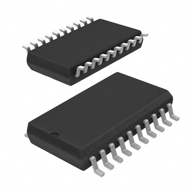
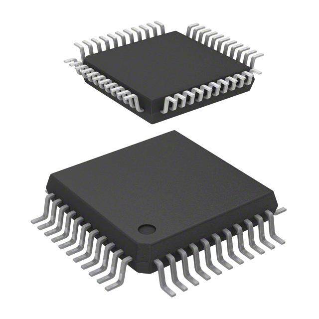
| 描述 | IC MCU 8BIT 2KB FLASH 20SOIC8位微控制器 -MCU AVR 2KB FLSH 128B EE 128B SRAM-20MHz, IND |
| EEPROM容量 | 128 x 8 |
| 产品分类 | |
| I/O数 | 16 |
| 品牌 | Atmel |
| 产品手册 | |
| 产品图片 |
|
| rohs | 符合RoHS无铅 / 符合限制有害物质指令(RoHS)规范要求 |
| 产品系列 | 嵌入式处理器和控制器,微控制器 - MCU,8位微控制器 -MCU,Atmel ATTINY261A-SURAVR® ATtiny |
| 数据手册 | |
| 产品型号 | ATTINY261A-SUR |
| RAM容量 | 128 x 8 |
| 产品培训模块 | http://www.digikey.cn/PTM/IndividualPTM.page?site=cn&lang=zhs&ptm=24997http://www.digikey.cn/PTM/IndividualPTM.page?site=cn&lang=zhs&ptm=25784http://www.digikey.cn/PTM/IndividualPTM.page?site=cn&lang=zhs&ptm=26162http://www.digikey.cn/PTM/IndividualPTM.page?site=cn&lang=zhs&ptm=26159http://www.digikey.cn/PTM/IndividualPTM.page?site=cn&lang=zhs&ptm=26180 |
| 产品种类 | 8位微控制器 -MCU |
| 供应商器件封装 | 20-SOIC |
| 其它名称 | ATTINY261A-SURCT |
| 包装 | 剪切带 (CT) |
| 可用A/D通道 | 11 |
| 商标 | Atmel |
| 商标名 | ATTINY |
| 处理器系列 | tinyAVR |
| 外设 | 欠压检测/复位,POR,PWM,温度传感器,WDT |
| 安装风格 | SMD/SMT |
| 定时器数量 | 2 |
| 封装 | Reel |
| 封装/外壳 | 20-SOIC(0.295",7.50mm 宽) |
| 封装/箱体 | SOIC-20 |
| 工作温度 | -40°C ~ 85°C |
| 工作电源电压 | 1.8 V to 5.5 V |
| 工厂包装数量 | 1000 |
| 振荡器类型 | 内部 |
| 接口类型 | Serial |
| 数据RAM大小 | 128 B |
| 数据Ram类型 | SRAM |
| 数据ROM大小 | 128 B |
| 数据Rom类型 | EEPROM |
| 数据总线宽度 | 8 bit |
| 数据转换器 | A/D 11x10b |
| 最大工作温度 | + 85 C |
| 最大时钟频率 | 20 MHz |
| 最小工作温度 | - 40 C |
| 标准包装 | 1 |
| 核心 | AVR |
| 核心处理器 | AVR |
| 核心尺寸 | 8-位 |
| 片上ADC | Yes |
| 片上DAC | Yes |
| 电压-电源(Vcc/Vdd) | 1.8 V ~ 5.5 V |
| 电源电压-最大 | 5.5 V |
| 电源电压-最小 | 1.8 V |
| 程序存储器大小 | 2 kB |
| 程序存储器类型 | Flash |
| 程序存储容量 | 2KB(1K x 16) |
| 系列 | ATTINY 261A |
| 输入/输出端数量 | 16 |
| 连接性 | USI |
| 速度 | 20MHz |


- 商务部:美国ITC正式对集成电路等产品启动337调查
- 曝三星4nm工艺存在良率问题 高通将骁龙8 Gen1或转产台积电
- 太阳诱电将投资9.5亿元在常州建新厂生产MLCC 预计2023年完工
- 英特尔发布欧洲新工厂建设计划 深化IDM 2.0 战略
- 台积电先进制程称霸业界 有大客户加持明年业绩稳了
- 达到5530亿美元!SIA预计今年全球半导体销售额将创下新高
- 英特尔拟将自动驾驶子公司Mobileye上市 估值或超500亿美元
- 三星加码芯片和SET,合并消费电子和移动部门,撤换高东真等 CEO
- 三星电子宣布重大人事变动 还合并消费电子和移动部门
- 海关总署:前11个月进口集成电路产品价值2.52万亿元 增长14.8%


PDF Datasheet 数据手册内容提取
Features • High Performance, Low Power AVR® 8-Bit Microcontroller (cid:129) Advanced RISC Architecture – 123 Powerful Instructions – Most Single Clock Cycle Execution – 32 x 8 General Purpose Working Registers – Fully Static Operation – Up to 20 MIPS Throughput at 20 MHz (cid:129) High Endurance Non-volatile Memory Segments – 2/4/8K Bytes of In-System Self-Programmable Flash Program Memory 8-bit (cid:129) Endurance: 10,000 Write/Erase Cycles – 128/256/512 Bytes of In-System Programmable EEPROM Microcontroller (cid:129) Endurance: 100,000 Write/Erase Cycles – 128/256/512 Bytes of Internal SRAM with 2/4/8K – Data retention: 20 Years at 85°C / 100 Years at 25°C – In-System Programmable via SPI Port Bytes In-System – Programming Lock for Software Security (cid:129) Peripheral Features Programmable – One 8/16-bit Timer/Counter with Prescaler Flash – One 8/10-bit High Speed Timer/Counter with Prescaler (cid:129) 3 High Frequency PWM Outputs with Separate Output Compare Registers (cid:129) Programmable Dead Time Generator – 10-bit ADC ATtiny261A (cid:129) 11 Single-Ended Channels (cid:129) 16 Differential ADC Channel Pairs ATtiny461A (cid:129) 15 Differential ADC Channel Pairs with Programmable Gain (1x, 8x, 20x, 32x) ATtiny861A – On-Chip Analog Comparator – Programmable Watchdog Timer with Separate On-Chip Oscillator – Universal Serial Interface with Start Condition Detector – Interrupt and Wake-up on Pin Change (cid:129) Special Microcontroller Features – debugWIRE On-Chip Debug System – Power-on Reset and Programmable Brown-out Detection – Internal Calibrated Oscillator – External and Internal Interrupt Sources – Four Sleep Modes: Low Power Idle, ADC Noise Reduction, Standby and Power- Down – On-Chip Temperature Sensor (cid:129) I/O and Packages – 16 Programmable I/O Lines – 20-pin PDIP, 20-pin SOIC, 20-pin TSSOP and 32-pad MLF (cid:129) Operating Voltage – 1.8 – 5.5V (cid:129) Speed Grades – 0 – 4 MHz @ 1.8 – 5.5V – 0 – 10 MHz @ 2.7 – 5.5V – 0 – 20 MHz @ 4.5 – 5.5V (cid:129) Power Consumption at 1 MHz, 1.8V, 25°C – Active: 200 µA – Power-Down Mode: 0.1 µA 8197C–AVR–05/11
1. Pin Configurations Figure 1-1. Pinout ATtiny261A/461A/861A PDIP/SOIC/TSSOP (MOSI/DI/SDA/OC1A/PCINT8) PB0 1 20 PA0 (ADC0/DI/SDA/PCINT0) (MISO/DO/OC1A/PCINT9) PB1 2 19 PA1 (ADC1/DO/PCINT1) (SCK/USCK/SCL/OC1B/PCINT10) PB2 3 18 PA2 (ADC2/INT1/USCK/SCL/PCINT2) (OC1B/PCINT11) PB3 4 17 PA3 (AREF/PCINT3) VCC 5 16 AGND GND 6 15 AVCC (ADC7/OC1D/CLKI/XTAL1/PCINT12) PB4 7 14 PA4 (ADC3/ICP0/PCINT4) (ADC8/OC1D/CLKO/XTAL2/PCINT13) PB5 8 13 PA5 (ADC4/AIN2/PCINT5) (ADC9/INT0/T0/PCINT14) PB6 9 12 PA6 (ADC5/AIN0/PCINT6) (ADC10/RESET/PCINT15) PB7 10 11 PA7 (ADC6/AIN1/PCINT7) 0) T1 8) N T CL/OC1B/PCI C1A/PCINT9) A/OC1A/PCIN A/PCINT0) CINT1) SCK/S DO/O DI/SD DI/SD DO/P SCK/U MISO/ MOSI/ ADC0/ ADC1/ B2 ( B1 ( B0 ( C C C A0 ( A1 ( P P P N N N P P 2 1 0 9 8 7 6 5 3 3 3 2 2 2 2 2 NC 1 24 NC (OC1B/PCINT11) PB3 2 23 PA2 (ADC2/INT1/USCK/SCL/PCINT2) NC 3 22 PA3 (AREF/PCINT3) VCC 4 21 AGND QFN/MLF GND 5 20 NC NC 6 19 NC (ADC7/OC1D/CLKI/XTAL1/PCINT12) PB4 7 18 AVCC (ADC8/OC1D/CLKO/XTAL2/PCINT13) PB5 8 17 PA4 (ADC3/ICP0/PCINT4) 0 1 2 3 4 5 6 9 1 1 1 1 1 1 1 C 6 7 C 7 6 5 C N B B N A A A N P P P P P 4) 5) 7) 6) 5) 1 1 T T T T T N N N CIN CIN PCI PCI PCI 0/P T/P N1/ N0/ N2/ DC9/INT0/T DC10/RESE (ADC6/AI (ADC5/AI (ADC4/AI A A ( ( Note: To ensure mechanical stability the center pad underneath the QFN/MLF package should be soldered to ground on the board. ATtiny261A/461A/861A 2 8197C–AVR–05/11
ATtiny261A/461A/861A 1.1 Pin Descriptions 1.1.1 VCC Supply voltage. 1.1.2 GND Ground. 1.1.3 AVCC Analog supply voltage. This is the supply voltage pin for the Analog-to-digital Converter (ADC), the analog comparator, the Brown-Out Detector (BOD), the internal voltage reference and Port A. It should be externally connected to VCC, even if some peripherals such as the ADC are not used. If the ADC is used AVCC should be connected to VCC through a low-pass filter. 1.1.4 AGND Analog ground. 1.1.5 Port A (PA7:PA0) An 8-bit, bi-directional I/O port with internal pull-up resistors, individually selectable for each bit. Output buffers have symmetrical drive characteristics with both high sink and source capability. As inputs, port pins that are externally pulled low will source current if pull-up resistors have been activated. Port pins are tri-stated when a reset condition becomes active, even if the clock is not running. Port A also serves the functions of various special features of the device, as listed on page 62. 1.1.6 Port B (PB7:PB0) An 8-bit, bi-directional I/O port with internal pull-up resistors, individually selectable for each bit. Output buffers have symmetrical drive characteristics with both high sink and source capability. As inputs, port pins that are externally pulled low will source current if pull-up resistors have been activated. Port pins are tri-stated when a reset condition becomes active, even if the clock is not running. Port B also serves the functions of various special features of the device, as listed on page 65. 1.1.7 RESET Reset input. A low level on this pin for longer than the minimum pulse length will generate a reset, even if the clock is not running and provided the reset pin has not been disabled. The min- imum pulse length is given in Table 19-4 on page 188. Shorter pulses are not guaranteed to generate a reset. The reset pin can also be used as a (weak) I/O pin. 3 8197C–AVR–05/11
2. Overview ATtiny261A/461A/861A are low-power CMOS 8-bit microcontrollers based on the AVR enhanced RISC architecture. By executing powerful instructions in a single clock cycle, the devices achieve throughputs approaching 1 MIPS per MHz allowing the system designer to opti- mize power consumption versus processing speed. 2.1 Block Diagram Figure 2-1. Block Diagram D C N C G V Watchdog Power debugWIRE Timer Supervision POR / BOD & Watchdog PROGRAM Oscillator RESET LOGIC Oscillator Flash SRAM Circuits / Clock Generation CPU EEPROM AVCC AGND AREF Timer/Counter0 Timer/Counter1 A/D Conv. US B A AT D Internal USI Analog Comp. Bandgap 3 11 PORT B (8) PORT A (8) RESET XTAL[1:2] PB[0:7] PA[0:7] The AVR core combines a rich instruction set with 32 general purpose working registers. All 32 registers are directly connected to the Arithmetic Logic Unit (ALU), allowing two independent registers to be accessed in one single instruction executed in one clock cycle. The resulting architecture is more code efficient while achieving throughputs up to ten times faster than con- ventional CISC microcontrollers. ATtiny261A/461A/861A 4 8197C–AVR–05/11
ATtiny261A/461A/861A The ATtiny261A/461A/861A provides the following features: 2/4/8K byte of In-System Program- mable Flash, 128/256/512 bytes EEPROM, 128/256/512 bytes SRAM, 16 general purpose I/O lines, 32 general purpose working registers, an 8-bit Timer/Counter with compare modes, an 8- bit high speed Timer/Counter, a Universal Serial Interface, Internal and External Interrupts, an 11-channel, 10-bit ADC, a programmable Watchdog Timer with internal oscillator, and four soft- ware selectable power saving modes. Idle mode stops the CPU while allowing the SRAM, Timer/Counter, ADC, Analog Comparator, and Interrupt system to continue functioning. Power- down mode saves the register contents, disabling all chip functions until the next Interrupt or Hardware Reset. ADC Noise Reduction mode stops the CPU and all I/O modules except ADC, to minimize switching noise during ADC conversions. In Standby mode, the crystal/resonator oscillator is running while the rest of the device is sleeping, allowing very fast start-up combined with low power consumption. The device is manufactured using Atmel’s high density non-volatile memory technology. The On-chip ISP Flash allows the Program memory to be re-programmed In-System through an SPI serial interface, by a conventional non-volatile memory programmer or by an On-chip boot code running on the AVR core. The ATtiny261A/461A/861A AVR is supported by a full suite of program and system develop- ment tools including: C Compilers, Macro Assemblers, Program Debugger/Simulators, and Evaluation kits. 5 8197C–AVR–05/11
3. General Information 3.1 Resources A comprehensive set of drivers, application notes, data sheets and descriptions on development tools are available for download at http://www.atmel.com/avr. 3.2 Code Examples This documentation contains simple code examples that briefly show how to use various parts of the device. These code examples assume that the part specific header file is included before compilation. Be aware that not all C compiler vendors include bit definitions in the header files and interrupt handling in C is compiler dependent. Please confirm with the C compiler documen- tation for more details. For I/O Registers located in the extended I/O map, “IN”, “OUT”, “SBIS”, “SBIC”, “CBI”, and “SBI” instructions must be replaced with instructions that allow access to extended I/O. Typically, this means “LDS” and “STS” combined with “SBRS”, “SBRC”, “SBR”, and “CBR”. Note that not all AVR devices include an extended I/O map. 3.3 Capacitive Touch Sensing Atmel QTouch Library provides a simple to use solution for touch sensitive interfaces on Atmel AVR microcontrollers. The QTouch Library includes support for QTouch® and QMatrix® acquisi- tion methods. Touch sensing is easily added to any application by linking the QTouch Library and using the Application Programming Interface (API) of the library to define the touch channels and sensors. The application then calls the API to retrieve channel information and determine the state of the touch sensor. The QTouch Library is free and can be downloaded from the Atmel website. For more informa- tion and details of implementation, refer to the QTouch Library User Guide – also available from the Atmel website. 3.4 Data Retention Reliability Qualification results show that the projected data retention failure rate is much less than 1 PPM over 20 years at 85°C or 100 years at 25°C. ATtiny261A/461A/861A 6 8197C–AVR–05/11
ATtiny261A/461A/861A 4. CPU Core This section discusses the AVR core architecture in general. The main function of the CPU core is to ensure correct program execution. The CPU must therefore be able to access memories, perform calculations, control peripherals, and handle interrupts. 4.1 Architectural Overview Figure 4-1. Block Diagram of the AVR Architecture Data Bus 8-bit Program Status Flash Counter and Control Program Memory 32 x 8 Instruction General Register Purpose Interrupt Registrers Unit Instruction Watchdog Decoder Timer g g n n si ssi es ALU Analog e r Control Lines dr dd Comparator d A ct A ect e r r di Di n I/O Module1 I Data I/O Module 2 SRAM I/O Module n EEPROM I/O Lines In order to maximize performance and parallelism, the AVR uses a Harvard architecture – with separate memories and buses for program and data. Instructions in the Program memory are executed with a single level pipelining. While one instruction is being executed, the next instruc- tion is pre-fetched from the Program memory. This concept enables instructions to be executed in every clock cycle. The Program memory is In-System Reprogrammable Flash memory. 7 8197C–AVR–05/11
The fast-access Register File contains 32 x 8-bit general purpose working registers with a single clock cycle access time. This allows single-cycle Arithmetic Logic Unit (ALU) operation. In a typ- ical ALU operation, two operands are output from the Register File, the operation is executed, and the result is stored back in the Register File – in one clock cycle. Six of the 32 registers can be used as three 16-bit indirect address register pointers for Data Space addressing – enabling efficient address calculations. One of the these address pointers can also be used as an address pointer for look up tables in Flash Program memory. These added function registers are the 16-bit X-, Y-, and Z-register, described later in this section. The ALU supports arithmetic and logic operations between registers or between a constant and a register. Single register operations can also be executed in the ALU. After an arithmetic opera- tion, the Status Register is updated to reflect information about the result of the operation. Program flow is provided by conditional and unconditional jump and call instructions, able to directly address the whole address space. Most AVR instructions have a single 16-bit word for- mat. Every Program memory address contains a 16- or 32-bit instruction. During interrupts and subroutine calls, the return address Program Counter (PC) is stored on the Stack. The Stack is effectively allocated in the general data SRAM, and consequently the Stack size is only limited by the total SRAM size and the usage of the SRAM. All user programs must initialize the SP in the Reset routine (before subroutines or interrupts are executed). The Stack Pointer (SP) is read/write accessible in the I/O space. The data SRAM can easily be accessed through the five different addressing modes supported in the AVR architecture. The memory spaces in the AVR architecture are all linear and regular memory maps. A flexible interrupt module has its control registers in the I/O space with an additional Global Interrupt Enable bit in the Status Register. All interrupts have a separate Interrupt Vector in the Interrupt Vector table. The interrupts have priority in accordance with their Interrupt Vector posi- tion. The lower the Interrupt Vector address, the higher the priority. The I/O memory space contains 64 addresses for CPU peripheral functions as Control Regis- ters, SPI, and other I/O functions. The I/O memory can be accessed directly, or as the Data Space locations following those of the Register File, 0x20 - 0x5F. 4.2 ALU – Arithmetic Logic Unit The high-performance AVR ALU operates in direct connection with all the 32 general purpose working registers. Within a single clock cycle, arithmetic operations between general purpose registers or between a register and an immediate are executed. The ALU operations are divided into three main categories – arithmetic, logical, and bit-functions. Some implementations of the architecture also provide a powerful multiplier supporting both signed/unsigned multiplication and fractional format. See the “Instruction Set” section for a detailed description. 4.3 Status Register The Status Register contains information about the result of the most recently executed arithme- tic instruction. This information can be used for altering program flow in order to perform conditional operations. Note that the Status Register is updated after all ALU operations, as specified in the Instruction Set Reference. This will in many cases remove the need for using the dedicated compare instructions, resulting in faster and more compact code. The Status Register is neither automatically stored when entering an interrupt routine, nor restored when returning from an interrupt. This must be handled by software. ATtiny261A/461A/861A 8 8197C–AVR–05/11
ATtiny261A/461A/861A 4.3.1 SREG – AVR Status Register Bit 7 6 5 4 3 2 1 0 0x3F (0x5F) I T H S V N Z C SREG Read/Write R/W R/W R/W R/W R/W R/W R/W R/W Initial Value 0 0 0 0 0 0 0 0 (cid:129) Bit 7 – I: Global Interrupt Enable The Global Interrupt Enable bit must be set for the interrupts to be enabled. The individual inter- rupt enable control is then performed in separate control registers. If the Global Interrupt Enable Register is cleared, none of the interrupts are enabled independent of the individual interrupt enable settings. The I-bit is cleared by hardware after an interrupt has occurred, and is set by the RETI instruction to enable subsequent interrupts. The I-bit can also be set and cleared by the application with the SEI and CLI instructions, as described in the instruction set reference. (cid:129) Bit 6 – T: Bit Copy Storage The Bit Copy instructions BLD (Bit LoaD) and BST (Bit STore) use the T-bit as source or desti- nation for the operated bit. A bit from a register in the Register File can be copied into T by the BST instruction, and a bit in T can be copied into a bit in a register in the Register File by the BLD instruction. (cid:129) Bit 5 – H: Half Carry Flag The Half Carry Flag H indicates a Half Carry in some arithmetic operations. Half Carry is useful in BCD arithmetic. See the “Instruction Set Description” for detailed information. (cid:129) Bit 4 – S: Sign Bit, S = N ⊕ V The S-bit is always an exclusive or between the Negative Flag N and the Two’s Complement Overflow Flag V. See the “Instruction Set Description” for detailed information. (cid:129) Bit 3 – V: Two’s Complement Overflow Flag The Two’s Complement Overflow Flag V supports two’s complement arithmetics. See the “Instruction Set Description” for detailed information. (cid:129) Bit 2 – N: Negative Flag The Negative Flag N indicates a negative result in an arithmetic or logic operation. See the “Instruction Set Description” for detailed information. (cid:129) Bit 1 – Z: Zero Flag The Zero Flag Z indicates a zero result in an arithmetic or logic operation. See the “Instruction Set Description” for detailed information. (cid:129) Bit 0 – C: Carry Flag The Carry Flag C indicates a carry in an arithmetic or logic operation. See the “Instruction Set Description” for detailed information. 9 8197C–AVR–05/11
4.4 General Purpose Register File The Register File is optimized for the AVR Enhanced RISC instruction set. In order to achieve the required performance and flexibility, the following input/output schemes are supported by the Register File: (cid:129) One 8-bit output operand and one 8-bit result input (cid:129) Two 8-bit output operands and one 8-bit result input (cid:129) Two 8-bit output operands and one 16-bit result input (cid:129) One 16-bit output operand and one 16-bit result input Figure 4-2 below shows the structure of the 32 general purpose working registers in the CPU. Figure 4-2. AVR CPU General Purpose Working Registers 7 0 Addr. R0 0x00 R1 0x01 R2 0x02 … R13 0x0D General R14 0x0E Purpose R15 0x0F Working R16 0x10 Registers R17 0x11 … R26 0x1A X-register Low Byte R27 0x1B X-register High Byte R28 0x1C Y-register Low Byte R29 0x1D Y-register High Byte R30 0x1E Z-register Low Byte R31 0x1F Z-register High Byte Most of the instructions operating on the Register File have direct access to all registers, and most of them are single cycle instructions. As shown in Figure 4-2, each register is also assigned a Data memory address, mapping them directly into the first 32 locations of the user Data Space. Although not being physically imple- mented as SRAM locations, this memory organization provides great flexibility in access of the registers, as the X-, Y- and Z-pointer registers can be set to index any register in the file. 4.4.1 The X-register, Y-register, and Z-register The registers R26:R31 have some added functions to their general purpose usage. These regis- ters are 16-bit address pointers for indirect addressing of the data space. The three indirect address registers X, Y, and Z are defined as described in Figure 4-3. Figure 4-3. The X-, Y-, and Z-registers 15 XH XL 0 X-register 7 0 7 0 R27 (0x1B) R26 (0x1A) ATtiny261A/461A/861A 10 8197C–AVR–05/11
ATtiny261A/461A/861A 15 YH YL 0 Y-register 7 0 7 0 R29 (0x1D) R28 (0x1C) 15 ZH ZL 0 Z-register 7 0 7 0 R31 (0x1F) R30 (0x1E) In different addressing modes these address registers function as automatic increment and automatic decrement (see the instruction set reference for details). 4.5 Stack Pointer The Stack is mainly used for storing temporary data, local variables and return addresses for interrupts and subroutine calls. The Stack Pointer Register always points to the top of the Stack, in the data SRAM Stack area where the subroutine and interrupt stacks are located. The Stack in the data SRAM must be defined by the program before any subroutine calls are executed or interrupts are enabled. The Stack Pointer must be set to point above start of the SRAM (see Figure 5-2 on page 16). The initial Stack Pointer value equals the last address of the internal SRAM. Note that the Stack is implemented as growing from higher to lower memory locations. This means a Stack PUSH command decreases the Stack Pointer. See Table 4-1. Table 4-1. Stack Pointer instructions Instruction Stack pointer Description PUSH Decremented by 1 Data is pushed onto the stack ICALL Return address is pushed onto the stack with a Decremented by 2 RCALL subroutine call or interrupt POP Incremented by 1 Data is popped from the stack RET Return address is popped from the stack with return Incremented by 2 RETI from subroutine or return from interrupt The AVR Stack Pointer is implemented as two 8-bit registers in the I/O space. The number of bits actually used is implementation dependent. Note that the data space in some implementations of the AVR architecture is so small that only SPL is needed. In this case, the SPH Register will not be present. 4.5.1 SPH and SPL – Stack Pointer Register Bit 15 14 13 12 11 10 9 8 0x3E (0x5E) SP15 SP14 SP13 SP12 SP11 SP10 SP9 SP8 SPH 0x3D (0x5D) SP7 SP6 SP5 SP4 SP3 SP2 SP1 SP0 SPL 7 6 5 4 3 2 1 0 Read/Write R/W R/W R/W R/W R/W R/W R/W R/W R/W R/W R/W R/W R/W R/W R/W R/W Initial Value RAMEND RAMEND RAMEND RAMEND RAMEND RAMEND RAMEND RAMEND RAMEND RAMEND RAMEND RAMEND RAMEND RAMEND RAMEND RAMEND 11 8197C–AVR–05/11
4.6 Instruction Execution Timing This section describes the general access timing concepts for instruction execution. The AVR CPU is driven by the CPU clock clk , directly generated from the selected clock source for the CPU chip. No internal clock division is used. Figure 4-4 shows the parallel instruction fetches and instruction executions enabled by the Har- vard architecture and the fast access Register File concept. This is the basic pipelining concept to obtain up to 1 MIPS per MHz with the corresponding unique results for functions per cost, functions per clocks, and functions per power-unit. Figure 4-4. The Parallel Instruction Fetches and Instruction Executions T1 T2 T3 T4 clk CPU 1st Instruction Fetch 1st Instruction Execute 2nd Instruction Fetch 2nd Instruction Execute 3rd Instruction Fetch 3rd Instruction Execute 4th Instruction Fetch Figure 4-5 shows the internal timing concept for the Register File. In a single clock cycle an ALU operation using two register operands is executed, and the result is stored back to the destina- tion register. Figure 4-5. Single Cycle ALU Operation T1 T2 T3 T4 clk CPU Total Execution Time Register Operands Fetch ALU Operation Execute Result Write Back 4.7 Reset and Interrupt Handling The AVR provides several different interrupt sources. These interrupts and the separate Reset Vector each have a separate Program Vector in the Program memory space. All interrupts are assigned individual enable bits which must be written logic one together with the Global Interrupt Enable bit in the Status Register in order to enable the interrupt. The lowest addresses in the Program memory space are by default defined as the Reset and Interrupt Vectors. The complete list of vectors is shown in “Interrupts” on page 49. The list also determines the priority levels of the different interrupts. The lower the address the higher is the ATtiny261A/461A/861A 12 8197C–AVR–05/11
ATtiny261A/461A/861A priority level. RESET has the highest priority, and next is INT0 – the External Interrupt Request0. When an interrupt occurs, the Global Interrupt Enable I-bit is cleared and all interrupts are dis- abled. The user software can write logic one to the I-bit to enable nested interrupts. All enabled interrupts can then interrupt the current interrupt routine. The I-bit is automatically set when a Return from Interrupt instruction – RETI – is executed. There are basically two types of interrupts. The first type is triggered by an event that sets the Interrupt Flag. For these interrupts, the Program Counter is vectored to the actual Interrupt Vec- tor in order to execute the interrupt handling routine, and hardware clears the corresponding Interrupt Flag. Interrupt Flags can also be cleared by writing a logic one to the flag bit position(s) to be cleared. If an interrupt condition occurs while the corresponding interrupt enable bit is cleared, the Interrupt Flag will be set and remembered until the interrupt is enabled, or the flag is cleared by software. Similarly, if one or more interrupt conditions occur while the Global Interrupt Enable bit is cleared, the corresponding Interrupt Flag(s) will be set and remembered until the Global Interrupt Enable bit is set, and will then be executed by order of priority. The second type of interrupts will trigger as long as the interrupt condition is present. These interrupts do not necessarily have Interrupt Flags. If the interrupt condition disappears before the interrupt is enabled, the interrupt will not be triggered. When the AVR exits from an interrupt, it will always return to the main program and execute one more instruction before any pending interrupt is served. Note that the Status Register is not automatically stored when entering an interrupt routine, nor restored when returning from an interrupt routine. This must be handled by software. When using the CLI instruction to disable interrupts, the interrupts will be immediately disabled. No interrupt will be executed after the CLI instruction, even if it occurs simultaneously with the CLI instruction. The following example shows how this can be used to avoid interrupts during the timed EEPROM write sequence. Assembly Code Example in r16, SREG ; store SREG value cli ; disable interrupts during timed sequence sbiEECR, EEMPE ; start EEPROM write sbiEECR, EEPE outSREG, r16 ; restore SREG value (I-bit) C Code Example char cSREG; cSREG = SREG;/* store SREG value */ /* disable interrupts during timed sequence */ _CLI(); EECR |= (1<<EEMPE); /* start EEPROM write */ EECR |= (1<<EEPE); SREG = cSREG; /* restore SREG value (I-bit) */ Note: See “Code Examples” on page 6. 13 8197C–AVR–05/11
When using the SEI instruction to enable interrupts, the instruction following SEI will be exe- cuted before any pending interrupts, as shown in the following examples. Assembly Code Example sei ; set Global Interrupt Enable sleep ; enter sleep, waiting for interrupt ; note: will enter sleep before any pending interrupt(s) C Code Example _SEI(); /* set Global Interrupt Enable */ _SLEEP(); /* enter sleep, waiting for interrupt */ /* note: will enter sleep before any pending interrupt(s) */ Note: See “Code Examples” on page 6. 4.7.1 Interrupt Response Time The interrupt execution response for all the enabled AVR interrupts is four clock cycles mini- mum. After four clock cycles the Program Vector address for the actual interrupt handling routine is executed. During this four clock cycle period, the Program Counter is pushed onto the Stack. The vector is normally a jump to the interrupt routine, and this jump takes three clock cycles. If an interrupt occurs during execution of a multi-cycle instruction, this instruction is completed before the interrupt is served. If an interrupt occurs when the MCU is in sleep mode, the interrupt execution response time is increased by four clock cycles. This increase comes in addition to the start-up time from the selected sleep mode. A return from an interrupt handling routine takes four clock cycles. During these four clock cycles, the Program Counter (two bytes) is popped back from the Stack, the Stack Pointer is incremented by two, and the I-bit in SREG is set. ATtiny261A/461A/861A 14 8197C–AVR–05/11
ATtiny261A/461A/861A 5. Memories This section describes the different memories of the ATtiny261A/461A/861A. The AVR architec- ture has two main memory spaces, the Data memory and the Program memory space. In addition, the ATtiny261A/461A/861A features an EEPROM Memory for data storage. All three memory spaces are linear and regular. 5.1 In-System Re-programmable Flash Program Memory The ATtiny261A/461A/861A contains 2/4/8K byte On-chip In-System Reprogrammable Flash memory for program storage. Since all AVR instructions are 16 or 32 bits wide, the Flash is orga- nized as 1024/2048/4096 x 16. The Flash memory has an endurance of at least 10,000 write/erase cycles. The ATtiny261A/461A/861A Program Counter (PC) is 10/11/12 bits wide, thus capable of addressing the 1024/2048/4096 Program memory locations. “Memory Programming” on page 168 contains a detailed description on Flash data serial downloading using the SPI pins. Constant tables can be allocated within the entire address space of program memory (see the LPM – Load Program memory instruction description). Timing diagrams for instruction fetch and execution are presented in “Instruction Execution Tim- ing” on page 12. Figure 5-1. Program Memory Map Program Memory 0x0000 0x03FF/0x07FF/0x0FFF 5.2 SRAM Data Memory Figure 5-2 on page 16 shows how the ATtiny261A/461A/861A SRAM Memory is organized. The lower data memory locations address both the Register File, the I/O memory and the inter- nal data SRAM. The first 32 locations address the Register File, the next 64 locations the standard I/O memory, and the last 128/256/512 locations address the internal data SRAM. The five different addressing modes for the Data memory cover: Direct, Indirect with Displace- ment, Indirect, Indirect with Pre-decrement, and Indirect with Post-increment. In the Register File, registers R26 to R31 feature the indirect addressing pointer registers. The direct addressing reaches the entire data space. The Indirect with Displacement mode reaches 63 address locations from the base address given by the Y- or Z-register. 15 8197C–AVR–05/11
When using register indirect addressing modes with automatic pre-decrement and post-incre- ment, the address registers X, Y, and Z are decremented or incremented. The 32 general purpose working registers, 64 I/O Registers, and the 128/256/512 bytes of inter- nal data SRAM in the ATtiny261A/461A/861A are all accessible through all these addressing modes. The Register File is described in “General Purpose Register File” on page 10. Figure 5-2. Data Memory Map Data Memory 32 Registers 0x0000 - 0x001F 64 I/O Registers 0x0020 - 0x005F 0x0060 Internal SRAM (128/256/512 x 8) 0x0DF/0x15F/0x25F 5.2.1 Data Memory Access Times This section describes the general access timing concepts for internal memory access. The internal data SRAM access is performed in two clk cycles as illustrated in Figure 5-3. CPU Figure 5-3. On-chip Data SRAM Access Cycles T1 T2 T3 clk CPU Address Compute Address Address valid Data e Writ WR Data d a e R RD Memory Access Instruction Next Instruction 5.3 EEPROM Data Memory The ATtiny261A/461A/861A contains 128/256/512 bytes of data EEPROM memory. It is orga- nized as a separate data space, in which single bytes can be read and written. The EEPROM has an endurance of at least 100,000 write/erase cycles. The access between the EEPROM and the CPU is described in the following, specifying the EEPROM Address Registers, the EEPROM Data Register, and the EEPROM Control Register. For a detailed description of Serial data downloading to the EEPROM, see “Electrical Characteristics” on page 185. ATtiny261A/461A/861A 16 8197C–AVR–05/11
ATtiny261A/461A/861A 5.3.1 EEPROM Read/Write Access The EEPROM Access Registers are accessible in the I/O space. The write access times for the EEPROM are given in Table 5-1 on page 22. A self-timing func- tion, however, lets the user software detect when the next byte can be written. If the user code contains instructions that write the EEPROM, some precautions must be taken. In heavily fil- tered power supplies, V is likely to rise or fall slowly on Power-up/down. This causes the CC device for some period of time to run at a voltage lower than specified as minimum for the clock frequency used. See “Preventing EEPROM Corruption” on page 19 for details on how to avoid problems in these situations. In order to prevent unintentional EEPROM writes, a specific write procedure must be followed. Refer to “Atomic Byte Programming” on page 17 and “Split Byte Programming” on page 17 for details on this. When the EEPROM is read, the CPU is halted for four clock cycles before the next instruction is executed. When the EEPROM is written, the CPU is halted for two clock cycles before the next instruction is executed. 5.3.2 Atomic Byte Programming Using Atomic Byte Programming is the simplest mode. When writing a byte to the EEPROM, the user must write the address into the EEARL Register and data into EEDR Register. If the EEPMn bits are zero, writing EEPE (within four cycles after EEMPE is written) will trigger the erase/write operation. Both the erase and write cycle are done in one operation and the total programming time is given in Table 5-1 on page 22. The EEPE bit remains set until the erase and write operations are completed. While the device is busy with programming, it is not possi- ble to do any other EEPROM operations. 5.3.3 Split Byte Programming It is possible to split the erase and write cycle in two different operations. This may be useful if the system requires short access time for some limited period of time (typically if the power sup- ply voltage falls). In order to take advantage of this method, it is required that the locations to be written have been erased before the write operation. But since the erase and write operations are split, it is possible to do the erase operations when the system allows doing time-critical operations (typically after Power-up). 5.3.4 Erase To erase a byte, the address must be written to EEAR. If the EEPMn bits are 0b01, writing the EEPE within four cycles after EEMPE is written will trigger the erase operation only (program- ming time is given in Table 5-1 on page 22). The EEPE bit remains set until the erase operation completes. While the device is busy programming, it is not possible to do any other EEPROM operations. 5.3.5 Write To write a location, the user must write the address into EEAR and the data into EEDR. If the EEPMn bits are 0b10, writing the EEPE (within four cycles after EEMPE is written) will trigger the write operation only (programming time is given in Table 5-1 on page 22). The EEPE bit remains set until the write operation completes. If the location to be written has not been erased before write, the data that is stored must be considered as lost. While the device is busy with programming, it is not possible to do any other EEPROM operations. 17 8197C–AVR–05/11
The calibrated Oscillator is used to time the EEPROM accesses. Make sure the Oscillator fre- quency is within the requirements described in “OSCCAL – Oscillator Calibration Register” on page 32. 5.3.6 Program Examples The following code examples show one assembly and one C function for erase, write, or atomic write of the EEPROM. The examples assume that interrupts are controlled (e.g., by disabling interrupts globally) so that no interrupts will occur during execution of these functions. Assembly Code Example EEPROM_write: ; Wait for completion of previous write sbic EECR,EEPE rjmp EEPROM_write ; Set Programming mode ldi r16, (0<<EEPM1)|(0<<EEPM0) out EECR, r16 ; Set up address (r18:r17) in address register out EEARH, r18 out EEARL, r17 ; Write data (r19) to data register out EEDR, r19 ; Write logical one to EEMPE sbi EECR,EEMPE ; Start eeprom write by setting EEPE sbi EECR,EEPE ret C Code Example void EEPROM_write(unsigned char ucAddress, unsigned char ucData) { /* Wait for completion of previous write */ while(EECR & (1<<EEPE)) ; /* Set Programming mode */ EECR = (0<<EEPM1)|(0<<EEPM0); /* Set up address and data registers */ EEAR = ucAddress; EEDR = ucData; /* Write logical one to EEMPE */ EECR |= (1<<EEMPE); /* Start eeprom write by setting EEPE */ EECR |= (1<<EEPE); } Note: See “Code Examples” on page 6. ATtiny261A/461A/861A 18 8197C–AVR–05/11
ATtiny261A/461A/861A The next code examples show assembly and C functions for reading the EEPROM. The exam- ples assume that interrupts are controlled so that no interrupts will occur during execution of these functions. Assembly Code Example EEPROM_read: ; Wait for completion of previous write sbic EECR,EEPE rjmp EEPROM_read ; Set up address (r18:r17) in address register out EEARH, r18 out EEARL, r17 ; Start eeprom read by writing EERE sbi EECR,EERE ; Read data from data register in r16,EEDR ret C Code Example unsigned char EEPROM_read(unsigned char ucAddress) { /* Wait for completion of previous write */ while(EECR & (1<<EEPE)) ; /* Set up address register */ EEAR = ucAddress; /* Start eeprom read by writing EERE */ EECR |= (1<<EERE); /* Return data from data register */ return EEDR; } Note: See “Code Examples” on page 6. 5.3.7 Preventing EEPROM Corruption During periods of low V , the EEPROM data can be corrupted because the supply voltage is CC too low for the CPU and the EEPROM to operate properly. These issues are the same as for board level systems using EEPROM, and the same design solutions should be applied. An EEPROM data corruption can be caused by two situations when the voltage is too low. First, a regular write sequence to the EEPROM requires a minimum voltage to operate correctly. Sec- ondly, the CPU itself can execute instructions incorrectly, if the supply voltage is too low. EEPROM data corruption can easily be avoided by following this design recommendation: Keep the AVR RESET active (low) during periods of insufficient power supply voltage. This can be done by enabling the internal Brown-out Detector (BOD). If the detection level of the internal BOD does not match the needed detection level, an external low V reset protection circuit can CC 19 8197C–AVR–05/11
be used. If a reset occurs while a write operation is in progress, the write operation will be com- pleted provided that the power supply voltage is sufficient. 5.4 I/O Memory The I/O space definition of the ATtiny261A/461A/861A is shown in “Register Summary” on page 277. All I/Os and peripherals are placed in the I/O space. All I/O locations may be accessed using the LD/LDS/LDD and ST/STS/STD instructions, enabling data transfer between the 32 general pur- pose working registers and the I/O space. I/O Registers within the address range 0x00 - 0x1F are directly bit-accessible using the SBI and CBI instructions. In these registers, the value of sin- gle bits can be checked by using the SBIS and SBIC instructions. Refer to the instruction set section for more details. When using the I/O specific commands IN and OUT, the I/O addresses 0x00 - 0x3F must be used. When addressing I/O Registers as data space using LD and ST instructions, 0x20 must be added to these addresses. For compatibility with future devices, reserved bits should be written to zero if accessed. Reserved I/O memory addresses should never be written. Some of the Status Flags are cleared by writing a logical one to them. Note that, the CBI and SBI instructions will only operate on the specified bit, and can therefore be used on registers containing such Status Flags. The CBI and SBI instructions work on registers in the address range 0x00 to 0x1F, only. The I/O and Peripherals Control Registers are explained in later sections. 5.4.1 General Purpose I/O Registers The ATtiny261A/461A/861A contains three General Purpose I/O Registers. These registers can be used for storing any information, and they are particularly useful for storing global variables and Status Flags. General Purpose I/O Registers within the address range 0x00 - 0x1F are directly bit-accessible using the SBI, CBI, SBIS, and SBIC instructions. 5.5 Register Description 5.5.1 EEARH – EEPROM Address Register Bit 7 6 5 4 3 2 1 0 0x1F (0x3F) – – – – – – – EEAR8 EEARH Read/Write R R R R R R R R/W Initial Value 0 0 0 0 0 0 0 X/0 (cid:129) Bits 7:1 – Res: Reserved Bits These bits are reserved and will always read as zero. (cid:129) Bit 0 – EEAR8: EEPROM Address This is the most significant EEPROM address bit of ATtiny861A. In devices with less EEPROM, i.e. ATtiny261A/ATtiny461A, this bit is reserved and will always read zero. The initial value of the EEPROM Address Register (EEAR) is undefined and a proper value must therefore be written before the EEPROM is accessed. ATtiny261A/461A/861A 20 8197C–AVR–05/11
ATtiny261A/461A/861A 5.5.2 EEARL – EEPROM Address Register Bit 7 6 5 4 3 2 1 0 0x1E (0x3E) EEAR7 EEAR6 EEAR5 EEAR4 EEAR3 EEAR2 EEAR1 EEAR0 EEARL Read/Write R/W R/W R/W R/W R/W R/W R/W R/W Initial Value X/0 X X X X X X X (cid:129) Bit 7 – EEAR7: EEPROM Address This is the most significant EEPROM address bit of ATtiny461A. In devices with less EEPROM, i.e. ATtiny261A, this bit is reserved and will always read zero. The initial value of the EEPROM Address Register (EEAR) is undefined and a proper value must therefore be written before the EEPROM is accessed. (cid:129) Bits 6:0 – EEAR[6: 0]: EEPROM Address These are the (low) bits of the EEPROM Address Register. The EEPROM data bytes are addressed linearly in the range 0...128/256/512. The initial value of EEAR is undefined and a proper value must be therefore be written before the EEPROM may be accessed. 5.5.3 EEDR – EEPROM Data Register Bit 7 6 5 4 3 2 1 0 0x1D (0x3D) EEDR7 EEDR6 EEDR5 EEDR4 EEDR3 EEDR2 EEDR1 EEDR0 EEDR Read/Write R/W R/W R/W R/W R/W R/W R/W R/W Initial Value 0 0 0 0 0 0 0 0 (cid:129) Bits 7:0 – EEDR[7:0]: EEPROM Data For the EEPROM write operation the EEDR Register contains the data to be written to the EEPROM in the address given by the EEAR Register. For the EEPROM read operation, the EEDR contains the data read out from the EEPROM at the address given by EEAR. 5.5.4 EECR – EEPROM Control Register Bit 7 6 5 4 3 2 1 0 0x1C (0x3C) – – EEPM1 EEPM0 EERIE EEMPE EEPE EERE EECR Read/Write R R R/W R/W R/W R/W R/W R/W Initial Value 0 0 X X 0 0 X 0 (cid:129) Bit 7 – Res: Reserved Bit This bit is reserved for future use and will always read zero. For compatibility with future AVR devices, always write this bit to zero. After reading, mask out this bit. (cid:129) Bit 6 – Res: Reserved Bit This bit is reserved and will always read as zero. (cid:129) Bits 5:4 – EEPM[1:0]: EEPR OM Programming Mode Bits The EEPROM Programming mode bits setting defines which programming action that will be triggered when writing EEPE. It is possible to program data in one atomic operation (erase the 21 8197C–AVR–05/11
old value and program the new value) or to split the Erase and Write operations in two different operations. The Programming times for the different modes are shown in Table 5-1. Table 5-1. EEPROM Mode Bits Programming EEPM1 EEPM0 Time Operation 0 0 3.4 ms Erase and Write in one operation (Atomic Operation) 0 1 1.8 ms Erase Only 1 0 1.8 ms Write Only 1 1 – Reserved for future use When EEPE is set, any write to EEPMn will be ignored. During reset, the EEPMn bits will be reset to 0b00 unless the EEPROM is busy programming. (cid:129) Bit 3 – EERIE: EEPROM Ready Interrupt Enable Writing EERIE to one enables the EEPROM Ready Interrupt if the I-bit in SREG is set. Writing EERIE to zero disables the interrupt. The EEPROM Ready Interrupt generates a constant inter- rupt when Non-volatile memory is ready for programming. (cid:129) Bit 2 – EEMPE: EEPROM Master Program Enable The EEMPE bit determines whether writing EEPE to one will have effect or not. When EEMPE is set, setting EEPE within four clock cycles will program the EEPROM at the selected address. If EEMPE is zero, setting EEPE will have no effect. When EEMPE has been written to one by software, hardware clears the bit to zero after four clock cycles. (cid:129) Bit 1 – EEPE: EEPROM Program Enable The EEPROM Program Enable Signal EEPE is the programming enable signal to the EEPROM. When EEPE is written, the EEPROM will be programmed according to the EEPMn bits setting. The EEMPE bit must be written to one before a logical one is written to EEPE, otherwise no EEPROM write takes place. When the write access time has elapsed, the EEPE bit is cleared by hardware. When EEPE has been set, the CPU is halted for two cycles before the next instruction is executed. (cid:129) Bit 0 – EERE: EEPROM Read Enable The EEPROM Read Enable Signal – EERE – is the read strobe to the EEPROM. When the cor- rect address is set up in the EEAR Register, the EERE bit must be written to one to trigger the EEPROM read. The EEPROM read access takes one instruction, and the requested data is available immediately. When the EEPROM is read, the CPU is halted for four cycles before the next instruction is executed. The user should poll the EEPE bit before starting the read opera- tion. If a write operation is in progress, it is neither possible to read the EEPROM, nor to change the EEAR Register. ATtiny261A/461A/861A 22 8197C–AVR–05/11
ATtiny261A/461A/861A 5.5.5 GPIOR2 – General Purpose I/O Register 2 Bit 7 6 5 4 3 2 1 0 0x0C (0x2C) MSB LSB GPIOR2 Read/Write R/W R/W R/W R/W R/W R/W R/W R/W Initial Value 0 0 0 0 0 0 0 0 5.5.6 GPIOR1 – General Purpose I/O Register 1 Bit 7 6 5 4 3 2 1 0 0x0B (0x2B) MSB LSB GPIOR1 Read/Write R/W R/W R/W R/W R/W R/W R/W R/W Initial Value 0 0 0 0 0 0 0 0 5.5.7 GPIOR0 – General Purpose I/O Register 0 Bit 7 6 5 4 3 2 1 0 0x0A (0x2A) MSB LSB GPIOR0 Read/Write R/W R/W R/W R/W R/W R/W R/W R/W Initial Value 0 0 0 0 0 0 0 0 23 8197C–AVR–05/11
6. Clock System Figure 6-1 presents the principal clock systems and their distribution. All of the clocks need not be active at a given time. In order to reduce power consumption, the clocks to modules not being used can be halted by using different sleep modes, as described in “Power Management and Sleep Modes” on page 35. Figure 6-1. Clock Distribution General I/O General I/O Flash and ADC CPU Core RAM Modules Modules EEPROM clk ADC clkI/O AVR Clock clkCPU Control Unit clk FLASH Reset Logic Watchdog Timer Source clock Watchdog clock System Clock Prescaler Clock Watchdog Multiplexer Oscillator clk clk PCK PLL PLL Crystal LCoawl-ibFrraetqeude RncCy Calibrated RC External Clock Oscillator Oscillator CrysOtaslc Oillsactoillrator Oscillator 6.1 Clock Subsystems The clock subsystems are detailed in the sections below. 6.1.1 CPU Clock – clk CPU The CPU clock is routed to parts of the system concerned with operation of the AVR core. Examples of such modules are the General Purpose Register File, the Status Register and the Data memory holding the Stack Pointer. Halting the CPU clock inhibits the core from performing general operations and calculations. 6.1.2 I/O Clock – clk I/O The I/O clock is used by the majority of the I/O modules, like Timer/Counter. The I/O clock is also used by the External Interrupt module, but note that some external interrupts are detected by asynchronous logic, allowing such interrupts to be detected even if the I/O clock is halted. ATtiny261A/461A/861A 24 8197C–AVR–05/11
ATtiny261A/461A/861A 6.1.3 Flash Clock – clk FLASH The Flash clock controls operation of the Flash interface. The Flash clock is usually active simul- taneously with the CPU clock. 6.1.4 ADC Clock – clk ADC The ADC is provided with a dedicated clock domain. This allows halting the CPU and I/O clocks in order to reduce noise generated by digital circuitry. This gives more accurate ADC conversion results. 6.1.5 Fast Peripheral Clock – clk PCK Selected peripherals can be clocked at a frequency higher than the CPU core. The fast periph- eral clock is generated by an on-chip PLL circuit. 6.1.6 PLL System Clock – clk ADC The PLL can also be used to generate a system clock. The clock signal can be prescaled to avoid overclocking the CPU. 6.2 Clock Sources The device has the following clock source options, selectable by Flash Fuse bits as shown below. The clock from the selected source is input to the AVR clock generator, and routed to the appropriate modules. Table 6-1. Device Clocking Options Select(1) vs. PB4 and PB5 Functionality Device Clocking Option CKSEL[3:0] PB4 PB5 External Clock (see page 26) 0000 XTAL1 I/O High-Frequency PLL Clock (see page 26) 0001 I/O I/O Calibrated Internal 8 MHz Oscillator (see page 28) 0010 I/O I/O Internal 128 kHz Oscillator (see page 29) 0011 I/O I/O Low-Frequency Crystal Oscillator (see page 29) 01xx XTAL1 XTAL2 Crystal Oscillator / Ceramic Resonator 1000 XTAL1 XTAL2 0.4...0.9 MHz (see page 30) 1001 Crystal Oscillator / Ceramic Resonator 1010 XTAL1 XTAL2 0.9...3.0 MHz (see page 30) 1011 Crystal Oscillator / Ceramic Resonator 1100 XTAL1 XTAL2 3...8 MHz (see page 30) 1101 Crystal Oscillator / Ceramic Resonator 1110 XTAL1 XTAL2 8...20 MHz (see page 30) 1111 Note: 1. For all fuses “1” means unprogrammed and “0” means programmed. The various choices for each clocking option is given in the following sections. When the CPU wakes up from Power-down or Power-save, the selected clock source is used to time the start- up, ensuring stable oscillator operation before instruction execution starts. When the CPU starts from reset, there is an additional delay allowing the power to reach a stable level before com- 25 8197C–AVR–05/11
mencing normal operation. The watchdog oscillator is used for timing this real-time part of the start-up time. The number of WD oscillator cycles used for each time-out is shown in Table 6-2. Table 6-2. Number of Watchdog Oscillator Cycles Typ Time-out Number of Cycles 4 ms 512 64 ms 8K (8,192) 6.2.1 External Clock To drive the device from an external clock source, CLKI should be driven as shown in Figure 6- 2. To run the device on an external clock, the CKSEL Fuses must be programmed to “0000”. Figure 6-2. External Clock Drive Configuration EXTERNAL CLOCK CLKI SIGNAL GND When this clock source is selected, start-up times are determined by the SUT Fuses as shown in Table 6-3. Table 6-3. Start-up Times for the External Clock Selection Start-up Time from Power- Additional Delay from SUT[1:0] down and Power-save Reset Recommended Usage 00 6 CK 14CK BOD enabled 01 6 CK 14CK + 4 ms Fast rising power 10 6 CK 14CK + 64 ms Slowly rising power 11 Reserved When applying an external clock, it is required to avoid sudden changes in the applied clock fre- quency to ensure stable operation of the MCU. A variation in frequency of more than 2% from one clock cycle to the next can lead to unpredictable behavior. It is required to ensure that the MCU is kept in Reset during such changes in the clock frequency. Note that the system clock prescaler can be used to implement run-time changes of the internal clock frequency. See “System Clock Prescaler” on page 31 for details. 6.2.2 High-Frequency PLL Clock The internal PLL generates a clock signal with a frequency eight times higher than the source input. The PLL uses the output of the internal 8 MHz oscillator as source and the default setting generates a fast peripheral clock signal of 64 MHz. ATtiny261A/461A/861A 26 8197C–AVR–05/11
ATtiny261A/461A/861A The fast peripheral clock, clk , can be selected as the clock source for Timer/Counter1 and a PCK prescaled version of the PLL output, clk , can be selected as system clock. See Figure 6-3 for PLL a detailed illustration on the PLL clock system. Figure 6-3. PCK Clocking System OSCCAL LSM PLLE CKSEL3:0 CLKPS3:0 LOCK DETECTOR PLOCK 1/2 4 MHz 8 MHz clkPCK OSCILLATOR 8 MHz PLL 8x 1/4 64 / 32 MHz 16 MHz PRESCALER XTAL1 8 MHz clkPLL XTAL2 OSCILLATORS The internal PLL is enabled when CKSEL fuse bits are programmed to ‘0001’and the PLLE bit of PLLCSR is set. The internal oscillator and the PLL are switched off in power down and stand-by sleep modes. When the LSM bit of PLLCSR is set, the PLL switches from using the output of the internal 8 MHz oscillator to using the output divided by two. The frequency of the fast peripheral clock is effectively divided by two, resulting in a clock frequency of 32 MHz. The LSM bit can not be set if PLL is used as a system clock. CLK Since the PLL is locked to the output of the internal 8 MHz oscillator, adjusting the oscillator fre- quency via the OSCCAL register also changes the frequency of the fast peripheral clock. It is possible to adjust the frequency of the internal oscillator to well above 8 MHz but the fast periph- eral clock will saturate and remain oscillating at about 85 MHz. In this case the PLL is no longer locked to the internal oscillator clock signal. Therefore, in order to keep the PLL in the correct operating range, it is recommended to program the OSCCAL registers such that the oscillator frequency does not exceed 8 MHz. The PLOCK bit in PLLCSR is set when PLL is locked. Programming CKSEL fuse bits to ‘0001’, the PLL output divided by four will be used as a system clock, as shown in Table 6-4. Table 6-4. PLLCK Operating Modes CKSEL[3:0] Nominal Frequency 0001 16 MHz 27 8197C–AVR–05/11
When the PLL output is selected as clock source, the start-up times are determined by SUT fuse bits as shown in Table 6-5. Table 6-5. Start-up Times for the PLLCK Start-up Time from Additional Delay from Recommended SUT[1:0] Power Down Power-On-Reset (V = 5.0V) usage CC 00 14CK + 1K (1024) + 4 ms 4 ms BOD enabled 01 14CK + 16K (16384) + 4 ms 4 ms Fast rising power 10 14CK + 1K (1024) + 64 ms 4 ms Slowly rising power 11 14CK + 16K (16384) + 64 ms 4 ms Slowly rising power 6.2.3 Calibrated Internal 8 MHz Oscillator By default, the Internal Oscillator provides an approximately 8 MHz clock signal. Though voltage and temperature dependent, this clock can be very accurately calibrated by the user. See Table 19-2 on page 187 and “Internal Oscillators” on page 222 for more details. The device is shipped with the CKDIV8 Fuse programmed. See “System Clock Prescaler” on page 31 for more details. This clock may be selected as the system clock by programming the CKSEL Fuses as shown in Table 6-6. If selected, it will operate with no external components. During reset, hardware loads the pre-programmed calibration value into the OSCCAL Register and thereby automatically cal- ibrates the internal oscillator. The accuracy of this calibration is shown as Factory calibration in Table 19-2 on page 187. Table 6-6. Internal Calibrated Oscillator Operating Modes CKSEL[3:0] Nominal Frequency 0010 (1) 8.0 MHz (2) Notes: 1. The device is shipped with this option selected. 2. If the oscillator frequency exceeds the specification of the device (depends on V ), the CC CKDIV8 Fuse can be programmed to divide the internal frequency by 8. When this oscillator is selected, start-up times are determined by SUT fuses as shown in Table 6-7. Table 6-7. Start-up Times for the Internal Calibrated Oscillator Clock Selection Start-up Time Additional Delay from Recommended SUT[1:0] from Power-down Reset (V = 5.0V) Usage CC 00 6 CK 14CK(1) BOD enabled 01 6 CK 14CK + 4 ms Fast rising power 10(2) 6 CK 14CK + 64 ms Slowly rising power 11 Reserved Note: 1. If the RSTDISBL fuse is programmed, this start-up time will be increased to 14CK + 4 ms to ensure programming mode can be entered. 2. The device is shipped with this option selected. ATtiny261A/461A/861A 28 8197C–AVR–05/11
ATtiny261A/461A/861A It is possible to reach a higher accuracy than factory calibration by changing the OSCCAL regis- ter from software. See “OSCCAL – Oscillator Calibration Register” on page 32. The accuracy of this calibration is shown as User calibration in Table 19-2 on page 187. When this oscillator is used as device clock, the Watchdog Oscillator will still be used for the Watchdog Timer and for the Reset Time-out. For more information on the pre-programmed cali- bration value, see section “Calibration Byte” on page 170. 6.2.4 Internal 128 kHz Oscillator The 128 kHz internal oscillator is a low power oscillator providing a clock of 128 kHz. The fre- quency depends on supply voltage, temperature and batch variations. This clock may be select as the system clock by programming the CKSEL Fuses to “0011”. When this clock source is selected, start-up times are determined by the SUT Fuses as shown in Table 6-8. Table 6-8. Start-up Times for the 128 kHz Internal Oscillator Start-up Time from Power- Additional Delay from SUT[1:0] down and Power-save Reset Recommended Usage 00 6 CK 14CK(1) BOD enabled 01 6 CK 14CK + 4 ms Fast rising power 10 6 CK 14CK + 64 ms Slowly rising power 11 Reserved Note: 1. If the RSTDISBL fuse is programmed, this start-up time will be increased to 14CK + 4 ms to ensure programming mode can be entered. 6.2.5 Low-Frequency Crystal Oscillator To use a 32.768kHz watch crystal as the clock source for the device, the low-frequency crystal oscillator must be selected by setting CKSEL fuses to ‘0100’. The crystal should be connected as shown in Figure 6-4. To find suitable capacitors please consult the manufacturer’s datasheet. When this oscillator is selected, start-up times are determined by the SUT fuses as shown in Table 6-9. Table 6-9. Start-up Times for the Low Frequency Crystal Oscillator Clock Selection Start-up Time Additional Delay SUT[1:0] from Power Down from Reset Recommended usage 00 1K (1024) CK(1) 4 ms Fast rising power or BOD enabled 01 1K (1024) CK(1) 64 ms Slowly rising power 10 32K (32768) CK 64 ms Stable frequency at start-up 11 Reserved Notes: 1. These options should be used only if frequency stability at start-up is not important. The Low-frequency Crystal Oscillator provides an internal load capacitance, see Table 6-10 at each TOSC pin. Table 6-10. Capacitance of Low-Frequency Crystal Oscillator Device 32 kHz Osc. Type Cap (Xtal1/Tosc1) Cap (Xtal2/Tosc2) ATtiny261A/461A/861A System Osc. 16 pF 6 pF 29 8197C–AVR–05/11
6.2.6 Crystal Oscillator / Ceramic Resonator XTAL1 and XTAL2 are input and output, respectively, of an inverting amplifier which can be con- figured for use as an On-chip Oscillator, as shown in Figure 6-4. Either a quartz crystal or a ceramic resonator may be used. Figure 6-4. Crystal Oscillator Connections C2 XTAL2 C1 XTAL1 GND C1 and C2 should always be equal for both crystals and resonators. The optimal value of the capacitors depends on the crystal or resonator in use, the amount of stray capacitance, and the electromagnetic noise of the environment. Some initial guidelines for choosing capacitors for use with crystals are given in Table 6-11. For ceramic resonators, the capacitor values given by the manufacturer should be used. Table 6-11. Crystal Oscillator Operating Modes CKSEL[3:1] Frequency Range (MHz) Recommended C1 and C2 Value (pF) 100(1) 0.4 - 0.9 – 101 0.9 - 3.0 12 - 22 110 3.0 - 8.0 12 - 22 111 8.0 - 12 - 22 Notes: 1. This option should not be used with crystals, only with ceramic resonators. The Oscillator can operate in three different modes, each optimized for a specific frequency range. The operating mode is selected by fuses CKSEL[3:1] as shown in Table 6-11. The CKSEL0 Fuse together with the SUT[1:0] Fuses select the start-up times as shown in Table 6-12. Table 6-12. Start-up Times for the Crystal Oscillator Clock Selection Start-up Time from Additional Delay Power-down and from Reset CKSEL0 SUT[1:0] Power-save (V = 5.0V) Recommended Usage CC Ceramic resonator, 0 00 258 CK(1) 14CK + 4 ms fast rising power Ceramic resonator, 0 01 258 CK(1) 14CK + 64 ms slowly rising power Ceramic resonator, 0 10 1K (1024) CK(2) 14CK BOD enabled ATtiny261A/461A/861A 30 8197C–AVR–05/11
ATtiny261A/461A/861A Table 6-12. Start-up Times for the Crystal Oscillator Clock Selection (Continued) Start-up Time from Additional Delay Power-down and from Reset CKSEL0 SUT[1:0] Power-save (V = 5.0V) Recommended Usage CC Ceramic resonator, 0 11 1K (1024)CK(2) 14CK + 4 ms fast rising power Ceramic resonator, 1 00 1K (1024)CK(2) 14CK + 64 ms slowly rising power Crystal Oscillator, 1 01 16K (16384) CK 14CK BOD enabled Crystal Oscillator, 1 10 16K (16384) CK 14CK + 4 ms fast rising power Crystal Oscillator, 1 11 16K (16384) CK 14CK + 64 ms slowly rising power Notes: 1. These options should only be used when not operating close to the maximum frequency of the device, and only if frequency stability at start-up is not important for the application. These options are not suitable for crystals. 2. These options are intended for use with ceramic resonators and will ensure frequency stability at start-up. They can also be used with crystals when not operating close to the maximum fre- quency of the device, and if frequency stability at start-up is not important for the application. 6.2.7 Default Clock Source The device is shipped with CKSEL = “0010”, SUT = “10”, and CKDIV8 programmed. The default clock source setting is therefore the Internal Oscillator running at 8 MHz with longest start-up time and an initial system clock prescaling of 8. This default setting ensures that all users can make their desired clock source setting using an In-System or High-voltage Programmer. It should be noted that unprogramming the CKDIV8 fuse may result in overclocking. At low volt- ages the devices are rated for clock frequencies below that of the internal oscillator. See Section 19.3 on page 187 for maximum operating frequency versus supply voltage. 6.3 System Clock Prescaler The system clock can be divided by setting the “CLKPR – Clock Prescale Register” on page 32. This feature can be used to decrease power consumption when the requirement for processing power is low. This can be used with all clock source options, and it will affect the clock frequency of the CPU and all synchronous peripherals. clk , clk , clk , and clk are divided by a I/O ADC CPU FLASH factor as shown in Table 6-13 on page 33. 6.3.1 Switching Time When switching between prescaler settings, the System Clock Prescaler ensures that no glitches occur in the clock system and that no intermediate frequency is higher than neither the clock frequency corresponding to the previous setting, nor the clock frequency corresponding to the new setting. The ripple counter that implements the prescaler runs at the frequency of the undivided clock, which may be faster than the CPU’s clock frequency. Hence, it is not possible to determine the state of the prescaler – even if it were readable, and the exact time it takes to switch from one clock division to another cannot be exactly predicted. 31 8197C–AVR–05/11
From the time the CLKPS values are written, it takes between T1 + T2 and T1 + 2*T2 before the new clock frequency is active. In this interval, two active clock edges are produced. Here, T1 is the previous clock period, and T2 is the period corresponding to the new prescaler setting. 6.4 Clock Output Buffer The device can output the system clock on the CLKO pin (when not used as XTAL2 pin). To enable the output, the CKOUT Fuse has to be programmed. This mode is suitable when the chip clock is used to drive other circuits on the system. Note that the clock will not be output during reset and the normal operation of I/O pin will be overridden when the fuse is programmed. Inter- nal RC Oscillator, WDT Oscillator, PLL, and external clock (CLKI) can be selected when the clock is output on CLKO. Crystal oscillators (XTAL1, XTAL2) can not be used for clock output on CLKO. If the System Clock Prescaler is used, it is the divided system clock that is output. 6.5 Register Description 6.5.1 OSCCAL – Oscillator Calibration Register Bit 7 6 5 4 3 2 1 0 0x31 (0x51) CAL7 CAL6 CAL5 CAL4 CAL3 CAL2 CAL1 CAL0 OSCCAL Read/Write R/W R/W R/W R/W R/W R/W R/W R/W Initial Value Device Specific Calibration Value (cid:129) Bits 7:0 – CAL[7:0]: Oscillator Calibration Value The Oscillator Calibration Register is used to trim the Calibrated Internal Oscillator to remove process variations from the oscillator frequency. A pre-programmed calibration value is automat- ically written to this register during chip reset, giving the Factory calibrated frequency as specified in Table 19-2 on page 187. The application software can write this register to change the oscillator frequency. The oscillator can be calibrated to frequencies as specified in Table 19- 2 on page 187. Calibration outside that range is not guaranteed. Note that this oscillator is used to time EEPROM and Flash write accesses, and these write times will be affected accordingly. If the EEPROM or Flash are written, do not calibrate to more than 8.8 MHz. Otherwise, the EEPROM or Flash write may fail. The CAL[7:0] bits are used to tune the frequency of the oscillator. A setting of 0x00 gives the lowest frequency, and a setting of 0xFF gives the highest. 6.5.2 CLKPR – Clock Prescale Register Bit 7 6 5 4 3 2 1 0 0x28 (0x48) CLKPCE – – – CLKPS3 CLKPS2 CLKPS1 CLKPS0 CLKPR Read/Write R/W R R R R/W R/W R/W R/W Initial Value 0 0 0 0 See Bit Description (cid:129) Bit 7 – CLKPCE: Clock Prescaler Change Enable The CLKPCE bit must be written to logic one to enable change of the CLKPS bits. The CLKPCE bit is only updated when the other bits in CLKPR are simultaniosly written to zero. CLKPCE is cleared by hardware four cycles after it is written or when the CLKPS bits are written. Rewriting the CLKPCE bit within this time-out period does neither extend the time-out period, nor clear the CLKPCE bit. ATtiny261A/461A/861A 32 8197C–AVR–05/11
ATtiny261A/461A/861A (cid:129) Bits 6:4 – Res: Reserved Bits These bits are reserved and will always read as zero. (cid:129) Bits 3:0 – CLKPS[3:0]: Clock Prescaler Select Bits 3 - 0 These bits define the division factor between the selected clock source and the internal system clock. These bits can be written run-time to vary the clock frequency to suit the application requirements. As the divider divides the master clock input to the MCU, the speed of all synchro- nous peripherals is reduced when a division factor is used. The division factors are given in Table 6-13. To avoid unintentional changes of clock frequency, a special write procedure must be followed to change the CLKPS bits: 1. Write the Clock Prescaler Change Enable (CLKPCE) bit to one and all other bits in CLKPR to zero. 2. Within four cycles, write the desired value to CLKPS while writing a zero to CLKPCE. Interrupts must be disabled when changing prescaler setting to make sure the write procedure is not interrupted. The CKDIV8 Fuse determines the initial value of the CLKPS bits. If CKDIV8 is unprogrammed, the CLKPS bits will be reset to “0000”. If CKDIV8 is programmed, CLKPS bits are reset to “0011”, giving a division factor of eight at start up. This feature should be used if the selected clock source has a higher frequency than the maximum frequency of the device at the present operating conditions. Note that any value can be written to the CLKPS bits regardless of the CKDIV8 Fuse setting. The Application software must ensure that a sufficient division factor is chosen if the selcted clock source has a higher frequency than the maximum frequency of the device at the present operating conditions. The device is shipped with the CKDIV8 Fuse programmed. Table 6-13. Clock Prescaler Select CLKPS3 CLKPS2 CLKPS1 CLKPS0 Clock Division Factor 0 0 0 0 1 0 0 0 1 2 0 0 1 0 4 0 0 1 1 8 0 1 0 0 16 0 1 0 1 32 0 1 1 0 64 0 1 1 1 128 1 0 0 0 256 1 0 0 1 Reserved 1 0 1 0 Reserved 1 0 1 1 Reserved 1 1 0 0 Reserved 33 8197C–AVR–05/11
Table 6-13. Clock Prescaler Select (Continued) CLKPS3 CLKPS2 CLKPS1 CLKPS0 Clock Division Factor 1 1 0 1 Reserved 1 1 1 0 Reserved 1 1 1 1 Reserved ATtiny261A/461A/861A 34 8197C–AVR–05/11
ATtiny261A/461A/861A 7. Power Management and Sleep Modes The high performance and industry leading code efficiency makes the AVR microcontrollers an ideal choise for low power applications. In addition, sleep modes enable the application to shut down unused modules in the MCU, thereby saving power. The AVR provides various sleep modes allowing the user to tailor the power consumption to the application’s requirements. 7.1 Sleep Modes Figure 6-1 on page 24 presents the different clock systems and their distribution. The figure is helpful in selecting an appropriate sleep mode. Table 7-1 shows the different sleep modes and their wake up sources. Table 7-1. Active Clock Domains and Wake-up Sources in Different Sleep Modes Active Clock Domains Osc. Wake-up Sources Sleep Mode clkCPU clkFLASH clkIO clkADC clkPCK clkPLL Main ClockSource Enabled INT0, INT1 andPin Change SPM/EEPROMReady Interrupt ADCInterrupt USIInterrupt OtherI/O WatchdogInterrupt Idle X X X X(2) X X X X X X X ADC Noise Reduct. X X(2) X X(1) X X X X Power-down X(1) X X Standby X(1) X X Note: 1. For INT0 and INT1, only level interrupt. 2. When PLL selected as system clock. To enter any of the sleep modes, the SE bit in MCUCR must be written to logic one and a SLEEP instruction must be executed. The SM[1:0] bits in the MCUCR Register select which sleep mode (Idle, ADC Noise Reduction, Power-down, or Standby) will be activated by the SLEEP instruction. See Table 7-2 for a summary. If an enabled interrupt occurs while the MCU is in a sleep mode, the MCU wakes up. The MCU is then halted for four cycles in addition to the start-up time, executes the interrupt routine, and resumes execution from the instruction following SLEEP. The contents of the Register File and SRAM are unaltered when the device wakes up from sleep. If a reset occurs during sleep mode, the MCU wakes up and executes from the Reset Vector. Note that if a level triggered interrupt is used for wake-up the changed level must be held for some time to wake up the MCU (and for the MCU to enter the interrupt service routine). See “External Interrupts” on page 50 for details. 7.1.1 Idle Mode When bits SM[1:0] are written to 00, the SLEEP instruction makes the MCU enter Idle mode, stopping the CPU but allowing Analog Comparator, ADC, Timer/Counter, Watchdog, and the interrupt system to continue operating. This sleep mode basically halts clk and clk , while CPU FLASH allowing the other clocks to run. 35 8197C–AVR–05/11
Idle mode enables the MCU to wake up from external triggered interrupts as well as internal ones like the Timer Overflow. If wake-up from the Analog Comparator interrupt is not required, the Analog Comparator can be powered down by setting the ACD bit in the Analog Comparator Control and Status Register – ACSR. This will reduce power consumption in Idle mode. If the ADC is enabled, a conversion starts automatically when this mode is entered. 7.1.2 ADC Noise Reduction Mode When the SM[1:0] bits are written to 01, the SLEEP instruction makes the MCU enter ADC Noise Reduction mode, stopping the CPU but allowing the ADC, the external interrupts, and the Watchdog to continue operating (if enabled). This sleep mode halts clk , clk , and clk , I/O CPU FLASH while allowing the other clocks to run. This mode improves the noise environment for the ADC, enabling higher resolution measure- ments. If the ADC is enabled, a conversion starts automatically when this mode is entered. Apart form the ADC Conversion Complete interrupt, only an External Reset, a Watchdog Reset, a Brown-out Reset, an SPM/EEPROM ready interrupt, an external level interrupt on INT0 or a pin change interrupt can wake up the MCU from ADC Noise Reduction mode. 7.1.3 Power-Down Mode When the SM[1:0] bits are written to 10, the SLEEP instruction makes the MCU enter Power- down mode. In this mode, the Oscillator is stopped, while the external interrupts, and the Watch- dog continue operating (if enabled). Only an External Reset, a Watchdog Reset, a Brown-out Reset, an external level interrupt on INT0, or a pin change interrupt can wake up the MCU. This sleep mode halts all generated clocks, allowing operation of asynchronous modules, only. 7.1.4 Standby Mode When the SM[1:0] bits are written to 11 and an external crystal/resonator clock option is selected, the SLEEP instruction makes the MCU enter Standby mode. This mode is identical to Power-down with the exception that the Oscillator is kept running. From Standby mode, the device wakes up in six clock cycles. 7.2 Software BOD Disable When the Brown-out Detector (BOD) is enabled by BODLEVEL fuses (see Table 18-4 on page 169), the BOD is actively monitoring the supply voltage during a sleep period. It is possible to save power by disabling the BOD by software in Power-Down sleep mode. The sleep mode power consumption will then be at the same level as when BOD is globally disabled by fuses. If BOD is disabled by software, the BOD function is turned off immediately after entering the sleep mode. Upon wake-up from sleep, BOD is automatically enabled again. This ensures safe operation in case the V level has dropped during the sleep period. CC When the BOD has been disabled, the wake-up time from sleep mode will be approximately 60µs to ensure that the BOD is working correctly before the MCU continues executing code. BOD disable is controlled by the BODS (BOD Sleep) bit of BOD Control Register, see “MCUCR – MCU Control Register” on page 38. Writing this bit to one turns off BOD in Power-Down and Stand-By, while writing a zero keeps the BOD active. The default setting is zero, i.e. BOD active. Writing to the BODS bit is controlled by a timed sequence and an enable bit, see “MCUCR – MCU Control Register” on page 38. ATtiny261A/461A/861A 36 8197C–AVR–05/11
ATtiny261A/461A/861A 7.3 Power Reduction Register The Power Reduction Register (PRR), see “PRR – Power Reduction Register” on page 39, pro- vides a method to stop the clock to individual peripherals to reduce power consumption. The current state of the peripheral is frozen and the I/O registers can not be read or written. Resources used by the peripheral when stopping the clock will remain occupied, hence the peripheral should in most cases be disabled before stopping the clock. Waking up a module, which is done by clearing the bit in PRR, puts the module in the same state as before shutdown. Module shutdown can be used in Idle mode and Active mode to significantly reduce the overall power consumption. In all other sleep modes, the clock is already stopped. See “Supply Current of I/O modules” on page 197 for examples. In all other sleep modes, the clock is already stopped. 7.4 Minimizing Power Consumption There are several issues to consider when trying to minimize the power consumption in an AVR controlled system. In general, sleep modes should be used as much as possible, and the sleep mode should be selected so that as few as possible of the device’s functions are operating. All functions not needed should be disabled. In particular, the following modules may need special consideration when trying to achieve the lowest possible power consumption. 7.4.1 Analog Comparator When entering Idle mode, the Analog Comparator should be disabled if not used. When entering ADC Noise Reduction mode, the Analog Comparator should be disabled. In the other sleep modes, the Analog Comparator is automatically disabled. However, if the Analog Comparator is set up to use the Internal Voltage Reference as input, the Analog Comparator should be dis- abled in all sleep modes. Otherwise, the Internal Voltage Reference will be enabled, independent of sleep mode. Refer to “AC – Analog Comparator” on page 136 for details on how to configure the Analog Comparator. 7.4.2 Analog to Digital Converter If enabled, the ADC will be enabled in all sleep modes. To save power, the ADC should be dis- abled before entering any sleep mode. When the ADC is turned off and on again, the next conversion will be an extended conversion. Refer to “ADC – Analog to Digital Converter” on page 141 for details on ADC operation. 7.4.3 Brown-out Detector If the Brown-out Detector is not needed in the application, this module should be turned off. If the Brown-out Detector is enabled by the BODLEVEL Fuses, it will be enabled in all sleep modes, and hence, always consume power. In the deeper sleep modes, this will contribute significantly to the total current consumption. Refer to “Brown-out Detection” on page 42 for details on how to configure the Brown-out Detector. 7.4.4 Internal Voltage Reference The Internal Voltage Reference will be enabled when needed by the Brown-out Detection, the Analog Comparator or the ADC. If these modules are disabled as described in the sections above, the internal voltage reference will be disabled and it will not be consuming power. When turned on again, the user must allow the reference to start up before the output is used. If the reference is kept on in sleep mode, the output can be used immediately. Refer to “Internal Volt- age Reference” on page 43 for details on the start-up time. 37 8197C–AVR–05/11
7.4.5 Watchdog Timer If the Watchdog Timer is not needed in the application, this module should be turned off. If the Watchdog Timer is enabled, it will be enabled in all sleep modes, and hence, always consume power. In the deeper sleep modes, this will contribute significantly to the total current consump- tion. Refer to “Watchdog Timer” on page 43 for details on how to configure the Watchdog Timer. 7.4.6 Port Pins When entering a sleep mode, all port pins should be configured to use minimum power. The most important thing is then to ensure that no pins drive resistive loads. In sleep modes where both the I/O clock (clk ) and the ADC clock (clk ) are stopped, the input buffers of the device I/O ADC will be disabled. This ensures that no power is consumed by the input logic when not needed. In some cases, the input logic is needed for detecting wake-up conditions, and it will then be enabled. Refer to the section “Digital Input Enable and Sleep Modes” on page 58 for details on which pins are enabled. If the input buffer is enabled and the input signal is left floating or has an analog signal level close to V /2, the input buffer will use excessive power. CC For analog input pins, the digital input buffer should be disabled at all times. An analog signal level close to V /2 on an input pin can cause significant current even in active mode. Digital CC input buffers can be disabled by writing to the Digital Input Disable Registers (DIDR0, DIDR1). Refer to “DIDR0 – Digital Input Disable Register 0” on page 160 or “DIDR1 – Digital Input Dis- able Register 1” on page 160 for details. 7.5 Register Description 7.5.1 MCUCR – MCU Control Register The MCU Control Register contains control bits for power management. Bit 7 6 5 4 3 2 1 0 0x35 (0x55) BODS PUD SE SM1 SM0 BODSE ISC01 ISC00 MCUCR Read/Write R/W R/W R/W R/W R/W R/W R/W R/W Initial Value 0 0 0 0 0 0 0 0 (cid:129) Bit 7 – BODS: BOD Sleep In order to disable BOD during sleep the BODS bit must be written to logic one. This is controlled by a timed sequence and the enable bit, BODSE. First, both BODS and BODSE must be set to one. Second, within four clock cycles, BODS must be set to one and BODSE must be set to zero. The BODS bit is active three clock cycles after it is set. A sleep instruction must be exe- cuted while BODS is active in order to turn off the BOD for the actual sleep mode. The BODS bit is automatically cleared after three clock cycles. (cid:129) Bit 5 – SE: Sleep Enable The SE bit must be written to logic one to make the MCU enter the sleep mode when the SLEEP instruction is executed. To avoid the MCU entering the sleep mode unless it is the programmer’s purpose, it is recommended to write the Sleep Enable (SE) bit to one just before the execution of the SLEEP instruction and to clear it immediately after waking up. ATtiny261A/461A/861A 38 8197C–AVR–05/11
ATtiny261A/461A/861A (cid:129) Bits 4:3 – SM[1:0]: Sleep Mode Select Bits 1 and 0 These bits select between the four available sleep modes as shown in Table 7-2. Table 7-2. Sleep Mode Select SM1 SM0 Sleep Mode 0 0 Idle 0 1 ADC Noise Reduction 1 0 Power-down 1 1 Standby (cid:129) Bit 2 – BODSE: BOD Sleep Enable The BODSE bit enables setting of BODS control bit, as explained on BODS bit description. BOD disable is controlled by a timed sequence. 7.5.2 PRR – Power Reduction Register The Power Reduction Register provides a method to reduce power consumption by allowing peripheral clock signals to be disabled. Bit 7 6 5 4 3 2 1 0 0x36 (0x56) – – – – PRTIM1 PRTIM0 PRUSI PRADC PRR Read/Write R R R R R/W R/W R/W R/W Initial Value 0 0 0 0 0 0 0 0 (cid:129) Bits 7:4 – Res: Reserved Bits These bits are reserved and will always read zero. (cid:129) Bit 3 – PRTIM1: Power Reduction Timer/Counter1 Writing a logic one to this bit shuts down the Timer/Counter1 module. When the Timer/Counter1 is enabled, operation will continue like before the shutdown. (cid:129) Bit 2 – PRTIM0: Power Reduction Timer/Counter0 Writing a logic one to this bit shuts down the Timer/Counter0 module. When the Timer/Counter0 is enabled, operation will continue like before the shutdown. (cid:129) Bit 1 – PRUSI: Power Reduction USI Writing a logic one to this bit shuts down the USI by stopping the clock to the module. When waking up the USI again, the USI should be re initialized to ensure proper operation. (cid:129) Bit 0 – PRADC: Power Reduction ADC Writing a logic one to this bit shuts down the ADC. The ADC must be disabled before shut down. Also analog comparator needs this clock. 39 8197C–AVR–05/11
8. System Control and Reset 8.1 Resetting the AVR During reset, all I/O Registers are set to their initial values, and the program starts execution from the Reset Vector. The instruction placed at the Reset Vector must be a RJMP – Relative Jump – instruction to the reset handling routine. If the program never enables an interrupt source, the Interrupt Vectors are not used, and regular program code can be placed at these locations. The circuit diagram in Figure 8-1 shows the reset logic. Electrical parameters of the reset circuitry are given in Table 19-4 on page 188. Figure 8-1. Reset Logic DATA BUS MCU Status Register (MCUSR) RFRFRFRF OOTD VCC Power-on Reset PBEXW Circuit Brown-out BODLEVEL [2:0] Reset Circuit T Pull-up Resistor SE E R RESET FSIPLTIKEER Reset Circuit S Q NAL R E R NT T I E S Watchdog E R Timer R E T N U O C Watchdog Oscillator Clock CK Delay Counters Generator TIMEOUT CKSEL[1:0] SUT[1:0] The I/O ports of the AVR are immediately reset to their initial state when a reset source goes active. This does not require any clock source to be running. After all reset sources have gone inactive, a delay counter is invoked, stretching the internal reset. This allows the power to reach a stable level before normal operation starts. The time-out period of the delay counter is defined by the user through the SUT and CKSEL Fuses. The dif- ferent selections for the delay period are presented in “Clock Sources” on page 25. ATtiny261A/461A/861A 40 8197C–AVR–05/11
ATtiny261A/461A/861A 8.2 Reset Sources The ATtiny261A/461A/861A has four sources of reset: (cid:129) Power-on Reset. The MCU is reset when the supply voltage is below the Power-on Reset threshold (V ). POT (cid:129) External Reset. The MCU is reset when a low level is present on the RESET pin for longer than the minimum pulse length. (cid:129) Watchdog Reset. The MCU is reset when the Watchdog Timer period expires and the Watchdog is enabled. (cid:129) Brown-out Reset. The MCU is re set when the supply voltage V is below the Brown-out CC Reset threshold (V ) and the Brown-out Detector is enabled. BOT 8.2.1 Power-on Reset A Power-on Reset (POR) pulse is generated by an On-chip detection circuit. The detection level is defined in “System and Reset Characteristics” on page 188. The POR is activated whenever V is below the detection level. The POR circuit can be used to trigger the Start-up Reset, as CC well as to detect a failure in supply voltage. A Power-on Reset (POR) circuit ensures that the device is reset from Power-on. Reaching the Power-on Reset threshold voltage invokes the delay counter, which determines how long the device is kept in RESET after V rise. The RESET signal is activated again, without any delay, CC when V decreases below the detection level. CC Figure 8-2. MCU Start-up, RESET Tied to V CC V V POT CC V RESET RST t TIME-OUT TOUT INTERNAL RESET Figure 8-3. MCU Start-up, RESET Extended Externally V POT V CC V RESET RST t TIME-OUT TOUT INTERNAL RESET 41 8197C–AVR–05/11
8.2.2 External Reset An External Reset is generated by a low level on the RESET pin if enabled. Reset pulses longer than the minimum pulse width (see “System and Reset Characteristics” on page 188) will gener- ate a reset, even if the clock is not running. Shorter pulses are not guaranteed to generate a reset. When the applied signal reaches the Reset Threshold Voltage – V – on its positive RST edge, the delay counter starts the MCU after the Time-out period – t –has expired. TOUT Figure 8-4. External Reset During Operation CC 8.2.3 Brown-out Detection A Brown-out Detection (BOD) circuit monitors the V level during operation by comparing it to a CC fixed trigger level. The trigger level for the BOD can be selected by the BODLEVEL Fuses. The trigger level has a hysteresis to ensure spike free Brown-out Detection. The hysteresis on the detection level should be interpreted as V = V + V /2 and V = V - V /2. BOT+ BOT HYST BOT- BOT HYST When the BOD is enabled, and V decreases to a value below the trigger level (V in Figure CC BOT- 8-5), the Brown-out Reset is immediately activated. When V increases above the trigger level CC (V in Figure 8-5), the delay counter starts the MCU after the Time-out period t has BOT+ TOUT expired. The BOD circuit will only detect a drop in V if the voltage stays below the trigger level for lon- CC ger than t given in “System and Reset Characteristics” on page 188. BOD Figure 8-5. Brown-out Reset During Operation VCC V VBOT+ BOT- RESET TIME-OUT tTOUT INTERNAL RESET ATtiny261A/461A/861A 42 8197C–AVR–05/11
ATtiny261A/461A/861A 8.2.4 Watchdog Reset When the Watchdog times out, it will generate a short reset pulse of one CK cycle duration. On the falling edge of this pulse, the delay timer starts counting the Time-out period t . Refer to TOUT “Watchdog Timer” on page 43 for details on operation of the Watchdog Timer. Figure 8-6. Watchdog Reset During Operation CC CK 8.3 Internal Voltage Reference ATtiny261A/461A/861A features an internal bandgap reference. This reference is used for Brown-out Detection, and it can be used as an input to the Analog Comparator or the ADC. The bandgap voltage varies with supply voltage and temperature, as can be seen in Figure 20-45 on page 221. 8.3.1 Voltage Reference Enable Signals and Start-up Time The voltage reference has a start-up time that may influence the way it should be used. The start-up time is given in “System and Reset Characteristics” on page 188. To save power, the reference is not always turned on. The reference is on during the following situations: 1. When the BOD is enabled (by programming the BODLEVEL[2:0] Fuse bits). 2. When the bandgap reference is connected to the Analog Comparator (by setting the ACBG bit in ACSR). 3. When the ADC is enabled. Thus, when the BOD is not enabled, after setting the ACBG bit or enabling the ADC, the user must always allow the reference to start up before the output from the Analog Comparator or ADC is used. To reduce power consumption in Power-down mode, the user can avoid the three conditions above to ensure that the reference is turned off before entering Power-down mode. 8.4 Watchdog Timer The Watchdog Timer is clocked from an on-chip oscillator, which runs at 128kHz. By controlling the Watchdog Timer prescaler, the Watchdog Reset interval can be adjusted as shown in Table 8-3 on page 48. The WDR – Watchdog Reset – instruction resets the Watchdog Timer. The Watchdog Timer is also reset when it is disabled and when a device reset occurs. Ten different clock cycle periods can be selected to determine the reset period. If the reset period expires without another Watchdog Reset, the device resets and executes from the Reset Vector. For timing details on the Watchdog Reset, refer to Table 8-3 on page 48. 43 8197C–AVR–05/11
The Wathdog Timer can also be configured to generate an interrupt instead of a reset. This can be very helpful when using the Watchdog to wake-up from Power-down. To prevent unintentional disabling of the Watchdog or unintentional change of time-out period, two different safety levels are selected by the fuse WDTON as shown in Table 8-1 Refer to “Timed Sequences for Changing the Configuration of the Watchdog Timer” on page 44 for details. Table 8-1. WDT Configuration as a Function of the Fuse Settings of WDTON Safety WDT Initial How to Disable the How to Change Time- WDTON Level State WDT out Unprogrammed 1 Disabled Timed sequence No limitations Programmed 2 Enabled Always enabled Timed sequence Figure 8-7. Watchdog Timer 128 kHz WATCHDOG OSCILLATOR PRESCALER WATCRHEDSOEGT OSC/2K OSC/4K OSC/8K OSC/16K OSC/32K OSC/64K OSC/128K OSC/256K OSC/512K OSC/1024K WDP0 WDP1 WDP2 WDP3 WDE MCU RESET 8.4.1 Timed Sequences for Changing the Configuration of the Watchdog Timer The sequence for changing configuration differs slightly between the two safety levels. Separate procedures are described for each level. 8.4.1.1 Safety Level 1 In this mode, the Watchdog Timer is initially disabled, but can be enabled by writing the WDE bit to one without any restriction. A timed sequence is needed when disabling an enabled Watch- dog Timer. To disable an enabled Watchdog Timer, the following procedure must be followed: 1. In the same operation, write a logic one to WDCE and WDE. A logic one must be writ- ten to WDE regardless of the previous value of the WDE bit. 2. Within the next four clock cycles, in the same operation, write the WDE and WDP bits as desired, but with the WDCE bit cleared. 8.4.1.2 Safety Level 2 In this mode, the Watchdog Timer is always enabled, and the WDE bit will always read as one. A timed sequence is needed when changing the Watchdog Time-out period. To change the Watchdog Time-out, the following procedure must be followed: ATtiny261A/461A/861A 44 8197C–AVR–05/11
ATtiny261A/461A/861A 1. In the same operation, write a logical one to WDCE and WDE. Even though the WDE always is set, the WDE must be written to one to start the timed sequence. 2. Within the next four clock cycles, in the same operation, write the WDP bits as desired, but with the WDCE bit cleared. The value written to the WDE bit is irrelevant. 8.4.2 Code Examples The following code example shows one assembly and one C function for turning off the WDT. The example assumes that interrupts are controlled (e.g., by disabling interrupts globally) so that no interrupts will occur during execution of these functions. Assembly Code Example WDT_off: wdr ; Clear WDRF in MCUSR ldi r16, (0<<WDRF) out MCUSR, r16 ; Write logical one to WDCE and WDE ; Keep old prescaler setting to prevent unintentional Watchdog Reset in r16, WDTCSR ori r16, (1<<WDCE)|(1<<WDE) out WDTCSR, r16 ; Turn off WDT ldi r16, (0<<WDE) out WDTCSR, r16 ret C Code Example void WDT_off(void) { _WDR(); /* Clear WDRF in MCUSR */ MCUSR = 0x00 /* Write logical one to WDCE and WDE */ WDTCSR |= (1<<WDCE) | (1<<WDE); /* Turn off WDT */ WDTCSR = 0x00; } Note: See “Code Examples” on page 6. 45 8197C–AVR–05/11
8.5 Register Description 8.5.1 MCUSR – MCU Status Register The MCU Status Register provides information on which reset source caused an MCU Reset. Bit 7 6 5 4 3 2 1 0 0x34 (0x54) – – – – WDRF BORF EXTRF PORF MCUSR Read/Write R R R R R/W R/W R/W R/W Initial Value 0 0 0 0 See Bit Description (cid:129) Bits 7:4 – Res: Reserved Bits These bits are reserved and will always read zero. (cid:129) Bit 3 – WDRF: Watchdog Reset Flag This bit is set if a Watchdog Reset occurs. The bit is reset by a Power-on Reset, or by writing a logic zero to the flag. (cid:129) Bit 2 – BORF: Brown-out Reset Flag This bit is set if a Brown-out Reset occurs. The bit is reset by a Power-on Reset, or by writing a logic zero to the flag. (cid:129) Bit 1 – EXTRF: External Reset Flag This bit is set if an External Reset occurs. The bit is reset by a Power-on Reset, or by writing a logic zero to the flag. (cid:129) Bit 0 – PORF: Power-on Reset Flag This bit is set if a Power-on Reset occurs. The bit is reset only by writing a logic zero to the flag. To make use of the Reset Flags to identify a reset condition, the user should read and then reset the MCUSR as early as possible in the program. If the register is cleared before another reset occurs, the source of the reset can be found by examining the Reset Flags. 8.5.2 WDTCR – Watchdog Timer Control Register Bit 7 6 5 4 3 2 1 0 0x21 (0x41) WDIF WDIE WDP3 WDCE WDE WDP2 WDP1 WDP0 WDTCR Read/Write R/W R/W R/W R/W R/W R/W R/W R/W Initial Value 0 0 0 0 X 0 0 0 (cid:129) Bit 7 – WDIF: Watchdog Timeout Interrupt Flag This bit is set when a time-out occurs in the Watchdog Timer and the Watchdog Timer is config- ured for interrupt. WDIF is cleared by hardware when executing the corresponding interrupt handling vector. Alternatively, WDIF is cleared by writing a logic one to the flag. When the I-bit in SREG and WDIE are set, the Watchdog Time-out Interrupt is executed. (cid:129) Bit 6 – WDIE: Watchdog Timeout Interrupt Enable When this bit is written to one, WDE is cleared, and the I-bit in the Status Register is set, the Watchdog Time-out Interrupt is enabled. In this mode the corresponding interrupt is executed instead of a reset if a timeout in the Watchdog Timer occurs. If WDE is set, WDIE is automatically cleared by hardware when a time-out occurs. This is useful for keeping the Watchdog Reset security while using the interrupt. After the WDIE bit is cleared, ATtiny261A/461A/861A 46 8197C–AVR–05/11
ATtiny261A/461A/861A the next time-out will generate a reset. To avoid the Watchdog Reset, WDIE must be set after each interrupt. Table 8-2. Watchdog Timer Configuration WDE WDIE Watchdog Timer State Action on Time-out 0 0 Stopped None 0 1 Running Interrupt 1 0 Running Reset 1 1 Running Interrupt (cid:129) Bit 4 – WDCE: Watchdog Change Enable This bit must be set when the WDE bit is written to logic zero. Otherwise, the Watchdog will not be disabled. Once written to one, hardware will clear this bit after four clock cycles. Refer to the description of the WDE bit for a Watchdog disable procedure. This bit must also be set when changing the prescaler bits. See “Timed Sequences for Changing the Configuration of the Watchdog Timer” on page 44. (cid:129) Bit 3 – WDE: Watchdog Enable When the WDE is written to logic one, the Watchdog Timer is enabled, and if the WDE is written to logic zero, the Watchdog Timer function is disabled. WDE can only be cleared if the WDCE bit has logic level one. To disable an enabled Watchdog Timer, the following procedure must be followed: 1. In the same operation, write a logic one to WDCE and WDE. A logic one must be writ- ten to WDE even though it is set to one before the disable operation starts. 2. Within the next four clock cycles, write a logic 0 to WDE. This disables the Watchdog. In safety level 2, it is not possible to disable the Watchdog Timer, even with the algorithm described above. See “Timed Sequences for Changing the Configuration of the Watchdog Timer” on page 44. In safety level 1, WDE is overridden by WDRF in MCUSR. See “MCUSR – MCU Status Regis- ter” on page 46 for description of WDRF. This means that WDE is always set when WDRF is set. To clear WDE, WDRF must be cleared before disabling the Watchdog with the procedure described above. This feature ensures multiple resets during conditions causing failure, and a safe start-up after the failure. Note: If the watchdog timer is not going to be used in the application, it is important to go through a watchdog disable procedure in the initialization of the device. If the Watchdog is accidentally enabled, for example by a runaway pointer or brown-out condition, the device will be reset, which in turn will lead to a new watchdog reset. To avoid this situation, the application software should always clear the WDRF flag and the WDE control bit in the initialization routine. 47 8197C–AVR–05/11
(cid:129) Bits 5, 2:0 – WDP[3:0]: Watchdog Timer Prescaler 3 - 0 The WDP[3:0] bits determine the Watchdog Timer prescaling when the Watchdog Timer is enabled. The different prescaling values and their corresponding Timeout Periods are shown in Table 8-3. Table 8-3. Watchdog Timer Prescale Select Number of WDT Oscillator Typical Time-out at WDP3 WDP2 WDP1 WDP0 Cycles V = 5.0V CC 0 0 0 0 2K (2048) cycles 16 ms 0 0 0 1 4K (4096) cycles 32 ms 0 0 1 0 8K (8192) cycles 64 ms 0 0 1 1 16K (16384) cycles 0.125 s 0 1 0 0 32K (32764) cycles 0.25 s 0 1 0 1 64K (65536) cycles 0.5 s 0 1 1 0 128K (131072) cycles 1.0 s 0 1 1 1 256K (262144) cycles 2.0 s 1 0 0 0 512K (524288) cycles 4.0 s 1 0 0 1 1024K (1048576) cycles 8.0 s 1 0 1 0 1 0 1 1 1 1 0 0 Reserved(1) 1 1 0 1 1 1 1 0 1 1 1 1 Notes: 1. If selected, one of the valid settings below 0b1010 will be used. ATtiny261A/461A/861A 48 8197C–AVR–05/11
ATtiny261A/461A/861A 9. Interrupts This section describes the specifics of the interrupt handling as performed in ATtiny261A/461A/861A. For a general explanation of the AVR interrupt handling, refer to “Reset and Interrupt Handling” on page 12. 9.1 Interrupt Vectors Interrupt vectors of ATtiny261A/461A/861A are described in Table 9-1 below. Table 9-1. Reset and Interrupt Vectors Vector Program No. Address Source Interrupt Definition External Pin, Power-on Reset, 1 0x0000 RESET Brown-out Reset, Watchdog Reset 2 0x0001 INT0 External Interrupt Request 0 3 0x0002 PCINT Pin Change Interrupt Request 4 0x0003 TIMER1_COMPA Timer/Counter1 Compare Match A 5 0x0004 TIMER1_COMPB Timer/Counter1 Compare Match B 6 0x0005 TIMER1_OVF Timer/Counter1 Overflow 7 0x0006 TIMER0_OVF Timer/Counter0 Overflow 8 0x0007 USI_START USI Start 9 0x0008 USI_OVF USI Overflow 10 0x0009 EE_RDY EEPROM Ready 11 0x000A ANA_COMP Analog Comparator 12 0x000B ADC ADC Conversion Complete 13 0x000C WDT Watchdog Time-out 14 0x000D INT1 External Interrupt Request 1 15 0x000E TIMER0_COMPA Timer/Counter0 Compare Match A 16 0x000F TIMER0_COMPB Timer/Counter0 Compare Match B 17 0x0010 TIMER0_CAPT Timer/Counter1 Capture Event 18 0x0011 TIMER1_COMPD Timer/Counter1 Compare Match D 19 0x0012 FAULT_PROTECTION Timer/Counter1 Fault Protection If the program never enables an interrupt source, the Interrupt Vectors are not used, and regular program code can be placed at these locations. The most typical and general program setup for the Reset and Interrupt Vector Addresses in ATtiny261A/461A/861A is shown in the following program example. 49 8197C–AVR–05/11
Address Labels Code Comments 0x0000 rjmp RESET ; Reset Handler 0x0001 rjmp EXT_INT0 ; IRQ0 Handler 0x0002 rjmp PCINT ; PCINT Handler 0x0003 rjmp TIM1_COMPA ; Timer1 CompareA Handler 0x0004 rjmp TIM1_COMPB ; Timer1 CompareB Handler 0x0005 rjmp TIM1_OVF ; Timer1 Overflow Handler 0x0006 rjmp TIM0_OVF ; Timer0 Overflow Handler 0x0007 rjmp USI_START ; USI Start Handler 0x0008 rjmp USI_OVF ; USI Overflow Handler 0x0009 rjmp EE_RDY ; EEPROM Ready Handler 0x000A rjmp ANA_COMP ; Analog Comparator Handler 0x000B rjmp ADC_ISR ; ADC Conversion Handler 0x000C rjmp WDT ; WDT Interrupt Handler 0x000D rjmp EXT_INT1 ; IRQ1 Handler 0x000E rjmp TIM0_COMPA ; Timer0 CompareA Handler 0x000F rjmp TIM0_COMPB ; Timer0 CompareB Handler 0x0010 rjmp TIM0_CAPT ; Timer0 Capture Event Handler 0x0011 rjmp TIM1_COMPD ; Timer1 CompareD Handler 0x0012 rjmp FAULT_PROTECTION ; Timer1 Fault Protection 0x0013 RESET: ldi r16, low(RAMEND) ; Main program start 0x0014 ldi r17, high(RAMEND); Tiny861 have also SPH 0x0015 out SPL, r16 ; Set Stack Pointer to top of RAM 0x0016 out SPH, r17 ; Tiny861 have also SPH 0x0017 sei ; Enable interrupts 0x0018 <instr> ... ... 9.2 External Interrupts The External Interrupts are triggered by the INT0 or INT1 pin or any of the PCINT[15:0] pins. Observe that, if enabled, the interrupts will trigger even if the INT0, INT1 or PCINT[15:0] pins are configured as outputs. This feature provides a way of generating a software interrupt. Pin change interrupts PCI will trigger if any enabled PCINT[15:0] pin toggles. The PCMSK Register control which pins contribute to the pin change interrupts. Pin change interrupts on PCINT[15:0] are detected asynchronously. This implies that these interrupts can be used for waking the part also from sleep modes other than Idle mode. The INT0 and INT1 interrupts can be triggered by a falling or rising edge or a low level. This is set up as indicated in the specification for the MCU Control Register – MCUCR. When the INT0 interrupt is enabled and is configured as level triggered, the interrupt will trigger as long as the pin is held low. Note that recognition of falling or rising edge interrupts on INT0 or INT1 requires the presence of an I/O clock, described in “Clock Subsystems” on page 24. ATtiny261A/461A/861A 50 8197C–AVR–05/11
ATtiny261A/461A/861A 9.2.1 Low Level Interrupt A low level interrupt on INT0 is detected asynchronously. This means that the interrupt source can be used for waking the part also from sleep modes other than Idle (the I/O clock is halted in all sleep modes except Idle). Note that if a level triggered interrupt is used for wake-up from Power-down, the required level must be held long enough for the MCU to complete the wake-up to trigger the level interrupt. If the level disappears before the end of the Start-up Time, the MCU will still wake up, but no inter- rupt will be generated. The start-up time is defined by the SUT and CKSEL Fuses as described in “Clock System” on page 24. If the low level on the interrupt pin is removed before the device has woken up then program execution will not be diverted to the interrupt service routine but continue from the instruction fol- lowing the SLEEP command. 9.3 Register Description 9.3.1 MCUCR – MCU Control Register The MCU Register contains control bits for interrupt sense control. Bit 7 6 5 4 3 2 1 0 0x35 (0x55) BODS PUD SE SM1 SM0 BODSE ISC01 ISC00 MCUCR Read/Write R/W R/W R/W R/W R/W R/W R/W R/W Initial Value 0 0 0 0 0 0 0 0 (cid:129) Bits 1:0 – ISC0[1:0]: Interrupt Sense Control 0 Bit 1 and Bit 0 The External Interrupt 0 is activated by the external pin INT0 or INT1 if the SREG I-flag and the corresponding interrupt mask are set. The level and edges on the external INT0 or INT1 pin that activate the interrupt are defined in Table 9-2. The value on the INT0 or INT1 pin is sampled before detecting edges. If edge or toggle interrupt is selected, pulses that last longer than one clock period will generate an interrupt. Shorter pulses are not guaranteed to generate an inter- rupt. If low level interrupt is selected, the low level must be held until the completion of the currently executing instruction to generate an interrupt. Table 9-2. Interrupt 0 Sense Control ISC01 ISC00 Description 0 0 The low level of INT0 or INT1 generates an interrupt request. 0 1 Any logical change on INT0 or INT1 generates an interrupt request. 1 0 The falling edge of INT0 or INT1 generates an interrupt request. 1 1 The rising edge of INT0 or INT1 generates an interrupt request. 9.3.2 GIMSK – General Interrupt Mask Register Bit 7 6 5 4 3 2 1 0 0x3B (0x5B) INT1 INT0 PCIE1 PCIE0 – – – – GIMSK Read/Write R/W R/W R/W R/w R R R R Initial Value 0 0 0 0 0 0 0 0 (cid:129) Bit 7 – INT1: External Interrupt Request 1 Enable When the INT1 bit is set (one) and the I-bit in the Status Register (SREG) is set (one), the exter- nal pin interrupt is enabled. The Interrupt Sense Control0 bits 1/0 (ISC01 and ISC00) in the MCU 51 8197C–AVR–05/11
Control Register (MCUCR) define whether the external interrupt is activated on rising and/or fall- ing edge of the INT1 pin or level sensed. Activity on the pin will cause an interrupt request even if INT1 is configured as an output. The corresponding interrupt of External Interrupt Request 1 is executed from the INT1 Interrupt Vector. (cid:129) Bit 6 – INT0: External Interrupt Request 0 Enable When the INT0 bit is set (one) and the I-bit in the Status Register (SREG) is set (one), the exter- nal pin interrupt is enabled. The Interrupt Sense Control0 bits 1/0 (ISC01 and ISC00) in the MCU Control Register (MCUCR) define whether the external interrupt is activated on rising and/or fall- ing edge of the INT0 pin or level sensed. Activity on the pin will cause an interrupt request even if INT0 is configured as an output. The corresponding interrupt of External Interrupt Request 0 is executed from the INT0 Interrupt Vector. (cid:129) Bit 5 – PCIE1: Pin Change Interrupt Enable When the PCIE1 bit is set (one) and the I-bit in the Status Register (SREG) is set (one), pin change interrupt is enabled. Any change on any enabled PCINT[7:0] or PCINT[15:12] pin will cause an interrupt. The corresponding interrupt of Pin Change Interrupt Request is executed from the PCI Interrupt Vector. PCINT[7:0] and PCINT[15:12] pins are enabled individually by the PCMSK0 and PCMSK1 Register. (cid:129) Bit 4 – PCIE0: Pin Change Interrupt Enable When the PCIE0 bit is set (one) and the I-bit in the Status Register (SREG) is set (one), pin change interrupt is enabled. Any change on any enabled PCINT[11:8] pin will cause an interrupt. The corresponding interrupt of Pin Change Interrupt Request is executed from the PCI Interrupt Vector. PCINT[11:8] pins are enabled individually by the PCMSK1 Register. (cid:129) Bits 3:0 – Res: Reserved Bits These bits are reserved and will always read as zero. 9.3.3 GIFR – General Interrupt Flag Register Bit 7 6 5 4 3 2 1 0 0x3A (0x5A) INT1 INTF0 PCIF – – – – – GIFR Read/Write R/W R/W R/W R R R R R Initial Value 0 0 0 0 0 0 0 0 (cid:129) Bit 7 – INTF1: External Interrupt Flag 1 When an edge or logic change on the INT1 pin triggers an interrupt request, INTF1 becomes set (one). If the I-bit in SREG and the INT1 bit in GIMSK are set (one), the MCU will jump to the cor- responding Interrupt Vector. The flag is cleared when the interrupt routine is executed. Alternatively, the flag can be cleared by writing a logical one to it. This flag is always cleared when INT1 is configured as a level interrupt. (cid:129) Bit 6 – INTF0: External Interrupt Flag 0 When an edge or logic change on the INT0 pin triggers an interrupt request, INTF0 becomes set (one). If the I-bit in SREG and the INT0 bit in GIMSK are set (one), the MCU will jump to the cor- responding Interrupt Vector. The flag is cleared when the interrupt routine is executed. Alternatively, the flag can be cleared by writing a logical one to it. This flag is always cleared when INT0 is configured as a level interrupt. ATtiny261A/461A/861A 52 8197C–AVR–05/11
ATtiny261A/461A/861A (cid:129) Bit 5 – PCIF: Pin Change Interrupt Flag When a logic change on any PCINT15 pin triggers an interrupt request, PCIF becomes set (one). If the I-bit in SREG and the PCIE bit in GIMSK are set (one), the MCU will jump to the cor- responding Interrupt Vector. The flag is cleared when the interrupt routine is executed. Alternatively, the flag can be cleared by writing a logical one to it. (cid:129) Bits 4:0 – Res: Reserved Bits These bits are reserved and will always read as zero. 9.3.4 PCMSK0 – Pin Change Mask Register A Bit 7 6 5 4 3 2 1 0 0x23 (0x43) PCINT7 PCINT6 PCINT5 PCINT4 PCINT3 PCINT2 PCINT1 PCINT0 PCMSK0 Read/Write R/W R/W R/W R/w R/W R/W R/W R/W Initial Value 1 1 0 0 1 0 0 0 (cid:129) Bits 7:0 – PCINT[7:0]: Pin Change Enable Mask 7:0 Each PCINT[7:0] bit selects whether pin change interrupt is enabled on the corresponding I/O pin. If PCINT[7:0] is set and the PCIE1 bit in GIMSK is set, pin change interrupt is enabled on the corresponding I/O pin. If PCINT[7:0] is cleared, pin change interrupt on the corresponding I/O pin is disabled. 9.3.5 PCMSK1 – Pin Change Mask Register B Bit 7 6 5 4 3 2 1 0 0x22 (0x42) PCINT15 PCINT14 PCINT13 PCINT12 PCINT11 PCINT10 PCINT9 PCINT8 PCMSK1 Read/Write R/W R/W R/W R/w R/W R/W R/W R/W Initial Value 1 1 1 1 1 1 1 1 (cid:129) Bits 7:0 – PCINT[15:8]: Pin Change Enable Mask 15:8 Each PCINT[15:8] bit selects whether pin change interrupt is enabled on the corresponding I/O pin. If PCINT[11:8] is set and the PCIE0 bit in GIMSK is set, pin change interrupt is enabled on the corresponding I/O pin, and if PCINT[15:12] is set and the PCIE1 bit in GIMSK is set, pin change interrupt is enabled on the corresponding I/O pin. If PCINT[15:8] is cleared, pin change interrupt on the corresponding I/O pin is disabled. 53 8197C–AVR–05/11
10. I/O Ports All AVR ports have true Read-Modify-Write functionality when used as general digital I/O ports. This means that the direction of one port pin can be changed without unintentionally changing the direction of any other pin with the SBI and CBI instructions. The same applies when chang- ing drive value (if configured as output) or enabling/disabling of pull-up resistors (if configured as input). Each output buffer has symmetrical drive characteristics with both high sink and source capability. The pin driver is strong enough to drive LED displays directly. All port pins have indi- vidually selectable pull-up resistors with a supply-voltage invariant resistance. All I/O pins have protection diodes to both V and Ground as indicated in Figure 10-1. See “Electrical Character- CC istics” on page 185 for a complete list of parameters. Figure 10-1. I/O Pin Equivalent Schematic R PU Pxn Logic C PIN See Figure "General Digital I/O" for Details All registers and bit references in this section are written in general form. A lower case “x” repre- sents the numbering letter for the port, and a lower case “n” represents the bit number. However, when using the register or bit defines in a program, the precise form must be used. For example, PORTB3 for bit no. 3 in Port B, here documented generally as PORTxn. The physical I/O Regis- ters and bit locations are listed in “Register Description” on page 68. Three I/O memory address locations are allocated for each port, one each for the Data Register – PORTx, Data Direction Register – DDRx, and the Port Input Pins – PINx. The Port Input Pins I/O location is read only, while the Data Register and the Data Direction Register are read/write. However, writing a logic one to a bit in the PINx Register, will result in a toggle in the correspond- ing bit in the Data Register. In addition, the Pull-up Disable – PUD bit in MCUCR disables the pull-up function for all pins in all ports when set. Using the I/O port as General Digital I/O is described in “Ports as General Digital I/O” on page 55. Most port pins are multiplexed with alternate functions for the peripheral features on the device. How each alternate function interferes with the port pin is described in “Alternate Port Functions” on page 59. Refer to the individual module sections for a full description of the alter- nate functions. Note that enabling the alternate function of some of the port pins does not affect the use of the other pins in the port as general digital I/O. ATtiny261A/461A/861A 54 8197C–AVR–05/11
ATtiny261A/461A/861A 10.1 Ports as General Digital I/O The ports are bi-directional I/O ports with optional internal pull-ups. Figure 10-2 shows a func- tional description of one I/O-port pin, here generically called Pxn. Figure 10-2. General Digital I/O(1) PUD Q D DDxn QCLR WDx RESET RDx S U 1 B Pxn Q D PORTxn 0 A T QCLR DA RESET WPx WRx SLEEP RRx SYNCHRONIZER RPx D Q D Q PINxn L Q Q clk I/O WDx: WRITE DDRx PUD: PULLUP DISABLE RDx: READ DDRx SLEEP: SLEEP CONTROL WRx: WRITE PORTx clk : I/O CLOCK RRx: READ PORTx REGISTER I/O RPx: READ PORTx PIN WPx: WRITE PINx REGISTER Note: 1. WRx, WPx, WDx, RRx, RPx, and RDx are common to all pins within the same port. clk , I/O SLEEP, and PUD are common to all ports. 10.1.1 Configuring the Pin Each port pin consists of three register bits: DDxn, PORTxn, and PINxn. As shown in “Register Description” on page 68, the DDxn bits are accessed at the DDRx I/O address, the PORTxn bits at the PORTx I/O address, and the PINxn bits at the PINx I/O address. The DDxn bit in the DDRx Register selects the direction of this pin. If DDxn is written logic one, Pxn is configured as an output pin. If DDxn is written logic zero, Pxn is configured as an input pin. If PORTxn is written logic one when the pin is configured as an input pin, the pull-up resistor is activated. To switch the pull-up resistor off, PORTxn has to be written logic zero or the pin has to 55 8197C–AVR–05/11
be configured as an output pin. The port pins are tri-stated when reset condition becomes active, even if no clocks are running. If PORTxn is written logic one when the pin is configured as an output pin, the port pin is driven high (one). If PORTxn is written logic zero when the pin is configured as an output pin, the port pin is driven low (zero). 10.1.2 Toggling the Pin Writing a logic one to PINxn toggles the value of PORTxn, independent on the value of DDRxn. Note that the SBI instruction can be used to toggle one single bit in a port. 10.1.3 Switching Between Input and Output When switching between tri-state ({DDxn, PORTxn} = 0b00) and output high ({DDxn, PORTxn} = 0b11), an intermediate state with either pull-up enabled {DDxn, PORTxn} = 0b01) or output low ({DDxn, PORTxn} = 0b10) must occur. Normally, the pull-up enabled state is fully accept- able, as a high-impedant environment will not notice the difference between a strong high driver and a pull-up. If this is not the case, the PUD bit in the MCUCR Register can be set to disable all pull-ups in all ports. Switching between input with pull-up and output low generates the same problem. The user must use either the tri-state ({DDxn, PORTxn} = 0b00) or the output high state ({DDxn, PORTxn} = 0b10) as an intermediate step. Table 10-1 summarizes the control signals for the pin value. Table 10-1. Port Pin Configurations PUD DDxn PORTxn (in MCUCR) I/O Pull-up Comment 0 0 X Input No Tri-state (Hi-Z) 0 1 0 Input Yes Pxn will source current if ext. pulled low 0 1 1 Input No Tri-state (Hi-Z) 1 0 X Output No Output Low (Sink) 1 1 X Output No Output High (Source) 10.1.4 Reading the Pin Value Independent of the setting of Data Direction bit DDxn, the port pin can be read through the PINxn Register bit. As shown in Figure 10-2, the PINxn Register bit and the preceding latch con- stitute a synchronizer. This is needed to avoid metastability if the physical pin changes value near the edge of the internal clock, but it also introduces a delay. Figure 10-3 shows a timing dia- gram of the synchronization when reading an externally applied pin value. The maximum and minimum propagation delays are denoted t and t respectively. pd,max pd,min ATtiny261A/461A/861A 56 8197C–AVR–05/11
ATtiny261A/461A/861A Figure 10-3. Synchronization when Reading an Externally Applied Pin value SYSTEM CLK INSTRUCTIONS XXX XXX in r17, PINx SYNC LATCH PINxn r17 0x00 0xFF t pd, max tpd, min Consider the clock period starting shortly after the first falling edge of the system clock. The latch is closed when the clock is low, and goes transparent when the clock is high, as indicated by the shaded region of the “SYNC LATCH” signal. The signal value is latched when the system clock goes low. It is clocked into the PINxn Register at the succeeding positive clock edge. As indi- cated by the two arrows tpd,max and tpd,min, a single signal transition on the pin will be delayed between ½ and 1½ system clock period depending upon the time of assertion. When reading back a software assigned pin value, a nop instruction must be inserted as indi- cated in Figure 10-4. The out instruction sets the “SYNC LATCH” signal at the positive edge of the clock. In this case, the delay tpd through the synchronizer is one system clock period. Figure 10-4. Synchronization when Reading a Software Assigned Pin Value SYSTEM CLK r16 0xFF INSTRUCTIONS out PORTx, r16 nop in r17, PINx SYNC LATCH PINxn r17 0x00 0xFF t pd 57 8197C–AVR–05/11
10.1.5 Digital Input Enable and Sleep Modes As shown in Figure 10-2, the digital input signal can be clamped to ground at the input of the schmitt-trigger. The signal denoted SLEEP in the figure, is set by the MCU Sleep Controller in Power-down mode, Power-save mode, and Standby mode to avoid high power consumption if some input signals are left floating, or have an analog signal level close to V /2. CC SLEEP is overridden for port pins enabled as external interrupt pins. If the external interrupt request is not enabled, SLEEP is active also for these pins. SLEEP is also overridden by various other alternate functions as described in “Alternate Port Functions” on page 59. If a logic high level (“one”) is present on an asynchronous external interrupt pin configured as “Interrupt on Rising Edge, Falling Edge, or Any Logic Change on Pin” while the external interrupt is not enabled, the corresponding External Interrupt Flag will be set when resuming from the above mentioned Sleep mode, as the clamping in these sleep mode produces the requested logic change. 10.1.6 Unconnected Pins If some pins are unused, it is recommended to ensure that these pins have a defined level. Even though most of the digital inputs are disabled in the deep sleep modes as described above, float- ing inputs should be avoided to reduce current consumption in all other modes where the digital inputs are enabled (Reset, Active mode and Idle mode). The simplest method to ensure a defined level of an unused pin, is to enable the internal pull-up. In this case, the pull-up will be disabled during reset. If low power consumption during reset is important, it is recommended to use an external pull-up or pulldown. Connecting unused pins directly to V or GND is not recommended, since this may cause excessive currents if the pin is CC accidentally configured as an output. 10.1.7 Program Examples The following code examples show how to set port B pins 0 and 1 high, 2 and 3 low, and define the port pins from 4 to 5 as input with a pull-up assigned to port pin 4. The resulting pin values are read back again, but as previously discussed, a nop instruction is included to be able to read back the value recently assigned to some of the pins. Assembly Code Example ... ; Define pull-ups and set outputs high ; Define directions for port pins ldi r16,(1<<PB4)|(1<<PB1)|(1<<PB0) ldi r17,(1<<DDB3)|(1<<DDB2)|(1<<DDB1)|(1<<DDB0) out PORTB,r16 out DDRB,r17 ; Insert nop for synchronization nop ; Read port pins in r16,PINB ... Note: Two temporary registers are used to minimize the time from pull-ups are set on pins 0, 1 and 4, until the direction bits are correctly set, defining bit 2 and 3 as low and redefining bits 0 and 1 as strong high drivers. ATtiny261A/461A/861A 58 8197C–AVR–05/11
ATtiny261A/461A/861A C Code Example unsigned char i; ... /* Define pull-ups and set outputs high */ /* Define directions for port pins */ PORTB = (1<<PB4)|(1<<PB1)|(1<<PB0); DDRB = (1<<DDB3)|(1<<DDB2)|(1<<DDB1)|(1<<DDB0); /* Insert nop for synchronization*/ _NOP(); /* Read port pins */ i = PINB; ... Note: See “Code Examples” on page 6. 10.2 Alternate Port Functions Most port pins have alternate functions in addition to being general digital I/Os. Figure 10-5 shows how the port pin control signals from the simplified Figure 10-2 can be overridden by alternate functions. The overriding signals may not be present in all port pins, but the figure serves as a generic description applicable to all port pins in the AVR microcontroller family. 59 8197C–AVR–05/11
Figure 10-5. Alternate Port Functions(1) PUOExn PUOVxn 1 PUD 0 DDOExn DDOVxn 1 0 Q D DDxn QCLR WDx PVOExn RESET RDx PVOVxn S 1 1 U Pxn B 0 Q D 0 A PORTxn PTOExn T A DIEOExn QCLR D WPx DIEOVxn RESET 1 WRx RRx 0 SLEEP SYNCHRONIZER RPx DSETQ D Q PINxn LCLRQ CLRQ clk I/O DIxn AIOxn PUOExn: Pxn PULL-UP OVERRIDE ENABLE PUD: PULLUP DISABLE PUOVxn: Pxn PULL-UP OVERRIDE VALUE WDx: WRITE DDRx DDOExn: Pxn DATA DIRECTION OVERRIDE ENABLE RDx: READ DDRx DDOVxn: Pxn DATA DIRECTION OVERRIDE VALUE RRx: READ PORTx REGISTER PVOExn: Pxn PORT VALUE OVERRIDE ENABLE WRx: WRITE PORTx PVOVxn: Pxn PORT VALUE OVERRIDE VALUE RPx: READ PORTx PIN DIEOExn: Pxn DIGITAL INPUT-ENABLE OVERRIDE ENABLE WPx: WRITE PINx DIEOVxn: Pxn DIGITAL INPUT-ENABLE OVERRIDE VALUE clk : I/O CLOCK I/O SLEEP: SLEEP CONTROL DIxn: DIGITAL INPUT PIN n ON PORTx PTOExn: Pxn, PORT TOGGLE OVERRIDE ENABLE AIOxn: ANALOG INPUT/OUTPUT PIN n ON PORTx Note: 1. WRx, WPx, WDx, RRx, RPx, and RDx are common to all pins within the same port. clk , I/O SLEEP, and PUD are common to all ports. All other signals are unique for each pin. ATtiny261A/461A/861A 60 8197C–AVR–05/11
ATtiny261A/461A/861A Table 10-2 summarizes the function of the overriding signals. The pin and port indexes from Fig- ure 10-5 are not shown in the succeeding tables. The overriding signals are generated internally in the modules having the alternate function. Table 10-2. Generic Description of Overriding Signals for Alternate Functions Signal Name Full Name Description If this signal is set, the pull-up enable is controlled by the PUOV Pull-up Override PUOE signal. If this signal is cleared, the pull-up is enabled when Enable {DDxn, PORTxn, PUD} = 0b010. If PUOE is set, the pull-up is enabled/disabled when PUOV is Pull-up Override PUOV set/cleared, regardless of the setting of the DDxn, PORTxn, Value and PUD Register bits. If this signal is set, the Output Driver Enable is controlled by the Data Direction DDOE DDOV signal. If this signal is cleared, the Output driver is Override Enable enabled by the DDxn Register bit. If DDOE is set, the Output Driver is enabled/disabled when Data Direction DDOV DDOV is set/cleared, regardless of the setting of the DDxn Override Value Register bit. If this signal is set and the Output Driver is enabled, the port Port Value value is controlled by the PVOV signal. If PVOE is cleared, and PVOE Override Enable the Output Driver is enabled, the port Value is controlled by the PORTxn Register bit. Port Value If PVOE is set, the port value is set to PVOV, regardless of the PVOV Override Value setting of the PORTxn Register bit. Port Toggle PTOE If PTOE is set, the PORTxn Register bit is inverted. Override Enable Digital Input If this bit is set, the Digital Input Enable is controlled by the DIEOE Enable Override DIEOV signal. If this signal is cleared, the Digital Input Enable Enable is determined by MCU state (Normal mode, sleep mode). Digital Input If DIEOE is set, the Digital Input is enabled/disabled when DIEOV Enable Override DIEOV is set/cleared, regardless of the MCU state (Normal Value mode, sleep mode). This is the Digital Input to alternate functions. In the figure, the signal is connected to the output of the schmitt-trigger but DI Digital Input before the synchronizer. Unless the Digital Input is used as a clock source, the module with the alternate function will use its own synchronizer. This is the Analog Input/Output to/from alternate functions. The Analog AIO signal is connected directly to the pad, and can be used bi- Input/Output directionally. The following subsections shortly describe the alternate functions for each port, and relate the overriding signals to the alternate function. Refer to the alternate function description for further details. 61 8197C–AVR–05/11
10.2.1 Alternate Functions of Port A The Port A pins with alternate function are shown in Table 10-3. Table 10-3. Port B Pins Alternate Functions Port Pin Alternate Function ADC6: ADC Input Channel 6 PA7 AIN0: Analog Comparator Input PCINT7:Pin Change Interrupt 0, Source 7 ADC5: ADC Input Channel 5 PA6 AIN1: Analog Comparator Input PCINT6:Pin Change Interrupt 0, Source 6 ADC4: ADC Input Channel 4 PA5 AIN2: Analog Comparator Input PCINT5:Pin Change Interrupt 0, Source 5 ADC3: ADC Input Channel 3 PA4 ICP0: Timer/Counter0 Input Capture Pin PCINT4:Pin Change Interrupt 0, Source 4 AREF: External Analog Reference PA3 PCINT3:Pin Change Interrupt 0, Source 3 ADC2: ADC Input Channel 2 INT1: External Interrupt 1 Input PA2 USCK: USI Clock (Three Wire Mode) SCL : USI Clock (Two Wire Mode) PCINT2:Pin Change Interrupt 0, Source 2 ADC1: ADC Input Channel 1 PA1 DO: USI Data Output (Three Wire Mode) PCINT1:Pin Change Interrupt 0, Source 1 ADC0: ADC Input Channel 0 DI: USI Data Input (Three Wire Mode) PA0 SDA: USI Data Input (Two Wire Mode) PCINT0:Pin Change Interrupt 0, Source 0 (cid:129) Port A, Bit 7 – ADC6/AIN0/PCINT7 (cid:129) ADC6: Analog to Digital Converter, Channel 6 . (cid:129) AIN0: Analog Comparator Input. Configure the port pin as input with the internal pull-up switched off to avoid the digital port function from interfering with the function of the Analog Comparator. (cid:129) PCINT7: Pin Change Interrupt source 8. (cid:129) Port A, Bit 6 – ADC5/AIN1/PCINT6 (cid:129) ADC5: Analog to Digital Converter, Channel 5. (cid:129) AIN1: Analog Comparator Input. Configure the port pin as input with the internal pull-up switched off to avoid the digital port function from interfering with the function of the Analog Comparator. (cid:129) PCINT6: Pin Change Interrupt source 6. ATtiny261A/461A/861A 62 8197C–AVR–05/11
ATtiny261A/461A/861A (cid:129) Port A, Bit 5 – ADC4/AIN2/PCINT5 (cid:129) ADC4: Analog to Digital Converter, Channel 4. (cid:129) AIN2: Analog Comparator Input. Configure the port pin as input with the internal pull-up switched off to avoid the digital port function from interfering with the function of the Analog Comparator. (cid:129) PCINT5: Pin Change Interrupt source 5. (cid:129) Port A, Bit 4 – ADC3/ICP0/PCINT4 (cid:129) ADC3: Analog to Digital Converter, Channel 3. (cid:129) ICP0: Timer/Counter0 Input Capture Pin. (cid:129) PCINT4: Pin Change Interrupt source 4. (cid:129) Port A, Bit 3 – AREF/PCINT3 (cid:129) AREF: External analog reference for ADC. Pullup and output driver are disabled on PA3 when the pin is used as an external reference or internal voltage reference with external capacitor at the AREF pin. (cid:129) PCINT3: Pin Change Interrupt source 3. (cid:129) Port A, Bit 2 – ADC2/INT1/USCK/SCL/PCINT2 (cid:129) ADC2: Analog to Digital Converter, Channel 2. (cid:129) INT1: The PA2 pin can serve as an External Interrupt source 1. (cid:129) USCK: Three-wire mode Univer sal Serial Interface Clock. (cid:129) SCL: Two-wire mode Serial Clock for USI Two-wire mode. (cid:129) PCINT2: Pin Change Interrupt source 2. (cid:129) Port A, Bit 1 – ADC1/DO/PCINT1 (cid:129) ADC1: Analog to Digital Converter, Channel 1. (cid:129) DO: Three-wire mode Universal Serial Interface Data output. Three-wire mode Data output overrides PORTA1 value and it is driven to the port when data direction bit DDA1 is set. PORTA1 still enables the pull-up, if the direction is input and PORTA1 is set. (cid:129) PCINT1: Pin Change Interrupt source 1. (cid:129) Port A, Bit 0 – ADC0/DI/SDA/PCINT0 (cid:129) ADC0: Analog to Digital Converter, Channel 0. (cid:129) DI: Data Input in USI Three-wire mode. USI Th ree-wire mode does not override normal port functions, so pin must be configure as an input for DI function. (cid:129) SDA: Two-wire mode Serial Interface Data. (cid:129) PCINT0: Pin Change Interrupt source 0. 63 8197C–AVR–05/11
Table 10-4 and Table 10-5 relate the alternate functions of Port A to the overriding signals shown in Figure 10-5 on page 60. Table 10-4. Overriding Signals for Alternate Functions in PA[7:4] Signal PA7/ADC6/AIN0/ PA6/ADC5/AIN1/ PA5/ADC4/AIN2/ PA4/ADC3/ICP0/ Name PCINT7 PCINT6 PCINT5 PCINT4 PUOE 0 0 0 0 PUOV 0 0 0 0 DDOE 0 0 0 0 DDOV 0 0 0 0 PVOE 0 0 0 0 PVOV 0 0 0 0 PTOE 0 0 0 0 DIEOE PCINT7 (cid:129) PCIE + PCINT6 (cid:129)PCIE + PCINT5 (cid:129) PCIE + PCINT4 (cid:129)PCIE + ADC6D ADC5D ADC4D ADC3D DIEOV ADC6D ADC5D ADC4D ADC3D DI PCINT7 PCINT6 PCINT5 ICP0/PCINT4 AIO ADC6, AIN0 ADC5, AIN1 ADC4, AIN2 ADC3 Table 10-5. Overriding Signals for Alternate Functions in PA[3:0] Signal PA3/AREF/ PA2/ADC2/INT1/ PA1/ADC1/DO/ PA0/ADC0/DI/SDA/ Name PCINT3 USCK/SCL/PCINT2 PCINT1 PCINT0 PUOE 0 0 0 0 PUOV 0 0 0 0 DDOE 0 USI_TWO_WIRE (cid:129) USI_TWO_WIRE (cid:129) 0 USIPOS USIPOS DDOV 0 (USI_SCL_HOLD + (SDA + PORTB0) (cid:129) PORTB2) (cid:129) DDB2 (cid:129) 0 DDRB0 (cid:129)USIPOS USIPOS PVOE 0 USI_TWO_WIRE (cid:129) USI_THREE_WI USI_TWO_WIRE (cid:129) DDRB2 RE (cid:129)USIPOS DDRB0 (cid:129)USIPOS PVOV 0 0 DO (cid:129) USIPOS 0 PTOE 0 USI_PTOE (cid:129)USIPOS 0 0 DIEOE PCINT3 (cid:129) PCINT2 (cid:129) PCIE + INT1 + PCINT0 (cid:129)PCIE + PCINT1 (cid:129) PCIE + PCIE ADC2D + USISIE (cid:129) ADC0D + USISIE (cid:129) ADC1D USIPOS USIPOS DIEOV 0 ADC2D ADC1D ADC0D DI PCINT3 USCK/SCL/INT1/ PCINT2 PCINT1 DI/SDA/PCINT0 AIO AREF ADC2 ADC1 ADC0 ATtiny261A/461A/861A 64 8197C–AVR–05/11
ATtiny261A/461A/861A 10.2.2 Alternate Functions of Port B The Port B pins with alternate function are shown in Table 10-6. Table 10-6. Port B Pins Alternate Functions Port Pin Alternate Function RESET: Reset pin dW: debugWire I/O PB7 ADC10: ADC Input Channel 10 PCINT15:Pin Change Interrupt 0, Source 15 ADC9: ADC Input Channel 9 T0: Timer/Counter0 Clock Source PB6 INT0: External Interrupt 0 Input PCINT14:Pin Change Interrupt 0, Source 14 XTAL2: Crystal Oscillator Output CLKO: System Clock Output PB5 OC1D: Timer/Counter1 Compare Match D Output ADC8: ADC Input Channel 8 PCINT13:Pin Change Interrupt 0, Source 13 XTAL1: Crystal Oscillator Input CLKI: External Clock Input PB4 OC1D: Inverted Timer/Counter1 Compare Match D Output ADC7: ADC Input Channel 7 PCINT12:Pin Change Interrupt 0, Source 12 OC1B: Timer/Counter1 Compare Match B Output PB3 PCINT11:Pin Change Interrupt 0, Source 11 USCK: USI Clock (Three Wire Mode) SCL : USI Clock (Two Wire Mode) PB2 OC1B: Inverted Timer/Counter1 Compare Match B Output PCINT10:Pin Change Interrupt 0, Source 10 DO: USI Data Output (Three Wire Mode) PB1 OC1A: Timer/Counter1 Compare Match A Output PCINT9:Pin Change Interrupt 1, Source 9 DI: USI Data Input (Three Wire Mode) SDA: USI Data Input (Two Wire Mode) PB0 OC1A: Inverted Timer/Counter1 Compare Match A Output PCINT8:Pin Change Interrupt 1, Source 8 (cid:129) Port B, Bit 7 – RESET /dW/ADC10/PCINT15 (cid:129) RESET, Reset pin: When the RSTDISBL Fuse is programmed, this pin functions as a normal I/O pin, and the part will have to rely on Power-on Reset and Brown-out Reset as its reset sources. When the RSTDISBL Fuse is unprogrammed, the reset circuitry is connected to the pin, and the pin can not be used as an I/O pin. (cid:129) If PB7 is used as a reset pin, DDB 7, PORTB7 and PINB7 will all read 0. (cid:129) dW: When the debugWIRE Enable (DWEN) Fuse is programmed and Lock bits are unprogrammed, the RESET port pin is configured as a wire-AND (open-drain) bi-directional I/O pin with pull-up enabled and becomes the communication gateway between target and emulator. 65 8197C–AVR–05/11
(cid:129) ADC10: ADC input Channel 10. Note that ADC input channel 10 uses analog power. (cid:129) PCINT15: Pin Change Interrupt source 15. (cid:129) Port B, Bit 6 – ADC9/T0/INT0/PCINT14 (cid:129) ADC9: ADC input Channel 9. Note that ADC input channel 9 uses analog power. (cid:129) T0: Timer/Counter0 counter source. (cid:129) INT0: The PB6 pin can serve as an External Interrupt source 0. (cid:129) PCINT14: Pin Change Interrupt source 14. (cid:129) Port B, Bit 5 – XTAL2/CLKO/ADC8/PCINT13 (cid:129) XTAL2: Chip clock Oscillator pin 2. Used as cl ock pin for crystal Oscillator or Low-frequency crystal Oscillator. When used as a clock pin, the pin can not be used as an I/O pin. (cid:129) CLKO: The divided system clock can be output on the PB5 pin, if the CKOUT Fuse is programmed, regardless of the PORTB5 and DDB5 settings. It will also be output during reset. (cid:129) OC1D Output Compare Match output: The PB5 pin can serve as an external output for the Timer/Counter1 Compare Match D when configured as an output (DDA1 set). The OC1D pin is also the output pin for the PWM mode timer function. (cid:129) ADC8: ADC input Channel 8. Note that ADC input channel 8 uses analog power. (cid:129) PCINT13: Pin Change Interrupt source 13. (cid:129) Port B, Bit 4 – XTAL1/ CLKI/OC1B/ADC7/PCINT12 (cid:129) XTAL1/CLKI: Chip clock Oscillator pin 1. Used for all chip clock sources except internal calibrated oscillator. When used as a clock pin, the pin can not be used as an I/O pin. (cid:129) OC1D : Inverted Output Compare Match output: The PB4 pin can serve as an external output for the Timer/Counter1 Compare Match D when configured as an output (DDA0 set). The OC1D pin is also the inverted output pin for the PWM mode timer function. (cid:129) ADC7: ADC input Channel 7. Note that ADC input channel 7 uses analog power. (cid:129) PCINT12: Pin Change Interrupt source 12. (cid:129) Port B, Bit 3 – OC1B/PCINT11 (cid:129) OC1B, Output Compare Match output: The PB3 pin can serve as an external output for the Timer/Counter1 Compare Match B. The PB3 pin has to be configured as an output (DDB3 set (one)) to serve this function. The OC1B pin is also the output pin for the PWM mode timer function. (cid:129) PCINT11: Pin Change Interrupt source 11. (cid:129) Port B, Bit 2 – SCK/USCK/SCL/OC1B /PCINT10 (cid:129) USCK: Three-wire mode Univer sal Serial Interface Clock. (cid:129) SCL: Two-wire mode Serial Clock for USI Two-wire mode. (cid:129) OC1B : Inverted Output Compare Match output: The PB2 pin can serve as an external output for the Timer/Counter1 Compare Match B when configured as an output (DDB2 set). The OC1B pin is also the inverted output pin for the PWM mode timer function. (cid:129) PCINT10: Pin Change Interrupt source 10. ATtiny261A/461A/861A 66 8197C–AVR–05/11
ATtiny261A/461A/861A (cid:129) Port B, Bit 1 – MISO/DO/OC1A/PCINT9 (cid:129) DO: Three-wire mode Universal Serial Interface Data output. Three-wire mode Data output overrides PORTB1 value and it is driven to the port when data direction bit DDB1 is set (one). PORTB1 still enables the pull-up, if the direction is input and PORTB1 is set (one). (cid:129) OC1A: Output Compare Match output: The PB1 pin can serve as an external output for the Timer/Counter1 Compare Match B when configured as an output (DDB1 set). The OC1A pin is also the output pin for the PWM mode timer function. (cid:129) PCINT9: Pin Change Interrupt source 9. (cid:129) Port B, Bit 0 – MOSI/DI/SDA/OC1A /PCINT8 (cid:129) DI: Data Input in USI Three-wire mode. USI Th ree-wire mode does not override normal port functions, so pin must be configure as an input for DI function. (cid:129) SDA: Two-wire mode Serial Interface Data. (cid:129) OC1A : Inverted Output Compare Match output: The PB0 pin can serve as an external output for the Timer/Counter1 Compare Match B when configured as an output (DDB0 set). The OC1A pin is also the inverted output pin for the PWM mode timer function. (cid:129) PCINT8: Pin Change Interrupt source 8. Table 10-7 and Table 10-8 relate the alternate functions of Port B to the overriding signals shown in Figure 10-5 on page 60. Table 10-7. Overriding Signals for Alternate Functions in PB[7:4] PB7/RESET/ PB5/XTAL2/CLKO/ PB4/XTAL1/ Signal dW/ADC10/ PB6/ADC9/T0/ OC1D/ADC8/ OC1D/ADC7/ Name PCINT15 INT0/PCINT14 PCINT13(1) PCINT12(1) RSTDISBL(1) (cid:129) PUOE 0 INTRC (cid:129) EXTCLK INTRC DWEN(1) PUOV 1 0 0 0 RSTDISBL(1) (cid:129) DDOE 0 INTRC (cid:129) EXTCLK INTRC DWEN(1) DDOV debugWire Transmit 0 0 0 PVOE 0 0 OC1D Enable OC1D Enable PVOV 0 0 OC1D OC1D PTOE 0 0 0 0 RSTDISBL + INTRC (cid:129) EXTCLK + INTRC + PCINT12 (cid:129) DIEOE 0 (PCINT14 (cid:129) PCIE + PCINT13 (cid:129) PCIE + PCIE + ADC7D ADC9D) ADC8D (INTRC (cid:129) EXTCLK) + DIEOV ADC10D ADC9D INTRC (cid:129) ADC7D ADC8D DI PCINT15 T0/INT0/PCINT14 PCINT13 PCINT12 AIO RESET / ADC10 ADC9 XTAL2, ADC8 XTAL1, ADC7 Note: 1. “1” when the Fuse is “0” (Programmed). 67 8197C–AVR–05/11
Table 10-8. Overriding Signals for Alternate Functions in PB[3:0] Signal PB3/OC1B/ PB2/SCK/USCK/SCL/O PB1/MISO/DO/OC1A/ PB0/MOSI/DI/SDA/ Name PCINT11 C1B/PCINT10 PCINT9 OC1A/PCINT8 PUOE 0 0 0 0 PUOV 0 0 0 0 USI_TWO_WIRE (cid:129) USI_TWO_WIRE (cid:129) DDOE 0 0 USIPOS USIPOS (USI_SCL_HOLD + (SDA + PORTB0) (cid:129) DDOV 0 PORTB2) (cid:129) DDB2 (cid:129) 0 DDB0 (cid:129) USIPOS USIPOS OC1B Enable + USIPOS OC1A Enable + OC1A Enable + PVOE OC1B Enable (cid:129) USI_TWO_WIRE (cid:129) USIPOS (cid:129) (USI_TWO_WIRE (cid:129) DDB2 USI_THREE_WIRE DDB0 (cid:129) USIPOS) OC1A + (DO (cid:129) PVOV OC1B OC1B OC1A USIPOS) PTOE 0 USITC (cid:129) USIPOS 0 0 PCINT10 (cid:129) PCIE + PCINT8 (cid:129) PCIE + DIEOE PCINT11 (cid:129) PCIE PCINT9 (cid:129) PCIE USISIE (cid:129) USIPOS (USISIE (cid:129) USIPOS) DIEOV 0 0 0 0 DI PCINT11 USCK/SCL/PCINT10 PCINT9 DI/SDA/PCINT8 AIO Note: 1. INTRC means that one of the internal oscillators is selected (by the CKSEL fuses), EXTCK means that external clock is selected (by the CKSEL fuses). 10.3 Register Description 10.3.1 MCUCR – MCU Control Register Bit 7 6 5 4 3 2 1 0 0x35 (0x55) BODS PUD SE SM1 SM0 BODSE ISC01 ISC00 MCUCR Read/Write R/W R/W R/W R/W R/W R/W R R Initial Value 0 0 0 0 0 0 0 0 (cid:129) Bit 6 – PUD: Pull-up Disable When this bit is written to one, the pull-ups in the I/O ports are disabled even if the DDxn and PORTxn Registers are configured to enable the pull-ups ({DDxn, PORTxn} = 0b01). See “Con- figuring the Pin” on page 55 for more details about this feature. 10.3.2 PORTA – Port A Data Register Bit 7 6 5 4 3 2 1 0 0x1B (0x3B) PORTA7 PORTA6 PORTA5 PORTA4 PORTA3 PORTA2 PORTA1 PORTA0 PORTA Read/Write R/W R/W R/W R/W R/W R/W R/W R/W Initial Value 0 0 0 0 0 0 0 0 10.3.3 DDRA – Port A Data Direction Register Bit 7 6 5 4 3 2 1 0 0x1A (0x3A) DDA7 DDA6 DDA5 DDA4 DDA3 DDA2 DDA1 DDA0 DDRA Read/Write R/W R/W R/W R/W R/W R/W R/W R/W Initial Value 0 0 0 0 0 0 0 0 ATtiny261A/461A/861A 68 8197C–AVR–05/11
ATtiny261A/461A/861A 10.3.4 PINA – Port A Input Pins Address Bit 7 6 5 4 3 2 1 0 0x19 (0x39) PINA7 PINA6 PINA5 PINA4 PINA3 PINA2 PINA1 PINA0 PINA Read/Write R/W R/W R/W R/W R/W R/W R/W R/W Initial Value N/A N/A N/A N/A N/A N/A N/A N/A 10.3.5 PORTB – Port B Data Register Bit 7 6 5 4 3 2 1 0 0x18 (0x38) PORTB7 PORTB6 PORTB5 PORTB4 PORTB3 PORTB2 PORTB1 PORTB0 PORTB Read/Write R/W R/W R/W R/W R/W R/W R/W R/W Initial Value 0 0 0 0 0 0 0 0 10.3.6 DDRB – Port B Data Direction Register Bit 7 6 5 4 3 2 1 0 0x17 (0x37) DDB7 DDB6 DDB5 DDB4 DDB3 DDB2 DDB1 DDB0 DDRB Read/Write R/W R/W R/W R/W R/W R/W R/W R/W Initial Value 0 0 0 0 0 0 0 0 10.3.7 PINB – Port B Input Pins Address Bit 7 6 5 4 3 2 1 0 0x16 (0x36) PINB7 PINB6 PINB5 PINB4 PINB3 PINB2 PINB1 PINB0 PINB Read/Write R/W R/W R/W R/W R/W R/W R/W R/W Initial Value N/A N/A N/A N/A N/A N/A N/A N/A 69 8197C–AVR–05/11
11. Timer/Counter0 11.1 Features (cid:129) Clear Timer on Compare Match (Auto Reload) (cid:129) One Input Capture unit (cid:129) Four Independent Interrupt Sources (TOV0, OCF0A, OCF0B, ICF0) (cid:129) 8-bit Mode with Two Independent Output Compare Units (cid:129) 16-bit Mode with One Independent Output Compare Unit 11.2 Overview Timer/Counter0 is a general purpose 8/16-bit Timer/Counter module, with two/one Output Com- pare units and Input Capture feature. The general operation of Timer/Counter0 is described in 8/16-bit mode. A simplified block dia- gram of the 8/16-bit Timer/Counter is shown in Figure 11-1. CPU accessible I/O Registers, including I/O bits and I/O pins, are shown in bold. For actual placement of I/O pins, refer to “Pin- out ATtiny261A/461A/861A” on page 2. Device-specific I/O Register and bit locations are listed in the “Register Description” on page 83. Figure 11-1. 8-/16-bit Timer/Counter Block Diagram TOVn (Int. Req.) Count Clear Clock Select Control Logic Direction Edge clk Detector Tn Tn ( From Prescaler ) TOP Timer/Counter = TCNTnH TCNTnL Fixed TOP value OCnA (Int. Req.) = = OCnB (Int. Req.) S U B ICFn (Int. Req.) A AT OCRnB OCRnA D ( From Analog Comparator Ouput ) Edge Noise Detector Canceler TCCRnA TCCRnB ICPn 11.2.1 Registers The Timer/Counter0 Low Byte Register (TCNT0L) and Output Compare Registers (OCR0A and OCR0B) are 8-bit registers. Interrupt request (abbreviated Int.Req. in Figure 11-1) signals are all ATtiny261A/461A/861A 70 8197C–AVR–05/11
ATtiny261A/461A/861A visible in the Timer Interrupt Flag Register (TIFR). All interrupts are individually masked with the Timer Interrupt Mask Register (TIMSK). TIFR and TIMSK are not shown in the figure. In 16-bit mode one more 8-bit register is available, the Timer/Counter0 High Byte Register (TCNT0H). Also, in 16-bit mode, there is only one output compare unit as the two Output Com- pare Registers, OCR0A and OCR0B, are combined to one, 16-bit Output Compare Register, where OCR0A contains the low byte and OCR0B contains the high byte of the word. When accessing 16-bit registers, special procedures described in section “Accessing Registers in 16- bit Mode” on page 79 must be followed. 11.2.2 Definitions Many register and bit references in this section are written in general form. A lower case “n” replaces the Timer/Counter number, in this case 0. A lower case “x” replaces the Output Com- pare Unit, in this case Compare Unit A or Compare Unit B. However, when using the register or bit defines in a program, the precise form must be used, i.e. TCNT0L for accessing Timer/Counter0 counter value, and so on. The definitions in Table 11-1 are also used extensively throughout the document. Table 11-1. Definitions Constant Description BOTTOM The counter reaches BOTTOM when it becomes 0x00 MAX The counter reaches its MAXimum when it becomes 0xFF (decimal 255) The counter reaches the TOP when it becomes equal to the highest value in the count TOP sequence. The TOP value can be assigned to be the fixed value 0xFF (MAX) or the value stored in the OCR0A Register. The assignment depends on the mode of operation 11.3 Clock Sources The Timer/Counter can be clocked internally, via the prescaler, or by an external clock source on the T0 pin. The Clock Select logic is controlled by the Clock Select (CS0[2:0]) bits located in the Timer/Counter Control Register 0 B (TCCR0B), and controls which clock source and edge the Timer/Counter uses to increment its value. The Timer/Counter is inactive when no clock source is selected. The output from the Clock Select logic is referred to as the timer clock (clk ). T0 11.3.1 Prescaler The Timer/Counter can be clocked directly by the system clock (by setting the CSn[2:0]=1). This provides the fastest operation, with a maximum Timer/Counter clock frequency equal to system clock frequency (f ). Alternatively, one of four taps from the prescaler can be used CLK_I/O as a clock source. See Figure 11-2 for an illustration of the prescaler unit. 71 8197C–AVR–05/11
Figure 11-2. Prescaler for Timer/Counter0 clk I/O Clear PSR0 T0 Synchronization clk T0 Note: 1. The synchronization logic on the input pins (T0) is shown in Figure 11-3. The prescaled clock has a frequency of f /8, f /64, f /256, or f /1024. See CLK_I/O CLK_I/O CLK_I/O CLK_I/O Table 11-4 on page 84 for details. 11.3.1.1 Prescaler Reset The prescaler is free running, i.e. it operates independently of the Clock Select logic of the Timer/Counter. Since the prescaler is not affected by the Timer/Counter’s clock select, the state of the prescaler will have implications for situations where a prescaled clock is used. One exam- ple of prescaling artifacts occurs when the timer is enabled and clocked by the prescaler (6 > CSn[2:0] > 1). The number of system clock cycles from when the timer is enabled to the first count occurs can be from 1 to N+1 system clock cycles, where N equals the prescaler divisor (8, 64, 256, or 1024). It is possible to use the Prescaler Reset for synchronizing the Timer/Counter to program execution. 11.3.2 External Clock Source An external clock source applied to the T0 pin can be used as Timer/Counter clock (clk ). The T0 T0 pin is sampled once every system clock cycle by the pin synchronization logic. The synchro- nized (sampled) signal is then passed through the edge detector. Figure 11-3 shows a functional equivalent block diagram of the T0 synchronization and edge detector logic. The registers are clocked at the positive edge of the internal system clock (clk ). The latch is transparent in the I/O high period of the internal system clock. The edge detector generates one clk pulse for each positive (CSn[2:0] = 7) or negative T0 (CSn[2:0] = 6) edge it detects. See Table 11-4 on page 84 for details. ATtiny261A/461A/861A 72 8197C–AVR–05/11
ATtiny261A/461A/861A Figure 11-3. T0 Pin Sampling Tn D Q D Q D Q Tn_sync (To Clock Select Logic) LE clk I/O Synchronization Edge Detector The synchronization and edge detector logic introduces a delay of 2.5 to 3.5 system clock cycles from an edge has been applied to the T0 pin to the counter is updated. Enabling and disabling of the clock input must be done when T0 has been stable for at least one system clock cycle, otherwise it is a risk that a false Timer/Counter clock pulse is generated. Each half period of the external clock applied must be longer than one system clock cycle to ensure correct sampling. The external clock must be guaranteed to have less than half the sys- tem clock frequency (f < f /2) given a 50/50% duty cycle. Since the edge detector uses ExtClk clk_I/O sampling, the maximum frequency of an external clock it can detect is half the sampling fre- quency (Nyquist sampling theorem). However, due to variation of the system clock frequency and duty cycle caused by Oscillator source (crystal, resonator, and capacitors) tolerances, it is recommended that maximum frequency of an external clock source is less than f /2.5. clk_I/O An external clock source can not be prescaled. 11.4 Counter Unit The main part of the 8-bit Timer/Counter is the programmable bi-directional counter unit. Figure 11-4 shows a block diagram of the counter and its surroundings. Table 11-2. Counter Unit Block Diagram DATA BUS TOVn (Int.Req.) Clock Select Edge Tn clk Detector TCNTn count Control Logic Tn ( From Prescaler ) top Signal description (internal signals): count Increment or decrement TCNT0 by 1. clk Timer/Counter clock, referred to as clk in the following. Tn T0 top Signalize that TCNT0 has reached maximum value. The counter is incremented at each timer clock (clk ) until it passes its TOP value and then T0 restarts from BOTTOM. The counting sequence is determined by the setting of the CTC0 bit located in the Timer/Counter Control Register (TCCR0A). For more details about counting sequences, see “Modes of Operation” on page 76. clk can be generated from an external or T0 73 8197C–AVR–05/11
internal clock source, selected by the Clock Select bits (CS0[2:0]). When no clock source is selected (CS0[2:0] = 0) the timer is stopped. However, the TCNT0 value can be accessed by the CPU, regardless of whether clk is present or not. A CPU write overrides (has priority over) all T0 counter clear or count operations. The Timer/Counter Overflow Flag (TOV0) is set when the counter reaches the maximum value and it can be used for generating a CPU interrupt. 11.5 Input Capture Unit The Timer/Counter incorporates an Input Capture unit that can capture external events and give them a time-stamp indicating time of occurrence. The external signal indicating an event, or mul- tiple events, can be applied via the ICP0 pin or alternatively, via the analog-comparator unit. The time-stamps can then be used to calculate frequency, duty-cycle, and other features of the sig- nal applied. Alternatively the time-stamps can be used for creating a log of the events. The Input Capture unit is illustrated by the block diagram shown in Figure 11-4. The elements of the block diagram that are not directly a part of the Input Capture unit are gray shaded. Figure 11-4. Input Capture Unit Block Diagram DATA BUS (8-bit) TEMP (8-bit) OCR0B (8-bit) OCR0A (8-bit) TCNT0H (8-bit) TCNT0L (8-bit) WRITE ICR0 (16-bit Register) TCNT0 (16-bit Counter) ACO* ACIC0* ICNC0 ICES0 Analog Comparator Noise Edge ICF0 (Int.Req.) Canceler Detector ICP0 The Output Compare Register OCR0A is a dual-purpose register that is also used as an 8-bit Input Capture Register ICR0. In 16-bit Input Capture mode the Output Compare Register OCR0B serves as the high byte of the Input Capture Register ICR0. In 8-bit Input Capture mode the Output Compare Register OCR0B is free to be used as a normal Output Compare Register, but in 16-bit Input Capture mode the Output Compare Unit cannot be used as there are no free Output Compare Register(s). Even though the Input Capture register is called ICR0 in this sec- tion, it is refering to the Output Compare Register(s). When a change of the logic level (an event) occurs on the Input Capture pin (ICP0), alternatively on the Analog Comparator output (ACO), and this change confirms to the setting of the edge detector, a capture will be triggered. When a capture is triggered, the value of the counter (TCNT0) is written to the Input Capture Register (ICR0). The Input Capture Flag (ICF0) is set at ATtiny261A/461A/861A 74 8197C–AVR–05/11
ATtiny261A/461A/861A the same system clock as the TCNT0 value is copied into Input Capture Register. If enabled (TICIE0 = 1), the Input Capture Flag generates an Input Capture interrupt. The ICF0 flag is auto- matically cleared when the interrupt is executed. Alternatively the ICF0 flag can be cleared by software by writing a logical one to its I/O bit location. 11.5.1 Input Capture Trigger Source The default trigger source for the Input Capture unit is the Input Capture pin (ICP0). Timer/Counter0 can alternatively use the Analog Comparator output as trigger source for the Input Capture unit. The Analog Comparator is selected as trigger source by setting the Analog Comparator Input Capture Enable (ACIC0) bit in the Timer/Counter Control Register A (TCCR0A). Be aware that changing trigger source can trigger a capture. The Input Capture Flag must therefore be cleared after the change. Both the Input Capture pin (ICP0) and the Analog Comparator output (ACO) inputs are sampled using the same technique as for the T0 pin (Figure 11-4 on page 84). The edge detector is also identical. However, when the noise canceler is enabled, additional logic is inserted before the edge detector, which increases the delay by four system clock cycles. An Input Capture can also be triggered by software by controlling the port of the ICP0 pin. 11.5.2 Noise Canceler The noise canceler improves noise immunity by using a simple digital filtering scheme. The noise canceler input is monitored over four samples, and all four must be equal for changing the output that in turn is used by the edge detector. The noise canceler is enabled by setting the Input Capture Noise Canceler (ICNC0) bit in Timer/Counter Control Register B (TCCR0B). When enabled the noise canceler introduces addi- tional four system clock cycles of delay from a change applied to the input, to the update of the ICR0 Register. The noise canceler uses the system clock and is therefore not affected by the prescaler. 11.5.3 Using the Input Capture Unit The main challenge when using the Input Capture unit is to assign enough processor capacity for handling the incoming events. The time between two events is critical. If the processor has not read the captured value in the ICR0 Register before the next event occurs, the ICR0 will be overwritten with a new value. In this case the result of the capture will be incorrect. When using the Input Capture interrupt, the ICR0 Register should be read as early in the inter- rupt handler routine as possible. The maximum interrupt response time is dependent on the maximum number of clock cycles it takes to handle any of the other interrupt requests. Measurement of an external signal’s duty cycle requires that the trigger edge is changed after each capture. Changing the edge sensing must be done as early as possible after the ICR0 Register has been read. After a change of the edge, the Input Capture Flag (ICF0) must be cleared by software (writing a logical one to the I/O bit location). For measuring frequency only, the trigger edge change is not required (if an interrupt handler is used). 11.6 Output Compare Unit The comparator continuously compares Timer/Counter (TCNT0) with the Output Compare Reg- isters (OCR0A and OCR0B), and whenever the Timer/Counter equals to the Output Compare Regisers, the comparator signals a match. A match will set the Output Compare Flag at the next timer clock cycle. In 8-bit mode the match can set either the Output Compare Flag OCF0A or 75 8197C–AVR–05/11
OCF0B, but in 16-bit mode the match can set only the Output Compare Flag OCF0A as there is only one Output Compare Unit. If the corresponding interrupt is enabled, the Output Compare Flag generates an Output Compare interrupt. The Output Compare Flag is automatically cleared when the interrupt is executed. Alternatively, the flag can be cleared by software by writing a log- ical one to its I/O bit location. Figure 11-5 shows a block diagram of the Output Compare unit. Figure 11-5. Output Compare Unit, Block Diagram DATA BUS OCRnx TCNTn = (8/16-bit Comparator ) OCFnx (Int.Req.) 11.6.1 Compare Match Blocking by TCNT0 Write All CPU write operations to the TCNT0H/L Register will block any Compare Match that occur in the next timer clock cycle, even when the timer is stopped. This feature allows OCR0A/B to be initialized to the same value as TCNT0 without triggering an interrupt when the Timer/Counter clock is enabled. 11.6.2 Using the Output Compare Unit Since writing TCNT0H/L will block all Compare Matches for one timer clock cycle, there are risks involved when changing TCNT0H/L when using the Output Compare Unit, independently of whether the Timer/Counter is running or not. If the value written to TCNT0H/L equals the OCR0A/B value, the Compare Match will be missed. 11.7 Modes of Operation The mode of operation, i.e., the behavior of the Timer/Counter and the Output Compare pins, is defined by the Timer/Counter Width (TCW0), Input Capture Enable (ICEN0) and Wave Genera- tion Mode (CTC0) bits. See “TCCR0A – Timer/Counter0 Control Register A” on page 83. Table 11-3 summarises the different modes of operation. Table 11-3. Modes of operation Mode ICEN0 TCW0 CTC0 Mode of Operation TOP Update of OCRx at TOV Flag Set on 0 0 0 0 Normal, 8-bit Mode 0xFF Immediate MAX (0xFF) 1 0 0 1 CTC Mode, 8-bit OCR0A Immediate MAX (0xFF) 2 0 1 X Normal, 16-bit Mode 0xFFFF Immediate MAX (0xFFFF) 3 1 0 X Input Capture Mode, 8-bit 0xFF Immediate MAX (0xFF) 4 1 1 X Input Capture Mode, 16-bit 0xFFFF Immediate MAX (0xFFFF) 11.7.1 Normal, 8-bit Mode In Normal 8-bit mode (see Table 11-3), the counter (TCNT0L) is incrementing until it overruns when it passes its maximum 8-bit value (MAX = 0xFF) and then restarts from the bottom (0x00). ATtiny261A/461A/861A 76 8197C–AVR–05/11
ATtiny261A/461A/861A The Overflow Flag (TOV0) is set in the same timer clock cycle as when TCNT0L becomes zero. The TOV0 Flag in this case behaves like a ninth bit, except that it is only set, not cleared. How- ever, combined with the timer overflow interrupt that automatically clears the TOV0 Flag, the timer resolution can be increased by software. There are no special cases to consider in the Normal 8-bit mode, a new counter value can be written anytime. The Output Compare Unit can be used to generate interrupts at some given time. 11.7.2 Clear Timer on Compare Match (CTC) 8-bit Mode In Clear Timer on Compare or CTC mode, see Table 11-3 on page 76, the OCR0A Register is used to manipulate the counter resolution. In CTC mode the counter is cleared to zero when the counter value (TCNT0) matches the OCR0A. The OCR0A defines the top value for the counter, hence also its resolution. This mode allows greater control of the Compare Match output fre- quency. It also simplifies the operation of counting external events. The timing diagram for the CTC mode is shown in Figure 11-6. The counter value (TCNT0) increases until a Compare Match occurs between TCNT0 and OCR0A, and then counter (TCNT0) is cleared. Figure 11-6. CTC Mode, Timing Diagram OCnx Interrupt Flag Set TCNTn Period 1 2 3 4 An interrupt can be generated each time the counter value reaches the TOP value by using the OCF0A Flag. If the interrupt is enabled, the interrupt handler routine can be used for updating the TOP value. However, changing TOP to a value close to BOTTOM when the counter is run- ning with none or a low prescaler value must be done with care since the CTC mode does not have the double buffering feature. If the new value written to OCR0A is lower than the current value of TCNT0, the counter will miss the Compare Match. The counter will then have to count to its maximum value (0xFF) and wrap around starting at 0x00 before the Compare Match can occur. As for the Normal mode of operation, the TOV0 Flag is set in the same timer clock cycle that the counter counts from MAX to 0x00. 11.7.3 Normal, 16-bit Mode In 16-bit mode, see Table 11-3 on page 76, the counter (TCNT0H/L) is a incrementing until it overruns when it passes its maximum 16-bit value (MAX = 0xFFFF) and then restarts from the bottom (0x0000). The Overflow Flag (TOV0) will be set in the same timer clock cycle as the TCNT0H/L becomes zero. The TOV0 Flag in this case behaves like a 17th bit, except that it is only set, not cleared. However, combined with the timer overflow interrupt that automatically clears the TOV0 Flag, the timer resolution can be increased by software. There are no special cases to consider in the Normal mode, a new counter value can be written anytime. The Output Compare Unit can be used to generate interrupts at some given time. 77 8197C–AVR–05/11
11.7.4 8-bit Input Capture Mode The Timer/Counter0 can also be used in an 8-bit Input Capture mode, see Table 11-3 on page 76 for bit settings. For full description, see the section “Input Capture Unit” on page 74. 11.7.5 16-bit Input Capture Mode The Timer/Counter0 can also be used in a 16-bit Input Capture mode, see Table 11-3 on page 76 for bit settings. For full description, see the section “Input Capture Unit” on page 74. 11.8 Timer/Counter Timing Diagrams The Timer/Counter is a synchronous design and the timer clock (clk ) is therefore shown as a T0 clock enable signal in the following figures. The figures include information on when Interrupt Flags are set. Figure 11-7 contains timing data for basic Timer/Counter operation. The figure shows the count sequence close to the MAX value. Figure 11-7. Timer/Counter Timing Diagram, no Prescaling clk I/O clk Tn (clk /1) I/O TCNTn MAX - 1 MAX BOTTOM BOTTOM + 1 TOVn Figure 11-8 shows the same timing data, but with the prescaler enabled. Figure 11-8. Timer/Counter Timing Diagram, with Prescaler (f /8) clk_I/O clk I/O clk Tn (clk /8) I/O TCNTn MAX - 1 MAX BOTTOM BOTTOM + 1 TOVn Figure 11-9 on page 79 shows the setting of OCF0A and OCF0B in Normal mode. ATtiny261A/461A/861A 78 8197C–AVR–05/11
ATtiny261A/461A/861A Figure 11-9. Timer/Counter Timing Diagram, Setting of OCF0x, with Prescaler (f /8) clk_I/O clk I/O clk Tn (clk /8) I/O TCNTn OCRnx - 1 OCRnx OCRnx + 1 OCRnx + 2 OCRnx OCRnx Value OCFnx Figure 11-10 shows the setting of OCF0A and the clearing of TCNT0 in CTC mode. Figure 11-10. Timer/Counter Timing Diagram, CTC mode, with Prescaler (f /8) clk_I/O clk PCK clk Tn (clk /8) PCK TCNTn TOP - 1 TOP BOTTOM BOTTOM + 1 (CTC) OCRnx TOP OCFnx 11.9 Accessing Registers in 16-bit Mode In 16-bit mode (the TCW0 bit is set to one) the TCNT0H/L and OCR0A/B or TCNT0L/H and OCR0B/A are 16-bit registers that can be accessed by the AVR CPU via the 8-bit data bus. The 16-bit register must be byte accessed using two read or write operations. The 16-bit Timer/Counter has a single 8-bit register for temporary storing of the high byte of the 16-bit access. The same temporary register is shared between all 16-bit registers. Accessing the low byte triggers the 16-bit read or write operation. When the low byte of a 16-bit register is written by the CPU, the high byte stored in the temporary register, and the low byte written are both cop- ied into the 16-bit register in the same clock cycle. When the low byte of a 16-bit register is read by the CPU, the high byte of the 16-bit register is copied into the temporary register in the same clock cycle as the low byte is read. There is one exception in the temporary register usage. In the Output Compare mode the 16-bit Output Compare Register OCR0A/B is read without the temporary register, because the Output Compare Register contains a fixed value that is only changed by CPU access. However, in 16- bit Input Capture mode the ICR0 register formed by the OCR0A and OCR0B registers must be accessed with the temporary register. To do a 16-bit write, the high byte must be written before the low byte. For a 16-bit read, the low byte must be read before the high byte. 79 8197C–AVR–05/11
The following code examples show how to access the 16-bit timer registers assuming that no interrupts updates the temporary register. The same principle can be used directly for accessing the OCR0A/B registers. Assembly Code Example ... ; Set TCNT0 to 0x01FF ldir17,0x01 ldir16,0xFF outTCNT0H,r17 outTCNT0L,r16 ; Read TCNT0 into r17:r16 in r16,TCNT0L in r17,TCNT0H ... C Code Example unsigned int i; ... /* Set TCNT0 to 0x01FF */ TCNT0H = 0x01; TCNT0L = 0xff; /* Read TCNT0 into i */ i = TCNT0L; i |= ((unsigned int)TCNT0H << 8); ... Note: See “Code Examples” on page 6. The assembly code example returns the TCNT0H/L value in the r17:r16 register pair. It is important to notice that accessing 16-bit registers are atomic operations. If an interrupt occurs between the two instructions accessing the 16-bit register, and the interrupt code updates the temporary register by accessing the same or any other of the 16-bit timer registers, then the result of the access outside the interrupt will be corrupted. Therefore, when both the main code and the interrupt code update the temporary register, the main code must disable the interrupts during the 16-bit access. ATtiny261A/461A/861A 80 8197C–AVR–05/11
ATtiny261A/461A/861A The following code examples show how to do an atomic read of the TCNT0 register contents. Reading any of the OCR0 register can be done by using the same principle. Assembly Code Example TIM0_ReadTCNT0: ; Save global interrupt flag in r18,SREG ; Disable interrupts cli ; Read TCNT0 into r17:r16 in r16,TCNT0L in r17,TCNT0H ; Restore global interrupt flag outSREG,r18 ret C Code Example unsigned int TIM0_ReadTCNT0( void ) { unsigned char sreg; unsigned int i; /* Save global interrupt flag */ sreg = SREG; /* Disable interrupts */ _CLI(); /* Read TCNT0 into i */ i = TCNT0L; i |= ((unsigned int)TCNT0H << 8); /* Restore global interrupt flag */ SREG = sreg; return i; } Note: See “Code Examples” on page 6. The assembly code example returns the TCNT0H/L value in the r17:r16 register pair. 81 8197C–AVR–05/11
The following code examples show how to do an atomic write of the TCNT0H/L register con- tents. Writing any of the OCR0A/B registers can be done by using the same principle. Assembly Code Example TIM0_WriteTCNT0: ; Save global interrupt flag in r18,SREG ; Disable interrupts cli ; Set TCNT0 to r17:r16 outTCNT0H,r17 outTCNT0L,r16 ; Restore global interrupt flag outSREG,r18 ret C Code Example void TIM0_WriteTCNT0( unsigned int i ) { unsigned char sreg; /* Save global interrupt flag */ sreg = SREG; /* Disable interrupts */ _CLI(); /* Set TCNT0 to i */ TCNT0H = (i >> 8); TCNT0L = (unsigned char)i; /* Restore global interrupt flag */ SREG = sreg; } Note: See “Code Examples” on page 6. The assembly code example requires that the r17:r16 register pair contains the value to be writ- ten to TCNT0H/L. 11.9.1 Reusing the temporary high byte register If writing to more than one 16-bit register where the high byte is the same for all registers written, then the high byte only needs to be written once. However, note that the same rule of atomic operation described previously also applies in this case. ATtiny261A/461A/861A 82 8197C–AVR–05/11
ATtiny261A/461A/861A 11.10 Register Description 11.10.1 TCCR0A – Timer/Counter0 Control Register A Bit 7 6 5 4 3 2 1 0 0x15 (0x35) TCW0 ICEN0 ICNC0 ICES0 ACIC0 – – CTC0 TCCR0A Read/Write R/W R/W R/W R/W R/W R R R/W Initial Value 0 0 0 0 0 0 0 0 (cid:129) Bit 7 – TCW0: Timer/Counter0 Width When this bit is written to one 16-bit mode is selected as described Figure 11-7 on page 78. Timer/Counter0 width is set to 16-bits and the Output Compare Registers OCR0A and OCR0B are combined to form one 16-bit Output Compare Register. Because the 16-bit registers TCNT0H/L and OCR0B/A are accessed by the AVR CPU via the 8-bit data bus, special proce- dures must be followed. These procedures are described in section “Accessing Registers in 16- bit Mode” on page 79. (cid:129) Bit 6 – ICEN0: Input Capture Mode Enable When this bit is written to onem, the Input Capture Mode is enabled. (cid:129) Bit 5 – ICNC0: Input Capture Noise Canceler Setting this bit activates the Input Capture Noise Canceler. When the noise canceler is acti- vated, the input from the Input Capture Pin (ICP0) is filtered. The filter function requires four successive equal valued samples of the ICP0 pin for changing its output. The Input Capture is therefore delayed by four System Clock cycles when the noise canceler is enabled. (cid:129) Bit 4 – ICES0: Input Capture Edge Select This bit selects which edge on the Input Capture Pin (ICP0) that is used to trigger a capture event. When the ICES0 bit is written to zero, a falling (negative) edge is used as trigger, and when the ICES0 bit is written to one, a rising (positive) edge will trigger the capture. When a cap- ture is triggered according to the ICES0 setting, the counter value is copied into the Input Capture Register. The event will also set the Input Capture Flag (ICF0), and this can be used to cause an Input Capture Interrupt, if this interrupt is enabled. (cid:129) Bit 3 – ACIC0: Analog Comparator Input Capture Enable When written logic one, this bit enables the input capture function in Timer/Counter0 to be trig- gered by the Analog Comparator. The comparator output is in this case directly connected to the input capture front-end logic, making the comparator utilize the noise canceler and edge select features of the Timer/Counter0 Input Capture interrupt. When written logic zero, no connection between the Analog Comparator and the input capture function exists. To make the comparator trigger the Timer/Counter0 Input Capture interrupt, the TICIE0 bit in the Timer Interrupt Mask Register (TIMSK) must be set. (cid:129) Bits 2:1 – Res: Reserved Bits These bits are reserved and will always read zero. (cid:129) Bit 0 – CTC0: Waveform Generation Mode This bit controls the counting sequence of the counter, the source for maximum (TOP) counter value, see Figure 11-7 on page 78. Modes of operation supported by the Timer/Counter unit are: Normal mode (counter) and Clear Timer on Compare Match (CTC) mode (see “Modes of Oper- ation” on page 76). 83 8197C–AVR–05/11
11.10.2 TCCR0B – Timer/Counter0 Control Register B Bit 7 6 5 4 3 2 1 0 0x33 (0x53) – – – TSM PSR0 CS02 CS01 CS01 TCCR0B Read/Write R R R R/W R/W R/W R/W R/W Initial Value 0 0 0 0 0 0 0 0 (cid:129) Bit 4 – TSM: Timer/Counter Synchronization Mode Writing the TSM bit to one activates the Timer/Counter Synchronization mode. In this mode, the value that is written to the PSR0 bit is kept, hence keeping the Prescaler Reset signal asserted. This ensures that the Timer/Counter is halted and can be configured without the risk of advanc- ing during configuration. When the TSM bit is written to zero, the PSR0 bit is cleared by hardware, and the Timer/Counter start counting. (cid:129) Bit 3 – PSR0: Prescaler Reset Timer/Counter0 When this bit is one, the Timer/Counter0 prescaler will be Reset. This bit is normally cleared immediately by hardware, except if the TSM bit is set. (cid:129) Bits 2:0 – CS0[2:0]: Clock Select0, Bits 2 - 0 The Clock Select0 bits 2, 1, and 0 define the prescaling source of Timer0. Table 11-4. Clock Select Bit Description CS02 CS01 CS00 Description 0 0 0 No clock source (Timer/Counter stopped) 0 0 1 clk /(No prescaling) I/O 0 1 0 clk /8 (From prescaler) I/O 0 1 1 clk /64 (From prescaler) I/O 1 0 0 clk /256 (From prescaler) I/O 1 0 1 clk /1024 (From prescaler) I/O 1 1 0 External clock source on T0 pin. Clock on falling edge. 1 1 1 External clock source on T0 pin. Clock on rising edge. If external pin modes are used for the Timer/Counter0, transitions on the T0 pin will clock the counter even if the pin is configured as an output. This feature allows software control of the counting. 11.10.3 TCNT0L – Timer/Counter0 Register Low Byte Bit 7 6 5 4 3 2 1 0 0x32 (0x52) TCNT0L[7:0] TCNT0L Read/Write R/W R/W R/W R/W R/W R/W R/W R/W Initial Value 0 0 0 0 0 0 0 0 The Timer/Counter0 Register Low Byte, TCNT0L, gives direct access, both for read and write operations, to the Timer/Counter unit 8-bit counter. Writing to the TCNT0L Register blocks (dis- ables) the Compare Match on the following timer clock. Modifying the counter (TCNT0L) while the counter is running, introduces a risk of missing a Compare Match between TCNT0L and the OCR0x Registers. In 16-bit mode the TCNT0L register contains the lower part of the 16-bit Timer/Counter0 Register. ATtiny261A/461A/861A 84 8197C–AVR–05/11
ATtiny261A/461A/861A 11.10.4 TCNT0H – Timer/Counter0 Register High Byte Bit 7 6 5 4 3 2 1 0 0x14 (0x34) TCNT0H[7:0] TCNT0H Read/Write R/W R/W R/W R/W R/W R/W R/W R/W Initial Value 0 0 0 0 0 0 0 0 When 16-bit mode is selected (the TCW0 bit is set to one) the Timer/Counter Register TCNT0H combined to the Timer/Counter Register TCNT0L gives direct access, both for read and write operations, to the Timer/Counter unit 16-bit counter. To ensure that both the high and low bytes are read and written simultaneously when the CPU accesses these registers, the access is per- formed using an 8-bit temporary high byte register (TEMP). This temporary register is shared by all the other 16-bit registers. See “Accessing Registers in 16-bit Mode” on page 79 11.10.5 OCR0A – Timer/Counter0 Output Compare Register A Bit 7 6 5 4 3 2 1 0 0x13 (0x33) OCR0A[7:0] OCR0A Read/Write R/W R/W R/W R/W R/W R/W R/W R/W Initial Value 0 0 0 0 0 0 0 0 The Output Compare Register A contains an 8-bit value that is continuously compared with the counter value (TCNT0L). A match can be used to generate an Output Compare interrupt. In 16-bit mode the OCR0A register contains the low byte of the 16-bit Output Compare Register. To ensure that both the high and the low bytes are written simultaneously when the CPU writes to these registers, the access is performed using an 8-bit temporary high byte register (TEMP). This temporary register is shared by all the other 16-bit registers. See “Accessing Registers in 16-bit Mode” on page 79. 11.10.6 OCR0B – Timer/Counter0 Output Compare Register B Bit 7 6 5 4 3 2 1 0 0x12 (0x32) OCR0B[7:0] OCR0B Read/Write R/W R/W R/W R/W R/W R/W R/W R/W Initial Value 0 0 0 0 0 0 0 0 The Output Compare Register B contains an 8-bit value that is continuously compared with the counter value (TCNT0L in 8-bit mode and TCNTH in 16-bit mode). A match can be used to gen- erate an Output Compare interrupt. In 16-bit mode the OCR0B register contains the high byte of the 16-bit Output Compare Regis- ter. To ensure that both the high and the low bytes are written simultaneously when the CPU writes to these registers, the access is performed using an 8-bit temporary high byte register (TEMP). This temporary register is shared by all the other 16-bit registers. See “Accessing Reg- isters in 16-bit Mode” on page 79. 11.10.7 TIMSK – Timer/Counter0 Interrupt Mask Register Bit 7 6 5 4 3 2 1 0 0x39 (0x59) OCIE1D OCIE1A OCIE1B OCIE0A OCIE0B TOIE1 TOIE0 TICIE0 TIMSK Read/Write R/W R/W R/W R/W R/W R/W R/W R Initial Value 0 0 0 0 0 0 0 0 (cid:129) Bit 4 – OCIE0A: Timer/Counter0 Output Compare Match A Interrupt Enable When the OCIE0A bit is written to one, and the I-bit in the Status Register is set, the Timer/Counter0 Compare Match A interrupt is enabled. The corresponding interrupt is executed 85 8197C–AVR–05/11
if a Compare Match in Timer/Counter0 occurs, i.e., when the OCF0A bit is set in the Timer/Counter 0 Interrupt Flag Register – TIFR0. (cid:129) Bit 3 – OCIE0B: Timer/Counter Output Compare Match B Interrupt Enable When the OCIE0B bit is written to one, and the I-bit in the Status Register is set, the Timer/Counter Compare Match B interrupt is enabled. The corresponding interrupt is executed if a Compare Match in Timer/Counter occurs, i.e., when the OCF0B bit is set in the Timer/Counter Interrupt Flag Register – TIFR0. (cid:129) Bit 1 – TOIE0: Timer/Counter0 Overflow Interrupt Enable When the TOIE0 bit is written to one, and the I-bit in the Status Register is set, the Timer/Counter0 Overflow interrupt is enabled. The corresponding interrupt is executed if an overflow in Timer/Counter0 occurs, i.e., when the TOV0 bit is set in the Timer/Counter 0 Inter- rupt Flag Register – TIFR0. (cid:129) Bit 0 – TICIE0: Timer/Counter0, Input Capture Interrupt Enable When this bit is written to one, and the I-flag in the Status Register is set (interrupts globally enabled), the Timer/Counter1 Input Capture interrupt is enabled. The corresponding Interrupt Vector (See “Interrupts” on page 49.) is executed when the ICF0 flag, located in TIFR, is set. 11.10.8 TIFR – Timer/Counter0 Interrupt Flag Register Bit 7 6 5 4 3 2 1 0 0x38 (0x58) OCF1D OCF1A OCF1B OCF0A OCF0B TOV1 TOV0 ICF0 TIFR Read/Write R/W R/W R/W R/W R/W R/W R/W R Initial Value 0 0 0 0 0 0 0 0 (cid:129) Bit 4 – OCF0A: Output Compare Flag 0 A The OCF0A bit is set when a Compare Match occurs between the Timer/Counter0 and the data in OCR0A – Output Compare Register0. OCF0A is cleared by hardware when executing the cor- responding interrupt handling vector. Alternatively, OCF0A is cleared by writing a logic one to the flag. When the I-bit in SREG, OCIE0A (Timer/Counter0 Compare Match Interrupt Enable), and OCF0A are set, the Timer/Counter0 Compare Match Interrupt is executed. The OCF0A is also set in 16-bit mode when a Compare Match occurs between the Timer/Coun- ter and 16-bit data in OCR0B/A. The OCF0A is not set in Input Capture mode when the Output Compare Register OCR0A is used as an Input Capture Register. (cid:129) Bit 3 – OCF0B: Output Compare Flag 0 B The OCF0B bit is set when a Compare Match occurs between the Timer/Counter and the data in OCR0B – Output Compare Register0 B. OCF0B is cleared by hardware when executing the cor- responding interrupt handling vector. Alternatively, OCF0B is cleared by writing a logic one to the flag. When the I-bit in SREG, OCIE0B (Timer/Counter Compare B Match Interrupt Enable), and OCF0B are set, the Timer/Counter Compare Match Interrupt is executed. The OCF0B is not set in 16-bit Output Compare mode when the Output Compare Register OCR0B is used as the high byte of the 16-bit Output Compare Register or in 16-bit Input Cap- ture mode when the Output Compare Register OCR0B is used as the high byte of the Input Capture Register. ATtiny261A/461A/861A 86 8197C–AVR–05/11
ATtiny261A/461A/861A (cid:129) Bit 1 – TOV0: Timer/Counter0 Overflow Flag The bit TOV0 is set when an overflow occurs in Timer/Counter0. TOV0 is cleared by hardware when executing the corresponding interrupt handling vector. Alternatively, TOV0 is cleared by writing a logic one to the flag. When the SREG I-bit, TOIE0 (Timer/Counter0 Overflow Interrupt Enable), and TOV0 are set, the Timer/Counter0 Overflow interrupt is executed. (cid:129) Bits 0 – ICF0: Timer/Counter0, Input Capture Flag This flag is set when a capture event occurs on the ICP0 pin. When the Input Capture Register (ICR0) is set to be used as the TOP value, the ICF0 flag is set when the counter reaches the TOP value. ICF0 is automatically cleared when the Input Capture Interrupt Vector is executed. Alternatively, ICF0 can be cleared by writing a logic one to its bit location. 87 8197C–AVR–05/11
12. Timer/Counter1 12.1 Features (cid:129) 8/10-Bit Accuracy (cid:129) Three Independent Output Compare Units (cid:129) Clear Timer on Compare Match (Auto Reload) (cid:129) Glitch Free, Phase and Frequency Correct Pulse Width Modulator (PWM) (cid:129) Variable PWM Period (cid:129) High Speed Asynchronous and Synchronous Clocking with Dedicated Prescaler (cid:129) Independent Dead Time Generators for Each PWM Channel (cid:129) Fault Protection Unit Can Disable PWM Output Pins (cid:129) Five Independent Interrupt Sources (TOV1, OCF1A, OCD1B, OCF1D, FPF1) 12.2 Overview Timer/Counter1 is a general purpose high speed Timer/Counter module, with three independent Output Compare Units, and with PWM support. The Timer/Counter1 features a high resolution and a high accuracy usage with the lower pres- caling opportunities. It can also support three accurate and high speed Pulse Width Modulators using clock speeds up to 64 MHz. In PWM mode Timer/Counter1 and the output compare regis- ters serve as triple stand-alone PWMs with non-overlapping non-inverted and inverted outputs. Similarly, the high prescaling opportunities make this unit useful for lower speed functions or exact timing functions with infrequent actions. A simplified block diagram of the Timer/Counter1 is shown in Figure 12-1. Figure 12-1. Timer/Counter1 Block Diagram TOV1 OCF1A OCF1B OCF1D OC1A OC1A OC1B OC1B OC1D OC1D FAULT_PROTECTION DEAD TIME GENERATOR DEAD TIME GENERATOR DEAD TIME GENERATOR OCW1A OCW1B OCW1D TOIE1 OCIE1A OCIE1B OCIE1D TOV1 OCF1A OCF1B OCF1D FPIE1 FPF1 T/C INT. MASK T/C INT. FLAG T/C CONTROL T/C CONTROL T/C CONTROL T/C CONTROL REGISTER (TIMSK) REGISTER (TIFR) REGISTER A (TCCR1A) REGISTER B (TCCR1B) REGISTER C (TCCR1C) REGISTER C (TCCR1D) COM1A1COM1A0 COM1B1 COM1B0 FOC1A FOC1BPWM1A PWM1B PSR1 PSR1PSR1 CS13 CS12CS11 CS10 COM1A1 COM1A0 COM1B1 COM1B0 COM1D1 COM1D0 FOC1D PWM1D FPIE1 FPEN1 FPNC1 FPES1 FPAC1 FPF1 GWM11 WGM10 CLK T I M E R (/TCCONUTN1T)ER1 CCOLEUANRT TIMER/COUNTER1 CONTROL LOGIC DIRECTION OC1OE5 OC1OE4 OC1OE3 OC1OE2OC1OE1 OC1OE0 10-BIT COMPARATOR 10-BIT COMPARATOR 10-BIT COMPARATOR 10-BIT COMPARATOR R E G TIS/CT ECRO NDT (RTCOCLR1E) 10-BIT OUTPUT 10-BIT OUTPUT 10-BIT OUTPUT 10-BIT OUTPUT COMPARE REGISTER A COMPARE REGISTER B COMPARE REGISTER C COMPARE REGISTER D 8-BIT OUTPUT COMPARE 8-BIT OUTPUT COMPARE 8-BIT OUTPUT COMPARE 8-BIT OUTPUT COMPARE 2-BIT HIGH BYTE REGISTER A (OCR1A) REGISTER B (OCR1B) REGISTER C (OCR1C) REGISTER D (OCR1D) REGISTER (TC1H) 8-BIT DATABUS ATtiny261A/461A/861A 88 8197C–AVR–05/11
ATtiny261A/461A/861A For actual placement of the I/O pins, refer to “Pinout ATtiny261A/461A/861A” on page 2. The device-specific I/O register and bit locations are listed in the “Register Description” on page 111. 12.2.1 Speed The maximum speed of the Timer/Counter1 is 64 MHz. However, if a supply voltage below 2.7 volts is used, it is recommended to use the Low Speed Mode (LSM), because the Timer/Counter1 is not running fast enough on low voltage levels. In the Low Speed Mode the fast peripheral clock is scaled down to 32 MHz. For more details about the Low Speed Mode, see “PLLCSR – PLL Control and Status Register” on page 119. 12.2.2 Accuracy The Timer/Counter1 is a 10-bit Timer/Counter module that can alternatively be used as an 8-bit Timer/Counter. The Timer/Counter1 registers are basically 8-bit registers, but on top of that there is a 2-bit High Byte Register (TC1H) that can be used as a common temporary buffer to access the two MSBs of the 10-bit Timer/Counter1 registers by the AVR CPU via the 8-bit data bus, if the 10-bit accuracy is used. Whereas, if the two MSBs of the 10-bit registers are written to zero the Timer/Counter1 is working as an 8-bit Timer/Counter. When reading the low byte of any 8-bit register the two MSBs are written to the TC1H register, and when writing the low byte of any 8-bit register the two MSBs are written from the TC1H register. Special procedures must be followed when accessing the 10-bit Timer/Counter1 values via the 8-bit data bus. These proce- dures are described in the section “Accessing 10-Bit Registers” on page 107. 12.2.3 Registers The Timer/Counter (TCNT1) and Output Compare Registers (OCR1A, OCR1B, OCR1C and OCR1D) are 8-bit registers that are used as a data source to be compared with the TCNT1 con- tents. The OCR1A, OCR1B and OCR1D registers determine the action on the OC1A, OC1B and OC1D pins and they can also generate the compare match interrupts. The OCR1C holds the Timer/Counter TOP value, i.e. the clear on compare match value. The Timer/Counter1 High Byte Register (TC1H) is a 2-bit register that is used as a common temporary buffer to access the MSB bits of the Timer/Counter1 registers, if the 10-bit accuracy is used. Interrupt request (overflow TOV1, and compare matches OCF1A, OCF1B, OCF1D and fault pro- tection FPF1) signals are visible in the Timer Interrupt Flag Register (TIFR) and Timer/Counter1 Control Register D (TCCR1D). The interrupts are individually masked with the Timer Interrupt Mask Register (TIMSK) and the FPIE1 bit in the Timer/Counter1 Control Register D (TCCR1D). Control signals are found in the Timer/Counter Control Registers TCCR1A, TCCR1B, TCCR1C, TCCR1D and TCCR1E. 12.2.4 Synchronization In asynchronous clocking mode the Timer/Counter1 and the prescaler allow running the CPU from any clock source while the prescaler is operating on the fast peripheral clock (PCK) having frequency of 64 MHz (or 32 MHz in Low Speed Mode). This is possible because there is a syn- chronization boundary between the CPU clock domain and the fast peripheral clock domain. Figure 12-2 shows Timer/Counter 1 synchronization register block diagram and describes syn- chronization delays in between registers. Note that all clock gating details are not shown in the figure. The Timer/Counter1 register values go through the internal synchronization registers, which cause the input synchronization delay, before affecting the counter operation. The registers TCCR1A, TCCR1B, TCCR1C, TCCR1D, OCR1A, OCR1B, OCR1C and OCR1D can be read 89 8197C–AVR–05/11
back right after writing the register. The read back values are delayed for the Timer/Counter1 (TCNT1) register, Timer/Counter1 High Byte Register (TC1H) and flags (OCF1A, OCF1B, OCF1D and TOV1), because of the input and output synchronization. The system clock frequency must be lower than half of the PCK frequency, because the syn- chronization mechanism of the asynchronous Timer/Counter1 needs at least two edges of the PCK when the system clock is high. If the frequency of the system clock is too high, it is a risk that data or control values are lost. Figure 12-2. Timer/Counter1 Synchronization Register Block Diagram. 8-BIT DATABUS IO-registers Input synchronization Timer/Counter1 Output synchronization registers registers OCR1A OCR1A_SI TCNT1 OCR1B OCR1B_SI TCNT1_SO OCR1C OCR1C_SI TC1H TC1H_SO OCR1D OCR1D_SI TCCR1A TCCR1A_SI TCCR1B TCCR1B_SI OCF1A OCF1A_SO TCCR1C TCCR1C_SI TCNT1 TCCR1D TCCR1D_SI OCF1B TCNT1 TCNT1_SI OCF1B_SO TC1H TC1H_SI OCF1A OCF1A_SI OCF1D OCF1D_SO OCF1B OCF1B_SI OCF1D OCF1D_SI TOV1 TOV1 TOV1_SI TOV1_SO PCKE CK S A S PCK A SYNC 1/2 CK Delay 1 CK Delay 1 CK Delay 1/2 CK Delay MODE ASYNC ~1/2 CK Delay 1 PCK Delay 1 PCK Delay ~1 CK Delay MODE 12.2.5 Definitions Many register and bit references in this section are written in general form. A lower case “n” replaces the Timer/Counter number, in this case 0. A lower case “x” replaces the Output Com- pare Unit, in this case Compare Unit A, B, C or D. However, when using the register or bit defines in a program, the precise form must be used, i.e., TCNT1 for accessing Timer/Counter1 ATtiny261A/461A/861A 90 8197C–AVR–05/11
ATtiny261A/461A/861A counter value and so on. The definitions in Table 12-1 are used extensively throughout the document. Table 12-1. Definitions Constant Description BOTTOM The counter reaches BOTTOM when it becomes 0x00 MAX The counter reaches its MAXimum when it becomes 0xFF (decimal 255) The counter reaches the TOP when it becomes equal to the highest value in the count TOP sequence. The TOP value can be assigned to be the fixed value 0xFF (MAX) or the value stored in the OCR0A Register. The assignment depends on the mode of operation 12.3 Clock Sources The Timer/Counter is clocked internally, either from CK or PCK. See bits CSxx in Table 12-17 on page 115 and bit PCKE in “PLLCSR – PLL Control and Status Register” on page 119. 12.3.1 Prescaler Figure 12-3 shows the Timer/Counter1 prescaler that supports two clocking modes, a synchro- nous clocking mode and an asynchronous clocking mode. The synchronous clocking mode uses the system clock (CK) as a clock timebase and asynchronous mode uses the fast peripheral clock (PCK) as a clock time base. The PCKE bit from the PLLCSR register enables the asyn- chronous mode when it is set (‘1’). Figure 12-3. Timer/Counter1 Prescaler PCKE PSR1 CK S T1CK 14-BIT PCK64/32 MHz A T/C PRESCALER 4 4 8 6 2 8 8 6 2 2 4 9 9 3 6 2 4 2 5 1 0 0 0 1 6 2 4 8 1 3 6 1 2 5 1 2 4 8 1 0 K K/ K/ K/ K/ K/ K/ K/ K/ K/ K/ K/ K/ K/ K/ C C C C C C C C C C C C C C C 1 1 1 1 1 1 1 1 1 1 1 1 1 1 1 T T T T T T T T T T T T T T T CS10 CS11 CS12 CS13 TIMER/COUNTER1 COUNT ENABLE In the asynchronous clocking mode the clock selections are from PCK to PCK/16384 and stop, and in the synchronous clocking mode the clock selections are from CK to CK/16384 and stop. The clock options are illustrated in Figure 12-3 and desribed in “TCCR1B – Timer/Counter1 Control Register B” on page 114. The frequency of the fast peripheral clock is 64 MHz or 32 MHz in Low Speed mode (the LSM bit in PLLCSR register is set to one). The Low Speed Mode is recommended to use when the sup- ply voltage below 2.7 volts are used. 91 8197C–AVR–05/11
12.3.1.1 Prescaler Reset Setting the PSR1 bit in TCCR1B register resets the prescaler. It is possible to use the Prescaler Reset for synchronizing the Timer/Counter to program execution. 12.3.1.2 Prescaler Initialization for Asynchronous Mode To change Timer/Counter1 to the asynchronous mode follow the procedure below: 1. Enable PLL. 2. Wait 100 µs for PLL to stabilize. 3. Poll the PLOCK bit until it is set. 4. Set the PCKE bit in the PLLCSR register which enables the asynchronous mode. 12.4 Counter Unit The main part of the Timer/Counter1 is the programmable bi-directional counter unit. Figure 12- 4 shows a block diagram of the counter and its surroundings. Figure 12-4. Counter Unit Block Diagram DATA BUS TOV1 clk T1 Timer/Counter1 Count Enable count ( From Prescaler ) TCNT1 clear Control Logic PCKE PCK direction CK bottom top Signal description (internal signals): count TCNT1 increment or decrement enable. direction Select between increment and decrement. clear Clear TCNT1 (set all bits to zero). clk Timer/Counter clock, referred to as clk in the following. Tn T1 top Signalize that TCNT1 has reached maximum value. bottom Signalize that TCNT1 has reached minimum value (zero). Depending on the mode of operation used, the counter is cleared, incremented, or decremented at each timer clock (clk ). The timer clock is generated from an synchronous system clock or an T1 asynchronous PLL clock using the Clock Select bits (CS1[3:0]) and the PCK Enable bit (PCKE). When no clock source is selected (CS1[3:0] = 0) the timer is stopped. However, the TCNT1 value can be accessed by the CPU, regardless of whether clk is present or not. A CPU write T1 overrides (has priority over) all counter clear or count operations. The counting sequence of the Timer/Counter1 is determined by bits WGM1[1:0], PWM1A and PWM1B, located in the Timer/Counter1 Control Registers (TCCR1A, TCCR1C and TCCR1D). For more details about advanced counting sequences and waveform generation, see “Modes of Operation” on page 98. The Timer/Counter Overflow Flag (TOV1) is set according to the mode of operation and can be used for generating a CPU interrupt. ATtiny261A/461A/861A 92 8197C–AVR–05/11
ATtiny261A/461A/861A 12.4.1 Counter Initialization for Asynchronous Mode To set Timer/Counter1 to asynchronous mode follow the procedure below: 1. Enable PLL. 2. Wait 100 µs for PLL to stabilize. 3. Poll the PLOCK bit until it is set. 4. Set the PCKE bit in the PLLCSR register which enables the asynchronous mode. 12.5 Output Compare Unit The comparator continuously compares TCNT1 with the Output Compare Registers (OCR1A, OCR1B, OCR1C and OCR1D). Whenever TCNT1 equals to the Output Compare Register, the comparator signals a match. A match will set the Output Compare Flag (OCF1A, OCF1B or OCF1D) at the next timer clock cycle. If the corresponding interrupt is enabled, the Output Com- pare Flag generates an Output Compare interrupt. The Output Compare Flag is automatically cleared when the interrupt is executed. Alternatively, the flag can be cleared by software by writ- ing a logical one to its I/O bit location. The Waveform Generator uses the match signal to generate an output according to operating mode set by bits PWM1A, PWM1B, WGM1[1:0] and COM1x[1:0]. The top and bottom signals are used by the Waveform Generator for handling the special cases of the extreme values in some modes of operation (See “Modes of Operation” on page 98.). Figure 12-5 shows a block diagram of the Output Compare unit. Figure 12-5. Output Compare Unit, Block Diagram 8-BIT DATA BUS OCRnx TCnH TCNTn 10-BIT OCRnx 10-BIT TCNTn = (10-bit Comparator ) OCFn x (Int.Req.) TOP PWMnx BOTTOM Waveform Generator WGM10 FOCn COMnX[1:0] OCWnx The OCR1x Registers are double buffered when using any of the Pulse Width Modulation (PWM) modes. For the normal mode of operation, the double buffering is disabled. The double buffering synchronizes the update of the OCR1x Compare Registers to either top or bottom of the counting sequence. The synchronization prevents the occurrence of odd-length, non-sym- 93 8197C–AVR–05/11
metrical PWM pulses, thereby making the output glitch-free. See Figure 12-6 for an example. During the time between the write and the update operation, a read from OCR1A, OCR1B, OCR1C or OCR1D will read the contents of the temporary location. This means that the most recently written value always will read out of OCR1A, OCR1B, OCR1C or OCR1D. Figure 12-6. Effects of Unsynchronized OCR Latching Compare Value changes Counter Value Compare Value Output Compare Waveform OCWnx Synchronized WFnx Latch Compare Value changes Counter Value Compare Value Output Compare Unsynchronized WFnx Latch Glitch Wafeform OCWnx 12.5.1 Force Output Compare In non-PWM waveform generation modes, the match output of the comparator can be forced by writing a one to the Force Output Compare (FOC1x) bit. Forcing Compare Match will not set the OCF1x Flag or reload/clear the timer, but the Waveform Output (OCW1x) will be updated as if a real Compare Match had occurred (the COM1x[1:0] bits settings define whether the Waveform Output (OCW1x) is set, cleared or toggled). 12.5.2 Compare Match Blocking by TCNT1 Write All CPU write operations to the TCNT1 Register will block any Compare Match that occur in the next timer clock cycle, even when the timer is stopped. This feature allows OCR1x to be initial- ized to the same value as TCNT1 without triggering an interrupt when the Timer/Counter clock is enabled. 12.5.3 Using the Output Compare Unit Since writing TCNT1 in any mode of operation will block all Compare Matches for one timer clock cycle, there are risks involved when changing TCNT1 when using the Output Compare Unit, independently of whether the Timer/Counter is running or not. If the value written to TCNT1 equals the OCR1x value, the Compare Match will be missed, resulting in incorrect waveform generation. Similarly, do not write the TCNT1 value equal to BOTTOM when the counter is down-counting. The setup of the Waveform Output (OCW1x) should be performed before setting the Data Direc- tion Register for the port pin to output. The easiest way of setting the OCW1x value is to use the Force Output Compare (FOC1x) strobe bits in Normal mode. The OC1x keeps its value even when changing between Waveform Generation modes. Be aware that the COM1x[1:0] bits are not double buffered together with the compare value. Changing the COM1x[1:0] bits will take effect immediately. ATtiny261A/461A/861A 94 8197C–AVR–05/11
ATtiny261A/461A/861A 12.6 Dead Time Generator The Dead Time Generator is provided for the Timer/Counter1 PWM output pairs to allow driving external power control switches safely. The Dead Time Generator is a separate block that can be used to insert dead times (non-overlapping times) for the Timer/Counter1 complementary output pairs OC1x and OC1x when the PWM mode is enabled and the COM1x[1:0] bits are set to “01”. See Figure 12-7 below. Figure 12-7. Block Diagram of Waveform Generator and Dead Time Generator. top OCnx OCnx pin OCWnx bottom Waveform Generator Dead Time Generator OCnx FOCn OCnx pin CK OR PCK PWMnx WGM10 COMnx CLOCK DTPSn DTnH DTnL The tasks are shared as follows: the Waveform Generator generates the output (OCW1x) and the Dead Time Generator generates the non-overlapping PWM output pair from the output. Three Dead Time Generators are provided, one for each PWM output. The non-overlap time is adjustable and the PWM output and it’s complementary output are adjusted separately, and independently for both PWM outputs. The Dead Time Generation is based on 4-bit down counters that count the dead time, as shown in Figure 12-8. Figure 12-8. Dead Time Generator PWM1X COMPARATOR OCnx CK OR PCK CLOCK DEAD TIME PRE-SCALER CLOCK CONTROL 4-BIT COUNTER OCnx DTPSn DTnH DTnL PWM1X TCCRnB REGISTER DTn I/O REGISTER OCWnx DATA BUS (8-bit) There is a dedicated prescaler in front of the Dead Time Generator that can divide the Timer/Counter1 clock (PCK or CK) by 1, 2, 4 or 8. This provides for large range of dead times that can be generated. The prescaler is controlled by two control bits DTPS1[1:0]. The block has also a rising and falling edge detector that is used to start the dead time counting period. Depending on the edge, one of the transitions on the rising edges, OC1x or OC1x is delayed until the counter has counted to zero. The comparator is used to compare the counter with zero and stop the dead time insertion when zero has been reached. The counter is loaded with a 4-bit DT1H or DT1L value from DT1 I/O register, depending on the edge of the Waveform Output (OCW1x) when the dead time insertion is started. The Output Compare Output are delayed by one timer clock cycle at minimum from the Waveform Output when the Dead Time is adjusted to 95 8197C–AVR–05/11
zero. The outputs OC1x and OC1x are inverted, if the PWM Inversion Mode bit PWM1X is set. This will also cause both outputs to be high during the dead time. The length of the counting period is user adjustable by selecting the dead time prescaler setting by using the DTPS1[1:0] control bits, and selecting then the dead time value in I/O register DT1. The DT1 register consists of two 4-bit fields, DT1H and DT1L that control the dead time periods of the PWM output and its' complementary output separately in terms of the number of pres- caled dead time generator clock cycles. Thus the rising edge of OC1x and OC1x can have different dead time periods as the t is adjusted by the 4-bit DT1H value and the non-overlap / rising edge t is adjusted by the 4-bit DT1L value. non-overlap / falling edge Figure 12-9. The Complementary Output Pair, COM1x[1:0] = 1 OCWnx OCnx OCnx (COMnx = 1) t t non-overlap / rising edge non-overlap / falling edge 12.7 Compare Match Output Unit The Compare Output Mode (COM1x[1:0]) bits have two functions. The Waveform Generator uses the COM1x[1:0] bits for defining the inverted or non-inverted Waveform Output (OCW1x) at the next Compare Match. Also, the COM1x[1:0] bits control the OC1x and OC1x pin output source. Figure 12-10 on page 97 shows a simplified schematic of the logic affected by the COM1x[1:0] bit setting. The I/O Registers, I/O bits, and I/O pins in the figure are shown in bold. Only the parts of the general I/O Port Control Registers (DDR and PORT) that are affected by the COM1x[1:0] bits are shown. In Normal Mode (non-PWM) the Dead Time Generator is disabled and it is working like a syn- chronizer: the Output Compare (OC1x) is delayed from the Waveform Output (OCW1x) by one timer clock cycle. Whereas in Fast PWM Mode and in Phase and Frequency Correct PWM Mode when the COM1x[1:0] bits are set to “01” both the non-inverted and the inverted Output Compare output are generated, and an user programmable Dead Time delay is inserted for these complementary output pairs (OC1x and OC1x). The functionality in PWM modes is similar to Normal mode when any other COM1x[1:0] bit setup is used. When referring to the OC1x state, the reference is for the Output Compare output (OC1x) from the Dead Time Generator, not the OC1x pin. If a system reset occur, the OC1x is reset to “0”. ATtiny261A/461A/861A 96 8197C–AVR–05/11
ATtiny261A/461A/861A Figure 12-10. Compare Match Output Unit, Schematic WGM11 clkI/O OC1OE[1:0] Output Compare COM1A[1:0] Pin Configuration D Q PORTB0 0 1 1 OC1A D Q 0 PIN DDRB0 OCW1A OC1A D Q Dead Time Q PORTB1 clkTn Generator A Q OC1A 1 OC1A PIN 0 D Q DDRB1 WGM11 OC1OE[3:2] Output Compare COM1B[1:0] Pin Configuration D Q PORTB2 2 1 1 0 OC1B US D Q 0 PIN B DDRB2 A T A D OCW1B OC1B D Q Dead Time Q 1 PORTB3 clkTn Generator B Q OC1B 0 1 OC1B PIN 0 D Q DDRB3 WGM11 OC1OE[5:4] Output Compare COM1D[1:0] Pin Configuration D Q PORTB4 2 1 1 0 OC1D D Q 0 PIN DDRB4 OCW1D OC1D D Q Dead Time Q 1 PORTB5 clkTn Generator D Q OC1D 0 1 OC1D PIN 0 D Q DDRB5 The general I/O port function is overridden by the Output Compare (OC1x / OC1x) from the Dead Time Generator if either of the COM1x[1:0] bits are set. However, the OC1x pin direction (input or output) is still controlled by the Data Direction Register (DDR) for the port pin. The Data Direction Register bit for the OC1x and OC1x pins (DDR_OC1x and DDR_OC1x) must be set as output before the OC1x and OC1x values are visible on the pin. The port override function is independent of the Output Compare mode. 97 8197C–AVR–05/11
The design of the Output Compare Pin Configuration logic allows initialization of the OC1x state before the output is enabled. Note that some COM1x[1:0] bit settings are reserved for certain modes of operation. For Output Compare Pin Configurations refer to Table 12-2 on page 99, Table 12-3 on page 101, Table 12-4 on page 103, Table 12-5 on page 104, Table 12-6 on page 104, and Table 12-7 on page 105. 12.7.1 Compare Output Mode and Waveform Generation The Waveform Generator uses the COM1x[1:0] bits differently in Normal mode and PWM modes. For all modes, setting the COM1x[1:0] = 0 tells the Waveform Generator that no action on the OCW1x Output is to be performed on the next Compare Match. For compare output actions in the non-PWM modes refer to Table 12-8 on page 111. For fast PWM mode, refer to Table 12-9 on page 111, and for the Phase and Frequency Correct PWM refer to Table 12-10 on page 112. A change of the COM1x[1:0] bits state will have effect at the first Compare Match after the bits are written. For non-PWM modes, the action can be forced to have immediate effect by using the FOC1x strobe bits. 12.8 Modes of Operation The mode of operation, i.e., the behavior of the Timer/Counter and the Output Compare pins, is defined by the combination of waveform generation mode bits (PWM1A, PWM1B, and WGM1[1:0]) and compare output mode bits (COM1x[1:0]). The Compare Output mode bits do not affect the counting sequence, while the Waveform Generation mode bits do. The COM1x[1:0] bits control whether the PWM output generated should be inverted, non-inverted or complementary. For non-PWM modes the COM1x[1:0] bits control whether the output should be set, cleared, or toggled at a Compare Match. 12.8.1 Normal Mode The simplest mode of operation is Normal mode (PWM1A/PWM1B = 0), where the counter counts from BOTTOM to TOP (defined as OCR1C) then restarts from BOTTOM. The OCR1C defines the TOP value for the counter, hence also its resolution, and allows control of the Com- pare Match output frequency. In toggle Compare Output Mode the Waveform Output (OCW1x) is toggled at Compare Match between TCNT1 and OCR1x. In non-inverting Compare Output Mode the Waveform Output is cleared on the Compare Match. In inverting Compare Output Mode the Waveform Output is set on Compare Match. The timing diagram for Normal mode is shown in Figure 12-11. Figure 12-11. Normal Mode, Timing Diagram TOVn Interrupt Flag Set OCnx Interrupt Flag Set TCNTn OCWnx (COMnx=1) Period 1 2 3 4 ATtiny261A/461A/861A 98 8197C–AVR–05/11
ATtiny261A/461A/861A The counter value (TCNT1) that is shown as a histogram in Figure 12-11 is incremented until the counter value matches the TOP value. The counter is then cleared at the following clock cycle The diagram includes the Waveform Output (OCW1x) in toggle Compare Mode. The small hori- zontal line marks on the TCNT1 slopes represent Compare Matches between OCR1x and TCNT1. The Timer/Counter Overflow Flag (TOV1) is set in the same clock cycle as the TCNT1 becomes zero. The TOV1 Flag in this case behaves like a 11th bit, except that it is only set, not cleared. However, combined with the timer overflow interrupt, that automatically clears the TOV1 Flag, the timer resolution can be increased by software. There are no special cases to consider in the Normal mode, a new counter value can be written anytime. The Output Compare Unit can be used to generate interrupts at some given time. Using the Out- put Compare to generate waveforms in Normal mode is not recommended, since this will occupy too much of the CPU time. For generating a waveform, the OCW1x output can be set to toggle its logical level on each Compare Match by setting the Compare Output mode bits to tog- gle mode (COM1x[1:0] = 1). The OC1x value will not be visible on the port pin unless the data direction for the pin is set to output. The waveform generated will have a maximum frequency of f = f /4 when OCR1C is set to zero. The waveform frequency is defined by the following OC1x clkT1 equation: f f = -----------------c---l-k--T---1----------------- OC1x 2⋅(1+OCR1C) Resolution, R , shows how many bit is required to express the value in the OCR1C register PWM and it can be calculated using the following equation: R = log (OCR1C+1) PWM 2 The Output Compare Pin configurations in Normal Mode are described in Table 12-2. Table 12-2. Output Compare Pin Configurations in Normal Mode COM1x1 COM1x0 OC1x Pin OC1x Pin 0 0 Disconnected Disconnected 0 1 Disconnected OC1x 1 0 Disconnected OC1x 1 1 Disconnected OC1x 12.8.2 Fast PWM Mode The fast Pulse Width Modulation or fast PWM mode (PWM1A/PWM1B = 1 and WGM1[1:0] = 00) provides a high frequency PWM waveform generation option. The fast PWM differs from the other PWM option by its single-slope operation. The counter counts from BOTTOM to TOP (defined as OCR1C) then restarts from BOTTOM. In non-inverting Compare Output mode the Waveform Output (OCW1x) is cleared on the Compare Match between TCNT1 and OCR1x and set at BOTTOM. In inverting Compare Output mode, the Waveform Output is set on Compare Match and cleared at BOTTOM. In complementary Compare Output mode the Waveform Output is cleared on the Compare Match and set at BOTTOM. Due to the single-slope operation, the operating frequency of the fast PWM mode can be twice as high as the Phase and Frequency Correct PWM mode that use dual-slope operation. This high frequency makes the fast PWM mode well suited for power regulation, rectification, and 99 8197C–AVR–05/11
DAC applications. High frequency allows physically small sized external components (coils, capacitors), and therefore reduces total system cost. The timing diagram for the fast PWM mode is shown in Figure 12-12. The counter is incre- mented until the counter value matches the TOP value. The counter is then cleared at the following timer clock cycle. The TCNT1 value is in the timing diagram shown as a histogram for illustrating the single-slope operation. The diagram includes the Waveform Output in non- inverted and inverted Compare Output modes. The small horizontal line marks on the TCNT1 slopes represent Compare Matches between OCR1x and TCNT1. Figure 12-12. Fast PWM Mode, Timing Diagram OCRnx Interrupt Flag Set OCRnx Update and TOVn Interrupt Flag Set TCNTn OCWnx (COMnx[1:0] = 2) OCWnx (COMnx[1:0] = 3) Period 1 2 3 4 5 6 7 The Timer/Counter Overflow Flag (TOV1) is set each time the counter reaches TOP. If the inter- rupt is enabled, the interrupt handler routine can be used for updating the compare value. In fast PWM mode, the compare unit allows generation of PWM waveforms on the OC1x pins. Setting the COM1x[1:0] bits to two will produce a non-inverted PWM and setting the COM1x[1:0] to three will produce an inverted PWM output. Setting the COM1x[1:0] bits to one will enable complementary Compare Output mode and produce both the non-inverted (OC1x) and inverted output (OC1x). The actual value will only be visible on the port pin if the data direction for the port pin is set as output. The PWM waveform is generated by setting (or clearing) the Waveforn Output (OCW1x) at the Compare Match between OCR1x and TCNT1, and clearing (or setting) the Waveform Output at the timer clock cycle the counter is cleared (changes from TOP to BOTTOM). The PWM frequency for the output can be calculated by the following equation: f f = --c---l-k--T---1-- OCnxPWM N The N variable represents the number of steps in single-slope operation. The value of N equals either to the TOP value. The extreme values for the OCR1C Register represents special cases when generating a PWM waveform output in the fast PWM mode. If the OCR1C is set equal to BOTTOM, the output will be a narrow spike for each MAX+1 timer clock cycle. Setting the OCR1C equal to MAX will result ATtiny261A/461A/861A 100 8197C–AVR–05/11
ATtiny261A/461A/861A in a constantly high or low output (depending on the polarity of the output set by the COM1x[1:0] bits.) A frequency (with 50% duty cycle) waveform output in fast PWM mode can be achieved by set- ting the Waveform Output (OCW1x) to toggle its logical level on each Compare Match (COM1x[1:0] = 1). The waveform generated will have a maximum frequency of f = f /4 OC1 clkT1 when OCR1C is set to three. The general I/O port function is overridden by the Output Compare value (OC1x / OC1x) from the Dead Time Generator, if either of the COM1x[1:0] bits are set and the Data Direction Regis- ter bits for the OC1X and OC1X pins are set as an output. If the COM1x[1:0] bits are cleared, the actual value from the port register will be visible on the port pin. The Output Compare Pin config- urations are described in Table 12-3. Table 12-3. Output Compare Pin Configurations in Fast PWM Mode COM1x1 COM1x0 OC1x Pin OC1x Pin 0 0 Disconnected Disconnected 0 1 OC1x OC1x 1 0 Disconnected OC1x 1 1 Disconnected OC1x 12.8.3 Phase and Frequency Correct PWM Mode The Phase and Frequency Correct PWM Mode (PWM1A/PWM1B = 1 and WGM1[1:0] = 01) pro- vides a high resolution Phase and Frequency Correct PWM waveform generation option. The Phase and Frequency Correct PWM mode is based on a dual-slope operation. The counter counts repeatedly from BOTTOM to TOP (defined as OCR1C) and then from TOP to BOTTOM. In non-inverting Compare Output Mode the Waveform Output (OCW1x) is cleared on the Com- pare Match between TCNT1 and OCR1x while upcounting, and set on the Compare Match while down-counting. In inverting Output Compare mode, the operation is inverted. In complementary Compare Output Mode, the Waveform Ouput is cleared on the Compare Match and set at BOT- TOM. The dual-slope operation has lower maximum operation frequency than single slope operation. However, due to the symmetric feature of the dual-slope PWM modes, these modes are preferred for motor control applications. The timing diagram for the Phase and Frequency Correct PWM mode is shown on Figure 12-13 in which the TCNT1 value is shown as a histogram for illustrating the dual-slope operation. The counter is incremented until the counter value matches TOP. When the counter reaches TOP, it changes the count direction. The TCNT1 value will be equal to TOP for one timer clock cycle. The diagram includes the Waveform Output (OCW1x) in non-inverted and inverted Compare Output Mode. The small horizontal line marks on the TCNT1 slopes represent Compare Matches between OCR1x and TCNT1. 101 8197C–AVR–05/11
Figure 12-13. Phase and Frequency Correct PWM Mode, Timing Diagram OCnx Interrupt Flag Set OCRnx Update TOVn Interrupt Flag Set TCNTn OCWnx (COMnx = 2) OCWnx (COMnx = 3) Period 1 2 3 The Timer/Counter Overflow Flag (TOV1) is set each time the counter reaches BOTTOM. The Interrupt Flag can be used to generate an interrupt each time the counter reaches the BOTTOM value. In the Phase and Frequency Correct PWM mode, the compare unit allows generation of PWM waveforms on the OC1x pins. Setting the COM1x[1:0] bits to two will produce a non-inverted PWM and setting the COM1x[1:0] to three will produce an inverted PWM output. Setting the COM1A[1:0] bits to one will enable complementary Compare Output mode and produce both the non-inverted (OC1x) and inverted output (OC1x). The actual values will only be visible on the port pin if the data direction for the port pin is set as output. The PWM waveform is generated by clearing (or setting) the Waveform Output (OCW1x) at the Compare Match between OCR1x and TCNT1 when the counter increments, and setting (or clearing) the Waveform Output at Compare Match when the counter decrements. The PWM frequency for the output when using the Phase and Frequency Correct PWM can be calculated by the following equation: f f = --c---l-k--T---1-- OCnxPCPWM N The N variable represents the number of steps in dual-slope operation. The value of N equals to the TOP value. The extreme values for the OCR1C Register represent special cases when generating a PWM waveform output in the Phase and Frequency Correct PWM mode. If the OCR1C is set equal to BOTTOM, the output will be continuously low and if set equal to MAX the output will be continu- ously high for non-inverted PWM mode. For inverted PWM the output will have the opposite logic values. The general I/O port function is overridden by the Output Compare value (OC1x / OC1x) from the Dead Time Generator, if either of the COM1x[1:0] bits are set and the Data Direction Regis- ter bits for the OC1X and OC1X pins are set as an output. If the COM1x[1:0] bits are cleared, the ATtiny261A/461A/861A 102 8197C–AVR–05/11
ATtiny261A/461A/861A actual value from the port register will be visible on the port pin. The configurations of the Output Compare Pins are described in Table 12-4. Table 12-4. Output Compare pin configurations in Phase and Frequency Correct PWM Mode COM1x1 COM1x0 OC1x Pin OC1x Pin 0 0 Disconnected Disconnected 0 1 OC1x OC1x 1 0 Disconnected OC1x 1 1 Disconnected OC1x 12.8.4 PWM6 Mode The PWM6 Mode (PWM1A = 1, WGM1[1:0] = 1X) provide PWM waveform generation option e.g. for controlling Brushless DC (BLDC) motors. In the PWM6 Mode the OCR1A Register con- trols all six Output Compare waveforms as the same Waveform Output (OCW1A) from the Waform Generator is used for generating all waveforms. The PWM6 Mode also provides an Out- put Compare Override Enable Register (OC1OE) that can be used with an instant response for disabling or enabling the Output Compare pins. If the Output Compare Override Enable bit is cleared, the actual value from the port register will be visible on the port pin. The PWM6 Mode provides two counter operation modes, a single-slope operation and a dual- slope operation. If the single-slope operation is selected (the WGM10 bit is set to 0), the counter counts from BOTTOM to TOP (defined as OCR1C) then restart from BOTTOM like in Fast PWM Mode. The PWM waveform is generated by setting (or clearing) the Waveforn Output (OCW1A) at the Compare Match between OCR1A and TCNT1, and clearing (or setting) the Waveform Output at the timer clock cycle the counter is cleared (changes from TOP to BOTTOM). The Timer/Counter Overflow Flag (TOV1) is set each time the counter reaches the TOP and, if the interrupt is enabled, the interrupt handler routine can be used for updating the compare value. Whereas, if the dual-slope operation is selected (the WGM10 bit is set to 1), the counter counts repeatedly from BOTTOM to TOP (defined as OCR1C) and then from TOP to BOTTOM like in Phase and Frequency Correct PWM Mode. The PWM waveform is generated by setting (or clearing) the Waveforn Output (OCW1A) at the Compare Match between OCR1A and TCNT1 when the counter increments, and clearing (or setting) the Waveform Output at the he Compare Match between OCR1A and TCNT1 when the counter decrements. The Timer/Counter Overflow Flag (TOV1) is set each time the counter reaches the BOTTOM and, if the interrupt is enabled, the interrupt handler routine can be used for updating the compare value. The timing diagram for the PWM6 Mode in single-slope operation when the COM1A[1:0] bits are set to “10” is shown in Figure 12-14. The counter is incremented until the counter value matches the TOP value. The counter is then cleared at the following timer clock cycle. The TCNT1 value is in the timing diagram shown as a histogram for illustrating the single-slope operation. The tim- ing diagram includes Output Compare pins OC1A and OC1A, and the corresponding Output Compare Override Enable bits (OC1OE1:OC1OE0). 103 8197C–AVR–05/11
Figure 12-14. PWM6 Mode, Single-slope Operation, Timing Diagram TCNT1 OCW1A OC1OE0 OC1A Pin OC1OE1 OC1A Pin OC1OE2 OC1B Pin OC1OE3 OC1B Pin OC1OE4 OC1D Pin OC1OE5 OC1D Pin The general I/O port function is overridden by the Output Compare value (OC1x / OC1x) from the Dead Time Generator if either of the COM1x[1:0] bits are set. The Output Compare pins can also be overriden by the Output Compare Override Enable bits OC1OE5:OC1OE0. If an Over- ride Enable bit is cleared, the actual value from the port register will be visible on the port pin and, if the Override Enable bit is set, the Output Compare pin is allowed to be connected on the port pin. The Output Compare Pin configurations are described in Table 12-5, Table 12-6 and Table 12-7. Table 12-5. Configuration of Output Compare Pins OC1A and OC1A in PWM6 Mode COM1A1 COM1A0 OC1A Pin (PB0) OC1A Pin (PB1) 0 0 Disconnected Disconnected 0 1 OC1A (cid:129) OC1OE0 OC1A (cid:129) OC1OE1 1 0 OC1A (cid:129) OC1OE0 OC1A (cid:129) OC1OE1 1 1 OC1A (cid:129) OC1OE0 OC1A (cid:129) OC1OE1 Table 12-6. Configuration of Output Compare Pins OC1B and OC1B in PWM6 Mode COM1B1 COM1B0 OC1B Pin (PB2) OC1B Pin (PB3) 0 0 Disconnected Disconnected 0 1 OC1A (cid:129) OC1OE2 OC1A (cid:129) OC1OE3 1 0 OC1A (cid:129) OC1OE2 OC1A (cid:129) OC1OE3 1 1 OC1A (cid:129) OC1OE2 OC1A (cid:129) OC1OE3 ATtiny261A/461A/861A 104 8197C–AVR–05/11
ATtiny261A/461A/861A Table 12-7. Configuration of Output Compare Pins OC1D and OC1D in PWM6 Mode COM1D1 COM1D0 OC1D Pin (PB4) OC1D Pin (PB5) 0 0 Disconnected Disconnected 0 1 OC1A (cid:129) OC1OE4 OC1A (cid:129) OC1OE5 1 0 OC1A (cid:129) OC1OE4 OC1A (cid:129) OC1OE5 1 1 OC1A (cid:129) OC1OE4 OC1A (cid:129) OC1OE5 12.9 Timer/Counter Timing Diagrams The Timer/Counter is a synchronous design and the timer clock (clk ) is therefore shown as a T1 clock enable signal in the following figures. The figures include information on when Interrupt Flags are set. Figure 12-15 contains timing data for basic Timer/Counter operation. The figure shows the count sequence close to the MAX value in all modes other than Phase and Frequency Correct PWM Mode. Figure 12-15. Timer/Counter Timing Diagram, no Prescaling clk PCK clk Tn (clk /1) PCK TCNTn TOP - 1 TOP BOTTOM BOTTOM + 1 TOVn Figure 12-16 shows the same timing data, but with the prescaler enabled, in all modes other than Phase and Frequency Correct PWM Mode. Figure 12-16. Timer/Counter Timing Diagram, with Prescaler (f /8) clkT1 clk PCK clk Tn (clk /8) PCK TCNTn TOP - 1 TOP BOTTOM BOTTOM + 1 TOVn Figure 12-17 shows the setting of OCF1A, OCF1B and OCF1D in all modes. 105 8197C–AVR–05/11
Figure 12-17. Timer/Counter Timing Diagram, Setting of OCF1x, with Prescaler (f /8) clkT1 clk PCK clk Tn (clk /8) PCK TCNTn OCRnx - 1 OCRnx OCRnx + 1 OCRnx + 2 OCRnx OCRnx Value OCFnx Figure 12-18 shows the setting of TOV1 in Phase and Frequency Correct PWM Mode. Figure 12-18. Timer/Counter Timing Diagram, with Prescaler (f /8) clkT1 clk PCK clk Tn (clk /8) PCK TCNTn BOTTOM + 1 BOTTOM + 1 BOTTOM BOTTOM + 1 TOVn 12.10 Fault Protection Unit The Timer/Counter1 incorporates a Fault Protection unit, which can be set to disable the PWM output pins when an external event is triggered. The external signal indicating an event can be applied via the external interrupt INT0 pin or, alternatively, via the analog-comparator unit. The Fault Protection unit is illustrated in Figure 12-19. The elements of the block diagram that are not directly a part of the Fault Protection unit are gray shaded. Figure 12-19. Fault Protection Unit Block Diagram FAULT_PROTECTION (Int. Req.) ACO* FPAC1 FPNC1 FPES1 FPEN1 Analog Comparator Noise Edge Timer/Counter1 Canceler Detector INT0 Fault Protection mode is enabled by setting the Fault Protection Enable (FPEN1) bit and trig- gered by a change in logic level at external interrupt pin (INT0). Alternatively, fault protection mode can be triggered by the Analog Comparator Output (ACO). When Fault Protection is triggered, the COM1x bits are cleared, Output Comparators are discon- nected from the PWM output pins and PORTB register bits are connected to the PWM output ATtiny261A/461A/861A 106 8197C–AVR–05/11
ATtiny261A/461A/861A pins. The Fault Protection Enable (FPEN1) is automatically cleared at the same system clock as the COM1nx bits are cleared. If the Fault Protection Interrupt Enable bit (FPIE1) is set, a Fault Protection interrupt is generated and the FPEN1 bit is cleared. Alternatively the FPEN1 bit can be polled by software to figure out when the Timer/Counter has entered to Fault Protection mode. 12.10.1 Fault Protection Trigger Source The main trigger source for the Fault Protection unit is the external interrupt pin (INT0). Alterna- tively the Analog Comparator output can be used as trigger source for the Fault Protection unit. The Analog Comparator is selected as trigger source by setting the Fault Protection Analog Comparator (FPAC1) bit in the Timer/Counter1 Control Register (TCCR1D). Be aware that changing trigger source can trigger a Fault Protection mode. Therefore it is recommended to clear the FPF1 flag after changing trigger source, setting edge detector or enabling the Fault Protection. Both the external interrupt pin (INT0) and the Analog Comparator output (ACO) inputs are sam- pled using the same technique as with the T0 pin (see Figure 11-3 on page 73). The edge detectors are also identical but when the noise canceler is enabled additional logic is activated before the edge detector, increasing the propagation delay with four system clock cycles. An Input Capture can also be triggered by software by controlling the port of the INT0 pin. 12.10.2 Noise Canceler The noise canceler uses a simple digital filtering technique to improve noise immunity. Consecu- tive samples are monitored in a pipeline four units deep. The signal going to the edge detecter is allowed to change only when all four samples are equal. The noise canceler is enabled by setting the Fault Protection Noise Canceler (FPNC1) bit in Timer/Counter1 Control Register D (TCCR1D). When enabled, the noise canceler introduces an additional delay of four system clock cycles to a change applied to the input. The noise canceler uses the system clock directly and is therefore not affected by the prescaler. 12.11 Accessing 10-Bit Registers If 10-bit values are written to the TCNT1 and OCR1A/B/C/D registers, the 10-bit registers can be byte accessed by the AVR CPU via the 8-bit data bus using two read or write operations. The 10-bit registers have a common 2-bit Timer/Counter1 High Byte Register (TC1H) that is used for temporary storing of the two MSBs of the 10-bit access. The same TC1H register is shared between all 10-bit registers. Accessing the low byte triggers the 10-bit read or write operation. When the low byte of a 10-bit register is written by the CPU, the high byte stored in the TC1H register, and the low byte written are both copied into the 10-bit register in the same clock cycle. When the low byte of a 10-bit register is read by the CPU, the high byte of the 10-bit register is copied into the TC1H register in the same clock cycle as the low byte is read. To do a 10-bit write, the high byte must be written to the TC1H register before the low byte is written. For a 10-bit read, the low byte must be read before the high byte. 12.11.1 Reusing the temporary high byte register If writing to more than one 10-bit register where the high byte is the same for all registers written, then the high byte only needs to be written once. However, note that the same rule of atomic operation described previously also applies in this case. 107 8197C–AVR–05/11
12.11.2 Code Examples The following code examples show how to access the 10-bit timer registers assuming that no interrupts updates the TC1H register. The same principle can be used directly for accessing the OCR1A/B/C/D registers. Assembly Code Example ... ; Set TCNT1 to 0x01FF ldir17,0x01 ldir16,0xFF outTC1H,r17 outTCNT1,r16 ; Read TCNT1 into r17:r16 in r16,TCNT1 in r17,TC1H ... C Code Example unsigned int i; ... /* Set TCNT1 to 0x01FF */ TC1H = 0x01; TCNT1 = 0xFF; /* Read TCNT1 into i */ i = TCNT1; i |= ((unsigned int)TC1H << 8); ... Note: See “Code Examples” on page 6. The assembly code example returns the TCNT1 value in the r17:r16 register pair. It is important to notice that accessing 10-bit registers are atomic operations. If an interrupt occurs between the two instructions accessing the 10-bit register, and the interrupt code updates the TC1H register by accessing the same or any other of the 10-bit timer registers, then the result of the access outside the interrupt will be corrupted. Therefore, when both the main code and the interrupt code update the TC1H register, the main code must disable the interrupts during the 16-bit access. ATtiny261A/461A/861A 108 8197C–AVR–05/11
ATtiny261A/461A/861A The following code examples show how to do an atomic read of the TCNT1 register contents. Reading any of the OCR1A/B/C/D registers can be done by using the same principle. Assembly Code Example TIM1_ReadTCNT1: ; Save global interrupt flag in r18,SREG ; Disable interrupts cli ; Read TCNT1 into r17:r16 in r16,TCNT1 in r17,TC1H ; Restore global interrupt flag outSREG,r18 ret C Code Example unsigned int TIM1_ReadTCNT1( void ) { unsigned char sreg; unsigned int i; /* Save global interrupt flag */ sreg = SREG; /* Disable interrupts */ _CLI(); /* Read TCNT1 into i */ i = TCNT1; i |= ((unsigned int)TC1H << 8); /* Restore global interrupt flag SREG = sreg; return i; } Note: See “Code Examples” on page 6. The assembly code example returns the TCNT1 value in the r17:r16 register pair. 109 8197C–AVR–05/11
The following code examples show how to do an atomic write of the TCNT1 register contents. Writing any of the OCR1A/B/C/D registers can be done by using the same principle. Assembly Code Example TIM1_WriteTCNT1: ; Save global interrupt flag in r18,SREG ; Disable interrupts cli ; Set TCNT1 to r17:r16 outTC1H,r17 outTCNT1,r16 ; Restore global interrupt flag outSREG,r18 ret C Code Example void TIM1_WriteTCNT1( unsigned int i ) { unsigned char sreg; unsigned int i; /* Save global interrupt flag */ sreg = SREG; /* Disable interrupts */ _CLI(); /* Set TCNT1 to i */ TC1H = (i >> 8); TCNT1 = (unsigned char)i; /* Restore global interrupt flag */ SREG = sreg; } Note: See “Code Examples” on page 6. The assembly code example requires that the r17:r16 register pair contains the value to be writ- ten to TCNT1. ATtiny261A/461A/861A 110 8197C–AVR–05/11
ATtiny261A/461A/861A 12.12 Register Description 12.12.1 TCCR1A – Timer/Counter1 Control Register A Bit 7 6 5 4 3 2 1 0 0x30 (0x50) COM1A1 COM1A0 COM1B1 COM1B0 FOC1A FOC1B PWM1A PWM1B TCCR1A Read/Write R/W R/W R/W R/W W W R/W R/W Initial value 0 0 0 0 0 0 0 0 (cid:129) Bits 7:6 – COM1A[1:0]: Comparator A Output Mode, Bits 1 and 0 These bits control the behaviour of the Waveform Output (OCW1A) and the connection of the Output Compare pin (OC1A). If one or both of the COM1A[1:0] bits are set, the OC1A output overrides the normal port functionality of the I/O pin it is connected to. The complementary OC1B output is connected only in PWM modes when the COM1A[1:0] bits are set to “01”. Note that the Data Direction Register (DDR) bit corresponding to the OC1A and OC1A pins must be set in order to enable the output driver. The function of the COM1A[1:0] bits depends on the PWM1A, WGM10 and WGM11 bit settings. Table 12-8 shows the COM1A[1:0] bit functionality when the PWM1A bit is set to Normal Mode (non-PWM). Table 12-8. Compare Output Mode, Normal Mode (non-PWM) COM1A[1:0] OCW1A Behaviour OC1A Pin OC1A Pin 00 Normal port operation. Disconnected Disconnected 01 Toggle on Compare Match. Connected Disconnected 10 Clear on Compare Match. Connected Disconnected 11 Set on Compare Match. Connected Disconnected Table 12-9 shows the COM1A[1:0] bit functionality when the PWM1A, WGM10 and WGM11 bits are set to fast PWM mode. Table 12-9. Compare Output Mode, Fast PWM Mode COM1A[1:0] OCW1A Behaviour OC1A OC1A 00 Normal port operation. Disconnected Disconnected Cleared on Compare Match. 01 Connected Connected Set when TCNT1 = 0x000. Cleared on Compare Match. 10 Connected Disconnected Set when TCNT1 = 0x000. Set on Compare Match 11 Connected Disconnected Cleared when TCNT1 = 0x000. 111 8197C–AVR–05/11
Table 12-10 shows the COM1A[1:0] bit functionality when the PWM1A, WGM10 and WGM11 bits are set to Phase and Frequency Correct PWM Mode. Table 12-10. Compare Output Mode, Phase and Frequency Correct PWM Mode COM1A[1:0] OCW1A Behaviour OC1A Pin OC1A Pin 00 Normal port operation. Disconnected Disconnected Cleared on Compare Match when up-counting. 01 Connected Connected Set on Compare Match when down-counting. Cleared on Compare Match when up-counting. 10 Connected Disconnected Set on Compare Match when down-counting. Set on Compare Match when up-counting. 11 Connected Disconnected Cleared on Compare Match when down-counting. Table 12-11 shows the COM1A[1:0] bit functionality when the PWM1A, WGM10 and WGM11 bits are set to single-slope PWM6 Mode. In the PWM6 Mode the same Waveform Output (OCW1A) is used for generating all waveforms and the Output Compare values OC1A and OC1A are connected on thw all OC1x and OC1x pins as described below. Table 12-11. Compare Output Mode, Single-Slope PWM6 Mode COM1A[1:0] OCW1A Behaviour OC1x Pin OC1x Pin 00 Normal port operation. Disconnected Disconnected Cleared on Compare Match. 01 OC1A OC1A Set when TCNT1 = 0x000. Cleared on Compare Match. 10 OC1A OC1A Set when TCNT1 = 0x000. Set on Compare Match. 11 OC1A OC1A Cleared when TCNT1 = 0x000. Table 12-12 shows the COM1A[1:0] bit functionality when the PWM1A, WGM10 and WGM11 bits are set to dual-slope PWM6 Mode.I Table 12-12. Compare Output Mode, Dual-Slope PWM6 Mode COM1A[1:0] OCW1A Behaviour OC1x Pin OC1x Pin 00 Normal port operation. Disconnected Disconnected Cleared on Compare Match when up-counting. 01 OC1A OC1A Set on Compare Match when down-counting. Cleared on Compare Match when up-counting. 10 OC1A OC1A Set on Compare Match when down-counting. Set on Compare Match when up-counting. 11 OC1A OC1A Cleared on Compare Match when down-counting. Bits COM1A1 and COM1A0 are shadowed in TCCR1C. Writing to bits COM1A1 and COM1A0 will also change bits COM1A1S and COM1A0S in TCCR1C. Similary, changes written to bits COM1A1S and COM1A0S in TCCR1C will show here. See “TCCR1C – Timer/Counter1 Control Register C” on page 116. ATtiny261A/461A/861A 112 8197C–AVR–05/11
ATtiny261A/461A/861A (cid:129) Bits 5:4 – COM1B[1:0]: Comparator B Output Mode, Bits 1 and 0 These bits control the behaviour of the Waveform Output (OCW1B) and the connection of the Output Compare pin (OC1B). If one or both of the COM1B[1:0] bits are set, the OC1B output overrides the normal port functionality of the I/O pin it is connected to. The complementary OC1B output is connected only in PWM modes when the COM1B[1:0] bits are set to “01”. Note that the Data Direction Register (DDR) bit corresponding to the OC1B pin must be set in order to enable the output driver. The function of the COM1B[1:0] bits depends on the PWM1B and WGM1[1:0] bit settings. Table 12-13 shows the COM1B[1:0] bit functionality when the PWM1B bit is set to Normal Mode (non- PWM). Table 12-13. Compare Output Mode, Normal Mode (non-PWM) COM1B[1:0] OCW1B Behaviour OC1B Pin OC1B Pin 00 Normal port operation. Disconnected Disconnected 01 Toggle on Compare Match. Connected Disconnected 10 Clear on Compare Match. Connected Disconnected 11 Set on Compare Match. Connected Disconnected Table 12-14 shows the COM1B[1:0] bit functionality when the PWM1B and WGM1[1:0] bits are set to Fast PWM Mode. Table 12-14. Compare Output Mode, Fast PWM Mode COM1B[1:0] OCW1B Behaviour OC1B Pin OC1B Pin 00 Normal port operation. Disconnected Disconnected Cleared on Compare Match. 01 Connected Connected Set when TCNT1 = 0x000. Cleared on Compare Match. 10 Connected Disconnected Set when TCNT1 = 0x000. Set on Compare Match. 11 Connected Disconnected Cleared when TCNT1 = 0x000. Table 12-15 shows the COM1B[1:0] bit functionality when the PWM1B and WGM1[1:0] bits are set to Phase and Frequency Correct PWM Mode. Table 12-15. Compare Output Mode, Phase and Frequency Correct PWM Mode COM1B[1:0] OCW1B Behaviour OC1B Pin OC1B Pin 00 Normal port operation. Disconnected Disconnected Cleared on Compare Match when up-counting. 01 Connected Connected Set on Compare Match when down-counting. Cleared on Compare Match when up-counting. 10 Connected Disconnected Set on Compare Match when down-counting. Set on Compare Match when up-counting. 11 Connected Disconnected Cleared on Compare Match when down-counting. Bits COM1B1 and COM1B0 are shadowed in TCCR1C. Writing to bits COM1B1 and COM1B0 will also change bits COM1B1S and COM1B0S in TCCR1C. Similary, changes written to bits 113 8197C–AVR–05/11
COM1B1S and COM1B0S in TCCR1C will show here. See “TCCR1C – Timer/Counter1 Control Register C” on page 116. (cid:129) Bit 3 – FOC1A: Force Output Compare Match 1A The FOC1A bit is only active when the PWM1A bit specify a non-PWM mode. Writing a logical one to this bit forces a change in the Waveform Output (OCW1A) and the Out- put Compare pin (OC1A) according to the values already set in COM1A1 and COM1A0. If COM1A1 and COM1A0 written in the same cycle as FOC1A, the new settings will be used. The Force Output Compare bit can be used to change the output pin value regardless of the timer value. The automatic action programmed in COM1A1 and COM1A0 takes place as if a compare match had occurred, but no interrupt is generated. The FOC1A bit always reads zero. (cid:129) Bit 2 – FOC1B: Force Output Compare Match 1B The FOC1B bit is only active when the PWM1B bit specify a non-PWM mode. Writing a logical one to this bit forces a change in the Waveform Output (OCW1B) and the Out- put Compare pin (OC1B) according to the values already set in COM1B1 and COM1B0. If COM1B1 and COM1B0 written in the same cycle as FOC1B, the new settings will be used. The Force Output Compare bit can be used to change the output pin value regardless of the timer value. The automatic action programmed in COM1B1 and COM1B0 takes place as if a compare match had occurred, but no interrupt is generated. The FOC1B bit always reads zero. (cid:129) Bit 1 – PWM1A: Pulse Width Modulator A Enable When set (one) this bit enables PWM mode based on comparator OCR1A (cid:129) Bit 0 – PWM1B: Pulse Width Modulator B Enable When set (one) this bit enables PWM mode based on comparator OCR1B. 12.12.2 TCCR1B – Timer/Counter1 Control Register B Bit 7 6 5 4 3 2 1 0 0x2F (0x4F) PWM1X PSR1 DTPS11 DTPS10 CS13 CS12 CS11 CS10 TCCR1B Read/Write R/W R/W R/W R/W R/W R/W R/W R/W Initial value 0 0 0 0 0 0 0 0 (cid:129) Bit 7 – PWM1X: PWM Inversion Mode When this bit is set (one), the PWM Inversion Mode is selected and the Dead Time Generator outputs, OC1x and OC1x are inverted. (cid:129) Bit 6 – PSR1: Prescaler Reset Timer/Counter1 When this bit is set (one), the Timer/Counter1 prescaler (TCNT1 is unaffected) will be reset. The bit will be cleared by hardware after the operation is performed. Writing a zero to this bit will have no effect. This bit will always read as zero. (cid:129) Bits 5:4 – DTPS1[1:0]: Dead Time Prescaler Bits The Timer/Counter1 Control Register B is a 8-bit read/write register. ATtiny261A/461A/861A 114 8197C–AVR–05/11
ATtiny261A/461A/861A The dedicated Dead Time prescaler in front of the Dead Time Generator can divide the Timer/Counter1 clock (PCK or CK) by 1, 2, 4 or 8 providing a large range of dead times that can be generated. The Dead Time prescaler is controlled by two bits DTPS11 and DTPS10 from the Dead Time Prescaler register. These bits define the division factor of the Dead Time prescaler. The division factors are given in Table 12-16. Table 12-16. Division factors of the Dead Time prescaler DTPS11 DTPS10 Prescaler divides the T/C1 clock by 0 0 1x (no division) 0 1 2x 1 0 4x 1 1 8x (cid:129) Bits 3:0 – CS1[3:0]: Clock Select Bits 3 - 0 The Clock Select bits 3, 2, 1, and 0 define the prescaling source of Timer/Counter1. Table 12-17. Timer/Counter1 Prescaler Select CS13 CS12 CS11 CS10 Asynchronous Clocking Mode Synchronous Clocking Mode 0 0 0 0 T/C1 stopped T/C1 stopped 0 0 0 1 PCK CK 0 0 1 0 PCK/2 CK/2 0 0 1 1 PCK/4 CK/4 0 1 0 0 PCK/8 CK/8 0 1 0 1 PCK/16 CK/16 0 1 1 0 PCK/32 CK/32 0 1 1 1 PCK/64 CK/64 1 0 0 0 PCK/128 CK/128 1 0 0 1 PCK/256 CK/256 1 0 1 0 PCK/512 CK/512 1 0 1 1 PCK/1024 CK/1024 1 1 0 0 PCK/2048 CK/2048 1 1 0 1 PCK/4096 CK/4096 1 1 1 0 PCK/8192 CK/8192 1 1 1 1 PCK/16384 CK/16384 The Stop condition provides a Timer Enable/Disable function. 115 8197C–AVR–05/11
12.12.3 TCCR1C – Timer/Counter1 Control Register C Bit 7 6 5 4 3 2 1 0 0x27 (0x47) COM1A1S COM1A0S COM1B1S COM1B0S COM1D1 COM1D0 FOC1D PWM1D TCCR1C Read/Write R/W R/W R/W R/W R/W R/W R/W R/W Initial value 0 0 0 0 0 0 0 0 (cid:129) Bits 7:6 – COM1A1S, COM1A0S: Comparator A Output Mode, Shadow Bits 1 and 0 These are shadow bits of COM1A1 and COM1A0 in TCCR1A. Writing to bits COM1A1S and COM1A0S will also change bits COM1A1 and COM1A0 in TCCR1A. Similary, changes written to bits COM1A1 and COM1A0 in TCCR1A will show here. See “TCCR1A – Timer/Counter1 Control Register A” on page 111 for information on bit usage. (cid:129) Bits 5:4 – COM1B1S, COM1B0S: Comparator B Output Mode, Shadow Bits 1 and 0 These are shadow bits of COM1B1 and COM1B0 in TCCR1A. Writing to bits COM1B1S and COM1B0S will also change bits COM1B1 and COM1B0 in TCCR1A. Similary, changes written to bits COM1B1 and COM1B0 in TCCR1A will show here. See “TCCR1A – Timer/Counter1 Control Register A” on page 111 for information on bit usage. (cid:129) Bits 3:2 – COM1D[1:0]: Comparator D Output Mode, Bits 1 and 0 These bits control the behaviour of the Waveform Output (OCW1D) and the connection of the Output Compare pin (OC1D). If one or both of the COM1D[1:0] bits are set, the OC1D output overrides the normal port functionality of the I/O pin it is connected to. The complementary OC1D output is connected only in PWM modes when the COM1D[1:0] bits are set to “01”. Note that the Data Direction Register (DDR) bit corresponding to the OC1D pin must be set in order to enable the output driver. The function of the COM1D[1:0] bits depends on the PWM1D and WGM1[1:0] bit settings. Table 12-18 shows the COM1D[1:0] bit functionality when the PWM1D bit is set to a Normal Mode (non-PWM). Table 12-18. Compare Output Mode, Normal Mode (non-PWM) COM1D[1:0] OCW1D Behaviour OC1D Pin OC1D Pin 00 Normal port operation. Disconnected Disconnected 01 Toggle on Compare Match. Connected Disconnected 10 Clear on Compare Match. Connected Disconnected 11 Set on Compare Match. Connected Disconnected Table 12-19 shows the COM1D[1:0] bit functionality when the PWM1D and WGM1[1:0] bits are set to Fast PWM Mode. Table 12-19. Compare Output Mode, Fast PWM Mode COM1D[1:0] OCW1D Behaviour OC1D Pin OC1D Pin 00 Normal port operation. Disconnected Disconnected 01 Cleared on Compare Match. Set when TCNT1=0x000. Connected Connected 10 Cleared on Compare Match. Set when TCNT1=0x000. Connected Disconnected 11 Set on Compare Match. Cleared when TCNT1=0x000. Connected Disconnected ATtiny261A/461A/861A 116 8197C–AVR–05/11
ATtiny261A/461A/861A Table 12-20 shows the COM1D[1:0] bit functionality when the PWM1D and WGM1[1:0] bits are set to Phase and Frequency Correct PWM Mode. Table 12-20. Compare Output Mode, Phase and Frequency Correct PWM Mode COM1D[1:0] OCW1D Behaviour OC1D Pin OC1D Pin 00 Normal port operation. Disconnected Disconnected Cleared on Compare Match when up-counting. 01 Connected Connected Set on Compare Match when down-counting. Cleared on Compare Match when up-counting. 10 Connected Disconnected Set on Compare Match when down-counting. Set on Compare Match when up-counting. 11 Connected Disconnected Cleared on Compare Match when down-counting. (cid:129) Bit 1 – FOC1D: Force Output Compare Match 1D The FOC1D bit is only active when the PWM1D bit specify a non-PWM mode. Writing a logical one to this bit forces a change in the Waveform Output (OCW1D) and the Out- put Compare pin (OC1D) according to the values already set in COM1D1 and COM1D0. If COM1D1 and COM1D0 written in the same cycle as FOC1D, the new settings will be used. The Force Output Compare bit can be used to change the output pin value regardless of the timer value. The automatic action programmed in COM1D1 and COM1D0 takes place as if a compare match had occurred, but no interrupt is generated. The FOC1D bit is always read as zero. (cid:129) Bit 0 – PWM1D: Pulse Width Modulator D Enable When set (one) this bit enables PWM mode based on comparator OCR1D. 12.12.4 TCCR1D – Timer/Counter1 Control Register D Bit 7 6 5 4 3 2 1 0 0x26 (0x46) FPIE1 FPEN1 FPNC1 FPES1 FPAC1 FPF1 WGM11 WGM10 TCCR1D Read/Write R/W R/W R/W R/W R/W R/W R/W R/W Initial value 0 0 0 0 0 0 0 0 (cid:129) Bit 7 – FPIE1: Fault Protection Interrupt Enable Setting this bit (to one) enables the Fault Protection Interrupt. (cid:129) Bit 6 – FPEN1: Fault Protection Mode Enable Setting this bit (to one) activates the Fault Protection Mode. (cid:129) Bit 5 – FPNC1: Fault Protection Noise Canceler Setting this bit activates the Fault Protection Noise Canceler. When the noise canceler is acti- vated, the input from the Fault Protection Pin (INT0) is filtered. The filter function requires four successive equal valued samples of the INT0 pin for changing its output. The Fault Protection is therefore delayed by four Oscillator cycles when the noise canceler is enabled. (cid:129) Bit 4 – FPES1: Fault Protection Edge Select This bit selects which edge on the Fault Protection pin (INT0) is used to trigger a fault event. When the FPES1 bit is written to zero, a falling (negative) edge is used as trigger, and when the FPES1 bit is written to one, a rising (positive) edge will trigger the fault. 117 8197C–AVR–05/11
(cid:129) Bit 3 – FPAC1: Fault Protection Analog Comparator Enable When written logic one, this bit enables the Fault Protection function in Timer/Counter1 to be triggered by the Analog Comparator. The comparator output is in this case directly connected to the Fault Protection front-end logic, making the comparator utilize the noise canceler and edge select features of the Timer/Counter1 Fault Protection interrupt. When written logic zero, no con- nection between the Analog Comparator and the Fault Protection function exists. To make the comparator trigger the Timer/Counter1 Fault Protection interrupt, the FPIE1 bit in the Timer/Counter1 Control Register D (TCCR1D) must be set. (cid:129) Bit 2 – FPF1: Fault Protection Interrupt Flag When the FPIE1 bit is set (one), the Fault Protection Interrupt is enabled. Activity on the pin will cause an interrupt request even, if the Fault Protection pin is configured as an output. The corre- sponding interrupt of Fault Protection Interrupt Request is executed from the Fault Protection Interrupt Vector. The bit FPF1 is cleared by hardware when executing the corresponding inter- rupt handling vector. Alternatively, FPF1 is cleared after a synchronization clock cycle by writing a logical one to the flag. When the SREG I-bit, FPIE1 and FPF1 are set, the Fault Interrupt is executed. (cid:129) Bits 1:0 – WGM1[1:0]: Waveform Generation Mode Bits These bits together with the PWM1A/PWM1B bits control the counting sequence of the counter and the type of waveform generation to be used, as shown in Table 12-21. Modes of operation supported by the Timer/Counter1 are: Normal mode (counter), Fast PWM Mode, Phase and Fre- quency Correct PWM and PWM6 Modes. Table 12-21. Waveform Generation Mode Bit Description PWM1A/ Timer/Counter Update Set TOV1 PWM1B WGM1[1:0] Mode of Operation TOP OCR1x at Flag at 0 XX Normal OCR1C Immediate TOP 1 00 Fast PWM OCR1C TOP TOP 1 01 Phase & Frequency Correct PWM OCR1C BOTTOM BOTTOM 1 10 PWM6 / Single-slope OCR1C TOP TOP 1 11 PWM6 / Dual-slope OCR1C BOTTOM BOTTOM 12.12.5 TCCR1E – Timer/Counter1 Control Register E Bit 7 6 5 4 3 2 1 0 0x00 (0x20) - - OC1OE5 OC1OE4 OC1OE3 OC1OE2 OC1OE1 OC1OE0 TCCR1E Read/Write R R R/W R/W R/W R/W R/W R/W Initial value 0 0 0 0 0 0 0 0 (cid:129) Bits 7:6 – Res: Reserved Bits These bits are reserved and always read zero. (cid:129) Bits 5:0 – OC1OE[5:0]: Output Compare Override Enable Bits These bits are the Ouput Compare Override Enable bits that are used to connect or disconnect the Output Compare Pins in PWM6 Modes with an instant response on the corresponding Out- put Compare Pins. The actual value from the port register will be visible on the port pin, when ATtiny261A/461A/861A 118 8197C–AVR–05/11
ATtiny261A/461A/861A the Output Compare Override Enable Bit is cleared. Table 12-22 shows the Output Compare Override Enable Bits and their corresponding Output Compare pins. Table 12-22. Output Compare Override Enable Bits vs. Output Compare Pins Output CompareOverride Enable Bit Output Compare Output Output Compare Pin OC1OE0 OC1A PB0 OC1OE1 OC1A PB1 OC1OE2 OC1B PB2 OC1OE3 OC1B PB3 OC1OE4 OC1D PB4 OC1OE5 OC1D PB5 12.12.6 PLLCSR – PLL Control and Status Register Bit 7 6 5 4 3 2 1 0 0x29 (0x49) LSM – – – – PCKE PLLE PLOCK PLLCSR Read/Write R/W R R R R R/W R/W R Initial value 0 0 0 0 0 0 0/1 0 (cid:129) Bit 7 – LSM: Low Speed Mode The Low Speed mode is set, if the LSM bit is written to one. Then the fast peripheral clock is scaled down to 32 MHz. The Low Speed Mode must be set, if the supply voltage is below 2.7 volts, because the Timer/Counter1 is not running fast enough on low voltage levels. It is recom- mended that the Timer/Counter1 is stopped whenever the LSM bit is changed. Note, that LSM can not be set if PLL is used as a system clock. CLK (cid:129) Bit 6:3 – Res : Reserved Bits These bits are reserved and always read zero. (cid:129) Bit 2 – PCKE: PCK Enable The PCKE bit change the Timer/Counter1 clock source. When it is set, the asynchronous clock mode is enabled and fast 64 MHz (or 32 MHz in Low Speed Mode) PCK clock is used as a Timer/Counter1 clock source. If this bit is cleared, the synchronous clock mode is enabled, and system clock CK is used as Timer/Counter1 clock source. It is safe to set this bit only when the PLL is locked i.e the PLOCK bit is 1. Note that the PCKE bit can be set only, if the PLL has been enabled earlier. The PLL is enabled when the CKSEL fuse has been programmed to 0x0001 (the PLL clock mode is selected) or the PLLE bit has been set to one. (cid:129) Bit 1 – PLLE: PLL Enable When the PLLE is set, the PLL is started and if needed internal oscillator is started as a PLL ref- erence clock. If PLL is selected as a system clock source the value for this bit is always 1. (cid:129) Bit 0 – PLOCK: PLL Lock Detector When the PLOCK bit is set, the PLL is locked to the reference clock. The PLOCK bit should be ignored during initial PLL lock-in sequence when PLL frequency overshoots and undershoots, before reaching steady state. The steady state is obtained within 100 µs. After PLL lock-in it is recommended to check the PLOCK bit before enabling PCK for Timer/Counter1. 119 8197C–AVR–05/11
12.12.7 TCNT1 – Timer/Counter1 Bit 7 6 5 4 3 2 1 0 0x2E (0x4E) MSB LSB TCNT1 Read/Write R/W R/W R/W R/W R/W R/W R/W R/W Initial value 0 0 0 0 0 0 0 0 This 8-bit register contains the value of Timer/Counter1. The Timer/Counter1 is realized as a 10-bit up/down counter with read and write access. Due to synchronization of the CPU, Timer/Counter1 data written into Timer/Counter1 is delayed by one and half CPU clock cycles in synchronous mode and at most one CPU clock cycles for asyn- chronous mode. When a 10-bit accuracy is preferred, special procedures must be followed for accessing the 10-bit TCNT1 register via the 8-bit AVR data bus. These procedures are described in section “Accessing 10-Bit Registers” on page 107. Alternatively the Timer/Counter1 can be used as an 8-bit Timer/Counter. Note that the Timer/Counter1 always starts counting up after writing the TCNT1 register. 12.12.8 TC1H – Timer/Counter1 High Byte Bit 7 6 5 4 3 2 1 0 0x25 (0x45) – – – – – – TC19 TC18 TC1H Read/Write R R R R R R R/W R/W Initial value 0 0 0 0 0 0 0 0 The temporary Timer/Counter1 register is an 2-bit read/write register. (cid:129) Bits 7:2 – Res: Reserved Bits These bits are reserved and always reads zero. (cid:129) Bits 1:0 – TC19, TC18: Two MSB bits of the 10-bit accesses If 10-bit accuracy is used, the Timer/Counter1 High Byte Register (TC1H) is used for temporary storing the MSB bits (TC19, TC18) of the 10-bit acceses. The same TC1H register is shared between all 10-bit registers within the Timer/Counter1. Note that special procedures must be fol- lowed when accessing the 10-bit TCNT1 register via the 8-bit AVR data bus. These procedures are described in section “Accessing 10-Bit Registers” on page 107. 12.12.9 OCR1A – Timer/Counter1 Output Compare Register A Bit 7 6 5 4 3 2 1 0 0x2D (0x4D) MSB LSB OCR1A Read/Write R/W R/W R/W R/W R/W R/W R/W R/W Initial value 0 0 0 0 0 0 0 0 The output compare register A is an 8-bit read/write register. The Timer/Counter Output Compare Register A contains data to be continuously compared with Timer/Counter1. Actions on compare matches are specified in TCCR1A. A compare match does only occur if Timer/Counter1 counts to the OCR1A value. A software write that sets TCNT1 and OCR1A to the same value does not generate a compare match. A compare match will set the compare interrupt flag OCF1A after a synchronization delay follow- ing the compare event. Note that, if 10-bit accuracy is used special procedures must be followed when accessing the internal 10-bit Ouput Compare Registers via the 8-bit AVR data bus. These procedures are described in section “Accessing 10-Bit Registers” on page 107. ATtiny261A/461A/861A 120 8197C–AVR–05/11
ATtiny261A/461A/861A 12.12.10 OCR1B – Timer/Counter1 Output Compare Register B Bit 7 6 5 4 3 2 1 0 0x2C (0x4C) MSB LSB OCR1B Read/Write R/W R/W R/W R/W R/W R/W R/W R/W Initial value 0 0 0 0 0 0 0 0 The output compare register B is an 8-bit read/write register. The Timer/Counter Output Compare Register B contains data to be continuously compared with Timer/Counter1. Actions on compare matches are specified in TCCR1. A compare match does only occur if Timer/Counter1 counts to the OCR1B value. A software write that sets TCNT1 and OCR1B to the same value does not generate a compare match. A compare match will set the compare interrupt flag OCF1B after a synchronization delay follow- ing the compare event. Note that, if 10-bit accuracy is used special procedures must be followed when accessing the internal 10-bit Output Compare Registers via the 8-bit AVR data bus. These procedures are described in section “Accessing 10-Bit Registers” on page 107. 12.12.11 OCR1C – Timer/Counter1 Output Compare Register C Bit 7 6 5 4 3 2 1 0 0x2B (0x4B) MSB LSB OCR1C Read/Write R/W R/W R/W R/W R/W R/W R/W R/W Initial value 1 1 1 1 1 1 1 1 The output compare register C is an 8-bit read/write register. The Timer/Counter Output Compare Register C contains data to be continuously compared with Timer/Counter1, and a compare match will clear TCNT1. This register has the same function in Normal mode and PWM modes. Note that, if a smaller value than three is written to the Output Compare Register C, the value is automatically replaced by three as it is a minumum value allowed to be written to this register. Note that, if 10-bit accuracy is used special procedures must be followed when accessing the internal 10-bit Output Compare Registers via the 8-bit AVR data bus. These procedures are described in section “Accessing 10-Bit Registers” on page 107. 12.12.12 OCR1D – Timer/Counter1 Output Compare Register D Bit 7 6 5 4 3 2 1 0 0x2A (0x4A) MSB LSB OCR1D Read/Write R/W R/W R/W R/W R/W R/W R/W R/W Initial value 0 0 0 0 0 0 0 0 The output compare register D is an 8-bit read/write register. The Timer/Counter Output Compare Register D contains data to be continuously compared with Timer/Counter1. Actions on compare matches are specified in TCCR1A. A compare match does only occur if Timer/Counter1 counts to the OCR1D value. A software write that sets TCNT1 and OCR1D to the same value does not generate a compare match. A compare match will set the compare interrupt flag OCF1D after a synchronization delay follow- ing the compare event. 121 8197C–AVR–05/11
Note that, if 10-bit accuracy is used special procedures must be followed when accessing the internal 10-bit Output Compare Registers via the 8-bit AVR data bus. These procedures are described in section “Accessing 10-Bit Registers” on page 107. 12.12.13 TIMSK – Timer/Counter1 Interrupt Mask Register Bit 7 6 5 4 3 2 1 0 0x39 (0x59) OCIE1D OCIE1A OCIE1B OCIE0A OCIE0B TOIE1 TOIE0 TICIE0 TIMSK Read/Write R/W R/W R/W R/W R/W R/W R/W R/W Initial value 0 0 0 0 0 0 0 0 (cid:129) Bit 7 – OCIE1D: Timer/Counter1 Output Compare Interrupt Enable When the OCIE1D bit is set (one) and the I-bit in the Status Register is set (one), the Timer/Counter1 Compare MatchD, interrupt is enabled. The corresponding interrupt at vector $010 is executed if a compare matchD occurs. The Compare Flag in Timer/Counter1 is set (one) in the Timer/Counter Interrupt Flag Register. (cid:129) Bit 6 – OCIE1A: Timer/Counter1 Output Compare Interrupt Enable When the OCIE1A bit is set (one) and the I-bit in the Status Register is set (one), the Timer/Counter1 Compare MatchA, interrupt is enabled. The corresponding interrupt at vector $003 is executed if a compare matchA occurs. The Compare Flag in Timer/Counter1 is set (one) in the Timer/Counter Interrupt Flag Register. (cid:129) Bit 5 – OCIE1B: Timer/Counter1 Output Compare Interrupt Enable When the OCIE1B bit is set (one) and the I-bit in the Status Register is set (one), the Timer/Counter1 Compare MatchB, interrupt is enabled. The corresponding interrupt at vector $009 is executed if a compare matchB occurs. The Compare Flag in Timer/Counter1 is set (one) in the Timer/Counter Interrupt Flag Register. (cid:129) Bit 2 – TOIE1: Timer/Counter1 Overflow Interrupt Enable When the TOIE1 bit is set (one) and the I-bit in the Status Register is set (one), the Timer/Counter1 Overflow interrupt is enabled. The corresponding interrupt (at vector $004) is executed if an overflow in Timer/Counter1 occurs. The Overflow Flag (Timer1) is set (one) in the Timer/Counter Interrupt Flag Register - TIFR. 12.12.14 TIFR – Timer/Counter1 Interrupt Flag Register Bit 7 6 5 4 3 2 1 0 0x38 (0x58) OCF1D OCF1A OCF1B OCF0A OCF0B TOV1 TOV0 ICF0 TIFR Read/Write R/W R/W R/W R/W R/W R/W R/W R/W Initial value 0 0 0 0 0 0 0 0 (cid:129) Bit 7 – OCF1D: Output Compare Flag 1D The OCF1D bit is set (one) when compare match occurs between Timer/Counter1 and the data value in OCR1D - Output Compare Register 1D. OCF1D is cleared by hardware when executing the corresponding interrupt handling vector. Alternatively, OCF1D is cleared, after synchroniza- tion clock cycle, by writing a logic one to the flag. When the I-bit in SREG, OCIE1D, and OCF1D are set (one), the Timer/Counter1 D compare match interrupt is executed. (cid:129) Bit 6 – OCF1A: Output Compare Flag 1A The OCF1A bit is set (one) when compare match occurs between Timer/Counter1 and the data value in OCR1A - Output Compare Register 1A. OCF1A is cleared by hardware when executing ATtiny261A/461A/861A 122 8197C–AVR–05/11
ATtiny261A/461A/861A the corresponding interrupt handling vector. Alternatively, OCF1A is cleared, after synchroniza- tion clock cycle, by writing a logic one to the flag. When the I-bit in SREG, OCIE1A, and OCF1A are set (one), the Timer/Counter1 A compare match interrupt is executed. (cid:129) Bit 5 – OCF1B: Output Compare Flag 1B The OCF1B bit is set (one) when compare match occurs between Timer/Counter1 and the data value in OCR1B - Output Compare Register 1A. OCF1B is cleared by hardware when executing the corresponding interrupt handling vector. Alternatively, OCF1B is cleared, after synchroniza- tion clock cycle, by writing a logic one to the flag. When the I-bit in SREG, OCIE1B, and OCF1B are set (one), the Timer/Counter1 B compare match interrupt is executed. (cid:129) Bit 2 – TOV1: Timer/Counter1 Overflow Flag In Normal Mode and Fast PWM Mode the TOV1 bit is set (one) each time the counter reaches TOP at the same clock cycle when the counter is reset to BOTTOM. In Phase and Frequency Correct PWM Mode the TOV1 bit is set (one) each time the counter reaches BOTTOM at the same clock cycle when zero is clocked to the counter. The bit TOV1 is cleared by hardware when executing the corresponding interrupt handling vec- tor. Alternatively, TOV1 is cleared, after synchronization clock cycle, by writing a logical one to the flag. When the SREG I-bit, and TOIE1 (Timer/Counter1 Overflow Interrupt Enable), and TOV1 are set (one), the Timer/Counter1 Overflow interrupt is executed. 12.12.15 DT1 – Timer/Counter1 Dead Time Value Bit 7 6 5 4 3 2 1 0 0x24 (0x44) DT1H3 DT1H2 DT1H1 DT1H0 DT1L3 DT1L2 DT1L1 DT1L0 DT1 Read/Write R/W R/W R/W R/W R/W R/W R/W R/W Initial value 0 0 0 0 0 0 0 0 The dead time value register is an 8-bit read/write register. The dead time delay of all Timer/Counter1 channels are adjusted by the dead time value regis- ter, DT1. The register consists of two fields, DT1H[3:0] and DT1L[3:0], one for each complementary output. Therefore a different dead time delay can be adjusted for the rising edge of OC1x and the rising edge of OC1x. (cid:129) Bits 7:4 – DT1H[3:0]: Dead Time Value for OC1x Output The dead time value for the OC1x output. The dead time delay is set as a number of the pres- caled timer/counter clocks. The minimum dead time is zero and the maximum dead time is the prescaled time/counter clock period multiplied by 15. (cid:129) Bits 3:0 – DT1L[3:0]: Dead Time Value for OC1x Output The dead time value for the OC1x output. The dead time delay is set as a number of the pres- caled timer/counter clocks. The minimum dead time is zero and the maximum dead time is the prescaled time/counter clock period multiplied by 15. 123 8197C–AVR–05/11
13. USI – Universal Serial Interface 13.1 Features (cid:129) Two-wire Synchronous Data Transfer (Master or Slave) (cid:129) Three-wire Synchronous Data Transfer (Master or Slave) (cid:129) Data Received Interrupt (cid:129) Wakeup from Idle Mode (cid:129) In Two-wire Mode: Wake-up from All Sleep Modes, Including Power-down Mode (cid:129) Two-wire Start Condition Detector with Interrupt Capability 13.2 Overview The Universal Serial Interface, or USI, provides the basic hardware resources needed for serial communication. Combined with a minimum of control software, the USI allows significantly higher transfer rates and uses less code space than solutions based on software only. Interrupts are included to minimize the processor load. A simplified block diagram of the USI is shown in Figure 13-1 For actual placement of I/O pins refer to “Pinout ATtiny261A/461A/861A” on page 2. Device-specific I/O Register and bit loca- tions are listed in the “Register Descriptions” on page 131. Figure 13-1. Universal Serial Interface, Block Diagram D Q DO (Output only) LE Bit7 Bit0 DI/SDA (Input/Open Drain) 3 2 USIDR 1 TIM0 COMP 0 USIDB 3 0 2 USCK/SCL (Input/Open Drain) A BUS USISIF USIOIF USIPF USIDC 4-bit Counter 01 1 CHLOOLCDK T [1] DA USISR TwCoo-nwtriroel UCnloitck 2 USISIE USIOIE USIWM1 USIWM0 USICS1 USICS0 USICLK USITC USICR The 8-bit USI Data Register (USIDR) is directly accessible via the data bus and contains the incoming and outgoing data. The register has no buffering so the data must be read as quickly as possible to ensure that no data is lost. The data register is a serial shift register where the most significant bit is connected to one of two output pins depending of the wire mode configura- tion. A transparent latch between the output of the data register and the output pin delays the change of data output to the opposite clock edge of the data input sampling. The serial input is always sampled from the Data Input (DI) pin, regardless of the configuration. ATtiny261A/461A/861A 124 8197C–AVR–05/11
ATtiny261A/461A/861A The 4-bit counter can be both read and written via the data bus, and it can generate an overflow interrupt. The data register and the counter are clocked simultaneously by the same clock source, allowing the counter to count the number of bits received or transmitted and generate an interrupt when the transfer is complete. Note that when an external clock source is selected the counter counts both clock edges. In this case the counter counts the number of edges, and not the number of bits. The clock can be selected from three different sources: The USCK pin, the Timer/Counter0 Compare Match or from software. The Two-wire clock control unit can generate an interrupt when a start condition is detected on the Two-wire bus. It can also generate wait states by holding the clock pin low after a start con- dition is detected, or after the counter overflows. 13.3 Functional Descriptions 13.3.1 Three-wire Mode The USI Three-wire mode is compliant to the Serial Peripheral Interface (SPI) mode 0 and 1, but does not have the slave select (SS) pin functionality. However, this feature can be implemented in software if necessary. Pin names used by this mode are: DI, DO, and USCK. Figure 13-2. Three-wire Mode Operation, Simplified Diagram DO DI Bit7 Bit6 Bit5 Bit4 Bit3 Bit2 Bit1 Bit0 USCK SLAVE DO DI Bit7 Bit6 Bit5 Bit4 Bit3 Bit2 Bit1 Bit0 USCK PORTxn MASTER Figure 13-2 shows two USI units operating in three-wire mode, one as Master and one as Slave. The two USI Data Register are interconnected in such way that after eight USCK clocks, the data in each register are interchanged. The same clock also increments the USI’s 4-bit counter. The Counter Overflow (interrupt) Flag, or USIOIF, can therefore be used to determine when a transfer is completed. The clock is generated by the Master device software by toggling the USCK pin via the PORT Register or by writing a one to the USITC bit in USICR. 125 8197C–AVR–05/11
Figure 13-3. Three-wire Mode, Timing Diagram CYCLE ( Reference ) 1 2 3 4 5 6 7 8 USCK USCK DO MSB 6 5 4 3 2 1 LSB DI MSB 6 5 4 3 2 1 LSB A B C D E The Three-wire mode timing is shown in Figure 13-3. At the top of the figure is a USCK cycle ref- erence. One bit is shifted into the USI Data Register (USIDR) for each of these cycles. The USCK timing is shown for both external clock modes. In External Clock mode 0 (USICS0 = 0), DI is sampled at positive edges, and DO is changed (Data Register is shifted by one) at negative edges. In external clock mode 1 (USICS0 = 1) the opposite edges with respect to mode 0 are used. In other words, data is sampled at negative and output is changed at positive edges. The USI clock modes corresponds to the SPI data mode 0 and 1. Referring to the timing diagram (Figure 13-3), a bus transfer involves the following steps: 1. The slave and master devices set up their data outputs and, depending on the protocol used, enable their output drivers (mark A and B). The output is set up by writing the data to be transmitted to the USI Data Register. The output is enabled by setting the corresponding bit in the Data Direction Register of Port A. Note that there is not a pre- ferred order of points A and B in the figure, but both must be at least one half USCK cycle before point C, where the data is sampled. This is in order to ensure that the data setup requirement is satisfied. The 4-bit counter is reset to zero. 2. The master software generates a clock pulse by toggling the USCK line twice (C and D). The bit values on the data input (DI) pins are sampled by the USI on the first edge (C), and the data output is changed on the opposite edge (D). The 4-bit counter will count both edges. 3. Step 2. is repeated eight times for a complete register (byte) transfer. 4. After eight clock pulses (i.e., 16 clock edges) the counter will overflow and indicate that the transfer has been completed. The data bytes transferred must now be processed before a new transfer can be initiated. The overflow interrupt will wake up the processor if it is set to Idle mode. Depending on the protocol used the slave device can now set its output to high impedance. 13.3.2 SPI Master Operation Example The following code demonstrates how to use the USI module as a SPI Master: SPITransfer: sts USIDR,r16 ldi r16,(1<<USIOIF) sts USISR,r16 ldi r16,(1<<USIWM0)|(1<<USICS1)|(1<<USICLK)|(1<<USITC) SPITransfer_loop: sts USICR,r16 lds r16, USISR ATtiny261A/461A/861A 126 8197C–AVR–05/11
ATtiny261A/461A/861A sbrs r16, USIOIF rjmp SPITransfer_loop lds r16,USIDR ret The code is size optimized using only eight instructions (plus return). The code example assumes that the DO and USCK pins have been enabled as outputs in DDRA. The value stored in register r16 prior to the function is called is transferred to the slave device, and when the transfer is completed the data received from the slave is stored back into the register r16. The second and third instructions clear the USI Counter Overflow Flag and the USI counter value. The fourth and fifth instructions set three-wire mode, positive edge clock, count at USITC strobe, and toggle USCK. The loop is repeated 16 times. The following code demonstrates how to use the USI as an SPI master with maximum speed (f = f /2): SCK CK SPITransfer_Fast: out USIDR,r16 ldi r16,(1<<USIWM0)|(0<<USICS0)|(1<<USITC) ldi r17,(1<<USIWM0)|(0<<USICS0)|(1<<USITC)|(1<<USICLK) out USICR,r16 ; MSB out USICR,r17 out USICR,r16 out USICR,r17 out USICR,r16 out USICR,r17 out USICR,r16 out USICR,r17 out USICR,r16 out USICR,r17 out USICR,r16 out USICR,r17 out USICR,r16 out USICR,r17 out USICR,r16 ; LSB out USICR,r17 in r16,USIDR ret 127 8197C–AVR–05/11
13.3.3 SPI Slave Operation Example The following code demonstrates how to use the USI module as a SPI Slave: init: ldi r16,(1<<USIWM0)|(1<<USICS1) sts USICR,r16 ... SlaveSPITransfer: sts USIDR,r16 ldi r16,(1<<USIOIF) sts USISR,r16 SlaveSPITransfer_loop: lds r16, USISR sbrs r16, USIOIF rjmp SlaveSPITransfer_loop lds r16,USIDR ret The code is size optimized using only eight instructions (+ ret). The code example assumes that the DO is configured as output and USCK pin is configured as input in the DDR Register. The value stored in register r16 prior to the function is called is transferred to the master device, and when the transfer is completed the data received from the Master is stored back into the r16 Register. Note that the first two instructions are for initialization, only, and need only be executed once. These instructions set three-wire mode and positive edge clock. The loop is repeated until the USI Counter Overflow Flag is set. 13.3.4 Two-wire Mode The USI Two-wire mode is compliant to the Inter IC (TWI) bus protocol, but without slew rate lim- iting on outputs and input noise filtering. Pin names used by this mode are SCL and SDA. Figure 13-4 on page 129 shows two USI units operating in two-wire mode, one as master and one as slave. It is only the physical layer that is shown since the system operation is highly dependent of the communication scheme used. The main differences between the master and slave operation at this level is the serial clock generation which is always done by the master. Only the slave uses the clock control unit. Clock generation must be implemented in software, but the shift operation is done automatically in both devices. Note that clocking only on negative edges for shifting data is of practical use in this mode. The slave can insert wait states at start or end of transfer by forcing the SCL clock low. This means that the master must always check if the SCL line was actually released after it has generated a positive edge. Since the clock also increments the counter, a counter overflow can be used to indicate that the transfer is completed. The clock is generated by the master by toggling the USCK pin via the PORTA register. ATtiny261A/461A/861A 128 8197C–AVR–05/11
ATtiny261A/461A/861A Figure 13-4. Two-wire Mode Operation, Simplified Diagram VCC SDA Bit7 Bit6 Bit5 Bit4 Bit3 Bit2 Bit1 Bit0 SCL HOLD SCL Two-wire Clock Control Unit SLAVE SDA Bit7 Bit6 Bit5 Bit4 Bit3 Bit2 Bit1 Bit0 SCL PORTxn MASTER The data direction is not given by the physical layer. A protocol, like the one used by the TWI- bus, must be implemented to control the data flow. Figure 13-5. Two-wire Mode, Typical Timing Diagram SDA SCL 1 - 7 8 9 1 - 8 9 1 - 8 9 S ADDRESS R/W ACK DATA ACK DATA ACK P A B C D E F Referring to the timing diagram (Figure 13-5), a bus transfer involves the following steps: 1. The start condition is generated by the master by forcing the SDA low line while keep- ing the SCL line high (A). SDA can be forced low either by writing a zero to bit 7 of the USI Data Register, or by setting the corresponding bit in the PORTA register to zero. Note that the Data Direction Register bit must be set to one for the output to be enabled. The start detector logic of the slave device (see Figure 13-6 on page 130) detects the start condition and sets the USISIF Flag. The flag can generate an interrupt if necessary. 2. In addition, the start detector will hold the SCL line low after the master has forced a negative edge on this line (B). This allows the slave to wake up from sleep or complete other tasks before setting up the USI Data Register to receive the address. This is done by clearing the start condition flag and resetting the counter. 129 8197C–AVR–05/11
3. The master set the first bit to be transferred and releases the SCL line (C). The slave samples the data and shifts it into the USI Data Register at the positive edge of the SCL clock. 4. After eight bits containing slave address and data direction (read or write) have been transferred, the slave counter overflows and the SCL line is forced low (D). If the slave is not the one the master has addressed, it releases the SCL line and waits for a new start condition. 5. When the slave is addressed, it holds the SDA line low during the acknowledgment cycle before holding the SCL line low again (i.e., the USI Counter Register must be set to 14 before releasing SCL at (D)). Depending on the R/W bit the master or slave enables its output. If the bit is set, a master read operation is in progress (i.e., the slave drives the SDA line) The slave can hold the SCL line low after the acknowledge (E). 6. Multiple bytes can now be transmitted, all in same direction, until a stop condition is given by the master (F), or a new start condition is given. If the slave is not able to receive more data it does not acknowledge the data byte it has last received. When the master does a read operation it must terminate the operation by forcing the acknowledge bit low after the last byte transmitted. 13.3.5 Start Condition Detector The start condition detector is shown in Figure 13-6. The SDA line is delayed (in the range of 50 to 300 ns) to ensure valid sampling of the SCL line. The start condition detector is only enabled in Two-wire mode. Figure 13-6. Start Condition Detector, Logic Diagram USISIF CLOCK D Q D Q HOLD SDA CLR CLR SCL Write( USISIF) The start condition detector works asynchronously and can therefore wake up the processor from power-down sleep mode. However, the protocol used might have restrictions on the SCL hold time. Therefore, when using this feature in this case the Oscillator start-up time set by the CKSEL Fuses (see “Clock System” on page 24) must also be taken into the consideration. Refer to the USISIF bit description on page Page 132 for further details. 13.3.6 Clock speed considerations Maximum frequency for SCL and SCK is f / 2. This is also the maximum data transmit and CK receive rate in both two- and three-wire mode. In two-wire slave mode the Two-wire Clock Con- trol Unit will hold the SCL low until the slave is ready to receive more data. This may reduce the actual data rate in two-wire mode. 13.4 Alternative USI Usage The flexible design of the USI allows it to be used for other tasks when serial communication is not needed. Below are some examples. ATtiny261A/461A/861A 130 8197C–AVR–05/11
ATtiny261A/461A/861A 13.4.1 Half-Duplex Asynchronous Data Transfer Using the USI Data Register in three-wire mode it is possible to implement a more compact and higher performance UART than by software, only. 13.4.2 4-Bit Counter The 4-bit counter can be used as a stand-alone counter with overflow interrupt. Note that if the counter is clocked externally, both clock edges will increment the counter value. 13.4.3 12-Bit Timer/Counter Combining the 4-bit USI counter with one of the 8-bit timer/counters creates a 12-bit counter. 13.4.4 Edge Triggered External Interrupt By setting the counter to maximum value (F) it can function as an additional external interrupt. The Overflow Flag and Interrupt Enable bit are then used for the external interrupt. This feature is selected by the USICS1 bit. 13.4.5 Software Interrupt The counter overflow interrupt can be used as a software interrupt triggered by a clock strobe. 13.5 Register Descriptions 13.5.1 USIDR – USI Data Register Bit 7 6 5 4 3 2 1 0 0x0F (0x2F) MSB LSB USIDR Read/Write R/W R/W R/W R/W R/W R/W R/W R/W Initial Value 0 0 0 0 0 0 0 0 The USI Data Register can be accessed directly. Depending on the USICS[1:0] bits of the USI Control Register a (left) shift operation may be per- formed. The shift operation can be synchronised to an external clock edge, to a Timer/Counter0 Compare Match, or directly to software via the USICLK bit. If a serial clock occurs at the same cycle the register is written, the register will contain the value written and no shift is performed. Note that even when no wire mode is selected (USIWM[1:0] = 0) both the external data input (DI/SDA) and the external clock input (USCK/SCL) can still be used by the USI Data Register. The output pin (DO or SDA, depending on the wire mode) is connected via the output latch to the most significant bit (bit 7) of the USI Data Register. The output latch ensures that data input is sampled and data output is changed on opposite clock edges. The latch is open (transparent) during the first half of a serial clock cycle when an external clock source is selected (USICS1=1) and constantly open when an internal clock source is used (USICS1 = 0). The out- put will be changed immediately when a new MSB is written as long as the latch is open. Note that the Data Direction Register bit corresponding to the output pin must be set to one in order to enable data output from the USI Data Register. 131 8197C–AVR–05/11
13.5.2 USIBR – USI Buffer Register Bit 7 6 5 4 3 2 1 0 0x10 (0x30) MSB LSB USIBR Read/Write R R R R R R R R Initial Value 0 0 0 0 0 0 0 0 The content of the Serial Register is loaded to the USI Buffer Register when the trasfer is com- pleted, and instead of accessing the USI Data Register (the Serial Register) the USI Data Buffer can be accessed when the CPU reads the received data. This gives the CPU time to handle other program tasks too as the controlling of the USI is not so timing critical. The USI flags as set same as when reading the USIDR register. 13.5.3 USISR – USI Status Register Bit 7 6 5 4 3 2 1 0 0x0E (0x2E) USISIF USIOIF USIPF USIDC USICNT3 USICNT2 USICNT1 USICNT0 USISR Read/Write R/W R/W R/W R R/W R/W R/W R/W Initial Value 0 0 0 0 0 0 0 0 The Status Register contains Interrupt Flags, line Status Flags and the counter value. (cid:129) Bit 7 – USISIF: Start Condition Interrupt Flag When Two-wire mode is selected, the USISIF Flag is set (to one) when a start condition is detected. When output disable mode or Three-wire mode is selected and (USICSx = 0b11 & USICLK = 0) or (USICS = 0b10 & USICLK = 0), any edge on the SCK pin sets the flag. An interrupt will be generated when the flag is set while the USISIE bit in USICR and the Global Interrupt Enable Flag are set. The flag will only be cleared by writing a logical one to the USISIF bit. Clearing this bit will release the start detection hold of USCL in Two-wire mode. A start condition interrupt will wakeup the processor from all sleep modes. (cid:129) Bit 6 – USIOIF: Counter Overflow Interrupt Flag This flag is set (one) when the 4-bit counter overflows (i.e., at the transition from 15 to 0). An interrupt will be generated when the flag is set while the USIOIE bit in USICR and the Global Interrupt Enable Flag are set. The flag will only be cleared if a one is written to the USIOIF bit. Clearing this bit will release the counter overflow hold of SCL in Two-wire mode. A counter overflow interrupt will wakeup the processor from Idle sleep mode. (cid:129) Bit 5 – USIPF: Stop Condition Flag When Two-wire mode is selected, the USIPF Flag is set (one) when a stop condition is detected. The flag is cleared by writing a one to this bit. Note that this is not an Interrupt Flag. This signal is useful when implementing Two-wire bus master arbitration. (cid:129) Bit 4 – USIDC: Data Output Collision This bit is logical one when bit 7 in the USI Data Register differs from the physical pin value. The flag is only valid when Two-wire mode is used. This signal is useful when implementing Two- wire bus master arbitration. (cid:129) Bits 3:0 – USICNT[3:0]: Counter Value These bits reflect the current 4-bit counter value. The 4-bit counter value can directly be read or written by the CPU. ATtiny261A/461A/861A 132 8197C–AVR–05/11
ATtiny261A/461A/861A The 4-bit counter increments by one for each clock generated either by the external clock edge detector, by a Timer/Counter0 Compare Match, or by software using USICLK or USITC strobe bits. The clock source depends of the setting of the USICS[1:0] bits. For external clock operation a special feature is added that allows the clock to be generated by writing to the USITC strobe bit. This feature is enabled by write a one to the USICLK bit while setting an external clock source (USICS1 = 1). Note that even when no wire mode is selected (USIWM[1:0] = 0) the external clock input (USCK/SCL) are can still be used by the counter. 13.5.4 USICR – USI Control Register Bit 7 6 5 4 3 2 1 0 0x0D (0x2D) USISIE USIOIE USIWM1 USIWM0 USICS1 USICS0 USICLK USITC USICR Read/Write R/W R/W R/W R/W R/W R/W W W Initial Value 0 0 0 0 0 0 0 0 The Control Register includes interrupt enable control, wire mode setting, Clock Select setting, and clock strobe. (cid:129) Bit 7 – USISIE: Start Condition Interrupt Enable Setting this bit to one enables the Start Condition detector interrupt. If there is a pending inter- rupt when the USISIE and the Global Interrupt Enable Flag is set to one, this will immediately be executed. Refer to the USISIF bit description on page Page 132 for further details. (cid:129) Bit 6 – USIOIE: Counter Overflow Interrupt Enable Setting this bit to one enables the Counter Overflow interrupt. If there is a pending interrupt when the USIOIE and the Global Interrupt Enable Flag is set to one, this will immediately be executed. Refer to the USIOIF bit description on page Page 132 for further details. (cid:129) Bit 5:4 – USIWM[1:0]: Wire Mode These bits set the type of wire mode to be used, as shown in Table 13-1 on page 133. Basically, only the function of the outputs are affected by these bits. Data and clock inputs are not affected by the mode selected and will always have the same function. The counter and USI Data Register can therefore be clocked externally, and data input sampled, even when outputs are disabled. Table 13-1. Relationship between USIWM[1:0] and USI Operation USIWM1 USIWM0 Description Outputs, clock hold, and start detector disabled. 0 0 Port pins operate as normal. Three-wire mode. Uses DO, DI, and USCK pins. The Data Output (DO) pin overrides the corresponding bit in the PORTA register. However, the corresponding DDRA bit still controls the data direction. When the port pin is set as input the pin pull-up is controlled by the PORTA bit. 0 1 The Data Input (DI) and Serial Clock (USCK) pins do not affect the normal port operation. When operating as master, clock pulses are software generated by toggling the PORTA register, while the data direction is set to output. The USITC bit in the USICR Register can be used for this purpose. 133 8197C–AVR–05/11
Table 13-1. Relationship between USIWM[1:0] and USI Operation (Continued) USIWM1 USIWM0 Description Two-wire mode. Uses SDA (DI) and SCL (USCK) pins (1). The Serial Data (SDA) and the Serial Clock (SCL) pins are bi-directional and use open-collector output drives. The output drivers are enabled by setting the corresponding bit for SDA and SCL in the DDRA register. When the output driver is enabled for the SDA pin, the output driver will force the line SDA low if the output of the USI Data Register or the corresponding bit in the PORTA register is zero. Otherwise, the SDA line will not be driven (i.e., it is 1 0 released). When the SCL pin output driver is enabled the SCL line will be forced low if the corresponding bit in the PORTA register is zero, or by the start detector. Otherwise the SCL line will not be driven. The SCL line is held low when a start detector detects a start condition and the output is enabled. Clearing the Start Condition Flag (USISIF) releases the line. The SDA and SCL pin inputs is not affected by enabling this mode. Pull-ups on the SDA and SCL port pin are disabled in Two-wire mode. Two-wire mode. Uses SDA and SCL pins. Same operation as in two-wire mode above, except that the SCL line is also 1 1 held low when a counter overflow occurs, and until the Counter Overflow Flag (USIOIF) is cleared. Note: 1. The DI and USCK pins are renamed to Serial Data (SDA) and Serial Clock (SCL) respectively to avoid confusion between the modes of operation. (cid:129) Bits 3:2 – USICS[1:0]: Clock Source Select These bits set the clock source for the USI Data Registerr and counter. The data output latch ensures that the output is changed at the opposite edge of the sampling of the data input (DI/SDA) when using external clock source (USCK/SCL). When software strobe or Timer/Counter0 Compare Match clock option is selected, the output latch is transparent and therefore the output is changed immediately. Clearing the USICS[1:0] bits enables software strobe option. When using this option, writing a one to the USICLK bit clocks both the USI Data Register and the counter. For external clock source (USICS1 = 1), the USICLK bit is no longer used as a strobe, but selects between external clocking and software clocking by the USITC strobe bit. Table 13-2 on page 134 shows the relationship between the USICS[1:0] and USICLK setting and clock source used for the USI Data Register and the 4-bit counter. Table 13-2. Relations between the USICS[1:0] and USICLK Setting USI Data Register Clock USICS1 USICS0 USICLK Source 4-bit Counter Clock Source 0 0 0 No Clock No Clock Software clock strobe Software clock strobe 0 0 1 (USICLK) (USICLK) Timer/Counter0 Compare Timer/Counter0 Compare 0 1 X Match Match 1 0 0 External, positive edge External, both edges ATtiny261A/461A/861A 134 8197C–AVR–05/11
ATtiny261A/461A/861A Table 13-2. Relations between the USICS[1:0] and USICLK Setting (Continued) USI Data Register Clock USICS1 USICS0 USICLK Source 4-bit Counter Clock Source 1 1 0 External, negative edge External, both edges 1 0 1 External, positive edge Software clock strobe (USITC) 1 1 1 External, negative edge Software clock strobe (USITC) (cid:129) Bit 1 – USICLK: Clock Strobe Writing a one to this bit location strobes the USI Data Register to shift one step and the counter to increment by one, provided that the USICS[1:0] bits are set to zero and by doing so the soft- ware clock strobe option is selected. The output will change immediately when the clock strobe is executed, i.e., in the same instruction cycle. The value shifted into the USI Data Register is sampled the previous instruction cycle. The bit will be read as zero. When an external clock source is selected (USICS1 = 1), the USICLK function is changed from a clock strobe to a Clock Select Register. Setting the USICLK bit in this case will select the USITC strobe bit as clock source for the 4-bit counter (see Table 13-2). (cid:129) Bit 0 – USITC: Toggle Clock Port Pin Writing a one to this bit location toggles the USCK/SCL value either from 0 to 1, or from 1 to 0. The toggling is independent of the setting in the Data Direction Register, but if the PORT value is to be shown on the pin the DDB2 must be set as output (to one). This feature allows easy clock generation when implementing master devices. The bit will be read as zero. When an external clock source is selected (USICS1 = 1) and the USICLK bit is set to one, writ- ing to the USITC strobe bit will directly clock the 4-bit counter. This allows an early detection of when the transfer is done when operating as a master device. 13.5.5 USIPP – USI Pin Position Bit 7 6 5 4 3 2 1 0 0x11 (0x31) – – – – – – – USIPOS USIPP Read/Write R R R R R R R R/W Initial Value 0 0 0 0 0 0 0 0 (cid:129) Bits 7:1 – Res: Reserved Bits These bits are reserved and will always read as zero. (cid:129) Bit 0 – USIPOS: USI Pin Position Setting this bit to one changes the USI pin position. As default pins PB[2:0] are used for the USI pin functions, but when writing this bit to one the USIPOS bit is set the USI pin functions are on pins PA[2:0]. 135 8197C–AVR–05/11
14. AC – Analog Comparator The analog comparator compares the input values on the selectable positive pin (AIN0, AIN1 or AIN2) and selectable negative pin (AIN0, AIN1 or AIN2). When the voltage on the positive pin is higher than the voltage on the negative pin, the Analog Comparator Output, ACO, is set. The comparator can trigger a separate interrupt, exclusive to the analog comparator. The user can select Interrupt triggering on comparator output rise, fall or toggle. A block diagram of the com- parator and its surrounding logic is shown in Figure 14-1. Figure 14-1. Analog Comparator Block Diagram BANDGAP REFERENCE VCC ACBG ACM[2:0] ACD AIN0 ACIE + ANALOG AIN1 MUX INTERRUPT COMPARATOR _ SELECT IRQ ACI ACIS1 ACIS0 AIN2 ACME ADEN HSEL HLEV ACO ADC MULTIPLEXER OUTPUT(1) Notes: 1. See Table 14-1 on page 136. See Figure 1-1 on page 2 and Table 10-3 on page 62 for Analog Comparator pin placement. 14.1 Analog Comparator Multiplexed Input When the Analog to Digital Converter (ADC) is configurated as single ended input channel, it is possible to select any of the ADC[10:0] pins to replace the negative input to the analog compar- ator. The ADC multiplexer is used to select this input, and consequently, the ADC must be switched off to utilize this feature. If the Analog Comparator Multiplexer Enable bit (ACME in ADCSRB) is set and the ADC is switched off (ADEN in ADCSRA is zero), MUX[5:0] in ADMUX select the input pin to replace the negative input to the analog comparator, as shown in Table 14-1. If ACME is cleared or ADEN is set, either AIN0, AIN1 or AIN2 is applied to the negative input to the analog comparator. Table 14-1. Analog Comparator Multiplexed Input ACME ADEN MUX[5:0] ACM[2:0] Positive Input Negative Input 0 x xxxxxx 000 AIN0 AIN1 0 x xxxxxx 001 AIN0 AIN2 0 x xxxxxx 010 AIN1 AIN0 0 x xxxxxx 011 AIN1 AIN2 ATtiny261A/461A/861A 136 8197C–AVR–05/11
ATtiny261A/461A/861A Table 14-1. Analog Comparator Multiplexed Input (Continued) ACME ADEN MUX[5:0] ACM[2:0] Positive Input Negative Input 0 x xxxxxx 100 AIN2 AIN0 0 x xxxxxx 101,110,111 AIN2 AIN1 1 1 xxxxxx 000 AIN0 AIN1 1 0 000000 000 AIN0 ADC0 1 0 000000 01x AIN1 ADC0 1 0 000000 1xx AIN2 ADC0 1 0 000001 000 AIN0 ADC1 1 0 000001 01x AIN1 ADC1 1 0 000001 1xx AIN2 ADC1 1 0 000010 000 AIN0 ADC2 1 0 000010 01x AIN1 ADC2 1 0 000010 1xx AIN2 ADC2 1 0 000011 000 AIN0 ADC3 1 0 000011 01x AIN1 ADC3 1 0 000011 1xx AIN2 ADC3 1 0 000100 000 AIN0 ADC4 1 0 000100 01x AIN1 ADC4 1 0 000100 1xx AIN2 ADC4 1 0 000101 000 AIN0 ADC5 1 0 000101 01x AIN1 ADC5 1 0 000101 1xx AIN2 ADC5 1 0 000110 000 AIN0 ADC6 1 0 000110 01x AIN1 ADC6 1 0 000110 1xx AIN2 ADC6 1 0 000111 000 AIN0 ADC7 1 0 000111 01x AIN1 ADC7 1 0 000111 1xx AIN2 ADC7 1 0 001000 000 AIN0 ADC8 1 0 001000 01x AIN1 ADC8 1 0 001000 1xx AIN2 ADC8 1 0 001001 000 AIN0 ADC9 1 0 001001 01x AIN1 ADC9 1 0 001001 1xx AIN2 ADC9 1 0 001010 000 AIN0 ADC10 1 0 001010 01x AIN1 ADC10 1 0 001010 1xx AIN2 ADC10 137 8197C–AVR–05/11
14.2 Register Description 14.2.1 ACSRA – Analog Comparator Control and Status Register A Bit 7 6 5 4 3 2 1 0 0x08 (0x28) ACD ACBG ACO ACI ACIE ACME ACIS1 ACIS0 ACSRA Read/Write R/W R/W R R/W R/W R/W R/W R/W Initial Value 0 0 N/A 0 0 0 0 0 (cid:129) Bit 7 – ACD: Analog Comparator Disable When this bit is written logic one, the power to the analog comparator is switched off. This bit can be set at any time to turn off the analog comparator, thus reducing power consumption in Active and Idle mode. When changing the ACD bit, the analog comparator Interrupt must be dis- abled by clearing the ACIE bit in ACSRA. Otherwise an interrupt can occur when the bit is changed. (cid:129) Bit 6 – ACBG: Analog Comparator Bandgap Select When this bit is set an internal 1.1V reference voltage replaces the positive input to the analog comparator. The selection of the internal voltage reference is done by writing the REFS[2:0] bits in ADCSRB and ADMUX registers. When this bit is cleared, AIN0, AIN1 or AIN2 depending on the ACM[2:0] bits is applied to the positive input of the analog comparator. (cid:129) Bit 5 – ACO: Analog Comparator Output Enables output of analog comparator. The output of the analog comparator is synchronized and then directly connected to ACO. The synchronization introduces a delay of 1 - 2 clock cycles. (cid:129) Bit 4 – ACI: Analog Comparator Interrupt Flag This bit is set by hardware when a comparator output event triggers the interrupt mode defined by ACIS1 and ACIS0. The analog comparator interrupt routine is executed if the ACIE bit is set and the I-bit in SREG is set. ACI is cleared by hardware when executing the corresponding inter- rupt handling vector. Alternatively, ACI is cleared by writing a logic one to the flag. (cid:129) Bit 3 – ACIE: Analog Comparator Interrupt Enable When the ACIE bit is written logic one and the I-bit in the status register is set, the analog com- parator interrupt is activated. When written logic zero, the interrupt is disabled. (cid:129) Bit 2 – ACME: Analog Comparator Multiplexer Enable When this bit is written logic one and the ADC is switched off (ADEN in ADCSRA is zero), the ADC multiplexer selects the negative input to the analog comparator. When this bit is written logic zero, AIN1 is applied to the negative input of the analog comparator. For a detailed descrip- tion of this bit, see Table 14-1 on page 136. ATtiny261A/461A/861A 138 8197C–AVR–05/11
ATtiny261A/461A/861A (cid:129) Bits 1:0 – ACIS1, ACIS0: Analog Comparator Interrupt Mode Select These bits determine which comparator events that trigger the Analog Comparator interrupt. The different settings are shown in Table 14-2. Table 14-2. ACIS1/ACIS0 Settings ACIS1 ACIS0 Interrupt Mode 0 0 Comparator Interrupt on Output Toggle. 0 1 Reserved 1 0 Comparator Interrupt on Falling Output Edge. 1 1 Comparator Interrupt on Rising Output Edge. When changing the ACIS1/ACIS0 bits, the Analog Comparator Interrupt must be disabled by clearing its Interrupt Enable bit in the ACSR Register. Otherwise an interrupt can occur when the bits are changed. 14.2.2 ACSRB – Analog Comparator Control and Status Register B Bit 7 6 5 4 3 2 1 0 0x09 (0x29) HSEL HLEV – – – ACM2 ACM1 ACM0 ACSRB Read/Write R/W R/W R R R R/W R/W R/W Initial Value 0 0 N/A 0 0 0 0 0 (cid:129) Bit 7 – HSEL: Hysteresis Select When this bit is written logic one, the hysteresis of the Analog Comparator is switched on. The hysteresis level is selected by the HLEV bit. (cid:129) Bit 6 – HLEV: Hysteresis Level When the hysteresis is enabled by the HSEL bit, the Hysteresis Level, HLEV, bit selects the hys- teresis level that is either 20mV (HLEV=0) or 50mV (HLEV=1). (cid:129) Bits 2:0 – ACM[2:0]: Analog Comparator Multiplexer The Analog Comparator multiplexer bits select the positive and negative input pins of the Analog Comparator. The different settings are shown in Table 14-1. 14.2.3 DIDR0 – Digital Input Disable Register 0 Bit 7 6 5 4 3 2 1 0 0x01 (0x21) ADC6D ADC5D ADC4D ADC3D AREFD ADC2D ADC1D ADC0D DIDR0 Read/Write R/W R/W R/W R/W R/W R/W R/W R/W Initial Value 0 0 0 0 0 0 0 0 (cid:129) Bits 7:4, 2:0 – ADC6D:ADC0D: ADC[6:0] Digital Input Disable When this bit is written logic one, the digital input buffer on the corresponding ADC pin is dis- abled. The corresponding PIN register bit will always read as zero when this bit is set. When an analog signal is applied to the ADC[6:0] pin and the digital input from this pin is not needed, this bit should be written logic one to reduce power consumption in the digital input buffer. (cid:129) Bit 3 – AREFD: AREF Digital Input Disable When this bit is written logic one, the digital input buffer on the AREF pin is disabled. The corre- sponding PIN register bit will always read as zero when this bit is set. When an analog signal is 139 8197C–AVR–05/11
applied to the AREF pin and the digital input from this pin is not needed, this bit should be written logic one to reduce power consumption in the digital input buffer. 14.2.4 DIDR1 – Digital Input Disable Register 1 Bit 7 6 5 4 3 2 1 0 0x02 (0x22) ADC10D ADC9D ADC8D ADC7D – – – – DIDR1 Read/Write R/W R/W R/W R/W R R R R Initial Value 0 0 0 0 0 0 0 0 (cid:129) Bits 7:4 – ADC10D:ADC7D: ADC[10:7] Digital Input Disable When this bit is written logic one, the digital input buffer on the corresponding ADC pin is dis- abled. The corresponding PIN register bit will always read as zero when this bit is set. When an analog signal is applied to the ADC[10:7] pin and the digital input from this pin is not needed, this bit should be written logic one to reduce power consumption in the digital input buffer. ATtiny261A/461A/861A 140 8197C–AVR–05/11
ATtiny261A/461A/861A 15. ADC – Analog to Digital Converter 15.1 Features (cid:129) 10-bit Resolution (cid:129) 1.0 LSB Integral Non-linearity (cid:129) ± 2 LSB Absolute Accuracy (cid:129) 13 µs Conversion Time (cid:129) 15 kSPS at Maximum Resolution (cid:129) 11 Multiplexed Single Ended Input Channels (cid:129) 16 Differential input pairs (cid:129) 15 Differential input pairs with selectable gain (cid:129) Temperature Sensor Input Channel (cid:129) Optional Left Adjustment for ADC Result Readout (cid:129) 0 - V ADC Input Voltage Range CC (cid:129) Selectable 1.1V / 2.56V ADC Voltage Reference (cid:129) Free Running or Single Conversion Mode (cid:129) ADC Start Conversion by Auto Triggering on Interrupt Sources (cid:129) Interrupt on ADC Conversion Complete (cid:129) Sleep Mode Noise Cancele (cid:129) Unipolar / Bipolar Input Mode (cid:129) Input Polarity Reversal Mode 15.2 Overview A 10-bit, successive approximation, Analog to Digital Converter (ADC) is connected to a 11- channel analog multiplexer, which allows 16 differential voltage input combinations and 11 sin- gle-ended voltage inputs constructed from the pins PA[7:0] or PB[7:4]. The differential input is equipped with a programmable gain stage, providing amplification steps of 1x, 8x, 20x or 32x on the differential input voltage before the A/D conversion. The single-ended voltage inputs refer to 0V (GND). The ADC contains a Sample and Hold circuit which ensures that the input voltage to the ADC is held at a constant level during conversion. A block diagram of the ADC is shown in Figure 15-1 on page 142. Internal reference voltages of nominally 1.1V or 2.56V are provided On-chip. The Internal refer- ance voltage of 2.56V, can optionally be externally decoupled at the AREF (PA3) pin by a capacitor, for better noise performance. Alternatively, V can be used as reference voltage for CC single ended channels. There is also an option to use an external voltage reference and turn-off the internal voltage reference. These options are selected using the REFS[2:0] bits of the ADC- SRB and ADMUX registers. 141 8197C–AVR–05/11
Figure 15-1. Analog to Digital Converter Block Schematic ADC CONVERSION COMPLETE IRQ 8-BIT DATA BUS ADIF ADIE 15 0 ADC CTRL. & STATUS ADC MULTIPLEXER ADC CTRL. & STATUS ADC DATA REGISTER REGISTER B (ADCSRB) SELECT (ADMUX) REGISTER A (ADCSRA) (ADCH/ADCL) REFS2 GSEL MUX5 REFS1 REFS0 MUX4 MUX3 MUX2 MUX1 MUX0 ADLAR ADEN ADSC ADATE ADIF ADPS2 ADPS1 ADPS0 ADC[9:0] PRESCALER MUX DECODER CONVERSION LOGIC AVRCECF INTERNAL 2.56/1.1V CHANNEL SELECTION GAIN SELECTION SCAOMMPPLAER &A THOORLD REFERENCE 10-BIT DAC - + INTERNAL 1.1V REFERENCE AGND TEMPERATURE SENSOR ADC10 SINGLE ENDED / ADC9 DIFFERENTIAL SELECTION ADC8 ADC7 POS. INPUT MUX ADC ADC6 MULTIPLEXER OUTPUT ADC5 ADC4 ADC3 ADC2 MUX + ADC1 - GAIN ADC0 AMPLIFIER NEG. INPUT MUX 15.3 Operation The ADC converts an analog input voltage to a 10-bit digital value through successive approxi- mation. The minimum value represents GND and the maximum value represents the voltage on V , the voltage on the AREF pin or an internal 1.1V / 2.56V voltage reference. CC The voltage reference for the ADC may be selected by writing to the REFS[2:0] bits in ADCSRB and ADMUX registers. The VCC supply, the AREF pin or an internal 1.1V / 2.56V voltage refer- ence may be selected as the ADC voltage reference. Optionally the internal 1.1V / 2.56V voltage ATtiny261A/461A/861A 142 8197C–AVR–05/11
ATtiny261A/461A/861A reference may be decoupled by an external capacitor at the AREF pin to improve noise immunity. The analog input channel and differential gain are selected by writing to the MUX[5:0] bits in ADMUX. Any of the 11 ADC input pins ADC[10:0] can be selected as single ended inputs to the ADC. The positive and negative inputs to the differential gain amplifier are described in Table 15-5. If differential channels are selected, the differential gain stage amplifies the voltage difference between the selected input pair by the selected gain factor, 1x, 8x, 20x or 32x, according to the setting of the MUX[5:0] bits in ADMUX and the GSEL bit in ADCSRB. This amplified value then becomes the analog input to the ADC. If single ended channels are used, the gain amplifier is bypassed altogether. If the same ADC input pin is selected as both the positive and negative input to the differential gain amplifier, the remaining offset in the gain stage and conversion circuitry can be measured directly as the result of the conversion. This figure can be subtracted from subsequent conver- sions with the same gain setting to reduce offset error to below 1 LSW. The on-chip temperature sensor is selected by writing the code “111111” to the MUX[5:0] bits in ADMUX register when the ADC11 channel is used as an ADC input. The ADC is enabled by setting the ADC Enable bit, ADEN in ADCSRA. Voltage reference and input channel selections will not go into effect until ADEN is set. The ADC does not consume power when ADEN is cleared, so it is recommended to switch off the ADC before entering power saving sleep modes. The ADC generates a 10-bit result which is presented in the ADC Data Registers, ADCH and ADCL. By default, the result is presented right adjusted, but can optionally be presented left adjusted by setting the ADLAR bit in ADMUX. If the result is left adjusted and no more than 8-bit precision is required, it is sufficient to read ADCH. Otherwise, ADCL must be read first, then ADCH, to ensure that the content of the data registers belongs to the same conversion. Once ADCL is read, ADC access to data registers is blocked. This means that if ADCL has been read, and a conversion completes before ADCH is read, neither register is updated and the result from the conversion is lost. When ADCH is read, ADC access to the ADCH and ADCL Registers is re-enabled. The ADC has its own interrupt which can be triggered when a conversion completes. When ADC access to the data registers is prohibited between reading of ADCH and ADCL, the interrupt will trigger even if the result is lost. 15.4 Starting a Conversion A single conversion is started by writing a logical one to the ADC Start Conversion bit, ADSC. This bit stays high as long as the conversion is in progress and will be cleared by hardware when the conversion is completed. If a different data channel is selected while a conversion is in progress, the ADC will finish the current conversion before performing the channel change. Alternatively, a conversion can be triggered automatically by various sources. Auto Triggering is enabled by setting the ADC Auto Trigger Enable bit, ADATE in ADCSRA. The trigger source is selected by setting the ADC Trigger Select bits, ADTS in ADCSRB (see description of the ADTS bits for a list of the trigger sources). When a positive edge occurs on the selected trigger signal, the ADC prescaler is reset and a conversion is started. This provides a method of starting con- versions at fixed intervals. If the trigger signal still is set when the conversion completes, a new 143 8197C–AVR–05/11
conversion will not be started. If another positive edge occurs on the trigger signal during con- version, the edge will be ignored. Note that an Interrupt Flag will be set even if the specific interrupt is disabled or the Global Interrupt Enable bit in SREG is cleared. A conversion can thus be triggered without causing an interrupt. However, the Interrupt Flag must be cleared in order to trigger a new conversion at the next interrupt event. Figure 15-2. ADC Auto Trigger Logic ADTS[2:0] PRESCALER START CLK ADC ADIF ADATE SOURCE 1 . CONVERSION . LOGIC . . EDGE DETECTOR SOURCE n ADSC Using the ADC Interrupt Flag as a trigger source makes the ADC start a new conversion as soon as the ongoing conversion has finished. The ADC then operates in Free Running mode, con- stantly sampling and updating the ADC Data Register. The first conversion must be started by writing a logical one to the ADSC bit in ADCSRA. In this mode the ADC will perform successive conversions independently of whether the ADC Interrupt Flag, ADIF is cleared or not. If Auto Triggering is enabled, single conversions can be started by writing ADSC in ADCSRA to one. ADSC can also be used to determine if a conversion is in progress. The ADSC bit will be read as one during a conversion, independently of how the conversion was started. 15.5 Prescaling and Conversion Timing By default, the successive approximation circuitry requires an input clock frequency between 50 kHz and 200 kHz to get maximum resolution. If a lower resolution than 10 bits is needed, the input clock frequency to the ADC can be higher than 200 kHz to get a higher sample rate. Figure 15-3. ADC Prescaler ADEN START Reset 7-BIT ADC PRESCALER CK 8 6 2 4 2 2 4 8 1 3 6 1 K/ K/ K/ K/ K/ K/ K/ C C C C C C C ADPS0 ADPS1 ADPS2 ADC CLOCK SOURCE ATtiny261A/461A/861A 144 8197C–AVR–05/11
ATtiny261A/461A/861A The ADC module contains a prescaler, which generates an acceptable ADC clock frequency from any CPU frequency above 100 kHz. The prescaling is set by the ADPS bits in ADCSRA. The prescaler starts counting from the moment the ADC is switched on by setting the ADEN bit in ADCSRA. The prescaler keeps running for as long as the ADEN bit is set, and is continuously reset when ADEN is low. See Figure 15-3. When initiating a single ended conversion by setting the ADSC bit in ADCSRA, the conversion starts at the following rising edge of the ADC clock cycle. A normal conversion takes 13 ADC clock cycles. The first conversion after the ADC is switched on (ADEN in ADCSRA is set) takes 25 ADC clock cycles in order to initialize the analog circuitry, as shown in Figure 15-4 below. Figure 15-4. ADC Timing Diagram, First Conversion (Single Conversion Mode) Next First Conversion Conversion Cycle Number 1 2 12 13 14 15 16 17 18 19 20 21 22 23 24 25 1 2 3 ADC Clock ADEN ADSC ADIF ADCH Sign and MSB of Result ADCL LSB of Result MUX and REFS Conversion MUX and REFS Update Sample & Hold Complete Update The actual sample-and-hold takes place 1.5 ADC clock cycles after the start of a normal conver- sion and 13.5 ADC clock cycles after the start of an first conversion. See Figure 15-5. When a conversion is complete, the result is written to the ADC Data Registers, and ADIF is set. In Single Conversion mode, ADSC is cleared simultaneously. The software may then set ADSC again, and a new conversion will be initiated on the first rising ADC clock edge. Figure 15-5. ADC Timing Diagram, Single Conversion One Conversion Next Conversion Cycle Number 1 2 3 4 5 6 7 8 9 10 11 12 13 1 2 3 ADC Clock ADSC ADIF ADCH Sign and MSB of Result ADCL LSB of Result Sample & Hold Conversion MUX and REFS MUX and REFS Complete Update Update 145 8197C–AVR–05/11
When Auto Triggering is used, the prescaler is reset when the trigger event occurs. See Figure 15-6. This assures a fixed delay from the trigger event to the start of conversion. In this mode, the sample-and-hold takes place two ADC clock cycles after the rising edge on the trigger source signal. Three additional CPU clock cycles are used for synchronization logic. Figure 15-6. ADC Timing Diagram, Auto Triggered Conversion One Conversion Next Conversion Cycle Number 1 2 3 4 5 6 7 8 9 10 11 12 13 1 2 ADC Clock Trigger Source ADATE ADIF ADCH Sign and MSB of Result ADCL LSB of Result Sample & Conversion Prescaler Prescaler Hold Complete Reset Reset MUX and REFS Update In Free Running mode (see Figure 15-7), a new conversion will be started immediately after the conversion completes, while ADSC remains high. Figure 15-7. ADC Timing Diagram, Free Running Conversion One Conversion Next Conversion 11 12 13 1 2 3 4 Cycle Number ADC Clock ADSC ADIF ADCH Sign and MSB of Result ADCL LSB of Result Conversion Sample & Hold Complete MUX and REFS Update ATtiny261A/461A/861A 146 8197C–AVR–05/11
ATtiny261A/461A/861A For a summary of conversion times, see Table 15-1. Table 15-1. ADC Conversion Time Sample & Hold Condition (Cycles from Start of Conversion) Total Conversion Time (Cycles) First conversion 13.5 25 Normal conversions 1.5 13 Auto Triggered conversions 2 13.5 15.6 Changing Channel or Reference Selection The MUX[5:0] and REFS[2:0] bits in the ADCSRB and ADMUX registers are single buffered through a temporary register to which the CPU has random access. This ensures that the chan- nels and reference selection only takes place at a safe point during the conversion. The channel and reference selection is continuously updated until a conversion is started. Once the conver- sion starts, the channel and reference selection is locked to ensure a sufficient sampling time for the ADC. Continuous updating resumes in the last ADC clock cycle before the conversion com- pletes (ADIF in ADCSRA is set). Note that the conversion starts on the following rising ADC clock edge after ADSC is written. The user is thus advised not to write new channel or reference selection values to ADMUX until one ADC clock cycle after ADSC is written. If Auto Triggering is used, the exact time of the triggering event can be indeterministic. Special care must be taken when updating the ADMUX Register, in order to control which conversion will be affected by the new settings. If both ADATE and ADEN is written to one, an interrupt event can occur at any time. If the ADMUX Register is changed in this period, the user cannot tell if the next conversion is based on the old or the new settings. ADMUX can be safely updated in the following ways: (cid:129) When ADATE or ADEN is cleared. (cid:129) During conversion, minimum one ADC clock cycle after the trigger event. (cid:129) After a conversion, before the Interrupt Flag used as trigger source is cleared. When updating ADMUX in one of these conditions, the new settings will affect the next ADC conversion. 15.6.1 ADC Input Channels When changing channel selections, the user should observe the following guidelines to ensure that the correct channel is selected: In Single Conversion mode, always select the channel before starting the conversion. The chan- nel selection may be changed one ADC clock cycle after writing one to ADSC. However, the simplest method is to wait for the conversion to complete before changing the channel selection. In Free Running mode, always select the channel before starting the first conversion. The chan- nel selection may be changed one ADC clock cycle after writing one to ADSC. However, the simplest method is to wait for the first conversion to complete, and then change the channel 147 8197C–AVR–05/11
selection. Since the next conversion has already started automatically, the next result will reflect the previous channel selection. Subsequent conversions will reflect the new channel selection. 15.6.2 ADC Voltage Reference The conversion range of the ADC is defined by the voltage reference (V ). Single ended chan- REF nels that exceed V will result in codes close to 0x3FF. V can be selected as either V , or REF REF CC internal 1.1V / 2.56V voltage reference, or external AREF pin. The first conversion result after switching voltage reference source may be inaccurate, and the user is advised to discard this result. 15.7 ADC Noise Canceler The ADC features a noise canceler that enables conversion during sleep mode. This reduces noise induced from the CPU core and other I/O peripherals. The noise canceler can be used with ADC Noise Reduction and Idle mode. To make use of this feature, the following procedure should be used: (cid:129) Make sure that the ADC is enabled and is not busy converting. Single Conversion mode must be selected and the ADC conversion complete interrupt must be enabled. (cid:129) Enter ADC Noise Reduction mode (or Idle mode ). The ADC will start a conversion once the CPU has been halted. (cid:129) If no other interrupts occur be fore the ADC conversion completes, the ADC interrupt will wake up the CPU and execute the ADC Conversion Complete interrupt routine. If another interrupt wakes up the CPU before the ADC conversion is complete, it will be executed, and an ADC Conversion Complete interrupt request will be generated when the ADC conversion completes. The CPU will remain in active mode until a new sleep command is executed. Note that the ADC will not automatically be turned off when entering other sleep modes than Idle mode and ADC Noise Reduction mode. The user is advised to write zero to ADEN before enter- ing such sleep modes to avoid excessive power consumption. 15.8 Analog Input Circuitry The analog input circuitry for single ended channels is illustrated in Figure 15-8 An analog source applied to ADCn is subjected to the pin capacitance and input leakage of that pin, regard- less of whether that channel is selected as input for the ADC. When the channel is selected, the source must drive the S/H capacitor through the series resistance (combined resistance in the input path). ATtiny261A/461A/861A 148 8197C–AVR–05/11
ATtiny261A/461A/861A Figure 15-8. Analog Input Circuitry I IH ADCn 1..100 kΩ C = 14 pF S/H I IL V /2 CC The capacitor in Figure 15-8 depicts the total capacitance, including the sample/hold capacitor and any stray or parasitic capacitance inside the device. The value given is worst case. The ADC is optimized for analog signals with an output impedance of approximately 10kΩ or less. If such a source is used, the sampling time will be negligible. If a source with higher imped- ance is used, the sampling time will depend on how long the source needs to charge the S/H capacitor, with can vary widely. The user is recommended to minmimize the charge transfer time by using low impedant sources, only, with slowly varying signals. Signal components higher than the Nyquist frequency (f /2) should not be present to avoid ADC distortion from unpredictable signal convolution. The user is advised to remove high frequency components with a low-pass filter before applying the signals as inputs to the ADC. 15.9 Noise Canceling Techniques Digital circuitry inside and outside the device generates EMI which might affect the accuracy of analog measurements. When conversion accuracy is critical, the noise level can be reduced by applying the following techniques: (cid:129) Keep analog signal paths as short as possible. (cid:129) Make sure analog tracks run over the analog ground plane. (cid:129) Keep analog tracks well away from high-speed switching digital tracks. (cid:129) If any port pin is used as a digital output, it mustn’t switch while a conversion is in progress. (cid:129) Place bypass capacitors as close to V and GND pins as possible. CC Where high ADC accuracy is required it is recommended to use ADC Noise Reduction Mode, as described in Section 15.7 on page 148. This is especially the case when system clock frequency is above 1 MHz, or when the ADC is used for reading the internal temperature sensor, as described in Section 15.12 on page 153. A good system design with properly placed, external bypass capacitors does reduce the need for using ADC Noise Reduction Mode 15.10 ADC Accuracy Definitions An n-bit single-ended ADC converts a voltage linearly between GND and V in 2n steps REF (LSBs). The lowest code is read as 0, and the highest code is read as 2n-1. Several parameters describe the deviation from the ideal behavior: 149 8197C–AVR–05/11
(cid:129) Offset: The deviation of the first transition (0x000 to 0x001) compared to the ideal transition (at 0.5 LSB). Ideal value: 0 LSB. Figure 15-9. Offset Error Output Code Ideal ADC Actual ADC Offset Error V Input Voltage REF (cid:129) Gain Error: After adjusting for offset, the Gain Error is found as the deviation of the last transition (0x3FE to 0x3FF) compared to the ideal transition (at 1.5 LSB below maximum). Ideal value: 0 LSB Figure 15-10. Gain Error Output Code Gain Error Ideal ADC Actual ADC V Input Voltage REF ATtiny261A/461A/861A 150 8197C–AVR–05/11
ATtiny261A/461A/861A (cid:129) Integral Non-linearity (INL): After adjusting for offset and gain error, the INL is the maximum deviation of an actual transition compared to an ideal transition for any code. Ideal value: 0 LSB. Figure 15-11. Integral Non-linearity (INL) Output Code IN L Ideal ADC Actual ADC V Input Voltage REF (cid:129) Differential Non-linearity (DNL): The maximum deviation of the actual code width (the interval between two adjacent transitions) from the ideal code width (1 LSB). Ideal value: 0 LSB. Figure 15-12. Differential Non-linearity (DNL) Output Code 0x3FF 1 LSB DNL 0x000 0 V Input Voltage REF 151 8197C–AVR–05/11
(cid:129) Quantization Error: Due to the quantization of the input voltage into a finite number of codes, a range of input voltages (1 LSB wide) will code to the same value. Always ± 0.5 LSB. (cid:129) Absolute Accuracy: The maximum deviation of an actual (unadjusted) transition compared to an ideal transition for any code. This is the compound effect of offset, gain error, differential error, non-linearity, and quantization error. Ideal value: ± 0.5 LSB. 15.11 ADC Conversion Result After the conversion is complete (ADIF is high), the conversion result can be found in the ADC Result Registers (ADCL, ADCH). The form of the conversion result depends on the type of the conversio as there are three types of conversions: single ended conversion, unipolar differential conversion and bipolar differential conversion. 15.11.1 Single Ended Conversion For single ended conversion, the result is V ⋅1024 ADC = ----I--N-------------------- V REF where V is the voltage on the selected input pin and V the selected voltage reference (see IN REF Table 15-4 on page 156 and Table 15-5 on page 157). 0x000 represents analog ground, and 0x3FF represents the selected voltage reference minus one LSB. The result is presented in one- sided form, from 0x3FF to 0x000. 15.11.2 Unipolar Differential Conversion If differential channels and an unipolar input mode are used, the result is (V –V )⋅1024 ADC = -------P---O----S------------N----E---G-----------------------⋅GAIN V REF where VPOS is the voltage on the positive input pin, VNEG the voltage on the negative input pin, and VREF the selected voltage reference (see Table 15-4 on page 156 and Table 15-5 on page 157). The voltage on the positive pin must always be larger than the voltage on the negative pin or otherwise the voltage difference is saturated to zero. The result is presented in one-sided form, from 0x000 (0d) to 0x3FF (+1023d). The GAIN is either 1x, 8x, 20x or 32x. 15.11.3 Bipolar Differential Conversion As default the ADC converter operates in the unipolar input mode, but the bipolar input mode can be selected by writting the BIN bit in the ADCSRB to one. In the bipolar input mode two- sided voltage differences are allowed and thus the voltage on the negative input pin can also be larger than the voltage on the positive input pin. If differential channels and a bipolar input mode are used, the result is ATtiny261A/461A/861A 152 8197C–AVR–05/11
ATtiny261A/461A/861A (V –V )⋅512 ADC = -------P---O----S------------N----E---G--------------------⋅GAIN V REF where VPOS is the voltage on the positive input pin, VNEG the voltage on the negative input pin, and VREF the selected voltage reference. The result is presented in two’s complement form, from 0x200 (-512d) through 0x000 (+0d) to 0x1FF (+511d). The GAIN is either 1x, 8x, 20x or 32x. However, if the signal is not bipolar by nature (9 bits + sign as the 10th bit), this scheme loses one bit of the converter dynamic range. Then, if the user wants to perform the conversion with the maximum dynamic range, the user can perform a quick polarity check of the result and use the unipolar differential conversion with selectable differential input pair. When the polarity check is performed, it is sufficient to read the MSB of the result (ADC9 in ADCH). If the bit is one, the result is negative, and if this bit is zero, the result is positive. 15.12 Temperature Measurement The temperature measurement is based on an on-chip temperature sensor that is coupled to a single ended ADC11 channel. Selecting the ADC11 channel by writing the MUX[5:0] bits in ADMUX register to “111111” enables the temperature sensor. The internal 1.1V voltage refer- ence must also be selected for the ADC voltage reference source in the temperature sensor measurement. When the temperature sensor is enabled, the ADC converter can be used in sin- gle conversion mode to measure the voltage over the temperature sensor. The measured voltage has a linear relationship to the temperature as described in Table 15-2 The sensitivity is approximately 1 LSB / °C and the accuracy depends on the method of user cal- ibration. Typically, the measurement accuracy after a single temperature calibration is ±10°C, assuming calibration at room temperature. Better accuracies are achieved by using two temperature points for calibration. Table 15-2. Temperature vs. Sensor Output Voltage (Typical Case) Temperature -40 °C +25 °C +85 °C ADC 230 LSB 300 LSB 370 LSB The values described in Table 15-2 are typical values. However, due to process variation the temperature sensor output voltage varies from one chip to another. To be capable of achieving more accurate results the temperature measurement can be calibrated in the application soft- ware. The sofware calibration can be done using the formula: T = k * [(ADCH << 8) | ADCL] + T OS where ADCH and ADCL are the ADC data registers, k is the fixed slope coefficient and T is the OS temperature sensor offset. Typically, k is very close to 1.0 and in single-point calibration the coefficient may be omitted. Where higher accuracy is required the slope coefficient should be evaluated based on measurements at two temperatures. 153 8197C–AVR–05/11
15.13 Register Description 15.13.1 ADCSRA – ADC Control and Status Register A Bit 7 6 5 4 3 2 1 0 0x06 (0x26) ADEN ADSC ADATE ADIF ADIE ADPS2 ADPS1 ADPS0 ADCSRA Read/Write R/W R/W R/W R/W R/W R/W R/W R/W Initial Value 0 0 0 0 0 0 0 0 (cid:129) Bit 7 – ADEN: ADC Enable Writing this bit to one enables the ADC. By writing it to zero, the ADC is turned off. Turning the ADC off while a conversion is in progress, will terminate this conversion. (cid:129) Bit 6 – ADSC: ADC Start Conversion In Single Conversion mode, write this bit to one to start each conversion. In Free Running mode, write this bit to one to start the first conversion. The first conversion after ADSC has been written after the ADC has been enabled, or if ADSC is written at the same time as the ADC is enabled, will take 25 ADC clock cycles instead of the normal 13. This first conversion performs initializa- tion of the ADC. ADSC will read as one as long as a conversion is in progress. When the conversion is complete, it returns to zero. Writing zero to this bit has no effect. (cid:129) Bit 5 – ADATE: ADC Auto Trigger Enable When this bit is written to one, Auto Triggering of the ADC is enabled. The ADC will start a con- version on a positive edge of the selected trigger signal. The trigger source is selected by setting the ADC Trigger Select bits, ADTS in ADCSRB. (cid:129) Bit 4 – ADIF: ADC Interrupt Flag This bit is set when an ADC conversion completes and the data registers are updated. The ADC Conversion Complete Interrupt is executed if the ADIE bit and the I-bit in SREG are set. ADIF is cleared by hardware when executing the corresponding interrupt handling vector. Alternatively, ADIF is cleared by writing a logical one to the flag. Beware that if doing a Read-Modify-Write on ADCSRA, a pending interrupt can be disabled. This also applies if the SBI and CBI instructions are used. (cid:129) Bit 3 – ADIE: ADC Interrupt Enable When this bit is written to one and the I-bit in SREG is set, the ADC Conversion Complete Inter- rupt is activated. (cid:129) Bits 2:0 – ADPS[2:0]: ADC Prescaler Select Bits These bits determine the division factor between the system clock frequency and the input clock to the ADC. Table 15-3. ADC Prescaler Selections ADPS2 ADPS1 ADPS0 Division Factor 0 0 0 2 0 0 1 2 0 1 0 4 0 1 1 8 ATtiny261A/461A/861A 154 8197C–AVR–05/11
ATtiny261A/461A/861A Table 15-3. ADC Prescaler Selections (Continued) ADPS2 ADPS1 ADPS0 Division Factor 1 0 0 16 1 0 1 32 1 1 0 64 1 1 1 128 15.13.2 ADCL and ADCH – The ADC Data Register 15.13.2.1 ADLAR = 0 Bit 15 14 13 12 11 10 9 8 0x05 (0x25) – – – – – – ADC9 ADC8 ADCH 0x04 (0x24) ADC7 ADC6 ADC5 ADC4 ADC3 ADC2 ADC1 ADC0 ADCL 7 6 5 4 3 2 1 0 Read/Write R R R R R R R R R R R R R R R R Initial Value 0 0 0 0 0 0 0 0 0 0 0 0 0 0 0 0 15.13.2.2 ADLAR = 1 Bit 15 14 13 12 11 10 9 8 0x05 (0x25) ADC9 ADC8 ADC7 ADC6 ADC5 ADC4 ADC3 ADC2 ADCH 0x04 (0x24) ADC1 ADC0 – – – – – – ADCL 7 6 5 4 3 2 1 0 Read/Write R R R R R R R R R R R R R R R R Initial Value 0 0 0 0 0 0 0 0 0 0 0 0 0 0 0 0 When an ADC conversion is complete, the result is found in these two registers. When ADCL is read, the ADC Data Register is not updated until ADCH is read. Consequently, if the result is left adjusted and no more than 8-bit precision is required, it is sufficient to read ADCH. Otherwise, ADCL must be read first, then ADCH. The ADLAR bit in ADMUX, and the MUXn bits in ADMUX affect the way the result is read from the registers. If ADLAR is set, the result is left adjusted. If ADLAR is cleared (default), the result is right adjusted. (cid:129) ADC[9:0]: ADC Conversion Result These bits represent the result from the conversion, as detailed in “ADC Conversion Result” on page 152. 15.13.3 ADMUX – ADC Multiplexer Selection Register Bit 7 6 5 4 3 2 1 0 0x07 (0x27) REFS1 REFS0 ADLAR MUX4 MUX3 MUX2 MUX1 MUX0 ADMUX Read/Write R/W R/W R/W R/W R/W R/W R/W R/W Initial Value 0 0 0 0 0 0 0 0 155 8197C–AVR–05/11
(cid:129) Bits 7:6 – REFS[1:0]: Voltage Reference Selection Bits These bits together with the REFS2 bit from the ADC Control and Status Register B (ADCSRB) select the voltage reference for the ADC, as shown in Table 15-4. Table 15-4. Voltage Reference Selections for ADC REFS2 REFS1 REFS0 Voltage Reference Selection V used as voltage reference, X 0 0 CC disconnected from AREF External voltage reference at AREF pin, X 0 1 internal voltage reference turned off 0 1 0 Internal 1.1V voltage reference 0 1 1 Reserved Internal 2.56V voltage reference (V > 3.0V), CC 1 1 0 without external bypass capacitor, disconnected from AREF Internal 2.56V voltage reference (V > 3.0V), CC 1 1 1 with external bypass capacitor at AREF pin. Note: external voltages may not be applied to the pin! If these bits are changed during a conversion, the change will not go in effect until this conver- sion is complete (ADIF in ADCSR is set). Also note, that when these bits are changed, the next conversion will take 25 ADC clock cycles. Special care should be taken when changing differential channels. Once a differential channel has been selected the input stage may take a while to stabilize. It is therefore recommended to force the ADC to perform a long conversion when changing multiplexer or voltage reference set- tings. This can be done by first turning off the ADC, then changing reference settings and then turn on the ADC. Alternatively, the first conversion results after changing reference settings should be discarded. It is not recommended to use an external AREF higher than (V - 1V) for channels with differ- CC ential gain, as this will affect ADC accuracy. Internal voltage reference options may not be used if an external voltage is being applied to the AREF pin. (cid:129) Bit 5 – ADLAR: ADC Left Adjust Result The ADLAR bit affects the presentation of the ADC conversion result in the ADC Data Register. Write one to ADLAR to left adjust the result. Otherwise, the result is right adjusted. Changing the ADLAR bit will affect the ADC Data Register immediately, regardless of any ongoing conver- sions. For a comple te description of this bit, see “ADCL and ADCH – The ADC Data Register” on page 155. (cid:129) Bits 4:0 – MUX[4:0]: Analog Channel and Gain Selection Bits These bits and the MUX5 bit from the ADC Control and Status Register B (ADCSRB) select which combination of analog inputs are connected to the ADC. In case of differential input, gain selection is also made with these bits. Selecting the same pin as both inputs to the differential ATtiny261A/461A/861A 156 8197C–AVR–05/11
ATtiny261A/461A/861A gain stage enables offset measurements. Selecting the single-ended channel ADC11 enables the temperature sensor. Refer to Table 15-5 for details. Table 15-5. Input Channel Selections Differential Input Single-Ended MUX[5:0] Input Positive Negative Gain 000000 ADC0 (PA0) 000001 ADC1 (PA1) 000010 ADC2 (PA2) 000011 ADC3 (PA4) 000100 ADC4 (PA5) 000101 ADC5 (PA6) NA NA NA 000110 ADC6 (PA7) 000111 ADC7 (PB4) 001000 ADC8 (PB5) 001001 ADC9 (PB6) 001010 ADC10 (PB7) 001011 ADC0 (PA0) ADC1 (PA1) 20x 001100 ADC0 (PA0) ADC1 (PA1) 1x 001101 NA ADC1 (PA1) ADC1 (PA1) 20x 001110 ADC2 (PA2) ADC1 (PA1) 20x 001111 ADC2 (PA2) ADC1 (PA1) 1x 010000 ADC2 (PA2) ADC3 (PA4) 1x 010001 ADC3 (PA4) ADC3 (PA4) 20x N/A 010010 ADC4 (PA5) ADC3 (PA4) 20x 010011 ADC4 (PA5) ADC3 (PA4) 1x 010100 ADC4 (PA5) ADC5 (PA6) 20x 010101 ADC4 (PA5) ADC5 (PA6) 1x 010110 NA ADC5 (PA6) ADC5 (PA6) 20x 010111 ADC6(PA7) ADC5 (PA6) 20x 011000 ADC6 (PA7) ADC5 (PA6) 1x 011001 ADC8 (PB5) ADC9 (PB6) 20x 011010 ADC8 (PB5) ADC9 (PB6) 1x 011011 NA ADC9 (PB6) ADC9 (PB6) 20x 011100 ADC10 (PB7) ADC9 (PB6) 20x 011101 ADC10 (PB7) ADC9 (PB6) 1x 011110 (1) 1.1V N/A N/A N/A 011111 0V 157 8197C–AVR–05/11
Table 15-5. Input Channel Selections (Continued) Differential Input Single-Ended MUX[5:0] Input Positive Negative Gain 100000 ADC0(PA0) ADC1(PA1) 20x/32x 100001 ADC0(PA0) ADC1(PA1) 1x/8x N/A 100010 ADC1(PA1 ADC0(PA0) 20x/32x 100011 ADC1(PA1) ADC0(PA0) 1x/8x 100100 ADC1(PA1) ADC2(PA2) 20x/32x 100101 ADC1(PA1) ADC2(PA2) 1x/8x N/A 100110 ADC2(PA2 ADC1(PA1) 20x/32x 100111 ADC2(PA2) ADC1(PA1) 1x/8x 101000 ADC2(PA2) ADC0(PA0) 20x/32x 101001 ADC2(PA2) ADC0(PA0) 1x/8x N/A 101010 ADC0(PA0) ADC2(PA2) 20x/32x 101011 ADC0(PA0) ADC2(PA2) 1x/8x 101100 ADC4(PA5) ADC5(PA6) 20x/32x 101101 ADC4(PA5) ADC5(PA6) 1x/8x N/A 101110 ADC5(PA6) ADC4(PA5) 20x/32x 101111 ADC5(PA6) ADC4(PA5) 1x/8x 110000 ADC5(PA6) ADC6(PA7) 20x/32x 110001 ADC5(PA6) ADC6(PA7) 1x/8x N/A 110010 ADC6(PA7) ADC5(PA6) 20x/32x 110011 ADC6(PA7) ADC5(PA6) 1x/8x 110100 ADC6(PA7) ADC4(PA5) 20x/32x 110101 ADC6(PA7) ADC4(PA5) 1x/8x N/A 110110 ADC4(PA5) ADC6(PA7) 20x/32x 110111 ADC4(PA5) ADC6(PA7) 1x/8x 111000 ADC0(PA0) ADC0(PA0) 20x/32x 111001 ADC0(PA0) ADC0(PA0) 1x/8x N/A 111010 ADC1(PA1) ADC1(PA1) 20x/32x 111011 ADC2(PA2) ADC2(PA2) 20x/32x 111100 ADC4(PA5) ADC4(PA5) 20x/32x 111101 N/A ADC5(PA6) ADC5(PA6) 20x/32x 111110 ADC6(PA7) ADC6(PA7) 20x/32x 111111 ADC11 (2) N/A N/A N/A Note: 1. After switching to internal voltage reference the ADC requires a settling time of 1ms before measurements are stable. Conversions starting before this may not be reliable. The ADC must be enabled during the settling time. 2. Temperature sensor ATtiny261A/461A/861A 158 8197C–AVR–05/11
ATtiny261A/461A/861A If these bits are changed during a conversion, the change will not go into effect until this conver- sion is complete (ADIF in ADCSRA is set). 15.13.4 ADCSRB – ADC Control and Status Register B Bit 7 6 5 4 3 2 1 0 0x03 (0x23) BIN GSEL – REFS2 MUX5 ADTS2 ADTS1 ADTS0 ADCSRB Read/Write R/W R/W R R/W R/W R/W R/W R/W Initial Value 0 0 0 0 0 0 0 0 (cid:129) Bit 7 – BIN: Bipolar Input Mode The gain stage is working in the unipolar mode as default, but the bipolar mode can be selected by writing the BIN bit in the ADCSRB register. In the unipolar mode only one-sided conversions are supported and the voltage on the positive input must always be larger than the voltage on the negative input. Otherwise the result is saturated to the voltage reference. In the bipolar mode two-sided conversions are supported and the result is represented in the two’s complement form. In the unipolar mode the resolution is 10 bits and the bipolar mode the resolution is 9 bits + 1 sign bit. (cid:129) Bit 6 – GSEL: Gain Select The Gain Select bit selects the 32x gain instead of the 20x gain and the 8x gain instead of the 1x gain when the Gain Select bit is written to one. (cid:129) Bit 5 – Res: Reserved Bit This bit is reserved and will always read zero. (cid:129) Bit 4 – REFS2: Reference Selection Bit These bit selects either the voltage reference of 1.1 V or 2.56 V for the ADC, as shown in Table 15-4. If active channels are used, using AVCC or an external AREF higher than (AVCC - 1V) is not recommended, as this will affect ADC accuracy. (cid:129) Bit 3 – MUX5: Analog Channel and Gain Selection Bit 5 The MUX5 bit is the MSB of the Analog Channel and Gain Selection bits. Refer to Table 15-5 for details. If this bit is changed during a conversion, the change will not go into effect until this conversion is complete (ADIF in ADCSRA is set). (cid:129) Bits 2:0 – ADTS[2:0]: ADC Auto Trigger Source If ADATE in ADCSRA is written to one, the value of these bits selects which source will trigger an ADC conversion. If ADATE is cleared, the ADTS[2:0] settings will have no effect. A conver- sion will be triggered by the rising edge of the selected Interrupt Flag. Note that switching from a trigger source that is cleared to a trigger source that is set, will generate a positive edge on the 159 8197C–AVR–05/11
trigger signal. If ADEN in ADCSRA is set, this will start a conversion. Switching to Free Running mode (ADTS[2:0]=0) will not cause a trigger event, even if the ADC Interrupt Flag is set. Table 15-6. ADC Auto Trigger Source Selections ADTS2 ADTS1 ADTS0 Trigger Source 0 0 0 Free Running mode 0 0 1 Analog Comparator 0 1 0 External Interrupt Request 0 0 1 1 Timer/Counter0 Compare Match A 1 0 0 Timer/Counter0 Overflow 1 0 1 Timer/Counter0 Compare Match B 1 1 0 Timer/Counter1 Overflow 1 1 1 Watchdog Interrupt Request 15.13.5 DIDR0 – Digital Input Disable Register 0 Bit 7 6 5 4 3 2 1 0 0x01 (0x21) ADC6D ADC5D ADC4D ADC3D AREFD ADC2D ADC1D ADC0D DIDR0 Read/Write R/W R/W R/W R/W R/W R/W R/W R/W Initial Value 0 0 0 0 0 0 0 0 (cid:129) Bits 7:4, 2:0 – ADC6D:ADC0D: ADC[6:0] Digital Input Disable When this bit is written logic one, the digital input buffer on the corresponding ADC pin is dis- abled. The corresponding PIN register bit will always read as zero when this bit is set. When an analog signal is applied to the ADC[6:0] pin and the digital input from this pin is not needed, this bit should be written logic one to reduce power consumption in the digital input buffer. (cid:129) Bit 3 – AREFD: AREF Digital Input Disable When this bit is written logic one, the digital input buffer on the AREF pin is disabled. The corre- sponding PIN register bit will always read as zero when this bit is set. When an analog signal is applied to the AREF pin and the digital input from this pin is not needed, this bit should be written logic one to reduce power consumption in the digital input buffer. 15.13.6 DIDR1 – Digital Input Disable Register 1 Bit 7 6 5 4 3 2 1 0 0x02 (0x22) ADC10D ADC9D ADC8D ADC7D – – – – DIDR1 Read/Write R/W R/W R/W R/W R R R R Initial Value 0 0 0 0 0 0 0 0 (cid:129) Bits 7:4 – ADC10D:ADC7D: ADC[10:7] Digital Input Disable When this bit is written logic one, the digital input buffer on the corresponding ADC pin is dis- abled. The corresponding PIN register bit will always read as zero when this bit is set. When an analog signal is applied to the ADC[10:7] pin and the digital input from this pin is not needed, this bit should be written logic one to reduce power consumption in the digital input buffer. ATtiny261A/461A/861A 160 8197C–AVR–05/11
ATtiny261A/461A/861A 16. debugWIRE On-chip Debug System 16.1 Features (cid:129) Complete Program Flow Control (cid:129) Emulates All On-chip Functions, Both Digital and Analog , except RESET Pin (cid:129) Real-time Operation (cid:129) Symbolic Debugging Support (Both at C and Assembler Source Level, or for Other HLLs) (cid:129) Unlimited Number of Program Break Points (Using Software Break Points) (cid:129) Non-intrusive Operation (cid:129) Electrical Characteristics Identical to Real Device (cid:129) Automatic Configuration System (cid:129) High-Speed Operation (cid:129) Programming of Non-volatile Memories 16.2 Overview The debugWIRE On-chip debug system uses a One-wire, bi-directional interface to control the program flow, execute AVR instructions in the CPU and to program the different non-volatile memories. 16.3 Physical Interface When the debugWIRE Enable (DWEN) Fuse is programmed and Lock bits are unprogrammed, the debugWIRE system within the target device is activated. The RESET port pin is configured as a wire-AND (open-drain) bi-directional I/O pin with pull-up enabled and becomes the commu- nication gateway between target and emulator. Figure 16-1 shows the schematic of a target MCU, with debugWIRE enabled, and the emulator connector. The system clock is not affected by debugWIRE and will always be the clock source selected by the CKSEL Fuses. Figure 16-1. The debugWIRE Setup 1.8 - 5.5V VCC dW dW(RESET) GND 161 8197C–AVR–05/11
When designing a system where debugWIRE will be used, the following must be observed: (cid:129) Pull-Up resistor on the dW/(RESET) line must be in the range of 10k to 20 kΩ. However, the pull-up resistor is optional. (cid:129) Connecting the RESET pin directly to V will not work. CC (cid:129) Capacitors inserted on the RESET pin must be disconnected when using debugWire. (cid:129) All external reset sources must be disconnected. 16.4 Software Break Points debugWIRE supports Program memory Break Points by the AVR Break instruction. Setting a Break Point in AVR Studio® will insert a BREAK instruction in the Program memory. The instruc- tion replaced by the BREAK instruction will be stored. When program execution is continued, the stored instruction will be executed before continuing from the Program memory. A break can be inserted manually by putting the BREAK instruction in the program. The Flash must be re-programmed each time a Break Point is changed. This is automatically handled by AVR Studio through the debugWIRE interface. The use of Break Points will therefore reduce the Falsh Data retention. Devices used for debugging purposes should not be shipped to end customers. 16.5 Limitations of debugWIRE The debugWIRE communication pin (dW) is physically located on the same pin as External Reset (RESET). An External Reset source is therefore not supported when the debugWIRE is enabled. The debugWIRE system accurately emulates all I/O functions when running at full speed, i.e., when the program in the CPU is running. When the CPU is stopped, care must be taken while accessing some of the I/O Registers via the debugger (AVR Studio). See the debugWIRE docu- mentation for detailed description of the limitations. The debugWIRE interface is asynchronous, which means that the debugger needs to synchro- nize to the system clock. If the system clock is changed by software (e.g. by writing CLKPS bits) communication via debugWIRE may fail. Also, clock frequencies below 100 kHz may cause communication problems. A programmed DWEN Fuse enables some parts of the clock system to be running in all sleep modes. This will increase the power consumption while in sleep. Thus, the DWEN Fuse should be disabled when debugWire is not used. 16.6 Register Description The following section describes the registers used with the debugWire. 16.6.1 DWDR – debugWire Data Register Bit 7 6 5 4 3 2 1 0 0x20 (0x40) DWDR[7:0] DWDR Read/Write R/W R/W R/W R/W R/W R/W R/W R/W Initial Value 0 0 0 0 0 0 0 0 The DWDR Register provides a communication channel from the running program in the MCU to the debugger. This register is only accessible by the debugWIRE and can therefore not be used as a general purpose register in the normal operations. ATtiny261A/461A/861A 162 8197C–AVR–05/11
ATtiny261A/461A/861A 17. Self-Programming the Flash The device provides a Self-Programming mechanism for downloading and uploading program code by the MCU itself. The Self-Programming can use any available data interface and associ- ated protocol to read code and write (program) that code into the Program memory. The SPM instruction is disabled by default but it can be enabled by programming the SELFPRGEN fuse (to “0”). The Program memory is updated in a page by page fashion. Before programming a page with the data stored in the temporary page buffer, the page must be erased. The temporary page buf- fer is filled one word at a time using SPM and the buffer can be filled either before the Page Erase command or between a Page Erase and a Page Write operation: Alternative 1, fill the buffer before a Page Erase (cid:129) Fill temporary page buffer (cid:129) Perform a Page Erase (cid:129) Perform a Page Write Alternative 2, fill the buffer after Page Erase (cid:129) Perform a Page Erase (cid:129) Fill temporary page buffer (cid:129) Perform a Page Write If only a part of the page needs to be changed, the rest of the page must be stored (for example in the temporary page buffer) before the erase, and then be re-written. When using alternative 1, the Boot Loader provides an effective Read-Modify-Write feature which allows the user software to first read the page, do the necessary changes, and then write back the modified data. If alter- native 2 is used, it is not possible to read the old data while loading since the page is already erased. The temporary page buffer can be accessed in a random sequence. It is essential that the page address used in both the Page Erase and Page Write operation is addressing the same page. 17.1 Performing Page Erase by SPM To execute Page Erase, set up the address in the Z-pointer, write “00000011” to SPMCSR and execute SPM within four clock cycles after writing SPMCSR. The data in R1 and R0 is ignored. The page address must be written to PCPAGE in the Z-register. Other bits in the Z-pointer will be ignored during this operation. Note: The CPU is halted during the Page Erase operation. 17.2 Filling the Temporary Buffer (Page Loading) To write an instruction word, set up the address in the Z-pointer and data in R1:R0, write “00000001” to SPMCSR and execute SPM within four clock cycles after writing SPMCSR. The content of PCWORD in the Z-register is used to address the data in the temporary buffer. The temporary buffer will auto-erase after a Page Write operation or by writing the CTPB bit in SPMCSR. It is also erased after a system reset. Note that it is not possible to write more than one time to each address without erasing the temporary buffer. 163 8197C–AVR–05/11
If the EEPROM is written in the middle of an SPM Page Load operation, all data loaded will be lost. 17.3 Performing a Page Write To execute Page Write, set up the address in the Z-pointer, write “00000101” to SPMCSR and execute SPM within four clock cycles after writing SPMCSR. The data in R1 and R0 is ignored. The page address must be written to PCPAGE. Other bits in the Z-pointer must be written to zero during this operation. Note: The CPU is halted during the Page Write operation. 17.4 Addressing the Flash During Self-Programming The Z-pointer is used to address the SPM commands. Bit 15 14 13 12 11 10 9 8 ZH (R31) Z15 Z14 Z13 Z12 Z11 Z10 Z9 Z8 ZL (R30) Z7 Z6 Z5 Z4 Z3 Z2 Z1 Z0 7 6 5 4 3 2 1 0 Since the Flash is organized in pages (see Table 18-7 on page 171), the Program Counter can be treated as having two different sections. One section, consisting of the least significant bits, is addressing the words within a page, while the most significant bits are addressing the pages. This is shown in Figure 17-1. Note that the Page Erase and Page Write operations are addressed independently. Therefore it is of major importance that the software addresses the same page in both the Page Erase and Page Write operation. The LPM instruction uses the Z-pointer to store the address. Since this instruction addresses the Flash byte-by-byte, also the LSB (bit Z0) of the Z-pointer is used. Figure 17-1. Addressing the Flash During SPM BIT 15 ZPCMSB ZPAGEMSB 1 0 Z - REGISTER 0 PCMSB PAGEMSB PROGRAM PCPAGE PCWORD COUNTER PAGE ADDRESS WORD ADDRESS WITHIN THE FLASH WITHIN A PAGE PROGRAM MEMORY PAGE PCWORD[PAGEMSB:0]: PAGE INSTRUCTION WORD 00 01 02 PAGEEND Note: The different variables used in Figure 17-1 are listed in Table 18-7 on page 171. ATtiny261A/461A/861A 164 8197C–AVR–05/11
ATtiny261A/461A/861A 17.5 EEPROM Write Prevents Writing to SPMCSR Note that an EEPROM write operation will block all software programming to Flash. Reading the Fuses and Lock bits from software will also be prevented during the EEPROM write operation. It is recommended that the user checks the status bit (EEPE) in the EECR Register and verifies that the bit is cleared before writing to the SPMCSR Register. 17.6 Reading Fuse and Lock Bits from Software It is possible for firmware to read device fuse and lock bits. Note: Fuse and Lock bits that are programmed, will be read as zero. Fuse and Lock bits that are unpro- grammed, will be read as one. 17.6.1 Reading Lock Bits from Firmware Lock bit values are returned in the destination register after an LPM instruction has been issued within three CPU cycles after RFLB and SELFPRGEN bits have been set in SPMCSR. The RFLB and SELFPRGEN bits automatically clear upon completion of reading the lock bits, or if no LPM instruction is executed within three CPU cycles, or if no SPM instruction is executed within four CPU cycles. When RFLB and SELFPRGEN are cleared LPM functions normally. To read the lock bits, follow the below procedure: 1. Load the Z-pointer with 0x0001. 2. Set RFLB and SELFPRGEN bits in SPMCSR. 3. Issue an LPM instruction within three clock cycles. 4. Read the lock bits from the LPM destination register. If successful, the contents of the destination register are as follows. Bit 7 6 5 4 3 2 1 0 Rd – – – – – – LB2 LB1 See section “Program And Data Memory Lock Bits” on page 168 for more information. 17.6.2 Reading Fuse Bits from Firmware The algorithm for reading fuse bytes is similar to the one described above for reading lock bits, only the addresses are different. To read the Fuse Low Byte (FLB), follow the below procedure: 1. Load the Z-pointer with 0x0000. 2. Set RFLB and SELFPRGEN bits in SPMCSR. 3. Issue an LPM instruction within three clock cycles. 4. Read the FLB from the LPM destination register. If successful, the contents of the destination register are as follows. Bit 7 6 5 4 3 2 1 0 Rd FLB7 FLB6 FLB5 FLB4 FLB3 FLB2 FLB1 FLB0 Refer to Table 18-5 on page 170 for a detailed description and mapping of the Fuse Low Byte. 165 8197C–AVR–05/11
To read the Fuse High Byte (FHB), simply replace the address in the Z-pointer with 0x0003 and repeat the procedure above. If successful, the contents of the destination register are as follows. Bit 7 6 5 4 3 2 1 0 Rd FHB7 FHB6 FHB5 FHB4 FHB3 FHB2 FHB1 FHB0 Refer to Table 18-4 on page 169 for detailed description and mapping of the Fuse High Byte. To read the Fuse Extended Byte (FEB), replace the address in the Z-pointer with 0x0002 and repeat the previous procedure. If successful, the contents of the destination register are as follows. Bit 7 6 5 4 3 2 1 0 Rd FEB7 FEB6 FEB5 FEB4 FEB3 FEB2 FEB1 FEB0 Refer to Table 18-3 on page 169 for detailed description and mapping of the Fuse Extended Byte. 17.7 Preventing Flash Corruption During periods of low V , the Flash program can be corrupted because the supply voltage is CC too low for the CPU and the Flash to operate properly. These issues are the same as for board level systems using the Flash, and the same design solutions should be applied. A Flash program corruption can be caused by two situations when the voltage is too low. First, a regular write sequence to the Flash requires a minimum voltage to operate correctly. Secondly, the CPU itself can execute instructions incorrectly, if the supply voltage for executing instructions is too low. Flash corruption can easily be avoided by following these design recommendations (one is sufficient): 1. Keep the AVR RESET active (low) during periods of insufficient power supply voltage. This can be done by enabling the internal Brown-out Detector (BOD) if the operating voltage matches the detection level. If not, an external low V reset protection circuit CC can be used. If a reset occurs while a write operation is in progress, the write operation will be completed provided that the power supply voltage is sufficient. 2. Keep the AVR core in Power-down sleep mode during periods of low V . This will pre- CC vent the CPU from attempting to decode and execute instructions, effectively protecting the SPMCSR Register and thus the Flash from unintentional writes. 17.8 Programming Time for Flash when Using SPM The calibrated oscillator is used to time Flash accesses. Table 17-1 shows the typical program- ming time for Flash accesses from the CPU. Table 17-1. SPM Programming Time(1) Symbol Min Programming Time Max Programming Time Flash write (Page Erase, Page Write, and 3.7 ms 4.5 ms write Lock bits by SPM) Note: 1. Minimum and maximum programming time is per individual operation. ATtiny261A/461A/861A 166 8197C–AVR–05/11
ATtiny261A/461A/861A 17.9 Register Description 17.9.1 SPMCSR – Store Program Memory Control and Status Register The Store Program Memory Control and Status Register contains the control bits needed to con- trol the Program memory operations. Bit 7 6 5 4 3 2 1 0 0x37 (0x57) – – – CTPB RFLB PGWRT PGERS SPMEN SPMCSR Read/Write R R R R/W R/W R/W R/W R/W Initial Value 0 0 0 0 0 0 0 0 (cid:129) Bits 7:5 – Res: Reserved Bits These bits are reserved and always read as zero. (cid:129) Bit 4 – CTPB: Clear Temporary Page Buffer If the CTPB bit is written while filling the temporary page buffer, the temporary page buffer will be cleared and the data will be lost. (cid:129) Bit 3 – RFLB: Read Fuse and Lock Bits An LPM instruction within three cycles after RFLB and SPMEN are set in the SPMCSR Register, will read either the Lock bits or the Fuse bits (depending on Z0 in the Z-pointer) into the destina- tion register. See “EEPROM Write Prevents Writing to SPMCSR” on page 165 for details. (cid:129) Bit 2 – PGWRT: Page Write If this bit is written to one at the same time as SPMEN, the next SPM instruction within four clock cycles executes Page Write, with the data stored in the temporary buffer. The page address is taken from the high part of the Z-pointer. The data in R1 and R0 are ignored. The PGWRT bit will auto-clear upon completion of a Page Write, or if no SPM instruction is executed within four clock cycles. The CPU is halted during the entire Page Write operation. (cid:129) Bit 1 – PGERS: Page Erase If this bit is written to one at the same time as SPMEN, the next SPM instruction within four clock cycles executes Page Erase. The page address is taken from the high part of the Z-pointer. The data in R1 and R0 are ignored. The PGERS bit will auto-clear upon completion of a Page Erase, or if no SPM instruction is executed within four clock cycles. The CPU is halted during the entire Page Write operation. (cid:129) Bit 0 – SPMEN: Store Program Memory Enable This bit enables the SPM instruction for the next four clock cycles. If written to one together with either CTPB, RFLB, PGWRT, or PGERS, the following SPM instruction will have a special meaning, see description above. If only SPMEN is written, the following SPM instruction will store the value in R1:R0 in the temporary page buffer addressed by the Z-pointer. The LSB of the Z-pointer is ignored. The SPMEN bit will auto-clear upon completion of an SPM instruction, or if no SPM instruction is executed within four clock cycles. During Page Erase and Page Write, the SPMEN bit remains high until the operation is completed. Writing any other combination than “10001”, “01001”, “00101”, “00011” or “00001” in the lower five bits will have no effect. 167 8197C–AVR–05/11
18. Memory Programming This section describes the different methods for programming ATtiny261A/461A/861A memories. 18.1 Program And Data Memory Lock Bits The device provides two lock bits which can be left unprogrammed (“1”) or can be programmed (“0”) to obtain the additional security listed in Table 18-2. The lock bits can only be erased to “1” with the Chip Erase command. The device has no separate boot loader section. The SPM instruction is enabled for the whole Flash, if the SELFPROGEN fuse is programmed (“0”), otherwise it is disabled. Program memory can be read out via the debugWIRE interface when the DWEN fuse is pro- grammed, even if lock bits are set. Thus, when lock bit security is required, debugWIRE should always be disabled by clearing the DWEN fuse. Table 18-1. Lock Bit Byte Lock Bit Byte Bit No Description Default Value 7 – 1 (unprogrammed) 6 – 1 (unprogrammed) 5 – 1 (unprogrammed) 4 – 1 (unprogrammed) 3 – 1 (unprogrammed) 2 – 1 (unprogrammed) LB2 1 Lock bit 1 (unprogrammed) LB1 0 Lock bit 1 (unprogrammed) Note: “1” means unprogrammed, “0” means programmed. Table 18-2. Lock Bit Protection Modes. Memory Lock Bits (1) (2) Protection Type LB Mode LB2 LB1 1 1 1 No memory lock features enabled. Further programming of the Flash and EEPROM is disabled in 2 1 0 High-voltage and Serial Programming mode. The Fuse bits are locked in both Serial and High-voltage Programming mode.(1) Further programming and verification of the Flash and EEPROM is disabled in High-voltage and Serial Programming mode. The 3 0 0 Fuse bits are locked in both Serial and High-voltage Programming mode.(1) Notes: 1. Program fuse bits before programming LB1 and LB2. 2. “1” means unprogrammed, “0” means programmed. Lock bits can also be read by device firmware. See section “Reading Fuse and Lock Bits from Software” on page 165. ATtiny261A/461A/861A 168 8197C–AVR–05/11
ATtiny261A/461A/861A 18.2 Fuse Bytes The device has three fuse bytes. Table 18-3, Table 18-4 and Table 18-5 describe briefly the functionality of all the fuses and how they are mapped into the fuse bytes. Note that the fuses are read as logical zero, “0”, if they are programmed. Table 18-3. Fuse Extended Byte Fuse High Byte Bit No Description Default Value 7 - 1 (unprogrammed) 6 - 1 (unprogrammed) 5 - 1 (unprogrammed) 4 - 1 (unprogrammed) 3 - 1 (unprogrammed) 2 - 1 (unprogrammed) 1 - 1 (unprogrammed) SELFPRGEN (1) 0 Self-Programming Enable 1 (unprogrammed) Notes: 1. Enables SPM instruction. See “Self-Programming the Flash” on page 163. Table 18-4. Fuse High Byte Fuse High Byte Bit No Description Default Value RSTDISBL (1) 7 External Reset disable 1 (unprogrammed) DWEN (2) 6 DebugWIRE Enable 1 (unprogrammed) Enable Serial Program and Data 0 (programmed, SPI prog. SPIEN (3)) 6 Downloading enabled) WDTON (4) 4 Watchdog Timer always on 1 (unprogrammed) EEPROM memory is preserved 1 (unprogrammed, EEPROM EESAVE 3 through the Chip Erase not preserved) BODLEVEL2 (5) 2 Brown-out Detector trigger level 1 (unprogrammed) BODLEVEL1 (5) 1 Brown-out Detector trigger level 1 (unprogrammed) BODLEVEL0 (5) 0 Brown-out Detector trigger level 1 (unprogrammed) Notes: 1. See “Alternate Functions of Port B” on page 65 for description of RSTDISBL and DWEN Fuses. After programming the RSTDISBL fuse, parallel programming must be used to change fuses and allow further programming. 2. DWEN must be unprogrammed when Lock Bit security is required. See “Program And Data Memory Lock Bits” on page 168. 3. The SPIEN Fuse is not accessible in SPI programming mode. 4. Programming this fues will disable the Watchdog Timer Interrupt. See “WDTCR – Watchdog Timer Control Register” on page 46 for details. 5. See Table 19-6 on page 189 for BODLEVEL Fuse decoding. 169 8197C–AVR–05/11
Table 18-5. Fuse Low Byte Fuse Low Byte Bit No Description Default Value CKDIV8 (1) 7 Divide clock by 8 0 (programmed) CKOUT (2) 6 Clock Output Enable 1 (unprogrammed) SUT1 5 Select start-up time 1 (unprogrammed) (3) SUT0 4 Select start-up time 0 (programmed) (3) CKSEL3 3 Select Clock source 0 (programmed) (4) CKSEL2 2 Select Clock source 0 (programmed) (4) CKSEL1 1 Select Clock source 1 (unprogrammed) (4) CKSEL0 0 Select Clock source 0 (programmed) (4) Notes: 1. See “System Clock Prescaler” on page 31 for details. 2. Allows system clock to be output on pin. See “Clock Output Buffer” on page 32 for details. 3. The default value results in maximum start-up time for the default clock source. See Table 6-7 on page 28 for details. 4. The default setting results in internal oscillator @ 8.0 MHz. See Table 6-6 on page 28 for details. Note that fuse bits are locked if Lock Bit 1 (LB1) is programmed. Fuse bits should be pro- grammed before lock bits. The status of fuse bits is not affected by chip erase. Fuse bits can also be read by device firmware. See section “Reading Fuse and Lock Bits from Software” on page 165. 18.2.1 Latching of Fuses Fuse values are latched when the device enters programming mode and changes to fuse values have no effect until the part leaves programming mode. This does not apply to the EESAVE Fuse which will take effect once it is programmed. Fuses are also latched on power-up. 18.3 Signature Bytes All Atmel microcontrollers have a three-byte signature code which identifies the device. This code can be read in both serial and High-voltage Programming mode, also when the device is locked. The three bytes reside in a separate address space. The signature bytes are given in Table 18-6. Table 18-6. Device ID Signature Bytes Address Parts 0x000 0x001 0x002 ATtiny261A 0x1E 0x91 0x0C ATtiny461A 0x1E 0x92 0x08 ATtiny861A 0x1E 0x93 0x0D 18.4 Calibration Byte The signature area has one byte of calibration data for the internal oscillator. This byte resides in the high byte of address 0x000. During reset, this byte is automatically written into the OSCCAL Register to ensure correct frequency of the calibrated oscillator. ATtiny261A/461A/861A 170 8197C–AVR–05/11
ATtiny261A/461A/861A 18.5 Page Size Table 18-7. No. of Words in a Page and No. of Pages in the Flash Device Flash Size Page Size PCWORD No. of Pages PCPAGE PCMSB ATtiny261A 1K words (2K bytes) 16 words PC[3:0] 64 PC[9:4] 9 ATtiny461A 2K words (4K bytes) 32 words PC[4:0] 64 PC[10:5] 10 ATtiny861A 4K words (8K bytes) 32 words PC[4:0] 128 PC[11:5] 11 Table 18-8. No. of Words in a Page and No. of Pages in the EEPROM EEPROM Device Size Page Size PCWORD No. of Pages PCPAGE EEAMSB ATtiny261A 128 bytes 4 bytes EEA[1:0] 32 EEA[6:2] 6 ATtiny461A 256 bytes 4 bytes EEA[1:0] 64 EEA[7:2] 7 ATtiny861A 512 bytes 4 bytes EEA[1:0] 128 EEA[8:2] 8 18.6 Serial Programming Both the Flash and EEPROM memory arrays can be programmed using the serial SPI bus while RESET is pulled to GND. The serial interface consists of pins SCK, MOSI (input) and MISO (out- put). See Figure 18-1. Figure 18-1. Serial Programming and Verify +1.8 - 5.5V VCC MOSI MISO SCK RESET GND Note: If the device is clocked by the internal Oscillator, there is no need to connect a clock source to the CLKI pin. 171 8197C–AVR–05/11
After RESET is set low, the Programming Enable instruction needs to be executed first before program/erase operations can be executed. Table 18-9. Pin Mapping Serial Programming Symbol Pins I/O Description MOSI PB0 I Serial Data in MISO PB1 O Serial Data out SCK PB2 I Serial Clock Note: In Table 18-9, above, the pin mapping for SPI programming is listed. Not all parts use the SPI pins dedicated for the internal SPI interface. When programming the EEPROM, an auto-erase cycle is built into the self-timed programming operation (in the Serial mode ONLY) and there is no need to first execute the Chip Erase instruction. The Chip Erase operation turns the content of every memory location in both the Program and EEPROM arrays into 0xFF. Depending on CKSEL Fuses, a valid clock must be present. The minimum low and high periods for the serial clock (SCK) input are defined as follows: (cid:129) Low:> 2 CPU clock cycles for f < 12 MHz, 3 CPU clock cycles for f >= 12 MHz ck ck (cid:129) High:> 2 CPU clock cycles for f < 12 MHz, 3 CPU clock cycles for f >= 12 MHz ck ck 18.6.1 Serial Programming Algorithm When writing serial data to the device, the data is clocked on the rising edge of SCK. When reading, data is clocked on the falling edge of SCK. See Figure 19-3 and Figure 19-4 for timing details. To program and verify the device in Serial Programming mode, the following sequence is recom- mended (see four byte instruction formats in Table 18-11): 1. Power-up sequence: Apply power between V and GND while RESET and SCK are CC set to “0”. – In some systems, the programmer can not guarantee that SCK is held low during power-up. In this case, RESET must be given a positive pulse after SCK has been set to '0'. The duration of the pulse must be at least t (the minimum pulse width on RST RESET pin, see Table 19-4 on page 188) plus two CPU clock cycles. 2. Wait for at least 20 ms and enable serial programming by sending the Programming Enable serial instruction to pin MOSI. 3. The serial programming instructions will not work if the communication is out of syn- chronization. When in sync. the second byte (0x53), will echo back when issuing the third byte of the Programming Enable instruction. Whether the echo is correct or not, all four bytes of the instruction must be transmitted. If the 0x53 did not echo back, give RESET a positive pulse and issue a new Programming Enable command. 4. The Flash is programmed one page at a time. The memory page is loaded one byte at a time by supplying the 5 LSB of the address and data together with the Load Program memory Page instruction. To ensure correct loading of the page, the data low byte must be loaded before data high byte is applied for a given address. The Program memory Page is stored by loading the Write Program memory Page instruction with the 6 MSB of the address. If polling (RDY/BSY) is not used, the user must wait at least t WD_FLASH ATtiny261A/461A/861A 172 8197C–AVR–05/11
ATtiny261A/461A/861A before issuing the next page. (See Table 18-10.) Accessing the serial programming interface before the Flash write operation completes can result in incorrect programming. 5. A: The EEPROM array is programmed one byte at a time by supplying the address and data together with the appropriate Write instruction. An EEPROM memory location is first automatically erased before new data is written. If polling (RDY/BSY) is not used, the user must wait at least t before issuing the next byte. (See Table 18-10.) WD_EEPROM In a chip erased device, no 0xFFs in the data file(s) need to be programmed. B: The EEPROM array is programmed one page at a time. The Memory page is loaded one byte at a time by supplying the 2 LSB of the address and data together with the Load EEPROM Memory Page instruction. The EEPROM Memory Page is stored by loading the Write EEPROM Memory Page Instruction with the 6 MSB of the address. When using EEPROM page access only byte locations loaded with the Load EEPROM Memory Page instruction is altered. The remaining locations remain unchanged. If poll- ing (RDY/BSY) is not used, the used must wait at least t before issuing the WD_EEPROM next page (See Table 18-8). In a chip erased device, no 0xFF in the data file(s) need to be programmed. 6. Any memory location can be verified by using the Read instruction which returns the content at the selected address at serial output MISO. 7. At the end of the programming session, RESET can be set high to commence normal operation. 8. Power-off sequence (if needed): Set RESET to “1”. Turn V power off. CC Table 18-10. Minimum Wait Delay Before Writing the Next Flash or EEPROM Location Symbol Minimum Wait Delay t 4.5 ms WD_FLASH t 4.0 ms WD_EEPROM t 9.0 ms WD_ERASE t 4.5 ms WD_FUSE 18.6.2 Serial Programming Instruction set The instruction set is described in Table 18-11 and Figure 18-2 on page 175. Table 18-11. Serial Programming Instruction Set Instruction Format Instruction/Operation Byte 1 Byte 2 Byte 3 Byte4 Programming Enable $AC $53 $00 $00 Chip Erase (Program Memory/EEPROM) $AC $80 $00 $00 Poll RDY/BSY $F0 $00 $00 data byte out Load Instructions Load Extended Address byte(1) $4D $00 Extended adr $00 173 8197C–AVR–05/11
Table 18-11. Serial Programming Instruction Set (Continued) Instruction Format Instruction/Operation Byte 1 Byte 2 Byte 3 Byte4 Load Program Memory Page, High byte $48 adr MSB adr LSB high data byte in Load Program Memory Page, Low byte $40 adr MSB adr LSB low data byte in Load EEPROM Memory Page (page access) $C1 $00 0000 000aa data byte in Read Instructions Read Program Memory, High byte $28 adr MSB adr LSB high data byte out Read Program Memory, Low byte $20 adr MSB adr LSB low data byte out Read EEPROM Memory $A0 $00 00aa aaaa data byte out Read Lock bits $58 $00 $00 data byte out Read Signature Byte $30 $00 0000 000aa data byte out Read Fuse bits $50 $00 $00 data byte out Read Fuse High bits $58 $08 $00 data byte out Read Extended Fuse Bits $50 $08 $00 data byte out Read Calibration Byte $38 $00 $00 data byte out Write Instructions(6) Write Program Memory Page $4C adr MSB adr LSB $00 Write EEPROM Memory $C0 $00 00aa aaaa data byte in Write EEPROM Memory Page (page access) $C2 $00 00aa aa00 $00 Write Lock bits $AC $E0 $00 data byte in Write Fuse bits $AC $A0 $00 data byte in Write Fuse High bits $AC $A8 $00 data byte in Write Extended Fuse Bits $AC $A4 $00 data byte in Notes: 1. Not all instructions are applicable for all parts. 2. a = address 3. Bits are programmed ‘0’, unprogrammed ‘1’. 4. To ensure future compatibility, unused Fuses and Lock bits should be unprogrammed (‘1’) . 5. Refer to the correspondig section for Fuse and Lock bits, Calibration and Signature bytes and Page size. 6. Instructions accessing program memory use a word address. This address may be random within the page range. 7. See http://www.atmel.com/avr for Application Notes regarding programming and programmers. If the LSB in RDY/BSY data byte out is ‘1’, a programming operation is still pending. Wait until this bit returns ‘0’ before the next instruction is carried out. Within the same page, the low data byte must be loaded prior to the high data byte. After data is loaded to the page buffer, program the EEPROM page, see Figure 18-2 on page 175. ATtiny261A/461A/861A 174 8197C–AVR–05/11
ATtiny261A/461A/861A Figure 18-2. Serial Programming Instruction example Serial Programming Instruction Load Program Memory Page (High/Low Byte)/ Write Program Memory Page/ Load EEPROM Memory Page (page access) Write EEPROM Memory Page Byte 1 Byte 2 Byte 3 Byte 4 Byte 1 Byte 2 Byte 3 Byte 4 AAdr MMSSB Adr LSB Adr MSB AAdrr LLSBB Bit 15 B 0 Bit 15 B 0 Page Buffer Page Offset Page 0 Page 1 Page 2 Page Number Page N-1 Program Memory/ EEPROM Memory 18.7 Parallel Programming This section describes how to parallel program and verify Flash Program memory, EEPROM Data memory, Memory Lock bits, and Fuse bits. Pulses are assumed to be at least 250 ns in length, unless otherwise noted. 18.7.1 Signal Names In this section, some pins are referenced by signal names describing their functionality during parallel programming, see Figure 18-3 and Table 18-12. Pins not described in the following table are referenced by pin names. 175 8197C–AVR–05/11
Figure 18-3. Parallel Programming. +5V WR PB0 VCC +5V XA0 PB1 AVCC XA1/BS2 PB2 PA7 - PA0 DATA PAGEL/BS1 PB3 XTAL1/PB4 OE PB5 RDY/BSY PB6 +12 V RESET GND Table 18-12. Pin Name Mapping Signal Name in Pin Programming Mode Name I/O Function WR PB0 I Write Pulse (Active low). XA0 PB1 I XTAL Action Bit 0 XTAL Action Bit 1. Byte Select 2 (“0” selects low byte, “1” XA1/BS2 PB2 I selects 2’nd high byte). Byte Select 1 (“0” selects low byte, “1” selects high byte). PAGEL/BS1 PB3 I Program Memory and EEPROM Data Page Load. OE PB5 I Output Enable (Active low). 0: Device is busy programming, 1: Device is ready for new RDY/BSY PB6 O command. DATA I/O PA7-PA0 I/O Bi-directional Data bus (Output when OE is low). ATtiny261A/461A/861A 176 8197C–AVR–05/11
ATtiny261A/461A/861A Table 18-13. Pin Values Used to Enter Programming Mode Pin Symbol Value PAGEL/BS1 Prog_enable[3] 0 XA1/BS2 Prog_enable[2] 0 XA0 Prog_enable[1] 0 WR Prog_enable[0] 0 The XA1/XA0 pins determine the action executed when the XTAL1 pin is given a positive pulse. The bit coding is shown in Table 18-14. Table 18-14. XA1 and XA0 Coding XA1 XA0 Action when XTAL1 is Pulsed 0 0 Load Flash or EEPROM Address (High or low address byte determined by BS1). 0 1 Load Data (High or Low data byte for Flash determined by BS1). 1 0 Load Command 1 1 No Action, Idle When pulsing WR or OE, the command loaded determines the action executed. The different Commands are shown in Table 18-15. Table 18-15. Command Byte Bit Coding Command Byte Command Executed 1000 0000 Chip Erase 0100 0000 Write Fuse bits 0010 0000 Write Lock bits 0001 0000 Write Flash 0001 0001 Write EEPROM 0000 1000 Read Signature Bytes and Calibration byte 0000 0100 Read Fuse and Lock bits 0000 0010 Read Flash 0000 0011 Read EEPROM 177 8197C–AVR–05/11
18.7.2 Entering Programming Mode The following algorithm puts the device in parallel programming mode: 1. Apply 4.5 - 5.5V between V and GND. CC 2. Set RESET to “0” and toggle XTAL1 at least six times. 3. Set Prog_enable pins listed in Table 18-13 on page 177 to “0000” and wait at least 100 ns. 4. Apply 11.5 - 12.5V to RESET. Any activity on Prog_enable pins within 100 ns after +12V has been applied to RESET, will cause the device to fail entering programming mode. 5. Wait at least 50 µs before sending a new command. 18.7.3 Considerations for Efficient Programming The loaded command and address are retained in the device during programming. For efficient programming, the following should be considered: (cid:129) The command needs only be loaded once when writing or reading multiple memory locations. (cid:129) Skip writing the data value 0xFF, that is the contents of the entire EEPROM (unless the EESAVE Fuse is programmed) and Flash after a Chip Erase. (cid:129) Address high byte needs only be loaded before programming or reading a new 256 word window in Flash or 256 byte EEPROM. This consideration also applies to Signature bytes reading. 18.7.4 Chip Erase The Chip Erase will erase the Flash and EEPROM memories plus lock bits. The Lock bits are not reset until the program memory has been completely erased. The Fuse bits are not changed. A Chip Erase must be performed before the Flash and/or EEPROM are reprogrammed. 1. Load Command “Chip Erase”: a. Set XA1, XA0 to “10”. This enables command loading. b. Set BS1 to “0”. c. Set DATA to “1000 0000”. This is the command for Chip Erase. d. Give XTAL1 a positive pulse. This loads the command. e. Give WR a negative pulse. This starts the Chip Erase. RDY/BSY goes low. f. Wait until RDY/BSY goes high before loading a new command. Note: The EEPROM memory is preserved during Chip Erase if the EESAVE Fuse is programmed. 18.7.5 Programming the Flash The Flash is organized in pages, see Table 18-7 on page 171. When programming the Flash, the program data is latched into a page buffer. This allows one page of program data to be pro- grammed simultaneously. The following procedure describes how to program the entire Flash memory (see Figure 18-5 for signal waveforms): ATtiny261A/461A/861A 178 8197C–AVR–05/11
ATtiny261A/461A/861A 1. Load Command “Write Flash”: a. Set XA1, XA0 to “10”. This enables command loading. b. Set BS1 to “0”. c. Set DATA to “0001 0000”. This is the command for Write Flash. d. Give XTAL1 a positive pulse. This loads the command. 2. Load Address Low byte: a. Set XA1, XA0 to “00”. This enables address loading. b. Keep BS1 at “0”. This selects low address. c. Set DATA = Address low byte (0x00 - 0xFF). d. Give XTAL1 a positive pulse. This loads the address low byte. 3. Load Data Low Byte: a. Set XA1, XA0 to “01”. This enables data loading. b. Set DATA = Data low byte (0x00 - 0xFF). c. Give XTAL1 a positive pulse. This loads the data byte. 4. Load Data High Byte: a. Set BS1 to “1”. This selects high data byte. b. Keep XA1, XA0 at “01”. This enables data loading. c. Set DATA = Data high byte (0x00 - 0xFF). d. Give XTAL1 a positive pulse. This loads the data byte. 5. Repeat steps 2 to 4 until the entire buffer is filled or until all data within the page is loaded. 6. Load Address High byte: a. Set XA1, XA0 to “00”. This enables address loading. b. Set BS1 to “1”. This selects high address. c. Set DATA = Address high byte (0x00 - 0xFF). d. Give XTAL1 a positive pulse. This loads the address high byte. 7. Program Page: a. Give WR a negative pulse. This starts programming of the entire page of data. RDY/BSY goes low. b. Wait until RDY/BSY goes high. 8. Repeat steps 2 to 7 until the entire Flash is programmed or until all data has been programmed. 9. End Page Programming: a. Set XA1, XA0 to “10”. This enables command loading. b. Set DATA to “0000 0000”. This is the command for No Operation. c. Give XTAL1 a positive pulse. This loads the command, and the internal write sig- nals are reset. While the lower bits in the address are mapped to words within the page, the higher bits address the pages within the FLASH. This is illustrated in Figure 18-4. Note that if less than eight bits are required to address words in the page (pagesize < 256), the most significant bit(s) in the address low byte are used to address the page when performing a Page Write. 179 8197C–AVR–05/11
Figure 18-4. Addressing the Flash Which is Organized in Pages PCMSB PAGEMSB PROGRAM PCPAGE PCWORD COUNTER PAGE ADDRESS WORD ADDRESS WITHIN THE FLASH WITHIN A PAGE PROGRAM MEMORY PAGE PCWORD[PAGEMSB:0]: PAGE INSTRUCTION WORD 00 01 02 PAGEEND Note: PCPAGE and PCWORD are listed in Table 18-7 on page 171. In the figure below, “XX” means don’t care. The numbers in the figure refer to the programming description above. WR Figure 18-5. Flash Programming Waveforms 8 5 STEP 1 2 3 4 2 3 4 6 7 9 DATA 0x10 ADDR. LOW DATA LOW DATA HIGH ADDR. LOW DATA LOW DATA HIGH ADDR. HIGH XXX 0x00 XA1 / BS2 XA0 PAGEL / BS1 XTAL1 WR RDY / BSY RESET +12V OE 18.7.6 Programming the EEPROM The EEPROM is organized in pages, see Table 18-8 on page 171. When programming the EEPROM, the program data is latched into a page buffer. This allows one page of data to be ATtiny261A/461A/861A 180 8197C–AVR–05/11
ATtiny261A/461A/861A programmed simultaneously. The programming algorithm for the EEPROM data memory is as follows (refer to “Programming the Flash” on page 178 for details on Command, Address and Data loading): 1. A: Load Command “0001 0001”. 2. G: Load Address High Byte (0x00 - 0xFF). 3. B: Load Address Low Byte (0x00 - 0xFF). 4. C: Load Data (0x00 - 0xFF). 5. E: Latch data (give PAGEL a positive pulse). 6. K: Repeat 3 through 5 until the entire buffer is filled. 7. L: Program EEPROM page a. Set BS to “0”. b. Give WR a negative pulse. This starts programming of the EEPROM page. RDY/BSY goes low. c. Wait until to RDY/BSY goes high before programming the next page (See Figure 18-6 for signal waveforms). Figure 18-6. Programming the EEPROM Waveforms K A G B C E B C E L DATA 0x11 ADDR. HIGH ADDR. LOW DATA XX ADDR. LOW DATA XX XA1/BS2 XA0 PAGEL/BS1 XTAL1 WR RDY/BSY RESET +12V OE 18.7.7 Reading the Flash The algorithm for reading the Flash memory is as follows (refer to “Programming the Flash” on page 178 for details on Command and Address loading): 1. A: Load Command “0000 0010”. 2. G: Load Address High Byte (0x00 - 0xFF). 3. B: Load Address Low Byte (0x00 - 0xFF). 4. Set OE to “0”, and BS1 to “0”. The Flash word low byte can now be read at DATA. 5. Set BS to “1”. The Flash word high byte can now be read at DATA. 6. Set OE to “1”. 181 8197C–AVR–05/11
18.7.8 Reading the EEPROM The algorithm for reading the EEPROM memory is as follows (refer to “Programming the Flash” on page 178 for details on Command and Address loading): 1. A: Load Command “0000 0011”. 2. G: Load Address High Byte (0x00 - 0xFF). 3. B: Load Address Low Byte (0x00 - 0xFF). 4. Set OE to “0”, and BS1 to “0”. The EEPROM Data byte can now be read at DATA. 5. Set OE to “1”. 18.7.9 Programming the Fuse Low Bits The algorithm for programming the Fuse Low bits is as follows (refer to “Programming the Flash” on page 178 for details on Command and Data loading): 1. A: Load Command “0100 0000”. 2. C: Load Data Low Byte. Bit n = “0” programs and bit n = “1” erases the Fuse bit. 3. Give WR a negative pulse and wait for RDY/BSY to go high. 18.7.10 Programming the Fuse High Bits The algorithm for programming the Fuse High bits is as follows (refer to “Programming the Flash” on page 178 for details on Command and Data loading): 1. A: Load Command “0100 0000”. 2. C: Load Data Low Byte. Bit n = “0” programs and bit n = “1” erases the Fuse bit. 3. Set BS1 to “1” and BS2 to “0”. This selects high data byte. 4. Give WR a negative pulse and wait for RDY/BSY to go high. 5. Set BS1 to “0”. This selects low data byte. 18.7.11 Programming the Extended Fuse Bits The algorithm for programming the Extended Fuse bits is as follows (refer to “Programming the Flash” on page 178 for details on Command and Data loading): 1. 1. A: Load Command “0100 0000”. 2. 2. C: Load Data Low Byte. Bit n = “0” programs and bit n = “1” erases the Fuse bit. 3. 3. Set BS1 to “0” and BS2 to “1”. This selects extended data byte. 4. 4. Give WR a negative pulse and wait for RDY/BSY to go high. 5. 5. Set BS2 to “0”. This selects low data byte. ATtiny261A/461A/861A 182 8197C–AVR–05/11
ATtiny261A/461A/861A Figure 18-7. Programming the FUSES Waveforms Write Fuse Low byte Write Fuse high byte Write Extended Fuse byte A C A C A C DATA 0x40 DATA XX 0x40 DATA XX 0x40 DATA XX XA1/BS2 XA0 PAGEL/BS1 XTAL1 WR RDY/BSY RESET +12V OE 18.7.12 Programming the Lock Bits The algorithm for programming the Lock bits is as follows (refer to “Programming the Flash” on page 178 for details on Command and Data loading): 1. A: Load Command “0010 0000”. 2. C: Load Data Low Byte. Bit n = “0” programs the Lock bit. If LB mode 3 is programmed (LB1 and LB2 is programmed), it is not possible to program the Boot Lock bits by any External Programming mode. 3. Give WR a negative pulse and wait for RDY/BSY to go high. The Lock bits can only be cleared by executing Chip Erase. 18.7.13 Reading the Fuse and Lock Bits The algorithm for reading the Fuse and Lock bits is as follows (refer to “Programming the Flash” on page 178 for details on Command loading): 1. A: Load Command “0000 0100”. 2. Set OE to “0”, BS2 to “0” and BS1 to “0”. The status of the Fuse Low bits can now be read at DATA (“0” means programmed). 3. Set OE to “0”, BS2 to “1” and BS1 to “1”. The status of the Fuse High bits can now be read at DATA (“0” means programmed). 4. Set OE to “0”, BS2 to “1”, and BS1 to “0”. The status of the Extended Fuse bits can now be read at DATA (“0” means programmed). 5. Set OE to “0”, BS2 to “0” and BS1 to “1”. The status of the Lock bits can now be read at DATA (“0” means programmed). 6. Set OE to “1”. 183 8197C–AVR–05/11
Figure 18-8. Mapping Between BS1, BS2 and the Fuse and Lock Bits During Read Fuse Low Byte 0 0 Extended Fuse Byte 1 DATA BS2 Lock Bits 0 1 BS1 Fuse High Byte 1 BS2 18.7.14 Reading the Signature Bytes The algorithm for reading the Signature bytes is as follows (refer to “Programming the Flash” on page 178 for details on Command and Address loading): 1. A: Load Command “0000 1000”. 2. B: Load Address Low Byte (0x00 - 0x02). 3. Set OE to “0”, and BS to “0”. The selected Signature byte can now be read at DATA. 4. Set OE to “1”. 18.7.15 Reading the Calibration Byte The algorithm for reading the Calibration byte is as follows (refer to “Programming the Flash” on page 178 for details on Command and Address loading): 1. A: Load Command “0000 1000”. 2. B: Load Address Low Byte, 0x00. 3. Set OE to “0”, and BS1 to “1”. The Calibration byte can now be read at DATA. 4. Set OE to “1”. ATtiny261A/461A/861A 184 8197C–AVR–05/11
ATtiny261A/461A/861A 19. Electrical Characteristics 19.1 Absolute Maximum Ratings* Operating Temperature..................................-55°C to +125°C *NOTICE: Stresses beyond those listed under “Absolute Maximum Ratings” may cause permanent dam- Storage Temperature.....................................-65°C to +150°C age to the device. This is a stress rating only and functional operation of the device at these or Voltage on any Pin except RESET other conditions beyond those indicated in the with respect to Ground...............................-0.5V to V +0.5V operational sections of this specification is not CC implied. Exposure to absolute maximum rating Voltage on RESET with respect to Ground......-0.5V to +13.0V conditions for extended periods may affect device reliability. Maximum Operating Voltage............................................6.0V DC Current per I/O Pin...............................................40.0 mA DC Current V and GND Pins................................200.0 mA CC 19.2 DC Characteristics Table 19-1. DC Characteristics. T = -40°C to +85°C, V = 1.8V to 5.5V (unless otherwise noted). A CC Symbol Parameter Condition Min Typ(1) Max Units Except XTAL1 and -0.5 0.2V (3) V RESET pins CC XTAL1 pin, VIL Input Low-voltage External Clock Selected -0.5 0.1VCC(3) V RESET pin -0.5 0.2V (3) V CC RESET pin as I/O -0.5 0.2V (3) V CC Except XTAL1 and 0.7V (2) V +0.5 V RESET pins CC CC XTAL1 pin, VIH Input High-voltage External Clock Selected 0.8VCC(2) VCC +0.5 V RESET pin 0.9V (2) V +0.5 V CC CC RESET pin as I/O 0.7V (2) V +0.5 V CC CC I = 10 mA, V = 5V 0.6 V Output Low Voltage (4), OL CC Except High Sink I/O pins I = 5 mA, V = 3V 0.5 V OL CC and RESET pin as I/O (6) I = 2 mA, V = 1.8V 0.4 V OL CC V OL I = 2 mA, V = 5V 0.6 V OL CC Output Low Voltage I = 1 mA, V = 3V 0.5 V RESET pin as I/O (6) OL CC I = 0.4 mA, V = 1.8V 0.4 V OL CC I = -10 mA, V = 5V 4.3 V Output High Voltage (5), OH CC V Except High Sink I/O pins I = -5 mA, V = 3V 2.5 V OH OH CC and RESET pin as I/O (6) I = -2 mA, V = 1.8V 1.4 V OH CC Input Leakage V = 5.5V, pin low I CC < 0.05 1 µA IL Current I/O Pin (absolute value) 185 8197C–AVR–05/11
Table 19-1. DC Characteristics. T = -40°C to +85°C, V = 1.8V to 5.5V (unless otherwise noted). A CC Symbol Parameter Condition Min Typ(1) Max Units Input Leakage V = 5.5V, pin high I CC < 0.05 1 µA IH Current I/O Pin (absolute value) R Reset Pull-up Resistor 30 60 kΩ RST R I/O Pin Pull-up Resistor 20 50 kΩ PU Active 1MHz, V = 2V 0.2 0.5 mA CC Active 4MHz, V = 3V 1.2 2 mA CC Active 8MHz, V = 5V 3.6 7 mA Power Supply Current (7) CC Idle 1MHz, V = 2V 0.04 0.15 mA CC I CC Idle 4MHz, V = 3V 0.25 0.4 mA CC Idle 8MHz, V = 5V 0.9 1.5 mA CC WDT enabled, V = 3V 4 10 µA Power-down mode (8) CC WDT disabled, V = 3V 0.15 2 µA CC Notes: 1. Typical values at +25°C. 2. “Min” means the lowest value where the pin is guaranteed to be read as high. 3. “Max” means the highest value where the pin is guaranteed to be read as low. 4. Although each I/O port can sink more than the test conditions (10 mA at V = 5V, 5 mA at V = 3V) under steady state CC CC conditions (non-transient), the sum of all I (for all ports) should not exceed 100 mA. If I exceeds the test conditions, V OL OL OL may exceed the related specification. Pins are not guaranteed to sink current greater than the listed test condition. 5. Although each I/O port can source more than the test conditions (10 mA at V = 5V, 5 mA at V = 3V) under steady state CC CC conditions (non-transient), the sum of all I (for all ports) should not exceed 100 mA. If I exceeds the test condition, V OH OH OH may exceed the related specification. Pins are not guaranteed to source current greater than the listed test condition. 6. The RESET pin must tolerate high voltages when entering and operating in programming modes and, as a consequence, has a weak drive strength as compared to regular I/O pins. See Figure 20-32, Figure 20-33, Figure 20-34, and Figure 20-35 (starting on page 214). 7. Values are with external clock using methods described in “Minimizing Power Consumption” on page 37. Power Reduction is enabled (PRR = 0xFF) and there is no I/O drive. 8. BOD Disabled. ATtiny261A/461A/861A 186 8197C–AVR–05/11
ATtiny261A/461A/861A 19.3 Speed The maximum operating frequency of the device is dependent on supply voltage, V . The rela- CC tionship between supply voltage and maximum operating frequency is piecewise linear, as shown in Figure 19-1. Figure 19-1. Maximum Operating Frequency vs. Supply Voltage 20 MHz 10 MHz 4 MHz 1.8V 2.7V 4.5V 5.5V 19.4 Clock Characteristics 19.4.1 Accuracy of Calibrated Internal Oscillator It is possible to manually calibrate the internal oscillator to be more accurate than default factory calibration. Note that the oscillator frequency depends on temperature and voltage. Voltage and temperature characteristics can be found in Figure 20-49 on page 223 and Figure 20-50 on page 223. Table 19-2. Calibration Accuracy of Internal Oscillator Calibration Accuracy at given Method Target Frequency V Temperature voltage & temperature (1) CC Factory 8.0 MHz 3V 25°C ±10% Calibration Fixed frequency Fixed temperature Fixed voltage within: User within: within: ±1% 1.8V - 5.5V Calibration 7.3 - 8.1 MHz -40°C to +85°C Notes: 1. Accuracy of oscillator frequency at calibration point (fixed temperature and fixed voltage). 187 8197C–AVR–05/11
19.4.2 External Clock Drive Figure 19-2. External Clock Drive Waveforms V IH1 V IL1 Table 19-3. External Clock Drive Characteristics V = 1.8 - 5.5V V = 2.7 - 5.5V V = 4.5 - 5.5V CC CC CC Symbol Parameter Min. Max. Min. Max. Min. Max. Units 1/t Clock Frequency 0 4 0 10 0 20 MHz CLCL t Clock Period 250 100 50 ns CLCL t High Time 100 40 20 ns CHCX t Low Time 100 40 20 ns CLCX t Rise Time 2.0 1.6 0.5 µs CLCH t Fall Time 2.0 1.6 0.5 µs CHCL Δt Change in period from one clock cycle to the next 2 2 2 % CLCL 19.5 System and Reset Characteristics Table 19-4. Reset, Brown-out, and Internal Voltage Characteristics Symbol Parameter Condition Min Typ Max Units V RESET Pin Threshold Voltage (1) 0.2 V 0.9 V V RST CC CC t Min pulse width on RESET Pin (1) V = 3V 2.5 µs RST CC V Brown-out Detector Hysteresis (1) 50 mV HYST Min Pulse Width on t 2 µs BOD Brown-out Reset (1) V = 2.7V V Internal bandgap voltage CC 1.0 1.1 1.2 V BG T =25°C A V = 5V t Internal bandgap start-up time (1) CC 40 70 µs BG T =25°C A Internal bandgap reference V = 5V I CC 15 µA BG current consumption (1) T =25°C A Notes: 1. Not tested. Values are guidelines, only. ATtiny261A/461A/861A 188 8197C–AVR–05/11
ATtiny261A/461A/861A 19.5.1 Enhanced Power-On Reset Table 19-5. Characteristics of Enhanced Power-On Reset. T = -40 to +85°C A Symbol Parameter Min(1) Typ(1) Max(1) Units V Release threshold of power-on reset (2) 1.1 1.4 1.6 V POR V Activation threshold of power-on reset (3) 0.6 1.3 1.6 V POA SR Power-On Slope Rate 0.01 V/ms ON Note: 1. Values are guidelines, only. 2. Threshold where device is released from reset when voltage is rising. 3. The Power-on Reset will not work unless the supply voltage has been below V . POA 19.5.2 Brown-Out Detection Table 19-6. BODLEVEL Fuse Coding(1) BODLEVEL[2:0] Fuses Min V Typ V Max V Units BOT BOT BOT 111 BOD Disabled 110 1.7 1.8 2.0 101 2.5 2.7 2.9 V 100 4.1 4.3 4.5 0XX Reserved Note: 1. V may be below nominal minimum operating voltage for some devices. For devices where BOT this is the case, the device is tested down to V = V during the production test. This guar- CC BOT antees that a Brown-out Reset will occur before V drops to a voltage where correct CC operation of the microcontroller is no longer guaranteed. 189 8197C–AVR–05/11
19.6 ADC Characteristics Table 19-7. ADC Characteristics, Single Ended Channels. T = -40°C to +85°C Symbol Parameter Condition Min Typ Max Units Resolution 10 Bits V = 4V, V = 4V, REF CC 2 LSB ADC clock = 200 kHz V = 4V, V = 4V, REF CC 3 LSB ADC clock = 1 MHz Absolute accuracy (Including INL, DNL, and V = 4V, V = 4V, REF CC Quantization, Gain and Offset ADC clock = 200 kHz 1.5 LSB Errors) Noise Reduction Mode V = 4V, V = 4V, REF CC ADC clock = 1 MHz 2.5 LSB Noise Reduction Mode Integral Non-Linearity (INL) V = 4V, V = 4V, (Accuracy after Offset and REF CC 1 LSB ADC clock = 200 kHz Gain Calibration) V = 4V, V = 4V, Differential Non-linearity (DNL) REF CC 0.5 LSB ADC clock = 200 kHz V = 4V, V = 4V, Gain Error REF CC 2.5 LSB ADC clock = 200 kHz V = 4V, V = 4V, Offset Error REF CC 1.5 LSB ADC clock = 200 kHz Conversion Time Free Running Conversion 13 260 µs Clock Frequency 50 1000 kHz AV Analog Supply Voltage V - 0.3 V + 0.3 V CC CC CC A External Voltage Reference 2.0 AVCC V REF V Input Voltage GND V IN REF Input Bandwidth 38.5 kHz Internal 1.1V Reference 1.0 1.1 1.2 V V INT Internal 2.56V Reference V > 3.0V 2.3 2.56 2.8 V CC R Reference Input Resistance 35 kΩ REF R Analog Input Resistance 100 MΩ AIN ADC Conversion Output 0 1023 LSB ATtiny261A/461A/861A 190 8197C–AVR–05/11
ATtiny261A/461A/861A Table 19-8. ADC Characteristics, Differential Channels (Unipolar Mode). T = -40°C to +85°C Symbol Parameter Condition Min Typ Max Units Resolution Gain = 1x / 8x / 20x / 32x 10 Bits Gain = 1x / 8x Absolute accuracy VREF = 4V, VCC = 5V 10 LSB ADC clock = 50 - 200 kHz (Including INL, DNL, and Quantization, Gain and Offset Gain = 20x / 32x Errors) V = 4V, V = 5V 15 LSB REF CC ADC clock = 50 - 200 kHz Gain = 1x / 8x V = 4V, V = 5V 4 LSB REF CC Integral Non-Linearity (INL) ADC clock = 50 - 200 kHz (Accuracy after Offset and Gain = 20x / 32x Gain Calibration) V = 4V, V = 5V 10 LSB REF CC ADC clock = 50 - 200 kHz Gain = 1x / 8x 10 LSB Gain Error Gain = 20x / 32x 15 LSB Gain = 1x / 8x V = 4V, V = 5V 3 LSB REF CC ADC clock = 50 - 200 kHz Offset Error Gain = 20x / 32x V = 4V, V = 5V 4 LSB REF CC ADC clock = 50 - 200 kHz Conversion Time Free Running Conversion 65 260 µs Clock Frequency 50 200 kHz V Input Voltage GND AV (1) V IN CC V Input Differential Voltage V /Gain V DIFF REF Input Bandwidth 4 kHz AV Analog Supply Voltage V - 0.3 V + 0.3 V CC CC CC A External Voltage Reference 2.0 AVCC - 1.0 V REF Internal 1.1V Reference 1.0 1.1 1.2 V V INT Internal 2.56V Reference V > 3.0V 2.3 2.56 2.8 V CC R Reference Input Resistance 35 kΩ REF R Analog Input Resistance 100 MΩ AIN ADC Conversion Output 0 1023 LSB Notes: 1. V must be below V . DIFF REF 191 8197C–AVR–05/11
Table 19-9. ADC Characteristics, Differential Channels (Bipolar Mode). T = -40°C to +85°C Symbol Parameter Condition Min Typ Max Units Resolution Gain = 1x / 8x / 20x / 32x 10 Bits Gain = 1x / 8x Absolute accuracy VREF = 4V, VCC = 5V 8 LSB ADC clock = 50 - 200 kHz (Including INL, DNL, and Quantization, Gain and Offset Gain = 20x / 32x Errors) V = 4V, V = 5V 8 LSB REF CC ADC clock = 50 - 200 kHz Gain = 1x / 8x V = 4V, V = 5V 4 LSB REF CC Integral Non-Linearity (INL) ADC clock = 50 - 200 kHz (Accuracy after Offset and Gain = 20x / 32x Gain Calibration) V = 4V, V = 5V 5 LSB REF CC ADC clock = 50 - 200 kHz Gain = 1x / 8x 4 LSB Gain Error Gain = 20x / 32x 5 LSB Gain = 1x / 8x V = 4V, V = 5V 3 LSB REF CC ADC clock = 50 - 200 kHz Offset Error Gain = 20x / 32x V = 4V, V = 5V 4 LSB REF CC ADC clock = 50 - 200 kHz Conversion Time Free Running Conversion 65 260 µs Clock Frequency 50 200 kHz V Input Voltage GND AV (1) V IN CC V Input Differential Voltage V /Gain V DIFF REF Input Bandwidth 4 kHz AV Analog Supply Voltage V - 0.3 V + 0.3 V CC CC CC A External Voltage Reference 2.0 AVCC - 1.0 V REF Internal 1.1V Reference 1.0 1.1 1.2 V V INT Internal 2.56V Reference V > 3.0V 2.3 2.56 2.8 V CC R Reference Input Resistance 35 kΩ REF R Analog Input Resistance 100 MΩ AIN ADC Conversion Output -512 511 LSB Notes: 1. V must be below V . DIFF REF ATtiny261A/461A/861A 192 8197C–AVR–05/11
ATtiny261A/461A/861A 19.7 Analog Comparator Characteristics Table 19-10. Analog Comparator Characteristics, T = -40°C to +85°C A Symbol Parameter Condition Min Typ Max Units V Input Offset Voltage V = 5V, VIN = V / 2 < 10 40 mV AIO CC CC I Input Leakage Current V = 5V, VIN = V / 2 -50 50 nA LAC CC CC Analog Propagation Delay VCC = 2.7V 750 (from saturation to slight overdrive) V = 4.0V 500 CC t ns APD Analog Propagation Delay VCC = 2.7V 100 (large step change) V = 4.0V 75 CC t Digital Propagation Delay V = 1.8V - 5.5 1 2 CLK DPD CC 19.8 Serial Programming Characteristics Figure 19-3. Serial Programming Waveforms SERIAL DATA INPUT MSB LSB (MOSI) SERIAL DATA OUTPUT MSB LSB (MISO) SERIAL CLOCK INPUT (SCK) SAMPLE Figure 19-4. Serial Programming Timing MOSI t t t OVSH SHOX SLSH SCK t SHSL MISO t SLIV 193 8197C–AVR–05/11
Table 19-11. Serial Programming Characteristics, T = -40°C to +85°C, V = 1.8 - 5.5V A CC (Unless Otherwise Noted) Symbol Parameter Min Typ Max Units 1/t Oscillator Frequency 0 4 MHz CLCL t Oscillator Period 250 ns CLCL 1/t Oscillator Frequency (V = 4.5V - 5.5V) 0 20 MHz CLCL CC t Oscillator Period V = 4.5V - 5.5V 50 ns CLCL CC t SCK Pulse Width High 2 t (1) ns SHSL CLCL t SCK Pulse Width Low 2 t (1) ns SLSH CLCL t MOSI Setup to SCK High t ns OVSH CLCL t MOSI Hold after SCK High 2 t ns SHOX CLCL t SCK Low to MISO Valid 100 ns SLIV Note: 1. 2 t for f < 12 MHz, 3 t for f >= 12 MHz CLCL ck CLCL ck 19.9 Parallel Programming Characteristics Figure 19-5. Parallel Programming Timing, Including some General Timing Requirements t XLWL t XTAL1 XHXL t t DVXH XLDX Data & Contol (DATA, XA0, XA1/BS2, PAGEL/BS1) t t t BVPH PLBX BVWL t WLBX t WLWH WR t PLWL WLRL RDY/BSY t WLRH ATtiny261A/461A/861A 194 8197C–AVR–05/11
ATtiny261A/461A/861A Figure 19-6. Parallel Programming Timing, Loading Sequence with Timing Requirements LOAD ADDRESS LOAD DATA LOAD DATA LOAD ADDRESS (LOW BYTE) (LOW BYTE) (HIGH BYTE) (LOW BYTE) t XLXH XTAL1 PAGEL/BS1 DATA ADDR0 (Low Byte) DATA (Low Byte) DATA (High Byte) ADDR1 (Low Byte) XA0 XA1/BS2 Note: The timing requirements shown in Figure 19-5 (i.e., t , t , and t ) also apply to loading operation. DVXH XHXL XLDX Figure 19-7. Parallel Programming Timing, Reading Sequence (within the Same Page) with Timing Requirements LOAD ADDRESS READ DATA READ DATA LOAD ADDRESS (LOW BYTE) (LOW BYTE) (HIGH BYTE) (LOW BYTE) t XLOL XTAL1 t BVDV PAGEL/BS1 t OLDV OE t OHDZ DATA ADDR0 (Low Byte) DATA (Low Byte) DATA (High Byte) ADDR1 (Low Byte) XA0 XA1/BS2 Note: The timing requirements shown in Figure 19-5 (i.e., t , t , and t ) also apply to reading operation. DVXH XHXL XLDX Table 19-12. Parallel Programming Characteristics, V = 5V ± 10% CC Symbol Parameter Min Typ Max Units V Programming Enable Voltage 11.5 12.5 V PP I Programming Enable Current 250 µA PP t Data and Control Valid before XTAL1 High 67 ns DVXH 195 8197C–AVR–05/11
Table 19-12. Parallel Programming Characteristics, V = 5V ± 10% (Continued) CC Symbol Parameter Min Typ Max Units t XTAL1 Low to XTAL1 High 200 ns XLXH t XTAL1 Pulse Width High 150 ns XHXL t Data and Control Hold after XTAL1 Low 67 ns XLDX t XTAL1 Low to WR Low 0 ns XLWL t BS1 Valid before PAGEL High 67 ns BVPH t PAGEL Pulse Width High 150 ns PHPL t BS1 Hold after PAGEL Low 67 ns PLBX t BS2/1 Hold after WR Low 67 ns WLBX t PAGEL Low to WR Low 67 ns PLWL t BS1 Valid to WR Low 67 ns BVWL t WR Pulse Width Low 150 ns WLWH t WR Low to RDY/BSY Low 0 1 µs WLRL t WR Low to RDY/BSY High(1) 3.7 4.5 ms WLRH t WR Low to RDY/BSY High for Chip Erase(2) 7.5 9 ms WLRH_CE t XTAL1 Low to OE Low 0 ns XLOL t BS1 Valid to DATA valid 0 250 ns BVDV t OE Low to DATA Valid 250 ns OLDV t OE High to DATA Tri-stated 250 ns OHDZ Notes: 1. t is valid for the Write Flash, Write EEPROM, Write Fuse bits and Write Lock bits WLRH commands. 2. t is valid for the Chip Erase command. WLRH_CE ATtiny261A/461A/861A 196 8197C–AVR–05/11
ATtiny261A/461A/861A 20. Typical Characteristics The data contained in this section is largely based on simulations and characterization of similar devices in the same process and design methods. Thus, the data should be treated as indica- tions of how the part will behave. The following charts show typical behavior. These figures are not tested during manufacturing. During characterisation devices are operated at frequencies higher than test limits but they are not guaranteed to function properly at frequencies higher than the ordering code indicates. All current consumption measurements are performed with all I/O pins configured as inputs and with internal pull-ups enabled. Current consumption is a function of several factors such as oper- ating voltage, operating frequency, loading of I/O pins, switching rate of I/O pins, code executed and ambient temperature. The dominating factors are operating voltage and frequency. A sine wave generator with rail-to-rail output is used as clock source but current consumption in Power-Down mode is independent of clock selection. The difference between current consump- tion in Power-Down mode with Watchdog Timer enabled and Power-Down mode with Watchdog Timer disabled represents the differential current drawn by the Watchdog Timer. The current drawn from pins with a capacitive load may be estimated (for one pin) as follows: I ≈V ×C ×f CP CC L SW where V = operating voltage, C = load capacitance and f = average switching frequency of CC L SW I/O pin. 20.1 Supply Current of I/O modules The tables and formulas below can be used to calculate the additional current consumption for the different I/O modules in Active and Idle mode. The enabling or disabling of the I/O modules are controlled by the Power Reduction Register. See “PRR – Power Reduction Register” on page 39 for details. Table 20-1. Additional Current Consumption for the different I/O modules (absolute values). Typical numbers PRR bit V = 2V, f = 1MHz V = 3V, f = 4MHz V = 5V, f = 8MHz CC CC CC PRTIM1 35 µA 200 µA 900 µA PRTIM0 5 µA 25 µA 100 µA PRUSI 5 µA 25 µA 450 µA PRADC 200 µA 280 µA 550 µA Table 20-2 below can be used for calculating typical current consumption for other supply volt- ages and frequencies than those mentioned in Table 20-1 above. 197 8197C–AVR–05/11
Table 20-2. Additional Current Consumption (percentage) in Active and Idle mode. Additional Current consumption Additional Current consumption compared to Active with external compared to Idle with external clock (see Figure 20-1 on page clock (see Figure 20-6 on page PRR bit 199 and Figure 20-2 on page 199) 201 and Figure 20-7 on page 202) PRTIM1 20...25 % 100 % PRTIM0 2...3 % 10...15 % PRUSI 2...12 % 10...50% PRADC 15...100 % 50...500 % It is possible to calculate the typical current consumption based on the numbers from Table 20-1 for other V and frequency settings than listed in Table 20-2. CC 20.1.1 Example Calculate the expected current consumption in idle mode with TIMER0, ADC, and USI enabled at V = 2.0V and F = 1 MHz. From Table 20-2, third column, we see that we need to add 10% CC for the TIMER0, 27.3 % for the ADC, and 6.5 % for the USI module. Reading from Figure 20-6 on page 201, we find that the idle current consumption is ~0,085 mA at V = 2.0V and CC F=1MHz. The total current consumption in idle mode with TIMER0, ADC, and USI enabled, gives: ICCtotal≈0.085mA•(1+0.10+0.273+0.065)≈0.122mA ATtiny261A/461A/861A 198 8197C–AVR–05/11
ATtiny261A/461A/861A 20.2 ATtiny261A 20.2.1 Current Consumption in Active Mode Figure 20-1. Active Supply Current vs. Low Frequency (0.1 - 1.0 MHz) ACTIVE SUPPLY CURRENT vs. LOW FREQUENCY 1 0.8 5.5 V 5.0 V 0.6 4.5 V A) m (C C I 0.4 3.3 V 2.7 V 0.2 1.8 V 0 0 0.1 0.2 0.3 0.4 0.5 0.6 0.7 0.8 0.9 1 Frequency (MHz) Figure 20-2. Active Supply Current vs. Frequency (1 - 20 MHz) ACTIVE SUPPLY CURRENT vs. FREQUENCY PRR = 0xFF 10 5.5 V 8 5.0 V 4.5 V 6 A) m (C C I 4 3.3 V 2 2.7 V 1.8 V 0 0 2 4 6 8 10 12 14 16 18 20 Frequency (MHz) 199 8197C–AVR–05/11
Figure 20-3. Active Supply Current vs. V (Internal Calibrated Oscillator, 8 MHz) CC ACTIVE SUPPLY CURRENT vs. SUPPLY VOLTAGE INTERNAL OSCILLATOR, 8 MHz 5 85 °C 25 °C -40 °C 4 3 A) m (C C I 2 1 0 1.5 2 2.5 3 3.5 4 4.5 5 5.5 V (V) CC Figure 20-4. Active Supply Current vs. V (Internal Calibrated Oscillator, 1 MHz) CC ACTIVE SUPPLY CURRENT vs. SUPPLY VOLTAGE INTERNAL OSCILLATOR, 1 MHz 1.2 85 °C 1 25 °C -40 °C 0.8 A) m 0.6 (C C I 0.4 0.2 0 1.5 2 2.5 3 3.5 4 4.5 5 5.5 V (V) CC ATtiny261A/461A/861A 200 8197C–AVR–05/11
ATtiny261A/461A/861A Figure 20-5. Active Supply Current vs. V (Internal Calibrated Oscillator, 128 kHz) CC ACTIVE SUPPLY CURRENT vs. SUPPLY VOLTAGE INTERNAL OSCILLATOR, 128 kHz 0.12 -40 °C 25 °C 0.1 85 °C 0.08 A) m 0.06 (C C I 0.04 0.02 0 1.5 2 2.5 3 3.5 4 4.5 5 5.5 V (V) CC 20.2.2 Current Consumption in Idle Mode Figure 20-6. Idle Supply Current vs. Low Frequency (0.1 - 1.0 MHz) IDLE SUPPLY CURRENT vs. LOW FREQUENCY 0.14 5.5 V 0.12 5.0 V 0.1 4.5 V A) 0.08 4.0 V m (C IC 0.06 3.3 V 2.7 V 0.04 1.8 V 0.02 0 0.1 0.2 0.3 0.4 0.5 0.6 0.7 0.8 0.9 1 Frequency (MHz) 201 8197C–AVR–05/11
Figure 20-7. Idle Supply Current vs. Frequency (1 - 20 MHz) IDLE SUPPLY CURRENT vs. FREQUENCY 3 2.5 5.5 V 5.0 V 2 4.5 V A) m 1.5 (CC 4.0 V I 1 0.5 2.7 V 1.8 V 0 0 2 4 6 8 10 12 14 16 18 20 Frequency (MHz) Figure 20-8. Idle Supply Current vs. V (Internal Calibrated Oscillator, 8 MHz) CC IDLE SUPPLY CURRENT vs. VCC INTERNAL OSCILLATOR, 8 MHz 1.4 85 °C 1.2 25 °C -40 °C 1 A) 0.8 m C ( C 0.6 I 0.4 0.2 0 1.5 2 2.5 3 3.5 4 4.5 5 5.5 V (V) CC ATtiny261A/461A/861A 202 8197C–AVR–05/11
ATtiny261A/461A/861A Figure 20-9. Idle Supply Current vs. V (Internal Calibrated Oscillator, 1 MHz) CC IDLE SUPPLY CURRENT vs. VCC INTERNAL OSCILLATOR, 1 MHz 0.35 85 °C 25 °C 0.3 -40 °C 0.25 A) 0.2 m (C IC 0.15 0.1 0.05 0 1.5 2 2.5 3 3.5 4 4.5 5 5.5 V (V) CC Figure 20-10. Idle Supply Current vs. V (Internal Calibrated Oscillator, 128 kHz) CC IDLE SUPPLY CURRENT vs. VCC INTERNAL OSCILLATOR, 128 kHz 0.025 -40 °C 25 °C 0.02 85 °C 0.015 A) m (C C I 0.01 0.005 0 1.5 2 2.5 3 3.5 4 4.5 5 5.5 V (V) CC 203 8197C–AVR–05/11
20.2.3 Current Consumption in Power-Down Mode Figure 20-11. Power-down Supply Current vs. V (Watchdog Timer Disabled) CC POWER-DOWN SUPPLY CURRENT vs. SUPPLY VOLTAGE WATCHDOG TIMER DISABLED 0.7 0.6 85 °C 0.5 0.4 A) u (C IC 0.3 0.2 25 °C 0.1 -40 °C 0 1.5 2 2.5 3 3.5 4 4.5 5 5.5 V (V) CC Figure 20-12. Power-down Supply Current vs. V (Watchdog Timer Enabled) CC POWER-DOWN SUPPLY CURRENT vs. SUPPLY VOLTAGE WATCHDOG TIMER ENABLED 10 8 -40 °C 25 °C 85 °C 6 A) u (C C I 4 2 0 1.5 2 2.5 3 3.5 4 4.5 5 5.5 V (V) CC ATtiny261A/461A/861A 204 8197C–AVR–05/11
ATtiny261A/461A/861A 20.2.4 Current Consumption in Reset Figure 20-13. Reset Supply Current vs. Low Frequency (0.1 - 1.0 MHz, Excluding Current Through the Reset Pull-up) RESET CURRENT vs. FREQUENCY EXCLUDING CURRENT THROUGH RESET PULLUP 0.12 5.5 V 0.1 5.0 V 0.08 4.5 V A) 4.0 V m 0.06 (C C 3.3 V I 0.04 2.7 V 1.8 V 0.02 0 0 0.1 0.2 0.3 0.4 0.5 0.6 0.7 0.8 0.9 1 Frequency (MHz) Figure 20-14. Reset Supply Current vs. Frequency (1 - 20 MHz, Excluding Current Through the Reset Pull-up) RESET CURRENT vs. SUPPLY VOLTAGE EXCLUDING CURRENT THROUGH RESET PULLUP 2 5.5 V 1.8 5.0 V 1.6 4.5 V 1.4 1.2 A) m 4.0 V C ( 1 C I 0.8 3.3 V 0.6 0.4 2.7 V 0.2 1.8 V 0 0 2 4 6 8 10 12 14 16 18 20 Frequency (MHz) 205 8197C–AVR–05/11
20.2.5 Current Consumption of Peripheral Units Figure 20-15. Analog Comparator Current vs. V CC ANALOG COMPARATOR CURRENT vs. VCC 80 70 60 50 A) (uC 40 C I 30 20 10 0 1.5 2 2.5 3 3.5 4 4.5 5 5.5 V (V) CC Figure 20-16. ADC Current vs. V (AREF = AV ) CC CC ADC CURRENT vs. VCC f = 1.0 MHz 450 400 350 300 A) 250 u (C C 200 I 150 100 50 0 1.5 2 2.5 3 3.5 4 4.5 5 5.5 V (V) CC ATtiny261A/461A/861A 206 8197C–AVR–05/11
ATtiny261A/461A/861A Figure 20-17. Timer/Counter1 Current vs. V CC TIMER/COUNTER1 CURRENT vs. VCC 8000 7000 64MHz 6000 5000 A) (uC 4000 32MHz C I 3000 2000 1000 0 1MHz 1.5 2 2.5 3 3.5 4 4.5 5 5.5 V (V) CC Figure 20-18. Brownout Detector Current vs. V CC BROWNOUT DETECTOR CURRENT vs. VCC 40 35 30 25 A) (uC 20 C I 15 10 5 0 1.5 2 2.5 3 3.5 4 4.5 5 5.5 V (V) CC 207 8197C–AVR–05/11
Figure 20-19. Programming Current vs. V CC PROGRAMMING CURRENT vs. VCC 8000 7000 6000 5000 A) (uC 4000 C I 3000 2000 1000 0 1.5 2 2.5 3 3.5 4 4.5 5 5.5 V (V) CC 20.2.6 Pull-up Resistors Figure 20-20. Pull-Up Resistor Current vs. Input Voltage (I/O Pin, V = 1.8V) CC I/O PIN PULL-UP RESISTOR CURRENT vs. INPUT VOLTAGE V = 1.8V CC 60 50 40 ) A u ( 30 P O I 20 25 ˚C 10 85 ˚C -40 ˚C 0 0 0,2 0,4 0,6 0,8 1 1,2 1,4 1,6 1,8 2 V (V) OP ATtiny261A/461A/861A 208 8197C–AVR–05/11
ATtiny261A/461A/861A Figure 20-21. Pull-Up Resistor Current vs. Input Voltage (I/O Pin, V = 3V) CC I/O PIN PULL-UP RESISTOR CURRENT vs. INPUT VOLTAGE V = 2.7V CC 90 80 70 60 ) A 50 u ( P O 40 I 30 25 ˚C 20 85 ˚C 10 -40 ˚C 0 0 0,5 1 1,5 2 2,5 3 V (V) OP Figure 20-22. Pull-Up Resistor Current vs. Input Voltage (I/O Pin, V = 5V) CC I/O PIN PULL-UP RESISTOR CURRENT vs. INPUT VOLTAGE V = 5V CC 160 140 120 100 ) A u ( 80 P O I 60 40 25 ˚C 20 85 ˚C -40 ˚C 0 0 1 2 3 4 5 6 V (V) OP 209 8197C–AVR–05/11
Figure 20-23. Pull-Up Resistor Current vs. Input Voltage (Reset Pin, V = 1.8V) CC RESET PULL-UP RESISTOR CURRENT vs. RESET PIN VOLTAGE VCC = 1.8V 40 35 30 25 A) u (T 20 E S E R I 15 10 5 85 °C 25 °C -40 °C 0 0 0.2 0.4 0.6 0.8 1 1.2 1.4 1.6 1.8 2 V (V) RESET Figure 20-24. Pull-Up Resistor Current vs. Input Voltage (Reset Pin, V = 3V) CC RESET PULL-UP RESISTOR CURRENT vs. RESET PIN VOLTAGE VCC = 3V 60 50 40 A) u (T 30 E S E R I 20 10 85 °C 25 °C 0 -40 °C 0 0.5 1 1.5 2 2.5 3 V (V) RESET ATtiny261A/461A/861A 210 8197C–AVR–05/11
ATtiny261A/461A/861A Figure 20-25. Pull-Up Resistor Current vs. Input Voltage (Reset Pin, V = 5V) CC RESET PULL-UP RESISTOR CURRENT vs. RESET PIN VOLTAGE VCC = 5V 120 100 80 A) u (T 60 E S E R I 40 20 85 °C 25 °C 0 -40 °C 0 0.5 1 1.5 2 2.5 3 3.5 4 4.5 5 V (V) RESET 20.2.7 Output Driver Strength Figure 20-26. V : Output Voltage vs. Sink Current (I/O Pin, V = 1.8V) OL CC I/O PIN OUTPUT VOLTAGE vs. SINK CURRENT VCC = 1.8V 0.4 0.35 85 °C 0.3 25 °C 0.25 -40 °C V) (OL 0.2 V 0.15 0.1 0.05 0 0 1 2 3 4 5 I (mA) OL 211 8197C–AVR–05/11
Figure 20-27. V : Output Voltage vs. Sink Current (I/O Pin, V = 3V) OL CC I/O PIN OUTPUT VOLTAGE vs. SINK CURRENT VCC = 3V 0.5 0.4 85 °C 25 °C 0.3 V) (OL -40 °C V 0.2 0.1 0 0 2 4 6 8 10 I (mA) OL Figure 20-28. V : Output Voltage vs. Sink Current (I/O Pin, V = 5V) OL CC I/O PIN OUTPUT VOLTAGE vs. SINK CURRENT VCC = 5V 0.7 0.6 85 °C 0.5 25 °C 0.4 -40 °C V) (OL V 0.3 0.2 0.1 0 0 2 4 6 8 10 12 14 16 18 20 I (mA) OL ATtiny261A/461A/861A 212 8197C–AVR–05/11
ATtiny261A/461A/861A Figure 20-29. V : Output Voltage vs. Source Current (I/O Pin, V = 1.8V) OH CC I/O PIN OUTPUT VOLTAGE vs. SOURCE CURRENT VCC = 1.8V 1.8 1.7 1.6 V) (H O V 1.5 -40 °C 25 °C 1.4 85 °C 1.3 0 1 2 3 4 5 I (mA) OH Figure 20-30. V : Output Voltage vs. Source Current (I/O Pin, V = 3V) OH CC I/O PIN OUTPUT VOLTAGE vs. SOURCE CURRENT VCC = 3V 3 2.9 2.8 V) (H O V 2.7 -40 °C 25 °C 2.6 85 °C 2.5 0 2 4 6 8 10 I (mA) OH 213 8197C–AVR–05/11
Figure 20-31. V : Output Voltage vs. Source Current (I/O Pin, V = 5V) OH CC I/O PIN OUTPUT VOLTAGE vs. SOURCE CURRENT VCC = 5V 5 4.8 V) (H 4.6 O V -40 °C 25 °C 4.4 85 °C 4.2 0 5 10 15 20 I (mA) OH Figure 20-32. V : Output Voltage vs. Sink Current (Reset Pin as I/O, V = 5V) OL CC OUTPUT VOLTAGE vs. SINK CURRENT RESET PIN AS I/O 0.8 85 °C 0.6 V) (OL 0.4 V 25 °C 0.2 -40 °C 0 0 0.1 0.2 0.3 0.4 0.5 0.6 0.7 0.8 I (mA) OL ATtiny261A/461A/861A 214 8197C–AVR–05/11
ATtiny261A/461A/861A Figure 20-33. V : Output Voltage vs. Sink Current (Reset Pin as I/O, T = 25°C) OL OUTPUT VOLTAGE vs. SINK CURRENT RESET PIN AS I/O 0.8 1.8 V 0.6 V) (OL 0.4 V 0.2 3.0 V 5.0 V 0 0 0.1 0.2 0.3 0.4 0.5 0.6 0.7 0.8 I (mA) OL Figure 20-34. V : Output Voltage vs. Source Current (Reset Pin as I/O, V = 5V) OH CC OUTPUT VOLTAGE vs. SOURCE CURRENT RESET PIN AS I/O, VCC = 5V 5 4 85 °C 3 25 °C V) -40 °C (H O V 2 1 0 0 0.2 0.4 0.6 0.8 1 I (mA) OH 215 8197C–AVR–05/11
Figure 20-35. V : Output Voltage vs. Source Current (Reset Pin as I/O, T = 25°C) OH OUTPUT VOLTAGE vs. SOURCE CURRENT RESET PIN AS I/O 5 4 3 5.0 V V) (H O V 2 3.0 V 1 1.8 V 0 0 0.2 0.4 0.6 0.8 1 I (mA) OH 20.2.8 Input Thresholds and Hysteresis Figure 20-36. V : Input Threshold Voltage vs. V (I/O Pin, Read as ‘1’) IH CC I/O PIN INPUT THRESHOLD vs. SUPPLY VOLTAGE VIH, I/O PIN READ AS '1' 3.5 3 85 °C 25 °C -40 °C 2.5 V) d ( 2 ol h s hre 1.5 T 1 0.5 0 1.5 2 2.5 3 3.5 4 4.5 5 5.5 V (V) CC ATtiny261A/461A/861A 216 8197C–AVR–05/11
ATtiny261A/461A/861A Figure 20-37. V : Input Threshold Voltage vs. V (I/O Pin, Read as ‘0’) IL CC I/O PIN INPUT THRESHOLD vs. SUPPLY VOLTAGE VIL, I/O PIN READ AS '0' 3 2.5 85 °C 25 °C -40 °C 2 V) d ( hol 1.5 s e hr T 1 0.5 0 1.5 2 2.5 3 3.5 4 4.5 5 5.5 V (V) CC Figure 20-38. V -V : Input Hysteresis vs. V (I/O Pin) IH IL CC I/O PIN INPUT HYSTERESIS vs. SUPPLY VOLTAGE 0.6 -40 °C 0.5 25 °C V) 0.4 sis ( 85 °C e ster 0.3 y H ut p n 0.2 I 0.1 0 1.5 2 2.5 3 3.5 4 4.5 5 5.5 V (V) CC 217 8197C–AVR–05/11
Figure 20-39. V : Input Threshold Voltage vs. V (Reset Pin, Read as ‘1’) IH CC RESET INPUT THRESHOLD VOLTAGE vs. VCC VIH, PIN READ AS '1' 2.5 2 V) 1.5 d ( -40 °C ol h 25 °C s e 85 °C hr 1 T 0.5 0 1.5 2 2.5 3 3.5 4 4.5 5 5.5 V (V) CC Figure 20-40. V : Input Threshold Voltage vs. V (Reset Pin, Read as ‘0’) IL CC RESET INPUT THRESHOLD VOLTAGE vs. VCC VIL, PIN READ AS '0' 2.5 -40 °C 25 °C 85 °C 2 V) 1.5 d ( ol h s e hr 1 T 0.5 0 1.5 2 2.5 3 3.5 4 4.5 5 5.5 V (V) CC ATtiny261A/461A/861A 218 8197C–AVR–05/11
ATtiny261A/461A/861A Figure 20-41. V -V : Input Hysteresis vs. V (Reset Pin) IH IL CC RESET PIN INPUT HYSTERESIS vs. VCC 1 0.9 0.8 0.7 V) -40 °C s ( 0.6 si e ster 0.5 Hy 25 °C ut 0.4 p n 85 °C I 0.3 0.2 0.1 0 1.5 2 2.5 3 3.5 4 4.5 5 5.5 V (V) CC 20.2.9 BOD, Bandgap and Reset Figure 20-42. BOD Threshold vs. Temperature (BOD Level set to 4.3V) BOD THRESHOLDS vs. TEMPERATURE BODLEVEL = 4.3V 4.38 4.36 4.34 VCC RISING V) d ( 4.32 ol h s hre 4.3 T 4.28 V FALLING CC 4.26 4.24 -40 -20 0 20 40 60 80 100 Temperature (C) 219 8197C–AVR–05/11
Figure 20-43. BOD Threshold vs. Temperature (BOD Level set to 2.7V) BOD THRESHOLDS vs. TEMPERATURE BODLEVEL = 2.7V 2.78 2.76 V RISING CC 2.74 V) d ( ol 2.72 h s e hr T 2.7 V FALLING CC 2.68 2.66 -40 -20 0 20 40 60 80 100 Temperature (C) Figure 20-44. BOD Threshold vs. Temperature (BOD Level set to 1.8V) BOD THRESHOLDS vs. TEMPERATURE BODLEVEL = 1.8V 1.85 1.84 1.83 V RISING CC V) d ( 1.82 ol h s hre 1.81 T 1.8 V FALLING CC 1.79 1.78 -40 -20 0 20 40 60 80 100 Temperature (C) ATtiny261A/461A/861A 220 8197C–AVR–05/11
ATtiny261A/461A/861A Figure 20-45. Bandgap Voltage vs. Supply Voltage. BANDGAP VOLTAGE vs. VCC 1.11 1.1 85 °C 25 °C V) e ( g a Volt 1.09 p a g d n a B 1.08 -40 °C 1.07 1.5 2.5 3.5 4.5 5.5 V (V) CC Figure 20-46. Minimum Reset Pulse Width vs. V CC MINIMUM RESET PULSE WIDTH vs. VCC 1800 1600 1400 1200 s) n h ( 1000 dt wi e 800 s ul P 600 400 85 °C 25 °C 200 -40 °C 0 1.5 2 2.5 3 3.5 4 4.5 5 5.5 V (V) CC 221 8197C–AVR–05/11
20.2.10 Internal Oscillators Figure 20-47. Frequency of Watchdog Oscillator vs. V CC WATCHDOG OSCILLATOR FREQUENCY vs. SUPPLY VOLTAGE 130000 125000 z) -40 °C H y ( nc 120000 ue 25 °C q e Fr 85 °C 115000 110000 1.5 2 2.5 3 3.5 4 4.5 5 5.5 V (V) CC Figure 20-48. Frequency of Watchdog Oscillator vs. Temperature WATCHDOG OSCILLATOR FREQUENCY vs. TEMPERATURE 130000 125000 z) H k y ( c 120000 n e 1.8 V u q e Fr 3.0 V 5.0 V 115000 110000 -40 -20 0 20 40 60 80 100 Temperature ATtiny261A/461A/861A 222 8197C–AVR–05/11
ATtiny261A/461A/861A Figure 20-49. Frequency of Calibrated 8.0 MHz Oscillator vs. V CC CALIBRATED 8MHz OSCILLATOR FREQUENCY vs. SUPPLY VOLTAGE 8.4 85 °C 25 °C 8.2 -40 °C z) H M cy ( 8 n e u q e Fr 7.8 7.6 1.5 2 2.5 3 3.5 4 4.5 5 5.5 V (V) CC Figure 20-50. Frequency of Calibrated 8.0 MHz Oscillator vs. Temperature CALIBRATED 8MHz OSCILLATOR FREQUENCY vs. TEMPERATURE 8.2 8.1 z) 5.0 V H M cy ( 8 n e u q e 3.0 V Fr 7.9 1.8 V 7.8 -40 -20 0 20 40 60 80 100 Temperature 223 8197C–AVR–05/11
Figure 20-51. Frequency of Calibrated 8.0 MHz Oscillator vs. OSCCAL Value CALIBRATED 8MHz OSCILLATOR FREQUENCY vs. OSCCAL VALUE 16 -40 °C 14 25 °C 85 °C 12 10 z) H M C ( 8 R F 6 4 2 0 0 16 32 48 64 80 96 112 128 144 160 176 192 208 224 240 OSCCAL (X1) ATtiny261A/461A/861A 224 8197C–AVR–05/11
ATtiny261A/461A/861A 20.3 ATtiny461A 20.3.1 Current Consumption in Active Mode Figure 20-52. Active Supply Current vs. Low Frequency (0.1 - 1.0 MHz) ACTIVE SUPPLY CURRENT vs. LOW FREQUENCY 1 5.5 V 0.8 5.0 V 0.6 4.5 V A) m 4.0 V (C C I 0.4 3.3 V 2.7 V 0.2 1.8 V 0 0 0.1 0.2 0.3 0.4 0.5 0.6 0.7 0.8 0.9 1 Frequency (MHz) Figure 20-53. Active Supply Current vs. Frequency (1 - 20 MHz) ACTIVE SUPPLY CURRENT vs. FREQUENCY PRR = 0xFF 10 5.5 V 8 5.0 V 4.5 V 6 A) m 4.0 V (C C I 4 3.3 V 2.7 V 2 1.8 V 0 0 2 4 6 8 10 12 14 16 18 20 Frequency (MHz) 225 8197C–AVR–05/11
Figure 20-54. Active Supply Current vs. V (Internal Calibrated Oscillator, 8 MHz) CC ACTIVE SUPPLY CURRENT vs. SUPPLY VOLTAGE INTERNAL OSCILLATOR, 8 MHz 5 85 °C 25 °C -40 °C 4 3 A) m (C C I 2 1 0 1.5 2 2.5 3 3.5 4 4.5 5 5.5 V (V) CC Figure 20-55. Active Supply Current vs. V (Internal Calibrated Oscillator, 1 MHz) CC ACTIVE SUPPLY CURRENT vs. SUPPLY VOLTAGE INTERNAL OSCILLATOR, 1 MHz 1.2 85 °C 25 °C 1 -40 °C 0.8 A) m 0.6 (C C I 0.4 0.2 0 1.5 2 2.5 3 3.5 4 4.5 5 5.5 V (V) CC ATtiny261A/461A/861A 226 8197C–AVR–05/11
ATtiny261A/461A/861A Figure 20-56. Active Supply Current vs. V (Internal Calibrated Oscillator, 128 kHz) CC ACTIVE SUPPLY CURRENT vs. SUPPLY VOLTAGE INTERNAL OSCILLATOR, 128 kHz 0.12 -40 °C 25 °C 0.1 85 °C 0.08 A) m 0.06 (C C I 0.04 0.02 0 1.5 2 2.5 3 3.5 4 4.5 5 5.5 V (V) CC 20.3.2 Current Consumption in Idle Mode Figure 20-57. Idle Supply Current vs. Low Frequency (0.1 - 1.0 MHz) IDLE SUPPLY CURRENT vs. LOW FREQUENCY 0.14 5.5 V 0.12 5.0 V 4.5 V 0.1 4.0 V 0.08 A) m (C 3.3 V IC 0.06 2.7 V 0.04 1.8 V 0.02 0 0.1 0.2 0.3 0.4 0.5 0.6 0.7 0.8 0.9 1 Frequency (MHz) 227 8197C–AVR–05/11
Figure 20-58. Idle Supply Current vs. Frequency (1 - 20 MHz) IDLE SUPPLY CURRENT vs. FREQUENCY 3 5.5 V 2.5 5.0 V 4.5 V 2 A) m 1.5 (C 4.0 V C I 1 3.3 V 2.7 V 0.5 1.8 V 0 0 2 4 6 8 10 12 14 16 18 20 Frequency (MHz) Figure 20-59. Idle Supply Current vs. V (Internal Calibrated Oscillator, 8 MHz) CC IDLE SUPPLY CURRENT vs. VCC INTERNAL OSCILLATOR, 8 MHz 1.4 85 °C 25 °C -40 °C 1.2 1 A) 0.8 m C ( C 0.6 I 0.4 0.2 0 1.5 2 2.5 3 3.5 4 4.5 5 5.5 V (V) CC ATtiny261A/461A/861A 228 8197C–AVR–05/11
ATtiny261A/461A/861A Figure 20-60. Idle Supply Current vs. V (Internal Calibrated Oscillator, 1 MHz) CC IDLE SUPPLY CURRENT vs. VCC INTERNAL OSCILLATOR, 1 MHz 0.35 85 °C 25 °C -40 °C 0.3 0.25 A) 0.2 m (C IC 0.15 0.1 0.05 0 1.5 2 2.5 3 3.5 4 4.5 5 5.5 V (V) CC Figure 20-61. Idle Supply Current vs. V (Internal Calibrated Oscillator, 128 kHz) CC IDLE SUPPLY CURRENT vs. VCC INTERNAL OSCILLATOR, 128 kHz 0.025 -40 °C 85 °C 25 °C 0.02 0.015 A) m (C C I 0.01 0.005 0 1.5 2 2.5 3 3.5 4 4.5 5 5.5 V (V) CC 229 8197C–AVR–05/11
20.3.3 Current Consumption in Power-Down Mode Figure 20-62. Power-down Supply Current vs. V (Watchdog Timer Disabled) CC POWER-DOWN SUPPLY CURRENT vs. SUPPLY VOLTAGE WATCHDOG TIMER DISABLED 1.2 1 85 °C 0.8 A) (uC 0.6 C -40 °C I 0.4 25 °C 0.2 0 1.5 2 2.5 3 3.5 4 4.5 5 5.5 V (V) CC Figure 20-63. Power-down Supply Current vs. V (Watchdog Timer Enabled) CC POWER-DOWN SUPPLY CURRENT vs. SUPPLY VOLTAGE WATCHDOG TIMER ENABLED 10 -40 °C 85 °C 8 25 °C 6 A) u (C C I 4 2 0 1.5 2 2.5 3 3.5 4 4.5 5 5.5 V (V) CC ATtiny261A/461A/861A 230 8197C–AVR–05/11
ATtiny261A/461A/861A 20.3.4 Current Consumption in Reset Figure 20-64. Reset Supply Current vs. Low Frequency (0.1 - 1.0 MHz, Excluding Current Through the Reset Pull-up) RESET CURRENT vs. FREQUENCY EXCLUDING CURRENT THROUGH RESET PULLUP 0.14 0.12 5.5 V 5.0 V 0.1 4.5 V A) 0.08 4.0 V m (C IC 0.06 3.3 V 2.7 V 0.04 1.8 V 0.02 0 0 0.1 0.2 0.3 0.4 0.5 0.6 0.7 0.8 0.9 1 Frequency (MHz) Figure 20-65. Reset Supply Current vs. Frequency (1 - 20 MHz, Excluding Current Through the Reset Pull-up) RESET CURRENT vs. SUPPLY VOLTAGE EXCLUDING CURRENT THROUGH RESET PULLUP 2.5 5.5 V 2 5.0 V 4.5 V 1.5 A) m C ( 4.0 V C I 1 3.3 V 0.5 2.7 V 1.8 V 0 0 2 4 6 8 10 12 14 16 18 20 Frequency (MHz) 231 8197C–AVR–05/11
20.3.5 Current Consumption of Peripheral Units Figure 20-66. Analog Comparator Current vs. V CC ANALOG COMPARATOR CURRENT vs. VCC 70 60 50 40 A) u (C IC 30 20 10 0 1.5 2 2.5 3 3.5 4 4.5 5 5.5 V (V) CC Figure 20-67. ADC Current vs. V (AREF = AV ) CC CC ADC CURRENT vs. VCC f = 1.0 MHz 400 350 300 250 A) (uC 200 C I 150 100 50 0 1.5 2 2.5 3 3.5 4 4.5 5 5.5 V (V) CC ATtiny261A/461A/861A 232 8197C–AVR–05/11
ATtiny261A/461A/861A Figure 20-68. Timer/Counter1 Current vs. V CC TIMER/COUNTER1 CURRENT vs. VCC 7000 64MHz 6000 5000 4000 A) 32MHz u (C IC 3000 2000 1000 0 1MHz 1.5 2 2.5 3 3.5 4 4.5 5 5.5 V (V) CC Figure 20-69. Brownout Detector Current vs. V CC BROWNOUT DETECTOR CURRENT vs. VCC 40 35 30 25 A) (uC 20 C I 15 10 5 0 1.5 2 2.5 3 3.5 4 4.5 5 5.5 V (V) CC 233 8197C–AVR–05/11
Figure 20-70. Programming Current vs. V CC PROGRAMMING CURRENT vs. VCC 8000 7000 6000 5000 A) (uC 4000 C I 3000 2000 1000 0 1.5 2 2.5 3 3.5 4 4.5 5 5.5 V (V) CC 20.3.6 Pull-up Resistors Figure 20-71. Pull-Up Resistor Current vs. Input Voltage (I/O Pin, V = 1.8V) CC I/O PIN PULL-UP RESISTOR CURRENT vs. INPUT VOLTAGE V = 1.8V CC 60 50 40 ) A u ( 30 P O I 20 25 ˚C 10 85 ˚C -40 ˚C 0 0 0,2 0,4 0,6 0,8 1 1,2 1,4 1,6 1,8 2 V (V) OP ATtiny261A/461A/861A 234 8197C–AVR–05/11
ATtiny261A/461A/861A Figure 20-72. Pull-Up Resistor Current vs. Input Voltage (I/O Pin, V = 3V) CC I/O PIN PULL-UP RESISTOR CURRENT vs. INPUT VOLTAGE V = 2.7V CC 90 80 70 60 ) A 50 u ( P O 40 I 30 25 ˚C 20 85 ˚C 10 -40 ˚C 0 0 0,5 1 1,5 2 2,5 3 V (V) OP Figure 20-73. Pull-Up Resistor Current vs. Input Voltage (I/O Pin, V = 5V) CC I/O PIN PULL-UP RESISTOR CURRENT vs. INPUT VOLTAGE V = 5V CC 160 140 120 100 ) A u ( 80 P O I 60 40 25 ˚C 20 85 ˚C -40 ˚C 0 0 1 2 3 4 5 6 V (V) OP 235 8197C–AVR–05/11
Figure 20-74. Pull-Up Resistor Current vs. Input Voltage (Reset Pin, V = 1.8V) CC RESET PULL-UP RESISTOR CURRENT vs. RESET PIN VOLTAGE VCC = 1.8V 40 35 30 25 A) u (T 20 E S E R I 15 10 5 -40 °C 25 °C 85 °C 0 0 0.2 0.4 0.6 0.8 1 1.2 1.4 1.6 1.8 2 V (V) RESET Figure 20-75. Pull-Up Resistor Current vs. Input Voltage (Reset Pin, V = 3V) CC RESET PULL-UP RESISTOR CURRENT vs. RESET PIN VOLTAGE VCC = 3V 60 50 40 A) u (T 30 E S E R I 20 10 -40 °C 25 °C 85 °C 0 0 0.5 1 1.5 2 2.5 3 V (V) RESET ATtiny261A/461A/861A 236 8197C–AVR–05/11
ATtiny261A/461A/861A Figure 20-76. Pull-Up Resistor Current vs. Input Voltage (Reset Pin, V = 5V) CC RESET PULL-UP RESISTOR CURRENT vs. RESET PIN VOLTAGE VCC = 5V 120 100 80 A) u (T 60 E S E R I 40 20 -40 °C 25 °C 85 °C 0 0 0.5 1 1.5 2 2.5 3 3.5 4 4.5 5 V (V) RESET 20.3.7 Output Driver Strength Figure 20-77. V : Output Voltage vs. Sink Current (I/O Pin, V = 1.8V) OL CC I/O PIN OUTPUT VOLTAGE vs. SINK CURRENT VCC = 1.8V 0.4 0.35 85 °C 0.3 25 °C 0.25 V) -40 °C (OL 0.2 V 0.15 0.1 0.05 0 0 1 2 3 4 5 I (mA) OL 237 8197C–AVR–05/11
Figure 20-78. V : Output Voltage vs. Sink Current (I/O Pin, V = 3V) OL CC I/O PIN OUTPUT VOLTAGE vs. SINK CURRENT VCC = 3V 0.45 0.4 85 °C 0.35 25 °C 0.3 -40 °C V) 0.25 (OL V 0.2 0.15 0.1 0.05 0 0 2 4 6 8 10 I (mA) OL Figure 20-79. V : Output Voltage vs. Sink Current (I/O Pin, V = 5V) OL CC I/O PIN OUTPUT VOLTAGE vs. SINK CURRENT VCC = 5V 0.7 0.6 85 °C 0.5 25 °C 0.4 -40 °C V) (OL V 0.3 0.2 0.1 0 0 5 10 15 20 I (mA) OL ATtiny261A/461A/861A 238 8197C–AVR–05/11
ATtiny261A/461A/861A Figure 20-80. V : Output Voltage vs. Source Current (I/O Pin, V = 1.8V) OH CC I/O PIN OUTPUT VOLTAGE vs. SOURCE CURRENT VCC = 1.8V 1.8 1.6 V) (OL -40 °C V 25 °C 1.4 85 °C 1.2 0 1 2 3 4 5 I (mA) OL Figure 20-81. V : Output Voltage vs. Source Current (I/O Pin, V = 3V) OH CC I/O PIN OUTPUT VOLTAGE vs. SOURCE CURRENT VCC = 3V 3 2.8 V) (OL -40 °C V 25 °C 2.6 85 °C 2.4 0 2 4 6 8 10 I (mA) OL 239 8197C–AVR–05/11
Figure 20-82. V : Output Voltage vs. Source Current (I/O Pin, V = 5V) OH CC I/O PIN OUTPUT VOLTAGE vs. SOURCE CURRENT VCC = 5V 5 4.8 V) (OL 4.6 V -40 °C 25 °C 4.4 85 °C 4.2 0 5 10 15 20 I (mA) OL Figure 20-83. V : Output Voltage vs. Sink Current (Reset Pin as I/O, V = 5V) OL CC OUTPUT VOLTAGE vs. SINK CURRENT RESET PIN AS I/O, VCC = 5V 0.6 85 °C 0.5 25 °C 0.4 -40 °C V) (OL 0.3 V 0.2 0.1 0 0 0.5 1 1.5 2 2.5 3 I (mA) OL ATtiny261A/461A/861A 240 8197C–AVR–05/11
ATtiny261A/461A/861A Figure 20-84. V : Output Voltage vs. Sink Current (Reset Pin as I/O, T = 25°C) OL OUTPUT VOLTAGE vs. SINK CURRENT RESET PIN AS I/O 0.5 1.8 V 0.4 0.3 V) (OL V 0.2 3.0 V 5.0 V 0.1 0 0 0.1 0.2 0.3 0.4 0.5 0.6 0.7 0.8 I (mA) OL Figure 20-85. V : Output Voltage vs. Source Current (Reset Pin as I/O, V = 5V) OH CC OUTPUT VOLTAGE vs. SOURCE CURRENT RESET PIN AS I/O, VCC = 5V 5 4 -40 °C 3 25 °C V) 85 °C (H O V 2 1 0 0 0.2 0.4 0.6 0.8 1 I (mA) OH 241 8197C–AVR–05/11
Figure 20-86. V : Output Voltage vs. Source Current (Reset Pin as I/O, T = 25°C) OH OUTPUT VOLTAGE vs. SOURCE CURRENT RESET PIN AS I/O 5 4 3 5.0 V V) (H O V 2 3.0 V 1 1.8 V 0 0 0.2 0.4 0.6 0.8 1 I (mA) OH 20.3.8 Input Thresholds and Hysteresis Figure 20-87. V : Input Threshold Voltage vs. V (I/O Pin, Read as ‘1’) IH CC I/O PIN INPUT THRESHOLD vs. SUPPLY VOLTAGE VIH, I/O PIN READ AS '1' 3.5 3 85 °C 25 °C -40 °C 2.5 V) d ( 2 ol h s hre 1.5 T 1 0.5 0 1.5 2 2.5 3 3.5 4 4.5 5 5.5 V (V) CC ATtiny261A/461A/861A 242 8197C–AVR–05/11
ATtiny261A/461A/861A Figure 20-88. V : Input Threshold Voltage vs. V (I/O Pin, Read as ‘0’) IL CC I/O PIN INPUT THRESHOLD vs. SUPPLY VOLTAGE VIL, I/O PIN READ AS '0' 3 2.5 -40 °C 25 °C 85 °C 2 V) d ( ol 1.5 h s e hr T 1 0.5 0 1.5 2 2.5 3 3.5 4 4.5 5 5.5 V (V) CC Figure 20-89. V -V : Input Hysteresis vs. V (I/O Pin) IH IL CC I/O PIN INPUT HYSTERESIS vs. SUPPLY VOLTAGE 0.6 0.5 85 °C 25 °C -40 °C V) 0.4 s ( si e ster 0.3 y H ut p n 0.2 I 0.1 0 1.5 2 2.5 3 3.5 4 4.5 5 5.5 V (V) CC 243 8197C–AVR–05/11
Figure 20-90. V : Input Threshold Voltage vs. V (Reset Pin, Read as ‘1’) IH CC RESET INPUT THRESHOLD VOLTAGE vs. VCC VIH, PIN READ AS '1' 2.5 2 V) 1.5 old ( -40 °C sh 25 °C e hr 1 85 °C T 0.5 0 1.5 2 2.5 3 3.5 4 4.5 5 5.5 V (V) CC Figure 20-91. V : Input Threshold Voltage vs. V (Reset Pin, Read as ‘0’) IL CC RESET INPUT THRESHOLD VOLTAGE vs. VCC VIL, PIN READ AS '0' 2.5 85 °C 25 °C -40 °C 2 V) 1.5 d ( ol h s e hr 1 T 0.5 0 1.5 2 2.5 3 3.5 4 4.5 5 5.5 V (V) CC ATtiny261A/461A/861A 244 8197C–AVR–05/11
ATtiny261A/461A/861A Figure 20-92. V -V : Input Hysteresis vs. V (Reset Pin) IH IL CC RESET PIN INPUT HYSTERESIS vs. VCC 1 0.9 0.8 0.7 V) s ( 0.6 si -40 °C e ster 0.5 y H 25 °C ut 0.4 p n I 0.3 85 °C 0.2 0.1 0 1.5 2 2.5 3 3.5 4 4.5 5 5.5 V (V) CC 20.3.9 BOD, Bandgap and Reset Figure 20-93. BOD Threshold vs. Temperature (BOD Level set to 4.3V) BOD THRESHOLDS vs. TEMPERATURE BODLEVEL = 4.3V 4.4 4.38 V RISING CC 4.36 4.34 V) d ( hol 4.32 s e Thr 4.3 VCC FALLING 4.28 4.26 4.24 -40 -20 0 20 40 60 80 100 Temperature (C) 245 8197C–AVR–05/11
Figure 20-94. BOD Threshold vs. Temperature (BOD Level set to 2.7V) BOD THRESHOLDS vs. TEMPERATURE BODLEVEL = 2.7V 2.8 2.78 V RISING CC 2.76 V) d ( 2.74 ol h s hre 2.72 T V FALLING CC 2.7 2.68 2.66 -40 -20 0 20 40 60 80 100 Temperature (C) Figure 20-95. BOD Threshold vs. Temperature (BOD Level set to 1.8V) BOD THRESHOLDS vs. TEMPERATURE BODLEVEL = 1.8V 1.86 1.85 1.84 V RISING CC 1.83 V) d ( ol 1.82 h s e hr T 1.81 V FALLING CC 1.8 1.79 1.78 -40 -20 0 20 40 60 80 100 Temperature (C) ATtiny261A/461A/861A 246 8197C–AVR–05/11
ATtiny261A/461A/861A Figure 20-96. Bandgap Voltage vs. Supply Voltage. BANDGAP VOLTAGE vs. VCC 1.12 1.11 V) e ( 1.1 85 °C g 25 °C a olt V p a dg 1.09 n a B 1.08 -40 °C 1.07 1.5 2.5 3.5 4.5 5.5 V (V) CC Figure 20-97. Minimum Reset Pulse Width vs. V CC MINIMUM RESET PULSE WIDTH vs. VCC 1800 1600 1400 1200 s) n h ( 1000 dt wi e 800 s ul P 600 400 85 °C 25 °C 200 -40 °C 0 1.5 2 2.5 3 3.5 4 4.5 5 5.5 V (V) CC 247 8197C–AVR–05/11
20.3.10 Internal Oscillators Figure 20-98. Frequency of Watchdog Oscillator vs. V CC WATCHDOG OSCILLATOR FREQUENCY vs. SUPPLY VOLTAGE 120000 115000 -40 °C z) H y ( 25 °C c n e u q e Fr 110000 85 °C 105000 1.5 2 2.5 3 3.5 4 4.5 5 5.5 V (V) CC Figure 20-99. Frequency of Watchdog Oscillator vs. Temperature WATCHDOG OSCILLATOR FREQUENCY vs. TEMPERATURE 120000 115000 z) H k y ( c n e u q 1.8 V e Fr 110000 3.0 V 5.0 V 105000 -40 -20 0 20 40 60 80 100 Temperature ATtiny261A/461A/861A 248 8197C–AVR–05/11
ATtiny261A/461A/861A Figure 20-100. Frequency of Calibrated 8.0 MHz Oscillator vs. V CC CALIBRATED 8MHz OSCILLATOR FREQUENCY vs. SUPPLY VOLTAGE 8.4 25 °C 8.2 85 °C -40 °C z) H M cy ( 8 n e u q e Fr 7.8 7.6 1.5 2 2.5 3 3.5 4 4.5 5 5.5 V (V) CC Figure 20-101. Frequency of Calibrated 8.0 MHz Oscillator vs. Temperature CALIBRATED 8MHz OSCILLATOR FREQUENCY vs. SUPPLY VOLTAGE 8.4 8.2 z) H 5.0 V M cy ( 8 en 3.0 V u q e Fr 1.8 V 7.8 7.6 -40 -20 0 20 40 60 80 100 V (V) CC 249 8197C–AVR–05/11
Figure 20-102. Frequency of Calibrated 8.0 MHz Oscillator vs. OSCCAL Value CALIBRATED 8MHz OSCILLATOR FREQUENCY vs. OSCCAL VALUE 14 85 °C 25 °C 12 -40 °C 10 z) H M 8 y ( c n e u 6 q e Fr 4 2 0 0 16 32 48 64 80 96 112 128 144 160 176 192 208 224 240 OSCCAL (X1) ATtiny261A/461A/861A 250 8197C–AVR–05/11
ATtiny261A/461A/861A 20.4 ATtiny861A 20.4.1 Current Consumption in Active Mode Figure 20-103. Active Supply Current vs. Low Frequency (0.1 - 1.0 MHz) ACTIVE SUPPLY CURRENT vs. LOW FREQUENCY 1 5.5 V 0.8 5.0 V 0.6 4.5 V A) m 4.0 V (C C I 0.4 3.3 V 2.7 V 0.2 1.8 V 0 0 0.1 0.2 0.3 0.4 0.5 0.6 0.7 0.8 0.9 1 Frequency (MHz) Figure 20-104. Active Supply Current vs. Frequency (1 - 20 MHz) ACTIVE SUPPLY CURRENT vs. FREQUENCY PRR = 0xFF 10 5.5 V 8 5.0 V 4.5 V 6 A) m 4.0 V (C C I 4 3.3 V 2.7 V 2 1.8 V 0 0 2 4 6 8 10 12 14 16 18 20 Frequency (MHz) 251 8197C–AVR–05/11
Figure 20-105. Active Supply Current vs. V (Internal Calibrated Oscillator, 8 MHz) CC ACTIVE SUPPLY CURRENT vs. SUPPLY VOLTAGE INTERNAL OSCILLATOR, 8 MHz 5 -40 °C 25 °C 85 °C 4 3 A) m (C C I 2 1 0 1.5 2 2.5 3 3.5 4 4.5 5 5.5 V (V) CC Figure 20-106. Active Supply Current vs. V (Internal Calibrated Oscillator, 1 MHz) CC ACTIVE SUPPLY CURRENT vs. SUPPLY VOLTAGE INTERNAL OSCILLATOR, 1 MHz 1.2 -40 °C 25 °C 1 85 °C 0.8 A) m 0.6 (C C I 0.4 0.2 0 1.5 2 2.5 3 3.5 4 4.5 5 5.5 V (V) CC ATtiny261A/461A/861A 252 8197C–AVR–05/11
ATtiny261A/461A/861A Figure 20-107. Active Supply Current vs. V (Internal Calibrated Oscillator, 128 kHz) CC ACTIVE SUPPLY CURRENT vs. SUPPLY VOLTAGE INTERNAL OSCILLATOR, 128 kHz 0.12 -40 °C 0.1 25 °C 85 °C 0.08 A) m 0.06 (C C I 0.04 0.02 0 1.5 2 2.5 3 3.5 4 4.5 5 5.5 V (V) CC 20.4.2 Current Consumption in Idle Mode Figure 20-108. Idle Supply Current vs. Low Frequency (0.1 - 1.0 MHz) IDLE SUPPLY CURRENT vs. LOW FREQUENCY 0.14 0.12 5.5 V 5.0 V 0.1 4.5 V 0.08 A) 4.0 V m (C IC 0.06 3.3 V 2.7 V 0.04 1.8 V 0.02 0 0.1 0.2 0.3 0.4 0.5 0.6 0.7 0.8 0.9 1 Frequency (MHz) 253 8197C–AVR–05/11
Figure 20-109. Idle Supply Current vs. Frequency (1 - 20 MHz) IDLE SUPPLY CURRENT vs. FREQUENCY 3 2.5 5.5 V 5.0 V 2 4.5 V A) m 1.5 (C C I 4.0 V 1 3.3 V 0.5 2.7 V 1.8 V 0 0 2 4 6 8 10 12 14 16 18 20 Frequency (MHz) Figure 20-110. Idle Supply Current vs. V (Internal Calibrated Oscillator, 8 MHz) CC IDLE SUPPLY CURRENT vs. VCC INTERNAL OSCILLATOR, 8 MHz 1.4 1.2 -40 °C 85 °C 25 °C 1 A) 0.8 m C ( C 0.6 I 0.4 0.2 0 1.5 2 2.5 3 3.5 4 4.5 5 5.5 V (V) CC ATtiny261A/461A/861A 254 8197C–AVR–05/11
ATtiny261A/461A/861A Figure 20-111. Idle Supply Current vs. V (Internal Calibrated Oscillator, 1 MHz) CC IDLE SUPPLY CURRENT vs. VCC INTERNAL OSCILLATOR, 1 MHz 0.35 -40 °C 85 °C 25 °C 0.3 0.25 A) 0.2 m (C IC 0.15 0.1 0.05 0 1.5 2 2.5 3 3.5 4 4.5 5 5.5 V (V) CC Figure 20-112. Idle Supply Current vs. V (Internal Calibrated Oscillator, 128 kHz) CC IDLE SUPPLY CURRENT vs. VCC INTERNAL OSCILLATOR, 128 kHz 0.025 -40 °C 0.02 85 °C 25 °C 0.015 A) m (C C I 0.01 0.005 0 1.5 2 2.5 3 3.5 4 4.5 5 5.5 V (V) CC 255 8197C–AVR–05/11
20.4.3 Current Consumption in Power-Down Mode Figure 20-113. Power-down Supply Current vs. V (Watchdog Timer Disabled) CC POWER-DOWN SUPPLY CURRENT vs. SUPPLY VOLTAGE WATCHDOG TIMER DISABLED 0.8 85 °C 0.7 0.6 0.5 A) (uC 0.4 C I 0.3 25 °C 0.2 -40 °C 0.1 0 1.5 2 2.5 3 3.5 4 4.5 5 5.5 VCC (V) Figure 20-114. Power-down Supply Current vs. V (Watchdog Timer Enabled) CC POWER-DOWN SUPPLY CURRENT vs. SUPPLY VOLTAGE WATCHDOG TIMER ENABLED 10 8 -40 °C 85 °C 25 °C 6 A) u (C C I 4 2 0 1.5 2 2.5 3 3.5 4 4.5 5 5.5 V (V) CC ATtiny261A/461A/861A 256 8197C–AVR–05/11
ATtiny261A/461A/861A 20.4.4 Current Consumption in Reset Figure 20-115. Reset Supply Current vs. Low Frequency (0.1 - 1.0 MHz, Excluding Current Through the Reset Pull-up) RESET CURRENT vs. FREQUENCY EXCLUDING CURRENT THROUGH RESET PULLUP 0.12 5.5 V 0.1 5.0 V 0.08 4.5 V A) 4.0 V m 0.06 (C IC 3.3 V 0.04 2.7 V 1.8 V 0.02 0 0 0.1 0.2 0.3 0.4 0.5 0.6 0.7 0.8 0.9 1 Frequency (MHz) Figure 20-116. Reset Supply Current vs. Frequency (1 - 20 MHz, Excluding Current Through the Reset Pull-up) RESET CURRENT vs. SUPPLY VOLTAGE EXCLUDING CURRENT THROUGH RESET PULLUP 2.5 2 5.5 V 5.0 V 1.5 A) 4.5 V m C ( C 4.0 V I 1 3.3 V 0.5 2.7 V 1.8 V 0 0 2 4 6 8 10 12 14 16 18 20 Frequency (MHz) 257 8197C–AVR–05/11
20.4.5 Current Consumption of Peripheral Units Figure 20-117. Analog Comparator Current vs. V CC ANALOG COMPARATOR CURRENT vs. VCC 80 70 60 50 A) (uC 40 C I 30 20 10 0 1.5 2 2.5 3 3.5 4 4.5 5 5.5 V (V) CC Figure 20-118. ADC Current vs. V (AREF = AV ) CC CC ADC CURRENT vs. VCC f = 1.0 MHz 400 350 300 250 A) (uC 200 C I 150 100 50 0 1.5 2 2.5 3 3.5 4 4.5 5 5.5 V (V) CC ATtiny261A/461A/861A 258 8197C–AVR–05/11
ATtiny261A/461A/861A Figure 20-119. Timer/Counter1 Current vs. V CC TIMER/COUNTER1 CURRENT vs. VCC 6000 64MHz 5000 4000 32MHz A) (uC 3000 C I 2000 1000 0 1MHz 1.5 2 2.5 3 3.5 4 4.5 5 5.5 V (V) CC Figure 20-120. Brownout Detector Current vs. V CC BROWNOUT DETECTOR CURRENT vs. VCC 40 35 30 25 A) (uC 20 C I 15 10 5 0 1.5 2 2.5 3 3.5 4 4.5 5 5.5 V (V) CC 259 8197C–AVR–05/11
Figure 20-121. Programming Current vs. V CC PROGRAMMING CURRENT vs. VCC 16000 14000 12000 10000 A) (uC 8000 C I 6000 4000 2000 0 1.5 2 2.5 3 3.5 4 4.5 5 5.5 V (V) CC 20.4.6 Pull-up Resistors Figure 20-122. Pull-Up Resistor Current vs. Input Voltage (I/O Pin, V = 1.8V) CC I/O PIN PULL-UP RESISTOR CURRENT vs. INPUT VOLTAGE V = 1.8V CC 60 50 40 ) A u ( 30 P O I 20 25 ˚C 10 85 ˚C -40 ˚C 0 0 0,2 0,4 0,6 0,8 1 1,2 1,4 1,6 1,8 2 V (V) OP ATtiny261A/461A/861A 260 8197C–AVR–05/11
ATtiny261A/461A/861A Figure 20-123. Pull-Up Resistor Current vs. Input Voltage (I/O Pin, V = 3V) CC I/O PIN PULL-UP RESISTOR CURRENT vs. INPUT VOLTAGE V = 2.7V CC 90 80 70 60 ) A 50 u ( P O 40 I 30 25 ˚C 20 85 ˚C 10 -40 ˚C 0 0 0,5 1 1,5 2 2,5 3 V (V) OP Figure 20-124. Pull-Up Resistor Current vs. Input Voltage (I/O Pin, V = 5V) CC I/O PIN PULL-UP RESISTOR CURRENT vs. INPUT VOLTAGE V = 5V CC 160 140 120 100 ) A u ( 80 P O I 60 40 25 ˚C 20 85 ˚C -40 ˚C 0 0 1 2 3 4 5 6 V (V) OP 261 8197C–AVR–05/11
Figure 20-125. Pull-Up Resistor Current vs. Input Voltage (Reset Pin, V = 1.8V) CC RESET PULL-UP RESISTOR CURRENT vs. RESET PIN VOLTAGE VCC = 1.8V 40 35 30 25 A) u (T 20 E S E R I 15 10 5 -40 °C 25 °C 0 85 °C 0 0.2 0.4 0.6 0.8 1 1.2 1.4 1.6 1.8 2 V (V) RESET Figure 20-126. Pull-Up Resistor Current vs. Input Voltage (Reset Pin, V = 3V) CC RESET PULL-UP RESISTOR CURRENT vs. RESET PIN VOLTAGE VCC = 3V 60 50 40 A) u (T 30 E S E R I 20 10 -40 °C 25 °C 85 °C 0 0 0.5 1 1.5 2 2.5 3 V (V) RESET ATtiny261A/461A/861A 262 8197C–AVR–05/11
ATtiny261A/461A/861A Figure 20-127. Pull-Up Resistor Current vs. Input Voltage (Reset Pin, V = 5V) CC RESET PULL-UP RESISTOR CURRENT vs. RESET PIN VOLTAGE VCC = 5V 120 100 80 A) u (T 60 E S E R I 40 20 -40 °C 25 °C 0 85 °C 0 0.5 1 1.5 2 2.5 3 3.5 4 4.5 5 V (V) RESET 20.4.7 Output Driver Strength Figure 20-128. V : Output Voltage vs. Sink Current (I/O Pin, V = 1.8V) OL CC I/O PIN OUTPUT VOLTAGE vs. SINK CURRENT VCC = 1.8V 0.4 0.35 85 °C 0.3 25 °C 0.25 V) -40 °C (OL 0.2 V 0.15 0.1 0.05 0 0 1 2 3 4 5 I (mA) OL 263 8197C–AVR–05/11
Figure 20-129. V : Output Voltage vs. Sink Current (I/O Pin, V = 3V) OL CC I/O PIN OUTPUT VOLTAGE vs. SINK CURRENT VCC = 3V 0.4 85 °C 0.35 25 °C 0.3 0.25 -40 °C V) (OL 0.2 V 0.15 0.1 0.05 0 0 2 4 6 8 10 I (mA) OL Figure 20-130. V : Output Voltage vs. Sink Current (I/O Pin, V = 5V) OL CC I/O PIN OUTPUT VOLTAGE vs. SINK CURRENT VCC = 5V 0.6 85 °C 0.5 25 °C 0.4 -40 °C V) (OL 0.3 V 0.2 0.1 0 0 5 10 15 20 I (mA) OL ATtiny261A/461A/861A 264 8197C–AVR–05/11
ATtiny261A/461A/861A Figure 20-131. V : Output Voltage vs. Source Current (I/O Pin, V = 1.8V) OH CC I/O PIN OUTPUT VOLTAGE vs. SOURCE CURRENT VCC = 1.8V 1.8 1.6 V) (OL -40 °C V 25 °C 1.4 85 °C 1.2 0 1 2 3 4 5 I (mA) OL Figure 20-132. V : Output Voltage vs. Source Current (I/O Pin, V = 3V) OH CC I/O PIN OUTPUT VOLTAGE vs. SOURCE CURRENT VCC = 3V 3 2.8 V) (OL -40 °C V 25 °C 2.6 85 °C 2.4 0 2 4 6 8 10 I (mA) OL 265 8197C–AVR–05/11
Figure 20-133. V : Output Voltage vs. Source Current (I/O Pin, V = 5V) OH CC I/O PIN OUTPUT VOLTAGE vs. SOURCE CURRENT VCC = 5V 5 4.8 V) (OL 4.6 V -40 °C 25 °C 4.4 85 °C 4.2 0 5 10 15 20 I (mA) OL Figure 20-134. V : Output Voltage vs. Sink Current (Reset Pin as I/O, V = 5V) OL CC OUTPUT VOLTAGE vs. SINK CURRENT RESET PIN AS I/O, VCC = 5V 0.6 85 °C 0.5 25 °C 0.4 -40 °C V) (OL 0.3 V 0.2 0.1 0 0 0.5 1 1.5 2 2.5 3 I (mA) OL ATtiny261A/461A/861A 266 8197C–AVR–05/11
ATtiny261A/461A/861A Figure 20-135. V : Output Voltage vs. Sink Current (Reset Pin as I/O, T = 25°C) OL OUTPUT VOLTAGE vs. SINK CURRENT RESET PIN AS I/O 0.5 1.8 V 0.4 0.3 V) (OL V 0.2 3.0 V 5.0 V 0.1 0 0 0.1 0.2 0.3 0.4 0.5 0.6 0.7 0.8 I (mA) OL Figure 20-136. V : Output Voltage vs. Source Current (Reset Pin as I/O, V = 5V) OH CC OUTPUT VOLTAGE vs. SOURCE CURRENT RESET PIN AS I/O, VCC = 5V 5 4 3 25 °C 85 °C V) (H O V 2 -40 °C 1 0 0 0.2 0.4 0.6 0.8 1 I (mA) OH 267 8197C–AVR–05/11
Figure 20-137. V : Output Voltage vs. Source Current (Reset Pin as I/O, T = 25°C) OH OUTPUT VOLTAGE vs. SOURCE CURRENT RESET PIN AS I/O 5 4 3 5.0 V V) (H O V 2 3.0 V 1 1.8 V 0 0 0.2 0.4 0.6 0.8 1 I (mA) OH 20.4.8 Input Thresholds and Hysteresis Figure 20-138. V : Input Threshold Voltage vs. V (I/O Pin, Read as ‘1’) IH CC I/O PIN INPUT THRESHOLD vs. SUPPLY VOLTAGE VIH, I/O PIN READ AS '1' 3.5 3 85 °C 25 °C -40 °C 2.5 V) d ( 2 ol h s hre 1.5 T 1 0.5 0 1.5 2 2.5 3 3.5 4 4.5 5 5.5 V (V) CC ATtiny261A/461A/861A 268 8197C–AVR–05/11
ATtiny261A/461A/861A Figure 20-139. V : Input Threshold Voltage vs. V (I/O Pin, Read as ‘0’) IL CC I/O PIN INPUT THRESHOLD vs. SUPPLY VOLTAGE VIL, I/O PIN READ AS '0' 3 2.5 -40 °C 25 °C 85 °C 2 V) d ( ol 1.5 h s e hr T 1 0.5 0 1.5 2 2.5 3 3.5 4 4.5 5 5.5 V (V) CC Figure 20-140. V -V : Input Hysteresis vs. V (I/O Pin) IH IL CC I/O PIN INPUT HYSTERESIS vs. SUPPLY VOLTAGE 0.6 0.5 85 °C 25 °C -40 °C V) 0.4 s ( si e ster 0.3 y H ut p n 0.2 I 0.1 0 1.5 2 2.5 3 3.5 4 4.5 5 5.5 V (V) CC 269 8197C–AVR–05/11
Figure 20-141. V : Input Threshold Voltage vs. V (Reset Pin, Read as ‘1’) IH CC RESET INPUT THRESHOLD VOLTAGE vs. VCC VIH, PIN READ AS '1' 2.5 2 V) 1.5 d ( ol -40 °C sh 25 °C hre 1 85 °C T 0.5 0 1.5 2 2.5 3 3.5 4 4.5 5 5.5 V (V) CC Figure 20-142. V : Input Threshold Voltage vs. V (Reset Pin, Read as ‘0’) IL CC RESET INPUT THRESHOLD VOLTAGE vs. VCC VIL, PIN READ AS '0' 2.5 -40 °C 25 °C 85 °C 2 V) 1.5 d ( ol h s e hr 1 T 0.5 0 1.5 2 2.5 3 3.5 4 4.5 5 5.5 V (V) CC ATtiny261A/461A/861A 270 8197C–AVR–05/11
ATtiny261A/461A/861A Figure 20-143. V -V : Input Hysteresis vs. V (Reset Pin) IH IL CC RESET PIN INPUT HYSTERESIS vs. VCC 1 0.9 0.8 0.7 V) s ( 0.6 -40 °C si e ster 0.5 Hy 25 °C ut 0.4 p In 0.3 85 °C 0.2 0.1 0 1.5 2 2.5 3 3.5 4 4.5 5 5.5 V (V) CC 20.4.9 BOD, Bandgap and Reset Figure 20-144. BOD Threshold vs. Temperature (BOD Level set to 4.3V) BOD THRESHOLDS vs. TEMPERATURE BODLEVEL = 4.3V V RISING 4.36 CC 4.34 4.32 V) d ( 4.3 ol h s hre 4.28 V FALLING T CC 4.26 4.24 4.22 -40 -20 0 20 40 60 80 100 Temperature (C) 271 8197C–AVR–05/11
Figure 20-145. BOD Threshold vs. Temperature (BOD Level set to 2.7V) BOD THRESHOLDS vs. TEMPERATURE BODLEVEL = 2.7V 2.78 2.76 V RISING CC 2.74 V) d ( ol 2.72 h s e hr T 2.7 V FALLING CC 2.68 2.66 -40 -20 0 20 40 60 80 100 Temperature (C) Figure 20-146. BOD Threshold vs. Temperature (BOD Level set to 1.8V) BOD THRESHOLDS vs. TEMPERATURE BODLEVEL = 1.8V 1.84 1.83 V RISING CC 1.82 V) d ( ol 1.81 h s e hr T 1.8 V FALLING CC 1.79 1.78 -40 -20 0 20 40 60 80 100 Temperature (C) ATtiny261A/461A/861A 272 8197C–AVR–05/11
ATtiny261A/461A/861A Figure 20-147. Bandgap Voltage vs. Supply Voltage. BANDGAP VOLTAGE vs. VCC 1.11 85 °C 1.1 25 °C V) e ( g a olt V 1.09 p a g d n a B 1.08 -40 °C 1.07 1.5 2.5 3.5 4.5 5.5 V (V) CC Figure 20-148. Minimum Reset Pulse Width vs. V CC MINIMUM RESET PULSE WIDTH vs. VCC 1800 1600 1400 1200 s) n h ( 1000 dt wi e 800 s ul P 600 400 85 °C 25 °C 200 -40 °C 0 1.5 2 2.5 3 3.5 4 4.5 5 5.5 V (V) CC 273 8197C–AVR–05/11
20.4.10 Internal Oscillators Figure 20-149. Frequency of Watchdog Oscillator vs. V CC WATCHDOG OSCILLATOR FREQUENCY vs. SUPPLY VOLTAGE 115000 -40 °C 110000 z) H y ( 25 °C c n e u q e Fr 105000 85 °C 100000 1.5 2 2.5 3 3.5 4 4.5 5 5.5 V (V) CC Figure 20-150. Frequency of Watchdog Oscillator vs. Temperature WATCHDOG OSCILLATOR FREQUENCY vs. TEMPERATURE 115000 110000 z) H k y ( 1.8 V c n e qu 3.0 V e Fr 105000 5.0 V 100000 -40 -20 0 20 40 60 80 100 Temperature ATtiny261A/461A/861A 274 8197C–AVR–05/11
ATtiny261A/461A/861A Figure 20-151. Frequency of Calibrated 8.0 MHz Oscillator vs. V CC CALIBRATED 8MHz OSCILLATOR FREQUENCY vs. SUPPLY VOLTAGE 8.4 -40 °C 25 °C 8.2 z) H 85 °C M cy ( 8 n e u q e Fr 7.8 7.6 1.5 2 2.5 3 3.5 4 4.5 5 5.5 V (V) CC Figure 20-152. Frequency of Calibrated 8.0 MHz Oscillator vs. Temperature CALIBRATED 8MHz OSCILLATOR FREQUENCY vs. SUPPLY VOLTAGE 8.4 8.2 z) H M cy ( 8 en 5.0 V u q e Fr 3.0 V 7.8 1.8 V 7.6 -40 -20 0 20 40 60 80 100 V (V) CC 275 8197C–AVR–05/11
Figure 20-153. Frequency of Calibrated 8.0 MHz Oscillator vs. OSCCAL Value CALIBRATED 8MHz OSCILLATOR FREQUENCY vs. OSCCAL VALUE 14 -40 °C 25 °C 85 °C 12 10 z) 8 H M C ( R 6 F 4 2 0 0 16 32 48 64 80 96 112 128 144 160 176 192 208 224 240 OSCCAL (X1) ATtiny261A/461A/861A 276 8197C–AVR–05/11
ATtiny261A/461A/861A 21. Register Summary Address Name Bit 7 Bit 6 Bit 5 Bit 4 Bit 3 Bit 2 Bit 1 Bit 0 Page 0x3F (0x5F) SREG I T H S V N Z C page 8 0x3E (0x5E) SPH – – – – – SP10 SP9 SP8 page 11 0x3D (0x5D) SPL SP7 SP6 SP5 SP4 SP3 SP2 SP1 SP0 page 11 0x3C (0x5C) Reserved – 0x3B (0x5B) GIMSK INT1 INT0 PCIE1 PCIE0 – – – – page 51 0x3A (0x5A) GIFR INTF1 INTF0 PCIF – – – – – page 52 0x39 (0x59) TIMSK OCIE1D OCIE1A OCIE1B OCIE0A OCIE0B TOIE1 TOIE0 TICIE0 page 85, page 122 0x38 (0x58) TIFR OCF1D OCF1A OCF1B OCF0A OCF0B TOV1 TOV0 ICF0 page 86, page 122 0x37 (0x57) SPMCSR – – – CTPB RFLB PGWRT PGERS SPMEN page 167 0x36 (0x56) PRR – – – – PRTIM1 PRTIM0 PRUSI PRADC page 36 0x35 (0x55) MCUCR BODS PUD SE SM1 SM0 BODSE ISC01 ISC00 page 38, page 68, page 51 0x34 (0x54) MCUSR – – – – WDRF BORF EXTRF PORF page 46, 0x33 (0x53) TCCR0B – – – TSM PSR0 CS02 CS01 CS00 page 84 0x32 (0x52) TCNT0L Timer/Counter0 Counter Register Low Byte page 84 0x31 (0x51) OSCCAL Oscillator Calibration Register page 32 0x30 (0x50) TCCR1A COM1A1 COM1A0 COM1B1 COM1B0 FOC1A FOC1B PWM1A PWM1B page 111 0x2F (0x4F) TCCR1B PWM1X PSR1 DTPS11 DTPS10 CS13 CS12 CS11 CS10 page 167 0x2E (0x4E) TCNT1 Timer/Counter1 Counter Register page 120 0x2D (0x4D) OCR1A Timer/Counter1 Output Compare Register A page 120 0x2C (0x4C) OCR1B Timer/Counter1 Output Compare Register B page 121 0x2B (0x4B) OCR1C Timer/Counter1 Output Compare Register C page 121 0x2A (0x4A) OCR1D Timer/Counter1 Output Compare Register D page 121 0x29 (0x49) PLLCSR LSM PCKE PLLE PLOCK page 119 0x28 (0x48) CLKPR CLKPCE CLKPS3 CLKPS2 CLKPS1 CLKPS0 page 32 0x27 (0x47) TCCR1C COM1A1S COM1A0S COM1B1S COM1B0S COM1D1 COM1D0 FOC1D PWM1D page 116 0x26 (0x46) TCCR1D FPIE1 FPEN1 FPNC1 FPES1 FPAC1 FPF1 WGM11 WGM10 page 117 0x25 (0x45) TC1H – – – – – – TC19 TC18 page 120 0x24 (0x44) DT1 DT1H3 DT1H2 DT1H1 DT1H0 DT1L3 DT1L2 DT1L1 DT1L0 page 123 0x23 (0x43) PCMSK0 PCINT7 PCINT6 PCINT5 PCINT4 PCINT3 PCINT2 PCINT1 PCINT0 page 53 0x22 (0x42) PCMSK1 PCINT15 PCINT14 PCINT13 PCINT12 PCINT11 PCINT10 PCINT9 PCINT8 page 53 0x21 (0x41) WDTCR WDIF WDIE WDP3 WDCE WDE WDP2 WDP1 WDP0 page 46 0x20 (0x40) DWDR DWDR[7:0] page 36 0x1F (0x3F) EEARH – – – – – – – EEAR8 page 20 0x1E (0x3E) EEARL EEAR7 EEAR6 EEAR5 EEAR4 EEAR3 EEAR2 EEAR1 EEAR0 page 21 0x1D (0x3D) EEDR EEPROM Data Register page 21 0x1C (0x3C) EECR – – EEPM1 EEPM0 EERIE EEMPE EEPE EERE page 21 0x1B (0x3B) PORTA PORTA7 PORTA6 PORTA5 PORTA4 PORTA3 PORTA2 PORTA1 PORTA0 page 68 0x1A (0x3A) DDRA DDA7 DDA6 DDA5 DDA4 DDA3 DDA2 DDA1 DDA0 page 68 0x19 (0x39) PINA PINA7 PINA6 PINA5 PINA4 PINA3 PINA2 PINA1 PINA0 page 69 0x18 (0x38) PORTB PORTB7 PORTB6 PORTB5 PORTB4 PORTB3 PORTB2 PORTB1 PORTB0 page 69 0x17 (0x37) DDRB DDB7 DDB6 DDB5 DDB4 DDB3 DDB2 DDB1 DDB0 page 69 0x16 (0x36) PINB PINB7 PINB6 PINB5 PINB4 PINB3 PINB2 PINB1 PINB0 page 69 0x15 (0x35) TCCR0A TCW0 ICEN0 ICNC0 ICES0 ACIC0 – – CTC0 page 83 0x14 (0x34) TCNT0H Timer/Counter0 Counter Register High Byte page 85 0x13 (0x33) OCR0A Timer/Counter0 Output Compare Register A page 85 0x12 (0x32) OCR0B Timer/Counter0 Output Compare Register B page 85 0x11 (0x31) USIPP – – – – – – – USIPOS page 135 0x10 (0x30) USIBR USI Buffer Register page 132 0x0F (0x2F) USIDR USI Data Register page 131 0x0E (0x2E) USISR USISIF USIOIF USIPF USIDC USICNT3 USICNT2 USICNT1 USICNT0 page 132 0x0D (0x2D) USICR USISIE USIOIE USIWM1 USIWM0 USICS1 USICS0 USICLK USITC page 133 0x0C (0x2C) GPIOR2 General Purpose I/O Register 2 page 23 0x0B (0x2B) GPIOR1 General Purpose I/O Register 1 page 23 0x0A (0x2A) GPIOR0 General Purpose I/O Register 0 page 23 0x09 (0x29) ACSRB HSEL HLEV – – – ACM2 ACM1 ACM0 page 139 0x08 (0x28) ACSRA ACD ACBG ACO ACI ACIE ACME ACIS1 ACIS0 page 138 0x07 (0x27) ADMUX REFS1 REFS0 ADLAR MUX4 MUX3 MUX2 MUX1 MUX0 page 155 0x06 (0x26) ADCSRA ADEN ADSC ADATE ADIF ADIE ADPS2 ADPS1 ADPS0 page 154 0x05 (0x25) ADCH ADC Data Register High Byte page 155 0x04 (0x24) ADCL ADC Data Register Low Byte page 155 0x03 (0x23) ADCSRB BIN GSEL – REFS2 MUX5 ADTS2 ADTS1 ADTS0 page 159 0x02 (0x22) DIDR1 ADC10D ADC9D ADC8D ADC7D – – – – page 160 0x01 (0x21) DIDR0 ADC6D ADC5D ADC4D ADC3D AREFD ADC2D ADC1D ADC0D page 160 0x00 (0x20) TCCR1E – – OC1OE5 OC1OE4 OC1OE3 OC1OE2 OC1OE1 OC1OE0 page 118 277 8197C–AVR–05/11
Note: 1. For compatibility with future devices, reserved bits should be written to zero if accessed. Reserved I/O memory addresses should never be written. 2. I/O Registers within the address range 0x00 - 0x1F are directly bit-accessible using the SBI and CBI instructions. In these registers, the value of single bits can be checked by using the SBIS and SBIC instructions. 3. Some of the Status Flags are cleared by writing a logical one to them. Note that, unlike most other AVRs, the CBI and SBI instructions will only operation the specified bit, and can therefore be used on registers containing such Status Flags. The CBI and SBI instructions work with registers 0x00 to 0x1F only. ATtiny261A/461A/861A 278 8197C–AVR–05/11
ATtiny261A/461A/861A 22. Instruction Set Summary Mnemonics Operands Description Operation Flags #Clocks ARITHMETIC AND LOGIC INSTRUCTIONS ADD Rd, Rr Add two Registers Rd ← Rd + Rr Z,C,N,V,H 1 ADC Rd, Rr Add with Carry two Registers Rd ← Rd + Rr + C Z,C,N,V,H 1 ADIW Rdl,K Add Immediate to Word Rdh:Rdl ← Rdh:Rdl + K Z,C,N,V,S 2 SUB Rd, Rr Subtract two Registers Rd ← Rd - Rr Z,C,N,V,H 1 SUBI Rd, K Subtract Constant from Register Rd ← Rd - K Z,C,N,V,H 1 SBC Rd, Rr Subtract with Carry two Registers Rd ← Rd - Rr - C Z,C,N,V,H 1 SBCI Rd, K Subtract with Carry Constant from Reg. Rd ← Rd - K - C Z,C,N,V,H 1 SBIW Rdl,K Subtract Immediate from Word Rdh:Rdl ← Rdh:Rdl - K Z,C,N,V,S 2 AND Rd, Rr Logical AND Registers Rd ← Rd • Rr Z,N,V 1 ANDI Rd, K Logical AND Register and Constant Rd ← Rd • K Z,N,V 1 OR Rd, Rr Logical OR Registers Rd ← Rd v Rr Z,N,V 1 ORI Rd, K Logical OR Register and Constant Rd ← Rd v K Z,N,V 1 EOR Rd, Rr Exclusive OR Registers Rd ← Rd ⊕ Rr Z,N,V 1 COM Rd One’s Complement Rd ← 0xFF − Rd Z,C,N,V 1 NEG Rd Two’s Complement Rd ← 0x00 − Rd Z,C,N,V,H 1 SBR Rd,K Set Bit(s) in Register Rd ← Rd v K Z,N,V 1 CBR Rd,K Clear Bit(s) in Register Rd ← Rd • (0xFF - K) Z,N,V 1 INC Rd Increment Rd ← Rd + 1 Z,N,V 1 DEC Rd Decrement Rd ← Rd − 1 Z,N,V 1 TST Rd Test for Zero or Minus Rd ← Rd • Rd Z,N,V 1 CLR Rd Clear Register Rd ← Rd ⊕ Rd Z,N,V 1 SER Rd Set Register Rd ← 0xFF None 1 BRANCH INSTRUCTIONS RJMP k Relative Jump PC ← PC + k + 1 None 2 IJMP Indirect Jump to (Z) PC ← Z None 2 RCALL k Relative Subroutine Call PC ← PC + k + 1 None 3 ICALL Indirect Call to (Z) PC ← Z None 3 RET Subroutine Return PC ← STACK None 4 RETI Interrupt Return PC ← STACK I 4 CPSE Rd,Rr Compare, Skip if Equal if (Rd = Rr) PC ← PC + 2 or 3 None 1/2/3 CP Rd,Rr Compare Rd − Rr Z, N,V,C,H 1 CPC Rd,Rr Compare with Carry Rd − Rr − C Z, N,V,C,H 1 CPI Rd,K Compare Register with Immediate Rd − K Z, N,V,C,H 1 SBRC Rr, b Skip if Bit in Register Cleared if (Rr(b)=0) PC ← PC + 2 or 3 None 1/2/3 SBRS Rr, b Skip if Bit in Register is Set if (Rr(b)=1) PC ← PC + 2 or 3 None 1/2/3 SBIC P, b Skip if Bit in I/O Register Cleared if (P(b)=0) PC ← PC + 2 or 3 None 1/2/3 SBIS P, b Skip if Bit in I/O Register is Set if (P(b)=1) PC ← PC + 2 or 3 None 1/2/3 BRBS s, k Branch if Status Flag Set if (SREG(s) = 1) then PC←PC+k + 1 None 1/2 BRBC s, k Branch if Status Flag Cleared if (SREG(s) = 0) then PC←PC+k + 1 None 1/2 BREQ k Branch if Equal if (Z = 1) then PC ← PC + k + 1 None 1/2 BRNE k Branch if Not Equal if (Z = 0) then PC ← PC + k + 1 None 1/2 BRCS k Branch if Carry Set if (C = 1) then PC ← PC + k + 1 None 1/2 BRCC k Branch if Carry Cleared if (C = 0) then PC ← PC + k + 1 None 1/2 BRSH k Branch if Same or Higher if (C = 0) then PC ← PC + k + 1 None 1/2 BRLO k Branch if Lower if (C = 1) then PC ← PC + k + 1 None 1/2 BRMI k Branch if Minus if (N = 1) then PC ← PC + k + 1 None 1/2 BRPL k Branch if Plus if (N = 0) then PC ← PC + k + 1 None 1/2 BRGE k Branch if Greater or Equal, Signed if (N ⊕ V= 0) then PC ← PC + k + 1 None 1/2 BRLT k Branch if Less Than Zero, Signed if (N ⊕ V= 1) then PC ← PC + k + 1 None 1/2 BRHS k Branch if Half Carry Flag Set if (H = 1) then PC ← PC + k + 1 None 1/2 BRHC k Branch if Half Carry Flag Cleared if (H = 0) then PC ← PC + k + 1 None 1/2 BRTS k Branch if T Flag Set if (T = 1) then PC ← PC + k + 1 None 1/2 BRTC k Branch if T Flag Cleared if (T = 0) then PC ← PC + k + 1 None 1/2 BRVS k Branch if Overflow Flag is Set if (V = 1) then PC ← PC + k + 1 None 1/2 BRVC k Branch if Overflow Flag is Cleared if (V = 0) then PC ← PC + k + 1 None 1/2 BRIE k Branch if Interrupt Enabled if ( I = 1) then PC ← PC + k + 1 None 1/2 BRID k Branch if Interrupt Disabled if ( I = 0) then PC ← PC + k + 1 None 1/2 BIT AND BIT-TEST INSTRUCTIONS SBI P,b Set Bit in I/O Register I/O(P,b) ← 1 None 2 CBI P,b Clear Bit in I/O Register I/O(P,b) ← 0 None 2 LSL Rd Logical Shift Left Rd(n+1) ← Rd(n), Rd(0) ← 0 Z,C,N,V 1 LSR Rd Logical Shift Right Rd(n) ← Rd(n+1), Rd(7) ← 0 Z,C,N,V 1 ROL Rd Rotate Left Through Carry Rd(0)←C,Rd(n+1)← Rd(n),C←Rd(7) Z,C,N,V 1 ROR Rd Rotate Right Through Carry Rd(7)←C,Rd(n)← Rd(n+1),C←Rd(0) Z,C,N,V 1 279 8197C–AVR–05/11
Mnemonics Operands Description Operation Flags #Clocks ASR Rd Arithmetic Shift Right Rd(n) ← Rd(n+1), n=0..6 Z,C,N,V 1 SWAP Rd Swap Nibbles Rd(3..0)←Rd(7..4),Rd(7..4)←Rd(3..0) None 1 BSET s Flag Set SREG(s) ← 1 SREG(s) 1 BCLR s Flag Clear SREG(s) ← 0 SREG(s) 1 BST Rr, b Bit Store from Register to T T ← Rr(b) T 1 BLD Rd, b Bit load from T to Register Rd(b) ← T None 1 SEC Set Carry C ← 1 C 1 CLC Clear Carry C ← 0 C 1 SEN Set Negative Flag N ← 1 N 1 CLN Clear Negative Flag N ← 0 N 1 SEZ Set Zero Flag Z ← 1 Z 1 CLZ Clear Zero Flag Z ← 0 Z 1 SEI Global Interrupt Enable I ← 1 I 1 CLI Global Interrupt Disable I ← 0 I 1 SES Set Signed Test Flag S ← 1 S 1 CLS Clear Signed Test Flag S ← 0 S 1 SEV Set Twos Complement Overflow. V ← 1 V 1 CLV Clear Twos Complement Overflow V ← 0 V 1 SET Set T in SREG T ← 1 T 1 CLT Clear T in SREG T ← 0 T 1 SEH Set Half Carry Flag in SREG H ← 1 H 1 CLH Clear Half Carry Flag in SREG H ← 0 H 1 DATA TRANSFER INSTRUCTIONS MOV Rd, Rr Move Between Registers Rd ← Rr None 1 MOVW Rd, Rr Copy Register Word Rd+1:Rd ← Rr+1:Rr None 1 LDI Rd, K Load Immediate Rd ← K None 1 LD Rd, X Load Indirect Rd ← (X) None 2 LD Rd, X+ Load Indirect and Post-Inc. Rd ← (X), X ← X + 1 None 2 LD Rd, - X Load Indirect and Pre-Dec. X ← X - 1, Rd ← (X) None 2 LD Rd, Y Load Indirect Rd ← (Y) None 2 LD Rd, Y+ Load Indirect and Post-Inc. Rd ← (Y), Y ← Y + 1 None 2 LD Rd, - Y Load Indirect and Pre-Dec. Y ← Y - 1, Rd ← (Y) None 2 LDD Rd,Y+q Load Indirect with Displacement Rd ← (Y + q) None 2 LD Rd, Z Load Indirect Rd ← (Z) None 2 LD Rd, Z+ Load Indirect and Post-Inc. Rd ← (Z), Z ← Z+1 None 2 LD Rd, -Z Load Indirect and Pre-Dec. Z ← Z - 1, Rd ← (Z) None 2 LDD Rd, Z+q Load Indirect with Displacement Rd ← (Z + q) None 2 LDS Rd, k Load Direct from SRAM Rd ← (k) None 2 ST X, Rr Store Indirect (X) ← Rr None 2 ST X+, Rr Store Indirect and Post-Inc. (X) ← Rr, X ← X + 1 None 2 ST - X, Rr Store Indirect and Pre-Dec. X ← X - 1, (X) ← Rr None 2 ST Y, Rr Store Indirect (Y) ← Rr None 2 ST Y+, Rr Store Indirect and Post-Inc. (Y) ← Rr, Y ← Y + 1 None 2 ST - Y, Rr Store Indirect and Pre-Dec. Y ← Y - 1, (Y) ← Rr None 2 STD Y+q,Rr Store Indirect with Displacement (Y + q) ← Rr None 2 ST Z, Rr Store Indirect (Z) ← Rr None 2 ST Z+, Rr Store Indirect and Post-Inc. (Z) ← Rr, Z ← Z + 1 None 2 ST -Z, Rr Store Indirect and Pre-Dec. Z ← Z - 1, (Z) ← Rr None 2 STD Z+q,Rr Store Indirect with Displacement (Z + q) ← Rr None 2 STS k, Rr Store Direct to SRAM (k) ← Rr None 2 LPM Load Program Memory R0 ← (Z) None 3 LPM Rd, Z Load Program Memory Rd ← (Z) None 3 LPM Rd, Z+ Load Program Memory and Post-Inc Rd ← (Z), Z ← Z+1 None 3 SPM Store Program Memory (z) ← R1:R0 None IN Rd, P In Port Rd ← P None 1 OUT P, Rr Out Port P ← Rr None 1 PUSH Rr Push Register on Stack STACK ← Rr None 2 POP Rd Pop Register from Stack Rd ← STACK None 2 MCU CONTROL INSTRUCTIONS NOP No Operation None 1 SLEEP Sleep (see specific descr. for Sleep function) None 1 WDR Watchdog Reset (see specific descr. for WDR/Timer) None 1 BREAK Break For On-chip Debug Only None N/A ATtiny261A/461A/861A 280 8197C–AVR–05/11
ATtiny261A/461A/861A 23. Ordering Information 23.1 ATtiny261A Speed (MHz) Power Supply Ordering Code (1) Package (2) Operational Range ATtiny261A-MU 32M1-A ATtiny261A-MUR 32M1-A ATtiny261A-PU 20P3 Industrial 20 1.8 – 5.5V ATtiny261A-SU 20S2 (-40°C to +85°C) (3) ATtiny261A-SUR 20S2 ATtiny261A-XU 20X ATtiny261A-XUR 20X ATtiny261A-MN 32M1-A Industrial 20 1.8 – 5.5V ATtiny261A-MNR 32M1-A (-40°C to +105°C) (4) Notes: 1. Code indicators: – N or U: matte tin – R: tape & reel 2. All packages are Pb-free, halide-free and fully green and they comply with the European directive for Restriction of Hazard- ous Substances (RoHS). 3. These devices can also be supplied in wafer form. Please contact your local Atmel sales office for detailed ordering informa- tion and minimum quantities. 4. For typical and electrical characteristics of this device please consult “Appendix A – ATtiny261A Specification at 105°C”. Package Type 32M1-A 32-pad, 5 x 5 x 1.0 mm Body, Lead Pitch 0.50 mm, Micro Lead Frame Package (MLF) 20P3 20-lead, 0.300" Wide, Plastic Dual Inline Package (PDIP) 20S2 20-lead, 0.300" Wide, Plastic Gull Wing Small Outline Package (SOIC) 20X 20-lead, 4.4 mm Wide, Plastic Thin Shrink Small Outline Package (TSSOP) 281 8197C–AVR–05/11
23.2 ATtiny461A Speed (MHz) Power Supply Ordering Code (1) Package (2) Operational Range ATtiny461A-MU 32M1-A ATtiny461A-MUR 32M1-A ATtiny461A-PU 20P3 Industrial 20 1.8 – 5.5V ATtiny461A-SU 20S2 (-40°C to +85°C) (3) ATtiny461A-SUR 20S2 ATtiny461A-XU 20X ATtiny461A-XUR 20X Notes: 1. Code indicators: – U: matte tin – R: tape & reel 2. All packages are Pb-free, halide-free and fully green and they comply with the European directive for Restriction of Hazard- ous Substances (RoHS). 3. These devices can also be supplied in wafer form. Please contact your local Atmel sales office for detailed ordering informa- tion and minimum quantities. Package Type 32M1-A 32-pad, 5 x 5 x 1.0 mm Body, Lead Pitch 0.50 mm, Micro Lead Frame Package (MLF) 20P3 20-lead, 0.300" Wide, Plastic Dual Inline Package (PDIP) 20S2 20-lead, 0.300" Wide, Plastic Gull Wing Small Outline Package (SOIC) 20X 20-lead, 4.4 mm Wide, Plastic Thin Shrink Small Outline Package (TSSOP) ATtiny261A/461A/861A 282 8197C–AVR–05/11
ATtiny261A/461A/861A 23.3 ATtiny861A Speed (MHz) Power Supply Ordering Code (1) Package (2) Operational Range ATtiny861A-MU 32M1-A ATtiny861A-MUR 32M1-A ATtiny861A-PU 20P3 Industrial 20 1.8 – 5.5V ATtiny861A-SU 20S2 (-40°C to +85°C) (3) ATtiny861A-SUR 20S2 ATtiny861A-XU 20X ATtiny861A-XUR 20X Notes: 1. Code indicators: – U: matte tin – R: tape & reel 2. All packages are Pb-free, halide-free and fully green and they comply with the European directive for Restriction of Hazard- ous Substances (RoHS). 3. These devices can also be supplied in wafer form. Please contact your local Atmel sales office for detailed ordering informa- tion and minimum quantities. Package Type 32M1-A 32-pad, 5 x 5 x 1.0 mm Body, Lead Pitch 0.50 mm, Micro Lead Frame Package (MLF) 20P3 20-lead, 0.300" Wide, Plastic Dual Inline Package (PDIP) 20S2 20-lead, 0.300" Wide, Plastic Gull Wing Small Outline Package (SOIC) 20X 20-lead, 4.4 mm Wide, Plastic Thin Shrink Small Outline Package (TSSOP) 283 8197C–AVR–05/11
24. Packaging Information 24.1 32M1-A D D1 1 0 2 3 Pin 1 ID E1 E SIDE VIEW TOP VIEW A3 A2 A1 A K 0.08C COMMON DIMENSIONS P (Unit of Measure = mm) D2 SYMBOL MIN NOM MAX NOTE A 0.80 0.90 1.00 1 A1 – 0.02 0.05 P Pin #1 Notch 2 A2 – 0.65 1.00 (0.20 R) 3 A3 0.20 REF E2 b 0.18 0.23 0.30 K D 4.9 0 5.00 5.10 D1 4.7 0 4.75 4.80 D2 2.95 3.10 3.25 E 4.90 5.00 5.10 b e L E1 4.70 4.75 4.80 BOTTOM VIEW E2 2.95 3.10 3.25 e 0.50 BSC L 0.30 0.40 0.50 P – – 0.60 0 – – 12o Note: JEDEC Standard MO-220, Fig. 2 (Anvil Singulation), VHHD-2. K 0.20 – – 5/25/06 TITLE DRAWING NO. REV. 2325 Orchard Parkway 32M1-A, 32-pad, 5 x 5 x 1.0 mm Body, Lead Pitch 0.50 mm, San Jose, CA 95131 32M1-A E R 3.10 mm Exposed Pad, Micro Lead Frame Package (MLF) ATtiny261A/461A/861A 284 8197C–AVR–05/11
ATtiny261A/461A/861A 24.2 20P3 D PIN 1 E1 A SEATING PLANE A1 L B B1 e E COMMON DIMENSIONS (Unit of Measure = mm) C SYMBOL MIN NOM MAX NOTE eC eB A – – 5.334 A1 0.381 – – D 25.493 – 25.984 Note 2 E 7.620 – 8.255 E1 6.096 – 7.112 Note 2 B 0.356 – 0.559 B1 1.270 – 1.551 L 2.921 – 3.810 C 0.203 – 0.356 Notes: 1. This package conforms to JEDEC reference MS-001, Variation AD. eB – – 10.922 2. Dimensions D and E1 do not include mold Flash or Protrusion. eC 0.000 – 1.524 Mold Flash or Protrusion shall not exceed 0.25 mm (0.010"). e 2.540 TYP 2010-10-19 TITLE DRAWING NO. REV. 2325 Orchard Parkway 20P3, 20-lead (0.300"/7.62 mm Wide) Plastic Dual R San Jose, CA 95131 Inline Package (PDIP) 20P3 D 285 8197C–AVR–05/11
24.3 20S2 ATtiny261A/461A/861A 286 8197C–AVR–05/11
ATtiny261A/461A/861A 24.4 20X Dimensions in Millimeters and (Inches). Controlling dimension: Millimeters. JEDEC Standard MO-153 AC INDEX MARK PIN 1 4.50 (0.177) 6.50 (0.256) 4.30 (0.169) 6.25 (0.246) 6.60 (.260) 1.20 (0.047) MAX 6.40 (.252) 0.65 (.0256) BSC 0.15 (0.006) SEATING 0.30 (0.012) 0.05 (0.002) PLANE 0.19 (0.007) 0.20 (0.008) 0º ~ 8º 0.09 (0.004) 0.75 (0.030) 0.45 (0.018) 10/23/03 TITLE DRAWING NO. REV. 2325 Orchard Parkway 20X, (Formerly 20T), 20-lead, 4.4 mm Body Width, San Jose, CA 95131 20X C R Plastic Thin Shrink Small Outline Package (TSSOP) 287 8197C–AVR–05/11
25. Errata 25.1 Errata ATtiny261A The revision letter in this section refers to the revision of the ATtiny261A device. 25.1.1 Rev D No known errata. 25.1.2 Rev C Not sampled. 25.2 Errata ATtiny461A The revision letter in this section refers to the revision of the ATtiny461A device. 25.2.1 Rev C No known errata. 25.3 Errata ATtiny861A The revision letter in this section refers to the revision of the ATtiny861A device. 25.3.1 Rev D No known errata. 25.3.2 Rev C Not sampled. ATtiny261A/461A/861A 288 8197C–AVR–05/11
ATtiny261A/461A/861A 26. Datasheet Revision History 26.1 Rev. 8197C – 05/11 1. Added: – Section 3.3 “Capacitive Touch Sensing” on page 6 – Section 4. “CPU Core” on page 7 – Table6-10, “Capacitance of Low-Frequency Crystal Oscillator,” on page29 – Table 15-5 on page 157 – Section 19.7 “Analog Comparator Characteristics” on page 193 – Table 19-8 on page 191 – Table 19-9 on page 192 – Tape & reel part numbers in Section 23. “Ordering Information” on page 281 – Ordering codes for ATtiny261A with extended temperature, on page 281 2. Updated: – Section 6.4 “Clock Output Buffer” on page 32 (CLKO) – Figure 15-1 on page 142, “Analog to Digital Converter Block Schematic”, changed INTERNAL 1.18V REFERENCE to 1.1V – Table 18-8 on page 171, No. of Pages in the EEPROM from 64 to 32 for ATtiny261A – Table 19-1 on page 185 – Section 19.3 “Speed” on page 187 – Characteristic plots Figure 20-3 on page 200, Figure 20-8 on page 202, Figure 20- 54 on page 226, Figure 20-59 on page 228, Figure 20-105 on page 252, and Figure 20-110 on page 254 – Bit syntax throughout the datasheet, e.g. from CS02:0 to CS0[2:0] 3. Deleted: – “Preliminary” status. All devices now final and in production. – “Disclaimer” on page 6. 26.2 Rev. 8197B – 01/10 1. Updated 32M1-A drawing in Section 24. “Packaging Information” on page 284. 26.3 Rev. 8197A – 10/09 1. Initial revision created from document 2588C (ATtiny261/461/861) 2. Updated "Ordering Information" on page 281, page 282 and page 283. Pb-plated pack- ages are no longer offered and there are no separate ordering codes for commercial operation range, the only available option now is industrial. Also, added new package options 3. Added sections: – “Software BOD Disable” on page 36 – “ATtiny461A” on page 225 – “ATtiny861A” on page 251 4. Updated sections: – “Stack Pointer” on page 11 289 8197C–AVR–05/11
– “OSCCAL – Oscillator Calibration Register” on page 32 – “MCUCR – MCU Control Register” on page 38 – “MCUCR – MCU Control Register” on page 51 – “MCUCR – MCU Control Register” on page 68 – “Speed” on page 187 – “Enhanced Power-On Reset” on page 189 – “ATtiny261A” on page 199 – “Register Summary” on page 277 5. Updated tables: – “DC Characteristics. TA = -40°C to +85°C, VCC = 1.8V to 5.5V (unless otherwise noted).” on page 185 – “Additional Current Consumption for the different I/O modules (absolute values).” on page 197 – “Additional Current Consumption (percentage) in Active and Idle mode.” on page 198 ATtiny261A/461A/861A 290 8197C–AVR–05/11
ATtiny261A/461A/861A Table of Contents Features.....................................................................................................1 1 Pin Configurations ...................................................................................2 1.1 Pin Descriptions .................................................................................................3 2 Overview ...................................................................................................4 2.1 Block Diagram ...................................................................................................4 3 General Information .................................................................................6 3.1 Resources .........................................................................................................6 3.2 Code Examples .................................................................................................6 3.3 Capacitive Touch Sensing .................................................................................6 3.4 Data Retention ...................................................................................................6 4 CPU Core ..................................................................................................7 4.1 Architectural Overview .......................................................................................7 4.2 ALU – Arithmetic Logic Unit ...............................................................................8 4.3 Status Register ..................................................................................................8 4.4 General Purpose Register File ........................................................................10 4.5 Stack Pointer ...................................................................................................11 4.6 Instruction Execution Timing ...........................................................................12 4.7 Reset and Interrupt Handling ...........................................................................12 5 Memories ................................................................................................15 5.1 In-System Re-programmable Flash Program Memory ....................................15 5.2 SRAM Data Memory ........................................................................................15 5.3 EEPROM Data Memory ..................................................................................16 5.4 I/O Memory ......................................................................................................20 5.5 Register Description ........................................................................................20 6 Clock System .........................................................................................24 6.1 Clock Subsystems ...........................................................................................24 6.2 Clock Sources .................................................................................................25 6.3 System Clock Prescaler ..................................................................................31 6.4 Clock Output Buffer .........................................................................................32 6.5 Register Description ........................................................................................32 7 Power Management and Sleep Modes .................................................35 7.1 Sleep Modes ....................................................................................................35 i 8197C–AVR–05/11
7.2 Software BOD Disable .....................................................................................36 7.3 Power Reduction Register ...............................................................................37 7.4 Minimizing Power Consumption ......................................................................37 7.5 Register Description ........................................................................................38 8 System Control and Reset ....................................................................40 8.1 Resetting the AVR ...........................................................................................40 8.2 Reset Sources .................................................................................................41 8.3 Internal Voltage Reference ..............................................................................43 8.4 Watchdog Timer ..............................................................................................43 8.5 Register Description ........................................................................................46 9 Interrupts ................................................................................................49 9.1 Interrupt Vectors ..............................................................................................49 9.2 External Interrupts ...........................................................................................50 9.3 Register Description ........................................................................................51 10 I/O Ports ..................................................................................................54 10.1 Ports as General Digital I/O .............................................................................55 10.2 Alternate Port Functions ..................................................................................59 10.3 Register Description ........................................................................................68 11 Timer/Counter0 ......................................................................................70 11.1 Features ..........................................................................................................70 11.2 Overview ..........................................................................................................70 11.3 Clock Sources .................................................................................................71 11.4 Counter Unit ....................................................................................................73 11.5 Input Capture Unit ...........................................................................................74 11.6 Output Compare Unit .......................................................................................75 11.7 Modes of Operation .........................................................................................76 11.8 Timer/Counter Timing Diagrams .....................................................................78 11.9 Accessing Registers in 16-bit Mode ................................................................79 11.10 Register Description ........................................................................................83 12 Timer/Counter1 ......................................................................................88 12.1 Features ..........................................................................................................88 12.2 Overview ..........................................................................................................88 12.3 Clock Sources .................................................................................................91 12.4 Counter Unit ....................................................................................................92 ATtiny261A/461A/861A ii 8197C–AVR–05/11
ATtiny261A/461A/861A 12.5 Output Compare Unit .......................................................................................93 12.6 Dead Time Generator ......................................................................................95 12.7 Compare Match Output Unit ............................................................................96 12.8 Modes of Operation .........................................................................................98 12.9 Timer/Counter Timing Diagrams ...................................................................105 12.10 Fault Protection Unit ......................................................................................106 12.11 Accessing 10-Bit Registers ............................................................................107 12.12 Register Description ......................................................................................111 13 USI – Universal Serial Interface ..........................................................124 13.1 Features ........................................................................................................124 13.2 Overview ........................................................................................................124 13.3 Functional Descriptions .................................................................................125 13.4 Alternative USI Usage ...................................................................................130 13.5 Register Descriptions ....................................................................................131 14 AC – Analog Comparator ....................................................................136 14.1 Analog Comparator Multiplexed Input ...........................................................136 14.2 Register Description ......................................................................................138 15 ADC – Analog to Digital Converter .....................................................141 15.1 Features ........................................................................................................141 15.2 Overview ........................................................................................................141 15.3 Operation .......................................................................................................142 15.4 Starting a Conversion ....................................................................................143 15.5 Prescaling and Conversion Timing ................................................................144 15.6 Changing Channel or Reference Selection ...................................................147 15.7 ADC Noise Canceler .....................................................................................148 15.8 Analog Input Circuitry ....................................................................................148 15.9 Noise Canceling Techniques .........................................................................149 15.10 ADC Accuracy Definitions .............................................................................149 15.11 ADC Conversion Result .................................................................................152 15.12 Temperature Measurement ...........................................................................153 15.13 Register Description ......................................................................................154 16 debugWIRE On-chip Debug System ..................................................161 16.1 Features ........................................................................................................161 16.2 Overview ........................................................................................................161 16.3 Physical Interface ..........................................................................................161 iii 8197C–AVR–05/11
16.4 Software Break Points ...................................................................................162 16.5 Limitations of debugWIRE .............................................................................162 16.6 Register Description ......................................................................................162 17 Self-Programming the Flash ...............................................................163 17.1 Performing Page Erase by SPM ....................................................................163 17.2 Filling the Temporary Buffer (Page Loading) .................................................163 17.3 Performing a Page Write ...............................................................................164 17.4 Addressing the Flash During Self-Programming ...........................................164 17.5 EEPROM Write Prevents Writing to SPMCSR ..............................................165 17.6 Reading Fuse and Lock Bits from Software ..................................................165 17.7 Preventing Flash Corruption ..........................................................................166 17.8 Programming Time for Flash when Using SPM ............................................166 17.9 Register Description ......................................................................................167 18 Memory Programming .........................................................................168 18.1 Program And Data Memory Lock Bits ...........................................................168 18.2 Fuse Bytes .....................................................................................................169 18.3 Signature Bytes .............................................................................................170 18.4 Calibration Byte .............................................................................................170 18.5 Page Size ......................................................................................................171 18.6 Serial Programming .......................................................................................171 18.7 Parallel Programming ....................................................................................175 19 Electrical Characteristics ....................................................................185 19.1 Absolute Maximum Ratings* .........................................................................185 19.2 DC Characteristics .........................................................................................185 19.3 Speed ............................................................................................................187 19.4 Clock Characteristics .....................................................................................187 19.5 System and Reset Characteristics ................................................................188 19.6 ADC Characteristics ......................................................................................190 19.7 Analog Comparator Characteristics ...............................................................193 19.8 Serial Programming Characteristics ..............................................................193 19.9 Parallel Programming Characteristics ...........................................................194 20 Typical Characteristics ........................................................................197 20.1 Supply Current of I/O modules ......................................................................197 20.2 ATtiny261A ....................................................................................................199 20.3 ATtiny461A ....................................................................................................225 ATtiny261A/461A/861A iv 8197C–AVR–05/11
ATtiny261A/461A/861A 20.4 ATtiny861A ....................................................................................................251 21 Register Summary ...............................................................................277 22 Instruction Set Summary ....................................................................279 23 Ordering Information ...........................................................................281 23.1 ATtiny261A ....................................................................................................281 23.2 ATtiny461A ....................................................................................................282 23.3 ATtiny861A ....................................................................................................283 24 Packaging Information ........................................................................284 24.1 32M1-A ..........................................................................................................284 24.2 20P3 ..............................................................................................................285 24.3 20S2 ..............................................................................................................286 24.4 20X ................................................................................................................287 25 Errata .....................................................................................................288 25.1 Errata ATtiny261A .........................................................................................288 25.2 Errata ATtiny461A .........................................................................................288 25.3 Errata ATtiny861A .........................................................................................288 26 Datasheet Revision History ................................................................289 26.1 Rev. 8197C – 05/11 .......................................................................................289 26.2 Rev. 8197B – 01/10 .......................................................................................289 26.3 Rev. 8197A – 10/09 .......................................................................................289 Table of Contents.......................................................................................i v 8197C–AVR–05/11
Headquarters International Atmel Corporation Atmel Asia Limited Atmel Munich GmbH Atmel Japan 2325 Orchard Parkway Unit 01-5 & 16, 19F Business Campus 9F, Tonetsu Shinkawa Bldg. San Jose, CA 95131 BEA Tower, Millennium City 5 Parkring 4 1-24-8 Shinkawa USA 418 Kwun Tong Road D-85748 Garching b. Munich Chuo-ku, Tokyo 104-0033 Tel: (+1)(408) 441-0311 Kwun Tong, Kowloon GERMANY JAPAN Fax: (+1)(408) 487-2600 HONG KONG Tel: (+49) 89-31970-0 Tel: (+81)(3) 3523-3551 Tel: (+852) 2245-6100 Fax: (+49) 89-3194621 Fax: (+81)(3) 3523-7581 Fax: (+852) 2722-1369 Product Contact Web Site Technical Support Sales Contact www.atmel.com avr@atmel.com www.atmel.com/contacts Literature Requests www.atmel.com/literature Disclaimer: The information in this document is provided in connection with Atmel products. No license, express or implied, by estoppel or otherwise,to any intellectualproperty right is granted by this document or in connection with the sale of Atmel products. EXCEPT AS SET FORTH IN ATMEL’S TERMS AND CONDI- TIONS OF SALE LOCATED ON ATMEL’S WEB SITE, ATMEL ASSUMES NO LIABILITY WHATSOEVER AND DISCLAIMS ANY EXPRESS, IMPLIED OR STATUTORY WARRANTY RELATING TO ITS PRODUCTS INCLUDING, BUT NOT LIMITED TO, THE IMPLIED WARRANTY OF MERCHANTABILITY, FITNESS FOR A PARTICULAR PURPOSE, OR NON-INFRINGEMENT. IN NO EVENT SHALL ATMEL BE LIABLE FOR ANY DIRECT, INDIRECT, CONSEQUENTIAL, PUNITIVE, SPECIAL OR INCIDEN- TAL DAMAGES (INCLUDING, WITHOUT LIMITATION, DAMAGES FOR LOSS OF PROFITS, BUSINESS INTERRUPTION, OR LOSS OF INFORMATION) ARISING OUT OF THE USE OR INABILITY TO USE THIS DOCUMENT, EVEN IF ATMEL HAS BEEN ADVISED OF THE POSSIBILITY OF SUCH DAMAGES. Atmel makes no representationsor warranties with respect to the accuracy or completeness of the contents of this document and reserves the right to make changes to specifications and product descriptions at any time without notice. Atmel does not make any commitment to update the information contained herein. Unless specifically provided otherwise, Atmel products are not suitable for, and shall not be used in, automotive applications. Atmel’s products are not intended, authorized, or warranted for use as components in applications intended to support or sustainlife. © 2011 Atmel Corporation. All rights reserved. Atmel®, logo and combinations thereof, and others are registered trademarks or trademarks of Atmel Corporation or its subsidiaries. Other terms and product names may be trademarks of others. 8197C–AVR–05/11
Mouser Electronics Authorized Distributor Click to View Pricing, Inventory, Delivery & Lifecycle Information: M icrochip: ATTINY261A-MU ATTINY261A-PU ATTINY261A-SU ATTINY261A-XU ATTINY861A-MU ATTINY861A-PU ATTINY861A-SU ATTINY861A-XU ATTINY261A-MUR ATTINY261A-SUR ATTINY261A-XUR ATTINY461A-MUR ATTINY461A-SUR ATTINY461A-XUR ATTINY861A-MUR ATTINY861A-SUR ATTINY861A-XUR ATTINY461A-MU ATTINY461A-PU ATTINY461A-SU ATTINY461A-XU ATTINY261A-MN ATTINY261A-MNR