ICGOO在线商城 > 集成电路(IC) > 嵌入式 - 微控制器 > ADUC836BSZ
 Datasheet下载
- 型号: ADUC836BSZ
- 制造商: Analog
- 库位|库存: xxxx|xxxx
- 要求:
| 数量阶梯 | 香港交货 | 国内含税 |
| +xxxx | $xxxx | ¥xxxx |
查看当月历史价格
查看今年历史价格
ADUC836BSZ产品简介:
ICGOO电子元器件商城为您提供ADUC836BSZ由Analog设计生产,在icgoo商城现货销售,并且可以通过原厂、代理商等渠道进行代购。 ADUC836BSZ价格参考。AnalogADUC836BSZ封装/规格:嵌入式 - 微控制器, 8052 微控制器 IC MicroConverter® ADuC8xx 8-位 12.58MHz 62KB(62K x 8) 闪存 52-MQFP(10x10)。您可以下载ADUC836BSZ参考资料、Datasheet数据手册功能说明书,资料中有ADUC836BSZ 详细功能的应用电路图电压和使用方法及教程。
Analog Devices Inc. 的 ADUC836BSZ 是一款高精度、高性能的精密模拟微控制器,主要面向需要高精度数据采集和实时控制的应用场景。该器件基于8051内核,内置多通道24位Σ-Δ ADC(模数转换器)和双通道12位DAC(数模转换器),具有较强的模拟信号处理能力。

ADUC836BSZ的典型应用场景包括:

1. 工业自动化与过程控制:适用于温度、压力、流量等传感器信号的高精度测量和闭环控制。

2. 测试与测量设备:用于精密仪器仪表中,如数字万用表、传感器校准设备等,实现高分辨率的数据采集与处理。

3. 医疗设备:如心电图机、血糖仪、便携式诊断设备等,要求高精度模拟前端处理的应用。

4. 智能传感器系统:可作为智能传感器的核心控制器,完成信号采集、处理与通信功能。

5. 环境监测系统:用于空气质量检测、水质分析等系统中,对微弱模拟信号进行精确采集与分析。

其高度集成的特点使其在要求空间紧凑和性能稳定的嵌入式系统中具有广泛应用价值。
| 参数 | 数值 |
| A/D位大小 | 16 bit |
| 产品目录 | 集成电路 (IC)半导体 |
| 描述 | IC MCU 8BIT 62KB FLASH 52MQFP8位微控制器 -MCU Microcnvtr w/ Built In Dual 16B ADC &DAC |
| EEPROM容量 | 4K x 8 |
| 产品分类 | |
| I/O数 | 34 |
| 品牌 | Analog Devices |
| 产品手册 | |
| 产品图片 |
|
| rohs | 符合RoHS无铅 / 符合限制有害物质指令(RoHS)规范要求 |
| 产品系列 | 嵌入式处理器和控制器,微控制器 - MCU,8位微控制器 -MCU,Analog Devices ADUC836BSZMicroConverter® ADuC8xx |
| 数据手册 | |
| 产品型号 | ADUC836BSZ |
| RAM容量 | 2.25K x 8 |
| 产品培训模块 | http://www.digikey.cn/PTM/IndividualPTM.page?site=cn&lang=zhs&ptm=18516 |
| 产品目录页面 | |
| 产品种类 | 8位微控制器 -MCU |
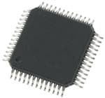
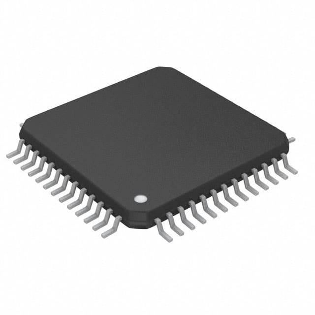
| 供应商器件封装 | 52-MQFP(10x10) |
| 包装 | 托盘 |
| 可用A/D通道 | 4 |
| 可编程输入/输出端数量 | 34 |
| 商标 | Analog Devices |
| 处理器系列 | ADUC836 |
| 外设 | POR,PSM,PWM,温度传感器,WDT |
| 安装风格 | SMD/SMT |
| 定时器数量 | 3 Timer |
| 封装 | Tray |
| 封装/外壳 | 52-QFP |
| 封装/箱体 | QFP-52 |
| 工作温度 | -40°C ~ 125°C |
| 工厂包装数量 | 96 |
| 振荡器类型 | 内部 |
| 接口类型 | I2C/SPI/UART |
| 数据RAM大小 | 2304 B |
| 数据总线宽度 | 8 bit |
| 数据转换器 | A/D 7x16b; D/A 1x12b |
| 最大工作温度 | + 125 C |
| 最大时钟频率 | 1 MHz |
| 最小工作温度 | - 40 C |
| 标准包装 | 1 |
| 核心 | 8052 |
| 核心处理器 | 8052 |
| 核心尺寸 | 8-位 |
| 片上ADC | Yes |
| 片上DAC | With DAC |
| 电压-电源(Vcc/Vdd) | 2.7 V ~ 5.25 V |
| 电源电压-最大 | 5.25 V |
| 电源电压-最小 | 2.7 V |
| 程序存储器大小 | 62 kB |
| 程序存储器类型 | Flash |
| 程序存储容量 | 62KB(62K x 8) |
| 系列 | ADUC836 |
| 输入/输出端数量 | 34 I/O |
| 连接性 | EBI/EMI, I²C, SPI, UART/USART |
| 速度 | 12.58MHz |


- 商务部:美国ITC正式对集成电路等产品启动337调查
- 曝三星4nm工艺存在良率问题 高通将骁龙8 Gen1或转产台积电
- 太阳诱电将投资9.5亿元在常州建新厂生产MLCC 预计2023年完工
- 英特尔发布欧洲新工厂建设计划 深化IDM 2.0 战略
- 台积电先进制程称霸业界 有大客户加持明年业绩稳了
- 达到5530亿美元!SIA预计今年全球半导体销售额将创下新高
- 英特尔拟将自动驾驶子公司Mobileye上市 估值或超500亿美元
- 三星加码芯片和SET,合并消费电子和移动部门,撤换高东真等 CEO
- 三星电子宣布重大人事变动 还合并消费电子和移动部门
- 海关总署:前11个月进口集成电路产品价值2.52万亿元 增长14.8%


PDF Datasheet 数据手册内容提取
MicroConverter®, Dual 16-Bit Sigma-Delta ADCs with Embedded 62 kB Flash MCU ADuC836 FEATURES FUNCTIONAL BLOCK DIAGRAM High Resolution - ADCs 2 Independent ADCs (16-Bit Resolution) AVDD AVDD ADuC836 16-Bit No Missing Codes, Primary ADC CURRENT IEXC1 16-Bit rms (16-Bit p-p) Effective Resolution @ 20 Hz AIN1 SOURCE IEXC2 Offset Drift 10 nV/C, Gain Drift 0.5 ppm/C AIN2 MUX BUF PGA 16-BPRITI M-AR AYDC 12-BIT Memory DAC BUF DAC 62 Kbytes On-Chip Flash/EE Program Memory AIN3 AGND DUAL 4F lKasbhy/tEeEs ,O 1n0-0C Yheiapr FRlaestehn/EtiEo nD, a1t0a0 M Kecmycolersy Endurance AAIINN45 MUX 16A-BUITX IL-IA RAYDC 1-6- DBAITC MUX PWM0 3 Levels of Flash/EE Program Memory Security SETENMSOPR 1D6U-BAILT PWM1 PWM In-Circuit Serial Download (No External Hardware) REFIN– EXTERNAL INTERNAL H23ig0h4 SBpyteeesd O Uns-eCrh Dipo wDantlao aRdA (M5 Seconds) REFIN+ DEVTREECFT BANVRDE GFAP 8051-BASED MCU WITH ADDITIONAL PERIPHERALS 8051 Based Core RESET 62 KBYTES FLASH/EE PROGRAM MEMORY 4 KBYTES FLASH/EE DATA MEMORY 8051 Compatible Instruction Set DVDD POR 2304 BYTES USER RAM 32 kHz External Crystal DGND PLL AND PROG 3 16 BIT TIMERS POWER SUPPLY MON On-Chip Programmable PLL (12.58 MHz Max) CLOCK DIV BAUD RATE TIMER WATCHDOG TIMER 3 16-Bit Timer/Counter OSC R WTAC KTEIM-UEPR/ 4 PPOARRTASLLEL UARSTE, SRPIAI,L A IN/OD I2C 26 Programmable I/O Lines 11 Interrupt Sources, 2 Priority Levels XTAL1 XTAL2 Dual Data Pointer, Extended 11-Bit Stack Pointer On-Chip Peripherals Internal Power on Reset Circuit GENERAL DESCRIPTION 12-Bit Voltage Output DAC The ADuC836 is a complete smart transducer front end, integrating Dual 16-Bit - DACs/PWMs two high resolution - ADCs, an 8-bit MCU, and program/data On-Chip Temperature Sensor Flash/EE memory on a single chip. Dual Excitation Current Sources The two independent ADCs (primary and auxiliary) include a Time Interval Counter (Wake-Up/RTC Timer) temperature sensor and a PGA (allowing direct measurement UART, SPI®, and I2C® Serial I/O of low level signals). The ADCs with on-chip digital filtering and High Speed Baud Rate Generator (Including 115,200) programmable output data rates are intended for the measure- Watchdog Timer (WDT) ment of wide dynamic range, low frequency signals, such as those Power Supply Monitor (PSM) in weigh scale, strain gage, pressure transducer, or temperature Power measurement applications. Normal: 2.3 mA Max @ 3.6 V (Core CLK = 1.57 MHz) The device operates from a 32 kHz crystal with an on-chip PLL Power-Down: 20 A Max with Wake-Up Timer Running generating a high frequency clock of 12.58 MHz. This clock is Specified for 3 V and 5 V Operation routed through a programmable clock divider from which the MCU Package and Temperature Range core clock operating frequency is generated. The microcontroller 52-Lead MQFP (14 mm 14 mm), –40C to +125C core is an 8052 and therefore 8051 instruction set compatible 56-Lead LFCSP (8 mm 8 mm), –40C to +85C with 12 core clock periods per machine cycle. APPLICATIONS 62 Kbytes of nonvolatile Flash/EE program memory, 4 Kbytes of Intelligent Sensors nonvolatile Flash/EE data memory, and 2304 bytes of data RAM Weigh Scales are provided on-chip. The program memory can be configured as Portable Instrumentation, Battery-Powered Systems data memory to give up to 60 Kbytes of NV data memory in data 4–20 mA Transmitters logging applications. Data Logging Precision System Monitoring On-chip factory firmware supports in-circuit serial download and debug modes (via UART), as well as single-pin emulation mode via the EA pin. The ADuC836 is supported by a QuickStart™ development system featuring low cost software and hardware REV. B development tools. Document Feedback Information furnished by Analog Devices is believed to be accurate and reliable. However, no responsibility is assumed by Analog Devices for its use, nor for any infringements of patents or other rights of third parties that may result from its use. No license is granted by implication or other- One Technology Way, P.O. Box 9106, Norwood, MA 02062-9106, U.S.A. wise under any patent or patent rights of Analog Devices.T rademarks and Tel: 781.329.4700 © 2003–2016 Analog Devices, Inc. All rights reserved. registered trademarks are the property of their respective companies. Technical Support www.analog.com
ADuC836 ADuC836 TABLE OF CONTENTS FEATURES . . . . . . . . . . . . . . . . . . . . . . . . . . . . . . . . . . . . . .1 NONVOLATILE FLASH/EE MEMORY Flash/EE Memory Overview . . . . . . . . . . . . . . . . . . . . . . . .29 APPLICATIONS . . . . . . . . . . . . . . . . . . . . . . . . . . . . . . . . . .1 Flash/EE Memory and the ADuC836 . . . . . . . . . . . . . . . . .29 FUNCTIONAL BLOCK DIAGRAM . . . . . . . . . . . . . . . . . .1 ADuC836 Flash/EE Memory Reliability . . . . . . . . . . . . . . .29 Flash/EE Program Memory . . . . . . . . . . . . . . . . . . . . . . . .30 GENERAL DESCRIPTION . . . . . . . . . . . . . . . . . . . . . . . . .1 Serial Downloading . . . . . . . . . . . . . . . . . . . . . . . . . . . . . . .30 SPECIFICATIONS . . . . . . . . . . . . . . . . . . . . . . . . . . . . . . . .3 Parallel Programming . . . . . . . . . . . . . . . . . . . . . . . . . . . . .30 User Download Mode (ULOAD) . . . . . . . . . . . . . . . . . . . .31 ABSOLUTE MAXIMUM RATINGS . . . . . . . . . . . . . . . . .9 Flash/EE Program Memory Security . . . . . . . . . . . . . . . . . .31 ORDERING GUIDE . . . . . . . . . . . . . . . . . . . . . . . . . . . . . . .9 Lock, Secure, and Serial Safe Modes . . . . . . . . . . . . . . . . . .31 Using the Flash/EE Data Memory . . . . . . . . . . . . . . . . . . .32 PIN CONFIGURATIONS . . . . . . . . . . . . . . . . . . . . . . . . . . .9 ECON . . . . . . . . . . . . . . . . . . . . . . . . . . . . . . . . . . . . . . . .32 DETAILED BLOCK DIAGRAM . . . . . . . . . . . . . . . . . . . .10 Programming the Flash/EE Data Memory . . . . . . . . . . . . .33 Flash/EE Memory Timing . . . . . . . . . . . . . . . . . . . . . . . . . .33 PIN FUNCTION DESCRIPTIONS . . . . . . . . . . . . . . . . . .10 OTHER ON-CHIP PERIPHERALS MEMORY ORGANIZATION . . . . . . . . . . . . . . . . . . . . . . .13 DAC . . . . . . . . . . . . . . . . . . . . . . . . . . . . . . . . . . . . . . . . .34 SPECIAL FUNCTION REGISTERS (SFRS) . . . . . . . . . .14 PWM . . . . . . . . . . . . . . . . . . . . . . . . . . . . . . . . . . . . . . . . .36 Accumulator SFR (ACC) . . . . . . . . . . . . . . . . . . . . . . . . . .14 On-Chip PLL . . . . . . . . . . . . . . . . . . . . . . . . . . . . . . . . . .39 B SFR (B) . . . . . . . . . . . . . . . . . . . . . . . . . . . . . . . . . . . . . .14 Time Interval Counter (Wake-Up/RTC Timer) . . . . . . . . .40 Data Pointer (DPTR) . . . . . . . . . . . . . . . . . . . . . . . . . . . . .14 Watchdog Timer . . . . . . . . . . . . . . . . . . . . . . . . . . . . . . . . .42 Stack Pointer (SP and SPH) . . . . . . . . . . . . . . . . . . . . . . . .15 Power Supply Monitor . . . . . . . . . . . . . . . . . . . . . . . . . . . .43 Program Status Word (PSW) . . . . . . . . . . . . . . . . . . . . . . . .15 Serial Peripheral Interface (SPI) . . . . . . . . . . . . . . . . . . . . .44 Power Control SFR (PCON) . . . . . . . . . . . . . . . . . . . . . . .15 I2C Serial Interface . . . . . . . . . . . . . . . . . . . . . . . . . . . . . . .46 ADuC836 Configuration SFR (CFG836) . . . . . . . . . . . . . .15 Dual Data Pointer . . . . . . . . . . . . . . . . . . . . . . . . . . . . . . .48 Complete SFR Map . . . . . . . . . . . . . . . . . . . . . . . . . . . . . .16 8052 COMPATIBLE ON-CHIP PERIPHERALS ADC SFR INTERFACE Parallel I/O Ports 0–3 . . . . . . . . . . . . . . . . . . . . . . . . . . . . .49 ADCSTAT . . . . . . . . . . . . . . . . . . . . . . . . . . . . . . . . . . . . .17 Timers/Counters . . . . . . . . . . . . . . . . . . . . . . . . . . . . . . . . .52 ADCMODE . . . . . . . . . . . . . . . . . . . . . . . . . . . . . . . . . . . .18 UART Serial Interface . . . . . . . . . . . . . . . . . . . . . . . . . . . .57 ADC0CON . . . . . . . . . . . . . . . . . . . . . . . . . . . . . . . . . . . .19 UART Operating Modes . . . . . . . . . . . . . . . . . . . . . . . . . . .57 ADC1CON . . . . . . . . . . . . . . . . . . . . . . . . . . . . . . . . . . . .19 Baud Rate Generation Using Timer 1 and Timer 2 . . . . . . .59 ADC0H/ADC0M/ADC1H/ADC1L . . . . . . . . . . . . . . . . . .20 Baud Rate Generation Using Timer 3 . . . . . . . . . . . . . . . . .60 OF0H/OF0M/OF1H/OF1L . . . . . . . . . . . . . . . . . . . . . . . .20 Interrupt System . . . . . . . . . . . . . . . . . . . . . . . . . . . . . . . . .61 GN0H/GN0M/GN1H/GN1L . . . . . . . . . . . . . . . . . . . . . . .20 HARDWARE DESIGN CONSIDERATIONS SF . . . . . . . . . . . . . . . . . . . . . . . . . . . . . . . . . . . . . . . . . . . .21 External Memory Interface . . . . . . . . . . . . . . . . . . . . . . . . .63 ICON . . . . . . . . . . . . . . . . . . . . . . . . . . . . . . . . . . . . . . . . .21 Power Supplies . . . . . . . . . . . . . . . . . . . . . . . . . . . . . . . . . .64 PRIMARY AND AUXILIARY ADC NOISE Power-On Reset (POR) Operation . . . . . . . . . . . . . . . . . . .64 PERFORMANCE . . . . . . . . . . . . . . . . . . . . . . . . . . . . . .22 Power Consumption . . . . . . . . . . . . . . . . . . . . . . . . . . . . . .64 Power Saving Modes . . . . . . . . . . . . . . . . . . . . . . . . . . . . . .65 PRIMARY AND AUXILIARY ADC CIRCUIT Wake-Up from Power-Down Latency . . . . . . . . . . . . . . . . .65 DESCRIPTION Grounding and Board Layout Recommendations . . . . . . . .66 Overview . . . . . . . . . . . . . . . . . . . . . . . . . . . . . . . . . . . . . . .23 ADuC836 System Self-Identification . . . . . . . . . . . . . . . . . .66 Primary ADC . . . . . . . . . . . . . . . . . . . . . . . . . . . . . . . . . . .23 Clock Oscillator . . . . . . . . . . . . . . . . . . . . . . . . . . . . . . . . .66 Auxiliary ADC . . . . . . . . . . . . . . . . . . . . . . . . . . . . . . . . . .24 Analog Input Channels . . . . . . . . . . . . . . . . . . . . . . . . . . . .24 OTHER HARDWARE CONSIDERATIONS Primary and Auxiliary ADC Inputs . . . . . . . . . . . . . . . . . . .25 In-Circuit Serial Download Access . . . . . . . . . . . . . . . . . . .67 Analog Input Ranges . . . . . . . . . . . . . . . . . . . . . . . . . . . . . .25 Embedded Serial Port Debugger . . . . . . . . . . . . . . . . . . . . .67 Programmable Gain Amplifier . . . . . . . . . . . . . . . . . . . . . . .25 Single-Pin Emulation Mode . . . . . . . . . . . . . . . . . . . . . . . .67 Bipolar/Unipolar Inputs . . . . . . . . . . . . . . . . . . . . . . . . . . .25 Typical System Configuration . . . . . . . . . . . . . . . . . . . . . . .68 Reference Input . . . . . . . . . . . . . . . . . . . . . . . . . . . . . . . . .26 Burnout Currents . . . . . . . . . . . . . . . . . . . . . . . . . . . . . . . .26 QUICKSTART DEVELOPMENT SYSTEM . . . . . . . . . . .69 Excitation Currents . . . . . . . . . . . . . . . . . . . . . . . . . . . . . . .26 TIMING SPECIFICATIONS . . . . . . . . . . . . . . . . . . . . . . .70 Reference Detect . . . . . . . . . . . . . . . . . . . . . . . . . . . . . . . . .26 - Modulator . . . . . . . . . . . . . . . . . . . . . . . . . . . . . . . . . .26 OUTLINE DIMENSIONS . . . . . . . . . . . . . . . . . . . . . . . . .80 Digital Filter . . . . . . . . . . . . . . . . . . . . . . . . . . . . . . . . . . . .27 ADC Chopping . . . . . . . . . . . . . . . . . . . . . . . . . . . . . . . . . .28 Calibration . . . . . . . . . . . . . . . . . . . . . . . . . . . . . . . . . . . . .28 –2– REV. B REV. A –3–
ADuC836 ADuC836 (AV = 2.7 V to 3.6 V or 4.75 V to 5.25 V, DV = 2.7 V to 3.6 V or 4.75 V to 5.25 V, DD DD S PECIFICATIONS1 REFIN(+) = 2.5 V; REFIN(–) = AGND; AGND = DGND = 0 V; XTAL1/XTAL2 = 32.768 kHz Crystal; all specifications T to T , unless otherwise noted.) MIN MAX Parameter ADuC836 Test Conditions/Comments Unit ADC SPECIFICATIONS Conversion Rate 5.4 On Both Channels Hz min 105 Programmable in 0.732 ms Increments Hz max Primary ADC No Missing Codes2 16 20 Hz Update Rate Bits min Resolution 13.5 Range = ±20 mV, 20 Hz Update Rate Bits p-p typ 16 Range = ±2.56 V, 20 Hz Update Rate Bits p-p typ Output Noise See Tables X and XI in Output Noise Varies with Selected ADuC836 ADC Description Update Rate and Gain Range Integral Nonlinearity ±15 1 LSB ppm of FSR max Offset Error3 ±3 V typ Offset Error Drift ±10 nV/°C typ Full-Scale Error4 ±10 Range = ±20 mV to ±640 mV V typ ±0.5 Range = ±1.28 V to ±2.56 V LSB typ Gain Error Drift5 ±0.5 ppm/°C typ ADC Range Matching ±2 AIN = 18 mV V typ Power Supply Rejection (PSR) 95 AIN = 7.8 mV, Range = ±20 mV dBs typ 80 AIN = 1 V, Range = ±2.56 V dBs typ Common-Mode DC Rejection On AIN 95 At DC, AIN = 7.8 mV, Range = ±20 mV dBs typ 113 At DC, AIN = 1 V, Range = ±2.56 V dBs typ On REFIN 125 At DC, AIN = 1 V, Range = ±2.56 V dBs typ Common-Mode 50 Hz/60 Hz Rejection 20 Hz Update Rate On AIN 95 50 Hz/60 Hz ±1 Hz, AIN = 7.8 mV, dBs typ Range = ±20 mV 90 50 Hz/60 Hz ±1 Hz, AIN = 1 V, dBs typ Range = ±2.56 V On REFIN 90 50 Hz/60 Hz ±1 Hz, AIN = 1 V, dBs typ Range = ±2.56 V Normal Mode 50 Hz/60 Hz Rejection On AIN 60 50 Hz/60 Hz ±1 Hz, 20 Hz Update Rate dBs typ On REFIN 60 50 Hz/60 Hz ±1 Hz, 20 Hz Update Rate dBs typ Auxiliary ADC No Missing Codes2 16 Bits min Resolution 16 Range = ±2.5 V, 20 Hz Update Rate Bits p-p typ Output Noise See Table XII in ADuC836 Output Noise Varies with Selected ADC Description Update Rate Integral Nonlinearity ±15 ppm of FSR max Offset Error3 –2 LSB typ Offset Error Drift 1 V/°C typ Full-Scale Error6 –2.5 LSB typ Gain Error Drift5 ±0.5 ppm/°C typ Power Supply Rejection (PSR) 80 AIN = 1 V, 20 Hz Update Rate dBs typ Normal Mode 50 Hz/60 Hz Rejection On AIN 60 50 Hz/60 Hz ±1 Hz dBs typ On REFIN 60 50 Hz/60 Hz ±1 Hz, 20 Hz Update Rate dBs typ DAC PERFORMANCE DC Specifications7 Resolution 12 Bits Relative Accuracy ±3 LSB typ Differential Nonlinearity –1 Guaranteed 12-Bit Monotonic LSB max Offset Error ±50 mV max Gain Error8 ±1 AV Range % max DD ±1 V Range % typ REF AC Specifications2, 7 Voltage Output Settling Time 15 Settling Time to 1 LSB of Final Value s typ Digital-to-Analog Glitch Energy 10 1 LSB Change at Major Carry nVs typ –2– REV. A REV. B –3–
ADuC836 ADuC836 SPECIFICATIONS (continued) Parameter ADuC836 Test Conditions/Comments Unit INTERNAL REFERENCE ADC Reference Reference Voltage 1.25 ± 1% Initial Tolerance @ 25°C, V = 5 V V min/max DD Power Supply Rejection 45 dBs typ Reference Tempco 100 ppm/°C typ DAC Reference Reference Voltage 2.5 ± 1% Initial Tolerance @ 25°C, V = 5 V V min/max DD Power Supply Rejection 50 dBs typ Reference Tempco ±100 ppm/°C typ ANALOG INPUTS/REFERENCE INPUTS Primary ADC Differential Input Voltage Ranges9, 10 External Reference Voltage = 2.5 V RN2, RN1, RN0 of ADC0CON Set to Bipolar Mode (ADC0CON3 = 0) ±20 0 0 0 (Unipolar Mode 0 mV to 20 mV) mV ±40 0 0 1 (Unipolar Mode 0 mV to 40 mV) mV ±80 0 1 0 (Unipolar Mode 0 mV to 80 mV) mV ±160 0 1 1 (Unipolar Mode 0 mV to 160 mV) mV ±320 1 0 0 (Unipolar Mode 0 mV to 320 mV) mV ±640 1 0 1 (Unipolar Mode 0 mV to 640 mV) mV ±1.28 1 1 0 (Unipolar Mode 0 V to 1.28 V) V ±2.56 1 1 1 (Unipolar Mode 0 V to 2.56 V) V Analog Input Current2 ±1 T = 85°C nA max MAX ±5 T = 125°C nA max MAX Analog Input Current Drift ±5 T = 85°C pA/°C typ MAX ±15 T = 125°C pA/°C typ MAX Absolute AIN Voltage Limits2 AGND + 100 mV V min AV – 100 mV V max DD Auxiliary ADC Input Voltage Range9, 10 0 to V Unipolar Mode, for Bipolar Mode V REF See Note 11 Average Analog Input Current 125 Input Current Will Vary with Input nA/V typ Average Analog Input Current Drift2 ±2 Voltage on the Unbuffered Auxiliary ADC pA/V/°C typ Absolute AIN Voltage Limits2, 11 AGND – 30 mV V min AV + 30 mV V max DD External Reference Inputs REFIN(+) to REFIN(–) Range2 1 V min AV V max DD Average Reference Input Current 1 Both ADCs Enabled A/V typ Average Reference Input Current Drift ±0.1 nA/V/°C typ “NO Ext. REF” Trigger Voltage 0.3 NOXREF Bit Active if V < 0.3 V V min REF 0.65 NOXREF Bit Inactive if V > 0.65 V V max REF ADC SYSTEM CALIBRATION Full-Scale Calibration Limit 1.05 FS V max Zero-Scale Calibration Limit –1.05 FS V min Input Span 0.8 FS V min 2.1 FS V max ANALOG (DAC) OUTPUT Voltage Range 0 to V DACRN = 0 in DACCON SFR V typ REF 0 to AV DACRN = 1 in DACCON SFR V typ DD Resistive Load 10 From DAC Output to AGND k typ Capacitive Load 100 From DAC Output to AGND pF typ Output Impedance 0.5 typ I 50 A typ SINK TEMPERATURE SENSOR Accuracy ±2 °C typ Thermal Impedance ( ) 90 MQFP Package °C/W typ JA 52 CSP Package (Base Floating)12 °C/W typ –4– REV. B REV. A –5–
ADuC836 ADuC836 Parameter ADuC836 Test Conditions/Comments Unit TRANSDUCER BURNOUT CURRENT SOURCES AIN+ Current –100 AIN+ Is the Selected Positive Input nA typ to the Primary ADC AIN– Current +100 AIN– Is the Selected Negative Input nA typ to the Auxiliary ADC Initial Tolerance @ 25°C ±10 % typ Drift 0.03 %/°C typ EXCITATION CURRENT SOURCES Output Current –200 Available from Each Current Source A typ Initial Tolerance @ 25°C ±10 % typ Drift 200 ppm/°C typ Initial Current Matching @ 25°C ±1 Matching between Both Current Sources % typ Drift Matching 20 ppm/°C typ Line Regulation (AV ) 1 AV = 5 V + 5% A/V typ DD DD Load Regulation 0.1 A/V typ Output Compliance2 AV – 0.6 V max DD AGND V min LOGIC INPUTS All Inputs Except SCLOCK, RESET, and XTAL12 V , Input Low Voltage 0.8 DV = 5 V V max INL DD 0.4 DV = 3 V V max DD V , Input High Voltage 2.0 V min INH SCLOCK and RESET Only (Schmitt-Triggered Inputs)2 V 1.3/3 DV = 5 V V min/V max T+ DD 0.95/2.5 DV = 3 V V min/V max DD V 0.8/1.4 DV = 5 V V min/V max T– DD 0.4/1.1 DV = 3 V V min/V max DD V V 0.3/0.85 DV = 5 V V min/V max T+ – T– DD 0.3/0.85 DV = 3 V V min/V max DD Input Currents Port 0, P1.2–P1.7, EA ±10 V = 0 V or V A max IN DD SCLOCK, MOSI, MISO, SS13 –10 min, –40 max V = 0 V, DV = 5 V, Internal Pull-Up A min/A max IN DD ±10 V = V , DV = 5 V A max IN DD DD RESET ±10 V = 0 V, DV = 5 V A max IN DD 35 min, 105 max V = V , DV = 5 V, A min/A max IN DD DD Internal Pull-Down P1.0, P1.1, Ports 2 and 3 ±10 V = V , DV = 5 V A max IN DD DD –180 V = 2 V, DV = 5 V A min IN DD –660 A max –20 V = 450 mV, DV = 5 V A min IN DD –75 A max Input Capacitance 5 All Digital Inputs pF typ CRYSTAL OSCILLATOR (XTAL1 AND XTAL2) Logic Inputs, XTAL1 Only2 V , Input Low Voltage 0.8 DV = 5 V V max INL DD 0.4 DV = 3 V V max DD V , Input High Voltage 3.5 DV = 5 V V min INH DD 2.5 DV = 3 V V min DD XTAL1 Input Capacitance 18 pF typ XTAL2 Output Capacitance 18 pF typ –4– REV. A REV. B –5–
ADuC836 ADuC836 SPECIFICATIONS (continued) Parameter ADuC836 Test Conditions/Comments Unit LOGIC OUTPUTS (Not Including XTAL2)2 V , Output High Voltage 2.4 V = 5 V, I = 80 A V min OH DD SOURCE 2.4 V = 3 V, I = 20 A V min DD SOURCE V , Output Low Voltage14 0.4 I = 8 mA, SCLOCK, MOSI/SDATA V max OL SINK 0.4 I = 10 mA, P1.0 and P1.1 V max SINK 0.4 I = 1.6 mA, All Other Outputs V max SINK Floating State Leakage Current2 ±10 A max Floating State Output Capacitance 5 pF typ POWER SUPPLY MONITOR (PSM) AV Trip Point Selection Range 2.63 Four Trip Points Selectable in This Range V min DD 4.63 Programmed via TPA1–0 in PSMCON V max AV Power Supply Trip Point Accuracy ±3.0 T = 85°C % max DD MAX ±4.0 T = 125°C % max MAX DV Trip Point Selection Range 2.63 Four Trip Points Selectable in This Range V min DD 4.63 Programmed via TPD1–0 in PSMCON V max DV Power Supply Trip Point Accuracy ±3.0 T = 85C % max DD MAX ±4.0 T = 125C % max MAX WATCHDOG TIMER (WDT) Timeout Period 0 Nine Timeout Periods in This Range ms min 2000 Programmed via PRE3–0 in WDCON ms max MCU CORE CLOCK RATE Clock Rate Generated via On-Chip PLL MCU Clock Rate2 98.3 Programmable via CD2–0 Bits in kHz min PLLCON SFR 12.58 MHz max START-UP TIME At Power-On 300 ms typ After External RESET in Normal Mode 3 ms typ After WDT Reset in Normal Mode 3 Controlled via WDCON SFR ms typ From Idle Mode 10 s typ From Power-Down Mode Oscillator Running OSC_PD Bit = 0 in PLLCON SFR Wake-Up with INT0 Interrupt 20 s typ Wake-Up with SPI Interrupt 20 s typ Wake-Up with TIC Interrupt 20 s typ Wake-Up with External RESET 3 ms typ Oscillator Powered Down OSC_PD Bit = 1 in PLLCON SFR Wake-Up with INT0 Interrupt 20 s typ Wake-Up with SPI Interrupt 20 s typ Wake-Up with External RESET 5 ms typ FLASH/EE MEMORY RELIABILITY CHARACTERISTICS15 Endurance16 100,000 Cycles min Data Retention17 100 Years min –6– REV. B REV. A –7–
ADuC836 ADuC836 Parameter ADuC836 Test Conditions/Comments Unit POWER REQUIREMENTS DV and AV Can Be Set Independently DD DD Power Supply Voltages AV , 3 V Nominal Operation 2.7 V min DD 3.6 V max AV , 5 V Nominal Operation 4.75 V min DD 5.25 V max DV , 3 V Nominal Operation 2.7 V min DD 3.6 V max DV , 5 V Nominal Operation 4.75 V min DD 5.25 V max 5 V POWER CONSUMPTION DV = 4.75 V to 5.25 V, AV = 5.25 V DD DD Power Supply Currents Normal Mode18, 19 DV Current 4 Core CLK = 1.57 MHz mA max DD DV Current 13 Core CLK = 12.58 MHz mA typ DD 16 Core CLK = 12.58 MHz mA max AV Current 180 Core CLK = 1.57 MHz or 12.58 MHz A max DD Power Supply Currents Power-Down Mode18, 19 Core CLK = 1.57 MHz or 12.58 MHz DV Current 53 T = 85°C; Osc. On, TIC On A max DD MAX 100 T = 125°C; Osc. On, TIC On A max MAX DV Current 30 T = 85°C; Osc. Off A max DD MAX 80 T = 125°C; Osc. Off A max MAX AV Current 1 T = 85°C; Osc. On or Osc. Off A max DD MAX 3 T = 125°C; Osc. On or Osc. Off A max MAX Typical Additional Power Supply Currents Core CLK = 1.57 MHz (AI and DI ) DD DD PSM Peripheral 50 A typ Primary ADC 1 mA typ Auxiliary ADC 500 A typ DAC 150 A typ Dual Current Sources 400 A typ 3 V POWER CONSUMPTION DV = 2.7 V to 3.6 V DD Power Supply Currents Normal Mode18, 19 DV Current 2.3 Core CLK = 1.57 MHz mA max DD DV Current 8 Core CLK = 12.58 MHz mA typ DD 10 Core CLK = 12.58 MHz mA max AV Current 180 AV = 5.25 V, Core CLK = 1.57 MHz DD DD or 12.58 MHz A max Power Supply Currents Power-Down Mode18, 19 Core CLK = 1.57 MHz or 12.58 MHz DV Current 20 T = 85°C; Osc. On, TIC On A max DD MAX 40 T = 125°C; Osc. On, TIC On A max MAX DV Current 10 Osc. Off A typ DD AV Current 1 AV = 5.25 V; T = 85°C; DD DD MAX Osc. On or Osc. Off A max 3 AV = 5.25 V; T = 125°C; DD MAX Osc. On or Osc. Off A max –6– REV. A REV. B –7–
ADuC836 ADuC836 NOTES 1 Temperature range for ADuC836BS (MQFP package) is –40°C to +125°C. Temperature range for ADuC836BCP (CSP package) is –40°C to +85°C. 2 These numbers are not production tested but are guaranteed by design and/or characterization data on production release. 3 System Zero-Scale Calibration can remove this error. 4 The primary ADC is factory calibrated at 25°C with AV = DV = 5 V yielding this full-scale error of 10 V. If user power supply or temperature conditions are significantly DD DD different from these, an Internal Full-Scale Calibration will restore this error to 10 V. A system zero-scale and full-scale calibration will remove this error altogether. 5 Gain Error Drift is a span drift. To calculate Full-Scale Error Drift, add the Offset Error Drift to the Gain Error Drift times the full-scale input. 6 The auxiliary ADC is factory calibrated at 25°C with AV = DV = 5 V yielding this full-scale error of –2.5 LSB. A system zero-scale and full-scale calibration DD DD will remove this error altogether. 7 DAC linearity and ac specifications are calculated using: reduced code range of 48 to 4095, 0 to V ; reduced code range of 100 to 3950, 0 to V . REF DD 8 Gain Error is a measurement of the span error of the DAC. 9 In general terms, the bipolar input voltage range to the primary ADC is given by Range = ±(V 2RN)/125, where: ADC REF V = REFIN(+) to REFIN(–) voltage and V = 1.25 V when internal ADC V is selected. RN = decimal equivalent of RN2, RN1, RN0, e.g., REF REF REF V = 2.5 V and RN2, RN1, RN0 = 1, 1, 0 the Range = ±1.28 V. In Unipolar mode, the effective range is 0 V to 1.28 V in our example. REF ADC 101.25 V is used as the reference voltage to the auxiliary ADC when internal V is selected via XREF0 and XREF1 bits in ADC0CON and ADC1CON, respectively. REF 11In Bipolar mode, the auxiliary ADC can only be driven to a minimum of AGND – 30 mV as indicated by the auxiliary ADC absolute AIN voltage limits. The bipolar range is still –V to +V ; however, the negative voltage is limited to –30 mV. REF REF 12 The ADuC836BCP (CSP package) has been qualified and tested with the base of the CSP package floating. 13Pins configured in SPI mode, pins configured as digital inputs during this test. 14Pins configured in I2C mode only. 15Flash/EE Memory Reliability Characteristics apply to both the Flash/EE program memory and Flash/EE data memory. 16Endurance is qualified to 100 Kcycles as per JEDEC Std. 22 method A117 and measured at –40°C, +25°C, +85°C, and +125°C. Typical endurance at 25°C is 700 Kcycles. 17Retention lifetime equivalent at junction temperature (T) = 55°C as per JEDEC Std. 22, Method A117. Retention lifetime based on an activation energy of 0.6 eV will J derate with junction temperature as shown in Figure 16 in the Flash/EE Memory section. 18Power Supply current consumption is measured in Normal, Idle, and Power-Down modes under the following conditions: Normal mode: Reset = 0.4 V, Digital I/O pins = open circuit, Core Clk changed via CD bits in PLLCON, Core Executing internal software loop. Idle mode: Reset = 0.4 V, Digital I/O pins = open circuit, Core Clk changed via CD bits in PLLCON, PCON.0 = 1, Core Execution suspended in idle mode. Power-Down mode: Reset = 0.4 V, All P0 pins and P1.2–P1.7 pins = 0.4 V, all other digital I/O pins are open circuit, Core Clk changed via CD bits in PLLCON, PCON.1 = 1, Core Execution suspended in Power-Down mode, OSC turned on or off via OSC_PD bit (PLLCON.7) in PLLCON SFR. 19DV power supply current will increase typically by 3 mA (3 V operation) and 10 mA (5 V operation) during a Flash/EE memory program or erase cycle. DD Specifications subject to change without notice. –8– REV. B REV. A –9–
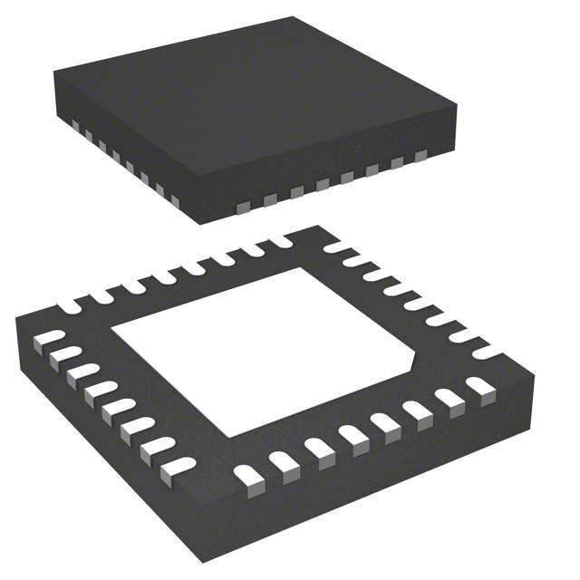
ADuC836 ADuC836 ABSOLUTE MAXIMUM RATINGS1 PIN CONFIGURATIONS (TA= 25°C, unless otherwise noted.) 52-Lead MQFP AV to AGND . . . . . . . . . . . . . . . . . . . . . . . . . –0.3 V to +7 V DD �� �� AV to DGND . . . . . . . . . . . . . . . . . . . . . . . . . –0.3 V to +7 V DD DV to AGND . . . . . . . . . . . . . . . . . . . . . . . . . –0.3 V to +7 V DD DVDD to DGND . . . . . . . . . . . . . . . . . . . . . . . . –0.3 V to +7 V � ������ �� AGND to DGND2 . . . . . . . . . . . . . . . . . . . . . . –0.3 V to +0.3 V ���������� AV to DV . . . . . . . . . . . . . . . . . . . . . . . . . . . . –2 V to +5 V DD DD Analog Input Voltage to AGND3 . . . . . . –0.3 V to AV + 0.3 V ������� DD Reference Input Voltage to AGND . . . . –0.3 V to AV + 0.3 V �������� DD �������������� AIN/REFIN Current (Indefinite) . . . . . . . . . . . . . . . . . . 30 mA Digital Input Voltage to DGND . . . . . . –0.3 V to DV + 0.3 V DD Digital Output Voltage to DGND . . . . . –0.3 V to DV + 0.3 V �� �� DD Operating Temperature Range . . . . . . . . . . . . –40°C to +125°C Storage Temperature Range . . . . . . . . . . . . . . –65°C to +150°C �� �� Junction Temperature . . . . . . . . . . . . . . . . . . . . . . . . . . . 150°C Thermal Impedance (MQFP) . . . . . . . . . . . . . . . . . 90°C/W JA JA Thermal Impedance (LFCSP Base Floating) . . . . . . 52°C/W 56-Lead LFCSP Lead Temperature, Soldering Vapor Phase (60 sec) . . . . . . . . . . . . . . . . . . . . . . . . . . 215°C �� �� Infrared (15 sec) . . . . . . . . . . . . . . . . . . . . . . . . . . . . . 220°C � ������ �� ���������� NOTES 1Stresses above those listed under Absolute Maximum Ratings may cause permanent damage to the device. This is a stress rating only; functional operation of the device ������� at these or any other conditions above those listed in the operational sections of this �������� specification is not implied. Exposure to absolute maximum rating conditions for �������������� extended periods may affect device reliability. 2AGND and DGND are shorted internally on the ADuC836. 3Applies to P1.2 to P1.7 pins operating in analog or digital input modes. �� �� �� �� NOTES 1. THE LFCSP HAS AN EXPOSED PAD THAT MUST BE SOLDERED TO THE METAL PLATE ON THE PRINTED CIRCUIT BOARD (PCB) FOR MECHANICAL REASONS AND TO DGND. CAUTION ESD (electrostatic discharge) sensitive device. Electrostatic charges as high as 4000 V readily accumulate on the human body and test equipment and can discharge without detection. Although the ADuC836 features proprietary ESD protection circuitry, permanent damage may occur on devices subjected to high energy electrostatic discharges. Therefore, proper ESD precautions are recommended to avoid performance degradation or loss of functionality. –8– REV. A REV. B –9–
ADuC836 ADuC836 P0.0 (AD0) P0.1 (AD1) P0.2 (AD2) P0.3 (AD3) P0.4 (AD4) P0.5 (AD5) P0.6 (AD6) P0.7 (AD7) P1.0 (T2) P1.1 (T2EX) P1.2 (DAC/IEXC 1) P1.3 (AIN5/IEXC 2) P1.4 (AIN1) P1.5 (AIN2) P1.6 (AIN3) P1.7 (AIN4/DAC) P2.0 (A8/A16) P2.1 (A9/A17) P2.2 (A10/A18) P2.3 (A11/A19) 12/A20)P2.4 (A P2.5 (A13/A21) P2.6 (A14/A22) 15/A23)P2.7 (A P3.0 (RXD) P3.1 (TXD) P3.2 (INT0) P3.3 (INT1) P3.4 (T0/PWMCLK) P3.5 (T1) P3.6 (WR) P3.7 (RD) 43 44 45 46 49 50 51 52 1 2 3 4 9 10 11 12 28 29 30 31 36 37 38 39 16 17 18 19 22 23 24 25 ADuC836 12-BIT CODNATCROL VOLTAGE BUF 3 DAC OUTPUT DAC ADC AIN1 PRIMARY ADC CONTROL AIN2 MAUINX BUF PGA 1-6- BAIDTC CALIBARNADTION DUAL 16-BIT PWM - DAC 1 PWM0 AIN3 CONTROL MUX AIN4 MAUINX AUXIL16IA-BRIYT ADC ADC CAONNDTROL 1D6U-BAILT 2 PWM1 AIN5 - ADC CALIBRATION PWM SETENMSOPR RBEAFNEDR EGNACPE 62 KBYFTLEASS PHR/EOEG RAM/ 2U3S0E4 RB YRTAEMS 16-BIT 2232 TT01 COUNTER TIMERS 1 T2 WATCHDOG 4 KBYTES DATA TIMER 2 T2EX REFIN VREF FLASH/EE 8052 REFIN DETECT MCU POWMEORN ISTUOPRPLY 2 DATA POINTERS CORE 11-BIT STACK POINTER PLL WITH PROG. 200A 200A CLOCK DIVIDER 18 INT0 DOWNLOADER WAKE-UP/ 19 INT1 DEBUGGER RTC TIMER IEXC 1 CURRENT IEXC 2 SOMUURXCE POR SERUIAALR PTORT TUIAMRETR GLE-PINULATOR S PINI/IT2ECR SFEARCIAEL OSC NM SIE 5 6 20 34 48 47 21 35 15 16 17 41 40 42 26 27 14 13 32 33 AVDD AGND DVDD DGND RESET RXD TXD PSEN EA ALE CLOCK SDATA MISO SS XTAL1 XTAL2 S SI/ O M *PIN NUMBERS REFER TO THE 52-LEAD MQFP PACKAGE SHADED AREAS REPRESENT THE NEW FEATURES OF THE ADuC836 OVER THE ADuC816 Figure 1. Detailed Block Diagram PIN FUNCTION DESCRIPTIONS Pin No. Pin No. 52-Lead 56-Lead MQFP CSP Mnemonic Type* Description 1, 2 56, 1 P1.0/P1.1 I/O P1.0 and P1.1 can function as digital inputs or digital outputs and have a pull-up configuration as described for Port 3. P1.0 and P1.1 have an increased current drive sink capability of 10 mA. P1.0/T2/PWM0 I/O P1.0 and P1.1 also have various secondary functions as described below. P1.0 can be used to provide a clock input to Timer 2. When enabled, Counter 2 is incremented in response to a negative transition on the T2 input pin. If the PWM is enabled, the PWM0 output will appear at this pin. P1.1/T2EX/PWM1 I/O P1.1 can also be used to provide a control input to Timer 2. When enabled, a PWM1 negative transition on the T2EX input pin will cause a Timer 2 capture or reload event. If the PWM is enabled, the PWM1 output will appear at this pin. 3–4, 2–3, P1.2–P1.7 I Port 1.2 to Port 1.7 have no digital output driver; they can function as a digital input 9–12 11–14 for which 0 must be written to the port bit. As a digital input, these pins must be driven high or low externally. These pins also have the following analog functionality: P1.2/DAC/IEXC1 I/O The voltage output from the DAC or one or both current sources (200 µA or 2 200 µA) can be configured to appear at this pin. P1.3/AIN5/IEXC2 I/O Auxiliary ADC input or one or both current sources can be configured at this pin. –10– REV. B REV. A –11–
ADuC836 ADuC836 PIN FUNCTION DESCRIPTIONS (continued) Pin No. Pin No. 52-Lead 56-Lead MQFP CSP Mnemonic Type* Description P1.4/AIN1 I Primary ADC, Positive Analog Input P1.5/AIN2 I Primary ADC, Negative Analog Input P1.6/AIN3 I Auxiliary ADC Input or Muxed Primary ADC, Positive Analog Input P1.7/AIN4/DAC I/O Auxiliary ADC Input or Muxed Primary ADC, Negative Analog Input. The voltage output from the DAC can also be configured to appear at this pin. 5 4, 5 AV S Analog Supply Voltage, 3 V or 5 V DD 6 6, 7, 8 AGND S Analog Ground. Ground reference pin for the analog circuitry. 7 9 REFIN(–) I Reference Input, Negative Terminal 8 10 REFIN(+) I Reference Input, Positive Terminal 13 15 SS I Slave Select Input for the SPI Interface. A weak pull-up is present on this pin. 14 16 MISO I/O Master Input/Slave Output for the SPI Interface. A weak pull-up is present on this input pin. 15 17 RESET I Reset Input. A high level on this pin for 16 core clock cycles while the oscillator is running resets the device. There is an internal weak pull-down and a Schmitt trigger input stage on this pin. 16–19, 18–21, P3.0–P3.7 I/O P3.0–P3.7 are bidirectional port pins with internal pull-up resistors. Port 3 pins that 22–25 24–27 have 1s written to them are pulled high by the internal pull-up resistors, and in that state can be used as inputs. As inputs, Port 3 pins being pulled externally low will source current because of the internal pull-up resistors. When driving a 0-to-1 output transition, a strong pull-up is active for two core clock periods of the instruction cycle. Port 3 pins also have various secondary functions including: P3.0/RXD I/O Receiver Data for UART Serial Port P3.1/TXD I/O Transmitter Data for UART Serial Port P3.2/INT0 I/O External Interrupt 0. This pin can also be used as a gate control input to Timer 0. P3.3/INT1 I/O External Interrupt 1. This pin can also be used as a gate control input to Timer 1. P3.4/T0/PWMCLK I/O Timer/Counter 0 External Input. If the PWM is enabled, an external clock may be input at this pin. P3.5/T1 I/O Timer/Counter 1 External Input P3.6/WR I/O External Data Memory Write Strobe. Latches the data byte from Port 0 into an external data memory. P3.7/RD I/O External Data Memory Read Strobe. Enables the data from an external data memory to Port 0. 20, 34, 48 22, 36, 51, DV S Digital Supply, 3 V or 5 V DD 21, 35, 47 23, 37, 38, DGND S Digital Ground. Ground reference point for the digital circuitry. 50 26 SCLOCK I/O Serial Interface Clock for either the I2C or SPI Interface. As an input, this pin is a Schmitt-triggered input, and a weak internal pull-up is present on this pin unless it is outputting logic low. This pin can also be directly controlled in software as a digital output pin. 27 MOSI/SDATA I/O Serial Data I/O for the I2C Interface or Master Output/Slave Input for the SPI Interface. A weak internal pull-up is present on this pin unless it is outputting logic low. This pin can also be directly controlled in software as a digital output pin. 28–31 30–33 P2.0–P2.7 I/O Port 2 is a bidirectional port with internal pull-up resistors. Port 2 pins that have 1s 36–39 39–42 (A8–A15) written to them are pulled high by the internal pull-up resistors, and in that state can (A16–A23) be used as inputs. As inputs, Port 2 pins being pulled externally low will source current because of the internal pull-up resistors. Port 2 emits the high order address bytes during fetches from external program memory and middle and high order address bytes during accesses to the 24-bit external data memory space. 32 34 XTAL1 I Input to the Crystal Oscillator Inverter 33 35 XTAL2 O Output from the Crystal Oscillator Inverter. (See the Hardware Design Considerations section for description.) –10– REV. A REV. B –11–
ADuC836 ADuC836 PIN FUNCTION DESCRIPTIONS (continued) Pin No. Pin No. 52-Lead 56-Lead MQFP CSP Mnemonic Type* Description 40 43 EA I/O External Access Enable, Logic Input. When held high, this input enables the device to fetch code from internal program memory locations 0000h to F7FFh. When held low, this input enables the device to fetch all instructions from external program memory. To determine the mode of code execution, i.e., internal or external, the EA pin is sampled at the end of an external RESET assertion or as part of a device power cycle. EA may also be used as an external emulation I/O pin, and therefore the voltage level at this pin must not be changed during normal mode operation as it may cause an emulation interrupt that will halt code execution. 41 44 PSEN O Program Store Enable, Logic Output. This output is a control signal that enables the external program memory to the bus during external fetch operations. It is active every six oscillator periods except during external data memory accesses. This pin remains high during internal program execution. PSEN can also be used to enable Serial Download mode when pulled low through a resistor at the end of an external RESET assertion or as part of a device power cycle. 42 45 ALE O Address Latch Enable, Logic Output. This output is used to latch the low byte (and page byte for 24-bit data address space accesses) of the address to external memory during external code or data memory access cycles. It is activated every six oscillator periods except during an external data memory access. It can be disabled by setting the PCON.4 bit in the PCON SFR. 43–46 46–49 P0.0–P0.7 I/O These pins are part of Port 0, which is an 8-bit, open-drain, bidirectional 49–52 52–55 (AD0–AD3) I/O port. Port 0 pins that have 1s written to them float and in that state can be used (AD4–AD7)as high impedance inputs. An external pull-up resistor will be required on P0 outputs to force a valid logic high level externally. Port 0 is also the multiplexed low order address and data bus during accesses to external program or data memory. In this application, it uses strong internal pull-ups when emitting 1s. EPAD Exposed Pad. The LFCSP has an exposed pad that must be soldered to the metal plate on the printed circuit board (PCB) for mechanical reasons and to DGND. * I = Input, O = Output, S = Supply. –12– REV. B REV. A –13–
ADuC836 ADuC836 MEMORY ORGANIZATION Reset initializes the stack pointer to location 07H. Any call or push The ADuC836 contains four different memory blocks: pre-increments the SP before loading the stack. Therefore, loading the stack starts from location 08H, which is also the first register 62 Kbytes of On-Chip Flash/EE Program Memory (R0) of register bank 1. Thus, if one is going to use more than one 4 Kbytes of On-Chip Flash/EE Data Memory register bank, the stack pointer should be initialized to an area of 256 bytes of General-Purpose RAM RAM not used for data storage. 2 Kbytes of Internal XRAM 7FH (1) Flash/EE Program Memory GENERAL-PURPOSE The ADuC836 provides 62 Kbytes of Flash/EE program mem- AREA ory to run user code. The user can choose to run code from this 30H internal memory or run code from an external program memory. BANKS 2FH If the user applies power or resets the device while the EA pin is SELVEICATED B(BITIT-A ADDDDRREESSSSAEBSL)E pulled low externally, the part will execute code from the external BITS IN PSW 20H program space; otherwise, if EA is pulled high externally, the part 1FH defaults to code execution from its internal 62 Kbytes of Flash/EE 11 program memory. 18H 17H Unlike the ADuC816, where code execution can overflow from the 10 internal code space to external code space once the PC becomes 10H FOUR BANKS OF EIGHT REGISTERS greater than 1FFFH, the ADuC836 does not support the rollover 0FH R0–R7 01 from F7FFH in internal code space to F800H in external code 08H space. Instead, the 2048 bytes between F800H and FFFFH will 07H RESET VALUE OF appear as NOP instructions to user code. 00 STACK POINTER 00H Permanently embedded firmware allows code to be serially down- loaded to the 62 Kbytes of internal code space via the UART serial Figure 2. Lower 128 Bytes of Internal Data Memory port while the device is in-circuit. No external hardware is required. (4) Internal XRAM 56 Kbytes of the program memory can be reprogrammed during The ADuC836 contains 2 Kbytes of on-chip extended data mem- runtime; thus the code space can be upgraded in the field using a ory. This memory, although on-chip, is accessed via the MOVX user defined protocol or it can be used as a data memory. This instruction. The 2 Kbytes of internal XRAM are mapped into the is discussed in more detail in the Flash/EE Memory section. bottom 2 Kbytes of the external address space if the CFG836.0 bit is set. Otherwise, access to the external data memory will occur (2) Flash/EE Data Memory just like a standard 8051. 4 Kbytes of Flash/EE Data Memory are available to the user and can be accessed indirectly via a group of registers mapped into the Even with the CFG836.0 bit set, access to the external XRAM Special Function Register (SFR) area. Access to the Flash/EE Data will occur once the 24-bit DPTR is greater than 0007FFH. memory is discussed in detail in the Flash/EE Memory section. FFFFFFH FFFFFFH (3) General-Purpose RAM The general-purpose RAM is divided into two separate memories: the upper and lower 128 bytes of RAM. The lower 128 bytes of RAM can be accessed through direct or indirect addressing; the upper 128 bytes of RAM can only be accessed through indirect EXTERNAL EXTERNAL DATA DATA addressing as it shares the same address space as the SFR space, MEMORY MEMORY SPACE SPACE which can only be accessed through direct addressing. (24-BIT (24-BIT ADDRESS ADDRESS The lower 128 bytes of internal data memory are mapped as shown SPACE) SPACE) in Figure 2. The lowest 32 bytes are grouped into four banks of eight registers addressed as R0 through R7. The next 16 bytes (128 bits), locations 20H through 2FH above the register banks, 000800H form a block of directly addressable bit locations at bit addresses 0007FFH 2 KBYTES 00H through 7FH. The stack can be located anywhere in the inter- ON-CHIP XRAM nal memory address space, and the stack depth can be expanded 000000H 000000H up to 2048 bytes. CFG836.0 = 0 CFG836.0 = 1 Figure 3. Internal and External XRAM GENERAL NOTES PERTAINING TO THIS DATA SHEET 1. SET implies a Logic 1 state and CLEARED implies a Logic 0 state, unless otherwise stated. 2. SET and CLEARED also imply that the bit is set or automatically cleared by the ADuC836 hardware, unless otherwise stated. 3. User software should not write 1s to reserved or unimplemented bits as they may be used in future products. 4. Any pin numbers used throughout this data sheet refer to the 52-lead MQFP package, unless otherwise stated. –12– REV. A REV. B –13–
ADuC836 ADuC836 When accessing the internal XRAM, the P0 and P2 port pins, as SPECIAL FUNCTION REGISTERS (SFRS) well as the RD and WR strobes, will not be output as per a stan- The SFR space is mapped into the upper 128 bytes of internal dard 8051 MOVX instruction. This allows the user to use these data memory space and accessed by direct addressing only. It port pins as standard I/O. provides an interface between the CPU and all on-chip periph- erals. A block diagram showing the programming model of the The upper 1792 bytes of the internal XRAM can be configured ADuC836 via the SFR area is shown in Figure 5. to be used as an extended 11-bit stack pointer. By default, the stack will operate exactly like an 8052 in that it will roll over from FFH to 00H in the general-purpose RAM. On the ADuC836 62 KBYTE ELECTRICALLY 4 KBYTE ELECTRICALLY REPROGRAMMABLE however, it is possible (by setting CFG836.7) to enable the 11-bit NONVOLATILE FLASH/EE REPROGRAMMABLE NONVOLATILE extended stack pointer. In this case, the stack will roll over from PROGRAM MEMORY FLASH/EE DATA FFH in RAM to 0100H in XRAM. The 11-bit stack pointer is MEMORY visible in the SP and SPH SFRs. The SP SFR is located at 81H 128-BYTE as with a standard 8052. The SPH SFR is located at B7H. The 8051 SPECIAL COMPATIBLE FUNCTION DUAL - ADCs 3 LSBs of this SFR contain the three extra bits necessary to CORE REGISTER extend the 8-bit stack pointer into an 11-bit stack pointer. AREA OTHER ON-CHIP 07FFH PERIPHERALS 256 BYTES RAM TEMP SENSOR 2K XRAM CURRENT SOURCES 12-BIT DAC SERIAL I/O WDT, PSM UPPER 1792 TIC, PLL BYTES OF ON-CHIP XRAM (DATA + STACK Figure 5. Programming Model FOR EXSP = 1, DATA ONLY FOR EXSP = 0) All registers, except the Program Counter (PC) and the four general-purpose register banks, reside in the SFR area. The SFR CFG836.7 = 0 CFG836.7 = 1 registers include control, configuration, and data registers that provide an interface between the CPU and all on-chip peripherals. 100H Accumulator SFR (ACC) FFH 256 BYTES OF LOWER 256 ACC is the Accumulator Register, which is used for math ON-CRHAIPM DATA ONB-CYHTEIPS X ORFAM operations including addition, subtraction, integer multiplication, (DATA + (DATA ONLY) and division, and Boolean bit manipulations. The mnemonics for 00H STACK) 00H accumulator-specific instructions, refer to the Accumulator as A. Figure 4. Extended Stack Pointer Operation B SFR (B) The B Register is used with the ACC for multiplication and External Data Memory (External XRAM) division operations. For other instructions, it can be treated as a Just like a standard 8051 compatible core, the ADuC836 can general-purpose scratch pad register. access external data memory using a MOVX instruction. The MOVX instruction automatically outputs the various control Data Pointer (DPTR) strobes required to access the data memory. The Data Pointer is made up of three 8-bit registers, named DPP (page byte), DPH (high byte), and DPL (low byte). These are The ADuC836, however, can access up to 16 Mbytes of external used to provide memory addresses for internal and external code data memory. This is an enhancement of the 64 Kbytes external access and external data access. It may be manipulated as a 16-bit data memory space available on a standard 8051 compatible core. register (DPTR = DPH, DPL), although INC DPTR instructions The external data memory is discussed in more detail in the will automatically carry over to DPP, or as three independent 8-bit ADuC836 Hardware Design Considerations section. registers (DPP, DPH, DPL). The ADuC836 supports dual data pointers. For more information, refer to the Dual Data Pointer section. –14– REV. B REV. A –15–
ADuC836 ADuC836 Stack Pointer (SP and SPH) Table II. PCON SFR Bit Designations The SP SFR is the stack pointer and is used to hold an internal Bit Name Description RAM address that is called the “top of the stack.” The SP Register 7 SMOD Double UART Baud Rate is incremented before data is stored, during PUSH and CALL 6 SERIPD SPI Power-Down Interrupt Enable executions. While the Stack may reside anywhere in on-chip RAM, 5 INT0PD INT0 Power-Down Interrupt Enable the SP Register is initialized to 07H after a reset. This causes the 4 ALEOFF Disable ALE Output stack to begin at location 08H. 3 GF1 General-Purpose Flag Bit As mentioned earlier, the ADuC836 offers an extended 11-bit 2 GF0 General-Purpose Flag Bit stack pointer. The three extra bits that make up the 11-bit stack 1 PD Power-Down Mode Enable pointer are the 3 LSBs of the SPH byte located at B7H. 0 IDL Idle Mode Enable Program Status Word (PSW) The PSW SFR contains several bits reflecting the current status ADuC836 CONFIGURATION SFR (CFG836) of the CPU as detailed in Table I. The CFG836 SFR contains the necessary bits to configure the SFR Address D0H internal XRAM and the extended SP. By default it configures Power-On Default Value 00H the user into 8051 mode, i.e., extended SP is disabled, internal Bit Addressable Yes XRAM is disabled. SFR Address AFH Table I. PSW SFR Bit Designations Power-On Default Value 00H Bit Name Description Bit Addressable No 7 CY Carry Flag Table III. CFG836 SFR Bit Designations 6 AC Auxiliary Carry Flag 5 F0 General-Purpose Flag Bit Name Description 4 RS1 Register Bank Select Bits 7 EXSP Extended SP Enable. If this bit is set, the 3 RS0 RS1 RS0 Selected Bank stack will roll over from SPH/SP = 00FFH to 0 0 0 0100H. If this bit is clear, the SPH SFR will 0 1 1 be disabled and the stack will roll over from 1 0 2 SP = FFH to SP = 00H. 1 1 3 6 ––– Reserved for Future Use 2 OV Overflow Flag 5 ––– Reserved for Future Use 1 F1 General-Purpose Flag 4 ––– Reserved for Future Use 0 P Parity Bit 3 ––– Reserved for Future Use 2 ––– Reserved for Future Use Power Control SFR (PCON) 1 ––– Reserved for Future Use The PCON SFR contains bits for power saving options and 0 XRAMEN XRAM Enable Bit. If this bit is set, the in- general-purpose status flags, as shown in Table II. ternal XRAM will be mapped into the lower The TIC (Wake-Up/RTC timer) can be used to accurately wake 2 Kbytes of the external address space. If this up the ADuC836 from power-down at regular intervals. To use bit is clear, the internal XRAM will not be the TIC to wake up the ADuC836 from power-down, the OSC_PD accessible and the external data memory will bit in the PLLCON SFR must be clear and the TIC must be be mapped into the lower 2 Kbytes of external enabled. data memory (see Figure 3). SFR Address 87H Power-On Default Value 00H Bit Addressable No –14– REV. A REV. B –15–
ADuC836 ADuC836 COMPLETE SFR MAP not implemented, i.e., no register exists at this location. If an Figure 6 shows a full SFR memory map and the SFR con- unoccupied location is read, an unspecified value is returned. tents after RESET. NOT USED indicates unoccupied SFR SFR locations that are reserved for future use are shaded locations. Unoccupied locations in the SFR address space are (RESERVED) and should not be accessed by user software. SPICON DACL DACH DACCON ISPI WCOL SPE SPIM CPOL CPHA SPR1 SPR0 BITS RESERVED RESERVED RESERVED RESERVED FFH 0 FEH 0 FDH 0 FCH 0 FBH 0 FAH 1 F9H 0 F8H 0 F8H 04H FBH 00H FCH 00H FDH 00H B SPIDAT BITS RESERVED RESERVED NOT USED RESERVED RESERVED RESERVED F7H 0 F6H 0 F5H 0 F4H 0 F3H 0 F2H 0 F1H 0 F0H 0 F0H 00H F7H 00H MDO MDE MCO MDI I2CM I2CRS I2CTX I2CI BITS I2CCON RESERVED GN0M1 GN0H1 GN1L1 GN1H1 RESERVED RESERVED EFH 0 EEH 0 EDH 0 ECH 0 EBH 0 EAH 0 E9H 0 E8H 0 E8H 00H EAH 55H EBH 53H ECH 9AH EDH 59H ACC OF0M OF0H OF1L OF1H BITS RESERVED RESERVED RESERVED E7H 0 E6H 0 E5H 0 E4H 0 E3H 0 E2H 0 E1H 0 E0H 0 E0H 00H E2H 00H E3H 80H E4H 00H E5H 80H RDY0 RDY1 CAL NOXREF ERR0 ERR1 BITS ADCSTAT RESERVED ADC0M ADC0H ADC1L ADC1H RESERVED PSMCON DFH 0 DEH 0 DDH 0 DCH 0 DBH 0 DAH 0 D9H 0 D8H 0 D8H 00H DAH 00H DBH 00H DCH 00H DDH 00H DFH DEH CY AC F0 RSI RS0 OV FI P BITS PSW ADCMODE ADC0CON ADC1CON SF ICON RESERVED PLLCON D7H 0 D6H 0 D5H 0 D4H 0 D3H 0 D2H 0 D1H 0 D0H 0 D0H 00H D1H 00H D2H 07H D3H 00H D4H 45H D5H 00H D7H 03H TF2 EXF2 RCLK TCLK EXEN2 TR2 CNT2 CAP2 BITS T2CON RESERVED RCAP2L RCAP2H TL2 TH2 RESERVED RESERVED CFH 0 CEH 0 CDH 0 CCH 0 CBH 0 CAH 0 C9H 0 C8H 0 C8H 00H CAH 00H CBH 00H CCH 00H CDH 00H PRE3 PRE2 PRE1 PRE0 WDIR WDS WDE WDWR WDCON CHIPID EADRL EADRH BITS RESERVED RESERVED RESERVED RESERVED C7H 0 C6H 0 C5H 0 C4H 1 C3H 0 C2H 0 C1H 0 C0H 0 C0H 10H C2H 2H C6H 00H C7H 00H PADC PT2 PS PT1 PX1 PT0 PX0 IP ECON EDATA1 EDATA2 EDATA3 EDATA4 BITS RESERVED RESERVED BFH 0 BEH 0 BDH 0 BCH 0 BBH 0 BAH B9H 0 B8H 0 B8H 00H B9H 00H BCH 00H BDH 00H BEH 00H BFH 00H RD WR T1 T0 INT1 INT0 TXD RXD BITS P3 PWM0L PWM0H PWM1L PWM1H RESERVED RESERVED SPH B7H 1 B6H 1 B5H 1 B4H 1 B3H 1 B2H 1 B1H 1 B0H 1 B0H FFH B1H 00H B2H 00H B3H 00H B4H 00H B7H 00H EA EADC ET2 ES ET1 EX1 ET0 EX0 IE IEIP2 PWMCON CFG836 BITS RESERVED RESERVED RESERVED RESERVED AFH 0 AEH 0 ADH 0 ACH 0 ABH 0 AAH 0 A9H 0 A8H 0 A8H 00H A9H A0H AEH 00H AFH 00H P2 TIMECON HTHSEC2 SEC2 MIN2 HOUR2 INTVAL DPCON BITS A7H 1 A6H 1 A5H 1 A4H 1 A3H 1 A2H 1 A1H 1 A0H 1 A0H FFH A1H 00H A2H 00H A3H 00H A4H 00H A5H 00H A6H 00H A7H 00H SM0 SM1 SM2 REN TB8 RB8 T1 R1 BITS SCON SBUF RESERVED RESERVED NOT USED T3FD T3CON RESERVED 9FH 0 9EH 0 9DH 0 9CH 0 9BH 0 9AH 0 99H 0 98H 0 98H 00H 99H 00H 9DH 00H 9EH 00H T2EX T2 BITS P1 RESERVED RESERVED RESERVED RESERVED RESERVED RESERVED RESERVED 97H 1 96H 1 95H 1 94H 1 93H 1 92H 1 91H 1 90H 1 90H FFH TF1 TR1 TF0 TR0 IE1 IT1 IE0 IT0 BITS TCON TMOD TL0 TL1 TH0 TH1 RESERVED RESERVED 8FH 0 8EH 0 8DH 0 8CH 0 8BH 0 8AH 0 89H 0 88H 0 88H 00H 89H 00H 8AH 00H 8BH 00H 8CH 00H 8DH 00H P0 SP DPL DPH DPP PCON BITS RESERVED RESERVED 87H 1 86H 1 85H 1 84H 1 83H 1 82H 1 81H 1 80H 1 80H FFH 81H 07H 82H 00H 83H 00H 84H 00H 87H 00H NOTES 1CALIBRATION COEFFICIENTS ARE PRECONFIGURED AT POWER-UP TO FACTORY CALIBRATED VALUES. 2THESE SFRs MAINTAIN THEIR PRERESET VALUES AFTER A RESET IF TIMECON.0 = 1. SFR MAP KEY: THESE BITS ARE CONTAINED IN THIS BYTE. BIT MNEMONIC IE0 IT0 TCON MNEMONIC BIT BIT ADDRESS 89H 0 88H 0 88H 00H RESET DEFAULT VALUE RESET DEFAULT SFR ADDRESS BIT VALUE SFR NOTE: SFRs WHOSE ADDRESSES END IN 0H OR 8H ARE BIT ADDRESSABLE. Figure 6. Special Function Register Locations and Their Reset Default Values –16– REV. B REV. A –17–
ADuC836 ADuC836 ADC SFR INTERFACE Both ADCs are controlled and configured via a number of SFRs that are summarized here and described in more detail in the following sections. ADCSTAT ADC Status Register. Holds general status of the ADC0M/H Primary ADC 16-bit conversion result is held in primary and auxiliary ADCs. these two 8-bit registers. ADCMODE ADC Mode Register. Controls general modes of ADC1L/H Auxiliary ADC 16-bit conversion result is held in operation for primary and auxiliary ADCs these two 8-bit registers. ADC0CON Primary ADC Control Register. Controls specific OF0M/H Primary ADC 16-bit Offset Calibration Coefficient configuration of primary ADC. is held in these two 8-bit registers. ADC1CON Auxiliary ADC Control Register. Controls OF1L/H Auxiliary ADC 16-bit Offset Calibration Coefficient specific configuration of auxiliary ADC. is held in these two 8-bit registers. SF Sinc Filter Register. Configures the decimation GN0M/H Primary ADC 16-bit Gain Calibration Coefficient factor for the Sinc3 filter and thus the primary is held in these two 8-bit registers. and auxiliary ADC update rates. GN1L/H Auxiliary ADC 16-bit Gain Calibration Coefficient ICON Current Source Control Register. Allows the user is held in these two 8-bit registers. to control of the various on-chip current source options. ADCSTAT (ADC Status Register) This SFR reflects the status of both ADCs including data ready, calibration, and various (ADC related) error and warning conditions such as reference detect and conversion overflow/underflow flags. SFR Address D8H Power-On Default Value 00H Bit Addressable Yes Table IV. ADCSTAT SFR Bit Designations Bit Name Description 7 RDY0 Ready Bit for Primary ADC. Set by hardware on completion of ADC conversion or calibration cycle. Cleared directly by the user or indirectly by writing to the mode bits to start another primary ADC conversion or calibration. The primary ADC is inhibited from writing further results to its data or calibration registers until the RDY0 bit is cleared. 6 RDY1 Ready Bit for Auxiliary ADC. Same definition as RDY0 referred to the auxiliary ADC. 5 CAL Calibration Status Bit. Set by hardware on completion of calibration. Cleared indirectly by a write to the mode bits to start another ADC conversion or calibration. 4 NOXREF No External Reference Bit (only active if primary or auxiliary ADC is active). Set to indicate that one or both of the REFIN pins is floating or the applied voltage is below a specified threshold. When set, conversion results are clamped to all ones, if using external reference. Cleared to indicate valid V . REF 3 ERR0 Primary ADC Error Bit. Set by hardware to indicate that the result written to the primary ADC data registers has been clamped to all zeros or all ones. After a calibration, this bit also flags error conditions that caused the calibration registers not to be written. Cleared by a write to the mode bits to initiate a conversion or calibration. 2 ERR1 Auxiliary ADC Error Bit. Same definition as ERR0 referred to the auxiliary ADC. 1 ––– Reserved for Future Use 0 ––– Reserved for Future Use –16– REV. A REV. B –17–
ADuC836 ADuC836 ADCMODE (ADC Mode Register) Used to control the operational mode of both ADCs. SFR Address D1H Power-On Default Value 00H Bit Addressable No Table V. ADCMODE SFR Bit Designations Bit Name Description 7 ––– Reserved for Future Use 6 ––– Reserved for Future Use 5 ADC0EN Primary ADC Enable. Set by the user to enable the primary ADC and place it in the mode selected in MD2–MD0, below. Cleared by the user to place the primary ADC in power-down mode. 4 ADC1EN Auxiliary ADC Enable. Set by the user to enable the auxiliary ADC and place it in the mode selected in MD2–MD0, below. Cleared by the user to place the auxiliary ADC in power-down mode. 3 ––– Reserved for Future Use 2 MD2 Primary and Auxiliary ADC Mode bits. 1 MD1 These bits select the operational mode of the enabled ADC as follows: 0 MD0 MD2 MD1 MD0 0 0 0 ADC Power-Down Mode (Power-On Default) 0 0 1 Idle Mode. The ADC filter and modulator are held in a reset state although the modulator clocks are still provided. 0 1 0 Single Conversion Mode. A single conversion is performed on the enabled ADC. On completion of the conversion, the ADC data registers (ADC0H/M and/or ADC1H/L) are updated, the relevant flags in the ADCSTAT SFR are written, and power-down is re-entered with the MD2–MD0 accordingly being written to 000. 0 1 1 Continuous Conversion. The ADC data registers are regularly updated at the selected update rate (see SF Register). 1 0 0 Internal Zero-Scale Calibration. Internal short automatically connected to the enabled ADC input(s). 1 0 1 Internal Full-Scale Calibration. Internal or external V (as determined by XREF0 REF and XREF1 bits in ADC0/1CON) is automatically connected to the enabled ADC input(s) for this calibration. 1 1 0 System Zero-Scale Calibration. User should connect system zero-scale input to the enabled ADC input(s) as selected by CH1/CH0 and ACH1/ACH0 bits in the ADC0/1CON Register. 1 1 1 System Full-Scale Calibration. User should connect system full-scale input to the enabled ADC input(s) as selected by the CH1/CH0 and ACH1/ACH0 bits in the ADC0/1CON Register. NOTES 1. Any change to the MD bits will immediately reset both ADCs. A write to the MD2–0 bits with no change is also treated as a reset. (See exception to this in Note 3.) 2. If ADC0CON is written when ADC0EN = 1, or if ADC0EN is changed from 0 to 1, then both ADCs are also immediately reset. In other words, the primary ADC is given priority over the auxiliary ADC, and any change requested on the primary ADC is immediately responded to. 3.On the other hand, if ADC1CON is written or if ADC1EN is changed from 0 to 1, only the auxiliary ADC is reset. For example, if the primary ADC is continuously converting when the auxiliary ADC change or enable occurs, the primary ADC continues undisturbed. Rather than allow the auxiliary ADC to operate with a phase difference from the primary ADC, the auxiliary ADC will fall into step with the outputs of the primary ADC. The result is that the first conversion time for the auxiliary ADC will be delayed up to three outputs while the auxiliary ADC update rate is synchronized to the primary ADC. 4. Once ADCMODE has been written with a calibration mode, the RDY0/1 bits (ADCSTAT) are immediately reset and the calibration commences. On completion, the appropriate calibration registers are written, the relevant bits in ADCSTAT are written, and the MD2–0 bits are reset to 000 to indicate the ADC is back in Power-Down mode. 5. Any calibration request of the auxiliary ADC while the temperature sensor is selected will fail to complete. Although the RDY1 bit will be set at the end of the calibration cycle, no update of the calibration SFRs will take place and the ERR1 bit will be set. 6. Calibrations are performed at maximum SF (see SF SFR) value, guaranteeing optimum calibration operation. –18– REV. B REV. A –19–
ADuC836 ADuC836 ADC0CON (Primary ADC Control Register) and ADC1CON (Auxiliary ADC Control Register) The ADC0CON and ADC1CON SFRs are used to configure the primary and auxiliary ADC for reference and channel selection, unipolar or bipolar coding and, in the case of the primary ADC, range (the auxiliary ADC operates on a fixed input range of ±V ). REF ADC0CON Primary ADC Control SFR ADC1CON Auxiliary ADC Control SFR SFR Address D2H SFR Address D3H Power-On Default Value 07H Power-On Default Value 00H Bit Addressable No Bit Addressable No Table VI. ADC0CON SFR Bit Designations Bit Name Description 7 ––– Reserved for Future Use 6 XREF0 Primary ADC External Reference Select Bit. Set by user to enable the primary ADC to use the external reference via REFIN(+)/REFIN(–). Cleared by user to enable the primary ADC to use the internal band gap reference (V = 1.25 V). REF 5 CH1 Primary ADC Channel Selection Bits. 4 CH0 Written by the user to select the differential input pairs used by the primary ADC as follows: CH1 CH0 Positive Input Negative Input 0 0 AIN1 AIN2 0 1 AIN3 AIN4 1 0 AIN2 AIN2 (Internal Short) 1 1 AIN3 AIN2 3 UNI0 Primary ADC Unipolar Bit. Set by user to enable unipolar coding, i.e., zero differential input will result in 000000H output. Cleared by user to enable bipolar coding, i.e., zero differential input will result in 800000H output. 2 RN2 Primary ADC Range Bits. 1 RN1 Written by the user to select the primary ADC input range as follows: 0 RN0 RN2 RN1 RN0 Selected Primary ADC Input Range (V = 2.5 V) REF 0 0 0 ±20 mV (0 mV–20 mV in Unipolar Mode) 0 0 1 ±40 mV (0 mV–40 mV in Unipolar Mode) 0 1 0 ±80 mV (0 mV–80 mV in Unipolar Mode) 0 1 1 ±160 mV (0 mV–160 mV in Unipolar Mode) 1 0 0 ±320 mV (0 mV–320 mV in Unipolar Mode) 1 0 1 ±640 mV (0 mV–640 mV in Unipolar Mode) 1 1 0 ±1.28 V (0 V–1.28 V in Unipolar Mode) 1 1 1 ±2.56 V (0 V–2.56 V in Unipolar Mode) Table VII. ADC1CON SFR Bit Designations Bit Name Description 7 ––– Reserved for Future Use 6 XREF1 Auxiliary ADC External Reference Bit. Set by user to enable the auxiliary ADC to use the external reference via REFIN(+)/REFIN(–). Cleared by user to enable the auxiliary ADC to use the internal band gap reference. 5 ACH1 Auxiliary ADC Channel Selection Bits. 4 ACH0 Written by the user to select the single-ended input pins used to drive the auxiliary ADC as follows: ACH1 ACH0 Positive Input Negative Input 0 0 AIN3 AGND 0 1 AIN4 AGND 1 0 Temp Sensor AGND (Temp Sensor routed to the ADC input) 1 1 AIN5 AGND 3 UNI1 Auxiliary ADC Unipolar Bit. Set by user to enable unipolar coding, i.e., zero input will result in 0000H output. Cleared by user to enable bipolar coding, i.e., zero input will result in 8000H output. 2 ––– Reserved for Future Use 1 ––– Reserved for Future Use 0 ––– Reserved for Future Use NOTES 1. When the temperature sensor is selected, user code must select internal reference via XREF1 bit above and clear the UNI1 bit (ADC1CON.3) to select bipolar coding. 2. The temperature sensor is factory calibrated to yield conversion results 8000H at 0°C. 3. A +1°C change in temperature will result in a +1 LSB change in the ADC1H Register ADC conversion result. –18– REV. A REV. B –19–
ADuC836 ADuC836 ADC0H/ADC0M (Primary ADC Conversion Result Registers) These two 8-bit registers hold the 16-bit conversion result from the primary ADC. SFR Address ADC0H High Data Byte DBH ADC0M Middle Data Byte DAH Power-On Default Value 00H ADC0H, ADC0M Bit Addressable No ADC0H, ADC0M ADC1H/ADC1L (Auxiliary ADC Conversion Result Registers) These two 8-bit registers hold the 16-bit conversion result from the auxiliary ADC. SFR Address ADC1H High Data Byte DDH ADC1L Low Data Byte DCH Power-On Default Value 00H ADC1H, ADC1L Bit Addressable No ADC1H, ADC1L OF0H/OF0M (Primary ADC Offset Calibration Registers*) These two 8-bit registers hold the 16-bit offset calibration coefficient for the primary ADC. These registers are configured at power-on with a factory default value of 800000H. However, these bytes will be automatically overwritten if an internal or system zero-scale calibration of the primary ADC is initiated by the user via MD2–0 bits in the ADCMODE Register. SFR Address OF0H Primary ADC Offset Coefficient High Byte E3H OF0M Primary ADC Offset Coefficient Middle Byte E2H Power-On Default Value 80000H OF0H, OF0M respectively Bit Addressable No OF0H, OF0M OF1H/OF1L (Auxiliary ADC Offset Calibration Registers*) These two 8-bit registers hold the 16-bit offset calibration coefficient for the auxiliary ADC. These registers are configured at power-on with a factory default value of 8000H. However, these bytes will be automatically overwritten if an internal or system zero-scale calibration of the auxiliary ADC is initiated by the user via the MD2–0 bits in the ADCMODE Register. SFR Address OF1H Auxiliary ADC Offset Coefficient High Byte E5H OF1L Auxiliary ADC Offset Coefficient Low Byte E4H Power-On Default Value 8000H OF1H and OF1L, respectively Bit Addressable No OF1H, OF1L GN0H/GN0M (Primary ADC Gain Calibration Registers*) These two 8-bit registers hold the 16-bit gain calibration coefficient for the primary ADC. These registers are configured at power-on with a factory-calculated internal full-scale calibration coefficient. Every device will have an individual coefficient. However, these bytes will be automatically overwritten if an internal or system full-scale calibration of the primary ADC is initiated by the user via MD2–0 bits in the ADCMODE Register. SFR Address GN0H Primary ADC Gain Coefficient High Byte EBH GN0M Primary ADC Gain Coefficient Middle Byte EAH Power-On Default Value Configured at Factory Final Test; See Notes above. Bit Addressable No GN0H, GN0M GN1H/GN1L (Auxiliary ADC Gain Calibration Registers*) These two 8-bit registers hold the 16-bit gain calibration coefficient for the auxiliary ADC. These registers are configured at power-on with a factory-calculated internal full-scale calibration coefficient. Every device will have an individual coefficient. However, these bytes will be automatically overwritten if an internal or system full-scale calibration of the auxiliary ADC is initiated by the user via MD2–0 bits in the ADCMODE Register. SFR Address GN1H Auxiliary ADC Gain Coefficient High Byte EDH GN1L Auxiliary ADC Gain Coefficient Low Byte ECH Power-On Default Value Configured at Factory Final Test; see notes above. Bit Addressable No GN1H, GN1L *These registers can be overwritten by user software only if Mode bits MD0–2 (ADCMODE SFR) are zero. –20– REV. B REV. A –21–
ADuC836 ADuC836 SF (Sinc Filter Register) value for the SF Register is 45H, resulting in a default ADC update The number in this register sets the decimation factor and thus rate of just under 20 Hz. Both ADC inputs are chopped to mini- the output update rate for the primary and auxiliary ADCs. This mize offset errors, which means that the settling time for a single SFR cannot be written by user software while either ADC is active. conversion, or the time to a first conversion result in Continuous The update rate applies to both primary and auxiliary ADCs and Conversion mode, is 2 t . As mentioned earlier, all calibra- ADC is calculated as follows: tion cycles will be carried out automatically with a maximum, i.e., FFH, SF value to ensure optimum calibration performance. Once 1 1 fADC = × × fMOD a calibration cycle has completed, the value in the SF Register will 3 8×SF be that programmed by user software. where: f = ADC Output Update Rate ADC Table VIII. SF SFR Bit Designations f = Modulator Clock Frequency = 32.768 kHz MOD SF(dec) SF(hex) f (Hz) t (ms) SF = Decimal Value of SF Register ADC ADC 13 0D 105.3 9.52 The allowable range for SF is 0DH to FFH. Examples of SF 69 45 19.79 50.34 values and corresponding conversion update rates (f ) and con- ADC 255 FF 5.35 186.77 version times (t ) are shown in Table VIII. The power-on default ADC ICON (Current Sources Control Register) The icon SFR is used to control and configure the various excitation and burnout current source options available on-chip. SFR Address D5H Power-On Default Value 00H Bit Addressable No Table IX. ICON SFR Bit Designations Bit Name Description 7 ––– Reserved for Future Use 6 BO Burnout Current Enable Bit. Set by user to enable both transducer burnout current sources in the primary ADC signal paths. Cleared by the user to disable both transducer burnout current sources. 5 ADC1IC Auxiliary ADC Current Correction Bit. Set by user to allow scaling of the auxiliary ADC by an internal current source calibration word. 4 ADC0IC Primary ADC Current Correction Bit. Set by user to allow scaling of the primary ADC by an internal current source calibration word. 3 I2PIN* Current Source-2 Pin Select Bit. Set by user to enable current source-2 (200 A) to external Pin 3 (P1.2/DAC/IEXC1). Cleared by user to enable current source-2 (200 A) to external Pin 4 (P1.3/AIN5/IEXC2). 2 I1PIN* Current Source-1 Pin Select Bit. Set by user to enable current source-1 (200 A) to external Pin 4 (P1.3/AIN5/IEXC2). Cleared by user to enable current source-1 (200 A) to external Pin 3 (P1.2/DAC/IEXC1). 1 I2EN Current Source-2 Enable Bit. Set by user to turn on excitation current source-2 (200 A). Cleared by user to turn off excitation current source-2 (200 A). 0 I1EN Current Source-1 Enable Bit. Set by user to turn on excitation current source-1 (200 A). Cleared by user to turn off excitation current source-1 (200 A). *Both current sources can be enabled to the same external pin, yielding a 400 A current source. –20– REV. A REV. B –21–
ADuC836 ADuC836 PRIMARY AND AUXILIARY ADC NOISE PERFORMANCE via the Sinc Filter (SF) SFR. It is important to note that the Tables X, XI, and XII show the output rms noise in mV and output peak-to-peak resolution figures represent the resolution for which peak-to-peak resolution in bits (rounded to the nearest 0.5 LSB) there will be no code flicker within a six-sigma limit. for some typical output update rates on both the primary and The QuickStart Development system PC software comes com- auxiliary ADCs. The numbers are typical and are generated at a plete with an ADC noise evaluation tool. This tool can be easily differential input voltage of 0 V. The output update rate is selected used with the evaluation board to see these figures from silicon. Table X. Primary ADC, Typical Output RMS Noise (V) Typical Output RMS Noise vs. Input Range and Update Rate; Output RMS Noise in V SF Data Update Input Range Word Rate (Hz) 20 mV 40 mV 80 mV 160 mV 320 mV 640 mV 1.28 V 2.56 V 13 105.3 1.50 1.50 1.60 1.75 3.50 4.50 6.70 11.75 69 19.79 0.60 0.65 0.65 0.65 0.65 0.95 1.40 2.30 255 5.35 0.35 0.35 0.37 0.37 0.37 0.51 0.82 1.25 Table XI. Primary ADC, Peak-to-Peak Resolution (Bits) Peak-to-Peak Resolution vs. Input Range and Update Rate; Peak-to-Peak Resolution in Bits SF Data Update Input Range Word Rate (Hz) 20 mV 40 mV 80 mV 160 mV 320 mV 640 mV 1.28 V 2.56 V 13 105.3 12 13 14 15 15 15.5 16 16 69 19.79 13.5 14 15 16 16 16 16 16 255 5.35 14 15 16 16 16 16 16 16 Typical RMS Resolution vs. Input Range and Update Rate: RMS Resolution in Bits* SF Data Update Input Range Word Rate (Hz) 20 mV 40 mV 80 mV 160 mV 320 mV 640 mV 1.28 V 2.56 V 13 105.3 14.7 15.7 16 16 16 16 16 16 69 19.79 16 16 16 16 16 16 16 16 255 5.35 16 16 16 16 16 16 16 16 *Based on a six-sigma limit, the rms resolution is 2.7 bits greater than the peak-to-peak resolution. Table XII. Auxiliary ADC Typical Output RMS Noise vs. Update Rate* Peak-to-Peak Resolution vs. Update Rate1 Output RMS Noise in V Peak-to-Peak Resolution in Bits SF Data Update Input Range SF Data Update Input Range Word Rate (Hz) 2.5 V Word Rate (Hz) 2.5 V 13 105.3 10.75 13 105.3 162 69 19.79 2.00 69 19.79 16 255 5.35 1.15 255 5.35 16 *ADC converting in Bipolar mode NOTES 1ADC converting in Bipolar mode 2In Unipolar mode, peak-to-peak resolution at 105 Hz is 15 bits. –22– REV. B REV. A –23–
ADuC836 ADuC836 PRIMARY AND AUXILIARY ADC CIRCUIT DESCRIPTION allowing R/C filtering (for noise rejection or RFI reduction) to be Overview placed on the analog inputs if required. On-chip burnout currents The ADuC836 incorporates two independent - ADCs (primary can also be turned on. These currents can be used to check that and auxiliary) with on-chip digital filtering intended for the mea- a transducer on the selected channel is still operational before surement of wide dynamic range, low frequency signals such as attempting to take measurements. those in weigh-scale, strain gage, pressure transducer, or tempera- The ADC employs a - conversion technique to realize up to ture measurement applications. 16 bits of no missing codes performance. The - modulator Primary ADC converts the sampled input signal into a digital pulse train whose This ADC is intended to convert the primary sensor input. The duty cycle contains the digital information. A Sinc3 programmable input is buffered and can be programmed for one of eight input low-pass filter is then employed to decimate the modulator output ranges from ±20 mV to ±2.56 V being driven from one of three data stream to give a valid data conversion result at programmable differential input channel options AIN1/2, AIN3/4, or AIN3/2. output rates from 5.35 Hz (186.77 ms) to 105.03 Hz (9.52 ms). A The input channel is internally buffered, allowing the part to chopping scheme is also employed to minimize ADC offset errors. handle significant source impedances on the analog input and A block diagram of the primary ADC is shown in Figure 7. DIFFERENTIAL REFERENCE PROGRAMMABLE GAIN AMPLIFIER THE EXTERNAL REFERENCE ANALOG INPUT CHOPPING INPUT TO THE ADuC836 IS THE INPUTS ARE GATHINE A PMRPOLGIFRIEARM MALALBOLWES FACDILIIFTFAETREESN RTAIATLIO AMNEDTRIC - ADC OUTPUT AVERAGE UCBISFTBUUE WUARRRRO RNT TN ERE1OONDA0 0UTE NOnSTASAU SDCA TBIUULL OUCLYRRORE RD NRWEGEO N HOTTUTEANHTSCSEET AELXCTCAEOCENPRHNTLEDNOVHLR AEPOERFTRPNOFOESIFTUNRLIS GOAGYMEDHN ATYRC TNCIEDE HOCYVRLECEEFDIFFRL.STSESE.ETD R2EEA.5IINGG6VGHH ETT(E S BUX FINTPR IOVPOOLRMAEL FRA2 0 =RImN 2APV.5NU VTDT)O. CSSIORHEPCORLEUREERRITFCTEAEETRFTDREYIEIN EDO RRT N NAEVEEC.DFINS AETECCT H RTSV0EEHCE O FD ENO LOEE CTNXXRTAE.RTE O GEEICNPEFRTPE 0NIUS NBAT ILOSTR. TCHMEHEENISO NSDSPTU-IRPINRRIE GFAEEDTS R C TCE-2OORH4D RIBRATEOIEEDSTRCM.CS .TT O INHUSVOEREE A WSSITMU IODPFPTMAA RHLONMRTEO FUIAETTMFML S-DSOELW T EN AFPAOHT TNRTDER AEDHEC DFTR ED A IICORLO EVCHTOUNCEHEATR,ERO RNPESSAP NUA.SIGSPETCOEILHNRDG OPEN-CIRCUIT. REFIN(–) REFIN(+) AVDD - ADC RDEIGSUTALTL WOURTITPTUETN TO ADC0H/M/L AAIINN12 MUX BUFFER PGA MODUL-ATOR PROGDFRIIGLATIMTEAMRLABLE AOVUETRPAUGTE SOCUATLPIUNTG SFRS AIN3 CHOP AIN4 CHOP AGND OUTPUT SCALING THE OUPUT WORD FROM THE ANALOG MULTIPLEXER DIGITAL FILTER IS SCALED BY THE CALIBRATION FUALD(LDCAAAYISOITNL EDDNIL2OLIITO–FFNERAFFWCAOEIENTSLRRLI2 OISLEE)N.EENNN TTDLT TEBHE IIRVAAIECTINLL ASTM APMI UOTILNAUHLN SILATER HOTI D PCOOIFCPLHP RLT0EATTCEHXIN OXOREONENERNPERES .TILS IAONND FIMAOTPHLREBELEP XTUOD RBTHFAWEEUEFNSIRFE NACEFNRGNNEEA A ATRSILNSML I AGSP OPAMONUGL HIUPTI FFI ILRNISGICIECPFTHAREIAUENGTRTSE, ODRTTF HAEHA TEWPTE OH AR HMD I ETGISOUCHS-HTTDHEER Y UF NMIED RSLCTAOIAE GYSAMDQTC ILTTU OUL(SHATLREEOELHA N P O ECTFSCRF OIHAOYLO ROWMT U1V EPPTH-IBRDPLPICIE,EEUTHDDST) QBUYRFA ATTINLHTHTTEEEIE Z ASMRAPINV DNOTRADIICIDAORGO 3BU GEINT TALF HR PANANIELARLOTDT MO SOFIWESMGFIRRLEIDRA.S T RITTABFENEHHRMLRTME E.RM O OUOFAVP DBTEDULHSAECISTEED THCEOB CEEIOFNFNGIVC PEIERRNOSTVIOSID NBE ERDFE OASRSUELT. IMPEDANCES. ANALOG INPUT VOLTAGE. Figure 7. Primary ADC Block Diagram –22– REV. A REV. B –23–
ADuC836 ADuC836 Auxiliary ADC The auxiliary ADC has three external input pins (labeled AIN3 The auxiliary ADC is intended to convert supplementary inputs to AIN5) as well as an internal connection to the on-chip tem- such as those from a cold junction diode or thermistor. This ADC perature sensor. All inputs to the auxiliary ADC are single-ended is not buffered and has a fixed input range of 0 V to 2.5 V (assuming inputs referenced to the AGND on the part. Channel selection an external 2.5 V reference). The single-ended inputs can be driven bits in the ADC1CON SFR detailed in Table VII allow selection from AIN3, AIN4, or AIN5 pins, or directly from the on-chip of one of four inputs. temperature sensor voltage. A block diagram of the auxiliary ADC Two input multiplexers switch the selected input channel to the is shown in Figure 8. on-chip buffer amplifier in the case of the primary ADC and Analog Input Channels directly to the - modulator input in the case of the auxiliary The primary ADC has four associated analog input pins (labeled ADC. When the analog input channel is switched, the settling AIN1 to AIN4) that can be configured as two fully differential input time of the part must elapse before a new valid word is available channels. Channel selection bits in the ADC0CON SFR detailed from the ADC. in Table VI allow three combinations of differential pair selection as well as an additional shorted input option (AIN2–AIN2). DIFFERENTIAL REFERENCE THE EXTERNAL REFERENCE INPUT TO THE ADuC836 IS DIFFERENTIAL AND FACILITATES RATIOMETRIC REFOEPREERNACTEI OVNO.L TTHAEG E E IXST SEERLNEACLTED - ADC OUTPUT AVERAGE CATOHNNERAY VEIINLEEVPORLEUDSRGTISSO S EIENN DAX PC RCTYUEEHC LTRALLO LECETU.NH EGCTROHH NAO PTADPPHTCPEIENINLGYG CVSIIARH COTURH IRTETEE RXDFYRE RETREEFEF1SNE TBCRSIETE F NDIONCER AET EO DINCCPPTE1UCNTO OSNR.. ECNOISTSDUH ECRESH ED.O SRT-P HI1FP 6AETE RB EDECIN TRTHTSROII TRON REEROEC S MMT.-UOIS RVSAEEIDNCG A WSSIMU IDPFPTMAARHLMRTEO IAETTMM S-DOEW T N AFPOH TNRTERADHE DFT EDA IIOLO EVCTUNCEHET,ERO RPESAP UASIGSPTCOEIHNRDG OFFSET AND OFFSET DRIFT TO NULL ADC CHANNEL PERFORMANCE. OFFSET ERRORS. REFIN(–) REFIN(+) - ADC DIGTAL OUTPUT AIN3 TROE SAUDLCT1 WH/RLI TSTFERNs - PROGRAMMABLE OUTPUT OUTPUT AIN4 MODULATOR DIGITAL FILTER AVERAGE SCALING AIN5 MMXUUX ON-CHIP CHOP TEMPERATURE CHOP SENSOR OUTPUT SCALING THE OUPUT WORD FROM THE ANALOG MULTIPLEXER DIGITATLH FEI LCTAELRIB IRSA STCIOANLED BY EOAXARLT DLETIOHRFWENF EAS ORL SN ESE-NICLNTHEGIACIPLLTE TIM OEEUNMNL DPOTE.FI PSD LET IENNHXPSREUOERTERS. THE MO-D UMLOATDOURL PARTOOVRID ES A PTRHOEG SRINACM3F FMIILLATTBEERLR ER EDMIGOVITEASL THCEOB CEEIOFNFNGIVC PEIERRNOSTVIOSID NBE ERDFE OASRSUELT. THE MULTIPLEXER IS CONTROLLED HIGH FREQUENCY 1-BIT DATA QUANTIZATION NOISE INTRODUCED VIA THE CHANNEL SELECTION STREAM (THE OUTPUT OF WHICH BY THE MODULATOR. THE UPDATE BITS IN ADC1CON. IS ALSO CHOPPED) TO THE RATE AND BANDWIDTH OF THIS DIGITAL FILTER, FILTER ARE PROGRAMMABLE THE DUTY CYCLE OF WHICH VIA THE SF SFR. REPRESENTS THE SAMPLED ANALOG INPUT VOLTAGE. Figure 8. Auxiliary ADC Block Diagram –24– REV. B REV. A –25–
ADuC836 ADuC836 Primary and Auxiliary ADC Inputs 19.372 The output of the Primary ADC multiplexer feeds into a high impedance input stage of the buffer amplifier. As a result, the 19.371 primary ADC inputs can handle significant source impedances mV19.370 and are tailored for direct connection to external resistive-type sen- – sors like strain gages or Resistance Temperature Detectors (RTDs). GE 19.369 A T The auxiliary ADC, however, is unbuffered, resulting in higher L O19.368 V analog input current on the auxiliary ADC. It should be noted T U that this unbuffered input path provides a dynamic load to the P19.367 N driving source. Therefore, resistor/capacitor combinations on the C I input pins can cause dc gain errors depending on the output AD19.366 impedance of the source that is driving the ADC inputs. 19.365 Analog Input Ranges 19.364 The absolute input voltage range on the primary ADC is restricted SAMPLE COUNT 0 100 200 300 400 500 600 700 800 ttaok beent wine esent tAinGgN uDp t+h e1 0co0m mmVo tno- mAVodDeD v–o 1lt0a0g em aVn.d C inarpeu mt vuosltt abgee ADC RANGE 20mV 40mV 80mV 160mV 320mV 640mV 1.28V 2.56V range so that these limits are not exceeded; otherwise there will be a degradation in linearity performance. Figure 9. Primary ADC Range Matching The absolute input voltage range on the auxiliary ADC is restricted to between AGND – 30 mV to AV + 30 mV. The slightly negative Bipolar/Unipolar Inputs DD absolute input voltage limit does allow the possibility of monitor- The analog inputs on the ADuC836 can accept either unipolar ing small signal bipolar signals using the single-ended auxiliary or bipolar input voltage ranges. Bipolar input ranges do not imply ADC front end. that the part can handle negative voltages with respect to system AGND. Programmable Gain Amplifier The output from the buffer on the primary ADC is applied to the Unipolar and bipolar signals on the AIN(+) input on the primary input of the on-chip programmable gain amplifier (PGA). The ADC are referenced to the voltage on the respective AIN(–) PGA can be programmed through eight different unipolar input input. For example, if AIN(–) is 2.5 V and the primary ADC is ranges and bipolar ranges. The PGA gain range is programmed configured for an analog input range of 0 mV to 20 mV, the input via the range bits in the ADC0CON SFR. With the external voltage range on the AIN(+) input is 2.5 V to 2.52 V. If AIN(–) is reference select bit set in the ADC0CON SFR and an external 2.5 V and the ADuC836 is configured for an analog input range 2.5 V reference, the unipolar ranges are 0 mV to 20 mV, 0 mV to of 1.28 V, the analog input range on the AIN(+) input is 1.22 V to 40 mV, 0 mV to 80 mV, 0 mV to 160 mV, 0 mV to 320 mV, 0 mV 3.78 V (i.e., 2.5 V ± 1.28 V). to 640 mV, 0 V to 1.28 V, and 0 to 2.56 V; the bipolar ranges As mentioned earlier, the auxiliary ADC input is a single-ended are ±20 mV, ±40 mV, ±80 mV, ±160 mV, ±320 mV, ±640 mV, input with respect to the system AGND. In this context, a bipolar ±1.28 V, and ±2.56 V. These are the nominal ranges that should signal on the auxiliary ADC can only span 30 mV negative with appear at the input to the on-chip PGA. An ADC range matching respect to AGND before violating the voltage input limits for specification of 2 µV (typ) across all ranges means that calibration this ADC. need only be carried out at a single gain range and does not have Bipolar or unipolar options are chosen by programming the pri- to be repeated when the PGA gain range is changed. mary and auxiliary Unipolar enable bits in the ADC0CON and Typical matching across ranges is shown in Figure 9. Here, the ADC1CON SFRs, respectively. This programs the relevant ADC primary ADC is configured in bipolar mode with an external 2.5 V for either unipolar or bipolar operation. Programming for either reference, while just greater than 19 mV is forced on its inputs. unipolar or bipolar operation does not change any of the input The ADC continuously converts the dc input voltage at an update signal conditioning; it simply changes the data output coding rate of 5.35 Hz, i.e., SF = FFH. In total, 800 conversion results are and the points on the transfer function where calibrations occur. gathered. The first 100 results are gathered with the primary ADC When an ADC is configured for unipolar operation, the output operating in the ±20 mV range. The ADC range is then switched coding is natural (straight) binary with a zero differential input to ±40 mV, 100 more conversion results are gathered, and so on, voltage resulting in a code of 000 . . . 000, a midscale voltage until the last group of 100 samples is gathered with the ADC con- resulting in a code of 100 . . . 000, and a full-scale input voltage figured in the ±2.56 V range. From Figure 9, the variation in the resulting in a code of 111 . . . 111. When an ADC is configured sample mean through each range, i.e., the range matching, is seen for bipolar operation, the coding is offset binary with a negative to be of the order of 2 V. full-scale voltage resulting in a code of 000 . . . 000, a zero dif- The auxiliary ADC does not incorporate a PGA and is configured ferential voltage resulting in a code of 100 . . . 000, and a positive for a fixed single input range of 0 to V . full-scale voltage resulting in a code of 111 . . . 111. REF –24– REV. A REV. B –25–
ADuC836 ADuC836 Reference Input Excitation Currents The ADuC836’s reference inputs, REFIN(+) and REFIN(–), The ADuC836 also contains two identical, 200 µA constant current provide a differential reference input capability. The common- sources. Both source current from AV to Pin 3 (IEXC1) or Pin 4 DD mode range for these differential inputs is from AGND to AV . (IEXC2). These current sources are controlled via bits in the ICON DD The nominal reference voltage, V (REFIN(+) – REFIN(–)), SFR shown in Table IX. They can be configured to source 200 µA REF for specified operation is 2.5 V with the primary and auxiliary individually to both pins or a combination of both currents, i.e., reference enable bits set in the respective ADC0CON and/or 400 µA, to either of the selected pins. These current sources can be ADC1CON SFRs. used to excite external resistive bridge or RTD sensors. The part is also functional (although not specified for perfor- Reference Detect mance) when the XREF0 or XREF1 bits are 0, which enables the The ADuC836 includes on-chip circuitry to detect if the part has on-chip internal band gap reference. In this mode, the ADCs will see a valid reference for conversions or calibrations. If the voltage the internal reference of 1.25 V, therefore halving all input ranges. between the external REFIN(+) and REFIN(–) pins goes below As a result of using the internal reference voltage, a noticeable 0.3 V or either the REFIN(+) or REFIN(–) inputs is open circuit, degradation in peak-to-peak resolution will result. Therefore, for the ADuC836 detects that it no longer has a valid reference. In this best performance, operation with an external reference is strongly case, the NOXREF bit of the ADCSTAT SFR is set to a 1. If the recommended. ADuC836 is performing normal conversions and the NOXREF bit becomes active, the conversion results revert to all 1s. It is not In applications where the excitation (voltage or current) for the necessary to continuously monitor the status of the NOXREF bit transducer on the analog input also drives the reference voltage when performing conversions. It is only necessary to verify its status for the part, the effect of the low frequency noise in the excitation if the conversion result read from the ADC Data Register is all 1s. source will be removed as the application is ratiometric. If the ADuC836 is not used in a ratiometric application, a low noise If the ADuC836 is performing either an offset or gain calibration reference should be used. Recommended reference voltage sources and the NOXREF bit becomes active, the updating of the respec- for the ADuC836 include the AD780, REF43, and REF192. tive calibration registers is inhibited to avoid loading incorrect coefficients to these registers, and the appropriate ERR0 or ERR1 It should also be noted that the reference inputs provide a high bits in the ADCSTAT SFR are set. If the user is concerned about impedance, dynamic load. Because the input impedance of each verifying that a valid reference is in place every time a calibration is reference input is dynamic, resistor/capacitor combinations on these performed, the status of the ERR0 or ERR1 bit should be checked inputs can cause dc gain errors depending on the output imped- at the end of the calibration cycle. ance of the source that is driving the reference inputs. Reference voltage sources, like those recommended above (e.g., AD780), - Modulator will typically have low output impedances and therefore decoupling A - ADC generally consists of two main blocks, an analog modu- capacitors on the REFIN(+) input would be recommended. lator and a digital filter. In the case of the ADuC836 ADCs, the Deriving the reference input voltage across an external resistor, analog modulators consist of a difference amplifier, an integrator as shown in Figure 66, will mean that the reference input sees a block, a comparator, and a feedback DAC, as illustrated in Figure 10. significant external source impedance. External decoupling on the REFIN(+) and REFIN(–) pins would not be recommended ANALOG DIFFERENCE COMPARATOR in this type of circuit configuration. INPUT AMP HIGH FREQUENCY INTEGRATOR BIT STREAM Burnout Currents TO DIGITAL FILTER The primary ADC on the ADuC836 contains two 100 nA con- stant current generators: one sourcing current from AV to DD DAC AIN(+) and one sinking from AIN(–) to AGND. The currents are switched to the selected analog input pair. Both currents are either on or off, depending on the Burnout Current Enable Figure 10. - Modulator Simplified Block Diagram (BO) bit in the ICON SFR (see Table IX). These currents can In operation, the analog signal sample is fed to the difference be used to verify that an external transducer is still operational amplifier along with the output of the feedback DAC. The dif- before attempting to take measurements on that channel. Once ference between these two signals is integrated and fed to the the burnout currents are turned on, they will flow in the external comparator. The output of the comparator provides the input to transducer circuit, and a measurement of the input voltage on the feedback DAC so the system functions as a negative feedback the analog input channel can be taken. If the resultant voltage loop that tries to minimize the difference signal. The digital data measured is full-scale, it indicates that the transducer has gone that represents the analog input voltage is contained in the duty open-circuit. If the voltage measured is 0 V, it indicates that the cycle of the pulse train appearing at the output of the comparator. transducer has short circuited. For normal operation, these burn- This duty cycle data can be recovered as a data-word using a sub- out currents are turned off by writing a 0 to the BO bit in the sequent digital filter stage. The sampling frequency of the modulator ICON SFR. The current sources work over the normal absolute loop is many times higher than the bandwidth of the input signal. input voltage range specifications. The integrator in the modulator shapes the quantization noise (which results from the analog-to-digital conversion) so that the noise is pushed toward one-half of the modulator frequency. –26– REV. B REV. A –27–
ADuC836 ADuC836 Digital Filter 0 The output of the - modulator feeds directly into the digital –10 filter. The digital filter then band-limits the response to a frequency –20 significantly lower than one-half of the modulator frequency. In –30 this manner, the 1-bit output of the comparator is translated into –40 a band-limited, low noise output from the ADuC836 ADCs. B–50 The ADuC836 filter is a low-pass, SIN3 or (SINx/x)3 filter whose N – d–60 primary function is to remove the quantization noise introduced GAI–70 at the modulator. The cutoff frequency and decimated output –80 data rate of the filter are programmable via the SF (Sinc Filter) –90 SFR, as described in Table VIII. –100 Figure 11 shows the frequency response of the ADC channel at –110 the default SF word of 69 dec or 45H, yielding an overall output –120 update rate of just under 20 Hz. 0 10 20 30 40 50 60 70 80 90 110 FREQUENCY – Hz It should be noted that this frequency response allows frequency components higher than the ADC Nyquist frequency to pass Figure 12. Filter Response, SF = 255 dec through the ADC, in some cases without significant attenuation. Figures 13 and 14 show the NMR for 50 Hz and 60 Hz across These components may, therefore, be aliased and appear in-band the full range of SF word, i.e., SF = 13 dec to SF = 255 dec. after the sampling process. It should also be noted that rejection of mains related frequency 0 components, i.e., 50 Hz and 60 Hz, is seen to be at a level of –10 >65 dB at 50 Hz and >100 dB at 60 Hz. This confirms the data –20 sheet specifications for 50 Hz/60 Hz Normal Mode Rejection –30 (NMR) at a 20 Hz update rate. –40 B–50 0 d –10 AIN – –60 G–70 –20 –80 –30 –90 –40 –100 B–50 N – d–60 –110 AI –120 G–70 10 30 50 70 90 110 130 150 170 190 210 230 250 SF – Decimal –80 –90 Figure 13. 50 Hz Normal Mode Rejection vs. SF –100 0 –110 –120 –10 0 10 20 30 40 50 60 70 80 90 100 110 –20 FREQUENCY – Hz –30 Figure 11. Filter Response, SF = 69 dec –40 The response of the filter, however, will change with SF word, as dB–50 can be seen in Figure 12, which shows >90 dB NMR at 50 Hz N – –60 AI and >70 dB NMR at 60 Hz when SF = 255 dec. G–70 –80 –90 –100 –110 –120 10 30 50 70 90 110 130 150 170 190 210 230 250 SF – Decimal Figure 14. 60 Hz Normal Mode Rejection vs. SF –26– REV. A REV. B –27–
ADuC836 ADuC836 ADC Chopping present at power-on an internal full-scale calibration will only be Both ADCs on the ADuC836 implement a chopping scheme required if the part is being operated at 3 V or at temperatures whereby the ADC repeatedly reverses its inputs. The decimated significantly different from 25°C. digital output words from the Sinc3 filters therefore have a positive The ADuC836 offers internal or system calibration facilities. For offset and negative offset term included. full calibration to occur on the selected ADC, the calibration As a result, a final summing stage is included in each ADC so that logic must record the modulator output for two different input each output word from the filter is summed and averaged with conditions: zero-scale and full-scale points. These points are the previous filter output to produce a new valid output result derived by performing a conversion on the different input volt- to be written to the ADC data SFRs. In this way, while the ADC ages provided to the input of the modulator during calibration. throughput or update rate is as discussed earlier and illustrated in The result of the zero-scale calibration conversion is stored in the Table VIII, the full settling time through the ADC (or the time to Offset Calibration Registers for the appropriate ADC. The result a first conversion result) will actually be given by 2 t . of the full-scale calibration conversion is stored in the Gain Cali- ADC bration Registers for the appropriate ADC. With these readings, The chopping scheme incorporated in the ADuC836 ADC results the calibration logic can calculate the offset and the gain slope for in excellent dc offset and offset drift specifications and is extremely the input-to-output transfer function of the converter. beneficial in applications where drift, noise rejection, and optimum EMI rejection are important factors. During an internal zero-scale or full-scale calibration, the respective zero-scale input and full-scale inputs are automatically connected to Calibration the ADC input pins internally to the device. A system calibration, The ADuC836 provides four calibration modes that can be pro- however, expects the system zero-scale and system full-scale volt- grammed via the mode bits in the ADCMODE SFR detailed in ages to be applied to the external ADC pins before the calibration Table V. In fact, every ADuC836 has already been factory cali- mode is initiated. In this way, external ADC errors are taken into brated. The resultant Offset and Gain calibration coefficients account and minimized as a result of system calibration. It should for both the primary and auxiliary ADCs are stored on-chip in also be noted that to optimize calibration accuracy, all ADuC836 manufacturing-specific Flash/EE memory locations. At power-on ADC calibrations are carried out automatically at the slowest or after reset, these factory calibration coefficients are automati- update rate. cally downloaded to the calibration registers in the ADuC836 SFR space. Each ADC (primary and auxiliary) has dedicated Internally in the ADuC836, the coefficients are normalized before calibration SFRs, which have been described earlier as part of the being used to scale the words coming out of the digital filter. The general ADC SFR description. However, the factory calibration offset calibration coefficient is subtracted from the result prior to values in the ADC calibration SFRs will be overwritten if any the multiplication by the gain coefficient. one of the four calibration options are initiated and that ADC is From an operational point of view, a calibration should be treated enabled via the ADC enable bits in ADCMODE. like another ADC conversion. A zero-scale calibration (if required) Even though an internal offset calibration mode is described should always be carried out before a full-scale calibration. System below, it should be recognized that both ADCs are chopped. This software should monitor the relevant ADC RDY0/1 bit in the chopping scheme inherently minimizes offset and means that an ADCSTAT SFR to determine end of calibration via a polling internal offset calibration should never be required. Also, because sequence or interrupt driven routine. factory 5 V/25°C gain calibration coefficients are automatically –28– REV. B REV. A –29–
ADuC836 ADuC836 NONVOLATILE FLASH/EE MEMORY ADuC836 Flash/EE Memory Reliability Flash/EE Memory Overview The Flash/EE program and data memory arrays on the ADuC836 The ADuC836 incorporates Flash/EE memory technology are fully qualified for two key Flash/EE memory characteristics: on-chip to provide the user with nonvolatile, in-circuit, repro- Flash/EE Memory Cycling Endurance and Flash/EE Memory grammable code and data memory space. Flash/EE memory is Data Retention. a relatively recent type of nonvolatile memory technology and is Endurance quantifies the ability of the Flash/EE memory to be based on a single transistor cell architecture. This technology is cycled through many program, read, and erase cycles. In real basically an outgrowth of EPROM technology and was devel- terms, a single endurance cycle is composed of four independent, oped through the late 1980s. Flash/EE memory takes the flexible sequential events, which are defined as: in-circuit reprogrammable features of EEPROM and combines a.Initial page erase sequence them with the space efficient/density features of EPROM (see A Single Flash/EE Figure 15). b.Read/verify sequence Memory Endurance Because Flash/EE technology is based on a single transistor cell c.Byte program sequence Cycle architecture, a Flash memory array, like EPROM, can be im- d.Second read/verify sequence plemented to achieve the space efficiencies or memory densities required by a given design. In reliability qualification, every byte in both the program and data Flash/EE memory is cycled from 00H to FFH until a first Like EEPROM, flash memory can be programmed in-system fail is recorded, signifying the endurance limit of the on-chip at a byte level, although it must first be erased; the erase being Flash/EE memory. performed in page blocks. Thus, flash memory is often and more correctly referred to as Flash/EE memory. As indicated in the Specification tables, the ADuC836 Flash/EE Memory Endurance qualification has been carried out in accordance with JEDEC Specification A117 over the industrial EPROM EEPROM TECHNOLOGY TECHNOLOGY temperature range of –40°C, +25°C, +85°C, and +125°C. The results allow the specification of a minimum endurance figure SPACE EFFICIENT/ IN-CIRCUIT over supply and temperature of 100,000 cycles, with an endur- DENSITY REPROGRAMMABLE ance figure of 700,000 cycles being typical of operation at 25°C. FLASH/EE MEMORY Retention quantifies the ability of the Flash/EE memory to retain TECHNOLOGY its programmed data over time. Again, the ADuC836 has been qualified in accordance with the formal JEDEC Retention Life- Figure 15. Flash/EE Memory Development time Specification (A117) at a specific junction temperature Overall, Flash/EE memory represents a step closer to the ideal (T = 55°C). As part of this qualification procedure, the Flash/EE J memory device that includes nonvolatility, in-circuit programma- memory is cycled to its specified endurance limit described above, bility, high density, and low cost. Incorporated into the ADuC836, before data retention is characterized. This means that the Flash/EE Flash/EE memory technology allows the user to update program memory is guaranteed to retain its data for its full specified reten- code space in-circuit, without the need to replace one-time pro- tion lifetime every time the Flash/EE memory is reprogrammed. grammable (OTP) devices at remote operating nodes. It should also be noted that retention lifetime, based on an activa- tion energy of 0.6 eV, will derate with T, as shown in Figure 16. Flash/EE Memory and the ADuC836 J The ADuC836 provides two arrays of Flash/EE memory for user 300 applications. 62 Kbytes of Flash/EE program space are provided on-chip to facilitate code execution without any external dis- 250 crete ROM device requirements. The program memory can be programmed in-circuit, using the serial download mode provided, using conventional third party memory programmers, or via any ars200 user defined protocol in User Download (ULOAD) mode. ON – Ye150 AD1I0 AS0T PY ETECJA I=RF I5SC5 AMCTINIO.N A 4 Kbyte Flash/EE data memory space is also provided on-chip. TI N This may be used as a general-purpose, nonvolatile scratch pad E T area. User access to this area is via a group of seven SFRs. This RE100 space can be programmed at a byte level, although it must first be erased in 4-byte pages. 50 0 40 50 60 70 80 90 100 110 TJ JUNCTION TEMPERATURE – C Figure 16. Flash/EE Memory Data Retention –28– REV. A REV. B –29–
ADuC836 ADuC836 Flash/EE Program Memory (2) Parallel Programming The ADuC836 contains a 64 Kbyte array of Flash/EE program The Parallel Programming mode is fully compatible with con- memory. The lower 62 Kbytes of this program memory are avail- ventional third party Flash or EEPROM device programmers. able to the user, and can be used for program storage or indeed A block diagram of the external pin configuration required to as additional NV data memory. support parallel programming is shown in Figure 18. In this mode, Ports 0 and 2 operate as the external address bus interface, P3 The upper 2 Kbytes of this Flash/EE program memory array con- operates as the external data bus interface, and P1.0 operates as tain permanently embedded firmware, allowing in-circuit serial the Write Enable strobe. Port 1.1, P1.2, P1.3, and P1.4 are used download, serial debug, and nonintrusive single pin emulation. as a general configuration port that configures the device for vari- These 2 Kbytes of embedded firmware also contain a power-on ous program and erase operations during parallel programming. configuration routine that downloads factory calibrated coeffi- cients to the various calibrated peripherals (ADC, temperature Table XIII. Flash/EE Memory Parallel Programming Modes sensor, current sources, band gap references, and so on). Port 1 Pins This 2 Kbyte embedded firmware is hidden from user code. P1.4 P1.3 P1.2 P1.1 Programming Mode Attempts to read this space will read 0s, i.e., the embedded firm- ware appears as NOP instructions to user code. 0 0 0 0 Erase Flash/EE Program, Data, and Security Modes In normal operating mode (power-up default), the 62 Kbytes of 1 0 0 1 Read Device Signature/ID user Flash/EE program memory appear as a single block. This 1 0 1 0 Program Code Byte block is used to store the user code, as shown in Figure 17. 0 0 1 0 Program Data Byte EMBEDDED DOWNLOAD/DEBUG KERNEL 1 0 1 1 Read Code Byte PERMANENTLY EMBEDDED FIRMWARE ALLOWS CODE FFFFH TO BE DOWNLOADED TO ANY OF THE 62 KBYTES OF 2 KBYTE 0 0 1 1 Read Data Byte ON-CHIP PROGRAM MEMORY. THE KERNEL PROGRAM F800H 1 1 0 0 Program Security Modes APPEARS AS ‘NOP’ INSTRUCTIONS TO USER CODE. F7FFH 1 1 0 1 Read/Verify Security Modes All other codes Redundant USER PROGRAM MEMORY 62 KBYTES OF FLASH/EE PROGRAM MEMORY IS 5V AVAILABLE TO THE USER. ALL OF THIS SPACE CAN 62 KBYTE ADuC836 BE PROGRAMMED FROM THE PERMANENTLY VDD PROGRAM EMBEDDED DOWNLOAD/DEBUG KERNEL OR IN P3 DATA PARALLEL PROGRAMMING MODE. GND (D0–D7) PROGRAM MODE (SEE TABLE XIII) P1.1 -> P1.4 P0 PROGRAM ADDRESS 0000H COEMNMAABNLDE P1.0 P2 (((APP210..–07A ==1 3AA)01)3) Figure 17. Flash/EE Program Memory Map in Normal Mode GND EA In Normal mode, the 62 Kbytes of Flash/EE program memory ENTRY SEQUENCE GND PSEN P1.5 -> P1.7 TIMING can be programmed by serial downloading or parallel processing: VDD RESET (1) Serial Downloading (In-Circuit Programming) The ADuC836 facilitates code download via the standard UART Figure 18. Flash/EE Memory Parallel Programming serial port. The ADuC836 will enter Serial Download mode after a reset or power cycle if the PSEN pin is pulled low through an external 1 k resistor. Once in serial download mode, the hidden embedded download kernel will execute. This allows the user to download code to the full 62 Kbytes of Flash/EE program memo- ry while the device is in circuit in its target application hardware. A PC serial download executable is provided as part of the ADuC836 QuickStart development system. Application Note uC004 fully describes the serial download protocol that is used by the embedded download kernel. This Application Note is available at www.analog.com/microconverter. –30– REV. B REV.A –31–
ADuC836 ADuC836 User Download Mode (ULOAD) Flash/EE Program Memory Security In Figure 17 we can see that it was possible to use the 62 Kbytes The ADuC836 facilitates three modes of Flash/EE program memory of Flash/EE program memory available to the user as one single security. These modes can be independently activated, restrict- block of memory. In this mode, all of the Flash/EE memory is ing access to the internal code space. These security modes can read only to user code. be enabled as part of serial download protocol, as described in Application Note uC004, or via parallel programming. The However, the Flash/EE program memory can also be written to ADuC836 offers the following security modes: during runtime simply by entering ULOAD mode. In ULOAD mode, the lower 56 Kbytes of program memory can be erased Lock Mode and reprogrammed by user software, as shown in Figure 19. This mode locks the code memory, disabling parallel program- ULOAD mode can be used to upgrade your code in the field via ming of the program memory. However, reading the memory in any user defined download protocol. Configuring the SPI port on Parallel mode and reading the memory via a MOVC command the ADuC836 as a slave, it is possible to completely reprogram from external memory is still allowed. This mode is deactivated the 56 Kbytes of Flash/EE program memory in only 5 seconds by initiating an “erase code and data” command in Serial Down- (see Application Note uC007). load or Parallel Programming modes. Alternatively, ULOAD mode can be used to save data to the Secure Mode 56 Kbytes of Flash/EE memory. This can be extremely useful in This mode locks the code memory, disabling parallel program- data logging applications where the ADuC836 can provide up to ming of the program memory. Reading/verifying the memory 60 Kbytes of NV data memory on-chip (4 Kbytes of dedicated in Parallel mode and reading the internal memory via a MOVC Flash/EE data memory also exist). command from external memory is also disabled. This mode is deactivated by initiating an “erase code and data” command in The upper 6 Kbytes of the 62 Kbytes of Flash/EE program memory Serial Download or Parallel Programming modes. are only programmable via serial download or parallel program- ming. This means that this space appears as read-only to user Serial Safe Mode code. Therefore, it cannot be accidently erased or reprogrammed This mode disables serial download capability on the device. by erroneous code execution. This makes it very suitable to use If Serial Safe mode is activated and an attempt is made to reset the 6 Kbytes as a bootloader. A Bootload Enable option exists in the part into Serial Download mode, i.e., RESET asserted and the serial downloader to “Always RUN from E000h after Reset.” deasserted with PSEN low, the part will interpret the serial down- If using a bootloader, this option is recommended to ensure that load reset as a normal reset only. It will therefore not enter Serial the bootloader always executes correct code after reset. Download mode, but only execute a normal reset sequence. Serial Safe mode can only be disabled by initiating an “erase code Programming the Flash/EE program memory via ULOAD mode and data” command in parallel programming mode. is described in more detail in the description of ECON and also in Application Note uC007. EMBEDDED DOWNLOAD/DEBUG KERNEL PERMANENTLY EMBEDDED FIRMWARE ALLOWS CODE TO BE DOWNLOADED TO ANY OF THE 62 KBYTES OF FFFFH ON-CHIP PROGRAM MEMORY. THE KERNEL PROGRAM 2 KBYTE APPEARS AS ‘NOP’ INSTRUCTIONS TO USER CODE. F800H F7FFH USER BOOTLOADER SPACE THE USER BOOTLOADER SPACE CAN BE PROGRAMMED IN 6 KBYTE DOWNLOAD/DEBUG MODE VIA THE KERNEL BUT IS READ ONLY WHEN E000H 62 KBYTES EXECUTING USER CODE DFFFH OF USER CODE USER DOWNLOAD SPACE MEMORY EITHER THE DOWNLOAD/DEBUG KERNEL 56 KBYTE OR USER CODE (IN ULOAD MODE) CAN PROGRAM THIS SPACE. 0000H Figure 19. Flash/EE Program Memory Map in ULOAD Mode –30– REV. A REV. B –31–
ADuC836 ADuC836 Using the Flash/EE Data Memory BYTE 1 BYTE 2 BYTE 3 BYTE 4 The 4 Kbytes of Flash/EE data memory are configured as 3FFH (0FFCH) (0FFDH) (0FFEH) (0FFFH) 1024 pages, each of four bytes. As with the other ADuC836 3FEH (B0YFFT8EH 1) (B0YFTFE9H 2) (B0FYFTAEH 3) (B0FYFTBEH 4) peripherals, the interface to this memory space is via a group of S S registers mapped in the SFR space. A group of four data regis- DREH/L) ters (EDATA1–A4) is used to hold the four bytes of data at each DR pEaAgDe.R TLh.e F piangaell yis, EadCdOreNss eisd a vni a8 t-hbeit tcwoon trreogli srteegriss tEeAr tDhaRtH m aany db e PAGE A(EAD 0023HH (BB0YY0T0TCEE H 11) (BB0YY00TTDEEH 22) (BB0YY00TTEEEH 33) (BB0YY00TTFEEH 44) written with one of nine Flash/EE memory access commands to (0008H) (0009H) (000AH) (000BH) trigger various read, write, erase, and verify functions. 01H (B0Y00T4EH 1) (B0Y00T5EH 2) (B0Y00T6EH 3) (B0Y00T7EH 4) 00H A block diagram of the SFR interface to the Flash/EE data BYTE 1 BYTE 2 BYTE 3 BYTE 4 (0000H) (0001H) (0002H) (0003H) memory array is shown in Figure 20. R R R R EPprrCooOggrrNaamm— mmFilneamgs hoo/frE yeE iits hM edreo mtnheeo trFhyrl aoCsuhog/nEht Ertoh dle a SFtFal aRmshe/mEEor yM oerm thoer yF Claoshn/tEroEl AABRDREDA BGRYCEITVKSEEESNTE SISN DATA1 SF DATA2 SF DATA3 SF DATA4 SF E E E E SFR (ECON). This SFR allows the user to read, write, erase, or verify the 4 Kbytes of Flash/EE data memory or the 56 Kbytes of Figure 20. Flash/EE Data Memory Control and Configuration Flash/EE program memory. Table XIV. ECON—Flash/EE Memory Commands Command Description Command Description ECON Value (Normal Mode) (Power-On Default) (ULOAD Mode) 01H Results in four bytes in the Flash/EE data memory, Not Implemented. Use the MOVC instruction. READ addressed by the page address EADRH/L, being read into EDATA 1 to 4. 02H Results in four bytes in EDATA1–A4 being written to the Results in bytes 0–255 of internal XRAM being written WRITE Flash/EE data memory, at the page address given by to the 256 bytes of Flash/EE program memory at the EADRH/L (0 EADRH/L < 0400H) page address given by EADRH. (0 EADRH < E0H) Note: The four bytes in the page being addressed must Note: The 256 bytes in the page being addressed must be pre-erased. be pre-erased. 03H Reserved Command Reserved Command 04H Verifies if the data in EDATA1–4 is contained in the Not Implemented. Use the MOVC and MOVX VERIFY page address given by EADRH/L. A subsequent read instructions to verify the WRITE in software. of the ECON SFR will result in a 0 being read if the verification is valid, or a nonzero value being read to indicate an invalid verification. 05H Results in the erase of the 4-bytes page of Flash/EE Results in the 64-byte page of Flash/EE program ERASE PAGE data memory addressed by the page address EADRH/L memory, addressed by the byte address EADRH/L being erased. EADRL can equal any of 64 locations within the page. A new page starts whenever EADRL is equal to 00H, 40H, 80H, or C0H. 06H Results in the erase of entire four Kbytes of Flash/EE Results in the erase of the entire 56 Kbytes of ULOAD ERASE ALL data memory. Flash/EE program memory. 81H Results in the byte in the Flash/EE data memory, Not Implemented. Use the MOVC command. READBYTE addressed by the byte address EADRH/L, being read into EDATA1. (0 EADRH/L 0FFFH). 82H Results in the byte in EDATA1 being written into Results in the byte in EDATA1 being written into WRITEBYTE Flash/EE data memory, at the byte address EADRH/L. Flash/EE program memory at the byte address EADRH/L (0 EADRH/L DFFFH). 0FH Leaves the ECON instructions to operate on the Enters Normal mode, directing subsequent ECON EXULOAD Flash/EE data memory. instructions to operate on the Flash/EE data memory. F0H Enters ULOAD mode, directing subsequent ECON Leaves the ECON instructions to operate on the Flash/EE ULOAD instructions to operate on the Flash/EE program memory. program memory. –32– REV. B REV. A –33–
ADuC836 ADuC836 Programming the Flash/EE Data Memory set to FFH, it is nonetheless good programming practice to A user wishes to program F3H into the second byte on Page 03H include an erase-all routine as part of any configuration/setup of the Flash/EE data memory space while preserving the other code running on the ADuC836. An ERASE-ALL command three bytes already in this page. consists of writing 06H to the ECON SFR, which initiates an erase of the 4-Kbyte Flash/EE array. This command coded in A typical program of the Flash/EE Data array will involve: 8051 assembly would appear as: 1.Setting EADRH/L with the page address 2. Writing the data to be programmed to the EDATA1–4 MOV ECON,#06H ; Erase all Command 3. Writing the ECON SFR with the appropriate command ; 2 ms Duration Step 1: Set Up the Page Address Flash/EE Memory Timing The two address registers, EADRH and EADRL, hold the high Typical program and erase times for the ADuC836 are as follows: byte address and the low byte address of the page to be addressed. Normal Mode (operating on Flash/EE data memory) The assembly language to set up the address may appear as: MOV EADRH,#0 ; Set Page Address Pointer READPAGE (4 bytes) –5 machine cycles MOV EADRL,#03H WRITEPAGE (4 bytes) –380 s VERIFYPAGE (4 bytes) –5 machine cycles Step 2: Set Up the EDATA Registers ERASEPAGE (4 bytes) –2 ms The four values to be written into the page into the four SFRs ERASEALL (4 Kbytes) –2 ms EDATA1–4. Since we do not know three of them, it is necessary READBYTE (1 byte) –3 machine cycles to read the current page and overwrite the second byte. WRITEBYTE (1 byte) –200 s MOV ECON,#1 ; Read Page into EDATA1-4 MOV EDATA2,#0F3H ; Overwrite byte 2 ULOAD Mode (operating on Flash/EE program memory) Step 3: Program Page WRITEPAGE (256 bytes) –15 ms A byte in the Flash/EE array can be programmed only if it has ERASEPAGE (64 bytes) –2 ms previously been erased. To be more specific, a byte can only be ERASEALL (56 Kbytes) –2 ms programmed if it already holds the value FFH. Because of the WRITEBYTE (1 byte) –200 s Flash/EE architecture, this erase must happen at a page level. It should be noted that a given mode of operation is initiated as Therefore, a minimum of four bytes (1 page) will be erased when soon as the command word is written to the ECON SFR. The an erase command is initiated. Once the page is erased, we can core microcontroller operation on the ADuC836 is idled until the program the four bytes in-page and then perform a verification of requested Program/Read or Erase mode is completed. the data. MOV ECON,#5 ; ERASE Page In practice, this means that even though the Flash/EE memory MOV ECON,#2 ; WRITE Page mode of operation is typically initiated with a two-machine MOV ECON,#4 ; VERIFY Page cycle MOV instruction (to write to the ECON SFR), the next MOV A,ECON ; Check if ECON=0 (OK!) instruction will not be executed until the Flash/EE operation is JNZ ERROR complete. This means that the core will not respond to interrupt requests until the Flash/EE operation is complete, although the Note that although the four Kbytes of Flash/EE data memory core peripheral functions like counter/timers will continue to is shipped from the factory pre-erased, i.e., Byte locations count and time as configured throughout this period. –32– REV. A REV. B –33–
ADuC836 ADuC836 DAC programmed to appear at Pin 3 or Pin 12. It should be noted The ADuC836 incorporates a 12-bit voltage output DAC that in 12-bit mode, the DAC voltage output will be updated on-chip. It has a rail-to-rail voltage output buffer capable of driving as soon as the DACL data SFR has been written; therefore, the 10 k/100 pF. It has two selectable ranges, 0 V to VREF (the inter- DAC data registers should be updated as DACH first, followed nal band gap 2.5 V reference) and 0 V to AVDD. It can operate by DACL. The 12-bit DAC data should be written into DACH/L in 12-bit or 8-bit mode. The DAC has a control register, DACCON, right-justified such that DACL contains the lower eight bits, and and two data registers, DACH/L. The DAC output can be the lower nibble of DACH contains the upper four bits. Table XV. DACCON SFR Bit Designations Bit Name Description 7 ––– Reserved for Future Use 6 ––– Reserved for Future Use 5 ––– Reserved for Future Use 4 DACPIN DAC Output Pin Select. Set by user to direct the DAC output to Pin 12 (P1.7/AIN4/DAC). Cleared by user to direct the DAC output to Pin 3 (P1.2/DAC/IEXC1). 3 DAC8 DAC 8-bit Mode Bit. Set by user to enable 8-bit DAC operation. In this mode, the 8 bits in DACL SFR are routed to the 8 MSBs of the DAC, and the 4 LSBs of the DAC are set to zero. Cleared by user to operate the DAC in its normal 12-bit mode of operation. 2 DACRN DAC Output Range Bit. Set by user to configure DAC range of 0 to AV . DD Cleared by user to configure DAC range of 0 V to 2.5 V (V ). REF 1 DACCLR DAC Clear Bit. Set to 1 by user to enable normal DAC operation. Cleared to 0 by user to reset DAC data registers DACL/H to zero. 0 DACEN DAC Enable Bit. Set to 1 by user to enable normal DAC operation. Cleared to 0 by user to power down the DAC. DACH/L DAC Data Registers Function DAC Data Registers, written by user to update the DAC output. SFR Address DACL (DAC Data Low Byte) FBH DACH (DAC Data High Byte) FCH Power-On Default Value 00H Both Registers Bit Addressable No Both Registers Using the D/A Converter Features of this architecture include inherent guaranteed monoto- The on-chip D/A converter architecture consists of a resistor nicity and excellent differential linearity. As illustrated in Figure 21, string DAC followed by an output buffer amplifier, the functional the reference source for the DAC is user selectable in software. It equivalent of which is illustrated in Figure 21. can be either AV or V . In 0-to-AV mode, the DAC output DD REF DD transfer function spans from 0 V to the voltage at the AV pin. DD AVDD ADuC836 In 0-to-VREF mode, the DAC output transfer function spans from 0 V to the internal V (2.5 V). The DAC output buffer amplifier REF VREF R features a true rail-to-rail output stage implementation. This means OUTPUT BUFFER that, unloaded, each output is capable of swinging to within less than R 100 mV of both AV and ground. Moreover, the DAC’s linear- DD 12 DAC ity specification (when driving a 10 k resistive load to ground) R is guaranteed through the full transfer function except codes 0 to 48 in 0-to-V mode and 0 to 100 and 3950 to 4095 in 0-to- HIGH-Z REF DISABLE V mode. (FROM MCU) DD R Linearity degradation near ground and VDD is caused by saturation of the output amplifier, and a general representation of its effects (neglecting offset and gain error) is illustrated in Figure 22. The R dotted line in Figure 22 indicates the ideal transfer function, and the solid line represents what the transfer function might look like with endpoint nonlinearities due to saturation of the output amplifier. Figure 21. Resistor String DAC Functional Equivalent –34– REV. B REV. A –35–
ADuC836 ADuC836 VDD 4 VDD–50mV VDD–100mV DAC LOADED WITH 0FFFH V E – 3 G A T L O V T U P UT 1 O 100mV DAC LOADED WITH 0000H 50mV 0mV 0 000H FFFH 0 5 10 15 SOURCE/SINK CURRENT – mA Figure 22. Endpoint Nonlinearities Due to Amplifier Saturation Figure 24. Source and Sink Current Capability with V = V = 3 V Note that Figure 22 represents a transfer function in 0-to-V mode REF DD DD only. In 0-to-V mode (with V < V ), the lower nonlinearity For larger loads, the current drive capability may not be sufficient REF REF DD would be similar, but the upper portion of the transfer function To increase the source and sink current capability of the DAC, an would follow the “ideal” line right to the end, showing no signs of external buffer should be added, as shown in Figure 25. endpoint linearity errors. The endpoint nonlinearities conceptually illustrated in Figure 22 ADuC836 get worse as a function of output loading. Most of the ADuC836 12 data sheet specifications assume a 10 k resistive load to ground at the DAC output. As the output is forced to source or sink more current, the nonlinear regions at the top or bottom (respectively) of Figure 22 become larger. With larger current demands, this can significantly limit output voltage swing. Figures 23 and 24 illustrate this behavior. It should be noted that the upper trace in Figure 25. Buffering the DAC Output each of these figures is valid only for an output range selection of 0-to-AV . In 0-to-V mode, DAC loading will not cause high The DAC output buffer also features a high impedance disable func- DD REF side voltage drops as long as the reference voltage remains below tion. In the chip’s default power-on state, the DAC is disabled and the upper trace in the corresponding figure. For example, if AV its output is in a high impedance state (or “three-state”) where DD = 3 V and V = 2.5 V, the high side voltage will not be affected by they remain inactive until enabled in software. REF loads less than 5 mA. But somewhere around 7 mA, the upper curve This means that if a zero output is desired during power-up or in Figure 24 drops below 2.5 V (V ), indicating that at these REF power-down transient conditions, a pull-down resistor must be higher currents, the output will not be capable of reaching V . REF added to each DAC output. Assuming this resistor is in place, the DAC output will remain at ground potential whenever the DAC 5 is disabled. DAC LOADED WITH 0FFFH 4 V – E G 3 A T L O V T U 2 P T U O 1 DAC LOADED WITH 0000H 0 0 5 10 15 SOURCE/SINK CURRENT – mA Figure 23. Source and Sink Current Capability with V = AV = 5 V REF DD –34– REV. A REV. B –35–
ADuC836 ADuC836 PULSEWIDTH MODULATOR (PWM) The PWM uses five SFRs: the control SFR, PWMCON, and The PWM on the ADuC836 is a highly flexible PWM offering four data SFRs: PWM0H, PWM0L, PWM1H, and PWM1L. programmable resolution and input clock, and can be configured PWMCON (as described in Table XVI) controls the different for any one of six different modes of operation. Two of these modes modes of operation of the PWM as well as the PWM clock fre- allow the PWM to be configured as a - DAC with up to 16 bits quency. PWM0H/L and PWM1H/L are the data registers that of resolution. A block diagram of the PWM is shown in Figure 26. determine the duty cycles of the PWM outputs at P1.0 and P1.1. 12.583MHz To use the PWM user software, first write to PWMCON to select PWMCLK CLOCK PROGRAMMABLE the PWM mode of operation and the PWM input clock. Writing 32.768kHz SELECT DIVIDER to PWMCON also resets the PWM counter. In any of the 16-bit 32.768kHz/15 modes of operation (modes 1, 3, 4, 6), user software should write to the PWM0L or PWM1L SFRs first. This value is written to a 16-BIT PWM COUNTER hidden SFR. Writing to the PWM0H or PWM1H SFRs updates both the PWMxH and the PWMxL SFRs but does not change the outputs until the end of the PWM cycle in progress. The values written to these 16-bit registers are then used in the next P1.0 COMPARE PWM cycle. P1.1 PWMCON PWM Control SFR Figure 26. PMWODME BlPoWcMk0 HD/LiagPrWaMm1H/L SFR Address AEH Power-On Default Value 00H Bit Addressable No Table XVI. PWMCON SFR Bit Designations Bit Name Description 7 ––– Reserved for Future Use 6 MD2 PWM Mode Bits 5 MD1 The MD2/1/0 bits choose the PWM mode as follows: 4 MD0 MD2 MD1 MD0 Mode 0 0 0 Mode 0: PWM Disabled 0 0 1 Mode 1: Single Variable Resolution PWM 0 1 0 Mode 2: Twin 8-bit PWM 0 1 1 Mode 3: Twin 16-bit PWM 1 0 0 Mode 4: Dual NRZ 16-bit - DAC 1 0 1 Mode 5: Dual 8-bit PWM 1 1 0 Mode 6: Dual RZ 16-bit - DAC 1 1 1 Reserved for Future Use 3 CDIV1 PWM Clock Divider. 2 CDIV0 Scale the clock source for the PWM counter as follows: CDIV1 CDIV0 Description 0 0 PWM Counter = Selected Clock/1 0 1 PWM Counter = Selected Clock 4 1 0 PWM Counter = Selected Clock/16 1 1 PWM Counter = Selected Clock/64 1 CSEL1 PWM Clock Divider. 0 CSEL0 Select the clock source for the PWM as follows: CSEL1 CSEL0 Description 0 0 PWM Clock = f /15 XTAL 0 1 PWM Clock = f XTAL 1 0 PWM Clock = External Input at P3.4/T0/PWMCLK 1 1 PWM Clock = f (12.58 MHz) VCO –36– REV. B REV. A –37–
ADuC836 ADuC836 PWM MODES OF OPERATION PWM1L Mode 0: PWM Disabled PWM COUNTER The PWM is disabled, allowing P1.0 and P1.1 to be used as normal. PWM0H Mode 1: Single Variable Resolution PWM PWM0L In Mode 1, both the pulse length and the cycle time (period) are PWM1H programmable in user code, allowing the resolution of the PWM 0 to be variable. PWM1H/L sets the period of the output waveform. Reducing P1.0 PWM1H/L reduces the resolution of the PWM output but P1.1 increases the maximum output rate of the PWM (e.g., setting PWM1H/L to 65536 gives a 16-bit PWM with a maximum output rate of 192 Hz (12.583 MHz/65536). Setting PWM1H/L Figure 28. PWM Mode 2 to 4096 gives a 12-bit PWM with a maximum output rate of Mode 3: Twin 16-Bit PWM 3072 Hz (12.583 MHz/4096)). In Mode 3, the PWM counter is fixed to count from 0 to 65536, PWM0H/L sets the duty cycle of the PWM output waveform, as giving a fixed 16-bit PWM. Operating from the 12.58 MHz core shown in Figure 27. clock results in a PWM output rate of 192 Hz. The duty cycle of the PWM outputs at P1.0 and P1.1 is independently programmable. PWM1H/L PWM COUNTER As in Figure 29, while the PWM counter is less than PWM0H/L, PWM0H/L the output of PWM0 (P1.0) is high. Once the PWM counter equals PWM0H/L, PWM0 (P1.0) goes low and remains low until the PWM counter rolls over. Similarly, while the PWM counter is less than PWM1H/L, the 0 output of PWM1 (P1.1) is high. Once the PWM counter equals P1.0 PWM1H/L, PWM1 (P1.1) goes low and remains low until the PWM counter rolls over. Figure 27. PWM in Mode 1 In this mode, both PWM outputs are synchronized (i.e., once the PWM counter rolls over to 0, both PWM0 (P1.0) and PWM1 Mode 2: Twin 8-Bit PWM (P1.1) will go high). In Mode 2, the duty cycle of the PWM outputs and the resolution of the PWM outputs are both programmable. The maximum 65536 resolution of the PWM output is eight bits. PWM COUNTER PWM1L sets the period for both PWM outputs. Typically this will PWM1H/L be set to 255 (FFH) to give an 8-bit PWM, although it is possible to reduce this as necessary. A value of 100 could be loaded here PWM0H/L to give a percentage PWM (i.e., the PWM is accurate to 1%). 0 The outputs of the PWM at P1.0 and P1.1 are shown in Figure 28. As can be seen, the output of PWM0 (P1.0) goes low when the P1.0 PWM counter equals PWM0L. The output of PWM1 (P1.1) goes high when the PWM counter equals PWM1H and goes low P1.1 again when the PWM counter equals PWM0H. Setting PWM1H to 0 ensures that both PWM outputs start simultaneously. Figure 29. PWM Mode 3 –36– REV. A REV. B –37–
ADuC836 ADuC836 Mode 4: Dual NRZ 16-Bit - DAC PWM1L Mode 4 provides a high speed PWM output similar to that of a PWM COUNTERS - DAC. Typically, this mode will be used with the PWM clock PWM1H equal to 12.58 MHz. PWM0L In this mode, P1.0 and P1.1 are updated every PWM clock PWM0H (80 ns in the case of 12.58 MHz). Over any 65536 cycles (16-bit 0 PWM), PWM0 (P1.0) is high for PWM0H/L cycles and low for (65536 – PWM0H/L) cycles. Similarly, PWM1 (P1.1) is high for P1.0 PWM1H/L cycles and low for (65536 – PWM1H/L) cycles. P1.1 If PWM1H is set to 4010H (slightly above one quarter of FS), then typically P1.1 will be low for three clocks and high for one clock (each clock is approximately 80 ns). Over every 65536 Figure 31. PWM Mode 5 clocks, the PWM will compromise for the fact that the output Mode 6: Dual RZ 16-Bit - DAC should be slightly above one quarter of full scale by having a high Mode 6 provides a high speed PWM output similar to that of a cycle followed by only two low cycles. - DAC. Mode 6 operates very similarly to Mode 4. However, the key difference is that Mode 6 provides return to zero (RZ) PWM0H/L = C000H - DAC output. Mode 4 provides non-return-to-zero - 16-BIT CARRY OUT AT P1.0 0 1 1 1 0 1 1 DAC outputs. The RZ mode ensures that any difference in the rise and fall times will not affect the - DAC INL. However, the RZ Mode halves the dynamic range of the - DAC outputs from 0AV to 0AV /2. For best results, this mode should 80s DD DD 16-BIT 16-BIT be used with a PWM clock divider of 4. If PWM1H is set to 4010H (slightly above one quarter of FS) 12.583MHz LATCH then P1.1 will typically be low for three full clocks (3 80 ns), high for half a clock (40 ns) and then low again for half a clock (40 ns) before repeating itself. Over every 65536 clocks, the 16-BIT 16-BIT PWM will compromise for the fact that the output should be 0 0 0 1 0 0 0 slightly above one quarter of full scale by leaving the output high CARRY OUT AT P1.1 for two half clocks in four every so often. 16-BIT For faster DAC outputs (at lower resolution), write 0s to the LSBs that are not required with a 1 in the LSB position. If, for 80s PWM1H/L = 4000H example, only 12-bit performance is required, write 0001 to the 4 LSBs. This means that a 12-bit accurate - DAC output can occur at 3 kHz. Similarly, writing 00000001 to the 8 LSBs gives Figure 30. PWM Mode 4 an 8-bit accurate - DAC output at 49 kHz. For faster DAC outputs (at lower resolution), write 0s to the LSBs that are not required with a 1 in the LSB position. If, for PWM0H/L = C000H example, only 12-bit performance is required, write 0001 to the CARRY OUT AT P1.0 4 LSBs. This means that a 12-bit accurate - DAC output can 16-BIT 0 1 1 1 0 1 1 occur at 3 kHz. Similarly, writing 00000001 to the 8 LSBs gives an 8-bit accurate - DAC output at 49 kHz. Mode 5: Dual 8-Bit PWM 318s 16-BIT 16-BIT In Mode 5, the duty cycle of the PWM outputs and the resolution of the PWM outputs are individually programmable. The max- imum resolution of the PWM output is 8 bits. 3.146MHz LATCH The output resolution is set by the PWM1L and PWM1H SFRs for the P1.0 and P1.1 outputs, respectively. PWM0L and 16-BIT 16-BIT PWM0H set the duty cycles of the PWM outputs at P1.0 and P1.1, respectively. Both PWMs have the same clock source and 0 0 0 1 0 0 0 CARRY OUT AT P1.1 clock divider. 16-BIT 318s PWM1H/L = 4000H Figure 32. PWM Mode 6 –38– REV. B REV. A –39–
ADuC836 ADuC836 ON-CHIP PLL required. The default core clock is the PLL clock divided by The ADuC836 is intended for use with a 32.768 kHz watch 8 or 1.572864 MHz. The ADC clocks are also derived from the crystal. A PLL locks onto a multiple (384) of this to provide a PLL clock, with the modulator rate being the same as the crystal stable 12.582912 MHz clock for the system. The core can oscillator frequency. This choice of frequencies ensures that the operate at this frequency, or at binary submultiples of it, to allow modulators and the core will be synchronous, regardless of the power saving in cases where maximum core performance is not core clock rate. The PLL control register is PLLCON. PLLCON PLL Control Register SFR Address D7H Power-On Default Value 03H Bit Addressable No Table XVII. PLLCON SFR Bit Designations Bit Name Description 7 OSC_PD Oscillator Power-Down Bit. Set by user to halt the 32 kHz oscillator in Power-Down mode. Cleared by user to enable the 32 kHz oscillator in Power-Down mode. This feature allows the TIC to continue counting even in Power-Down mode. 6 LOCK PLL Lock Bit. This is a read-only bit. Set automatically at power-on to indicate the PLL loop is correctly tracking the crystal clock. After power-down, this bit can be polled to wait for the PLL to lock. Cleared automatically at power-on to indicate the PLL is not correctly tracking the crystal clock. This may be due to the absence of a crystal clock or an external crystal at power-on. In this mode, the PLL output can be 12.58 MHz ± 20%. After the ADuC836 wakes up from power-down, user code may poll this bit to wait for the PLL to lock. If LOCK = 0, then the PLL is not locked. 5 ––– Reserved for Future Use. Should be written with 0. 4 LTEA Reading this bit returns the state of the external EA pin latched at reset or power-on. 3 FINT Fast Interrupt Response Bit. Set by user enabling the response to any interrupt to be executed at the fastest core clock frequency, regardless of the configuration of the CD2–0 bits (see below). After user code has returned from an interrupt, the core resumes code execution at the core clock selected by the CD2–0 bits. Cleared by user to disable the fast interrupt response feature. 2 CD2 CPU (Core Clock) Divider Bits. 1 CD1 This number determines the frequency at which the microcontroller core will operate. 0 CD0 CD2 CD1 CD0 Core Clock Frequency (MHz) 0 0 0 12.582912 0 0 1 6.291456 0 1 0 3.145728 0 1 1 1.572864 (Default Core Clock Frequency) 1 0 0 0.786432 1 0 1 0.393216 1 1 0 0.196608 1 1 1 0.098304 –38– REV. A REV. B –39–
ADuC836 ADuC836 TIME INTERVAL COUNTER (WAKE-UP/RTC TIMER) If the ADuC836 is in Power-Down mode, again with TIC inter- A time interval counter (TIC) is provided on-chip for: rupt enabled, the TII bit will wake up the device and resume Periodically waking up the part from power-down code execution by vectoring directly to the TIC interrupt service Implementing a real-time clock vector address at 0053H. The TIC-related SFRs are described in Counting longer intervals than the standard 8051 compatible Table XVIII with a block diagram of the TIC shown in Figure 33. timers are capable of TCEN 32.768kHz EXTERNAL CRYSTAL The TIC is capable of timeout intervals ranging from 1/128th second to 255 hours. Furthermore, this counter is clocked by the ITS0, 1 crystal oscillator rather than the by PLL, and thus has the ability to remain active in Power-Down mode and time long power-down 8-BIT PRESCALER intervals. This has obvious applications for remote battery-powered sensors where regular widely, spaced readings are required. HUNDREDTHS COUNTER The TIC counter can easily be used to generate a real-time HTHSEC clock. The hardware will count in seconds, minutes, and hours; INTERVAL TIMEBASE TIEN however, user software will have to count in days, months, and SELECTION SECOND COUNTER MUX years. The current time can be written to the timebase SFRs SEC (HTHSEC, SEC, MIN, and HOUR) while TCEN is low. When the RTC timer is enabled (TCEN is set), the TCEN bit itself and MINUTE COUNTER the HTHSEC, SEC, MIN, and HOUR Registers are not reset to MIN 00H after a hardware or watchdog timer reset. This is to prevent the need to recalibrate the real-time clock after a reset. However, HOUR COUNTER these registers will be reset to 00H after a power cycle (indepen- HOUR 8-BIT dent of TCEN) or after any reset if TCEN is clear. INTERVAL COUNTER Six SFRs are associated with the time interval counter, TIMECON being its control register. Depending on the configuration of the TIME INTEINRTVEARLV CAOLU TNIMTEERO UINTTERRUPT EQUAL? IT0 and IT1 bits in TIMECON, the selected time counter register overflow will clock the interval counter. When this counter is equal INTVAL SFR to the time interval value loaded in the INTVAL SFR, the TII bit (TIMECON.2) is set and generates an interrupt if enabled. (See IEIP2 SFR description under the Interrupt System section.) Figure 33. TIC, Simplified Block Diagram Table XVIII. TIMECON SFR Bit Designations Bit Name Description 7 ––– Reserved for Future Use 6 ––– Reserved for Future Use. For future product code compatibility, this bit should be written as a 1. 5 ITS1 Interval Timebase Selection Bits. 4 ITS0 Written by user to determine the interval counter update rate. ITS1 ITS0 Interval Timebase 0 0 1/128 Second 0 1 Seconds 1 0 Minutes 1 1 Hours 3 STI Single Time Interval Bit. Set by user to generate a single interval timeout. If set, a timeout will clear the TIEN bit. Cleared by user to allow the interval counter to be automatically reloaded and start counting again at each interval timeout. 2 TII TIC Interrupt Bit. Set when the 8-bit interval counter matches the value in the INTVAL SFR. Cleared by user software. 1 TIEN Time Interval Enable Bit. Set by user to enable the 8-bit time interval counter. Cleared by user to disable and clear the contents of the 8-bit interval counter. To ensure that the 8-bit interval counter is cleared, TIEN must be held low for at least 30.5 s (32 kHz). 0 TCEN Time Clock Enable Bit. Set by user to enable the time clock to the time interval counters. Cleared by user to disable the 32 kHz clock to the TIC and clear the 8-bit prescaler and the HTHSEC, SEC, MIN, and HOURS SFRs. To ensure that these registers are cleared, TCEN must be held low for at least 30.5 s (32 kHz). The time registers (HTHSEC, SEC, MIN, and HOUR) can be written only while TCEN is low. –40– REV. B REV. A –41–
ADuC836 ADuC836 INTVAL User Time Interval Select Register Function User code writes the required time interval to this register. When the 8-bit interval counter is equal to the time interval value loaded in the INTVAL SFR, the TII bit (TIMECON.2) is set and generates an interrupt if enabled. (See IEIP2 SFR description under the Interrupt System section.) SFR Address A6H Power-On Default Value 00H Reset Default Value 00H Bit Addressable No Valid Value 0 to 255 decimal HTHSEC Hundredths Seconds Time Register Function This register is incremented in 1/128 second intervals once TCEN in TIMECON is active. The HTHSEC SFR counts from 0 to 127 before rolling over to increment the SEC time register. SFR Address A2H Power-On Default Value 00H Reset Default Value 00H if TCEN = 0, previous value before reset if TCEN = 1 Bit Addressable No Valid Value 0 to 127 decimal SEC Seconds Time Register Function This register is incremented in 1-second intervals once TCEN in TIMECON is active. The SEC SFR counts from 0 to 59 before rolling over to increment the MIN time register. SFR Address A3H Power-On Default Value 00H Reset Default Value 00H if TCEN = 0, previous value before reset if TCEN = 1 Bit Addressable No Valid Value 0 to 59 decimal MIN Minutes Time Register Function This register is incremented in 1-minute intervals once TCEN in TIMECON is active. The MIN counts from 0 to 59 before rolling over to increment the HOUR time register. SFR Address A4H Power-On Default Value 00H Reset Default Value 00H if TCEN = 0, previous value before reset if TCEN = 1 Bit Addressable No Valid Value 0 to 59 decimal HOUR Hours Time Register Function This register is incremented in 1-hour intervals once TCEN in TIMECON is active. The HOUR SFR counts from 0 to 23 before rolling over to 0. SFR Address A5H Power-On Default Value 00H Reset Default Value 00H if TCEN = 0, previous value before reset if TCEN = 1 Bit Addressable No Valid Value 0 to 23 decimal –40– REV. A REV. B –41–
ADuC836 ADuC836 WATCHDOG TIMER amount of time (see PRE3–0 bits in WDCON). The watchdog The purpose of the watchdog timer is to generate a device reset timer itself is a 16-bit counter that is clocked at 32.768 kHz. The or interrupt within a reasonable amount of time if the ADuC836 watchdog timeout interval can be adjusted via the PRE3–0 bits in enters an erroneous state, possibly due to a programming error, WDCON. Full control and status of the watchdog timer function electrical noise, or RFI. The watchdog function can be disabled can be controlled via the Watchdog Timer Control SFR (WDCON). by clearing the WDE (Watchdog Enable) bit in the Watchdog The WDCON SFR can only be written by user software if the Control (WDCON) SFR. When enabled, the watchdog circuit will double write sequence described in WDWR below is initiated on generate a system reset or interrupt (WDS) if the user program every write access to the WDCON SFR. fails to set the watchdog (WDE) bit within a predetermined WDCON Watchdog Timer Control Register SFR Address C0H Power-On Default Value 10H Bit Addressable Yes Table XIX. WDCON SFR Bit Designations Bit Name Description 7 PRE3 Watchdog Timer Prescale Bits. 6 PRE2 The Watchdog timeout period is given by the equation t = (2PRE (29/f )) WD PLL 5 PRE1 (0 PRE 7; f = 32.768 kHz) PLL 4 PRE0 Timeout PRE3 PRE2 PRE1 PRE0 Period (ms) Action 0 0 0 0 15.6 Reset or Interrupt 0 0 0 1 31.2 Reset or Interrupt 0 0 1 0 62.5 Reset or Interrupt 0 0 1 1 125 Reset or Interrupt 0 1 0 0 250 Reset or Interrupt 0 1 0 1 500 Reset or Interrupt 0 1 1 0 1000 Reset or Interrupt 0 1 1 1 2000 Reset or Interrupt 1 0 0 0 0.0 Immediate Reset PRE3–0 > 1001 Reserved 3 WDIR Watchdog Interrupt Response Enable Bit. If this bit is set by the user, the watchdog will generate an interrupt response instead of a system reset when the watchdog timeout period has expired. This interrupt is not disabled by the CLR EA instruction, and it is also a fixed, high priority interrupt. If the watchdog is not being used to monitor the system, it can alternatively be used as a timer. The prescaler is used to set the timeout period in which an interrupt will be generated. (See also Note 1, Table XXXIX in the Interrupt System section.) 2 WDS Watchdog Status Bit. Set by the watchdog controller to indicate that a watchdog timeout has occurred. Cleared by writing a 0 or by an external hardware reset. It is not cleared by a watchdog reset. 1 WDE Watchdog Enable Bit. Set by user to enable the watchdog and clear its counters. If a 1 is not written to this bit within the watchdog timeout period, the watchdog will generate a reset or interrupt, depending on WDIR. Cleared under the following conditions: User writes 0, watchdog reset (WDIR = 0); hardware reset; PSM interrupt. 0 WDWR Watchdog Write Enable Bit. To write data into the WDCON SFR involves a double instruction sequence. The WDWR bit must be set and the very next instruction must be a write instruction to the WDCON SFR. For example: CLR EA ; disable interrupts while writing ; to WDT SETB WDWR ; allow write to WDCON MOV WDCON, #72h ; enable WDT for 2.0s timeout SETB EA ; enable interrupts again (if rqd) –42– REV. B REV. A –43–
ADuC836 ADuC836 POWER SUPPLY MONITOR will interrupt the core using the PSMI bit in the PSMCON SFR. As its name suggests, the Power Supply Monitor, once enabled, This bit will not be cleared until the failing power supply has monitors both supplies (AV or DV ) on the ADuC836. It will returned above the trip point for at least 250 ms. This monitor DD DD indicate when any of the supply pins drops below one of four function allows the user to save working registers to avoid possible user-selectable voltage trip points from 2.63 V to 4.63 V. For cor- data loss due to the low supply condition, and also ensures that rect operation of the Power Supply Monitor function, AV must normal code execution will not resume until a safe supply level DD be equal to or greater than 2.7 V. Monitor function is controlled via has been well established. The supply monitor is also protected the PSMCON SFR. If enabled via the IEIP2 SFR, the monitor against spurious glitches triggering the interrupt circuit. PSMCON Power Supply Monitor Control Register SFR Address DFH Power-On Default Value DEH Bit Addressable No Table XX. PSMCON SFR Bit Designations Bit Name Description 7 CMPD DV Comparator Bit. DD This is a read-only bit and directly reflects the state of the DV comparator. DD Read 1 indicates the DV supply is above its selected trip point. DD Read 0 indicates the DV supply is below its selected trip point. DD 6 CMPA AV Comparator Bit. DD This is a read-only bit and directly reflects the state of the AVDD comparator. Read 1 indicates the AV supply is above its selected trip point. DD Read 0 indicates the AV supply is below its selected trip point. DD 5 PSMI Power Supply Monitor Interrupt Bit. This bit will be set high by the MicroConverter if either CMPA or CMPD are low, indicating low analog or digital supply. The PSMI Bit can be used to interrupt the processor. Once CMPD and/or CMPA return (and remain) high, a 250 ms counter is started. When this counter times out, the PSMI interrupt is cleared. PSMI can also be written by the user. However, if either comparator output is low, it is not possible for the user to clear PSMI. 4 TPD1 DV Trip Point Selection Bits. DD 3 TPD0 These bits select the DV trip point voltage as follows: DD TPD1 TPD0 Selected DV Trip Point (V) DD 0 0 4.63 0 1 3.08 1 0 2.93 1 1 2.63 2 TPA1 AVDD Trip Point Selection Bits. 1 TPA0 These bits select the AV trip point voltage as follows: DD TPA1 TPA0 Selected AV Trip Point (V) DD 0 0 4.63 0 1 3.08 1 0 2.93 1 1 2.63 0 PSMEN Power Supply Monitor Enable Bit. Set to 1 by the user to enable the Power Supply Monitor Circuit. Cleared to 0 by the user to disable the Power Supply Monitor Circuit. –42– REV. A REV. B –43–
ADuC836 ADuC836 SERIAL PERIPHERAL INTERFACE MISO (Master In, Slave Out Data I/O Pin), Pin 14 The ADuC836 integrates a complete hardware Serial Peripheral The MISO (master in slave out) pin is configured as an input line Interface (SPI) interface on-chip. SPI is an industry-standard in Master mode and an output line in Slave mode. The MISO synchronous serial interface that allows eight bits of data to be line on the master (data in) should be connected to the MISO synchronously transmitted and received simultaneously, i.e., full- line in the slave device (data out). The data is transferred as byte- duplex. It should be noted that the SPI pins SCLOCK and MOSI wide (8-bit) serial data, MSB first. are multiplexed with the I2C pins SCLOCK and SDATA. The pins MOSI (Master Out, Slave In Pin), Pin 27 are controlled via the I2CCON SFR only if SPE is clear. SPI can The MOSI (master out slave in) pin is configured as an output be configured for master or slave operation and typically consists of line in Master mode and an input line in Slave mode. The MOSI four pins: line on the master (data out) should be connected to the MOSI SCLOCK (Serial Clock I/O Pin), Pin 26 line in the slave device (data in). The data is transferred as byte- The master clock (SCLOCK) is used to synchronize the data wide (8-bit) serial data, MSB first. being transmitted and received through the MOSI and MISO SS (Slave Select Input Pin), Pin 13 data lines. A single data bit is transmitted and received in each The Slave Select (SS) input pin is only used when the ADuC836 SCLOCK period. Therefore, a byte is transmitted/received after is configured in SPI Slave mode. This line is active low. Data is eight SCLOCK periods. The SCLOCK pin is configured as an only received or transmitted in Slave mode when the SS pin is low, output in master mode and as an input in Slave mode. In Master allowing the ADuC836 to be used in single master, multislave SPI mode, the bit rate, polarity, and phase of the clock are controlled configurations. If CPHA = 1, the SS input may be permanently by the CPOL, CPHA, SPR0, and SPR1 bits in the SPICON SFR pulled low. With CPHA = 0, the SS input must be driven low (see Table XXI). In Slave mode, the SPICON register will have before the first bit in a byte wide transmission or reception and to be configured with the phase and polarity (CPHA and CPOL) return high again after the last bit in that byte-wide transmission or as the master, as for both Master and Slave modes the data is reception. In SPI Slave mode, the logic level on the external SS pin transmitted on one edge of the SCLOCK signal and sampled on (Pin 13) can be read via the SPR0 bit in the SPICON SFR. the other. The following SFR registers are used to control the SPI interface. Table XXI. SPICON SFR Bit Designations Bit Name Description 7 ISPI SPI Interrupt Bit. Set by MicroConverter at the end of each SPI transfer. Cleared directly by user code or indirectly by reading the SPIDAT SFR. 6 WCOL Write Collision Error Bit. Set by MicroConverter if SPIDAT is written to while an SPI transfer is in progress. Cleared by user code. 5 SPE SPI Interface Enable Bit. Set by user to enable the SPI interface. Cleared by user to enable the I2C interface. 4 SPIM SPI Master/Slave Mode Select Bit. Set by user to enable Master mode operation (SCLOCK is an output). Cleared by user to enable Slave mode operation (SCLOCK is an input). 3 CPOL* Clock Polarity Select Bit. Set by user if SCLOCK idles high. Cleared by user if SCLOCK idles low. 2 CPHA* Clock Phase Select Bit. Set by user if leading SCLOCK edge is to transmit data. Cleared by user if trailing SCLOCK edge is to transmit data. 1 SPR1 SPI Bit Rate Select Bits. 0 SPR0 These bits select the SCLOCK rate (bitrate) in Master mode as follows: SPR1 SPR0 Selected Bit Rate 0 0 f /2 CORE 0 1 f /4 CORE 1 0 f /8 CORE 1 1 f /16 CORE In SPI Slave mode, i.e., SPIM = 0, the logic level on the external SS pin (Pin 13), can be read via the SPR0 bit. *The CPOL and CPHA bits should both contain the same values for master and slave devices. –44– REV. B REV. A –45–
ADuC836 ADuC836 SPIDAT SPI Data Register Function The SPIDAT SFR is written by the user to transmit data over the SPI interface or read by user code to read data just received by the SPI interface. SFR Address F7H Power-On Default Value 00H Bit Addressable No SPI Interface—Master Mode Depending on the configuration of the bits in the SPICON SFR In Master mode, the SCLOCK pin is always an output and gen- shown in Table XXI, the ADuC836 SPI interface will transmit erates a burst of eight clocks whenever user code writes to the or receive data in a number of possible modes. Figure 34 shows SPIDAT Register. The SCLOCK bit rate is determined by SPR0 all possible ADuC836 SPI configurations and the timing rela- and SPR1 in SPICON. It should also be noted that the SS pin tionships and synchronization between the signals involved. Also is not used in Master mode. If the ADuC836 needs to assert shown in this figure is the SPI Interrupt bit (ISPI) and how it is the SS pin on an external slave device, a port digital output pin triggered at the end of each byte-wide communication. should be used. SCLOCK (CPOL = 1) In Master mode, a byte transmission or reception is initiated by a write to SPIDAT. Eight clock periods are generated via the SCLOCK pin and the SPIDAT byte being transmitted via SCLOCK MOSI. With each SCLOCK period, a data bit is also sampled (CPOL = 0) via MISO. After eight clocks, the transmitted byte will have been SS completely transmitted and the input byte will be waiting in the input shift register. The ISPI flag will be set automatically and an SAMPLE INPUT interrupt will occur if enabled. The value in the shift register will DATA OUTPUT ? MSB BIT 6 BIT 5 BIT 4 BIT 3 BIT 2 BIT 1 LSB (CPHA = 1) be latched into SPIDAT. SPI Interface—Slave Mode ISPI FLAG In Slave mode, the SCLOCK is an input. The SS pin must also be driven low externally during the byte communication. Trans- SAMPLE INPUT mission is also initiated by a write to SPIDAT. In Slave mode, DATA OUTPUT MSB BIT 6 BIT 5 BIT 4 BIT 3 BIT 2 BIT 1 LSB ? (CPHA = 0) a data bit is transmitted via MISO and a data bit is received via MOSI through each input SCLOCK period. After eight clocks, the transmitted byte will have been completely transmitted and ISPI FLAG the input byte will be waiting in the input shift register. The ISPI flag will be set automatically and an interrupt will occur if enabled. Figure 34. SPI Timing, All Modes The value in the shift register will be latched into SPIDAT only when the transmission/reception of a byte has been completed. The end of transmission occurs after the eighth clock has been received, if CPHA = 1 or when SS returns high if CPHA = 0. –44– REV. A REV. B –45–
ADuC836 ADuC836 I2C SERIAL INTERFACE the user can enable only one interface or the other at any given The ADuC836 supports a fully licensed* I2C serial interface. The time (see SPE in Table XXI). Application Note uC001 describes I2C interface is implemented as a full hardware slave and soft- the operation of this interface as implemented and is available from ware master. SDATA (Pin 27) is the data I/O pin and SCLOCK the MicroConverter website at: www.analog.com/microconverter. (Pin 26) is the serial clock. These two pins are shared with the Three SFRs are used to control the I2C interface. These are MOSI and SCLOCK pins of the on-chip SPI interface. Therefore described below. I2CCON I2C Control Register SFR Address E8H Power-On Default Value 00H Bit Addressable Yes Table XXII. I2CCON SFR Bit Designations Bit Name Description 7 MDO I2C Software Master Data Output Bit (Master Mode Only). This data bit is used to implement a master I2C transmitter interface in software. Data written to this bit will be output on the SDATA pin if the data output enable (MDE) bit is set. 6 MDE I2C Software Master Data Output Enable Bit (Master Mode Only). Set by user to enable the SDATA pin as an output (Tx). Cleared by user to enable SDATA pin as an input (Rx). 5 MCO I2C Software Master Clock Output Bit (Master Mode Only). This data bit is used to implement a master I2C transmitter interface in software. Data written to this bit will be output on the SCLOCK pin. 4 MDI I2C Software Master Data Input Bit (Master Mode Only). This data bit is used to implement a master I2C receiver interface in software. Data on the SDATA pin is latched into this bit on SCLOCK if the data output enable (MDE) bit is 0. 3 I2CM I 2C Master/Slave Mode Bit. Set by user to enable I2C software Master mode. Cleared by user to enable I2C hardware Slave mode. 2 I2CRS I2C Reset Bit (Slave Mode Only). Set by user to reset the I2C interface. Cleared by user code for normal I2C operation. 1 I2CTX I 2C Direction Transfer Bit (Slave Mode Only). Set by MicroConverter if the interface is transmitting. Cleared by the MicroConverter if the interface is receiving. 0 I2CI I2C Interrupt Bit (Slave Mode Only). Set by the MicroConverter after a byte has been transmitted or received. Cleared automatically when the user code reads the I2CDAT SFR (see I2CDAT below). I2CADD I2C Address Register Function Holds the I2C peripheral address for the part. It may be overwritten by the user code. Application Note uC001 at www.analog.com/microconverter describes the format of the I2C standard 7-bit address in detail. SFR Address 9BH Power-On Default Value 55H Bit Addressable No I2CDAT I2C Data Register Function The I2CDAT SFR is written by the user to transmit data over the I2C interface or read by user code to read data just received by the I2C interface. Accessing I2CDAT automatically clears any pending I2C interrupt and the I2CI bit in the I2CCON SFR. User software should access I2CDAT only once per interrupt cycle. SFR Address 9AH Power-On Default Value 00H Bit Addressable No *Purchase of licensed I2C components of Analog Devices or one of its sublicensed associated companies conveys a license for the purchaser under the Philips I2C Patent Rights to use these components in an I2C system provided that the system conforms to the I2C Standard Specification as defined by Philips. –46– REV. B REV.A –47–
ADuC836 ADuC836 The main features of the MicroConverter I2C interface are: Once enabled in I2C Slave mode, the slave controller waits for a START condition. If the ADuC836 detects a valid start con- Only two bus lines are required: a serial data line (SDATA) dition followed by a valid address, and by the R/W bit, the I2CI and a serial clock line (SCLOCK). An I2C master can communicate with multiple slave devices. interrupt bit will be automatically set by hardware. Because each slave device has a unique 7-bit address, single The I2C peripheral will only generate a core interrupt if the user master/slave relationships can exist at all times even in a has preconfigured the I2C interrupt enable bit in the IEIP2 SFR multislave environment (Figure 35). as well as the global interrupt Bit EA in the IE SFR, i.e., On-chip filtering rejects <50 ns spikes on the SDATA and ; Enabling I2C Interrupts for the ADuC836 SCLOCK lines to preserve data integrity. MOV IEIP2,#01h ; enable I2C interrupt SETB EA DVDD On the ADuC836, an auto clear of the I2CI bit is implemented so this bit is cleared automatically on a read or write access to the I2CDAT SFR. I2C I2C MASTER SLAVE #1 MOV I2CDAT, A ; I2CI auto-cleared MOV A, I2CDAT ; I2CI auto-cleared I2C If for any reason the user tries to clear the interrupt more than SLAVE #2 once, i.e., access the data SFR more than once per interrupt, then the I2C controller will halt. The interface will then have to Figure 35. Typical I 2C System be reset using the I2CRS bit. Software Master Mode The user can choose to poll the I2CI bit or enable the interrupt. The ADuC836 can be used as an I2C master device by configuring In the case of the interrupt, the PC counter will vector to 003BH the I2C peripheral in Master mode and writing software to output at the end of each complete byte. For the first byte when the user the data bit by bit, which is referred to as a software master. Master gets to the I2CI ISR, the 7-bit address and the R/W bit will appear mode is enabled by setting the I2CM bit in the I2CCON register. in the I2CDAT SFR. To transmit data on the SDATA line, MDE must be set to enable The I2CTX bit contains the R/W bit sent from the master. If the output driver on the SDATA pin. If MDE is set, the SDATA I2CTX is set, the master would like to receive a byte. Therefore, pin will be pulled high or low depending on whether the MDO the slave will transmit data by writing to the I2CDAT register. bit is set or cleared. MCO controls the SCLOCK pin and is If I2CTX is cleared, the master would like to transmit a byte. always configured as an output in Master mode. In Master mode, Therefore, the slave will receive a serial byte. The software can the SCLOCK pin will be pulled high or low depending on the interrogate the state of I2CTX to determine whether it should whether MCO is set or cleared. write to or read from I2CDAT. To receive data, MDE must be cleared to disable the output driver Once the ADuC836 has received a valid address, hardware will on SDATA. Software must provide the clocks by toggling the hold SCLOCK low until the I2CI bit is cleared by the software. MCO bit and reading the SDATA pin via the MDI bit. If MDE This allows the master to wait for the slave to be ready before is cleared, MDI can be used to read the SDATA pin. The value of transmitting the clocks for the next byte. the SDATA pin is latched into MDI on a rising edge of SCLOCK. The I2CI interrupt bit will be set every time a complete data byte MDI is set if the SDATA pin was high on the last rising edge of is received or transmitted provided it is followed by a valid ACK. SCLOCK. MDI is clear if the SDATA pin was low on the last If the byte is followed by a NACK, an interrupt is generated. The rising edge of SCLOCK. ADuC836 will continue to issue interrupts for each complete Software must control MDO, MCO, and MDE appropriately to data byte transferred until a STOP condition is received or the generate the START condition, slave address, acknowledge bits, interface is reset. data bytes, and STOP conditions. These functions are provided When a STOP condition is received, the interface will reset to a in Application Note uC001. state where it is waiting to be addressed (idle). Similarly, if the Hardware Slave Mode interface receives a NACK at the end of a sequence, it also returns After reset, the ADuC836 defaults to hardware Slave mode. The to the default idle state. The I2CRS bit can be used to reset the I2C interface is enabled by clearing the SPE bit in SPICON. I2C interface. This bit can be used to force the interface back to Slave mode is enabled by clearing the I2CM bit in I2CCON. the default idle state. The ADuC836 has a full hardware slave. In Slave mode, the I2C It should be noted that there is no way (in hardware) to distinguish address is stored in the I2CADD register. Data received or to be between an interrupt generated by a received START + valid transmitted is stored in the I2CDAT register. address and an interrupt generated by a received data byte. User software must be used to distinguish between these interrupts. –46– REV. A REV. B –47–
ADuC836 ADuC836 DUAL DATA POINTER DPCON Data Pointer Control SFR The ADuC836 incorporates both main and shadow data pointers. SFR Address A7H The shadow data pointer is selected via the data pointer control Power-On Default Value 00H SFR (DPCON). DPCON also includes features such as automatic Bit Addressable No hardware post-increment and post-decrement, as well as automatic data pointer toggle. DPCON is described in Table XXIII. Table XXIII. DPCON SFR Bit Designations Bit Name Description 7 ––– Reserved for Future Use 6 DPT Data Pointer Automatic Toggle Enable. Cleared by user to disable auto swapping of the DPTR. Set in user software to enable automatic toggling of the DPTR after each MOVX or MOVC instruction. 5 DP1m1 Shadow Data Pointer Mode. 4 DP1m0 These two bits enable extra modes of the shadow data pointer operation, allowing for more compact and more efficient code size and execution. m1 m0 Behavior of the Shadow Data Pointer 0 0 8052 Behavior 0 1 DPTR is post-incremented after a MOVX or MOVC instruction. 1 0 DPTR is post-decremented after a MOVX or MOVC instruction. 1 1 DPTR LSB is toggled after a MOVX or MOVC instruction. (This instruction can be useful for moving 8-bit blocks to/from 16-bit devices.) 3 DP0m1 Main Data Pointer Mode. 2 DP0m0 These two bits enable extra modes of the main data pointer operation, allowing for more compact and more efficient code size and execution. m1 m0 Behavior of the Main Data Pointer 0 0 8052 Behavior 0 1 DPTR is post-incremented after a MOVX or MOVC instruction. 1 0 DPTR is post-decremented after a MOVX or MOVC instruction. 1 1 DPTR LSB is toggled aftera MOVX or MOVC instruction. (This instruction can be useful for moving 8-bit blocks to/from 16-bit devices.) 1 ––– This bit is not implemented to allow the INC DPCON instruction to toggle the data pointer without incre- menting the rest of the SFR. 0 DPSEL Data Pointer Select. Cleared by user to select the main data pointer. This means that the contents of the main 24-bit DPTR appears in the three SFRs: DPL, DPH, and DPP. Set by user to select the shadow data pointer. This means that the contents of the shadow 24-bit DPTR appears in the three SFRs: DPL, DPH, and DPP. NOTES 1.This is the only place where the main and shadow data pointers are distinguished. Everywhere else in this data sheet, wherever the DPTR is mentioned, operation on the active DPTR is implied. 2.Only MOVC/MOVX @DPTR instructions are relevant above. MOVC/MOVX PC/@Ri instructions will not cause the DPTR to automatically post increment/decrement, and so on. To illustrate the operation of DPCON, the following code will copy 256 bytes of code memory at address D000H into XRAM starting from address 0000H. the code uses 16 bytes and 2054 cycles. To perform this on a standard 8051 requires approximately 33 bytes and 7172 cycles (depending on how it is implemented). MOV DPTR,#0 ; Main DPTR = 0 MOVC A,@A+DPTR ; Get data MOV DPCON,#55h ; Select shadow DPTR ; Post Inc DPTR ; DPTR1 increment mode, ; Swap to Main DPTR (Data) ; DPTR0 increment mode MOVX @DPTR,A ; Put ACC in XRAM ; DPTR auto toggling ON ; Increment main DPTR MOV DPTR,#0D000h ; Shadow DPTR = D000h ; Swap to Shad DPTR (Code) MOVELOOP: MOV A, DPL CLR A JNZ MOVELOOP –48– REV. B REV. A –49–
ADuC836 ADuC836 8052 COMPATIBLE ON-CHIP PERIPHERALS Port 1 This section gives a brief overview of the various secondary Port 1 is also an 8-bit port directly controlled via the P1 SFR. peripheral circuits, which are also available to the user on-chip. The Port 1 pins are divided into two distinct pin groupings: P1.0 These remaining functions are mostly 8052 compatible (with to P1.1 and P1.2 to P1.7. a few additional features) and are controlled via standard 8052 P1.0 and P1.1 SFR bit definitions. P1.0 and P1.1 are bidirectional digital I/O pins with internal Parallel I/O pull-ups. The ADuC836 uses four input/output ports to exchange data If P1.0 and P1.1 have 1s written to them via the P1 SFR, they are with external devices. In addition to performing general-purpose pulled high by the internal pull-up resistors. In this state, they can I/O, some ports are capable of external memory operations while also be used as inputs. As input pins being externally pulled low, others are multiplexed with alternate functions for the peripheral they will source current because of the internal pull-ups. With 0s features on the device. In general, when a peripheral is enabled, written to them, both of these pins will drive a logic low output that pin may not be used as a general-purpose I/O pin. voltage (V ) and will be capable of sinking 10 mA compared to OL Port 0 the standard 1.6 mA sink capability on the other port pins. Port 0 is an 8-bit open-drain bidirectional I/O port that is directly These pins also have various secondary functions described in controlled via the Port 0 SFR. Port 0 is also the multiplexed low Table XXIV. The Timer 2 alternate functions of P1.0 and P1.1 order address and data bus during accesses to external program can only be activated if the corresponding bit latch in the P1 SFR or data memory. contains a 1. Otherwise, the port pin is stuck at 0. In the case of Figure 36 shows a typical bit latch and I/O buffer for a Port 0 the PWM outputs at P1.0 and P1.1, the PWM outputs will over- port pin. The bit latch (one bit in the port’s SFR) is represented write anything written to P1.0 or P1.1. as a Type D flip-flop, which will clock in a value from the internal Table XXIV. P1.0 and P1.1 Alternate Pin Functions bus in response to a “write to latch” signal from the CPU. The Q output of the flip-flop is placed on the internal bus in response to Pin Alternate Function a “read latch” signal from the CPU. The level of the port pin itself P1.0 T2 (Timer/Counter 2 External Input) is placed on the internal bus in response to a “read pin” signal PWM0 (PWM0 output at this pin) from the CPU. Some instructions that read a port activate the P1.1 T2EX (Timer/Counter 2 Capture/Reload Trigger) “read latch” signal, and others activate the “read pin” signal. See PWM1 (PWM1 output at this pin) the Read-Modify-Write Instructions section for more details. ADDR/DATA DVDD Figure 37 shows a typical bit latch and I/O buffer for a P1.0 or P1.1 port pin. No external memory access is required from either CONTROL READ of these pins, although internal pull-ups are present. LATCH P0.x DVDD INTERBNUASL D Q PIN LRAETACDH OUTAPLUTTE RFUNNACTETION IPNUTLELR-NUAP*L WRITE P1.x TO LATCH LCALTCQH INTERBNUASL D Q PIN REPAIDN TO LWARTICTHE LCALTCQH Figure 36. Port 0 Bit Latch and I/O Buffer READ PIN ALTERNATE *SEE FIGURE 38 As shown in Figure 36, the output drivers of Port 0 pins are INPUT FOR DETAILS OF FUNCTION INTERNAL PULL-UP switchable to an internal ADDR and ADDR/DATA bus by an internal CONTROL signal for use in external memory accesses. Figure 37. P1.0 and P1.1 Bit Latch and I/O Buffer During external memory accesses, the P0 SFR is written with The internal pull-up consists of active circuitry, as shown in 1s (i.e., all of its bit latches become 1s). When accessing external Figure 38. Whenever a P1.0 or P1.1 bit latch transitions from low memory, the CONTROL signal in Figure 36 goes high, enabling to high, Q1 in Figure 38 turns on for two oscillator periods to push-pull operation of the output pin from the internal address quickly pull the pin to a logic high state. Once there, the weaker or data bus (ADDR/DATA line). Therefore, no external pull-ups Q3 turns on, thereby latching the pin to a logic high. If the pin are required on Port 0 for it to access external memory. is momentarily pulled low externally, Q3 will turn off, but the In general-purpose I/O port mode, Port 0 pins that have 1s writ- very weak Q2 will continue to source some current into the pin, ten to them via the Port 0 SFR will be configured as open-drain attempting to restore it to a logic high. and therefore will float. In this state, Port 0 pins can be used as DVDD DVDD DVDD high impedance inputs. This is represented in Figure 36 by the 2 CLK Q1 Q2 Q3 NAND gate whose output remains high as long as the CONTROL DELAY signal is low, thereby disabling the top FET. External pull-up Q Px.x resistors are therefore required when Port 0 pins are used as FROM Q4 PIN general-purpose outputs. Port 0 pins with 0s written to them will PORT LATCH drive a logic low output voltage (V ) and will be capable of sink- OL ing 1.6 mA. Figure 38. Internal Pull-Up Configuration –48– REV. A REV. B –49–
ADuC836 ADuC836 P1.2 to P1.7 Port 3 pins also have various secondary functions described in The remaining Port 1 pins (P1.2 to P1.7) can only be configured as Table XXV. The alternate functions of Port 3 pins can be activated analog input (ADC) or digital input pins. By (power-on) default, only if the corresponding bit latch in the P3 SFR contains a 1. these pins are configured as analog inputs, i.e., 1 written in the Otherwise, the port pin is stuck at 0. corresponding Port 1 register bit. To configure any of these pins as digital inputs, the user should write a 0 to these port bits to Table XXV. Port 3, Alternate Pin Functions configure the corresponding pin as a high impedance digital input. Pin Alternate Function Figure 39 illustrates this function. Note that there are no output drivers for Port 1 pins, and they therefore cannot be used as P3.0 RxD (UART Input Pin) outputs. (or Serial Data I/O in Mode 0) P3.1 TxD (UART Output Pin) READ LATCH (or Serial Clock Output in Mode 0) P3.2 INT0 (External Interrupt 0) INTERNAL BUS D Q P3.3 INT1 (External Interrupt 1) WRITE P3.4 T0 (Timer/Counter 0 External Input) TO LATCH CL Q PWMCLK (PWM External Clock) LATCH P1.x P3.5 T1 (Timer/Counter 1 External Input) REPAIDN TO ADC PIN P3.6 WR (External Data Memory Write Strobe) P3.7 RD (External Data Memory Read Strobe) Figure 39. P1.2 to P1.7 Bit Latch and I/O Buffer Port 2 Port 3 pins have the same bit latch and I/O buffer configurations Port 2 is a bidirectional port with internal pull-up resistors directly as the P1.0 and P1.1, as shown in Figure 41. The internal pull-up controlled via the P2 SFR. Port 2 also emits the high order address configuration is also defined by the one in Figure 38. bytes during fetches from external program memory and middle and high order address bytes during accesses to the 24-bit external DVDD data memory space. ALTERNATE READ OUTPUT INTERNAL As shown in Figure 40, the output drivers of Port 2 are switchable LATCH FUNCTION PULL-UP* to an internal ADDR bus by an internal CONTROL signal for use P3.x INTERNAL PIN in external memory accesses (as for Port 0). In external memory BUS D Q addressing mode (CONTROL = 1), the port pins feature push/ WRITE pull operation controlled by the internal address bus (ADDR line). TO LATCH CL Q LATCH However, unlike the P0 SFR during external memory accesses, the P2 SFR remains unchanged. READ In general-purpose I/O port mode, Port 2 pins that have 1s written PIN ALTINEPRUNTATE *SFEOER FDIGETUARIEL S3 8OF to them are pulled high by the internal pull-ups (Figure 38), and in FUNCTION INTERNAL PULL-UP that state can be used as inputs. As inputs, Port 2 pins being pulled Figure 41. Port 3 Bit Latch and I/O Buffer externally low will source current because of the internal pull-up resistors. Port 2 pins with 0s written to them will drive a logic low Additional Digital I/O output voltage (V ) and will be capable of sinking 1.6 mA. In addition to the port pins, the dedicated SPI/I2C pins (SCLOCK OL and SDATA/MOSI) also feature both input and output functions. ADDR LRAETACDH CONTROL DVDDDVDD Their equivalent I/O architectures are illustrated in Figure 42 and INTERNAL Figure 44, respectively, for SPI operation, and in Figure 43 and INTERNAL PULL-UP* Figure 45 for I2C operation. BUS D Q P2.x PIN Notice that in I2C mode (SPE = 0), the strong pull-up FET (Q1) is WRITE TO LATCH CL Q disabled leaving only a weak pull-up (Q2) present. By contrast, in LATCH SPI mode (SPE = 1), the strong pull-up FET (Q1) is controlled READ *SEE FIGURE 38 FOR directly by SPI hardware, giving the pin push/pull capability. PIN DETAILS OF INTERNAL PULL-UP In I2C mode (SPE = 0), two pull-down FETs (Q3 and Q4) Figure 40. Port 2 Bit Latch and I/O Buffer operate in parallel in order to provide an extra 60% or 70% of Port 3 current sinking capability. In SPI mode, however, (SPE = 1), only Port 3 is a bidirectional port with internal pull-ups directly controlled one of the pull-down FETs (Q3) operates on each pin resulting via the P3 SFR. in sink capabilities identical to that of Port 0 and Port 2 pins. Port 3 pins that have 1s written to them are pulled high by the On the input path of SCLOCK, notice that a Schmitt trigger internal pull-ups, and in that state can be used as inputs. As inputs, conditions the signal going to the SPI hardware to prevent false Port 3 pins being pulled externally low will source current because triggers (double triggers) on slow incoming edges. For incoming of the internal pull-ups. Port 3 pins with 0s written to them will signals from the SCLOCK and SDATA pins going to I2C hardware, drive a logic low output voltage (VOL) and will be capable of sink- a filter conditions the signals to reject glitches of up to 50 ns in ing 1.6 mA. duration. –50– REV. B REV. A –51–
ADuC836 ADuC836 Notice also that direct access to the SCLOCK and SDATA/MOSI As shown in Figure 46, the MISO pin in SPI master/slave opera- pins is afforded through the SFR interface in I2C master mode. tion offers the exact same pull-up and pull-down configuration as Therefore, if you are not using the SPI or I2C functions, you can the MOSI pin in SPI slave/master operation. use these two pins to provide additional high current digital outputs. The SS pin has a weak internal pull-up permanently enabled to SPE = 1 (SPI ENABLE) DVDD prevent the SS input from floating. This pull-up can be easily overdriven by an external device to drive the SS pin low. Q1 Q2 (OFF) DVDD HARDWARE SPI SCLOCK (MASTER/SLAVE) PIN SCHMITT Q4 (OFF) TRIGGER HARDWARE SPI MISO Q3 (MASTER/SLAVE) PIN Figure 42. SCLOCK Pin I/O Functional Equivalent in SPI Mode Figure 46. MISO Pin I/O Functional Equivalent SPE = 0 (I2C ENABLE) DVDD DVDD HARDWARE I2C Q1 (SLAVE ONLY) (OFF) SFR 50ns GLITCH Q2 BITS REJECTION FILTER HARDWARE SPI SS (MASTER/SLAVE) PIN SCLOCK PIN MCO Q4 Figure 47. SS Pin I/O Functional Equivalent I2CM Q3 Read-Modify-Write Instructions Some 8051 instructions that read a port, read the latch and others read the pin. The instructions that read the latch rather Figure 43. SCLOCK Pin I/O Functional Equivalent than the pins are the ones that read a value, possibly change it, in I2C Mode and then rewrite it to the latch. These are called “read-modify- DVDD write” instructions. which are listed below. When the destination operand is a port or a port bit, these instructions read the latch SPE = 1 (SPI ENABLE) rather than the pin. Q1 Q2 (OFF) ANL (Logical AND, e.g., ANL P1, A) HARDWARE SPI SDATA/ ORL (Logical OR, e.g., ORL P2, A) MOSI (MASTER/SLAVE) PIN XRL (Logical EX-OR, e.g., XRL P3, A) Q4 (OFF) JBC (Jump If Bit = 1 and Clear Bit, e.g., JBC P1.1, LABEL Q3 CPL (Complement Bit, e.g., CPL P3.0) INC (Increment, e.g., INC P2) DEC (Decrement, e.g., DEC P2) DJNZ (Decrement and Jump IFf Not Zero, Figure 44. SDATA/MOSI Pin I/O Functional Equivalent e.g.,DJNZ P3, LABEL) in SPI Mode MOV PX.Y, C* (Move Carry to Bit Y of Port X) DVDD CLR PX.Y* (Clear Bit Y of Port X) SPE = 0 (I2C ENABLE) SETB PX.Y* (Set Bit Y of Port X) HARDWARE I2C Q(O1FF) *These instructions read the port byte (all eight bytes), modify the addressed bit (SLAVE ONLY) and then write the new byte back to the latch. SFR Q2 BITS 50ns GLITCH REJECTION FILTER The reason that read-modify-write instructions are directed to SDATA/ MDI MOSI the latch rather than to the pin is to avoid a possible misinter- PIN pretation of the voltage level of a pin. For example, a port pin Q4 might be used to drive the base of a transistor. When a 1 is written MDO to the bit, the transistor is turned on. If the CPU then reads the Q3 same port bit at the pin rather than the latch, it will read the base MDE voltage of the transistor and interpret it as a Logic 0. Reading the latch rather than the pin will return the correct value of 1. I2CM Figure 45. SDATA/MOSI Pin I/O Functional Equivalent in I2C Mode –50– REV. A REV. B –51–
ADuC836 ADuC836 TIMERS/COUNTERS every machine cycle. When the samples show a high in one cycle The ADuC836 has three 16-bit Timer/Counters: Timer 0, Timer 1, and a low in the next cycle, the count is incremented. The new and Timer 2. The Timer/Counter hardware has been included count value appears in the register during S3P1 of the cycle fol- on-chip to relieve the processor core of the overhead inherent in lowing the one in which the transition was detected. Since it takes implementing timer/counter functionality in software. Each two machine cycles (16 core clock periods) to recognize a 1-to-0 Timer/Counter consists of two 8-bit registers: THx and TLx transition, the maximum count rate is 1/16 of the core clock fre- (x = 0, 1, and 2). All three can be configured to operate either as quency. There are no restrictions on the duty cycle of the external timers or event counters. input signal, but to ensure that a given level is sampled at least In Timer function, the TLx Register is incremented every machine once before it changes, it must be held for a minimum of one full cycle. Thus it can be viewed as counting machine cycles. Since machine cycle. Remember that the core clock frequency is pro- a machine cycle consists of 12 core clock periods, the maximum grammed via the CD0–2 selection bits in the PLLCON SFR. count rate is 1/12 of the core clock frequency. User configuration and control of the timers is achieved via three In Counter function, the TLx Register is incremented by a 1-to-0 main SFRs: TMOD and TCON control the configuration of transition at its corresponding external input pin, T0, T1, or T2. Timers 0 and 1, while T2CON configures Timer 2. In this function, the external input is sampled during S5P2 of TMOD Timer/Counter 0 and 1 Mode Register SFR Address 89H Power-On Default Value 00H Bit Addressable No Table XXVI. TMOD SFR Bit Designations Bit Name Description 7 Gate Timer 1 Gating Control. Set by software to enable Timer/Counter 1 only while INT1 pin is high and TR1 control bit is set. Cleared by software to enable Timer 1 whenever TR1 control bit is set. 6 C/T Timer 1 Timer or Counter Select Bit. Set by software to select counter operation (input from T1 pin). Cleared by software to select timer operation (input from internal system clock). 5 M1 Timer 1 Mode Select Bit 1 (used with M0 Bit) 4 M0 Timer 1 Mode Select Bit 0. M1 M0 0 0 TH1 operates as an 8-bit timer/counter. TL1 serves as 5-bit prescaler. 0 1 16-Bit Timer/Counter. TH1 and TL1 are cascaded; there is no prescaler. 1 0 8-Bit Autoreload Timer/Counter. TH1 holds a value that is to be reloaded into TL1 each time it overflows. 1 1 Timer/Counter 1 stopped. 3 Gate Timer 0 Gating Control. Set by software to enable Timer/Counter 0 only while INT0 pin is high and TR0 control bit is set. Cleared by software to enable Timer 0 whenever TR0 control bit is set. 2 C/T Timer 0 Timer or Counter Select Bit. Set by software to select counter operation (input from T0 pin). Cleared by software to select timer operation (input from internal system clock). 1 M1 Timer 0 Mode Select Bit 1 0 M0 Timer 0 Mode Select Bit 0. M1 M0 0 0 TH0 operates as an 8-bit timer/counter. TL0 serves as 5-bit prescaler. 0 1 16-Bit Timer/Counter. TH0 and TL0 are cascaded; there is no prescaler. 1 0 8-Bit Autoreload Timer/Counter. TH0 holds a value that is to be reloaded into TL0 each time it overflows. 1 1 TL0 is an 8-bit timer/counter controlled by the standard Timer 0 control bits. TH0 is an 8-bit timer only, controlled by Timer 1 control bits. –52– REV. B REV. A –53–
ADuC836 ADuC836 TCON Timer/Counter 0 and 1 Control Register SFR Address 88H Power-On Default Value 00H Bit Addressable Yes Table XXVII. TCON SFR Bit Designations Bit Name Description 7 TF1 Timer 1 Overflow Flag. Set by hardware on a Timer/Counter 1 overflow. Cleared by hardware when the Program Counter (PC) vectors to the interrupt service routine. 6 TR1 Timer 1 Run Control Bit. Set by user to turn on Timer/Counter 1. Cleared by user to turn off Timer/Counter 1. 5 TF0 Timer 0 Overflow Flag. Set by hardware on a Timer/Counter 0 overflow. Cleared by hardware when the PC vectors to the interrupt service routine. 4 TR0 Timer 0 Run Control Bit. Set by user to turn on Timer/Counter 0. Cleared by user to turn off Timer/Counter 0. 3 IE1* External Interrupt 1 (INT1) Flag. Set by hardware by a falling edge or zero level being applied to external interrupt pin INT1, depending on bit IT1 state. Cleared by hardware when the PC vectors to the interrupt service routine only if the interrupt was transition- activated. If level-activated, the external requesting source rather than the on-chip hardware, controls the request flag. 2 IT1* External Interrupt 1 (IE1) Trigger Type. Set by software to specify edge-sensitive detection (i.e., 1-to-0 transition). Cleared by software to specify level-sensitive detection (i.e., zero level). 1 IE0* External Interrupt 0 (INT0) Flag. Set by hardware by a falling edge or zero level being applied to external interrupt pin INT0, depending on bit IT0 state. Cleared by hardware when the PC vectors to the interrupt service routine only if the interrupt was transition- activated. If level-activated, the external requesting source controls the request flag, rather than the on-chip hardware. 0 IT0* External Interrupt 0 (IE0) Trigger Type. Set by software to specify edge-sensitive detection (i.e., 1-to-0 transition). Cleared by software to specify level-sensitive detection (i.e., zero level). *These bits are not used in the control of Timer/Counter 0 and 1, but are used instead in the control and monitoring of the external INT0 and INT1 interrupt pins. Timer/Counter 0 and 1 Data Registers Both Timer 0 and Timer 1 consist of two 8-bit registers. These can be used as independent registers or combined to be a single 16-bit register, depending on the timer mode configuration. TH0 and TL0 Timer 0 high byte and low byte. SFR Address = 8CH, 8AH, respectively. TH1 and TL1 Timer 1 high byte and low byte. SFR Address = 8DH, 8BH, respectively. –52– REV. A REV. B –53–
ADuC836 ADuC836 TIMER/COUNTER 0 AND 1 OPERATING MODES Mode 2 (8-Bit Timer/Counter with Auto Reload) The following paragraphs describe the operating modes for Timer/ Mode 2 configures the timer register as an 8-bit counter (TL0) Counters 0 and 1. Unless otherwise noted, it should be assumed with automatic reload, as shown in Figure 50. Overflow from TL0 that these modes of operation are the same for both Timer 0 and 1. not only sets TF0, but also reloads TL0 with the contents of TH0, which are preset by software. The reload leaves TH0 unchanged. Mode 0 (13-Bit Timer/Counter) Mode 0 configures an 8-bit timer/counter with a divide-by-32 prescaler. Figure 48 shows Mode 0 operation. CORE 12 CLK* C/ T = 0 INTERRUPT CCOLKR*E 12 (8 TBLIT0S) TF0 C/T = 0 C/ T = 1 TL0 TH0 TF0 INTERRUPT P3.4/T0 (5 BITS)(8 BITS) CONTROL C/T = 1 TR0 P3.4/T0 CONTROL RELOAD TR0 GATE TH0 (8 BITS) P3.2/INT0 *THE CORE CLOCK IS THE OUTPUT OF THE PLL (SEE THE ON-CHIP PLL SECTION) GATE P3.2/INT0 Figure 50. Timer/Counter 0, Mode 2 *THE CORE CLOCK IS THE OUTPUT OF THE PLL (SEE THE ON-CHIP PLL SECTION) Mode 3 (Two 8-Bit Timer/Counters) Figure 48. Timer/Counter 0, Mode 0 Mode 3 has different effects on Timer 0 and Timer 1. Timer 1 in Mode 3 simply holds its count. The effect is the same as setting In this mode, the timer register is configured as a 13-bit register. TR1 = 0. Timer 0 in Mode 3 establishes TL0 and TH0 as two As the count rolls over from all 1s to all 0s, it sets the timer over- separate counters. This configuration is shown in Figure 51. TL0 flow flag. The overflow flag, TF0, can then be used to request an uses the Timer 0 control bits: C/T, Gate, TR0, INT0, and TF0. interrupt. The counted input is enabled to the timer when TR0 = 1 TH0 is locked into a timer function (counting machine cycles) and either Gate = 0 or INT0 = 1. Setting Gate = 1 allows the and takes over the use of TR1 and TF1 from Timer 1. Thus, TH0 timer to be controlled by external input INT0 to facilitate pulse- now controls the Timer 1 interrupt. Mode 3 is provided for appli- width measurements. TR0 is a control bit in the special function cations requiring an extra 8-bit timer or counter. register TCON; Gate is in TMOD. The 13-bit register consists of all eight bits of TH0 and the lower five bits of TL0. The upper When Timer 0 is in Mode 3, Timer 1 can be turned on and off by three bits of TL0 are indeterminate and should be ignored. Setting switching it out of and into its own Mode 3, or it can still be used by the run flag (TR0) does not clear the registers. the serial interface as a baud rate generator. In fact, it can be used in any application not requiring an interrupt from Timer 1 itself. Mode 1 (16-Bit Timer/Counter) Mode 1 is the same as Mode 0, except that the timer register is running with all 16 bits. Mode 1 is shown in Figure 49. CCOLKR*E 12 CCOLKR/E12 C/ T = 0 INTERRUPT CORE TL0 CLK* 12 (8 BITS) TF0 C/ T = 0 C/ T = 1 INTERRUPT (8 TBLIT0S) (8 TBHIT0S) TF0 P3.4/T0 CONTROL C/ T = 1 TR0 P3.4/T0 CONTROL GATE TR0 P3.2/INT0 P3.2G/IANTTE0 CCLOK/R1E2 (8 TBHIT0S) TF1 INTERRUPT *THE CORE CLOCK IS THE OUTPUT OF THE PLL (SEE THE ON-CHIP PLL SECTION) TR1 *THE CORE CLOCK IS THE OUTPUT OF THE PLL (SEE THE ON-CHIP PLL SECTION) Figure 49. Timer/Counter 0, Mode 1 Figure 51. Timer/Counter 0, Mode 3 –54– REV. B REV. A –55–
ADuC836 ADuC836 TIMER/COUNTER 2 OPERATING MODES 16-Bit Capture Mode The following paragraphs describe the operating modes for Capture Mode has two options, which are selected by bit EXEN2 Timer/Counter 2. The operating modes are selected by bits in the in T2CON. If EXEN2 = 0, Timer 2 is a 16-bit timer or counter T2CON SFR, as shown in Table XXIX. that, upon overflowing, sets bit TF2, the Timer 2 overflow bit, which can be used to generate an interrupt. If EXEN2 = 1, Timer 2 Table XXVIII. Timer 2 Operating Modes still performs the above, but a l-to-0 transition on external input T2EX causes the current value in the Timer 2 registers, TL2 RCLK (or) TCLK CAP2 TR2 MODE and TH2, to be captured into registers RCAP2L and RCAP2H, 0 0 1 16-Bit Autoreload respectively. In addition, the transition at T2EX causes bit EXF2 0 1 1 16-Bit Capture in T2CON to be set; EXF2, like TF2, can generate an interrupt. 1 X 1 Baud Rate Capture mode is illustrated in Figure 53. X X 0 OFF The baud rate generator mode is selected by RCLK = 1 and/or 16-Bit Autoreload Mode TCLK = 1. Autoreload mode has two options, which are selected by bit In either case, if Timer 2 is being used to generate the baud rate, EXEN2 in T2CON. If EXEN2 = 0, when Timer 2 rolls over, the TF2 interrupt flag will not occur. Therefore Timer 2 inter- it not only sets TF2 but also causes the Timer 2 registers to be rupts will not occur so they do not have to be disabled. However, reloaded with the 16-bit value in registers RCAP2L and RCAP2H, in this mode, the EXF2 flag can still cause interrupts and this can which are preset by software. If EXEN2 = 1, Timer 2 still be used as a third external interrupt. performs the above, but with the added feature that a 1-to-0 tran- Baud rate generation will be described as part of the UART serial sition at external input T2EX will also trigger the 16-bit reload port operation. and set EXF2. The Autoreload mode is illustrated in Figure 52. CORE 12 CLK* C/ T2 = 0 TL2 TH2 (8 BITS) (8 BITS) T2 C/ T2 = 1 PIN CONTROL TR2 RELOAD TRANSITION DETECTOR RCAP2L RCAP2H TF2 TIMER INTERRUPT T2EX EXF2 PIN CONTROL EXEN2 *THE CORE CLOCK IS THE OUTPUT OF THE PLL (SEE THE ON-CHIP PLL SECTION) Figure 52. Timer/Counter 2, 16-Bit Autoreload Mode CORE 12 CLK* C/ T2 = 0 TL2 TH2 (8 BITS) (8 BITS) TF2 T2 C/ T2 = 1 PIN CONTROL TR2 CAPTURE TIMER INTERRUPT TRANSITION DETECTOR RCAP2L RCAP2H T2EX EXF2 PIN CONTROL EXEN2 *THE CORE CLOCK IS THE OUTPUT OF THE PLL (SEE THE ON-CHIP PLL SECTION) Figure 53. Timer/Counter 2, 16-Bit Capture Mode –54– REV. A REV. B –55–
ADuC836 ADuC836 T2CON Timer/Counter 2 Control Register SFR Address C8H Power-On Default Value 00H Bit Addressable Yes Table XXIX. T2CON SFR Bit Designations Bit Name Description 7 TF2 Timer 2 Overflow Flag. Set by hardware on a Timer 2 overflow. TF2 will not be set when either RCLK or TCLK = 1. Cleared by user software. 6 EXF2 Timer 2 External Flag. Set by hardware when either a capture or a reload is caused by a negative transition in T2EX and EXEN2 = 1. Cleared by user software. 5 RCLK Receive Clock Enable Bit. Set by user to enable the serial port to use Timer 2 overflow pulses for its receive clock in serial port Modes 1 and 3. Cleared by user to enable Timer 1 overflow to be used for the receive clock. 4 TCLK Transmit Clock Enable Bit. Set by user to enable the serial port to use Timer 2 overflow pulses for its transmit clock in serial port Modes 1 and 3. Cleared by user to enable Timer 1 overflow to be used for the transmit clock. 3 EXEN2 Timer 2 External Enable Flag. Set by user to enable a capture or reload to occur as a result of a negative transition on T2EX if Timer 2 is not being used to clock the serial port. Cleared by user for Timer 2 to ignore events at T2EX. 2 TR2 Timer 2 Start/Stop Control Bit. Set by user to start Timer 2. Cleared by user to stop Timer 2. 1 CNT2 Timer 2 Timer or Counter Function Select Bit. Set by user to select counter function (input from external T2 pin). Cleared by user to select timer function (input from on-chip core clock). 0 CAP2 Timer 2 Capture/Reload Select Bit. Set by user to enable captures on negative transitions in T2EX when EXEN2 = 1. Cleared by user to enable auto reloads with Timer 2 overflows or negative transitions in T2EX when EXEN2 = 1. When either RCLK = 1 or TCLK = 1, this bit is ignored and the timer is forced to autoreload on Timer 2 overflow. Timer/Counter 2 Data Registers Timer/Counter 2 also has two pairs of 8-bit data registers associated with it. These are used as both timer data registers and timer capture/reload registers. TH2 and TL2 Timer 2, data high byte and low byte. SFR Address = CDH, CCH, respectively. RCAP2H and RCAP2L Timer 2, Capture/Reload byte and low byte. SFR Address = CBH, CAH, respectively. –56– REV. B REV. A –57–
ADuC836 ADuC836 UART SERIAL INTERFACE SBUF The serial port is full-duplex, meaning it can transmit and receive The serial port receive and transmit registers are both accessed simultaneously. It is also receive-buffered, meaning it can com- through the SBUF SFR (SFR address = 99H). Writing to SBUF mence reception of a second byte before a previously received byte loads the transmit register, and reading SBUF accesses a physi- has been read from the receive register. However, if the first byte cally separate receive register. still has not been read by the time reception of the second byte is complete, the first byte will be lost. The physical interface to the serial data network is via pins RxD(P3.0) and TxD(P3.1), while the SFR interface to the UART comprises the following registers: SCON UART Serial Port Control Registers SFR Address 98H Power-On Default Value 00H Bit Addressable Yes Table XXX. SCON SFR Bit Designations Bit Name Description 7 SM0 UART Serial Mode Select Bits. 6 SM1 These bits select the Serial Port operating mode as follows: SM0 SM1 Selected Operating Mode 0 0 Mode 0: Shift Register, fixed baud rate (f /12) CORE 0 1 Mode 1: 8-bit UART, variable baud rate 1 0 Mode 2: 9-bit UART, fixed baud rate (f /64) or (f /32) CORE CORE 1 1 Mode 3: 9-bit UART, variable baud rate 5 SM2 Multiprocessor Communication Enable Bit. Enables multiprocessor communication in Modes 2 and 3. In Mode 0, SM2 should be cleared. In Mode 1, if SM2 is set, RI will not be activated if a valid stop bit was not received. If SM2 is cleared, RI will be set as soon as the byte of data has been received. In Modes 2 or 3, if SM2 is set, RI will not be activated if the received ninth data bit in RB8 is 0. If SM2 is cleared, RI will be set as soon as the byte of data has been received. 4 REN Serial Port Receive Enable Bit. Set by user software to enable serial port reception. Cleared by user software to disable serial port reception. 3 TB8 Serial Port Transmit (Bit 9). The data loaded into TB8 will be the ninth data bit that will be transmitted in Modes 2 and 3. 2 RB8 Serial Port Receiver Bit 9. The ninth data bit received in Modes 2 and 3 is latched into RB8. For Mode 1, the stop bit is latched into RB8. 1 TI Serial Port Transmit Interrupt Flag. Set by hardware at the end of the eighth bit in Mode 0, or at the beginning of the stop bit in Modes 1, 2, and 3. TI must be cleared by user software. 0 RI Serial Port Receive Interrupt Flag. Set by hardware at the end of the eighth bit in Mode 0, or halfway through the stop bit in Modes 1, 2, and 3. RI must be cleared by software. UART OPERATING MODES MACHINE MACHINE MACHINE MACHINE CYCLE 1 CYCLE 2 CYCLE 7 CYCLE 8 Mode 0: 8-Bit Shift Register Mode Mode 0 is selected by clearing both the SM0 and SM1 bits in S1 S2 S3 S4 S5 S6 S1 S2 S3 S4 S4 S5 S6 S1 S2 S3 S4 S5 S6 the SFR SCON. Serial data enters and exits through RxD. TxD CORE CLK outputs the shift clock. Eight data bits are transmitted or received. Transmission is initiated by any instruction that writes to SBUF. ALE The data is shifted out of the RxD line. The 8 bits are transmitted RxD with the least significant bit (LSB) first, as shown in Figure 54. (DATA OUT) DATA BIT 0 DATA BIT 1 DATA BIT 6 DATA BIT 7 TxD Reception is initiated when the Receive Enable bit (REN) is 1 and (SHIFT CLOCK) the Receive Interrupt bit (RI) is 0. When RI is cleared, the data is clocked into the RxD line and the clock pulses are output from Figure 54. UART Serial Port Transmission, Mode 0 the TxD line. –56– REV. A REV. B –57–
ADuC836 ADuC836 Mode 1: 8-Bit UART, Variable Baud Rate To transmit, the eight data bits must be written into SBUF. The Mode 1 is selected by clearing SM0 and setting SM1. Each data ninth bit must be written to TB8 in SCON. When transmission byte (LSB first) is preceded by a start bit (0) and followed by a is initiated, the eight data bits (from SBUF) are loaded onto the stop bit (1). Therefore 10 bits are transmitted on TxD or received transmit shift register (LSB first). The contents of TB8 are loaded on RxD. The baud rate can be set by Timer 1 or Timer 2 (or both). into the ninth bit position of the transmit shift register. Alternatively, a dedicated baud rate generator, Timer 3, is pro- The transmission will start at the next valid baud rate clock. The vided on-chip to generate high speed, very accurate baud rates. TI flag is set as soon as the stop bit appears on TxD. Transmission is initiated by writing to SBUF. The “write to Reception for Mode 2 is similar to that of Mode 1. The eight data SBUF” signal also loads a 1 (stop bit) into the ninth bit position bytes are input at RxD (LSB first) and loaded onto the Receive of the Transmit Shift Register. The data is output bit by bit until Shift Register. When all eight bits have been clocked in, the fol- the stop bit appears on TxD and the transmit interrupt flag (TI) lowing events occur: is automatically set, as shown in Figure 55. The eight bits in the Receive Shift Register are latched into START STOP BIT SBUF. BIT D0 D1 D2 D3 D4 D5 D6 D7 TxD The ninth data bit is latched into RB8 in SCON. TI (SCON.1) The Receiver Interrupt flag (RI) is set. SET INTERRUPT If, and only if, the following conditions are met at the time the i.e., READY FOR MORE DATA final shift pulse is generated: Figure 55. UART Serial Port Transmission, Mode 0 RI = 0, and Reception is initiated when a 1-to-0 transition is detected on Either SM2 = 0, or SM2 = 1 and the received stop bit = 1. RxD. Assuming a valid start bit was detected, character reception If either of these conditions is not met, the received frame is continues. The start bit is skipped and the eight data bits are irretrievably lost and RI is not set. clocked into the serial port shift register. When all eight bits have Mode 3: 9-Bit UART with Variable Baud Rate been clocked in, the following events occur: Mode 3 is selected by setting both SM0 and SM1. In this mode, The eight bits in the Receive Shift Register are latched into the 8051 UART serial port operates in 9-bit mode with a variable SBUF. baud rate determined by either Timer 1 or Timer 2. The operation of the 9-bit UART is the same as for Mode 2, but the baud rate The ninth bit (stop bit) is clocked into RB8 in SCON. can be varied as for Mode 1. The Receiver Interrupt flag (RI) is set. In all four modes, transmission is initiated by any instruction If, and only if, the following conditions are met at the time, the that uses SBUF as a destination register. Reception is initiated in final shift pulse is generated: Mode 0 by the condition RI = 0 and REN = 1. Reception is initi- RI = 0, and ated in the other modes by the incoming start bit if REN = 1. Either SM2 = 0, or SM2 = 1 and the Received Stop Bit = 1. UART Serial Port Baud Rate Generation Mode 0 Baud Rate Generation If either of these conditions is not met, the received frame is The baud rate in Mode 0 is fixed: irretrievably lost and RI is not set. f Mode 2: 9-Bit UART with Fixed Baud Rate Mode0 Baud Rate = CORE* 12 Mode 2 is selected by setting SM0 and clearing SM1. In this mode, the UART operates in 9-bit mode with a fixed baud rate. The baud Mode 2 Baud Rate Generation rate is fixed at Core_Clk/64 by default, although by setting the The baud rate in Mode 2 depends on the value of the SMOD bit SMOD bit in PCON, the frequency can be doubled to Core_Clk/32. in the PCON SFR. If SMOD = 0, the baud rate is 1/64 of the Eleven bits are transmitted or received, a start bit (0), eight data core clock. If SMOD = 1, the baud rate is 1/32 of the core clock: bits, a programmable ninth bit, and a stop bit (1). The ninth bit is most often used as a parity bit, although it can be used for any- f ×2SMOD thing, including a ninth data bit if required. Mode2Baud Rate = CORE* 64 Mode 1 and 3 Baud Rate Generation Traditionally, the baud rates in Modes 1 and 3 are determined by the overflow rate in Timer 1 or Timer 2, or both (one for transmit and the other for receive). On the ADuC836, however, the baud rate can also be generated via a separate baud rate generator to achieve higher baud rates and allow all three to be used for other functions. *f refers to the output of the PLL as described in the On-Chip PLL section. CORE –58– REV. B REV. A –59–
ADuC836 ADuC836 BAUD RATE GENERATION USING TIMER 1 AND TIMER 2 Timer 2 Generated Baud Rates Timer 1 Generated Baud Rates Baud rates can also be generated using Timer 2. Using Timer 2 is When Timer 1 is used as the baud rate generator, the baud rates similar to using Timer 1 in that the timer must overflow 16 times in Modes 1 and 3 are determined by the Timer 1 overflow rate before a bit is transmitted/received. Because Timer 2 has a 16-bit and the value of SMOD as follows: Autoreload mode, a wider range of baud rates is possible. Modes1and3Baud Rate=(2SMOD ⁄32)×(Timer1OverflowRate) Mode1and Mode3Baud Rate=(116)×(Timer2OverflowRate) The Timer 1 interrupt should be disabled in this application. Therefore when Timer 2 is used to generate baud rates, the timer The timer itself can be configured for either timer or counter increments every two clock cycles and not every core machine operation, and in any of its three running modes. In the most cycle as before. Thus, it increments six times faster than Timer 1, typical application, it is configured for timer operation, in the and therefore baud rates six times faster are possible. Because Autoreload mode (high nibble of TMOD = 0100 binary). In this Timer 2 has a 16-bit autoreload capability, very low baud rates case, the baud rate is given by the formula: are still possible. 2SMOD × f Timer 2 is selected as the baud rate generator by setting the TCLK Mode1and Mode3Baud Rate = CORE and/or RCLK in T2CON. The baud rates for transmit and receive 32×12(256−TH1) can be simultaneously different. Setting RCLK and/or TCLK puts A very low baud rate can also be achieved with Timer 1 by leaving Timer 2 into its baud rate generator mode, as shown in Figure 56. the Timer 1 interrupt enabled, configuring the timer to run as a In this case, the baud rate is given by the formula: 16-bit timer (high nibble of TMOD = 0100 binary), and using f the Timer 1 interrupt to do a 16-bit software reload. Table XXXI Mode1and Mode3Baud Rate = CORE 32×(65536− RCAP2H L) shows some commonly used baud rates and how they might be calculated from a core clock frequency of 1.5728 MHz and Table XXXII shows some commonly used baud rates and 12.58 MHz using Timer 1. Generally speaking, a 5% error is how they might be calculated from a core clock frequency of tolerable using asynchronous (start/stop) communications. 1.5728 MHz and 12.5829 MHz using Timer 2. Table XXXI. Commonly Used Baud Rates, Timer 1 Table XXXII. Commonly Used Baud Rates, Timer 2 Ideal Core SMOD TH1-Reload Actual % Ideal Core RCAP2H RCAP2L Actual % Baud CLK Value Value Baud Error Baud CLK Value Value Baud Error 9600 12.58 1 –7 (F9H) 9362 2.5 19200 12.58 –1 (FFH) –20 (ECH) 19661 2.4 1600 12.58 1 –27 (E5H) 1627 1.1 9600 12.58 –1 (FFH) –41 (D7H) 9591 0.1 1200 12.58 1 –55 (C9H) 1192 0.7 1600 12.58 –1 (FFH) –164 (5CH) 2398 0.1 1200 1.57 1 –7 (F9H) 1170 2.5 1200 12.58 –2 (FEH) –72 (B8H) 1199 0.1 9600 1.57 –1 (FFH) –5 (FBH) 9830 2.4 1600 1.57 –1 (FFH) –20 (ECH) 1658 2.4 1200 1.57 –1 (FFH) –41 (D7H) 1199 0.1 TIMER 1 OVERFLOW OSC. FREQ. IS DIVIDED BY 2, NOT 12. 2 0 1 SMOD CORE 2 CONTROL CLK* C/ T2 = 0 TIMER 2 TL2 TH2 OVERFLOW 1 0 (8 BITS) (8 BITS) RCLK PTIN2 C/ T2 = 1 16 RCXLOCK 1 0 TR2 TCLK NOTE AVAILABILITY OF ADDITIONAL RELOAD EXTERNAL INTERRUPT 16 TX CLOCK RCAP2L RCAP2H T2EX EXF 2 TIMER 2 PIN INTERRUPT CONTROL TRANSITION DETECTOR EXEN2 *THE CORE CLOCK IS THE OUTPUT OF THE PLL (SEE THE ON-CHIP PLL SECTION) Figure 56. Timer 2, UART Baud Rates –58– REV. A REV. B –59–
ADuC836 ADuC836 BAUD RATE GENERATION USING TIMER 3 The appropriate value to write to the DIV2-1-0 bits can be cal- The high integer dividers in a UART block means that high culated using the following formula where f is the output of CORE speed baud rates are not always possible using some particular the PLL, as described in the On-Chip PLL section. Note that the crystals, e.g., using a 12 MHz crystal, a baud rate of 115200 is DIV value must be rounded down. not possible. To address this problem, the ADuC836 has added f a dedicated baud rate timer (Timer 3) specifically for generating log CORE 32× BaudRate highly accurate baud rates. DIV = log(2) Timer 3 can be used instead of Timer 1 or Timer 2 for generating very accurate high speed UART baud rates including 115200 and T3FD is the fractional divider ratio required to achieve the 230400. Timer 3 also allows a much wider range of baud rates to required baud rate. We can calculate the appropriate value for be obtained. In fact, every desired bit rate from 12 bits to 393216 T3FD using the following formula. Note that the T3FD should bits can be generated to within an error of ±0.8%. Timer 3 also be rounded to the nearest integer. frees up the other three timers allowing them to be used for dif- 2× f ferent applications. A block diagram of Timer 3 is shown in T3FD= CORE −64 Figure 57. 2DIV × BaudRate CORE 2 Once the values for DIV and T3FD are calculated, the actual CLK* baud rate can be calculated using the following formula: TIMER 1/TIMER 2 TX CLOCK (FIG 44) 2× f FRDAICVTIDIOENRAL (1 + T3FD/64) RTXI MCELRO C1/KT I(MFIEGR 4 24) Actual Baud Rate= 2DIV ×(T3CFORDE+64) 1 0 2DIV For a baud rate of 115200 while operating from the maximum RX core frequency (CD = 0), we have: CLOCK 16 1 0 DIV =log(12582912/32×115200)/log2=1.77=1 T3 RX/TX T3EN CLOCK TX CLOCK T3FD=(2×12.582912) (21×115200)−64=45.22=2Dh *THE CORE CLOCK IS THE OUTPUT OF THE PLL (SEE THE ON-CHIP PLL SECTION) Therefore, the actual baud rate is 115439 bits. Figure 57. Timer 3, UART Baud Rates Two SFRs (T3CON and T3FD) are used to control Timer 3. Table XXXIV. Commonly Used Baud Rates Using Timer 3 T3CON is the baud rate control SFR, allowing Timer 3 to be Ideal % used to set up the UART baud rate, and setting up the binary Baud CD DIV T3CON T3FD Error divider (DIV). 230400 0 0 80H 2DH 0.2 Table XXXIII. T3CON SFR Bit Designations 115200 0 1 81H 2DH 0.2 Bit Name Description 115200 1 0 80H 2DH 0.2 7 T3EN Set to enable Timer 3 to generate the baud rate. When set PCON.7, T2CON.4 and T2CON.5 57600 0 2 82H 2DH 0.2 are ignored. Cleared to let the baud rate be 57600 1 1 81H 2DH 0.2 generated as per a standard 8052. 57600 2 0 80H 2DH 0.2 6 ––– Reserved for Future Use 38400 0 3 83H 12H 0.1 5 ––– Reserved for Future Use 38400 1 2 82H 12H 0.1 38400 2 1 81H 12H 0.1 4 ––– Reserved for Future Use 38400 3 0 80H 12H 0.1 3 ––– Reserved for Future Use 2 DIV2 Binary Divider Factor 19200 0 4 84H 12H 0.1 19200 1 3 83H 12H 0.1 1 DIV1 DIV2 DIV1 DIV0 Bin Divider 19200 2 2 82H 12H 0.1 0 DIV0 0 0 0 1 19200 3 1 81H 12H 0.1 0 0 1 2 19200 4 0 80H 12H 0.1 0 1 0 4 0 1 1 8 9600 0 5 85H 12H 0.1 1 0 0 16 9600 1 4 84H 12H 0.1 1 0 1 32 9600 2 3 83H 12H 0.1 1 1 0 64 9600 3 2 82H 12H 0.1 1 1 1 128 9600 4 1 81H 12H 0.1 9600 5 0 80H 12H 0.1 38400 0 3 83H 12H 0.1 –60– REV. B REV. A –61–
ADuC836 ADuC836 INTERRUPT SYSTEM The ADuC836 provides a total of 11 interrupt sources with two priority levels. The control and configuration of the interrupt system are carried out through three interrupt-related SFRs: the IE (Interrupt Enable) Register, IP (Interrupt Priority Register), and IEIP2 (Secondary Interrupt Enable/Priority SFR) Registers. Their bit definitions are given in the Tables XXXV to XXXVII. IE Interrupt Enable Register SFR Address A8H Power-On Default Value 00H Bit Addressable Yes Table XXXV. IE SFR Bit Designations Bit Name Description 7 EA Written by User to Enable 1 or Disable 0 All Interrupt Sources 6 EADC Written by User to Enable 1 or Disable 0 ADC Interrupt 5 ET2 Written by User to Enable 1 or Disable 0 Timer 2 Interrupt 4 ES Written by User to Enable 1 or Disable 0 UART Serial Port Interrupt 3 ET1 Written by User to Enable 1 or Disable 0 Timer 1 Interrupt 2 EX1 Written by User to Enable 1 or Disable 0 External Interrupt 1 1 ET0 Written by User to Enable 1 or Disable 0 Timer 0 Interrupt 0 EX0 Written by User to Enable 1 or Disable 0 External Interrupt 0 IP Interrupt Priority Register SFR Address B8H Power-On Default Value 00H Bit Addressable Yes Table XXXVI. IP SFR Bit Designations Bit Name Description 7 ––– Reserved for Future Use 6 PADC Written by User to Select ADC Interrupt Priority (1 = High; 0 = Low) 5 PT2 Written by User to Select Timer 2 Interrupt Priority (1 = High; 0 = Low) 4 PS Written by User to Select UART Serial Port Interrupt Priority (1 = High; 0 = Low) 3 PT1 Written by User to Select Timer 1 Interrupt Priority (1 = High; 0 = Low) 2 PX1 Written by User to Select External Interrupt 1 Priority (1 = High; 0 = Low) 1 PT0 Written by User to Select Timer 0 Interrupt Priority (1 = High; 0 = Low) 0 PX0 Written by User to Select External Interrupt 0 Priority (1 = High; 0 = Low) IEIP2 Secondary Interrupt Enable and Priority Register SFR Address A9H Power-On Default Value A0H Bit Addressable No Table XXXVII. IEIP2 SFR Bit Designations Bit Name Description 7 ––– Reserved for Future Use 6 PTI Written by User to Select TIC Interrupt Priority (1 = High; 0 = Low) 5 PPSM Written by User to Select Power Supply Monitor Interrupt Priority (1 = High; 0 = Low) 4 PSI Written by User to Select SPI/I2C Serial Port Interrupt Priority (1 = High; 0 = Low) 3 ––– Reserved. This bit must be 0. 2 ETI Written by User to Enable 1 or Disable 0 TIC Interrupt 1 EPSM Written by User to Enable 1 or Disable 0 Power Supply Monitor Interrupt 0 ESI Written by User to Enable 1 or Disable 0 SPI/I2C Serial Port Interrupt –60– REV. A REV. B –61–
ADuC836 ADuC836 Interrupt Priority Interrupt Vectors The Interrupt Enable registers are written by the user to enable When an interrupt occurs, the program counter is pushed onto individual interrupt sources, while the Interrupt Priority registers the stack and the corresponding interrupt vector address is loaded allow the user to select one of two priority levels for each inter- into the program counter. The interrupt vector addresses are rupt. An interrupt of a high priority may interrupt the service shown in Table XXXIX. routine of a low priority interrupt, and if two interrupts of differ- ent priority occur at the same time, the higher level interrupt will Table XXXIX. Interrupt Vector Addresses be serviced first. An interrupt cannot be interrupted by another Source Vector Address interrupt of the same priority level. If two interrupts of the same priority level occur simultaneously, a polling sequence is used to IE0 0003H determine which interrupt is serviced first. The polling sequence TF0 000BH is shown in Table XXXVIII. IE1 0013H TF1 001BH Table XXXVIII. Priority within an Interrupt Level RI + TI 0023H TF2 + EXF2 002BH Source Priority Description RDY0/RDY1 (ADC) 0033H PSMI 1 (Highest) Power Supply Monitor Interrupt ISPI/I2CI 003BH WDS 2 Watchdog Interrupt PSMI 0043H IE0 3 External Interrupt 0 TII 0053H RDY0/RDY1 4 ADC Interrupt WDS (WDIR = 1)* 005BH TF0 5 Timer/Counter 0 Interrupt *The watchdog can be configured to generate an interrupt instead of IE1 6 External Interrupt 1 a reset when it times out. This is used for logging errors or examining TF1 7 Timer/Counter 1 Interrupt the internal status of the microcontroller core to understand, from ISPI/I2CI 8 SPI Interrupt a software debug point of view, why a watchdog timeout occurred. RI + TI 9 Serial Interrupt The watchdog interrupt is slightly different from the normal inter- rupts in that its priority level is always set to 1 and it is not possible TF2 + EXF2 10 Timer/Counter 2 Interrupt to disable the interrupt via the global disable bit (EA) in the IE SFR. TII 11 (Lowest) Time Interval Counter Interrupt This is done to ensure that the interrupt will always be responded to if a watchdog timeout occurs. The watchdog will only produce an interrupt if the watchdog timeout is greater than zero. –62– REV. B REV. A –63–
ADuC836 ADuC836 ADuC836 HARDWARE DESIGN CONSIDERATIONS Though both external program memory and external data memory This section outlines some of the key hardware design consider- are accessed using some of the same pins, the two are completely ations that must be addressed when integrating the ADuC836 independent of each other from a software point of view. For into any hardware system. example, the chip can read/write external data memory while executing from external program memory. External Memory Interface In addition to its internal program and data memories, the Figure 59 shows a hardware configuration for accessing up to ADuC836 can access up to 64 Kbytes of external program memory 64 Kbytes of external data memory. This interface is standard to (ROM, PROM, and so on) and up to 16 Mbytes of external data any 8051 compatible MCU. memory (SRAM). ADuC836 SRAM To select from which code space (internal or external program memory) to begin executing code, tie the EA (external access) P0 D(D0A–TDA7) pin high or low, respectively. When EA is high (pulled up to V ), DD user program execution will start at Address 0 in the internal LATCH A0–A7 62 Kbytes Flash/EE code space. When EA is low (tied to ground) ALE user program execution will start at Address 0 in the external code space. When executing from internal code space, accesses P2 A8–A15 to the program space above F7FFH (62 Kbytes) will be read as NOP instructions. RD OE WR WE Note that a second very important function of the EA pin is described in the Single Pin Emulation Mode section. External program memory (if used) must be connected to the Figure 59. External Data Memory Interface ADuC836, as illustrated in Figure 58. Sixteen I/O lines (Ports 0 (64 Kbytes Address Space) and 2) are dedicated to bus functions during external program If access to more than 64 Kbytes of RAM is desired, a feature memory fetches. Port 0 (P0) serves as a multiplexed address/data unique to the MicroConverter allows addressing up to 16 Mbytes bus. It emits the low byte of the program counter (PCL) as of external RAM simply by adding an additional latch, as illus- an address, and then goes into a high impedance input state trated in Figure 60. awaiting the arrival of the code byte from the program memory. During the time that the low byte of the program counter is valid ADuC836 SRAM on P0, the signal ALE (Address Latch Enable) clocks this byte D0–D7 into an external address latch. Meanwhile, Port 2 (P2) emits the P0 (DATA) high byte of the program counter (PCH), and PSEN strobes the LATCH A0–A7 EPROM and the code byte is read into the ADuC836. ALE ADuC836 EPROM P2 A8–A15 D0–D7 P0 (INSTRUCTION) LATCH LATCH A16–A23 A0–A7 ALE RD OE WR WE P2 A8–A15 PSEN OE Figure 60. External Data Memory Interface (16 Mbytes Address Space) In either implementation, Port 0 (P0) serves as a multiplexed Figure 58. External Program Memory Interface address/data bus. It emits the low byte of the data pointer (DPL) as an address, which is latched by ALE prior to data being placed Note that program memory addresses are always 16 bits wide, on the bus by the ADuC836 (write operation) or by the external even in cases where the actual amount of program memory used data memory (read operation). Port 2 (P2) provides the data is less than 64 Kbytes. External program execution sacrifices pointer page byte (DPP) to be latched by ALE, followed by the two of the 8-bit ports (P0 and P2) to the function of addressing data pointer high byte (DPH). If no latch is connected to P2, the program memory. While executing from external program DPP is ignored by the SRAM, and the 8051 standard of 64 Kbyte memory, Ports 0 and 2 can be used simultaneously for read/write external data memory access is maintained. access to external data memory, but not for general-purpose I/O. Detailed timing diagrams of external program and data memory read and write access can be found in the Timing Specifications section. –62– REV. A REV. B –63–
ADuC836 ADuC836 Power Supplies Notice that in Figures 61 and 62, a large value (10 F) reservoir The ADuC836’s operational power supply voltage range is 2.7 V capacitor sits on DV and a separate 10 F capacitor sits on DD to 5.25 V. Although the guaranteed data sheet specifications are AV . Also, local decoupling capacitors (0.1 F) are located at DD given only for power supplies within 2.7 V to 3.6 V or +5% of the each V pin of the chip. As per standard design practice, be sure DD nominal 5 V level, the chip will function equally well at any power to include all of these capacitors and ensure the smaller capacitors supply level between 2.7 V and 5.25 V. are closest to each V pin with lead lengths as short as possible. DD Connect the ground terminal of each of these capacitors directly to Separate analog and digital power supply pins (AV and DV , DD DD the underlying ground plane. Finally, it should also be noticed that, respectively) allow AV to be kept relatively free of noisy digital DD at all times, the analog and digital ground pins on the ADuC836 signals that are often present on the system DV line. In this mode, DD should be referenced to the same system ground reference point. the part can also operate with split supplies, that is, using different voltage supply levels for each supply. For example, this means that Power-On Reset (POR) Operation the system can be designed to operate with a DV voltage level of An internal POR (Power-On Reset) is implemented on the DD 3 V while the AV level can be at 5 V, or vice-versa if required. A ADuC836. For DV below 2.45 V, the internal POR will hold DD DD typical split-supply configuration is shown in Figure 61. the ADuC836 in reset. As DV rises above 2.45 V, an internal DD timer will time out for typically 128 ms before the part is DIGITAL SUPPLY ANALOG SUPPLY released from reset. The user must ensure that the power supply 10F 10F has reached a stable 2.7 V minimum level by this time. Likewise + + – – on power-down, the internal POR will hold the ADuC836 in ADuC836 20 reset until the power supply has dropped below 1 V. Figure 63 34 DVDD AVDD 5 0.1F illustrates the operation of the internal POR in detail. 48 0.1F 2.45V TYP 21 DVDD 1.0V TYP 128ms TYP 128ms TYP 1.0V TYP 35 DGND AGND 6 47 INTERNAL Figure 61. External Dual-Supply Connections CORE RESET As an alternative to providing two separate power supplies, AV DD can be kept quiet by placing a small series resistor and/or ferrite Figure 63. Internal Power-on-Reset Operation bead between it and DV , and then decoupling AV separately DD DD Power Consumption to ground. An example of this configuration is shown in Figure 62. The DV power supply current consumption is specified in In this configuration, other analog circuitry (such as op amps, DD normal, idle, and power-down modes. The AV power supply voltage reference, and so on) can be powered from the AV DD DD current is specified with the analog peripherals disabled. The supply line as well. normal mode power consumption represents the current drawn DIGITAL SUPPLY from DVDD by the digital core. The other on-chip peripherals (watchdog timer, power supply monitor, and so on) consume 10F BEAD 1.6 10F +– negligible current and are therefore lumped in with the normal ADuC836 20 operating current here. Of course, the user must add any currents 34 DVDD AVDD 5 0.1F sourced by the parallel and serial I/O pins, and those sourced by the DAC in order to determine the total current needed at the 48 0.1F ADuC836’s DV and AV supply pins. Also, current drawn DD DD 21 from the DVDD supply will increase by approximately 5 mA during 35 DGND Flash/EE erase and program cycles. 47 AGND 6 Figure 62. External Single-Supply Connections –64– REV. B REV. A –65–
ADuC836 ADuC836 Power Saving Modes Wake-Up from Power-Down Latency Setting the Idle and Power-Down Mode Bits, PCON.0 and Even with the 32 kHz crystal enabled during power-down, the PLL PCON.1, respectively, in the PCON SFR described in Table II will take some time to lock after a wake-up from power-down. Typ- allows the chip to be switched from Normal mode into Idle ically, the PLL will take about 1 ms to lock. During this time, code mode, and also into full Power-Down mode. will execute, but not at the specified frequency. Some operations require an accurate clock, for example, UART communications, In Idle mode, the oscillator continues to run, but the core clock to achieve specified 50 Hz/60 Hz rejection from the ADCs. The generated from the PLL is halted. The on-chip peripherals following code may be used to wait for the PLL to lock: continue to receive the clock and remain functional. The CPU status is preserved with the stack pointer, program counter, and WAITFORLOCK: all other internal registers maintain their data during Idle mode. MOV A, PLLCON Port pins and DAC output pins also retain their states, and ALE JNB ACC.6, WAITFORLOCK and PSEN outputs go high in this mode. The chip will recover If the crystal has been powered down during power-down, there from Idle mode upon receiving any enabled interrupt, or upon is an additional delay associated with the startup of the crystal receiving a hardware reset. oscillator before the PLL can lock. 32 kHz crystals are inherently In Power-Down mode, both the PLL and the clock to the core are slow to oscillate, typically taking about 150 ms. Once again, during stopped. The on-chip oscillator can be halted or can continue to this time before lock, code will execute, but the exact frequency oscillate, depending on the state of the oscillator power-down bit of the clock cannot be guaranteed. Again for any timing sensitive (OSC_PD) in the PLLCON SFR. The TIC, being driven directly operations, it is recommended to wait for lock using the lock bit from the oscillator, can also be enabled during power-down. All in PLLCON, as shown in the code above. other on-chip peripherals, however, are shut down. Port pins retain Grounding and Board Layout Recommendations their logic levels in this mode, but the DAC output goes to a high As with all high resolution data converters, special attention must impedance state (three-state) while ALE and PSEN outputs are be paid to grounding and PC board layout of ADuC836 based held low. During full Power-Down mode with the oscillator and designs in order to achieve optimum performance from the ADCs wake-up timer running, the ADuC836 typically consumes a total and DAC. of 15 A. There are five ways of terminating Power-Down mode: Although the ADuC836 has separate pins for analog and digital Asserting the RESET Pin (Pin 15) ground (AGND and DGND), the user must not tie these to two Returns to Normal mode. All registers are set to their reset default separate ground planes unless the two ground planes are con- value and program execution starts at the reset vector once the nected together very close to the ADuC836, as illustrated in the RESET pin is deasserted. simplified example of Figure 64a. In systems where digital and Cycling Power analog ground planes are connected together somewhere else All registers are set to their default state and program execution (at the system’s power supply, for example), they cannot be con- starts at the reset vector approximately 128 ms later. nected again near the ADuC836 since a ground loop would result. In these cases, tie the ADuC836’s AGND and DGND pins all to Time Interval Counter (TIC) Interrupt the analog ground plane, as illustrated in Figure 64b. In systems If the OSC_PD bit in the PLLCON SFR is clear, the 32 kHz with only one ground plane, ensure that the digital and analog com- oscillator will remain powered up even in Power-Down mode. ponents are physically separated onto separate halves of the board If the Time Interval Counter (Wakeup/RTC timer) is enabled, such that digital return currents do not flow near analog circuitry a TIC interrupt will wake the ADuC836 up from Power-Down and vice versa. The ADuC836 can then be placed between the mode. The CPU services the TIC interrupt. The RETI at the end digital and analog sections, as illustrated in Figure 64c. of the TIC ISR will return the core to the instruction after the one that enabled power-down. In all of these scenarios, and in more complicated real-life appli- cations, keep in mind the flow of current from the supplies and SPI Interrupt back to ground. Make sure the return paths for all currents are as If the SERIPD bit in the PCON SFR is set, then an SPI interrupt, close as possible to the paths the currents took to reach their des- if enabled, will wake up the ADuC836 from Power-Down mode. tinations. For example, do not power components on the analog The CPU services the SPI interrupt. The RETI at the end of the side of Figure 64b with DV since that would force return cur- ISR will return the core to the instruction after the one that enabled DD rents from DV to flow through AGND. Also, try to avoid digital power-down. DD currents flowing under analog circuitry, which could happen if INT0 Interrupt the user placed a noisy digital chip on the left half of the board If the INT0PD bit in the PCON SFR is set, an external interrupt 0, in Figure 64c. Whenever possible, avoid large discontinuities in if enabled, will wake up the ADuC836 from power-down. The the ground plane(s) (such as those formed by a long trace on the CPU services the SPI interrupt. The RETI at the end of the ISR same layer), since they force return signals to travel a longer path. will return the core to the instruction after the one that enabled And of course, make all connections directly to the ground plane power-down. with little or no trace separating the pin from its via to ground. –64– REV. A REV. B –65–
ADuC836 ADuC836 The CHIPID SFR is a read-only register located at SFR address C2H. The upper nibble of this SFR designates the MicroConverter within the - ADC family. User software can read this SFR to PLACE ANALOG PLACE DIGITAL a. COMPONENTS COMPONENTS identify the host MicroConverter and thus execute slightly differ- HERE HERE ent code if required. The CHIPID SFR reads as follows for the - ADC family of MicroConverter products. AGND DGND ADuC836 CHIPID = 3xH ADuC834 CHIPID = 2xH ADuC824 CHIPID = 0xH ADuC816 CHIPID = 1xH Clock Oscillator PLACE ANALOG PLACE DIGITAL b. COMPONENTS COMPONENTS As described earlier, the core clock frequency for the ADuC836 HERE HERE is generated from an on-chip PLL that locks onto a multiple (384 times) of 32.768 kHz. The latter is generated from an internal AGND DGND clock oscillator. To use the internal clock oscillator, connect a 32.768 kHz parallel resonant crystal between the XTAL1 and XTAL2 pins (32 and 33), as shown in Figure 65. As shown in the typical external crystal connection diagram in Figure 65, two internal 12 pF capacitors are provided on-chip. c. PLACE ANALOG PLACE DIGITAL These are connected internally, directly to the XTAL1 and COMPONENTS COMPONENTS HERE HERE XTAL2 pins, and the total input capacitances at both pins is detailed in the Specifications table. The value of the total load GND capacitance required for the external crystal should be the value recommended by the crystal manufacturer for use with that specific crystal. In many cases, because of the on-chip capacitors, Figure 64. System Grounding Schemes additional external load capacitors will not be required. If the user plans to connect fast logic signals (rise/fall time < 5 ns) to any of the ADuC836’s digital inputs, add a series resistor to ADuC836 each relevant line to keep rise and fall times longer than 5 ns at the XTAL1 ADuC836 input pins. A value of 100 or 200 is usually suf- 32 32.768kHz 12pF ficient to prevent high speed signals from coupling capacitively into the ADuC836 and affecting the accuracy of ADC conversions. TO INTERNAL ADuC836 System Self-Identification XTAL2 33 12pF PLL In some hardware designs, it may be an advantage for the software running on the ADuC836 target to identify the host MicroCon- verter. For example, code running on the ADuC836 may also Figure 65. External Parallel Resonant Crystal be used with the ADuC824 or the ADuC816, and is required to Connections Other Hardware Considerations operate differently. To facilitate in-circuit programming plus in-circuit debug and emulation options, users will want to implement some simple connection points in their hardware that will allow easy access to Download, Debug, and Emulation modes. –66– REV. B REV. A –67–
ADuC836 ADuC836 OTHER HARDWARE CONSIDERATIONS that no external signals are capable of pulling the PSEN pin low, In-Circuit Serial Download Access except for the external PSEN jumper itself. Nearly all ADuC836 designs will want to take advantage of the Embedded Serial Port Debugger in-circuit reprogrammability of the chip. This is accomplished From a hardware perspective, entry to Serial Port Debug mode is by a connection to the ADuC836’s UART, which requires an identical to the serial download entry sequence described above. external RS-232 chip for level translation if downloading code In fact, both Serial Download and Serial Port Debug modes can from a PC. Basic configuration of an RS-232 connection is illus- be thought of as essentially one mode of operation used in two trated in Figure 66 with a simple ADM3202 based circuit. If users different ways. would rather not include an RS-232 chip onto the target board, refer to the application note, uC006–A 4-Wire UART-to-PC Interface Note that the serial port debugger is fully contained on the available at www.analog.com/microconverter, for a simple (and ADuC836 device, (unlike ROM monitor type debuggers) and zero-cost-per-board) method of gaining in-circuit serial download therefore no external memory is needed to enable in-system access to the ADuC836. debug sessions. In addition to the basic UART connections, users will also need Single-Pin Emulation Mode a way to trigger the chip into Download mode. This is accom- Also built into the ADuC836 is a dedicated controller for single-pin plished via a 1 k pull-down resistor that can be jumpered onto in-circuit emulation (ICE) using standard production ADuC836 the PSEN pin, as shown in Figure 66. To get the ADuC836 into devices. In this mode, emulation access is gained by connection to Download mode, simply connect this jumper and power-cycle the a single pin, the EA pin. Normally, this pin is hard-wired either device (or manually reset the device, if a manual reset button is high or low to select execution from internal or external program available), and it will be ready to receive a new program serially. memory space, as described earlier. To enable single-pin emu- With the jumper removed, the device will power on in Normal lation mode, however, users will need to pull the EA pin high mode (and run the program) whenever power is cycled or RESET through a 1 k resistor, as shown in Figure 66. The emulator is toggled. will then connect to the 2-pin header also shown in Figure 66. To be compatible with the standard connector that comes Note that PSEN is normally an output (as described in the Exter- with the single-pin emulator available from Accutron Limited nal Memory Interface section) and that it is sampled as an input (www.accutron.com), use a 2-pin 0.1-inch pitch Friction Lock only on the falling edge of RESET (i.e., at power-up or upon an header from Molex (www.molex.com) such as their part number external manual reset). Note also that if any external circuitry 22-27-2021. Be sure to observe the polarity of this header. As unintentionally pulls PSEN low during power-up or reset events, represented in Figure 66, when the Friction Lock tab is at the it could cause the chip to enter Download mode and therefore fail right, the ground pin should be the lower of the two pins (when to begin user code execution as it should. To prevent this, ensure viewed from the top). –66– REV. A REV. B –67–
ADuC836 ADuC836 Typical System Configuration its resistance. This differential voltage is routed directly to the A typical ADuC836 configuration is shown in Figure 66. It sum- positive and negative inputs of the primary ADC (AIN1, AIN2, marizes some of the hardware considerations discussed in the respectively). The same current that excited the RTD also flows previous paragraphs. through a series resistance R , generating a ratiometric voltage REF reference V . The ratiometric voltage reference ensures that Figure 66 also includes connections for a typical analog mea- REF variations in the excitation current do not affect the measurement surement application of the ADuC836, namely an interface to an system as the input voltage from the RTD and reference voltage RTD (Resistive Temperature Device). The arrangement shown is across R vary ratiometrically with the excitation current. Resis- commonly referred to as a 4-wire RTD configuration. REF tor R must, however, have a low temperature coefficient to REF Here, the on-chip excitation current sources are enabled to avoid errors in the reference voltage over temperature. R must REF excite the sensor. The excitation current flows directly through also be large enough to generate at least a 1 V voltage reference. the RTD, generating a voltage across the RTD proportional to DOWNLOAD/DEBUG ENABLE JUMPER (NORMALLY OPEN) DVDD 1k DVDD 1k 2-PIN HEADER FOR EMULATION ACCESS 52 51 50 49 48 47 46 45 44 43 42 41 40 (NORMALLY OPEN) D D N A DVD DGN PSE E 39 38 200A/400A P1.2/IEXC1/DAC 37 EXCITATION AVDD P1.3/AIN5/DAC 36 DVDD CURRENT AVDD DGND 35 AGND ADuC836 DVDD 34 RTD REFIN– XTAL2 33 REFIN+ XTAL1 32 RREF P1.4/AIN1 31 32.768kHz 5.6k P1.5/AIN2 30 29 RESET RXD TXD DVDD DGND 2287 NOT CONNECTED IN THIS EXAMPLE DVDD DVDD A0.L1L FC ACPEARCAIMTOICR CSA INPA TCHIITSO ERXSA.MPLE ARE RS232 INTERFACE* STANDARD D-TYPE ADM3202 SERIAL COMMS CONNECTOR TO C1+ VCC PC HOST V+ GND 1 C1– T1OUT 2 C2+ R1IN 3 C2– R1OUT 4 V– T1IN 5 T2OUT T2IN 6 R2IN R2OUT 7 8 9 *EXTERNAL UART TRANSCEIVER INTEGRATED IN SYSTEM OR AS PART OF AN EXTERNAL DONGLE AS DESCRIBED IN uC006. Figure 66. Typical System Configuration –68– REV. B REV. A –69–
ADuC836 ADuC836 QUICKSTART DEVELOPMENT SYSTEM Download—In Circuit Downloader The QuickStart Development System is a full featured, low cost The Serial Downloader is a software program that allows the user development tool suite supporting the ADuC836. The system to serially download an assembled program (Intel Hex format file) consists of the following PC based (Windows® compatible) hard- to the on-chip program Flash memory via the serial COM1 port on ware and software development tools: a standard PC. Application Note uC004 details this serial download protocol and is available from www.analog.com/microconverter. Hardware: ADuC836 Evaluation Board and Serial Port Cable Debugger/Emulator—In-Circuit Debugger/Emulator The Debugger/Emulator is a Windows application that allows the Code Development: 8051 Assembler user to debug code execution on silicon using the MicroConverter Code Functionality: ADSIM, Windows UART serial port or via a single pin to provide nonintrusive MicroConverter Code debug. The debugger provides access to all on-chip peripherals Simulator during a typical debug session, including single-step and multiple In-Circuit Code Download: Serial Downloader break-point code execution control. C source and assembly level debug are both possible with the emulator. In-Circuit Debugger/Emulator: Serial Port/Single Pin Debugger/Emulator with ADSIM—Windows Simulator Assembly and C Source The Simulator is a Windows application that fully simulates the Debug MicroConverter functionality including ADC and DAC periph- erals. The simulator provides an easy-to-use, intuitive, interface to Miscellaneous Other: CD-ROM Documentation the MicroConverter functionality and integrates many standard and Two Additional debug features including multiple breakpoints, single stepping, Prototype Devices and code execution trace capability. This tool can be used both Figure 67 shows the typical components of a QuickStart Devel- as a tutorial guide to the part as well as an efficient way to prove opment System while Figure 68 shows a typical debug session. A code functionality before moving to a hardware platform. brief description of some of the software tools’ components in the QuickStart Development System follows. Figure 68. Typical Debug Session Figure 67. Components of the QuickStart Development System –68– REV.A REV. B –69–
ADuC836 ADuC836 TIMING SPECIFICATIONS1, 2, 3 (AV = 2.7 V to 3.6 V or 4.75 V to 5.25 V, DV = 2.7 V to 3.6 V or 4.75 V to 5.25 V; DD DD all specifications T to T , unless otherwise noted.) MIN MAX 32.768 kHz External Crystal Parameter Min Typ Max Unit CLOCK INPUT (External Clock Driven XTAL1) t XTAL1 Period 30.52 s CK t XTAL1 Width Low 6.26 s CKL t XTAL1 Width High 6.26 s CKH t XTAL1 Rise Time 9 s CKR t XTAL1 Fall Time 9 s CKF 1/t ADuC836 Core Clock Frequency4 0.098 12.58 MHz CORE t ADuC836 Core Clock Period5 0.636 s CORE t ADuC836 Machine Cycle Time6 0.95 7.6 122.45 s CYC NOTES 1AC inputs during testing are driven at DV – 0.5 V for a Logic 1, and 0.45 V for a Logic 0. Timing measurements are made at V min for a Logic 1, and V max for a DD IH IL Logic 0, as shown in Figure 70. 2For timing purposes, a port pin is no longer floating when a 100 mV change from load voltage occurs. A port pin begins to float when a 100 mV change from the loaded V /V level occurs, as shown in Figure 70. OH OL 3C for Port 0, ALE, PSEN outputs = 100 pF; C for all other outputs = 80 pF, unless otherwise noted. LOAD LOAD 4ADuC836 internal PLL locks onto a multiple (384 times) the external crystal frequency of 32.768 kHz to provide a stable 12.583 MHz internal clock for the system. The core can operate at this frequency or at a binary submultiple called Core_Clk, selected via the PLLCON SFR. 5This number is measured at the default Core_Clk operating frequency of 1.57 MHz. 6ADuC836 Machine Cycle Time is nominally defined as 12/Core_Clk. tCKH tCKR t t CKL CKF t CK Figure 69. XTAL1 Input DVDD – 0.5V 0.2DVDD + 0.9V VLOAD – 0.1V TIMING VLOAD – 0.1V TEST POINTS VLOAD REFERENCE VLOAD 0.45V 0.2DVDD – 0.1V VLOAD + 0.1V POINTS VLOAD + 0.1V Figure 70. Timing Waveform Characteristics –70– REV. B REV. A –71–
ADuC836 ADuC836 12.58 MHz Core_Clk Variable Core_Clk Parameter Min Max Min Max Unit EXTERNAL PROGRAM MEMORY t ALE Pulsewidth 119 2t – 40 ns LHLL CORE t Address Valid to ALE Low 39 t – 40 ns AVLL CORE t Address Hold after ALE Low 49 t – 30 ns LLAX CORE t ALE Low to Valid Instruction In 218 4t – 100 ns LLIV CORE t ALE Low to PSEN Low 49 t – 30 ns LLPL CORE t PSEN Pulsewidth 193 3t – 45 ns PLPH CORE t PSEN Low to Valid Instruction In 133 3t – 105 ns PLIV CORE t Input Instruction Hold after PSEN 0 0 ns PXIX t Input Instruction Float after PSEN 54 t – 25 ns PXIZ CORE t Address to Valid Instruction In 292 5t – 105 ns AVIV CORE t PSEN Low to Address Float 25 25 ns PLAZ t Address Hold after PSEN High 0 0 ns PHAX CORE_CLK t LHLL ALE (O) tAVLL tLLPL tPLPH t LLIV t PLIV PSEN (O) t t PXIZ t PLAZ LLAX t PXIX PORT 0 (I/O) (OPCULT) INSTR(IUNC)TION t AVIV t PHAX PORT 2 (O) PCH Figure 71. External Program Memory Read Cycle –70– REV. A REV. B –71–
ADuC836 ADuC836 12.58 MHz Core_Clk Variable Core_Clk Parameter Min Max Min Max Unit EXTERNAL DATA MEMORY READ CYCLE t RD Pulsewidth 377 6t – 100 ns RLRH CORE t Address Valid after ALE Low 39 t – 40 ns AVLL CORE t Address Hold after ALE Low 44 t – 35 ns LLAX CORE t RD Low to Valid Data In 232 5t – 165 ns RLDV CORE t Data and Address Hold after RD 0 0 ns RHDX t Data Float after RD 89 2t – 70 ns RHDZ CORE t ALE Low to Valid Data In 486 8t – 150 ns LLDV CORE t Address to Valid Data In 550 9t – 165 ns AVDV CORE t ALE Low to RD Low 188 288 3t – 50 3t + 50 ns LLWL CORE CORE t Address Valid to RD Low 188 4t – 130 ns AVWL CORE t RD Low to Address Float 0 0 ns RLAZ t RD High to ALE High 39 119 t – 40 t + 40 ns WHLH CORE CORE CORE_CLK ALE (O) t WHLH PSEN (O) t LLDV t t LLWL RLRH RD (O) t AVWL t RLDV t t tLLAX tRHDX RHDZ AVLL t RLAZ A0–A7 PORT 0 (I/O) (OUT) DATA (IN) t AVDV PORT 2 (O) A16–A23 A8–A15 Figure 72. External Data Memory Read Cycle –72– REV. B REV. A –73–
ADuC836 ADuC836 12.58 MHz Core_Clk Variable Core_Clk Parameter Min Max Min Max Unit EXTERNAL DATA MEMORY WRITE CYCLE t WR Pulsewidth 377 6t – 100 ns WLWH CORE t Address Valid after ALE Low 39 t – 40 ns AVLL CORE t Address Hold after ALE Low 44 t – 35 ns LLAX CORE t ALE Low to WR Low 188 288 3t – 50 3t + 50 ns LLWL CORE CORE t Address Valid to WR Low 188 4t – 130 ns AVWL CORE t Data Valid to WR Transition 29 t – 50 ns QVWX CORE t Data Setup before WR 406 7t – 150 ns QVWH CORE t Data and Address Hold after WR 29 t – 50 ns WHQX CORE t WR High to ALE High 39 119 t – 40 t + 40 ns WHLH CORE CORE CORE_CLK ALE (O) t WHLH PSEN (O) t t LLWL WLWH WR (O) t AVWL t tQVWX tWHQX t LLAX AVLL t QVWH PORT 0 (O) A0–A7 DATA PORT 2 (O) A16–A23 A8–A15 Figure 73. External Data Memory Write Cycle –72– REV. A REV. B –73–
ADuC836 ADuC836 12.58 MHz Core_Clk Variable Core_Clk Parameter Min Typ Max Min Typ Max Unit UART TIMING (Shift Register Mode) t Serial Port Clock Cycle Time 0.95 12t s XLXL CORE t Output Data Setup to Clock 662 10t – 133 ns QVXH CORE t Input Data Setup to Clock 292 2t + 133 ns DVXH CORE t Input Data Hold after Clock 0 0 ns XHDX t Output Data Hold after Clock 42 2t – 117 ns XHQX CORE ALE (O) t XLXL TxD (OUTPUT CLOCK) 01 67 SET RI tQVXH OR t SET TI XHQX RxD MSB BIT 6 BIT 1 (OUTPUT DATA) t t DVXH XHDX RxD (INPUT DATA) MSB BIT 6 BIT 1 LSB Figure 74. UART Timing in Shift Register Mode –74– REV. B REV. A –75–
ADuC836 ADuC836 Parameter Min Typ Max Unit SPI MASTER MODE TIMING (CPHA = 1) t SCLOCK Low Pulsewidth* 630 ns SL t SCLOCK High Pulsewidth* 630 ns SH t Data Output Valid after SCLOCK Edge 50 ns DAV t Data Input Setup Time before SCLOCK Edge 100 ns DSU t Data Input Hold Time after SCLOCK Edge 100 ns DHD t Data Output Fall Time 10 25 ns DF t Data Output Rise Time 10 25 ns DR t SCLOCK Rise Time 10 25 ns SR t SCLOCK Fall Time 10 25 ns SF *Characterized under the following conditions: Core clock divider bits CD2, CD1, and CD0 in PLLCON SFR set to 0, 1, and 1, respectively, i.e., core clock frequency = 1.57 MHz, and SPI bit rate selection bits SPR1 and SPR0 in SPICON SFR are both set to 0. SCLOCK (CPOL = 0) t t SH SL t t SCLOCK SR SF (CPOL = 1) t DAV t t t DOSU DF DR MOSI MSB BITS 6–1 LSB MISO MSB IN BITS 6–1 LSB IN t t DSU DHD Figure 75. SPI Master Mode Timing (CPHA = 1) –74– REV. A REV B. –75–
ADuC836 ADuC836 Parameter Min Typ Max Unit SPI MASTER MODE TIMING (CPHA = 0) t SCLOCK Low Pulsewidth* 630 ns SL t SCLOCK High Pulsewidth* 630 ns SH t Data Output Valid after SCLOCK Edge 50 ns DAV t Data Output Setup before SCLOCK Edge 150 ns DOSU t Data Input Setup Time before SCLOCK Edge 100 ns DSU t Data Input Hold Time after SCLOCK Edge 100 ns DHD t Data Output Fall Time 10 25 ns DF t Data Output Rise Time 10 25 ns DR t SCLOCK Rise Time 10 25 ns SR t SCLOCK Fall Time 10 25 ns SF *Characterized under the following conditions: 1. Core clock divider bits CD2, CD1, and CD0 in PLLCON SFR set to 0, 1, and 1 respectively, i.e., core clock frequency = 1.57 MHz. 2. SPI bit rate selection bits SPR1 and SPR0 in SPICON SFR are both set to 0. SCLOCK (CPOL = 0) tSH tSL SCLOCK tSR tSF (CPOL = 1) tDAV tDF tDR MOSI MSB BITS 6–1 LSB MISO MSB IN BITS 6–1 LSB IN tDSU tDHD Figure 76. SPI Master Mode Timing (CPHA = 0) –76– REV. B REV. A –77–
ADuC836 ADuC836 Parameter Min Typ Max Unit SPI SLAVE MODE TIMING (CPHA = 1) t SS to SCLOCK Edge 0 ns SS t SCLOCK Low Pulsewidth 330 ns SL t SCLOCK High Pulsewidth 330 ns SH t Data Output Valid after SCLOCK Edge 50 ns DAV t Data Input Setup Time before SCLOCK Edge 100 ns DSU t Data Input Hold Time after SCLOCK Edge 100 ns DHD t Data Output Fall Time 10 25 ns DF t Data Output Rise Time 10 25 ns DR t SCLOCK Rise Time 10 25 ns SR t SCLOCK Fall Time 10 25 ns SF t SS High after SCLOCK Edge 0 ns SFS SS t t SS SFS SCLOCK (CPOL = 0) tSH tSL t t SR SF SCLOCK (CPOL = 1) tDAV tDF tDR MISO MSB BITS 6–1 LSB MOSI MSB IN BITS 6–1 LSB IN t t DSU DHD Figure 77. SPI Slave Mode Timing (CPHA = 1) –76– REV. A REV. B –77–
ADuC836 ADuC836 Parameter Min Typ Max Unit SPI SLAVE MODE TIMING (CPHA = 0) t SS to SCLOCK Edge 0 ns SS t SCLOCK Low Pulsewidth 330 ns SL t SCLOCK High Pulsewidth 330 ns SH t Data Output Valid after SCLOCK Edge 50 ns DAV t Data Input Setup Time before SCLOCK Edge 100 ns DSU t Data Input Hold Time after SCLOCK Edge 100 ns DHD t Data Output Fall Time 10 25 ns DF t Data Output Rise Time 10 25 ns DR t SCLOCK Rise Time 10 25 ns SR t SCLOCK Fall Time 10 25 ns SF t SS to SCLOCK Edge 50 ns SSR t Data Output Valid after SS Edge 20 ns DOSS t SS High after SCLOCK Edge 0 ns SFS SS tSS tSFS SCLOCK (CPOL = 0) t t SH SL t t SR SF SCLOCK (CPOL = 1) t DAV t DOSS t t DF DR MISO MSB BITS 6–1 LSB MOSI MSB IN BITS 6–1 LSB IN t t DSU DHD Figure 78. SPI Slave Mode Timing (CPHA = 0) –78– REV. B REV. A –79–
ADuC836 ADuC836 Parameter Min Max Unit I2C-SERIAL INTERFACE TIMING t SCLOCK Low Pulsewidth 4.7 µs L t SCLOCK High Pulsewidth 4.0 µs H t Start Condition Hold Time 0.6 µs SHD t Data Setup Time 100 ns DSU t Data Hold Time 0.9 µs DHD t Setup Time for Repeated Start 0.6 µs RSU t Stop Condition Setup Time 0.6 µs PSU t Bus Free Time between a STOP 1.3 µs BUF Condition and a START Condition t Rise Time of Both SCLOCK and SDATA 300 ns R t Fall Time of Both SCLOCK and SDATA 300 ns F t * Pulsewidth of Spike Suppressed 50 ns SUP *Input filtering on both the SCLOCK and SDATA inputs surpresses noise spikes less than 50 ns. tBUF tSUP tR SDATA (I/O) MSB LSB ACK MSB tDSU tDHD tDSU tDHD tF tPSU tSHD tH tRSU tR SCLK (I) 1 2-7 8 9 1 PS tL tSUP S(R) tF STOP START REPEATED CONDITION CONDITION START Figure 79. I 2C Compatible Interface Timing –78– REV. A REV. B –79–
ADuC836 Data Sheet OUTLINE DIMENSIONS 14.15 1.03 2.45 13.90 SQ 0.88 MAX 13.65 0.73 52 40 1.95 REF 1 39 SEATING PLANE 10.20 TOP VIEW 10.00 SQ (PINS DOWN) 9.80 2.10 2.00 0.23 1.95 0.11 13 27 0.25 7° 14 26 0.15 0° 0.10 0.10 0.38 COPLANARITY 0.22 VIEW A 0.65 BSC LEAD WIDTH LEAD PITCH ROTAVTEIEDW 90 A° CCW COMPLIANTTO JEDEC STANDARDS MO-112-AC-2 06-10-20014-B Figure 80. 52-Lead Metric Quad Flat Package [MQFP] (S-52-2) Dimensions shown in millimeters 8.10 8.00 SQ 0.30 7.90 0.23 PIN 1 0.18 PIN 1 INDICATOR 43 56 INDICATOR 42 1 0.50 EXPOSED *6.25 BSC PAD 6.10 SQ 5.95 29 14 TOP VIEW 0.50 28 BOTTOM VIEW 15 0.25 MIN 0.40 6.50 REF 0.30 0.80 FOR PROPER CONNECTION OF 0.75 0.05 MAX THE EXPOSED PAD, REFER TO 0.70 THE PIN CONFIGURATION AND 0.02 NOM FUNCTION DESCRIPTIONS COPLANARITY SECTION OF THIS DATA SHEET. 0.08 SEATING 0.20 REF PKG-004356 PLANE *CWOITMHP ELXIACNETP TTOIO JNE TDOE CE XSPTOASNEDDA RPDASD MDOIM-2E2N0S-WIOLNL.D-2 08-23-2013-A Figure 81. 56-Lead Lead Frame Chip Scale Package [LFCSP] 8 mm × 8 mm Body and 0.75 mm Package Height (CP-56-11) Dimensions shown in millimeters ORDERING GUIDE Model1 Temperature Range Package Description Package Option ADUC836BSZ –40°C to +125°C 52-Lead Metric Quad Flat Package [MQFP] S-52-2 ADUC836BCPZ –40°C to +85°C 56-Lead Lead Frame Chip Scale Package [LFCSP] CP-56-11 ADUC836BCPZ-REEL –40°C to +85°C 56-Lead Lead Frame Chip Scale Package [LFCSP] CP-56-11 1 Z = RoHS Compliant Part. Rev. B | Page 80 of 81
Data Sheet ADuC836 REVISION HISTORY 4/16—Rev. A to Rev. B Changes to 56-Lead LFCSP Pin Configuration Figure ............... 9 Changes to Pin Function Descriptions Table ............................. 12 Updated Outline Dimensions ....................................................... 80 Moved Ordering Guide .................................................................. 80 Changes to Ordering Guide .......................................................... 80 4/03—Rev. 0 to Rev. A Updated Outline Dimensions ....................................................... 80 2/03—Revision 0: Initial Version ©2003–2016 Analog Devices, Inc. All rights reserved. Trademarks and registered trademarks are the property of their respective owners. D02991-0-4/16(B) Rev. B | Page 81 of 81
Mouser Electronics Authorized Distributor Click to View Pricing, Inventory, Delivery & Lifecycle Information: A nalog Devices Inc.: ADUC836BCPZ-REEL ADUC836BSZ ADUC836BCPZ