ICGOO在线商城 > 集成电路(IC) > 嵌入式 - 微控制器 > R5F100FCAFP#V0

 Datasheet下载
- 型号: R5F100FCAFP#V0
- 制造商: RENESAS ELECTRONICS
- 库位|库存: xxxx|xxxx
- 要求:
| 数量阶梯 | 香港交货 | 国内含税 |
| +xxxx | $xxxx | ¥xxxx |
查看当月历史价格
查看今年历史价格
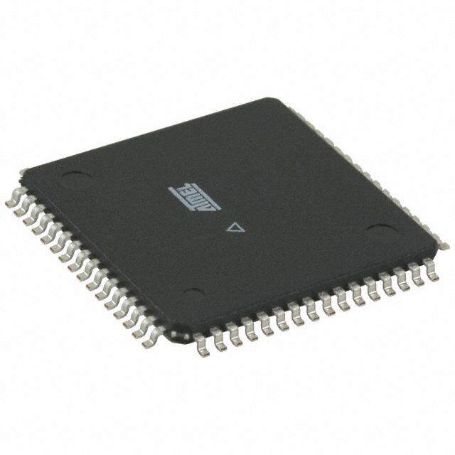
R5F100FCAFP#V0产品简介:
ICGOO电子元器件商城为您提供R5F100FCAFP#V0由RENESAS ELECTRONICS设计生产,在icgoo商城现货销售,并且可以通过原厂、代理商等渠道进行代购。 R5F100FCAFP#V0价格参考。RENESAS ELECTRONICSR5F100FCAFP#V0封装/规格:嵌入式 - 微控制器, RL78 微控制器 IC RL78/G13 16-位 32MHz 32KB(32K x 8) 闪存 44-LQFP(10x10)。您可以下载R5F100FCAFP#V0参考资料、Datasheet数据手册功能说明书,资料中有R5F100FCAFP#V0 详细功能的应用电路图电压和使用方法及教程。
Renesas Electronics America生产的R5F100FCAFP#V0是一款嵌入式微控制器,属于RL78/G13系列。该型号广泛应用于需要高效能、低功耗及高集成度的场景中,具体应用场景包括但不限于以下领域:

1. 工业控制:用于各种工业设备中的电机控制、传感器数据采集和处理等任务。其高效的计算能力和丰富的外设接口使其能够胜任复杂的工业自动化需求。

2. 家用电器:适用于洗衣机、空调、冰箱等家电产品中,负责温度控制、风扇速度调节以及用户界面管理等功能。其低功耗特性有助于提升家电的整体能效表现。

3. 消费电子:可用于便携式电子产品如电子玩具、健康监测设备(如体重秤)等领域,提供稳定可靠的运行环境并延长电池使用寿命。

4. 汽车电子:在车身控制系统中发挥作用,例如车窗升降、雨刷控制、座椅调节等方面。同时也可以作为车载信息娱乐系统的辅助处理器使用。

5. 物联网(IoT)节点:凭借其内置的安全功能和通信模块,可以成为构建智能家居或智慧城市解决方案的重要组成部分。

总之,R5F100FCAFP#V0凭借其卓越性能与灵活性,在众多需要精确控制和高效处理能力的应用场合表现出色。
| 参数 | 数值 |
| 产品目录 | 集成电路 (IC) |
| 描述 | IC MCU 16BIT 32KB FLASH 44LQFP |
| EEPROM容量 | - |
| 产品分类 | |
| I/O数 | 31 |
| 品牌 | Renesas Electronics America |
| 数据手册 | |
| 产品图片 |
|
| 产品型号 | R5F100FCAFP#V0 |
| RAM容量 | 2K x 8 |
| rohs | 无铅 / 符合限制有害物质指令(RoHS)规范要求 |
| 产品系列 | RL78/G13 |
| 产品培训模块 | http://www.digikey.cn/PTM/IndividualPTM.page?site=cn&lang=zhs&ptm=25650http://www.digikey.cn/PTM/IndividualPTM.page?site=cn&lang=zhs&ptm=25780 |
| 供应商器件封装 | 44-LQFP(10x10) |
| 其它名称 | R5F100FCAFPV0 |
| 包装 | 托盘 |
| 外设 | DMA,LVD,POR,PWM,WDT |
| 封装/外壳 | 44-LQFP |
| 工作温度 | -40°C ~ 85°C |
| 振荡器类型 | 内部 |
| 数据转换器 | A/D 10x8/10b |
| 标准包装 | 1 |
| 核心处理器 | RL78 |
| 核心尺寸 | 16-位 |
| 电压-电源(Vcc/Vdd) | 1.6 V ~ 5.5 V |
| 程序存储器类型 | 闪存 |
| 程序存储容量 | 32KB(32K x 8) |
| 连接性 | CSI, I²C, LIN, UART/USART |
| 速度 | 32MHz |


- 商务部:美国ITC正式对集成电路等产品启动337调查
- 曝三星4nm工艺存在良率问题 高通将骁龙8 Gen1或转产台积电
- 太阳诱电将投资9.5亿元在常州建新厂生产MLCC 预计2023年完工
- 英特尔发布欧洲新工厂建设计划 深化IDM 2.0 战略
- 台积电先进制程称霸业界 有大客户加持明年业绩稳了
- 达到5530亿美元!SIA预计今年全球半导体销售额将创下新高
- 英特尔拟将自动驾驶子公司Mobileye上市 估值或超500亿美元
- 三星加码芯片和SET,合并消费电子和移动部门,撤换高东真等 CEO
- 三星电子宣布重大人事变动 还合并消费电子和移动部门
- 海关总署:前11个月进口集成电路产品价值2.52万亿元 增长14.8%


PDF Datasheet 数据手册内容提取
Datasheet RL78/G13 R01DS0131EJ0340 Rev.3.40 RENESAS MCU May 31, 2018 True Low Power Platform (as low as 66 µA/MHz, and 0.57 µA for RTC + LVD), 1.6 V to 5.5 V operation, 16 to 512 Kbyte Flash, 41 DMIPS at 32 MHz, for General Purpose Applications 1. OUTLINE 1.1 Features Ultra-low power consumption technology DMA (Direct Memory Access) controller VDD = single power supply voltage of 1.6 to 5.5 V 2/4 channels HALT mode Number of clocks during transfer between 8/16-bit STOP mode SFR and internal RAM: 2 clocks SNOOZE mode Multiplier and divider/multiply-accumulator RL78 CPU core 16 bits × 16 bits = 32 bits (Unsigned or signed) CISC architecture with 3-stage pipeline 32 bits ÷ 32 bits = 32 bits (Unsigned) Minimum instruction execution time: Can be changed 16 bits × 16 bits + 32 bits = 32 bits (Unsigned or from high speed (0.03125 μs: @ 32 MHz operation signed) with high-speed on-chip oscillator) to ultra-low speed Serial interface (30.5 μs: @ 32.768 kHz operation with subsystem CSI: 2 to 8 channels clock) UART/UART (LIN-bus supported): 2 to 4 channels Address space: 1 MB I2C/Simplified I2C communication: 2 to 8 channels General-purpose registers: (8-bit register × 8) × 4 banks Timer On-chip RAM: 2 to 32 KB 16-bit timer: 8 to 16 channels 12-bit interval timer: 1 channel Code flash memory Real-time clock: 1 channel (calendar for 99 years, Code flash memory: 16 to 512 KB alarm function, and clock Block size: 1 KB correction function) Prohibition of block erase and rewriting (security Watchdog timer: 1 channel (operable with the function) dedicated low-speed on-chip On-chip debug function oscillator) Self-programming (with boot swap function/flash shield window function) A/D converter Data Flash Memory 8/10-bit resolution A/D converter (VDD = 1.6 to 5.5 V) Analog input: 6 to 26 channels Data flash memory: 4 KB to 8 KB Internal reference voltage (1.45 V) and temperature Back ground operation (BGO): Instructions can be sensor Note 1 executed from the program memory while rewriting the data flash memory. I/O port Number of rewrites: 1,000,000 times (TYP.) I/O port: 16 to 120 (N-ch open drain I/O [withstand Voltage of rewrites: VDD = 1.8 to 5.5 V voltage of 6 V]: 0 to 4, N-ch open drain I/O [VDD withstand voltage Note 2/EVDD withstand High-speed on-chip oscillator voltage Note 3]: 5 to 25) Select from 32 MHz, 24 MHz, 16 MHz, 12 MHz, 8 MHz, Can be set to N-ch open drain, TTL input buffer, and 6 MHz, 4 MHz, 3 MHz, 2 MHz, and 1 MHz on-chip pull-up resistor High accuracy: +/- 1.0 % (VDD = 1.8 to 5.5 V, TA = -20 Different potential interface: Can connect to a 1.8/2.5/3 to +85°C) V device Operating ambient temperature On-chip key interrupt function TA = -40 to +85°C (A: Consumer applications, D: On-chip clock output/buzzer output controller Industrial applications ) Others TA = -40 to +105°C (G: Industrial applications) On-chip BCD (binary-coded decimal) correction circuit Power management and reset function On-chip power-on-reset (POR) circuit Notes 1. Can be selected only in HS (high-speed main) mode On-chip voltage detector (LVD) (Select interrupt and 2. Products with 20 to 52 pins reset from 14 levels) 3. Products with 64 to 128 pins Remark The functions mounted depend on the product. See 1.6 Outline of Functions. R01DS0131EJ0340 Rev.3.40 1 of 194 May 31, 2018
RL78/G13 1. OUTLINE Ο ROM, RAM capacities Flash Data RAM RL78/G13 ROM flash 20 pins 24 pins 25 pins 30 pins 32 pins 36 pins 128 8 KB 12 – – – R5F100AG R5F100BG R5F100CG KB – KB – – – R5F101AG R5F101BG R5F101CG 96 8 KB 8 KB – – – R5F100AF R5F100BF R5F100CF KB – – – – R5F101AF R5F101BF R5F101CF 64 4 KB 4 KB R5F1006E R5F1007E R5F1008E R5F100AE R5F100BE R5F100CE KB – Note R5F1016E R5F1017E R5F1018E R5F101AE R5F101BE R5F101CE 48 4 KB 3 KB R5F1006D R5F1007D R5F1008D R5F100AD R5F100BD R5F100CD KB Note – R5F1016D R5F1017D R5F1018D R5F101AD R5F101BD R5F101CD 32 4 KB 2 KB R5F1006C R5F1007C R5F1008C R5F100AC R5F100BC R5F100CC KB – R5F1016C R5F1017C R5F1018C R5F101AC R5F101BC R5F101CC 16 4 KB 2 KB R5F1006A R5F1007A R5F1008A R5F100AA R5F100BA R5F100CA KB – R5F1016A R5F1017A R5F1018A R5F101AA R5F101BA R5F101CA Flash Data RAM RL78/G13 ROM flash 40 pins 44 pins 48 pins 52 pins 64 pins 80 pins 100 pins 128 pins 512 8 KB 32 KB – R5F100FL R5F100GL R5F100JL R5F100LL R5F100ML R5F100PL R5F100SL KB Note – – R5F101FL R5F101GL R5F101JL R5F101LL R5F101ML R5F101PL R5F101SL 384 8 KB 24 KB – R5F100FK R5F100GK R5F100JK R5F100LK R5F100MK R5F100PK R5F100SK KB – – R5F101FK R5F101GK R5F101JK R5F101LK R5F101MK R5F101PK R5F101SK 256 8 KB 20 KB – R5F100FJ R5F100GJ R5F100JJ R5F100LJ R5F100MJ R5F100PJ R5F100SJ KB Note – – R5F101FJ R5F101GJ R5F101JJ R5F101LJ R5F101MJ R5F101PJ R5F101SJ 192 8 KB 16 KB R5F100EH R5F100FH R5F100GH R5F100JH R5F100LH R5F100MH R5F100PH R5F100SH KB – R5F101EH R5F101FH R5F101GH R5F101JH R5F101LH R5F101MH R5F101PH R5F101SH 128 8 KB 12 KB R5F100EG R5F100FG R5F100GG R5F100JG R5F100LG R5F100MG R5F100PG – KB – R5F101EG R5F101FG R5F101GG R5F101JG R5F101LG R5F101MG R5F101PG – 96 8 KB 8 KB R5F100EF R5F100FF R5F100GF R5F100JF R5F100LF R5F100MF R5F100PF – KB – R5F101EF R5F101FF R5F101GF R5F101JF R5F101LF R5F101MF R5F101PF – 64 4 KB 4 KB R5F100EE R5F100FE R5F100GE R5F100JE R5F100LE – – – KB Note – R5F101EE R5F101FE R5F101GE R5F101JE R5F101LE – – – 48 4 KB 3 KB R5F100ED R5F100FD R5F100GD R5F100JD R5F100LD – – – KB Note – R5F101ED R5F101FD R5F101GD R5F101JD R5F101LD – – – 32 4 KB 2 KB R5F100EC R5F100FC R5F100GC R5F100JC R5F100LC – – – KB – R5F101EC R5F101FC R5F101GC R5F101JC R5F101LC – – – 16 4 KB 2 KB R5F100EA R5F100FA R5F100GA – – – – – KB – R5F101EA R5F101FA R5F101GA – – – – – Note The flash library uses RAM in self-programming and rewriting of the data flash memory. The target products and start address of the RAM areas used by the flash library are shown below. R5F100xD, R5F101xD (x = 6 to 8, A to C, E to G, J, L): Start address FF300H R5F100xE, R5F101xE (x = 6 to 8, A to C, E to G, J, L): Start address FEF00H R5F100xJ, R5F101xJ (x = F, G, J, L, M, P): Start address FAF00H R5F100xL, R5F101xL (x = F, G, J, L, M, P, S): Start address F7F00H For the RAM areas used by the flash library, see Self RAM list of Flash Self-Programming Library for RL78 Family (R20UT2944). R01DS0131EJ0340 Rev.3.40 2 of 194 May 31, 2018
RL78/G13 1. OUTLINE 1.2 List of Part Numbers Figure 1-1. Part Number, Memory Size, and Package of RL78/G13 Part No. R 5 F 1 0 0 L E A x x x F B #V0 Packaging specification #U0 : Tray (HWQFN,VFBGA,WFLGA) #V0 : Tray (LFQFP,LQFP,LSSOP) #W0 : Embossed Tape (HWQFN,VFBGA,WFLGA) #X0 : Embossed Tape (LFQFP,LQFP,LSSOP) Package type: SP : LSSOP, 0.65 mm pitch FP : LFQFP, 0.80 mm pitch FA : LFQFP, 0.65 mm pitch FB : LFQFP, 0.50 mm pitch NA : HWQFN, 0.50 mm pitch LA : WFLGA, 0.50 mm pitchNote1 BG : VFBGA, 0.40 mm pitchNote1 ROM number (Omitted with blank products) Fields of application: A : Consumer applications, operating ambient temperature : -40°C to +85°C D : Industrial applications, operating ambient temperature : -40°C to +85°C G : Industrial applications, operating ambient temperature : -40°C to +105°C ROM capacity: A : 16 KB C : 32 KB D : 48 KB E : 64 KB F : 96 KB G : 128 KB H : 192 KB J : 256 KB K : 384 KBNote2 L : 512 KBNote2 Pin count: 6 : 20-pin 7 : 24-pin 8 : 25-pinNote1 A : 30-pin B : 32-pin C : 36-pinNote1 E : 40-pin F : 44-pin G : 48-pin J : 52-pin L : 64-pin M : 80-pin P : 100-pin S : 128-pinNote2 RL78/G13 group 100 : Data flash is provided 101 : Data flash is not providedNote2 Memory type: F : Flash memory Renesas MCU Renesas semiconductor product Notes 1. Products only for “A: Consumer applications (TA = –40 to +85°C)”, and "G: Industrial applications (TA = –40 to +105°C)" 2. Products only for “A: Consumer applications (TA = –40 to +85°C)”, and "D: Industrial applications (TA = –40 to +85°C)" R01DS0131EJ0340 Rev.3.40 3 of 194 May 31, 2018
RL78/G13 1. OUTLINE Table 1-1. List of Ordering Part Numbers (1/12) Pin Package Data Fields of Ordering Part Number count flash Application Note 20 pins 20-pin plastic LSSOP Mounted A R5F1006AASP#V0, R5F1006CASP#V0, R5F1006DASP#V0, (7.62 mm (300), 0.65 R5F1006EASP#V0 mm pitch) R5F1006AASP#X0, R5F1006CASP#X0, R5F1006DASP#X0, R5F1006EASP#X0 D R5F1006ADSP#V0, R5F1006CDSP#V0, R5F1006DDSP#V0, R5F1006EDSP#V0 R5F1006ADSP#X0, R5F1006CDSP#X0, R5F1006DDSP#X0, R5F1006EDSP#X0 G R5F1006AGSP#V0, R5F1006CGSP#V0, R5F1006DGSP#V0, R5F1006EGSP#V0 R5F1006AGSP#X0, R5F1006CGSP#X0, R5F1006DGSP#X0, R5F1006EGSP#X0 Not A R5F1016AASP#V0, R5F1016CASP#V0, R5F1016DASP#V0, mounted R5F1016EASP#V0 R5F1016AASP#X0, R5F1016CASP#X0, R5F1016DASP#X0, R5F1016EASP#X0 D R5F1016ADSP#V0, R5F1016CDSP#V0, R5F1016DDSP#V0, R5F1016EDSP#V0 R5F1016ADSP#X0, R5F1016CDSP#X0, R5F1016DDSP#X0, R5F1016EDSP#X0 24 pins 24-pin plastic HWQFN Mounted A R5F1007AANA#U0, R5F1007CANA#U0, R5F1007DANA#U0, (4 × 4mm, 0.5 mm R5F1007EANA#U0 pitch) R5F1007AANA#W0, R5F1007CANA#W0, R5F1007DANA#W0, R5F1007EANA#W0 D R5F1007ADNA#U0, R5F1007CDNA#U0, R5F1007DDNA#U0, R5F1007EDNA#U0 R5F1007ADNA#W0, R5F1007CDNA#W0, R5F1007DDNA#W0, R5F1007EDNA#W0 G R5F1007AGNA#U0, R5F1007CGNA#U0, R5F1007DGNA#U0, R5F1007EGNA#U0 R5F1007AGNA#W0, R5F1007CGNA#W0, R5F1007DGNA#W0, R5F1007EGNA#W0 Not A R5F1017AANA#U0, R5F1017CANA#U0, R5F1017DANA#U0, mounted R5F1017EANA#U0 R5F1017AANA#W0, R5F1017CANA#W0, R5F1017DANA#W0, R5F1017EANA#W0 D R5F1017ADNA#U0, R5F1017CDNA#U0, R5F1017DDNA#U0, R5F1017EDNA#U0 R5F1017ADNA#W0, R5F1017CDNA#W0, R5F1017DDNA#W0, R5F1017EDNA#W0 Note For the fields of application, refer to Figure 1-1 Part Number, Memory Size, and Package of RL78/G13. Caution The ordering part numbers represent the numbers at the time of publication. For the latest ordering part numbers, refer to the target product page of the Renesas Electronics website. R01DS0131EJ0340 Rev.3.40 4 of 194 May 31, 2018
RL78/G13 1. OUTLINE Table 1-1. List of Ordering Part Numbers (2/12) Pin Package Data Fields of Ordering Part Number count flash Application Note 25 pins 25-pin plastic WFLGA Mounted A R5F1008AALA#U0, R5F1008CALA#U0, R5F1008DALA#U0, (3 × 3 mm, 0.5 mm R5F1008EALA#U0 R5F1008AALA#W0, R5F1008CALA#W0, R5F1008DALA#W0, pitch) R5F1008EALA#W0 G R5F1008AGLA#U0, R5F1008CGLA#U0, R5F1008DGLA#U0, R5F1008EGLA#U0 R5F1008AGLA#W0, R5F1008CGLA#W0, R5F1008DGLA#W0, R5F1008EGLA#W0 Not A R5F1018AALA#U0, R5F1018CALA#U0, R5F1018DALA#U0, R5F1018EALA#U0 mounted R5F1018AALA#W0, R5F1018CALA#W0, R5F1018DALA#W0, R5F1018EALA#W0 30 pins 30-pin plastic LSSOP Mounted A R5F100AAASP#V0, R5F100ACASP#V0, R5F100ADASP#V0, R5F100AEASP#V0, R5F100AFASP#V0, R5F100AGASP#V0 (7.62 mm (300), 0.65 R5F100AAASP#X0, R5F100ACASP#X0, R5F100ADASP#X0 mm pitch) R5F100AEASP#X0, R5F100AFASP#X0, R5F100AGASP#X0 D R5F100AADSP#V0, R5F100ACDSP#V0, R5F100ADDSP#V0, R5F100AEDSP#V0, R5F100AFDSP#V0, R5F100AGDSP#V0 R5F100AADSP#X0, R5F100ACDSP#X0, R5F100ADDSP#X0, R5F100AEDSP#X0, R5F100AFDSP#X0, R5F100AGDSP#X0 G R5F100AAGSP#V0, R5F100ACGSP#V0, R5F100ADGSP#V0,R5F100AEGSP#V0, R5F100AFGSP#V0, R5F100AGGSP#V0 R5F100AAGSP#X0, R5F100ACGSP#X0, R5F100ADGSP#X0,R5F100AEGSP#X0, R5F100AFGSP#X0, R5F100AGGSP#X0 Not A R5F101AAASP#V0, R5F101ACASP#V0, R5F101ADASP#V0, R5F101AEASP#V0, R5F101AFASP#V0, R5F101AGASP#V0 mounted R5F101AAASP#X0, R5F101ACASP#X0, R5F101ADASP#X0, R5F101AEASP#X0, R5F101AFASP#X0, R5F101AGASP#X0 D R5F101AADSP#V0, R5F101ACDSP#V0, R5F101ADDSP#V0, R5F101AEDSP#V0, R5F101AFDSP#V0, R5F101AGDSP#V0 R5F101AADSP#X0, R5F101ACDSP#X0, R5F101ADDSP#X0, R5F101AEDSP#X0, R5F101AFDSP#X0, R5F101AGDSP#X0 32 pins 32-pin plastic HWQFN Mounted A R5F100BAANA#U0, R5F100BCANA#U0, R5F100BDANA#U0, (5 × 5 mm, 0.5 mm R5F100BEANA#U0, R5F100BFANA#U0, R5F100BGANA#U0 R5F100BAANA#W0, R5F100BCANA#W0, R5F100BDANA#W0, pitch) R5F100BEANA#W0, R5F100BFANA#W0, R5F100BGANA#W0 D R5F100BADNA#U0, R5F100BCDNA#U0, R5F100BDDNA#U0, R5F100BEDNA#U0, R5F100BFDNA#U0, R5F100BGDNA#U0 R5F100BADNA#W0, R5F100BCDNA#W0, R5F100BDDNA#W0, R5F100BEDNA#W0, R5F100BFDNA#W0, R5F100BGDNA#W0 G R5F100BAGNA#U0, R5F100BCGNA#U0, R5F100BDGNA#U0, R5F100BEGNA#U0, R5F100BFGNA#U0, R5F100BGGNA#U0 R5F100BAGNA#W0, R5F100BCGNA#W0, R5F100BDGNA#W0, R5F100BEGNA#W0, R5F100BFGNA#W0, R5F100BGGNA#W0 Not A R5F101BAANA#U0, R5F101BCANA#U0, R5F101BDANA#U0, R5F101BEANA#U0, R5F101BFANA#U0, R5F101BGANA#U0 mounted R5F101BAANA#W0, R5F101BCANA#W0, R5F101BDANA#W0, R5F101BEANA#W0, R5F101BFANA#W0, R5F101BGANA#W0 D R5F101BADNA#U0, R5F101BCDNA#U0, R5F101BDDNA#U0, R5F101BEDNA#U0, R5F101BFDNA#U0, R5F101BGDNA#U0 R5F101BADNA#W0, R5F101BCDNA#W0, R5F101BDDNA#W0, R5F101BEDNA#W0, R5F101BFDNA#W0, R5F101BGDNA#W0 Note For the fields of application, refer to Figure 1-1 Part Number, Memory Size, and Package of RL78/G13. Caution The ordering part numbers represent the numbers at the time of publication. For the latest ordering part numbers, refer to the target product page of the Renesas Electronics website. R01DS0131EJ0340 Rev.3.40 5 of 194 May 31, 2018
RL78/G13 1. OUTLINE Table 1-1. List of Ordering Part Numbers (3/12) Pin Package Data flash Fields of Ordering Part Number count Application Note 36 pins 36-pin plastic WFLGA Mounted A R5F100CAALA#U0, R5F100CCALA#U0, R5F100CDALA#U0, (4 × 4 mm, 0.5 mm pitch) R5F100CEALA#U0, R5F100CFALA#U0, R5F100CGALA#U0 R5F100CAALA#W0, R5F100CCALA#W0, R5F100CDALA#W0, R5F100CEALA#W0, R5F100CFALA#W0, R5F100CGALA#W0 G R5F100CAGLA#U0, R5F100CCGLA#U0, R5F100CDGLA#U0, R5F100CEGLA#U0, R5F100CFGLA#U0, R5F100CGGLA#U0 R5F100CAGLA#W0, R5F100CCGLA#W0, R5F100CDGLA#W0, R5F100CEGLA#W0, R5F100CFGLA#W0, R5F100CGGLA#W0 Not A R5F101CAALA#U0, R5F101CCALA#U0, R5F101CDALA#U0, mounted R5F101CEALA#U0, R5F101CFALA#U0, R5F101CGALA#U0 R5F101CAALA#W0, R5F101CCALA#W0, R5F101CDALA#W0, R5F101CEALA#W0, R5F101CFALA#W0, R5F101CGALA#W0 40 pins 40-pin plastic HWQFN Mounted A R5F100EAANA#U0, R5F100ECANA#U0, R5F100EDANA#U0, (6 × 6 mm, 0.5 mm pitch) R5F100EEANA#U0, R5F100EFANA#U0, R5F100EGANA#U0, R5F100EHANA#U0 R5F100EAANA#W0, R5F100ECANA#W0, R5F100EDANA#W0, R5F100EEANA#W0, R5F100EFANA#W0, R5F100EGANA#W0, R5F100EHANA#W0 D R5F100EADNA#U0, R5F100ECDNA#U0, R5F100EDDNA#U0, R5F100EEDNA#U0, R5F100EFDNA#U0, R5F100EGDNA#U0, R5F100EHDNA#U0 R5F100EADNA#W0, R5F100ECDNA#W0, R5F100EDDNA#W0, R5F100EEDNA#W0, R5F100EFDNA#W0, R5F100EGDNA#W0, R5F100EHDNA#W0 G R5F100EAGNA#U0, R5F100ECGNA#U0, R5F100EDGNA#U0, R5F100EEGNA#U0, R5F100EFGNA#U0, R5F100EGGNA#U0, R5F100EHGNA#U0 R5F100EAGNA#W0, R5F100ECGNA#W0, R5F100EDGNA#W0, R5F100EEGNA#W0, R5F100EFGNA#W0, R5F100EGGNA#W0, R5F100EHGNA#W0 Not A R5F101EAANA#U0, R5F101ECANA#U0, R5F101EDANA#U0, mounted R5F101EEANA#U0, R5F101EFANA#U0, R5F101EGANA#U0, R5F101EHANA#U0 R5F101EAANA#W0, R5F101ECANA#W0, R5F101EDANA#W0, R5F101EEANA#W0, R5F101EFANA#W0, R5F101EGANA#W0, R5F101EHANA#W0 D R5F101EADNA#U0, R5F101ECDNA#U0, R5F101EDDNA#U0, R5F101EEDNA#U0, R5F101EFDNA#U0, R5F101EGDNA#U0, R5F101EHDNA#U0 R5F101EADNA#W0, R5F101ECDNA#W0, R5F101EDDNA#W0, R5F101EEDNA#W0, R5F101EFDNA#W0, R5F101EGDNA#W0, R5F101EHDNA#W0 Note For the fields of application, refer to Figure 1-1 Part Number, Memory Size, and Package of RL78/G13. Caution The ordering part numbers represent the numbers at the time of publication. For the latest ordering part numbers, refer to the target product page of the Renesas Electronics website. R01DS0131EJ0340 Rev.3.40 6 of 194 May 31, 2018
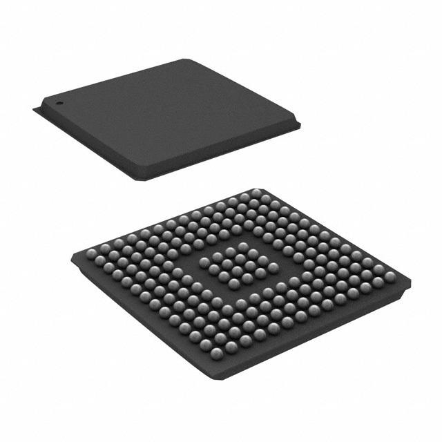
RL78/G13 1. OUTLINE Table 1-1. List of Ordering Part Numbers (4/12) Pin Package Data flash Fields of Ordering Part Number count Application Note 44 pins 44-pin plastic LQFP Mounted A R5F100FAAFP#V0, R5F100FCAFP#V0, R5F100FDAFP#V0, (10 × 10 mm, 0.8 mm R5F100FEAFP#V0, R5F100FFAFP#V0, R5F100FGAFP#V0, pitch) R5F100FHAFP#V0, R5F100FJAFP#V0, R5F100FKAFP#V0, R5F100FLAFP#V0 R5F100FAAFP#X0, R5F100FCAFP#X0, R5F100FDAFP#X0, R5F100FEAFP#X0, R5F100FFAFP#X0, R5F100FGAFP#X0, R5F100FHAFP#X0, R5F100FJAFP#X0, R5F100FKAFP#X0, R5F100FLAFP#X0 D R5F100FADFP#V0, R5F100FCDFP#V0, R5F100FDDFP#V0, R5F100FEDFP#V0, R5F100FFDFP#V0, R5F100FGDFP#V0, R5F100FHDFP#V0, R5F100FJDFP#V0, R5F100FKDFP#V0, R5F100FLDFP#V0 R5F100FADFP#X0, R5F100FCDFP#X0, R5F100FDDFP#X0, R5F100FEDFP#X0, R5F100FFDFP#X0, R5F100FGDFP#X0, R5F100FHDFP#X0, R5F100FJDFP#X0, R5F100FKDFP#X0, R5F100FLDFP#X0 G R5F100FAGFP#V0, R5F100FCGFP#V0, R5F100FDGFP#V0, R5F100FEGFP#V0, R5F100FFGFP#V0, R5F100FGGFP#V0, R5F100FHGFP#V0, R5F100FJGFP#V0 R5F100FAGFP#X0, R5F100FCGFP#X0, R5F100FDGFP#X0, R5F100FEGFP#X0, R5F100FFGFP#X0, R5F100FGGFP#X0, R5F100FHGFP#X0, R5F100FJGFP#X0 Not A R5F101FAAFP#V0, R5F101FCAFP#V0, R5F101FDAFP#V0, mounted R5F101FEAFP#V0, R5F101FFAFP#V0, R5F101FGAFP#V0, R5F101FHAFP#V0, R5F101FJAFP#V0, R5F101FKAFP#V0, R5F101FLAFP#V0 R5F101FAAFP#X0, R5F101FCAFP#X0, R5F101FDAFP#X0, R5F101FEAFP#X0, R5F101FFAFP#X0, R5F101FGAFP#X0, R5F101FHAFP#X0, R5F101FJAFP#X0, R5F101FKAFP#X0, R5F101FLAFP#X0 D R5F101FADFP#V0, R5F101FCDFP#V0, R5F101FDDFP#V0, R5F101FEDFP#V0, R5F101FFDFP#V0, R5F101FGDFP#V0, R5F101FHDFP#V0, R5F101FJDFP#V0, R5F101FKDFP#V0, R5F101FLDFP#V0 R5F101FADFP#X0, R5F101FCDFP#X0, R5F101FDDFP#X0, R5F101FEDFP#X0, R5F101FFDFP#X0, R5F101FGDFP#X0, R5F101FHDFP#X0, R5F101FJDFP#X0, R5F101FKDFP#X0, R5F101FLDFP#X0 Note For the fields of application, refer to Figure 1-1 Part Number, Memory Size, and Package of RL78/G13. Caution The ordering part numbers represent the numbers at the time of publication. For the latest ordering part numbers, refer to the target product page of the Renesas Electronics website. R01DS0131EJ0340 Rev.3.40 7 of 194 May 31, 2018
RL78/G13 1. OUTLINE Table 1-1. List of Ordering Part Numbers (5/12) Pin count Package Data flash Fields of Ordering Part Number Application Note 48 pins 48-pin plastic LFQFP Mounted A R5F100GAAFB#V0, R5F100GCAFB#V0, R5F100GDAFB#V0, (7 × 7 mm, 0.5 mm R5F100GEAFB#V0, R5F100GFAFB#V0, R5F100GGAFB#V0, pitch) R5F100GHAFB#V0, R5F100GJAFB#V0, R5F100GKAFB#V0, R5F100GLAFB#V0 R5F100GAAFB#X0, R5F100GCAFB#X0, R5F100GDAFB#X0, R5F100GEAFB#X0, R5F100GFAFB#X0, R5F100GGAFB#X0, R5F100GHAFB#X0, R5F100GJAFB#X0, R5F100GKAFB#X0, R5F100GLAFB#X0 D R5F100GADFB#V0, R5F100GCDFB#V0, R5F100GDDFB#V0, R5F100GEDFB#V0, R5F100GFDFB#V0, R5F100GGDFB#V0, R5F100GHDFB#V0, R5F100GJDFB#V0, R5F100GKDFB#V0, R5F100GLDFB#V0 R5F100GADFB#X0, R5F100GCDFB#X0, R5F100GDDFB#X0, R5F100GEDFB#X0, R5F100GFDFB#X0, R5F100GGDFB#X0, R5F100GHDFB#X0, R5F100GJDFB#X0, R5F100GKDFB#X0, R5F100GLDFB#X0 G R5F100GAGFB#V0, R5F100GCGFB#V0, R5F100GDGFB#V0, R5F100GEGFB#V0, R5F100GFGFB#V0, R5F100GGGFB#V0, R5F100GHGFB#V0, R5F100GJGFB#V0 R5F100GAGFB#X0, R5F100GCGFB#X0, R5F100GDGFB#X0, R5F100GEGFB#X0, R5F100GFGFB#X0, R5F100GGGFB#X0, R5F100GHGFB#X0, R5F100GJGFB#X0 Not A R5F101GAAFB#V0, R5F101GCAFB#V0, R5F101GDAFB#V0, mounted R5F101GEAFB#V0, R5F101GFAFB#V0, R5F101GGAFB#V0, R5F101GHAFB#V0, R5F101GJAFB#V0, R5F101GKAFB#V0, R5F101GLAFB#V0 R5F101GAAFB#X0, R5F101GCAFB#X0, R5F101GDAFB#X0, R5F101GEAFB#X0, R5F101GFAFB#X0, R5F101GGAFB#X0, R5F101GHAFB#X0, R5F101GJAFB#X0, R5F101GKAFB#X0, R5F101GLAFB#X0 D R5F101GADFB#V0, R5F101GCDFB#V0, R5F101GDDFB#V0, R5F101GEDFB#V0, R5F101GFDFB#V0, R5F101GGDFB#V0, R5F101GHDFB#V0, R5F101GJDFB#V0, R5F101GKDFB#V0, R5F101GLDFB#V0 R5F101GADFB#X0, R5F101GCDFB#X0, R5F101GDDFB#X0, R5F101GEDFB#X0, R5F101GFDFB#X0, R5F101GGDFB#X0, R5F101GHDFB#X0, R5F101GJDFB#X0, R5F101GKDFB#X0, R5F101GLDFB#X0 Note For the fields of application, refer to Figure 1-1 Part Number, Memory Size, and Package of RL78/G13. Caution The ordering part numbers represent the numbers at the time of publication. For the latest ordering part numbers, refer to the target product page of the Renesas Electronics website. R01DS0131EJ0340 Rev.3.40 8 of 194 May 31, 2018
RL78/G13 1. OUTLINE Table 1-1. List of Ordering Part Numbers (6/12) Pin count Package Data flash Fields of Ordering Part Number Application Note 48 pins 48-pin plastic HWQFN Mounted A R5F100GAANA#U0, R5F100GCANA#U0, R5F100GDANA#U0, (7 × 7 mm, 0.5 mm R5F100GEANA#U0, R5F100GFANA#U0, R5F100GGANA#U0, pitch) R5F100GHANA#U0, R5F100GJANA#U0, R5F100GKANA#U0, R5F100GLANA#U0 R5F100GAANA#W0, R5F100GCANA#W0, R5F100GDANA#W0, R5F100GEANA#W0, R5F100GFANA#W0, R5F100GGANA#W0, R5F100GHANA#W0, R5F100GJANA#W0, R5F100GKANA#W0, R5F100GLANA#W0 D R5F100GADNA#U0, R5F100GCDNA#U0, R5F100GDDNA#U0, R5F100GEDNA#U0, R5F100GFDNA#U0, R5F100GGDNA#U0, R5F100GHDNA#U0, R5F100GJDNA#U0, R5F100GKDNA#U0, R5F100GLDNA#U0 R5F100GADNA#W0, R5F100GCDNA#W0, R5F100GDDNA#W0, R5F100GEDNA#W0, R5F100GFDNA#W0, R5F100GGDNA#W0, R5F100GHDNA#W0, R5F100GJDNA#W0, R5F100GKDNA#W0, R5F100GLDNA#W0 G R5F100GAGNA#U0, R5F100GCGNA#U0, R5F100GDGNA#U0, R5F100GEGNA#U0, R5F100GFGNA#U0, R5F100GGGNA#U0, R5F100GHGNA#U0, R5F100GJGNA#U0 R5F100GAGNA#W0, R5F100GCGNA#W0, R5F100GDGNA#W0, R5F100GEGNA#W0, R5F100GFGNA#W0, R5F100GGGNA#W0, R5F100GHGNA#W0, R5F100GJGNA#W0 Not A R5F101GAANA#U0, R5F101GCANA#U0, R5F101GDANA#U0, mounted R5F101GEANA#U0, R5F101GFANA#U0, R5F101GGANA#U0, R5F101GHANA#U0, R5F101GJANA#U0, R5F101GKANA#U0, R5F101GLANA#U0 R5F101GAANA#W0, R5F101GCANA#W0, R5F101GDANA#W0, R5F101GEANA#W0, R5F101GFANA#W0, R5F101GGANA#W0, R5F101GHANA#W0, R5F101GJANA#W0, R5F101GKANA#W0, R5F101GLANA#W0 D R5F101GADNA#U0, R5F101GCDNA#U0, R5F101GDDNA#U0, R5F101GEDNA#U0, R5F101GFDNA#U0, R5F101GGDNA#U0, R5F101GHDNA#U0, R5F101GJDNA#U0, R5F101GKDNA#U0, R5F101GLDNA#U0 R5F101GADNA#W0, R5F101GCDNA#W0, R5F101GDDNA#W0, R5F101GEDNA#W0, R5F101GFDNA#W0, R5F101GGDNA#W0, R5F101GHDNA#W0, R5F101GJDNA#W0, R5F101GKDNA#W0, R5F101GLDNA#W0 Note For the fields of application, refer to Figure 1-1 Part Number, Memory Size, and Package of RL78/G13. Caution The ordering part numbers represent the numbers at the time of publication. For the latest ordering part numbers, refer to the target product page of the Renesas Electronics website. R01DS0131EJ0340 Rev.3.40 9 of 194 May 31, 2018
RL78/G13 1. OUTLINE Table 1-1. List of Ordering Part Numbers (7/12) Pin count Package Data flash Fields of Ordering Part Number Application Note 52 pins 52-pin plastic LQFP Mounted A R5F100JCAFA#V0, R5F100JDAFA#V0, R5F100JEAFA#V0, (10 × 10 mm, 0.65 R5F100JFAFA#V0, R5F100JGAFA#V0, R5F100JHAFA#V0, mm pitch) R5F100JJAFA#V0, R5F100JKAFA#V0, R5F100JLAFA#V0 R5F100JCAFA#X0, R5F100JDAFA#X0, R5F100JEAFA#X0, R5F100JFAFA#X0, R5F100JGAFA#X0, R5F100JHAFA#X0, R5F100JJAFA#X0, R5F100JKAFA#X0, R5F100JLAFA#X0 D R5F100JCDFA#V0, R5F100JDDFA#V0, R5F100JEDFA#V0, R5F100JFDFA#V0, R5F100JGDFA#V0, R5F100JHDFA#V0, R5F100JJDFA#V0, R5F100JKDFA#V0, R5F100JLDFA#V0 R5F100JCDFA#X0, R5F100JDDFA#X0, R5F100JEDFA#X0, R5F100JFDFA#X0, R5F100JGDFA#X0, R5F100JHDFA#X0, R5F100JJDFA#X0, R5F100JKDFA#X0, R5F100JLDFA#X0 G R5F100JCGFA#V0, R5F100JDGFA#V0, R5F100JEGFA#V0, R5F100JFGFA#V0,R5F100JGGFA#V0, R5F100JHGFA#V0, R5F100JJGFA#V0 R5F100JCGFA#X0, R5F100JDGFA#X0, R5F100JEGFA#X0, R5F100JFGFA#X0,R5F100JGGFA#X0, R5F100JHGFA#X0, R5F100JJGFA#X0 Not A R5F101JCAFA#V0, R5F101JDAFA#V0, R5F101JEAFA#V0, mounted R5F101JFAFA#V0, R5F101JGAFA#V0, R5F101JHAFA#V0, R5F101JJAFA#V0, R5F101JKAFA#V0, R5F101JLAFA#V0 R5F101JCAFA#X0, R5F101JDAFA#X0, R5F101JEAFA#X0, R5F101JFAFA#X0, R5F101JGAFA#X0, R5F101JHAFA#X0, R5F101JJAFA#X0, R5F101JKAFA#X0, R5F101JLAFA#X0 D R5F101JCDFA#V0, R5F101JDDFA#V0, R5F101JEDFA#V0, R5F101JFDFA#V0, R5F101JGDFA#V0, R5F101JHDFA#V0, R5F101JJDFA#V0, R5F101JKDFA#V0, R5F101JLDFA#V0 R5F101JCDFA#X0, R5F101JDDFA#X0, R5F101JEDFA#X0, R5F101JFDFA#X0, R5F101JGDFA#X0, R5F101JHDFA#X0, R5F101JJDFA#X0, R5F101JKDFA#X0, R5F101JLDFA#X0 Note For the fields of application, refer to Figure 1-1 Part Number, Memory Size, and Package of RL78/G13. Caution The ordering part numbers represent the numbers at the time of publication. For the latest ordering part numbers, refer to the target product page of the Renesas Electronics website. R01DS0131EJ0340 Rev.3.40 10 of 194 May 31, 2018
RL78/G13 1. OUTLINE Table 1-1. List of Ordering Part Numbers (8/12) Pin count Package Data flash Fields of Ordering Part Number Application Note 64 pins 64-pin plastic LQFP Mounted A R5F100LCAFA#V0, R5F100LDAFA#V0, R5F100LEAFA#V0, (12 × 12 mm, 0.65 mm R5F100LFAFA#V0, R5F100LGAFA#V0, R5F100LHAFA#V0, pitch) R5F100LJAFA#V0, R5F100LKAFA#V0, R5F100LLAFA#V0 R5F100LCAFA#X0, R5F100LDAFA#X0, R5F100LEAFA#X0, R5F100LFAFA#X0, R5F100LGAFA#X0, R5F100LHAFA#X0, R5F100LJAFA#X0, R5F100LKAFA#X0, R5F100LLAFA#X0 D R5F100LCDFA#V0, R5F100LDDFA#V0, R5F100LEDFA#V0, R5F100LFDFA#V0, R5F100LGDFA#V0, R5F100LHDFA#V0, R5F100LJDFA#V0, R5F100LKDFA#V0, R5F100LLDFA#V0 R5F100LCDFA#X0, R5F100LDDFA#X0, R5F100LEDFA#X0, R5F100LFDFA#X0, R5F100LGDFA#X0, R5F100LHDFA#X0, R5F100LJDFA#X0, R5F100LKDFA#X0, R5F100LLDFA#X0 G R5F100LCGFA#V0, R5F100LDGFA#V0, R5F100LEGFA#V0, R5F100LFGFA#V0 R5F100LCGFA#X0, R5F100LDGFA#X0, R5F100LEGFA#X0, R5F100LFGFA#X0 R5F100LGGFA#V0, R5F100LHGFA#V0, R5F100LJGFA#V0 R5F100LGGFA#X0, R5F100LHGFA#X0, R5F100LJGFA#X0 Not A R5F101LCAFA#V0, R5F101LDAFA#V0, R5F101LEAFA#V0, mounted R5F101LFAFA#V0, R5F101LGAFA#V0, R5F101LHAFA#V0, R5F101LJAFA#V0, R5F101LKAFA#V0, R5F101LLAFA#V0 R5F101LCAFA#X0, R5F101LDAFA#X0, R5F101LEAFA#X0, R5F101LFAFA#X0, R5F101LGAFA#X0, R5F101LHAFA#X0, R5F101LJAFA#X0, R5F101LKAFA#X0, R5F101LLAFA#X0 D R5F101LCDFA#V0, R5F101LDDFA#V0, R5F101LEDFA#V0, R5F101LFDFA#V0, R5F101LGDFA#V0, R5F101LHDFA#V0, R5F101LJDFA#V0, R5F101LKDFA#V0, R5F101LLDFA#V0 R5F101LCDFA#X0, R5F101LDDFA#X0, R5F101LEDFA#X0, R5F101LFDFA#X0, R5F101LGDFA#X0, R5F101LHDFA#X0, R5F101LJDFA#X0, R5F101LKDFA#X0, R5F101LLDFA#X0 Note For the fields of application, refer to Figure 1-1 Part Number, Memory Size, and Package of RL78/G13. Caution The ordering part numbers represent the numbers at the time of publication. For the latest ordering part numbers, refer to the target product page of the Renesas Electronics website. R01DS0131EJ0340 Rev.3.40 11 of 194 May 31, 2018
RL78/G13 1. OUTLINE Table 1-1. List of Ordering Part Numbers (9/12) Pin count Package Data flash Fields of Ordering Part Number Application Note 64 pins 64-pin plastic LFQFP Mounted A R5F100LCAFB#V0, R5F100LDAFB#V0, R5F100LEAFB#V0, R5F100LFAFB#V0, R5F100LGAFB#V0, R5F100LHAFB#V0, (10 × 10 mm, 0.5 mm R5F100LJAFB#V0, R5F100LKAFB#V0, R5F100LLAFB#V0 pitch) R5F100LCAFB#X0, R5F100LDAFB#X0, R5F100LEAFB#X0, R5F100LFAFB#X0, R5F100LGAFB#X0, R5F100LHAFB#X0, R5F100LJAFB#X0, R5F100LKAFB#X0, R5F100LLAFB#X0 D R5F100LCDFB#V0, R5F100LDDFB#V0, R5F100LEDFB#V0, R5F100LFDFB#V0, R5F100LGDFB#V0, R5F100LHDFB#V0, R5F100LJDFB#V0, R5F100LKDFB#V0, R5F100LLDFB#V0 R5F100LCDFB#X0, R5F100LDDFB#X0, R5F100LEDFB#X0, R5F100LFDFB#X0, R5F100LGDFB#X0, R5F100LHDFB#X0, R5F100LJDFB#X0, R5F100LKDFB#X0, R5F100LLDFB#X0 G R5F100LCGFB#V0, R5F100LDGFB#V0, R5F100LEGFB#V0, R5F100LFGFB#V0 R5F100LCGFB#X0, R5F100LDGFB#X0, R5F100LEGFB#X0, R5F100LFGFB#X0 R5F100LGGFB#V0, R5F100LHGFB#V0, R5F100LJGFB#V0 R5F100LGGFB#X0, R5F100LHGFB#X0, R5F100LJGFB#X0 Not A R5F101LCAFB#V0, R5F101LDAFB#V0, R5F101LEAFB#V0, R5F101LFAFB#V0, R5F101LGAFB#V0, R5F101LHAFB#V0, mounted R5F101LJAFB#V0, R5F101LKAFB#V0, R5F101LLAFB#V0 R5F101LCAFB#X0, R5F101LDAFB#X0, R5F101LEAFB#X0, R5F101LFAFB#X0, R5F101LGAFB#X0, R5F101LHAFB#X0, R5F101LJAFB#X0, R5F101LKAFB#X0, R5F101LLAFB#X0 D R5F101LCDFB#V0, R5F101LDDFB#V0, R5F101LEDFB#V0, R5F101LFDFB#V0, R5F101LGDFB#V0, R5F101LHDFB#V0, R5F101LJDFB#V0, R5F101LKDFB#V0, R5F101LLDFB#V0 R5F101LCDFB#X0, R5F101LDDFB#X0, R5F101LEDFB#X0, R5F101LFDFB#X0, R5F101LGDFB#X0, R5F101LHDFB#X0, R5F101LJDFB#X0, R5F101LKDFB#X0, R5F101LLDFB#X0 64-pin plastic VFBGA Mounted A R5F100LCABG#U0, R5F100LDABG#U0, R5F100LEABG#U0, R5F100LFABG#U0, R5F100LGABG#U0, R5F100LHABG#U0, (4 × 4 mm, 0.4 mm R5F100LJABG#U0 pitch) R5F100LCABG#W0, R5F100LDABG#W0, R5F100LEABG#W0, R5F100LFABG#W0, R5F100LGABG#W0, R5F100LHABG#W0, R5F100LJABG#W0 G R5F100LCGBG#U0, R5F100LDGBG#U0, R5F100LEGBG#U0, R5F100LFGBG#U0, R5F100LGGBG#U0, R5F100LHGBG#U0, R5F100LJGBG#U0 R5F100LCGBG#W0, R5F100LDGBG#W0, R5F100LEGBG#W0, R5F100LFGBG#W0, R5F100LGGBG#W0, R5F100LHGBG#W0, R5F100LJGBG#W0 Not A R5F101LCABG#U0, R5F101LDABG#U0, R5F101LEABG#U0, R5F101LFABG#U0, R5F101LGABG#U0, R5F101LHABG#U0, mounted R5F101LJABG#U0 R5F101LCABG#W0, R5F101LDABG#W0, R5F101LEABG#W0, R5F101LFABG#W0, R5F101LGABG#W0, R5F101LHABG#W0, R5F101LJABG#W0 Note For the fields of application, refer to Figure 1-1 Part Number, Memory Size, and Package of RL78/G13. Caution The ordering part numbers represent the numbers at the time of publication. For the latest ordering part numbers, refer to the target product page of the Renesas Electronics website. R01DS0131EJ0340 Rev.3.40 12 of 194 May 31, 2018
RL78/G13 1. OUTLINE Table 1-1. List of Ordering Part Numbers (10/12) Pin count Package Data flash Fields of Ordering Part Number Application Note 80 pins 80-pin plastic LQFP Mounted A R5F100MFAFA#V0, R5F100MGAFA#V0, R5F100MHAFA#V0, (14 × 14 mm, 0.65 mm R5F100MJAFA#V0, R5F100MKAFA#V0, R5F100MLAFA#V0 pitch) R5F100MFAFA#X0, R5F100MGAFA#X0, R5F100MHAFA#X0, R5F100MJAFA#X0, R5F100MKAFA#X0, R5F100MLAFA#X0 D R5F100MFDFA#V0, R5F100MGDFA#V0, R5F100MHDFA#V0, R5F100MJDFA#V0, R5F100MKDFA#V0, R5F100MLDFA#V0 R5F100MFDFA#X0, R5F100MGDFA#X0, R5F100MHDFA#X0, R5F100MJDFA#X0, R5F100MKDFA#X0, R5F100MLDFA#X0 G R5F100MFGFA#V0, R5F100MGGFA#V0, R5F100MHGFA#V0, R5F100MJGFA#V0 R5F100MFGFA#X0, R5F100MGGFA#X0, R5F100MHGFA#X0, R5F100MJGFA#X0 Not A R5F101MFAFA#V0, R5F101MGAFA#V0, R5F101MHAFA#V0, mounted R5F101MJAFA#V0, R5F101MKAFA#V0, R5F101MLAFA#V0 R5F101MFAFA#X0, R5F101MGAFA#X0, R5F101MHAFA#X0, R5F101MJAFA#X0, R5F101MKAFA#X0, R5F101MLAFA#X0 D R5F101MFDFA#V0, R5F101MGDFA#V0, R5F101MHDFA#V0, R5F101MJDFA#V0, R5F101MKDFA#V0, R5F101MLDFA#V0 R5F101MFDFA#X0, R5F101MGDFA#X0, R5F101MHDFA#X0, R5F101MJDFA#X0, R5F101MKDFA#X0, R5F101MLDFA#X0 80-pin plastic LFQFP Mounted A R5F100MFAFB#V0, R5F100MGAFB#V0, R5F100MHAFB#V0, (12 × 12 mm, 0.5 mm R5F100MJAFB#V0, R5F100MKAFB#V0, R5F100MLAFB#V0 pitch) R5F100MFAFB#X0, R5F100MGAFB#X0, R5F100MHAFB#X0, R5F100MJAFB#X0, R5F100MKAFB#X0, R5F100MLAFB#X0 D R5F100MFDFB#V0, R5F100MGDFB#V0, R5F100MHDFB#V0, R5F100MJDFB#V0, R5F100MKDFB#V0, R5F100MLDFB#V0 R5F100MFDFB#X0, R5F100MGDFB#X0, R5F100MHDFB#X0, R5F100MJDFB#X0, R5F100MKDFB#X0, R5F100MLDFB#X0 G R5F100MFGFB#V0, R5F100MGGFB#V0, R5F100MHGFB#V0, R5F100MJGFB#V0 R5F100MFGFB#X0, R5F100MGGFB#X0, R5F100MHGFB#X0, R5F100MJGFB#X0 Not A R5F101MFAFB#V0, R5F101MGAFB#V0, R5F101MHAFB#V0, mounted R5F101MJAFB#V0, R5F101MKAFB#V0, R5F101MLAFB#V0 R5F101MFAFB#X0, R5F101MGAFB#X0, R5F101MHAFB#X0, R5F101MJAFB#X0, R5F101MKAFB#X0, R5F101MLAFB#X0 D R5F101MFDFB#V0, R5F101MGDFB#V0, R5F101MHDFB#V0, R5F101MJDFB#V0, R5F101MKDFB#V0, R5F101MLDFB#V0 R5F101MFDFB#X0, R5F101MGDFB#X0, R5F101MHDFB#X0, R5F101MJDFB#X0, R5F101MKDFB#X0, R5F101MLDFB#X0 Note For the fields of application, refer to Figure 1-1 Part Number, Memory Size, and Package of RL78/G13. Caution The ordering part numbers represent the numbers at the time of publication. For the latest ordering part numbers, refer to the target product page of the Renesas Electronics website. R01DS0131EJ0340 Rev.3.40 13 of 194 May 31, 2018
RL78/G13 1. OUTLINE Table 1-1. List of Ordering Part Numbers (11/12) Pin count Package Data flash Fields of Ordering Part Number Application Note 100 pins 100-pin plastic LFQFP Mounted A R5F100PFAFB#V0, R5F100PGAFB#V0, R5F100PHAFB#V0, (14 × 14 mm, 0.5 mm R5F100PJAFB#V0, R5F100PKAFB#V0, R5F100PLAFB#V0 pitch) R5F100PFAFB#X0, R5F100PGAFB#X0, R5F100PHAFB#X0, R5F100PJAFB#X0, R5F100PKAFB#X0, R5F100PLAFB#X0 D R5F100PFDFB#V0, R5F100PGDFB#V0, R5F100PHDFB#V0, R5F100PJDFB#V0, R5F100PKDFB#V0, R5F100PLDFB#V0 R5F100PFDFB#X0, R5F100PGDFB#X0, R5F100PHDFB#X0, R5F100PJDFB#X0, R5F100PKDFB#X0, R5F100PLDFB#X0 G R5F100PFGFB#V0, R5F100PGGFB#V0, R5F100PHGFB#V0, R5F100PJGFB#V0 R5F100PFGFB#X0, R5F100PGGFB#X0, R5F100PHGFB#X0, R5F100PJGFB#X0 Not A R5F101PFAFB#V0, R5F101PGAFB#V0, R5F101PHAFB#V0, mounted R5F101PJAFB#V0, R5F101PKAFB#V0, R5F101PLAFB#V0 R5F101PFAFB#X0, R5F101PGAFB#X0, R5F101PHAFB#X0, R5F101PJAFB#X0, R5F101PKAFB#X0, R5F101PLAFB#X0 D R5F101PFDFB#V0, R5F101PGDFB#V0, R5F101PHDFB#V0, R5F101PJDFB#V0, R5F101PKDFB#V0, R5F101PLDFB#V0 R5F101PFDFB#X0, R5F101PGDFB#X0, R5F101PHDFB#X0, R5F101PJDFB#X0, R5F101PKDFB#X0, R5F101PLDFB#X0 100-pin plastic LQFP Mounted A R5F100PFAFA#V0, R5F100PGAFA#V0, R5F100PHAFA#V0, (14 × 20 mm, 0.65 mm R5F100PJAFA#V0, R5F100PKAFA#V0, R5F100PLAFA#V0 pitch) R5F100PFAFA#X0, R5F100PGAFA#X0, R5F100PHAFA#X0, R5F100PJAFA#X0, R5F100PKAFA#X0, R5F100PLAFA#X0 D R5F100PFDFA#V0, R5F100PGDFA#V0, R5F100PHDFA#V0, R5F100PJDFA#V0, R5F100PKDFA#V0, R5F100PLDFA#V0 R5F100PFDFA#X0, R5F100PGDFA#X0, R5F100PHDFA#X0, R5F100PJDFA#X0, R5F100PKDFA#X0, R5F100PLDFA#X0 G R5F100PFGFA#V0, R5F100PGGFA#V0, R5F100PHGFA#V0, R5F100PJGFA#V0 R5F100PFGFA#X0, R5F100PGGFA#X0, R5F100PHGFA#X0, R5F100PJGFA#X0 Not A R5F101PFAFA#V0, R5F101PGAFA#V0, R5F101PHAFA#V0, mounted R5F101PJAFA#V0, R5F101PKAFA#V0, R5F101PLAFA#V0 R5F101PFAFA#X0, R5F101PGAFA#X0, R5F101PHAFA#X0, R5F101PJAFA#X0, R5F101PKAFA#X0, R5F101PLAFA#X0 D R5F101PFDFA#V0, R5F101PGDFA#V0, R5F101PHDFA#V0, R5F101PJDFA#V0, R5F101PKDFA#V0, R5F101PLDFA#V0 R5F101PFDFA#X0, R5F101PGDFA#X0, R5F101PHDFA#X0, R5F101PJDFA#X0, R5F101PKDFA#X0, R5F101PLDFA#X0 Note For the fields of application, refer to Figure 1-1 Part Number, Memory Size, and Package of RL78/G13. Caution The ordering part numbers represent the numbers at the time of publication. For the latest ordering part numbers, refer to the target product page of the Renesas Electronics website. R01DS0131EJ0340 Rev.3.40 14 of 194 May 31, 2018
RL78/G13 1. OUTLINE Table 1-1. List of Ordering Part Numbers (12/12) Pin count Package Data flash Fields of Ordering Part Number Application Note 128 pins 128-pin plastic LFQFP Mounted A R5F100SHAFB#V0, R5F100SJAFB#V0, R5F100SKAFB#V0, (14 × 20 mm, 0.5 mm R5F100SLAFB#V0 pitch) R5F100SHAFB#X0, R5F100SJAFB#X0, R5F100SKAFB#X0, R5F100SLAFB#X0 D R5F100SHDFB#V0, R5F100SJDFB#V0, R5F100SKDFB#V0, R5F100SLDFB#V0 R5F100SHDFB#X0, R5F100SJDFB#X0, R5F100SKDFB#X0, R5F100SLDFB#X0 Not A R5F101SHAFB#V0, R5F101SJAFB#V0, R5F101SKAFB#V0, mounted R5F101SLAFB#V0 R5F101SHAFB#X0, R5F101SJAFB#X0, R5F101SKAFB#X0, R5F101SLAFB#X0 D R5F101SHDFB#V0, R5F101SJDFB#V0, R5F101SKDFB#V0, R5F101SLDFB#V0 R5F101SHDFB#X0, R5F101SJDFB#X0, R5F101SKDFB#X0, R5F101SLDFB#X0 Note For the fields of application, refer to Figure 1-1 Part Number, Memory Size, and Package of RL78/G13. Caution The ordering part numbers represent the numbers at the time of publication. For the latest ordering part numbers, refer to the target product page of the Renesas Electronics website. R01DS0131EJ0340 Rev.3.40 15 of 194 May 31, 2018
RL78/G13 1. OUTLINE 1.3 Pin Configuration (Top View) 1.3.1 20-pin products ● 20-pin plastic LSSOP (7.62 mm (300), 0.65 mm pitch) P01/ANI16/TO00/RxD1 1 20 P20/ANI0/AVREFP P00/ANI17/TI00/TxD1 2 19 P21/ANI1/AVREFM P40/TOOL0 3 (T R 18 P22/ANI2 RESET 4 o L 17 P147/ANI18 p 7 P137/INTP0 5 8 16 P10/SCK00/SCL00 P122/X2/EXCLK 6 Vie /G 15 P11/SI00/RxD0/TOOLRxD/SDA00 P121/X1 7 w 1 14 P12/SO00/TxD0/TOOLTxD 3 REGC 8 ) 13 P16/TI01/TO01/INTP5/SO11 VSS 9 12 P17/TI02/TO02/SI11/SDA11 VDD 10 11 P30/INTP3/SCK11/SCL11 Caution Connect the REGC pin to Vss via a capacitor (0.47 to 1 µF). Remark For pin identification, see 1.4 Pin Identification. R01DS0131EJ0340 Rev.3.40 16 of 194 May 31, 2018
RL78/G13 1. OUTLINE 1.3.2 24-pin products ● 24-pin plastic HWQFN (4 × 4 mm, 0.5 mm pitch) 0 0 A D S D/D OLRxOLTxP5 0OOT CL00/TD0/T1/IN 2/ANI247/ANI180/SCK00/S1/SI00/RxD2/SO00/Tx6/TI01/TO0 211111 PPPPPP exposed die pad 181716151413 P21/ANI1/AVREFM 19 12 P17/TI02/TO02/SO11 P20/ANI0/AVREFP 20 11 P50/INTP1/SI11/SDA11 P01/ANI16/TO00/RxD1 21 RL78/G13 10 P30/INTP3/SCK11/SCL11 P00/ANI17/TI00/TxD1 22 (Top View) 9 P31/TI03/TO03/INTP4/PCLBUZ0 P40/TOOL0 23 8 P61/SDAA0 RESET 24 7 P60/SCLA0 1 2 3 4 5 6 INDEX MARK 0K1C S D NTPXCL21/XREGVSVD 37/I2/EP1 1X P2/ 2 1 P Caution Connect the REGC pin to Vss via a capacitor (0.47 to 1 µF). Remarks 1. For pin identification, see 1.4 Pin Identification. 2. It is recommended to connect an exposed die pad to Vss. R01DS0131EJ0340 Rev.3.40 17 of 194 May 31, 2018
RL78/G13 1. OUTLINE 1.3.3 25-pin products ● 25-pin plastic WFLGA (3 × 3 mm, 0.50 mm pitch) Top View Bottom View 5 4 RL78/G13 3 (Top View) 2 1 A B C D E E D C B A INDEX MARK INDEX MARK A B C D E P40/TOOL0 RESET P01/ANI16/ P22/ANI2 P147/ANI18 5 TO00/RxD1 5 P122/X2/ P137/INTP0 P00/ANI17/ P21/ANI1/ P10/SCK00/ 4 EXCLK TI00/TxD1 AVREFM SCL00 4 P121/X1 VDD P20/ANI0/ P12/SO00/ P11/SI00/ 3 AVREFP TxD0/ RxD0/ 3 TOOLTxD TOOLRxD/ SDA00 REGC VSS P30/INTP3/ P17/TI02/ P50/INTP1/ 2 SCK11/SCL11 TO02/SO11 SI11/SDA11 2 P60/SCLA0 P61/SDAA0 P31/TI03/ P16/TI01/ P130 TO03/INTP4/ TO01/INTP5 1 1 PCLBUZ0 A B C D E Caution Connect the REGC pin to Vss via a capacitor (0.47 to 1 µF). Remark For pin identification, see 1.4 Pin Identification. R01DS0131EJ0340 Rev.3.40 18 of 194 May 31, 2018
RL78/G13 1. OUTLINE 1.3.4 30-pin products ● 30-pin plastic LSSOP (7.62 mm (300), 0.65 mm pitch) P20/ANI0/AVREFP 1 30 P21/ANI1/AVREFM P01/ANI16/TO00/RxD1 2 29 P22/ANI2 P00/ANI17/TI00/TxD1 3 28 P23/ANI3 P120/ANI19 4 27 P147/ANI18 P40/TOOL0 5 (T R 26 P10/SCK00/SCL00/(TI07)/(TO07) RESET 6 o L 25 P11/SI00/RxD0/TOOLRxD/SDA00/(TI06)/(TO06) P137/INTP0 7 p 7 24 P12/SO00/TxD0/TOOLTxD/(TI05)/(TO05) 8 P122/X2/EXCLK 8 V / 23 P13/TxD2/SO20/(SDAA0)/(TI04)/(TO04) P121/X1 9 iew G1 22 P14/RxD2/SI20/SDA20/(SCLA0)/(TI03)/(TO03) REGC 10 3 21 P15/PCLBUZ1/SCK20/SCL20/(TI02)/(TO02) ) VSS 11 20 P16/TI01/TO01/INTP5/(RxD0) VDD 12 19 P17/TI02/TO02/(TxD0) P60/SCLA0 13 18 P51/INTP2/SO11 P61/SDAA0 14 17 P50/INTP1/SI11/SDA11 P31/TI03/TO03/INTP4/PCLBUZ0 15 16 P30/INTP3/SCK11/SCL11 Caution Connect the REGC pin to Vss via a capacitor (0.47 to 1 µF). Remarks 1. For pin identification, see 1.4 Pin Identification. 2. Functions in parentheses in the above figure can be assigned via settings in the peripheral I/O redirection register (PIOR). Refer to Figure 4-8 Format of Peripheral I/O Redirection Register (PIOR) in the RL78/G13 User’s Manual. R01DS0131EJ0340 Rev.3.40 19 of 194 May 31, 2018
RL78/G13 1. OUTLINE 1.3.5 32-pin products ● 32-pin plastic HWQFN (5 × 5 mm, 0.5 mm pitch) 6) TO0 O03)2) SCK00/SCL00/(TI07)/(TO07)SI00/RxD0/TOOLRxD/SDA00/(TI06)/(SO00/TxD0/TOOLTxD/(TI05)/(TO05)TxD2/SO20/(SDAA0)/(TI04)/(TO04)RxD2/SI20/SDA20/(SCLA0)/(TI03)/(TPCLBUZ1/SCK20/SCL20/(TI02)/(TO0TI01/TO01/INTP5/(RxD0)TI02/TO02/(TxD0) 0/1/2/3/4/5/6/7/ 11111111 PPPPPPPP exposed die pad 2423222120191817 P147/ANI18 25 16 P51/INTP2/SO11 P23/ANI3 26 15 P50/INTP1/SI11/SDA11 P22/ANI2 27 14 P30/INTP3/SCK11/SCL11 RL78/G13 P21/ANI1/AVREFM 28 13 P70 (Top View) P20/ANI0/AVREFP 29 12 P31/TI03/TO03/INTP4/PCLBUZ0 P01/ANI16/TO00/RxD1 30 11 P62 P00/ANI17/TI00/TxD1 31 10 P61/SDAA0 P120/ANI19 32 9 P60/SCLA0 1 2 3 4 5 6 7 8 INDEX MARK 0T0K1C S D OOLESENTPXCL21/XREGVSVD 0/TR37/I2/EP1 4 1X P P2/ 2 1 P Caution Connect the REGC pin to Vss via a capacitor (0.47 to 1 µF). Remarks 1. For pin identification, see 1.4 Pin Identification. 2. Functions in parentheses in the above figure can be assigned via settings in the peripheral I/O redirection register (PIOR). Refer to Figure 4-8 Format of Peripheral I/O Redirection Register (PIOR) in the RL78/G13 User’s Manual. 3. It is recommended to connect an exposed die pad to Vss. R01DS0131EJ0340 Rev.3.40 20 of 194 May 31, 2018
RL78/G13 1. OUTLINE 1.3.6 36-pin products ● 36-pin plastic WFLGA (4 × 4 mm, 0.5 mm pitch) Top View Bottom View 6 5 RL78/G13 4 (Top View) 3 2 1 A B C D E F F E D C B A INDEX MARK A B C D E F P60/SCLA0 VDD P121/X1 P122/X2/EXCLK P137/INTP0 P40/TOOL0 6 6 P62 P61/SDAA0 VSS REGC RESET P120/ANI19 5 5 P72/SO21 P71/SI21/ P14/RxD2/SI20/ P31/TI03/TO03/ P00/TI00/TxD1 P01/TO00/RxD1 4 SDA21 SDA20/(SCLA0) INTP4/ 4 /(TI03)/(TO03) PCLBUZ0 P50/INTP1/ P70/SCK21/ P15/PCLBUZ1/ P22/ANI2 P20/ANI0/ P21/ANI1/ 3 SI11/SDA11 SCL21 SCK20/SCL20/ AVREFP AVREFM 3 (TI02)/(TO02) P30/INTP3/ P16/TI01/TO01/ P12/SO00/ P11/SI00/RxD0/ P24/ANI4 P23/ANI3 SCK11/SCL11 INTP5/(RxD0) TxD0/TOOLTxD TOOLRxD/ 2 2 /(TI05)/(TO05) SDA00/(TI06)/ (TO06) P51/INTP2/ P17/TI02/TO02/ P13/TxD2/ P10/SCK00/ P147/ANI18 P25/ANI5 1 SO11 (TxD0) SO20/(SDAA0)/ SCL00/(TI07)/ 1 (TI04)/(TO04) (TO07) A B C D E F Caution Connect the REGC pin to Vss via a capacitor (0.47 to 1 µF). Remarks 1. For pin identification, see 1.4 Pin Identification. 2. Functions in parentheses in the above figure can be assigned via settings in the peripheral I/O redirection register (PIOR). Refer to Figure 4-8 Format of Peripheral I/O Redirection Register (PIOR) in the RL78/G13 User’s Manual. R01DS0131EJ0340 Rev.3.40 21 of 194 May 31, 2018
RL78/G13 1. OUTLINE 1.3.7 40-pin products ● 40-pin plastic HWQFN (6 × 6 mm, 0.5 mm pitch) 6) TO0 O03)2) 47/ANI180/SCK00/SCL00/(TI07)/(TO07)1/SI00/RxD0/TOOLRxD/SDA00/(TI06)/(2/SO00/TxD0/TOOLTxD/(TI05)/(TO05)3/TxD2/SO20/(SDAA0)/(TI04)/(TO04)4/RxD2/SI20/SDA20/(SCLA0)/(TI03)/(T5/PCLBUZ1/SCK20/SCL20/(TI02)/(TO06/TI01/TO01/INTP5/(RxD0)7/TI02/TO02/(TxD0)1/INTP2/SO11 1111111115 PPPPPPPPPP 30292827262524232221 P26/ANI6 31 20 P50/INTP1/SI11/SDA11 P25/ANI5 32 exposed die pad 19 P30/INTP3/RTC1HZ/SCK11/SCL11 P24/ANI4 33 18 P70/KR0/SCK21/SCL21 P23/ANI3 34 RL78/G13 17 P71/KR1/SI21/SDA21 P22/ANI2 35 16 P72/KR2/SO21 P21/ANI1/AVREFM 36 (Top View) 15 P73/KR3 P20/ANI0/AVREFP 37 14 P31/TI03/TO03/INTP4/PCLBUZ0 P01/TO00/RxD1 38 13 P62 P00/TI00/TxD1 39 12 P61/SDAA0 P120/ANI19 40 11 P60/SCLA0 1 2 3 4 5 6 7 8 9 10 INDEX MARK 0TS10K1C S D OOLESECLK3/XTNTPXCL21/XREGVSVD 40/TR2/EXP12137/IX2/EP1 P XT P22/ 4/ 1 2 P 1 P Caution Connect the REGC pin to Vss via a capacitor (0.47 to 1 µF). Remarks 1. For pin identification, see 1.4 Pin Identification. 2. Functions in parentheses in the above figure can be assigned via settings in the peripheral I/O redirection register (PIOR). Refer to Figure 4-8 Format of Peripheral I/O Redirection Register (PIOR) in the RL78/G13 User’s Manual. 3. It is recommended to connect an exposed die pad to Vss. R01DS0131EJ0340 Rev.3.40 22 of 194 May 31, 2018
RL78/G13 1. OUTLINE 1.3.8 44-pin products ● 44-pin plastic LQFP (10 × 10 mm, 0.8 mm pitch) 6) TO0 O03)2) 47/ANI18460/SCK00/SCL00/(TI07)/(TO07)1/SI00/RxD0/TOOLRxD/SDA00/(TI06)/(2/SO00/TxD0/TOOLTxD/(TI05)/(TO05)3/TxD2/SO20/(SDAA0)/(TI04)/(TO04)4/RxD2/SI20/SDA20/(SCLA0)/(TI03)/(T5/PCLBUZ1/SCK20/SCL20/(TI02)/(TO06/TI01/TO01/INTP5/(RxD0)7/TI02/TO02/(TxD0)1/INTP2/SO11 11111111115 PPPPPPPPPPP 33 32 31 30 29 28 27 26 25 24 23 P27/ANI7 34 22 P50/INTP1/SI11/SDA11 P26/ANI6 35 21 P30/INTP3/RTC1HZ/SCK11/SCL11 P25/ANI5 36 20 P70/KR0/SCK21/SCL21 P24/ANI4 37 19 P71/KR1/SI21/SDA21 P23/ANI3 38 RL78/G13 18 P72/KR2/SO21 P22/ANI2 39 (Top View) 17 P73/KR3 P21/ANI1/AVREFM 40 16 P31/TI03/TO03/INTP4/PCLBUZ0 P20/ANI0/AVREFP 41 15 P63 P01/TO00/RxD1 42 14 P62 P00/TI00/TxD1 43 13 P61/SDAA0 P120/ANI19 44 12 P60/SCLA0 1 2 3 4 5 6 7 8 9 10 11 70TS10K1C S D TI07/TO040/TOOLRESE2/EXCLKP123/XT137/INTPX2/EXCLP121/XREGVSVD 41/P XT P22/ P 24/ P1 1 P Caution Connect the REGC pin to Vss via a capacitor (0.47 to 1 µF). Remarks 1. For pin identification, see 1.4 Pin Identification. 2. Functions in parentheses in the above figure can be assigned via settings in the peripheral I/O redirection register (PIOR). Refer to Figure 4-8 Format of Peripheral I/O Redirection Register (PIOR) in the RL78/G13 User’s Manual. R01DS0131EJ0340 Rev.3.40 23 of 194 May 31, 2018
RL78/G13 1. OUTLINE 1.3.9 48-pin products ● 48-pin plastic LFQFP (7 × 7 mm, 0.5 mm pitch) 6 P T N 40/PCLBUZ0/I0/TI00/TxD11/TO00/RxD1300/ANI0/AVREFP 1/ANI1/AVREFM 2/ANI23/ANI34/ANI45/ANI56/ANI67/ANI7 100122222222 PPPPPPPPPPPP 36 35 34 33 32 31 30 29 28 27 26 25 P120/ANI19 37 24 P147/ANI18 P41/TI07/TO07 38 23 P146 P40/TOOL0 39 22 P10/SCK00/SCL00/(TI07)/(TO07) RESET 40 21 P11/SI00/RxD0/TOOLRxD/SDA00/(TI06)/(TO06) P124/XT2/EXCLKS 41 RL78/G13 20 P12/SO00/TxD0/TOOLTxD/(TI05)/(TO05) P123/XT1 42 19 P13/TxD2/SO20/(SDAA0)/(TI04)/(TO04) P137/INTP0 43 (Top View) 18 P14/RxD2/SI20/SDA20/(SCLA0)/(TI03)/(TO03) P122/X2/EXCLK 44 17 P15/PCLBUZ1/SCK20/SCL20/(TI02)/(TO02) P121/X1 45 16 P16/TI01/TO01/INTP5/(RxD0) REGC 46 15 P17/TI02/TO02/(TxD0) VSS 47 14 P51/INTP2/SO11 VDD 48 13 P50/INTP1/SI11/SDA11 1 2 3 4 5 6 7 8 9 10 11 12 P60/SCLA0P61/SDAA0P62P63TI03/TO03/INTP4/(PCLBUZ0)75/KR5/INTP9/SCK01/SCL01P74/KR4/INTP8/SI01/SDA01P73/KR3/SO01P72/KR2/SO21P71/KR1/SI21/SDA21P70/KR0/SCK21/SCL21NTP3/RTC1HZ/SCK11/SCL11 31/P 0/I P 3 P Caution Connect the REGC pin to Vss via a capacitor (0.47 to 1 µF). Remarks 1. For pin identification, see 1.4 Pin Identification. 2. Functions in parentheses in the above figure can be assigned via settings in the peripheral I/O redirection register (PIOR). Refer to Figure 4-8 Format of Peripheral I/O Redirection Register (PIOR) in the RL78/G13 User’s Manual. R01DS0131EJ0340 Rev.3.40 24 of 194 May 31, 2018
RL78/G13 1. OUTLINE ● 48-pin plastic HWQFN (7 × 7 mm, 0.5 mm pitch) 6 P T N 40/PCLBUZ0/I0/TI00/TxD11/TO00/RxD1300/ANI0/AVREFP1/ANI1/AVREFM2/ANI23/ANI34/ANI45/ANI56/ANI67/ANI7 100122222222 PPPPPPPPPPPP 363534333231302928272625 P120/ANI19 37 24 P147/ANI18 P41/TI07/TO07 38 exposed die pad 23 P146 P40/TOOL0 39 22 P10/SCK00/SCL00/(TI07)/(TO07) RESET 40 21 P11/SI00/RxD0/TOOLRxD/SDA00/(TI06)/(TO06) P124/XT2/EXCLKS 41 RL78/G13 20 P12/SO00/TxD0/TOOLTxD/(TI05)/(TO05) P123/XT1 42 19 P13/TxD2/SO20/(SDAA0)/(TI04)/(TO04) P137/INTP0 43 (Top View) 18 P14/RxD2/SI20/SDA20/(SCLA0)/(TI03)/(TO03) P122/X2/EXCLK 44 17 P15/PCLBUZ1/SCK20/SCL20/(TI02)/(TO02) P121/X1 45 16 P16/TI01/TO01/INTP5/(RxD0) REGC 46 15 P17/TI02/TO02/(TxD0) VSS 47 14 P51/INTP2/SO11 VDD 48 13 P50/INTP1/SI11/SDA11 1 2 3 4 5 6 7 8 9101112 INDEX MARK P60/SCLA0P61/SDAA0P62P63TI03/TO03/INTP4/(PCLBUZ0)75/KR5/INTP9/SCK01/SCL01P74/KR4/INTP8/SI01/SDA01P73/KR3/SO01P72/KR2/SO21P71/KR1/SI21/SDA21P70/KR0/SCK21/SCL21NTP3/RTC1HZ/SCK11/SCL11 31/P 0/I P 3 P Caution Connect the REGC pin to Vss via a capacitor (0.47 to 1 µF). Remarks 1. For pin identification, see 1.4 Pin Identification. 2. Functions in parentheses in the above figure can be assigned via settings in the peripheral I/O redirection register (PIOR). Refer to Figure 4-8 Format of Peripheral I/O Redirection Register (PIOR) in the RL78/G13 User’s Manual. 3. It is recommended to connect an exposed die pad to Vss. R01DS0131EJ0340 Rev.3.40 25 of 194 May 31, 2018
RL78/G13 1. OUTLINE 1.3.10 52-pin products ● 52-pin plastic LQFP (10 × 10 mm, 0.65 mm pitch) 6) TO0 O03) 2) 47/ANI18 46 0/SCK00/SCL00/(TI07)/(TO07) 1/SI00/RxD0/TOOLRxD/SDA00/(TI06)/( 2/SO00/TxD0/TOOLTxD/(TI05)/(TO05) 3/TxD2/SO20/(SDAA0)/(TI04)/(TO04) 4/RxD2/SI20/SDA20/(SCLA0)/(TI03)/(T 5/PCLBUZ1/SCK20/SCL20/(TI02)/(TO0 6/TI01/TO01/INTP5/(RxD0) 7/TI02/TO02/(TxD0) 1/INTP2/SO11 0/INTP1/SI11/SDA11 0/INTP3/RTC1HZ/SCK11/SCL11 1 1 1 1 1 1 1 1 1 1 5 5 3 P P P P P P P P P P P P P 39 38 37 36 35 34 33 32 31 30 29 28 27 P27/ANI7 40 26 P70/KR0/SCK21/SCL21 P26/ANI6 41 25 P71/KR1/SI21/SDA21 P25/ANI5 42 24 P72/KR2/SO21 P24/ANI4 43 23 P73/KR3/SO01 P23/ANI3 44 22 P74/KR4/INTP8/SI01/SDA01 P22/ANI2 45 RL78/G13 21 P75/KR5/INTP9/SCK01/SCL01 P21/ANI1/AVREFM 46 (Top View) 20 P76/KR6/INTP10/(RxD2) P20/ANI0/AVREFP 47 19 P77/KR7/INTP11/(TxD2) P130 48 18 P31/TI03/TO03/INTP4/(PCLBUZ0) P03/ANI16/RxD1 49 17 P63 P02/ANI17/TxD1 50 16 P62 P01/TO00 51 15 P61/SDAA0 P00/TI00 52 14 P60/SCLA0 1 2 3 4 5 6 7 8 9 10 11 12 13 6 9 7 0 T S 1 0 K 1 C S D UZ0/INTP 120/ANI1 TI07/TO0 40/TOOL RESE 2/EXCLK P123/XT 137/INTP X2/EXCL P121/X REG VS VD CLB P P41/ P 4/XT P 122/ P 2 P 0/ P1 4 1 P Caution Connect the REGC pin to Vss via a capacitor (0.47 to 1 µF). Remarks 1. For pin identification, see 1.4 Pin Identification. 2. Functions in parentheses in the above figure can be assigned via settings in the peripheral I/O redirection register (PIOR). Refer to Figure 4-8 Format of Peripheral I/O Redirection Register (PIOR) in the RL78/G13 User’s Manual. R01DS0131EJ0340 Rev.3.40 26 of 194 May 31, 2018
RL78/G13 1. OUTLINE 1.3.11 64-pin products ● 64-pin plastic LQFP (12 × 12 mm, 0.65 mm pitch) ● 64-pin plastic LFQFP (10 × 10 mm, 0.5 mm pitch) 6) 05) O0 TO 03) 47/ANI18 46 0/SCK00/SCL00/(TI07)/(TO07) 1/SI00/RxD0/TOOLRxD/SDA00/(TI06)/(T 2/SO00/TxD0/TOOLTxD/(INTP5)/(TI05)/( 3/TxD2/SO20/(SDAA0)/(TI04)/(TO04) 4/RxD2/SI20/SDA20/(SCLA0)/(TI03)/(TO 5/SCK20/SCL20/(TI02)/(TO02) 6/TI01/TO01/INTP5/(SI00)/(RxD0) 7/TI02/TO02/(SO00)/(TxD0) 5/(PCLBUZ1)/(SCK00) 4 3/(INTP11) 2/(INTP10) 1/INTP2/SO11 0/INTP1/SI11/SDA11 1 1 1 1 1 1 1 1 1 1 5 5 5 5 5 5 P P P P P P P P P P P P P P P P 48 47 46 45 44 43 42 41 40 39 38 37 36 35 34 33 P27/ANI7 49 32 P30/INTP3/RTC1HZ/SCK11/SCL11 P26/ANI6 50 31 P05/TI05/TO05 P25/ANI5 51 30 P06/TI06/TO06 P24/ANI4 52 29 P70/KR0/SCK21/SCL21 P23/ANI3 53 28 P71/KR1/SI21/SDA21 P22/ANI2 54 27 P72/KR2/SO21 P21/ANI1/AVREFM 55 RL78/G13 26 P73/KR3/SO01 P20/ANI0/AVREFP 56 25 P74/KR4/INTP8/SI01/SDA01 P130 57 (Top View) 24 P75/KR5/INTP9/SCK01/SCL01 P04/SCK10/SCL10 58 23 P76/KR6/INTP10/(RxD2) P03/ANI16/SI10/RxD1/SDA10 59 22 P77/KR7/INTP11/(TxD2) P02/ANI17/SO10/TxD1 60 21 P31/TI03/TO03/INTP4/(PCLBUZ0) P01/TO00 61 20 P63 P00/TI00 62 19 P62 P141/PCLBUZ1/INTP7 63 18 P61/SDAA0 P140/PCLBUZ0/INTP6 64 17 P60/SCLA0 1 2 3 4 5 6 7 8 9 10 11 12 13 14 15 16 P120/ANI19 P43 P42/TI04/TO04 P41/TI07/TO07 P40/TOOL0 RESET 24/XT2/EXCLKS P123/XT1 P137/INTP0 P122/X2/EXCLK P121/X1 REGC VSS EVSS0 VDD EVDD0 P1 Cautions 1. Make EVSS0 pin the same potential as VSS pin. 2. Make VDD pin the potential that is higher than EVDD0 pin. 3. Connect the REGC pin to Vss via a capacitor (0.47 to 1 µF). Remarks 1. For pin identification, see 1.4 Pin Identification. 2. When using the microcontroller for an application where the noise generated inside the microcontroller must be reduced, it is recommended to supply separate powers to the VDD and EVDD0 pins and connect the VSS and EVSS0 pins to separate ground lines. 3. Functions in parentheses in the above figure can be assigned via settings in the peripheral I/O redirection register (PIOR). Refer to Figure 4-8 Format of Peripheral I/O Redirection Register (PIOR) in the RL78/G13 User’s Manual. R01DS0131EJ0340 Rev.3.40 27 of 194 May 31, 2018
RL78/G13 1. OUTLINE ● 64-pin plastic VFBGA (4 × 4 mm, 0.4 mm pitch) Top View Bottom View 8 7 6 RL78/G13 5 (Top View) 4 3 2 1 A B C D E F G H H G F E D C B A Index mark Pin No. Name Pin No. Name Pin No. Name Pin No. Name A1 P05/TI05/TO05 C1 P51/INTP2/SO11 E1 P13/TxD2/SO20/ G1 P146 (SDAA0)/(TI04)/(TO04) A2 P30/INTP3/RTC1HZ C2 P71/KR1/SI21/SDA21 E2 P14/RxD2/SI20/SDA20 G2 P25/ANI5 /SCK11/SCL11 /(SCLA0)/(TI03)/(TO03) A3 P70/KR0/SCK21 C3 P74/KR4/INTP8/SI01 E3 P15/SCK20/SCL20/ G3 P24/ANI4 /SCL21 /SDA01 (TI02)/(TO02) A4 P75/KR5/INTP9 C4 P52/(INTP10) E4 P16/TI01/TO01/INTP5 G4 P22/ANI2 /SCK01/SCL01 /(SI00)/(RxD0) A5 P77/KR7/INTP11/ C5 P53/(INTP11) E5 P03/ANI16/SI10/RxD1 G5 P130 (TxD2) /SDA10 A6 P61/SDAA0 C6 P63 E6 P41/TI07/TO07 G6 P02/ANI17/SO10/TxD1 A7 P60/SCLA0 C7 VSS E7 RESET G7 P00/TI00 A8 EVDD0 C8 P121/X1 E8 P137/INTP0 G8 P124/XT2/EXCLKS B1 P50/INTP1/SI11 D1 P55/(PCLBUZ1)/ F1 P10/SCK00/SCL00/ H1 P147/ANI18 /SDA11 (SCK00) (TI07)/(TO07) B2 P72/KR2/SO21 D2 P06/TI06/TO06 F2 P11/SI00/RxD0 H2 P27/ANI7 /TOOLRxD/SDA00/ (TI06)/(TO06) B3 P73/KR3/SO01 D3 P17/TI02/TO02/ F3 P12/SO00/TxD0 H3 P26/ANI6 (SO00)/(TxD0) /TOOLTxD/(INTP5)/ (TI05)/(TO05) B4 P76/KR6/INTP10/ D4 P54 F4 P21/ANI1/AVREFM H4 P23/ANI3 (RxD2) B5 P31/TI03/TO03 D5 P42/TI04/TO04 F5 P04/SCK10/SCL10 H5 P20/ANI0/AVREFP /INTP4/(PCLBUZ0) B6 P62 D6 P40/TOOL0 F6 P43 H6 P141/PCLBUZ1/INTP7 B7 VDD D7 REGC F7 P01/TO00 H7 P140/PCLBUZ0/INTP6 B8 EVSS0 D8 P122/X2/EXCLK F8 P123/XT1 H8 P120/ANI19 Cautions 1. Make EVSS0 pin the same potential as VSS pin. 2. Make VDD pin the potential that is higher than EVDD0 pin. 3. Connect the REGC pin to Vss via a capacitor (0.47 to 1 µF). Remarks 1. For pin identification, see 1.4 Pin Identification. 2. When using the microcontroller for an application where the noise generated inside the microcontroller must be reduced, it is recommended to supply separate powers to the VDD and EVDD0 pins and connect the VSS and EVSS0 pins to separate ground lines. 3. Functions in parentheses in the above figure can be assigned via settings in the peripheral I/O redirection register (PIOR). Refer to Figure 4-8 Format of Peripheral I/O Redirection Register (PIOR) in the RL78/G13 User’s Manual. R01DS0131EJ0340 Rev.3.40 28 of 194 May 31, 2018
RL78/G13 1. OUTLINE 1.3.12 80-pin products ● 80-pin plastic LQFP (14 × 14 mm, 0.65 mm pitch) ● 80-pin plastic LFQFP (12 × 12 mm, 0.5 mm pitch) 53/ANI1100/ANI2047/ANI18 4611/(INTP11) 10/(INTP10)0/SCK00/SCL00/(TI07)/(TO07) 1/SI00/RxD0/TOOLRxD/SDA00/(TI06)/(TO06) 2/SO00/TxD0/TOOLTxD/(INTP5)/(TI05)/(TO05)3/TxD2/SO20/(SDAA0)/(TI04)/(TO04) 4/RxD2/SI20/SDA20/(SCLA0)/(TI03)/(TO03) 5/SCK20/SCL20/(TI02)/(TO02)6/TI01/TO01/INTP5/(SI00)/(RxD0) 7/TI02/TO02/(SO00)/(TxD0) 5/(PCLBUZ1)/(SCK00)4/SCK31/SCL313/SI31/SDA31 2/SO311/INTP2/SO110/INTP1/SI11/SDA11 111 11 11 1 11 1 11 1 555 555 PPP PP PP P PP P PP P PPP PPP 60 59 58 57 56 55 54 53 52 51 50 49 48 47 46 45 44 43 42 41 P152/ANI10 61 40 P30/INTP3/RTC1HZ/SCK11/SCL11 P151/ANI9 62 39 P05/TI05/TO05 P150/ANI8 63 38 P06/TI06/TO06 P27/ANI7 64 37 P70/KR0/SCK21/SCL21 P26/ANI6 65 36 P71/KR1/SI21/SDA21 P25/ANI5 66 35 P72/KR2/SO21 P24/ANI4 67 34 P73/KR3 P23/ANI3 68 33 P74/KR4/INTP8 P22/ANI2 69 32 P75/KR5/INTP9 P21/ANI1/AVREFM 70 RL78/G13 31 P76/KR6/INTP10/(RxD2) P20/ANI0/AVREFP 71 (Top View) 30 P77/KR7/INTP11/(TxD2) P130 72 29 P67/TI13/TO13 P04/SCK10/SCL10 73 28 P66/TI12/TO12 P03/ANI16/SI10/RxD1/SDA10 74 27 P65/TI11/TO11 P02/ANI17/SO10/TxD1 75 26 P64/TI10/TO10 P01/TO00 76 25 P31/TI03/TO03/INTP4/(PCLBUZ0) P00/TI00 77 24 P63/SDAA1 P144/SO30/TxD3 78 23 P62/SCLA1 P143/SI30/RxD3/SDA30 79 22 P61/SDAA0 P142/SCK30/SCL30 80 21 P60/SCLA0 1 2 3 4 5 6 7 8 9 10 11 12 13 14 15 16 17 18 19 20 41/PCLBUZ1/INTP740/PCLBUZ0/INTP6P120/ANI19P45/SO01P44/SI01/SDA01P43/SCK01/SCL01P42/TI04/TO04P41/TI07/TO07P40/TOOL0RESETP124/XT2/EXCLKSP123/XT1P137/INTP0P122/X2/EXCLKP121/X1REGCVSSEVSS0VDDEVDD0 P1P1 Cautions 1. Make EVSS0 pin the same potential as VSS pin. 2. Make VDD pin the potential that is higher than EVDD0 pin. 3. Connect the REGC pin to Vss via a capacitor (0.47 to 1 µF). Remarks 1. For pin identification, see 1.4 Pin Identification. 2. When using the microcontroller for an application where the noise generated inside the microcontroller must be reduced, it is recommended to supply separate powers to the VDD and EVDD0 pins and connect the VSS and EVSS0 pins to separate ground lines. 3. Functions in parentheses in the above figure can be assigned via settings in the peripheral I/O redirection register (PIOR). Refer to Figure 4-8 Format of Peripheral I/O Redirection Register (PIOR) in the RL78/G13 User’s Manual. R01DS0131EJ0340 Rev.3.40 29 of 194 May 31, 2018
RL78/G13 1. OUTLINE 1.3.13 100-pin products ● 100-pin plastic LQFP (14 × 14 mm, 0.5 mm pitch) 6)05) O0TO 03) 100/ANI20147/ANI18146/(INTP4)111/(INTP11)110/(INTP10)10110/SCK00/SCL00/(TI07)/(TO07)11/SI00/RxD0/TOOLRxD/SDA00/(TI06)/(T12/SO00/TxD0/TOOLTxD/(INTP5)/(TI05)/(13/TxD2/SO20/(SDAA0)/(TI04)/(TO04)14/RxD2/SI20/SDA20/(SCLA0)/(TI03)/(TO15/SCK20/SCL20/(TI02)/(TO02)16/TI01/TO01/INTP5/(SI00)/(RxD0)17/TI02/TO02/(SO00)/(TxD0)57/(INTP3)56/(INTP1)55/(PCLBUZ1)/(SCK00)54/SCK31/SCL3153/SI31/SDA3152/SO3151/SO1150/SI11/SDA11VDD130/INTP3/RTC1HZ/SCK11/SCL1187/(INTP9) PPPPPPPPPPPPPPPPPPPPPPEPP 75 74 73 72 71 70 69 68 67 66 65 64 63 62 61 60 59 58 57 56 55 54 53 52 51 P156/ANI14 76 50 P86/(INTP8) P155/ANI13 77 49 P85/(INTP7) P154/ANI12 78 48 P84/(INTP6) P153/ANI11 79 47 P83 P152/ANI10 80 46 P82/(SO10)/(TxD1) P151/ANI9 81 45 P81/(SI10)/(RxD1)/(SDA10) P150/ANI8 82 44 P80/(SCK10)/(SCL10) P27/ANI7 83 43 EVSS1 P26/ANI6 84 42 P05 P25/ANI5 85 41 P06 P24/ANI4 86 40 P70/KR0/SCK21/SCL21 P23/ANI3 87 RL78/G13 39 P71/KR1/SI21/SDA21 P22/ANI2 88 38 P72/KR2/SO21 (Top View) P21/ANI1/AVREFM 89 37 P73/KR3 P20/ANI0/AVREFP 90 36 P74/KR4/INTP8 P130 91 35 P75/KR5/INTP9 P102/TI06/TO06 92 34 P76/KR6/INTP10/(RxD2) P04/SCK10/SCL10 93 33 P77/KR7/INTP11/(TxD2) P03/ANI16/SI10/RxD1/SDA10 94 32 P67/TI13/TO13 P02/ANI17/SO10/TxD1 95 31 P66/TI12/TO12 P01/TO00 96 30 P65/TI11/TO11 P00/TI00 97 29 P64/TI10/TO10 P145/TI07/TO07 98 28 P31/TI03/TO03/INTP4/(PCLBUZ0) P144/SO30/TxD3 99 27 P63/SDAA1 P143/SI30/RxD3/SDA30 100 26 P62/SCLA1 1 2 3 4 5 6 7 8 9 10 11 12 13 14 15 16 17 18 19 20 21 22 23 24 25 P142/SCK30/SCL30P141/PCLBUZ1/INTP7P140/PCLBUZ0/INTP6P120/ANI19P47/INTP2P46/INTP1/TI05/TO05P45/SO01P44/SI01/SDA01P43/SCK01/SCL01P42/TI04/TO04P41P40/TOOL0RESETP124/XT2/EXCLKSP123/XT1P137/INTP0P122/X2/EXCLKP121/X1REGCVSSEVSS0VDDEVDD0P60/SCLA0P61/SDAA0 Cautions 1. Make EVSS0, EVSS1 pins the same potential as VSS pin. 2. Make VDD pin the potential that is higher than EVDD0, EVDD1 pins (EVDD0 = EVDD1). 3. Connect the REGC pin to Vss via a capacitor (0.47 to 1 µF). Remarks 1. For pin identification, see 1.4 Pin Identification. 2. When using the microcontroller for an application where the noise generated inside the microcontroller must be reduced, it is recommended to supply separate powers to the VDD, EVDD0 and EVDD1 pins and connect the VSS, EVSS0 and EVSS1 pins to separate ground lines. 3. Functions in parentheses in the above figure can be assigned via settings in the peripheral I/O redirection register (PIOR). Refer to Figure 4-8 Format of Peripheral I/O Redirection Register (PIOR) in the RL78/G13 User’s Manual. R01DS0131EJ0340 Rev.3.40 30 of 194 May 31, 2018
RL78/G13 1. OUTLINE ● 100-pin plastic LQFP (14 × 20 mm, 0.65 mm pitch) 0 1 A D 0 S 40/PCLBUZ0/INTP641/PCLBUZ1/INTP742/SCK30/SCL3043/SI30/RxD3/SDA344/SO30/TxD345/TI07/TO070/TI001/TO002/ANI17/SO10/TxD13/ANI16/SI10/RxD1/4/SCK10/SCL1002/TI06/TO06300/ANI0/AVREFP1/ANI1/AVREFM2/ANI23/ANI34/ANI45/ANI56/ANI67/ANI750/ANI851/ANI952/ANI1053/ANI1154/ANI1255/ANI1356/ANI1400/ANI2047/ANI18 111111000001122222222111111111 PPPPPPPPPPPPPPPPPPPPPPPPPPPPPP 80 79 78 77 76 75 74 73 72 71 70 69 68 67 66 65 64 63 62 61 60 59 58 57 56 55 54 53 52 51 P120/ANI19 81 50 P146/(INTP4) P47/INTP2 82 49 P111/(INTP11) P46/INTP1/TI05/TO05 83 48 P110/(INTP10) P45/SO01 84 47 P101 P44/SI01/SDA01 85 46 P10/SCK00/SCL00/(TI07)/(TO07) P43/SCK01/SCL01 86 45 P11/SI00/RxD0/TOOLRxD/SDA00/(TI06)/(TO06) P42/TI04/TO04 87 44 P12/SO00/TxD0/TOOLTxD/(INTP5)/(TI05)/(TO05) P41 88 43 P13/TxD2/SO20/(SDAA0)/(TI04)/(TO04) P40/TOOL0 89 RL78/G13 42 P14/RxD2/SI20/SDA20/(SCLA0)/(TI03)/(TO03) RESET 90 41 P15/SCK20/SCL20/(TI02)/(TO02) P124/XT2/EXCLKS 91 (Top View) 40 P16/TI01/TO01/INTP5/(SI00)/(RxD0) P123/XT1 92 39 P17/TI02/TO02/(SO00)/(TxD0) P137/INTP0 93 38 P57/(INTP3) P122/X2/EXCLK 94 37 P56/(INTP1) P121/X1 95 36 P55/(PCLBUZ1)/(SCK00) REGC 96 35 P54/SCK31/SCL31 VSS 97 34 P53/SI31/SDA31 EVSS0 98 33 P52/SO31 VDD 99 32 P51/SO11 EVDD0 100 31 P50/SI11/SDA11 1 2 3 4 5 6 7 8 9 10 11 12 13 14 1516 17 18 19 20 21 22 23 24 25 26 27 28 29 30 P60/SCLA0P61/SDAA0P62/SCLA1 P63/SDAA1TI03/TO03/INTP4/(PCLBUZ0)P64/TI10/TO10P65/TI11/TO11P66/TI12/TO12P67/TI13/TO13P77/KR7/INTP11/(TxD2)P76/KR6/INTP10/(RxD2)P75/KR5/INTP9P74/KR4/INTP8P73/KR3P72/KR2/SO21P71/KR1/SI21/SDA21P70/KR0/SCK21/SCL21P06P05EVSS1P80/(SCK10)/(SCL10)P81/(SI10)/(RxD1)/(SDA10)P82/(SO10)/(TxD1)P83P84/(INTP6)P85/(INTP7)P86/(INTP8)P87/(INTP9)NTP3/RTC1HZ/SCK11/SCL11EVDD1 31/ 0/I P 3 P Cautions 1. Make EVSS0, EVSS1 pins the same potential as VSS pin. 2. Make VDD pin the potential that is higher than EVDD0, EVDD1 pins (EVDD0 = EVDD1). 3. Connect the REGC pin to Vss via a capacitor (0.47 to 1 µF). Remarks 1. For pin identification, see 1.4 Pin Identification. 2. When using the microcontroller for an application where the noise generated inside the microcontroller must be reduced, it is recommended to supply separate powers to the VDD, EVDD0 and EVDD1 pins and connect the VSS, EVSS0 and EVSS1 pins to separate ground lines. 3. Functions in parentheses in the above figure can be assigned via settings in the peripheral I/O redirection register (PIOR). Refer to Figure 4-8 Format of Peripheral I/O Redirection Register (PIOR) in the RL78/G13 User’s Manual. R01DS0131EJ0340 Rev.3.40 31 of 194 May 31, 2018
RL78/G13 1. OUTLINE 1.3.14 128-pin products ● 128-pin plastic LFQFP (14 × 20 mm, 0.5 mm pitch) 00/ANI2047/ANI1846/(INTP4)11/(INTP11)10/(INTP10)0117/ANI2416/ANI2515/ANI261413127/SO116/SI11/SDA115/SCK11/SCL11432100/SCK00/SCL00/(TI07)/(TO07)1/SI00/RxD0/TOOLRxD/SDA00/(TI06)/(TO06)2/SO00/TxD0/TOOLTxD/(INTP5)/(TI05)/(TO05)3/TxD2/SO20/(SDAA0)/(TI04)/(TO04)4/RxD2/SI20/SDA20/(SCLA0)/(TI03)/(TO03)5/SCK20/SCL20/(TI02)/(TO02)6/TI01/TO01/INTP5/(SI00)/(RxD0)7/TI02/TO02/(SO00)/(TxD0)7/(INTP3)6/(INTP1)5/(PCLBUZ1)/(SCK00)4/SCK31/SCL313/SI31/SDA312/SO31100/INTP3/RTC1HZ7/(INTP9) 11111111111199999999111111115555555538 PPPPPPPPPPPPPPPPPPPPPPPPPPPPPPPPPPPPPP 102 101 100 99 98 97 96 95 94 93 92 91 90 89 88 87 86 8584 83 82 81 80 79 78 77 76 75 7473 72 71 70 69 68 67 66 65 P156/ANI14 103 64 P86/(INTP8) P155/ANI13 104 63 P85/(INTP7) P154/ANI12 105 62 P84/(INTP6) P153/ANI11 106 61 P83 P152/ANI10 107 60 P82/(SO10)/(TxD1) P151/ANI9 108 59 P81/(SI10)/(RxD1)/(SDA10) P150/ANI8 109 58 P80/(SCK10)/(SCL10) P27/ANI7 110 57 EVDD1 P26/ANI6 111 56 EVSS1 P25/ANI5 112 55 P05 P24/ANI4 113 54 P06 P23/ANI3 114 RL78/G13 53 P70/KR0/SCK21/SCL21 P22/ANI2 115 52 P71/KR1/SI21/SDA21 P21/ANI1/AVREFM 116 (Top View) 51 P72/KR2/SO21 P20/ANI0/AVREFP 117 50 P73/KR3 P130 118 49 P74/KR4/INTP8 P102/TI06/TO06 119 48 P75/KR5/INTP9 P07 120 47 P76/KR6/INTP10/(RxD2) P04/SCK10/SCL10 121 46 P77/KR7/INTP11/(TxD2) P03/ANI16/SI10/RxD1/SDA10 122 45 P67/TI13/TO13 P02/ANI17/SO10/TxD1 123 44 P66/TI12/TO12 P01/TO00 124 43 P65/TI11/TO11 P00/TI00 125 42 P64/TI10/TO10 P145/TI07/TO07 126 41 P31/TI03/TO03/INTP4/(PCLBUZ0) P144/SO30/TxD3 127 40 P63/SDAA1 P143/SI30/RxD3/SDA30 128 39 P62/SCLA1 1 2 3 4 5 6 7 8 9 10 11 12 13 14 15 16 17 18 19 20 21 22 23 24 25 26 27 28 29 30 31 32 33 34 35 36 37 38 P142/SCK30/SCL30P141/PCLBUZ1/INTP7P140/PCLBUZ0/INTP6P120/ANI19P37/ANI21P36/ANI22P35/ANI23P34P33P32P106/TI17/TO17P105/TI16/TO16P104/TI15/TO15P103/TI14/TO14P47/INTP2P46/INTP1/TI05/TO05P45/SO01P44/SI01/SDA01P43/SCK01/SCL01P42/TI04/TO04P41P40/TOOL0P127P126P125RESETP124/XT2/EXCLKSP123/XT1P137/INTP0P122/X2/EXCLKP121/X1REGCVSSEVSS0VDDEVDD0P60/SCLA0P61/SDAA0 Cautions 1. Make EVSS0, EVSS1 pins the same potential as VSS pin. 2. Make VDD pin the potential that is higher than EVDD0, EVDD1 pins (EVDD0 = EVDD1). 3. Connect the REGC pin to Vss via a capacitor (0.47 to 1 µF). Remarks 1. For pin identification, see 1.4 Pin Identification. 2. When using the microcontroller for an application where the noise generated inside the microcontroller must be reduced, it is recommended to supply separate powers to the VDD, EVDD0 and EVDD1 pins and connect the VSS, EVSS0 and EVSS1 pins to separate ground lines. 3. Functions in parentheses in the above figure can be assigned via settings in the peripheral I/O redirection register (PIOR). Refer to Figure 4-8 Format of Peripheral I/O Redirection Register (PIOR) in the RL78/G13 User’s Manual. R01DS0131EJ0340 Rev.3.40 32 of 194 May 31, 2018
RL78/G13 1. OUTLINE 1.4 Pin Identification ANI0 to ANI14, REGC: Regulator capacitance ANI16 to ANI26: Analog input RESET: Reset AVREFM: A/D converter reference RTC1HZ: Real-time clock correction clock potential (– side) input (1 Hz) output AVREFP: A/D converter reference RxD0 to RxD3: Receive data potential (+ side) input SCK00, SCK01, SCK10, EVDD0, EVDD1: Power supply for port SCK11, SCK20, SCK21, EVSS0, EVSS1: Ground for port SCLA0, SCLA1: Serial clock input/output EXCLK: External clock input (Main SCLA0, SCLA1, SCL00, system clock) SCL01, SCL10, SCL11, EXCLKS: External clock input SCL20,SCL21, SCL30, (Subsystem clock) SCL31: Serial clock output INTP0 to INTP11: Interrupt request from SDAA0, SDAA1, SDA00, peripheral SDA01,SDA10, SDA11, KR0 to KR7: Key return SDA20,SDA21, SDA30, P00 to P07: Port 0 SDA31: Serial data input/output P10 to P17: Port 1 SI00, SI01, SI10, SI11, P20 to P27: Port 2 SI20, SI21, SI30, SI31: Serial data input P30 to P37: Port 3 SO00, SO01, SO10, P40 to P47: Port 4 SO11, SO20, SO21, P50 to P57: Port 5 SO30, SO31: Serial data output P60 to P67: Port 6 TI00 to TI07, P70 to P77: Port 7 TI10 to TI17: Timer input P80 to P87: Port 8 TO00 to TO07, P90 to P97: Port 9 TO10 to TO17: Timer output P100 to P106: Port 10 TOOL0: Data input/output for tool P110 to P117: Port 11 TOOLRxD, TOOLTxD: Data input/output for external device P120 to P127: Port 12 TxD0 to TxD3: Transmit data P130, P137: Port 13 VDD: Power supply P140 to P147: Port 14 VSS: Ground P150 to P156: Port 15 X1, X2: Crystal oscillator (main system clock) PCLBUZ0, PCLBUZ1: Programmable clock XT1, XT2: Crystal oscillator (subsystem clock) output/buzzer output R01DS0131EJ0340 Rev.3.40 33 of 194 May 31, 2018
RL78/G13 1. OUTLINE 1.5 Block Diagram 1.5.1 20-pin products TIMER ARRAY PORT 0 2 P00, P01 UNIT (8ch) TTOI0000//PP0001 ch0 PORT 1 5 P10 to P12, P16, P17 TI01/TO01/P16 ch1 PORT 2 3 P20 to P22 TI02/TO02/P17 ch2 PORT 3 P30 ch3 PORT 4 P40 ch4 ch5 PORT 12 2 P121, P122 ch6 PORT 13 P137 ch7 PORT 14 P147 RL78 CODE FLASH MEMORY 3 ANI0/P20 to WINDOW CPU ANI2/P22 WATCHDOG CORE DATA FLASH MEMORY 3 ANI16/P01, ANI17/P00, TIMER A/D CONVERTER ANI18/P147 AVREFP/P20 LOW-SPEED 12- BIT INTERVAL AVREFM/P21 ON-CHIP TIMER OSCILLATOR POWER ON RESET/ POR/LVD REAL-TIME DVEOTLETCATGOER CONTROL CLOCK RAM SERIAL ARRAY RESET CONTROL UNIT0 (4ch) RxD0/P11 ON-CHIP DEBUG TOOL0/P40 UART0 TxD0/P12 VDD VSS TTOOOOLLTRxxDD//PP1121, SYSTEM RxD1/P01 UART1 CONTROL RESET TxD1/P00 HIGH-SPEED X1/P121 ON-CHIP SCK00/P10 MULTIPLIER& OSCILLATOR X2/EXCLK/P122 SI00/P11 CSI00 DIVIDER, CRC SO00/P12 MULITIPLY- ACCUMULATOR VOLTAGE REGC REGULATOR SCK11/P30 SI11/P17 CSI11 DIRECT MEMORY SO11/P16 ACCESS CONTROL INTP0/P137 SSDCAL0000//PP1101 IIC00 BCD INCTOENRTRRUOPLT INTP3/P30 ADJUSTMENT SCL11/P30 INTP5/P16 IIC11 SDA11/P17 R01DS0131EJ0340 Rev.3.40 34 of 194 May 31, 2018
RL78/G13 1. OUTLINE 1.5.2 24-pin products TIMER ARRAY PORT 0 2 P00, P01 UNIT (8ch) TTOI0000//PP0001 ch0 PORT 1 5 P10 to P12, P16, P17 TI01/TO01/P16 ch1 PORT 2 3 P20 to P22 TI02/TO02/P17 ch2 PORT 3 2 P30, P31 TI03/TO03/P31 ch3 PORT 4 P40 ch4 PORT 5 P50 ch5 ch6 PORT 6 2 P60, P61 ch7 PORT 12 2 P121, P122 PORT 13 P137 WINDOW WATCHDOG TIMER PORT 14 P147 RL78 CODE FLASH MEMORY LOOWN--SCPHEIPED 12- BITTI MINETRERVAL CCOPRUE DATA FLASH MEMORY 3 AANNII02//PP2202 to OSCILLATOR ANI16/P01, ANI17/P00, 3 A/D CONVERTER ANI18/P147 REAL-TIME AVREFP/P20 CLOCK AVREFM/P21 POWER ON RESET/ POR/LVD VOLTAGE SERIAL ARRAY DETECTOR CONTROL UNIT0 (4ch) RAM RxD0/P11 UART0 TxD0/P12 RESET CONTROL RxD1/P01 TxD1/P00 UART1 SCK00/P10 VDD VSS TTOOOOLLRTxxDD//PP1121, ON-CHIP DEBUG TOOL0/P40 SI00/P11 CSI00 SO00/P12 SYSTEM SCK11/P30 CONTROL RESET SI11/P50 CSI11 SERIAL SCLA0/P60 HIGH-SPEED X1/P121 SO11/P17 INTERFACE IICA0 SDAA0/P61 ON-CHIP X2/EXCLK/P122 SCL00/P10 OSCILLATOR IIC00 SDA00/P11 BUZZER OUTPUT SSDCAL1111//PP3500 IIC11 CLOCK OUTPUT PCLBUZ0/P31 REVGOULTLAAGTOER REGC CONTROL DIRECT MEMORY ACCESS CONTROL MULTIPLIER& CRC INTP0/P137 DIVIDER, MULITIPLY- INTERRUPT INTP1/P50 BCD ACCUMULATOR CONTROL INTP3/P30, ADJUSTMENT 2 INTP4/P31 INTP5/P16 R01DS0131EJ0340 Rev.3.40 35 of 194 May 31, 2018
RL78/G13 1. OUTLINE 1.5.3 25-pin products TIMER ARRAY PORT 0 2 P00, P01 UNIT (8ch) TTOI0000//PP0010 ch0 PORT 1 5 P10 to P12, P16, P17 TI01/TO01/P16 ch1 PORT 2 3 P20 to P22 TI02/TO02/P17 ch2 PORT 3 2 P30, P31 TI03/TO03/P31 ch3 PORT 4 P40 ch4 PORT 5 P50 ch5 ch6 PORT 6 2 P60, P61 ch7 PORT 12 2 P121, P122 P130 PORT 13 WINDOW P137 WATCHDOG TIMER PORT 14 P147 RL78 CODE FLASH MEMORY LOOWN--SCPHEIPED 12- BITT IIMNETRERVAL CCOPRUE DATA FLASH MEMORY 3 AANNII02//PP2202 to OSCILLATOR ANI16/P01, ANI17/P00, A/D CONVERTER 3 ANI18/P147 REAL-TIME AVREFP/P20 CLOCK AVREFM/P21 POWER ON RESET/ POR/LVD SERIAL ARRAY VOLTAGE CONTROL DETECTOR UNIT0 (4ch) RAM RxD0/P11 UART0 TxD0/P12 RESET CONTROL RxD1/P01 UART1 TxD1/P00 SCK00/P10 VDD VSS TOOLRxD/P11, ON-CHIP DEBUG TOOL0/P40 SI00/P11 CSI00 TOOLTxD/P12 SO00/P12 SYSTEM SCK11/P30 CONTROL RESET SI11/P50 CSI11 SERIAL SCLA0/P60 HIGH-SPEED X1/P121 SO11/P17 INTERFACE IICA0 SDAA0/P61 ON-CHIP X2/EXCLK/P122 SCL00/P10 OSCILLATOR IIC00 SDA00/P11 SSDCAL1111//PP3500 IIC11 BCULZOZCEKR O OUUTTPPUUTT PCLBUZ0/P31 REVGOULTLAAGTOER REGC CONTROL DIRECT MEMORY ACCESS CONTROL MULTIPLIER& INTP0/P137 CRC DIVIDER, MULITIPLY- INTERRUPT INTP1/P50 ADJUBSCTDMENT ACCUMULATOR CONTROL 2 IINNTTPP34//PP3301 , INTP5/P16 R01DS0131EJ0340 Rev.3.40 36 of 194 May 31, 2018
RL78/G13 1. OUTLINE 1.5.4 30-pin products TIMER ARRAY PORT 0 2 P00, P01 UNIT (8ch) TI00/P00 TO00/P01 ch0 PORT 1 8 P10 to P17 TI01/TO01/P16 ch1 PORT 2 4 P20 to P23 TI02/TO02/P17 (TI02/TO02/P15) ch2 PORT 3 2 P30, P31 TI03/TO03/P31 (TI03/TO03/P14) ch3 PORT 4 P40 (TI04/TO04/P13) ch4 PORT 5 2 P50, P51 (TI05/TO05/P12) ch5 (TI06/TO06/P11) ch6 PORT 6 2 P60, P61 (TI07/TO07/P10) P120 RxD2/P14 ch7 PORT 12 2 P121, P122 WINDOW PORT 13 P137 WATCHDOG TIMER PORT 14 P147 LOW-SPEED 12- BIT INTERVAL ON-CHIP OSCILLATOR TIMER REAL-TIME ANI0/P20 to CLOCK 4 ANI3/P23 RL78 CODE FLASH MEMORY ANI16/P01, ANI17/P00, CPU A/D CONVERTER 4 ANI18/P147, ANI19/P120 SERIAL ARRAY CORE UNIT0 (4ch) DATA FLASH MEMORY AVREFP/P20 AVREFM/P21 RxD0/P11(RxD0/P16) UART0 TxD0/P12(TxD0/P17) POWER ON RESET/ POR/LVD RTxxDD11//PP0001 UART1 DVEOTLETCATGOER CONTROL RAM SCK00/P10 SI00/P11 CSI00 RESET CONTROL SO00/P12 SCK11/P30 SSOI1111//PP5510 CSI11 VDD VSS TTOOOOLLTRxxDD//PP1121, ON-CHIP DEBUG TOOL0/P40 SCL00/P10 SCLA0/P60(SCLA0/P14) SDA00/P11 IIC00 SERIAL SYSTEM INTERFACE IICA0 CONTROL RESET SDAA0/P61(SDAA0/P13) SCL11/P30 HIGH-SPEED X1/P121 SDA11/P50 IIC11 ON-CHIP X2/EXCLK/P122 BUZZER OUTPUT OSCILLATOR PCLBUZ0/P31, 2 PCLBUZ1/P15 CLOCK OUTPUT SERIAL ARRAY CONTROL VOLTAGE UNIT1 (2ch) REGULATOR REGC MULTIPLIER& RxD2/P14 CRC TxD2/P13 LUINASRETL2 MDUILVIITDIEPRLY,- RxD2/P14 ACCUMULATOR INTP0/P137 INTP1/P50, SCSKI2200//PP1145 CSI20 ADCIRCEESCST CMOENMTORROYL INCTOENRTRRUOPLT 2 IINNTTPP23//PP3501 , SO20/P13 2 INTP4/P31 SCL20/P15 IIC20 BCD INTP5/P16 SDA20/P14 ADJUSTMENT Remark Functions in parentheses in the above figure can be assigned via settings in the peripheral I/O redirection register (PIOR). Refer to Figure 4-8 Format of Peripheral I/O Redirection Register (PIOR) in the RL78/G13 User’s Manual. R01DS0131EJ0340 Rev.3.40 37 of 194 May 31, 2018
RL78/G13 1. OUTLINE 1.5.5 32-pin products TIMER ARRAY PORT 0 2 P00, P01 UNIT (8ch) TI00/P00 TO00/P01 ch0 PORT 1 8 P10 to P17 TI01/TO01/P16 ch1 PORT 2 4 P20 to P23 TI02/TO02/P17 ch2 (TI02/TO02/P15) PORT 3 2 P30, P31 TI03/TO03/P31 (TI03/TO03/P14) ch3 PORT 4 P40 (TI04/TO04/P13) ch4 PORT 5 2 P50, P51 (TI05/TO05/P12) ch5 (TI06/TO06/P11) ch6 PORT 6 3 P60 to P62 (TI07/TO07/P10) RxD2/P14 ch7 PORT 7 P70 P120 WINDOW PORT 12 2 P121, P122 WATCHDOG TIMER PORT 13 P137 LOW-SPEED 12- BIT INTERVAL ON-CHIP OSCILLATOR TIMER PORT 14 P147 RL78 CODE FLASH MEMORY REAL-TIME CPU CLOCK CORE DATA FLASH MEMORY 4 AANNII03//PP2203 to ANI16/P01, ANI17/P00, SERIAL ARRAY A/D CONVERTER 4 ANI18/P147, ANI19/P120 UNIT0 (4ch) AVREFP/P20 AVREFM/P21 RxD0/P11(RxD0/P16) TxD0/P12(TxD0/P17) UART0 RTxxDD11//PP0001 UART1 RAM POWDVEEORT LEOTCNAT GROEERSET/ CPOONRT/LRVODL SCK00/P10 SI00/P11 CSI00 RESET CONTROL SO00/P12 VDD VSS TOOLRxD/P11, SCK11/P30 TOOLTxD/P12 SI11/P50 CSI11 SO11/P51 ON-CHIP DEBUG TOOL0/P40 SCL00/P10 IIC00 SERIAL SCLA0/P60(SCLA0/P14) SDA00/P11 INTERFACE IICA0 SYSTEM SDAA0/P61(SDAA0/P13) CONTROL RESET SCL11/P30 IIC11 HIGH-SPEED X1/P121 SDA11/P50 BUZZER OUTPUT 2 PCLBUZ0/P31, OSOCNIL-CLAHTIPOR X2/EXCLK/P122 PCLBUZ1/P15 CLOCK OUTPUT SERIAL ARRAY CONTROL UNIT1 (2ch) VOLTAGE REGC MULTIPLIER& REGULATOR RxD2/P14 UART2 DIVIDER, CRC TxD2/P13 MULITIPLY- LINSEL ACCUMULATOR RxD2/P14 INTP0/P137 SCSKI2200//PP1145 CSI20 ADCICREESCST CMOENMTORROYL INTERRUPT 2 IINNTTPP12//PP5501 , SO20/P13 CONTROL INTP3/P30, 2 INTP4/P31 SSDCAL2200//PP1154 IIC20 ADJUBSCTDMENT INTP5/P16 Remark Functions in parentheses in the above figure can be assigned via settings in the peripheral I/O redirection register (PIOR). Refer to Figure 4-8 Format of Peripheral I/O Redirection Register (PIOR) in the RL78/G13 User’s Manual. R01DS0131EJ0340 Rev.3.40 38 of 194 May 31, 2018
RL78/G13 1. OUTLINE 1.5.6 36-pin products TIMER ARRAY PORT 0 2 P00, P01 UNIT (8ch) TTOI0000//PP0001 ch0 PORT 1 8 P10 to P17 TI01/TO01/P16 ch1 PORT 2 6 P20 to P25 TI02/TO02/P17 ch2 (TI02/TO02/P15) PORT 3 2 P30, P31 TI03/TO03/P31 ch3 (TI03/TO03/P14) PORT 4 P40 (TI04/TO04/P13) ch4 PORT 5 2 P50, P51 (TI05/TO05/P12) ch5 (TI06/TO06/P11) ch6 PORT 6 3 P60 to P62 (TI07/TROx0D72/P/P1104) ch7 PORT 7 3 P70 to P72 P120 WINDOW PORT 12 WATCHDOG 2 P121, P122 TIMER PORT 13 P137 LOW-SPEED 12- BIT INTERVAL ON-CHIP TIMER OSCILLATOR PORT 14 P147 REAL-TIME RL78 CODE FLASH MEMORY CLOCK CCOPRUE DATA FLASH MEMORY 6 AANNII05//PP2250 to SEURNIAITL0 A(4RcRhA)Y A/D CONVERTER 2 ANI18/P147, ANI19/P120 RTxxDD00//PP1112((RTxxDD00//PP1167)) UART0 AAVVRREEFFMP//PP2201 RxD1/P01 UART1 TxD1/P00 POWER ON RESET/ POR/LVD VOLTAGE SCK00/P10 RAM DETECTOR CONTROL SI00/P11 CSI00 SO00/P12 SCK11/P30 RESET CONTROL SI11/P50 CSI11 SO11/P51 SCL00/P10 IIC00 VDD VSS TTOOOOLLTRxxDD//PP1121, ON-CHIP DEBUG TOOL0/P40 SDA00/P11 SCL11/P30 IIC11 SYSTEM SDA11/P50 SCLA0/P60(SCLA0/P14) CONTROL SERIAL RESET INTERFACE IICA0 HIGH-SPEED X1/P121 SDAA0/P61(SDAA0/P13) ON-CHIP X2/EXCLK/P122 SERIAL ARRAY OSCILLATOR UNIT1 (2ch) RTxxDD22//PP1134 LUINASRETL2 BCULZOZCEKR O OUUTTPPUUTT 2 PPCCLLBBUUZZ10//PP1351, REVGOULTLAAGTOER REGC CONTROL SCK20/P15 RxD2/P14 SI20/P14 CSI20 MULTIPLIER& CRC INTP0/P137 DIVIDER, SSSCSOOKI22220111////PPPP17773210 CSI21 DAICRMCEUUCLMTIT UMIPLEALMYTOO-RRY INCTOENRTRRUOPLT 22 IIIINNNNTTTTPPPP4231////PPPP35351100 ,, SCL20/P15 ACCESS CONTROL INTP5/P16 IIC20 SDA20/P14 SCL21/P70 IIC21 BCD SDA21/P71 ADJUSTMENT Remark Functions in parentheses in the above figure can be assigned via settings in the peripheral I/O redirection register (PIOR). Refer to Figure 4-8 Format of Peripheral I/O Redirection Register (PIOR) in the RL78/G13 User’s Manual. R01DS0131EJ0340 Rev.3.40 39 of 194 May 31, 2018
RL78/G13 1. OUTLINE 1.5.7 40-pin products TIMER ARRAY PORT 0 2 P00, P01 UNIT (8ch) TTOI0000//PP0010 ch0 PORT 1 8 P10 to P17 TI01/TO01/P16 ch1 PORT 2 7 P20 to P26 TI02/TO02/P17 ch2 (TI02/TO02/P15) PORT 3 2 P30, P31 TI03/TO03/P31 ch3 (TI03/TO03/P14) PORT 4 P40 (TI04/TO04/P13) ch4 (TI05/TO05/P12) ch5 PORT 5 2 P50, P51 (TI06/TO06/P11) ch6 PORT 6 3 P60 to P62 (TI07/TROx0D72/P/P1104) ch7 PORT 7 4 P70 to P73 P120 WWATINCDHODWOG PORT 12 4 P121 to P124 TIMER PORT 13 P137 LOW-SPEED 12- BIT INTERVAL ON-CHIP TIMER OSCILLATOR PORT 14 P147 REAL-TIME RL78 CODE FLASH MEMORY RTC1HZ/P30 CLOCK CCOPRUE DATA FLASH MEMORY 7 AANNII06//PP2206 to SEURNIAITL0 A(4RcRhA)Y A/D CONVERTER 2 ANI18/P147, ANI19/P120 RTxxDD00//PP1112((RTxxDD00//PP1167)) UART0 AAVVRREEFFMP//PP2201 RxD1/P01 TxD1/P00 UART1 KEY RETURN 4 KKRR03//PP7703 to SCK00/P10 SI00/P11 CSI00 RAM SO00/P12 POWER ON RESET/ POR/LVD VOLTAGE SCK11/P30 DETECTOR CONTROL SI11/P50 CSI11 SO11/P51 SCL00/P10 VDD VSS TOOLRxD/P11, IIC00 TOOLTxD/P12 RESET CONTROL SDA00/P11 SCL11/P30 IIC11 SDA11/P50 SERIAL SDAA0/P61(SDAA0/P13) ON-CHIP DEBUG TOOL0/P40 INTERFACE IICA0 SCLA0/P60(SCLA0/P14) SERIAL ARRAY SYSTEM RESET UNIT1 (2ch) CONTROL X1/P121 RxD2/P14 BUZZER OUTPUT PCLBUZ0/P31, HIGH-SPEED X2/EXCLK/P122 TxD2/P13 LUINASRETL2 CLOCCOKN TORUOTLPUT 2 PCLBUZ1/P15 OSOCNIL-CLAHTIPOR XXTT12//PE1X2C3LKS/P124 SCSKI2200//PP1154 CSI20 MUDLITVIIPDLEIRE,R& CRC REVGOULTLAAGTOER REGC SO20/P13 MULITIPLY- SCK21/P70 ACCUMULATOR RxD2/P14 SI21/P71 CSI21 INTP0/P137 SO21/P72 DIRECT MEMORY INTP1/P50, SCL20/P15 ACCESS CONTROL INTERRUPT 2 INTP2/P51 SDA20/P14 IIC20 CONTROL INTP3/P30, 2 INTP4/P31 SCL21/P70 IIC21 BCD SDA21/P71 ADJUSTMENT INTP5/P16 Remark Functions in parentheses in the above figure can be assigned via settings in the peripheral I/O redirection register (PIOR). Refer to Figure 4-8 Format of Peripheral I/O Redirection Register (PIOR) in the RL78/G13 User’s Manual. R01DS0131EJ0340 Rev.3.40 40 of 194 May 31, 2018
RL78/G13 1. OUTLINE 1.5.8 44-pin products TIMER ARRAY PORT 0 2 P00, P01 UNIT (8ch) TTOI0000//PP0010 ch0 PORT 1 8 P10 to P17 TI01/TO01/P16 ch1 PORT 2 8 P20 to P27 TI02/TO02/P17 ch2 (TI02/TO02/P15) PORT 3 2 P30, P31 TI03/TO03/P31 ch3 (TI03/TO03/P14) PORT 4 2 P40, P41 (TI04/TO04/P13) ch4 PORT 5 2 P50, P51 (TI05/TO05/P12) ch5 (TI06/TO06/P11) ch6 PORT 6 4 P60 to P63 TI07/TO07/P41 (TI07/TROx0D72/P/P1104) ch7 PORT 7 4 P70 to P73 WINDOW P120 WATCHDOG PORT 12 4 P121 to P124 TIMER PORT 13 P137 LOW-SPEED 12- BIT INTERVAL ON-CHIP TIMER OSCILLATOR PORT 14 2 P146, P147 RL78 CODE FLASH MEMORY REAL-TIME CPU RTC1HZ/P30 CLOCK CORE ANI0/P20 to DATA FLASH MEMORY 8 ANI7/P27 SEURNIAITL0 A(4RcRhA)Y A/D CONVERTER 2 ANI18/P147, ANI19/P120 RTxxDD00//PP1112((RTxxDD00//PP1167)) UART0 AAVVRREEFFMP//PP2201 RxD1/P01 UART1 TxD1/P00 KEY RETURN 4 KR0/P70 to SCK00/P10 RAM KR3/P73 SI00/P11 CSI00 SO00/P12 POWER ON RESET/ POR/LVD SCK11/P30 VOLTAGE CONTROL DETECTOR SI11/P50 CSI11 SO11/P51 VDD VSS TOOLRxD/P11, TOOLTxD/P12 SCL00/P10 SDA00/P11 IIC00 RESETCONTROL SCL11/P30 IIC11 SDA11/P50 SCLA0/P60(SCLA0/P14) ON-CHIP DEBUG TOOL0/P40 SERIAL INTERFACE IICA0 SDAA0/P61(SDAA0/P13) SERIAL ARRAY SYSTEM RESET UNIT1 (2ch) CONTROL X1/P121 RxD2/P14 UART2 BUZZER OUTPUT 2 PCLBUZ0/P31, HIGH-SPEED X2/EXCLK/P122 TxD2/P13 PCLBUZ1/P15 ON-CHIP XT1/P123 LINSEL CLOCCOKN TORUOTLPUT OSCILLATOR XT2/EXCLKS/P124 SCK20/P15 SI20/P14 CSI20 MUDLITVIIPDLEIRER,& CRC REVGOULTLAAGTOER REGC SO20/P13 MULITIPLY- SCK21/P70 ACCUMULATOR RxD2/P14 SI21/P71 CSI21 INTP0/P137 SO21/P72 DIRECT MEMORY INTP1/P50, SCL20/P15 ACCESS CONTROL INTERRUPT 2 INTP2/P51 SDA20/P14 IIC20 CONTROL INTP3/P30, 2 SCL21/P70 BCD INTP4/P31 IIC21 SDA21/P71 ADJUSTMENT INTP5/P16 Remark Functions in parentheses in the above figure can be assigned via settings in the peripheral I/O redirection register (PIOR). Refer to Figure 4-8 Format of Peripheral I/O Redirection Register (PIOR) in the RL78/G13 User’s Manual. R01DS0131EJ0340 Rev.3.40 41 of 194 May 31, 2018
RL78/G13 1. OUTLINE 1.5.9 48-pin products TIMER ARRAY PORT 0 2 P00, P01 UNIT (8ch) TI00/P00 TO00/P01 ch0 PORT 1 8 P10 to P17 TI01/TO01/P16 ch1 PORT 2 8 P20 to P27 TI02/TO02/P17 ch2 (TI02/TO02/P15) PORT 3 2 P30, P31 TI03/TO03/P31 ch3 (TI03/TO03/P14) PORT 4 2 P40, P41 (TI04/TO04/P13) ch4 PORT 5 2 P50, P51 (TI05/TO05/P12) ch5 (TI06/TO06/P11) ch6 PORT 6 4 P60 to P63 TI07/TO07/P41 (TI07/TROx0D72/P/P1104) ch7 PORT 7 6 P70 to P75 P120 WINDOW PORT 12 4 P121 to P124 WATCHDOG TIMER P130 LOW-SPEED 12- BIT INTERVAL PORT 13 P137 OSOCNIL-CLAHTIPOR TIMER PORT 14 3 PP114406,, P147 REAL-TIME RTC1HZ/P30 CLOCK RL78 CODE FLASH MEMORY ANI0/P20 to CPU 8 ANI7/P27 CORE SEURNIAITL0 A(4RcRhA)Y DATA FLASH MEMORY A/D CONVERTER 2 ANI18/P147, ANI19/P120 RTxxDD00//PP1112((RTxxDD00//PP1167)) UART0 AAVVRREEFFMP//PP2201 RxD1/P01 UART1 TxD1/P00 KEY RETURN 6 KKRR05//PP7705 to SCK00/P10 SI00/P11 CSI00 SO00/P12 RAM POWER ON RESET/ POR/LVD SCK01/P75 VOLTAGE CONTROL SI01/P74 CSI01 DETECTOR SO01/P73 SCK11/P30 SI11/P50 CSI11 RESET CONTROL SO11/P51 VDD VSS TOOLRxD/P11, TOOLTxD/P12 SCL00/P10 SDA00/P11 IIC00 ON-CHIP DEBUG TOOL0/P40 SCL01/P75 IIC01 SDA01/P74 SYSTEM RESET SCL11/P30 CONTROL X1/P121 SDA11/P50 IIC11 SERIAL SCLA0/P60(SCLA0/P14) HIGH-SPEED X2/EXCLK/P122 INTERFACE IICA0 SDAA0/P61(SDAA0/P13) ON-CHIP XT1/P123 OSCILLATOR XT2/EXCLKS/P124 SERIAL ARRAY UNIT1 (2ch) BUZZER OUTPUT PCLBUZ0/P140 VOLTAGE RxD2/P14 2 (PCLBUZ0/P31), REGULATOR REGC TxD2/P13 UART2 CLOCK OUTPUT PCLBUZ1/P15 LINSEL CONTROL RxD2/P14 INTP0/P137 SCK20/P15 MULTIPLIER& SI20/P14 CSI20 MDUILVIITDIEPRLY,- CRC 2 IINNTTPP12//PP5501 , SO20/P13 ACCUMULATOR INTP3/P30, SCK21/P70 INTERRUPT 2 INTP4/P31 SI21/P71 CSI21 CONTROL DIRECT MEMORY INTP5/P16 SO21/P72 ACCESS CONTROL SCL20/P15 INTP6/P140 IIC20 SDA20/P14 INTP8/P74, SCL21/P70 IIC21 ADJUBSCTDMENT 2 INTP9/P75 SDA21/P71 Remark Functions in parentheses in the above figure can be assigned via settings in the peripheral I/O redirection register (PIOR). Refer to Figure 4-8 Format of Peripheral I/O Redirection Register (PIOR) in the RL78/G13 User’s Manual. R01DS0131EJ0340 Rev.3.40 42 of 194 May 31, 2018
RL78/G13 1. OUTLINE 1.5.10 52-pin products TIMER ARRAY PORT 0 4 P00 to P03 UNIT (8ch) TTOI0000//PP0010 ch0 PORT 1 8 P10 to P17 TI01/TO01/P16 ch1 PORT 2 8 P20 to P27 TI02/TO02/P17 ch2 (TI02/TO02/P15) PORT 3 2 P30, P31 TI03/TO03/P31 ch3 (TI03/TO03/P14) PORT 4 2 P40, P41 (TI04/TO04/P13) ch4 PORT 5 2 P50, P51 (TI05/TO05/P12) ch5 (TI06/TO06/P11) ch6 PORT 6 4 P60 to P63 TI07/TO07/P41 (TI07/TROx0D72/P/P1104) ch7 PORT 7 8 P70 to P77 (RxD2/P76) P120 WINDOW PORT 12 4 P121 to P124 WATCHDOG TIMER P130 PORT 13 LOW-SPEED 12- BIT INTERVAL P137 OSOCNIL-CLAHTIPOR TIMER PORT 14 3 PP114406,, P147 REAL-TIME RTC1HZ/P30 CLOCK ANI0/P20 to 8 ANI7/P27 RL78 CODE FLASH MEMORY ANI16/P03, ANI17/P02, SERIAL ARRAY CPU A/D CONVERTER 4 ANI18/P147, ANI19/P120 UNIT0 (4ch) CORE DATA FLASH MEMORY AVREFP/P20 RxD0/P11(RxD0/P16) UART0 AVREFM/P21 TxD0/P12(TxD0/P17) RxD1/P03 UART1 KEY RETURN 8 KR0/P70 to TxD1/P02 KR7/P77 SCK00/P10 SI00/P11 CSI00 SO00/P12 POWVEOR LOTNA GREESET/ POR/LVD SCK01/P75 RAM DETECTOR CONTROL SI01/P74 CSI01 SO01/P73 SCK11/P30 RESET CONTROL SI11/P50 CSI11 SO11/P51 SCL00/P10 IIC00 VDD VSS TOOLRxD/P11, ON-CHIP DEBUG TOOL0/P40 SDA00/P11 TOOLTxD/P12 SCL01/P75 IIC01 SYSTEM RESET SDA01/P74 CONTROL X1/P121 SCL11/P30 IIC11 HIGH-SPEED X2/EXCLK/P122 SDA11/P50 ON-CHIP XT1/P123 SERIAL SCLA0/P60(SCLA0/P14) OSCILLATOR XT2/EXCLKS/P124 INTERFACE IICA0 SDAA0/P61(SDAA0/P13) VOLTAGE SERIAL ARRAY REGC REGULATOR UNIT1 (2ch) RxD2/P14(RxD2/P76) BUZZER OUTPUT PCLBUZ0/P140 UART2 2 (PCLBUZ0/P31), RxD2/P14 (RxD2/P76) TxD2/P13(TxD2/P77) LINSEL CLOCK OUTPUT PCLBUZ1/P15 INTP0/P137 CONTROL INTP1/P50, SCK20/P15 2 INTP2/P51 SSOI2200//PP1134 CSI20 MMUDULILTVIIITPDILEPIRLEYR,-& CRC INCTOENRTRRUOPLT 2 IINNTTPP43//PP3310 , SCK21/P70 ACCUMULATOR INTP5/P16 SI21/P71 CSI21 INTP6/P140 SO21/P72 DIRECT MEMORY SCL20/P15 IIC20 ACCESS CONTROL 4 IINNTTPP811/P/P7747 t o SDA20/P14 SCL21/P70 IIC21 BCD SDA21/P71 ADJUSTMENT Remark Functions in parentheses in the above figure can be assigned via settings in the peripheral I/O redirection register (PIOR). Refer to Figure 4-8 Format of Peripheral I/O Redirection Register (PIOR) in the RL78/G13 User’s Manual. R01DS0131EJ0340 Rev.3.40 43 of 194 May 31, 2018
RL78/G13 1. OUTLINE 1.5.11 64-pin products TIMER ARRAY PORT 0 7 P00 to P06 UNIT (8ch) TTOI0000//PP0001 ch0 PORT 1 8 P10 to P17 TI01/TO01/P16 ch1 PORT 2 8 P20 to P27 TI02/TO02/P17 ch2 (TI02/TO02/P15) PORT 3 2 P30, P31 TI03/TO03/P31 ch3 (TI03/TO03/P14) TI04/TO04/P42 PORT 4 4 P40 to P43 ch4 (TI04/TO04/P13) TI05/TO05/P05 PORT 5 6 P50 to P55 ch5 (TI05/TO05/P12) TI06/TO06/P06 ch6 PORT 6 4 P60 to P63 (TI06/TO06/P11) TI07/TO07/P41 (TI07/TROx0D72/P/P1104) ch7 PORT 7 8 P70 to P77 (RxD2/P76) P120 WINDOW PORT 12 WATCHDOG 4 P121 to P124 TIMER P130 PORT 13 LOW-SPEED 12- BIT INTERVAL P137 ON-CHIP TIMER OSCILLATOR PORT 14 4 PP114406,, PP114417, REAL-TIME RTC1HZ/P30 CLOCK ANI0/P20 to 8 ANI7/P27 SEURNIAITL0 A(4RcRhA)Y A/D CONVERTER 4 AANNII1168//PP01347, A, ANNI1I719/P/P012,20 RTxxDD00//PP1112((RTxxDD00//PP1167)) UART0 RL78 CODE FLASH MEMORY AAVVRREEFFMP//PP2201 CPU RTxxDD11//PP0032 UART1 CORE DATA FLASH MEMORY KEY RETURN 8 KR0/P70 to KR7/P77 SCK00/P10(SCK00/P55) SI00/P11(SI00/P16) CSI00 SO00/P12(SSCOK0001/P/P1775) POWVEOR LOTNA GREESET/ POR/LVD CONTROL SI01/P74 CSI01 DETECTOR SO01/P73 SCK10/P04 RAM SI10/P03 CSI10 RESET CONTROL SO10/P02 SCK11/P30 SI11/P50 CSI11 ON-CHIP DEBUG TOOL0/P40 SO11/P51 SSDCAL0000//PP1110 IIC00 EVVDDDD,0 EVVSSSS,0TTOOOOLLTRxxDD//PP1121, CSOYNSTTREOML RX1E/SPE12T1 SCL01/P75 IIC01 HIGH-SPEED X2/EXCLK/P122 SDA01/P74 ON-CHIP XT1/P123 SCL10/P04 IIC10 SERIAL SCLA0/P60(SCLA0/P14) OSCILLATOR XT2/EXCLKS/P124 SDA10/P03 INTERFACE IICA0 SDAA0/P61(SDAA0/P13) SSDCAL1111//PP5300 IIC11 REVGOULTLAAGTOER REGC PCLBUZ0/P140 BUZZER OUTPUT 2 (PCLBUZ0/P31), RxD2/P14 (RxD2/P76) PCLBUZ1/P141 SERIAL ARRAY CLOCK OUTPUT (PCLBUZ1/P55) INTP0/P137 UNIT1 (2ch) CONTROL INTP1/P50, RxD2/P14(RxD2/P76) 2 INTP2/P51 UART2 TxD2/P13(TxD2/P77) LINSEL MUDLITVIIPDLEIRER,& CRC 2 IINNTTPP34//PP3310 , MULITIPLY- INTERRUPT SCK20/P15 ACCUMULATOR CONTROL INTP5/P16(INTP5/P12) INTP6/P140, SSOI2200//PP1143 CSI20 DIRECT MEMORY 2 INTP7/P141 SCK21/P70 ACCESS CONTROL 2 INTP8/P74, INTP9/P75 SI21/P71 CSI21 INTP10/P76(INTP10/P52), SO21/P72 BCD 2 INTP11/P77(INTP11/P53) SCL20/P15 ADJUSTMENT IIC20 SDA20/P14 SCL21/P70 IIC21 SDA21/P71 Remark Functions in parentheses in the above figure can be assigned via settings in the peripheral I/O redirection register (PIOR). Refer to Figure 4-8 Format of Peripheral I/O Redirection Register (PIOR) in the RL78/G13 User’s Manual. R01DS0131EJ0340 Rev.3.40 44 of 194 May 31, 2018
RL78/G13 1. OUTLINE 1.5.12 80-pin products TIMER ARRAY TIMER ARRAY UNIT0 (8ch) UNIT1 (4ch) TTOI0000//PP0010 ch0 ch0 TI10/TO10/P64 PORT 0 7 P00 to P06 TI01/TO01/P16 ch1 ch1 TI11/TO11/P65 PORT 1 8 P10 to P17 (TTI0I022/T/TOO0022/P/P1157) ch2 ch2 TI12/TO12/P66 PORT 2 8 P20 to P27 TI03/TO03/P31 ch3 ch3 TI13/TO13/P67 (TI03/TO03/P14) PORT 3 2 P30, P31 TI04/TO04/P42 ch4 (TI04/TO04/P13) PORT 4 6 P40 to P45 TI05/TO05/P05 ch5 (TI05/TO05/P12) TI06/TO06/P06 PORT 5 6 P50 to P55 (TI06/TO06/P11) ch6 TI07/TO07/P41 (TI07/TO07/P10) ch7 PORT 6 8 P60 to P67 RxD2/P14 (RxD2/P76) PORT 7 8 P70 to P77 SERIAL ARRAY UNIT0 (4ch) 8 ANI0/P20 to ANI7/P27 RTxxDD00//PP1112((RTxxDD00//PP1167)) UART0 4 AANNII81/6P/P15003 ,t oA NAIN1I71/1P/0P21,53 5 ANI18/P147, ANI19/P120, RxD1/P03 UART1 A/D CONVERTER ANI20/P100 TxD1/P02 SCK00/P10(SCK00/P55) PORT 10 P100 SI00/P11(SI00/P16) CSI00 SO00/P12(SO00/P17) AVREFP/P20 SCK01/P43 AVREFM/P21 PORT 11 2 P110, P111 SI01/P44 CSI01 SO01/P45 P120 PORT 12 SCK10/P04 4 P121 to P124 SSOI1100//PP0032 CSI10 RL78 CODE FLASH MEMORY PORT 13 P130 CPU P137 SCK11/P30 CORE SI11/P50 CSI11 DATA FLASH MEMORY PORT 14 7 P140 to P144, SO11/P51 P146, P147 SCL00/P10 IIC00 PORT 15 4 P150 to P153 SDA00/P11 SCL01/P43 IIC01 SDA01/P44 KEY RETURN 8 KR0/P70 to SCL10/P04 IIC10 RAM KR7/P77 SDA10/P03 SSDCAL1111//PP5300 IIC11 POWDVEEORT LEOTCNAT GROEERSET/ CPOONRT/LRVODL SERIAL ARRAY VDD, VSS, TOOLRxD/P11, UNIT1 (4ch) EVDD0 EVSS0TOOLTxD/P12 RESET CONTROL UART2 SERIAL SCLA0/P60(SCLA0/P14) RTxxDD22//PP1143((RTxxDD22//PP7767)) LINSEL INTERFACE IICA0 SDAA0/P61(SDAA0/P13) ON-CHIP DEBUG TOOL0/P40 RxD3/P143 SERIAL SDAA1/P63 UART3 INTERFACE IICA1 SCLA1/P62 TxD3/P144 SYSTEM RESET SSSCCSSOKKII2222200101/////PPPPP1171734150 CCSSII2201 BCULZOCZCOEKNR TO ORUUOTTLPPUUTT 2 P(P(PPCCCCLLLLBBBBUUUUZZZZ0101//PP//PP1135441501)), OHCSIOGOCNHNIL--TSCLRAPHOTEIPOELDR XXXX2T1T//12EP//PEX121XC12CL3KLK/PS1/2P2124 SO21/P72 MULTIPLIER& SCSKI3300//PP114423 CSI30 MDUILVIITDIEPRLY,- CRC REVGOULTLAAGTOER REGC ACCUMULATOR SO30/P144 RxD2/P14 (RxD2/P76) SCK31/P54 DIRECT MEMORY INTP0/P137 SI31/P53 CSI31 ACCESS CONTROL INTP1/P50, SO31/P52 2 INTP2/P51 SCL20/P15 IIC20 ADJUBSCTDMENT 2 IINNTTPP43//PP3310 , SDA20/P14 WINDOW INTERRUPT INTP5/P16(INTP5/P12) SCL21/P70 IIC21 WATCHDOG CONTROL INTP6/P140, SDA21/P71 TIMER 2 INTP7/P141 SSDCAL3300//PP114432 IIC30 OLOSOCWNIL--SCLPAHETIPEODR 12- BITT IIMNETRERVAL 2 IINNTTPP98//PP7754 , SSDCAL3311//PP5543 IIC31 REAL-TIME 2 IINNTTPP1101//PP7767((IINNTTPP1101//PP111101)), RTC1HZ/P30 CLOCK Remark Functions in parentheses in the above figure can be assigned via settings in the peripheral I/O redirection register (PIOR). Refer to Figure 4-8 Format of Peripheral I/O Redirection Register (PIOR) in the RL78/G13 User’s Manual. R01DS0131EJ0340 Rev.3.40 45 of 194 May 31, 2018
RL78/G13 1. OUTLINE 1.5.13 100-pin products TIMER ARRAY TIMER ARRAY UNIT0 (8ch) UNIT1 (4ch) TTOI0000//PP0010 ch0 ch0 TI10/TO10/P64 PORT 0 7 P00 to P06 TI01/TO01/P16 ch1 ch1 TI11/TO11/P65 PORT 1 8 P10 to P17 (TTI0I022/T/TOO0022/P/P1157) ch2 ch2 TI12/TO12/P66 PORT 2 8 P20 to P27 TI03/TO03/P31 ch3 ch3 TI13/TO13/P67 (TI03/TO03/P14) PORT 3 2 P30, P31 TI04/TO04/P42 (TI04/TO04/P13) ch4 PORT 4 8 P40 to P47 TI05/TO05/P46 ch5 (TI05/TO05/P12) TI06/TO06/P102 PORT 5 8 P50 to P57 (TI06/TO06/P11) ch6 TI07/TO07/P145 (TI07/TO07/P10) ch7 PORT 6 8 P60 to P67 RxD2/P14 (RxD2/P76) PORT 7 8 P70 to P77 SERIAL ARRAY UNIT0 (4ch) 8 ANI0/P20 to ANI7/P27 RxD0/P11(RxD0/P16) UART0 7 ANI8/P150 to ANI14/P156 PORT 8 8 P80 to P87 TxD0/P12(TxD0/P17) ANI16/P03, ANI17/P02, 5 ANI18/P147, ANI19/P120, RxD1/P03(RxD1/P81) UART1 A/D CONVERTER ANI20/P100 TxD1/P02(TxD1/P82) SCK00/P10(SCK00/P55) PORT 10 3 P100 to P102 SI00/P11(SI00/P16) CSI00 SO00/P12(SO00/P17) AVREFP/P20 SCK01/P43 AVREFM/P21 PORT 11 2 P110, P111 SI01/P44 CSI01 SO01/P45 P120 PORT 12 SCK10/P04(SCK10/P80) 4 P121 to P124 SOS1I100/P/P0023(S(SOI1100//PP8812)) CSI10 RL78 CODE FLASH MEMORY PORT 13 P130 CPU P137 SCK11/P30 CORE SI11/P50 CSI11 DATA FLASH MEMORY PORT 14 8 P140 to P147 SO11/P51 SCL00/P10 IIC00 PORT 15 7 P150 to P156 SDA00/P11 SCL01/P43 IIC01 SDA01/P44 KEY RETURN 8 KR0/P70 to SCL10/P04(SCL10/P80) IIC10 RAM KR7/P77 SDA10/P03(SDA10/P81) SSDCAL1111//PP3500 IIC11 POWDVEEORT LEOTCNAT GROEERSET/ CPOONRT/LRVODL SERIAL ARRAY VDD, VSS, TOOLRxD/P11, UNIT1 (4ch) EVDD0,EVSS0, TOOLTxD/P12 EVDD1 EVSS1 RESET CONTROL UART2 RxD2/P14(RxD2/P76) SERIAL SCLA0/P60(SCLA0/P14) TxD2/P13(TxD2/P77) LINSEL INTERFACE IICA0 SDAA0/P61(SDAA0/P13) ON-CHIP DEBUG TOOL0/P40 RxD3/P143 UART3 SERIAL SDAA1/P63 TxD3/P144 INTERFACE IICA1 SCLA1/P62 SYSTEM RESET SCK20/P15 CONTROL X1/P121 SI20/P14 CSI20 BUZZER OUTPUT PCLBUZ0/P140 HIGH-SPEED X2/EXCLK/P122 SO20/P13 2 (PCLBUZ0/P31), ON-CHIP XT1/P123 SCSKI2211//PP7701 CSI21 CLOCCOKN TORUOTLPUT P(PCCLLBBUUZZ11/P/P15451) OSCILLATOR XT2/EXCLKS/P124 SO21/P72 SCSKI3300//PP114423 CSI30 MMUDULILTVIIITPDILEPIRLEYR,-& CRC REVGOULTLAAGTOER REGC SO30/P144 ACCUMULATOR RxD2/P14 (RxD2/P76) SCK31/P54 INTP0/P137 SSOI3311//PP5523 CSI31 ADCIRCEECSST MCOEMNTORROYL 2 IINNTTPP21//PP4476(INTP1/P56), INTP3/P30(INTP3/P57), SCL20/P15 IIC20 BCD 2 INTP4/P31(INTP4/P146) SSSDDCAAL222101///PPP177410 IIC21 ADJUSTMENT WWATTINICMDHEODRWOG INCTOENRTRRUOPLT 2 IIINNNTTTPPP675///PPP11144601(I((NIINNTTTPPP567/P//PP188245))) , SSDCAL3300//PP114432 IIC30 LOW-SPEED 12- BIT INTERVAL 2 IINNTTPP98//PP7754((IINNTTPP98//PP8876)) , SCL31/P54 IIC31 OSOCNIL-CLAHTIPOR TIMER 2 IINNTTPP1101//PP7767((IINNTTPP1101//PP111101)) , SDA31/P53 REAL-TIME RTC1HZ/P30 CLOCK Remark Functions in parentheses in the above figure can be assigned via settings in the peripheral I/O redirection register (PIOR). Refer to Figure 4-8 Format of Peripheral I/O Redirection Register (PIOR) in the RL78/G13 User’s Manual. R01DS0131EJ0340 Rev.3.40 46 of 194 May 31, 2018
RL78/G13 1. OUTLINE 1.5.14 128-pin products TIMER ARRAY TIMER ARRAY UNIT0 (8ch) UNIT1 (8ch) TTOI0000//PP0001 ch0 ch0 TI10/TO10/P64 PORT 0 8 P00 to P07 TI01/TO01/P16 ch1 ch1 TI11/TO11/P65 PORT 1 8 P10 to P17 (TTI0I022/T/TOO0022/P/P1157) ch2 ch2 TI12/TO12/P66 PORT 2 8 P20 to P27 TI03/TO03/P31 ch3 ch3 TI13/TO13/P67 (TI03/TO03/P14) PORT 3 8 P30 to P37 TI04/TO04/P42 ch4 ch4 TI14/TO14/P103 (TI04/TO04/P13) PORT 4 8 P40 to P47 TI05/TO05/P46 ch5 ch5 TI15/TO15/P104 (TI05/TO05/P12) TI06/TO06/P102 ch6 ch6 TI16/TO16/P105 PORT 5 8 P50 to P57 (TI06/TO06/P11) TI07/TO07/P145 (TI07/TO07/P10) ch7 ch7 TI17/TO17/P106 PORT 6 8 P60 to P67 RxD2/P14 (RxD2/P76) PORT 7 8 P70 to P77 SERIAL ARRAY UNIT0 (4ch) RxD0/P11(RxD0/P16) PORT 8 8 P80 to P87 UART0 TxD0/P12(TxD0/P17) 8 ANI0/P20 to ANI7/P27 RxD1/P03(RxD1/P81) 7 ANI8/P150 to ANI14/P156 PORT 9 8 P90 to P97 UART1 ANI16/P03, ANI17/P02, TxD1/P02(TxD1/P82) 11 ANI18/P147, ANI19/P120, SCK00/P10(SCK00/P55) A/D CONVERTER ANI20/P100, ANI21/P37, PORT 10 7 P100 to P106 SI00/P11(SI00/P16) CSI00 ANI22/P36, ANI23/P35, SO00/P12(SO00/P17) ANI24/P117, ANI25/P116, SCK01/P43 ANI26/P115 PORT 11 8 P110 to P117 SI01/P44 CSI01 AVREFP/P20 SO01/P45 AVREFM/P21 PORT 12 4 P120, P125 to P127 SCK10/P04(SCK10/P80) 4 P121 to P124 SOS1I100/P/P0023(S(SOI1100//PP8821)) CSI10 RL78 CODE FLASH MEMORY PORT 13 P130 CPU P137 SCK11/P95 CORE DATA FLASH MEMORY SI11/P96 CSI11 PORT 14 8 P140 to P147 SO11/P97 SCL00/P10 IIC00 PORT 15 7 P150 to P156 SDA00/P11 SCL01/P43 IIC01 SDA01/P44 KEY RETURN 8 KR0/P70 to SCL10/P04(SCL10/P80) IIC10 RAM KR7/P77 SDA10/P03(SDA10/P81) SCL11/P95 IIC11 POWVEOR LOTNA GREESET/ POR/LVD SDA11/P96 DETECTOR CONTROL SERIAL ARRAY VDD, VSS, TOOLRxD/P11, UNIT1 (4ch) EVDD0,EVSS0, TOOLTxD/P12 EVDD1 EVSS1 RESET CONTROL UART2 RxD2/P14(RxD2/P76) SERIAL SCLA0/P60(SCLA0/P14) TxD2/P13(TxD2/P77) LINSEL INTERFACE IICA0 SDAA0/P61(SDAA0/P13) ON-CHIP DEBUG TOOL0/P40 RxD3/P143 UART3 SERIAL SDAA1/P63 TxD3/P144 INTERFACE IICA1 SCLA1/P62 SYSTEM RESET SCK20/P15 CONTROL X1/P121 SSCSSOKII22220101////PPPP71173041 CCSSII2201 BCULZOCZCOEKNR T OORUUOTTLPPUUTT 2 P(P(PPCCCCLLLLBBBBUUUUZZZZ0101//PP//PP1135441501)), OHSIOGCNHIL--SCLAPHTEIPOEDR XXX2TT/12E//PEX1XC2CL3KLK/PS1/2P2124 SCSKO3201/P/P14722 MUDLITVIIPDLEIRER,& CRC REVGOULTLAAGTOER REGC SI30/P143 CSI30 MULITIPLY- SO30/P144 ACCUMULATOR RxD2/P14 (RxD2/P76) SCK31/P54 DIRECT MEMORY INTP0/P137 SI31/P53 CSI31 ACCESS CONTROL INTP1/P46 (INTP1/P56), SO31/P52 2 INTP2/P47 SSDCAL2200//PP1154 IIC20 ADJUBSCTDMENT INTERRUPT 2 IINNTTPP34//PP3310 ((IINNTTPP43//PP15476),) WINDOW INTP5/P16 (INTP5/P12) SCL21/P70 IIC21 WATCHDOG CONTROL INTP6/P140 (INTP6/P84), SDA21/P71 TIMER 2 INTP7/P141 (INTP7/P85) SCL30/P142 IIC30 LOW-SPEED 12- BIT INTERVAL 2 INTP8/P74 (INTP8/P86), SSDSDCAA3L30311/P//PP1455343 IIC31 OSOCNIL-CLAHTIPOR RETAIML-ETRIME 2 IIINNNTTTPPP11901/P//PP7577 67( I((NIINNTTTPPP9/11P018//PP711)1101)), RTC1HZ/P30 CLOCK Remark Functions in parentheses in the above figure can be assigned via settings in the peripheral I/O redirection register (PIOR). Refer to Figure 4-8 Format of Peripheral I/O Redirection Register (PIOR) in the RL78/G13 User’s Manual. R01DS0131EJ0340 Rev.3.40 47 of 194 May 31, 2018
RL78/G13 1. OUTLINE 1.6 Outline of Functions [20-pin, 24-pin, 25-pin, 30-pin, 32-pin, 36-pin products] Caution This outline describes the functions at the time when Peripheral I/O redirection register (PIOR) is set to 00H. (1/2) Item 20-pin 24-pin 25-pin 30-pin 32-pin 36-pin R R R R R R R R R R R R 5 5 5 5 5 5 5 5 5 5 5 5 F F F F F F F F F F F F 1 1 1 1 1 1 1 1 1 1 1 1 0 0 0 0 0 0 0 0 0 0 0 0 0 1 0 1 0 1 0 1 0 1 0 1 6 6 7 7 8 8 A A B B C C x x x x x x x x x x x x Code flash memory (KB) 16 to 64 16 to 64 16 to 64 16 to 128 16 to 128 16 to 128 Data flash memory (KB) 4 – 4 – 4 – 4 to 8 – 4 to 8 – 4 to 8 – RAM (KB) 2 to 4Note1 2 to 4Note1 2 to 4Note1 2 to 12Note1 2 to 12Note1 2 to 12Note1 Address space 1 MB Main system High-speed system X1 (crystal/ceramic) oscillation, external main system clock input (EXCLK) clock clock HS (High-speed main) mode: 1 to 20 MHz (VDD = 2.7 to 5.5 V), HS (High-speed main) mode: 1 to 16 MHz (VDD = 2.4 to 5.5 V), LS (Low-speed main) mode: 1 to 8 MHz (VDD = 1.8 to 5.5 V), LV (Low-voltage main) mode: 1 to 4 MHz (VDD = 1.6 to 5.5 V) High-speed on-chip HS (High-speed main) mode: 1 to 32 MHz (VDD = 2.7 to 5.5 V), oscillator HS (High-speed main) mode: 1 to 16 MHz (VDD = 2.4 to 5.5 V), LS (Low-speed main) mode: 1 to 8 MHz (VDD = 1.8 to 5.5 V), LV (Low-voltage main) mode: 1 to 4 MHz (VDD = 1.6 to 5.5 V) Subsystem clock – Low-speed on-chip oscillator 15 kHz (TYP.) General-purpose registers (8-bit register × 8) × 4 banks Minimum instruction execution time 0.03125 µs (High-speed on-chip oscillator: fIH = 32 MHz operation) 0.05 µs (High-speed system clock: fMX = 20 MHz operation) Instruction set ● Data transfer (8/16 bits) ● Adder and subtractor/logical operation (8/16 bits) ● Multiplication (8 bits × 8 bits) ● Rotate, barrel shift, and bit manipulation (Set, reset, test, and Boolean operation), etc. I/O port Total 16 20 21 26 28 32 CMOS I/O 13 15 15 21 22 26 (N-ch O.D. I/O (N-ch O.D. I/O (N-ch O.D. I/O (N-ch O.D. I/O (N-ch O.D. I/O (N-ch O.D. I/O [VDD withstand [VDD withstand [VDD withstand [VDD withstand [VDD withstand [VDD withstand voltage]: 5) voltage]: 6) voltage]: 6) voltage]: 9) voltage]: 9) voltage]: 10) CMOS input 3 3 3 3 3 3 CMOS output – – 1 – – – N-ch O.D. I/O – 2 2 2 3 3 (withstand voltage: 6 V) Timer 16-bit timer 8 channels Watchdog timer 1 channel Real-time clock (RTC) 1 channel Note 2 12-bit interval timer (IT) 1 channel Timer output 3 channels 4 channels 4 channels (PWM outputs: 3 Note 3), (PWM outputs: (PWM outputs: 3 Note 3) 8 channels (PWM outputs: 7 Note 3) Note 4 2 Note 3) RTC output – Notes 1. The flash library uses RAM in self-programming and rewriting of the data flash memory. The target products and start address of the RAM areas used by the flash library are shown below. R5F100xD, R5F101xD (x = 6 to 8, A to C): Start address FF300H R5F100xE, R5F101xE (x = 6 to 8, A to C): Start address FEF00H For the RAM areas used by the flash library, see Self RAM list of Flash Self-Programming Library for RL78 Family (R20UT2944). R01DS0131EJ0340 Rev.3.40 48 of 194 May 31, 2018
RL78/G13 1. OUTLINE Notes 2. Only the constant-period interrupt function when the low-speed on-chip oscillator clock (fIL) is selected 3. The number of PWM outputs varies depending on the setting of channels in use (the number of masters and slaves) (see 6.9.3 Operation as multiple PWM output function in the RL78/G13 User’s Manual). 4. When setting to PIOR = 1 (2/2) Item 20-pin 24-pin 25-pin 30-pin 32-pin 36-pin R R R R R R R R R R R R 5 5 5 5 5 5 5 5 5 5 5 5 F F F F F F F F F F F F 1 1 1 1 1 1 1 1 1 1 1 1 0 0 0 0 0 0 0 0 0 0 0 0 0 1 0 1 0 1 0 1 0 1 0 1 6 6 7 7 8 8 A A B B C C x x x x x x x x x x x x Clock output/buzzer output – 1 1 2 2 2 ● 2.44 kHz, 4.88 kHz, 9.76 kHz, 1.25 MHz, 2.5 MHz, 5 MHz, 10 MHz (Main system clock: fMAIN = 20 MHz operation) 8/10-bit resolution A/D converter 6 channels 6 channels 6 channels 8 channels 8 channels 8 channels Serial interface [20-pin, 24-pin, 25-pin products] ● CSI: 1 channel/simplified I2C: 1 channel/UART: 1 channel ● CSI: 1 channel/simplified I2C: 1 channel/UART: 1 channel [30-pin, 32-pin products] ● CSI: 1 channel/simplified I2C: 1 channel/UART: 1 channel ● CSI: 1 channel/simplified I2C: 1 channel/UART: 1 channel ● CSI: 1 channel/simplified I2C: 1 channel/UART (UART supporting LIN-bus): 1 channel [36-pin products] ● CSI: 1 channel/simplified I2C: 1 channel/UART: 1 channel ● CSI: 1 channel/simplified I2C: 1 channel/UART: 1 channel ● CSI: 2 channels/simplified I2C: 2 channels/UART (UART supporting LIN-bus): 1 channel I2C bus – 1 channel 1 channel 1 channel 1 channel 1 channel Multiplier and divider/multiply- ● 16 bits × 16 bits = 32 bits (Unsigned or signed) accumulator ● 32 bits ÷ 32 bits = 32 bits (Unsigned) ● 16 bits × 16 bits + 32 bits = 32 bits (Unsigned or signed) DMA controller 2 channels Vectored interrupt Internal 23 24 24 27 27 27 sources External 3 5 5 6 6 6 Key interrupt – Reset ● Reset by RESET pin ● Internal reset by watchdog timer ● Internal reset by power-on-reset ● Internal reset by voltage detector ● Internal reset by illegal instruction execution Note ● Internal reset by RAM parity error ● Internal reset by illegal-memory access Power-on-reset circuit ● Power-on-reset: 1.51 V (TYP.) ● Power-down-reset: 1.50 V (TYP.) Voltage detector ● Rising edge : 1.67 V to 4.06 V (14 stages) ● Falling edge : 1.63 V to 3.98 V (14 stages) On-chip debug function Provided Power supply voltage VDD = 1.6 to 5.5 V (TA = -40 to +85°C) V = 2.4 to 5.5 V (T = -40 to +105°C) DD A Operating ambient temperature TA = 40 to +85°C (A: Consumer applications, D: Industrial applications ) TA = 40 to +105°C (G: Industrial applications) Note The illegal instruction is generated when instruction code FFH is executed. Reset by the illegal instruction execution not issued by emulation with the in-circuit emulator or on-chip debug emulator. R01DS0131EJ0340 Rev.3.40 49 of 194 May 31, 2018
RL78/G13 1. OUTLINE [40-pin, 44-pin, 48-pin, 52-pin, 64-pin products] Caution This outline describes the functions at the time when Peripheral I/O redirection register (PIOR) is set to 00H. (1/2) Item 40-pin 44-pin 48-pin 52-pin 64-pin R R R R R R R R R R 5 5 5 5 5 5 5 5 5 5 F F F F F F F F F F 1 1 1 1 1 1 1 1 1 1 0 0 0 0 0 0 0 0 0 0 0 1 0 1 0 1 0 1 0 1 E E F F G G J J L L x x x x x x x x x x Code flash memory (KB) 16 to 192 16 to 512 16 to 512 32 to 512 32 to 512 Data flash memory (KB) 4 to 8 – 4 to 8 – 4 to 8 – 4 to 8 – 4 to 8 – RAM (KB) 2 to 16Note1 2 to 32Note1 2 to 32Note1 2 to 32Note1 2 to 32Note1 Address space 1 MB Main system High-speed system X1 (crystal/ceramic) oscillation, external main system clock input (EXCLK) clock clock HS (High-speed main) mode: 1 to 20 MHz (VDD = 2.7 to 5.5 V), HS (High-speed main) mode: 1 to 16 MHz (VDD = 2.4 to 5.5 V), LS (Low-speed main) mode: 1 to 8 MHz (VDD = 1.8 to 5.5 V), LV (Low-voltage main) mode: 1 to 4 MHz (VDD = 1.6 to 5.5 V) High-speed on-chip HS (High-speed main) mode: 1 to 32 MHz (VDD = 2.7 to 5.5 V), oscillator HS (High-speed main) mode: 1 to 16 MHz (VDD = 2.4 to 5.5 V), LS (Low-speed main) mode: 1 to 8 MHz (VDD = 1.8 to 5.5 V), LV (Low-voltage main) mode: 1 to 4 MHz (VDD = 1.6 to 5.5 V) Subsystem clock XT1 (crystal) oscillation, external subsystem clock input (EXCLKS) 32.768 kHz Low-speed on-chip oscillator 15 kHz (TYP.) General-purpose registers (8-bit register × 8) × 4 banks Minimum instruction execution time 0.03125 µs (High-speed on-chip oscillator: fIH = 32 MHz operation) 0.05 µs (High-speed system clock: fMX = 20 MHz operation) 30.5 µs (Subsystem clock: fSUB = 32.768 kHz operation) Instruction set ● Data transfer (8/16 bits) ● Adder and subtractor/logical operation (8/16 bits) ● Multiplication (8 bits × 8 bits) ● Rotate, barrel shift, and bit manipulation (Set, reset, test, and Boolean operation), etc. I/O port Total 36 40 44 48 58 CMOS I/O 28 31 34 38 48 (N-ch O.D. I/O (N-ch O.D. I/O (N-ch O.D. I/O (N-ch O.D. I/O (N-ch O.D. I/O [VDD withstand [VDD withstand [VDD withstand [VDD withstand [VDD withstand voltage]: 10) voltage]: 10) voltage]: 11) voltage]: 13) voltage]: 15) CMOS input 5 5 5 5 5 CMOS output – – 1 1 1 N-ch O.D. I/O 3 4 4 4 4 (withstand voltage: 6 V) Timer 16-bit timer 8 channels Watchdog timer 1 channel Real-time clock (RTC) 1 channel 12-bit interval timer (IT) 1 channel Timer output 4 channels (PWM 5 channels (PWM outputs: 4 Note 2), 8 channels (PWM outputs: 3 Note 2), 8 channels (PWM outputs: 7 Note 2) Note 3 outputs: 7 Note 2) 8 channels (PWM outputs: 7 Note 2)Note 3 RTC output 1 channel ● 1 Hz (subsystem clock: fSUB = 32.768 kHz) Notes 1. The flash library uses RAM in self-programming and rewriting of the data flash memory. The target products and start address of the RAM areas used by the flash library are shown below. R5F100xD, R5F101xD (x = E to G, J, L): Start address FF300H R5F100xE, R5F101xE (x = E to G, J, L): Start address FEF00H R5F100xJ, R5F101xJ (x = F, G, J, L): Start address FAF00H R5F100xL, R5F101xL (x = F, G, J, L): Start address F7F00H For the RAM areas used by the flash library, see Self RAM list of Flash Self-Programming Library for RL78 Family (R20UT2944). R01DS0131EJ0340 Rev.3.40 50 of 194 May 31, 2018
RL78/G13 1. OUTLINE Notes 2. The number of PWM outputs varies depending on the setting of channels in use (the number of masters and slaves) (see 6.9.3 Operation as multiple PWM output function in the RL78/G13 User’s Manual). 3. When setting to PIOR = 1 (2/2) Item 40-pin 44-pin 48-pin 52-pin 64-pin R R R R R R R R R R 5 5 5 5 5 5 5 5 5 5 F F F F F F F F F F 1 1 1 1 1 1 1 1 1 1 0 0 0 0 0 0 0 0 0 0 0 1 0 1 0 1 0 1 0 1 E E F F G G J J L L x x x x x x x x x x Clock output/buzzer output 2 2 2 2 2 ● 2.44 kHz, 4.88 kHz, 9.76 kHz, 1.25 MHz, 2.5 MHz, 5 MHz, 10 MHz (Main system clock: fMAIN = 20 MHz operation) ● 256 Hz, 512 Hz, 1.024 kHz, 2.048 kHz, 4.096 kHz, 8.192 kHz, 16.384 kHz, 32.768 kHz (Subsystem clock: fSUB = 32.768 kHz operation) 8/10-bit resolution A/D converter 9 channels 10 channels 10 channels 12 channels 12 channels Serial interface [40-pin, 44-pin products] ● CSI: 1 channel/simplified I2C: 1 channel/UART: 1 channel ● CSI: 1 channel/simplified I2C: 1 channel/UART: 1 channel ● CSI: 2 channels/simplified I2C: 2 channels/UART (UART supporting LIN-bus): 1 channel [48-pin, 52-pin products] ● CSI: 2 channels/simplified I2C: 2 channels/UART: 1 channel ● CSI: 1 channel/simplified I2C: 1 channel/UART: 1 channel ● CSI: 2 channels/simplified I2C: 2 channels/UART (UART supporting LIN-bus): 1 channel [64-pin products] ● CSI: 2 channels/simplified I2C: 2 channels/UART: 1 channel ● CSI: 2 channels/simplified I2C: 2 channels/UART: 1 channel ● CSI: 2 channels/simplified I2C: 2 channels/UART (UART supporting LIN-bus): 1 channel I2C bus 1 channel 1 channel 1 channel 1 channel 1 channel Multiplier and divider/multiply- ● 16 bits × 16 bits = 32 bits (Unsigned or signed) accumulator ● 32 bits ÷ 32 bits = 32 bits (Unsigned) ● 16 bits × 16 bits + 32 bits = 32 bits (Unsignedor signed) DMA controller 2 channels Vectored Internal 27 27 27 27 27 interrupt sources External 7 7 10 12 13 Key interrupt 4 4 6 8 8 Reset ● Reset by RESET pin ● Internal reset by watchdog timer ● Internal reset by power-on-reset ● Internal reset by voltage detector ● Internal reset by illegal instruction execution Note ● Internal reset by RAM parity error ● Internal reset by illegal-memory access Power-on-reset circuit ● Power-on-reset: 1.51 V (TYP.) ● Power-down-reset: 1.50 V (TYP.) Voltage detector ● Rising edge : 1.67 V to 4.06 V (14 stages) ● Falling edge : 1.63 V to 3.98 V (14 stages) On-chip debug function Provided Power supply voltage V = 1.6 to 5.5 V (T = -40 to +85°C) DD A V = 2.4 to 5.5 V (T = -40 to +105°C) DD A Operating ambient temperature TA = 40 to +85°C (A: Consumer applications, D: Industrial applications) TA = 40 to +105°C (G: Industrial applications) Note The illegal instruction is generated when instruction code FFH is executed. Reset by the illegal instruction execution not issued by emulation with the in-circuit emulator or on-chip debug emulator. R01DS0131EJ0340 Rev.3.40 51 of 194 May 31, 2018
RL78/G13 1. OUTLINE [80-pin, 100-pin, 128-pin products] Caution This outline describes the functions at the time when Peripheral I/O redirection register (PIOR) is set to 00H. (1/2) Item 80-pin 100-pin 128-pin R5F100Mx R5F101Mx R5F100Px R5F101Px R5F100Sx R5F101Sx Code flash memory (KB) 96 to 512 96 to 512 192 to 512 Data flash memory (KB) 8 – 8 – 8 – RAM (KB) 8 to 32 Note 1 8 to 32 Note 1 16 to 32 Note 1 Address space 1 MB Main system High-speed system X1 (crystal/ceramic) oscillation, external main system clock input (EXCLK) clock clock HS (High-speed main) mode: 1 to 20 MHz (VDD = 2.7 to 5.5 V), HS (High-speed main) mode: 1 to 16 MHz (VDD = 2.4 to 5.5 V), LS (Low-speed main) mode: 1 to 8 MHz (VDD = 1.8 to 5.5 V), LV (Low-voltage main) mode: 1 to 4 MHz (VDD = 1.6 to 5.5 V) High-speed on-chip HS (High-speed main) mode: 1 to 32 MHz (VDD = 2.7 to 5.5 V), oscillator HS (High-speed main) mode: 1 to 16 MHz (VDD = 2.4 to 5.5 V), LS (Low-speed main) mode: 1 to 8 MHz (VDD = 1.8 to 5.5 V), LV (Low-voltage main) mode: 1 to 4 MHz (VDD = 1.6 to 5.5 V) Subsystem clock XT1 (crystal) oscillation, external subsystem clock input (EXCLKS) 32.768 kHz Low-speed on-chip oscillator 15 kHz (TYP.) General-purpose register (8-bit register × 8) × 4 banks Minimum instruction execution time 0.03125 µs (High-speed on-chip oscillator: fIH = 32 MHz operation) 0.05 µs (High-speed system clock: fMX = 20 MHz operation) 30.5 µs (Subsystem clock: fSUB = 32.768 kHz operation) Instruction set ● Data transfer (8/16 bits) ● Adder and subtractor/logical operation (8/16 bits) ● Multiplication (8 bits × 8 bits) ● Rotate, barrel shift, and bit manipulation (Set, reset, test, and Boolean operation), etc. I/O port Total 74 92 120 CMOS I/O 64 82 110 (N-ch O.D. I/O [EVDD withstand (N-ch O.D. I/O [EVDD withstand (N-ch O.D. I/O [EVDD withstand voltage]: 21) voltage]: 24) voltage]: 25) CMOS input 5 5 5 CMOS output 1 1 1 N-ch O.D. I/O 4 4 4 (withstand voltage: 6 V) Timer 16-bit timer 12 channels 12 channels 16 channels Watchdog timer 1 channel 1 channel 1 channel Real-time clock (RTC) 1 channel 1 channel 1 channel 12-bit interval timer (IT) 1 channel 1 channel 1 channel Timer output 12 channels 12 channels 16 channels (PWM outputs: 10 Note 2) (PWM outputs: 10 Note 2) (PWM outputs: 14 Note 2) RTC output 1 channel ● 1 Hz (subsystem clock: fSUB = 32.768 kHz) Notes 1. The flash library uses RAM in self-programming and rewriting of the data flash memory. The target products and start address of the RAM areas used by the flash library are shown below. R5F100xJ, R5F101xJ (x = M, P): Start address FAF00H R5F100xL, R5F101xL (x = M, P, S): Start address F7F00H For the RAM areas used by the flash library, see Self RAM list of Flash Self-Programming Library for RL78 Family (R20UT2944). R01DS0131EJ0340 Rev.3.40 52 of 194 May 31, 2018
RL78/G13 1. OUTLINE Notes 2. The number of PWM outputs varies depending on the setting of channels in use (the number of masters and slaves) (see 6.9.3 Operation as multiple PWM output function in the RL78/G13 User’s Manual). (2/2) Item 80-pin 100-pin 128-pin R5F100Mx R5F101Mx R5F100Px R5F101Px R5F100Sx R5F101Sx Clock output/buzzer output 2 2 2 ● 2.44 kHz, 4.88 kHz, 9.76 kHz, 1.25 MHz, 2.5 MHz, 5 MHz, 10 MHz (Main system clock: fMAIN = 20 MHz operation) ● 256 Hz, 512 Hz, 1.024 kHz, 2.048 kHz, 4.096 kHz, 8.192 kHz, 16.384 kHz, 32.768 kHz (Subsystem clock: fSUB = 32.768 kHz operation) 8/10-bit resolution A/D converter 17 channels 20 channels 26 channels Serial interface [80-pin, 100-pin, 128-pin products] ● CSI: 2 channels/simplified I2C: 2 channels/UART: 1 channel ● CSI: 2 channels/simplified I2C: 2 channels/UART: 1 channel ● CSI: 2 channels/simplified I2C: 2 channels/UART (UART supporting LIN-bus): 1 channel ● CSI: 2 channels/simplified I2C: 2 channels/UART: 1 channel I2C bus 2 channels 2 channels 2 channels Multiplier and divider/multiply- ● 16 bits × 16 bits = 32 bits (Unsigned or signed) accumulator ● 32 bits ÷ 32 bits = 32 bits (Unsigned) ● 16 bits × 16 bits + 32 bits = 32 bits (Unsigned or signed) DMA controller 4 channels Vectored Internal 37 37 41 interrupt sources External 13 13 13 Key interrupt 8 8 8 Reset ● Reset by RESET pin ● Internal reset by watchdog timer ● Internal reset by power-on-reset ● Internal reset by voltage detector ● Internal reset by illegal instruction execution Note ● Internal reset by RAM parity error ● Internal reset by illegal-memory access Power-on-reset circuit ● Power-on-reset: 1.51 V (TYP.) ● Power-down-reset: 1.50 V (TYP.) Voltage detector ● Rising edge : 1.67 V to 4.06 V (14 stages) ● Falling edge : 1.63 V to 3.98 V (14 stages) On-chip debug function Provided Power supply voltage V = 1.6 to 5.5 V (T = -40 to +85°C) DD A V = 2.4 to 5.5 V (T = -40 to +105°C) DD A Operating ambient temperature TA = 40 to +85°C (A: Consumer applications, D: Industrial applications ) TA = 40 to +105°C (G: Industrial applications) Note The illegal instruction is generated when instruction code FFH is executed. Reset by the illegal instruction execution not issued by emulation with the in-circuit emulator or on-chip debug emulator. R01DS0131EJ0340 Rev.3.40 53 of 194 May 31, 2018
RL78/G13 2. ELECTRICAL SPECIFICATIONS (T = –40 to +85°C) A 2. ELECTRICAL SPECIFICATIONS (T = –40 to +85°C) A This chapter describes the following electrical specifications. Target products A: Consumer applications TA = −40 to +85°C R5F100xxAxx, R5F101xxAxx D: Industrial applications TA = −40 to +85°C R5F100xxDxx, R5F101xxDxx G: Industrial applications when TA = −40 to +105°C products is used in the range of TA = −40 to +85°C R5F100xxGxx Cautions 1. The RL78 microcontrollers have an on-chip debug function, which is provided for development and evaluation. Do not use the on-chip debug function in products designated for mass production, because the guaranteed number of rewritable times of the flash memory may be exceeded when this function is used, and product reliability therefore cannot be guaranteed. Renesas Electronics is not liable for problems occurring when the on-chip debug function is used. 2. With products not provided with an EVDD0, EVDD1, EVSS0, or EVSS1 pin, replace EVDD0 and EVDD1 with VDD, or replace EVSS0 and EVSS1 with VSS. 3. The pins mounted depend on the product. Refer to 2.1 Port Function to 2.2.1 Functions for each product in the RL78/G13 User’s Manual. R01DS0131EJ0340 Rev.3.40 54 of 194 May 31, 2018
RL78/G13 2. ELECTRICAL SPECIFICATIONS (T = –40 to +85°C) A 2.1 Absolute Maximum Ratings Absolute Maximum Ratings (TA = 25°C) (1/2) Parameter Symbols Conditions Ratings Unit Supply voltage VDD –0.5 to +6.5 V EVDD0, EVDD1 EVDD0 = EVDD1 –0.5 to +6.5 V EVSS0, EVSS1 EVSS0 = EVSS1 –0.5 to +0.3 V REGC pin input voltage VIREGC REGC –0.3 to +2.8 V and –0.3 to VDD +0.3Note 1 Input voltage VI1 P00 to P07, P10 to P17, P30 to P37, P40 to P47, –0.3 to EVDD0 +0.3 V P50 to P57, P64 to P67, P70 to P77, P80 to P87, and –0.3 to VDD +0.3Note 2 P90 to P97, P100 to P106, P110 to P117, P120, P125 to P127, P140 to P147 VI2 P60 to P63 (N-ch open-drain) –0.3 to +6.5 V VI3 P20 to P27, P121 to P124, P137, P150 to P156, –0.3 to VDD +0.3Note 2 V EXCLK, EXCLKS, RESET Output voltage VO1 P00 to P07, P10 to P17, P30 to P37, P40 to P47, –0.3 to EVDD0 +0.3 V P50 to P57, P60 to P67, P70 to P77, P80 to P87, and –0.3 to VDD +0.3 Note 2 P90 to P97, P100 to P106, P110 to P117, P120, P125 to P127, P130, P140 to P147 VO2 P20 to P27, P150 to P156 –0.3 to VDD +0.3 Note 2 V Analog input voltage VAI1 ANI16 to ANI26 –0.3 to EVDD0 +0.3 V and –0.3 to AVREF(+) +0.3Notes 2, 3 VAI2 ANI0 to ANI14 –0.3 to VDD +0.3 V and –0.3 to AVREF(+) +0.3Notes 2, 3 Notes 1. Connect the REGC pin to Vss via a capacitor (0.47 to 1 µF). This value regulates the absolute maximum rating of the REGC pin. Do not use this pin with voltage applied to it. 2. Must be 6.5 V or lower. 3. Do not exceed AVREF(+) + 0.3 V in case of A/D conversion target pin. Caution Product quality may suffer if the absolute maximum rating is exceeded even momentarily for any parameter. That is, the absolute maximum ratings are rated values at which the product is on the verge of suffering physical damage, and therefore the product must be used under conditions that ensure that the absolute maximum ratings are not exceeded. Remarks 1. Unless specified otherwise, the characteristics of alternate-function pins are the same as those of the port pins. 2. AV (+) : + side reference voltage of the A/D converter. REF 3. V : Reference voltage SS R01DS0131EJ0340 Rev.3.40 55 of 194 May 31, 2018
RL78/G13 2. ELECTRICAL SPECIFICATIONS (T = –40 to +85°C) A Absolute Maximum Ratings (TA = 25°C) (2/2) Parameter Symbols Conditions Ratings Unit Output current, high IOH1 Per pin P00 to P07, P10 to P17, –40 mA P30 to P37, P40 to P47, P50 to P57, P64 to P67, P70 to P77, P80 to P87, P90 to P97, P100 to P106, P110 to P117, P120, P125 to P127, P130, P140 to P147 Total of all pins P00 to P04, P07, P32 to P37, –70 mA –170 mA P40 to P47, P102 to P106, P120, P125 to P127, P130, P140 to P145 P05, P06, P10 to P17, P30, P31, –100 mA P50 to P57, P64 to P67, P70 to P77, P80 to P87, P90 to P97, P100, P101, P110 to P117, P146, P147 IOH2 Per pin P20 to P27, P150 to P156 –0.5 mA Total of all pins –2 mA Output current, low IOL1 Per pin P00 to P07, P10 to P17, 40 mA P30 to P37, P40 to P47, P50 to P57, P60 to P67, P70 to P77, P80 to P87, P90 to P97, P100 to P106, P110 to P117, P120, P125 to P127, P130, P140 to P147 Total of all pins P00 to P04, P07, P32 to P37, 70 mA 170 mA P40 to P47, P102 to P106, P120, P125 to P127, P130, P140 to P145 P05, P06, P10 to P17, P30, P31, 100 mA P50 to P57, P60 to P67, P70 to P77, P80 to P87, P90 to P97, P100, P101, P110 to P117, P146, P147 IOL2 Per pin P20 to P27, P150 to P156 1 mA Total of all pins 5 mA Operating ambient TA In normal operation mode –40 to +85 °C temperature In flash memory programming mode Storage temperature Tstg –65 to +150 °C Caution Product quality may suffer if the absolute maximum rating is exceeded even momentarily for any parameter. That is, the absolute maximum ratings are rated values at which the product is on the verge of suffering physical damage, and therefore the product must be used under conditions that ensure that the absolute maximum ratings are not exceeded. Remark Unless specified otherwise, the characteristics of alternate-function pins are the same as those of the port pins. R01DS0131EJ0340 Rev.3.40 56 of 194 May 31, 2018
RL78/G13 2. ELECTRICAL SPECIFICATIONS (T = –40 to +85°C) A 2.2 Oscillator Characteristics 2.2.1 X1, XT1 oscillator characteristics (TA = –40 to +85°C, 1.6 V ≤ VDD ≤ 5.5 V, VSS = 0 V) Parameter Resonator Conditions MIN. TYP. MAX. Unit X1 clock oscillation Ceramic resonator/ 2.7 V ≤ VDD ≤ 5.5 V 1.0 20.0 MHz frequency (fX)Note crystal resonator 2.4 V ≤ VDD < 2.7 V 1.0 16.0 MHz 1.8 V ≤ VDD < 2.4 V 1.0 8.0 MHz 1.6 V ≤ VDD < 1.8 V 1.0 4.0 MHz XT1 clock oscillation Crystal resonator 32 32.768 35 kHz frequency (fX)Note Note Indicates only permissible oscillator frequency ranges. Refer to AC Characteristics for instruction execution time. Request evaluation by the manufacturer of the oscillator circuit mounted on a board to check the oscillator characteristics. Caution Since the CPU is started by the high-speed on-chip oscillator clock after a reset release, check the X1 clock oscillation stabilization time using the oscillation stabilization time counter status register (OSTC) by the user. Determine the oscillation stabilization time of the OSTC register and the oscillation stabilization time select register (OSTS) after sufficiently evaluating the oscillation stabilization time with the resonator to be used. Remark When using the X1 oscillator and XT1 oscillator, refer to 5.4 System Clock Oscillator in the RL78/G13 User’s Manual. 2.2.2 On-chip oscillator characteristics (TA = –40 to +85°C, 1.6 V ≤ VDD ≤ 5.5 V, VSS = 0 V) Oscillators Parameters Conditions MIN. TYP. MAX. Unit High-speed on-chip oscillator fIH 1 32 MHz clock frequency Notes 1, 2 High-speed on-chip oscillator –20 to +85°C 1.8 V ≤ VDD ≤ 5.5 V –1.0 +1.0 % clock frequency accuracy 1.6 V ≤ VDD < 1.8 V –5.0 +5.0 % –40 to –20°C 1.8 V ≤ VDD ≤ 5.5 V –1.5 +1.5 % 1.6 V ≤ VDD < 1.8 V –5.5 +5.5 % Low-speed on-chip oscillator fIL 15 kHz clock frequency Low-speed on-chip oscillator –15 +15 % clock frequency accuracy Notes 1. High-speed on-chip oscillator frequency is selected by bits 0 to 3 of option byte (000C2H/010C2H) and bits 0 to 2 of HOCODIV register. 2. This indicates the oscillator characteristics only. Refer to AC Characteristics for instruction execution time. R01DS0131EJ0340 Rev.3.40 57 of 194 May 31, 2018
RL78/G13 2. ELECTRICAL SPECIFICATIONS (T = –40 to +85°C) A 2.3 DC Characteristics 2.3.1 Pin characteristics (TA = –40 to +85°C, 1.6 V ≤ EVDD0 = EVDD1 ≤ VDD ≤ 5.5 V, VSS = EVSS0 = EVSS1 = 0 V) (1/5) Items Symbol Conditions MIN. TYP. MAX. Unit Output current, IOH1 Per pin for P00 to P07, P10 to P17, 1.6 V ≤ EVDD0 ≤ 5.5 V –10.0 mA highNote 1 P30 to P37, P40 to P47, P50 to P57, P64 to Note 2 P67, P70 to P77, P80 to P87, P90 to P97, P100 to P106, P110 to P117, P120, P125 to P127, P130, P140 to P147 Total of P00 to P04, P07, P32 to P37, 4.0 V ≤ EVDD0 ≤ 5.5 V –55.0 mA P40 to P47, P102 to P106, P120, 2.7 V ≤ EVDD0 < 4.0 V –10.0 mA P125 to P127, P130, P140 to P145 (When duty ≤ 70% Note 3) 1.8 V ≤ EVDD0 < 2.7 V –5.0 mA 1.6 V ≤ EVDD0 < 1.8 V –2.5 mA Total of P05, P06, P10 to P17, P30, P31, 4.0 V ≤ EVDD0 ≤ 5.5 V –80.0 mA P50 to P57, P64 to P67, P70 to P77, P80 to 2.7 V ≤ EVDD0 < 4.0 V –19.0 mA P87, P90 to P97, P100, P101, P110 to P117, P146, P147 1.8 V ≤ EVDD0 < 2.7 V –10.0 mA (When duty ≤ 70% Note 3) 1.6 V ≤ EVDD0 < 1.8 V –5.0 mA Total of all pins 1.6 V ≤ EVDD0 ≤ 5.5 V –135.0 mA (When duty ≤ 70% Note 3) Note 4 IOH2 Per pin for P20 to P27, P150 to P156 1.6 V ≤ VDD ≤ 5.5 V –0.1Note 2 mA Total of all pins 1.6 V ≤ VDD ≤ 5.5 V –1.5 mA (When duty ≤ 70% Note 3) Notes 1. Value of current at which the device operation is guaranteed even if the current flows from the EVDD0, EVDD1, VDD pins to an output pin. 2. However, do not exceed the total current value. 3. Specification under conditions where the duty factor ≤ 70%. The output current value that has changed to the duty factor > 70% the duty ratio can be calculated with the following expression (when changing the duty factor from 70% to n%). ● Total output current of pins = (IOH × 0.7)/(n × 0.01) <Example> Where n = 80% and IOH = –10.0 mA Total output current of pins = (–10.0 × 0.7)/(80 × 0.01) –8.7 mA However, the current that is allowed to flow into one pin does not vary depending on the duty factor. A current higher than the absolute maximum rating must not flow into one pin. 4. The applied current for the products for industrial application (R5F100xxDxx, R5F101xxDxx, R5F100xxGxx) is –100 mA. Caution P00, P02 to P04, P10 to P15, P17, P43 to P45, P50, P52 to P55, P71, P74, P80 to P82, P96, and P142 to P144 do not output high level in N-ch open-drain mode. Remark Unless specified otherwise, the characteristics of alternate-function pins are the same as those of the port pins. R01DS0131EJ0340 Rev.3.40 58 of 194 May 31, 2018
RL78/G13 2. ELECTRICAL SPECIFICATIONS (T = –40 to +85°C) A (TA = –40 to +85°C, 1.6 V ≤ EVDD0 = EVDD1 ≤ VDD ≤ 5.5 V, VSS = EVSS0 = EVSS1 = 0 V) (2/5) Items Symbol Conditions MIN. TYP. MAX. Unit Output current, IOL1 Per pin for P00 to P07, P10 to P17, 20.0 Note 2 mA lowNote 1 P30 to P37, P40 to P47, P50 to P57, P64 to P67, P70 to P77, P80 to P87, P90 to P97, P100 to P106, P110 to P117, P120, P125 to P127, P130, P140 to P147 Per pin for P60 to P63 15.0 Note 2 mA Total of P00 to P04, P07, P32 to P37, 4.0 V ≤ EVDD0 ≤ 5.5 V 70.0 mA P40 to P47, P102 to P106, P120, P125 2.7 V ≤ EVDD0 < 4.0 V 15.0 mA to P127, P130, P140 to P145 (When duty ≤ 70% Note 3) 1.8 V ≤ EVDD0 < 2.7 V 9.0 mA 1.6 V ≤ EVDD0 < 1.8 V 4.5 mA Total of P05, P06, P10 to P17, P30, 4.0 V ≤ EVDD0 ≤ 5.5 V 80.0 mA P31, P50 to P57, P60 to P67, 2.7 V ≤ EVDD0 < 4.0 V 35.0 mA P70 to P77, P80 to P87, P90 to P97, P100, P101, P110 to P117, P146, 1.8 V ≤ EVDD0 < 2.7 V 20.0 mA P147 1.6 V ≤ EVDD0 < 1.8 V 10.0 mA (When duty ≤ 70% Note 3) Total of all pins 150.0 mA (When duty ≤ 70% Note 3) IOL2 Per pin for P20 to P27, P150 to P156 0.4 Note 2 mA Total of all pins 1.6 V ≤ VDD ≤ 5.5 V 5.0 mA (When duty ≤ 70%Note 3) Notes 1. Value of current at which the device operation is guaranteed even if the current flows from an output pin to the EVSS0, EVSS1 and VSS pin. 2. However, do not exceed the total current value. 3. Specification under conditions where the duty factor ≤ 70%. The output current value that has changed to the duty factor > 70% the duty ratio can be calculated with the following expression (when changing the duty factor from 70% to n%). ● Total output current of pins = (IOL × 0.7)/(n × 0.01) <Example> Where n = 80% and IOL = 10.0 mA Total output current of pins = (10.0 × 0.7)/(80 × 0.01) 8.7 mA However, the current that is allowed to flow into one pin does not vary depending on the duty factor. A current higher than the absolute maximum rating must not flow into one pin. Remark Unless specified otherwise, the characteristics of alternate-function pins are the same as those of the port pins. R01DS0131EJ0340 Rev.3.40 59 of 194 May 31, 2018
RL78/G13 2. ELECTRICAL SPECIFICATIONS (T = –40 to +85°C) A (TA = –40 to +85°C, 1.6 V ≤ EVDD0 = EVDD1 ≤ VDD ≤ 5.5 V, VSS = EVSS0 = EVSS1 = 0 V) (3/5) Items Symbol Conditions MIN. TYP. MAX. Unit Input voltage, VIH1 P00 to P07, P10 to P17, P30 to P37, Normal input buffer 0.8EVDD0 EVDD0 V high P40 to P47, P50 to P57, P64 to P67, P70 to P77, P80 to P87, P90 to P97, P100 to P106, P110 to P117, P120, P125 to P127, P140 to P147 VIH2 P01, P03, P04, P10, P11, TTL input buffer 2.2 EVDD0 V P13 to P17, P43, P44, P53 to P55, 4.0 V ≤ EVDD0 ≤ 5.5 V P80, P81, P142, P143 TTL input buffer 2.0 EVDD0 V 3.3 V ≤ EVDD0 < 4.0 V TTL input buffer 1.5 EVDD0 V 1.6 V ≤ EVDD0 < 3.3 V VIH3 P20 to P27, P150 to P156 0.7VDD VDD V VIH4 P60 to P63 0.7EVDD0 6.0 V VIH5 P121 to P124, P137, EXCLK, EXCLKS, RESET 0.8VDD VDD V Input voltage, low VIL1 P00 to P07, P10 to P17, P30 to P37, Normal input buffer 0 0.2EVDD0 V P40 to P47, P50 to P57, P64 to P67, P70 to P77, P80 to P87, P90 to P97, P100 to P106, P110 to P117, P120, P125 to P127, P140 to P147 VIL2 P01, P03, P04, P10, P11, TTL input buffer 0 0.8 V P13 to P17, P43, P44, P53 to P55, 4.0 V ≤ EVDD0 ≤ 5.5 V P80, P81, P142, P143 TTL input buffer 0 0.5 V 3.3 V ≤ EVDD0 < 4.0 V TTL input buffer 0 0.32 V 1.6 V ≤ EVDD0 < 3.3 V VIL3 P20 to P27, P150 to P156 0 0.3VDD V VIL4 P60 to P63 0 0.3EVDD0 V VIL5 P121 to P124, P137, EXCLK, EXCLKS, RESET 0 0.2VDD V Caution The maximum value of VIH of pins P00, P02 to P04, P10 to P15, P17, P43 to P45, P50, P52 to P55, P71, P74, P80 to P82, P96, and P142 to P144 is EVDD0, even in the N-ch open-drain mode. Remark Unless specified otherwise, the characteristics of alternate-function pins are the same as those of the port pins. R01DS0131EJ0340 Rev.3.40 60 of 194 May 31, 2018
RL78/G13 2. ELECTRICAL SPECIFICATIONS (T = –40 to +85°C) A (TA = –40 to +85°C, 1.6 V ≤ EVDD0 = EVDD1 ≤ VDD ≤ 5.5 V, VSS = EVSS0 = EVSS1 = 0 V) (4/5) Items Symbol Conditions MIN. TYP. MAX. Unit Output voltage, VOH1 P00 to P07, P10 to P17, P30 to P37, 4.0 V ≤ EVDD0 ≤ 5.5 V, EVDD0 – V high P40 to P47, P50 to P57, P64 to P67, IOH1 = –10.0 mA 1.5 P70 to P77, P80 to P87, P90 to P97, 4.0 V ≤ EVDD0 ≤ 5.5 V, EVDD0 – V P100 to P106, P110 to P117, P120, IOH1 = –3.0 mA 0.7 P125 to P127, P130, P140 to P147 2.7 V ≤ EVDD0 ≤ 5.5 V, EVDD0 – V IOH1 = –2.0 mA 0.6 1.8 V ≤ EVDD0 ≤ 5.5 V, EVDD0 – V IOH1 = –1.5 mA 0.5 1.6 V ≤ EVDD0 < 5.5 V, EVDD0 – V IOH1 = –1.0 mA 0.5 VOH2 P20 to P27, P150 to P156 1.6 V ≤ VDD ≤ 5.5 V, VDD – 0.5 V IOH2 = –100 µA Output voltage, VOL1 P00 to P07, P10 to P17, P30 to P37, 4.0 V ≤ EVDD0 ≤ 5.5 V, 1.3 V low P40 to P47, P50 to P57, P64 to P67, IOL1 = 20 mA P70 to P77, P80 to P87, P90 to P97, 4.0 V ≤ EVDD0 ≤ 5.5 V, 0.7 V P100 to P106, P110 to P117, P120, IOL1 = 8.5 mA P125 to P127, P130, P140 to P147 2.7 V ≤ EVDD0 ≤ 5.5 V, 0.6 V IOL1 = 3.0 mA 2.7 V ≤ EVDD0 ≤ 5.5 V, 0.4 V IOL1 = 1.5 mA 1.8 V ≤ EVDD0 ≤ 5.5 V, 0.4 V IOL1 = 0.6 mA 1.6 V ≤ EVDD0 < 5.5 V, 0.4 V IOL1 = 0.3 mA VOL2 P20 to P27, P150 to P156 1.6 V ≤ VDD ≤ 5.5 V, 0.4 V IOL2 = 400 µA VOL3 P60 to P63 4.0 V ≤ EVDD0 ≤ 5.5 V, 2.0 V IOL3 = 15.0 mA 4.0 V ≤ EVDD0 ≤ 5.5 V, 0.4 V IOL3 = 5.0 mA 2.7 V ≤ EVDD0 ≤ 5.5 V, 0.4 V IOL3 = 3.0 mA 1.8 V ≤ EVDD0 ≤ 5.5 V, 0.4 V IOL3 = 2.0 mA 1.6 V ≤ EVDD0 < 5.5 V, 0.4 V IOL3 = 1.0 mA Caution P00, P02 to P04, P10 to P15, P17, P43 to P45, P50, P52 to P55, P71, P74, P80 to P82, P96, and P142 to P144 do not output high level in N-ch open-drain mode. Remark Unless specified otherwise, the characteristics of alternate-function pins are the same as those of the port pins. R01DS0131EJ0340 Rev.3.40 61 of 194 May 31, 2018
RL78/G13 2. ELECTRICAL SPECIFICATIONS (T = –40 to +85°C) A (TA = –40 to +85°C, 1.6 V ≤ EVDD0 = EVDD1 ≤ VDD ≤ 5.5 V, VSS = EVSS0 = EVSS1 = 0 V) (5/5) Items Symbol Conditions MIN. TYP. MAX. Unit Input leakage ILIH1 P00 to P07, P10 to P17, VI = EVDD0 1 µA current, high P30 to P37, P40 to P47, P50 to P57, P60 to P67, P70 to P77, P80 to P87, P90 to P97, P100 to P106, P110 to P117, P120, P125 to P127, P140 to P147 ILIH2 P20 to P27, P137, VI = VDD 1 µA P150 to P156, RESET ILIH3 P121 to P124 VI = VDD In input port or 1 µA (X1, X2, XT1, XT2, EXCLK, external clock EXCLKS) input In resonator 10 µA connection Input leakage ILIL1 P00 to P07, P10 to P17, VI = EVSS0 –1 µA current, low P30 to P37, P40 to P47, P50 to P57, P60 to P67, P70 to P77, P80 to P87, P90 to P97, P100 to P106, P110 to P117, P120, P125 to P127, P140 to P147 ILIL2 P20 to P27, P137, VI = VSS –1 µA P150 to P156, RESET ILIL3 P121 to P124 VI = VSS In input port or –1 µA (X1, X2, XT1, XT2, EXCLK, external clock EXCLKS) input In resonator –10 µA connection On-chip pll-up RU P00 to P07, P10 to P17, VI = EVSS0, In input port 10 20 100 kΩ resistance P30 to P37, P40 to P47, P50 to P57, P64 to P67, P70 to P77, P80 to P87, P90 to P97, P100 to P106, P110 to P117, P120, P125 to P127, P140 to P147 Remark Unless specified otherwise, the characteristics of alternate-function pins are the same as those of the port pins. R01DS0131EJ0340 Rev.3.40 62 of 194 May 31, 2018
RL78/G13 2. ELECTRICAL SPECIFICATIONS (T = –40 to +85°C) A 2.3.2 Supply current characteristics (1) Flash ROM: 16 to 64 KB of 20- to 64-pin products (TA = –40 to +85°C, 1.6 V ≤ EVDD0 ≤ VDD ≤ 5.5 V, VSS = EVSS0 = 0 V) (1/2) Parameter Symbol Conditions MIN. TYP. MAX. Unit Supply IDD1 Operating HS (high- fIH = 32 MHz Note 3 Basic VDD = 5.0 V 2.1 mA current Note 1 mode speed main) operation mode Note 5 VDD = 3.0 V 2.1 mA Normal VDD = 5.0 V 4.6 7.0 mA operation VDD = 3.0 V 4.6 7.0 mA fIH = 24 MHz Note 3 Normal VDD = 5.0 V 3.7 5.5 mA operation VDD = 3.0 V 3.7 5.5 mA fIH = 16 MHz Note 3 Normal VDD = 5.0 V 2.7 4.0 mA operation VDD = 3.0 V 2.7 4.0 mA LS (low- fIH = 8 MHz Note 3 Normal VDD = 3.0 V 1.2 1.8 mA speed main) operation mode Note 5 VDD = 2.0 V 1.2 1.8 mA LV (low- fIH = 4 MHz Note 3 Normal VDD = 3.0 V 1.2 1.7 mA voltage main) operation mode Note 5 VDD = 2.0 V 1.2 1.7 mA HS (high- fMX = 20 MHzNote 2, Normal Square wave input 3.0 4.6 mA speed main) VDD = 5.0 V operation Resonator connection 3.2 4.8 mA mode Note 5 fMX = 20 MHzNote 2, Normal Square wave input 3.0 4.6 mA VDD = 3.0 V operation Resonator connection 3.2 4.8 mA fMX = 10 MHzNote 2, Normal Square wave input 1.9 2.7 mA VDD = 5.0 V operation Resonator connection 1.9 2.7 mA fMX = 10 MHzNote 2, Normal Square wave input 1.9 2.7 mA VDD = 3.0 V operation Resonator connection 1.9 2.7 mA LS (low- fMX = 8 MHzNote 2, Normal Square wave input 1.1 1.7 mA speed main) VDD = 3.0 V operation Resonator connection 1.1 1.7 mA mode Note 5 fMX = 8 MHzNote 2, Normal Square wave input 1.1 1.7 mA VDD = 2.0 V operation Resonator connection 1.1 1.7 mA Subsystem fSUB = 32.768 kHz Normal Square wave input 4.1 4.9 µA clock Note 4 operation Resonator connection 4.2 5.0 µA operation TA = –40°C fSUB = 32.768 kHz Normal Square wave input 4.1 4.9 µA Note 4 operation Resonator connection 4.2 5.0 µA TA = +25°C fSUB = 32.768 kHz Normal Square wave input 4.2 5.5 µA Note 4 operation Resonator connection 4.3 5.6 µA TA = +50°C fSUB = 32.768 kHz Normal Square wave input 4.3 6.3 µA Note 4 operation Resonator connection 4.4 6.4 µA TA = +70°C fSUB = 32.768 kHz Normal Square wave input 4.6 7.7 µA Note 4 operation Resonator connection 4.7 7.8 µA TA = +85°C (Notes and Remarks are listed on the next page.) R01DS0131EJ0340 Rev.3.40 63 of 194 May 31, 2018
RL78/G13 2. ELECTRICAL SPECIFICATIONS (T = –40 to +85°C) A Notes 1. Total current flowing into VDD and EVDD0, including the input leakage current flowing when the level of the input pin is fixed to VDD, EVDD0 or VSS, EVSS0. The values below the MAX. column include the peripheral operation current. However, not including the current flowing into the A/D converter, LVD circuit, I/O port, and on-chip pull-up/pull-down resistors and the current flowing during data flash rewrite. 2. When high-speed on-chip oscillator and subsystem clock are stopped. 3. When high-speed system clock and subsystem clock are stopped. 4. When high-speed on-chip oscillator and high-speed system clock are stopped. When AMPHS1 = 1 (Ultra-low power consumption oscillation). However, not including the current flowing into the RTC, 12-bit interval timer, and watchdog timer. 5. Relationship between operation voltage width, operation frequency of CPU and operation mode is as below. HS (high-speed main) mode: 2.7 V ≤ VDD ≤ 5.5 V@1 MHz to 32 MHz 2.4 V ≤ VDD ≤ 5.5 V@1 MHz to 16 MHz LS (low-speed main) mode: 1.8 V ≤ VDD ≤ 5.5 V@1 MHz to 8 MHz LV (low-voltage main) mode: 1.6 V ≤ VDD ≤ 5.5 V@1 MHz to 4 MHz Remarks 1. fMX: High-speed system clock frequency (X1 clock oscillation frequency or external main system clock frequency) 2. fIH: High-speed on-chip oscillator clock frequency 3. fSUB: Subsystem clock frequency (XT1 clock oscillation frequency) 4. Except subsystem clock operation, temperature condition of the TYP. value is TA = 25°C R01DS0131EJ0340 Rev.3.40 64 of 194 May 31, 2018
RL78/G13 2. ELECTRICAL SPECIFICATIONS (T = –40 to +85°C) A (1) Flash ROM: 16 to 64 KB of 20- to 64-pin products (TA = –40 to +85°C, 1.6 V ≤ EVDD0 ≤ VDD ≤ 5.5 V, VSS = EVSS0 = 0 V) (2/2) Parameter Symbol Conditions MIN. TYP. MAX. Unit Supply IDD2 HALT HS (high- fIH = 32 MHz Note 4 VDD = 5.0 V 0.54 1.63 mA speed main) current Note 2 mode mode Note 7 VDD = 3.0 V 0.54 1.63 mA Note 1 fIH = 24 MHz Note 4 VDD = 5.0 V 0.44 1.28 mA VDD = 3.0 V 0.44 1.28 mA fIH = 16 MHz Note 4 VDD = 5.0 V 0.40 1.00 mA VDD = 3.0 V 0.40 1.00 mA LS (low- fIH = 8 MHz Note 4 VDD = 3.0 V 260 530 µA speed main) mode Note 7 VDD = 2.0 V 260 530 µA LV (low- fIH = 4 MHz Note 4 VDD = 3.0 V 420 640 µA voltage main) mode Note 7 VDD = 2.0 V 420 640 µA HS (high- fMX = 20 MHzNote 3, Square wave input 0.28 1.00 mA speed main) mode Note 7 VDD = 5.0 V Resonator connection 0.45 1.17 mA fMX = 20 MHzNote 3, Square wave input 0.28 1.00 mA VDD = 3.0 V Resonator connection 0.45 1.17 mA fMX = 10 MHzNote 3, Square wave input 0.19 0.60 mA VDD = 5.0 V Resonator connection 0.26 0.67 mA fMX = 10 MHzNote 3, Square wave input 0.19 0.60 mA VDD = 3.0 V Resonator connection 0.26 0.67 mA LS (low-speed fMX = 8 MHzNote 3, Square wave input 95 330 µA main) mode VDD = 3.0 V Resonator connection 145 380 µA Note 7 fMX = 8 MHzNote 3, Square wave input 95 330 µA VDD = 2.0 V Resonator connection 145 380 µA Subsystem fSUB = 32.768 kHzNote 5 Square wave input 0.25 0.57 µA clock TA = –40°C Resonator connection 0.44 0.76 µA operation fSUB = 32.768 kHzNote 5 Square wave input 0.30 0.57 µA TA = +25°C Resonator connection 0.49 0.76 µA fSUB = 32.768 kHzNote 5 Square wave input 0.37 1.17 µA TA = +50°C Resonator connection 0.56 1.36 µA fSUB = 32.768 kHzNote 5 Square wave input 0.53 1.97 µA TA = +70°C Resonator connection 0.72 2.16 µA fSUB = 32.768 kHzNote 5 Square wave input 0.82 3.37 µA TA = +85°C Resonator connection 1.01 3.56 µA IDD3Note 6 STOP TA = –40°C 0.18 0.50 µA modeNote 8 TA = +25°C 0.23 0.50 µA TA = +50°C 0.30 1.10 µA TA = +70°C 0.46 1.90 µA TA = +85°C 0.75 3.30 µA (Notes and Remarks are listed on the next page.) R01DS0131EJ0340 Rev.3.40 65 of 194 May 31, 2018
RL78/G13 2. ELECTRICAL SPECIFICATIONS (T = –40 to +85°C) A Notes 1. Total current flowing into VDD and EVDD0, including the input leakage current flowing when the level of the input pin is fixed to VDD, EVDD0 or VSS, EVSS0. The values below the MAX. column include the peripheral operation current. However, not including the current flowing into the A/D converter, LVD circuit, I/O port, and on-chip pull-up/pull-down resistors and the current flowing during data flash rewrite. 2. During HALT instruction execution by flash memory. 3. When high-speed on-chip oscillator and subsystem clock are stopped. 4. When high-speed system clock and subsystem clock are stopped. 5. When high-speed on-chip oscillator and high-speed system clock are stopped. When RTCLPC = 1 and setting ultra-low current consumption (AMPHS1 = 1). The current flowing into the RTC is included. However, not including the current flowing into the 12-bit interval timer and watchdog timer. 6. Not including the current flowing into the RTC, 12-bit interval timer, and watchdog timer. 7. Relationship between operation voltage width, operation frequency of CPU and operation mode is as below. HS (high-speed main) mode: 2.7 V ≤ VDD ≤ 5.5 V@1 MHz to 32 MHz 2.4 V ≤ VDD ≤ 5.5 V@1 MHz to 16 MHz LS (low-speed main) mode: 1.8 V ≤ VDD ≤ 5.5 V@1 MHz to 8 MHz LV (low-voltage main) mode: 1.6 V ≤ VDD ≤ 5.5 V@1 MHz to 4 MHz 8. Regarding the value for current to operate the subsystem clock in STOP mode, refer to that in HALT mode. Remarks 1. fMX: High-speed system clock frequency (X1 clock oscillation frequency or external main system clock frequency) 2. fIH: High-speed on-chip oscillator clock frequency 3. fSUB: Subsystem clock frequency (XT1 clock oscillation frequency) 4. Except subsystem clock operation and STOP mode, temperature condition of the TYP. value is TA = 25°C R01DS0131EJ0340 Rev.3.40 66 of 194 May 31, 2018
RL78/G13 2. ELECTRICAL SPECIFICATIONS (T = –40 to +85°C) A (2) Flash ROM: 96 to 256 KB of 30- to 100-pin products (TA = –40 to +85°C, 1.6 V ≤ EVDD0 = EVDD1 ≤ VDD ≤ 5.5 V, VSS = EVSS0 = EVSS1 = 0 V) (1/2) Parameter Symbol Conditions MIN. TYP. MAX. Unit Supply IDD1 Operating HS (high- fIH = 32 MHz Note 3 Basic VDD = 5.0 V 2.3 mA current mode speed main) operation Note 1 mode Note 5 VDD = 3.0 V 2.3 mA Normal VDD = 5.0 V 5.2 8.5 mA operation VDD = 3.0 V 5.2 8.5 mA fIH = 24 MHz Note 3 Normal VDD = 5.0 V 4.1 6.6 mA operation VDD = 3.0 V 4.1 6.6 mA fIH = 16 MHz Note 3 Normal VDD = 5.0 V 3.0 4.7 mA operation VDD = 3.0 V 3.0 4.7 mA LS (low- fIH = 8 MHz Note 3 Normal VDD = 3.0 V 1.3 2.1 mA speed main) operation mode Note 5 VDD = 2.0 V 1.3 2.1 mA LV (low- fIH = 4 MHz Note 3 Normal VDD = 3.0 V 1.3 1.8 mA voltage operation VDD = 2.0 V 1.3 1.8 mA main) mode Note 5 HS (high- fMX = 20 MHzNote 2, Normal Square wave input 3.4 5.5 mA speed main) VDD = 5.0 V operation Resonator connection 3.6 5.7 mA mode Note 5 fMX = 20 MHzNote 2, Normal Square wave input 3.4 5.5 mA VDD = 3.0 V operation Resonator connection 3.6 5.7 mA fMX = 10 MHzNote 2, Normal Square wave input 2.1 3.2 mA VDD = 5.0 V operation Resonator connection 2.1 3.2 mA fMX = 10 MHzNote 2, Normal Square wave input 2.1 3.2 mA VDD = 3.0 V operation Resonator connection 2.1 3.2 mA LS (low- fMX = 8 MHzNote 2, Normal Square wave input 1.2 2.0 mA speed main) VDD = 3.0 V operation Resonator connection 1.2 2.0 mA mode Note 5 fMX = 8 MHzNote 2, Normal Square wave input 1.2 2.0 mA VDD = 2.0 V operation Resonator connection 1.2 2.0 mA Subsystem fSUB = 32.768 kHz Normal Square wave input 4.8 5.9 µA clock Note 4 operation Resonator connection 4.9 6.0 µA operation TA = –40°C fSUB = 32.768 kHz Normal Square wave input 4.9 5.9 µA Note 4 operation Resonator connection 5.0 6.0 µA TA = +25°C fSUB = 32.768 kHz Normal Square wave input 5.0 7.6 µA Note 4 operation Resonator connection 5.1 7.7 µA TA = +50°C fSUB = 32.768 kHz Normal Square wave input 5.2 9.3 µA Note 4 operation Resonator connection 5.3 9.4 µA TA = +70°C fSUB = 32.768 kHz Normal Square wave input 5.7 13.3 µA Note 4 operation Resonator connection 5.8 13.4 µA TA = +85°C (Notes and Remarks are listed on the next page.) R01DS0131EJ0340 Rev.3.40 67 of 194 May 31, 2018
RL78/G13 2. ELECTRICAL SPECIFICATIONS (T = –40 to +85°C) A Notes 1. Total current flowing into VDD, EVDD0, and EVDD1, including the input leakage current flowing when the level of the input pin is fixed to VDD, EVDD0, and EVDD1, or VSS, EVSS0, and EVSS1. The values below the MAX. column include the peripheral operation current. However, not including the current flowing into the A/D converter, LVD circuit, I/O port, and on-chip pull-up/pull-down resistors and the current flowing during data flash rewrite. 2. When high-speed on-chip oscillator and subsystem clock are stopped. 3. When high-speed system clock and subsystem clock are stopped. 4. When high-speed on-chip oscillator and high-speed system clock are stopped. When AMPHS1 = 1 (Ultra-low power consumption oscillation). However, not including the current flowing into the 12-bit interval timer and watchdog timer. 5. Relationship between operation voltage width, operation frequency of CPU and operation mode is as below. HS (high-speed main) mode: 2.7 V ≤ VDD ≤ 5.5 V@1 MHz to 32 MHz 2.4 V ≤ VDD ≤ 5.5 V@1 MHz to 16 MHz LS (low-speed main) mode: 1.8 V ≤ VDD ≤ 5.5 V@1 MHz to 8 MHz LV (low-voltage main) mode: 1.6 V ≤ VDD ≤ 5.5 V@1 MHz to 4 MHz Remarks 1. fMX: High-speed system clock frequency (X1 clock oscillation frequency or external main system clock frequency) 2. fIH: High-speed on-chip oscillator clock frequency 3. fSUB: Subsystem clock frequency (XT1 clock oscillation frequency) 4. Except subsystem clock operation, temperature condition of the TYP. value is TA = 25°C R01DS0131EJ0340 Rev.3.40 68 of 194 May 31, 2018
RL78/G13 2. ELECTRICAL SPECIFICATIONS (T = –40 to +85°C) A (2) Flash ROM: 96 to 256 KB of 30- to 100-pin products (TA = –40 to +85°C, 1.6 V ≤ EVDD0 = EVDD1 ≤ VDD ≤ 5.5 V, VSS = EVSS0 = EVSS1 = 0 V) (2/2) Parameter Symbol Conditions MIN. TYP. MAX. Unit Supply IDD2 HALT HS (high- fIH = 32 MHz Note 4 VDD = 5.0 V 0.62 1.86 mA current Note 2 mode speed main) Note 1 mode Note 7 VDD = 3.0 V 0.62 1.86 mA fIH = 24 MHz Note 4 VDD = 5.0 V 0.50 1.45 mA VDD = 3.0 V 0.50 1.45 mA fIH = 16 MHz Note 4 VDD = 5.0 V 0.44 1.11 mA VDD = 3.0 V 0.44 1.11 mA LS (low-speed fIH = 8 MHz Note 4 VDD = 3.0 V 290 620 µA main) mode Note 7 VDD = 2.0 V 290 620 µA LV (low- fIH = 4 MHz Note 4 VDD = 3.0 V 440 680 µA voltage main) mode Note 7 VDD = 2.0 V 440 680 µA HS (high- fMX = 20 MHzNote 3, Square wave input 0.31 1.08 mA speed main) VDD = 5.0 V Resonator connection 0.48 1.28 mA mode Note 7 fMX = 20 MHzNote 3, Square wave input 0.31 1.08 mA VDD = 3.0 V Resonator connection 0.48 1.28 mA fMX = 10 MHzNote 3, Square wave input 0.21 0.63 mA VDD = 5.0 V Resonator connection 0.28 0.71 mA fMX = 10 MHzNote 3, Square wave input 0.21 0.63 mA VDD = 3.0 V Resonator connection 0.28 0.71 mA LS (low-speed fMX = 8 MHzNote 3, Square wave input 110 360 µA main) mode VDD = 3.0 V Resonator connection 160 420 µA Note 7 fMX = 8 MHzNote 3, Square wave input 110 360 µA VDD = 2.0 V Resonator connection 160 420 µA Subsystem fSUB = 32.768 kHzNote 5 Square wave input 0.28 0.61 µA clock TA = –40°C Resonator connection 0.47 0.80 µA operation fSUB = 32.768 kHzNote 5 Square wave input 0.34 0.61 µA TA = +25°C Resonator connection 0.53 0.80 µA fSUB = 32.768 kHzNote 5 Square wave input 0.41 2.30 µA TA = +50°C Resonator connection 0.60 2.49 µA fSUB = 32.768 kHzNote 5 Square wave input 0.64 4.03 µA TA = +70°C Resonator connection 0.83 4.22 µA fSUB = 32.768 kHzNote 5 Square wave input 1.09 8.04 µA TA = +85°C Resonator connection 1.28 8.23 µA IDD3Note 6 STOP TA = –40°C 0.19 0.52 µA modeNote 8 TA = +25°C 0.25 0.52 µA TA = +50°C 0.32 2.21 µA TA = +70°C 0.55 3.94 µA TA = +85°C 1.00 7.95 µA (Notes and Remarks are listed on the next page.) R01DS0131EJ0340 Rev.3.40 69 of 194 May 31, 2018
RL78/G13 2. ELECTRICAL SPECIFICATIONS (T = –40 to +85°C) A Notes 1. Total current flowing into VDD, EVDD0, and EVDD1, including the input leakage current flowing when the level of the input pin is fixed to VDD, EVDD0, and EVDD1, or VSS, EVSS0, and EVSS1. The values below the MAX. column include the peripheral operation current . However, not including the current flowing into the A/D converter, LVD circuit, I/O port, and on-chip pull-up/pull-down resistors and the current flowing during data flash rewrite. 2. During HALT instruction execution by flash memory. 3. When high-speed on-chip oscillator and subsystem clock are stopped. 4. When high-speed system clock and subsystem clock are stopped. 5. When high-speed on-chip oscillator and high-speed system clock are stopped. When RTCLPC = 1 and setting ultra-low current consumption (AMPHS1 = 1). The current flowing into the RTC is included. However, not including the current flowing into the 12-bit interval timer and watchdog timer. 6. Not including the current flowing into the RTC, 12-bit interval timer, and watchdog timer. 7. Relationship between operation voltage width, operation frequency of CPU and operation mode is as below. HS (high-speed main) mode: 2.7 V ≤ VDD ≤ 5.5 V@1 MHz to 32 MHz 2.4 V ≤ VDD ≤ 5.5 V@1 MHz to 16 MHz LS (low-speed main) mode: 1.8 V ≤ VDD ≤ 5.5 V@1 MHz to 8 MHz LV (low-voltage main) mode: 1.6 V ≤ VDD ≤ 5.5 V@1 MHz to 4 MHz R5F Regarding the value for current to operate the subsystem clock in STOP mode, refer to that in HALT mode. Remarks 1. fMX: High-speed system clock frequency (X1 clock oscillation frequency or external main system clock frequency) 2. fIH: High-speed on-chip oscillator clock frequency 3. fSUB: Subsystem clock frequency (XT1 clock oscillation frequency) 4. Except subsystem clock operation and STOP mode, temperature condition of the TYP. value is TA = 25°C R01DS0131EJ0340 Rev.3.40 70 of 194 May 31, 2018
RL78/G13 2. ELECTRICAL SPECIFICATIONS (T = –40 to +85°C) A (3) 128-pin products, and flash ROM: 384 to 512 KB of 44- to 100-pin products (TA = –40 to +85°C, 1.6 V ≤ EVDD0 = EVDD1 ≤ VDD ≤ 5.5 V, VSS = EVSS0 = EVSS1 = 0 V) (1/2) Parameter Symbol Conditions MIN. TYP. MAX. Unit Supply IDD1 Operating HS (high- fIH = 32 MHz Note 3 Basic VDD = 5.0 V 2.6 mA current Note 1 mode speed main) operation mode Note 5 VDD = 3.0 V 2.6 mA Normal VDD = 5.0 V 6.1 9.5 mA operation VDD = 3.0 V 6.1 9.5 mA fIH = 24 MHz Note 3 Normal VDD = 5.0 V 4.8 7.4 mA operation VDD = 3.0 V 4.8 7.4 mA fIH = 16 MHz Note 3 Normal VDD = 5.0 V 3.5 5.3 mA operation VDD = 3.0 V 3.5 5.3 mA LS (low- fIH = 8 MHz Note 3 Normal VDD = 3.0 V 1.5 2.3 mA speed main) operation mode Note 5 VDD = 2.0 V 1.5 2.3 mA LV (low- fIH = 4 MHz Note 3 Normal VDD = 3.0 V 1.5 2.0 mA voltage main) operation mode Note 5 VDD = 2.0 V 1.5 2.0 mA HS (high- fMX = 20 MHzNote 2, Normal Square wave input 3.9 6.1 mA speed main) VDD = 5.0 V operation Resonator connection 4.1 6.3 mA mode Note 5 fMX = 20 MHzNote 2, Normal Square wave input 3.9 6.1 mA operation VDD = 3.0 V Resonator connection 4.1 6.3 mA fMX = 10 MHzNote 2, Normal Square wave input 2.5 3.7 mA VDD = 5.0 V operation Resonator connection 2.5 3.7 mA fMX = 10 MHzNote 2, Normal Square wave input 2.5 3.7 mA operation VDD = 3.0 V Resonator connection 2.5 3.7 mA LS (low- fMX = 8 MHzNote 2, Normal Square wave input 1.4 2.2 mA speed main) operation VDD = 3.0 V Resonator connection 1.4 2.2 mA mode Note 5 fMX = 8 MHzNote 2, Normal Square wave input 1.4 2.2 mA operation VDD = 2.0 V Resonator connection 1.4 2.2 mA Subsystem fSUB = 32.768 kHz Normal Square wave input 5.4 6.5 µA clock Note 4 operation Resonator connection 5.5 6.6 µA operation TA = –40°C fSUB = 32.768 kHz Normal Square wave input 5.5 6.5 µA Note 4 operation Resonator connection 5.6 6.6 µA TA = +25°C fSUB = 32.768 kHz Normal Square wave input 5.6 9.4 µA Note 4 operation Resonator connection 5.7 9.5 µA TA = +50°C fSUB = 32.768 kHz Normal Square wave input 5.9 12.0 µA Note 4 operation Resonator connection 6.0 12.1 µA TA = +70°C fSUB = 32.768 kHz Normal Square wave input 6.6 16.3 µA Note 4 operation Resonator connection 6.7 16.4 µA TA = +85°C (Notes and Remarks are listed on the next page.) R01DS0131EJ0340 Rev.3.40 71 of 194 May 31, 2018
RL78/G13 2. ELECTRICAL SPECIFICATIONS (T = –40 to +85°C) A Notes 1. Total current flowing into VDD, EVDD0, and EVDD1, including the input leakage current flowing when the level of the input pin is fixed to VDD, EVDD0, and EVDD1, or VSS, EVSS0, and EVSS1. The values below the MAX. column include the peripheral operation current. However, not including the current flowing into the A/D converter, LVD circuit, I/O port, and on-chip pull-up/pull-down resistors and the current flowing during data flash rewrite. 2. When high-speed on-chip oscillator and subsystem clock are stopped. 3. When high-speed system clock and subsystem clock are stopped. 4. When high-speed on-chip oscillator and high-speed system clock are stopped. When AMPHS1 = 1 (Ultra-low power consumption oscillation). However, not including the current flowing into the RTC, 12-bit interval timer, and watchdog timer. 5. Relationship between operation voltage width, operation frequency of CPU and operation mode is as below. HS (high-speed main) mode: 2.7 V ≤ VDD ≤ 5.5 V@1 MHz to 32 MHz 2.4 V ≤ VDD ≤ 5.5 V@1 MHz to 16 MHz LS (low-speed main) mode: 1.8 V ≤ VDD ≤ 5.5 V @1 MHz to 8 MHz LV (low-voltage main) mode: 1.6 V ≤ VDD ≤ 5.5 V@1 MHz to 4 MHz Remarks 1. fMX: High-speed system clock frequency (X1 clock oscillation frequency or external main system clock frequency) 2. fIH: High-speed on-chip oscillator clock frequency 3. fSUB: Subsystem clock frequency (XT1 clock oscillation frequency) 4. Except subsystem clock operation, temperature condition of the TYP. value is TA = 25°C R01DS0131EJ0340 Rev.3.40 72 of 194 May 31, 2018
RL78/G13 2. ELECTRICAL SPECIFICATIONS (T = –40 to +85°C) A (3) 128-pin products, and flash ROM: 384 to 512 KB of 44- to 100-pin products (TA = –40 to +85°C, 1.6 V ≤ EVDD0 = EVDD1 ≤ VDD ≤ 5.5 V, VSS = EVSS0 = EVSS1 = 0 V) (2/2) Parameter Symbol Conditions MIN. TYP. MAX. Unit Supply IDD2 HALT HS (high- fIH = 32 MHz Note 4 VDD = 5.0 V 0.62 1.89 mA current Note 2 mode speed main) Note 1 mode Note 7 VDD = 3.0 V 0.62 1.89 mA fIH = 24 MHz Note 4 VDD = 5.0 V 0.50 1.48 mA VDD = 3.0 V 0.50 1.48 mA fIH = 16 MHz Note 4 VDD = 5.0 V 0.44 1.12 mA VDD = 3.0 V 0.44 1.12 mA LS (low-speed fIH = 8 MHz Note 4 VDD = 3.0 V 290 620 µA main) mode Note 7 VDD = 2.0 V 290 620 µA LV (low- fIH = 4 MHz Note 4 VDD = 3.0 V 460 700 µA voltage main) mode Note 7 VDD = 2.0 V 460 700 µA HS (high- fMX = 20 MHzNote 3, Square wave input 0.31 1.14 mA speed main) VDD = 5.0 V Resonator connection 0.48 1.34 mA mode Note 7 fMX = 20 MHzNote 3, Square wave input 0.31 1.14 mA VDD = 3.0 V Resonator connection 0.48 1.34 mA fMX = 10 MHzNote 3, Square wave input 0.21 0.68 mA VDD = 5.0 V Resonator connection 0.28 0.76 mA fMX = 10 MHzNote 3, Square wave input 0.21 0.68 mA VDD = 3.0 V Resonator connection 0.28 0.76 mA LS (low-speed fMX = 8 MHzNote 3, Square wave input 110 390 µA main) mode VDD = 3.0 V Resonator connection 160 450 µA Note 7 fMX = 8 MHzNote 3, Square wave input 110 390 µA VDD = 2.0 V Resonator connection 160 450 µA Subsystem fSUB = 32.768 kHzNote 5 Square wave input 0.31 0.66 µA clock TA = –40°C Resonator connection 0.50 0.85 µA operation fSUB = 32.768 kHzNote 5 Square wave input 0.38 0.66 µA TA = +25°C Resonator connection 0.57 0.85 µA fSUB = 32.768 kHzNote 5 Square wave input 0.47 3.49 µA TA = +50°C Resonator connection 0.66 3.68 µA fSUB = 32.768 kHzNote 5 Square wave input 0.80 6.10 µA TA = +70°C Resonator connection 0.99 6.29 µA fSUB = 32.768 kHzNote 5 Square wave input 1.52 10.46 µA TA = +85°C Resonator connection 1.71 10.65 µA IDD3Note 6 STOP TA = –40°C 0.19 0.54 µA modeNote 8 TA = +25°C 0.26 0.54 µA TA = +50°C 0.35 3.37 µA TA = +70°C 0.68 5.98 µA TA = +85°C 1.40 10.34 µA (Notes and Remarks are listed on the next page.) R01DS0131EJ0340 Rev.3.40 73 of 194 May 31, 2018
RL78/G13 2. ELECTRICAL SPECIFICATIONS (T = –40 to +85°C) A Notes 1. Total current flowing into VDD, EVDD0, and EVDD1, including the input leakage current flowing when the level of the input pin is fixed to VDD, EVDD0, and EVDD1, or VSS, EVSS0, and EVSS1. The values below the MAX. column include the peripheral operation current . However, not including the current flowing into the A/D converter, LVD circuit, I/O port, and on-chip pull-up/pull-down resistors and the current flowing during data flash rewrite. 2. During HALT instruction execution by flash memory. 3. When high-speed on-chip oscillator and subsystem clock are stopped. 4. When high-speed system clock and subsystem clock are stopped. 5. When high-speed on-chip oscillator and high-speed system clock are stopped. When RTCLPC = 1 and setting ultra-low current consumption (AMPHS1 = 1). The current flowing into the RTC is included. However, not including the current flowing into the 12-bit interval timer and watchdog timer. 6. Not including the current flowing into the RTC, 12-bit interval timer, and watchdog timer. 7. Relationship between operation voltage width, operation frequency of CPU and operation mode is as below. HS (high-speed main) mode: 2.7 V ≤ VDD ≤ 5.5 V@1 MHz to 32 MHz 2.4 V ≤ VDD ≤ 5.5 V@1 MHz to 16 MHz LS (low-speed main) mode: 1.8 V ≤ VDD ≤ 5.5 V @1 MHz to 8 MHz LV (low-voltage main) mode: 1.6 V ≤ VDD ≤ 5.5 V@1 MHz to 4 MHz 8. Regarding the value for current to operate the subsystem clock in STOP mode, refer to that in HALT mode. Remarks 1. fMX: High-speed system clock frequency (X1 clock oscillation frequency or external main system clock frequency) 2. fIH: High-speed on-chip oscillator clock frequency 3. fSUB: Subsystem clock frequency (XT1 clock oscillation frequency) 4. Except subsystem clock operation and STOP mode, temperature condition of the TYP. value is TA = 25°C R01DS0131EJ0340 Rev.3.40 74 of 194 May 31, 2018
RL78/G13 2. ELECTRICAL SPECIFICATIONS (T = –40 to +85°C) A (4) Peripheral Functions (Common to all products) (TA = –40 to +85°C, 1.6 V ≤ EVDD0 = EVDD1 ≤ VDD ≤ 5.5 V, VSS = EVSS0 = EVSS1 = 0 V) Parameter Symbol Conditions MIN. TYP. MAX. Unit Low-speed on- IFILNote 1 0.20 µA chip oscillator operating current RTC operating IRTC 0.02 µA current Notes 1, 2, 3 12-bit interval IIT Notes 1, 2, 4 0.02 µA timer operating current Watchdog timer IWDT fIL = 15 kHz 0.22 µA operating current Notes 1, 2, 5 A/D converter IADC Notes 1, 6 When Normal mode, AVREFP = VDD = 5.0 V 1.3 1.7 mA operating current conversion at Low voltage mode, AVREFP = VDD = 3.0 V 0.5 0.7 mA maximum speed A/D converter IADREF Note 1 75.0 µA reference voltage current Temperature ITMPS Note 1 75.0 µA sensor operating current LVD operating ILVI Notes 1, 7 0.08 µA current Self- IFSP Notes 1, 9 2.50 12.20 mA programming operating current BGO operating IBGO Notes 1, 8 2.50 12.20 mA current SNOOZE ISNOZ Note 1 ADC operation The mode is performed Note 10 0.50 0.60 mA operating current The A/D conversion operations are 1.20 1.44 mA performed, Low voltage mode, AVREFP = VDD = 3.0 V CSI/UART operation 0.70 0.84 mA Notes 1. Current flowing to VDD. 2. When high speed on-chip oscillator and high-speed system clock are stopped. 3. Current flowing only to the real-time clock (RTC) (excluding the operating current of the low-speed on-chip oscillator and the XT1 oscillator). The supply current of the RL78 microcontrollers is the sum of the values of either IDD1 or IDD2, and IRTC, when the real-time clock operates in operation mode or HALT mode. When the low-speed on-chip oscillator is selected, IFIL should be added. IDD2 subsystem clock operation includes the operational current of the real-time clock. 4. Current flowing only to the 12-bit interval timer (excluding the operating current of the low-speed on-chip oscillator and the XT1 oscillator). The supply current of the RL78 microcontrollers is the sum of the values of either IDD1 or IDD2, and IIT, when the 12-bit interval timer operates in operation mode or HALT mode. When the low-speed on-chip oscillator is selected, IFIL should be added. 5. Current flowing only to the watchdog timer (including the operating current of the low-speed on-chip oscillator). The supply current of the RL78 microcontrollers is the sum of IDD1, IDD2 or IDD3 and IWDT when the watchdog timer is in operation. 6. Current flowing only to the A/D converter. The supply current of the RL78 microcontrollers is the sum of IDD1 or IDD2 and IADC when the A/D converter operates in an operation mode or the HALT mode. R01DS0131EJ0340 Rev.3.40 75 of 194 May 31, 2018
RL78/G13 2. ELECTRICAL SPECIFICATIONS (T = –40 to +85°C) A Notes 7. Current flowing only to the LVD circuit. The supply current of the RL78 microcontrollers is the sum of IDD1, IDD2 or IDD3 and ILVD when the LVD circuit is in operation. 8. Current flowing only during data flash rewrite. 9. Current flowing only during self programming. 10. For shift time to the SNOOZE mode, see 18.3.3 SNOOZE mode in the RL78/G13 User’s Manual. Remarks 1. fIL: Low-speed on-chip oscillator clock frequency 2. fSUB: Subsystem clock frequency (XT1 clock oscillation frequency) 3. fCLK: CPU/peripheral hardware clock frequency 4. Temperature condition of the TYP. value is TA = 25°C R01DS0131EJ0340 Rev.3.40 76 of 194 May 31, 2018
RL78/G13 2. ELECTRICAL SPECIFICATIONS (T = –40 to +85°C) A 2.4 AC Characteristics (TA = –40 to +85°C, 1.6 V ≤ EVDD0 = EVDD1 ≤ VDD ≤ 5.5 V, VSS = EVSS0 = EVSS1 = 0 V) Items Symbol Conditions MIN. TYP. MAX. Unit Instruction cycle (minimum TCY Main system HS (high-speed 2.7 V ≤ VDD ≤ 5.5 V 0.03125 1 µs instruction execution time) clock (fMAIN) main) mode 2.4 V ≤ VDD < 2.7 V 0.0625 1 µs operation LS (low-speed 1.8 V ≤ VDD ≤ 5.5 V 0.125 1 µs main) mode LV (low-voltage 1.6 V ≤ VDD ≤ 5.5 V 0.25 1 µs main) mode Subsystem clock (fSUB) 1.8 V ≤ VDD ≤ 5.5 V 28.5 30.5 31.3 µs operation In the self HS (high-speed 2.7 V ≤ VDD ≤ 5.5 V 0.03125 1 µs programming main) mode 2.4 V ≤ VDD < 2.7 V 0.0625 1 µs mode LS (low-speed 1.8 V ≤ VDD ≤ 5.5 V 0.125 1 µs main) mode LV (low-voltage 1.8 V ≤ VDD ≤ 5.5 V 0.25 1 µs main) mode External system clock frequency fEX 2.7 V ≤ VDD ≤ 5.5 V 1.0 20.0 MHz 2.4 V ≤ VDD < 2.7 V 1.0 16.0 MHz 1.8 V ≤ VDD < 2.4 V 1.0 8.0 MHz 1.6 V ≤ VDD < 1.8 V 1.0 4.0 MHz fEXS 32 35 kHz External system clock input high- tEXH, tEXL 2.7 V ≤ VDD ≤ 5.5 V 24 ns level width, low-level width 2.4 V ≤ VDD < 2.7 V 30 ns 1.8 V ≤ VDD < 2.4 V 60 ns 1.6 V ≤ VDD < 1.8 V 120 ns tEXHS, tEXLS 13.7 µs TI00 to TI07, TI10 to TI17 input tTIH, 1/fMCK+10 nsNote high-level width, low-level width tTIL TO00 to TO07, TO10 to TO17 fTO HS (high-speed 4.0 V ≤ EVDD0 ≤ 5.5 V 16 MHz output frequency main) mode 2.7 V ≤ EVDD0 < 4.0 V 8 MHz 1.8 V ≤ EVDD0 < 2.7 V 4 MHz 1.6 V ≤ EVDD0 < 1.8 V 2 MHz LS (low-speed 1.8 V ≤ EVDD0 ≤ 5.5 V 4 MHz main) mode 1.6 V ≤ EVDD0 < 1.8 V 2 MHz LV (low-voltage 1.6 V ≤ EVDD0 ≤ 5.5 V 2 MHz main) mode PCLBUZ0, PCLBUZ1 output fPCL HS (high-speed 4.0 V ≤ EVDD0 ≤ 5.5 V 16 MHz frequency main) mode 2.7 V ≤ EVDD0 < 4.0 V 8 MHz 1.8 V ≤ EVDD0 < 2.7 V 4 MHz 1.6 V ≤ EVDD0 < 1.8 V 2 MHz LS (low-speed 1.8 V ≤ EVDD0 ≤ 5.5 V 4 MHz main) mode 1.6 V ≤ EVDD0 < 1.8 V 2 MHz LV (low-voltage 1.8 V ≤ EVDD0 ≤ 5.5 V 4 MHz main) mode 1.6 V ≤ EVDD0 < 1.8 V 2 MHz Interrupt input high-level width, tINTH, INTP0 1.6 V ≤ VDD ≤ 5.5 V 1 µs low-level width tINTL INTP1 to INTP11 1.6 V ≤ EVDD0 ≤ 5.5 V 1 µs Key interrupt input low-level width tKR KR0 to KR7 1.8 V ≤ EVDD0 ≤ 5.5 V 250 ns 1.6 V ≤ EVDD0 < 1.8 V 1 µs RESET low-level width tRSL 10 µs (Note and Remark are listed on the next page.) R01DS0131EJ0340 Rev.3.40 77 of 194 May 31, 2018
RL78/G13 2. ELECTRICAL SPECIFICATIONS (T = –40 to +85°C) A Note The following conditions are required for low voltage interface when EVDD0 < VDD 1.8 V ≤ EVDD0 < 2.7 V : MIN. 125 ns 1.6 V ≤ EVDD0 < 1.8 V : MIN. 250 ns Remark fMCK: Timer array unit operation clock frequency (Operation clock to be set by the CKSmn0, CKSmn1 bits of timer mode register mn (TMRmn). m: Unit number (m = 0, 1), n: Channel number (n = 0 to 7)) Minimum Instruction Execution Time during Main System Clock Operation TCY vs VDD (HS (high-speed main) mode) 10 1.0 s] [µCY WDuhreinng t hseel fh pigrho-gsrpaememd ionng-chip oscillator clock is selected e T When high-speed system clock is selected m e ti cl y C 0.1 0.0625 0.05 0.03125 0.01 5.5 0 1.0 2.0 3.0 4.0 5.0 6.0 2.4 2.7 Supply voltage VDD [V] R01DS0131EJ0340 Rev.3.40 78 of 194 May 31, 2018
RL78/G13 2. ELECTRICAL SPECIFICATIONS (T = –40 to +85°C) A TCY vs VDD (LS (low-speed main) mode) 10 1.0 µs] When the high-speed on-chip oscillator clock is selected [Y During self programming C T When high-speed system clock is selected e m e ti cl y C 0.125 0.1 0.01 5.5 0 1.0 2.0 3.0 4.0 5.0 6.0 1.8 Supply voltage VDD [V] TCY vs VDD (LV (low-voltage main) mode) 10 1.0 s] When the high-speed on-chip oscillator clock is selected [µY During self programming TC When high-speed system clock is selected e m e ti 0.25 cl y C 0.1 0.01 5.5 0 1.0 2.0 3.0 4.0 5.0 6.0 1.61.8 Supply voltage VDD [V] R01DS0131EJ0340 Rev.3.40 79 of 194 May 31, 2018
RL78/G13 2. ELECTRICAL SPECIFICATIONS (T = –40 to +85°C) A AC Timing Test Points VIH/VOH Test points VIH/VOH VIL/VOL VIL/VOL External System Clock Timing 1/fEX/ 1/fEXS tEXL/ tEXH/ tEXLS tEXHS EXCLK/EXCLKS TI/TO Timing tTIL tTIH TI00 to TI07, TI10 to TI17 1/fTO TO00 to TO07, TO10 to TO17 Interrupt Request Input Timing tINTL tINTH INTP0 to INTP11 Key Interrupt Input Timing tKR KR0 to KR7 RESET Input Timing tRSL RESET R01DS0131EJ0340 Rev.3.40 80 of 194 May 31, 2018
RL78/G13 2. ELECTRICAL SPECIFICATIONS (T = –40 to +85°C) A 2.5 Peripheral Functions Characteristics AC Timing Test Points VIH/VOH Test points VIH/VOH VIL/VOL VIL/VOL 2.5.1 Serial array unit (1) During communication at same potential (UART mode) (TA = –40 to +85°C, 1.6 V ≤ EVDD0 = EVDD1 ≤ VDD ≤ 5.5 V, VSS = EVSS0 = EVSS1 = 0 V) Parameter Symbol Conditions HS (high-speed LS (low-speed LV (low-voltage Unit main) Mode main) Mode main) Mode MIN. MAX. MIN. MAX. MIN. MAX. Transfer rate Note 1 2.4 V≤ EVDD0 ≤ 5.5 V fMCK/6 fMCK/6 fMCK/6 bps Note 2 Theoretical value of the 5.3 1.3 0.6 Mbps maximum transfer rate fMCK = fCLK Note 3 1.8 V ≤ EVDD0 ≤ 5.5 V fMCK/6 fMCK/6 fMCK/6 bps Note 2 Theoretical value of the 5.3 1.3 0.6 Mbps maximum transfer rate fMCK = fCLK Note 3 1.7 V ≤ EVDD0 ≤ 5.5 V fMCK/6 fMCK/6 fMCK/6 bps Note 2 Note 2 Theoretical value of the 5.3 1.3 0.6 Mbps maximum transfer rate fMCK = fCLK Note 3 1.6 V ≤ EVDD0 ≤ 5.5 V – fMCK/6 fMCK/6 bps Note 2 Theoretical value of the – 1.3 0.6 Mbps maximum transfer rate fMCK = fCLK Note 3 Notes 1. Transfer rate in the SNOOZE mode is 4800 bps only. 2. The following conditions are required for low voltage interface when EVDD0 < VDD. 2.4 V ≤ EVDD0 < 2.7 V : MAX. 2.6 Mbps 1.8 V ≤ EVDD0 < 2.4 V : MAX. 1.3 Mbps 1.6 V ≤ EVDD0 < 1.8 V : MAX. 0.6 Mbps 3. The maximum operating frequencies of the CPU/peripheral hardware clock (fCLK) are: HS (high-speed main) mode: 32 MHz (2.7 V ≤ VDD ≤ 5.5 V) 16 MHz (2.4 V ≤ VDD ≤ 5.5 V) LS (low-speed main) mode: 8 MHz (1.8 V ≤ VDD ≤ 5.5 V) LV (low-voltage main) mode: 4 MHz (1.6 V ≤ VDD ≤ 5.5 V) Caution Select the normal input buffer for the RxDq pin and the normal output mode for the TxDq pin by using port input mode register g (PIMg) and port output mode register g (POMg). R01DS0131EJ0340 Rev.3.40 81 of 194 May 31, 2018
RL78/G13 2. ELECTRICAL SPECIFICATIONS (T = –40 to +85°C) A UART mode connection diagram (during communication at same potential) TxDq Rx User device RL78 microcontroller RxDq Tx UART mode bit width (during communication at same potential) (reference) 1/Transfer rate High-/Low-bit width Baud rate error tolerance TxDq RxDq Remarks 1. q: UART number (q = 0 to 3), g: PIM and POM number (g = 0, 1, 8, 14) 2. fMCK: Serial array unit operation clock frequency (Operation clock to be set by the CKSmn bit of serial mode register mn (SMRmn). m: Unit number, n: Channel number (mn = 00 to 03, 10 to 13)) R01DS0131EJ0340 Rev.3.40 82 of 194 May 31, 2018
RL78/G13 2. ELECTRICAL SPECIFICATIONS (T = –40 to +85°C) A (2) During communication at same potential (CSI mode) (master mode, SCKp... internal clock output, corresponding CSI00 only) (TA = –40 to +85°C, 2.7 V ≤ EVDD0 = EVDD1 ≤ VDD ≤ 5.5 V, VSS = EVSS0 = EVSS1 = 0 V) Parameter Symbol Conditions HS (high-speed LS (low-speed LV (low-voltage Unit main) Mode main) Mode main) Mode MIN. MAX. MIN. MAX. MIN. MAX. SCKp cycle time tKCY1 tKCY1 ≥ 2/fCLK 4.0 V ≤ EVDD0 ≤ 5.5 V 62.5 250 500 ns 2.7 V ≤ EVDD0 ≤ 5.5 V 83.3 250 500 ns SCKp high-/low-level tKH1, 4.0 V ≤ EVDD0 ≤ 5.5 V tKCY1/2 – tKCY1/2 – tKCY1/2 – ns width tKL1 7 50 50 2.7 V ≤ EVDD0 ≤ 5.5 V tKCY1/2 – tKCY1/2 – tKCY1/2 – ns 10 50 50 SIp setup time (to SCKp↑) tSIK1 4.0 V ≤ EVDD0 ≤ 5.5 V 23 110 110 ns Note 1 2.7 V ≤ EVDD0 ≤ 5.5 V 33 110 110 ns SIp hold time (from SCKp↑) tKSI1 2.7 V ≤ EVDD0 ≤ 5.5 V 10 10 10 ns Note 2 Delay time from SCKp↓ to tKSO1 C = 20 pF Note 4 10 10 10 ns SOp output Note 3 Notes 1. When DAPmn = 0 and CKPmn = 0, or DAPmn = 1 and CKPmn = 1. The SIp setup time becomes “to SCKp↓” when DAPmn = 0 and CKPmn = 1, or DAPmn = 1 and CKPmn = 0. 2. When DAPmn = 0 and CKPmn = 0, or DAPmn = 1 and CKPmn = 1. The SIp hold time becomes “from SCKp↓” when DAPmn = 0 and CKPmn = 1, or DAPmn = 1 and CKPmn = 0. 3. When DAPmn = 0 and CKPmn = 0, or DAPmn = 1 and CKPmn = 1. The delay time to SOp output becomes “from SCKp↑” when DAPmn = 0 and CKPmn = 1, or DAPmn = 1 and CKPmn = 0. 4. C is the load capacitance of the SCKp and SOp output lines. Caution Select the normal input buffer for the SIp pin and the normal output mode for the SOp pin and SCKp pin by using port input mode register g (PIMg) and port output mode register g (POMg). Remarks 1. This value is valid only when CSI00’s peripheral I/O redirect function is not used. 2. p: CSI number (p = 00), m: Unit number (m = 0), n: Channel number (n = 0), g: PIM and POM numbers (g = 1) 3. fMCK: Serial array unit operation clock frequency (Operation clock to be set by the CKSmn bit of serial mode register mn (SMRmn). m: Unit number, n: Channel number (mn = 00)) R01DS0131EJ0340 Rev.3.40 83 of 194 May 31, 2018
RL78/G13 2. ELECTRICAL SPECIFICATIONS (T = –40 to +85°C) A (3) During communication at same potential (CSI mode) (master mode, SCKp... internal clock output) (TA = –40 to +85°C, 1.6 V ≤ EVDD0 = EVDD1 ≤ VDD ≤ 5.5 V, VSS = EVSS0 = EVSS1 = 0 V) Parameter Symbol Conditions HS (high-speed LS (low-speed LV (low-voltage Unit main) Mode main) Mode main) Mode MIN. MAX. MIN. MAX. MIN. MAX. SCKp cycle time tKCY1 tKCY1 ≥ 4/fCLK 2.7 V ≤ EVDD0 ≤ 5.5 V 125 500 1000 ns 2.4 V ≤ EVDD0 ≤ 5.5 V 250 500 1000 ns 1.8 V ≤ EVDD0 ≤ 5.5 V 500 500 1000 ns 1.7 V ≤ EVDD0 ≤ 5.5 V 1000 1000 1000 ns 1.6 V ≤ EVDD0 ≤ 5.5 V – 1000 1000 ns SCKp high-/low-level tKH1, 4.0 V ≤ EVDD0 ≤ 5.5 V tKCY1/2 – tKCY1/2 – tKCY1/2 – ns width tKL1 12 50 50 2.7 V ≤ EVDD0 ≤ 5.5 V tKCY1/2 – tKCY1/2 – tKCY1/2 – ns 18 50 50 2.4 V ≤ EVDD0 ≤ 5.5 V tKCY1/2 – tKCY1/2 – tKCY1/2 – ns 38 50 50 1.8 V ≤ EVDD0 ≤ 5.5 V tKCY1/2 – tKCY1/2 – tKCY1/2 – ns 50 50 50 1.7 V ≤ EVDD0 ≤ 5.5 V tKCY1/2 – tKCY1/2 – tKCY1/2 – ns 100 100 100 1.6 V ≤ EVDD0 ≤ 5.5 V – tKCY1/2 – tKCY1/2 – ns 100 100 SIp setup time tSIK1 4.0 V ≤ EVDD0 ≤ 5.5 V 44 110 110 ns (to SCKp↑) 2.7 V ≤ EVDD0 ≤ 5.5 V 44 110 110 ns Note 1 2.4 V ≤ EVDD0 ≤ 5.5 V 75 110 110 ns 1.8 V ≤ EVDD0 ≤ 5.5 V 110 110 110 ns 1.7 V ≤ EVDD0 ≤ 5.5 V 220 220 220 ns 1.6 V ≤ EVDD0 ≤ 5.5 V – 220 220 ns SIp hold time tKSI1 1.7 V ≤ EVDD0 ≤ 5.5 V 19 19 19 ns (from SCKp↑) Note 2 1.6 V ≤ EVDD0 ≤ 5.5 V – 19 19 ns Delay time from tKSO1 1.7 V ≤ EVDD0 ≤ 5.5 V 25 25 25 ns SCKp↓ to SOp C = 30 pFNote 4 output Note 3 1.6 V ≤ EVDD0 ≤ 5.5 V – 25 25 ns C = 30 pFNote 4 Notes 1. When DAPmn = 0 and CKPmn = 0, or DAPmn = 1 and CKPmn = 1. The SIp setup time becomes “to SCKp↓” when DAPmn = 0 and CKPmn = 1, or DAPmn = 1 and CKPmn = 0. 2. When DAPmn = 0 and CKPmn = 0, or DAPmn = 1 and CKPmn = 1. The SIp hold time becomes “from SCKp↓” when DAPmn = 0 and CKPmn = 1, or DAPmn = 1 and CKPmn = 0. 3. When DAPmn = 0 and CKPmn = 0, or DAPmn = 1 and CKPmn = 1. The delay time to SOp output becomes “from SCKp↑” when DAPmn = 0 and CKPmn = 1, or DAPmn = 1 and CKPmn = 0. 4. C is the load capacitance of the SCKp and SOp output lines. Caution Select the normal input buffer for the SIp pin and the normal output mode for the SOp pin and SCKp pin by using port input mode register g (PIMg) and port output mode register g (POMg). R01DS0131EJ0340 Rev.3.40 84 of 194 May 31, 2018
RL78/G13 2. ELECTRICAL SPECIFICATIONS (T = –40 to +85°C) A Remarks 1. p: CSI number (p = 00, 01, 10, 11, 20, 21, 30, 31), m: Unit number (m = 0, 1), n: Channel number (n = 0 to 3), g: PIM and POM numbers (g = 0, 1, 4, 5, 8, 14) 2. fMCK: Serial array unit operation clock frequency (Operation clock to be set by the CKSmn bit of serial mode register mn (SMRmn). m: Unit number, n: Channel number (mn = 00 to 03, 10 to 13)) (4) During communication at same potential (CSI mode) (slave mode, SCKp... external clock input) (1/2) (TA = –40 to +85°C, 1.6 V ≤ EVDD0 = EVDD1 ≤ VDD ≤ 5.5 V, VSS = EVSS0 = EVSS1 = 0 V) Parameter Symbol Conditions HS (high-speed main) LS (low-speed LV (low-voltage Unit Mode main) Mode main) Mode MIN. MAX. MIN. MAX. MIN. MAX. SCKp cycle time tKCY2 4.0 V ≤ EVDD0 ≤ 5.5 V 20 MHz < fMCK 8/fMCK – – ns Note 5 fMCK ≤ 20 MHz 6/fMCK 6/fMCK 6/fMCK ns 2.7 V ≤ EVDD0 ≤ 5.5 V 16 MHz < fMCK 8/fMCK – – ns fMCK ≤ 16 MHz 6/fMCK 6/fMCK 6/fMCK ns 2.4 V ≤ EVDD0 ≤ 5.5 V 6/fMCK 6/fMCK 6/fMCK ns and 500 and and 500 500 1.8 V ≤ EVDD0 ≤ 5.5 V 6/fMCK 6/fMCK 6/fMCK ns and 750 and and 750 750 1.7 V ≤ EVDD0 ≤ 5.5 V 6/fMCK 6/fMCK 6/fMCK ns and 1500 and and 1500 1500 1.6 V ≤ EVDD0 ≤ 5.5 V – 6/fMCK 6/fMCK ns and and 1500 1500 SCKp high-/low- tKH2, 4.0 V ≤ EVDD0 ≤ 5.5 V tKCY2/2 – 7 tKCY2/2 tKCY2/2 ns level width tKL2 – 7 – 7 2.7 V ≤ EVDD0 ≤ 5.5 V tKCY2/2 – 8 tKCY2/2 tKCY2/2 ns – 8 – 8 1.8 V ≤ EVDD0 ≤ 5.5 V tKCY2/2 – tKCY2/2 tKCY2/2 ns 18 – 18 – 18 1.7 V ≤ EVDD0 ≤ 5.5 V tKCY2/2 – tKCY2/2 tKCY2/2 ns 66 – 66 – 66 1.6 V ≤ EVDD0 ≤ 5.5 V – tKCY2/2 tKCY2/2 ns – 66 – 66 (Notes, Caution, and Remarks are listed on the next page.) R01DS0131EJ0340 Rev.3.40 85 of 194 May 31, 2018
RL78/G13 2. ELECTRICAL SPECIFICATIONS (T = –40 to +85°C) A (4) During communication at same potential (CSI mode) (slave mode, SCKp... external clock input) (2/2) (TA = –40 to +85°C, 1.6 V ≤ EVDD0 = EVDD1 ≤ VDD ≤ 5.5 V, VSS = EVSS0 = EVSS1 = 0 V) Parameter Symbol Conditions HS (high-speed main) LS (low-speed main) LV (low-voltage main) Unit Mode Mode Mode MIN. MAX. MIN. MAX. MIN. MAX. SIp setup time tSIK2 2.7 V ≤ EVDD0 ≤ 5.5 V 1/fMCK+20 1/fMCK+30 1/fMCK+30 ns (to SCKp↑) Note 1 1.8 V ≤ EVDD0 ≤ 5.5 V 1/fMCK+30 1/fMCK+30 1/fMCK+30 ns 1.7 V ≤ EVDD0 ≤ 5.5 V 1/fMCK+40 1/fMCK+40 1/fMCK+40 ns 1.6 V ≤ EVDD0 ≤ 5.5 V – 1/fMCK+40 1/fMCK+40 ns SIp hold time tKSI2 1.8 V ≤ EVDD0 ≤ 5.5 V 1/fMCK+31 1/fMCK+31 1/fMCK+31 ns (from SCKp↑) 1.7 V ≤ EVDD0 ≤ 5.5 V 1/fMCK+ 1/fMCK+ 1/fMCK+ ns Note 2 250 250 250 1.6 V ≤ EVDD0 ≤ 5.5 V – 1/fMCK+ 1/fMCK+ ns 250 250 Delay time from tKSO2 C = 30 2.7 V ≤ EVDD0 ≤ 5.5 V 2/fMCK+ 2/fMCK+ 2/fMCK+ ns SCKp↓ to SOp pF Note 4 44 110 110 output Note 3 2.4 V ≤ EVDD0 ≤ 5.5 V 2/fMCK+ 2/fMCK+ 2/fMCK+ ns 75 110 110 1.8 V ≤ EVDD0 ≤ 5.5 V 2/fMCK+ 2/fMCK+ 2/fMCK+ ns 110 110 110 1.7 V ≤ EVDD0 ≤ 5.5 V 2/fMCK+ 2/fMCK+ 2/fMCK+ ns 220 220 220 1.6 V ≤ EVDD0 ≤ 5.5 V – 2/fMCK+ 2/fMCK+ ns 220 220 Notes 1. When DAPmn = 0 and CKPmn = 0, or DAPmn = 1 and CKPmn = 1. The SIp setup time becomes “to SCKp↓” when DAPmn = 0 and CKPmn = 1, or DAPmn = 1 and CKPmn = 0. 2. When DAPmn = 0 and CKPmn = 0, or DAPmn = 1 and CKPmn = 1. The SIp hold time becomes “from SCKp↓” when DAPmn = 0 and CKPmn = 1, or DAPmn = 1 and CKPmn = 0. 3. When DAPmn = 0 and CKPmn = 0, or DAPmn = 1 and CKPmn = 1. The delay time to SOp output becomes “from SCKp↑” when DAPmn = 0 and CKPmn = 1, or DAPmn = 1 and CKPmn = 0. 4. C is the load capacitance of the SOp output lines. 5. Transfer rate in the SNOOZE mode: MAX. 1 Mbps Caution Select the normal input buffer for the SIp pin and SCKp pin and the normal output mode for the SOp pin by using port input mode register g (PIMg) and port output mode register g (POMg). Remarks 1. p: CSI number (p = 00, 01, 10, 11, 20, 21, 30, 31), m: Unit number (m = 0, 1), n: Channel number (n = 0 to 3), g: PIM number (g = 0, 1, 4, 5, 8, 14) 2. fMCK: Serial array unit operation clock frequency (Operation clock to be set by the CKSmn bit of serial mode register mn (SMRmn). m: Unit number, n: Channel number (mn = 00 to 03, 10 to 13)) R01DS0131EJ0340 Rev.3.40 86 of 194 May 31, 2018
RL78/G13 2. ELECTRICAL SPECIFICATIONS (T = –40 to +85°C) A CSI mode connection diagram (during communication at same potential) SCKp SCK RL78 microcontroller SIp SO User device SOp SI CSI mode serial transfer timing (during communication at same potential) (When DAPmn = 0 and CKPmn = 0, or DAPmn = 1 and CKPmn = 1.) tKCY1, 2 tKL1, 2 tKH1, 2 SCKp tSIK1, 2 tKSI1, 2 SIp Input data tKSO1, 2 SOp Output data CSI mode serial transfer timing (during communication at same potential) (When DAPmn = 0 and CKPmn = 1, or DAPmn = 1 and CKPmn = 0.) tKCY1, 2 tKH1, 2 tKL1, 2 SCKp tSIK1, 2 tKSI1, 2 SIp Input data tKSO1, 2 SOp Output data Remarks 1. p: CSI number (p = 00, 01, 10, 11, 20, 21, 30, 31) 2. m: Unit number, n: Channel number (mn = 00 to 03, 10 to 13) R01DS0131EJ0340 Rev.3.40 87 of 194 May 31, 2018
RL78/G13 2. ELECTRICAL SPECIFICATIONS (T = –40 to +85°C) A (5) During communication at same potential (simplified I2C mode) (1/2) (TA = –40 to +85°C, 1.6 V ≤ EVDD0 = EVDD1 ≤ VDD ≤ 5.5 V, VSS = EVSS0 = EVSS1 = 0 V) Parameter Symbol Conditions HS (high-speed LS (low-speed LV (low-voltage Unit main) Mode main) Mode main) Mode MIN. MAX. MIN. MAX. MIN. MAX. SCLr clock frequency fSCL 2.7 V ≤ EVDD0 ≤ 5.5 V, 1000 400 400 kHz Cb = 50 pF, Rb= 2.7 kΩ Note 1 Note 1 Note 1 1.8 V ≤ EVDD0 ≤ 5.5 V, 400 400 400 kHz Cb = 100 pF, Rb= 3 kΩ Note 1 Note 1 Note 1 1.8 V ≤ EVDD0 < 2.7 V, 300 300 300 kHz Cb = 100 pF, Rb= 5 kΩ Note 1 Note 1 Note 1 1.7 V ≤ EVDD0 < 1.8 V, 250 250 250 kHz Cb = 100 pF, Rb= 5 kΩ Note 1 Note 1 Note 1 1.6 V ≤ EVDD0 < 1.8 V, – 250 250 kHz Cb = 100 pF, Rb= 5 kΩ Note 1 Note 1 Hold time when SCLr = “L” tLOW 2.7 V ≤ EVDD0 ≤ 5.5 V, 475 1150 1150 ns Cb = 50 pF, Rb= 2.7 kΩ 1.8 V ≤ EVDD0 ≤ 5.5 V, 1150 1150 1150 ns Cb = 100 pF, Rb= 3 kΩ 1.8 V ≤ EVDD0 < 2.7 V, 1550 1550 1550 ns Cb = 100 pF, Rb= 5 kΩ 1.7 V ≤ EVDD0 < 1.8 V, 1850 1850 1850 ns Cb = 100 pF, Rb= 5 kΩ 1.6 V ≤ EVDD0 < 1.8 V, – 1850 1850 ns Cb = 100 pF, Rb= 5 kΩ Hold time when SCLr = “H” tHIGH 2.7 V ≤ EVDD0 ≤ 5.5 V, 475 1150 1150 ns Cb = 50 pF, Rb= 2.7 kΩ 1.8 V ≤ EVDD0 ≤ 5.5 V, 1150 1150 1150 ns Cb = 100 pF, Rb= 3 kΩ 1.8 V ≤ EVDD0 < 2.7 V, 1550 1550 1550 ns Cb = 100 pF, Rb= 5 kΩ 1.7 V ≤ EVDD0 < 1.8 V, 1850 1850 1850 ns Cb = 100 pF, Rb= 5 kΩ 1.6 V ≤ EVDD0 < 1.8 V, – 1850 1850 ns Cb = 100 pF, Rb= 5 kΩ (Notes and Caution are listed on the next page, and Remarks are listed on the page after the next page.) R01DS0131EJ0340 Rev.3.40 88 of 194 May 31, 2018
RL78/G13 2. ELECTRICAL SPECIFICATIONS (T = –40 to +85°C) A (5) During communication at same potential (simplified I2C mode) (2/2) (TA = –40 to +85°C, 1.6 V ≤ EVDD0 = EVDD1 ≤ VDD ≤ 5.5 V, VSS = EVSS0 = EVSS1 = 0 V) Parameter Symbol Conditions HS (high-speed LS (low-speed LV (low-voltage Unit main) Mode main) Mode main) Mode MIN. MAX. MIN. MAX. MIN. MAX. Data setup time (reception) tSU:DAT 2.7 V ≤ EVDD0 ≤ 5.5 V, 1/fMCK + 1/fMCK 1/fMCK ns Cb = 50 pF, Rb = 2.7 kΩ 85 Note2 + 145 + 145 Note2 Note2 1.8 V ≤ EVDD0 ≤ 5.5 V, 1/fMCK 1/fMCK 1/fMCK ns Cb = 100 pF, Rb = 3 kΩ + 145 + 145 + 145 Note2 Note2 Note2 1.8 V ≤ EVDD0 < 2.7 V, 1/fMCK 1/fMCK 1/fMCK ns Cb = 100 pF, Rb = 5 kΩ + 230 + 230 + 230 Note2 Note2 Note2 1.7 V ≤ EVDD0 < 1.8 V, 1/fMCK 1/fMCK 1/fMCK ns Cb = 100 pF, Rb = 5 kΩ + 290 + 290 + 290 Note2 Note2 Note2 1.6 V ≤ EVDD0 < 1.8 V, – 1/fMCK 1/fMCK ns Cb = 100 pF, Rb = 5 kΩ + 290 + 290 Note2 Note2 Data hold time (transmission) tHD:DAT 2.7 V ≤ EVDD0 ≤ 5.5 V, 0 305 0 305 0 305 ns Cb = 50 pF, Rb= 2.7 kΩ 1.8 V ≤ EVDD0 ≤ 5.5 V, 0 355 0 355 0 355 ns Cb = 100 pF, Rb= 3 kΩ 1.8 V ≤ EVDD0 < 2.7 V, 0 405 0 405 0 405 ns Cb = 100 pF, Rb= 5 kΩ 1.7 V ≤ EVDD0 < 1.8 V, 0 405 0 405 0 405 ns Cb = 100 pF, Rb= 5 kΩ 1.6 V ≤ EVDD0 < 1.8 V, – 0 405 0 405 ns Cb = 100 pF, Rb= 5 kΩ Notes 1. The value must also be equal to or less than fMCK/4. 2. Set the fMCK value to keep the hold time of SCLr = "L" and SCLr = "H". Caution Select the normal input buffer and the N-ch open drain output (VDD tolerance (When 20- to 52-pin products)/EVDD tolerance (When 64- to 128-pin products)) mode for the SDAr pin and the normal output mode for the SCLr pin by using port input mode register g (PIMg) and port output mode register h (POMh). (Remarks are listed on the next page.) R01DS0131EJ0340 Rev.3.40 89 of 194 May 31, 2018
RL78/G13 2. ELECTRICAL SPECIFICATIONS (T = –40 to +85°C) A Simplified I2C mode mode connection diagram (during communication at same potential) VDD Rb SDAr SDA RL78 microcontroller User device SCLr SCL Simplified I2C mode serial transfer timing (during communication at same potential) 1/fSCL tLOW tHIGH SCLr SDAr tHD:DAT tSU:DAT Remarks 1. Rb[Ω]:Communication line (SDAr) pull-up resistance, Cb[F]: Communication line (SDAr, SCLr) load capacitance 2. r: IIC number (r = 00, 01, 10, 11, 20, 21, 30, 31), g: PIM number (g = 0, 1, 4, 5, 8, 14), h: POM number (g = 0, 1, 4, 5, 7 to 9, 14) 3. fMCK: Serial array unit operation clock frequency (Operation clock to be set by the CKSmn bit of serial mode register mn (SMRmn). m: Unit number (m = 0, 1), n: Channel number (n = 0 to 3), mn = 00 to 03, 10 to 13) R01DS0131EJ0340 Rev.3.40 90 of 194 May 31, 2018
RL78/G13 2. ELECTRICAL SPECIFICATIONS (T = –40 to +85°C) A (6) Communication at different potential (1.8 V, 2.5 V, 3 V) (UART mode) (1/2) (TA = –40 to +85°C, 1.8 V ≤ EVDD0 = EVDD1 ≤ VDD ≤ 5.5 V, VSS = EVSS0 = EVSS1 = 0 V) Parameter Symbol Conditions HS (high-speed LS (low-speed LV (low-voltage Unit main) Mode main) Mode main) Mode MIN. MAX. MIN. MAX. MIN. MAX. Transfer rate Recep- 4.0 V ≤ EVDD0 ≤ 5.5 V, fMCK/6 fMCK/6 fMCK/6 bps tion 2.7 V ≤ Vb ≤ 4.0 V Note 1 Note 1 Note 1 Theoretical value 5.3 1.3 0.6 Mbps of the maximum transfer rate fMCK = fCLK Note 4 2.7 V ≤ EVDD0 < 4.0 V, fMCK/6 fMCK/6 fMCK/6 bps Note 1 Note 1 Note 1 2.3 V ≤ Vb ≤ 2.7 V Theoretical value 5.3 1.3 0.6 Mbps of the maximum transfer rate fMCK = fCLK Note 4 1.8 V ≤ EVDD0 < 3.3 V, fMCK/6 fMCK/6 fMCK/6 bps 1.6 V ≤ Vb ≤ 2.0 V Notes 1 to 3 Notes 1, 2 Notes 1, 2 Theoretical value 5.3 1.3 0.6 Mbps of the maximum transfer rate fMCK = fCLK Note 4 Notes 1. Transfer rate in the SNOOZE mode is 4800 bps only. 2. Use it with EVDD0 ≥ Vb. 3. The following conditions are required for low voltage interface when EVDD0 < VDD. 2.4 V ≤ EVDD0 < 2.7 V : MAX. 2.6 Mbps 1.8 V ≤ EVDD0 < 2.4 V : MAX. 1.3 Mbps 4. The maximum operating frequencies of the CPU/peripheral hardware clock (fCLK) are: HS (high-speed main) mode: 32 MHz (2.7 V ≤ VDD ≤ 5.5 V) 16 MHz (2.4 V ≤ VDD ≤ 5.5 V) LS (low-speed main) mode: 8 MHz (1.8 V ≤ VDD ≤ 5.5 V) LV (low-voltage main) mode: 4 MHz (1.6 V ≤ VDD ≤ 5.5 V) Caution Select the TTL input buffer for the RxDq pin and the N-ch open drain output (VDD tolerance (When 20- to 52-pin products)/EVDD tolerance (When 64- to 128-pin products)) mode for the TxDq pin by using port input mode register g (PIMg) and port output mode register g (POMg). For VIH and VIL, see the DC characteristics with TTL input buffer selected. Remarks 1. Vb[V]: Communication line voltage 2. q: UART number (q = 0 to 3), g: PIM and POM number (g = 0, 1, 8, 14) 3. fMCK: Serial array unit operation clock frequency (Operation clock to be set by the CKSmn bit of serial mode register mn (SMRmn). m: Unit number, n: Channel number (mn = 00 to 03, 10 to 13) 4. UART2 cannot communicate at different potential when bit 1 (PIOR1) of peripheral I/O redirection register (PIOR) is 1. R01DS0131EJ0340 Rev.3.40 91 of 194 May 31, 2018
RL78/G13 2. ELECTRICAL SPECIFICATIONS (T = –40 to +85°C) A (6) Communication at different potential (1.8 V, 2.5 V, 3 V) (UART mode) (2/2) (TA = –40 to +85°C, 1.8 V ≤ EVDD0 = EVDD1 ≤ VDD ≤ 5.5 V, VSS = EVSS0 = EVSS1 = 0 V) Parameter Symbol Conditions HS (high- LS (low-speed LV (low- Unit speed main) main) Mode voltage main) Mode Mode MIN. MAX. MIN. MAX. MIN. MAX. Transfer rate Transmission 4.0 V ≤ EVDD0 ≤ 5.5 V, Note 1 Note 1 Note 1 bps 2.7 V ≤ Vb ≤ 4.0 V Theoretical 2.8 2.8 2.8 Mbps value of the Note 2 Note 2 Note 2 maximum transfer rate Cb = 50 pF, Rb = 1.4 kΩ, Vb = 2.7 V 2.7 V ≤ EVDD0 < 4.0 V, Note 3 Note 3 Note 3 bps 2.3 V ≤ Vb ≤ 2.7 V Theoretical 1.2 1.2 1.2 Mbps value of the Note 4 Note 4 Note 4 maximum transfer rate Cb = 50 pF, Rb = 2.7 kΩ, Vb = 2.3 V 1.8 V ≤ EVDD0 < 3.3 V, Notes Notes Notes bps 5, 6 5, 6 5, 6 1.6 V ≤ Vb ≤ 2.0 V Theoretical 0.43 0.43 0.43 Mbps value of the Note 7 Note 7 Note 7 maximum transfer rate Cb = 50 pF, Rb = 5.5 kΩ, Vb = 1.6 V Notes 1. The smaller maximum transfer rate derived by using fMCK/6 or the following expression is the valid maximum transfer rate. Expression for calculating the transfer rate when 4.0 V ≤ EVDD0 ≤ 5.5 V and 2.7 V ≤ Vb ≤ 4.0 V 1 Maximum transfer rate = [bps] 2.2 {–Cb × Rb × ln (1 – Vb )} × 3 1 2.2 Transfer rate × 2 – {–Cb × Rb × ln (1 – Vb )} Baud rate error (theoretical value) = × 100 [%] 1 ( ) × Number of transferred bits Transfer rate * This value is the theoretical value of the relative difference between the transmission and reception sides. 2. This value as an example is calculated when the conditions described in the “Conditions” column are met. Refer to Note 1 above to calculate the maximum transfer rate under conditions of the customer. R01DS0131EJ0340 Rev.3.40 92 of 194 May 31, 2018
RL78/G13 2. ELECTRICAL SPECIFICATIONS (T = –40 to +85°C) A Notes 3. The smaller maximum transfer rate derived by using fMCK/6 or the following expression is the valid maximum transfer rate. Expression for calculating the transfer rate when 2.7 V ≤ EVDD0 < 4.0 V and 2.3 V ≤ Vb ≤ 2.7 V 1 Maximum transfer rate = [bps] 2.0 {–Cb × Rb × ln (1 – Vb )} × 3 1 2.0 Transfer rate × 2 – {–Cb × Rb × ln (1 – Vb )} Baud rate error (theoretical value) = × 100 [%] 1 ( ) × Number of transferred bits Transfer rate * This value is the theoretical value of the relative difference between the transmission and reception sides. 4. This value as an example is calculated when the conditions described in the “Conditions” column are met. Refer to Note 3 above to calculate the maximum transfer rate under conditions of the customer. 5. Use it with EVDD0 ≥ Vb. 6. The smaller maximum transfer rate derived by using fMCK/6 or the following expression is the valid maximum transfer rate. Expression for calculating the transfer rate when 1.8 V ≤ EVDD0 < 3.3 V and 1.6 V ≤ Vb ≤ 2.0 V 1 Maximum transfer rate = [bps] 1.5 {–Cb × Rb × ln (1 – Vb )} × 3 1 1.5 Transfer rate × 2 – {–Cb × Rb × ln (1 – Vb )} Baud rate error (theoretical value) = × 100 [%] 1 ( ) × Number of transferred bits Transfer rate * This value is the theoretical value of the relative difference between the transmission and reception sides. 7. This value as an example is calculated when the conditions described in the “Conditions” column are met. Refer to Note 6 above to calculate the maximum transfer rate under conditions of the customer. Caution Select the TTL input buffer for the RxDq pin and the N-ch open drain output (VDD tolerance (When 20- to 52-pin products)/EVDD tolerance (When 64- to 128-pin products)) mode for the TxDq pin by using port input mode register g (PIMg) and port output mode register g (POMg). For VIH and VIL, see the DC characteristics with TTL input buffer selected. UART mode connection diagram (during communication at different potential) Vb Rb TxDq Rx User device RL78 microcontroller RxDq Tx R01DS0131EJ0340 Rev.3.40 93 of 194 May 31, 2018
RL78/G13 2. ELECTRICAL SPECIFICATIONS (T = –40 to +85°C) A UART mode bit width (during communication at different potential) (reference) 1/Transfer rate Low-bit width High-bit width Baud rate error tolerance TxDq 1/Transfer rate High-/Low-bit width Baud rate error tolerance RxDq Remarks 1. Rb[Ω]:Communication line (TxDq) pull-up resistance, Cb[F]: Communication line (TxDq) load capacitance, Vb[V]: Communication line voltage 2. q: UART number (q = 0 to 3), g: PIM and POM number (g = 0, 1, 8, 14) 3. fMCK: Serial array unit operation clock frequency (Operation clock to be set by the CKSmn bit of serial mode register mn (SMRmn). m: Unit number, n: Channel number (mn = 00 to 03, 10 to 13)) 4. UART2 cannot communicate at different potential when bit 1 (PIOR1) of peripheral I/O redirection register (PIOR) is 1. R01DS0131EJ0340 Rev.3.40 94 of 194 May 31, 2018
RL78/G13 2. ELECTRICAL SPECIFICATIONS (T = –40 to +85°C) A (7) Communication at different potential (2.5 V, 3 V) (CSI mode) (master mode, SCKp... internal clock output, corresponding CSI00 only) (1/2) (TA = –40 to +85°C, 2.7 V ≤ EVDD0 = EVDD1 ≤ VDD ≤ 5.5 V, VSS = EVSS0 = EVSS1 = 0 V) Parameter Symbol Conditions HS (high-speed LS (low-speed LV (low-voltage Unit main) Mode main) Mode main) Mode MIN. MAX. MIN. MAX. MIN. MAX. SCKp cycle time tKCY1 tKCY1 ≥ 2/fCLK 4.0 V ≤ EVDD0 ≤ 5.5 V, 200 1150 1150 ns 2.7 V ≤ Vb ≤ 4.0 V, Cb = 20 pF, Rb = 1.4 kΩ 2.7 V ≤ EVDD0 < 4.0 V, 300 1150 1150 ns 2.3 V ≤ Vb ≤ 2.7 V, Cb = 20 pF, Rb = 2.7 kΩ SCKp high-level tKH1 4.0 V ≤ EVDD0 ≤ 5.5 V, tKCY1/2 – tKCY1/2 – tKCY1/2 – ns width 2.7 V ≤ Vb ≤ 4.0 V, 50 50 50 Cb = 20 pF, Rb = 1.4 kΩ 2.7 V ≤ EVDD0 < 4.0 V, tKCY1/2 – tKCY1/2 – tKCY1/2 – ns 2.3 V ≤ Vb ≤ 2.7 V, 120 120 120 Cb = 20 pF, Rb = 2.7 kΩ SCKp low-level tKL1 4.0 V ≤ EVDD0 ≤ 5.5 V, tKCY1/2 – tKCY1/2 – tKCY1/2 – ns width 2.7 V ≤ Vb ≤ 4.0 V, 7 50 50 Cb = 20 pF, Rb = 1.4 kΩ 2.7 V ≤ EVDD0 < 4.0 V, tKCY1/2 – tKCY1/2 – tKCY1/2 – ns 2.3 V ≤ Vb ≤ 2.7 V, 10 50 50 Cb = 20 pF, Rb = 2.7 kΩ SIp setup time tSIK1 4.0 V ≤ EVDD0 ≤ 5.5 V, 58 479 479 ns (to SCKp↑) Note 1 2.7 V ≤ Vb ≤ 4.0 V, Cb = 20 pF, Rb = 1.4 kΩ 2.7 V ≤ EVDD0 < 4.0 V, 121 479 479 ns 2.3 V ≤ Vb ≤ 2.7 V, Cb = 20 pF, Rb = 2.7 kΩ SIp hold time tKSI1 4.0 V ≤ EVDD0 ≤ 5.5 V, 10 10 10 ns (from SCKp↑) Note 1 2.7 V ≤ Vb ≤ 4.0 V, Cb = 20 pF, Rb = 1.4 kΩ 2.7 V ≤ EVDD0 < 4.0 V, 10 10 10 ns 2.3 V ≤ Vb ≤ 2.7 V, Cb = 20 pF, Rb = 2.7 kΩ Delay time from tKSO1 4.0 V ≤ EVDD0 ≤ 5.5 V, 60 60 60 ns SCKp↓ to SOp 2.7 V ≤ Vb ≤ 4.0 V, output Note 1 Cb = 20 pF, Rb = 1.4 kΩ 2.7 V ≤ EVDD0 < 4.0 V, 130 130 130 ns 2.3 V ≤ Vb ≤ 2.7 V, Cb = 20 pF, Rb = 2.7 kΩ (Notes, Caution, and Remarks are listed on the next page.) R01DS0131EJ0340 Rev.3.40 95 of 194 May 31, 2018
RL78/G13 2. ELECTRICAL SPECIFICATIONS (T = –40 to +85°C) A (7) Communication at different potential (2.5 V, 3 V) (CSI mode) (master mode, SCKp... internal clock output, corresponding CSI00 only) (2/2) (TA = –40 to +85°C, 2.7 V ≤ EVDD0 = EVDD1 ≤ VDD ≤ 5.5 V, VSS = EVSS0 = EVSS1 = 0 V) Parameter Symbol Conditions HS (high-speed LS (low-speed LV (low-voltage Unit main) Mode main) Mode main) Mode MIN. MAX. MIN. MAX. MIN. MAX. SIp setup time tSIK1 4.0 V ≤ EVDD0 ≤ 5.5 V, 23 110 110 ns (to SCKp↓) Note 2 2.7 V ≤ Vb ≤ 4.0 V, Cb = 20 pF, Rb = 1.4 kΩ 2.7 V ≤ EVDD0 < 4.0 V, 33 110 110 ns 2.3 V ≤ Vb ≤ 2.7 V, Cb = 20 pF, Rb = 2.7 kΩ SIp hold time tKSI1 4.0 V ≤ EVDD0 ≤ 5.5 V, 10 10 10 ns (from SCKp↓) Note 2 2.7 V ≤ Vb ≤ 4.0 V, Cb = 20 pF, Rb = 1.4 kΩ 2.7 V ≤ EVDD0 < 4.0 V, 10 10 10 ns 2.3 V ≤ Vb ≤ 2.7 V, Cb = 20 pF, Rb = 2.7 kΩ Delay time from SCKp↑ tKSO1 4.0 V ≤ EVDD0 ≤ 5.5 V, 10 10 10 ns to 2.7 V ≤ Vb ≤ 4.0 V, SOp output Note 2 Cb = 20 pF, Rb = 1.4 kΩ 2.7 V ≤ EVDD0 < 4.0 V, 10 10 10 ns 2.3 V ≤ Vb ≤ 2.7 V, Cb = 20 pF, Rb = 2.7 kΩ Notes 1. When DAPmn = 0 and CKPmn = 0, or DAPmn = 1 and CKPmn = 1. 2. When DAPmn = 0 and CKPmn = 1, or DAPmn = 1 and CKPmn = 0. Caution Select the TTL input buffer for the SIp pin and the N-ch open drain output (VDD tolerance (When 20- to 52-pin products)/EVDD tolerance (When 64- to 128-pin products)) mode for the SOp pin and SCKp pin by using port input mode register g (PIMg) and port output mode register g (POMg). For VIH and VIL, see the DC characteristics with TTL input buffer selected. Remarks 1. Rb[Ω]:Communication line (SCKp, SOp) pull-up resistance, Cb[F]: Communication line (SCKp, SOp) load capacitance, Vb[V]: Communication line voltage 2. p: CSI number (p = 00), m: Unit number (m = 0), n: Channel number (n = 0), g: PIM and POM number (g = 1) 3. fMCK: Serial array unit operation clock frequency (Operation clock to be set by the CKSmn bit of serial mode register mn (SMRmn). m: Unit number, n: Channel number (mn = 00)) 4. This value is valid only when CSI00’s peripheral I/O redirect function is not used. R01DS0131EJ0340 Rev.3.40 96 of 194 May 31, 2018
RL78/G13 2. ELECTRICAL SPECIFICATIONS (T = –40 to +85°C) A (8) Communication at different potential (1.8 V, 2.5 V, 3 V) (CSI mode) (master mode, SCKp... internal clock output) (1/3) (TA = –40 to +85°C, 1.8 V ≤ EVDD0 = EVDD1 ≤ VDD ≤ 5.5 V, VSS = EVSS0 = EVSS1 = 0 V) Parameter Symbol Conditions HS (high-speed LS (low-speed LV (low-voltage Unit main) Mode main) Mode main) Mode MIN. MAX. MIN. MAX. MIN. MAX. SCKp cycle time tKCY1 tKCY1 ≥ 4/fCLK 4.0 V ≤ EVDD0 ≤ 5.5 V, 300 1150 1150 ns 2.7 V ≤ Vb ≤ 4.0 V, Cb = 30 pF, Rb = 1.4 kΩ 2.7 V ≤ EVDD0 < 4.0 V, 500 1150 1150 ns 2.3 V ≤ Vb ≤ 2.7 V, Cb = 30 pF, Rb = 2.7 kΩ 1.8 V ≤ EVDD0 < 3.3 V, 1150 1150 1150 ns 1.6 V ≤ Vb ≤ 2.0 V Note, Cb = 30 pF, Rb = 5.5 kΩ SCKp high-level tKH1 4.0 V ≤ EVDD0 ≤ 5.5 V, tKCY1/2 – tKCY1/2 – tKCY1/2 – ns width 2.7 V ≤ Vb ≤ 4.0 V, 75 75 75 Cb = 30 pF, Rb = 1.4 kΩ 2.7 V ≤ EVDD0 < 4.0 V, tKCY1/2 – tKCY1/2 – tKCY1/2 – ns 2.3 V ≤ Vb ≤ 2.7 V, 170 170 170 Cb = 30 pF, Rb = 2.7 kΩ 1.8 V ≤ EVDD0 < 3.3 V, tKCY1/2 – tKCY1/2 – tKCY1/2 – ns 1.6 V ≤ Vb ≤ 2.0 V Note, 458 458 458 Cb = 30 pF, Rb = 5.5 kΩ SCKp low-level tKL1 4.0 V ≤ EVDD0 ≤ 5.5 V, tKCY1/2 – tKCY1/2 – tKCY1/2 – ns width 2.7 V ≤ Vb ≤ 4.0 V, 12 50 50 Cb = 30 pF, Rb = 1.4 kΩ 2.7 V ≤ EVDD0 < 4.0 V, tKCY1/2 – tKCY1/2 – tKCY1/2 – ns 2.3 V ≤ Vb ≤ 2.7 V, 18 50 50 Cb = 30 pF, Rb = 2.7 kΩ 1.8 V ≤ EVDD0 < 3.3 V, tKCY1/2 – tKCY1/2 – tKCY1/2 – ns 1.6 V ≤ Vb ≤ 2.0 V Note, 50 50 50 Cb = 30 pF, Rb = 5.5 kΩ Note Use it with EVDD0 ≥ Vb. Caution Select the TTL input buffer for the SIp pin and the N-ch open drain output (VDD tolerance (When 20- to 52-pin products)/EVDD tolerance (When 64- to 128-pin products)) mode for the SOp pin and SCKp pin by using port input mode register g (PIMg) and port output mode register g (POMg). For VIH and VIL, see the DC characteristics with TTL input buffer selected. (Remarks are listed two pages after the next page.) R01DS0131EJ0340 Rev.3.40 97 of 194 May 31, 2018
RL78/G13 2. ELECTRICAL SPECIFICATIONS (T = –40 to +85°C) A (8) Communication at different potential (1.8 V, 2.5 V, 3 V) (CSI mode) (master mode, SCKp... internal clock output) (2/3) (TA = –40 to +85°C, 1.8 V ≤ EVDD0 = EVDD1 ≤ VDD ≤ 5.5 V, VSS = EVSS0 = EVSS1 = 0 V) Parameter Symbol Conditions HS (high-speed LS (low-speed main) LV (low-voltage Unit main) Mode Mode main) Mode MIN. MAX. MIN. MAX. MIN. MAX. SIp setup time tSIK1 4.0 V ≤ EVDD0 ≤ 5.5 V, 81 479 479 ns (to SCKp↑) Note 1 2.7 V ≤ Vb ≤ 4.0 V, Cb = 30 pF, Rb = 1.4 kΩ 2.7 V ≤ EVDD0 < 4.0 V, 177 479 479 ns 2.3 V ≤ Vb ≤ 2.7 V, Cb = 30 pF, Rb = 2.7 kΩ 1.8 V ≤ EVDD0 < 3.3 V, 479 479 479 ns 1.6 V ≤ Vb ≤ 2.0 V Note 2, Cb = 30 pF, Rb = 5.5 kΩ SIp hold time tKSI1 4.0 V ≤ EVDD0 ≤ 5.5 V, 19 19 19 ns (from SCKp↑) Note 1 2.7 V ≤ Vb ≤ 4.0 V, Cb = 30 pF, Rb = 1.4 kΩ 2.7 V ≤ EVDD0 < 4.0 V, 19 19 19 ns 2.3 V ≤ Vb ≤ 2.7 V, Cb = 30 pF, Rb = 2.7 kΩ 1.8 V ≤ EVDD0 < 3.3 V, 19 19 19 ns 1.6 V ≤ Vb ≤ 2.0 V Note 2, Cb = 30 pF, Rb = 5.5 kΩ Delay time from SCKp↓ tKSO1 4.0 V ≤ EVDD0 ≤ 5.5 V, 100 100 100 ns to 2.7 V ≤ Vb ≤ 4.0 V, SOp output Note 1 Cb = 30 pF, Rb = 1.4 kΩ 2.7 V ≤ EVDD0 < 4.0 V, 195 195 195 ns 2.3 V ≤ Vb ≤ 2.7 V, Cb = 30 pF, Rb = 2.7 kΩ 1.8 V ≤ EVDD0 < 3.3 V, 483 483 483 ns 1.6 V ≤ Vb ≤ 2.0 V Note 2, Cb = 30 pF, Rb = 5.5 kΩ Notes 1. When DAPmn = 0 and CKPmn = 0, or DAPmn = 1 and CKPmn = 1. 2. Use it with EVDD0 ≥ Vb. Caution Select the TTL input buffer for the SIp pin and the N-ch open drain output (VDD tolerance (When 20- to 52-pin products)/EVDD tolerance (When 64- to 128-pin products)) mode for the SOp pin and SCKp pin by using port input mode register g (PIMg) and port output mode register g (POMg). For VIH and VIL, see the DC characteristics with TTL input buffer selected. (Remarks are listed on the page after the next page.) R01DS0131EJ0340 Rev.3.40 98 of 194 May 31, 2018
RL78/G13 2. ELECTRICAL SPECIFICATIONS (T = –40 to +85°C) A (8) Communication at different potential (1.8 V, 2.5 V, 3 V) (CSI mode) (master mode, SCKp... internal clock output) (3/3) (TA = –40 to +85°C, 1.8 V ≤ EVDD0 = EVDD1 ≤ VDD ≤ 5.5 V, VSS = EVSS0 = EVSS1 = 0 V) Parameter Symbol Conditions HS (high-speed LS (low-speed main) LV (low-voltage Unit main) Mode Mode main) Mode MIN. MAX. MIN. MAX. MIN. MAX. SIp setup time tSIK1 4.0 V ≤ EVDD0 ≤ 5.5 V, 44 110 110 ns (to SCKp↓) Note 1 2.7 V ≤ Vb ≤ 4.0 V, Cb = 30 pF, Rb = 1.4 kΩ 2.7 V ≤ EVDD0 < 4.0 V, 44 110 110 ns 2.3 V ≤ Vb ≤ 2.7 V, Cb = 30 pF, Rb = 2.7 kΩ 1.8 V ≤ EVDD0 < 3.3 V, 110 110 110 ns 1.6 V ≤ Vb ≤ 2.0 V Note 2, Cb = 30 pF, Rb = 5.5 kΩ SIp hold time tKSI1 4.0 V ≤ EVDD0 ≤ 5.5 V, 19 19 19 ns (from SCKp↓) Note 1 2.7 V ≤ Vb ≤ 4.0 V, Cb = 30 pF, Rb = 1.4 kΩ 2.7 V ≤ EVDD0 < 4.0 V, 19 19 19 ns 2.3 V ≤ Vb ≤ 2.7 V, Cb = 30 pF, Rb = 2.7 kΩ 1.8 V ≤ EVDD0 < 3.3 V, 19 19 19 ns 1.6 V ≤ Vb ≤ 2.0 V Note 2, Cb = 30 pF, Rb = 5.5 kΩ Delay time from SCKp↑ tKSO1 4.0 V ≤ EVDD0 ≤ 5.5 V, 25 25 25 ns to 2.7 V ≤ Vb ≤ 4.0 V, SOp output Note 1 Cb = 30 pF, Rb = 1.4 kΩ 2.7 V ≤ EVDD0 < 4.0 V, 25 25 25 ns 2.3 V ≤ Vb ≤ 2.7 V, Cb = 30 pF, Rb = 2.7 kΩ 1.8 V ≤ EVDD0 < 3.3 V, 25 25 25 ns 1.6 V ≤ Vb ≤ 2.0 V Note 2, Cb = 30 pF, Rb = 5.5 kΩ Notes 1. When DAPmn = 0 and CKPmn = 1, or DAPmn = 1 and CKPmn = 0. 2. Use it with EVDD0 ≥ Vb. Caution Select the TTL input buffer for the SIp pin and the N-ch open drain output (VDD tolerance (When 20- to 52-pin products)/EVDD tolerance (When 64- to 128-pin products)) mode for the SOp pin and SCKp pin by using port input mode register g (PIMg) and port output mode register g (POMg). For VIH and VIL, see the DC characteristics with TTL input buffer selected. (Remarks are listed on the next page.) R01DS0131EJ0340 Rev.3.40 99 of 194 May 31, 2018
RL78/G13 2. ELECTRICAL SPECIFICATIONS (T = –40 to +85°C) A CSI mode connection diagram (during communication at different potential) <Master> Vb Vb Rb Rb SCKp SCK RL78 SIp SO User device microcontroller SOp SI Remarks 1. Rb[Ω]:Communication line (SCKp, SOp) pull-up resistance, Cb[F]: Communication line (SCKp, SOp) load capacitance, Vb[V]: Communication line voltage 2. p: CSI number (p = 00, 01, 10, 20, 30, 31), m: Unit number , n: Channel number (mn = 00, 01, 02, 10, 12, 13), g: PIM and POM number (g = 0, 1, 4, 5, 8, 14) 3. fMCK: Serial array unit operation clock frequency (Operation clock to be set by the CKSmn bit of serial mode register mn (SMRmn). m: Unit number, n: Channel number (mn = 00)) 4. CSI01 of 48-, 52-, 64-pin products, and CSI11 and CSI21 cannot communicate at different potential. Use other CSI for communication at different potential. R01DS0131EJ0340 Rev.3.40 100 of 194 May 31, 2018
RL78/G13 2. ELECTRICAL SPECIFICATIONS (T = –40 to +85°C) A CSI mode serial transfer timing (master mode) (during communication at different potential) (When DAPmn = 0 and CKPmn = 0, or DAPmn = 1 and CKPmn = 1.) tKCY1 tKL1 tKH1 SCKp tSIK1 tKSI1 SIp Input data tKSO1 SOp Output data CSI mode serial transfer timing (master mode) (during communication at different potential) (When DAPmn = 0 and CKPmn = 1, or DAPmn = 1 and CKPmn = 0.) tKCY1 tKH1 tKL1 SCKp tSIK1 tKSI1 SIp Input data tKSO1 SOp Output data Remarks 1. p: CSI number (p = 00, 01, 10, 20, 30, 31), m: Unit number, n: Channel number (mn = 00, 01, 02, 10, 12, 13), g: PIM and POM number (g = 0, 1, 4, 5, 8, 14) 2. CSI01 of 48-, 52-, 64-pin products, and CSI11 and CSI21 cannot communicate at different potential. Use other CSI for communication at different potential. R01DS0131EJ0340 Rev.3.40 101 of 194 May 31, 2018
RL78/G13 2. ELECTRICAL SPECIFICATIONS (T = –40 to +85°C) A (9) Communication at different potential (1.8 V, 2.5 V, 3 V) (CSI mode) (slave mode, SCKp... external clock input) (TA = –40 to +85°C, 1.8 V ≤ EVDD0 = EVDD1 ≤ VDD ≤ 5.5 V, VSS = EVSS0 = EVSS1 = 0 V) (1/2) Parameter Symbol Conditions HS (high-speed LS (low-speed LV (low-voltage Unit main) Mode main) Mode main) Mode MIN. MAX. MIN. MAX. MIN. MAX. SCKp cycle time Note 1 tKCY2 4.0 V ≤ EVDD0 ≤ 5.5 V, 24 MHz < fMCK 14/ – – ns 2.7 V ≤ Vb ≤ 4.0 V fMCK 20 MHz < fMCK ≤ 24 MHz 12/ – – ns fMCK 8 MHz < fMCK ≤ 20 MHz 10/ – – ns fMCK 4 MHz < fMCK ≤ 8 MHz 8/fMCK 16/ – ns fMCK fMCK ≤ 4 MHz 6/fMCK 10/ 10/ ns fMCK fMCK 2.7 V ≤ EVDD0 < 4.0 V, 24 MHz < fMCK 20/ – – ns 2.3 V ≤ Vb ≤ 2.7 V fMCK 20 MHz < fMCK ≤ 24 MHz 16/ – – ns fMCK 16 MHz < fMCK ≤ 20 MHz 14/ – – ns fMCK 8 MHz < fMCK ≤ 16 MHz 12/ – – ns fMCK 4 MHz < fMCK ≤ 8 MHz 8/fMCK 16/ – ns fMCK fMCK ≤ 4 MHz 6/fMCK 10/ 10/ ns fMCK fMCK 1.8 V ≤ EVDD0 < 3.3 V, 24 MHz < fMCK 48/ – – ns 1.6 V ≤ Vb ≤ 2.0 V Note 2 fMCK 20 MHz < fMCK ≤ 24 MHz 36/ – – ns fMCK 16 MHz < fMCK ≤ 20 MHz 32/ – – ns fMCK 8 MHz < fMCK ≤ 16 MHz 26/ – – ns fMCK 4 MHz < fMCK ≤ 8 MHz 16/ 16/ – ns fMCK fMCK fMCK ≤ 4 MHz 10/ 10/ 10/ ns fMCK fMCK fMCK (Notes and Caution are listed on the next page, and Remarks are listed on the page after the next page.) R01DS0131EJ0340 Rev.3.40 102 of 194 May 31, 2018
RL78/G13 2. ELECTRICAL SPECIFICATIONS (T = –40 to +85°C) A (9) Communication at different potential (1.8 V, 2.5 V, 3 V) (CSI mode) (slave mode, SCKp... external clock input) (TA = –40 to +85°C, 1.8 V ≤ EVDD0 = EVDD1 ≤ VDD ≤ 5.5 V, VSS = EVSS0 = EVSS1 = 0 V) (2/2) Parameter Symbol Conditions HS (high-speed LS (low-speed LV (low-voltage Unit main) Mode main) Mode main) Mode MIN. MAX. MIN. MAX. MIN. MAX. SCKp high-/low-level tKH2, 4.0 V ≤ EVDD0 ≤ 5.5 V, tKCY2/2 – tKCY2/2 tKCY2/2 ns width tKL2 2.7 V ≤ Vb ≤ 4.0 V 12 – 50 – 50 2.7 V ≤ EVDD0 < 4.0 V, tKCY2/2 – tKCY2/2 tKCY2/2 ns 2.3 V ≤ Vb ≤ 2.7 V 18 – 50 – 50 1.8 V ≤ EVDD0 < 3.3 V, tKCY2/2 – tKCY2/2 tKCY2/2 ns 1.6 V ≤ Vb ≤ 2.0 V Note 2 50 – 50 – 50 SIp setup time tSIK2 4.0 V ≤ EVDD0 ≤ 5.5 V, 1/fMCK 1/fMCK 1/fMCK ns (to SCKp↑) Note 3 + 20 + 30 + 30 2.7 V ≤ Vb ≤ 4.0 V 2.7 V ≤ EVDD0 < 4.0 V, 1/fMCK 1/fMCK 1/fMCK ns 2.3 V ≤ Vb ≤ 2.7 V + 20 + 30 + 30 1.8 V ≤ EVDD0 < 3.3 V, 1/fMCK 1/fMCK 1/fMCK ns 1.6 V ≤ Vb ≤ 2.0 V Note 2 + 30 + 30 + 30 SIp hold time tKSI2 1/fMCK + 1/fMCK 1/fMCK ns (from SCKp↑) Note 4 31 + 31 + 31 Delay time from tKSO2 4.0 V ≤ EVDD0 ≤ 5.5 V, 2.7 V ≤ Vb ≤ 4.0 V, 2/fMCK 2/fMCK 2/fMCK ns SCKp↓ to SOp output Cb = 30 pF, Rb = 1.4 kΩ + 120 + 573 + 573 Note 5 2.7 V ≤ EVDD0 < 4.0 V, 2.3 V ≤ Vb ≤ 2.7 V, 2/fMCK 2/fMCK + 2/fMCK + ns Cb = 30 pF, Rb = 2.7 kΩ + 214 573 573 1.8 V ≤ EVDD0 < 3.3 V, 2/fMCK 2/fMCK + 2/fMCK + ns 1.6 V ≤ Vb ≤ 2.0 V Note 2, + 573 573 573 Cb = 30 pF, Rb = 5.5 kΩ Notes 1. Transfer rate in the SNOOZE mode : MAX. 1 Mbps 2. Use it with EVDD0 ≥ Vb. 3. When DAPmn = 0 and CKPmn = 0, or DAPmn = 1 and CKPmn = 1. The SIp setup time becomes “to SCKp↓” when DAPmn = 0 and CKPmn = 1, or DAPmn = 1 and CKPmn = 0. 4. When DAPmn = 0 and CKPmn = 0, or DAPmn = 1 and CKPmn = 1. The SIp hold time becomes “from SCKp↓” when DAPmn = 0 and CKPmn = 1, or DAPmn = 1 and CKPmn = 0. 5. When DAPmn = 0 and CKPmn = 0, or DAPmn = 1 and CKPmn = 1. The delay time to SOp output becomes “from SCKp↑” when DAPmn = 0 and CKPmn = 1, or DAPmn = 1 and CKPmn = 0. Caution Select the TTL input buffer for the SIp pin and the N-ch open drain output (VDD tolerance (for the 20- to 52-pin products)/EVDD tolerance (for the 64- to 128-pin products)) mode for the SOp pin and SCKp pin by using port input mode register g (PIMg) and port output mode register g (POMg). For VIH and VIL, see the DC characteristics with TTL input buffer selected. (Remarks are listed on the next page.) R01DS0131EJ0340 Rev.3.40 103 of 194 May 31, 2018
RL78/G13 2. ELECTRICAL SPECIFICATIONS (T = –40 to +85°C) A CSI mode connection diagram (during communication at different potential) <Slave> Vb Rb SCKp SCK RL78 microcontroller SIp SO User device SOp SI Remarks 1. Rb[Ω]:Communication line (SOp) pull-up resistance, Cb[F]: Communication line (SOp) load capacitance, Vb[V]: Communication line voltage 2. p: CSI number (p = 00, 01, 10, 20, 30, 31), m: Unit number, n: Channel number (mn = 00, 01, 02, 10, 12, 13), g: PIM and POM number (g = 0, 1, 4, 5, 8, 14) 3. fMCK: Serial array unit operation clock frequency (Operation clock to be set by the CKSmn bit of serial mode register mn (SMRmn). m: Unit number, n: Channel number (mn = 00, 01, 02, 10, 12, 13)) 4. CSI01 of 48-, 52-, 64-pin products, and CSI11 and CSI21 cannot communicate at different potential. Use other CSI for communication at different potential. R01DS0131EJ0340 Rev.3.40 104 of 194 May 31, 2018
RL78/G13 2. ELECTRICAL SPECIFICATIONS (T = –40 to +85°C) A CSI mode serial transfer timing (slave mode) (during communication at different potential) (When DAPmn = 0 and CKPmn = 0, or DAPmn = 1 and CKPmn = 1.) tKCY2 tKL2 tKH2 SCKp tSIK2 tKSI2 SIp Input data tKSO2 SOp Output data CSI mode serial transfer timing (slave mode) (during communication at different potential) (When DAPmn = 0 and CKPmn = 1, or DAPmn = 1 and CKPmn = 0.) tKCY2 tKH2 tKL2 SCKp tSIK2 tKSI2 SIp Input data tKSO2 SOp Output data Remarks 1. p: CSI number (p = 00, 01, 10, 20, 30, 31), m: Unit number, n: Channel number (mn = 00, 01, 02, 10, 12. 13), g: PIM and POM number (g = 0, 1, 4, 5, 8, 14) 2. CSI01 of 48-, 52-, 64-pin products, and CSI11 and CSI21 cannot communicate at different potential. Use other CSI for communication at different potential. R01DS0131EJ0340 Rev.3.40 105 of 194 May 31, 2018
RL78/G13 2. ELECTRICAL SPECIFICATIONS (T = –40 to +85°C) A (10) Communication at different potential (1.8 V, 2.5 V, 3 V) (simplified I2C mode) (1/2) (TA = –40 to +85°C, 1.8 V ≤ EVDD0 = EVDD1 ≤ VDD ≤ 5.5 V, VSS = EVSS0 = EVSS1 = 0 V) Parameter Symbol Conditions HS (high-speed LS (low-speed LV (low-voltage Unit main) Mode main) Mode main) Mode MIN. MAX. MIN. MAX. MIN. MAX. SCLr clock frequency fSCL 4.0 V ≤ EVDD0 ≤ 5.5 V, 1000 300 300 kHz Note 1 Note 1 Note 1 2.7 V ≤ Vb ≤ 4.0 V, Cb = 50 pF, Rb = 2.7 kΩ 2.7 V ≤ EVDD0 < 4.0 V, 1000 300 300 kHz Note 1 Note 1 Note 1 2.3 V ≤ Vb ≤ 2.7 V, Cb = 50 pF, Rb = 2.7 kΩ 4.0 V ≤ EVDD0 ≤ 5.5 V, 400 300 300 kHz Note 1 Note 1 Note 1 2.7 V ≤ Vb ≤ 4.0 V, Cb = 100 pF, Rb = 2.8 kΩ 2.7 V ≤ EVDD0 < 4.0 V, 400 300 300 kHz Note 1 Note 1 ote 1 2.3 V ≤ Vb ≤ 2.7 V, Cb = 100 pF, Rb = 2.7 kΩ 1.8 V ≤ EVDD0 < 3.3 V, 300 300 300 kHz 1.6 V ≤ Vb ≤ 2.0 V Note 2, Note 1 Note 1 Note 1 Cb = 100 pF, Rb = 5.5 kΩ Hold time when SCLr = tLOW 4.0 V ≤ EVDD0 ≤ 5.5 V, 475 1550 1550 ns “L” 2.7 V ≤ Vb ≤ 4.0 V, Cb = 50 pF, Rb = 2.7 kΩ 2.7 V ≤ EVDD0 < 4.0 V, 475 1550 1550 ns 2.3 V ≤ Vb ≤ 2.7 V, Cb = 50 pF, Rb = 2.7 kΩ 4.0 V ≤ EVDD0 ≤ 5.5 V, 1150 1550 1550 ns 2.7 V ≤ Vb ≤ 4.0 V, Cb = 100 pF, Rb = 2.8 kΩ 2.7 V ≤ EVDD0 < 4.0 V, 1150 1550 1550 ns 2.3 V ≤ Vb ≤ 2.7 V, Cb = 100 pF, Rb = 2.7 kΩ 1.8 V ≤ EVDD0 < 3.3 V, 1550 1550 1550 ns 1.6 V ≤ Vb ≤ 2.0 V Note 2, Cb = 100 pF, Rb = 5.5 kΩ Hold time when SCLr = tHIGH 4.0 V ≤ EVDD0 ≤ 5.5 V, 245 610 610 ns “H” 2.7 V ≤ Vb ≤ 4.0 V, Cb = 50 pF, Rb = 2.7 kΩ 2.7 V ≤ EVDD0 < 4.0 V, 200 610 610 ns 2.3 V ≤ Vb ≤ 2.7 V, Cb = 50 pF, Rb = 2.7 kΩ 4.0 V ≤ EVDD0 ≤ 5.5 V, 675 610 610 ns 2.7 V ≤ Vb ≤ 4.0 V, Cb = 100 pF, Rb = 2.8 kΩ 2.7 V ≤ EVDD0 < 4.0 V, 600 610 610 ns 2.3 V ≤ Vb ≤ 2.7 V, Cb = 100 pF, Rb = 2.7 kΩ 1.8 V ≤ EVDD0 < 3.3 V, 610 610 610 ns 1.6 V ≤ Vb ≤ 2.0 V Note 2, Cb = 100 pF, Rb = 5.5 kΩ R01DS0131EJ0340 Rev.3.40 106 of 194 May 31, 2018
RL78/G13 2. ELECTRICAL SPECIFICATIONS (T = –40 to +85°C) A (10) Communication at different potential (1.8 V, 2.5 V, 3 V) (simplified I2C mode) (2/2) (TA = –40 to +85°C, 1.8 V ≤ EVDD0 = EVDD1 ≤ VDD ≤ 5.5 V, VSS = EVSS0 = EVSS1 = 0 V) Parameter Symbol Conditions HS (high-speed LS (low-speed LV (low-voltage Unit main) Mode main) Mode main) Mode MIN. MAX. MIN. MAX. MIN. MAX. Data setup time tSU:DAT 4.0 V ≤ EVDD0 ≤ 5.5 V, 1/fMCK + 1/fMCK 1/fMCK kHz (reception) 2.7 V ≤ Vb ≤ 4.0 V, 135 Note 3 + 190 + 190 Cb = 50 pF, Rb = 2.7 kΩ Note 3 Note 3 2.7 V ≤ EVDD0 < 4.0 V, 1/fMCK + 1/fMCK 1/fMCK kHz 2.3 V ≤ Vb ≤ 2.7 V, 135 Note 3 + 190 + 190 Cb = 50 pF, Rb = 2.7 kΩ Note 3 Note 3 4.0 V ≤ EVDD0 ≤ 5.5 V, 1/fMCK + 1/fMCK 1/fMCK kHz 2.7 V ≤ Vb ≤ 4.0 V, 190 Note 3 + 190 + 190 Cb = 100 pF, Rb = 2.8 kΩ Note 3 Note 3 2.7 V ≤ EVDD0 < 4.0 V, 1/fMCK + 1/fMCK 1/fMCK kHz 2.3 V ≤ Vb ≤ 2.7 V, 190 Note 3 + 190 + 190 Cb = 100 pF, Rb = 2.7 kΩ Note 3 Note 3 1.8 V ≤ EVDD0 < 3.3 V, 1/fMCK + 1/fMCK 1/fMCK kHz 1.6 V ≤ Vb ≤ 2.0 V Note 2, 190 Note 3 + 190 + 190 Cb = 100 pF, Rb = 5.5 kΩ Note 3 Note 3 Data hold time tHD:DAT 4.0 V ≤ EVDD0 ≤ 5.5 V, 0 305 0 305 0 305 ns (transmission) 2.7 V ≤ Vb ≤ 4.0 V, Cb = 50 pF, Rb = 2.7 kΩ 2.7 V ≤ EVDD0 < 4.0 V, 0 305 0 305 0 305 ns 2.3 V ≤ Vb ≤ 2.7 V, Cb = 50 pF, Rb = 2.7 kΩ 4.0 V ≤ EVDD0 ≤ 5.5 V, 0 355 0 355 0 355 ns 2.7 V ≤ Vb ≤ 4.0 V, Cb = 100 pF, Rb = 2.8 kΩ 2.7 V ≤ EVDD0 < 4.0 V, 0 355 0 355 0 355 ns 2.3 V ≤ Vb ≤ 2.7 V, Cb = 100 pF, Rb = 2.7 kΩ 1.8 V ≤ EVDD0 < 3.3 V, 0 405 0 405 0 405 ns 1.6 V ≤ Vb ≤ 2.0 V Note 2, Cb = 100 pF, Rb = 5.5 kΩ Notes 1. The value must also be equal to or less than fMCK/4. 2. Use it with EVDD0 ≥ Vb. 3. Set the fMCK value to keep the hold time of SCLr = "L" and SCLr = "H". Caution Select the TTL input buffer and the N-ch open drain output (VDD tolerance (for the 20- to 52-pin products)/EVDD tolerance (for the 64- to 128-pin products)) mode for the SDAr pin and the N-ch open drain output (VDD tolerance (for the 20- to 52-pin products)/EVDD tolerance (for the 64- to 128-pin products)) mode for the SCLr pin by using port input mode register g (PIMg) and port output mode register g (POMg). For VIH and VIL, see the DC characteristics with TTL input buffer selected. (Remarks are listed on the next page.) R01DS0131EJ0340 Rev.3.40 107 of 194 May 31, 2018
RL78/G13 2. ELECTRICAL SPECIFICATIONS (T = –40 to +85°C) A Simplified I2C mode connection diagram (during communication at different potential) Vb Vb Rb Rb SDAr SDA RL78 microcontroller User device SCLr SCL Simplified I2C mode serial transfer timing (during communication at different potential) 1/fSCL tLOW tHIGH SCLr SDAr tHD:DAT tSU:DAT Remarks 1. Rb[Ω]:Communication line (SDAr, SCLr) pull-up resistance, Cb[F]: Communication line (SDAr, SCLr) load capacitance, Vb[V]: Communication line voltage 2. r: IIC number (r = 00, 01, 10, 20, 30, 31), g: PIM, POM number (g = 0, 1, 4, 5, 8, 14) 3. fMCK: Serial array unit operation clock frequency (Operation clock to be set by the CKSmn bit of serial mode register mn (SMRmn). m: Unit number, n: Channel number (mn = 00, 01, 02, 10, 12, 13) R01DS0131EJ0340 Rev.3.40 108 of 194 May 31, 2018
RL78/G13 2. ELECTRICAL SPECIFICATIONS (T = –40 to +85°C) A 2.5.2 Serial interface IICA (1) I2C standard mode (TA = –40 to +85°C, 1.6 V ≤ EVDD0 = EVDD1 ≤ VDD ≤ 5.5 V, VSS = EVSS0 = EVSS1 = 0 V) Parameter Symbol Conditions HS (high-speed LS (low-speed LV (low-voltage Unit main) Mode main) Mode main) Mode MIN. MAX. MIN. MAX. MIN. MAX. SCLA0 clock frequency fSCL Standard mode: 2.7 V ≤ EVDD0 ≤ 5.5 V 0 100 0 100 0 100 kHz fCLK ≥ 1 MHz 1.8 V ≤ EVDD0 ≤ 5.5 V 0 100 0 100 0 100 kHz 1.7 V ≤ EVDD0 ≤ 5.5 V 0 100 0 100 0 100 kHz 1.6 V ≤ EVDD0 ≤ 5.5 V – 0 100 0 100 kHz Setup time of restart tSU:STA 2.7 V ≤ EVDD0 ≤ 5.5 V 4.7 4.7 4.7 µs condition 1.8 V ≤ EVDD0 ≤ 5.5 V 4.7 4.7 4.7 µs 1.7 V ≤ EVDD0 ≤ 5.5 V 4.7 4.7 4.7 µs 1.6 V ≤ EVDD0 ≤ 5.5 V – 4.7 4.7 µs Hold timeNote 1 tHD:STA 2.7 V ≤ EVDD0 ≤ 5.5 V 4.0 4.0 4.0 µs 1.8 V ≤ EVDD0 ≤ 5.5 V 4.0 4.0 4.0 µs 1.7 V ≤ EVDD0 ≤ 5.5 V 4.0 4.0 4.0 µs 1.6 V ≤ EVDD0 ≤ 5.5 V – 4.0 4.0 µs Hold time when SCLA0 = tLOW 2.7 V ≤ EVDD0 ≤ 5.5 V 4.7 4.7 4.7 µs “L” 1.8 V ≤ EVDD0 ≤ 5.5 V 4.7 4.7 4.7 µs 1.7 V ≤ EVDD0 ≤ 5.5 V 4.7 4.7 4.7 µs 1.6 V ≤ EVDD0 ≤ 5.5 V – 4.7 4.7 µs Hold time when SCLA0 = tHIGH 2.7 V ≤ EVDD0 ≤ 5.5 V 4.0 4.0 4.0 µs “H” 1.8 V ≤ EVDD0 ≤ 5.5 V 4.0 4.0 4.0 µs 1.7 V ≤ EVDD0 ≤ 5.5 V 4.0 4.0 4.0 µs 1.6 V ≤ EVDD0 ≤ 5.5 V – 4.0 4.0 µs Data setup time tSU:DAT 2.7 V ≤ EVDD0 ≤ 5.5 V 250 250 250 ns (reception) 1.8 V ≤ EVDD0 ≤ 5.5 V 250 250 250 ns 1.7 V ≤ EVDD0 ≤ 5.5 V 250 250 250 ns 1.6 V ≤ EVDD0 ≤ 5.5 V – 250 250 ns Data hold time tHD:DAT 2.7 V ≤ EVDD0 ≤ 5.5 V 0 3.45 0 3.45 0 3.45 µs (transmission)Note 2 1.8 V ≤ EVDD0 ≤ 5.5 V 0 3.45 0 3.45 0 3.45 µs 1.7 V ≤ EVDD0 ≤ 5.5 V 0 3.45 0 3.45 0 3.45 µs 1.6 V ≤ EVDD0 ≤ 5.5 V – 0 3.45 0 3.45 µs Setup time of stop tSU:STO 2.7 V ≤ EVDD0 ≤ 5.5 V 4.0 4.0 4.0 µs condition 1.8 V ≤ EVDD0 ≤ 5.5 V 4.0 4.0 4.0 µs 1.7 V ≤ EVDD0 ≤ 5.5 V 4.0 4.0 4.0 µs 1.6 V ≤ EVDD0 ≤ 5.5 V – 4.0 4.0 µs Bus-free time tBUF 2.7 V ≤ EVDD0 ≤ 5.5 V 4.7 4.7 4.7 µs 1.8 V ≤ EVDD0 ≤ 5.5 V 4.7 4.7 4.7 µs 1.7 V ≤ EVDD0 ≤ 5.5 V 4.7 4.7 4.7 µs 1.6 V ≤ EVDD0 ≤ 5.5 V – 4.7 4.7 µs (Notes, Caution and Remark are listed on the next page.) R01DS0131EJ0340 Rev.3.40 109 of 194 May 31, 2018
RL78/G13 2. ELECTRICAL SPECIFICATIONS (T = –40 to +85°C) A Notes 1. The first clock pulse is generated after this period when the start/restart condition is detected. 2. The maximum value (MAX.) of tHD:DAT is during normal transfer and a wait state is inserted in the ACK (acknowledge) timing. Caution The values in the above table are applied even when bit 2 (PIOR2) in the peripheral I/O redirection register (PIOR) is 1. At this time, the pin characteristics (IOH1, IOL1, VOH1, VOL1) must satisfy the values in the redirect destination. Remark The maximum value of Cb (communication line capacitance) and the value of Rb (communication line pull-up resistor) at that time in each mode are as follows. Standard mode: Cb = 400 pF, Rb = 2.7 kΩ R01DS0131EJ0340 Rev.3.40 110 of 194 May 31, 2018
RL78/G13 2. ELECTRICAL SPECIFICATIONS (T = –40 to +85°C) A (2) I2C fast mode (TA = –40 to +85°C, 1.6 V ≤ EVDD0 = EVDD1 ≤ VDD ≤ 5.5 V, VSS = EVSS0 = EVSS1 = 0 V) Parameter Symbol Conditions HS (high-speed LS (low-speed LV (low-voltage Unit main) Mode main) Mode main) Mode MIN. MAX. MIN. MAX. MIN. MAX. SCLA0 clock frequency fSCL Fast mode: 2.7 V ≤ EVDD0 ≤ 5.5 V 0 400 0 400 0 400 kHz fCLK ≥ 3.5 MHz 1.8 V ≤ EVDD0 ≤ 5.5 V 0 400 0 400 0 400 kHz Setup time of restart tSU:STA 2.7 V ≤ EVDD0 ≤ 5.5 V 0.6 0.6 0.6 µs condition 1.8 V ≤ EVDD0 ≤ 5.5 V 0.6 0.6 0.6 µs Hold timeNote 1 tHD:STA 2.7 V ≤ EVDD0 ≤ 5.5 V 0.6 0.6 0.6 µs 1.8 V ≤ EVDD0 ≤ 5.5 V 0.6 0.6 0.6 µs Hold time when SCLA0 = tLOW 2.7 V ≤ EVDD0 ≤ 5.5 V 1.3 1.3 1.3 µs “L” 1.8 V ≤ EVDD0 ≤ 5.5 V 1.3 1.3 1.3 µs Hold time when SCLA0 = tHIGH 2.7 V ≤ EVDD0 ≤ 5.5 V 0.6 0.6 0.6 µs “H” 1.8 V ≤ EVDD0 ≤ 5.5 V 0.6 0.6 0.6 µs Data setup time tSU:DAT 2.7 V ≤ EVDD0 ≤ 5.5 V 100 100 100 µs (reception) 1.8 V ≤ EVDD0 ≤ 5.5 V 100 100 100 µs Data hold time tHD:DAT 2.7 V ≤ EVDD0 ≤ 5.5 V 0 0.9 0 0.9 0 0.9 µs (transmission)Note 2 1.8 V ≤ EVDD0 ≤ 5.5 V 0 0.9 0 0.9 0 0.9 µs Setup time of stop tSU:STO 2.7 V ≤ EVDD0 ≤ 5.5 V 0.6 0.6 0.6 µs condition 1.8 V ≤ EVDD0 ≤ 5.5 V 0.6 0.6 0.6 µs Bus-free time tBUF 2.7 V ≤ EVDD0 ≤ 5.5 V 1.3 1.3 1.3 µs 1.8 V ≤ EVDD0 ≤ 5.5 V 1.3 1.3 1.3 µs Notes 1. The first clock pulse is generated after this period when the start/restart condition is detected. 2. The maximum value (MAX.) of tHD:DAT is during normal transfer and a wait state is inserted in the ACK (acknowledge) timing. Caution The values in the above table are applied even when bit 2 (PIOR2) in the peripheral I/O redirection register (PIOR) is 1. At this time, the pin characteristics (IOH1, IOL1, VOH1, VOL1) must satisfy the values in the redirect destination. Remark The maximum value of Cb (communication line capacitance) and the value of Rb (communication line pull-up resistor) at that time in each mode are as follows. Fast mode: Cb = 320 pF, Rb = 1.1 kΩ R01DS0131EJ0340 Rev.3.40 111 of 194 May 31, 2018
RL78/G13 2. ELECTRICAL SPECIFICATIONS (T = –40 to +85°C) A (3) I2C fast mode plus (TA = –40 to +85°C, 1.6 V ≤ EVDD0 = EVDD1 ≤ VDD ≤ 5.5 V, VSS = EVSS0 = EVSS1 = 0 V) Parameter Symbol Conditions HS (high-speed LS (low-speed LV (low-voltage Unit main) Mode main) Mode main) Mode MIN. MAX. MIN. MAX. MIN. MAX. SCLA0 clock frequency fSCL Fast mode plus: 2.7 V ≤ EVDD0 ≤ 5.5 V 0 1000 – – kHz fCLK ≥ 10 MHz Setup time of restart tSU:STA 2.7 V ≤ EVDD0 ≤ 5.5 V 0.26 – – µs condition Hold timeNote 1 tHD:STA 2.7 V ≤ EVDD0 ≤ 5.5 V 0.26 – – µs Hold time when SCLA0 = tLOW 2.7 V ≤ EVDD0 ≤ 5.5 V 0.5 – – µs “L” Hold time when SCLA0 = tHIGH 2.7 V ≤ EVDD0 ≤ 5.5 V 0.26 – – µs “H” Data setup time tSU:DAT 2.7 V ≤ EVDD0 ≤ 5.5 V 50 – – µs (reception) Data hold time tHD:DAT 2.7 V ≤ EVDD0 ≤ 5.5 V 0 0.45 – – µs (transmission)Note 2 Setup time of stop tSU:STO 2.7 V ≤ EVDD0 ≤ 5.5 V 0.26 – – µs condition Bus-free time tBUF 2.7 V ≤ EVDD0 ≤ 5.5 V 0.5 – – µs Notes 1. The first clock pulse is generated after this period when the start/restart condition is detected. 2. The maximum value (MAX.) of tHD:DAT is during normal transfer and a wait state is inserted in the ACK (acknowledge) timing. Caution The values in the above table are applied even when bit 2 (PIOR2) in the peripheral I/O redirection register (PIOR) is 1. At this time, the pin characteristics (IOH1, IOL1, VOH1, VOL1) must satisfy the values in the redirect destination. Remark The maximum value of Cb (communication line capacitance) and the value of Rb (communication line pull-up resistor) at that time in each mode are as follows. Fast mode plus: Cb = 120 pF, Rb = 1.1 kΩ IICA serial transfer timing tLOW tR SCLAn tHD:DAT tHIGH tF tSU:STA tHD:STA tSU:STO tHD:STA tSU:DAT SDAAn tBUF Stop Start Restart Stop condition condition condition condition Remark n = 0, 1 R01DS0131EJ0340 Rev.3.40 112 of 194 May 31, 2018
RL78/G13 2. ELECTRICAL SPECIFICATIONS (T = –40 to +85°C) A 2.6 Analog Characteristics 2.6.1 A/D converter characteristics Classification of A/D converter characteristics Reference Voltage Reference voltage (+) = AVREFP Reference voltage (+) = VDD Reference voltage (+) = VBGR Input channel Reference voltage (–) = AVREFM Reference voltage (–) = VSS Reference voltage (–) = AVREFM ANI0 to ANI14 Refer to 2.6.1 (1). Refer to 2.6.1 (3). Refer to 2.6.1 (4). ANI16 to ANI26 Refer to 2.6.1 (2). Internal reference voltage Refer to 2.6.1 (1). – Temperature sensor output voltage (1) When reference voltage (+)= AVREFP/ANI0 (ADREFP1 = 0, ADREFP0 = 1), reference voltage (–) = AVREFM/ANI1 (ADREFM = 1), target pin : ANI2 to ANI14, internal reference voltage, and temperature sensor output voltage (TA = –40 to +85°C, 1.6 V ≤ AVREFP ≤ VDD ≤ 5.5 V, VSS = 0 V, Reference voltage (+) = AVREFP, Reference voltage (–) = AVREFM = 0 V) Parameter Symbol Conditions MIN. TYP. MAX. Unit Resolution RES 8 10 bit Overall errorNote 1 AINL 10-bit resolution 1.8 V ≤ AVREFP ≤ 5.5 V 1.2 ±3.5 LSB AVREFP = VDD Note 3 1.6 V ≤ AVREFP ≤ 5.5 V Note 4 1.2 ±7.0 LSB Conversion time tCONV 10-bit resolution 3.6 V ≤ VDD ≤ 5.5 V 2.125 39 µs Target pin: ANI2 to ANI14 2.7 V ≤ VDD ≤ 5.5 V 3.1875 39 µs 1.8 V ≤ VDD ≤ 5.5 V 17 39 µs 1.6 V ≤ VDD ≤ 5.5 V 57 95 µs 10-bit resolution 3.6 V ≤ VDD ≤ 5.5 V 2.375 39 µs Target pin: Internal 2.7 V ≤ VDD ≤ 5.5 V 3.5625 39 µs reference voltage, and temperature sensor output 2.4 V ≤ VDD ≤ 5.5 V 17 39 µs voltage (HS (high-speed main) mode) Zero-scale errorNotes 1, 2 EZS 10-bit resolution 1.8 V ≤ AVREFP ≤ 5.5 V ±0.25 %FSR AVREFP = VDD Note 3 1.6 V ≤ AVREFP ≤ 5.5 V Note 4 ±0.50 %FSR Full-scale errorNotes 1, 2 EFS 10-bit resolution 1.8 V ≤ AVREFP ≤ 5.5 V ±0.25 %FSR AVREFP = VDD Note 3 1.6 V ≤ AVREFP ≤ 5.5 V Note 4 ±0.50 %FSR Integral linearity errorNote 1 ILE 10-bit resolution 1.8 V ≤ AVREFP ≤ 5.5 V ±2.5 LSB AVREFP = VDD Note 3 1.6 V ≤ AVREFP ≤ 5.5 V Note 4 ±5.0 LSB Differential linearity error Note 1 DLE 10-bit resolution 1.8 V ≤ AVREFP ≤ 5.5 V ±1.5 LSB AVREFP = VDD Note 3 1.6 V ≤ AVREFP ≤ 5.5 V Note 4 ±2.0 LSB Analog input voltage VAIN ANI2 to ANI14 0 AVREFP V Internal reference voltage VBGR Note 5 V (2.4 V ≤ VDD ≤ 5.5 V, HS (high-speed main) mode) Temperature sensor output voltage VTMPS25 Note 5 V (2.4 V ≤ VDD ≤ 5.5 V, HS (high-speed main) mode) (Notes are listed on the next page.) R01DS0131EJ0340 Rev.3.40 113 of 194 May 31, 2018
RL78/G13 2. ELECTRICAL SPECIFICATIONS (T = –40 to +85°C) A Notes 1. Excludes quantization error (±1/2 LSB). 2. This value is indicated as a ratio (%FSR) to the full-scale value. 3. When AV < V , the MAX. values are as follows. REFP DD Overall error: Add ±1.0 LSB to the MAX. value when AV = V . REFP DD Zero-scale error/Full-scale error: Add ±0.05%FSR to the MAX. value when AV = V . REFP DD Integral linearity error/ Differential linearity error: Add ±0.5 LSB to the MAX. value when AV = V . REFP DD 4. Values when the conversion time is set to 57 µs (min.) and 95 µs (max.). 5. Refer to 2.6.2 Temperature sensor/internal reference voltage characteristics. R01DS0131EJ0340 Rev.3.40 114 of 194 May 31, 2018
RL78/G13 2. ELECTRICAL SPECIFICATIONS (T = –40 to +85°C) A (2) When reference voltage (+) = AVREFP/ANI0 (ADREFP1 = 0, ADREFP0 = 1), reference voltage (–) = AVREFM/ANI1 (ADREFM = 1), target pin : ANI16 to ANI26 (TA = –40 to +85°C, 1.6 V ≤ EVDD0 = EVDD1 ≤ VDD ≤ 5.5 V, 1.6 V ≤ AVREFP ≤ VDD ≤ 5.5 V, VSS = EVSS0 = EVSS1 = 0 V, Reference voltage (+) = AVREFP, Reference voltage (–) = AVREFM = 0 V) Parameter Symbol Conditions MIN. TYP. MAX. Unit Resolution RES 8 10 bit Overall errorNote 1 AINL 10-bit resolution 1.8 V ≤ AVREFP ≤ 5.5 V 1.2 ±5.0 LSB EVDD0 = AVREFP = VDD Notes 3, 4 1.6 V ≤ AVREFP ≤ 5.5 V Note 5 1.2 ±8.5 LSB Conversion time tCONV 10-bit resolution 3.6 V ≤ VDD ≤ 5.5 V 2.125 39 µs Target ANI pin : ANI16 to 2.7 V ≤ VDD ≤ 5.5 V 3.1875 39 µs ANI26 1.8 V ≤ VDD ≤ 5.5 V 17 39 µs 1.6 V ≤ VDD ≤ 5.5 V 57 95 µs Zero-scale errorNotes 1, 2 EZS 10-bit resolution 1.8 V ≤ AVREFP ≤ 5.5 V ±0.35 %FSR EVDD0 = AVREFP = VDD Notes 3, 4 1.6 V ≤ AVREFP ≤ 5.5 V Note 5 ±0.60 %FSR Full-scale errorNotes 1, 2 EFS 10-bit resolution 1.8 V ≤ AVREFP ≤ 5.5 V ±0.35 %FSR EVDD0 = AVREFP = VDD Notes 3, 4 1.6 V ≤ AVREFP ≤ 5.5 V Note 5 ±0.60 %FSR Integral linearity errorNote 1 ILE 10-bit resolution 1.8 V ≤ AVREFP ≤ 5.5 V ±3.5 LSB EVDD0 = AVREFP = VDD Notes 3, 4 1.6 V ≤ AVREFP ≤ 5.5 V Note 5 ±6.0 LSB Differential linearity DLE 10-bit resolution 1.8 V ≤ AVREFP ≤ 5.5 V ±2.0 LSB error Note 1 EVDD0 = AVREFP = VDD Notes 3, 4 1.6 V ≤ AVREFP ≤ 5.5 V Note 5 ±2.5 LSB Analog input voltage VAIN ANI16 to ANI26 0 AVREFP V and EVDD0 Notes 1. Excludes quantization error (±1/2 LSB). 2. This value is indicated as a ratio (%FSR) to the full-scale value. 3. When AV < V , the MAX. values are as follows. REFP DD Overall error: Add ±1.0 LSB to the MAX. value when AV = V . REFP DD Zero-scale error/Full-scale error: Add ±0.05%FSR to the MAX. value when AV = V . REFP DD Integral linearity error/ Differential linearity error: Add ±0.5 LSB to the MAX. value when AV = V . REFP DD 4. When AV < EV ≤ V , the MAX. values are as follows. REFP DD0 DD Overall error: Add ±4.0 LSB to the MAX. value when AV = V . REFP DD Zero-scale error/Full-scale error: Add ±0.20%FSR to the MAX. value when AV = V . REFP DD Integral linearity error/ Differential linearity error: Add ±2.0 LSB to the MAX. value when AV = V . REFP DD 5. When the conversion time is set to 57 µs (min.) and 95 µs (max.). R01DS0131EJ0340 Rev.3.40 115 of 194 May 31, 2018
RL78/G13 2. ELECTRICAL SPECIFICATIONS (T = –40 to +85°C) A (3) When reference voltage (+) = VDD (ADREFP1 = 0, ADREFP0 = 0), reference voltage (–) = VSS (ADREFM = 0), target pin : ANI0 to ANI14, ANI16 to ANI26, internal reference voltage, and temperature sensor output voltage (TA = –40 to +85°C, 1.6 V ≤ EVDD0 = EVDD1 ≤ VDD ≤ 5.5 V, VSS = EVSS0 = EVSS1 = 0 V, Reference voltage (+) = VDD, Reference voltage (–) = VSS) Parameter Symbol Conditions MIN. TYP. MAX. Unit Resolution RES 8 10 bit Overall errorNote 1 AINL 10-bit resolution 1.8 V ≤ VDD ≤ 5.5 V 1.2 ±7.0 LSB 1.6 V ≤ VDD ≤ 5.5 V 1.2 ±10.5 LSB Note 3 Conversion time tCONV 10-bit resolution 3.6 V ≤ VDD ≤ 5.5 V 2.125 39 µs Target pin: ANI0 to ANI14, 2.7 V ≤ VDD ≤ 5.5 V 3.1875 39 µs ANI16 to ANI26 1.8 V ≤ VDD ≤ 5.5 V 17 39 µs 1.6 V ≤ VDD ≤ 5.5 V 57 95 µs Conversion time tCONV 10-bit resolution 3.6 V ≤ VDD ≤ 5.5 V 2.375 39 µs Target pin: Internal 2.7 V ≤ VDD ≤ 5.5 V 3.5625 39 µs reference voltage, and 2.4 V ≤ VDD ≤ 5.5 V 17 39 µs temperature sensor output voltage (HS (high-speed main) mode) Zero-scale errorNotes 1, 2 EZS 10-bit resolution 1.8 V ≤ VDD ≤ 5.5 V ±0.60 %FSR 1.6 V ≤ VDD ≤ 5.5 V ±0.85 %FSR Note 3 Full-scale errorNotes 1, 2 EFS 10-bit resolution 1.8 V ≤ VDD ≤ 5.5 V ±0.60 %FSR 1.6 V ≤ VDD ≤ 5.5 V ±0.85 %FSR Note 3 Integral linearity errorNote 1 ILE 10-bit resolution 1.8 V ≤ VDD ≤ 5.5 V ±4.0 LSB 1.6 V ≤ VDD ≤ 5.5 V ±6.5 LSB Note 3 Differential linearity error Note 1 DLE 10-bit resolution 1.8 V ≤ VDD ≤ 5.5 V ±2.0 LSB 1.6 V ≤ VDD ≤ 5.5 V ±2.5 LSB Note 3 Analog input voltage VAIN ANI0 to ANI14 0 VDD V ANI16 to ANI26 0 EVDD0 V Internal reference voltage VBGR Note 4 V (2.4 V ≤ VDD ≤ 5.5 V, HS (high-speed main) mode) Temperature sensor output voltage VTMPS25 Note 4 V (2.4 V ≤ VDD ≤ 5.5 V, HS (high-speed main) mode) Notes 1. Excludes quantization error (±1/2 LSB). 2. This value is indicated as a ratio (%FSR) to the full-scale value. 3. When the conversion time is set to 57 µs (min.) and 95 µs (max.). 4. Refer to 2.6.2 Temperature sensor/internal reference voltage characteristics. R01DS0131EJ0340 Rev.3.40 116 of 194 May 31, 2018
RL78/G13 2. ELECTRICAL SPECIFICATIONS (T = –40 to +85°C) A (4) When reference voltage (+) = Internal reference voltage (ADREFP1 = 1, ADREFP0 = 0), reference voltage (–) = AVREFM/ANI1 (ADREFM = 1), target pin : ANI0, ANI2 to ANI14, ANI16 to ANI26 (TA = –40 to +85°C, 2.4 V ≤ VDD ≤ 5.5 V, 1.6 V ≤ EVDD0 = EVDD1 ≤ VDD, VSS = EVSS0 = EVSS1 = 0 V, Reference voltage (+) = VBGR Note 3, Reference voltage (–) = AVREFM = 0 V Note 4, HS (high-speed main) mode) Parameter Symbol Conditions MIN. TYP. MAX. Unit Resolution RES 8 bit Conversion time tCONV 8-bit resolution 2.4 V ≤ VDD ≤ 5.5 V 17 39 µs Zero-scale errorNotes 1, 2 EZS 8-bit resolution 2.4 V ≤ VDD ≤ 5.5 V ±0.60 %FSR Integral linearity errorNote 1 ILE 8-bit resolution 2.4 V ≤ VDD ≤ 5.5 V ±2.0 LSB Differential linearity error Note 1 DLE 8-bit resolution 2.4 V ≤ VDD ≤ 5.5 V ±1.0 LSB Analog input voltage VAIN 0 VBGR Note 3 V Notes 1. Excludes quantization error (±1/2 LSB). 2. This value is indicated as a ratio (%FSR) to the full-scale value. 3. Refer to 2.6.2 Temperature sensor/internal reference voltage characteristics. 4. When reference voltage (–) = VSS, the MAX. values are as follows. Zero-scale error: Add ±0.35%FSR to the MAX. value when reference voltage (–) = AVREFM. Integral linearity error: Add ±0.5 LSB to the MAX. value when reference voltage (–) = AVREFM. Differential linearity error: Add ±0.2 LSB to the MAX. value when reference voltage (–) = AVREFM. R01DS0131EJ0340 Rev.3.40 117 of 194 May 31, 2018
RL78/G13 2. ELECTRICAL SPECIFICATIONS (T = –40 to +85°C) A 2.6.2 Temperature sensor/internal reference voltage characteristics (TA = –40 to +85°C, 2.4 V ≤ VDD ≤ 5.5 V, VSS = 0 V, HS (high-speed main) mode) Parameter Symbol Conditions MIN. TYP. MAX. Unit Temperature sensor output voltage VTMPS25 Setting ADS register = 80H, TA = +25°C 1.05 V Internal reference voltage VBGR Setting ADS register = 81H 1.38 1.45 1.5 V Temperature coefficient FVTMPS Temperature sensor that depends on the –3.6 mV/°C temperature Operation stabilization wait time tAMP 5 µs 2.6.3 POR circuit characteristics (TA = –40 to +85°C, VSS = 0 V) Parameter Symbol Conditions MIN. TYP. MAX. Unit Detection voltage VPOR Power supply rise time 1.47 1.51 1.55 V VPDR Power supply fall time 1.46 1.50 1.54 V Minimum pulse widthNote TPW 300 µs Note Minimum time required for a POR reset when V exceeds below V . This is also the minimum time required for a DD PDR POR reset from when V exceeds below 0.7 V to when V exceeds V while STOP mode is entered or the main DD DD POR system clock is stopped through setting bit 0 (HIOSTOP) and bit 7 (MSTOP) in the clock operation status control register (CSC). T PW Supply voltage (V ) DD V POR V or 0.7 V PDR R01DS0131EJ0340 Rev.3.40 118 of 194 May 31, 2018
RL78/G13 2. ELECTRICAL SPECIFICATIONS (T = –40 to +85°C) A 2.6.4 LVD circuit characteristics LVD Detection Voltage of Reset Mode and Interrupt Mode (TA = –40 to +85°C, VPDR ≤ VDD ≤ 5.5 V, VSS = 0 V) Parameter Symbol Conditions MIN. TYP. MAX. Unit Detection Supply voltage level VLVD0 Power supply rise time 3.98 4.06 4.14 V voltage Power supply fall time 3.90 3.98 4.06 V VLVD1 Power supply rise time 3.68 3.75 3.82 V Power supply fall time 3.60 3.67 3.74 V VLVD2 Power supply rise time 3.07 3.13 3.19 V Power supply fall time 3.00 3.06 3.12 V VLVD3 Power supply rise time 2.96 3.02 3.08 V Power supply fall time 2.90 2.96 3.02 V VLVD4 Power supply rise time 2.86 2.92 2.97 V Power supply fall time 2.80 2.86 2.91 V VLVD5 Power supply rise time 2.76 2.81 2.87 V Power supply fall time 2.70 2.75 2.81 V VLVD6 Power supply rise time 2.66 2.71 2.76 V Power supply fall time 2.60 2.65 2.70 V VLVD7 Power supply rise time 2.56 2.61 2.66 V Power supply fall time 2.50 2.55 2.60 V VLVD8 Power supply rise time 2.45 2.50 2.55 V Power supply fall time 2.40 2.45 2.50 V VLVD9 Power supply rise time 2.05 2.09 2.13 V Power supply fall time 2.00 2.04 2.08 V VLVD10 Power supply rise time 1.94 1.98 2.02 V Power supply fall time 1.90 1.94 1.98 V VLVD11 Power supply rise time 1.84 1.88 1.91 V Power supply fall time 1.80 1.84 1.87 V VLVD12 Power supply rise time 1.74 1.77 1.81 V Power supply fall time 1.70 1.73 1.77 V VLVD13 Power supply rise time 1.64 1.67 1.70 V Power supply fall time 1.60 1.63 1.66 V Minimum pulse width tLW 300 µs Detection delay time 300 µs R01DS0131EJ0340 Rev.3.40 119 of 194 May 31, 2018
RL78/G13 2. ELECTRICAL SPECIFICATIONS (T = –40 to +85°C) A LVD Detection Voltage of Interrupt & Reset Mode (TA = –40 to +85°C, VPDR ≤ VDD ≤ 5.5 V, VSS = 0 V) Parameter Symbol Conditions MIN. TYP. MAX. Unit Interrupt and reset VLVDA0 VPOC2, VPOC1, VPOC0 = 0, 0, 0, falling reset voltage 1.60 1.63 1.66 V mode VLVDA1 LVIS1, LVIS0 = 1, 0 Rising release reset voltage 1.74 1.77 1.81 V Falling interrupt voltage 1.70 1.73 1.77 V VLVDA2 LVIS1, LVIS0 = 0, 1 Rising release reset voltage 1.84 1.88 1.91 V Falling interrupt voltage 1.80 1.84 1.87 V VLVDA3 LVIS1, LVIS0 = 0, 0 Rising release reset voltage 2.86 2.92 2.97 V Falling interrupt voltage 2.80 2.86 2.91 V VLVDB0 VPOC2, VPOC1, VPOC0 = 0, 0, 1, falling reset voltage 1.80 1.84 1.87 V VLVDB1 LVIS1, LVIS0 = 1, 0 Rising release reset voltage 1.94 1.98 2.02 V Falling interrupt voltage 1.90 1.94 1.98 V VLVDB2 LVIS1, LVIS0 = 0, 1 Rising release reset voltage 2.05 2.09 2.13 V Falling interrupt voltage 2.00 2.04 2.08 V VLVDB3 LVIS1, LVIS0 = 0, 0 Rising release reset voltage 3.07 3.13 3.19 V Falling interrupt voltage 3.00 3.06 3.12 V VLVDC0 VPOC2, VPOC1, VPOC0 = 0, 1, 0, falling reset voltage 2.40 2.45 2.50 V VLVDC1 LVIS1, LVIS0 = 1, 0 Rising release reset voltage 2.56 2.61 2.66 V Falling interrupt voltage 2.50 2.55 2.60 V VLVDC2 LVIS1, LVIS0 = 0, 1 Rising release reset voltage 2.66 2.71 2.76 V Falling interrupt voltage 2.60 2.65 2.70 V VLVDC3 LVIS1, LVIS0 = 0, 0 Rising release reset voltage 3.68 3.75 3.82 V Falling interrupt voltage 3.60 3.67 3.74 V VLVDD0 VPOC2, VPOC1, VPOC0 = 0, 1, 1, falling reset voltage 2.70 2.75 2.81 V VLVDD1 LVIS1, LVIS0 = 1, 0 Rising release reset voltage 2.86 2.92 2.97 V Falling interrupt voltage 2.80 2.86 2.91 V VLVDD2 LVIS1, LVIS0 = 0, 1 Rising release reset voltage 2.96 3.02 3.08 V Falling interrupt voltage 2.90 2.96 3.02 V VLVDD3 LVIS1, LVIS0 = 0, 0 Rising release reset voltage 3.98 4.06 4.14 V Falling interrupt voltage 3.90 3.98 4.06 V 2.6.5 Power supply voltage rising slope characteristics (TA = –40 to +85°C, VSS = 0 V) Parameter Symbol Conditions MIN. TYP. MAX. Unit Power supply voltage rising slope SVDD 54 V/ms Caution Make sure to keep the internal reset state by the LVD circuit or an external reset until V reaches the DD operating voltage range shown in 2.4 AC Characteristics. R01DS0131EJ0340 Rev.3.40 120 of 194 May 31, 2018
RL78/G13 2. ELECTRICAL SPECIFICATIONS (T = –40 to +85°C) A 2.7 RAM Data Retention Characteristics (TA = –40 to +85°C, VSS = 0 V) Parameter Symbol Conditions MIN. TYP. MAX. Unit Data retention supply voltage VDDDR 1.46Note 5.5 V Note This depends on the POR detection voltage. For a falling voltage, data in RAM are retained until the voltage reaches the level that triggers a POR reset but not once it reaches the level at which a POR reset is generated. STOP mode Operation mode RAM data retention VDD VDDDR STOP instruction execution Standby release signal (interrupt request) 2.8 Flash Memory Programming Characteristics (TA = –40 to +85°C, 1.8 V ≤ VDD ≤ 5.5 V, VSS = 0 V) Parameter Symbol Conditions MIN. TYP. MAX. Unit CPU/peripheral hardware clock fCLK 1.8 V ≤ VDD ≤ 5.5 V 1 32 MHz frequency Number of code flash rewrites Cerwr Retained for 20 years 1,000 Times Notes 1, 2, 3 TA = 85°C Number of data flash rewrites Retained for 1 years 1,000,000 Notes 1, 2, 3 TA = 25°C Retained for 5 years 100,000 TA = 85°C Retained for 20 years 10,000 TA = 85°C Notes 1. 1 erase + 1 write after the erase is regarded as 1 rewrite. The retaining years are until next rewrite after the rewrite. 2. When using flash memory programmer and Renesas Electronics self programming library 3. These are the characteristics of the flash memory and the results obtained from reliability testing by Renesas Electronics Corporation. R01DS0131EJ0340 Rev.3.40 121 of 194 May 31, 2018
RL78/G13 2. ELECTRICAL SPECIFICATIONS (T = –40 to +85°C) A 2.9 Dedicated Flash Memory Programmer Communication (UART) (TA = –40 to +85°C, 1.8 V ≤ EVDD0 = EVDD1 ≤ VDD ≤ 5.5 V, VSS = EVSS0 = EVSS1 = 0 V) Parameter Symbol Conditions MIN. TYP. MAX. Unit Transfer rate During serial programming 115,200 1,000,000 bps 2.10 Timing of Entry to Flash Memory Programming Modes (TA = –40 to +85°C, 1.8 V ≤ EVDD0 = EVDD1 ≤ VDD ≤ 5.5 V, VSS = EVSS0 = EVSS1 = 0 V) Parameter Symbol Conditions MIN. TYP. MAX. Unit Time to complete the communication tSUINIT POR and LVD reset must be released before 100 ms for the initial setting after the the external reset is released. external reset is released Time to release the external reset tSU POR and LVD reset must be released before 10 µs after the TOOL0 pin is set to the low the external reset is released. level Time to hold the TOOL0 pin at the tHD POR and LVD reset must be released before 1 ms low level after the external reset is the external reset is released. released (excluding the processing time of the firmware to control the flash memory) <1> <2> <3> <4> RESET 723 µs + t HD processing time 1-byte data for setting mode TOOL0 t t SU SUINIT <1> The low level is input to the TOOL0 pin. <2> The external reset is released (POR and LVD reset must be released before the external reset is released.). <3> The TOOL0 pin is set to the high level. <4> Setting of the flash memory programming mode by UART reception and complete the baud rate setting. Remark tSUINIT: Communication for the initial setting must be completed within 100 ms after the external reset is released during this period. t : Time to release the external reset after the TOOL0 pin is set to the low level SU tHD: Time to hold the TOOL0 pin at the low level after the external reset is released (excluding the processing time of the firmware to control the flash memory) R01DS0131EJ0340 Rev.3.40 122 of 194 May 31, 2018
RL78/G13 3. ELECTRICAL SPECIFICATIONS (G: INDUSTRIAL APPLICATIONS T = –40 to +105°C) A 3. ELECTRICAL SPECIFICATIONS (G: INDUSTRIAL APPLICATIONS T = –40 to +105°C) A This chapter describes the following electrical specifications. Target products G: Industrial applications TA = –40 to +105°C R5F100xxGxx Cautions 1. The RL78 microcontrollers have an on-chip debug function, which is provided for development and evaluation. Do not use the on-chip debug function in products designated for mass production, because the guaranteed number of rewritable times of the flash memory may be exceeded when this function is used, and product reliability therefore cannot be guaranteed. Renesas Electronics is not liable for problems occurring when the on-chip debug function is used. 2. With products not provided with an EVDD0, EVDD1, EVSS0, or EVSS1 pin, replace EVDD0 and EVDD1 with VDD, or replace EVSS0 and EVSS1 with VSS. 3. The pins mounted depend on the product. Refer to 2.1 Port Function to 2.2.1 Functions for each product in the RL78/G13 User’s Manual. 4. Please contact Renesas Electronics sales office for derating of operation under TA = +85°C to +105°C. Derating is the systematic reduction of load for the sake of improved reliability. Remark When RL78/G13 is used in the range of TA = –40 to +85°C, see 2. ELECTRICAL SPECIFICATIONS (TA = – 40 to +85°C). There are following differences between the products "G: Industrial applications (TA = –40 to +105°C)" and the products “A: Consumer applications, and D: Industrial applications”. Parameter Application A: Consumer applications, G: Industrial applications D: Industrial applications Operating ambient temperature TA = -40 to +85°C TA= -40 to +105°C Operating mode HS (high-speed main) mode: HS (high-speed main) mode only: Operating voltage range 2.7 V ≤ VDD ≤ 5.5 V@1 MHz to 32 MHz 2.7 V ≤ VDD ≤ 5.5 V@1 MHz to 32 MHz 2.4 V ≤ VDD ≤ 5.5 V@1 MHz to 16 MHz 2.4 V ≤ VDD ≤ 5.5 V@1 MHz to 16 MHz LS (low-speed main) mode: 1.8 V ≤ VDD ≤ 5.5 V@1 MHz to 8 MHz LV (low-voltage main) mode: 1.6 V ≤ VDD ≤ 5.5 V@1 MHz to 4 MHz High-speed on-chip oscillator clock 1.8 V ≤ VDD ≤ 5.5 V 2.4 V ≤ VDD ≤ 5.5 V accuracy ±1.0%@ TA = -20 to +85°C ±2.0%@ TA = +85 to +105°C ±1.5%@ TA = -40 to -20°C ±1.0%@ TA = -20 to +85°C 1.6 V ≤ VDD < 1.8 V ±1.5%@ TA = -40 to -20°C ±5.0%@ TA = -20 to +85°C ±5.5%@ TA = -40 to -20°C Serial array unit UART UART CSI: fCLK/2 (supporting 16 Mbps), fCLK/4 CSI: fCLK/4 Simplified I2C communication Simplified I2C communication IICA Normal mode Normal mode Fast mode Fast mode Fast mode plus Voltage detector Rise detection voltage: 1.67 V to 4.06 V Rise detection voltage: 2.61 V to 4.06 V (14 levels) (8 levels) Fall detection voltage: 1.63 V to 3.98 V Fall detection voltage: 2.55 V to 3.98 V (14 levels) (8 levels) (Remark is listed on the next page.) R01DS0131EJ0340 Rev.3.40 123 of 194 May 31, 2018
RL78/G13 3. ELECTRICAL SPECIFICATIONS (G: INDUSTRIAL APPLICATIONS T = –40 to +105°C) A Remark The electrical characteristics of the products G: Industrial applications (TA = -40 to +105°C) are different from those of the products “A: Consumer applications, and D: Industrial applications”. For details, refer to 3.1 to 3.10. 3.1 Absolute Maximum Ratings Absolute Maximum Ratings (TA = 25°C) (1/2) Parameter Symbols Conditions Ratings Unit Supply voltage VDD –0.5 to +6.5 V EVDD0, EVDD1 EVDD0 = EVDD1 –0.5 to +6.5 V EVSS0, EVSS1 EVSS0 = EVSS1 –0.5 to +0.3 V REGC pin input voltage VIREGC REGC –0.3 to +2.8 V and –0.3 to VDD +0.3Note 1 Input voltage VI1 P00 to P07, P10 to P17, P30 to P37, P40 to P47, –0.3 to EVDD0 +0.3 V P50 to P57, P64 to P67, P70 to P77, P80 to P87, and –0.3 to VDD +0.3Note 2 P90 to P97, P100 to P106, P110 to P117, P120, P125 to P127, P140 to P147 VI2 P60 to P63 (N-ch open-drain) –0.3 to +6.5 V VI3 P20 to P27, P121 to P124, P137, P150 to P156, –0.3 to VDD +0.3Note 2 V EXCLK, EXCLKS, RESET Output voltage VO1 P00 to P07, P10 to P17, P30 to P37, P40 to P47, –0.3 to EVDD0 +0.3 V P50 to P57, P60 to P67, P70 to P77, P80 to P87, and –0.3 to VDD +0.3 Note 2 P90 to P97, P100 to P106, P110 to P117, P120, P125 to P127, P130, P140 to P147 VO2 P20 to P27, P150 to P156 –0.3 to VDD +0.3 Note 2 V Analog input voltage VAI1 ANI16 to ANI26 –0.3 to EVDD0 +0.3 V and –0.3 to AVREF(+) +0.3Notes 2, 3 VAI2 ANI0 to ANI14 –0.3 to VDD +0.3 V and –0.3 to AVREF(+) +0.3Notes 2, 3 Notes 1. Connect the REGC pin to Vss via a capacitor (0.47 to 1 µF). This value regulates the absolute maximum rating of the REGC pin. Do not use this pin with voltage applied to it. 2. Must be 6.5 V or lower. 3. Do not exceed AVREF(+) + 0.3 V in case of A/D conversion target pin. Caution Product quality may suffer if the absolute maximum rating is exceeded even momentarily for any parameter. That is, the absolute maximum ratings are rated values at which the product is on the verge of suffering physical damage, and therefore the product must be used under conditions that ensure that the absolute maximum ratings are not exceeded. Remarks 1. Unless specified otherwise, the characteristics of alternate-function pins are the same as those of the port pins. 2. AV (+) : + side reference voltage of the A/D converter. REF 3. V : Reference voltage SS R01DS0131EJ0340 Rev.3.40 124 of 194 May 31, 2018
RL78/G13 3. ELECTRICAL SPECIFICATIONS (G: INDUSTRIAL APPLICATIONS T = –40 to +105°C) A Absolute Maximum Ratings (TA = 25°C) (2/2) Parameter Symbols Conditions Ratings Unit Output current, high IOH1 Per pin P00 to P07, P10 to P17, –40 mA P30 to P37, P40 to P47, P50 to P57, P64 to P67, P70 to P77, P80 to P87, P90 to P97, P100 to P106, P110 to P117, P120, P125 to P127, P130, P140 to P147 Total of all pins P00 to P04, P07, P32 to P37, –70 mA –170 mA P40 to P47, P102 to P106, P120, P125 to P127, P130, P140 to P145 P05, P06, P10 to P17, P30, P31, –100 mA P50 to P57, P64 to P67, P70 to P77, P80 to P87, P90 to P97, P100, P101, P110 to P117, P146, P147 IOH2 Per pin P20 to P27, P150 to P156 –0.5 mA Total of all pins –2 mA Output current, low IOL1 Per pin P00 to P07, P10 to P17, 40 mA P30 to P37, P40 to P47, P50 to P57, P60 to P67, P70 to P77, P80 to P87, P90 to P97, P100 to P106, P110 to P117, P120, P125 to P127, P130, P140 to P147 Total of all pins P00 to P04, P07, P32 to P37, 70 mA 170 mA P40 to P47, P102 to P106, P120, P125 to P127, P130, P140 to P145 P05, P06, P10 to P17, P30, P31, 100 mA P50 to P57, P60 to P67, P70 to P77, P80 to P87, P90 to P97, P100, P101, P110 to P117, P146, P147 IOL2 Per pin P20 to P27, P150 to P156 1 mA Total of all pins 5 mA Operating ambient TA In normal operation mode –40 to +105 °C temperature In flash memory programming mode Storage temperature Tstg –65 to +150 °C Caution Product quality may suffer if the absolute maximum rating is exceeded even momentarily for any parameter. That is, the absolute maximum ratings are rated values at which the product is on the verge of suffering physical damage, and therefore the product must be used under conditions that ensure that the absolute maximum ratings are not exceeded. Remark Unless specified otherwise, the characteristics of alternate-function pins are the same as those of the port pins. R01DS0131EJ0340 Rev.3.40 125 of 194 May 31, 2018
RL78/G13 3. ELECTRICAL SPECIFICATIONS (G: INDUSTRIAL APPLICATIONS T = –40 to +105°C) A 3.2 Oscillator Characteristics 3.2.1 X1, XT1 oscillator characteristics (TA = –40 to +105°C, 2.4 V ≤ VDD ≤ 5.5 V, VSS = 0 V) Parameter Resonator Conditions MIN. TYP. MAX. Unit X1 clock oscillation Ceramic resonator/ 2.7 V ≤ VDD ≤ 5.5 V 1.0 20.0 MHz frequency (fX)Note crystal resonator 2.4 V ≤ VDD < 2.7 V 1.0 16.0 MHz XT1 clock oscillation Crystal resonator 32 32.768 35 kHz frequency (fX)Note Note Indicates only permissible oscillator frequency ranges. Refer to AC Characteristics for instruction execution time. Request evaluation by the manufacturer of the oscillator circuit mounted on a board to check the oscillator characteristics. Caution Since the CPU is started by the high-speed on-chip oscillator clock after a reset release, check the X1 clock oscillation stabilization time using the oscillation stabilization time counter status register (OSTC) by the user. Determine the oscillation stabilization time of the OSTC register and the oscillation stabilization time select register (OSTS) after sufficiently evaluating the oscillation stabilization time with the resonator to be used. Remark When using the X1 oscillator and XT1 oscillator, refer to 5.4 System Clock Oscillator in the RL78/G13 User’s Manual. 3.2.2 On-chip oscillator characteristics (TA = –40 to +105°C, 2.4 V ≤ VDD ≤ 5.5 V, VSS = 0 V) Oscillators Parameters Conditions MIN. TYP. MAX. Unit High-speed on-chip oscillator fIH 1 32 MHz clock frequency Notes 1, 2 High-speed on-chip oscillator –20 to +85°C 2.4 V ≤ VDD ≤ 5.5 V –1.0 +1.0 % clock frequency accuracy –40 to –20°C 2.4 V ≤ VDD ≤ 5.5 V –1.5 +1.5 % +85 to +105°C 2.4 V ≤ VDD ≤ 5.5 V –2.0 +2.0 % Low-speed on-chip oscillator fIL 15 kHz clock frequency Low-speed on-chip oscillator –15 +15 % clock frequency accuracy Notes 1. High-speed on-chip oscillator frequency is selected by bits 0 to 3 of option byte (000C2H/010C2H) and bits 0 to 2 of HOCODIV register. 2. This indicates the oscillator characteristics only. Refer to AC Characteristics for instruction execution time. R01DS0131EJ0340 Rev.3.40 126 of 194 May 31, 2018
RL78/G13 3. ELECTRICAL SPECIFICATIONS (G: INDUSTRIAL APPLICATIONS T = –40 to +105°C) A 3.3 DC Characteristics 3.3.1 Pin characteristics (TA = –40 to +105°C, 2.4 V ≤ EVDD0 = EVDD1 ≤ VDD ≤ 5.5 V, VSS = EVSS0 = EVSS1 = 0 V) (1/5) Items Symbol Conditions MIN. TYP. MAX. Unit Output current, IOH1 Per pin for P00 to P07, P10 to P17, 2.4 V ≤ EVDD0 ≤ 5.5 V –3.0 Note 2 mA highNote 1 P30 to P37, P40 to P47, P50 to P57, P64 to P67, P70 to P77, P80 to P87, P90 to P97, P100 to P106, P110 to P117, P120, P125 to P127, P130, P140 to P147 Total of P00 to P04, P07, P32 to P37, 4.0 V ≤ EVDD0 ≤ 5.5 V –30.0 mA P40 to P47, P102 to P106, P120, 2.7 V ≤ EVDD0 < 4.0 V –10.0 mA P125 to P127, P130, P140 to P145 (When duty ≤ 70% Note 3) 2.4 V ≤ EVDD0 < 2.7 V –5.0 mA Total of P05, P06, P10 to P17, P30, P31, 4.0 V ≤ EVDD0 ≤ 5.5 V –30.0 mA P50 to P57, P64 to P67, P70 to P77, P80 to 2.7 V ≤ EVDD0 < 4.0 V –19.0 mA P87, P90 to P97, P100, P101, P110 to P117, P146, P147 2.4 V ≤ EVDD0 < 2.7 V –10.0 mA (When duty ≤ 70% Note 3) Total of all pins 2.4 V ≤ EVDD0 ≤ 5.5 V –60.0 mA (When duty ≤ 70%Note 3) IOH2 Per pin for P20 to P27, P150 to P156 2,4 V ≤ VDD ≤ 5.5 V –0.1Note 2 mA Total of all pins 2.4 V ≤ VDD ≤ 5.5 V –1.5 mA (When duty ≤ 70%Note 3) Notes 1. Value of current at which the device operation is guaranteed even if the current flows from the EVDD0, EVDD1, VDD pins to an output pin. 2. Do not exceed the total current value. 3. Specification under conditions where the duty factor ≤ 70%. The output current value that has changed to the duty factor > 70% the duty ratio can be calculated with the following expression (when changing the duty factor from 70% to n%). ● Total output current of pins = (IOH × 0.7)/(n × 0.01) <Example> Where n = 80% and IOH = –10.0 mA Total output current of pins = (–10.0 × 0.7)/(80 × 0.01) –8.7 mA However, the current that is allowed to flow into one pin does not vary depending on the duty factor. A current higher than the absolute maximum rating must not flow into one pin. Caution P00, P02 to P04, P10 to P15, P17, P43 to P45, P50, P52 to P55, P71, P74, P80 to P82, P96, and P142 to P144 do not output high level in N-ch open-drain mode. Remark Unless specified otherwise, the characteristics of alternate-function pins are the same as those of the port pins. R01DS0131EJ0340 Rev.3.40 127 of 194 May 31, 2018
RL78/G13 3. ELECTRICAL SPECIFICATIONS (G: INDUSTRIAL APPLICATIONS T = –40 to +105°C) A (TA = –40 to +105°C, 2.4 V ≤ EVDD0 = EVDD1 ≤ VDD ≤ 5.5 V, VSS = EVSS0 = EVSS1 = 0 V) (2/5) Items Symbol Conditions MIN. TYP. MAX. Unit Output current, IOL1 Per pin for P00 to P07, P10 to P17, 8.5 Note 2 mA lowNote 1 P30 to P37, P40 to P47, P50 to P57, P64 to P67, P70 to P77, P80 to P87, P90 to P97, P100 to P106, P110 to P117, P120, P125 to P127, P130, P140 to P147 Per pin for P60 to P63 15.0 Note 2 mA Total of P00 to P04, P07, P32 to P37, 4.0 V ≤ EVDD0 ≤ 5.5 V 40.0 mA P40 to P47, P102 to P106, P120, P125 2.7 V ≤ EVDD0 < 4.0 V 15.0 mA to P127, P130, P140 to P145 (When duty ≤ 70% Note 3) 2.4 V ≤ EVDD0 < 2.7 V 9.0 mA Total of P05, P06, P10 to P17, P30, 4.0 V ≤ EVDD0 ≤ 5.5 V 40.0 mA P31, P50 to P57, P60 to P67, 2.7 V ≤ EVDD0 < 4.0 V 35.0 mA P70 to P77, P80 to P87, P90 to P97, P100, P101, P110 to P117, P146, 2,4 V ≤ EVDD0 < 2.7 V 20.0 mA P147 (When duty ≤ 70% Note 3) Total of all pins 80.0 mA (When duty ≤ 70% Note 3) IOL2 Per pin for P20 to P27, P150 to P156 0.4 Note 2 mA Total of all pins 2,4 V ≤ VDD ≤ 5.5 V 5.0 mA (When duty ≤ 70%Note 3) Notes 1. Value of current at which the device operation is guaranteed even if the current flows from an output pin to the EVSS0, EVSS1 and VSS pin. 2. Do not exceed the total current value. 3. Specification under conditions where the duty factor ≤ 70%. The output current value that has changed to the duty factor > 70% the duty ratio can be calculated with the following expression (when changing the duty factor from 70% to n%). ● Total output current of pins = (IOL × 0.7)/(n × 0.01) <Example> Where n = 80% and IOL = 10.0 mA Total output current of pins = (10.0 × 0.7)/(80 × 0.01) 8.7 mA However, the current that is allowed to flow into one pin does not vary depending on the duty factor. A current higher than the absolute maximum rating must not flow into one pin. Remark Unless specified otherwise, the characteristics of alternate-function pins are the same as those of the port pins. R01DS0131EJ0340 Rev.3.40 128 of 194 May 31, 2018
RL78/G13 3. ELECTRICAL SPECIFICATIONS (G: INDUSTRIAL APPLICATIONS T = –40 to +105°C) A (TA = –40 to +105°C, 2.4 V ≤ EVDD0 = EVDD1 ≤ VDD ≤ 5.5 V, VSS = EVSS0 = EVSS1 = 0 V) (3/5) Items Symbol Conditions MIN. TYP. MAX. Unit Input voltage, VIH1 P00 to P07, P10 to P17, P30 to P37, Normal input buffer 0.8EVDD0 EVDD0 V high P40 to P47, P50 to P57, P64 to P67, P70 to P77, P80 to P87, P90 to P97, P100 to P106, P110 to P117, P120, P125 to P127, P140 to P147 VIH2 P01, P03, P04, P10, P11, TTL input buffer 2.2 EVDD0 V P13 to P17, P43, P44, P53 to P55, 4.0 V ≤ EVDD0 ≤ 5.5 V P80, P81, P142, P143 TTL input buffer 2.0 EVDD0 V 3.3 V ≤ EVDD0 < 4.0 V TTL input buffer 1.5 EVDD0 V 2.4 V ≤ EVDD0 < 3.3 V VIH3 P20 to P27, P150 to P156 0.7VDD VDD V VIH4 P60 to P63 0.7EVDD0 6.0 V VIH5 P121 to P124, P137, EXCLK, EXCLKS, RESET 0.8VDD VDD V Input voltage, low VIL1 P00 to P07, P10 to P17, P30 to P37, Normal input buffer 0 0.2EVDD0 V P40 to P47, P50 to P57, P64 to P67, P70 to P77, P80 to P87, P90 to P97, P100 to P106, P110 to P117, P120, P125 to P127, P140 to P147 VIL2 P01, P03, P04, P10, P11, TTL input buffer 0 0.8 V P13 to P17, P43, P44, P53 to P55, 4.0 V ≤ EVDD0 ≤ 5.5 V P80, P81, P142, P143 TTL input buffer 0 0.5 V 3.3 V ≤ EVDD0 < 4.0 V TTL input buffer 0 0.32 V 2.4 V ≤ EVDD0 < 3.3 V VIL3 P20 to P27, P150 to P156 0 0.3VDD V VIL4 P60 to P63 0 0.3EVDD0 V VIL5 P121 to P124, P137, EXCLK, EXCLKS, RESET 0 0.2VDD V Caution The maximum value of VIH of pins P00, P02 to P04, P10 to P15, P17, P43 to P45, P50, P52 to P55, P71, P74, P80 to P82, P96, and P142 to P144 is EVDD0, even in the N-ch open-drain mode. Remark Unless specified otherwise, the characteristics of alternate-function pins are the same as those of the port pins. R01DS0131EJ0340 Rev.3.40 129 of 194 May 31, 2018
RL78/G13 3. ELECTRICAL SPECIFICATIONS (G: INDUSTRIAL APPLICATIONS T = –40 to +105°C) A (TA = –40 to +105°C, 2.4 V ≤ EVDD0 = EVDD1 ≤ VDD ≤ 5.5 V, VSS = EVSS0 = EVSS1 = 0 V) (4/5) Items Symbol Conditions MIN. TYP. MAX. Unit Output voltage, VOH1 P00 to P07, P10 to P17, P30 to P37, 4.0 V ≤ EVDD0 ≤ 5.5 V, EVDD0 – V high P40 to P47, P50 to P57, P64 to P67, IOH1 = –3.0 mA 0.7 P70 to P77, P80 to P87, P90 to P97, 2.7 V ≤ EVDD0 ≤ 5.5 V, EVDD0 – V P100 to P106, P110 to P117, P120, IOH1 = –2.0 mA 0.6 P125 to P127, P130, P140 to P147 2.4 V ≤ EVDD0 ≤ 5.5 V, EVDD0 – V IOH1 = –1.5 mA 0.5 VOH2 P20 to P27, P150 to P156 2.4 V ≤ VDD ≤ 5.5 V, VDD – 0.5 V IOH2 = –100 µA Output voltage, VOL1 P00 to P07, P10 to P17, P30 to P37, 4.0 V ≤ EVDD0 ≤ 5.5 V, 0.7 V low P40 to P47, P50 to P57, P64 to P67, IOL1 = 8.5 mA P70 to P77, P80 to P87, P90 to P97, 4.0 V ≤ EVDD0 ≤ 5.5 V, 0.6 V P100 to P106, P110 to P117, P120, IOL1 = 3.0 mA P125 to P127, P130, P140 to P147 2.7 V ≤ EVDD0 ≤ 5.5 V, 0.4 V IOL1 = 1.5 mA 2.4 V ≤ EVDD0 ≤ 5.5 V, 0.4 V IOL1 = 0.6 mA VOL2 P20 to P27, P150 to P156 2.4 V ≤ VDD ≤ 5.5 V, 0.4 V IOL2 = 400 µA VOL3 P60 to P63 4.0 V ≤ EVDD0 ≤ 5.5 V, 2.0 V IOL3 = 15.0 mA 4.0 V ≤ EVDD0 ≤ 5.5 V, 0.4 V IOL3 = 5.0 mA 2.7 V ≤ EVDD0 ≤ 5.5 V, 0.4 V IOL3 = 3.0 mA 2.4 V ≤ EVDD0 ≤ 5.5 V, 0.4 V IOL3 = 2.0 mA Caution P00, P02 to P04, P10 to P15, P17, P43 to P45, P50, P52 to P55, P71, P74, P80 to P82, P96, and P142 to P144 do not output high level in N-ch open-drain mode. Remark Unless specified otherwise, the characteristics of alternate-function pins are the same as those of the port pins. R01DS0131EJ0340 Rev.3.40 130 of 194 May 31, 2018
RL78/G13 3. ELECTRICAL SPECIFICATIONS (G: INDUSTRIAL APPLICATIONS T = –40 to +105°C) A (TA = –40 to +105°C, 2.4 V ≤ EVDD0 = EVDD1 ≤ VDD ≤ 5.5 V, VSS = EVSS0 = EVSS1 = 0 V) (5/5) Items Symbol Conditions MIN. TYP. MAX. Unit Input leakage ILIH1 P00 to P07, P10 to P17, VI = EVDD0 1 µA current, high P30 to P37, P40 to P47, P50 to P57, P60 to P67, P70 to P77, P80 to P87, P90 to P97, P100 to P106, P110 to P117, P120, P125 to P127, P140 to P147 ILIH2 P20 to P27, P137, VI = VDD 1 µA P150 to P156, RESET ILIH3 P121 to P124 VI = VDD In input port or 1 µA (X1, X2, XT1, XT2, EXCLK, external clock EXCLKS) input In resonator 10 µA connection Input leakage ILIL1 P00 to P07, P10 to P17, VI = EVSS0 –1 µA current, low P30 to P37, P40 to P47, P50 to P57, P60 to P67, P70 to P77, P80 to P87, P90 to P97, P100 to P106, P110 to P117, P120, P125 to P127, P140 to P147 ILIL2 P20 to P27, P137, VI = VSS –1 µA P150 to P156, RESET ILIL3 P121 to P124 VI = VSS In input port or –1 µA (X1, X2, XT1, XT2, EXCLK, external clock EXCLKS) input In resonator –10 µA connection On-chip pll-up RU P00 to P07, P10 to P17, VI = EVSS0, In input port 10 20 100 kΩ resistance P30 to P37, P40 to P47, P50 to P57, P64 to P67, P70 to P77, P80 to P87, P90 to P97, P100 to P106, P110 to P117, P120, P125 to P127, P140 to P147 Remark Unless specified otherwise, the characteristics of alternate-function pins are the same as those of the port pins. R01DS0131EJ0340 Rev.3.40 131 of 194 May 31, 2018
RL78/G13 3. ELECTRICAL SPECIFICATIONS (G: INDUSTRIAL APPLICATIONS T = –40 to +105°C) A 3.3.2 Supply current characteristics (1) Flash ROM: 16 to 64 KB of 20- to 64-pin products (TA = –40 to +105°C, 2.4 V ≤ EVDD0 ≤ VDD ≤ 5.5 V, VSS = EVSS0 = 0 V) (1/2) Parameter Symbol Conditions MIN. TYP. MAX. Unit Supply IDD1 Operating HS (high- fIH = 32 MHz Note 3 Basic VDD = 5.0 V 2.1 mA current mode speed main) operation VDD = 3.0 V 2.1 mA Note 1 mode Note 5 Normal VDD = 5.0 V 4.6 7.5 mA operation VDD = 3.0 V 4.6 7.5 mA fIH = 24 MHz Note 3 Normal VDD = 5.0 V 3.7 5.8 mA operation VDD = 3.0 V 3.7 5.8 mA fIH = 16 MHz Note 3 Normal VDD = 5.0 V 2.7 4.2 mA operation VDD = 3.0 V 2.7 4.2 mA HS (high- fMX = 20 MHzNote 2, Normal Square wave input 3.0 4.9 mA speed main) VDD = 5.0 V operation Resonator connection 3.2 5.0 mA mode Note 5 fMX = 20 MHzNote 2, Normal Square wave input 3.0 4.9 mA VDD = 3.0 V operation Resonator connection 3.2 5.0 mA fMX = 10 MHzNote 2, Normal Square wave input 1.9 2.9 mA VDD = 5.0 V operation Resonator connection 1.9 2.9 mA fMX = 10 MHzNote 2, Normal Square wave input 1.9 2.9 mA VDD = 3.0 V operation Resonator connection 1.9 2.9 mA Subsystem fSUB = 32.768 kHz Normal Square wave input 4.1 4.9 µA clock Note 4 operation Resonator connection 4.2 5.0 µA operation TA = –40°C fSUB = 32.768 kHz Normal Square wave input 4.1 4.9 µA Note 4 operation Resonator connection 4.2 5.0 µA TA = +25°C fSUB = 32.768 kHz Normal Square wave input 4.2 5.5 µA Note 4 operation Resonator connection 4.3 5.6 µA TA = +50°C fSUB = 32.768 kHz Normal Square wave input 4.3 6.3 µA Note 4 operation Resonator connection 4.4 6.4 µA TA = +70°C fSUB = 32.768 kHz Normal Square wave input 4.6 7.7 µA Note 4 operation Resonator connection 4.7 7.8 µA TA = +85°C fSUB = 32.768 kHz Normal Square wave input 6.9 19.7 µA Note 4 operation Resonator connection 7.0 19.8 µA TA = +105°C (Notes and Remarks are listed on the next page.) R01DS0131EJ0340 Rev.3.40 132 of 194 May 31, 2018
RL78/G13 3. ELECTRICAL SPECIFICATIONS (G: INDUSTRIAL APPLICATIONS T = –40 to +105°C) A Notes 1. Total current flowing into VDD and EVDD0, including the input leakage current flowing when the level of the input pin is fixed to VDD, EVDD0 or VSS, EVSS0. The values below the MAX. column include the peripheral operation current. However, not including the current flowing into the A/D converter, LVD circuit, I/O port, and on-chip pull-up/pull-down resistors and the current flowing during data flash rewrite. 2. When high-speed on-chip oscillator and subsystem clock are stopped. 3. When high-speed system clock and subsystem clock are stopped. 4. When high-speed on-chip oscillator and high-speed system clock are stopped. When AMPHS1 = 1 (Ultra-low power consumption oscillation). However, not including the current flowing into the RTC, 12-bit interval timer, and watchdog timer. 5. Relationship between operation voltage width, operation frequency of CPU and operation mode is as below. HS (high-speed main) mode: 2.7 V ≤ VDD ≤ 5.5 V@1 MHz to 32 MHz 2.4 V ≤ VDD ≤ 5.5 V@1 MHz to 16 MHz Remarks 1. fMX: High-speed system clock frequency (X1 clock oscillation frequency or external main system clock frequency) 2. fIH: High-speed on-chip oscillator clock frequency 3. fSUB: Subsystem clock frequency (XT1 clock oscillation frequency) 4. Except subsystem clock operation, temperature condition of the TYP. value is TA = 25°C R01DS0131EJ0340 Rev.3.40 133 of 194 May 31, 2018
RL78/G13 3. ELECTRICAL SPECIFICATIONS (G: INDUSTRIAL APPLICATIONS T = –40 to +105°C) A (1) Flash ROM: 16 to 64 KB of 20- to 64-pin products (TA = –40 to +105°C, 2.4 V ≤ EVDD0 ≤ VDD ≤ 5.5 V, VSS = EVSS0 = 0 V) (2/2) Parameter Symbol Conditions MIN. TYP. MAX. Unit Supply IDD2 HALT HS (high- fIH = 32 MHz Note 4 VDD = 5.0 V 0.54 2.90 mA speed main) current Note 2 mode mode Note 7 VDD = 3.0 V 0.54 2.90 mA Note 1 fIH = 24 MHz Note 4 VDD = 5.0 V 0.44 2.30 mA VDD = 3.0 V 0.44 2.30 mA fIH = 16 MHz Note 4 VDD = 5.0 V 0.40 1.70 mA VDD = 3.0 V 0.40 1.70 mA HS (high- fMX = 20 MHzNote 3, Square wave input 0.28 1.90 mA speed main) mode Note 7 VDD = 5.0 V Resonator connection 0.45 2.00 mA fMX = 20 MHzNote 3, Square wave input 0.28 1.90 mA VDD = 3.0 V Resonator connection 0.45 2.00 mA fMX = 10 MHzNote 3, Square wave input 0.19 1.02 mA VDD = 5.0 V Resonator connection 0.26 1.10 mA fMX = 10 MHzNote 3, Square wave input 0.19 1.02 mA VDD = 3.0 V Resonator connection 0.26 1.10 mA Subsystem fSUB = 32.768 kHzNote 5 Square wave input 0.25 0.57 µA clock TA = –40°C Resonator connection 0.44 0.76 µA operation fSUB = 32.768 kHzNote 5 Square wave input 0.30 0.57 µA TA = +25°C Resonator connection 0.49 0.76 µA fSUB = 32.768 kHzNote 5 Square wave input 0.37 1.17 µA TA = +50°C Resonator connection 0.56 1.36 µA fSUB = 32.768 kHzNote 5 Square wave input 0.53 1.97 µA TA = +70°C Resonator connection 0.72 2.16 µA fSUB = 32.768 kHzNote 5 Square wave input 0.82 3.37 µA TA = +85°C Resonator connection 1.01 3.56 µA fSUB = 32.768 kHzNote 5 Square wave input 3.01 15.37 µA TA = +105°C Resonator connection 3.20 15.56 µA IDD3Note 6 STOP TA = –40°C 0.18 0.50 µA modeNote 8 TA = +25°C 0.23 0.50 µA TA = +50°C 0.30 1.10 µA TA = +70°C 0.46 1.90 µA TA = +85°C 0.75 3.30 µA TA = +105°C 2.94 15.30 µA (Notes and Remarks are listed on the next page.) R01DS0131EJ0340 Rev.3.40 134 of 194 May 31, 2018
RL78/G13 3. ELECTRICAL SPECIFICATIONS (G: INDUSTRIAL APPLICATIONS T = –40 to +105°C) A Notes 1. Total current flowing into VDD and EVDD0, including the input leakage current flowing when the level of the input pin is fixed to VDD, EVDD0 or VSS, EVSS0. The values below the MAX. column include the peripheral operation current. However, not including the current flowing into the A/D converter, LVD circuit, I/O port, and on-chip pull-up/pull-down resistors and the current flowing during data flash rewrite. 2. During HALT instruction execution by flash memory. 3. When high-speed on-chip oscillator and subsystem clock are stopped. 4. When high-speed system clock and subsystem clock are stopped. 5. When high-speed on-chip oscillator and high-speed system clock are stopped. When RTCLPC = 1 and setting ultra-low current consumption (AMPHS1 = 1). The current flowing into the RTC is included. However, not including the current flowing into the 12-bit interval timer and watchdog timer. 6. Not including the current flowing into the RTC, 12-bit interval timer, and watchdog timer. 7. Relationship between operation voltage width, operation frequency of CPU and operation mode is as below. HS (high-speed main) mode: 2.7 V ≤ VDD ≤ 5.5 V@1 MHz to 32 MHz 2.4 V ≤ VDD ≤ 5.5 V@1 MHz to 16 MHz 8. Regarding the value for current operate the subsystem clock in STOP mode, refer to that in HALT mode. Remarks 1. fMX: High-speed system clock frequency (X1 clock oscillation frequency or external main system clock frequency) 2. fIH: High-speed on-chip oscillator clock frequency 3. fSUB: Subsystem clock frequency (XT1 clock oscillation frequency) 4. Except subsystem clock operation and STOP mode, temperature condition of the TYP. value is TA = 25°C R01DS0131EJ0340 Rev.3.40 135 of 194 May 31, 2018
RL78/G13 3. ELECTRICAL SPECIFICATIONS (G: INDUSTRIAL APPLICATIONS T = –40 to +105°C) A (2) Flash ROM: 96 to 256 KB of 30- to 100-pin products (TA = –40 to +105°C, 2.4 V ≤ EVDD0 = EVDD1 ≤ VDD ≤ 5.5 V, VSS = EVSS0 = EVSS1 = 0 V) (1/2) Parameter Symbol Conditions MIN. TYP. MAX. Unit Supply IDD1 Operating HS (high- fIH = 32 MHz Note 3 Basic VDD = 5.0 V 2.3 mA current mode speed main) operation VDD = 3.0 V 2.3 mA Note 1 mode Note 5 Normal VDD = 5.0 V 5.2 9.2 mA operation VDD = 3.0 V 5.2 9.2 mA fIH = 24 MHz Note 3 Normal VDD = 5.0 V 4.1 7.0 mA operation VDD = 3.0 V 4.1 7.0 mA fIH = 16 MHz Note 3 Normal VDD = 5.0 V 3.0 5.0 mA operation VDD = 3.0 V 3.0 5.0 mA HS (high- fMX = 20 MHzNote 2, Normal Square wave input 3.4 5.9 mA speed main) operation VDD = 5.0 V Resonator connection 3.6 6.0 mA mode Note 5 fMX = 20 MHzNote 2, Normal Square wave input 3.4 5.9 mA operation VDD = 3.0 V Resonator connection 3.6 6.0 mA fMX = 10 MHzNote 2, Normal Square wave input 2.1 3.5 mA operation VDD = 5.0 V Resonator connection 2.1 3.5 mA fMX = 10 MHzNote 2, Normal Square wave input 2.1 3.5 mA operation VDD = 3.0 V Resonator connection 2.1 3.5 mA Subsystem fSUB = 32.768 kHz Normal Square wave input 4.8 5.9 µA clock Note 4 operation Resonator connection 4.9 6.0 µA operation TA = –40°C fSUB = 32.768 kHz Normal Square wave input 4.9 5.9 µA Note 4 operation Resonator connection 5.0 6.0 µA TA = +25°C fSUB = 32.768 kHz Normal Square wave input 5.0 7.6 µA Note 4 operation Resonator connection 5.1 7.7 µA TA = +50°C fSUB = 32.768 kHz Normal Square wave input 5.2 9.3 µA Note 4 operation Resonator connection 5.3 9.4 µA TA = +70°C fSUB = 32.768 kHz Normal Square wave input 5.7 13.3 µA Note 4 operation Resonator connection 5.8 13.4 µA TA = +85°C fSUB = 32.768 kHz Normal Square wave input 10.0 46.0 µA Note 4 operation Resonator connection 10.0 46.0 µA TA = +105°C (Notes and Remarks are listed on the next page.) R01DS0131EJ0340 Rev.3.40 136 of 194 May 31, 2018
RL78/G13 3. ELECTRICAL SPECIFICATIONS (G: INDUSTRIAL APPLICATIONS T = –40 to +105°C) A Notes 1. Total current flowing into VDD, EVDD0, and EVDD1, including the input leakage current flowing when the level of the input pin is fixed to VDD, EVDD0, and EVDD1, or VSS, EVSS0, and EVSS1. The values below the MAX. column include the peripheral operation current. However, not including the current flowing into the A/D converter, LVD circuit, I/O port, and on-chip pull-up/pull-down resistors and the current flowing during data flash rewrite. 2. When high-speed on-chip oscillator and subsystem clock are stopped. 3. When high-speed system clock and subsystem clock are stopped. 4. When high-speed on-chip oscillator and high-speed system clock are stopped. When AMPHS1 = 1 (Ultra-low power consumption oscillation). However, not including the current flowing into the 12-bit interval timer and watchdog timer. 5. Relationship between operation voltage width, operation frequency of CPU and operation mode is as below. HS (high-speed main) mode: 2.7 V ≤ VDD ≤ 5.5 V@1 MHz to 32 MHz 2.4 V ≤ VDD ≤ 5.5 V@1 MHz to 16 MHz Remarks 1. fMX: High-speed system clock frequency (X1 clock oscillation frequency or external main system clock frequency) 2. fIH: High-speed on-chip oscillator clock frequency 3. fSUB: Subsystem clock frequency (XT1 clock oscillation frequency) 4. Except subsystem clock operation, temperature condition of the TYP. value is TA = 25°C R01DS0131EJ0340 Rev.3.40 137 of 194 May 31, 2018
RL78/G13 3. ELECTRICAL SPECIFICATIONS (G: INDUSTRIAL APPLICATIONS T = –40 to +105°C) A (2) Flash ROM: 96 to 256 KB of 30- to 100-pin products (TA = –40 to +105°C, 2.4 V ≤ EVDD0 = EVDD1 ≤ VDD ≤ 5.5 V, VSS = EVSS0 = EVSS1 = 0 V) (2/2) Parameter Symbol Conditions MIN. TYP. MAX. Unit Supply IDD2 HALT HS (high- fIH = 32 MHz Note 4 VDD = 5.0 V 0.62 3.40 mA current Note 2 mode speed main) VDD = 3.0 V 0.62 3.40 mA Note 1 mode Note 7 fIH = 24 MHz Note 4 VDD = 5.0 V 0.50 2.70 mA VDD = 3.0 V 0.50 2.70 mA fIH = 16 MHz Note 4 VDD = 5.0 V 0.44 1.90 mA VDD = 3.0 V 0.44 1.90 mA HS (high- fMX = 20 MHzNote 3, Square wave input 0.31 2.10 mA speed main) VDD = 5.0 V Resonator connection 0.48 2.20 mA mode Note 7 fMX = 20 MHzNote 3, Square wave input 0.31 2.10 mA VDD = 3.0 V Resonator connection 0.48 2.20 mA fMX = 10 MHzNote 3, Square wave input 0.21 1.10 mA VDD = 5.0 V Resonator connection 0.28 1.20 mA fMX = 10 MHzNote 3, Square wave input 0.21 1.10 mA VDD = 3.0 V Resonator connection 0.28 1.20 mA Subsystem fSUB = 32.768 kHzNote 5 Square wave input 0.28 0.61 µA clock TA = –40°C Resonator connection 0.47 0.80 µA operation fSUB = 32.768 kHzNote 5 Square wave input 0.34 0.61 µA TA = +25°C Resonator connection 0.53 0.80 µA fSUB = 32.768 kHzNote 5 Square wave input 0.41 2.30 µA TA = +50°C Resonator connection 0.60 2.49 µA fSUB = 32.768 kHzNote 5 Square wave input 0.64 4.03 µA TA = +70°C Resonator connection 0.83 4.22 µA fSUB = 32.768 kHzNote 5 Square wave input 1.09 8.04 µA TA = +85°C Resonator connection 1.28 8.23 µA fSUB = 32.768 kHzNote 5 Square wave input 5.50 41.00 µA TA = +105°C Resonator connection 5.50 41.00 µA IDD3Note 6 STOP TA = –40°C 0.19 0.52 µA modeNote 8 TA = +25°C 0.25 0.52 µA TA = +50°C 0.32 2.21 µA TA = +70°C 0.55 3.94 µA TA = +85°C 1.00 7.95 µA TA = +105°C 5.00 40.00 µA (Notes and Remarks are listed on the next page.) R01DS0131EJ0340 Rev.3.40 138 of 194 May 31, 2018
RL78/G13 3. ELECTRICAL SPECIFICATIONS (G: INDUSTRIAL APPLICATIONS T = –40 to +105°C) A Notes 1. Total current flowing into VDD, EVDD0, and EVDD1, including the input leakage current flowing when the level of the input pin is fixed to VDD, EVDD0, and EVDD1, or VSS, EVSS0, and EVSS1. The values below the MAX. column include the peripheral operation current. However, not including the current flowing into the A/D converter, LVD circuit, I/O port, and on-chip pull-up/pull-down resistors and the current flowing during data flash rewrite. 2. During HALT instruction execution by flash memory. 3. When high-speed on-chip oscillator and subsystem clock are stopped. 4. When high-speed system clock and subsystem clock are stopped. 5. When high-speed on-chip oscillator and high-speed system clock are stopped. When RTCLPC = 1 and setting ultra-low current consumption (AMPHS1 = 1). The current flowing into the RTC is included. However, not including the current flowing into the 12-bit interval timer and watchdog timer. 6. Not including the current flowing into the RTC, 12-bit interval timer, and watchdog timer. 7. Relationship between operation voltage width, operation frequency of CPU and operation mode is as below. HS (high-speed main) mode: 2.7 V ≤ VDD ≤ 5.5 V@1 MHz to 32 MHz 2.4 V ≤ VDD ≤ 5.5 V@1 MHz to 16 MHz 8. Regarding the value for current operate the subsystem clock in STOP mode, refer to that in HALT mode. Remarks 1. fMX: High-speed system clock frequency (X1 clock oscillation frequency or external main system clock frequency) 2. fIH: High-speed on-chip oscillator clock frequency 3. fSUB: Subsystem clock frequency (XT1 clock oscillation frequency) 4. Except subsystem clock operation and STOP mode, temperature condition of the TYP. value is TA = 25°C R01DS0131EJ0340 Rev.3.40 139 of 194 May 31, 2018
RL78/G13 3. ELECTRICAL SPECIFICATIONS (G: INDUSTRIAL APPLICATIONS T = –40 to +105°C) A (3) Peripheral Functions (Common to all products) (TA = –40 to +105°C, 2.4 V ≤ EVDD0 = EVDD1 ≤ VDD ≤ 5.5 V, VSS = EVSS0 = EVSS1 = 0 V) Parameter Symbol Conditions MIN. TYP. MAX. Unit Low-speed on- IFIL 0.20 µA chip oscillator Note 1 operating current RTC operating IRTC 0.02 µA current Notes 1, 2, 3 12-bit interval IIT 0.02 µA timer operating Notes 1, 2, 4 current Watchdog timer IWDT fIL = 15 kHz 0.22 µA operating current Notes 1, 2, 5 A/D converter IADC When conversion Normal mode, AVREFP = VDD = 5.0 V 1.3 1.7 mA operating current Notes 1, 6 at maximum speed Low voltage mode, AVREFP = VDD = 3.0 V 0.5 0.7 mA A/D converter IADREF 75.0 µA reference Note 1 voltage current Temperature ITMPS 75.0 µA sensor operating Note 1 current LVD operating ILVD 0.08 µA current Notes 1, 7 Self IFSP 2.50 12.20 mA programming Notes 1, 9 operating current BGO operating IBGO 2.50 12.20 mA current Notes 1, 8 SNOOZE ISNOZ ADC operation The mode is performed Note 10 0.50 1.10 mA operating Note 1 The A/D conversion operations are 1.20 2.04 mA current performed, Loe voltage mode, AVREFP = VDD = 3.0 V CSI/UART operation 0.70 1.54 mA Notes 1. Current flowing to the VDD. 2. When high speed on-chip oscillator and high-speed system clock are stopped. 3. Current flowing only to the real-time clock (RTC) (excluding the operating current of the low-speed on-chip oscillator and the XT1 oscillator). The supply current of the RL78 microcontrollers is the sum of the values of either IDD1 or IDD2, and IRTC, when the real-time clock operates in operation mode or HALT mode. When the low-speed on-chip oscillator is selected, IFIL should be added. IDD2 subsystem clock operation includes the operational current of the real-time clock. 4. Current flowing only to the 12-bit interval timer (excluding the operating current of the low-speed on-chip oscillator and the XT1 oscillator). The supply current of the RL78 microcontrollers is the sum of the values of either IDD1 or IDD2, and IIT, when the 12-bit interval timer operates in operation mode or HALT mode. When the low-speed on-chip oscillator is selected, IFIL should be added. 5. Current flowing only to the watchdog timer (including the operating current of the low-speed on-chip oscillator). The supply current of the RL78 is the sum of IDD1, IDD2 or IDD3 and IWDT when the watchdog timer operates. 6. Current flowing only to the A/D converter. The supply current of the RL78 microcontrollers is the sum of IDD1 or IDD2 and IADC when the A/D converter is in operation. R01DS0131EJ0340 Rev.3.40 140 of 194 May 31, 2018
RL78/G13 3. ELECTRICAL SPECIFICATIONS (G: INDUSTRIAL APPLICATIONS T = –40 to +105°C) A Notes 7. Current flowing only to the LVD circuit. The supply current of the RL78 microcontrollers is the sum of IDD1, IDD2 or IDD3 and ILVD when the LVD circuit is in operation. 8. Current flowing only during data flash rewrite. 9. Current flowing only during self programming. 10. For shift time to the SNOOZE mode, see 18.3.3 SNOOZE mode in the RL78/G13 User’s Manual. Remarks 1. fIL: Low-speed on-chip oscillator clock frequency 2. fSUB: Subsystem clock frequency (XT1 clock oscillation frequency) 3. fCLK: CPU/peripheral hardware clock frequency 4. Temperature condition of the TYP. value is TA = 25°C R01DS0131EJ0340 Rev.3.40 141 of 194 May 31, 2018
RL78/G13 3. ELECTRICAL SPECIFICATIONS (G: INDUSTRIAL APPLICATIONS T = –40 to +105°C) A 3.4 AC Characteristics (TA = –40 to +105°C, 2.4 V ≤ EVDD0 = EVDD1 ≤ VDD ≤ 5.5 V, VSS = EVSS0 = EVSS1 = 0 V) Items Symbol Conditions MIN. TYP. MAX. Unit Instruction cycle (minimum TCY Main HS (high-speed 2.7 V ≤ VDD ≤ 5.5 V 0.03125 1 µs instruction execution time) system main) mode 2.4 V ≤ VDD < 2.7 V 0.0625 1 µs clock (fMAIN) operation Subsystem clock (fSUB) 2.4 V ≤ VDD ≤ 5.5 V 28.5 30.5 31.3 µs operation In the self HS (high-speed 2.7 V ≤ VDD ≤ 5.5 V 0.03125 1 µs programming main) mode 2.4 V ≤ VDD < 2.7 V 0.0625 1 µs mode External system clock frequency fEX 2.7 V ≤ VDD ≤ 5.5 V 1.0 20.0 MHz 2.4 V ≤ VDD < 2.7 V 1.0 16.0 MHz fEXS 32 35 kHz External system clock input high- tEXH, tEXL 2.7 V ≤ VDD ≤ 5.5 V 24 ns level width, low-level width 2.4 V ≤ VDD < 2.7 V 30 ns tEXHS, 13.7 µs tEXLS TI00 to TI07, TI10 to TI17 input tTIH, 1/fMCK+10 nsNote high-level width, low-level width tTIL TO00 to TO07, TO10 to TO17 fTO HS (high-speed 4.0 V ≤ EVDD0 ≤ 5.5 V 16 MHz output frequency main) mode 2.7 V ≤ EVDD0 < 4.0 V 8 MHz 2.4 V ≤ EVDD0 < 2.7 V 4 MHz PCLBUZ0, PCLBUZ1 output fPCL HS (high-speed 4.0 V ≤ EVDD0 ≤ 5.5 V 16 MHz frequency main) mode 2.7 V ≤ EVDD0 < 4.0 V 8 MHz 2.4 V ≤ EVDD0 < 2.7 V 4 MHz Interrupt input high-level width, tINTH, INTP0 2.4 V ≤ VDD ≤ 5.5 V 1 µs low-level width tINTL INTP1 to INTP11 2.4 V ≤ EVDD0 ≤ 5.5 V 1 µs Key interrupt input low-level width tKR KR0 to KR7 2.4 V ≤ EVDD0 ≤ 5.5 V 250 ns RESET low-level width tRSL 10 µs Note The following conditions are required for low voltage interface when EVDD0 < VDD 2.4V ≤ EVDD0 < 2.7 V : MIN. 125 ns Remark fMCK: Timer array unit operation clock frequency (Operation clock to be set by the CKSmn0, CKSmn1 bits of timer mode register mn (TMRmn). m: Unit number (m = 0, 1), n: Channel number (n = 0 to 7)) R01DS0131EJ0340 Rev.3.40 142 of 194 May 31, 2018
RL78/G13 3. ELECTRICAL SPECIFICATIONS (G: INDUSTRIAL APPLICATIONS T = –40 to +105°C) A Minimum Instruction Execution Time during Main System Clock Operation TCY vs VDD (HS (high-speed main) mode) 10 1.0 µs] When the high-speed on-chip oscillator clock is selected [Y During self programming TC When high-speed system clock is selected e m e ti cl y C 0.1 0.0625 0.05 0.03125 0.01 5.5 0 1.0 2.0 3.0 4.0 5.0 6.0 2.4 2.7 Supply voltage VDD [V] AC Timing Test Points VIH/VOH Test points VIH/VOH VIL/VOL VIL/VOL External System Clock Timing 1/fEX/ 1/fEXS tEXL/ tEXH/ tEXLS tEXHS EXCLK/EXCLKS R01DS0131EJ0340 Rev.3.40 143 of 194 May 31, 2018
RL78/G13 3. ELECTRICAL SPECIFICATIONS (G: INDUSTRIAL APPLICATIONS T = –40 to +105°C) A TI/TO Timing tTIL tTIH TI00 to TI07, TI10 to TI17 1/fTO TO00 to TO07, TO10 to TO17 Interrupt Request Input Timing tINTL tINTH INTP0 to INTP11 Key Interrupt Input Timing tKR KR0 to KR7 RESET Input Timing tRSL RESET R01DS0131EJ0340 Rev.3.40 144 of 194 May 31, 2018
RL78/G13 3. ELECTRICAL SPECIFICATIONS (G: INDUSTRIAL APPLICATIONS T = –40 to +105°C) A 3.5 Peripheral Functions Characteristics AC Timing Test Points VIH/VOH VIH/VOH Test points VIL/VOL VIL/VOL 3.5.1 Serial array unit (1) During communication at same potential (UART mode) (TA = –40 to +105°C, 2.4 V ≤ EVDD0 = EVDD1 ≤ VDD ≤ 5.5 V, VSS = EVSS0 = EVSS1 = 0 V) Parameter Symbol Conditions HS (high-speed main) Mode Unit MIN. MAX. Transfer rate Note 1 fMCK/12 Note 2 bps Theoretical value of the 2.6 Mbps maximum transfer rate fCLK = 32 MHz, fMCK = fCLK Notes 1. Transfer rate in the SNOOZE mode is 4800 bps only. 2. The following conditions are required for low voltage interface when EVDD0 < VDD. 2.4 V ≤ EVDD0 < 2.7 V : MAX. 1.3 Mbps Caution Select the normal input buffer for the RxDq pin and the normal output mode for the TxDq pin by using port input mode register g (PIMg) and port output mode register g (POMg). UART mode connection diagram (during communication at same potential) TxDq Rx RL78 microcontroller User device RxDq Tx UART mode bit width (during communication at same potential) (reference) 1/Transfer rate High-/Low-bit width Baud rate error tolerance TxDq RxDq Remarks 1. q: UART number (q = 0 to 3), g: PIM and POM number (g = 0, 1, 8, 14) 2. fMCK: Serial array unit operation clock frequency (Operation clock to be set by the CKSmn bit of serial mode register mn (SMRmn). m: Unit number, n: Channel number (mn = 00 to 03, 10 to 13)) R01DS0131EJ0340 Rev.3.40 145 of 194 May 31, 2018
RL78/G13 3. ELECTRICAL SPECIFICATIONS (G: INDUSTRIAL APPLICATIONS T = –40 to +105°C) A (2) During communication at same potential (CSI mode) (master mode, SCKp... internal clock output) (TA = –40 to +105°C, 2.4 V ≤ EVDD0 = EVDD1 ≤ VDD ≤ 5.5 V, VSS = EVSS0 = EVSS1 = 0 V) Parameter Symbol Conditions HS (high-speed main) Mode Unit MIN. MAX. SCKp cycle time tKCY1 tKCY1 ≥ 4/fCLK 2.7 V ≤ EVDD0 ≤ 5.5 V 250 ns 2.4 V ≤ EVDD0 ≤ 5.5 V 500 ns SCKp high-/low-level width tKH1, 4.0 V ≤ EVDD0 ≤ 5.5 V tKCY1/2 – 24 ns tKL1 2.7 V ≤ EVDD0 ≤ 5.5 V tKCY1/2 – 36 ns 2.4 V ≤ EVDD0 ≤ 5.5 V tKCY1/2 – 76 ns SIp setup time (to SCKp↑) Note 1 tSIK1 4.0 V ≤ EVDD0 ≤ 5.5 V 66 ns 2.7 V ≤ EVDD0 ≤ 5.5 V 66 ns 2.4 V ≤ EVDD0 ≤ 5.5 V 113 ns SIp hold time (from SCKp↑) Note 2 tKSI1 38 ns Delay time from SCKp↓ to tKSO1 C = 30 pF Note 4 50 ns SOp output Note 3 Notes 1. When DAPmn = 0 and CKPmn = 0, or DAPmn = 1 and CKPmn = 1. The SIp setup time becomes “to SCKp↓” when DAPmn = 0 and CKPmn = 1, or DAPmn = 1 and CKPmn = 0. 2. When DAPmn = 0 and CKPmn = 0, or DAPmn = 1 and CKPmn = 1. The SIp hold time becomes “from SCKp↓” when DAPmn = 0 and CKPmn = 1, or DAPmn = 1 and CKPmn = 0. 3. When DAPmn = 0 and CKPmn = 0, or DAPmn = 1 and CKPmn = 1. The delay time to SOp output becomes “from SCKp↑” when DAPmn = 0 and CKPmn = 1, or DAPmn = 1 and CKPmn = 0. 4. C is the load capacitance of the SCKp and SOp output lines. Caution Select the normal input buffer for the SIp pin and the normal output mode for the SOp pin and SCKp pin by using port input mode register g (PIMg) and port output mode register g (POMg). Remarks 1. p: CSI number (p = 00, 01, 10, 11, 20, 21, 30, 31), m: Unit number (m = 0, 1), n: Channel number (n = 0 to 3), g: PIM and POM numbers (g = 0, 1, 4, 5, 8, 14) 2. fMCK: Serial array unit operation clock frequency (Operation clock to be set by the CKSmn bit of serial mode register mn (SMRmn). m: Unit number, n: Channel number (mn = 00 to 03, 10 to 13)) R01DS0131EJ0340 Rev.3.40 146 of 194 May 31, 2018
RL78/G13 3. ELECTRICAL SPECIFICATIONS (G: INDUSTRIAL APPLICATIONS T = –40 to +105°C) A (3) During communication at same potential (CSI mode) (slave mode, SCKp... external clock input) (TA = –40 to +105°C, 2.4 V ≤ EVDD0 = EVDD1 ≤ VDD ≤ 5.5 V, VSS = EVSS0 = EVSS1 = 0 V) Parameter Symbol Conditions HS (high-speed main) Mode Unit MIN. MAX. SCKp cycle time Note 5 tKCY2 4.0 V ≤ EVDD0 ≤ 5.5 V 20 MHz < fMCK 16/fMCK ns fMCK ≤ 20 MHz 12/fMCK ns 2.7 V ≤ EVDD0 ≤ 5.5 V 16 MHz < fMCK 16/fMCK ns fMCK ≤ 16 MHz 12/fMCK ns 2.4 V ≤ EVDD0 ≤ 5.5 V 16/fMCK ns 12/fMCK and 1000 ns SCKp high-/low-level tKH2, 4.0 V ≤ EVDD0 ≤ 5.5 V tKCY2/2 – 14 ns width tKL2 2.7 V ≤ EVDD0 ≤ 5.5 V tKCY2/2 – 16 ns 2.4 V ≤ EVDD0 ≤ 5.5 V tKCY2/2 – 36 ns SIp setup time tSIK2 2.7 V ≤ EVDD0 ≤ 5.5 V 1/fMCK+40 ns (to SCKp↑) Note 1 2.4 V ≤ EVDD0 ≤ 5.5 V 1/fMCK+60 ns SIp hold time tKSI2 2.4 V ≤ EVDD0 ≤ 5.5 V 1/fMCK+62 ns (from SCKp↑) Note 2 Delay time from SCKp↓ tKSO2 C = 30 pF Note 4 2.7 V ≤ EVDD0 ≤ 5.5 V 2/fMCK+66 ns to SOp output Note 3 2.4 V ≤ EVDD0 ≤ 5.5 V 2/fMCK+113 ns Notes 1. When DAPmn = 0 and CKPmn = 0, or DAPmn = 1 and CKPmn = 1. The SIp setup time becomes “to SCKp↓” when DAPmn = 0 and CKPmn = 1, or DAPmn = 1 and CKPmn = 0. 2. When DAPmn = 0 and CKPmn = 0, or DAPmn = 1 and CKPmn = 1. The SIp hold time becomes “from SCKp↓” when DAPmn = 0 and CKPmn = 1, or DAPmn = 1 and CKPmn = 0. 3. When DAPmn = 0 and CKPmn = 0, or DAPmn = 1 and CKPmn = 1. The delay time to SOp output becomes “from SCKp↑” when DAPmn = 0 and CKPmn = 1, or DAPmn = 1 and CKPmn = 0. 4. C is the load capacitance of the SOp output lines. 5. Transfer rate in the SNOOZE mode : MAX. 1 Mbps Caution Select the normal input buffer for the SIp pin and SCKp pin and the normal output mode for the SOp pin by using port input mode register g (PIMg) and port output mode register g (POMg). Remarks 1. p: CSI number (p = 00, 01, 10, 11, 20, 21, 30, 31), m: Unit number (m = 0, 1), n: Channel number (n = 0 to 3), g: PIM number (g = 0, 1, 4, 5, 8, 14) 2. fMCK: Serial array unit operation clock frequency (Operation clock to be set by the CKSmn bit of serial mode register mn (SMRmn). m: Unit number, n: Channel number (mn = 00 to 03, 10 to 13)) CSI mode connection diagram (during communication at same potential) SCKp SCK RL78 microcontrollerSIp SO User device SOp SI R01DS0131EJ0340 Rev.3.40 147 of 194 May 31, 2018
RL78/G13 3. ELECTRICAL SPECIFICATIONS (G: INDUSTRIAL APPLICATIONS T = –40 to +105°C) A CSI mode serial transfer timing (during communication at same potential) (When DAPmn = 0 and CKPmn = 0, or DAPmn = 1 and CKPmn = 1.) tKCY1, 2 tKL1, 2 tKH1, 2 SCKp tSIK1, 2 tKSI1, 2 SIp Input data tKSO1, 2 SOp Output data CSI mode serial transfer timing (during communication at same potential) (When DAPmn = 0 and CKPmn = 1, or DAPmn = 1 and CKPmn = 0.) tKCY1, 2 tKH1, 2 tKL1, 2 SCKp tSIK1, 2 tKSI1, 2 SIp Input data tKSO1, 2 SOp Output data Remarks 1. p: CSI number (p = 00, 01, 10, 11, 20, 21, 30, 31) 2. m: Unit number, n: Channel number (mn = 00 to 03, 10 to 13) R01DS0131EJ0340 Rev.3.40 148 of 194 May 31, 2018
RL78/G13 3. ELECTRICAL SPECIFICATIONS (G: INDUSTRIAL APPLICATIONS T = –40 to +105°C) A (4) During communication at same potential (simplified I2C mode) (TA = –40 to +105°C, 2.4 V ≤ EVDD0 = EVDD1 ≤ VDD ≤ 5.5 V, VSS = EVSS0 = EVSS1 = 0 V) Parameter Symbol Conditions HS (high-speed main) Unit Mode MIN. MAX. SCLr clock frequency fSCL 2.7 V ≤ EVDD0 ≤ 5.5 V, 400 Note1 kHz Cb= 50 pF, Rb= 2.7 kΩ 2.4 V ≤ EVDD0 ≤ 5.5 V, 100 Note1 kHz Cb= 100 pF, Rb= 3 kΩ Hold time when SCLr = “L” tLOW 2.7 V ≤ EVDD0 ≤ 5.5 V, 1200 ns Cb= 50 pF, Rb= 2.7 kΩ 2.4 V ≤ EVDD0 ≤ 5.5 V, 4600 ns Cb= 100 pF, Rb= 3 kΩ Hold time when SCLr = “H” tHIGH 2.7 V ≤ EVDD0 ≤ 5.5 V, 1200 ns Cb= 50 pF, Rb= 2.7 kΩ 2.4 V ≤ EVDD0 ≤ 5.5 V, 4600 ns Cb= 100 pF, Rb= 3 kΩ Data setup time (reception) tSU:DAT 2.7 V ≤ EVDD0 ≤ 5.5 V, 1/fMCK + 220 ns Cb= 50 pF, Rb= 2.7 kΩ Note2 2.4 V ≤ EVDD ≤ 5.5 V, 1/fMCK + 580 ns Cb= 100 pF, Rb= 3 kΩ Note2 Data hold time (transmission) tHD:DAT 2.7 V ≤ EVDD0 ≤ 5.5 V, 0 770 ns Cb= 50 pF, Rb= 2.7 kΩ 2.4 V ≤ EVDD0 ≤ 5.5 V, 0 1420 ns Cb= 100 pF, Rb= 3 kΩ Notes 1. The value must also be equal to or less than fMCK/4. 2. Set the fMCK value to keep the hold time of SCLr = "L" and SCLr = "H". Caution Select the normal input buffer and the N-ch open drain output (VDD tolerance (for the 20- to 52-pin products)/EVDD tolerance (for the 64- to 100-pin products)) mode for the SDAr pin and the normal output mode for the SCLr pin by using port input mode register g (PIMg) and port output mode register h (POMh). (Remarks are listed on the next page.) R01DS0131EJ0340 Rev.3.40 149 of 194 May 31, 2018
RL78/G13 3. ELECTRICAL SPECIFICATIONS (G: INDUSTRIAL APPLICATIONS T = –40 to +105°C) A Simplified I2C mode mode connection diagram (during communication at same potential) VDD Rb SDAr SDA RL78 microcontroller User device SCLr SCL Simplified I2C mode serial transfer timing (during communication at same potential) 1/fSCL tLOW tHIGH SCLr SDAr tHD:DAT tSU:DAT Remarks 1. Rb[Ω]:Communication line (SDAr) pull-up resistance, Cb[F]: Communication line (SDAr, SCLr) load capacitance 2. r: IIC number (r = 00, 01, 10, 11, 20, 21, 30, 31), g: PIM number (g = 0, 1, 4, 5, 8, 14), h: POM number (g = 0, 1, 4, 5, 7 to 9, 14) 3. fMCK: Serial array unit operation clock frequency (Operation clock to be set by the CKSmn bit of serial mode register mn (SMRmn). m: Unit number (m = 0, 1), n: Channel number (n = 0 to 3), mn = 00 to 03, 10 to 13) R01DS0131EJ0340 Rev.3.40 150 of 194 May 31, 2018
RL78/G13 3. ELECTRICAL SPECIFICATIONS (G: INDUSTRIAL APPLICATIONS T = –40 to +105°C) A (5) Communication at different potential (1.8 V, 2.5 V, 3 V) (UART mode) (1/2) (TA = –40 to +105°C, 2.4 V ≤ EVDD0 = EVDD1 ≤ VDD ≤ 5.5 V, VSS = EVSS0 = EVSS1 = 0 V) Parameter Symbol Conditions HS (high-speed main) Mode Unit MIN. MAX. Transfer rate Reception 4.0 V ≤ EVDD0 ≤ 5.5 V, fMCK/12 Note 1 bps 2.7 V ≤ Vb ≤ 4.0 V Theoretical value of the 2.6 Mbps maximum transfer rate fCLK = 32 MHz, fMCK = fCLK 2.7 V ≤ EVDD0 < 4.0 V, fMCK/12 Note 1 bps 2.3 V ≤ Vb ≤ 2.7 V Theoretical value of the 2.6 Mbps maximum transfer rate fCLK = 32 MHz, fMCK = fCLK 2.4 V ≤ EVDD0 < 3.3 V, fMCK/12 bps Notes 1,2 1.6 V ≤ Vb ≤ 2.0 V Theoretical value of the 2.6 Mbps maximum transfer rate fCLK = 32 MHz, fMCK = fCLK Notes 1. Transfer rate in the SNOOZE mode is 4800 bps only. 2. The following conditions are required for low voltage interface when EVDD0 < VDD. 2.4 V ≤ EVDD0 < 2.7 V : MAX. 1.3 Mbps Caution Select the TTL input buffer for the RxDq pin and the N-ch open drain output (VDD tolerance (for the 20- to 52-pin products)/EVDD tolerance (for the 64- to 100-pin products)) mode for the TxDq pin by using port input mode register g (PIMg) and port output mode register g (POMg). For VIH and VIL, see the DC characteristics with TTL input buffer selected. Remarks 1. Vb[V]: Communication line voltage 2. q: UART number (q = 0 to 3), g: PIM and POM number (g = 0, 1, 8, 14) 3. fMCK: Serial array unit operation clock frequency (Operation clock to be set by the CKSmn bit of serial mode register mn (SMRmn). m: Unit number, n: Channel number (mn = 00 to 03, 10 to 13) 4. UART2 cannot communicate at different potential when bit 1 (PIOR1) of peripheral I/O redirection register (PIOR) is 1. R01DS0131EJ0340 Rev.3.40 151 of 194 May 31, 2018
RL78/G13 3. ELECTRICAL SPECIFICATIONS (G: INDUSTRIAL APPLICATIONS T = –40 to +105°C) A (5) Communication at different potential (1.8 V, 2.5 V, 3 V) (UART mode) (2/2) (TA = –40 to +105°C, 2.4 V ≤ EVDD0 = EVDD1 ≤ VDD ≤ 5.5 V, VSS = EVSS0 = EVSS1 = 0 V) Parameter Symbol Conditions HS (high-speed main) Mode Unit MIN. MAX. Transfer rate Transmission 4.0 V ≤ EVDD0 ≤ 5.5 V, Note 1 bps 2.7 V ≤ Vb ≤ 4.0 V Theoretical value of the 2.6 Note 2 Mbps maximum transfer rate Cb = 50 pF, Rb = 1.4 kΩ, Vb = 2.7 V 2.7 V ≤ EVDD0 < 4.0 V, Note 3 bps 2.3 V ≤ Vb ≤ 2.7 V Theoretical value of the 1.2 Note 4 Mbps maximum transfer rate Cb = 50 pF, Rb = 2.7 kΩ, Vb = 2.3 V 2.4 V ≤ EVDD0 < 3.3 V, Note 5 bps 1.6 V ≤ Vb ≤ 2.0 V Theoretical value of the 0.43 Mbps maximum transfer rate Note 6 Cb = 50 pF, Rb = 5.5 kΩ, Vb = 1.6 V Notes 1. The smaller maximum transfer rate derived by using fMCK/12 or the following expression is the valid maximum transfer rate. Expression for calculating the transfer rate when 4.0 V ≤ EVDD0 ≤ 5.5 V and 2.7 V ≤ Vb ≤ 4.0 V 1 Maximum transfer rate = [bps] 2.2 {–Cb × Rb × ln (1 – Vb )} × 3 1 2.2 Transfer rate × 2 – {–Cb × Rb × ln (1 – Vb )} Baud rate error (theoretical value) = × 100 [%] 1 ( ) × Number of transferred bits Transfer rate * This value is the theoretical value of the relative difference between the transmission and reception sides. 2. This value as an example is calculated when the conditions described in the “Conditions” column are met. Refer to Note 1 above to calculate the maximum transfer rate under conditions of the customer. 3. The smaller maximum transfer rate derived by using fMCK/12 or the following expression is the valid maximum transfer rate. Expression for calculating the transfer rate when 2.7 V ≤ EVDD0 < 4.0 V and 2.4 V ≤ Vb ≤ 2.7 V 1 Maximum transfer rate = [bps] 2.0 {–Cb × Rb × ln (1 – Vb )} × 3 1 2.0 Transfer rate × 2 – {–Cb × Rb × ln (1 – Vb )} Baud rate error (theoretical value) = × 100 [%] 1 ( ) × Number of transferred bits Transfer rate * This value is the theoretical value of the relative difference between the transmission and reception sides. 4. This value as an example is calculated when the conditions described in the “Conditions” column are met. Refer to Note 3 above to calculate the maximum transfer rate under conditions of the customer. R01DS0131EJ0340 Rev.3.40 152 of 194 May 31, 2018
RL78/G13 3. ELECTRICAL SPECIFICATIONS (G: INDUSTRIAL APPLICATIONS T = –40 to +105°C) A Notes 5. The smaller maximum transfer rate derived by using fMCK/12 or the following expression is the valid maximum transfer rate. Expression for calculating the transfer rate when 2.4 V ≤ EVDD0 < 3.3 V and 1.6 V ≤ Vb ≤ 2.0 V 1 Maximum transfer rate = [bps] 1.5 {–Cb × Rb × ln (1 – Vb )} × 3 1 1.5 Transfer rate × 2 – {–Cb × Rb × ln (1 – Vb )} Baud rate error (theoretical value) = × 100 [%] 1 ( ) × Number of transferred bits Transfer rate * This value is the theoretical value of the relative difference between the transmission and reception sides. 6. This value as an example is calculated when the conditions described in the “Conditions” column are met. Refer to Note 5 above to calculate the maximum transfer rate under conditions of the customer. Caution Select the TTL input buffer for the RxDq pin and the N-ch open drain output (VDD tolerance (for the 20- to 52-pin products)/EVDD tolerance (for the 64- to 100-pin products)) mode for the TxDq pin by using port input mode register g (PIMg) and port output mode register g (POMg). For VIH and VIL, see the DC characteristics with TTL input buffer selected. UART mode connection diagram (during communication at different potential) Vb Rb TxDq Rx RL78 microcontroller User device RxDq Tx R01DS0131EJ0340 Rev.3.40 153 of 194 May 31, 2018
RL78/G13 3. ELECTRICAL SPECIFICATIONS (G: INDUSTRIAL APPLICATIONS T = –40 to +105°C) A UART mode bit width (during communication at different potential) (reference) 1/Transfer rate Low-bit width High-bit width Baud rate error tolerance TxDq 1/Transfer rate High-/Low-bit width Baud rate error tolerance RxDq Remarks 1. Rb[Ω]:Communication line (TxDq) pull-up resistance, Cb[F]: Communication line (TxDq) load capacitance, Vb[V]: Communication line voltage 2. q: UART number (q = 0 to 3), g: PIM and POM number (g = 0, 1, 8, 14) 3. fMCK: Serial array unit operation clock frequency (Operation clock to be set by the CKSmn bit of serial mode register mn (SMRmn). m: Unit number, n: Channel number (mn = 00 to 03, 10 to 13)) 4. UART2 cannot communicate at different potential when bit 1 (PIOR1) of peripheral I/O redirection register (PIOR) is 1. R01DS0131EJ0340 Rev.3.40 154 of 194 May 31, 2018
RL78/G13 3. ELECTRICAL SPECIFICATIONS (G: INDUSTRIAL APPLICATIONS T = –40 to +105°C) A (6) Communication at different potential (1.8 V, 2.5 V, 3 V) (CSI mode) (master mode, SCKp... internal clock output) (1/3) (TA = –40 to +105°C, 2.4 V ≤ EVDD0 = EVDD1 ≤ VDD ≤ 5.5 V, VSS = EVSS0 = EVSS1 = 0 V) Parameter Symbol Conditions HS (high-speed main) Mode Unit MIN. MAX. SCKp cycle time tKCY1 tKCY1 ≥ 4/fCLK 4.0 V ≤ EVDD0 ≤ 5.5 V, 2.7 V ≤ Vb ≤ 4.0 V, 600 ns Cb = 30 pF, Rb = 1.4 kΩ 2.7 V ≤ EVDD0 < 4.0 V, 2.3 V ≤ Vb ≤ 2.7 V, 1000 ns Cb = 30 pF, Rb = 2.7 kΩ 2.4 V ≤ EVDD0 < 3.3 V, 1.6 V ≤ Vb ≤ 2.0 V, 2300 ns Cb = 30 pF, Rb = 5.5 kΩ SCKp high-level width tKH1 4.0 V ≤ EVDD0 ≤ 5.5 V, 2.7 V ≤ Vb ≤ 4.0 V, tKCY1/2 – 150 ns Cb = 30 pF, Rb = 1.4 kΩ 2.7 V ≤ EVDD0 < 4.0 V, 2.3 V ≤ Vb ≤ 2.7 V, tKCY1/2 – 340 ns Cb = 30 pF, Rb = 2.7 kΩ 2.4 V ≤ EVDD0 < 3.3 V, 1.6 V ≤ Vb ≤ 2.0 V, tKCY1/2 – 916 ns Cb = 30 pF, Rb = 5.5 kΩ SCKp low-level width tKL1 4.0 V ≤ EVDD0 ≤ 5.5 V, 2.7 V ≤ Vb ≤ 4.0 V, tKCY1/2 – 24 ns Cb = 30 pF, Rb = 1.4 kΩ 2.7 V ≤ EVDD0 < 4.0 V, 2.3 V ≤ Vb ≤ 2.7 V, tKCY1/2 – 36 ns Cb = 30 pF, Rb = 2.7 kΩ 2.4 V ≤ EVDD0 < 3.3 V, 1.6 V ≤ Vb ≤ 2.0 V, tKCY1/2 – 100 ns Cb = 30 pF, Rb = 5.5 kΩ Caution Select the TTL input buffer for the SIp pin and the N-ch open drain output (VDD tolerance (for the 20- to 52-pin products)/EVDD tolerance (for the 64- to 100-pin products)) mode for the SOp pin and SCKp pin by using port input mode register g (PIMg) and port output mode register g (POMg). For VIH and VIL, see the DC characteristics with TTL input buffer selected. (Remarks are listed two pages after the next page.) R01DS0131EJ0340 Rev.3.40 155 of 194 May 31, 2018
RL78/G13 3. ELECTRICAL SPECIFICATIONS (G: INDUSTRIAL APPLICATIONS T = –40 to +105°C) A (6) Communication at different potential (1.8 V, 2.5 V, 3 V) (CSI mode) (master mode, SCKp... internal clock output) (2/3) (TA = –40 to +105°C, 2.4 V ≤ EVDD0 = EVDD1 ≤ VDD ≤ 5.5 V, VSS = EVSS0 = EVSS1 = 0 V) Parameter Symbol Conditions HS (high-speed main) Mode Unit MIN. MAX. SIp setup time tSIK1 4.0 V ≤ EVDD0 ≤ 5.5 V, 2.7 V ≤ Vb ≤ 4.0 V, 162 ns (to SCKp↑) Note Cb = 30 pF, Rb = 1.4 kΩ 2.7 V ≤ EVDD0 < 4.0 V, 2.3 V ≤ Vb ≤ 2.7 V, 354 ns Cb = 30 pF, Rb = 2.7 kΩ 2.4 V ≤ EVDD0 < 3.3 V, 1.6 V ≤ Vb ≤ 2.0 V, 958 ns Cb = 30 pF, Rb = 5.5 kΩ SIp hold time tKSI1 4.0 V ≤ EVDD0 ≤ 5.5 V, 2.7 V ≤ Vb ≤ 4.0 V, 38 ns (from SCKp↑) Note Cb = 30 pF, Rb = 1.4 kΩ 2.7 V ≤ EVDD0 < 4.0 V, 2.3 V ≤ Vb ≤ 2.7 V, 38 ns Cb = 30 pF, Rb = 2.7 kΩ 2.4 V ≤ EVDD0 < 3.3 V, 1.6 V ≤ Vb ≤ 2.0 V, 38 ns Cb = 30 pF, Rb = 2.7 kΩ Delay time from SCKp↓ to tKSO1 4.0 V ≤ EVDD0 ≤ 5.5 V, 2.7 V ≤ Vb ≤ 4.0 V, 200 ns SOp output Note Cb = 30 pF, Rb = 1.4 kΩ 2.7 V ≤ EVDD0 < 4.0 V, 2.3 V ≤ Vb ≤ 2.7 V, 390 ns Cb = 30 pF, Rb = 2.7 kΩ 2.4 V ≤ EVDD0 < 3.3 V, 1.6 V ≤ Vb ≤ 2.0 V, 966 ns Cb = 30 pF, Rb = 5.5 kΩ Note When DAPmn = 0 and CKPmn = 0, or DAPmn = 1 and CKPmn = 1. Caution Select the TTL input buffer for the SIp pin and the N-ch open drain output (VDD tolerance (for the 20- to 52-pin products)/EVDD tolerance (for the 64- to 100-pin products)) mode for the SOp pin and SCKp pin by using port input mode register g (PIMg) and port output mode register g (POMg). For VIH and VIL, see the DC characteristics with TTL input buffer selected. (Remarks are listed on the page after the next page.) R01DS0131EJ0340 Rev.3.40 156 of 194 May 31, 2018
RL78/G13 3. ELECTRICAL SPECIFICATIONS (G: INDUSTRIAL APPLICATIONS T = –40 to +105°C) A (6) Communication at different potential (1.8 V, 2.5 V, 3 V) (CSI mode) (master mode, SCKp... internal clock output) (3/3) (TA = –40 to +105°C, 2.4 V ≤ EVDD0 = EVDD1 ≤ VDD ≤ 5.5 V, VSS = EVSS0 = EVSS1 = 0 V) Parameter Symbol Conditions HS (high-speed main) Mode Unit MIN. MAX. SIp setup time tSIK1 4.0 V ≤ EVDD ≤ 5.5 V, 2.7 V ≤ Vb ≤ 4.0 V, 88 ns (to SCKp↓) Note Cb = 30 pF, Rb = 1.4 kΩ 2.7 V ≤ EVDD0 < 4.0 V, 2.3 V ≤ Vb ≤ 2.7 V, 88 ns Cb = 30 pF, Rb = 2.7 kΩ 2.4 V ≤ EVDD0 < 3.3 V, 1.6 V ≤ Vb ≤ 2.0 V, 220 ns Cb = 30 pF, Rb = 5.5 kΩ SIp hold time tKSI1 4.0 V ≤ EVDD0 ≤ 5.5 V, 2.7 V ≤ Vb ≤ 4.0 V, 38 ns (from SCKp↓) Note Cb = 30 pF, Rb = 1.4 kΩ 2.7 V ≤ EVDD0 < 4.0 V, 2.3 V ≤ Vb ≤ 2.7 V, 38 ns Cb = 30 pF, Rb = 2.7 kΩ 2.4 V ≤ EVDD0 < 3.3 V, 1.6 V ≤ Vb ≤ 2.0 V, 38 ns Cb = 30 pF, Rb = 5.5 kΩ Delay time from SCKp↑ to tKSO1 4.0 V ≤ EVDD0 ≤ 5.5 V, 2.7 V ≤ Vb ≤ 4.0 V, 50 ns SOp output Note Cb = 30 pF, Rb = 1.4 kΩ 2.7 V ≤ EVDD0 < 4.0 V, 2.3 V ≤ Vb ≤ 2.7 V, 50 ns Cb = 30 pF, Rb = 2.7 kΩ 2.4 V ≤ EVDD0 < 3.3 V, 1.6 V ≤ Vb ≤ 2.0 V, 50 ns Cb = 30 pF, Rb = 5.5 kΩ Note When DAPmn = 0 and CKPmn = 1, or DAPmn = 1 and CKPmn = 0. Caution Select the TTL input buffer for the SIp pin and the N-ch open drain output (VDD tolerance (for the 20- to 52-pin products)/EVDD tolerance (for the 64- to 100-pin products)) mode for the SOp pin and SCKp pin by using port input mode register g (PIMg) and port output mode register g (POMg). For VIH and VIL, see the DC characteristics with TTL input buffer selected. (Remarks are listed on the next page.) R01DS0131EJ0340 Rev.3.40 157 of 194 May 31, 2018
RL78/G13 3. ELECTRICAL SPECIFICATIONS (G: INDUSTRIAL APPLICATIONS T = –40 to +105°C) A CSI mode connection diagram (during communication at different potential) <Master> Vb Vb Rb Rb SCKp SCK RL78 microcontroller SIp SO User device SOp SI Remarks 1. Rb[Ω]:Communication line (SCKp, SOp) pull-up resistance, Cb[F]: Communication line (SCKp, SOp) load capacitance, Vb[V]: Communication line voltage 2. p: CSI number (p = 00, 01, 10, 20, 30, 31), m: Unit number , n: Channel number (mn = 00, 01, 02, 10, 12, 13), g: PIM and POM number (g = 0, 1, 4, 5, 8, 14) 3. fMCK: Serial array unit operation clock frequency (Operation clock to be set by the CKSmn bit of serial mode register mn (SMRmn). m: Unit number, n: Channel number (mn = 00)) 4. CSI01 of 48-, 52-, 64-pin products, and CSI11 and CSI21 cannot communicate at different potential. Use other CSI for communication at different potential. R01DS0131EJ0340 Rev.3.40 158 of 194 May 31, 2018
RL78/G13 3. ELECTRICAL SPECIFICATIONS (G: INDUSTRIAL APPLICATIONS T = –40 to +105°C) A CSI mode serial transfer timing (master mode) (during communication at different potential) (When DAPmn = 0 and CKPmn = 0, or DAPmn = 1 and CKPmn = 1.) tKCY1 tKL1 tKH1 SCKp tSIK1 tKSI1 SIp Input data tKSO1 SOp Output data CSI mode serial transfer timing (master mode) (during communication at different potential) (When DAPmn = 0 and CKPmn = 1, or DAPmn = 1 and CKPmn = 0.) tKCY1 tKH1 tKL1 SCKp tSIK1 tKSI1 SIp Input data tKSO1 SOp Output data Remarks 1. p: CSI number (p = 00, 01, 10, 20, 30, 31), m: Unit number (m = 00, 01, 02, 10, 12, 13), n: Channel number (n = 0, 2), g: PIM and POM number (g = 0, 1, 4, 5, 8, 14) 2. CSI01 of 48-, 52-, 64-pin products, and CSI11 and CSI21 cannot communicate at different potential. Use other CSI for communication at different potential. R01DS0131EJ0340 Rev.3.40 159 of 194 May 31, 2018
RL78/G13 3. ELECTRICAL SPECIFICATIONS (G: INDUSTRIAL APPLICATIONS T = –40 to +105°C) A (7) Communication at different potential (1.8 V, 2.5 V, 3 V) (CSI mode) (slave mode, SCKp... external clock input) (TA = –40 to +105°C, 2.4 V ≤ EVDD0 = EVDD1 ≤ VDD ≤ 5.5 V, VSS = EVSS0 = EVSS1 = 0 V) Parameter Symbol Conditions HS (high-speed main) Mode Unit MIN. MAX. SCKp cycle time Note 1 tKCY2 4.0 V ≤ EVDD0 ≤ 5.5 V, 24 MHz < fMCK 28/fMCK ns 2.7 V ≤ Vb ≤ 4.0 V 20 MHz < fMCK ≤ 24 MHz 24/fMCK ns 8 MHz < fMCK ≤ 20 MHz 20/fMCK ns 4 MHz < fMCK ≤ 8 MHz 16/fMCK ns fMCK ≤ 4 MHz 12/fMCK ns 2.7 V ≤ EVDD0 < 4.0 V, 24 MHz < fMCK 40/fMCK ns 2.3 V ≤ Vb ≤ 2.7 V 20 MHz < fMCK ≤ 24 MHz 32/fMCK ns 16 MHz < fMCK ≤ 20 MHz 28/fMCK ns 8 MHz < fMCK ≤ 16 MHz 24/fMCK ns 4 MHz < fMCK ≤ 8 MHz 16/fMCK ns fMCK ≤ 4 MHz 12/fMCK ns 2.4 V ≤ EVDD0 < 3.3 V, 24 MHz < fMCK 96/fMCK ns 1.6 V ≤ Vb ≤ 2.0 V 20 MHz < fMCK ≤ 24 MHz 72/fMCK ns 16 MHz < fMCK ≤ 20 MHz 64/fMCK ns 8 MHz < fMCK ≤ 16 MHz 52/fMCK ns 4 MHz < fMCK ≤ 8 MHz 32/fMCK ns fMCK ≤ 4 MHz 20/fMCK ns SCKp high-/low-level width tKH2, 4.0 V ≤ EVDD0 ≤ 5.5 V, tKCY2/2 – 24 ns tKL2 2.7 V ≤ Vb ≤ 4.0 V 2.7 V ≤ EVDD0 < 4.0 V, tKCY2/2 – 36 ns 2.3 V ≤ Vb ≤ 2.7 V 2.4 V ≤ EVDD0 < 3.3 V, tKCY2/2 – 100 ns 1.6 V ≤ Vb ≤ 2.0 V Note 2 SIp setup time tSIK2 4.0 V ≤ EVDD0 ≤ 5.5 V, 1/fMCK + 40 ns (to SCKp↑) Note2 2.7 V ≤ Vb ≤ 4.0 V 2.7 V ≤ EVDD0 < 4.0 V, 1/fMCK + 40 ns 2.3 V ≤ Vb ≤ 2.7 V 2.4 V ≤ EVDD0 < 3.3 V, 1/fMCK + 60 ns 1.6 V ≤ Vb ≤ 2.0 V SIp hold time tKSI2 1/fMCK + 62 ns (from SCKp↑) Note 3 Delay time from SCKp↓ to tKSO2 4.0 V ≤ EVDD0 ≤ 5.5 V, 2.7 V ≤ Vb ≤ 4.0 V, 2/fMCK + 240 ns SOp output Note 4 Cb = 30 pF, Rb = 1.4 kΩ 2.7 V ≤ EVDD0 < 4.0 V, 2.3 V ≤ Vb ≤ 2.7 V, 2/fMCK + 428 ns Cb = 30 pF, Rb = 2.7 kΩ 2.4 V ≤ EVDD0 < 3.3 V, 1.6 V ≤ Vb ≤ 2.0 V 2/fMCK + 1146 ns Cb = 30 pF, Rb = 5.5 kΩ (Notes, Caution and Remarks are listed on the next page.) R01DS0131EJ0340 Rev.3.40 160 of 194 May 31, 2018
RL78/G13 3. ELECTRICAL SPECIFICATIONS (G: INDUSTRIAL APPLICATIONS T = –40 to +105°C) A Notes 1. Transfer rate in the SNOOZE mode : MAX. 1 Mbps 2. When DAPmn = 0 and CKPmn = 0, or DAPmn = 1 and CKPmn = 1. The SIp setup time becomes “to SCKp↓” when DAPmn = 0 and CKPmn = 1, or DAPmn = 1 and CKPmn = 0. 3. When DAPmn = 0 and CKPmn = 0, or DAPmn = 1 and CKPmn = 1. The SIp hold time becomes “from SCKp↓” when DAPmn = 0 and CKPmn = 1, or DAPmn = 1 and CKPmn = 0. 4. When DAPmn = 0 and CKPmn = 0, or DAPmn = 1 and CKPmn = 1. The delay time to SOp output becomes “from SCKp↑” when DAPmn = 0 and CKPmn = 1, or DAPmn = 1 and CKPmn = 0. Caution Select the TTL input buffer for the SIp pin and SCKp pin and the N-ch open drain output (VDD tolerance (for the 20- to 52-pin products)/EVDD tolerance (for the 64- to 128-pin products)) mode for the SOp pin by using port input mode register g (PIMg) and port output mode register g (POMg). For VIH and VIL, see the DC characteristics with TTL input buffer selected. CSI mode connection diagram (during communication at different potential) <Slave> Vb Rb SCKp SCK RL78 microcontrollerSIp SO User device SOp SI Remarks 1. Rb[Ω]:Communication line (SOp) pull-up resistance, Cb[F]: Communication line (SOp) load capacitance, Vb[V]: Communication line voltage 2. p: CSI number (p = 00, 01, 10, 20, 30, 31), m: Unit number (m = 0, 1), n: Channel number (n = 00, 01, 02, 10, 12, 13), g: PIM and POM number (g = 0, 1, 4, 5, 8, 14) 3. fMCK: Serial array unit operation clock frequency (Operation clock to be set by the CKSmn bit of serial mode register mn (SMRmn). m: Unit number, n: Channel number (mn = 00, 01, 02, 10, 12, 13)) 4. CSI01 of 48-, 52-, 64-pin products, and CSI11 and CSI21 cannot communicate at different potential. Use other CSI for communication at different potential. R01DS0131EJ0340 Rev.3.40 161 of 194 May 31, 2018
RL78/G13 3. ELECTRICAL SPECIFICATIONS (G: INDUSTRIAL APPLICATIONS T = –40 to +105°C) A CSI mode serial transfer timing (slave mode) (during communication at different potential) (When DAPmn = 0 and CKPmn = 0, or DAPmn = 1 and CKPmn = 1.) tKCY2 tKL2 tKH2 SCKp tSIK2 tKSI2 SIp Input data tKSO2 SOp Output data CSI mode serial transfer timing (slave mode) (during communication at different potential) (When DAPmn = 0 and CKPmn = 1, or DAPmn = 1 and CKPmn = 0.) tKCY2 tKH2 tKL2 SCKp tSIK2 tKSI2 SIp Input data tKSO2 SOp Output data Remarks 1. p: CSI number (p = 00, 01, 10, 20, 30, 31), m: Unit number, n: Channel number (mn = 00, 01, 02, 10, 12. 13), g: PIM and POM number (g = 0, 1, 4, 5, 8, 14) 2. CSI01 of 48-, 52-, 64-pin products, and CSI11 and CSI21 cannot communicate at different potential. Use other CSI for communication at different potential. R01DS0131EJ0340 Rev.3.40 162 of 194 May 31, 2018
RL78/G13 3. ELECTRICAL SPECIFICATIONS (G: INDUSTRIAL APPLICATIONS T = –40 to +105°C) A (8) Communication at different potential (1.8 V, 2.5 V, 3 V) (simplified I2C mode) (1/2) (TA = –40 to +105°C, 2.4 V ≤ EVDD0 = EVDD1 ≤ VDD ≤ 5.5 V, VSS = EVSS0 = EVSS1 = 0 V) Parameter Symbol Conditions HS (high-speed main) Unit Mode MIN. MAX. SCLr clock frequency fSCL 4.0 V ≤ EVDD0 ≤ 5.5 V, 400 Note 1 kHz 2.7 V ≤ Vb ≤ 4.0 V, Cb = 50 pF, Rb = 2.7 kΩ 2.7 V ≤ EVDD0 < 4.0 V, 400 Note 1 kHz 2.3 V ≤ Vb ≤ 2.7 V, Cb = 50 pF, Rb = 2.7 kΩ 4.0 V ≤ EVDD0 ≤ 5.5 V, 100 Note 1 kHz 2.7 V ≤ Vb ≤ 4.0 V, Cb = 100 pF, Rb = 2.8 kΩ 2.7 V ≤ EVDD0 < 4.0 V, 100 Note 1 kHz 2.3 V ≤ Vb ≤ 2.7 V, Cb = 100 pF, Rb = 2.7 kΩ 2.4 V ≤ EVDD0 < 3.3 V, 100 Note 1 kHz 1.6 V ≤ Vb ≤ 2.0 V, Cb = 100 pF, Rb = 5.5 kΩ Hold time when SCLr = “L” tLOW 4.0 V ≤ EVDD0 ≤ 5.5 V, 1200 ns 2.7 V ≤ Vb ≤ 4.0 V, Cb = 50 pF, Rb = 2.7 kΩ 2.7 V ≤ EVDD0 < 4.0 V, 1200 ns 2.3 V ≤ Vb ≤ 2.7 V, Cb = 50 pF, Rb = 2.7 kΩ 4.0 V ≤ EVDD0 ≤ 5.5 V, 4600 ns 2.7 V ≤ Vb ≤ 4.0 V, Cb = 100 pF, Rb = 2.8 kΩ 2.7 V ≤ EVDD0 < 4.0 V, 4600 ns 2.3 V ≤ Vb ≤ 2.7 V, Cb = 100 pF, Rb = 2.7 kΩ 2.4 V ≤ EVDD0 < 3.3 V, 4650 ns 1.6 V ≤ Vb ≤ 2.0 V, Cb = 100 pF, Rb = 5.5 kΩ Hold time when SCLr = “H” tHIGH 4.0 V ≤ EVDD0 ≤ 5.5 V, 620 ns 2.7 V ≤ Vb ≤ 4.0 V, Cb = 50 pF, Rb = 2.7 kΩ 2.7 V ≤ EVDD0 < 4.0 V, 500 ns 2.3 V ≤ Vb ≤ 2.7 V, Cb = 50 pF, Rb = 2.7 kΩ 4.0 V ≤ EVDD0 ≤ 5.5 V, 2700 ns 2.7 V ≤ Vb ≤ 4.0 V, Cb = 100 pF, Rb = 2.8 kΩ 2.7 V ≤ EVDD0 < 4.0 V, 2400 ns 2.3 V ≤ Vb ≤ 2.7 V, Cb = 100 pF, Rb = 2.7 kΩ 2.4 V ≤ EVDD0 < 3.3 V, 1830 ns 1.6 V ≤ Vb ≤ 2.0 V, Cb = 100 pF, Rb = 5.5 kΩ (Notes and Caution are listed on the next page, and Remarks are listed on the page after the next page.) R01DS0131EJ0340 Rev.3.40 163 of 194 May 31, 2018
RL78/G13 3. ELECTRICAL SPECIFICATIONS (G: INDUSTRIAL APPLICATIONS T = –40 to +105°C) A (8) Communication at different potential (1.8 V, 2.5 V, 3 V) (simplified I2C mode) (2/2) (TA = –40 to +105°C, 2.4 V ≤ EVDD0 = EVDD1 ≤ VDD ≤ 5.5 V, VSS = EVSS0 = EVSS1 = 0 V) Parameter Symbol Conditions HS (high-speed main) Unit Mode MIN. MAX. Data setup time (reception) tSU:DAT 4.0 V ≤ EVDD0 ≤ 5.5 V, 1/fMCK + 340 ns 2.7 V ≤ Vb ≤ 4.0 V, Note 2 Cb = 50 pF, Rb = 2.7 kΩ 2.7 V ≤ EVDD0 < 4.0 V, 1/fMCK + 340 ns 2.3 V ≤ Vb ≤ 2.7 V, Note 2 Cb = 50 pF, Rb = 2.7 kΩ 4.0 V ≤ EVDD0 ≤ 5.5 V, 1/fMCK + 760 ns 2.7 V ≤ Vb ≤ 4.0 V, Note 2 Cb = 100 pF, Rb = 2.8 kΩ 2.7 V ≤ EVDD0 < 4.0 V, 1/fMCK + 760 ns 2.3 V ≤ Vb ≤ 2.7 V, Note 2 Cb = 100 pF, Rb = 2.7 kΩ 2.4 V ≤ EVDD0 < 3.3 V, 1/fMCK + 570 ns 1.6 V ≤ Vb ≤ 2.0 V, Note 2 Cb = 100 pF, Rb = 5.5 kΩ Data hold time (transmission) tHD:DAT 4.0 V ≤ EVDD0 ≤ 5.5 V, 0 770 ns 2.7 V ≤ Vb ≤ 4.0 V, Cb = 50 pF, Rb = 2.7 kΩ 2.7 V ≤ EVDD0 < 4.0 V, 0 770 ns 2.3 V ≤ Vb ≤ 2.7 V, Cb = 50 pF, Rb = 2.7 kΩ 4.0 V ≤ EVDD0 ≤ 5.5 V, 0 1420 ns 2.7 V ≤ Vb ≤ 4.0 V, Cb = 100 pF, Rb = 2.8 kΩ 2.7 V ≤ EVDD0 < 4.0 V, 0 1420 ns 2.3 V ≤ Vb ≤ 2.7 V, Cb = 100 pF, Rb = 2.7 kΩ 2.4 V ≤ EVDD0 < 3.3 V, 0 1215 ns 1.6 V ≤ Vb ≤ 2.0 V, Cb = 100 pF, Rb = 5.5 kΩ Notes 1. The value must also be equal to or less than fMCK/4. 2. Set the fMCK value to keep the hold time of SCLr = "L" and SCLr = "H". Caution Select the TTL input buffer and the N-ch open drain output (VDD tolerance (for the 20- to 52-pin products)/EVDD tolerance (for the 64- to 100-pin products)) mode for the SDAr pin and the N-ch open drain output (VDD tolerance (for the 20- to 52-pin products)/EVDD tolerance (for the 64- to 100-pin products)) mode for the SCLr pin by using port input mode register g (PIMg) and port output mode register g (POMg). For VIH and VIL, see the DC characteristics with TTL input buffer selected. (Remarks are listed on the next page.) R01DS0131EJ0340 Rev.3.40 164 of 194 May 31, 2018
RL78/G13 3. ELECTRICAL SPECIFICATIONS (G: INDUSTRIAL APPLICATIONS T = –40 to +105°C) A Simplified I2C mode connection diagram (during communication at different potential) Vb Vb Rb Rb SDAr SDA RL78 User device microcontroller SCLr SCL Simplified I2C mode serial transfer timing (during communication at different potential) 1/fSCL tLOW tHIGH SCLr SDAr tHD:DAT tSU:DAT Caution Select the TTL input buffer and the N-ch open drain output (VDD tolerance (for the 20- to 52-pin products)/EVDD tolerance (for the 64- to 100-pin products)) mode for the SDAr pin and the N-ch open drain output (VDD tolerance (for the 20- to 52-pin products)/EVDD tolerance (for the 64- to 100-pin products)) mode for the SCLr pin by using port input mode register g (PIMg) and port output mode register g (POMg). For VIH and VIL, see the DC characteristics with TTL input buffer selected. Remarks 1. Rb[Ω]:Communication line (SDAr, SCLr) pull-up resistance, Cb[F]: Communication line (SDAr, SCLr) load capacitance, Vb[V]: Communication line voltage 2. r: IIC number (r = 00, 01, 10, 20, 30, 31), g: PIM, POM number (g = 0, 1, 4, 5, 8, 14) 3. fMCK: Serial array unit operation clock frequency (Operation clock to be set by the CKSmn bit of serial mode register mn (SMRmn). m: Unit number, n: Channel number (mn = 00, 01, 02, 10, 12, 13) R01DS0131EJ0340 Rev.3.40 165 of 194 May 31, 2018
RL78/G13 3. ELECTRICAL SPECIFICATIONS (G: INDUSTRIAL APPLICATIONS T = –40 to +105°C) A 3.5.2 Serial interface IICA (TA = –40 to +105°C, 2.4 V ≤ EVDD0 = EVDD1 ≤ VDD ≤ 5.5 V, VSS = EVSS0 = EVSS1 = 0 V) Parameter Symbol Conditions HS (high-speed main) Mode Unit Standard Mode Fast Mode MIN. MAX. MIN. MAX. SCLA0 clock frequency fSCL Fast mode: fCLK ≥ 3.5 MHz – – 0 400 kHz Standard mode: fCLK ≥ 1 MHz 0 100 – – kHz Setup time of restart condition tSU:STA 4.7 0.6 µs Hold timeNote 1 tHD:STA 4.0 0.6 µs Hold time when SCLA0 = “L” tLOW 4.7 1.3 µs Hold time when SCLA0 = “H” tHIGH 4.0 0.6 µs Data setup time (reception) tSU:DAT 250 100 ns Data hold time (transmission)Note 2 tHD:DAT 0 3.45 0 0.9 µs Setup time of stop condition tSU:STO 4.0 0.6 µs Bus-free time tBUF 4.7 1.3 µs Notes 1. The first clock pulse is generated after this period when the start/restart condition is detected. 2. The maximum value (MAX.) of tHD:DAT is during normal transfer and a wait state is inserted in the ACK (acknowledge) timing. Caution The values in the above table are applied even when bit 2 (PIOR2) in the peripheral I/O redirection register (PIOR) is 1. At this time, the pin characteristics (IOH1, IOL1, VOH1, VOL1) must satisfy the values in the redirect destination. Remark The maximum value of Cb (communication line capacitance) and the value of Rb (communication line pull-up resistor) at that time in each mode are as follows. Standard mode: Cb = 400 pF, Rb = 2.7 kΩ Fast mode: Cb = 320 pF, Rb = 1.1 kΩ IICA serial transfer timing tLOW tR SCLAn tHD:DAT tHIGH tF tSU:STA tHD:STA tSU:STO tHD:STA tSU:DAT SDAAn tBUF Stop Start Restart Stop condition condition condition condition Remark n = 0, 1 R01DS0131EJ0340 Rev.3.40 166 of 194 May 31, 2018
RL78/G13 3. ELECTRICAL SPECIFICATIONS (G: INDUSTRIAL APPLICATIONS T = –40 to +105°C) A 3.6 Analog Characteristics 3.6.1 A/D converter characteristics Classification of A/D converter characteristics Reference Voltage Reference voltage (+) = AVREFP Reference voltage (+) = VDD Reference voltage (+) = VBGR Input channel Reference voltage (–) = AVREFM Reference voltage (–) = VSS Reference voltage (–) = AVREFM ANI0 to ANI14 Refer to 3.6.1 (1). Refer to 3.6.1 (3). Refer to 3.6.1 (4). ANI16 to ANI26 Refer to 3.6.1 (2). Internal reference voltage Refer to 3.6.1 (1). – Temperature sensor output voltage (1) When reference voltage (+) = AVREFP/ANI0 (ADREFP1 = 0, ADREFP0 = 1), reference voltage (–) = AVREFM/ANI1 (ADREFM = 1), target pin : ANI2 to ANI14, internal reference voltage, and temperature sensor output voltage (TA = –40 to +105°C, 2.4 V ≤ AVREFP ≤ VDD ≤ 5.5 V, VSS = 0 V, Reference voltage (+) = AVREFP, Reference voltage (–) = AVREFM = 0 V) Parameter Symbol Conditions MIN. TYP. MAX. Unit Resolution RES 8 10 bit Overall errorNote 1 AINL 10-bit resolution 2.4 V ≤ AVREFP ≤ 5.5 V 1.2 ±3.5 LSB AVREFP = VDD Note 3 Conversion time tCONV 10-bit resolution 3.6 V ≤ VDD ≤ 5.5 V 2.125 39 µs Target pin: ANI2 to ANI14 2.7 V ≤ VDD ≤ 5.5 V 3.1875 39 µs 2.4 V ≤ VDD ≤ 5.5 V 17 39 µs 10-bit resolution 3.6 V ≤ VDD ≤ 5.5 V 2.375 39 µs Target pin: Internal reference 2.7 V ≤ VDD ≤ 5.5 V 3.5625 39 µs voltage, and temperature 2.4 V ≤ VDD ≤ 5.5 V 17 39 µs sensor output voltage (HS (high-speed main) mode) Zero-scale errorNotes 1, 2 EZS 10-bit resolution 2.4 V ≤ AVREFP ≤ 5.5 V ±0.25 %FSR AVREFP = VDD Note 3 Full-scale errorNotes 1, 2 EFS 10-bit resolution 2.4 V ≤ AVREFP ≤ 5.5 V ±0.25 %FSR AVREFP = VDD Note 3 Integral linearity error ILE 10-bit resolution 2.4 V ≤ AVREFP ≤ 5.5 V ±2.5 LSB Note 1 AVREFP = VDD Note 3 Differential linearity error DLE 10-bit resolution 2.4 V ≤ AVREFP ≤ 5.5 V ±1.5 LSB Note 1 AVREFP = VDD Note 3 Analog input voltage VAIN ANI2 to ANI14 0 AVREFP V Internal reference voltage output VBGR Note 4 V (2.4 V ≤ VDD ≤ 5.5 V, HS (high-speed main) mode) Temperature sensor output voltage VTMPS25 Note 4 V (2.4 V ≤ VDD ≤ 5.5 V, HS (high-speed main) mode) (Notes are listed on the next page.) R01DS0131EJ0340 Rev.3.40 167 of 194 May 31, 2018
RL78/G13 3. ELECTRICAL SPECIFICATIONS (G: INDUSTRIAL APPLICATIONS T = –40 to +105°C) A Notes 1. Excludes quantization error (±1/2 LSB). 2. This value is indicated as a ratio (%FSR) to the full-scale value. 3. When AV < V , the MAX. values are as follows. REFP DD Overall error: Add ±1.0 LSB to the MAX. value when AV = V . REFP DD Zero-scale error/Full-scale error: Add ±0.05%FSR to the MAX. value when AV = V . REFP DD Integral linearity error/ Differential linearity error: Add ±0.5 LSB to the MAX. value when AV = V . REFP DD 4. Refer to 3.6.2 Temperature sensor/internal reference voltage characteristics. R01DS0131EJ0340 Rev.3.40 168 of 194 May 31, 2018
RL78/G13 3. ELECTRICAL SPECIFICATIONS (G: INDUSTRIAL APPLICATIONS T = –40 to +105°C) A (2) When reference voltage (+) = AVREFP/ANI0 (ADREFP1 = 0, ADREFP0 = 1), reference voltage (–) = AVREFM/ANI1 (ADREFM = 1), target pin : ANI16 to ANI26 (TA = –40 to +105°C, 2.4 V ≤ EVDD0 = EVDD1 ≤ VDD ≤ 5.5 V, 2.4 V ≤ AVREFP ≤ VDD ≤ 5.5 V, VSS = EVSS0 = EVSS1 = 0 V, Reference voltage (+) = AVREFP, Reference voltage (–) = AVREFM = 0 V) Parameter Symbol Conditions MIN. TYP. MAX. Unit Resolution RES 8 10 bit Overall errorNote 1 AINL 10-bit resolution 2.4 V ≤ AVREFP ≤ 5.5 V 1.2 ±5.0 LSB EVDD0 ≤ AVREFP = VDD Notes 3, 4 Conversion time tCONV 10-bit resolution 3.6 V ≤ VDD ≤ 5.5 V 2.125 39 µs Target pin : ANI16 to ANI26 2.7 V ≤ VDD ≤ 5.5 V 3.1875 39 µs 2.4 V ≤ VDD ≤ 5.5 V 17 39 µs Zero-scale errorNotes 1, 2 EZS 10-bit resolution 2.4 V ≤ AVREFP ≤ 5.5 V ±0.35 %FSR EVDD0 ≤ AVREFP = VDD Notes 3, 4 Full-scale errorNotes 1, 2 EFS 10-bit resolution 2.4 V ≤ AVREFP ≤ 5.5 V ±0.35 %FSR EVDD0 ≤ AVREFP = VDD Notes 3, 4 Integral linearity errorNote 1 ILE 10-bit resolution 2.4 V ≤ AVREFP ≤ 5.5 V ±3.5 LSB EVDD0 ≤ AVREFP = VDD Notes 3, 4 Differential linearity error DLE 10-bit resolution 2.4 V ≤ AVREFP ≤ 5.5 V ±2.0 LSB Note 1 EVDD0 ≤ AVREFP = VDD Notes 3, 4 Analog input voltage VAIN ANI16 to ANI26 0 AVREFP V and EVDD0 Notes 1. Excludes quantization error (±1/2 LSB). 2. This value is indicated as a ratio (%FSR) to the full-scale value. 3. When AV < V , the MAX. values are as follows. REFP DD Overall error: Add ±1.0 LSB to the MAX. value when AV = V . REFP DD Zero-scale error/Full-scale error: Add ±0.05%FSR to the MAX. value when AV = V . REFP DD Integral linearity error/ Differential linearity error: Add ±0.5 LSB to the MAX. value when AV = V . REFP DD 4. When AV < EV ≤ V , the MAX. values are as follows. REFP DD0 DD Overall error: Add ±4.0 LSB to the MAX. value when AV = V . REFP DD Zero-scale error/Full-scale error: Add ±0.20%FSR to the MAX. value when AV = V . REFP DD Integral linearity error/ Differential linearity error: Add ±2.0 LSB to the MAX. value when AV = V . REFP DD R01DS0131EJ0340 Rev.3.40 169 of 194 May 31, 2018
RL78/G13 3. ELECTRICAL SPECIFICATIONS (G: INDUSTRIAL APPLICATIONS T = –40 to +105°C) A (3) When reference voltage (+) = VDD (ADREFP1 = 0, ADREFP0 = 0), reference voltage (–) = VSS (ADREFM = 0), target pin : ANI0 to ANI14, ANI16 to ANI26, internal reference voltage, and temperature sensor output voltage (TA = –40 to +105°C, 2.4 V ≤ EVDD0 = EVDD1 ≤ VDD ≤ 5.5 V, VSS = EVSS0 = EVSS1 = 0 V, Reference voltage (+) = VDD, Reference voltage (–) = VSS) Parameter Symbol Conditions MIN. TYP. MAX. Unit Resolution RES 8 10 bit Overall errorNote 1 AINL 10-bit resolution 2.4 V ≤ VDD ≤ 5.5 V 1.2 ±7.0 LSB Conversion time tCONV 10-bit resolution 3.6 V ≤ VDD ≤ 5.5 V 2.125 39 µs Target pin: ANI0 to ANI14, 2.7 V ≤ VDD ≤ 5.5 V 3.1875 39 µs ANI16 to ANI26 2.4 V ≤ VDD ≤ 5.5 V 17 39 µs 10-bit resolution 3.6 V ≤ VDD ≤ 5.5 V 2.375 39 µs Target pin: Internal reference 2.7 V ≤ VDD ≤ 5.5 V 3.5625 39 µs voltage, and temperature 2.4 V ≤ VDD ≤ 5.5 V 17 39 µs sensor output voltage (HS (high-speed main) mode) Zero-scale errorNotes 1, 2 EZS 10-bit resolution 2.4 V ≤ VDD ≤ 5.5 V ±0.60 %FSR Full-scale errorNotes 1, 2 EFS 10-bit resolution 2.4 V ≤ VDD ≤ 5.5 V ±0.60 %FSR Integral linearity errorNote 1 ILE 10-bit resolution 2.4 V ≤ VDD ≤ 5.5 V ±4.0 LSB Differential linearity error DLE 10-bit resolution 2.4 V ≤ VDD ≤ 5.5 V ±2.0 LSB Note 1 Analog input voltage VAIN ANI0 to ANI14 0 VDD V ANI16 to ANI26 0 EVDD0 V Internal reference voltage output VBGR Note 3 V (2.4 V ≤ VDD ≤ 5.5 V, HS (high-speed main) mode) Temperature sensor output voltage VTMPS25 Note 3 V (2.4 V ≤ VDD ≤ 5.5 V, HS (high-speed main) mode) Notes 1. Excludes quantization error (±1/2 LSB). 2. This value is indicated as a ratio (%FSR) to the full-scale value. 3. Refer to 3.6.2 Temperature sensor/internal reference voltage characteristics. R01DS0131EJ0340 Rev.3.40 170 of 194 May 31, 2018
RL78/G13 3. ELECTRICAL SPECIFICATIONS (G: INDUSTRIAL APPLICATIONS T = –40 to +105°C) A (4) When reference voltage (+) = Internal reference voltage (ADREFP1 = 1, ADREFP0 = 0), reference voltage (–) = AVREFM/ANI1 (ADREFM = 1), target pin : ANI0, ANI2 to ANI14, ANI16 to ANI26 (TA = –40 to +105°C, 2.4 V ≤ EVDD0 = EVDD1 ≤ VDD ≤ 5.5 V, VSS = EVSS0 = EVSS1 = 0 V, Reference voltage (+) = VBGR Note 3, Reference voltage (–) = AVREFM Note 4 = 0 V, HS (high-speed main) mode) Parameter Symbol Conditions MIN. TYP. MAX. Unit Resolution RES 8 bit Conversion time tCONV 8-bit resolution 2.4 V ≤ VDD ≤ 5.5 V 17 39 µs Zero-scale errorNotes 1, 2 EZS 8-bit resolution 2.4 V ≤ VDD ≤ 5.5 V ±0.60 %FSR Integral linearity errorNote 1 ILE 8-bit resolution 2.4 V ≤ VDD ≤ 5.5 V ±2.0 LSB Differential linearity error Note 1 DLE 8-bit resolution 2.4 V ≤ VDD ≤ 5.5 V ±1.0 LSB Analog input voltage VAIN 0 VBGR Note 3 V Notes 1. Excludes quantization error (±1/2 LSB). 2. This value is indicated as a ratio (%FSR) to the full-scale value. 3. Refer to 3.6.2 Temperature sensor/internal reference voltage characteristics. 4. When reference voltage (–) = VSS, the MAX. values are as follows. Zero-scale error: Add ±0.35%FSR to the MAX. value when reference voltage (–) = AVREFM. Integral linearity error: Add ±0.5 LSB to the MAX. value when reference voltage (–) = AVREFM. Differential linearity error: Add ±0.2 LSB to the MAX. value when reference voltage (–) = AVREFM. R01DS0131EJ0340 Rev.3.40 171 of 194 May 31, 2018
RL78/G13 3. ELECTRICAL SPECIFICATIONS (G: INDUSTRIAL APPLICATIONS T = –40 to +105°C) A 3.6.2 Temperature sensor/internal reference voltage characteristics (TA = –40 to +105°C, 2.4 V ≤ VDD ≤ 5.5 V, VSS = 0 V, HS (high-speed main) mode) Parameter Symbol Conditions MIN. TYP. MAX. Unit Temperature sensor output voltage VTMPS25 Setting ADS register = 80H, TA = +25°C 1.05 V Internal reference voltage VBGR Setting ADS register = 81H 1.38 1.45 1.5 V Temperature coefficient FVTMPS Temperature sensor that depends on the –3.6 mV/°C temperature Operation stabilization wait time tAMP 5 µs 3.6.3 POR circuit characteristics (TA = –40 to +105°C, VSS = 0 V) Parameter Symbol Conditions MIN. TYP. MAX. Unit Detection voltage VPOR Power supply rise time 1.45 1.51 1.57 V VPDR Power supply fall time 1.44 1.50 1.56 V <R> Minimum pulse width Note TPW 300 µs Note Minimum time required for a POR reset when V exceeds below V . This is also the minimum time required for a DD PDR POR reset from when V exceeds below 0.7 V to when V exceeds V while STOP mode is entered or the main DD DD POR system clock is stopped through setting bit 0 (HIOSTOP) and bit 7 (MSTOP) in the clock operation status control register (CSC). T PW Supply voltage (V ) DD V POR V or 0.7 V PDR R01DS0131EJ0340 Rev.3.40 172 of 194 May 31, 2018
RL78/G13 3. ELECTRICAL SPECIFICATIONS (G: INDUSTRIAL APPLICATIONS T = –40 to +105°C) A 3.6.4 LVD circuit characteristics LVD Detection Voltage of Reset Mode and Interrupt Mode (TA = –40 to +105°C, VPDR ≤ VDD ≤ 5.5 V, VSS = 0 V) Parameter Symbol Conditions MIN. TYP. MAX. Unit Detection Supply voltage level VLVD0 Power supply rise time 3.90 4.06 4.22 V voltage Power supply fall time 3.83 3.98 4.13 V VLVD1 Power supply rise time 3.60 3.75 3.90 V Power supply fall time 3.53 3.67 3.81 V VLVD2 Power supply rise time 3.01 3.13 3.25 V Power supply fall time 2.94 3.06 3.18 V VLVD3 Power supply rise time 2.90 3.02 3.14 V Power supply fall time 2.85 2.96 3.07 V VLVD4 Power supply rise time 2.81 2.92 3.03 V Power supply fall time 2.75 2.86 2.97 V VLVD5 Power supply rise time 2.70 2.81 2.92 V Power supply fall time 2.64 2.75 2.86 V VLVD6 Power supply rise time 2.61 2.71 2.81 V Power supply fall time 2.55 2.65 2.75 V VLVD7 Power supply rise time 2.51 2.61 2.71 V Power supply fall time 2.45 2.55 2.65 V Minimum pulse width tLW 300 µs Detection delay time 300 µs LVD Detection Voltage of Interrupt & Reset Mode (TA = –40 to +105°C, VPDR ≤ VDD ≤ 5.5 V, VSS = 0 V) Parameter Symbol Conditions MIN. TYP. MAX. Unit Interrupt and reset VLVDD0 VPOC2, VPOC1, VPOC0 = 0, 1, 1, falling reset voltage 2.64 2.75 2.86 V mode VLVDD1 LVIS1, LVIS0 = 1, 0 Rising release reset voltage 2.81 2.92 3.03 V Falling interrupt voltage 2.75 2.86 2.97 V VLVDD2 LVIS1, LVIS0 = 0, 1 Rising release reset voltage 2.90 3.02 3.14 V Falling interrupt voltage 2.85 2.96 3.07 V VLVDD3 LVIS1, LVIS0 = 0, 0 Rising release reset voltage 3.90 4.06 4.22 V Falling interrupt voltage 3.83 3.98 4.13 V 3.6.5 Power supply voltage rising slope characteristics (TA = –40 to +105°C, VSS = 0 V) Parameter Symbol Conditions MIN. TYP. MAX. Unit Power supply voltage rising slope SVDD 54 V/ms Caution Make sure to keep the internal reset state by the LVD circuit or an external reset until V reaches the DD operating voltage range shown in 3.4 AC Characteristics. R01DS0131EJ0340 Rev.3.40 173 of 194 May 31, 2018
RL78/G13 3. ELECTRICAL SPECIFICATIONS (G: INDUSTRIAL APPLICATIONS T = –40 to +105°C) A 3.7 RAM Data Retention Characteristics (TA = –40 to +105°C, VSS = 0 V) Parameter Symbol Conditions MIN. TYP. MAX. Unit Data retention supply voltage VDDDR 1.44Note 5.5 V Note This depends on the POR detection voltage. For a falling voltage, data in RAM are retained until the voltage reaches the level that triggers a POR reset but not once it reaches the level at which a POR reset is generated. STOP mode Operation mode RAM data retention VDD VDDDR STOP instruction execution Standby release signal (interrupt request) 3.8 Flash Memory Programming Characteristics (TA = –40 to +105°C, 2.4 V ≤ VDD ≤ 5.5 V, VSS = 0 V) Parameter Symbol Conditions MIN. TYP. MAX. Unit CPU/peripheral hardware clock fCLK 2.4 V ≤ VDD ≤ 5.5 V 1 32 MHz frequency Number of code flash rewrites Cerwr Retained for 20 years 1,000 Times Notes 1, 2, 3 TA = 85°CNote 4 Number of data flash rewrites Retained for 1 years 1,000,000 Notes 1, 2, 3 TA = 25°C Retained for 5 years 100,000 TA = 85°CNote 4 Retained for 20 years 10,000 TA = 85°CNote 4 Notes 1. 1 erase + 1 write after the erase is regarded as 1 rewrite.The retaining years are until next rewrite after the rewrite. 2. When using flash memory programmer and Renesas Electronics self programming library. 3. These are the characteristics of the flash memory and the results obtained from reliability testing by Renesas Electronics Corporation. 4. This temperature is the average value at which data are retained. R01DS0131EJ0340 Rev.3.40 174 of 194 May 31, 2018
RL78/G13 3. ELECTRICAL SPECIFICATIONS (G: INDUSTRIAL APPLICATIONS T = –40 to +105°C) A 3.9 Dedicated Flash Memory Programmer Communication (UART) (TA = –40 to +105°C, 2.4 V ≤ EVDD0 = EVDD1 ≤ VDD ≤ 5.5 V, VSS = EVSS0 = EVSS1 = 0 V) Parameter Symbol Conditions MIN. TYP. MAX. Unit Transfer rate During serial programming 115,200 1,000,000 bps 3.10 Timing of Entry to Flash Memory Programming Modes (TA = –40 to +105°C, 2.4 V ≤ EVDD0 = EVDD1 ≤ VDD ≤ 5.5 V, VSS = EVSS0 = EVSS1 = 0 V) Parameter Symbol Conditions MIN. TYP. MAX. Unit Time to complete the communication tSUINIT POR and LVD reset must be released before 100 ms for the initial setting after the the external reset is released. external reset is released Time to release the external reset tSU POR and LVD reset must be released before 10 µs after the TOOL0 pin is set to the low the external reset is released. level Time to hold the TOOL0 pin at the tHD POR and LVD reset must be released before 1 ms low level after the external reset is the external reset is released. released (excluding the processing time of the firmware to control the flash memory) <1> <2> <3> <4> RESET 723 µs + t HD processing time 1-byte data for setting mode TOOL0 t t SU SUINIT <1> The low level is input to the TOOL0 pin. <2> The external reset is released (POR and LVD reset must be released before the external reset is released.). <3> The TOOL0 pin is set to the high level. <4> Setting of the flash memory programming mode by UART reception and complete the baud rate setting. Remark tSUINIT: Communication for the initial setting must be completed within 100 ms after the external reset is released during this period. t : Time to release the external reset after the TOOL0 pin is set to the low level SU tHD: Time to hold the TOOL0 pin at the low level after the external reset is released (excluding the processing time of the firmware to control the flash memory) R01DS0131EJ0340 Rev.3.40 175 of 194 May 31, 2018
RL78/G13 4. PACKAGE DRAWINGS 4. PACKAGE DRAWINGS 4.1 20-pin Products R5F1006AASP, R5F1006CASP, R5F1006DASP, R5F1006EASP R5F1016AASP, R5F1016CASP, R5F1016DASP, R5F1016EASP R5F1006ADSP, R5F1006CDSP, R5F1006DDSP, R5F1006EDSP R5F1016ADSP, R5F1016CDSP, R5F1016DDSP, R5F1016EDSP R5F1006AGSP, R5F1006CGSP, R5F1006DGSP, R5F1006EGSP JEITA Package Code RENESAS Code Previous Code MASS (TYP.) [g] P-LSSOP20-0300-0.65 PLSP0020JC-A S20MC-65-5A4-3 0.12 20 11 detail of lead end F G T P L E U 1 10 A H I J S N S ITEM MILLIMETERS C K A 6.65±0.15 B 0.475 MAX. D M M B C 0.65 (T.P.) NOTE D 0.24+−00..0087 Each lead centerline is located within 0.13 mm of E 0.1±0.05 its true position (T.P.) at maximum material condition. F 1.3±0.1 G 1.2 H 8.1±0.2 I 6.1±0.2 J 1.0±0.2 K 0.17±0.03 L 0.5 M 0.13 N 0.10 P 3°+−53°° T 0.25 U 0.6±0.15 2012 Renesas Electronics Corporation. All rights reserved. R01DS0131EJ0340 Rev.3.40 176 of 194 May 31, 2018
RL78/G13 4. PACKAGE DRAWINGS 4.2 24-pin Products R5F1007AANA, R5F1007CANA, R5F1007DANA, R5F1007EANA R5F1017AANA, R5F1017CANA, R5F1017DANA, R5F1017EANA R5F1007ADNA, R5F1007CDNA, R5F1007DDNA, R5F1007EDNA R5F1017ADNA, R5F1017CDNA, R5F1017DDNA, R5F1017EDNA R5F1007AGNA, R5F1007CGNA, R5F1007DGNA, R5F1007EGNA JEITA Package code RENESAS code Previous code MASS(TYP.)[g] P-HWQFN24-4x4-0.50 PWQN0024KE-A P24K8-50-CAB-3 0.04 D 18 13 19 12 DETAIL OF A PART E A 24 7 A1 c2 1 6 INDEX AREA A S y S Referance Dimension in Millimeters Symbol Min Nom Max D 3.95 4.00 4.05 D2 E 3.95 4.00 4.05 Lp A EXPOSED DIE PAD A 0.80 1 6 A1 0.00 b 0.18 0.25 0.30 24 7 e 0.50 B Lp 0.30 0.40 0.50 x 0.05 E2 y 0.05 ZE ZD 0.75 19 12 ZE 0.75 c2 0.15 0.20 0.25 18 13 D2 2.50 Z e D E2 2.50 b x M S A B R01DS0131EJ0340 Rev.3.40 177 of 194 May 31, 2018
RL78/G13 4. PACKAGE DRAWINGS 4.3 25-pin Products R5F1008AALA, R5F1008CALA, R5F1008DALA, R5F1008EALA R5F1018AALA, R5F1018CALA, R5F1018DALA, R5F1018EALA R5F1008AGLA, R5F1008CGLA, R5F1008DGLA, R5F1008EGLA JEITA Package Code RENESAS Code Previous Code MASS (TYP.) [g] P-WFLGA25-3x3-0.50 PWLG0025KA-A P25FC-50-2N2-2 0.01 21x b x M S AB ZD A D w S A ZE e 5 4 B E 3 2.27 2 C 1 INDEX MARK ED CB A INDEX MARK w S B D 2.27 y1 S A S (UNIT:mm) y S ITEM DIMENSIONS D 3.00±0.10 E 3.00±0.10 DETAIL OF C PART DETAIL OF D PART w 0.20 R0.17±0.05 0.43±0.05 e 0.50 R0.12±0.05 0.33±0.05 A 0.69±0.07 0.50±0.05 b 0.24±0.05 0.365±0.05 x 0.05 y 0.08 y1 0.20 ZD 0.50 b ZE 0.50 (LANDPAD) 0.34±0.05 (APERTURE OF 0.365±0.05 R0.165±0.05 SOLDER RESIST) 0.50±0.05 0.33±0.05 R0.215±0.05 0.43±0.05 2012 Renesas Electronics Corporation. All rights reserved. R01DS0131EJ0340 Rev.3.40 178 of 194 May 31, 2018
RL78/G13 4. PACKAGE DRAWINGS 4.4 30-pin Products R5F100AAASP, R5F100ACASP, R5F100ADASP, R5F100AEASP, R5F100AFASP, R5F100AGASP R5F101AAASP, R5F101ACASP, R5F101ADASP, R5F101AEASP, R5F101AFASP, R5F101AGASP R5F100AADSP, R5F100ACDSP, R5F100ADDSP, R5F100AEDSP, R5F100AFDSP, R5F100AGDSP R5F101AADSP, R5F101ACDSP, R5F101ADDSP, R5F101AEDSP, R5F101AFDSP, R5F101AGDSP R5F100AAGSP, R5F100ACGSP, R5F100ADGSP,R5F100AEGSP, R5F100AFGSP, R5F100AGGSP JEITA Package Code RENESAS Code Previous Code MASS (TYP.) [g] P-LSSOP30-0300-0.65 PLSP0030JB-B S30MC-65-5A4-3 0.18 30 16 detail of lead end F G T P L 1 15 A E U H I J S C N S B ITEM MILLIMETERS D M M K A 9.85±0.15 B 0.45 MAX. C 0.65 (T.P.) +0.08 NOTE D 0.24−0.07 Each lead centerline is located within 0.13 mm of E 0.1±0.05 its true position (T.P.) at maximum material condition. F 1.3±0.1 G 1.2 H 8.1±0.2 I 6.1±0.2 J 1.0±0.2 K 0.17±0.03 L 0.5 M 0.13 N 0.10 P 3°+−53°° T 0.25 U 0.6±0.15 2012 Renesas Electronics Corporation. All rights reserved. R01DS0131EJ0340 Rev.3.40 179 of 194 May 31, 2018
RL78/G13 4. PACKAGE DRAWINGS 4.5 32-pin Products R5F100BAANA, R5F100BCANA, R5F100BDANA, R5F100BEANA, R5F100BFANA, R5F100BGANA R5F101BAANA, R5F101BCANA, R5F101BDANA, R5F101BEANA, R5F101BFANA, R5F101BGANA R5F100BADNA, R5F100BCDNA, R5F100BDDNA, R5F100BEDNA, R5F100BFDNA, R5F100BGDNA R5F101BADNA, R5F101BCDNA, R5F101BDDNA, R5F101BEDNA, R5F101BFDNA, R5F101BGDNA R5F100BAGNA, R5F100BCGNA, R5F100BDGNA,R5F100BEGNA, R5F100BFGNA, R5F100BGGNA JEITA Package code RENESAS code Previous code MASS (TYP.)[g] P-HWQFN32-5x5-0.50 PWQN0032KB-A P32K8-50-3B4-5 0.06 D 24 17 25 16 DETAIL OF A PART E A 32 9 A1 C2 1 8 INDEX AREA A S y S Referance Dimension in Millimeters Symbol Min Nom Max D 4.95 5.00 5.05 D2 E 4.95 5.00 5.05 Lp A EXPOSED DIE PAD A 0.80 1 8 A1 0.00 32 9 b 0.18 0.25 0.30 e 0.50 B Lp 0.30 0.40 0.50 x 0.05 E2 y 0.05 ZE ZD 0.75 ZE 0.75 25 16 c2 0.15 0.20 0.25 24 17 D2 3.50 ZD e E2 3.50 b x M S A B 2013 Renesas Electronics Corporation. All rights reserved. R01DS0131EJ0340 Rev.3.40 180 of 194 May 31, 2018
RL78/G13 4. PACKAGE DRAWINGS 4.6 36-pin Products R5F100CAALA, R5F100CCALA, R5F100CDALA, R5F100CEALA, R5F100CFALA, R5F100CGALA R5F101CAALA, R5F101CCALA, R5F101CDALA, R5F101CEALA, R5F101CFALA, R5F101CGALA R5F100CAGLA, R5F100CCGLA, R5F100CDGLA, R5F100CEGLA, R5F100CFGLA, R5F100CGGLA JEITA Package Code RENESAS Code Previous Code MASS (TYP.) [g] P-WFLGA36-4x4-0.50 PWLG0036KA-A P36FC-50-AA4-2 0.023 32x b x M S AB ZD A D w S A ZE e 6 5 B 4 E 2.90 3 2 C 1 F E D C B A INDEX MARK w S B D E 2.90 y1 S A S y S DETAIL C DETAIL D DETAIL E (UNIT:mm) 0.70±0.05 R0.17±0.05 R0.17±0.05 0.70±0.05 ITEM DIMENSIONS 0.55±0.05 R0.12±0.05 R0.12±0.05 0.55±0.05 D 4.00±0.10 0.75 0.75 E 4.00±0.10 0.55 0.55 w 0.20 e 0.50 A 0.69±0.07 b 0.24±0.05 φb x 0.05 (LANDPAD) y 0.08 φ 0.34±0.05 (APERTURE OF 0.55 0.55 R0.275±0.05 y1 0.20 SOLDER RESIST) 0.75 0.75 ZD 0.75 0.55±0.05 0.55±0.05 R0.35±0.05 ZE 0.75 0.70±0.05 0.70±0.05 2012 Renesas Electronics Corporation. All rights reserved. R01DS0131EJ0340 Rev.3.40 181 of 194 May 31, 2018
RL78/G13 4. PACKAGE DRAWINGS 4.7 40-pin Products R5F100EAANA, R5F100ECANA, R5F100EDANA, R5F100EEANA, R5F100EFANA, R5F100EGANA, R5F100EHANA R5F101EAANA, R5F101ECANA, R5F101EDANA, R5F101EEANA, R5F101EFANA, R5F101EGANA, R5F101EHANA R5F100EADNA, R5F100ECDNA, R5F100EDDNA, R5F100EEDNA, R5F100EFDNA, R5F100EGDNA, R5F100EHDNA R5F101EADNA, R5F101ECDNA, R5F101EDDNA, R5F101EEDNA, R5F101EFDNA, R5F101EGDNA, R5F101EHDNA R5F100EAGNA, R5F100ECGNA, R5F100EDGNA, R5F100EEGNA, R5F100EFGNA, R5F100EGGNA, R5F100EHGNA JEITA Package code RENESAS code Previous code MASS (TYP.) [g] P-HWQFN40-6x6-0.50 PWQN0040KC-A P40K8-50-4B4-5 0.09 D 30 21 31 20 DETAIL OF A PART E A 40 11 A1 C2 1 10 INDEX AREA A S y S Referance Dimension in Millimeters Symbol Min Nom Max D 5.95 6.00 6.05 D2 E 5.95 6.00 6.05 Lp A EXPOSED DIE PAD A 0.80 1 10 A1 0.00 40 11 b 0.18 0.25 0.30 e 0.50 B Lp 0.30 0.40 0.50 x 0.05 E2 y 0.05 ZD 0.75 ZE ZE 0.75 31 20 c2 0.15 0.20 0.25 30 21 D2 4.50 Z e D E2 4.50 b x M S A B 2013 Renesas Electronics Corporation. All rights reserved. R01DS0131EJ0340 Rev.3.40 182 of 194 May 31, 2018
RL78/G13 4. PACKAGE DRAWINGS 4.8 44-pin Products R5F100FAAFP, R5F100FCAFP, R5F100FDAFP, R5F100FEAFP, R5F100FFAFP, R5F100FGAFP, R5F100FHAFP, R5F100FJAFP, R5F100FKAFP, R5F100FLAFP R5F101FAAFP, R5F101FCAFP, R5F101FDAFP, R5F101FEAFP, R5F101FFAFP, R5F101FGAFP, R5F101FHAFP, R5F101FJAFP, R5F101FKAFP, R5F101FLAFP R5F100FADFP, R5F100FCDFP, R5F100FDDFP, R5F100FEDFP, R5F100FFDFP, R5F100FGDFP, R5F100FHDFP, R5F100FJDFP, R5F100FKDFP, R5F100FLDFP R5F101FADFP, R5F101FCDFP, R5F101FDDFP, R5F101FEDFP, R5F101FFDFP, R5F101FGDFP, R5F101FHDFP, R5F101FJDFP, R5F101FKDFP, R5F101FLDFP R5F100FAGFP, R5F100FCGFP, R5F100FDGFP, R5F100FEGFP, R5F100FFGFP, R5F100FGGFP, R5F100FHGFP, R5F100FJGFP JEITA Package Code RENESAS Code Previous Code MASS (TYP.) [g] P-LQFP44-10x10-0.80 PLQP0044GC-A P44GB-80-UES-2 0.36 HD D detail of lead end 33 23 A3 34 22 c θ L E HE Lp L1 (UNIT:mm) 44 12 ITEM DIMENSIONS 1 11 D 10.00±0.20 E 10.00±0.20 ZE HD 12.00±0.20 HE 12.00±0.20 ZD e A 1.60 MAX. A1 0.10±0.05 b x M S A A2 1.40±0.05 A3 0.25 A2 b 0.37+−00..0087 S c 0.145+−00..005455 L 0.50 Lp 0.60±0.15 y S A1 L1 1.00±0.20 θ 3°+−53°° e 0.80 x 0.20 NOTE y 0.10 Each lead centerline is located within 0.20 mm of ZD 1.00 its true position at maximum material condition. ZE 1.00 2012 Renesas Electronics Corporation. All rights reserved. R01DS0131EJ0340 Rev.3.40 183 of 194 May 31, 2018
RL78/G13 4. PACKAGE DRAWINGS 4.9 48-pin Products R5F100GAAFB, R5F100GCAFB, R5F100GDAFB, R5F100GEAFB, R5F100GFAFB, R5F100GGAFB, R5F100GHAFB, R5F100GJAFB, R5F100GKAFB, R5F100GLAFB R5F101GAAFB, R5F101GCAFB, R5F101GDAFB, R5F101GEAFB, R5F101GFAFB, R5F101GGAFB, R5F101GHAFB, R5F101GJAFB, R5F101GKAFB, R5F101GLAFB R5F100GADFB, R5F100GCDFB, R5F100GDDFB, R5F100GEDFB, R5F100GFDFB, R5F100GGDFB, R5F100GHDFB, R5F100GJDFB, R5F100GKDFB, R5F100GLDFB R5F101GADFB, R5F101GCDFB, R5F101GDDFB, R5F101GEDFB, R5F101GFDFB, R5F101GGDFB, R5F101GHDFB, R5F101GJDFB, R5F101GKDFB, R5F101GLDFB R5F100GAGFB, R5F100GCGFB, R5F100GDGFB, R5F100GEGFB, R5F100GFGFB, R5F100GGGFB, R5F100GHGFB, R5F100GJGFB JEITA Package Code RENESAS Code Previous Code MASS (TYP.) [g] P-LFQFP48-7x7-0.50 PLQP0048KF-A P48GA-50-8EU-1 0.16 HD D detail of lead end 36 25 A3 37 24 c θ L E HE Lp L1 48 13 (UNIT:mm) 1 12 ITEM DIMENSIONS D 7.00±0.20 E 7.00±0.20 ZE HD 9.00±0.20 HE 9.00±0.20 ZD e A 1.60 MAX. A1 0.10±0.05 b x M S A A2 1.40±0.05 A3 0.25 A2 b 0.22±0.05 c 0.145+−00..005455 L 0.50 S Lp 0.60±0.15 L1 1.00±0.20 y S A1 θ 3°+−53°° e 0.50 x 0.08 y 0.08 ZD 0.75 NOTE Each lead centerline is located within 0.08 mm of ZE 0.75 its true position at maximum material condition. 2012 Renesas Electronics Corporation. All rights reserved. R01DS0131EJ0340 Rev.3.40 184 of 194 May 31, 2018
RL78/G13 4. PACKAGE DRAWINGS R5F100GAANA, R5F100GCANA, R5F100GDANA, R5F100GEANA, R5F100GFANA, R5F100GGANA, R5F100GHANA, R5F100GJANA, R5F100GKANA, R5F100GLANA R5F101GAANA, R5F101GCANA, R5F101GDANA, R5F101GEANA, R5F101GFANA, R5F101GGANA, R5F101GHANA, R5F101GJANA, R5F101GKANA, R5F101GLANA R5F100GADNA, R5F100GCDNA, R5F100GDDNA, R5F100GEDNA, R5F100GFDNA, R5F100GGDNA, R5F100GHDNA, R5F100GJDNA, R5F100GKDNA, R5F100GLDNA R5F101GADNA, R5F101GCDNA, R5F101GDDNA, R5F101GEDNA, R5F101GFDNA, R5F101GGDNA, R5F101GHDNA, R5F101GJDNA, R5F101GKDNA, R5F101GLDNA R5F100GAGNA, R5F100GCGNA, R5F100GDGNA, R5F100GEGNA, R5F100GFGNA, R5F100GGGNA, R5F100GHGNA, R5F100GJGNA JEITA Package code RENESAS code Previous code MASS(TYP.)[g] 48PJN-A P-HWQFN48-7x7-0.50 PWQN0048KB-A 0.13 P48K8-50-5B4-6 D 36 25 37 24 DETAIL OF A PART E A 48 13 A1 c2 1 12 INDEX AREA A S y S Referance Dimension in Millimeters Symbol Min Nom Max D 6.95 7.00 7.05 D2 E 6.95 7.00 7.05 Lp A EXPOSED DIE PAD A 0.80 1 12 A1 0.00 48 13 b 0.18 0.25 0.30 e 0.50 B Lp 0.30 0.40 0.50 x 0.05 E2 y 0.05 ZD 0.75 ZE ZE 0.75 37 24 c2 0.15 0.20 0.25 36 25 D2 5.50 ZD e E2 5.50 b x M S A B 2013 Renesas Electronics Corporation. All rights reserved. R01DS0131EJ0340 Rev.3.40 185 of 194 May 31, 2018
RL78/G13 4. PACKAGE DRAWINGS 4.10 52-pin Products R5F100JCAFA, R5F100JDAFA, R5F100JEAFA, R5F100JFAFA, R5F100JGAFA, R5F100JHAFA, R5F100JJAFA, R5F100JKAFA, R5F100JLAFA R5F101JCAFA, R5F101JDAFA, R5F101JEAFA, R5F101JFAFA, R5F101JGAFA, R5F101JHAFA, R5F101JJAFA, R5F101JKAFA, R5F101JLAFA R5F100JCDFA, R5F100JDDFA, R5F100JEDFA, R5F100JFDFA, R5F100JGDFA, R5F100JHDFA, R5F100JJDFA, R5F100JKDFA, R5F100JLDFA R5F101JCDFA, R5F101JDDFA, R5F101JEDFA, R5F101JFDFA, R5F101JGDFA, R5F101JHDFA, R5F101JJDFA, R5F101JKDFA, R5F101JLDFA R5F100JCGFA, R5F100JDGFA, R5F100JEGFA, R5F100JFGFA, R5F100JGGFA, R5F100JHGFA, R5F100JJGFA JEITA Package Code RENESAS Code Previous Code MASS (TYP.) [g] P-LQFP52-10x10-0.65 PLQP0052JA-A P52GB-65-GBS-1 0.3 HD 2 D 39 27 detail of lead end 40 26 c 1 E HE L 14 52 1 13 e (UNIT:mm) 3 b x M A ITEM DIMENSIONS D 10.00±0.10 A2 E 10.00±0.10 HD 12.00±0.20 HE 12.00±0.20 A 1.70 MAX. A1 0.10±0.05 A2 1.40 y A1 b 0.32±0.05 c 0.145±0.055 NOTE L 0.50±0.15 1.Dimensions “ 1” and “ 2” do not include mold flash. 0° to 8° 2.Dimension “ 3” does not include trim offset. e 0.65 x 0.13 y 0.10 2012 Renesas Electronics Corporation. All rights reserved. R01DS0131EJ0340 Rev.3.40 186 of 194 May 31, 2018
RL78/G13 4. PACKAGE DRAWINGS 4.11 64-pin Products R5F100LCAFA, R5F100LDAFA, R5F100LEAFA, R5F100LFAFA, R5F100LGAFA, R5F100LHAFA, R5F100LJAFA, R5F100LKAFA, R5F100LLAFA R5F101LCAFA, R5F101LDAFA, R5F101LEAFA, R5F101LFAFA, R5F101LGAFA, R5F101LHAFA, R5F101LJAFA, R5F101LKAFA, R5F101LLAFA R5F100LCDFA, R5F100LDDFA, R5F100LEDFA, R5F100LFDFA, R5F100LGDFA, R5F100LHDFA, R5F100LJDFA, R5F100LKDFA, R5F100LLDFA R5F101LCDFA, R5F101LDDFA, R5F101LEDFA, R5F101LFDFA, R5F101LGDFA, R5F101LHDFA, R5F101LJDFA, R5F101LKDFA, R5F101LLDFA R5F100LCGFA, R5F100LDGFA, R5F100LEGFA, R5F100LFGFA, R5F100LGGFA, R5F100LHGFA, R5F100LJGFA JEITA Package Code RENESAS Code Previous Code MASS (TYP.) [g] P-LQFP64-12x12-0.65 PLQP0064JA-A P64GK-65-UET-2 0.51 HD D detail of lead end 48 33 49 32 A3 c θ L E HE Lp L1 (UNIT:mm) ITEM DIMENSIONS D 12.00±0.20 64 17 E 12.00±0.20 1 16 HD 14.00±0.20 HE 14.00±0.20 ZE A 1.60 MAX. A1 0.10±0.05 ZD e A2 1.40±0.05 b x M S A3 0.25 A b 0.32+−00..0087 A2 c 0.145+−00..005455 L 0.50 S Lp 0.60±0.15 L1 1.00±0.20 θ 3°+−53°° y S A1 e 0.65 x 0.13 y 0.10 ZD 1.125 NOTE Each lead centerline is located within 0.13 mm of ZE 1.125 its true position at maximum material condition. 2012 Renesas Electronics Corporation. All rights reserved. R01DS0131EJ0340 Rev.3.40 187 of 194 May 31, 2018
RL78/G13 4. PACKAGE DRAWINGS R5F100LCAFB, R5F100LDAFB, R5F100LEAFB, R5F100LFAFB, R5F100LGAFB, R5F100LHAFB, R5F100LJAFB, R5F100LKAFB, R5F100LLAFB R5F101LCAFB, R5F101LDAFB, R5F101LEAFB, R5F101LFAFB, R5F101LGAFB, R5F101LHAFB, R5F101LJAFB, R5F101LKAFB, R5F101LLAFB R5F100LCDFB, R5F100LDDFB, R5F100LEDFB, R5F100LFDFB, R5F100LGDFB, R5F100LHDFB, R5F100LJDFB, R5F100LKDFB, R5F100LLDFB R5F101LCDFB, R5F101LDDFB, R5F101LEDFB, R5F101LFDFB, R5F101LGDFB, R5F101LHDFB, R5F101LJDFB, R5F101LKDFB, R5F101LLDFB R5F100LCGFB, R5F100LDGFB, R5F100LEGFB, R5F100LFGFB, R5F100LGGFB, R5F100LHGFB, R5F100LJGFB JEITA Package Code RENESAS Code Previous Code MASS (TYP.) [g] P-LFQFP64-10x10-0.50 PLQP0064KF-A P64GB-50-UEU-2 0.35 HD D detail of lead end 48 33 A3 49 32 c θ L E HE Lp L1 (UNIT:mm) 64 17 ITEM DIMENSIONS D 10.00±0.20 1 16 E 10.00±0.20 HD 12.00±0.20 ZE HE 12.00±0.20 A 1.60 MAX. ZD e A1 0.10±0.05 A2 1.40±0.05 b x M S A3 0.25 A b 0.22±0.05 A2 c 0.145+−00..005455 L 0.50 Lp 0.60±0.15 S L1 1.00±0.20 θ 3°+−53°° y S A1 e 0.50 x 0.08 y 0.08 ZD 1.25 NOTE ZE 1.25 Each lead centerline is located within 0.08 mm of its true position at maximum material condition. 2012 Renesas Electronics Corporation. All rights reserved. R01DS0131EJ0340 Rev.3.40 188 of 194 May 31, 2018
RL78/G13 4. PACKAGE DRAWINGS R5F100LCABG, R5F100LDABG, R5F100LEABG, R5F100LFABG, R5F100LGABG, R5F100LHABG, R5F100LJABG R5F101LCABG, R5F101LDABG, R5F101LEABG, R5F101LFABG, R5F101LGABG, R5F101LHABG, R5F101LJABG R5F100LCGBG, R5F100LDGBG, R5F100LEGBG, R5F100LFGBG, R5F100LGGBG, R5F100LHGBG, R5F100LJGBG JEITA Package Code RENESAS Code Previous Code MASS (TYP.) [g] P-VFBGA64-4x4-0.40 PVBG0064LA-A P64F1-40-AA2-2 0.03 D w S A ZE ZD A 8 7 6 B 5 E 4 3 2 1 H G F E D C B A INDEX MARK w S B INDEX MARK (UNIT:mm) A ITEM DIMENSIONS D 4.00±0.10 y1 S A2 E 4.00±0.10 w 0.15 A 0.89±0.10 S A1 0.20±0.05 A2 0.69 e 0.40 y S e A1 b 0.25±0.05 x 0.05 b x M S A B y 0.08 y1 0.20 ZD 0.60 ZE 0.60 2012 Renesas Electronics Corporation. All rights reserved. R01DS0131EJ0340 Rev.3.40 189 of 194 May 31, 2018
RL78/G13 4. PACKAGE DRAWINGS 4.12 80-pin Products R5F100MFAFA, R5F100MGAFA, R5F100MHAFA, R5F100MJAFA, R5F100MKAFA, R5F100MLAFA R5F101MFAFA, R5F101MGAFA, R5F101MHAFA, R5F101MJAFA, R5F101MKAFA, R5F101MLAFA R5F100MFDFA, R5F100MGDFA, R5F100MHDFA, R5F100MJDFA, R5F100MKDFA, R5F100MLDFA R5F101MFDFA, R5F101MGDFA, R5F101MHDFA, R5F101MJDFA, R5F101MKDFA, R5F101MLDFA R5F100MFGFA, R5F100MGGFA, R5F100MHGFA, R5F100MJGFA JEITA Package Code RENESAS Code Previous Code MASS (TYP.) [g] P-LQFP80-14x14-0.65 PLQP0080JB-E P80GC-65-UBT -2 0.69 HD detail of lead end D L1 A A3 c 60 41 61 40 L Lp B E HE Dimension in Millimeters Referance Symbol Min Nom Max D 13.80 14.00 14.20 E 13.80 14.00 14.20 80 21 HD 17.00 17.20 17.40 1 20 HE 17.00 17.20 17.40 A 1.70 ZE A1 0.05 0.125 0.20 ZD e A2 1.35 1.40 1.45 A3 0.25 bp x M S AB bp 0.26 0.32 0.38 c 0.10 0.145 0.20 A L 0.80 Lp 0.736 0.886 1.036 A2 L1 1.40 1.60 1.80 S 0° 3° 8° e 0.65 x 0.13 y S A1 y 0.10 ZD 0.825 ZE 0.825 2012 Renesas ElectronicsCorporation. All rights reserved. R01DS0131EJ0340 Rev.3.40 190 of 194 May 31, 2018
RL78/G13 4. PACKAGE DRAWINGS R5F100MFAFB, R5F100MGAFB, R5F100MHAFB, R5F100MJAFB, R5F100MKAFB, R5F100MLAFB R5F101MFAFB, R5F101MGAFB, R5F101MHAFB, R5F101MJAFB, R5F101MKAFB, R5F101MLAFB R5F100MFDFB, R5F100MGDFB, R5F100MHDFB, R5F100MJDFB, R5F100MKDFB, R5F100MLDFB R5F101MFDFB, R5F101MGDFB, R5F101MHDFB, R5F101MJDFB, R5F101MKDFB, R5F101MLDFB R5F100MFGFB, R5F100MGGFB, R5F100MHGFB, R5F100MJGFB JEITA Package Code RENESAS Code Previous Code MASS (TYP.) [g] P-LFQFP80-12x12-0.50 PLQP0080KE-A P80GK-50-8EU-2 0.53 HD D detail of lead end 60 41 A3 61 40 c θ L Lp E HE L1 (UNIT:mm) ITEM DIMENSIONS D 12.00±0.20 E 12.00±0.20 80 21 HD 14.00±0.20 1 20 HE 14.00±0.20 A 1.60 MAX. ZE A1 0.10±0.05 A2 1.40±0.05 ZD e A3 0.25 b 0.22±0.05 b x M S c 0.145+−00..005455 A L 0.50 Lp 0.60±0.15 A2 L1 1.00±0.20 θ 3°+−53°° S e 0.50 x 0.08 y 0.08 y S A1 ZD 1.25 ZE 1.25 NOTE Each lead centerline is located within 0.08 mm of its true position at maximum material condition. 2012 Renesas Electronics Corporation. All rights reserved. R01DS0131EJ0340 Rev.3.40 191 of 194 May 31, 2018
RL78/G13 4. PACKAGE DRAWINGS 4.13 100-pin Products R5F100PFAFB, R5F100PGAFB, R5F100PHAFB, R5F100PJAFB, R5F100PKAFB, R5F100PLAFB R5F101PFAFB, R5F101PGAFB, R5F101PHAFB, R5F101PJAFB, R5F101PKAFB, R5F101PLAFB R5F100PFDFB, R5F100PGDFB, R5F100PHDFB, R5F100PJDFB, R5F100PKDFB, R5F100PLDFB R5F101PFDFB, R5F101PGDFB, R5F101PHDFB, R5F101PJDFB, R5F101PKDFB, R5F101PLDFB R5F100PFGFB, R5F100PGGFB, R5F100PHGFB, R5F100PJGFB JEITA Package Code RENESAS Code Previous Code MASS (TYP.) [g] P-LFQFP100-14x14-0.50 PLQP0100KE-A P100GC-50-GBR-1 0.69 HD D A detail of lead end L1 75 51 76 50 A3 c B L E HE Lp (UNIT:mm) ITEM DIMENSIONS D 14.00±0.20 E 14.00±0.20 HD 16.00±0.20 HE 16.00±0.20 100 26 1 25 A 1.60 MAX. A1 0.10±0.05 A2 1.40±0.05 A3 0.25 ZE e b 0.22±0.05 ZD b x M S AB c 0.145+0.055 A 0.045 L 0.50 A2 Lp 0.60±0.15 L1 1.00±0.20 S 3°+35°° e 0.50 y S A1 x 0.08 y 0.08 ZD 1.00 ZE 1.00 2012 Renesas Electronics Corporation. All rights reserved. R01DS0131EJ0340 Rev.3.40 192 of 194 May 31, 2018
RL78/G13 4. PACKAGE DRAWINGS R5F100PFAFA, R5F100PGAFA, R5F100PHAFA, R5F100PJAFA, R5F100PKAFA, R5F100PLAFA R5F101PFAFA, R5F101PGAFA, R5F101PHAFA, R5F101PJAFA, R5F101PKAFA, R5F101PLAFA R5F100PFDFA, R5F100PGDFA, R5F100PHDFA, R5F100PJDFA, R5F100PKDFA, R5F100PLDFA R5F101PFDFA, R5F101PGDFA, R5F101PHDFA, R5F101PJDFA, R5F101PKDFA, R5F101PLDFA R5F100PFGFA, R5F100PGGFA, R5F100PHGFA, R5F100PJGFA JEITA Package Code RENESAS Code Previous Code MASS (TYP.) [g] P-LQFP100-14x20-0.65 PLQP0100JC-A P100GF-65-GBN-1 0.92 HD D A detail of lead end 80 51 A3 81 50 c B E HE L Lp L1 100 31 1 30 (UNIT:mm) ZE ITEM DIMENSIONS ZD e D 20.00 0.20 E 14.00 0.20 b x M S AB HD 22.00 0.20 HE 16.00 0.20 A A 1.60MAX. A1 0.10 0.05 A2 A2 1.40 0.05 S A3 0.25 +0.08 b 0.32 0.07 +0.055 c 0.145 0.045 y S A1 L 0.50 Lp 0.60 0.15 L1 1.00 0.20 3 +5 3 e 0.65 x 0.13 y 0.10 ZD 0.575 ZE 0.825 2012 Renesas Electronics Corporation. All rights reserved. R01DS0131EJ0340 Rev.3.40 193 of 194 May 31, 2018
RL78/G13 4. PACKAGE DRAWINGS 4.14 128-pin Products R5F100SHAFB, R5F100SJAFB, R5F100SKAFB, R5F100SLAFB R5F101SHAFB, R5F101SJAFB, R5F101SKAFB, R5F101SLAFB R5F100SHDFB, R5F100SJDFB, R5F100SKDFB, R5F100SLDFB R5F101SHDFB, R5F101SJDFB, R5F101SKDFB, R5F101SLDFB JEITA Package Code RENESAS Code Previous Code MASS (TYP.) [g] P-LFQFP128-14x20-0.50 PLQP0128KD-A P128GF-50-GBP-1 0.92 HD D detail of lead end A A3 102 65 103 64 c B θ E HE L Lp L1 128 39 (UNIT:mm) 1 38 ITEM DIMENSIONS D 20.00±0.20 ZE E 14.00±0.20 ZD e HD 22.00±0.20 b x M S AB HE 16.00±0.20 A 1.60 MAX. A A1 0.10±0.05 A2 A2 1.40±0.05 A3 0.25 S b 0.22±0.05 c 0.145+−00..005455 L 0.50 y S A1 Lp 0.60±0.15 L1 1.00±0.20 θ 3°+−53°° e 0.50 x 0.08 y 0.08 ZD 0.75 ZE 0.75 2012 Renesas Electronics Corporation. All rights reserved. R01DS0131EJ0340 Rev.3.40 194 of 194 May 31, 2018
Revision History RL78/G13 Datasheet Description Rev. Date Page Summary 1.00 Feb 29, 2012 - First Edition issued 2.00 Oct 12, 2012 7 Figure 1-1. Part Number, Memory Size, and Package of RL78/G13: Pin count corrected. 25 1.4 Pin Identification: Description of pins INTP0 to INTP11 corrected. 40, 42, 44 1.6 Outline of Functions: Descriptions of Subsystem clock, Low-speed on-chip oscillator, and General-purpose register corrected. 41, 43, 45 1.6 Outline of Functions: Lists of Descriptions changed. 59, 63, 67 Descriptions of Note 8 in a table corrected. 68 (4) Common to RL78/G13 all products: Descriptions of Notes corrected. 69 2.4 AC Characteristics: Symbol of external system clock frequency corrected. 96 to 98 2.6.1 A/D converter characteristics: Notes of overall error corrected. 100 2.6.2 Temperature sensor characteristics: Parameter name corrected. 104 2.8 Flash Memory Programming Characteristics: Incorrect descriptions corrected. 116 3.10 52-pin products: Package drawings of 52-pin products corrected. 120 3.12 80-pin products: Package drawings of 80-pin products corrected. 3.00 Aug 02, 2013 1 Modification of 1.1 Features 3 Modification of 1.2 List of Part Numbers 4 to 15 Modification of Table 1-1. List of Ordering Part Numbers, note, and caution 16 to 32 Modification of package type in 1.3.1 to 1.3.14 33 Modification of description in 1.4 Pin Identification 48, 50, 52 Modification of caution, table, and note in 1.6 Outline of Functions 55 Modification of description in table of Absolute Maximum Ratings (TA = 25C) 57 Modification of table, note, caution, and remark in 2.2.1 X1, XT1 oscillator characteristics 57 Modification of table in 2.2.2 On-chip oscillator characteristics 58 Modification of note 3 of table (1/5) in 2.3.1 Pin characteristics 59 Modification of note 3 of table (2/5) in 2.3.1 Pin characteristics 63 Modification of table in (1) Flash ROM: 16 to 64 KB of 20- to 64-pin products 64 Modification of notes 1 and 4 in (1) Flash ROM: 16 to 64 KB of 20- to 64-pin products 65 Modification of table in (1) Flash ROM: 16 to 64 KB of 20- to 64-pin products 66 Modification of notes 1, 5, and 6 in (1) Flash ROM: 16 to 64 KB of 20- to 64-pin products 68 Modification of notes 1 and 4 in (2) Flash ROM: 96 to 256 KB of 30- to 100-pin products 70 Modification of notes 1, 5, and 6 in (2) Flash ROM: 96 to 256 KB of 30- to 100- pin products 72 Modification of notes 1 and 4 in (3) Flash ROM: 384 to 512 KB of 44- to 100- pin products 74 Modification of notes 1, 5, and 6 in (3) Flash ROM: 384 to 512 KB of 44- to 100-pin products 75 Modification of (4) Peripheral Functions (Common to all products) 77 Modification of table in 2.4 AC Characteristics 78, 79 Addition of Minimum Instruction Execution Time during Main System Clock Operation 80 Modification of figures of AC Timing Test Points and External System Clock Timing C - 1
Description Rev. Date Page Summary 3.00 Aug 02, 2013 81 Modification of figure of AC Timing Test Points 81 Modification of description and note 3 in (1) During communication at same potential (UART mode) 83 Modification of description in (2) During communication at same potential (CSI mode) 84 Modification of description in (3) During communication at same potential (CSI mode) 85 Modification of description in (4) During communication at same potential (CSI mode) (1/2) 86 Modification of description in (4) During communication at same potential (CSI mode) (2/2) 88 Modification of table in (5) During communication at same potential (simplified I2C mode) (1/2) 89 Modification of table and caution in (5) During communication at same potential (simplified I2C mode) (2/2) 91 Modification of table and notes 1 and 4 in (6) Communication at different potential (1.8 V, 2.5 V, 3 V) (UART mode) (1/2) 92, 93 Modification of table and notes 2 to 7 in (6) Communication at different potential (1.8 V, 2.5 V, 3 V) (UART mode) (2/2) 94 Modification of remarks 1 to 4 in (6) Communication at different potential (1.8 V, 2.5 V, 3 V) (UART mode) (2/2) 95 Modification of table in (7) Communication at different potential (2.5 V, 3 V) (CSI mode) (1/2) 96 Modification of table and caution in (7) Communication at different potential (2.5 V, 3 V) (CSI mode) (2/2) 97 Modification of table in (8) Communication at different potential (1.8 V, 2.5 V, 3 V) (CSI mode) (1/3) 98 Modification of table, note 1, and caution in (8) Communication at different potential (1.8 V, 2.5 V, 3 V) (CSI mode) (2/3) 99 Modification of table, note 1, and caution in (8) Communication at different potential (1.8 V, 2.5 V, 3 V) (CSI mode) (3/3) 100 Modification of remarks 3 and 4 in (8) Communication at different potential (1.8 V, 2.5 V, 3 V) (CSI mode) (3/3) 102 Modification of table in (9) Communication at different potential (1.8 V, 2.5 V, 3 V) (CSI mode) (1/2) 103 Modification of table and caution in (9) Communication at different potential (1.8 V, 2.5 V, 3 V) (CSI mode) (2/2) 106 Modification of table in (10) Communication at different potential (1.8 V, 2.5 V, 3 V) (simplified I2C mode) (1/2) 107 Modification of table, note 1, and caution in (10) Communication at different potential (1.8 V, 2.5 V, 3 V) (simplified I2C mode) (2/2) 109 Addition of (1) I2C standard mode 111 Addition of (2) I2C fast mode 112 Addition of (3) I2C fast mode plus 112 Modification of IICA serial transfer timing 113 Addition of table in 2.6.1 A/D converter characteristics 113 Modification of description in 2.6.1 (1) 114 Modification of notes 3 to 5 in 2.6.1 (1) 115 Modification of description and notes 2, 4, and 5 in 2.6.1 (2) 116 Modification of description and notes 3 and 4 in 2.6.1 (3) 117 Modification of description and notes 3 and 4 in 2.6.1 (4) C - 2
Description Rev. Date Page Summary 3.00 Aug 02, 2013 118 Modification of table in 2.6.2 Temperature sensor/internal reference voltage characteristics 118 Modification of table and note in 2.6.3 POR circuit characteristics 119 Modification of table in 2.6.4 LVD circuit characteristics 120 Modification of table of LVD Detection Voltage of Interrupt & Reset Mode 120 Renamed to 2.6.5 Power supply voltage rising slope characteristics 122 Modification of table, figure, and remark in 2.10 Timing Specs for Switching Flash Memory Programming Modes 123 Modification of caution 1 and description 124 Modification of table and remark 3 in Absolute Maximum Ratings (TA = 25°C) 126 Modification of table, note, caution, and remark in 3.2.1 X1, XT1 oscillator characteristics 126 Modification of table in 3.2.2 On-chip oscillator characteristics 127 Modification of note 3 in 3.3.1 Pin characteristics (1/5) 128 Modification of note 3 in 3.3.1 Pin characteristics (2/5) 133 Modification of notes 1 and 4 in (1) Flash ROM: 16 to 64 KB of 20- to 64-pin products (1/2) 135 Modification of notes 1, 5, and 6 in (1) Flash ROM: 16 to 64 KB of 20- to 64-pin products (2/2) 137 Modification of notes 1 and 4 in (2) Flash ROM: 96 to 256 KB of 30- to 100-pin products (1/2) 139 Modification of notes 1, 5, and 6 in (2) Flash ROM: 96 to 256 KB of 30- to 100- pin products (2/2) 140 Modification of (3) Peripheral Functions (Common to all products) 142 Modification of table in 3.4 AC Characteristics 143 Addition of Minimum Instruction Execution Time during Main System Clock Operation 143 Modification of figure of AC Timing Test Points 143 Modification of figure of External System Clock Timing 145 Modification of figure of AC Timing Test Points 145 Modification of description, note 1, and caution in (1) During communication at same potential (UART mode) 146 Modification of description in (2) During communication at same potential (CSI mode) 147 Modification of description in (3) During communication at same potential (CSI mode) 149 Modification of table, note 1, and caution in (4) During communication at same potential (simplified I2C mode) 151 Modification of table, note 1, and caution in (5) Communication at different potential (1.8 V, 2.5 V, 3 V) (UART mode) (1/2) 152 to 154 Modification of table, notes 2 to 6, caution, and remarks 1 to 4 in (5) Communication at different potential (1.8 V, 2.5 V, 3 V) (UART mode) (2/2) 155 Modification of table in (6) Communication at different potential (1.8 V, 2.5 V, 3 V) (CSI mode) (1/3) 156 Modification of table and caution in (6) Communication at different potential (1.8 V, 2.5 V, 3 V) (CSI mode) (2/3) 157, 158 Modification of table, caution, and remarks 3 and 4 in (6) Communication at different potential (1.8 V, 2.5 V, 3 V) (CSI mode) (3/3) 160, 161 Modification of table and caution in (7) Communication at different potential (1.8 V, 2.5 V, 3 V) (CSI mode) C - 3
Description Rev. Date Page Summary 3.00 Aug 02, 2013 163 Modification of table in (8) Communication at different potential (1.8 V, 2.5 V, 3 V) (simplified I2C mode) (1/2) 164, 165 Modification of table, note 1, and caution in (8) Communication at different potential (1.8 V, 2.5 V, 3 V) (simplified I2C mode) (2/2) 166 Modification of table in 3.5.2 Serial interface IICA 166 Modification of IICA serial transfer timing 167 Addition of table in 3.6.1 A/D converter characteristics 167, 168 Modification of table and notes 3 and 4 in 3.6.1 (1) 169 Modification of description in 3.6.1 (2) 170 Modification of description and note 3 in 3.6.1 (3) 171 Modification ofdescription and notes 3 and 4 in 3.6.1 (4) 172 Modification of table and note in 3.6.3 POR circuit characteristics 173 Modification of table of LVD Detection Voltage of Interrupt & Reset Mode 173 Modification from Supply Voltage Rise Time to 3.6.5 Power supply voltage rising slope characteristics 174 Modification of 3.9 Dedicated Flash Memory Programmer Communication (UART) 175 Modification of table, figure, and remark in 3.10 Timing Specs for Switching Flash Memory Programming Modes 3.10 Nov 15, 2013 123 Caution 4 added. 125 Note for operating ambient temperature in 3.1 Absolute Maximum Ratings deleted. 3.30 Mar 31, 2016 18 Modification of the position of the index mark in 25-pin plastic WFLGA (3 × 3 mm, 0.50 mm pitch) of 1.3.3 25-pin products 49 Modification of power supply voltage in 1.6 Outline of Functions [20-pin, 24- pin, 25-pin, 30-pin, 32-pin, 36-pin products] 51 Modification of power supply voltage in 1.6 Outline of Functions [40-pin, 44- pin, 48-pin, 52-pin, 64-pin products] 53 Modification of power supply voltage in 1.6 Outline of Functions [80-pin, 100- pin, 128-pin products] 110 to 112, ACK corrected to ACK 167 3.40 May 31, 2018 172 Addition of note in 3.6.3 POR circuit characteristics All trademarks and registered trademarks are the property of their respective owners. SuperFlash is a registered trademark of Silicon Storage Technology, Inc. in several countries including the United States and Japan. Caution: This product uses SuperFlash® technology licensed from Silicon Storage Technology, Inc. C - 4
NOTES FOR CMOS DEVICES (1) VOLTAGE APPLICATION WAVEFORM AT INPUT PIN: Waveform distortion due to input noise or a reflected wave may cause malfunction. If the input of the CMOS device stays in the area between VIL (MAX) and VIH (MIN) due to noise, etc., the device may malfunction. Take care to prevent chattering noise from entering the device when the input level is fixed, and also in the transition period when the input level passes through the area between VIL (MAX) and VIH (MIN). (2) HANDLING OF UNUSED INPUT PINS: Unconnected CMOS device inputs can be cause of malfunction. If an input pin is unconnected, it is possible that an internal input level may be generated due to noise, etc., causing malfunction. CMOS devices behave differently than Bipolar or NMOS devices. Input levels of CMOS devices must be fixed high or low by using pull-up or pull-down circuitry. Each unused pin should be connected to VDD or GND via a resistor if there is a possibility that it will be an output pin. All handling related to unused pins must be judged separately for each device and according to related specifications governing the device. (3) PRECAUTION AGAINST ESD: A strong electric field, when exposed to a MOS device, can cause destruction of the gate oxide and ultimately degrade the device operation. Steps must be taken to stop generation of static electricity as much as possible, and quickly dissipate it when it has occurred. Environmental control must be adequate. When it is dry, a humidifier should be used. It is recommended to avoid using insulators that easily build up static electricity. Semiconductor devices must be stored and transported in an anti-static container, static shielding bag or conductive material. All test and measurement tools including work benches and floors should be grounded. The operator should be grounded using a wrist strap. Semiconductor devices must not be touched with bare hands. Similar precautions need to be taken for PW boards with mounted semiconductor devices. (4) STATUS BEFORE INITIALIZATION: Power-on does not necessarily define the initial status of a MOS device. Immediately after the power source is turned ON, devices with reset functions have not yet been initialized. Hence, power-on does not guarantee output pin levels, I/O settings or contents of registers. A device is not initialized until the reset signal is received. A reset operation must be executed immediately after power-on for devices with reset functions. (5) POWER ON/OFF SEQUENCE: In the case of a device that uses different power supplies for the internal operation and external interface, as a rule, switch on the external power supply after switching on the internal power supply. When switching the power supply off, as a rule, switch off the external power supply and then the internal power supply. Use of the reverse power on/off sequences may result in the application of an overvoltage to the internal elements of the device, causing malfunction and degradation of internal elements due to the passage of an abnormal current. The correct power on/off sequence must be judged separately for each device and according to related specifications governing the device. (6) INPUT OF SIGNAL DURING POWER OFF STATE : Do not input signals or an I/O pull-up power supply while the device is not powered. The current injection that results from input of such a signal or I/O pull-up power supply may cause malfunction and the abnormal current that passes in the device at this time may cause degradation of internal elements. Input of signals during the power off state must be judged separately for each device and according to related specifications governing the device.
Notice 1. Descriptions of circuits, software and other related information in this document are provided only to illustrate the operation of semiconductor products and application examples. You are fully responsible for the incorporation or any other use of the circuits, software, and information in the design of your product or system. Renesas Electronics disclaims any and all liability for any losses and damages incurred by you or third parties arising from the use of these circuits, software, or information. 2. Renesas Electronics hereby expressly disclaims any warranties against and liability for infringement or any other claims involving patents, copyrights, or other intellectual property rights of third parties, by or arising from the use of Renesas Electronics products or technical information described in this document, including but not limited to, the product data, drawings, charts, programs, algorithms, and application examples. 3. No license, express, implied or otherwise, is granted hereby under any patents, copyrights or other intellectual property rights of Renesas Electronics or others. 4. You shall not alter, modify, copy, or reverse engineer any Renesas Electronics product, whether in whole or in part. Renesas Electronics disclaims any and all liability for any losses or damages incurred by you or third parties arising from such alteration, modification, copying or reverse engineering. 5. Renesas Electronics products are classified according to the following two quality grades: “Standard” and “High Quality”. The intended applications for each Renesas Electronics product depends on the product’s quality grade, as indicated below. "Standard": Computers; office equipment; communications equipment; test and measurement equipment; audio and visual equipment; home electronic appliances; machine tools; personal electronic equipment; industrial robots; etc. "High Quality": Transportation equipment (automobiles, trains, ships, etc.); traffic control (traffic lights); large-scale communication equipment; key financial terminal systems; safety control equipment; etc. Unless expressly designated as a high reliability product or a product for harsh environments in a Renesas Electronics data sheet or other Renesas Electronics document, Renesas Electronics products are not intended or authorized for use in products or systems that may pose a direct threat to human life or bodily injury (artificial life support devices or systems; surgical implantations; etc.), or may cause serious property damage (space system; undersea repeaters; nuclear power control systems; aircraft control systems; key plant systems; military equipment; etc.). Renesas Electronics disclaims any and all liability for any damages or losses incurred by you or any third parties arising from the use of any Renesas Electronics product that is inconsistent with any Renesas Electronics data sheet, user’s manual or other Renesas Electronics document. 6. When using Renesas Electronics products, refer to the latest product information (data sheets, user’s manuals, application notes, “General Notes for Handling and Using Semiconductor Devices” in the reliability handbook, etc.), and ensure that usage conditions are within the ranges specified by Renesas Electronics with respect to maximum ratings, operating power supply voltage range, heat dissipation characteristics, installation, etc. Renesas Electronics disclaims any and all liability for any malfunctions, failure or accident arising out of the use of Renesas Electronics products outside of such specified ranges. 7. Although Renesas Electronics endeavors to improve the quality and reliability of Renesas Electronics products, semiconductor products have specific characteristics, such as the occurrence of failure at a certain rate and malfunctions under certain use conditions. Unless designated as a high reliability product or a product for harsh environments in a Renesas Electronics data sheet or other Renesas Electronics document, Renesas Electronics products are not subject to radiation resistance design. You are responsible for implementing safety measures to guard against the possibility of bodily injury, injury or damage caused by fire, and/or danger to the public in the event of a failure or malfunction of Renesas Electronics products, such as safety design for hardware and software, including but not limited to redundancy, fire control and malfunction prevention, appropriate treatment for aging degradation or any other appropriate measures. Because the evaluation of microcomputer software alone is very difficult and impractical, you are responsible for evaluating the safety of the final products or systems manufactured by you. 8. Please contact a Renesas Electronics sales office for details as to environmental matters such as the environmental compatibility of each Renesas Electronics product. You are responsible for carefully and sufficiently investigating applicable laws and regulations that regulate the inclusion or use of controlled substances, including without limitation, the EU RoHS Directive, and using Renesas Electronics products in compliance with all these applicable laws and regulations. Renesas Electronics disclaims any and all liability for damages or losses occurring as a result of your noncompliance with applicable laws and regulations. 9. Renesas Electronics products and technologies shall not be used for or incorporated into any products or systems whose manufacture, use, or sale is prohibited under any applicable domestic or foreign laws or regulations. You shall comply with any applicable export control laws and regulations promulgated and administered by the governments of any countries asserting jurisdiction over the parties or transactions. 10. It is the responsibility of the buyer or distributor of Renesas Electronics products, or any other party who distributes, disposes of, or otherwise sells or transfers the product to a third party, to notify such third party in advance of the contents and conditions set forth in this document. 11. This document shall not be reprinted, reproduced or duplicated in any form, in whole or in part, without prior written consent of Renesas Electronics. 12. Please contact a Renesas Electronics sales office if you have any questions regarding the information contained in this document or Renesas Electronics products. (Note 1) “Renesas Electronics” as used in this document means Renesas Electronics Corporation and also includes its directly or indirectly controlled subsidiaries. (Note 2) “Renesas Electronics product(s)” means any product developed or manufactured by or for Renesas Electronics. (Rev.4.0-1 November 2017) SALES OFFICES http://www.renesas.com Refer to "http://www.renesas.com/" for the latest and detailed information. Renesas Electronics America Inc. 1001 Murphy Ranch Road, Milpitas, CA 95035, U.S.A. Tel: +1-408-432-8888, Fax: +1-408-434-5351 Renesas Electronics Canada Limited 9251 Yonge Street, Suite 8309 Richmond Hill, Ontario Canada L4C 9T3 Tel: +1-905-237-2004 Renesas Electronics Europe Limited Dukes Meadow, Millboard Road, Bourne End, Buckinghamshire, SL8 5FH, U.K Tel: +44-1628-651-700, Fax: +44-1628-651-804 Renesas Electronics Europe GmbH Arcadiastrasse 10, 40472 Düsseldorf, Germany Tel: +49-211-6503-0, Fax: +49-211-6503-1327 Renesas Electronics (China) Co., Ltd. Room 1709 Quantum Plaza, No.27 ZhichunLu, Haidian District, Beijing, 100191 P. R. China Tel: +86-10-8235-1155, Fax: +86-10-8235-7679 Renesas Electronics (Shanghai) Co., Ltd. Unit 301, Tower A, Central Towers, 555 Langao Road, Putuo District, Shanghai, 200333 P. R. China Tel: +86-21-2226-0888, Fax: +86-21-2226-0999 Renesas Electronics Hong Kong Limited Unit 1601-1611, 16/F., Tower 2, Grand Century Place, 193 Prince Edward Road West, Mongkok, Kowloon, Hong Kong Tel: +852-2265-6688, Fax: +852 2886-9022 Renesas Electronics Taiwan Co., Ltd. 13F, No. 363, Fu Shing North Road, Taipei 10543, Taiwan Tel: +886-2-8175-9600, Fax: +886 2-8175-9670 Renesas Electronics Singapore Pte. Ltd. 80 Bendemeer Road, Unit #06-02 Hyflux Innovation Centre, Singapore 339949 Tel: +65-6213-0200, Fax: +65-6213-0300 Renesas Electronics Malaysia Sdn.Bhd. Unit 1207, Block B, Menara Amcorp, Amcorp Trade Centre, No. 18, Jln Persiaran Barat, 46050 Petaling Jaya, Selangor Darul Ehsan, Malaysia Tel: +60-3-7955-9390, Fax: +60-3-7955-9510 Renesas Electronics India Pvt. Ltd. No.777C, 100 Feet Road, HAL 2nd Stage, Indiranagar, Bangalore 560 038, India Tel: +91-80-67208700, Fax: +91-80-67208777 Renesas Electronics Korea Co., Ltd. 17F, KAMCO Yangjae Tower, 262, Gangnam-daero, Gangnam-gu, Seoul, 06265 Korea Tel: +82-2-558-3737, Fax: +82-2-558-5338 © 2018 Renesas Electronics Corporation. All rights reserved. Colophon 7.0