ICGOO在线商城 > 集成电路(IC) > 嵌入式 - 微控制器 > ATMEGA324PV-10PU
/ATMEGA324PV-10PU.jpg)
 Datasheet下载
- 型号: ATMEGA324PV-10PU
- 制造商: Atmel
- 库位|库存: xxxx|xxxx
- 要求:
| 数量阶梯 | 香港交货 | 国内含税 |
| +xxxx | $xxxx | ¥xxxx |
查看当月历史价格
查看今年历史价格
ATMEGA324PV-10PU产品简介:
ICGOO电子元器件商城为您提供ATMEGA324PV-10PU由Atmel设计生产,在icgoo商城现货销售,并且可以通过原厂、代理商等渠道进行代购。 ATMEGA324PV-10PU价格参考。AtmelATMEGA324PV-10PU封装/规格:嵌入式 - 微控制器, AVR 微控制器 IC AVR® ATmega 8-位 10MHz 32KB(16K x 16) 闪存 40-PDIP。您可以下载ATMEGA324PV-10PU参考资料、Datasheet数据手册功能说明书,资料中有ATMEGA324PV-10PU 详细功能的应用电路图电压和使用方法及教程。
Microchip Technology的ATMEGA324PV-10PU是一款基于AVR架构的8位微控制器,广泛应用于各种嵌入式系统中。它具有低功耗、高性能和丰富的外设资源等特点,适用于多种应用场景。

 1. 工业自动化
ATMEGA324PV-10PU在工业自动化领域有广泛应用。它可以用于控制电机、传感器和其他工业设备。例如,在工厂生产线中,该微控制器可以用于监控温度、湿度等环境参数,并根据预设条件自动调整设备运行状态,确保生产过程的稳定性和高效性。此外,它还可以用于PLC(可编程逻辑控制器)的设计,实现复杂的工业控制逻辑。

 2. 智能家居
在智能家居系统中,ATMEGA324PV-10PU可以作为核心控制器,管理家庭中的各种智能设备。例如,它可以与温控器、灯光控制系统、安防系统等连接,通过无线或有线通信方式实现远程控制和自动化操作。用户可以通过手机APP或其他终端设备对家中的电器进行远程控制,提高生活的便利性和舒适度。

 3. 物联网(IoT)
ATMEGA324PV-10PU具备丰富的通信接口,如UART、SPI、I2C等,使其非常适合用于物联网设备的开发。它可以作为节点控制器,采集传感器数据并通过Wi-Fi、Zigbee或LoRa等无线通信模块将数据传输到云端。典型应用包括环境监测、农业灌溉系统、智能电表等。

 4. 消费电子
该微控制器在消费电子产品中也有广泛应用。例如,在便携式音频播放器、电子玩具、手持设备等领域,ATMEGA324PV-10PU可以提供足够的处理能力和低功耗特性,延长电池续航时间。同时,其丰富的GPIO引脚和外设接口使得它可以轻松扩展功能,满足不同产品的设计需求。

 5. 医疗设备
在医疗设备领域,ATMEGA324PV-10PU可以用于便携式健康监测设备,如心率监测仪、血糖仪等。它能够实时采集生理信号并进行初步处理,然后将数据发送给医生或存储在本地存储器中。此外,它还可以用于控制小型医疗器械的工作状态,确保设备的安全性和可靠性。

总之,ATMEGA324PV-10PU凭借其强大的性能和灵活的应用能力,在多个领域都有广泛的应用前景。
| 参数 | 数值 |
| A/D位大小 | 10 bit |
| 产品目录 | 集成电路 (IC)半导体 |
| 描述 | IC MCU 8BIT 32KB FLASH 40DIP8位微控制器 -MCU 32kB Flash 1kB EEPROM 32 I/O Pins |
| EEPROM容量 | 1K x 8 |
| 产品分类 | |
| I/O数 | 32 |
| 品牌 | Atmel |
| 产品手册 | |
| 产品图片 |
|
| rohs | 符合RoHS无铅 / 符合限制有害物质指令(RoHS)规范要求 |
| 产品系列 | 嵌入式处理器和控制器,微控制器 - MCU,8位微控制器 -MCU,Atmel ATMEGA324PV-10PUAVR® ATmega |
| 数据手册 | |
| 产品型号 | ATMEGA324PV-10PU |
| PCN设计/规格 | |
| RAM容量 | 2K x 8 |
| 产品培训模块 | http://www.digikey.cn/PTM/IndividualPTM.page?site=cn&lang=zhs&ptm=23369http://www.digikey.cn/PTM/IndividualPTM.page?site=cn&lang=zhs&ptm=24997http://www.digikey.cn/PTM/IndividualPTM.page?site=cn&lang=zhs&ptm=25692http://www.digikey.cn/PTM/IndividualPTM.page?site=cn&lang=zhs&ptm=26162http://www.digikey.cn/PTM/IndividualPTM.page?site=cn&lang=zhs&ptm=26159http://www.digikey.cn/PTM/IndividualPTM.page?site=cn&lang=zhs&ptm=26180 |
| 产品目录页面 | |
| 产品种类 | 8位微控制器 -MCU |
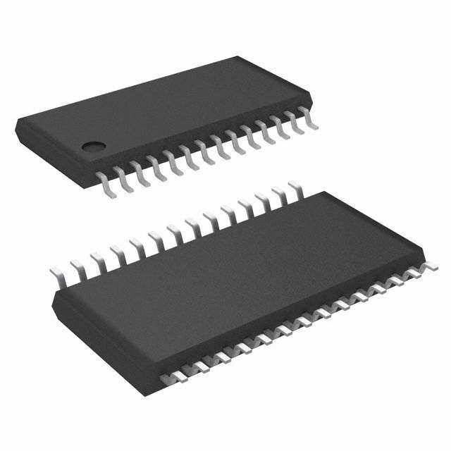
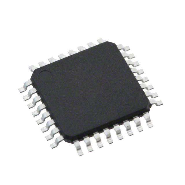
| 供应商器件封装 | 40-PDIP |
| 其它名称 | ATMEGA324PV10PU |
| 包装 | 管件 |
| 可用A/D通道 | 8 |
| 可编程输入/输出端数量 | 32 |
| 商标 | Atmel |
| 商标名 | ATMEGA |
| 处理器系列 | megaAVR |
| 外设 | 欠压检测/复位,POR,PWM,WDT |
| 安装风格 | Through Hole |
| 定时器数量 | 3 Timer |
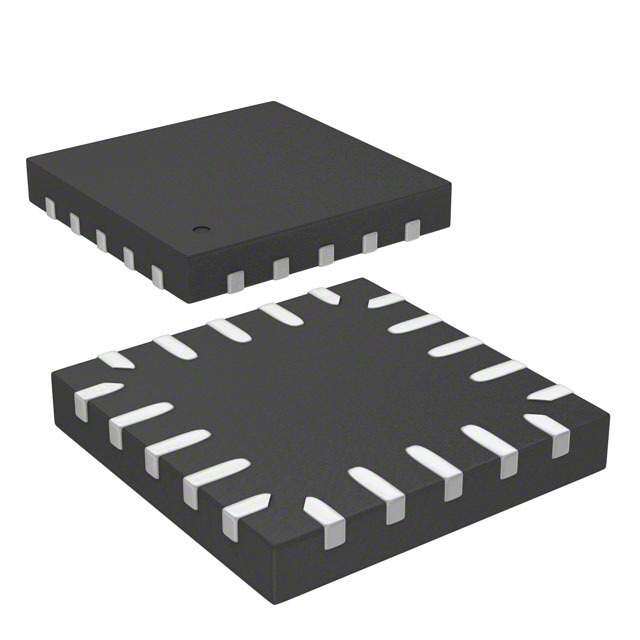
| 封装/外壳 | 40-DIP(0.600",15.24mm) |
| 封装/箱体 | PDIP-40 |
| 工作温度 | -40°C ~ 85°C |
| 工作电源电压 | 1.8 V to 5.5 V |
| 工厂包装数量 | 10 |
| 振荡器类型 | 内部 |
| 接口类型 | 2-Wire, JTAG, SPI, USART |
| 数据RAM大小 | 2 kB |
| 数据Ram类型 | SRAM |
| 数据ROM大小 | 1 kB |
| 数据Rom类型 | EEPROM |
| 数据总线宽度 | 8 bit |
| 数据转换器 | A/D 8x10b |
| 最大工作温度 | + 85 C |
| 最大时钟频率 | 10 MHz |
| 最小工作温度 | - 40 C |
| 标准包装 | 10 |
| 核心 | AVR |
| 核心处理器 | AVR |
| 核心尺寸 | 8-位 |
| 片上ADC | Yes |
| 电压-电源(Vcc/Vdd) | 1.8 V ~ 5.5 V |
| 电源电压-最大 | 5.5 V |
| 电源电压-最小 | 1.8 V |
| 程序存储器大小 | 32 kB |
| 程序存储器类型 | Flash |
| 程序存储容量 | 32KB(16K x 16) |
| 系列 | ATMEGA 324P |
| 输入/输出端数量 | 32 I/O |
| 连接性 | I²C, SPI, UART/USART |
| 速度 | 10MHz |
| 配用 | /product-detail/zh/ATSTK600-RC05/ATSTK600-RC05-ND/2271098/product-detail/zh/ATSTK600-TQFP44/ATSTK600-TQFP44-ND/1812223/product-detail/zh/ATSTK600/ATSTK600-ND/1812220/product-detail/zh/ATAVRISP2/ATAVRISP2-ND/898891 |


- 商务部:美国ITC正式对集成电路等产品启动337调查
- 曝三星4nm工艺存在良率问题 高通将骁龙8 Gen1或转产台积电
- 太阳诱电将投资9.5亿元在常州建新厂生产MLCC 预计2023年完工
- 英特尔发布欧洲新工厂建设计划 深化IDM 2.0 战略
- 台积电先进制程称霸业界 有大客户加持明年业绩稳了
- 达到5530亿美元!SIA预计今年全球半导体销售额将创下新高
- 英特尔拟将自动驾驶子公司Mobileye上市 估值或超500亿美元
- 三星加码芯片和SET,合并消费电子和移动部门,撤换高东真等 CEO
- 三星电子宣布重大人事变动 还合并消费电子和移动部门
- 海关总署:前11个月进口集成电路产品价值2.52万亿元 增长14.8%


PDF Datasheet 数据手册内容提取
8-bit AVR Microcontrollers ATmega324P/V DATASHEET SUMMARY Introduction The Atmel® picoPower® ATmega324P is a low-power CMOS 8-bit microcontroller based on the AVR® enhanced RISC architecture. By executing powerful instructions in a single clock cycle, the ATmega324P achieves throughputs close to 1MIPS per MHz. This empowers system designer to optimize the device for power consumption versus processing speed. Feature High Performance, Low Power Atmel® AVR® 8-Bit Microcontroller Family • Advanced RISC Architecture – 131 Powerful Instructions – Most Single Clock Cycle Execution – 32 x 8 General Purpose Working Registers – Fully Static Operation – Up to 20 MIPS Throughput at 20MHz – On-chip 2-cycle Multiplier • High Endurance Non-volatile Memory Segments – 32KBytes of In-System Self-Programmable Flash Program Memory – 1KBytes EEPROM – 2KBytes Internal SRAM – Write/Erase Cycles: 10,000 Flash/100,000 EEPROM – Data Retention: 20 Years at 85°C/100 Years at 25°C(1) – Optional Boot Code Section with Independent Lock Bits • In-System Programming by On-chip Boot Program • True Read-While-Write Operation – Programming Lock for Software Security • Atmel QTouch® Library Support – Capacitive Touch Buttons, Sliders and Wheels – QTouch and QMatrix acquisition Atmel-42743B-ATmega324P/V_Datasheet_Summary-08/2016
– Up to 64 Sense Channels • JTAG (IEEE std. 1149.1 Compliant) Interface – Boundary-scan Capabilities According to the JTAG Standard – Extensive On-chip Debug Support – Programming of Flash, EEPROM, Fuses, and Lock Bits through the JTAG Interface • Peripheral Features – Two 8-bit Timer/Counters with Separate Prescaler and Compare Mode – One 16-bit Timer/Counter with Separate Prescaler, Compare Mode, and Capture Mode – Real Time Counter with Separate Oscillator – Six PWM Channels – 8-channel 10-bit ADC • Differential Mode with Selectable Gain at 1×, 10× or 200× – One Byte-oriented 2-wire Serial Interface (Philips I2C compatible) – Two Programmable Serial USART – One Master/Slave SPI Serial Interface – Programmable Watchdog Timer with Separate On-chip Oscillator – On-chip Analog Comparator – Interrupt and Wake-up on Pin Change • Special Microcontroller Features – Power-on Reset and Programmable Brown-out Detection – Internal Calibrated RC Oscillator – External and Internal Interrupt Sources – Six Sleep Modes: Idle, ADC Noise Reduction, Power-save, Power-down, Standby, and Extended Standby • I/O and Packages – 32 Programmable I/O Lines – 40-pin PDIP – 44-lead TQFP – 44-pad VQFN/QFN • Operating Voltage: – 1.8 - 5.5V for ATmega324PV – 2.7 - 5.5V for ATmega324P • Speed Grades – ATmega324PV: • 0 - 4MHz @ 1.8V - 5.5V • 0 - 10MHz @ 2.7V - 5.5V – ATmega324P: • 0 - 10MHz @ 2.7V - 5.5V • 0 - 20MHz @ 4.5 - 5.5V • Power Consumption at 1MHz, 1.8V, 25°C – Active Mode: 0.4mA – Power-down Mode: 0.1μA – Power-save Mode: 0.6μA (Including 32kHz RTC) Atmel ATmega324P/V [DATASHEET] 2 Atmel-42743B-ATmega324P/V_Datasheet_Summary-08/2016
1. Refer to Data Retention. Related Links Data Retention on page 15 Atmel ATmega324P/V [DATASHEET] 3 Atmel-42743B-ATmega324P/V_Datasheet_Summary-08/2016
Table of Contents Introduction......................................................................................................................1 Feature............................................................................................................................1 1. Description.................................................................................................................5 2. Configuration Summary.............................................................................................6 3. Ordering Information .................................................................................................7 4. Block Diagram...........................................................................................................9 5. Pin Configurations...................................................................................................10 5.1. Pinout.........................................................................................................................................10 5.2. Pin Descriptions..........................................................................................................................11 6. I/O Multiplexing........................................................................................................13 7. General Information.................................................................................................15 7.1. Resources..................................................................................................................................15 7.2. Data Retention............................................................................................................................15 7.3. About Code Examples................................................................................................................15 7.4. Capacitive Touch Sensing..........................................................................................................15 8. Packaging Information.............................................................................................16 8.1. 40-pin PDIP................................................................................................................................16 8.2. 44-pin TQFP...............................................................................................................................17 8.3. 44-pin VQFN...............................................................................................................................18 Atmel ATmega324P/V [DATASHEET] 4 Atmel-42743B-ATmega324P/V_Datasheet_Summary-08/2016
1. Description The Atmel® ATmega324P is a low-power CMOS 8-bit microcontroller based on the AVR enhanced RISC architecture. By executing powerful instructions in a single clock cycle, the ATmega324P achieves throughputs close to 1MIPS per MHz. This empowers system designer to optimize the device for power consumption versus processing speed. The Atmel AVR® core combines a rich instruction set with 32 general purpose working registers. All the 32 registers are directly connected to the Arithmetic Logic Unit (ALU), allowing two independent registers to be accessed in a single instruction executed in one clock cycle. The resulting architecture is more code efficient while achieving throughputs up to ten times faster than conventional CISC microcontrollers. The ATmega324P provides the following features: 32Kbytes of In-System Programmable Flash with Read-While-Write capabilities, 1Kbytes EEPROM, 2Kbytes SRAM, 32 general purpose I/O lines, 32 general purpose working registers, Real Time Counter (RTC), three flexible Timer/Counters with compare modes and PWM, two serial programmable USARTs , one byte-oriented 2-wire Serial Interface (I2C), a 8- channel 10-bit ADC with optional differential input stage with programmable gain, a programmable Watchdog Timer with internal Oscillator, an SPI serial port, IEEE std. 1149.1 compliant JTAG test interface, also used for accessing the On-chip Debug system and programming and six software selectable power saving modes. The Idle mode stops the CPU while allowing the SRAM, Timer/Counters, SPI port, and interrupt system to continue functioning. The Power-down mode saves the register contents but freezes the Oscillator, disabling all other chip functions until the next interrupt or hardware reset. In Power-save mode, the asynchronous timer continues to run, allowing the user to maintain a timer base while the rest of the device is sleeping. The ADC Noise Reduction mode stops the CPU and all I/O modules except asynchronous timer and ADC to minimize switching noise during ADC conversions. In Standby mode, the crystal/resonator oscillator is running while the rest of the device is sleeping. This allows very fast start-up combined with low power consumption. In Extended Standby mode, both the main oscillator and the asynchronous timer continue to run. Atmel offers the QTouch® library for embedding capacitive touch buttons, sliders and wheels functionality into AVR microcontrollers. The patented charge-transfer signal acquisition offers robust sensing and includes fully debounced reporting of touch keys and includes Adjacent Key Suppression® (AKS™) technology for unambiguous detection of key events. The easy-to-use QTouch Suite toolchain allows you to explore, develop and debug your own touch applications. The device is manufactured using Atmel’s high density non-volatile memory technology. The On-chip ISP Flash allows the program memory to be reprogrammed In-System through an SPI serial interface, by a conventional nonvolatile memory programmer, or by an On-chip Boot program running on the AVR core. The Boot program can use any interface to download the application program in the Application Flash memory. Software in the Boot Flash section will continue to run while the Application Flash section is updated, providing true Read-While-Write operation. By combining an 8-bit RISC CPU with In-System Self-Programmable Flash on a monolithic chip, the Atmel ATmega324P is a powerful microcontroller that provides a highly flexible and cost effective solution to many embedded control applications. The ATmega324P is supported with a full suite of program and system development tools including: C Compilers, Macro Assemblers, Program Debugger/Simulators, In-Circuit Emulators, and Evaluation kits. Atmel ATmega324P/V [DATASHEET] 5 Atmel-42743B-ATmega324P/V_Datasheet_Summary-08/2016
2. Configuration Summary The table below compares the device series of feature and pin compatible devices, providing a seamless migration path. Table 2-1. Configuration Summary and Device Comparison Features ATmega164/V ATmega324/V ATmega644/V Pin Count 40/44 40/44 40/44 Flash (Bytes) 16K 32K 64K SRAM (Bytes) 1K 2K 4K EEPROM (Bytes) 512 1K 2K General Purpose I/O 32 32 32 Lines SPI 1 1 1 TWI (I2C) 1 1 1 USART 2 2 2 ADC 10-bit 15ksps 10-bit 15ksps 10-bit 15ksps ADC Channels 8 8 8 Analog Comparator 1 1 1 8-bit Timer/Counters 2 2 2 16-bit Timer/Counters 1 1 1 PWM channels 6 6 6 Packages PDIP PDIP PDIP TQFP TQFP TQFP VQFN/QFN VQFN/QFN VQFN/QFN Atmel ATmega324P/V [DATASHEET] 6 Atmel-42743B-ATmega324P/V_Datasheet_Summary-08/2016
3. Ordering Information Speed [MHz](3) Power Supply [V] Ordering Code(2) Package(1) Operational Range 10 1.8 - 5.5 Industrial ATmega324PV-10AU 44A (-40°C to 85°C) ATmega324PV-10AUR(4) 44A ATmega324PV-10PU 40P6 ATmega324PV-10MU 44M1 ATmega324PV-10MUR(4) 44M1 20 2.7 - 5.5 Industrial ATmega324P-20AU 44A (-40°C to 85°C) ATmega324P-20AUR(4) 44A ATmega324P-20PU 40P6 ATmega324P-20MU 44M1 ATmega324P-20MUR(4) 44M1 10 1.8 - 5.5 Industrial ATmega324PV-10AN 44A (-40°C to 105°C) ATmega324PV-10ANR(4) 44A ATmega324PV-10PN 40P6 ATmega324PV-10MN 44M1 ATmega324PV-10MNR(4) 44M1 20 2.7 - 5.5 Industrial ATmega324P-20AN 44A (-40°C to 105°C) ATmega324P-20ANR(4) 44A ATmega324P-20PN 40P6 ATmega324P-20MN 44M1 ATmega324P-20MNR(4) 44M1 Note: 1. This device can also be supplied in wafer form. Please contact your local Atmel sales office for detailed ordering information and minimum quantities. 2. Pb-free packaging, complies to the European Directive for Restriction of Hazardous Substances (RoHS directive). Also Halide free and fully Green. 3. Refer to Speed Grades for Speed vs. V CC 4. Tape & Reel. Atmel ATmega324P/V [DATASHEET] 7 Atmel-42743B-ATmega324P/V_Datasheet_Summary-08/2016
Package Type 40P6 40-pin, 0.600” Wide, Plastic Dual Inline Package (PDIP) 44A 44-lead, Thin (1.0mm) Plastic Quad Flat Package (TQFP) 44M1 44-pad, 7 × 7 × 1.0mm body, lead pitch 0.50mm, Thermally Enhanced Plastic Very Thin Quad Flat No- Lead (VQFN) Atmel ATmega324P/V [DATASHEET] 8 Atmel-42743B-ATmega324P/V_Datasheet_Summary-08/2016
4. Block Diagram Figure 4-1. Block Diagram SRAM TCK TTMDSI JTAG CPU TDO OCD Clock generation PA[7:0] TOSC1 32X.7O6S8kCHz Ca8lMibH RzC progNraVmMm ing FLASH NI/ POI/ROTS PPPBCD[[[777:::000]]] TOSC2 128kHz int O XTAL1 16MHz LP osc Power U XOSC External management T GPIOR[2:0] XTAL2 clock ancdo nctlrooclk DA EEPROM DA TC 0 TO0C0A T T (8-bit) OC0B A A VCC B B MISO Power U EEPROMIF U SPI MOSI Supervision Watchdog S S SSCSK RESET Timer POR/BOD & AIN0 RESET AC AIN1 GND Internal AACDOCMUX ADC[7:0] ADC Reference AREF RxD0 PCINT[31:0] EXTINT USART 0 TxD0 INT[2:0] XCK0 OC1A/B TC 1 RxD1 T1 (16-bit) USART 1 TxD1 ICP1 XCK1 OC2A TC 2 TWI SDA OC2B (8-bit async) SCL Atmel ATmega324P/V [DATASHEET] 9 Atmel-42743B-ATmega324P/V_Datasheet_Summary-08/2016
5. Pin Configurations 5.1. Pinout 5.1.1. PDIP (PCINT8/XCK0/T0) (ADC0/PCINT0) (PCINT9/CLKO/T1) (ADC1/PCINT1) (PCINT10/INT2/AIN0) (ADC2/PCINT2) (PCINT11/OC0A/AIN1) (ADC3/PCINT3) (PCINT12/OC0B/ (ADC4/PCINT4) (PCINT13/MOSI) (ADC5/PCINT5) (PCINT14/MISO) (ADC6/PCINT6) (PCINT15//SCK) (ADC7/PCINT7) XTAL2 (TOSC2/PCINT23) XTAL1 (TOSC1/PCINT22) (PCINT24/RXD0) (TDI/PCINT21) (PCINT25/TXD0) (TDO/PCINT20) (PCINT26/RXD1/INT0) (TMS/PCINT19) Power (PCINT27/TXD1/INT1) (TCK/PCINT18) Ground Programming/debug (PCINT28/XCK1/OC1B) (SDA/PCINT17) Digital (PCINT29/OC1A) (SCL/PCINT16) Analog (PCINT30/OC2B/ICP1) (OC2A/PCINT31) Crystal/Osc Atmel ATmega324P/V [DATASHEET] 10 Atmel-42743B-ATmega324P/V_Datasheet_Summary-08/2016
5.1.2. TQFN and QFN ) 1 ) 1 0 12) NT T1 9) 8) Power T I N T T Ground B/PCIN C0A/PC T2/PCI O/PCIN 0/PCIN CINT0) CINT1) CINT2) CINT3) Programming/debug 0 O N K T P P P P Digital S/OC IN1/ IN0/I 1/CL CK0/ DC0/ DC1/ DC2/ DC3/ S A A T X A A A A Analog B4 ( B3 ( B2 ( B1 ( B0 ( ND CC A0 ( A1 ( A2 ( A3 ( Crystal/Osc P P P P P G V P P P P 4 3 2 1 0 9 8 7 6 5 4 4 4 4 4 4 3 3 3 3 3 3 (PCINT13/MOSI) PB5 1 33 PA4 (ADC4/PCINT4) (PCINT14/MISO) PB6 2 32 PA5 (ADC5/PCINT5) (PCINT15/SCK) PB7 3 31 PA6 (ADC6/PCINT6) RESET 4 30 PA7 (ADC7/PCINT7) VCC 5 29 AREF GND 6 28 GND XTAL2 7 27 AVCC XTAL1 8 26 PC7 (TOSC2/PCINT23) (PCINT24/RXD0) PD0 9 25 PC6 (TOSC1/PCINT22) (PCINT25/TXD0) PD1 10 24 PC5 (TDI/PCINT21) (PCINT26/RXD1/INT0) PD2 11 23 PC4 (TDO/PCINT20) 2 3 4 5 6 7 8 9 0 1 2 1 1 1 1 1 1 1 1 2 2 2 D3 D4 D5 D6 D7 C D C0 C1 C2 C3 P P P P P C N P P P P (PCINT27/TXD1/INT1) (PCINT28/XCK1/OC1B) (PCINT29/OC1A) (PCINT30/OC2B/ICP1) (PCINT31/OC2A) V G (PCINT16/SCL) (PCINT17/SDA) (PCINT18/TCK) (PCINT19/TMS) 5.2. Pin Descriptions 5.2.1. VCC Digital supply voltage. 5.2.2. GND Ground. 5.2.3. Port A (PA[7:0]) This port serves as analog inputs to the Analog-to-digital Converter. Atmel ATmega324P/V [DATASHEET] 11 Atmel-42743B-ATmega324P/V_Datasheet_Summary-08/2016
This is an 8-bit, bi-directional I/O port with internal pull-up resistors, individually selectable for each bit. The output buffers have symmetrical drive characteristics, with both high sink and source capability. As inputs, the port pins that are externally pulled low will source current if pull-up resistors are activated. Port pins are tri-stated when a reset condition becomes active, even if the clock is not running. 5.2.4. Port B (PB[7:0]) This is an 8-bit, bi-directional I/O port with internal pull-up resistors, individually selectable for each bit. The output buffers have symmetrical drive characteristics, with both high sink and source capability. As inputs, the port pins that are externally pulled low will source current if pull-up resistors are activated. Port pins are tri-stated when a reset condition becomes active, even if the clock is not running. This port also serves the functions of various special features. 5.2.5. Port C (PC[7:0]) This is an 8-bit, bi-directional I/O port with internal pull-up resistors, individually selectable for each bit. The output buffers have symmetrical drive characteristics, with both high sink and source capability. As inputs, the port pins that are externally pulled low will source current if pull-up resistors are activated. Port pins are tri-stated when a reset condition becomes active, even if the clock is not running. This port also serves the functions of the JTAG interface, along with special features. 5.2.6. Port D (PD[7:0]) This is an 8-bit, bi-directional I/O port with internal pull-up resistors, individually selectable for each bit. The output buffers have symmetrical drive characteristics, with both high sink and source capability. As inputs, the port pins that are externally pulled low will source current if pull-up resistors are activated. Port pins are tri-stated when a reset condition becomes active, even if the clock is not running. This port also serves the functions of various special features. 5.2.7. RESET Reset input. A low level on this pin for longer than the minimum pulse length will generate a reset, even if the clock is not running. Shorter pulses are not guaranteed to generate a reset. 5.2.8. XTAL1 Input to the inverting Oscillator amplifier and input to the internal clock operating circuit. 5.2.9. XTAL2 Output from the inverting Oscillator amplifier. 5.2.10. AVCC AVCC is the supply voltage pin for Port A and the Analog-to-digital Converter. It should be externally connected to V , even if the ADC is not used. If the ADC is used, it should be connected to V through CC CC a low-pass filter. 5.2.11. AREF This is the analog reference pin for the Analog-to-digital Converter. Atmel ATmega324P/V [DATASHEET] 12 Atmel-42743B-ATmega324P/V_Datasheet_Summary-08/2016
6. I/O Multiplexing Each pin is by default controlled by the PORT as a general purpose I/O and alternatively it can be assigned to one of the peripheral functions. The following table describes the peripheral signals multiplexed to the PORT I/O pins. Table 6-1. PORT Function Multiplexing 32-pin TQFP/ QFN/ MLF Pin # 40-pin PDIP Pin # PAD EXTINT PCINT ADC/AC OSC T/C # 0 T/C # 1 USART I2C SPI JTAG 1 6 PB[5] PCINT13 MOSI 2 7 PB[6] PCINT14 MISO 3 8 PB[7] PCINT15 SCK 4 9 RESET 5 10 VCC 6 11 GND 7 12 XTAL2 8 13 XTAL1 9 14 PD[0] PCINT24 RxD0 10 15 PD[1] PCINT25 TxD0 11 16 PD[2] INT0 PCINT26 RxD1 12 17 PD[3] INT1 PCINT27 TXD1 13 18 PD[4] PCINT28 OC1B XCK1 14 19 PD[5] PCINT29 OC1A 15 20 PD[6] PCINT30 OC2B ICP1 16 21 PD[7] PCINT31 OC2A 17 - VCC RxD2 MISO1 18 - GND TxD2 MOSI1 19 22 PC[0] PCINT16 SCL 20 23 PC[1] PCINT17 SDA 21 24 PC[2] PCINT18 TCK 22 25 PC[3] PCINT19 TMS 23 26 PC[4] PCINT20 TDO 24 27 PC[5] PCINT21 TDI 25 28 PC[6] PCINT22 TOSC1 26 29 PC[7] PCINT23 TOSC2 27 30 AVCC 28 31 GND 29 32 AREF AREF 30 33 PA[7] PCINT7 ADC7 31 34 PA[6] PCINT6 ADC6 32 35 PA[5] PCINT5 ADC5 33 36 PA[4] PCINT4 ADC4 34 37 PA[3] PCINT3 ADC3 Atmel ATmega324P/V [DATASHEET] 13 Atmel-42743B-ATmega324P/V_Datasheet_Summary-08/2016
32-pin TQFP/ QFN/ MLF Pin # 40-pin PDIP Pin # PAD EXTINT PCINT ADC/AC OSC T/C # 0 T/C # 1 USART I2C SPI JTAG 35 38 PA[2] PCINT2 ADC2 36 39 PA[1] PCINT1 ADC1 37 40 PA[0] PCINT0 ADC0 38 - VCC SDA1 39 - GND SCL1 40 1 PB[0] PCINT8 T0 XCK0 41 2 PB[1] PCINT9 CLKO T1 42 3 PB[2] INT2 PCINT10 AIN0 43 4 PB[3] PCINT11 AIN1 OC0A 44 5 PB[4] PCINT12 OC0B SS - - GND - - GND - - GND - - GND - - GND Atmel ATmega324P/V [DATASHEET] 14 Atmel-42743B-ATmega324P/V_Datasheet_Summary-08/2016
7. General Information 7.1. Resources A comprehensive set of development tools, application notes, and datasheets are available for download on http://www.atmel.com/avr. 7.2. Data Retention Reliability Qualification results show that the projected data retention failure rate is much less than 1 PPM over 20 years at 85°C or 100 years at 25°C. 7.3. About Code Examples This documentation contains simple code examples that briefly show how to use various parts of the device. These code examples assume that the part specific header file is included before compilation. Be aware that not all C compiler vendors include bit definitions in the header files and interrupt handling in C is compiler dependent. Confirm with the C compiler documentation for more details. For I/O Registers located in extended I/O map, “IN”, “OUT”, “SBIS”, “SBIC”, “CBI”, and “SBI” instructions must be replaced with instructions that allow access to extended I/O. Typically “LDS” and “STS” combined with “SBRS”, “SBRC”, “SBR”, and “CBR”. 7.4. Capacitive Touch Sensing 7.4.1. QTouch Library The Atmel® QTouch® Library provides a simple to use solution to realize touch sensitive interfaces on most Atmel AVR® microcontrollers. The QTouch Library includes support for the Atmel QTouch and Atmel QMatrix® acquisition methods. Touch sensing can be added to any application by linking the appropriate Atmel QTouch Library for the AVR Microcontroller. This is done by using a simple set of APIs to define the touch channels and sensors, and then calling the touch sensing API’s to retrieve the channel information and determine the touch sensor states. The QTouch Library is FREE and downloadable from the Atmel website at the following location: http:// www.atmel.com/technologies/touch/. For implementation details and other information, refer to the Atmel QTouch Library User Guide - also available for download from the Atmel website. Atmel ATmega324P/V [DATASHEET] 15 Atmel-42743B-ATmega324P/V_Datasheet_Summary-08/2016
8. Packaging Information 8.1. 40-pin PDIP D PIN 1 E1 A SEATING PLANE A1 L B B1 e E COMMON DIMENSIONS 0º ~ 15º REF (Unit of Measure = mm) C SYMBOL MIN NOM MAX NOTE eB A – – 4.826 A1 0.381 – – D 52.070 – 52.578 Note 2 E 15.240 – 15.875 E1 13.462 – 13.970 Note 2 B 0.356 – 0.559 B1 1.041 – 1.651 Notes: L 3.048 – 3.556 1. This package conforms to JEDEC reference MS-011, Variation AC. C 0.203 – 0.381 2. Dimensions D and E1 do not include mold Flash or Protrusion. Mold Flash or Protrusion shall not exceed 0.25mm (0.010"). eB 15.494 – 17.526 e 2.540 TYP 13/02/2014 40P6, 40-lead (0.600"/15.24mm Wide) Plastic Dual Inline Package (PDIP) 40P6 C Atmel ATmega324P/V [DATASHEET] 16 Atmel-42743B-ATmega324P/V_Datasheet_Summary-08/2016
8.2. 44-pin TQFP PIN 1 IDENTIFIER PIN 1 e B E1 E D1 D C 0°~7° A1 A2 A L COMMON DIMENSIONS (Unit of Measure = mm) SYMBOL MIN NOM MAX NOTE A – – 1.20 A1 0.05 – 0.15 A2 0.95 1.00 1.05 D 11.75 12.00 12.25 D1 9.90 10.00 10.10 Note 2 Notes: E 11.75 12.00 12.25 1. This package conforms to JEDEC reference MS-026, Variation ACB. E1 9.90 10.00 10.10 Note 2 2. Dimensions D1 and E1 do not include mold protrusion. Allowable B 0.30 0.37 0.45 protrusion is 0.25mm per side. Dimensions D1 and E1 are maximum plastic body size dimensions including mold mismatch. C 0.09 (0.17) 0.20 3. Lead coplanarity is 0.10mm maximum. L 0.45 0.60 0.75 e 0.80 TYP 06/02/2014 44A,44-lead, 10 x 10mm body size, 1.0mm body thickness, 44A C 0.8 mm lead pitch, thin profile plastic quad flat package (TQFP) Atmel ATmega324P/V [DATASHEET] 17 Atmel-42743B-ATmega324P/V_Datasheet_Summary-08/2016
8.3. 44-pin VQFN D Marked Pin# 1 ID E SEATING PLANE A1 TOP VIEW A3 A K L D2 Pin #1 Corner SIDE VIEW 1 Option A Pin #1 COMMON DIMENSIONS Triangle 2 (Unit of Measure = mm) 3 SYMBOL MIN NOM MAX NOTE A 0.80 0.90 1.00 E2 Option B A1 – 0.02 0.05 Pin #1 Chamfer (C 0.30) A3 0.20 REF b 0.18 0.23 0.30 D 6.90 7.00 7.10 K Option C Pin #1 D2 5.00 5.20 5.40 b e N(0o.2tc0h R ) E 6.90 7.00 7.10 BOTTOM VIEW E2 5.00 5.20 5.40 e 0.50 BSC L 0.59 0.64 0.69 Note: JEDEC Standard MO-220, Fig . 1 (SAW Singulation) VKKD-3. K 0.20 0.26 0.41 9/26/08 TITLE GPC DRAWING NO. REV. Package Drawing Contact: 44M1, 44-pad, 7 x 7 x 1.0mm body, lead avr@atmel.com pitch 0.50mm, 5.20mm exposed pad, thermally ZWS 44M1 H enhanced plastic very thin quad flat no lead package (VQFN) Atmel ATmega324P/V [DATASHEET] 18 Atmel-42743B-ATmega324P/V_Datasheet_Summary-08/2016
Atmel Corporation 1600 Technology Drive, San Jose, CA 95110 USA T: (+1)(408) 441.0311 F: (+1)(408) 436.4200 | www.atmel.com © 2016 Atmel Corporation. / Rev.: Atmel-42743B-ATmega324P/V_Datasheet_Summary-08/2016 Atmel®, Atmel logo and combinations thereof, Enabling Unlimited Possibilities®, AVR®, and others are registered trademarks or trademarks of Atmel Corporation in U.S. and other countries. Other terms and product names may be trademarks of others. DISCLAIMER: The information in this document is provided in connection with Atmel products. No license, express or implied, by estoppel or otherwise, to any intellectual property right is granted by this document or in connection with the sale of Atmel products. EXCEPT AS SET FORTH IN THE ATMEL TERMS AND CONDITIONS OF SALES LOCATED ON THE ATMEL WEBSITE, ATMEL ASSUMES NO LIABILITY WHATSOEVER AND DISCLAIMS ANY EXPRESS, IMPLIED OR STATUTORY WARRANTY RELATING TO ITS PRODUCTS INCLUDING, BUT NOT LIMITED TO, THE IMPLIED WARRANTY OF MERCHANTABILITY, FITNESS FOR A PARTICULAR PURPOSE, OR NON-INFRINGEMENT. IN NO EVENT SHALL ATMEL BE LIABLE FOR ANY DIRECT, INDIRECT, CONSEQUENTIAL, PUNITIVE, SPECIAL OR INCIDENTAL DAMAGES (INCLUDING, WITHOUT LIMITATION, DAMAGES FOR LOSS AND PROFITS, BUSINESS INTERRUPTION, OR LOSS OF INFORMATION) ARISING OUT OF THE USE OR INABILITY TO USE THIS DOCUMENT, EVEN IF ATMEL HAS BEEN ADVISED OF THE POSSIBILITY OF SUCH DAMAGES. Atmel makes no representations or warranties with respect to the accuracy or completeness of the contents of this document and reserves the right to make changes to specifications and products descriptions at any time without notice. Atmel does not make any commitment to update the information contained herein. Unless specifically provided otherwise, Atmel products are not suitable for, and shall not be used in, automotive applications. Atmel products are not intended, authorized, or warranted for use as components in applications intended to support or sustain life. SAFETY-CRITICAL, MILITARY, AND AUTOMOTIVE APPLICATIONS DISCLAIMER: Atmel products are not designed for and will not be used in connection with any applications where the failure of such products would reasonably be expected to result in significant personal injury or death (“Safety-Critical Applications”) without an Atmel officer's specific written consent. Safety-Critical Applications include, without limitation, life support devices and systems, equipment or systems for the operation of nuclear facilities and weapons systems. Atmel products are not designed nor intended for use in military or aerospace applications or environments unless specifically designated by Atmel as military-grade. Atmel products are not designed nor intended for use in automotive applications unless specifically designated by Atmel as automotive-grade.