ICGOO在线商城 > 集成电路(IC) > 嵌入式 - 微控制器 > ATXMEGA32A4U-AUR
/ATXMEGA32A4U-AUR.jpg)
 Datasheet下载
- 型号: ATXMEGA32A4U-AUR
- 制造商: Atmel
- 库位|库存: xxxx|xxxx
- 要求:
| 数量阶梯 | 香港交货 | 国内含税 |
| +xxxx | $xxxx | ¥xxxx |
查看当月历史价格
查看今年历史价格
ATXMEGA32A4U-AUR产品简介:
ICGOO电子元器件商城为您提供ATXMEGA32A4U-AUR由Atmel设计生产,在icgoo商城现货销售,并且可以通过原厂、代理商等渠道进行代购。 ATXMEGA32A4U-AUR价格参考。AtmelATXMEGA32A4U-AUR封装/规格:嵌入式 - 微控制器, AVR AVR® XMEGA® A4U Microcontroller IC 8/16-Bit 32MHz 32KB (16K x 16) FLASH 44-TQFP (10x10)。您可以下载ATXMEGA32A4U-AUR参考资料、Datasheet数据手册功能说明书,资料中有ATXMEGA32A4U-AUR 详细功能的应用电路图电压和使用方法及教程。
ATXMEGA32A4U-AUR是Microchip Technology旗下的一款高性能、低功耗的8位AVR微控制器,属于XMEGA系列。该芯片广泛应用于对性能、集成度和能效要求较高的嵌入式系统中。

典型应用场景包括:工业控制设备,如PLC模块、传感器接口和自动化控制器,得益于其丰富的外设和高抗干扰能力;智能仪表,如电表、水表和气表,利用其低功耗特性和集成的实时时钟(RTC)与LCD驱动功能,适合电池供电的长期运行设备;消费类电子产品,如家用电器控制面板、便携式设备和智能家居节点,可实现触摸感应、显示控制和通信功能;通信接口应用,因其内置USB 2.0全速接口、多种串行通信模块(UART、SPI、I²C),适用于需要与PC或其他设备进行数据交换的场景;此外,还可用于医疗设备、楼宇自动化和小型物联网终端设备。

ATXMEGA32A4U-AUR具备32KB闪存、4KB SRAM、多种定时器、高精度ADC/DAC及DMA控制器,支持多种低功耗模式,使其在复杂任务处理与节能需求之间实现良好平衡。其QFN封装形式节省空间,适合紧凑型设计。综上,该微控制器适用于中等复杂度、强调集成性与低功耗的嵌入式应用领域。
| 参数 | 数值 |
| 产品目录 | 集成电路 (IC) |
| 描述 | IC MCU 8BIT 32KB FLASH 44TQFP |
| EEPROM容量 | 2K x 8 |
| 产品分类 | |
| I/O数 | 34 |
| 品牌 | Atmel |
| 数据手册 | |
| 产品图片 |
|
| 产品型号 | ATXMEGA32A4U-AUR |
| PCN设计/规格 | |
| RAM容量 | 4K x 8 |
| rohs | 无铅 / 符合限制有害物质指令(RoHS)规范要求 |
| 产品系列 | AVR® XMEGA |
| 产品培训模块 | http://www.digikey.cn/PTM/IndividualPTM.page?site=cn&lang=zhs&ptm=26162http://www.digikey.cn/PTM/IndividualPTM.page?site=cn&lang=zhs&ptm=26159http://www.digikey.cn/PTM/IndividualPTM.page?site=cn&lang=zhs&ptm=26180 |
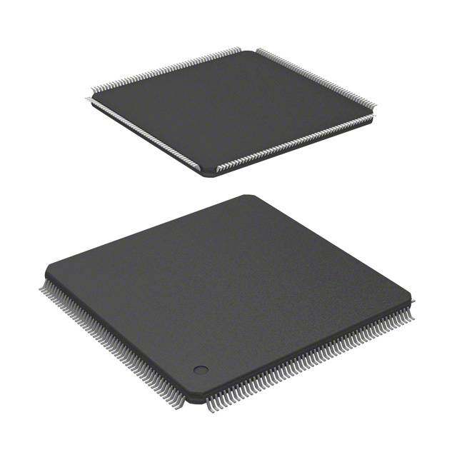
| 供应商器件封装 | 44-TQFP |
| 其它名称 | ATXMEGA32A4U-AURCT |
| 包装 | 剪切带 (CT) |
| 外设 | 欠压检测/复位,DMA,POR,PWM,WDT |
| 封装/外壳 | 44-TQFP |
| 工作温度 | -40°C ~ 85°C |
| 振荡器类型 | 内部 |
| 数据转换器 | A/D 12x12b,D/A 2x12b |
| 标准包装 | 1 |
| 核心处理器 | AVR |
| 核心尺寸 | 8/16-位 |
| 电压-电源(Vcc/Vdd) | 1.6 V ~ 3.6 V |
| 程序存储器类型 | 闪存 |
| 程序存储容量 | 32KB(16K x 16) |
| 连接性 | I²C, IrDA, SPI, UART/USART, USB |
| 速度 | 32MHz |


- 商务部:美国ITC正式对集成电路等产品启动337调查
- 曝三星4nm工艺存在良率问题 高通将骁龙8 Gen1或转产台积电
- 太阳诱电将投资9.5亿元在常州建新厂生产MLCC 预计2023年完工
- 英特尔发布欧洲新工厂建设计划 深化IDM 2.0 战略
- 台积电先进制程称霸业界 有大客户加持明年业绩稳了
- 达到5530亿美元!SIA预计今年全球半导体销售额将创下新高
- 英特尔拟将自动驾驶子公司Mobileye上市 估值或超500亿美元
- 三星加码芯片和SET,合并消费电子和移动部门,撤换高东真等 CEO
- 三星电子宣布重大人事变动 还合并消费电子和移动部门
- 海关总署:前11个月进口集成电路产品价值2.52万亿元 增长14.8%


PDF Datasheet 数据手册内容提取
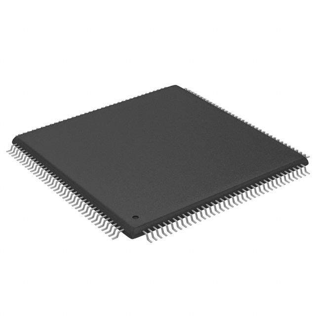
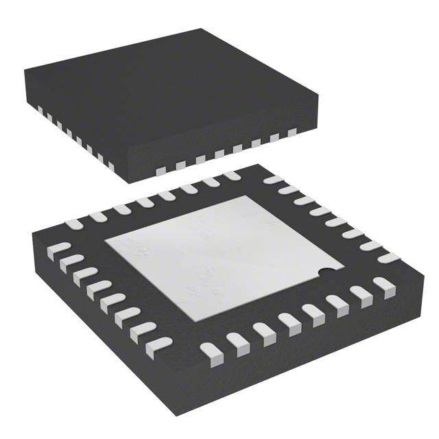
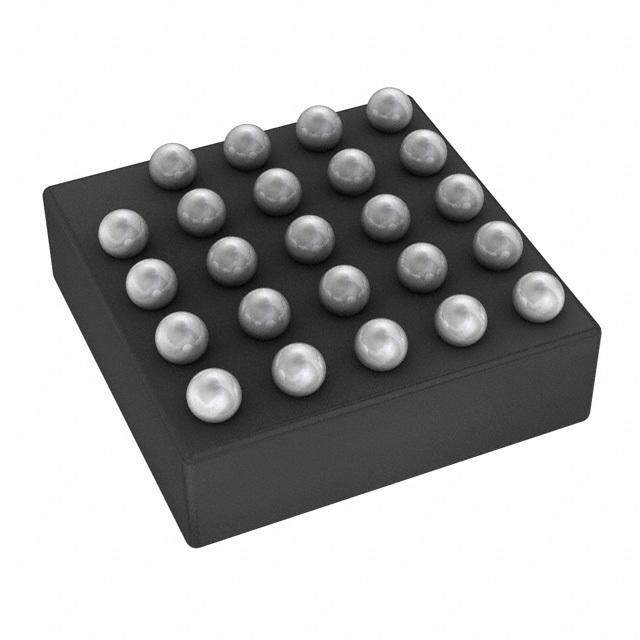
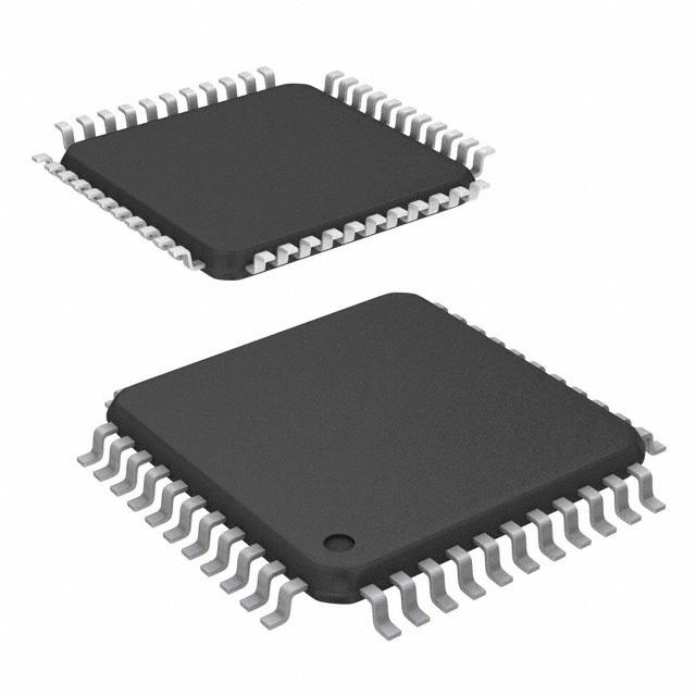
8/16-bit Atmel XMEGA Microcontroller ATxmega128A4U / ATxmega64A4U / ATxmega32A4U / ATxmega16A4U Features (cid:122) High-performance, low-power Atmel® AVR® XMEGA® 8/16-bit Microcontroller (cid:122) Nonvolatile program and data memories (cid:122) 16K - 128KB of in-system self-programmable flash (cid:122) 4K - 8KB boot section (cid:122) 1K - 2KB EEPROM (cid:122) 2K - 8KB internal SRAM (cid:122) Peripheral Features (cid:122) Four-channel DMA controller (cid:122) Eight-channel event system (cid:122) Five 16-bit timer/counters (cid:122) Three timer/counters with 4 output compare or input capture channels (cid:122) Two timer/counters with 2 output compare or input capture channels (cid:122) High-resolution extensions on all timer/counters (cid:122) Advanced waveform extension (AWeX) on one timer/counter (cid:122) One USB device interface (cid:122) USB 2.0 full speed (12Mbps) and low speed (1.5Mbps) device compliant (cid:122) 32 Endpoints with full configuration flexibility (cid:122) Five USARTs with IrDA support for one USART (cid:122) Two Two-wire interfaces with dual address match (I2C and SMBus compatible) (cid:122) Two serial peripheral interfaces (SPIs) (cid:122) AES and DES crypto engine (cid:122) CRC-16 (CRC-CCITT) and CRC-32 (IEEE® 802.3) generator (cid:122) 16-bit real time counter (RTC) with separate oscillator (cid:122) One twelve-channel, 12-bit, 2msps Analog to Digital Converter (cid:122) One two-channel, 12-bit, 1msps Digital to Analog Converter (cid:122) Two Analog Comparators with window compare function, and current sources (cid:122) External interrupts on all general purpose I/O pins (cid:122) Programmable watchdog timer with separate on-chip ultra low power oscillator (cid:122) QTouch® library support (cid:122) Capacitive touch buttons, sliders and wheels (cid:122) Special microcontroller features (cid:122) Power-on reset and programmable brown-out detection (cid:122) Internal and external clock options with PLL and prescaler (cid:122) Programmable multilevel interrupt controller (cid:122) Five sleep modes (cid:122) Programming and debug interfaces (cid:122) PDI (program and debug interface) (cid:122) I/O and packages (cid:122) 34 Programmable I/O pins (cid:122) 44 - lead TQFP (cid:122) 44 - pad VQFN/QFN (cid:122) 49 - ball VFBGA (cid:122) Operating voltage (cid:122) 1.6 – 3.6V (cid:122) Operating frequency (cid:122) 0 – 12MHz from 1.6V (cid:122) 0 – 32MHz from 2.7V Atmel-8387H-AVR-ATxmega16A4U-34A4U-64A4U-128A4U-Datasheet_09/2014
1. Ordering Information Ordering code Flash (bytes) EEPROM (bytes) SRAM (bytes) Speed (MHz) Power supply Package (1)(2)(3) Temp. ATxmega128A4U-AU 128K + 8K 2K 8K ATxmega128A4U-AUR(4) 128K + 8K 2K 8K ATxmega64A4U-AU 64K + 4K 2K 4K ATxmega64A4U-AUR(4) 64K + 4K 2K 4K 44A ATxmega32A4U-AU 32K + 4K 1K 4K ATxmega32A4U-AUR(4) 32K + 4K 1K 4K ATxmega16A4U-AU 16K + 4K 1K 2K ATxmega16A4U-AUR(4) 16K + 4K 1K 2K ATxmega128A4U-MH 128K + 8K 2K 8K ATxmega128A4U-MHR(4) 128K + 8K 2K 8K PW ATxmega64A4U-MH 64K + 4K 2K 4K ATxmega64A4U-MHR(4) 64K + 4K 2K 4K 32 1.6 - 3.6V -40°C - 85°C ATxmega32A4U-MH 32K + 4K 1K 4K ATxmega32A4U-MHR(4) 32K + 4K 1K 4K 44M1 ATxmega16A4U-MH 16K + 4K 1K 2K ATxmega16A4U-MHR(4) 16K + 4K 1K 2K ATxmega128A4U-CU 128K + 8K 2K 8K ATxmega128A4U-CUR(4) 128K + 8K 2K 8K ATxmega64A4U-CU 64K + 4K 2K 4K ATxmega64A4U-CUR(4) 64K + 4K 2K 4K 49C2 ATxmega32A4U-CU 32K + 4K 1K 4K ATxmega32A4U-CUR(4) 32K + 4K 1K 4K ATxmega16A4U-CU 16K + 4K 1K 2K ATxmega16A4U-CUR(4) 16K + 4K 1K 2K XMEGA A4U [DATASHEET] 2 Atmel-8387H-AVR-ATxmega16A4U-34A4U-64A4U-128A4U-Datasheet_09/2014
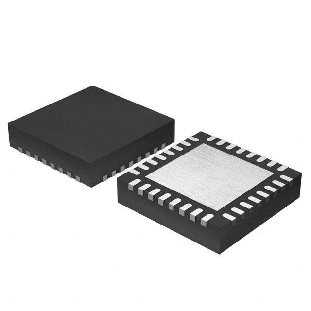
Ordering code Flash (bytes) EEPROM (bytes) SRAM (bytes) Speed (MHz) Power supply Package (1)(2)(3) Temp. ATxmega128A4U-AN 128K + 8K 2K 8K ATxmega128A4U-ANR(4) 128K + 8K 2K 8K ATxmega64A4U-AN 64K + 4K 2K 4K ATxmega64A4U-ANR(4) 64K + 4K 2K 4K 44A ATxmega32A4U-AN 32K + 4K 1K 4K ATxmega32A4U-ANR(4) 32K + 4K 1K 4K ATxmega16A4U-AN 16K + 4K 1K 2K ATxmega16A4U-ANR(4) 16K + 4K 1K 2K 32 1.6 - 3.6V 0°C - 105°C ATxmega128A4U-M7 128K + 8K 2K 8K ATxmega128A4U-M7R(4) 128K + 8K 2K 8K PW ATxmega64A4U-M7 64K + 4K 2K 4K ATxmega64A4U-M7R(4) 64K + 4K 2K 4K ATxmega32A4U-M7 32K + 4K 1K 4K ATxmega32A4U-M7R(4) 32K + 4K 1K 4K 44M1 ATxmega16A4U-M7 16K + 4K 1K 2K ATxmega16A4U-M7R(4) 16K + 4K 1K 2K Notes: 1. This device can also be supplied in wafer form. Please contact your local Atmel sales office for detailed ordering information. 2. Pb-free packaging, complies to the European Directive for Restriction of Hazardous Substances (RoHS directive). Also Halide free and fully Green. 3. For packaging information, see “Instruction Set Summary” on page 63. 4. Tape and Reel Package Type 44A 44-Lead, 10 x 10mm body size, 1.0mm body thickness, 0.8mm lead pitch, thin profile plastic quad flat package (TQFP) 44M1 44-Pad, 7x7x1mm body, lead pitch 0.50mm, 5.20mm exposed pad, thermally enhanced plastic very thin quad no lead package (VQFN) PW 44-Pad, 7x7x1mm body, lead pitch 0.50mm, 5.20mm exposed pad, thermally enhanced plastic very thin quad no lead package (VQFN) 49C2 49-Ball (7 x 7 Array), 0.65mm Pitch, 5.0 x 5.0 x 1.0mm, very thin, fine-pitch ball grid array package (VFBGA) Typical Applications Industrial control Climate control Low power battery applications Factory automation RF and ZigBee® Power tools Building control USB connectivity HVAC Board control Sensor control Utility metering White goods Optical Medical applications XMEGA A4U [DATASHEET] 3 Atmel-8387H-AVR-ATxmega16A4U-34A4U-64A4U-128A4U-Datasheet_09/2014
2. Pinout/Block Diagram Figure 2-1. Block Diagram and QFN/TQFP pinout Power Programming, debug, test Ground External clock / Crystal pins I Digital function General Purpose I/O D P Analog function / Oscillators / T C E C D A4 A3 A2 A1 A0 V N R1 R0 ES DI P P P P P A G P P R P 4 3 2 1 0 9 8 7 6 5 4 4 4 4 4 4 3 3 3 3 3 3 Port R XOSC TOSC PA5 1 33 PE3 DATA BUS PA6 2 OSC/CLK Internal Power 32 PE2 Watchdog Control oscillators Supervision AREF PA7 3 ort A ADC CoSnltereopller RCeoaul nTtimere WaTticmhedrog CoRnetrsoeltler 31 VCC P AC0:1 PB0 4 30 GND Event System Crypto / Prog/Debug OCD Controller CRC Interface PB1 5 29 PE1 Interrupt BUS AREF Controller matrix B PB2 6 Port DAC Internal CPU DMA 28 PE0 references Controller PB3 7 27 PD7 FLASH EEPROM SRAM GND 8 26 PD6 VCC 9 DATA BUS 25 PD5 EVENT ROUTING NETWORK PC0 10 24 PD4 1 1 PC1 11 IRCOM TC0:1 USART0: SPI TWI TC0:1 USART0: SPI USB TC0 USART0 TWI 23 PD3 Port C Port D Port E 2 3 4 5 6 7 8 9 0 1 2 1 1 1 1 1 1 1 1 2 2 2 2 3 4 5 6 7 D C 0 1 2 C C C C C C D D D N C P P P P P P P P P G V Note: 1. For full details on pinout and pin functions refer to “Pinout and Pin Functions” on page 55. XMEGA A4U [DATASHEET] 4 Atmel-8387H-AVR-ATxmega16A4U-34A4U-64A4U-128A4U-Datasheet_09/2014
Figure 2-2. BGA pinout Top view Bottom view 1 2 3 4 5 6 7 7 6 5 4 3 2 1 A A B B C C D D E E F F G G Table 2-1. BGA pinout 1 2 3 4 5 6 7 A PA3 AVCC GND PR1 PR0 PDI_DATA PE3 RESET/ B PA4 PA1 PA0 GND PE2 VCC PDI_CLK C PA5 PA2 PA6 PA7 GND PE1 GND D PB1 PB2 PB3 PB0 GND PD7 PE0 E GND GND PC3 GND PD4 PD5 PD6 F VCC PC0 PC4 PC6 PD0 PD1 PD3 G PC1 PC2 PC5 PC7 GND VCC PD2 XMEGA A4U [DATASHEET] 5 Atmel-8387H-AVR-ATxmega16A4U-34A4U-64A4U-128A4U-Datasheet_09/2014
3. Overview The Atmel AVR XMEGA is a family of low power, high performance, and peripheral rich 8/16-bit microcontrollers based on the AVR enhanced RISC architecture. By executing instructions in a single clock cycle, the AVR XMEGA devices achieve CPU throughput approaching one million instructions per second (MIPS) per megahertz, allowing the system designer to optimize power consumption versus processing speed. The AVR CPU combines a rich instruction set with 32 general purpose working registers. All 32 registers are directly connected to the arithmetic logic unit (ALU), allowing two independent registers to be accessed in a single instruction, executed in one clock cycle. The resulting architecture is more code efficient while achieving throughputs many times faster than conventional single-accumulator or CISC based microcontrollers. The AVR XMEGA A4U devices provide the following features: in-system programmable flash with read-while-write capabilities; internal EEPROM and SRAM; four-channel DMA controller, eight-channel event system and programmable multilevel interrupt controller, 34 general purpose I/O lines, 16-bit real-time counter (RTC); five flexible, 16-bit timer/counters with compare and PWM channels; five USARTs; two two-wire serial interfaces (TWIs); one full speed USB 2.0 interface; two serial peripheral interfaces (SPIs); AES and DES cryptographic engine; one twelve- channel, 12-bit ADC with programmable gain; one 2-channel 12-bit DAC; two analog comparators (ACs) with window mode; programmable watchdog timer with separate internal oscillator; accurate internal oscillators with PLL and prescaler; and programmable brown-out detection. The program and debug interface (PDI), a fast, two-pin interface for programming and debugging, is available. The ATx devices have five software selectable power saving modes. The idle mode stops the CPU while allowing the SRAM, DMA controller, event system, interrupt controller, and all peripherals to continue functioning. The power-down mode saves the SRAM and register contents, but stops the oscillators, disabling all other functions until the next TWI, USB resume, or pin-change interrupt, or reset. In power-save mode, the asynchronous real-time counter continues to run, allowing the application to maintain a timer base while the rest of the device is sleeping. In standby mode, the external crystal oscillator keeps running while the rest of the device is sleeping. This allows very fast startup from the external crystal, combined with low power consumption. In extended standby mode, both the main oscillator and the asynchronous timer continue to run. To further reduce power consumption, the peripheral clock to each individual peripheral can optionally be stopped in active mode and idle sleep mode. Atmel offers a free QTouch library for embedding capacitive touch buttons, sliders and wheels functionality into AVR microcontrollers. The devices are manufactured using Atmel high-density, nonvolatile memory technology. The program flash memory can be reprogrammed in-system through the PDI. A boot loader running in the device can use any interface to download the application program to the flash memory. The boot loader software in the boot flash section will continue to run while the application flash section is updated, providing true read-while-write operation. By combining an 8/16- bit RISC CPU with in-system, self-programmable flash, the AVR XMEGA is a powerful microcontroller family that provides a highly flexible and cost effective solution for many embedded applications. All Atmel AVR XMEGA devices are supported with a full suite of program and system development tools, including C compilers, macro assemblers, program debugger/simulators, programmers, and evaluation kits. XMEGA A4U [DATASHEET] 6 Atmel-8387H-AVR-ATxmega16A4U-34A4U-64A4U-128A4U-Datasheet_09/2014
3.1 Block Diagram Figure 3-1. XMEGA A4U Block Diagram PR[0..1] XTAL1/ Digital function Programming, debug, test TOSC1 Analog function Oscillator/Crystal/Clock General Purpose I/O XTAL2/ TOSC2 Oscillator Circuits/ Clock Real Time Watchdog PORT R (2) Generation Counter Oscillator DATA BUS Watchdog Timer PA[0..7] PORT A (8) Event System Oscillator Controller Control Power VCC ACA SRAM Supervision POR/BOD & DMA Sleep RESET GND Controller Controller ADCA RESET/ AREFA Prog/Debug PDI_CLK BUS Matrix PDI Controller PDI_DATA Int. Refs. AES Tempref OCD AREFB DES CPU Interrupt Controller PB[0..7] PORT B (8) CRC DACB NVM Controller Flash EEPROM IRCOM DATA BUS EVENT ROUTING NETWORK TCC0:1 USARTC0:1 SPIC TWIC TCD0:1 USARTD0:1 SPID USB TCE0 USARTE0 TWIE PORT C (8) PORT D (8) PORT E (4) TOSC1 (optional) TOSC2 (optional) PC[0..7] PD[0..7] PE[0..3] XMEGA A4U [DATASHEET] 7 Atmel-8387H-AVR-ATxmega16A4U-34A4U-64A4U-128A4U-Datasheet_09/2014
4. Resources A comprehensive set of development tools, application notes and datasheets are available for download on http://www.atmel.com/avr. 4.1 Recommended reading (cid:122) Atmel AVR XMEGA AU manual (cid:122) XMEGA application notes This device data sheet only contains part specific information with a short description of each peripheral and module. The XMEGA AU manual describes the modules and peripherals in depth. The XMEGA application notes contain example code and show applied use of the modules and peripherals. All documentation are available from www.atmel.com/avr. 5. Capacitive touch sensing The Atmel QTouch library provides a simple to use solution to realize touch sensitive interfaces on most Atmel AVR microcontrollers. The patented charge-transfer signal acquisition offers robust sensing and includes fully debounced reporting of touch keys and includes Adjacent Key Suppression® (AKS®) technology for unambiguous detection of key events. The QTouch library includes support for the QTouch and QMatrix acquisition methods. Touch sensing can be added to any application by linking the appropriate Atmel QTouch library for the AVR microcontroller. This is done by using a simple set of APIs to define the touch channels and sensors, and then calling the touch sensing API’s to retrieve the channel information and determine the touch sensor states. The QTouch library is FREE and downloadable from the Atmel website at the following location: www.atmel.com/qtouchlibrary. For implementation details and other information, refer to the QTouch library user guide - also available for download from the Atmel website. XMEGA A4U [DATASHEET] 8 Atmel-8387H-AVR-ATxmega16A4U-34A4U-64A4U-128A4U-Datasheet_09/2014
6. AVR CPU 6.1 Features (cid:122) 8/16-bit, high-performance Atmel AVR RISC CPU (cid:122) 142 instructions (cid:122) Hardware multiplier (cid:122) 32x8-bit registers directly connected to the ALU (cid:122) Stack in RAM (cid:122) Stack pointer accessible in I/O memory space (cid:122) Direct addressing of up to 16MB of program memory and 16MB of data memory (cid:122) True 16/24-bit access to 16/24-bit I/O registers (cid:122) Efficient support for 8-, 16-, and 32-bit arithmetic (cid:122) Configuration change protection of system-critical features 6.2 Overview All Atmel AVR XMEGA devices use the 8/16-bit AVR CPU. The main function of the CPU is to execute the code and perform all calculations. The CPU is able to access memories, perform calculations, control peripherals, and execute the program in the flash memory. Interrupt handling is described in a separate section, refer to “Interrupts and Programmable Multilevel Interrupt Controller” on page 29. 6.3 Architectural Overview In order to maximize performance and parallelism, the AVR CPU uses a Harvard architecture with separate memories and buses for program and data. Instructions in the program memory are executed with single-level pipelining. While one instruction is being executed, the next instruction is pre-fetched from the program memory. This enables instructions to be executed on every clock cycle. For details of all AVR instructions, refer to http://www.atmel.com/avr. XMEGA A4U [DATASHEET] 9 Atmel-8387H-AVR-ATxmega16A4U-34A4U-64A4U-128A4U-Datasheet_09/2014
Figure 6-1. Block diagram of the AVR CPU architecture. The arithmetic logic unit (ALU) supports arithmetic and logic operations between registers or between a constant and a register. Single-register operations can also be executed in the ALU. After an arithmetic operation, the status register is updated to reflect information about the result of the operation. The ALU is directly connected to the fast-access register file. The 32 x 8-bit general purpose working registers all have single clock cycle access time allowing single-cycle arithmetic logic unit (ALU) operation between registers or between a register and an immediate. Six of the 32 registers can be used as three 16-bit address pointers for program and data space addressing, enabling efficient address calculations. The memory spaces are linear. The data memory space and the program memory space are two different memory spaces. The data memory space is divided into I/O registers, SRAM, and external RAM. In addition, the EEPROM can be memory mapped in the data memory. All I/O status and control registers reside in the lowest 4KB addresses of the data memory. This is referred to as the I/O memory space. The lowest 64 addresses can be accessed directly, or as the data space locations from 0x00 to 0x3F. The rest is the extended I/O memory space, ranging from 0x0040 to 0x0FFF. I/O registers here must be accessed as data space locations using load (LD/LDS/LDD) and store (ST/STS/STD) instructions. The SRAM holds data. Code execution from SRAM is not supported. It can easily be accessed through the five different addressing modes supported in the AVR architecture. The first SRAM address is 0x2000. Data addresses 0x1000 to 0x1FFF are reserved for memory mapping of EEPROM. The program memory is divided in two sections, the application program section and the boot program section. Both sections have dedicated lock bits for write and read/write protection. The SPM instruction that is used for self- programming of the application flash memory must reside in the boot program section. The application section contains an application table section with separate lock bits for write and read/write protection. The application table section can be used for safe storing of nonvolatile data in the program memory. 6.4 ALU - Arithmetic Logic Unit The arithmetic logic unit (ALU) supports arithmetic and logic operations between registers or between a constant and a register. Single-register operations can also be executed. The ALU operates in direct connection with all 32 general XMEGA A4U [DATASHEET] 10 Atmel-8387H-AVR-ATxmega16A4U-34A4U-64A4U-128A4U-Datasheet_09/2014
purpose registers. In a single clock cycle, arithmetic operations between general purpose registers or between a register and an immediate are executed and the result is stored in the register file. After an arithmetic or logic operation, the status register is updated to reflect information about the result of the operation. ALU operations are divided into three main categories – arithmetic, logical, and bit functions. Both 8- and 16-bit arithmetic is supported, and the instruction set allows for efficient implementation of 32-bit aritmetic. The hardware multiplier supports signed and unsigned multiplication and fractional format. 6.4.1 Hardware Multiplier The multiplier is capable of multiplying two 8-bit numbers into a 16-bit result. The hardware multiplier supports different variations of signed and unsigned integer and fractional numbers: (cid:122) Multiplication of unsigned integers (cid:122) Multiplication of signed integers (cid:122) Multiplication of a signed integer with an unsigned integer (cid:122) Multiplication of unsigned fractional numbers (cid:122) Multiplication of signed fractional numbers (cid:122) Multiplication of a signed fractional number with an unsigned one A multiplication takes two CPU clock cycles. 6.5 Program Flow After reset, the CPU starts to execute instructions from the lowest address in the flash programmemory ‘0.’ The program counter (PC) addresses the next instruction to be fetched. Program flow is provided by conditional and unconditional jump and call instructions capable of addressing the whole address space directly. Most AVR instructions use a 16-bit word format, while a limited number use a 32-bit format. During interrupts and subroutine calls, the return address PC is stored on the stack. The stack is allocated in the general data SRAM, and consequently the stack size is only limited by the total SRAM size and the usage of the SRAM. After reset, the stack pointer (SP) points to the highest address in the internal SRAM. The SP is read/write accessible in the I/O memory space, enabling easy implementation of multiple stacks or stack areas. The data SRAM can easily be accessed through the five different addressing modes supported in the AVR CPU. 6.6 Status Register The status register (SREG) contains information about the result of the most recently executed arithmetic or logic instruction. This information can be used for altering program flow in order to perform conditional operations. Note that the status register is updated after all ALU operations, as specified in the instruction set reference. This will in many cases remove the need for using the dedicated compare instructions, resulting in faster and more compact code. The status register is not automatically stored when entering an interrupt routine nor restored when returning from an interrupt. This must be handled by software. The status register is accessible in the I/O memory space. 6.7 Stack and Stack Pointer The stack is used for storing return addresses after interrupts and subroutine calls. It can also be used for storing temporary data. The stack pointer (SP) register always points to the top of the stack. It is implemented as two 8-bit registers that are accessible in the I/O memory space. Data are pushed and popped from the stack using the PUSH and POP instructions. The stack grows from a higher memory location to a lower memory location. This implies that pushing data onto the stack decreases the SP, and popping data off the stack increases the SP. The SP is automatically loaded after reset, and the initial value is the highest address of the internal SRAM. If the SP is changed, it must be set to point above address 0x2000, and it must be defined before any subroutine calls are executed or before interrupts are enabled. XMEGA A4U [DATASHEET] 11 Atmel-8387H-AVR-ATxmega16A4U-34A4U-64A4U-128A4U-Datasheet_09/2014
During interrupts or subroutine calls, the return address is automatically pushed on the stack. The return address can be two or three bytes, depending on program memory size of the device. For devices with 128KB or less of program memory, the return address is two bytes, and hence the stack pointer is decremented/incremented by two. For devices with more than 128KB of program memory, the return address is three bytes, and hence the SP is decremented/incremented by three. The return address is popped off the stack when returning from interrupts using the RETI instruction, and from subroutine calls using the RET instruction. The SP is decremented by one when data are pushed on the stack with the PUSH instruction, and incremented by one when data is popped off the stack using the POP instruction. To prevent corruption when updating the stack pointer from software, a write to SPL will automatically disable interrupts for up to four instructions or until the next I/O memory write. After reset the stack pointer is initialized to the highest address of the SRAM. See Figure 7-1 on page 16. 6.8 Register File The register file consists of 32 x 8-bit general purpose working registers with single clock cycle access time. The register file supports the following input/output schemes: (cid:122) One 8-bit output operand and one 8-bit result input (cid:122) Two 8-bit output operands and one 8-bit result input (cid:122) Two 8-bit output operands and one 16-bit result input (cid:122) One 16-bit output operand and one 16-bit result input Six of the 32 registers can be used as three 16-bit address register pointers for data space addressing, enabling efficient address calculations. One of these address pointers can also be used as an address pointer for lookup tables in flash program memory. XMEGA A4U [DATASHEET] 12 Atmel-8387H-AVR-ATxmega16A4U-34A4U-64A4U-128A4U-Datasheet_09/2014
7. Memories 7.1 Features (cid:122) Flash program memory (cid:122) One linear address space (cid:122) In-system programmable (cid:122) Self-programming and boot loader support (cid:122) Application section for application code (cid:122) Application table section for application code or data storage (cid:122) Boot section for application code or boot loader code (cid:122) Separate read/write protection lock bits for all sections (cid:122) Built in fast CRC check of a selectable flash program memory section (cid:122) Data memory (cid:122) One linear address space (cid:122) Single-cycle access from CPU (cid:122) SRAM (cid:122) EEPROM (cid:122) Byte and page accessible (cid:122) Optional memory mapping for direct load and store (cid:122) I/O memory (cid:122) Configuration and status registers for all peripherals and modules (cid:122) 16 bit-accessible general purpose registers for global variables or flags (cid:122) Bus arbitration (cid:122) Deterministic priority handling between CPU, DMA controller, and other bus masters (cid:122) Separate buses for SRAM, EEPROM and I/O memory (cid:122) Simultaneous bus access for CPU and DMA controller (cid:122) Production signature row memory for factory programmed data (cid:122) ID for each microcontroller device type (cid:122) Serial number for each device (cid:122) Calibration bytes for factory calibrated peripherals (cid:122) User signature row (cid:122) One flash page in size (cid:122) Can be read and written from software (cid:122) Content is kept after chip erase 7.2 Overview The Atmel AVR architecture has two main memory spaces, the program memory and the data memory. Executable code can reside only in the program memory, while data can be stored in the program memory and the data memory. The data memory includes the internal SRAM, and EEPROM for nonvolatile data storage. All memory spaces are linear and require no memory bank switching. Nonvolatile memory (NVM) spaces can be locked for further write and read/write operations. This prevents unrestricted access to the application software. A separate memory section contains the fuse bytes. These are used for configuring important system functions, and can only be written by an external programmer. The available memory size configurations are shown in “Ordering Information” on page 2. In addition, each device has a Flash memory signature row for calibration data, device identification, serial number etc. XMEGA A4U [DATASHEET] 13 Atmel-8387H-AVR-ATxmega16A4U-34A4U-64A4U-128A4U-Datasheet_09/2014
7.3 Flash Program Memory The Atmel AVR XMEGA devices contain on-chip, in-system reprogrammable flash memory for program storage. The flash memory can be accessed for read and write from an external programmer through the PDI or from application software running in the device. All AVR CPU instructions are 16 or 32 bits wide, and each flash location is 16 bits wide. The flash memory is organized in two main sections, the application section and the boot loader section. The sizes of the different sections are fixed, but device-dependent. These two sections have separate lock bits, and can have different levels of protection. The store program memory (SPM) instruction,which is used to write to the flash from the application software, will only operate when executed from the boot loader section. The application section contains an application table section with separate lock settings. This enables safe storage of nonvolatile data in the program memory. Table 7-1. Flash Program Memory (Hexadecimal address). Word Address ATxmega128A4U ATxmega64A4U ATxmega32A4U ATxmega16A4U 0 0 0 0 Application Section (128K/64K/32K/16K) ... EFFF / 77FF / 37FF / 17FF F000 / 7800 / 3800 / 1800 Application Table Section (8K/4K/4K/4K) FFFF / 7FFF / 3FFF / 1FFF 10000 / 8000 / 4000 / 2000 Boot Section (8K/4K/4K/4K) 10FFF / 87FF / 47FF / 27FF 7.3.1 Application Section The Application section is the section of the flash that is used for storing the executable application code. The protection level for the application section can be selected by the boot lock bits for this section. The application section can not store any boot loader code since the SPM instruction cannot be executed from the application section. 7.3.2 Application Table Section The application table section is a part of the application section of the flashmemory that can be used for storing data. The size is identical to the boot loader section. The protection level for the application table section can be selected by the boot lock bits for this section. The possibilities for different protection levels on the application section and the application table section enable safe parameter storage in the program memory. If this section is not used for data, application code can reside here. 7.3.3 Boot Loader Section While the application section is used for storing the application code, the boot loader software must be located in the boot loader section because the SPM instruction can only initiate programming when executing from this section. The SPM instruction can access the entire flash, including the boot loader section itself. The protection level for the boot loader section can be selected by the boot loader lock bits. If this section is not used for boot loader software, application code can be stored here. XMEGA A4U [DATASHEET] 14 Atmel-8387H-AVR-ATxmega16A4U-34A4U-64A4U-128A4U-Datasheet_09/2014
7.3.4 Production Signature Row The production signature row is a separate memory section for factory programmed data. It contains calibration data for functions such as oscillators and analog modules. Some of the calibration values will be automatically loaded to the corresponding module or peripheral unit during reset. Other values must be loaded from the signature row and written to the corresponding peripheral registers from software. For details on calibration conditions, refer to “Electrical Characteristics” on page 72. The production signature row also contains an ID that identifies each microcontroller device type and a serial number for each manufactured device. The serial number consists of the production lot number, wafer number, and wafer coordinates for the device. The device ID for the available devices is shown in Table 7-2. The production signature row cannot be written or erased, but it can be read from application software and external programmers. Table 7-2. Device ID bytes for Atmel AVR XMEGA A4U devices. Device Device ID bytes Byte 2 Byte 1 Byte 0 ATxmega16A4U 41 94 1E ATxmega32A4U 41 95 1E ATxmega64A4U 46 96 1E ATxmega128A4U 46 97 1E 7.3.5 User Signature Row The user signature row is a separate memory section that is fully accessible (read and write) from application software and external programmers. It is one flash page in size, and is meant for static user parameter storage, such as calibration data, custom serial number, identification numbers, random number seeds, etc. This section is not erased by chip erase commands that erase the flash, and requires a dedicated erase command. This ensures parameter storage during multiple program/erase operations and on-chip debug sessions. 7.4 Fuses and Lock bits The fuses are used to configure important system functions, and can only be written from an external programmer. The application software can read the fuses. The fuses are used to configure reset sources such as brownout detector and watchdog, and startup configuration. The lock bits are used to set protection levels for the different flash sections (that is, if read and/or write access should be blocked). Lock bits can be written by external programmers and application software, but only to stricter protection levels. Chip erase is the only way to erase the lock bits. To ensure that flash contents are protected even during chip erase, the lock bits are erased after the rest of the flash memory has been erased. An unprogrammed fuse or lock bit will have the value one, while a programmed fuse or lock bit will have the value zero. Both fuses and lock bits are reprogrammable like the flash program memory. 7.5 Data Memory The data memory contains the I/O memory, internal SRAM, optionally memory mapped EEPROM, and external memory if available. The data memory is organized as one continuous memory section, see Figure 7-1. To simplify development, I/O Memory, EEPROM and SRAM will always have the same start addresses for all Atmel AVR XMEGA devices. XMEGA A4U [DATASHEET] 15 Atmel-8387H-AVR-ATxmega16A4U-34A4U-64A4U-128A4U-Datasheet_09/2014
Figure 7-1. Data memory map (Hexadecimal address). Byte Address ATxmega64A4U Byte Address ATxmega32A4U Byte Address ATxmega16A4U 0 0 0 I/O Registers(4K) I/O Registers(4K) I/O Registers(4K) FFF FFF FFF 1000 1000 1000 EEPROM(2K) EEPROM(1K) EEPROM(1K) 17FF 13FF 13FF RESERVED RESERVED RESERVED 2000 2000 2000 Internal SRAM(4K) Internal SRAM(4K) Internal SRAM(2K) 2FFF 2FFF 27FF Byte Address ATxmega128A4U 0 I/O Registers(4K) FFF 1000 EEPROM(2K) 17FF RESERVED 2000 Internal SRAM(8K) 3FFF 7.6 EEPROM All devices have EEPROM for nonvolatile data storage. It is either addressable in a separate data space (default) or memory mapped and accessed in normal data space. The EEPROM supports both byte and page access. Memory mapped EEPROM allows highly efficient EEPROM reading and EEPROM buffer loading. When doing this, EEPROM is accessible using load and store instructions. Memory mapped EEPROM will always start at hexadecimal address 0x1000. 7.7 I/O Memory The status and configuration registers for peripherals and modules, including the CPU, are addressable through I/O memory locations. All I/O locations can be accessed by the load (LD/LDS/LDD) and store (ST/STS/STD) instructions, which are used to transfer data between the 32 registers in the register file and the I/O memory. The IN and OUT instructions can address I/O memory locations in the range of 0x00 to 0x3F directly. In the address range 0x00 - 0x1F, single-cycle instructions for manipulation and checking of individual bits are available. The I/O memory address for all peripherals and modules in XMEGA A4U is shown in the “Peripheral Module Address Map” on page 61. 7.7.1 General Purpose I/O Registers The lowest 16 I/O memory addresses are reserved as general purpose I/O registers. These registers can be used for storing global variables and flags, as they are directly bit-accessible using the SBI, CBI, SBIS, and SBIC instructions. XMEGA A4U [DATASHEET] 16 Atmel-8387H-AVR-ATxmega16A4U-34A4U-64A4U-128A4U-Datasheet_09/2014
7.8 Data Memory and Bus Arbitration Since the data memory is organized as four separate sets of memories, the different bus masters (CPU, DMA controller read and DMA controller write, etc.) can access different memory sections at the same time. 7.9 Memory Timing Read and write access to the I/O memory takes one CPU clock cycle. A write to SRAM takes one cycle, and a read from SRAM takes two cycles. For burst read (DMA), new data are available every cycle. EEPROM page load (write) takes one cycle, and three cycles are required for read. For burst read, new data are available every second cycle. Refer to the instruction summary for more details on instructions and instruction timing. 7.10 Device ID and Revision Each device has a three-byte device ID. This ID identifies Atmel as the manufacturer of the device and the device type. A separate register contains the revision number of the device. 7.11 I/O Memory Protection Some features in the device are regarded as critical for safety in some applications. Due to this, it is possible to lock the I/O register related to the clock system, the event system, and the advanced waveform extensions. As long as the lock is enabled, all related I/O registers are locked and they can not be written from the application software. The lock registers themselves are protected by the configuration change protection mechanism. 7.12 Flash and EEPROM Page Size The flash program memory and EEPROM data memory are organized in pages. The pages are word accessible for the flash and byte accessible for the EEPROM. Table 7-3 on page 17 shows the Flash Program Memory organization and Program Counter (PC) size. Flash write and erase operations are performed on one page at a time, while reading the Flash is done one byte at a time. For Flash access the Z-pointer (Z[m:n]) is used for addressing. The most significant bits in the address (FPAGE) give the page number and the least significant address bits (FWORD) give the word in the page. Table 7-3. Number of words and pages in the flash. Devices PC size Flash size Page Size FWORD FPAGE Application Boot No of No of bits bytes words Size Size pages pages ATxmega16A4U 14 16K + 4K 128 Z[6:0] Z[13:7] 16K 64 4K 16 ATxmega32A4U 15 32K + 4K 128 Z[6:0] Z[14:7] 32K 128 4K 16 ATxmega64A4U 16 64K + 4K 128 Z[6:0] Z[15:7] 64K 256 4K 16 ATxmega128A4U 17 128K + 8K 128 Z[6:0] Z[16:7] 128K 512 8K 32 Table 7-4 shows EEPROM memory organization for the Atmel AVR XMEGA A4U devices. EEEPROM write and erase operations can be performed one page or one byte at a time, while reading the EEPROM is done one byte at a time. For EEPROM access the NVM address register (ADDR[m:n]) is used for addressing. The most significant bits in the address (E2PAGE) give the page number and the least significant address bits (E2BYTE) give the byte in the page. XMEGA A4U [DATASHEET] 17 Atmel-8387H-AVR-ATxmega16A4U-34A4U-64A4U-128A4U-Datasheet_09/2014
Table 7-4. Number of bytes and pages in the EEPROM. Devices EEPROM Page Size E2BYTE E2PAGE No of Pages Size bytes ATxmega16A4U 1K 32 ADDR[4:0] ADDR[10:5] 32 ATxmega32A4U 1K 32 ADDR[4:0] ADDR[10:5] 32 ATxmega64A4U 2K 32 ADDR[4:0] ADDR[10:5] 64 ATxmega128A4U 2K 32 ADDR[4:0] ADDR[10:5] 64 XMEGA A4U [DATASHEET] 18 Atmel-8387H-AVR-ATxmega16A4U-34A4U-64A4U-128A4U-Datasheet_09/2014
8. DMAC – Direct Memory Access Controller 8.1 Features (cid:122) Allows high speed data transfers with minimal CPU intervention (cid:122) from data memory to data memory (cid:122) from data memory to peripheral (cid:122) from peripheral to data memory (cid:122) from peripheral to peripheral (cid:122) Four DMA channels with separate (cid:122) transfer triggers (cid:122) interrupt vectors (cid:122) addressing modes (cid:122) Programmable channel priority (cid:122) From 1 byte to 16MB of data in a single transaction (cid:122) Up to 64KB block transfers with repeat (cid:122) 1, 2, 4, or 8 byte burst transfers (cid:122) Multiple addressing modes (cid:122) Static (cid:122) Incremental (cid:122) Decremental (cid:122) Optional reload of source and destination addresses at the end of each (cid:122) Burst (cid:122) Block (cid:122) Transaction (cid:122) Optional interrupt on end of transaction (cid:122) Optional connection to CRC generator for CRC on DMA data 8.2 Overview The four-channel direct memory access (DMA) controller can transfer data between memories and peripherals, and thus offload these tasks from the CPU. It enables high data transfer rates with minimum CPU intervention, and frees up CPU time. The four DMA channels enable up to four independent and parallel transfers. The DMA controller can move data between SRAM and peripherals, between SRAM locations and directly between peripheral registers. With access to all peripherals, the DMA controller can handle automatic transfer of data to/from communication modules. The DMA controller can also read from memory mapped EEPROM. Data transfers are done in continuous bursts of 1, 2, 4, or 8 bytes. They build block transfers of configurable size from 1 byte to 64KB. A repeat counter can be used to repeat each block transfer for single transactions up to 16MB. Source and destination addressing can be static, incremental or decremental. Automatic reload of source and/or destination addresses can be done after each burst or block transfer, or when a transaction is complete. Application software, peripherals, and events can trigger DMA transfers. The four DMA channels have individual configuration and control settings. This include source, destination, transfer triggers, and transaction sizes. They have individual interrupt settings. Interrupt requests can be generated when a transaction is complete or when the DMA controller detects an error on a DMA channel. To allow for continuous transfers, two channels can be interlinked so that the second takes over the transfer when the first is finished, and vice versa. XMEGA A4U [DATASHEET] 19 Atmel-8387H-AVR-ATxmega16A4U-34A4U-64A4U-128A4U-Datasheet_09/2014
9. Event System 9.1 Features (cid:122) System for direct peripheral-to-peripheral communication and signaling (cid:122) Peripherals can directly send, receive, and react to peripheral events (cid:122) CPU and DMA controller independent operation (cid:122) 100% predictable signal timing (cid:122) Short and guaranteed response time (cid:122) Eight event channels for up to eight different and parallel signal routing configurations (cid:122) Events can be sent and/or used by most peripherals, clock system, and software (cid:122) Additional functions include (cid:122) Quadrature decoders (cid:122) Digital filtering of I/O pin state (cid:122) Works in active mode and idle sleep mode 9.2 Overview The event system enables direct peripheral-to-peripheral communication and signaling. It allows a change in one peripheral’s state to automatically trigger actions in other peripherals. It is designed to provide a predictable system for short and predictable response times between peripherals. It allows for autonomous peripheral control and interaction without the use of interrupts, CPU, or DMA controller resources, and is thus a powerful tool for reducing the complexity, size and execution time of application code. It also allows for synchronized timing of actions in several peripheral modules. A change in a peripheral’s state is referred to as an event, and usually corresponds to the peripheral’s interrupt conditions. Events can be directly passed to other peripherals using a dedicated routing network called the event routing network. How events are routed and used by the peripherals is configured in software. Figure 9-1 on page 20 shows a basic diagram of all connected peripherals. The event system can directly connect together analog and digital converters, analog comparators, I/O port pins, the real-time counter, timer/counters, IR communication module (IRCOM), and USB interface. It can also be used to trigger DMA transactions (DMA controller). Events can also be generated from software and the peripheral clock. Figure 9-1. Event system overview and connected peripherals. CPU / DMA Software Controller Event Routing Network clkPER ADC Prescaler Real Time Event Counter AC System Controller Timer / Counters DAC USB Port pins IRCOM The event routing network consists of eight software-configurable multiplexers that control how events are routed and used. These are called event channels, and allow for up to eight parallel event routing configurations. The maximum routing latency is two peripheral clock cycles. The event system works in both active mode and idle sleep mode. XMEGA A4U [DATASHEET] 20 Atmel-8387H-AVR-ATxmega16A4U-34A4U-64A4U-128A4U-Datasheet_09/2014
10. System Clock and Clock options 10.1 Features (cid:122) Fast start-up time (cid:122) Safe run-time clock switching (cid:122) Internal oscillators: (cid:122) 32MHz run-time calibrated and tuneable oscillator (cid:122) 2MHz run-time calibrated oscillator (cid:122) 32.768kHz calibrated oscillator (cid:122) 32kHz ultra low power (ULP) oscillator with 1kHz output (cid:122) External clock options (cid:122) 0.4MHz - 16MHz crystal oscillator (cid:122) 32.768kHz crystal oscillator (cid:122) External clock (cid:122) PLL with 20MHz - 128MHz output frequency (cid:122) Internal and external clock options and 1x to 31x multiplication (cid:122) Lock detector (cid:122) Clock prescalers with 1x to 2048x division (cid:122) Fast peripheral clocks running at two and four times the CPU clock (cid:122) Automatic run-time calibration of internal oscillators (cid:122) External oscillator and PLL lock failure detection with optional non-maskable interrupt 10.2 Overview Atmel AVR XMEGA A4U devices have a flexible clock system supporting a large number of clock sources. It incorporates both accurate internal oscillators and external crystal oscillator and resonator support. A high-frequency phase locked loop (PLL) and clock prescalers can be used to generate a wide range of clock frequencies. A calibration feature (DFLL) is available, and can be used for automatic run-time calibration of the internal oscillators to remove frequency drift over voltage and temperature. An oscillator failure monitor can be enabled to issue a non- maskable interrupt and switch to the internal oscillator if the external oscillator or PLL fails. When a reset occurs, all clock sources except the 32kHz ultra low power oscillator are disabled. After reset, the device will always start up running from the 2MHz internal oscillator. During normal operation, the system clock source and prescalers can be changed from software at any time. Figure 10-1 on page 22 presents the principal clock system in the XMEGA A4U family of devices. Not all of the clocks need to be active at a given time. The clocks for the CPU and peripherals can be stopped using sleep modes and power reduction registers, as described in “Power Management and Sleep Modes” on page 24. XMEGA A4U [DATASHEET] 21 Atmel-8387H-AVR-ATxmega16A4U-34A4U-64A4U-128A4U-Datasheet_09/2014
Figure 10-1. The clock system, clock sources and clock distribution. Real Time Non-Volatile Peripherals RAM AVR CPU Counter Memory clkPER clkPER2 clkCPU clkPER4 USB clkUSB System Clock Prescalers Brown-out Watchdog Prescaler Detector Timer clkRTC clkSYS System Clock Multiplexer RTCSRC (SCLKSEL) USBSRC D D D PLL IV IV IV 3 3 3 2 2 2 PLLSRC D XOSCSEL IV 4 32 kHz 32.768 kHz 32.768 kHz 0.4 –16 MHz 32 MHz 2 MHz Int. ULP Int. OSC TOSC XTAL Int. Osc Int. Osc T T X X O O T T S S A A C C L L 1 2 1 2 10.3 Clock Sources The clock sources are divided in two main groups: internal oscillators and external clock sources. Most of the clock sources can be directly enabled and disabled from software, while others are automatically enabled or disabled, depending on peripheral settings. After reset, the device starts up running from the 2MHz internal oscillator. The other clock sources, DFLLs and PLL, are turned off by default. The internal oscillators do not require any external components to run. For details on characteristics and accuracy of the internal oscillators, refer to the device datasheet. 10.3.1 32kHz Ultra Low Power Internal Oscillator This oscillator provides an approximate 32kHz clock. The 32kHz ultra low power (ULP) internal oscillator is a very low power clock source, and it is not designed for high accuracy. The oscillator employs a built-in prescaler that provides XMEGA A4U [DATASHEET] 22 Atmel-8387H-AVR-ATxmega16A4U-34A4U-64A4U-128A4U-Datasheet_09/2014
a 1kHz output. The oscillator is automatically enabled/disabled when it is used as clock source for any part of the device. This oscillator can be selected as the clock source for the RTC. 10.3.2 32.768kHz Calibrated Internal Oscillator This oscillator provides an approximate 32.768kHz clock. It is calibrated during production to provide a default frequency close to its nominal frequency. The calibration register can also be written from software for run-time calibration of the oscillator frequency. The oscillator employs a built-in prescaler, which provides both a 32.768kHz output and a 1.024kHz output. 10.3.3 32.768kHz Crystal Oscillator A 32.768kHz crystal oscillator can be connected between the TOSC1 and TOSC2 pins and enables a dedicated low frequency oscillator input circuit. A low power mode with reduced voltage swing on TOSC2 is available. This oscillator can be used as a clock source for the system clock and RTC, and as the DFLL reference clock. 10.3.4 0.4 - 16MHz Crystal Oscillator This oscillator can operate in four different modes optimized for different frequency ranges, all within 0.4 - 16MHz. 10.3.5 2MHz Run-time Calibrated Internal Oscillator The 2MHz run-time calibrated internal oscillator is the default system clock source after reset. It is calibrated during production to provide a default frequency close to its nominal frequency. A DFLL can be enabled for automatic run- time calibration of the oscillator to compensate for temperature and voltage drift and optimize the oscillator accuracy. 10.3.6 32MHz Run-time Calibrated Internal Oscillator The 32MHz run-time calibrated internal oscillator is a high-frequency oscillator. It is calibrated during production to provide a default frequency close to its nominal frequency. A digital frequency looked loop (DFLL) can be enabled for automatic run-time calibration of the oscillator to compensate for temperature and voltage drift and optimize the oscillator accuracy. This oscillator can also be adjusted and calibrated to any frequency between 30MHz and 55MHz. The production signature row contains 48MHz calibration values intended used when the oscillator is used a full- speed USB clock source. 10.3.7 External Clock Sources The XTAL1 and XTAL2 pins can be used to drive an external oscillator, either a quartz crystal or a ceramic resonator. XTAL1 can be used as input for an external clock signal. The TOSC1 and TOSC2 pins is dedicated to driving a 32.768kHz crystal oscillator. 10.3.8 PLL with 1x-31x Multiplication Factor The built-in phase locked loop (PLL) can be used to generate a high-frequency system clock. The PLL has a user- selectable multiplication factor of from 1 to 31. In combination with the prescalers, this gives a wide range of output frequencies from all clock sources. XMEGA A4U [DATASHEET] 23 Atmel-8387H-AVR-ATxmega16A4U-34A4U-64A4U-128A4U-Datasheet_09/2014
11. Power Management and Sleep Modes 11.1 Features (cid:122) Power management for adjusting power consumption and functions (cid:122) Five sleep modes (cid:122) Idle (cid:122) Power down (cid:122) Power save (cid:122) Standby (cid:122) Extended standby (cid:122) Power reduction register to disable clock and turn off unused peripherals in active and idle modes 11.2 Overview Various sleep modes and clock gating are provided in order to tailor power consumption to application requirements. This enables the Atmel AVR XMEGA microcontroller to stop unused modules to save power. All sleep modes are available and can be entered from active mode. In active mode, the CPU is executing application code. When the device enters sleep mode, program execution is stopped and interrupts or a reset is used to wake the device again. The application code decides which sleep mode to enter and when. Interrupts from enabled peripherals and all enabled reset sources can restore the microcontroller from sleep to active mode. In addition, power reduction registers provide a method to stop the clock to individual peripherals from software. When this is done, the current state of the peripheral is frozen, and there is no power consumption from that peripheral. This reduces the power consumption in active mode and idle sleep modes and enables much more fine-tuned power management than sleep modes alone. 11.3 Sleep Modes Sleep modes are used to shut down modules and clock domains in the microcontroller in order to save power. XMEGA microcontrollers have five different sleep modes tuned to match the typical functional stages during application execution. A dedicated sleep instruction (SLEEP) is available to enter sleep mode. Interrupts are used to wake the device from sleep, and the available interrupt wake-up sources are dependent on the configured sleep mode. When an enabled interrupt occurs, the device will wake up and execute the interrupt service routine before continuing normal program execution from the first instruction after the SLEEP instruction. If other, higher priority interrupts are pending when the wake-up occurs, their interrupt service routines will be executed according to their priority before the interrupt service routine for the wake-up interrupt is executed. After wake-up, the CPU is halted for four cycles before execution starts. The content of the register file, SRAM and registers are kept during sleep. If a reset occurs during sleep, the device will reset, start up, and execute from the reset vector. 11.3.1 Idle Mode In idle mode the CPU and nonvolatile memory are stopped (note that any ongoing programming will be completed), but all peripherals, including the interrupt controller, event system and DMA controller are kept running. Any enabled interrupt will wake the device. 11.3.2 Power-down Mode In power-down mode, all clocks, including the real-time counter clock source, are stopped. This allows operation only of asynchronous modules that do not require a running clock. The only interrupts that can wake up the MCU are the two-wire interface address match interrupt, asynchronous port interrupts, and the USB resume interrupt. XMEGA A4U [DATASHEET] 24 Atmel-8387H-AVR-ATxmega16A4U-34A4U-64A4U-128A4U-Datasheet_09/2014
11.3.3 Power-save Mode Power-save mode is identical to power down, with one exception. If the real-time counter (RTC) is enabled, it will keep running during sleep, and the device can also wake up from either an RTC overflow or compare match interrupt. 11.3.4 Standby Mode Standby mode is identical to power down, with the exception that the enabled system clock sources are kept running while the CPU, peripheral, and RTC clocks are stopped. This reduces the wake-up time. 11.3.5 Extended Standby Mode Extended standby mode is identical to power-save mode, with the exception that the enabled system clock sources are kept running while the CPU and peripheral clocks are stopped. This reduces the wake-up time. XMEGA A4U [DATASHEET] 25 Atmel-8387H-AVR-ATxmega16A4U-34A4U-64A4U-128A4U-Datasheet_09/2014
12. System Control and Reset 12.1 Features (cid:122) Reset the microcontroller and set it to initial state when a reset source goes active (cid:122) Multiple reset sources that cover different situations (cid:122) Power-on reset (cid:122) External reset (cid:122) Watchdog reset (cid:122) Brownout reset (cid:122) PDI reset (cid:122) Software reset (cid:122) Asynchronous operation (cid:122) No running system clock in the device is required for reset (cid:122) Reset status register for reading the reset source from the application code 12.2 Overview The reset system issues a microcontroller reset and sets the device to its initial state. This is for situations where operation should not start or continue, such as when the microcontroller operates below its power supply rating. If a reset source goes active, the device enters and is kept in reset until all reset sources have released their reset. The I/O pins are immediately tri-stated. The program counter is set to the reset vector location, and all I/O registers are set to their initial values. The SRAM content is kept. However, if the device accesses the SRAM when a reset occurs, the content of the accessed location can not be guaranteed. After reset is released from all reset sources, the default oscillator is started and calibrated before the device starts running from the reset vector address. By default, this is the lowest program memory address, 0, but it is possible to move the reset vector to the lowest address in the boot section. The reset functionality is asynchronous, and so no running system clock is required to reset the device. The software reset feature makes it possible to issue a controlled system reset from the user software. The reset status register has individual status flags for each reset source. It is cleared at power-on reset, and shows which sources have issued a reset since the last power-on. 12.3 Reset Sequence A reset request from any reset source will immediately reset the device and keep it in reset as long as the request is active. When all reset requests are released, the device will go through three stages before the device starts running again: (cid:122) Reset counter delay (cid:122) Oscillator startup (cid:122) Oscillator calibration If another reset requests occurs during this process, the reset sequence will start over again. 12.4 Reset Sources 12.4.1 Power-on Reset A power-on reset (POR) is generated by an on-chip detection circuit. The POR is activated when the V rises and CC reaches the POR threshold voltage (V ), and this will start the reset sequence. POT The POR is also activated to power down the device properly when the V falls and drops below the V level. CC POT The V level is higher for falling V than for rising V . Consult the datasheet for POR characteristics data. POT CC CC XMEGA A4U [DATASHEET] 26 Atmel-8387H-AVR-ATxmega16A4U-34A4U-64A4U-128A4U-Datasheet_09/2014
12.4.2 Brownout Detection The on-chip brownout detection (BOD) circuit monitors the V level during operation by comparing it to a fixed, CC programmable level that is selected by the BODLEVEL fuses. If disabled, BOD is forced on at the lowest level during chip erase and when the PDI is enabled. 12.4.3 External Reset The external reset circuit is connected to the external RESET pin. The external reset will trigger when the RESET pin is driven below the RESET pin threshold voltage, V , for longer than the minimum pulse period, t . The reset will RST EXT be held as long as the pin is kept low. The RESET pin includes an internal pull-up resistor. 12.4.4 Watchdog Reset The watchdog timer (WDT) is a system function for monitoring correct program operation. If the WDT is not reset from the software within a programmable timeout period, a watchdog reset will be given. The watchdog reset is active for one to two clock cycles of the 2MHz internal oscillator. For more details see “WDT – Watchdog Timer” on page 28. 12.4.5 Software Reset The software reset makes it possible to issue a system reset from software by writing to the software reset bit in the reset control register.The reset will be issued within two CPU clock cycles after writing the bit. It is not possible to execute any instruction from when a software reset is requested until it is issued. 12.4.6 Program and Debug Interface Reset The program and debug interface reset contains a separate reset source that is used to reset the device during external programming and debugging. This reset source is accessible only from external debuggers and programmers. XMEGA A4U [DATASHEET] 27 Atmel-8387H-AVR-ATxmega16A4U-34A4U-64A4U-128A4U-Datasheet_09/2014
13. WDT – Watchdog Timer 13.1 Features (cid:122) Issues a device reset if the timer is not reset before its timeout period (cid:122) Asynchronous operation from dedicated oscillator (cid:122) 1kHz output of the 32kHz ultra low power oscillator (cid:122) 11 selectable timeout periods, from 8ms to 8s (cid:122) Two operation modes: (cid:122) Normal mode (cid:122) Window mode (cid:122) Configuration lock to prevent unwanted changes 13.2 Overview The watchdog timer (WDT) is a system function for monitoring correct program operation. It makes it possible to recover from error situations such as runaway or deadlocked code. The WDT is a timer, configured to a predefined timeout period, and is constantly running when enabled. If the WDT is not reset within the timeout period, it will issue a microcontroller reset. The WDT is reset by executing the WDR (watchdog timer reset) instruction from the application code. The window mode makes it possible to define a time slot or window inside the total timeout period duringwhich WDT must be reset. If the WDT is reset outside this window, either too early or too late, a system reset will be issued. Compared to the normal mode, this can also catch situations where a code error causes constant WDR execution. The WDT will run in active mode and all sleep modes, if enabled. It is asynchronous, runs from a CPU-independent clock source, and will continue to operate to issue a system reset even if the main clocks fail. The configuration change protection mechanism ensures that the WDT settings cannot be changed by accident. For increased safety, a fuse for locking the WDT settings is also available. XMEGA A4U [DATASHEET] 28 Atmel-8387H-AVR-ATxmega16A4U-34A4U-64A4U-128A4U-Datasheet_09/2014
14. Interrupts and Programmable Multilevel Interrupt Controller 14.1 Features (cid:122) Short and predictable interrupt response time (cid:122) Separate interrupt configuration and vector address for each interrupt (cid:122) Programmable multilevel interrupt controller (cid:122) Interrupt prioritizing according to level and vector address (cid:122) Three selectable interrupt levels for all interrupts: low, medium and high (cid:122) Selectable, round-robin priority scheme within low-level interrupts (cid:122) Non-maskable interrupts for critical functions (cid:122) Interrupt vectors optionally placed in the application section or the boot loader section 14.2 Overview Interrupts signal a change of state in peripherals, and this can be used to alter program execution. Peripherals can have one or more interrupts, and all are individually enabled and configured. When an interrupt is enabled and configured, it will generate an interrupt request when the interrupt condition is present. The programmable multilevel interrupt controller (PMIC) controls the handling and prioritizing of interrupt requests. When an interrupt request is acknowledged by the PMIC, the program counter is set to point to the interrupt vector, and the interrupt handler can be executed. All peripherals can select between three different priority levels for their interrupts: low, medium, and high. Interrupts are prioritized according to their level and their interrupt vector address. Medium-level interrupts will interrupt low-level interrupt handlers. High-level interrupts will interrupt both medium- and low-level interrupt handlers. Within each level, the interrupt priority is decided from the interrupt vector address, where the lowest interrupt vector address has the highest interrupt priority. Low-level interrupts have an optional round-robin scheduling scheme to ensure that all interrupts are serviced within a certain amount of time. Non-maskable interrupts (NMI) are also supported, and can be used for system critical functions. 14.3 Interrupt vectors The interrupt vector is the sum of the peripheral’s base interrupt address and the offset address for specific interrupts in each peripheral. The base addresses for the Atmel AVR XMEGA A4U devices are shown in Table 14-1 on page 30. Offset addresses for each interrupt available in the peripheral are described for each peripheral in the XMEGA AU manual. For peripherals or modules that have only one interrupt, the interrupt vector is shown in Table 14-1 on page 30. The program address is the word address. XMEGA A4U [DATASHEET] 29 Atmel-8387H-AVR-ATxmega16A4U-34A4U-64A4U-128A4U-Datasheet_09/2014
Table 14-1. Reset and interrupt vectors Program address (base address) Source Interrupt description 0x000 RESET 0x002 OSCF_INT_vect Crystal oscillator failure interrupt vector (NMI) 0x004 PORTC_INT_base Port C interrupt base 0x008 PORTR_INT_base Port R interrupt base 0x00C DMA_INT_base DMA controller interrupt base 0x014 RTC_INT_base Real time counter interrupt base 0x018 TWIC_INT_base Two-Wire Interface on Port C interrupt base 0x01C TCC0_INT_base Timer/counter 0 on port C interrupt base 0x028 TCC1_INT_base Timer/counter 1 on port C interrupt base 0x030 SPIC_INT_vect SPI on port C interrupt vector 0x032 USARTC0_INT_base USART 0 on port C interrupt base 0x038 USARTC1_INT_base USART 1 on port C interrupt base 0x03E AES_INT_vect AES interrupt vector 0x040 NVM_INT_base Nonvolatile Memory interrupt base 0x044 PORTB_INT_base Port B interrupt base 0x056 PORTE_INT_base Port E interrupt base 0x05A TWIE_INT_base Two-wire Interface on Port E interrupt base 0x05E TCE0_INT_base Timer/counter 0 on port E interrupt base 0x06A TCE1_INT_base Timer/counter 1 on port E interrupt base 0x074 USARTE0_INT_base USART 0 on port E interrupt base 0x080 PORTD_INT_base Port D interrupt base 0x084 PORTA_INT_base Port A interrupt base 0x088 ACA_INT_base Analog Comparator on Port A interrupt base 0x08E ADCA_INT_base Analog to Digital Converter on Port A interrupt base 0x09A TCD0_INT_base Timer/counter 0 on port D interrupt base 0x0A6 TCD1_INT_base Timer/counter 1 on port D interrupt base 0x0AE SPID_INT_vector SPI on port D interrupt vector 0x0B0 USARTD0_INT_base USART 0 on port D interrupt base 0x0B6 USARTD1_INT_base USART 1 on port D interrupt base 0x0FA USB_INT_base USB on port D interrupt base XMEGA A4U [DATASHEET] 30 Atmel-8387H-AVR-ATxmega16A4U-34A4U-64A4U-128A4U-Datasheet_09/2014
15. I/O Ports 15.1 Features (cid:122) 34 general purpose input and output pins with individual configuration (cid:122) Output driver with configurable driver and pull settings: (cid:122) Totem-pole (cid:122) Wired-AND (cid:122) Wired-OR (cid:122) Bus-keeper (cid:122) Inverted I/O (cid:122) Input with synchronous and/or asynchronous sensing with interrupts and events (cid:122) Sense both edges (cid:122) Sense rising edges (cid:122) Sense falling edges (cid:122) Sense low level (cid:122) Optional pull-up and pull-down resistor on input and Wired-OR/AND configurations (cid:122) Optional slew rate control (cid:122) Asynchronous pin change sensing that can wake the device from all sleep modes (cid:122) Two port interrupts with pin masking per I/O port (cid:122) Efficient and safe access to port pins (cid:122) Hardware read-modify-write through dedicated toggle/clear/set registers (cid:122) Configuration of multiple pins in a single operation (cid:122) Mapping of port registers into bit-accessible I/O memory space (cid:122) Peripheral clocks output on port pin (cid:122) Real-time counter clock output to port pin (cid:122) Event channels can be output on port pin (cid:122) Remapping of digital peripheral pin functions (cid:122) Selectable USART, SPI, and timer/counter input/output pin locations 15.2 Overview One port consists of up to eight port pins: pin 0 to 7. Each port pin can be configured as input or output with configurable driver and pull settings. They also implement synchronous and asynchronous input sensing with interrupts and events for selectable pin change conditions. Asynchronous pin-change sensing means that a pin change can wake the device from all sleep modes, included the modes where no clocks are running. All functions are individual and configurable per pin, but several pins can be configured in a single operation. The pins have hardware read-modify-write (RMW) functionality for safe and correct change of drive value and/or pull resistor configuration. The direction of one port pin can be changed without unintentionally changing the direction of any other pin. The port pin configuration also controls input and output selection of other device functions. It is possible to have both the peripheral clock and the real-time clock output to a port pin, and available for external use. The same applies to events from the event system that can be used to synchronize and control external functions. Other digital peripherals, such as USART, SPI, and timer/counters, can be remapped to selectable pin locations in order to optimize pin-out versus application needs. The notation of the ports are PORTA, PORTB, PORTC, PORTD, PORTE, and PORTR. 15.3 Output Driver All port pins (Pn) have programmable output configuration. The port pins also have configurable slew rate limitation to reduce electromagnetic emission. XMEGA A4U [DATASHEET] 31 Atmel-8387H-AVR-ATxmega16A4U-34A4U-64A4U-128A4U-Datasheet_09/2014
15.3.1 Push-pull Figure 15-1. I/O configuration - Totem-pole. DIRn OUTn Pn INn 15.3.2 Pull-down Figure 15-2. I/O configuration - Totem-pole with pull-down (on input). DIRn OUTn Pn INn 15.3.3 Pull-up Figure 15-3. I/O configuration - Totem-pole with pull-up (on input). DIRn OUTn Pn INn 15.3.4 Bus-keeper The bus-keeper’s weak output produces the same logical level as the last output level. It acts as a pull-up if the last level was ‘1’, and pull-down if the last level was ‘0’. XMEGA A4U [DATASHEET] 32 Atmel-8387H-AVR-ATxmega16A4U-34A4U-64A4U-128A4U-Datasheet_09/2014
Figure 15-4. I/O configuration - Totem-pole with bus-keeper. DIRn OUTn Pn INn 15.3.5 Others Figure 15-5. Output configuration - Wired-OR with optional pull-down. OUTn Pn INn Figure 15-6. I/O configuration - Wired-AND with optional pull-up. INn Pn OUTn XMEGA A4U [DATASHEET] 33 Atmel-8387H-AVR-ATxmega16A4U-34A4U-64A4U-128A4U-Datasheet_09/2014
15.4 Input sensing Input sensing is synchronous or asynchronous depending on the enabled clock for the ports, and the configuration is shown in Figure 15-7. Figure 15-7. Input sensing system overview. Asynchronous sensing EDGE Interrupt DETECT IREQ Control Synchronous sensing Pn Synchronizer INn EDGE D QD Q DETECT Event INVERTED I/O R R When a pin is configured with inverted I/O, the pin value is inverted before the input sensing. 15.5 Alternate Port Functions Most port pins have alternate pin functions in addition to being a general purpose I/O pin. When an alternate function is enabled, it might override the normal port pin function or pin value. This happens when other peripherals that require pins are enabled or configured to use pins. If and how a peripheral will override and use pins is described in the section for that peripheral. “Pinout and Pin Functions” on page 55 shows which modules on peripherals that enable alternate functions on a pin, and which alternate functions that are available on a pin. XMEGA A4U [DATASHEET] 34 Atmel-8387H-AVR-ATxmega16A4U-34A4U-64A4U-128A4U-Datasheet_09/2014
16. TC0/1 – 16-bit Timer/Counter Type 0 and 1 16.1 Features (cid:122) Five 16-bit timer/counters (cid:122) Three timer/counters of type 0 (cid:122) Two timer/counters of type 1 (cid:122) Split-mode enabling two 8-bit timer/counter from each timer/counter type 0 (cid:122) 32-bit timer/counter support by cascading two timer/counters (cid:122) Up to four compare or capture (CC) channels (cid:122) Four CC channels for timer/counters of type 0 (cid:122) Two CC channels for timer/counters of type 1 (cid:122) Double buffered timer period setting (cid:122) Double buffered capture or compare channels (cid:122) Waveform generation: (cid:122) Frequency generation (cid:122) Single-slope pulse width modulation (cid:122) Dual-slope pulse width modulation (cid:122) Input capture: (cid:122) Input capture with noise cancelling (cid:122) Frequency capture (cid:122) Pulse width capture (cid:122) 32-bit input capture (cid:122) Timer overflow and error interrupts/events (cid:122) One compare match or input capture interrupt/event per CC channel (cid:122) Can be used with event system for: (cid:122) Quadrature decoding (cid:122) Count and direction control (cid:122) Capture (cid:122) Can be used with DMA and to trigger DMA transactions (cid:122) High-resolution extension (cid:122) Increases frequency and waveform resolution by 4x (2-bit) or 8x (3-bit) (cid:122) Advanced waveform extension: (cid:122) Low- and high-side output with programmable dead-time insertion (DTI) (cid:122) Event controlled fault protection for safe disabling of drivers 16.2 Overview Atmel AVR XMEGA devices have a set of five flexible 16-bit Timer/Counters (TC). Their capabilities include accurate program execution timing, frequency and waveform generation, and input capture with time and frequency measurement of digital signals. Two timer/counters can be cascaded to create a 32-bit timer/counter with optional 32- bit capture. A timer/counter consists of a base counter and a set of compare or capture (CC) channels. The base counter can be used to count clock cycles or events. It has direction control and period setting that can be used for timing. The CC channels can be used together with the base counter to do compare match control, frequency generation, and pulse width waveform modulation, as well as various input capture operations. A timer/counter can be configured for either capture or compare functions, but cannot perform both at the same time. A timer/counter can be clocked and timed from the peripheral clock with optional prescaling or from the event system. The event system can also be used for direction control and capture trigger or to synchronize operations. XMEGA A4U [DATASHEET] 35 Atmel-8387H-AVR-ATxmega16A4U-34A4U-64A4U-128A4U-Datasheet_09/2014
There are two differences between timer/counter type 0 and type 1. Timer/counter 0 has four CC channels, and timer/counter 1 has two CC channels. All information related to CC channels 3 and 4 is valid only for timer/counter 0. Only Timer/Counter 0 has the split mode feature that split it into two 8-bit Timer/Counters with four compare channels each. Some timer/counters have extensions to enable more specialized waveform and frequency generation. The advanced waveform extension (AWeX) is intended for motor control and other power control applications. It enables low- and high-side output with dead-time insertion, as well as fault protection for disabling and shutting down external drivers. It can also generate a synchronized bit pattern across the port pins. The advanced waveform extension can be enabled to provide extra and more advanced features for the Timer/Counter. This are only available for Timer/Counter 0. See “AWeX – Advanced Waveform Extension” on page 38 for more details. The high-resolution (hi-res) extension can be used to increase the waveform output resolution by four or eight times by using an internal clock source running up to four times faster than the peripheral clock. See “Hi-Res – High Resolution Extension” on page 39 for more details. Figure 16-1. Overview of a Timer/Counter and closely related peripherals. Timer/Counter Base Counter Prescaler clk PER Timer Period Control Logic Event Counter System clk PER4 Compare/Capture Channel D Compare/Capture Channel C AWeX Compare/Capture Channel B s T Compare/Capture Channel A Dead-Time GePnaettreartnio n Re OR - Capture Insertion Fault Hi P Comparator Control Protection Waveform Buffer Generation PORTC and PORTD each has one Timer/Counter 0 and one Timer/Counter1. PORTE has one Timer/Conter0. Notation of these are TCC0 (Time/Counter C0), TCC1, TCD0, TCD1 and TCE0, respectively. XMEGA A4U [DATASHEET] 36 Atmel-8387H-AVR-ATxmega16A4U-34A4U-64A4U-128A4U-Datasheet_09/2014
17. TC2 - Timer/Counter Type 2 17.1 Features (cid:122) Six eight-bit timer/counters (cid:122) Three Low-byte timer/counter (cid:122) Three High-byte timer/counter (cid:122) Up to eight compare channels in each Timer/Counter 2 (cid:122) Four compare channels for the low-byte timer/counter (cid:122) Four compare channels for the high-byte timer/counter (cid:122) Waveform generation (cid:122) Single slope pulse width modulation (cid:122) Timer underflow interrupts/events (cid:122) One compare match interrupt/event per compare channel for the low-byte timer/counter (cid:122) Can be used with the event system for count control (cid:122) Can be used to trigger DMA transactions 17.2 Overview There are four Timer/Counter 2. These are realized when a Timer/Counter 0 is set in split mode. It is then a system of two eight-bit timer/counters, each with four compare channels. This results in eight configurable pulse width modulation (PWM) channels with individually controlled duty cycles, and is intended for applications that require a high number of PWM channels. The two eight-bit timer/counters in this system are referred to as the low-byte timer/counter and high-byte timer/counter, respectively. The difference between them is that only the low-byte timer/counter can be used to generate compare match interrupts, events and DMA triggers. The two eight-bit timer/counters have a shared clock source and separate period and compare settings. They can be clocked and timed from the peripheral clock, with optional prescaling, or from the event system. The counters are always counting down. PORTC, and PORTD each has one Timer/Counter 2. Notation of these are TCC2 (Time/Counter C2) and TCD2, respectively. XMEGA A4U [DATASHEET] 37 Atmel-8387H-AVR-ATxmega16A4U-34A4U-64A4U-128A4U-Datasheet_09/2014
18. AWeX – Advanced Waveform Extension 18.1 Features (cid:122) Waveform output with complementary output from each compare channel (cid:122) Four dead-time insertion (DTI) units (cid:122) 8-bit resolution (cid:122) Separate high and low side dead-time setting (cid:122) Double buffered dead time (cid:122) Optionally halts timer during dead-time insertion (cid:122) Pattern generation unit creating synchronised bit pattern across the port pins (cid:122) Double buffered pattern generation (cid:122) Optional distribution of one compare channel output across the port pins (cid:122) Event controlled fault protection for instant and predictable fault triggering 18.2 Overview The advanced waveform extension (AWeX) provides extra functions to the timer/counter in waveform generation (WG) modes. It is primarily intended for use with different types of motor control and other power control applications. It enables low- and high side output with dead-time insertion and fault protection for disabling and shutting down external drivers. It can also generate a synchronized bit pattern across the port pins. Each of the waveform generator outputs from the timer/counter 0 are split into a complimentary pair of outputs when any AWeX features are enabled. These output pairs go through a dead-time insertion (DTI) unit that generates the non-inverted low side (LS) and inverted high side (HS) of the WG output with dead-time insertion between LS and HS switching. The DTI output will override the normal port value according to the port override setting. The pattern generation unit can be used to generate a synchronized bit pattern on the port it is connected to. In addition, the WG output from compare channel A can be distributed to and override all the port pins. When the pattern generator unit is enabled, the DTI unit is bypassed. The fault protection unit is connected to the event system, enabling any event to trigger a fault condition that will disable the AWeX output. The event system ensures predictable and instant fault reaction, and gives flexibility in the selection of fault triggers. The AWeX is available for TCC0. The notation of this is AWEXC. XMEGA A4U [DATASHEET] 38 Atmel-8387H-AVR-ATxmega16A4U-34A4U-64A4U-128A4U-Datasheet_09/2014
19. Hi-Res – High Resolution Extension 19.1 Features (cid:122) Increases waveform generator resolution up to 8x (three bits) (cid:122) Supports frequency, single-slope PWM, and dual-slope PWM generation (cid:122) Supports the AWeX when this is used for the same timer/counter 19.2 Overview The high-resolution (hi-res) extension can be used to increase the resolution of the waveform generation output from a timer/counter by four or eight. It can be used for a timer/counter doing frequency, single-slope PWM, or dual-slope PWM generation. It can also be used with the AWeX if this is used for the same timer/counter. The hi-res extension uses the peripheral 4x clock (Clk ). The system clock prescalers must be configured so the PER4 peripheral 4x clock frequency is four times higher than the peripheral and CPU clock frequency when the hi-res extension is enabled. There are three hi-res extensions that each can be enabled for each timer/counters pair on PORTC, PORTD and PORTE. The notation of these are HIRESC, HIRESD and HIRESE, respectively. XMEGA A4U [DATASHEET] 39 Atmel-8387H-AVR-ATxmega16A4U-34A4U-64A4U-128A4U-Datasheet_09/2014
20. RTC – 16-bit Real-Time Counter 20.1 Features (cid:122) 16-bit resolution (cid:122) Selectable clock source (cid:122) 32.768kHz external crystal (cid:122) External clock (cid:122) 32.768kHz internal oscillator (cid:122) 32kHz internal ULP oscillator (cid:122) Programmable 10-bit clock prescaling (cid:122) One compare register (cid:122) One period register (cid:122) Clear counter on period overflow (cid:122) Optional interrupt/event on overflow and compare match 20.2 Overview The 16-bit real-time counter (RTC) is a counter that typically runs continuously, including in low-power sleep modes, to keep track of time. It can wake up the device from sleep modes and/or interrupt the device at regular intervals. The reference clock is typically the 1.024kHz output from a high-accuracy crystal of 32.768kHz, and this is the configuration most optimized for low power consumption. The faster 32.768kHz output can be selected if the RTC needs a resolution higher than 1ms. The RTC can also be clocked from an external clock signal, the 32.768kHz internal oscillator or the 32kHz internal ULP oscillator. The RTC includes a 10-bit programmable prescaler that can scale down the reference clock before it reaches the counter. A wide range of resolutions and time-out periods can be configured. With a 32.768kHz clock source, the maximum resolution is 30.5µs, and time-out periods can range up to 2000 seconds. With a resolution of 1s, the maximum timeout period is more than18 hours (65536 seconds). The RTC can give a compare interrupt and/or event when the counter equals the compare register value, and an overflow interrupt and/or event when it equals the period register value. Figure 20-1. Real-time counter overview. External Clock TOSC1 32.768kHz Crystal Osc TOSC2 32.768kHz Int. Osc 32kHz int ULP (DIV32) D D IV IV 3 3 2 2 PER RTCSRC TOP/ clk = RTC Overflow 10-bit CNT prescaler ”match”/ = Compare COMP XMEGA A4U [DATASHEET] 40 Atmel-8387H-AVR-ATxmega16A4U-34A4U-64A4U-128A4U-Datasheet_09/2014
21. USB – Universal Serial Bus Interface 21.1 Features (cid:122) One USB 2.0 full speed (12Mbps) and low speed (1.5Mbps) device compliant interface (cid:122) Integrated on-chip USB transceiver, no external components needed (cid:122) 16 endpoint addresses with full endpoint flexibility for up to 31 endpoints (cid:122) One input endpoint per endpoint address (cid:122) One output endpoint per endpoint address (cid:122) Endpoint address transfer type selectable to (cid:122) Control transfers (cid:122) Interrupt transfers (cid:122) Bulk transfers (cid:122) Isochronous transfers (cid:122) Configurable data payload size per endpoint, up to 1023 bytes (cid:122) Endpoint configuration and data buffers located in internal SRAM (cid:122) Configurable location for endpoint configuration data (cid:122) Configurable location for each endpoint's data buffer (cid:122) Built-in direct memory access (DMA) to internal SRAM for: (cid:122) Endpoint configurations (cid:122) Reading and writing endpoint data (cid:122) Ping-pong operation for higher throughput and double buffered operation (cid:122) Input and output endpoint data buffers used in a single direction (cid:122) CPU/DMA controller can update data buffer during transfer (cid:122) Multipacket transfer for reduced interrupt load and software intervention (cid:122) Data payload exceeding maximum packet size is transferred in one continuous transfer (cid:122) No interrupts or software interaction on packet transaction level (cid:122) Transaction complete FIFO for workflow management when using multiple endpoints (cid:122) Tracks all completed transactions in a first-come, first-served work queue (cid:122) Clock selection independent of system clock source and selection (cid:122) Minimum 1.5MHz CPU clock required for low speed USB operation (cid:122) Minimum 12MHz CPU clock required for full speed operation (cid:122) Connection to event system (cid:122) On chip debug possibilities during USB transactions 21.2 Overview The USB module is a USB 2.0 full speed (12Mbps) and low speed (1.5Mbps) device compliant interface. The USB supports 16 endpoint addresses. All endpoint addresses have one input and one output endpoint, for a total of 31 configurable endpoints and one control endpoint. Each endpoint address is fully configurable and can be configured for any of the four transfer types; control, interrupt, bulk, or isochronous. The data payload size is also selectable, and it supports data payloads up to 1023 bytes. No dedicated memory is allocated for or included in the USB module. Internal SRAM is used to keep the configuration for each endpoint address and the data buffer for each endpoint. The memory locations used for endpoint configurations and data buffers are fully configurable. The amount of memory allocated is fully dynamic, according to the number of endpoints in use and the configuration of these. The USB module has built-in direct memory access (DMA), and will read/write data from/to the SRAM when a USB transaction takes place. To maximize throughput, an endpoint address can be configured for ping-pong operation. When done, the input and output endpoints are both used in the same direction. The CPU or DMA controller can then read/write one data buffer while the USB module writes/reads the others, and vice versa. This gives double buffered communication. XMEGA A4U [DATASHEET] 41 Atmel-8387H-AVR-ATxmega16A4U-34A4U-64A4U-128A4U-Datasheet_09/2014
Multipacket transfer enables a data payload exceeding the maximum packet size of an endpoint to be transferred as multiple packets without software intervention. This reduces the CPU intervention and the interrupts needed for USB transfers. For low-power operation, the USB module can put the microcontroller into any sleep mode when the USB bus is idle and a suspend condition is given. Upon bus resumes, the USB module can wake up the microcontroller from any sleep mode. PORTD has one USB. Notation of this is USB. XMEGA A4U [DATASHEET] 42 Atmel-8387H-AVR-ATxmega16A4U-34A4U-64A4U-128A4U-Datasheet_09/2014
22. TWI – Two-Wire Interface 22.1 Features (cid:122) Two Identical two-wire interface peripherals (cid:122) Bidirectional, two-wire communication interface (cid:122) Phillips I2C compatible (cid:122) System Management Bus (SMBus) compatible (cid:122) Bus master and slave operation supported (cid:122) Slave operation (cid:122) Single bus master operation (cid:122) Bus master in multi-master bus environment (cid:122) Multi-master arbitration (cid:122) Flexible slave address match functions (cid:122) 7-bit and general call address recognition in hardware (cid:122) 10-bit addressing supported (cid:122) Address mask register for dual address match or address range masking (cid:122) Optional software address recognition for unlimited number of addresses (cid:122) Slave can operate in all sleep modes, including power-down (cid:122) Slave address match can wake device from all sleep modes (cid:122) 100kHz and 400kHz bus frequency support (cid:122) Slew-rate limited output drivers (cid:122) Input filter for bus noise and spike suppression (cid:122) Support arbitration between start/repeated start and data bit (SMBus) (cid:122) Slave arbitration allows support for address resolve protocol (ARP) (SMBus) 22.2 Overview The two-wire interface (TWI) is a bidirectional, two-wire communication interface. It is I2C and System Management Bus (SMBus) compatible. The only external hardware needed to implement the bus is one pull-up resistor on each bus line. A device connected to the bus must act as a master or a slave. The master initiates a data transaction by addressing a slave on the bus and telling whether it wants to transmit or receive data. One bus can have many slaves and one or several masters that can take control of the bus. An arbitration process handles priority if more than one master tries to transmit data at the same time. Mechanisms for resolving bus contention are inherent in the protocol. The TWI module supports master and slave functionality. The master and slave functionality are separated from each other, and can be enabled and configured separately. The master module supports multi-master bus operation and arbitration. It contains the baud rate generator. Both 100kHz and 400kHz bus frequency is supported. Quick command and smart mode can be enabled to auto-trigger operations and reduce software complexity. The slave module implements 7-bit address match and general address call recognition in hardware. 10-bit addressing is also supported. A dedicated address mask register can act as a second address match register or as a register for address range masking. The slave continues to operate in all sleep modes, including power-down mode. This enables the slave to wake up the device from all sleep modes on TWI address match. It is possible to disable the address matching to let this be handled in software instead. The TWI module will detect START and STOP conditions, bus collisions, and bus errors. Arbitration lost, errors, collision, and clock hold on the bus are also detected and indicated in separate status flags available in both master and slave modes. It is possible to disable the TWI drivers in the device, and enable a four-wire digital interface for connecting to an external TWI bus driver. This can be used for applications where the device operates from a different V voltage than CC used by the TWI bus. XMEGA A4U [DATASHEET] 43 Atmel-8387H-AVR-ATxmega16A4U-34A4U-64A4U-128A4U-Datasheet_09/2014
PORTC and PORTE each has one TWI. Notation of these peripherals are TWIC and TWIE. 23. SPI – Serial Peripheral Interface 23.1 Features (cid:122) Two Identical SPI peripherals (cid:122) Full-duplex, three-wire synchronous data transfer (cid:122) Master or slave operation (cid:122) Lsb first or msb first data transfer (cid:122) Eight programmable bit rates (cid:122) Interrupt flag at the end of transmission (cid:122) Write collision flag to indicate data collision (cid:122) Wake up from idle sleep mode (cid:122) Double speed master mode 23.2 Overview The Serial Peripheral Interface (SPI) is a high-speed synchronous data transfer interface using three or four pins. It allows fast communication between an Atmel AVR XMEGA device and peripheral devices or between several microcontrollers. The SPI supports full-duplex communication. A device connected to the bus must act as a master or slave. The master initiates and controls all data transactions. PORTC and PORTD each has one SPI. Notation of these peripherals are SPIC and SPID. XMEGA A4U [DATASHEET] 44 Atmel-8387H-AVR-ATxmega16A4U-34A4U-64A4U-128A4U-Datasheet_09/2014
24. USART 24.1 Features (cid:122) Five identical USART peripherals (cid:122) Full-duplex operation (cid:122) Asynchronous or synchronous operation (cid:122) Synchronous clock rates up to 1/2 of the device clock frequency (cid:122) Asynchronous clock rates up to 1/8 of the device clock frequency (cid:122) Supports serial frames with 5, 6, 7, 8, or 9 data bits and 1 or 2 stop bits (cid:122) Fractional baud rate generator (cid:122) Can generate desired baud rate from any system clock frequency (cid:122) No need for external oscillator with certain frequencies (cid:122) Built-in error detection and correction schemes (cid:122) Odd or even parity generation and parity check (cid:122) Data overrun and framing error detection (cid:122) Noise filtering includes false start bit detection and digital low-pass filter (cid:122) Separate interrupts for (cid:122) Transmit complete (cid:122) Transmit data register empty (cid:122) Receive complete (cid:122) Multiprocessor communication mode (cid:122) Addressing scheme to address a specific devices on a multidevice bus (cid:122) Enable unaddressed devices to automatically ignore all frames (cid:122) Master SPI mode (cid:122) Double buffered operation (cid:122) Operation up to 1/2 of the peripheral clock frequency (cid:122) IRCOM module for IrDA compliant pulse modulation/demodulation 24.2 Overview The universal synchronous and asynchronous serial receiver and transmitter (USART) is a fast and flexible serial communication module. The USART supports full-duplex communication and asynchronous and synchronous operation. The USART can be configured to operate in SPI master mode and used for SPI communication. Communication is frame based, and the frame format can be customized to support a wide range of standards. The USART is buffered in both directions, enabling continued data transmission without any delay between frames. Separate interrupts for receive and transmit complete enable fully interrupt driven communication. Frame error and buffer overflow are detected in hardware and indicated with separate status flags. Even or odd parity generation and parity check can also be enabled. The clock generator includes a fractional baud rate generator that is able to generate a wide range of USART baud rates from any system clock frequencies. This removes the need to use an external crystal oscillator with a specific frequency to achieve a required baud rate. It also supports external clock input in synchronous slave operation. When the USART is set in master SPI mode, all USART-specific logic is disabled, leaving the transmit and receive buffers, shift registers, and baud rate generator enabled. Pin control and interrupt generation are identical in both modes. The registers are used in both modes, but their functionality differs for some control settings. An IRCOM module can be enabled for one USART to support IrDA 1.4 physical compliant pulse modulation and demodulation for baud rates up to 115.2Kbps. PORTC and PORTD each has two USARTs. PORTE has one USART. Notation of these peripherals are USARTC0, USARTC1, USARTD0, USARTD1 and USARTE0, respectively. XMEGA A4U [DATASHEET] 45 Atmel-8387H-AVR-ATxmega16A4U-34A4U-64A4U-128A4U-Datasheet_09/2014
25. IRCOM – IR Communication Module 25.1 Features (cid:122) Pulse modulation/demodulation for infrared communication (cid:122) IrDA compatible for baud rates up to 115.2Kbps (cid:122) Selectable pulse modulation scheme (cid:122) 3/16 of the baud rate period (cid:122) Fixed pulse period, 8-bit programmable (cid:122) Pulse modulation disabled (cid:122) Built-in filtering (cid:122) Can be connected to and used by any USART 25.2 Overview Atmel AVR XMEGA devices contain an infrared communication module (IRCOM) that is IrDA compatible for baud rates up to 115.2Kbps. It can be connected to any USART to enable infrared pulse encoding/decoding for that USART. XMEGA A4U [DATASHEET] 46 Atmel-8387H-AVR-ATxmega16A4U-34A4U-64A4U-128A4U-Datasheet_09/2014
26. AES and DES Crypto Engine 26.1 Features (cid:122) Data Encryption Standard (DES) CPU instruction (cid:122) Advanced Encryption Standard (AES) crypto module (cid:122) DES Instruction (cid:122) Encryption and decryption (cid:122) DES supported (cid:122) Encryption/decryption in 16 CPU clock cycles per 8-byte block (cid:122) AES crypto module (cid:122) Encryption and decryption (cid:122) Supports 128-bit keys (cid:122) Supports XOR data load mode to the state memory (cid:122) Encryption/decryption in 375 clock cycles per 16-byte block 26.2 Overview The Advanced Encryption Standard (AES) and Data Encryption Standard (DES) are two commonly used standards for cryptography. These are supported through an AES peripheral module and a DES CPU instruction, and the communication interfaces and the CPU can use these for fast, encrypted communication and secure data storage. DES is supported by an instruction in the AVR CPU. The 8-byte key and 8-byte data blocks must be loaded into the register file, and then the DES instruction must be executed 16 times to encrypt/decrypt the data block. The AES crypto module encrypts and decrypts 128-bit data blocks with the use of a 128-bit key. The key and data must be loaded into the key and state memory in the module before encryption/decryption is started. It takes 375 peripheral clock cycles before the encryption/decryption is done. The encrypted/encrypted data can then be read out, and an optional interrupt can be generated. The AES crypto module also has DMA support with transfer triggers when encryption/decryption is done and optional auto-start of encryption/decryption when the state memory is fully loaded. XMEGA A4U [DATASHEET] 47 Atmel-8387H-AVR-ATxmega16A4U-34A4U-64A4U-128A4U-Datasheet_09/2014
27. CRC – Cyclic Redundancy Check Generator 27.1 Features (cid:122) Cyclic redundancy check (CRC) generation and checking for (cid:122) Communication data (cid:122) Program or data in flash memory (cid:122) Data in SRAM and I/O memory space (cid:122) Integrated with flash memory, DMA controller and CPU (cid:122) Continuous CRC on data going through a DMA channel (cid:122) Automatic CRC of the complete or a selectable range of the flash memory (cid:122) CPU can load data to the CRC generator through the I/O interface (cid:122) CRC polynomial software selectable to (cid:122) CRC-16 (CRC-CCITT) (cid:122) CRC-32 (IEEE 802.3) (cid:122) Zero remainder detection 27.2 Overview A cyclic redundancy check (CRC) is an error detection technique test algorithm used to find accidental errors in data, and it is commonly used to determine the correctness of a data transmission, and data present in the data and program memories. A CRC takes a data stream or a block of data as input and generates a 16- or 32-bit output that can be appended to the data and used as a checksum. When the same data are later received or read, the device or application repeats the calculation. If the new CRC result does not match the one calculated earlier, the block contains a data error. The application will then detect this and may take a corrective action, such as requesting the data to be sent again or simply not using the incorrect data. Typically, an n-bit CRC applied to a data block of arbitrary length will detect any single error burst not longer than n bits (any single alteration that spans no more than n bits of the data), and will detect the fraction 1-2-n of all longer error bursts. The CRC module in Atmel AVR XMEGA devices supports two commonly used CRC polynomials; CRC- 16 (CRC-CCITT) and CRC-32 (IEEE802.3). (cid:122) CRC-16: Polynomial: x16+x12+x5+1 Hex value: 0x1021 (cid:122) CRC-32: Polynomial: x32+x26+x23+x22+x16+x12+x11+x10+x8+x7+x5+x4+x2+x+1 Hex value: 0x04C11DB7 XMEGA A4U [DATASHEET] 48 Atmel-8387H-AVR-ATxmega16A4U-34A4U-64A4U-128A4U-Datasheet_09/2014
28. ADC – 12-bit Analog to Digital Converter 28.1 Features (cid:122) One Analog to Digital Converter (ADC) (cid:122) 12-bit resolution (cid:122) Up to two million samples per second (cid:122) Two inputs can be sampled simultaneously using ADC and 1x gain stage (cid:122) Four inputs can be sampled within 1.5µs (cid:122) Down to 2.5µs conversion time with 8-bit resolution (cid:122) Down to 3.5µs conversion time with 12-bit resolution (cid:122) Differential and single-ended input (cid:122) Up to 12 single-ended inputs (cid:122) 12x4 differential inputs without gain (cid:122) 8x4 differential inputs with gain (cid:122) Built-in differential gain stage (cid:122) 1/2x, 1x, 2x, 4x, 8x, 16x, 32x, and 64x gain options (cid:122) Single, continuous and scan conversion options (cid:122) Four internal inputs (cid:122) Internal temperature sensor (cid:122) DAC output (cid:122) AV voltage divided by 10 CC (cid:122) 1.1V bandgap voltage (cid:122) Four conversion channels with individual input control and result registers (cid:122) Enable four parallel configurations and results (cid:122) Internal and external reference options (cid:122) Compare function for accurate monitoring of user defined thresholds (cid:122) Optional event triggered conversion for accurate timing (cid:122) Optional DMA transfer of conversion results (cid:122) Optional interrupt/event on compare result 28.2 Overview The ADC converts analog signals to digital values. The ADC has 12-bit resolution and is capable of converting up to two million samples per second (msps). The input selection is flexible, and both single-ended and differential measurements can be done. For differential measurements, an optional gain stage is available to increase the dynamic range. In addition, several internal signal inputs are available. The ADC can provide both signed and unsigned results. This is a pipelined ADC that consists of several consecutive stages. The pipelined design allows a high sample rate at a low system clock frequency. It also means that a new input can be sampled and a new ADC conversion started while other ADC conversions are still ongoing. This removes dependencies between sample rate and propagation delay. The ADC has four conversion channels (0-3) with individual input selection, result registers, and conversion start control. The ADC can then keep and use four parallel configurations and results, and this will ease use for applications with high data throughput or for multiple modules using the ADC independently. It is possible to use DMA to move ADC results directly to memory or peripherals when conversions are done. Both internal and external reference voltages can be used. An integrated temperature sensor is available for use with the ADC. The output from the DAC, AV /10 and the bandgap voltage can also be measured by the ADC. CC The ADC has a compare function for accurate monitoring of user defined thresholds with minimum software intervention required. XMEGA A4U [DATASHEET] 49 Atmel-8387H-AVR-ATxmega16A4U-34A4U-64A4U-128A4U-Datasheet_09/2014
Figure 28-1. ADC overview. ADC0 Compare (cid:129) (cid:129) (cid:129) ADC11 Internal < ADC0 signals VINP CH0 Result > (cid:129) (cid:129) Threshold (cid:129) ADC7 CH1 Result (Int Req) ½x -64x ADC4 (cid:129) CH2 Result (cid:129) (cid:129) ADC7 CH3 Result Int. signals Internal V INN signals ADC0 (cid:129) (cid:129) (cid:129) Internal 1.00V Reference ADC3 Internal AVCC/1.6V Voltage Int. signals Internal AVCC/2 AREFA AREFB Two inputs can be sampled simultaneously as both the ADC and the gain stage include sample and hold circuits, and the gain stage has 1x gain setting. Four inputs can be sampled within 1.5µs without any intervention by the application. The ADC may be configured for 8- or 12-bit result, reducing the minimum conversion time (propagation delay) from 3.5µs for 12-bit to 2.5µs for 8-bit result. ADC conversion results are provided left- or right adjusted with optional ‘1’ or ‘0’ padding. This eases calculation when the result is represented as a signed integer (signed 16-bit number). PORTA has one ADC. Notation of this peripheral is ADCA. XMEGA A4U [DATASHEET] 50 Atmel-8387H-AVR-ATxmega16A4U-34A4U-64A4U-128A4U-Datasheet_09/2014
29. DAC – 12-bit Digital to Analog Converter 29.1 Features (cid:122) One Digital to Analog Converter (DAC) (cid:122) 12-bit resolution (cid:122) Two independent, continuous-driveoutput channels (cid:122) Up to one million samples per second conversion rate per DAC channel (cid:122) Built-in calibration that removes: (cid:122) Offset error (cid:122) Gain error (cid:122) Multiple conversion trigger sources (cid:122) On new available data (cid:122) Events from the event system (cid:122) High drive capabilities and support for (cid:122) Resistive loads (cid:122) Capacitive loads (cid:122) Combined resistive and capacitive loads (cid:122) Internal and external reference options (cid:122) DAC output available as input to analog comparator and ADC (cid:122) Low-power mode, with reduced drive strength (cid:122) Optional DMA transfer of data 29.2 Overview The digital-to-analog converter (DAC) converts digital values to voltages. The DAC has two channels, each with 12-bit resolution, and is capable of converting up to one million samples per second (msps) on each channel. The built-in calibration system can remove offset and gain error when loaded with calibration values from software. Figure 29-1. DAC overview. DMA req (Data Empty) D CH0DATA 12 A DAC0 Output T Driver A Int. To driver AC/ADC Trigger Select Enable AVCC Reference Internal 1.00V selection CTRLB CTRLA AREFA Internal Output AREFB enable Trigger Select Enable D CH1DATA 12 A DAC1 Output T Driver DMA req A (Data Empty) XMEGA A4U [DATASHEET] 51 Atmel-8387H-AVR-ATxmega16A4U-34A4U-64A4U-128A4U-Datasheet_09/2014
A DAC conversion is automatically started when new data to be converted are available. Events from the event system can also be used to trigger a conversion, and this enables synchronized and timed conversions between the DAC and other peripherals, such as a timer/counter. The DMA controller can be used to transfer data to the DAC. The DAC has high drive strength, and is capable of driving both resistive and capacitive loads, aswell as loads which combine both. A low-power mode is available, which will reduce the drive strength of the output. Internal and external voltage references can be used. The DAC output is also internally available for use as input to the analog comparator or ADC. PORTB has one DAC. Notation of this peripheral is DACB. XMEGA A4U [DATASHEET] 52 Atmel-8387H-AVR-ATxmega16A4U-34A4U-64A4U-128A4U-Datasheet_09/2014
30. AC – Analog Comparator 30.1 Features (cid:122) Two Analog Comparators (ACs) (cid:122) Selectable propagation delay versus current consumption (cid:122) Selectable hysteresis (cid:122) No (cid:122) Small (cid:122) Large (cid:122) Analog comparator output available on pin (cid:122) Flexible input selection (cid:122) All pins on the port (cid:122) Output from the DAC (cid:122) Bandgap reference voltage (cid:122) A 64-level programmable voltage scaler of the internal AV voltage CC (cid:122) Interrupt and event generation on: (cid:122) Rising edge (cid:122) Falling edge (cid:122) Toggle (cid:122) Window function interrupt and event generation on: (cid:122) Signal above window (cid:122) Signal inside window (cid:122) Signal below window (cid:122) Constant current source with configurable output pin selection 30.2 Overview The analog comparator (AC) compares the voltage levels on two inputs and gives a digital output based on this comparison. The analog comparator may be configured to generate interrupt requests and/or events upon several different combinations of input change. Two important properties of the analog comparator’s dynamic behavior are: hysteresis and propagation delay. Both of these parameters may be adjusted in order to achieve the optimal operation for each application. The input selection includes analog port pins, several internal signals, and a 64-level programmable voltage scaler. The analog comparator output state can also be output on a pin for use by external devices. A constant current source can be enabled and output on a selectable pin. This can be used to replace, for example, external resistors used to charge capacitors in capacitive touch sensing applications. The analog comparators are always grouped in pairs on each port. These are called analog comparator 0 (AC0) and analog comparator 1 (AC1). They have identical behavior, but separate control registers. Used as pair, they can be set in window mode to compare a signal to a voltage range instead of a voltage level. PORTA has one AC pair. Notation is ACA. XMEGA A4U [DATASHEET] 53 Atmel-8387H-AVR-ATxmega16A4U-34A4U-64A4U-128A4U-Datasheet_09/2014
Figure 30-1. Analog comparator overview. Pin Input AC0OUT Pin Input Hysteresis DAC Enable Interrupt Interrupts Interrupt Sensititivity Voltage Mode Control ACnMUXCTRL ACnCTRL WINCTRL Scaler & Window Events Function Enable Bandgap Hysteresis Pin Input AC1OUT Pin Input The window function is realized by connecting the external inputs of the two analog comparators in a pair as shown in Figure 30-2. Figure 30-2. Analog comparator window function. + AC0 Upper limit of window - Interrupts Interrupt Input signal sensitivity Events control + AC1 Lower limit of window - XMEGA A4U [DATASHEET] 54 Atmel-8387H-AVR-ATxmega16A4U-34A4U-64A4U-128A4U-Datasheet_09/2014
31. Programming and Debugging 31.1 Features (cid:122) Programming (cid:122) External programming through PDI interface (cid:122) Minimal protocol overhead for fast operation (cid:122) Built-in error detection and handling for reliable operation (cid:122) Boot loader support for programming through any communication interface (cid:122) Debugging (cid:122) Nonintrusive, real-time, on-chip debug system (cid:122) No software or hardware resources required from device except pin connection (cid:122) Program flow control (cid:122) Go, Stop, Reset, Step Into, Step Over, Step Out, Run-to-Cursor (cid:122) Unlimited number of user program breakpoints (cid:122) Unlimited number of user data breakpoints, break on: (cid:122) Data location read, write, or both read and write (cid:122) Data location content equal or not equal to a value (cid:122) Data location content is greater or smaller than a value (cid:122) Data location content is within or outside a range (cid:122) No limitation on device clock frequency (cid:122) Program and Debug Interface (PDI) (cid:122) Two-pin interface for external programming and debugging (cid:122) Uses the Reset pin and a dedicated pin (cid:122) No I/O pins required during programming or debugging 31.2 Overview The Program and Debug Interface (PDI) is an Atmel proprietary interface for external programming and on-chip debugging of a device. The PDI supports fast programming of nonvolatile memory (NVM) spaces; flash, EEPOM, fuses, lock bits, and the user signature row. Debug is supported through an on-chip debug system that offers nonintrusive, real-time debug. It does not require any software or hardware resources except for the device pin connection. Using the Atmel tool chain, it offers complete program flow control and support for an unlimited number of program and complex data breakpoints. Application debug can be done from a C or other high-level language source code level, as well as from an assembler and disassembler level. Programming and debugging can be done through the PDI physical layer. This is a two-pin interface that uses the Reset pin for the clock input (PDI_CLK) and one other dedicated pin for data input and output (PDI_DATA). Any external programmer or on-chip debugger/emulator can be directly connected to this interface. 32. Pinout and Pin Functions The device pinout is shown in “Pinout/Block Diagram” on page 4. In addition to general purpose I/O functionality, each pin can have several alternate functions. This will depend on which peripheral is enabled and connected to the actual pin. Only one of the pin functions can be used at time. 32.1 Alternate Pin Function Description The tables below show the notation for all pin functions available and describe its function. XMEGA A4U [DATASHEET] 55 Atmel-8387H-AVR-ATxmega16A4U-34A4U-64A4U-128A4U-Datasheet_09/2014
32.1.1 Operation/Power Supply V Digital supply voltage CC AV Analog supply voltage CC GND Ground 32.1.2 Port Interrupt functions SYNC Port pin with full synchronous and limited asynchronous interrupt function ASYNC Port pin with full synchronous and full asynchronous interrupt function 32.1.3 Analog functions ACn Analog Comparator input pin n ACnOUT Analog Comparator n Output ADCn Analog to Digital Converter input pin n DACn Digital to Analog Converter output pin n A Analog Reference input pin REF 32.1.4 Timer/Counter and AWEX functions OCnxLS Output Compare Channel x Low Side for Timer/Counter n OCnxHS Output Compare Channel x High Side for Timer/Counter n XMEGA A4U [DATASHEET] 56 Atmel-8387H-AVR-ATxmega16A4U-34A4U-64A4U-128A4U-Datasheet_09/2014
32.1.5 Communication functions SCL Serial Clock for TWI SDA Serial Data for TWI SCLIN Serial Clock In for TWI when external driver interface is enabled SCLOUT Serial Clock Out for TWI when external driver interface is enabled SDAIN Serial Data In for TWI when external driver interface is enabled SDAOUT Serial Data Out for TWI when external driver interface is enabled XCKn Transfer Clock for USART n RXDn Receiver Data for USART n TXDn Transmitter Data for USART n SS Slave Select for SPI MOSI Master Out Slave In for SPI MISO Master In Slave Out for SPI SCK Serial Clock for SPI D- Data- for USB D+ Data+ for USB 32.1.6 Oscillators, Clock and Event TOSCn Timer Oscillator pin n XTALn Input/Output for Oscillator pin n CLKOUT Peripheral Clock Output EVOUT Event Channel Output RTCOUT RTC Clock Source Output 32.1.7 Debug/System functions RESET Reset pin PDI_CLK Program and Debug Interface Clock pin PDI_DATA Program and Debug Interface Data pin XMEGA A4U [DATASHEET] 57 Atmel-8387H-AVR-ATxmega16A4U-34A4U-64A4U-128A4U-Datasheet_09/2014
32.2 Alternate Pin Functions The tables below show the primary/default function for each pin on a port in the first column, the pin number in the second column, and then all alternate pin functions in the remaining columns. The head row shows what peripheral that enable and use the alternate pin functions. For better flexibility, some alternate functions also have selectable pin locations for their functions, this is noted under the first table where this apply. Table 32-1. Port A - alternate functions. PORT A PIN # INTERRUPT ADCA POS/ ADCA NEG ADCA ACA POS ACA NEG ACAOUT REFA GAINPOS GAINNEG GND 38 AVCC 39 PA0 40 SYNC ADC0 ADC0 AC0 AC0 AREF PA1 41 SYNC ADC1 ADC1 AC1 AC1 PA2 42 SYNC/ASYNC ADC2 ADC2 AC2 PA3 43 SYNC ADC3 ADC3 AC3 AC3 PA4 44 SYNC ADC4 ADC4 AC4 PA5 1 SYNC ADC5 ADC5 AC5 AC5 PA6 2 SYNC ADC6 ADC6 AC6 AC1OUT PA7 3 SYNC ADC7 ADC7 AC7 AC0OUT Table 32-2. Port B - alternate functions. PORT B PIN # INTERRUPT ADCA POS DACB REFB PB0 4 SYNC ADC8 AREF PB1 5 SYNC ADC9 PB2 6 SYNC/ASYNC ADC10 DAC0 PB3 7 SYNC ADC11 DAC1 XMEGA A4U [DATASHEET] 58 Atmel-8387H-AVR-ATxmega16A4U-34A4U-64A4U-128A4U-Datasheet_09/2014
Table 32-3. Port C - alternate functions. PORT C PIN # INTERRUPT TCC0 AWEXC TCC1 USART USART SPIC(4) TWIC TWIC CLOCKOUT EVENTOUT (1)(2) C0(3) C1 w/ext (5) (6) driver GND 8 VCC 9 PC0 10 SYNC OC0A OC0ALS SDA SDAIN PC1 11 SYNC OC0B OC0AHS XCK0 SCL SCLIN SYNC/ PC2 12 OC0C OC0BLS RXD0 SDAOUT ASYNC PC3 13 SYNC OC0D OC0BHS TXD0 SCLOUT PC4 14 SYNC OC0CLS OC1A SS PC5 15 SYNC OC0CHS OC1B XCK1 MOSI PC6 16 SYNC OC0DLS RXD1 MISO clk RTC PC7 17 SYNC OC0DHS TXD1 SCK clk EVOUT PER Notes: 1. Pin mapping of all TC0 can optionally be moved to high nibble of port 2. If TC0 is configured as TC2 all eight pins can be used for PWM output. 3. Pin mapping of all USART0 can optionally be moved to high nibble of port. 4. Pins MOSI and SCK for all SPI can optionally be swapped. 5. CLKOUT can optionally be moved between port C, D and E and between pin 4 and 7. 6. EVOUT can optionally be moved between port C, D and E and between pin 4 and 7. Table 32-4. Port D - alternate functions. PORT D PIN # INTERRUPT TCD0 TCD1 USB USARTD0 USARTD1 SPID CLOCKOUT EVENTOUT GND 18 VCC 19 PD0 20 SYNC OC0A PD1 21 SYNC OC0B XCK0 PD2 22 SYNC/ASYNC OC0C RXD0 PD3 23 SYNC OC0D TXD0 PD4 24 SYNC OC1A SS PD5 25 SYNC OC1B XCK1 MOSI PD6 26 SYNC D- RXD1 MISO PD7 27 SYNC D+ TXD1 SCK clk EVOUT PER XMEGA A4U [DATASHEET] 59 Atmel-8387H-AVR-ATxmega16A4U-34A4U-64A4U-128A4U-Datasheet_09/2014
Table 32-5. Port E - alternate functions. PORT E PIN # INTERRUPT TCE0 USARTE0 TWIE PE0 28 SYNC OC0A SDA PE1 29 SYNC OC0B XCK0 SCL GND 30 VCC 31 PE2 32 SYNC/ASYNC OC0C RXD0 PE3 33 SYNC OC0D TXD0 Table 32-6. Port R - alternate functions. PORT R PIN # INTERRUPT PDI XTAL TOSC(1) PDI 34 PDI_DATA RESET 35 PDI_CLOCK PR0 36 SYNC XTAL2 TOSC2 PR1 37 SYNC XTAL1 TOSC1 Note: 1. TOSC pins can optionally be moved to PE2/PE3. XMEGA A4U [DATASHEET] 60 Atmel-8387H-AVR-ATxmega16A4U-34A4U-64A4U-128A4U-Datasheet_09/2014
33. Peripheral Module Address Map The address maps show the base address for each peripheral and module in Atmel AVR XMEGA A4U. For complete register description and summary for each peripheral module, refer to the XMEGA AU manual. Table 33-1. Peripheral module address map. Base address Name Description 0x0000 GPIO General Purpose IO Registers 0x0010 VPORT0 Virtual Port 0 0x0014 VPORT1 Virtual Port 1 0x0018 VPORT2 Virtual Port 2 0x001C VPORT3 Virtual Port 2 0x0030 CPU CPU 0x0040 CLK Clock Control 0x0048 SLEEP Sleep Controller 0x0050 OSC Oscillator Control 0x0060 DFLLRC32M DFLL for the 32MHz Internal RC Oscillator 0x0068 DFLLRC2M DFLL for the 2MHz RC Oscillator 0x0070 PR Power Reduction 0x0078 RST Reset Controller 0x0080 WDT Watch-Dog Timer 0x0090 MCU MCU Control 0x00A0 PMIC Programmable MUltilevel Interrupt Controller 0x00B0 PORTCFG Port Configuration 0x00C0 AES AES Module 0x00D0 CRC CRC Module 0x0100 DMA DMA Module 0x0180 EVSYS Event System 0x01C0 NVM Non Volatile Memory (NVM) Controller 0x0200 ADCA Analog to Digital Converter on port A 0x0380 ACA Analog Comparator pair on port A 0x0400 RTC Real Time Counter 0x0480 TWIC Two Wire Interface on port C 0x04A0 TWIE Two Wire Interface on port E 0x04C0 USB Universal Serial Bus Interface 0x0600 PORTA Port A XMEGA A4U [DATASHEET] 61 Atmel-8387H-AVR-ATxmega16A4U-34A4U-64A4U-128A4U-Datasheet_09/2014
Base address Name Description 0x0620 PORTB Port B 0x0640 PORTC Port C 0x0660 PORTD Port D 0x0680 PORTE Port E 0x07E0 PORTR Port R 0x0800 TCC0 Timer/Counter 0 on port C 0x0840 TCC1 Timer/Counter 1 on port C 0x0880 AWEXC Advanced Waveform Extension on port C 0x0890 HIRESC High Resolution Extension on port C 0x08A0 USARTC0 USART 0 on port C 0x08B0 USARTC1 USART 1 on port C 0x08C0 SPIC Serial Peripheral Interface on port C 0x08F8 IRCOM Infrared Communication Module 0x0900 TCD0 Timer/Counter 0 on port D 0x0940 TCD1 Timer/Counter 1 on port D 0x0990 HIRESD High Resolution Extension on port D 0x09A0 USARTD0 USART 0 on port D 0x09B0 USARTD1 USART 1 on port D 0x09C0 SPID Serial Peripheral Interface on port D 0x0A00 TCE0 Timer/Counter 0 on port E 0x0A80 AWEXE Advanced Waveform Extensionon port E 0x0A90 HIRESE High Resolution Extension on port E 0x0AA0 USARTE0 USART 0 on port E XMEGA A4U [DATASHEET] 62 Atmel-8387H-AVR-ATxmega16A4U-34A4U-64A4U-128A4U-Datasheet_09/2014
34. Instruction Set Summary Mnemonic Operand #Clock s s Description Operation Flags s Arithmetic and Logic Instructions ADD Rd, Rr Add without Carry Rd ← Rd + Rr Z,C,N,V,S,H 1 ADC Rd, Rr Add with Carry Rd ← Rd + Rr + C Z,C,N,V,S,H 1 ADIW Rd, K Add Immediate to Word Rd ← Rd + 1:Rd + K Z,C,N,V,S 2 SUB Rd, Rr Subtract without Carry Rd ← Rd - Rr Z,C,N,V,S,H 1 SUBI Rd, K Subtract Immediate Rd ← Rd - K Z,C,N,V,S,H 1 SBC Rd, Rr Subtract with Carry Rd ← Rd - Rr - C Z,C,N,V,S,H 1 SBCI Rd, K Subtract Immediate with Carry Rd ← Rd - K - C Z,C,N,V,S,H 1 SBIW Rd, K Subtract Immediate from Word Rd + 1:Rd ← Rd + 1:Rd - K Z,C,N,V,S 2 AND Rd, Rr Logical AND Rd ← Rd • Rr Z,N,V,S 1 ANDI Rd, K Logical AND with Immediate Rd ← Rd • K Z,N,V,S 1 OR Rd, Rr Logical OR Rd ← Rd v Rr Z,N,V,S 1 ORI Rd, K Logical OR with Immediate Rd ← Rd v K Z,N,V,S 1 EOR Rd, Rr Exclusive OR Rd ← Rd ⊕ Rr Z,N,V,S 1 COM Rd One’s Complement Rd ← $FF - Rd Z,C,N,V,S 1 NEG Rd Two’s Complement Rd ← $00 - Rd Z,C,N,V,S,H 1 SBR Rd,K Set Bit(s) in Register Rd ← Rd v K Z,N,V,S 1 CBR Rd,K Clear Bit(s) in Register Rd ← Rd • ($FFh - K) Z,N,V,S 1 INC Rd Increment Rd ← Rd + 1 Z,N,V,S 1 DEC Rd Decrement Rd ← Rd - 1 Z,N,V,S 1 TST Rd Test for Zero or Minus Rd ← Rd • Rd Z,N,V,S 1 CLR Rd Clear Register Rd ← Rd ⊕ Rd Z,N,V,S 1 SER Rd Set Register Rd ← $FF None 1 MUL Rd,Rr Multiply Unsigned R1:R0 ← Rd x Rr (UU) Z,C 2 MULS Rd,Rr Multiply Signed R1:R0 ← Rd x Rr (SS) Z,C 2 MULSU Rd,Rr Multiply Signed with Unsigned R1:R0 ← Rd x Rr (SU) Z,C 2 FMUL Rd,Rr Fractional Multiply Unsigned R1:R0 ← Rd x Rr<<1 (UU) Z,C 2 FMULS Rd,Rr Fractional Multiply Signed R1:R0 ← Rd x Rr<<1 (SS) Z,C 2 FMULSU Rd,Rr Fractional Multiply Signed with Unsigned R1:R0 ← Rd x Rr<<1 (SU) Z,C 2 DES K Data Encryption if (H = 0) then R15:R0 ← Encrypt(R15:R0, K) 1/2 else if (H = 1) then R15:R0 ← Decrypt(R15:R0, K) Branch instructions RJMP k Relative Jump PC ← PC + k + 1 None 2 IJMP Indirect Jump to (Z) PC(15:0) ← Z, None 2 PC(21:16) ← 0 EIJMP Extended Indirect Jump to (Z) PC(15:0) ← Z, None 2 PC(21:16) ← EIND JMP k Jump PC ← k None 3 XMEGA A4U [DATASHEET] 63 Atmel-8387H-AVR-ATxmega16A4U-34A4U-64A4U-128A4U-Datasheet_09/2014
Mnemonic Operand #Clock s s Description Operation Flags s RCALL k Relative Call Subroutine PC ← PC + k + 1 None 2 / 3 (1) ICALL Indirect Call to (Z) PC(15:0) ← Z, None 2 / 3 (1) PC(21:16) ← 0 EICALL Extended Indirect Call to (Z) PC(15:0) ← Z, None 3 (1) PC(21:16) ← EIND CALL k call Subroutine PC ← k None 3 / 4 (1) RET Subroutine Return PC ← STACK None 4 / 5 (1) RETI Interrupt Return PC ← STACK I 4 / 5 (1) CPSE Rd,Rr Compare, Skip if Equal if (Rd = Rr) PC ← PC + 2 or 3 None 1 / 2 / 3 CP Rd,Rr Compare Rd - Rr Z,C,N,V,S,H 1 CPC Rd,Rr Compare with Carry Rd - Rr - C Z,C,N,V,S,H 1 CPI Rd,K Compare with Immediate Rd - K Z,C,N,V,S,H 1 SBRC Rr, b Skip if Bit in Register Cleared if (Rr(b) = 0) PC ← PC + 2 or 3 None 1 / 2 / 3 SBRS Rr, b Skip if Bit in Register Set if (Rr(b) = 1) PC ← PC + 2 or 3 None 1 / 2 / 3 SBIC A, b Skip if Bit in I/O Register Cleared if (I/O(A,b) = 0) PC ← PC + 2 or 3 None 2 / 3 / 4 SBIS A, b Skip if Bit in I/O Register Set If (I/O(A,b) =1) PC ← PC + 2 or 3 None 2 / 3 / 4 BRBS s, k Branch if Status Flag Set if (SREG(s) = 1) then PC ← PC + k + 1 None 1 / 2 BRBC s, k Branch if Status Flag Cleared if (SREG(s) = 0) then PC ← PC + k + 1 None 1 / 2 BREQ k Branch if Equal if (Z = 1) then PC ← PC + k + 1 None 1 / 2 BRNE k Branch if Not Equal if (Z = 0) then PC ← PC + k + 1 None 1 / 2 BRCS k Branch if Carry Set if (C = 1) then PC ← PC + k + 1 None 1 / 2 BRCC k Branch if Carry Cleared if (C = 0) then PC ← PC + k + 1 None 1 / 2 BRSH k Branch if Same or Higher if (C = 0) then PC ← PC + k + 1 None 1 / 2 BRLO k Branch if Lower if (C = 1) then PC ← PC + k + 1 None 1 / 2 BRMI k Branch if Minus if (N = 1) then PC ← PC + k + 1 None 1 / 2 BRPL k Branch if Plus if (N = 0) then PC ← PC + k + 1 None 1 / 2 BRGE k Branch if Greater or Equal, Signed if (N ⊕ V= 0) then PC ← PC + k + 1 None 1 / 2 BRLT k Branch if Less Than, Signed if (N ⊕ V= 1) then PC ← PC + k + 1 None 1 / 2 BRHS k Branch if Half Carry Flag Set if (H = 1) then PC ← PC + k + 1 None 1 / 2 BRHC k Branch if Half Carry Flag Cleared if (H = 0) then PC ← PC + k + 1 None 1 / 2 BRTS k Branch if T Flag Set if (T = 1) then PC ← PC + k + 1 None 1 / 2 BRTC k Branch if T Flag Cleared if (T = 0) then PC ← PC + k + 1 None 1 / 2 BRVS k Branch if Overflow Flag is Set if (V = 1) then PC ← PC + k + 1 None 1 / 2 BRVC k Branch if Overflow Flag is Cleared if (V = 0) then PC ← PC + k + 1 None 1 / 2 BRIE k Branch if Interrupt Enabled if (I = 1) then PC ← PC + k + 1 None 1 / 2 BRID k Branch if Interrupt Disabled if (I = 0) then PC ← PC + k + 1 None 1 / 2 Data transfer instructions MOV Rd, Rr Copy Register Rd ← Rr None 1 XMEGA A4U [DATASHEET] 64 Atmel-8387H-AVR-ATxmega16A4U-34A4U-64A4U-128A4U-Datasheet_09/2014
Mnemonic Operand #Clock s s Description Operation Flags s MOVW Rd, Rr Copy Register Pair Rd+1:Rd ← Rr+1:Rr None 1 LDI Rd, K Load Immediate Rd ← K None 1 LDS Rd, k Load Direct from data space Rd ← (k) None 2 (1)(2) LD Rd, X Load Indirect Rd ← (X) None 1 (1)(2) LD Rd, X+ Load Indirect and Post-Increment Rd ← (X) None 1 (1)(2) X ← X + 1 LD Rd, -X Load Indirect and Pre-Decrement X ← X - 1, ← X - 1 None 2 (1)(2) Rd ← (X) ← (X) LD Rd, Y Load Indirect Rd ← (Y) ← (Y) None 1 (1)(2) LD Rd, Y+ Load Indirect and Post-Increment Rd ← (Y) None 1 (1)(2) Y ← Y + 1 LD Rd, -Y Load Indirect and Pre-Decrement Y ← Y - 1 None 2 (1)(2) Rd ← (Y) LDD Rd, Y+q Load Indirect with Displacement Rd ← (Y + q) None 2 (1)(2) LD Rd, Z Load Indirect Rd ← (Z) None 1 (1)(2) LD Rd, Z+ Load Indirect and Post-Increment Rd ← (Z), None 1 (1)(2) Z ← Z+1 LD Rd, -Z Load Indirect and Pre-Decrement Z ← Z - 1, None 2 (1)(2) Rd ← (Z) LDD Rd, Z+q Load Indirect with Displacement Rd ← (Z + q) None 2 (1)(2) STS k, Rr Store Direct to Data Space (k) ← Rd None 2 (1) ST X, Rr Store Indirect (X) ← Rr None 1 (1) ST X+, Rr Store Indirect and Post-Increment (X) ← Rr, None 1 (1) X ← X + 1 ST -X, Rr Store Indirect and Pre-Decrement X ← X - 1, None 2 (1) (X) ← Rr ST Y, Rr Store Indirect (Y) ← Rr None 1 (1) ST Y+, Rr Store Indirect and Post-Increment (Y) ← Rr, None 1 (1) Y ← Y + 1 ST -Y, Rr Store Indirect and Pre-Decrement Y ← Y - 1, None 2 (1) (Y) ← Rr STD Y+q, Rr Store Indirect with Displacement (Y + q) ← Rr None 2 (1) ST Z, Rr Store Indirect (Z) ← Rr None 1 (1) ST Z+, Rr Store Indirect and Post-Increment (Z) ← Rr None 1 (1) Z ← Z + 1 ST -Z, Rr Store Indirect and Pre-Decrement Z ← Z - 1 None 2 (1) STD Z+q,Rr Store Indirect with Displacement (Z + q) ← Rr None 2 (1) LPM Load Program Memory R0 ← (Z) None 3 LPM Rd, Z Load Program Memory Rd ← (Z) None 3 LPM Rd, Z+ Load Program Memory and Post-Increment Rd ← (Z), None 3 Z ← Z + 1 ELPM Extended Load Program Memory R0 ← (RAMPZ:Z) None 3 ELPM Rd, Z Extended Load Program Memory Rd ← (RAMPZ:Z) None 3 XMEGA A4U [DATASHEET] 65 Atmel-8387H-AVR-ATxmega16A4U-34A4U-64A4U-128A4U-Datasheet_09/2014
Mnemonic Operand #Clock s s Description Operation Flags s ELPM Rd, Z+ Extended Load Program Memory and Post- Rd ← (RAMPZ:Z), None 3 Increment Z ← Z + 1 SPM Store Program Memory (RAMPZ:Z) ← R1:R0 None - SPM Z+ Store Program Memory and Post-Increment (RAMPZ:Z) ← R1:R0, None - by 2 Z ← Z + 2 IN Rd, A In From I/O Location Rd ← I/O(A) None 1 OUT A, Rr Out To I/O Location I/O(A) ← Rr None 1 PUSH Rr Push Register on Stack STACK ← Rr None 1 (1) POP Rd Pop Register from Stack Rd ← STACK None 2 (1) XCH Z, Rd Exchange RAM location Temp ← Rd, None 2 Rd ← (Z), (Z) ← Temp LAS Z, Rd Load and Set RAM location Temp ← Rd, None 2 Rd ← (Z), (Z) ← Temp v (Z) LAC Z, Rd Load and Clear RAM location Temp ← Rd, None 2 Rd ← (Z), (Z) ← ($FFh – Rd) (cid:122) (Z) LAT Z, Rd Load and Toggle RAM location Temp ← Rd, None 2 Rd ← (Z), (Z) ← Temp ⊕ (Z) Bit and bit-test instructions LSL Rd Logical Shift Left Rd(n+1) ← Rd(n), Z,C,N,V,H 1 Rd(0) ← 0, C ← Rd(7) LSR Rd Logical Shift Right Rd(n) ← Rd(n+1), Z,C,N,V 1 Rd(7) ← 0, C ← Rd(0) ROL Rd Rotate Left Through Carry Rd(0) ← C, Z,C,N,V,H 1 Rd(n+1) ← Rd(n), C ← Rd(7) ROR Rd Rotate Right Through Carry Rd(7) ← C, Z,C,N,V 1 Rd(n) ← Rd(n+1), C ← Rd(0) ASR Rd Arithmetic Shift Right Rd(n) ← Rd(n+1), n=0..6 Z,C,N,V 1 SWAP Rd Swap Nibbles Rd(3..0) ↔ Rd(7..4) None 1 BSET s Flag Set SREG(s) ← 1 SREG(s) 1 BCLR s Flag Clear SREG(s) ← 0 SREG(s) 1 SBI A, b Set Bit in I/O Register I/O(A, b) ← 1 None 1 CBI A, b Clear Bit in I/O Register I/O(A, b) ← 0 None 1 BST Rr, b Bit Store from Register to T T ← Rr(b) T 1 BLD Rd, b Bit load from T to Register Rd(b) ← T None 1 SEC Set Carry C ← 1 C 1 CLC Clear Carry C ← 0 C 1 SEN Set Negative Flag N ← 1 N 1 CLN Clear Negative Flag N ← 0 N 1 SEZ Set Zero Flag Z ← 1 Z 1 XMEGA A4U [DATASHEET] 66 Atmel-8387H-AVR-ATxmega16A4U-34A4U-64A4U-128A4U-Datasheet_09/2014
Mnemonic Operand #Clock s s Description Operation Flags s CLZ Clear Zero Flag Z ← 0 Z 1 SEI Global Interrupt Enable I ← 1 I 1 CLI Global Interrupt Disable I ← 0 I 1 SES Set Signed Test Flag S ← 1 S 1 CLS Clear Signed Test Flag S ← 0 S 1 SEV Set Two’s Complement Overflow V ← 1 V 1 CLV Clear Two’s Complement Overflow V ← 0 V 1 SET Set T in SREG T ← 1 T 1 CLT Clear T in SREG T ← 0 T 1 SEH Set Half Carry Flag in SREG H ← 1 H 1 CLH Clear Half Carry Flag in SREG H ← 0 H 1 MCU control instructions BREAK Break (See specific descr. for BREAK) None 1 NOP No Operation None 1 SLEEP Sleep (see specific descr. for Sleep) None 1 WDR Watchdog Reset (see specific descr. for WDR) None 1 Notes: 1. Cycle times for Data memory accesses assume internal memory accesses, and are not valid for accesses via the external RAM interface. 2. One extra cycle must be added when accessing Internal SRAM. XMEGA A4U [DATASHEET] 67 Atmel-8387H-AVR-ATxmega16A4U-34A4U-64A4U-128A4U-Datasheet_09/2014
35. Packaging information 35.1 44A PIN 1 IDENTIFIER PIN 1 e B E1 E D1 D C 0°~7° A1 A2 A L COMMON DIMENSIONS (Unit of Measure = mm) SYMBOL MIN NOM MAX NOTE A – – 1.20 A1 0.05 – 0.15 A2 0.95 1.00 1.05 D 11.75 12.00 12.25 D1 9.90 10.00 10.10 Note 2 Notes: E 11.75 12.00 12.25 1. This package conforms to JEDEC reference MS-026, Variation ACB. E1 9.90 10.00 10.10 Note 2 2. Dimensions D1 and E1 do not include mold protrusion. Allowable B 0.30 0.37 0.45 protrusion is 0.25mm per side. Dimensions D1 and E1 are maximum plastic body size dimensions including mold mismatch. C 0.09 (0.17) 0.20 3. Lead coplanarity is 0.10mm maximum. L 0.45 0.60 0.75 e 0.80 TYP 06/02/2014 44A, 44-lead, 10 x 10mm body size, 1.0mm body thickness, 44A C 0.8 mm lead pitch, thin profile plastic quad flat package (TQFP) XMEGA A4U [DATASHEET] 68 Atmel-8387H-AVR-ATxmega16A4U-34A4U-64A4U-128A4U-Datasheet_09/2014
35.2 PW XMEGA A4U [DATASHEET] 69 Atmel-8387H-AVR-ATxmega16A4U-34A4U-64A4U-128A4U-Datasheet_09/2014
35.3 44M1 D Marked Pin# 1 I D E SEATING PLAN E A1 TOP VIE W A3 A K L D2 Pin #1 Co rner SIDE VIEW 1 Option A Pin #1 COMMON DIMENSIONS Triangle 2 (Unit of Measure = mm) 3 SYMBOL MIN NOM MAX NOTE A 0.80 0.90 1.00 E2 Option B A1 – 0.02 0.05 Pin #1 Chamfer (C 0.30) A3 0.20 REF b 0.18 0.23 0.30 D 6.9 0 7.00 7.10 K Option C Pin #1 D2 5.00 5.20 5.40 b e N(0o.2t0ch R) E 6.90 7.00 7.10 BOTTOM VIE W E2 5.00 5.20 5.40 e 0.50 BSC L 0.59 0.64 0.69 Note: JEDEC Standard MO-220, Fig . 1 (SAW Singulation) VKKD-3 . K 0.20 0.26 0.41 02/13/2014 TITLE GPC DRAWING NO. REV. Package Drawing Contact: 44M1, 44-pad, 7 x 7 x 1.0mm body, lead packagedrawings@atmel.com pitch 0.50mm, 5.20mm exposed pad, thermally ZWS 44M1 H enhanced plastic very thin quad flat no lead package (VQFN) XMEGA A4U [DATASHEET] 70 Atmel-8387H-AVR-ATxmega16A4U-34A4U-64A4U-128A4U-Datasheet_09/2014
35.4 49C2 E A1 BALL ID 0.10 D A1 TOP VIEW A A2 SIDE VIEW E1 G e F E D D1 COMMON DIMENSIONS C (Unit of Measure = mm) B SYMBOL MIN NOM MAX NOTE A A – – 1.00 1 2 3 4 5 6 7 A1 0.20 – – A1 BALL CORNER b e 49 - Ø0.35 ±0.05 A2 0.65 – – D 4.90 5.00 5.10 BOTTOM VIEW D1 3.90 BSC E 4.90 5.00 5.10 E1 3.90 BSC b 0.30 0.35 0.40 e 0.65 BSC 3/14/08 TITLE GPC DRAWING NO. REV. Package Drawing Contact: 49C2, 49-ball (7 x 7 array), 0.65mm pitch, packagedrawings@atmel.com 5.0 x 5.0 x 1.0mm, very thin, fine-pitch CBD 49C2 A ball grid array package (VFBGA) XMEGA A4U [DATASHEET] 71 Atmel-8387H-AVR-ATxmega16A4U-34A4U-64A4U-128A4U-Datasheet_09/2014
36. Electrical Characteristics All typical values are measured at T = 25°C unless other temperature condition is given. All minimum and maximum values are valid across operating temperature and voltage unless other conditions are given. 36.1 ATxmega16A4U 36.1.1 Absolute Maximum Ratings Stresses beyond those listed in Table 36-1 may cause permanent damage to the device. This is a stress rating only and functional operation of the device at these or other conditions beyond those indicated in the operational sections of this specification is not implied. Exposure to absolute maximum rating conditions for extended periods may affect device reliability. Table 36-1. Absolute maximum ratings. Symbol Parameter Condition Min. Typ. Max. Units V Power supply voltage -0.3 4 V CC I Current into a V pin 200 mA VCC CC I Current out of a Gnd pin 200 mA GND V Pin voltage with respect to Gnd and V -0.5 V +0.5 V PIN CC CC I I/O pin sink/source current -25 25 mA PIN T Storage temperature -65 150 °C A T Junction temperature 150 °C j 36.1.2 General Operating Ratings The device must operate within the ratings listed in Table 36-2 in order for all other electrical characteristics and typical characteristics of the device to be valid. Table 36-2. General operating conditions. Symbol Parameter Condition Min. Typ. Max. Units V Power supply voltage 1.60 3.6 V CC AV Analog supply voltage 1.60 3.6 V CC T Temperature range -40 85 °C A T Junction temperature -40 105 °C j XMEGA A4U [DATASHEET] 72 Atmel-8387H-AVR-ATxmega16A4U-34A4U-64A4U-128A4U-Datasheet_09/2014
Table 36-3. Operating voltage and frequency. Symbol Parameter Condition Min. Typ. Max. Units V = 1.6V 0 12 CC V = 1.8V 0 12 CC Clk CPU clock frequency MHz CPU V = 2.7V 0 32 CC V = 3.6V 0 32 CC The maximum CPU clock frequency depends on V . As shown in Figure 36-1 the Frequency vs. V curve is linear CC CC between 1.8V<V <2.7V. CC Figure 36-1. Maximum Frequency vs. V . CC MHz 32 Safe Operating Area 12 1.6 1.8 2.7 3.6 V XMEGA A4U [DATASHEET] 73 Atmel-8387H-AVR-ATxmega16A4U-34A4U-64A4U-128A4U-Datasheet_09/2014
36.1.3 Current consumption Table 36-4. Current consumption for Active mode and sleep modes. Symbol Parameter Condition Min. Typ. Max. Units V = 1.8V 40 CC 32kHz, Ext. Clk V = 3.0V 80 CC V = 1.8V 230 µA CC 1MHz, Ext. Clk Active power V = 3.0V 480 consumption (1) CC V = 1.8V 430 600 CC 2MHz, Ext. Clk 0.9 1.4 V = 3.0V mA CC 32MHz, Ext. Clk 9.6 12 V = 1.8V 2.4 CC 32kHz, Ext. Clk V = 3.0V 3.9 CC V = 1.8V 62 CC 1MHz, Ext. Clk µA Idle power V = 3.0V 118 consumption (1) CC V = 1.8V 125 225 CC 2MHz, Ext. Clk 240 350 V = 3.0V CC 32MHz, Ext. Clk 3.8 5.5 mA ICC T=25°C 0.1 1.0 T=85°C V = 3.0V 1.2 4.5 CC T=105°C 3.5 6.0 Power-down power WDT and Sampled BOD enabled, 1.3 3.0 µA consumption T=25°C WDT and Sampled BOD enabled, V = 3.0V 2.4 6.0 T = 85°C CC WDT and Sampled BOD enabled, 4.5 8.0 T = 105°C V = 1.8V 1.2 RTC from ULP clock, WDT and sampled CC BOD enabled, T=25°C V = 3.0V 1.3 CC V = 1.8V 0.6 2.0 Power-save power RTC from 1.024kHz low power CC µA consumption (2) 32.768kHz TOSC, T=25°C V = 3.0V 0.7 2.0 CC V = 1.8V 0.8 3.0 RTC from low power 32.768kHz TOSC, CC T=25°C V = 3.0V 1.0 3.0 CC Reset power consumption Current through RESET pin substracted V = 3.0V 320 µA CC Notes: 1. All Power Reduction Registers set. 2. Maximum limits are based on characterization, and not tested in production. XMEGA A4U [DATASHEET] 74 Atmel-8387H-AVR-ATxmega16A4U-34A4U-64A4U-128A4U-Datasheet_09/2014
Table 36-5. Current consumption for modules and peripherals. Symbol Parameter Condition (1) Min. Typ. Max. Units ULP oscillator 1.0 µA 32.768kHz int. oscillator 27 µA 85 2MHz int. oscillator µA DFLL enabled with 32.768kHz int. osc. as reference 115 270 32MHz int. oscillator µA DFLL enabled with 32.768kHz int. osc. as reference 460 20x multiplication factor, PLL 220 µA 32MHz int. osc. DIV4 as reference Watchdog timer 1.0 µA Continuous mode 138 BOD µA Sampled mode, includes ULP oscillator 1.2 Internal 1.0V reference 100 µA Temperature sensor 95 µA I CC 3.0 CURRLIMIT = LOW 2.6 250ksps ADC mA V = Ext ref REF CURRLIMIT = MEDIUM 2.1 CURRLIMIT = HIGH 1.6 250ksps Normal mode 1.9 DAC V = Ext ref mA REF No load Low Power mode 1.1 High speed mode 330 AC µA Low power mode 130 DMA 615kbps between I/O registers and SRAM 108 µA Timer/counter 16 µA USART Rx and Tx enabled, 9600 BAUD 2.5 µA Flash memory and EEPROM programming 4.0 8.0 mA Note: 1. All parameters measured as the difference in current consumption between module enabled and disabled. All data at V =3.0V, Clk = 1MHz external CC SYS clock without prescaling, T = 25°C unless other conditions are given. XMEGA A4U [DATASHEET] 75 Atmel-8387H-AVR-ATxmega16A4U-34A4U-64A4U-128A4U-Datasheet_09/2014
36.1.4 Wake-up time from sleep modes Table 36-6. Device wake-up time from sleep modes with various system clock sources. Symbol Parameter Condition Min. Typ. (1) Max. Units External 2MHz clock 2.0 Wake-up time from idle, 32.768kHz internal oscillator 120 standby, and extended standby mode 2MHz internal oscillator 2.0 32MHz internal oscillator 0.2 t µs wakeup External 2MHz clock 4.5 32.768kHz internal oscillator 320 Wake-up time from power-save and power-down mode 2MHz internal oscillator 9.0 32MHz internal oscillator 5.0 Note: 1. The wake-up time is the time from the wake-up request is given until the peripheral clock is available on pin, see Figure 36-2. All peripherals and modules start execution from the first clock cycle, expect the CPU that is halted for four clock cycles before program execution starts. Figure 36-2. Wake-up time definition. Wakeup time Wakeup request Clock output XMEGA A4U [DATASHEET] 76 Atmel-8387H-AVR-ATxmega16A4U-34A4U-64A4U-128A4U-Datasheet_09/2014
36.1.5 I/O Pin Characteristics The I/O pins comply with the JEDEC LVTTL and LVCMOS specification and the high- and low level input and output voltage limits reflect or exceed this specification. Table 36-7. I/O pin characteristics. Symbol Parameter Condition Min. Typ. Max. Units I (1)/ OH I/O pin source/sink current -20 20 mA I (2) OL V = 2.7 - 3.6V 2.0 V +0.3 CC CC V High level input voltage V = 2.0 - 2.7V 0.7*V V +0.3 V IH CC CC CC V = 1.6 - 2.0V 0.8*V V +0.3 CC CC CC V = 2.7- 3.6V -0.3 0.8 CC V Low level input voltage V = 2.0 - 2.7V -0.3 0.3*V V IL CC CC V = 1.6 - 2.0V -0.3 0.2*V CC CC V = 3.0 - 3.6V I = -2mA 2.4 0.94*V CC OH CC I = -1mA 2.0 0.96*V OH CC V = 2.3 - 2.7V CC I = -2mA 1.7 0.92*V OH CC V High level output voltage V OH V = 3.3V I = -8mA 2.6 2.9 CC OH V = 3.0V I = -6mA 2.1 2.6 CC OH V = 1.8V I = -2mA 1.4 1.6 CC OH V = 3.0 - 3.6V I = 2mA 0.05*V 0.4 CC OL CC I = 1mA 0.03*V 0.4 OL CC V = 2.3 - 2.7V CC I = 2mA 0.06*V 0.7 OL CC V Low level output voltage V OL V = 3.3V I = 15mA 0.4 0.76 CC OL V = 3.0V I = 10mA 0.3 0.64 CC OL V = 1.8V I = 5mA 0.2 0.46 CC OL I Input leakage current T = 25°C <0.01 0.1 µA IN R Pull/buss keeper resistor 24 kΩ P 4.0 t Rise time No load ns r slew rate limitation 7.0 Notes: 1. The sum of all I for PORTA and PORTB must not exceed 100mA. OH The sum of all I for PORTC must not exceed 200mA. OH The sum of all I for PORTD and pins PE[0-1] on PORTE must not exceed 200mA. OH The sum of all I for PE[2-3] on PORTE, PORTR and PDI must not exceed 100mA. OH 2. The sum of all I for PORTA and PORTB must not exceed 100mA. OL The sum of all I for PORTC must not exceed 200mA. OL The sum of all I for PORTD and pins PE[0-1] on PORTE must not exceed 200mA. OL The sum of all I for PE[2-3] on PORTE, PORTR and PDI must not exceed 100mA. OL XMEGA A4U [DATASHEET] 77 Atmel-8387H-AVR-ATxmega16A4U-34A4U-64A4U-128A4U-Datasheet_09/2014
36.1.6 ADC characteristics Table 36-8. Power supply, reference and input range. Symbol Parameter Condition Min. Typ. Max. Units AV Analog supply voltage V - 0.3 V + 0.3 V CC CC CC V Reference voltage 1.0 AV - 0.6 V REF CC R Input resistance Switched 4.0 kΩ in C Input capacitance Switched 4.4 pF sample R Reference input resistance (leakage only) >10 MΩ AREF C Reference input capacitance Static load 7.0 pF AREF V Input range -0.1 AV +0.1 V IN CC Conversion range Differential mode, Vinp - Vinn -V V V REF REF Conversion range Single ended unsigned mode, Vinp -ΔV V -ΔV V REF ∆V Fixed offset voltage 190 LSB Table 36-9. Clock and timing. Symbol Parameter Condition Min. Typ. Max. Units Maximum is 1/4 of peripheral clock 100 2000 frequency Clk ADC Clock frequency kHz ADC Measuring internal signals 100 125 Current limitation (CURRLIMIT) off 100 2000 CURRLIMIT = LOW 100 1500 f Sample rate ksps ADC CURRLIMIT = MEDIUM 100 1000 CURRLIMIT = HIGH 100 500 Sampling time 1/2 Clk cycle 0.25 5 µs ADC (RES+2)/2+(GAIN !=0) Clk Conversion time (latency) 5 8 ADC RES (Resolution) = 8 or 12 cycles Clk Start-up time ADC clock cycles 12 24 ADC cycles After changing reference or input mode 7 7 Clk ADC settling time ADC cycles After ADC flush 1 1 XMEGA A4U [DATASHEET] 78 Atmel-8387H-AVR-ATxmega16A4U-34A4U-64A4U-128A4U-Datasheet_09/2014
Table 36-10. Accuracy characteristics. Symbol Parameter Condition (2) Min. Typ. Max. Units RES Resolution Programmable to 8 or 12 bit 8 12 12 Bits V -1.0V < V < V -0.6V ±1.2 ±2.0 CC REF CC 500ksps All V ±1.5 ±3.0 REF INL (1) Integral non-linearity lsb V -1.0V < V < V -0.6V ±1.0 ±2.0 CC REF CC 2000ksps All V ±1.5 ±3.0 REF DNL (1) Differential non-linearity guaranteed monotonic <±0.8 <±1.0 lsb -1.0 mV Offset error Temperature drift <0.01 mV/K Operating voltage drift <0.6 mV/V External reference -1.0 AV /1.6 10 Differential CC mV mode AV /2.0 8.0 CC Gain error Bandgap ±5.0 Temperature drift <0.02 mV/K Operating voltage drift <0.5 mV/V Differential mode, shorted input mV Noise 0.4 2msps, V = 3.6V, Clk = 16MHz rms CC PER Notes: 1. Maximum numbers are based on characterisation and not tested in production, and valid for 5% to 95% input voltage range. 2. Unless otherwise noted all linearity, offset and gain error numbers are valid under the condition that external V is used. REF Table 36-11. Gain stage characteristics. Symbol Parameter Condition Min. Typ. Max. Units R Input resistance Switched in normal mode 4.0 kΩ in C Input capacitance Switched in normal mode 4.4 pF sample Signal range Gain stage output 0 V - 0.6 V CC Clk Propagation delay ADC conversion rate 1.0 ADC cycles Sample rate Same as ADC 100 1000 kHz All gain INL (1) Integral non-linearity 500ksps ±1.5 ±4 lsb settings 1x gain, normal mode -0.8 Gain error 8x gain, normal mode -2.5 % 64x gain, normal mode -3.5 XMEGA A4U [DATASHEET] 79 Atmel-8387H-AVR-ATxmega16A4U-34A4U-64A4U-128A4U-Datasheet_09/2014
Symbol Parameter Condition Min. Typ. Max. Units 1x gain, normal mode -2 Offset error, 8x gain, normal mode -5 mV input referred 64x gain, normal mode -4 1x gain, normal mode 0.5 V = 3.6V mV Noise 8x gain, normal mode CC 1.5 Ext. V rms REF 64x gain, normal mode 11 Note: 1. Maximum numbers are based on characterisation and not tested in production, and valid for 5% to 95% input voltage range. 36.1.7 DAC Characteristics Table 36-12. Power supply, reference and output range. Symbol Parameter Condition Min. Typ. Max. Units V - AV Analog supply voltage CC V + 0.3 V CC 0.3 CC AV External reference voltage 1.0 V - 0.6 V REF CC R DC output impedance 50 Ω channel Linear output voltage range 0.15 AV -0.15 V CC R Reference input resistance >10 MΩ AREF CAREF Reference input capacitance Static load 7 pF Minimum resistance load 1.0 kΩ 100 pF Maximum capacitance load 1000Ω serial resistance 1.0 nF Operating within accuracy specification AV /1000 CC Output sink/source mA Safe operation 10 XMEGA A4U [DATASHEET] 80 Atmel-8387H-AVR-ATxmega16A4U-34A4U-64A4U-128A4U-Datasheet_09/2014
Table 36-13. Clock and timing. Symbol Parameter Condition Min. Typ. Max. Units Normal mode 0 1000 C =100pF, f Conversion rate load ksps DAC maximum step size Low power mode 500 Table 36-14. Accuracy characteristics. Symbol Parameter Condition Min. Typ. Max. Units RES Input resolution 12 Bits V = 1.6V ±2.0 ±3 CC V = Ext 1.0V REF V = 3.6V ±1.5 ±2.5 CC V = 1.6V ±2.0 ±4 CC INL (1) Integral non-linearity V =AV lsb REF CC V = 3.6V ±1.5 ±4 CC V = 1.6V ±5.0 CC V =INT1V REF V = 3.6V ±5.0 CC V = 1.6V ±1.5 3.0 CC V =Ext 1.0V REF V = 3.6V ±0.6 1.5 CC V = 1.6V ±1.0 3.5 CC DNL (1) Differential non-linearity V =AV lsb REF CC V = 3.6V ±0.6 1.5 CC V = 1.6V ±4.5 CC V =INT1V REF V = 3.6V ±4.5 CC Gain error After calibration <4.0 lsb Gain calibration step size 4.0 lsb Gain calibration drift V = Ext 1.0V <0.2 mV/K REF Offset error After calibration <1.0 lsb Offset calibration step size 1.0 Note: 1. Maximum numbers are based on characterisation and not tested in production, and valid for 5% to 95% output voltage range. XMEGA A4U [DATASHEET] 81 Atmel-8387H-AVR-ATxmega16A4U-34A4U-64A4U-128A4U-Datasheet_09/2014
36.1.8 Analog Comparator Characteristics Table 36-15. Analog Comparator characteristics. Symbol Parameter Condition Min. Typ. Max. Units V Input offset voltage <±10 mV off I Input leakage current <1.0 nA lk Input voltage range -0.1 AV V CC AC startup time 100 µs V Hysteresis, none 0 mV hys1 mode = High Speed (HS) 13 V Hysteresis, small mV hys2 mode = Low Power (LP) 30 mode = HS 30 V Hysteresis, large mV hys3 mode = LP 60 V = 3.0V, T= 85°C mode = HS 30 90 CC mode = HS 30 t Propagation delay ns delay V = 3.0V, T= 85°C mode = LP 130 500 CC mode = LP 130 64-level voltage scaler Integral non-linearity (INL) 0.3 0.5 lsb 36.1.9 Bandgap and Internal 1.0V Reference Characteristics Table 36-16. Bandgap and Internal 1.0V reference characteristics. Symbol Parameter Condition Min. Typ. Max. Units As reference for ADC or DAC 1 Clk + 2.5µs PER Startup time µs As input voltage to ADC and AC 1.5 Bandgap voltage 1.1 V INT1V Internal 1.00V reference T= 85°C, after calibration 0.99 1.0 1.01 V Variation over voltage and temperature Relative to T= 85°C, V = 3.0V ±1.5 % CC XMEGA A4U [DATASHEET] 82 Atmel-8387H-AVR-ATxmega16A4U-34A4U-64A4U-128A4U-Datasheet_09/2014
36.1.10 Brownout Detection Characteristics Table 36-17. Brownout detection characteristics. Symbol Parameter Condition Min. Typ. Max. Units BOD level 0 falling V 1.60 1.62 1.72 CC BOD level 1 falling V 1.8 CC BOD level 2 falling V 2.0 CC BOD level 3 falling V 2.2 CC V V BOT BOD level 4 falling V 2.4 CC BOD level 5 falling V 2.6 CC BOD level 6 falling V 2.8 CC BOD level 7 falling V 3.0 CC Continuous mode 0.4 t Detection time µs BOD Sampled mode 1000 V Hysteresis 1.2 % HYST 36.1.11 External Reset Characteristics Table 36-18. External reset characteristics. Symbol Parameter Condition Min. Typ. Max. Units t Minimum reset pulse width 95 1000 ns EXT V = 2.7 - 3.6V 0.60×V CC CC Reset threshold voltage (V ) IH V = 1.6 - 2.7V 0.60×V CC CC V V RST V = 2.7 - 3.6V 0.50×V CC CC Reset threshold voltage (V ) IL V = 1.6 - 2.7V 0.40×V CC CC R Reset pin Pull-up Resistor 25 kΩ RST 36.1.12 Power-on Reset Characteristics Table 36-19. Power-on reset characteristics. Symbol Parameter Condition Min. Typ. Max. Units V falls faster than 1V/ms 0.4 1.0 CC V (1) POR threshold voltage falling V V POT- CC V falls at 1V/ms or slower 0.8 1.0 CC V POR threshold voltage rising V 1.3 1.59 V POT+ CC Note: 1. V values are only valid when BOD is disabled. When BOD is enabled V = V . POT- POT- POT+ XMEGA A4U [DATASHEET] 83 Atmel-8387H-AVR-ATxmega16A4U-34A4U-64A4U-128A4U-Datasheet_09/2014
36.1.13 Flash and EEPROM Memory Characteristics Table 36-20. Endurance and data retention. Symbol Parameter Condition Min. Typ. Max. Units 25°C 10K Write/Erase cycles 85°C 10K Cycle 105°C 2K Flash 25°C 100 Data retention 85°C 25 Year 105°C 10 25°C 100K Write/Erase cycles 85°C 100K Cycle 105°C 30K EEPROM 25°C 100 Data retention 85°C 25 Year 105°C 10 Table 36-21. Programming time. Symbol Parameter Condition Min. Typ.(1) Max. Units 16KB Flash, EEPROM(2) and Chip Erase 45 ms SRAM Erase Application Erase Section erase 6 ms Page erase 4 Flash Page write 4 ms Atomic page erase and write 8 Page erase 4 EEPROM Page write 4 ms Atomic page erase and write 8 Notes: 1. Programming is timed from the 2MHz internal oscillator. 2. EEPROM is not erased if the EESAVE fuse is programmed. XMEGA A4U [DATASHEET] 84 Atmel-8387H-AVR-ATxmega16A4U-34A4U-64A4U-128A4U-Datasheet_09/2014
36.1.14 Clock and Oscillator Characteristics 36.1.14.1Calibrated 32.768kHz Internal Oscillator characteristics Table 36-22. 32.768kHz internal oscillator characteristics. Symbol Parameter Condition Min. Typ. Max. Units Frequency 32.768 kHz Factory calibration accuracy T = 85°C, V = 3.0V -0.5 0.5 % CC User calibration accuracy -0.5 0.5 % 36.1.14.2Calibrated 2MHz RC Internal Oscillator characteristics Table 36-23. 2MHz internal oscillator characteristics. Symbol Parameter Condition Min. Typ. Max. Units DFLL can tune to this frequency over Frequency range 1.8 2.2 MHz voltage and temperature Factory calibrated frequency 2.0 MHz Factory calibration accuracy T = 85°C, V = 3.0V -1.5 1.5 % CC User calibration accuracy -0.2 0.2 % DFLL calibration stepsize 0.21 % 36.1.14.3 Calibrated and tunable 32MHz internal oscillator characteristics Table 36-24. 32MHz internal oscillator characteristics. Symbol Parameter Condition Min. Typ. Max. Units DFLL can tune to this frequency over Frequency range 30 55 MHz voltage and temperature Factory calibrated frequency 32 MHz Factory calibration accuracy T = 85°C, V = 3.0V -1.5 1.5 % CC User calibration accuracy -0.2 0.2 % DFLL calibration step size 0.22 % 36.1.14.4 32kHz Internal ULP Oscillator characteristics Table 36-25. 32kHz internal ULP oscillator characteristics. Symbol Parameter Condition Min. Typ. Max. Units Output frequency 32 kHz Accuracy -30 30 % XMEGA A4U [DATASHEET] 85 Atmel-8387H-AVR-ATxmega16A4U-34A4U-64A4U-128A4U-Datasheet_09/2014
36.1.14.5 Internal Phase Locked Loop (PLL) characteristics Table 36-26. Internal PLL characteristics. Symbo l Parameter Condition Min. Typ. Max. Units f Input frequency Output frequency must be within f 0.4 64 MHz IN OUT V = 1.6 - 1.8V 20 48 CC f Output frequency (1) MHz OUT V = 2.7 - 3.6V 20 128 CC Start-up time 25 µs Re-lock time 25 µs Note: 1. The maximum output frequency vs. supply voltage is linear between 1.8V and 2.7V, and can never be higher than four times the maximum CPU frequency. 36.1.14.6 External clock characteristics Figure 36-3. External clock drive waveform t t CH CH t t CR CF V IH1 V IL1 t CL t CK Table 36-27. External clock used as system clock without prescaling. Symbol Parameter Condition Min. Typ. Max. Units V = 1.6 - 1.8V 0 12 CC 1/t Clock Frequency (1) MHz CK V = 2.7 - 3.6V 0 32 CC V = 1.6 - 1.8V 83.3 CC t Clock Period ns CK V = 2.7 - 3.6V 31.5 CC V = 1.6 - 1.8V 30.0 CC t Clock High Time ns CH V = 2.7 - 3.6V 12.5 CC V = 1.6 - 1.8V 30.0 CC t Clock Low Time ns CL V = 2.7 - 3.6V 12.5 CC V = 1.6 - 1.8V 10 CC t Rise Time (for maximum frequency) ns CR V = 2.7 - 3.6V 3 CC V = 1.6 - 1.8V 10 CC t Fall Time (for maximum frequency) ns CF V = 2.7 - 3.6V 3 CC Δt Change in period from one clock cycle to the next 10 % CK Note: 1. The maximum frequency vs. supply voltage is linear between 1.6V and 2.7V, and the same applies for all other parameters with supply voltage conditions. XMEGA A4U [DATASHEET] 86 Atmel-8387H-AVR-ATxmega16A4U-34A4U-64A4U-128A4U-Datasheet_09/2014
Table 36-28. External clock with prescaler (1)for system clock. Symbol Parameter Condition Min. Typ. Max. Units V = 1.6 - 1.8V 0 90 CC 1/t Clock Frequency (2) MHz CK V = 2.7 - 3.6V 0 142 CC V = 1.6 - 1.8V 11 CC t Clock Period ns CK V = 2.7 - 3.6V 7 CC V = 1.6 - 1.8V 4.5 CC t Clock High Time ns CH V = 2.7 - 3.6V 2.4 CC V = 1.6 - 1.8V 4.5 CC t Clock Low Time ns CL V = 2.7 - 3.6V 2.4 CC V = 1.6 - 1.8V 1.5 CC t Rise Time (for maximum frequency) ns CR V = 2.7 - 3.6V 1.0 CC V = 1.6 - 1.8V 1.5 CC t Fall Time (for maximum frequency) ns CF V = 2.7 - 3.6V 1.0 CC Δt Change in period from one clock cycle to the next 10 % CK Notes: 1. System Clock Prescalers must be set so that maximum CPU clock frequency for device is not exceeded. 2. The maximum frequency vs. supply voltage is linear between 1.6V and 2.7V, and the same applies for all other parameters with supply voltage conditions. 36.1.14.7 External 16MHz crystal oscillator and XOSC characteristic Table 36-29. External 16MHz crystal oscillator and XOSC characteristics. Symbol Parameter Condition Min. Typ. Max. Units FRQRANGE=0 <10 XOSCPWR=0 Cycle to cycle jitter FRQRANGE=1, 2, or 3 <1.0 ns XOSCPWR=1 <1.0 FRQRANGE=0 <6.0 XOSCPWR=0 Long term jitter FRQRANGE=1, 2, or 3 <0.5 ns XOSCPWR=1 <0.5 FRQRANGE=0 <0.1 XOSCPWR=0 FRQRANGE=1 <0.05 Frequency error % FRQRANGE=2 or 3 <0.005 XOSCPWR=1 <0.005 XMEGA A4U [DATASHEET] 87 Atmel-8387H-AVR-ATxmega16A4U-34A4U-64A4U-128A4U-Datasheet_09/2014
Symbol Parameter Condition Min. Typ. Max. Units FRQRANGE=0 40 XOSCPWR=0 FRQRANGE=1 42 Duty cycle % FRQRANGE=2 or 3 45 XOSCPWR=1 48 0.4MHz resonator, 2.4k CL=100pF XOSCPWR=0, FRQRANGE=0 1MHz crystal, CL=20pF 8.7k 2MHz crystal, CL=20pF 2.1k 2MHz crystal 4.2k XOSCPWR=0, FRQRANGE=1, 8MHz crystal 250 CL=20pF 9MHz crystal 195 8MHz crystal 360 XOSCPWR=0, FRQRANGE=2, 9MHz crystal 285 CL=20pF 12MHz crystal 155 9MHz crystal 365 XOSCPWR=0, FRQRANGE=3, 12MHz crystal 200 R Negative impedance (1) Ω Q CL=20pF 16MHz crystal 105 9MHz crystal 435 XOSCPWR=1, FRQRANGE=0, 12MHz crystal 235 CL=20pF 16MHz crystal 125 9MHz crystal 495 XOSCPWR=1, FRQRANGE=1, 12MHz crystal 270 CL=20pF 16MHz crystal 145 XOSCPWR=1, 12MHz crystal 305 FRQRANGE=2, CL=20pF 16MHz crystal 160 XOSCPWR=1, 12MHz crystal 380 FRQRANGE=3, CL=20pF 16MHz crystal 205 ESR SF = Safety factor min(R )/SF kΩ Q Parasitic capacitance C 5.4 pF XTAL1 XTAL1 pin Parasitic capacitance C 7.1 pF XTAL2 XTAL2 pin Parasitic capacitance C 3.07 pF LOAD load Note: 1. Numbers for negative impedance are not tested in production but guaranteed from design and characterization. XMEGA A4U [DATASHEET] 88 Atmel-8387H-AVR-ATxmega16A4U-34A4U-64A4U-128A4U-Datasheet_09/2014
36.1.14.8 External 32.768kHz crystal oscillator and TOSC characteristics Table 36-30. External 32.768kHz crystal oscillator and TOSC characteristics. Symbol Parameter Condition Min. Typ. Max. Units Crystal load capacitance 6.5pF 60 Recommended crystal equivalent ESR/R1 kΩ series resistance (ESR) Crystal load capacitance 9.0pF 35 5.4 C Parasitic capacitance TOSC1 pin pF TOSC1 Alternate TOSC location 4.0 7.1 C Parasitic capacitance TOSC2 pin pF TOSC2 Alternate TOSC location 4.0 capacitance load matched to Recommended safety factor 3 crystal specification Note: 1. See Figure 36-4 for definition. Figure 36-4. TOSC input capacitance. C C L1 L2 Device internal TOSC1 TOSC2 External 32.768kHz crystal The parasitic capacitance between the TOSC pins is C + C in series as seen from the crystal when oscillating L1 L2 without external capacitors. XMEGA A4U [DATASHEET] 89 Atmel-8387H-AVR-ATxmega16A4U-34A4U-64A4U-128A4U-Datasheet_09/2014
36.1.15 SPI Characteristics Figure 36-5. SPI timing requirements in master mode. SS tMOS tSCKR tSCKF SCK (CPOL = 0) tSCKW SCK (CPOL = 1) tSCKW tMIS tMIH tSCK MISO MSB LSB (Data input) tMOH tMOH MOSI MSB LSB (Data output) Figure 36-6. SPI timing requirements in slave mode. SS tSSS tSCKR tSCKF tSSH SCK (CPOL = 0) tSSCKW SCK (CPOL = 1) tSSCKW tSIS tSIH tSSCK MOSI MSB LSB (Data input) tSOSSS tSOS tSOSSH MISO MSB LSB (Data output) XMEGA A4U [DATASHEET] 90 Atmel-8387H-AVR-ATxmega16A4U-34A4U-64A4U-128A4U-Datasheet_09/2014
Table 36-31. SPI timing characteristics and requirements. Symbol Parameter Condition Min. Typ. Max. Units (See Table 21-4 in t SCK period Master SCK XMEGA AU Manual) t SCK high/low width Master 0.5*SCK SCKW t SCK rise time Master 2.7 SCKR t SCK fall time Master 2.7 SCKF t MISO setup to SCK Master 10 MIS t MISO hold after SCK Master 10 MIH t MOSI setup SCK Master 0.5*SCK MOS t MOSI hold after SCK Master 1 MOH t Slave SCK Period Slave 4*tClk SSCK PER t SCK high/low width Slave 2*tClk SSCKW PER ns t SCK rise time Slave 1600 SSCKR t SCK fall time Slave 1600 SSCKF t MOSI setup to SCK Slave 3 SIS t MOSI hold after SCK Slave tClk SIH PER t SS setup to SCK Slave 21 SSS t SS hold after SCK Slave 20 SSH t MISO setup SCK Slave 8 SOS t MISO hold after SCK Slave 13 SOH t MISO setup after SS low Slave 11 SOSS t MISO hold after SS high Slave 8 SOSH 36.1.16Two-Wire Interface Characteristics Table 36-32 on page 92 describes the requirements for devices connected to the Two-Wire Interface Bus. The Atmel AVR XMEGA Two-Wire Interface meets or exceeds these requirements under the noted conditions. Timing symbols refer to Figure 36-7 on page 91. Figure 36-7. Two-wire interface bus timing. tof tHIGH tLOW tr SCL tSU;STA tHD;STA tHD;DAT tSU;DAT tSU;STO SDA tBUF XMEGA A4U [DATASHEET] 91 Atmel-8387H-AVR-ATxmega16A4U-34A4U-64A4U-128A4U-Datasheet_09/2014
Table 36-32. Two-wire interface characteristics. Symbol Parameter Condition Min. Typ. Max. Units V Input high voltage 0.7*V V +0.5 V IH CC CC V Input low voltage 0.5 0.3*V V IL CC V Hysteresis of Schmitt trigger inputs 0.05*V (1) V hys CC V Output low voltage 3mA, sink current 0 0.4 V OL t Rise time for both SDA and SCL 20+0.1C (1)(2) 300 ns r b t Output fall time from V to V 10pF < C < 400pF (2) 20+0.1C (1)(2) 250 ns of IHmin ILmax b b t Spikes suppressed by input filter 0 50 ns SP I Input current for each I/O Pin 0.1V < V < 0.9V -10 10 µA I CC I CC C Capacitance for each I/O Pin 10 pF I f SCL clock frequency f (3)>max(10f , 250kHz) 0 400 kHz SCL PER SCL f ≤ 100kHz 100ns SCL --------------- C V –0.4V b R Value of pull-up resistor ----C----C-------------------- Ω P 3mA 300ns f > 100kHz --------------- SCL C b f ≤ 100kHz 4.0 SCL t Hold time (repeated) START condition µs HD;STA f > 100kHz 0.6 SCL f ≤ 100kHz 4.7 SCL t Low period of SCL clock µs LOW f > 100kHz 1.3 SCL f ≤ 100kHz 4.0 SCL t High period of SCL clock µs HIGH f > 100kHz 0.6 SCL f ≤ 100kHz 4.7 Set-up time for a repeated START SCL t µs SU;STA condition f > 100kHz 0.6 SCL f ≤ 100kHz 0 3.45 SCL t Data hold time µs HD;DAT f > 100kHz 0 0.9 SCL f ≤ 100kHz 250 SCL t Data setup time ns SU;DAT f > 100kHz 100 SCL f ≤ 100kHz 4.0 SCL t Setup time for STOP condition µs SU;STO f > 100kHz 0.6 SCL f ≤ 100kHz 4.7 Bus free time between a STOP and SCL t µs BUF START condition f > 100kHz 1.3 SCL Notes: 1. Required only for f > 100kHz. SCL 2. C = Capacitance of one bus line in pF. b 3. f = Peripheral clock frequency. PER XMEGA A4U [DATASHEET] 92 Atmel-8387H-AVR-ATxmega16A4U-34A4U-64A4U-128A4U-Datasheet_09/2014
36.2 ATxmega32A4U 36.2.1 Absolute Maximum Ratings Stresses beyond those listed in Table 36-33 may cause permanent damage to the device. This is a stress rating only and functional operation of the device at these or other conditions beyond those indicated in the operational sections of this specification is not implied. Exposure to absolute maximum rating conditions for extended periods may affect device reliability. Table 36-33. Absolute maximum ratings. Symbol Parameter Condition Min. Typ. Max. Units V Power supply voltage -0.3 4 V CC I Current into a V pin 200 mA VCC CC I Current out of a Gnd pin 200 mA GND V Pin voltage with respect to Gnd and V -0.5 V +0.5 V PIN CC CC I I/O pin sink/source current -25 25 mA PIN T Storage temperature -65 150 °C A T Junction temperature 150 °C j 36.2.2 General Operating Ratings The device must operate within the ratings listed in Table 36-34 in order for all other electrical characteristics and typical characteristics of the device to be valid. Table 36-34. General operating conditions. Symbol Parameter Condition Min. Typ. Max. Units V Power supply voltage 1.60 3.6 V CC AV Analog supply voltage 1.60 3.6 V CC T Temperature range -40 85 °C A T Junction temperature -40 105 °C j Table 36-35. Operating voltage and frequency. Symbol Parameter Condition Min. Typ. Max. Units V = 1.6V 0 12 CC V = 1.8V 0 12 CC Clk CPU clock frequency MHz CPU V = 2.7V 0 32 CC V = 3.6V 0 32 CC The maximum CPU clock frequency depends on V . As shown in Figure 36-8 the Frequency vs. V curve is linear CC CC between 1.8V<V <2.7V. CC XMEGA A4U [DATASHEET] 93 Atmel-8387H-AVR-ATxmega16A4U-34A4U-64A4U-128A4U-Datasheet_09/2014
Figure 36-8. Maximum Frequency vs. V . CC MHz 32 Safe Operating Area 12 1.6 1.8 2.7 3.6 V XMEGA A4U [DATASHEET] 94 Atmel-8387H-AVR-ATxmega16A4U-34A4U-64A4U-128A4U-Datasheet_09/2014
36.2.3 Current consumption Table 36-36. Current consumption for Active mode and sleep modes. Symbol Parameter Condition Min. Typ. Max. Units V = 1.8V 40 CC 32kHz, Ext. Clk V = 3.0V 80 CC V = 1.8V 230 µA CC 1MHz, Ext. Clk Active power V = 3.0V 480 consumption(1) CC V = 1.8V 430 600 CC 2MHz, Ext. Clk 0.9 1.4 V = 3.0V mA CC 32MHz, Ext. Clk 9.6 12 V = 1.8V 2.4 CC 32kHz, Ext. Clk V = 3.0V 3.9 CC V = 1.8V 62 CC 1MHz, Ext. Clk µA Idle power V = 3.0V 118 consumption(1) CC V = 1.8V 125 225 CC 2MHz, Ext. Clk 240 350 V = 3.0V CC 32MHz, Ext. Clk 3.8 5.5 mA I T=25°C 0.1 1.0 CC T=85°C V = 3.0V 1.2 4.5 CC T=105°C 3.5 6.0 Power-down power WDT and sampled BOD enabled, 1.3 3.0 µA consumption T=25°C WDT and sampled BOD enabled, V = 3.0V 2.4 6.0 T = 85°C CC WDT and sampled BOD enabled, 4.5 8.0 T = 105°C V = 1.8V 1.2 RTC from ULP clock, WDT and CC sampled BOD enabled, T=25°C V = 3.0V 1.3 CC V = 1.8V 0.6 2.0 Power-save power RTC from 1.024kHz low power CC µA consumption(2) 32.768kHz TOSC, T=25°C V = 3.0V 0.7 2.0 CC V = 1.8V 0.8 3.0 RTC from low power 32.768kHz CC TOSC, T=25°C V = 3.0V 1.0 3.0 CC Current through RESET pin Reset power consumption V = 3.0V 320 substracted CC Notes: 1. All Power Reduction Registers set. 2. Maximum limits are based on characterization, and not tested in production. XMEGA A4U [DATASHEET] 95 Atmel-8387H-AVR-ATxmega16A4U-34A4U-64A4U-128A4U-Datasheet_09/2014
Table 36-37. Current consumption for modules and peripherals. Symbol Parameter Condition (1) Min. Typ. Max. Units ULP oscillator 1.0 µA 32.768kHz int. oscillator 27 µA 85 2MHz int. oscillator µA DFLL enabled with 32.768kHz int. osc. as reference 115 270 32MHz int. oscillator µA DFLL enabled with 32.768kHz int. osc. as reference 460 20x multiplication factor, PLL 220 µA 32MHz int. osc. DIV4 as reference Watchdog timer 1.0 µA Continuous mode 138 BOD µA Sampled mode, includes ULP oscillator 1.2 Internal 1.0V reference 100 µA Temperature sensor 95 µA I CC 3.0 CURRLIMIT = LOW 2.6 250ksps ADC mA V = Ext ref REF CURRLIMIT = MEDIUM 2.1 CURRLIMIT = HIGH 1.6 250ksps Normal mode 1.9 DAC V = Ext ref mA REF No load Low power mode 1.1 High speed mode 330 AC µA Low power mode 130 DMA 615kbps between I/O registers and SRAM 108 µA Timer/counter 16 µA USART Rx and Tx enabled, 9600 BAUD 2.5 µA Flash memory and EEPROM programming 4.0 8.0 mA Note: 1. All parameters measured as the difference in current consumption between module enabled and disabled. All data at V =3.0V, Clk = 1MHz external CC SYS clock without prescaling, T = 25°C unless other conditions are given. XMEGA A4U [DATASHEET] 96 Atmel-8387H-AVR-ATxmega16A4U-34A4U-64A4U-128A4U-Datasheet_09/2014
36.2.4 Wake-up time from sleep modes Table 36-38. Device wake-up time from sleep modes with various system clock sources. Symbol Parameter Condition Min. Typ. (1) Max. Units External 2MHz clock 2.0 Wake-up time from idle, 32.768kHz internal oscillator 120 standby, and extended standby µs mode 2MHz internal oscillator 2.0 32MHz internal oscillator 0.2 t wakeup External 2MHz clock 4.5 32.768kHz internal oscillator 320 Wake-up time from power-save µs and power-down mode 2MHz internal oscillator 9.0 32MHz internal oscillator 5.0 Note: 1. The wake-up time is the time from the wake-up request is given until the peripheral clock is available on pin, see Figure 36-9. All peripherals and modules start execution from the first clock cycle, expect the CPU that is halted for four clock cycles before program execution starts. Figure 36-9. Wake-up time definition. Wakeup time Wakeup request Clock output XMEGA A4U [DATASHEET] 97 Atmel-8387H-AVR-ATxmega16A4U-34A4U-64A4U-128A4U-Datasheet_09/2014
36.2.5 I/O Pin Characteristics The I/O pins comply with the JEDEC LVTTL and LVCMOS specification and the high- and low level input and output voltage limits reflect or exceed this specification. Table 36-39. I/O pin characteristics. Symbol Parameter Condition Min. Typ. Max. Units I (1)/ OH I/O pin source/sink current -20 20 mA I (2) OL V = 2.7 - 3.6V 2.0 V +0.3 CC CC V High level input voltage V = 2.0 - 2.7V 0.7*V V +0.3 V IH CC CC CC V = 1.6 - 2.0V 0.8*V V +0.3 CC CC CC V = 2.7- 3.6V -0.3 0.8 CC V Low level input voltage V = 2.0 - 2.7V -0.3 0.3*V V IL CC CC V = 1.6 - 2.0V -0.3 0.2*V CC CC V = 3.0 - 3.6V I = -2mA 2.4 0.94*V CC OH CC I = -1mA 2.0 0.96*V OH CC V = 2.3 - 2.7V CC I = -2mA 1.7 0.92*V OH CC V High level output voltage V OH V = 3.3V I = -8mA 2.6 2.9 CC OH V = 3.0V I = -6mA 2.1 2.6 CC OH V = 1.8V I = -2mA 1.4 1.6 CC OH V = 3.0 - 3.6V I = 2mA 0.05*V 0.4 CC OL CC I = 1mA 0.03*V 0.4 OL CC V = 2.3 - 2.7V CC I = 2mA 0.06*V 0.7 OL CC V Low level output voltage V OL V = 3.3V I = 15mA 0.4 0.76 CC OL V = 3.0V I = 10mA 0.3 0.64 CC OL V = 1.8V I = 5mA 0.2 0.46 CC OL I Input leakage current T = 25°C <0.01 0.1 µA IN R Pull/buss keeper resistor 24 kΩ P 4.0 t Rise time No load ns r slew rate limitation 7.0 Notes: 1. The sum of all I for PORTA and PORTB must not exceed 100mA. OH The sum of all I for PORTC must not exceed 200mA. OH The sum of all I for PORTD and pins PE[0-1] on PORTE must not exceed 200mA. OH The sum of all I for PE[2-3] on PORTE, PORTR and PDI must not exceed 100mA. OH 2. The sum of all I for PORTA and PORTB must not exceed 100mA. OL The sum of all I for PORTC must not exceed 200mA. OL The sum of all I for PORTD and pins PE[0-1] on PORTE must not exceed 200mA. OL The sum of all I for PE[2-3] on PORTE, PORTR and PDI must not exceed 100mA. OL XMEGA A4U [DATASHEET] 98 Atmel-8387H-AVR-ATxmega16A4U-34A4U-64A4U-128A4U-Datasheet_09/2014
36.2.6 ADC characteristics Table 36-40. Power supply, reference and input range. Symbol Parameter Condition Min. Typ. Max. Units AV Analog supply voltage V - 0.3 V + 0.3 V CC CC CC V Reference voltage 1 AV - 0.6 V REF CC R Input resistance Switched 4.0 kΩ in C Input capacitance Switched 4.4 pF sample R Reference input resistance (leakage only) >10 MΩ AREF C Reference input capacitance Static load 7 pF AREF V Input range -0.1 AV +0.1 V IN CC Conversion range Differential mode, Vinp - Vinn -V V V REF REF Conversion range Single ended unsigned mode, Vinp -ΔV V -ΔV V REF ∆V Fixed offset voltage 190 LSB Table 36-41. Clock and timing. Symbol Parameter Condition Min. Typ. Max. Units Maximum is 1/4 of peripheral clock 100 2000 frequency Clk ADC clock frequency kHz ADC Measuring internal signals 100 125 Current limitation (CURRLIMIT) off 100 2000 CURRLIMIT = LOW 100 1500 f Sample rate ksps ADC CURRLIMIT = MEDIUM 100 1000 CURRLIMIT = HIGH 100 500 Sampling time 1/2 Clk cycle 0.25 5 µs ADC (RES+2)/2+(GAIN !=0) Clk Conversion time (latency) 5 8 ADC RES (Resolution) = 8 or 12 cycles Clk Start-up time ADC clock cycles 12 24 ADC cycles After changing reference or input mode 7 7 Clk ADC settling time ADC cycles After ADC flush 1 1 XMEGA A4U [DATASHEET] 99 Atmel-8387H-AVR-ATxmega16A4U-34A4U-64A4U-128A4U-Datasheet_09/2014
Table 36-42. Accuracy characteristics. Symbol Parameter Condition (2) Min. Typ. Max. Units RES Resolution Programmable to 8 or 12 bit 8 12 12 Bits V -1.0V < V < V -0.6V ±1.2 ±2.0 CC REF CC 500ksps All V ±1.5 ±3.0 REF INL(1) Integral non-linearity lsb V -1.0V < V < V -0.6V ±1.0 ±2.0 CC REF CC 2000ksps All V ±1.5 ±3.0 REF DNL(1) Differential non-linearity guaranteed monotonic <±0.8 <±1.0 lsb -1.0 mV Offset error Temperature drift <0.01 mV/K Operating voltage drift <0.6 mV/V External reference -1.0 AV /1.6 10 Differential CC mV mode AV /2.0 8.0 CC Gain error Bandgap ±5.0 Temperature drift <0.02 mV/K Operating voltage drift <0.5 mV/V Differential mode, shorted input mV Noise 0.4 2msps, V = 3.6V, Clk = 16MHz rms CC PER Notes: 1. Maximum numbers are based on characterisation and not tested in production, and valid for 5% to 95% input voltage range. 2. Unless otherwise noted all linearity, offset and gain error numbers are valid under the condition that external V is used. REF Table 36-43. Gain stage characteristics. Symbol Parameter Condition Min. Typ. Max. Units R Input resistance Switched in normal mode 4.0 kΩ in C Input capacitance Switched in normal mode 4.4 pF sample Signal range Gain stage output 0 V - 0.6 V CC Clk Propagation delay ADC conversion rate 1.0 ADC cycles Sample rate Same as ADC 100 1000 kHz All gain INL (1) Integral non-linearity 500ksps ±1.5 ±4.0 lsb settings 1x gain, normal mode -0.8 Gain error 8x gain, normal mode -2.5 % 64x gain, normal mode -3.5 XMEGA A4U [DATASHEET] 100 Atmel-8387H-AVR-ATxmega16A4U-34A4U-64A4U-128A4U-Datasheet_09/2014
Symbol Parameter Condition Min. Typ. Max. Units 1x gain, normal mode -2.0 Offset error, 8x gain, normal mode -5.0 mV input referred 64x gain, normal mode -4.0 1x gain, normal mode 0.5 VCC = 3.6V mV Noise 8x gain, normal mode 1.5 Ext. V rms REF 64x gain, normal mode 11 Note: 1. Maximum numbers are based on characterisation and not tested in production, and valid for 5% to 95% input voltage range. 36.2.7 DAC Characteristics Table 36-44. Power supply, reference and output range. Symbol Parameter Condition Min. Typ. Max. Units AV Analog supply voltage V - 0.3 V + 0.3 V CC CC CC AV External reference voltage 1.0 V - 0.6 V REF CC R DC output impedance 50 Ω channel Linear output voltage range 0.15 AV -0.15 V CC R Reference input resistance >10 MΩ AREF CAREF Reference input capacitance Static load 7.0 pF Minimum Resistance load 1.0 kΩ 100 pF Maximum capacitance load 1000Ω serial resistance 1.0 nF Operating within accuracy specification AV /1000 CC Output sink/source mA Safe operation 10 Table 36-45. Clock and timing. Symbol Parameter Condition Min. Typ. Max. Units Normal mode 0 1000 C =100pF, f Conversion rate load ksps DAC maximum step size Low power mode 500 XMEGA A4U [DATASHEET] 101 Atmel-8387H-AVR-ATxmega16A4U-34A4U-64A4U-128A4U-Datasheet_09/2014
Table 36-46. Accuracy characteristics. Symbol Parameter Condition Min. Typ. Max. Units RES Input resolution 12 Bits V = 1.6V ±2.0 ±3.0 CC V = Ext 1.0V REF V = 3.6V ±1.5 ±2.5 CC V = 1.6V ±2.0 ±4.0 CC INL (1) Integral non-linearity V =AV lsb REF CC V = 3.6V ±1.5 ±4.0 CC V = 1.6V ±5.0 CC V =INT1V REF V = 3.6V ±5.0 CC V = 1.6V ±1.5 3.0 CC V =Ext 1.0V REF V = 3.6V ±0.6 1.5 CC V = 1.6V ±1.0 3.5 CC DNL (1) Differential non-linearity V =AV lsb REF CC V = 3.6V ±0.6 1.5 CC V = 1.6V ±4.5 CC V =INT1V REF V = 3.6V ±4.5 CC Gain error After calibration <4.0 lsb Gain calibration step size 4.0 lsb Gain calibration drift V = Ext 1.0V <0.2 mV/K REF Offset error After calibration <1.0 lsb Offset calibration step size 1.0 Note: 1. Maximum numbers are based on characterisation and not tested in production, and valid for 5% to 95% output voltage range. XMEGA A4U [DATASHEET] 102 Atmel-8387H-AVR-ATxmega16A4U-34A4U-64A4U-128A4U-Datasheet_09/2014
36.2.8 Analog Comparator Characteristics Table 36-47. Analog Comparator characteristics. Symbol Parameter Condition Min. Typ. Max. Units V Input offset voltage <±10 mV off I Input leakage current <1 nA lk Input voltage range -0.1 AV V CC AC startup time 100 µs V Hysteresis, none 0 mV hys1 mode = High Speed (HS) 13 V Hysteresis, small mV hys2 mode = Low Power (LP) 30 mode = HS 30 V Hysteresis, large mV hys3 mode = LP 60 V = 3.0V, T= 85°C mode = HS 30 90 CC mode = HS 30 t Propagation delay ns delay V = 3.0V, T= 85°C mode = LP 130 500 CC mode = LP 130 64-level voltage scaler Integral non-linearity (INL) 0.3 0.5 lsb 36.2.9 Bandgap and Internal 1.0V Reference Characteristics Table 36-48. Bandgap and Internal 1.0V reference characteristics. Symbol Parameter Condition Min. Typ. Max. Units As reference for ADC or DAC 1 Clk + 2.5µs PER Startup time µs As input voltage to ADC and AC 1.5 Bandgap voltage 1.1 V INT1V Internal 1.00V reference T= 85°C, after calibration 0.99 1.0 1.01 V Variation over voltage and temperature Relative to T= 85°C, V = 3.0V ±1.5 % CC XMEGA A4U [DATASHEET] 103 Atmel-8387H-AVR-ATxmega16A4U-34A4U-64A4U-128A4U-Datasheet_09/2014
36.2.10 Brownout Detection Characteristics Table 36-49. Brownout detection characteristics. Symbol Parameter Condition Min. Typ. Max. Units BOD level 0 falling V 1.60 1.62 1.72 CC BOD level 1 falling V 1.8 CC BOD level 2 falling V 2.0 CC BOD level 3 falling V 2.2 CC V V BOT BOD level 4 falling V 2.4 CC BOD level 5 falling V 2.6 CC BOD level 6 falling V 2.8 CC BOD level 7 falling V 3.0 CC Continuous mode 0.4 t Detection time µs BOD Sampled mode 1000 V Hysteresis 1.2 % HYST 36.2.11 External Reset Characteristics Table 36-50. External reset characteristics. Symbol Parameter Condition Min. Typ. Max. Units t Minimum reset pulse width 95 1000 ns EXT V = 2.7 - 3.6V 0.60*V CC CC Reset threshold voltage (V ) IH V = 1.6 - 2.7V 0.60*V CC CC V V RST V = 2.7 - 3.6V 0.50*V CC CC Reset threshold voltage (V ) IL V = 1.6 - 2.7V 0.40*V CC CC R Reset pin Pull-up Resistor 25 kΩ RST 36.2.12 Power-on Reset Characteristics Table 36-51. Power-on reset characteristics. Symbol Parameter Condition Min. Typ. Max. Units V falls faster than 1V/ms 0.4 1.0 CC V (1) POR threshold voltage falling V V POT- CC V falls at 1V/ms or slower 0.8 1.0 CC V POR threshold voltage rising V 1.3 1.59 V POT+ CC Note: 1. V values are only valid when BOD is disabled. When BOD is enabled V = V . POT- POT- POT+ XMEGA A4U [DATASHEET] 104 Atmel-8387H-AVR-ATxmega16A4U-34A4U-64A4U-128A4U-Datasheet_09/2014
36.2.13 Flash and EEPROM Memory Characteristics Table 36-52. Endurance and data retention. Symbol Parameter Condition Min. Typ. Max. Units 25°C 10K Write/Erase cycles 85°C 10K Cycle 105°C 2K Flash 25°C 100 Data retention 85°C 25 Year 105°C 10 25°C 100K Write/Erase cycles 85°C 100K Cycle 105°C 30K EEPROM 25°C 100 Data retention 85°C 25 Year 105°C 10 Table 36-53. Programming time. Symbol Parameter Condition Min. Typ.(1) Max. Units Chip Erase 32KB Flash, EEPROM(2) and SRAM erase 50 ms Application Erase Section erase 6 ms Page erase 4 Flash Page write 4 ms Atomic page erase and write 8 Page erase 4 EEPROM Page write 4 ms Atomic page erase and write 8 Notes: 1. Programming is timed from the 2MHz internal oscillator. 2. EEPROM is not erased if the EESAVE fuse is programmed. XMEGA A4U [DATASHEET] 105 Atmel-8387H-AVR-ATxmega16A4U-34A4U-64A4U-128A4U-Datasheet_09/2014
36.2.14 Clock and Oscillator Characteristics 36.2.14.1Calibrated 32.768kHz Internal Oscillator characteristics Table 36-54. 32.768kHz internal oscillator characteristics. Symbol Parameter Condition Min. Typ. Max. Units Frequency 32.768 kHz Factory calibration accuracy T = 85°C, V = 3.0V -0.5 0.5 % CC User calibration accuracy -0.5 0.5 % 36.2.14.2 Calibrated 2MHz RC Internal Oscillator characteristics Table 36-55. 2MHz internal oscillator characteristics. Symbol Parameter Condition Min. Typ. Max. Units DFLL can tune to this frequency over Frequency range 1.8 2.2 MHz voltage and temperature Factory calibrated frequency 2.0 MHz Factory calibration accuracy T = 85°C, V = 3.0V -1.5 1.5 % CC User calibration accuracy -0.2 0.2 % DFLL calibration stepsize 0.21 % 36.2.14.3 Calibrated and tunable 32MHz internal oscillator characteristics Table 36-56. 32MHz internal oscillator characteristics. Symbol Parameter Condition Min. Typ. Max. Units DFLL can tune to this frequency over Frequency range 30 55 MHz voltage and temperature Factory calibrated frequency 32 MHz Factory calibration accuracy T = 85°C, V = 3.0V -1.5 1.5 % CC User calibration accuracy -0.2 0.2 % DFLL calibration step size 0.22 % 36.2.14.4 32kHz Internal ULP Oscillator characteristics Table 36-57. 32kHz internal ULP oscillator characteristics. Symbol Parameter Condition Min. Typ. Max. Units Output frequency 32 kHz Accuracy -30 30 % XMEGA A4U [DATASHEET] 106 Atmel-8387H-AVR-ATxmega16A4U-34A4U-64A4U-128A4U-Datasheet_09/2014
36.2.14.5 Internal Phase Locked Loop (PLL) characteristics Table 36-58. Internal PLL characteristics. Symbo l Parameter Condition Min. Typ. Max. Units f Input frequency Output frequency must be within f 0.4 64 MHz IN OUT V = 1.6 - 1.8V 20 48 CC f Output frequency (1) MHz OUT V = 2.7 - 3.6V 20 128 CC Start-up time 25 µs Re-lock time 25 µs Note: 1. The maximum output frequency vs. supply voltage is linear between 1.8V and 2.7V, and can never be higher than four times the maximum CPU frequency. 36.2.14.6 External clock characteristics Figure 36-10.External clock drive waveform t t CH CH t t CR CF V IH1 V IL1 t CL t CK Table 36-59. External clock used as system clock without prescaling. Symbol Parameter Condition Min. Typ. Max. Units V = 1.6 - 1.8V 0 12 CC 1/t Clock Frequency (1) MHz CK V = 2.7 - 3.6V 0 32 CC V = 1.6 - 1.8V 83.3 CC t Clock Period ns CK V = 2.7 - 3.6V 31.5 CC V = 1.6 - 1.8V 30.0 CC t Clock High Time ns CH V = 2.7 - 3.6V 12.5 CC V = 1.6 - 1.8V 30.0 CC t Clock Low Time ns CL V = 2.7 - 3.6V 12.5 CC V = 1.6 - 1.8V 10 CC t Rise Time (for maximum frequency) ns CR V = 2.7 - 3.6V 3 CC V = 1.6 - 1.8V 10 CC t Fall Time (for maximum frequency) ns CF V = 2.7 - 3.6V 3 CC Δt Change in period from one clock cycle to the next 10 % CK Note: 1. The maximum frequency vs. supply voltage is linear between 1.6V and 2.7V, and the same applies for all other parameters with supply voltage conditions. XMEGA A4U [DATASHEET] 107 Atmel-8387H-AVR-ATxmega16A4U-34A4U-64A4U-128A4U-Datasheet_09/2014
Table 36-60. External clock with prescaler (1)for system clock. Symbol Parameter Condition Min. Typ. Max. Units V = 1.6 - 1.8V 0 90 CC 1/t Clock Frequency (2) MHz CK V = 2.7 - 3.6V 0 142 CC V = 1.6 - 1.8V 11 CC t Clock Period ns CK V = 2.7 - 3.6V 7 CC V = 1.6 - 1.8V 4.5 CC t Clock High Time ns CH V = 2.7 - 3.6V 2.4 CC V = 1.6 - 1.8V 4.5 CC t Clock Low Time ns CL V = 2.7 - 3.6V 2.4 CC V = 1.6 - 1.8V 1.5 CC t Rise Time (for maximum frequency) ns CR V = 2.7 - 3.6V 1.0 CC V = 1.6 - 1.8V 1.5 CC t Fall Time (for maximum frequency) ns CF V = 2.7 - 3.6V 1.0 CC Δt Change in period from one clock cycle to the next 10 % CK Notes: 1. System Clock Prescalers must be set so that maximum CPU clock frequency for device is not exceeded. 2. The maximum frequency vs. supply voltage is linear between 1.6V and 2.7V, and the same applies for all other parameters with supply voltage conditions. 36.2.14.7External 16MHz crystal oscillator and XOSC characteristic Table 36-61. External 16MHz crystal oscillator and XOSC characteristics. Symbol Parameter Condition Min. Typ. Max. Units FRQRANGE=0 <10 XOSCPWR=0 Cycle to cycle jitter FRQRANGE=1, 2, or 3 <1 ns XOSCPWR=1 <1 FRQRANGE=0 <6 XOSCPWR=0 Long term jitter FRQRANGE=1, 2, or 3 <0.5 ns XOSCPWR=1 <0.5 FRQRANGE=0 <0.1 XOSCPWR=0 FRQRANGE=1 <0.05 Frequency error % FRQRANGE=2 or 3 <0.005 XOSCPWR=1 <0.005 FRQRANGE=0 40 XOSCPWR=0 FRQRANGE=1 42 Duty cycle % FRQRANGE=2 or 3 45 XOSCPWR=1 48 XMEGA A4U [DATASHEET] 108 Atmel-8387H-AVR-ATxmega16A4U-34A4U-64A4U-128A4U-Datasheet_09/2014
Symbol Parameter Condition Min. Typ. Max. Units 0.4MHz resonator, 2.4k CL=100pF XOSCPWR=0, FRQRANGE=0 1MHz crystal, CL=20pF 8.7k 2MHz crystal, CL=20pF 2.1k 2MHz crystal 4.2k XOSCPWR=0, FRQRANGE=1, 8MHz crystal 250 CL=20pF 9MHz crystal 195 8MHz crystal 360 XOSCPWR=0, FRQRANGE=2, 9MHz crystal 285 CL=20pF 12MHz crystal 155 9MHz crystal 365 XOSCPWR=0, Negative FRQRANGE=3, 12MHz crystal 200 R Ω Q impedance (1) CL=20pF 16MHz crystal 105 9MHz crystal 435 XOSCPWR=1, FRQRANGE=0, 12MHz crystal 235 CL=20pF 16MHz crystal 125 9MHz crystal 495 XOSCPWR=1, FRQRANGE=1, 12MHz crystal 270 CL=20pF 16MHz crystal 145 XOSCPWR=1, 12MHz crystal 305 FRQRANGE=2, CL=20pF 16MHz crystal 160 XOSCPWR=1, 12MHz crystal 380 FRQRANGE=3, CL=20pF 16MHz crystal 205 ESR SF = Safety factor min(R )/SF kΩ Q Parasitic C capacitance XTAL1 5.4 pF XTAL1 pin Parasitic C capacitance XTAL2 7.1 pF XTAL2 pin Parasitic C 3.07 pF LOAD capacitance load Note: 1. Numbers for negative impedance are not tested in production but guaranteed from design and characterization. XMEGA A4U [DATASHEET] 109 Atmel-8387H-AVR-ATxmega16A4U-34A4U-64A4U-128A4U-Datasheet_09/2014
36.2.14.8 External 32.768kHz crystal oscillator and TOSC characteristics Table 36-62. External 32.768kHz crystal oscillator and TOSC characteristics. Symbol Parameter Condition Min. Typ. Max. Units Crystal load capacitance 6.5pF 60 Recommended crystal equivalent ESR/R1 kΩ series resistance (ESR) Crystal load capacitance 9.0pF 35 5.4 C Parasitic capacitance TOSC1 pin pF TOSC1 Alternate TOSC location 4.0 7.1 C Parasitic capacitance TOSC2 pin pF TOSC2 Alternate TOSC location 4.0 capacitance load matched to Recommended safety factor 3.0 crystal specification Note: 1. See Figure 36-11 for definition. Figure 36-11.TOSC input capacitance. C C L1 L2 Device internal TOSC1 TOSC2 External 32.768kHz crystal The parasitic capacitance between the TOSC pins is C + C in series as seen from the crystal when oscillating L1 L2 without external capacitors. XMEGA A4U [DATASHEET] 110 Atmel-8387H-AVR-ATxmega16A4U-34A4U-64A4U-128A4U-Datasheet_09/2014
36.2.15 SPI Characteristics Figure 36-12.SPI timing requirements in master mode. SS tMOS tSCKR tSCKF SCK (CPOL = 0) tSCKW SCK (CPOL = 1) tSCKW tMIS tMIH tSCK MISO MSB LSB (Data input) tMOH tMOH MOSI MSB LSB (Data output) Figure 36-13.SPI timing requirements in slave mode. SS tSSS tSCKR tSCKF tSSH SCK (CPOL = 0) tSSCKW SCK (CPOL = 1) tSSCKW tSIS tSIH tSSCK MOSI MSB LSB (Data input) tSOSSS tSOS tSOSSH MISO MSB LSB (Data output) XMEGA A4U [DATASHEET] 111 Atmel-8387H-AVR-ATxmega16A4U-34A4U-64A4U-128A4U-Datasheet_09/2014
Table 36-63. SPI timing characteristics and requirements. Symbol Parameter Condition Min. Typ. Max. Units (See Table 21-4 in t SCK period Master SCK XMEGA AU Manual) t SCK high/low width Master 0.5×SCK SCKW t SCK rise time Master 2.7 SCKR t SCK fall time Master 2.7 SCKF t MISO setup to SCK Master 10 MIS t MISO hold after SCK Master 10 MIH t MOSI setup SCK Master 0.5×SCK MOS t MOSI hold after SCK Master 1.0 MOH t Slave SCK Period Slave 4×tClk SSCK PER t SCK high/low width Slave 2×tClk SSCKW PER ns t SCK rise time Slave 1600 SSCKR t SCK fall time Slave 1600 SSCKF t MOSI setup to SCK Slave 3.0 SIS t MOSI hold after SCK Slave tClk SIH PER t SS setup to SCK Slave 21 SSS t SS hold after SCK Slave 20 SSH t MISO setup SCK Slave 8.0 SOS t MISO hold after SCK Slave 13 SOH t MISO setup after SS low Slave 11 SOSS t MISO hold after SS high Slave 8.0 SOSH XMEGA A4U [DATASHEET] 112 Atmel-8387H-AVR-ATxmega16A4U-34A4U-64A4U-128A4U-Datasheet_09/2014
36.2.16 Two-Wire Interface Characteristics Table 36-64 describes the requirements for devices connected to the Two-Wire Interface Bus. The Atmel AVR XMEGA Two-Wire Interface meets or exceeds these requirements under the noted conditions. Timing symbols refer to Figure 36-14. Figure 36-14. Two-wire interface bus timing. tof tHIGH tLOW tr SCL tSU;STA tHD;STA tHD;DAT tSU;DAT tSU;STO SDA tBUF Table 36-64. Two-wire interface characteristics. Symbol Parameter Condition Min. Typ. Max. Units V Input high voltage 0.7V V +0.5 V IH CC CC V Input low voltage 0.5 0.3×V V IL CC V Hysteresis of Schmitt trigger inputs 0.05V (1) V hys CC V Output low voltage 3mA, sink current 0 0.4 V OL t Rise time for both SDA and SCL 20+0.1C (1)(2) 300 ns r b t Output fall time from V to V 10pF < C < 400pF (2) 20+0.1C (1)(2) 250 ns of IHmin ILmax b b t Spikes suppressed by Input filter 0 50 ns SP I Input current for each I/O Pin 0.1V < V < 0.9V -10 10 µA I CC I CC C Capacitance for each I/O Pin 10 pF I f SCL clock frequency f (3)>max(10f , 250kHz) 0 400 kHz SCL PER SCL f ≤ 100kHz 100ns SCL --------------- C V –0.4V b R Value of pull-up resistor ----C----C-------------------- Ω P 3mA 300ns f > 100kHz --------------- SCL C b f ≤ 100kHz 4.0 SCL t Hold time (repeated) START condition µs HD;STA f > 100kHz 0.6 SCL f ≤ 100kHz 4.7 SCL t Low period of SCL Clock µs LOW f > 100kHz 1.3 SCL f ≤ 100kHz 4.0 SCL t High period of SCL Clock µs HIGH f > 100kHz 0.6 SCL f ≤ 100kHz 4.7 Set-up time for a repeated START SCL t µs SU;STA condition f > 100kHz 0.6 SCL XMEGA A4U [DATASHEET] 113 Atmel-8387H-AVR-ATxmega16A4U-34A4U-64A4U-128A4U-Datasheet_09/2014
Symbol Parameter Condition Min. Typ. Max. Units f ≤ 100kHz 0 3.45 SCL t Data hold time µs HD;DAT f > 100kHz 0 0.9 SCL f ≤ 100kHz 250 SCL t Data setup time ns SU;DAT f > 100kHz 100 SCL f ≤ 100kHz 4.0 SCL t Setup time for STOP condition µs SU;STO f > 100kHz 0.6 SCL f ≤ 100kHz 4.7 Bus free time between a STOP and SCL t µs BUF START condition f > 100kHz 1.3 SCL Notes: 1. Required only for f > 100kHz. SCL 2. C = Capacitance of one bus line in pF. b 3. f = Peripheral clock frequency. PER XMEGA A4U [DATASHEET] 114 Atmel-8387H-AVR-ATxmega16A4U-34A4U-64A4U-128A4U-Datasheet_09/2014
36.3 ATxmega64A4U 36.3.1 Absolute Maximum Ratings Stresses beyond those listed in Table 36-65 may cause permanent damage to the device. This is a stress rating only and functional operation of the device at these or other conditions beyond those indicated in the operational sections of this specification is not implied. Exposure to absolute maximum rating conditions for extended periods may affect device reliability. Table 36-65. Absolute maximum ratings. Symbol Parameter Condition Min. Typ. Max. Units V Power supply voltage -0.3 4.0 V CC I Current into a V pin 200 mA VCC CC I Current out of a Gnd pin 200 mA GND V Pin voltage with respect to Gnd and V -0.5 V +0.5 V PIN CC CC I I/O pin sink/source current -25 25 mA PIN T Storage temperature -65 150 °C A T Junction temperature 150 °C j 36.3.2 General Operating Ratings The device must operate within the ratings listed in Table 36-66 in order for all other electrical characteristics and typical characteristics of the device to be valid. Table 36-66. General operating conditions. Symbol Parameter Condition Min. Typ. Max. Units V Power supply voltage 1.60 3.6 V CC AV Analog supply voltage 1.60 3.6 V CC T Temperature range -40 85 °C A T Junction temperature -40 105 °C j Table 36-67. Operating voltage and frequency. Symbol Parameter Condition Min. Typ. Max. Units V = 1.6V 0 12 CC V = 1.8V 0 12 CC Clk CPU clock frequency MHz CPU V = 2.7V 0 32 CC V = 3.6V 0 32 CC The maximum CPU clock frequency depends on V . As shown in Figure 36-15 the Frequency vs. V curve is linear CC CC between 1.8V<V <2.7V. CC XMEGA A4U [DATASHEET] 115 Atmel-8387H-AVR-ATxmega16A4U-34A4U-64A4U-128A4U-Datasheet_09/2014
Figure 36-15.Maximum Frequency vs. V . CC MHz 32 Safe Operating Area 12 1.6 1.8 2.7 3.6 V XMEGA A4U [DATASHEET] 116 Atmel-8387H-AVR-ATxmega16A4U-34A4U-64A4U-128A4U-Datasheet_09/2014
36.3.3 Current consumption Table 36-68. Current consumption for Active mode and sleep modes. Symbol Parameter Condition Min. Typ. Max. Units V = 1.8V 52 CC 32kHz, Ext. Clk V = 3.0V 132 CC V = 1.8V 223 µA CC 1MHz, Ext. Clk Active power V = 3.0V 476 consumption (1) CC V = 1.8V 400 600 CC 2MHz, Ext. Clk 0.8 1.4 V = 3.0V mA CC 32MHz, Ext. Clk 8.2 12 V = 1.8V 2.4 CC 32kHz, Ext. Clk V = 3.0V 3.5 CC V = 1.8V 57 CC 1MHz, Ext. Clk µA Idle power V = 3.0V 110 consumption (1) CC V = 1.8V 115 225 CC 2MHz, Ext. Clk 216 350 V = 3.0V CC 32MHz, Ext. Clk 3.5 5.5 mA ICC T=25°C 0.1 1.0 T=85°C V = 3.0V 1.2 4.5 CC T=105°C 2.4 6.0 Power-down power WDT and Sampled BOD enabled, 1.4 3.0 µA consumption T=25°C WDT and Sampled BOD enabled, V = 3.0V 2.4 6.0 T = 85°C CC WDT and Sampled BOD enabled, 3.5 8.0 T = 105°C V = 1.8V 1.2 RTC from ULP clock, WDT and CC sampled BOD enabled, T=25°C V = 3.0V 1.5 CC V = 1.8V 0.6 2.0 Power-save power RTC from 1.024kHz low power CC µA consumption (2) 32.768kHz TOSC, T=25°C V = 3.0V 0.7 2.0 CC V = 1.8V 0.8 3.0 RTC from low power 32.768kHz TOSC, CC T=25°C V = 3.0V 1.0 3.0 CC Reset power consumption Current through RESET pin substracted V = 3.0V 140 CC Notes: 1. All Power Reduction Registers set. 2. Maximum limits are based on characterization, and not tested in production. XMEGA A4U [DATASHEET] 117 Atmel-8387H-AVR-ATxmega16A4U-34A4U-64A4U-128A4U-Datasheet_09/2014
Table 36-69. Current consumption for modules and peripherals. Symbol Parameter Condition (1) Min. Typ. Max. Units ULP oscillator 1.0 µA 32.768kHz int. oscillator 29 µA 85 2MHz int. oscillator µA DFLL enabled with 32.768kHz int. osc. as reference 120 300 32MHz int. oscillator µA DFLL enabled with 32.768kHz int. osc. as reference 465 20x multiplication factor, PLL 320 µA 32MHz int. osc. DIV4 as reference Watchdog timer 1.0 µA Continuous mode 138 BOD µA Sampled mode, includes ULP oscillator 1.0 Internal 1.0V reference 103 µA Temperature sensor 100 µA I CC 3.0 CURRLIMIT = LOW 2.6 250ksps ADC mA V = Ext ref REF CURRLIMIT = MEDIUM 2.1 CURRLIMIT = HIGH 1.6 250ksps Normal mode 1.9 DAC V = Ext ref mA REF No load Low power mode 1.1 High speed mode 330 AC µA Low pPower mode 130 DMA 615KBps between I/O registers and SRAM 108 µA Timer/counter 16 µA USART Rx and Tx enabled, 9600 BAUD 2.5 µA Flash memory and EEPROM programming 8.0 mA Note: 1. All parameters measured as the difference in current consumption between module enabled and disabled. All data at V =3.0V, Clk = 1MHz external CC SYS clock without prescaling, T = 25°C unless other conditions are given. XMEGA A4U [DATASHEET] 118 Atmel-8387H-AVR-ATxmega16A4U-34A4U-64A4U-128A4U-Datasheet_09/2014
36.3.4 Wake-up time from sleep modes Table 36-70. Device wake-up time from sleep modes with various system clock sources. Symbol Parameter Condition Min. Typ. (1) Max. Units External 2MHz clock 2.0 Wake-up time from idle, 32.768kHz internal oscillator 120 standby, and extended standby µs mode 2MHz internal oscillator 2.0 32MHz internal oscillator 0.2 t wakeup External 2MHz clock 4.5 32.768kHz internal oscillator 320 Wake-up time from power-save µs and power-down mode 2MHz internal oscillator 9.0 32MHz internal oscillator 4.0 Note: 1. The wake-up time is the time from the wake-up request is given until the peripheral clock is available on pin, see Figure 36-16. All peripherals and modules start execution from the first clock cycle, expect the CPU that is halted for four clock cycles before program execution starts. Figure 36-16.Wake-up time definition. Wakeup time Wakeup request Clock output XMEGA A4U [DATASHEET] 119 Atmel-8387H-AVR-ATxmega16A4U-34A4U-64A4U-128A4U-Datasheet_09/2014
36.3.5 I/O Pin Characteristics The I/O pins comply with the JEDEC LVTTL and LVCMOS specification and the high- and low level input and output voltage limits reflect or exceed this specification. Table 36-71. I/O pin characteristics. Symbol Parameter Condition Min. Typ. Max. Units I (1)/ OH I/O pin source/sink current -20 20 mA I (2) OL V = 2.7- 3.6V 2.0 V +0.3 CC CC V High level input voltage V = 2.0 - 2.7V 0.7*V V +0.3 V IH CC CC CC V = 1.6 - 2.0V 0.8*V V +0.3 CC CC CC V = 2.7- 3.6V -0.3 0.8 CC V Low level input voltage V = 2.0 - 2.7V -0.3 0.3*V V IL CC CC V = 1.6 - 2.0V -0.3 0.2*V CC CC V = 3.0 - 3.6V I = -2mA 2.4 0.94*V CC OH CC I = -1mA 2.0 0.96*V OH CC V = 2.3 - 2.7V CC I = -2mA 1.7 0.92*V OH CC V High level output voltage V OH V = 3.3V I = -8mA 2.6 2.9 CC OH V = 3.0V I = -6mA 2.1 2.6 CC OH V = 1.8V I = -2mA 1.4 1.6 CC OH V = 3.0 - 3.6V I = 2mA 0.02*V 0.4 CC OL CC I = 1mA 0.01*V 0.4 OL CC V = 2.3 - 2.7V CC I = 2mA 0.02*V 0.7 OL CC V Low level output voltage V OL V = 3.3V I = 15mA 0.4 0.76 CC OL V = 3.0V I = 10mA 0.3 0.64 CC OL V = 1.8V I = 5mA 0.2 0.46 CC OL T = 25°C <0.01 0.1 I Input leakage current µA IN XOSC and <0.02 1.1 TOSC pins R Pull/buss keeper resistor 24 kΩ P 4.0 t Rise time No load ns r slew rate limitation 7.0 Notes: 1. The sum of all I for PORTA and PORTB must not exceed 100mA. OH The sum of all I for PORTC must not exceed 200mA. OH The sum of all I for PORTD and pins PE[0-1] on PORTE must not exceed 200mA. OH The sum of all I for PE[2-3] on PORTE, PORTR and PDI must not exceed 100mA. OH 2. The sum of all I for PORTA and PORTB must not exceed 100mA. OL The sum of all I for PORTC must not exceed 200mA. OL The sum of all I for PORTD and pins PE[0-1] on PORTE must not exceed 200mA. OL The sum of all I for PE[2-3] on PORTE, PORTR and PDI must not exceed 100mA. OL XMEGA A4U [DATASHEET] 120 Atmel-8387H-AVR-ATxmega16A4U-34A4U-64A4U-128A4U-Datasheet_09/2014
36.3.6 ADC characteristics Table 36-72. Power supply, reference and input range. Symbol Parameter Condition Min. Typ. Max. Units AV Analog supply voltage V - 0.3 V + 0.3 V CC CC CC V Reference voltage 1.0 AV - 0.6 V REF CC R Input resistance Switched 4.0 kΩ in C Input capacitance Switched 4.4 pF sample R Reference input resistance (leakage only) >10 MΩ AREF C Reference input capacitance Static load 7.0 pF AREF V Input range -0.1 AV +0.1 V IN CC Conversion range Differential mode, Vinp - Vinn -V V V REF REF Conversion range Single ended unsigned mode, Vinp -ΔV V -ΔV V REF ∆V Fixed offset voltage 190 lsb Table 36-73. Clock and timing. Symbol Parameter Condition Min. Typ. Max. Units Maximum is 1/4 of peripheral clock 100 2000 frequency Clk ADC clock frequency kHz ADC Measuring internal signals 100 125 Current limitation (CURRLIMIT) off 100 2000 CURRLIMIT = LOW 100 1500 f Sample rate ksps ADC CURRLIMIT = MEDIUM 100 1000 CURRLIMIT = HIGH 100 500 Sampling time 1/2 Clk cycle 0.25 5 µs ADC (RES+2)/2+(GAIN !=0) Clk Conversion time (latency) 5 8 ADC RES (Resolution) = 8 or 12 cycles Clk Start-up time ADC clock cycles 12 24 ADC cycles After changing reference or input mode 7 7 Clk ADC settling time ADC cycles After ADC flush 1 1 XMEGA A4U [DATASHEET] 121 Atmel-8387H-AVR-ATxmega16A4U-34A4U-64A4U-128A4U-Datasheet_09/2014
Table 36-74. Accuracy characteristics. Symbol Parameter Condition (2) Min. Typ. Max. Units RES Resolution Programmable to 8 or 12 bit 8 12 12 Bits V -1.0V < V < V -0.6V ±1.2 ±2 CC REF CC 500ksps All V ±1.5 ±3 REF INL (1) Integral non-linearity lsb V -1.0V < V < V -0.6V ±1.0 ±2 CC REF CC 2000ksps All V ±1.5 ±3 REF DNL (1) Differential non-linearity guaranteed monotonic <±0.8 <±1 lsb -1 mV Offset error Temperature drift <0.01 mV/K Operating voltage drift <0.6 mV/V External reference -1 AV /1.6 10 Differential CC mV mode AV /2.0 8 CC Gain error Bandgap ±5 Temperature drift <0.02 mV/K Operating voltage drift <0.5 mV/V Differential mode, shorted input mV Noise 0.4 2msps, V = 3.6V, Clk = 16MHz rms CC PER Notes: 1. Maximum numbers are based on characterisation and not tested in production, and valid for 5% to 95% input voltage range. 2. Unless otherwise noted all linearity, offset and gain error numbers are valid under the condition that external V is used. REF Table 36-75. Gain stage characteristics. Symbol Parameter Condition Min. Typ. Max. Units R Input resistance Switched in normal mode 4.0 kΩ in C Input capacitance Switched in normal mode 4.4 pF sample Signal range Gain stage output 0 V - 0.6 V CC Clk Propagation delay ADC conversion rate 1.0 ADC cycles Sample rate Same as ADC 100 1000 kHz All gain INL (1) Integral non-linearity 500ksps ±1.5 ±4.0 lsb settings 1x gain, normal mode -0.8 Gain error 8x gain, normal mode -2.5 % 64x gain, normal mode -3.5 XMEGA A4U [DATASHEET] 122 Atmel-8387H-AVR-ATxmega16A4U-34A4U-64A4U-128A4U-Datasheet_09/2014
Symbol Parameter Condition Min. Typ. Max. Units 1x gain, normal mode -2 Offset error, 8x gain, normal mode -5 mV input referred 64x gain, normal mode -4 1x gain, normal mode 0.5 V = 3.6V mV Noise 8x gain, normal mode CC 1.5 Ext. V rms REF 64x gain, normal mode 11 Note: 1. Maximum numbers are based on characterisation and not tested in production, and valid for 5% to 95% input voltage range. 36.3.7 DAC Characteristics Table 36-76. Power supply, reference and output range. Symbol Parameter Condition Min. Typ. Max. Units AV Analog supply voltage V - 0.3 V + 0.3 V CC CC CC AV External reference voltage 1.0 V - 0.6 V REF CC R DC output impedance 50 Ω channel Linear output voltage range 0.15 AV -0.15 V CC R Reference input resistance >10 MΩ AREF CAREF Reference input capacitance Static load 7 pF Minimum resistance load 1.0 kΩ 100 pF Maximum capacitance load 1000Ω serial resistance 1.0 nF Operating within accuracy specification AV /1000 CC Output sink/source mA Safe operation 10 Table 36-77. Clock and timing. Symbol Parameter Condition Min. Typ. Max. Units Normal mode 0 1000 C =100pF, f Conversion rate load ksps DAC maximum step size Low power mode 500 XMEGA A4U [DATASHEET] 123 Atmel-8387H-AVR-ATxmega16A4U-34A4U-64A4U-128A4U-Datasheet_09/2014
Table 36-78. Accuracy characteristics. Symbol Parameter Condition Min. Typ. Max. Units RES Input resolution 12 Bits V = 1.6V ±2.0 ±3.0 CC V = Ext 1.0V REF V = 3.6V ±1.5 ±2.5 CC V = 1.6V ±2.0 ±4.0 CC INL (1) Integral non-linearity V =AV lsb REF CC V = 3.6V ±1.5 ±4.0 CC V = 1.6V ±5.0 CC V =INT1V REF V = 3.6V ±5.0 CC V = 1.6V ±1.5 3.0 CC V =Ext 1.0V REF V = 3.6V ±0.6 1.5 CC V = 1.6V ±1.0 3.5 CC DNL (1) Differential non-linearity V =AV lsb REF CC V = 3.6V ±0.6 1.5 CC V = 1.6V ±4.5 CC V =INT1V REF V = 3.6V ±4.5 CC Gain error After calibration <4.0 lsb Gain calibration step size 4.0 lsb Gain calibration drift V = Ext 1.0V <0.2 mV/K REF Offset error After calibration <1.0 lsb Offset calibration step size 1.0 Note: 1. Maximum numbers are based on characterisation and not tested in production, and valid for 5% to 95% output voltage range. XMEGA A4U [DATASHEET] 124 Atmel-8387H-AVR-ATxmega16A4U-34A4U-64A4U-128A4U-Datasheet_09/2014
36.3.8 Analog Comparator Characteristics Table 36-79. Analog Comparator characteristics. Symbol Parameter Condition Min. Typ. Max. Units V Input offset voltage <±10 mV off I Input leakage current <1 nA lk Input voltage range -0.1 AV V CC AC startup time 100 µs V Hysteresis, none 0 mV hys1 mode = High Speed (HS) 20 V Hysteresis, small mV hys2 mode = Low Power (LP) 30 mode = HS 35 V Hysteresis, large mV hys3 mode = LP 60 VCC = 3.0V, T= 85°C mode = HS 30 90 mode = HS 30 t Propagation delay ns delay VCC = 3.0V, T= 85°C mode = LP 130 500 mode = LP 130 64-level voltage scaler Integral non-linearity (INL) 0.3 0.5 lsb 36.3.9 Bandgap and Internal 1.0V Reference Characteristics Table 36-80. Bandgap and Internal 1.0V reference characteristics. Symbol Parameter Condition Min. Typ. Max. Units As reference for ADC or DAC 1 Clk + 2.5µs PER Startup time µs As input voltage to ADC and AC 1.5 Bandgap voltage 1.1 V INT1V Internal 1.00V reference T= 85°C, after calibration 0.99 1 1.01 V Variation over voltage and temperature Relative to T= 85°C, V = 3.0V ±1.5 % CC XMEGA A4U [DATASHEET] 125 Atmel-8387H-AVR-ATxmega16A4U-34A4U-64A4U-128A4U-Datasheet_09/2014
36.3.10 Brownout Detection Characteristics Table 36-81. Brownout detection characteristics. Symbol Parameter Condition Min. Typ. Max. Units BOD level 0 falling V 1.50 1.62 1.72 CC BOD level 1 falling V 1.8 CC BOD level 2 falling V 2.0 CC BOD level 3 falling V 2.2 CC V V BOT BOD level 4 falling V 2.4 CC BOD level 5 falling V 2.6 CC BOD level 6 falling V 2.8 CC BOD level 7 falling V 3.0 CC Continuous mode 0.4 t Detection time µs BOD Sampled mode 1000 V Hysteresis 1.2 % HYST 36.3.11 External Reset Characteristics Table 36-82. External reset characteristics. Symbol Parameter Condition Min. Typ. Max. Units t Minimum reset pulse width 1000 95 ns EXT V = 2.7 - 3.6V 0.60×V CC CC Reset threshold voltage (V ) IH V = 1.6 - 2.7V 0.60×V CC CC V V RST V = 2.7 - 3.6V 0.50×V CC CC Reset threshold voltage (V ) IL V = 1.6 - 2.7V 0.40×V CC CC R Reset pin Pull-up Resistor 25 kΩ RST 36.3.12 Power-on Reset Characteristics Table 36-83. Power-on reset characteristics. Symbol Parameter Condition Min. Typ. Max. Units V falls faster than 1V/ms 0.4 1.0 CC V (1) POR threshold voltage falling V V POT- CC V falls at 1V/ms or slower 0.8 1.0 CC V POR threshold voltage rising V 1.3 1.59 POT+ CC Note: 1. V values are only valid when BOD is disabled. When BOD is enabled V = V . POT- POT- POT+ XMEGA A4U [DATASHEET] 126 Atmel-8387H-AVR-ATxmega16A4U-34A4U-64A4U-128A4U-Datasheet_09/2014
36.3.13 Flash and EEPROM Memory Characteristics Table 36-84. Endurance and data retention. Symbol Parameter Condition Min. Typ. Max. Units 25°C 10K Write/Erase cycles 85°C 10K Cycle 105°C 2K Flash 25°C 100 Data retention 85°C 25 Year 105°C 10 25°C 100K Write/Erase cycles 85°C 100K Cycle 105°C 30K EEPROM 25°C 100 Data retention 85°C 25 Year 105°C 10 Table 36-85. Programming time. Symbol Parameter Condition Min. Typ.(1) Max. Units Chip Erase 64KB Flash, EEPROM(2) and SRAM Erase 55 ms Application Erase Section erase 6 ms Page erase 4 Flash Page write 4 ms Atomic page erase and write 8 Page erase 4 EEPROM Page write 4 ms Atomic page erase and write 8 Notes: 1. Programming is timed from the 2MHz internal oscillator. 2. EEPROM is not erased if the EESAVE fuse is programmed. XMEGA A4U [DATASHEET] 127 Atmel-8387H-AVR-ATxmega16A4U-34A4U-64A4U-128A4U-Datasheet_09/2014
36.3.14 Clock and Oscillator Characteristics 36.3.14.1Calibrated 32.768kHz Internal Oscillator characteristics Table 36-86. 32.768kHz internal oscillator characteristics. Symbol Parameter Condition Min. Typ. Max. Units Frequency 32.768 kHz Factory calibration accuracy T = 85°C, V = 3.0V -0.5 0.5 % CC User calibration accuracy -0.5 0.5 % 36.3.14.2 Calibrated 2MHz RC Internal Oscillator characteristics Table 36-87. 2MHz internal oscillator characteristics. Symbol Parameter Condition Min. Typ. Max. Units DFLL can tune to this frequency over Frequency range 1.8 2.2 MHz voltage and temperature Factory calibrated frequency 2.0 MHz Factory calibration accuracy T = 85°C, V = 3.0V -1.5 1.5 % CC User calibration accuracy -0.2 0.2 % DFLL calibration stepsize 0.21 % 36.3.14.3 Calibrated and tunable 32MHz internal oscillator characteristics Table 36-88. 32MHz internal oscillator characteristics. Symbol Parameter Condition Min. Typ. Max. Units DFLL can tune to this frequency over Frequency range 30 55 MHz voltage and temperature Factory calibrated frequency 32 MHz Factory calibration accuracy T = 85°C, V = 3.0V -1.5 1.5 % CC User calibration accuracy -0.2 0.2 % DFLL calibration step size 0.22 % XMEGA A4U [DATASHEET] 128 Atmel-8387H-AVR-ATxmega16A4U-34A4U-64A4U-128A4U-Datasheet_09/2014
36.3.14.4 32kHz Internal ULP Oscillator characteristics Table 36-89. 32kHz internal ULP oscillator characteristics. Symbol Parameter Condition Min. Typ. Max. Units Factory calibrated frequency 32 kHz Factory calibrated accuracy T = 85°C, V = 3.0V -12 12 % CC Accuracy -30 30 % 36.3.14.5 Internal Phase Locked Loop (PLL) characteristics Table 36-90. Internal PLL characteristics. Symbo l Parameter Condition Min. Typ. Max. Units f Input frequency Output frequency must be within f 0.4 64 MHz IN OUT V = 1.6 - 1.8V 20 48 CC f Output frequency (1) MHz OUT V = 2.7 - 3.6V 20 128 CC Start-up time 25 µs Re-lock time 25 µs Note: 1. The maximum output frequency vs. supply voltage is linear between 1.8V and 2.7V, and can never be higher than four times the maximum CPU frequency. 36.3.14.6 External clock characteristics Figure 36-17.External clock drive waveform t t CH CH t t CR CF V IH1 V IL1 t CL t CK Table 36-91. External clock used as system clock without prescaling. Symbol Parameter Condition Min. Typ. Max. Units V = 1.6 - 1.8V 0 12 CC 1/t Clock Frequency (1) MHz CK V = 2.7 - 3.6V 0 32 CC V = 1.6 - 1.8V 83.3 CC t Clock Period ns CK V = 2.7 - 3.6V 31.5 CC V = 1.6 - 1.8V 30.0 CC t Clock High Time ns CH V = 2.7 - 3.6V 12.5 CC XMEGA A4U [DATASHEET] 129 Atmel-8387H-AVR-ATxmega16A4U-34A4U-64A4U-128A4U-Datasheet_09/2014
Symbol Parameter Condition Min. Typ. Max. Units V = 1.6 - 1.8V 30.0 CC t Clock Low Time ns CL V = 2.7 - 3.6V 12.5 CC V = 1.6 - 1.8V 10 CC t Rise Time (for maximum frequency) ns CR V = 2.7 - 3.6V 3 CC V = 1.6 - 1.8V 10 CC t Fall Time (for maximum frequency) ns CF V = 2.7 - 3.6V 3 CC Δt Change in period from one clock cycle to the next 10 % CK Note: 1. The maximum frequency vs. supply voltage is linear between 1.6V and 2.7V, and the same applies for all other parameters with supply voltage conditions. Table 36-92. External clock with prescaler (1)for system clock. Symbol Parameter Condition Min. Typ. Max. Units V = 1.6 - 1.8V 0 90 CC 1/t Clock Frequency (2) MHz CK V = 2.7 - 3.6V 0 142 CC V = 1.6 - 1.8V 11 CC t Clock Period ns CK V = 2.7 - 3.6V 7 CC V = 1.6 - 1.8V 4.5 CC t Clock High Time ns CH V = 2.7 - 3.6V 2.4 CC V = 1.6 - 1.8V 4.5 CC t Clock Low Time ns CL V = 2.7 - 3.6V 2.4 CC V = 1.6 - 1.8V 1.5 CC t Rise Time (for maximum frequency) ns CR V = 2.7 - 3.6V 1.0 CC V = 1.6 - 1.8V 1.5 ns CC t Fall Time (for maximum frequency) CF V = 2.7 - 3.6V 1.0 CC Δt Change in period from one clock cycle to the next 10 % CK Notes: 1. System Clock Prescalers must be set so that maximum CPU clock frequency for device is not exceeded. 2. The maximum frequency vs. supply voltage is linear between 1.6V and 2.7V, and the same applies for all other parameters with supply voltage conditions. 36.3.14.7External 16MHz crystal oscillator and XOSC characteristic Table 36-93. External 16MHz crystal oscillator and XOSC characteristics. Symbol Parameter Condition Min. Typ. Max. Units FRQRANGE=0 <10 XOSCPWR=0 Cycle to cycle jitter FRQRANGE=1, 2, or 3 <1 ns XOSCPWR=1 <1 XMEGA A4U [DATASHEET] 130 Atmel-8387H-AVR-ATxmega16A4U-34A4U-64A4U-128A4U-Datasheet_09/2014
Symbol Parameter Condition Min. Typ. Max. Units FRQRANGE=0 <6 XOSCPWR=0 Long term jitter FRQRANGE=1, 2, or 3 <0.5 ns XOSCPWR=1 <0.5 FRQRANGE=0 <0.1 XOSCPWR=0 FRQRANGE=1 <0.05 Frequency error % FRQRANGE=2 or 3 <0.005 XOSCPWR=1 <0.005 FRQRANGE=0 40 XOSCPWR=0 FRQRANGE=1 42 Duty cycle % FRQRANGE=2 or 3 45 XOSCPWR=1 48 0.4MHz resonator, 2.4k CL=100pF XOSCPWR=0, FRQRANGE=0 1MHz crystal, CL=20pF 8.7k 2MHz crystal, CL=20pF 2.1k 2MHz crystal 4.2k XOSCPWR=0, FRQRANGE=1, 8MHz crystal 250 CL=20pF 9MHz crystal 195 8MHz crystal 360 XOSCPWR=0, FRQRANGE=2, 9MHz crystal 285 CL=20pF 12MHz crystal 155 9MHz crystal 365 XOSCPWR=0, FRQRANGE=3, 12MHz crystal 200 R Negative impedance (1) Ω Q CL=20pF 16MHz crystal 105 9MHz crystal 435 XOSCPWR=1, FRQRANGE=0, 12MHz crystal 235 CL=20pF 16MHz crystal 125 9MHz crystal 495 XOSCPWR=1, FRQRANGE=1, 12MHz crystal 270 CL=20pF 16MHz crystal 145 XOSCPWR=1, 12MHz crystal 305 FRQRANGE=2, CL=20pF 16MHz crystal 160 XOSCPWR=1, 12MHz crystal 380 FRQRANGE=3, CL=20pF 16MHz crystal 205 XMEGA A4U [DATASHEET] 131 Atmel-8387H-AVR-ATxmega16A4U-34A4U-64A4U-128A4U-Datasheet_09/2014
Symbol Parameter Condition Min. Typ. Max. Units ESR SF = Safety factor min(R )/SF kΩ Q Parasitic capacitance C 5.60 pF XTAL1 XTAL1 pin Parasitic capacitance C 7.62 pF XTAL2 XTAL2 pin Parasitic capacitance C 3.23 pF LOAD load Note: 1. Numbers for negative impedance are not tested in production but guaranteed from design and characterization 36.3.14.8 External 32.768kHz crystal oscillator and TOSC characteristics Table 36-94. External 32.768kHz crystal oscillator and TOSC characteristics. Symbol Parameter Condition Min. Typ. Max. Units Crystal load capacitance 6.5pF 60 Recommended crystal equivalent ESR/R1 kΩ series resistance (ESR) Crystal load capacitance 9.0pF 35 5.4 pF C Parasitic capacitance TOSC1 pin TOSC1 Alternate TOSC location 4.0 7.1 pF C Parasitic capacitance TOSC2 pin TOSC2 Alternate TOSC location 4.0 capacitance load matched to Recommended safety factor 3 crystal specification Note: 1. See Figure 36-18 for definition. Figure 36-18.TOSC input capacitance. C C L1 L2 Device internal TOSC1 TOSC2 External 32.768kHz crystal The parasitic capacitance between the TOSC pins is C + C in series as seen from the crystal when oscillating L1 L2 without external capacitors. XMEGA A4U [DATASHEET] 132 Atmel-8387H-AVR-ATxmega16A4U-34A4U-64A4U-128A4U-Datasheet_09/2014
36.3.15 SPI Characteristics Figure 36-19.SPI timing requirements in master mode. SS tMOS tSCKR tSCKF SCK (CPOL = 0) tSCKW SCK (CPOL = 1) tSCKW tMIS tMIH tSCK MISO MSB LSB (Data input) tMOH tMOH MOSI MSB LSB (Data output) Figure 36-20.SPI timing requirements in slave mode. SS tSSS tSCKR tSCKF tSSH SCK (CPOL = 0) tSSCKW SCK (CPOL = 1) tSSCKW tSIS tSIH tSSCK MOSI MSB LSB (Data input) tSOSSS tSOS tSOSSH MISO MSB LSB (Data output) XMEGA A4U [DATASHEET] 133 Atmel-8387H-AVR-ATxmega16A4U-34A4U-64A4U-128A4U-Datasheet_09/2014
Table 36-95. SPI timing characteristics and requirements. Symbol Parameter Condition Min. Typ. Max. Units (See Table 21-4 in t SCK period Master SCK XMEGA AU Manual) t SCK high/low width Master 0.5*SCK SCKW t SCK rise time Master 2.7 SCKR t SCK fall time Master 2.7 SCKF t MISO setup to SCK Master 11 MIS t MISO hold after SCK Master 0 MIH t MOSI setup SCK Master 0.5*SCK MOS t MOSI hold after SCK Master 1.0 MOH t Slave SCK Period Slave 4*tClk SSCK PER t SCK high/low width Slave 2*tClk SSCKW PER ns t SCK rise time Slave 1600 SSCKR t SCK fall time Slave 1600 SSCKF t MOSI setup to SCK Slave 3.0 SIS t MOSI hold after SCK Slave t SIH PER t SS setup to SCK Slave 20 SSS t SS hold after SCK Slave 20 SSH t MISO setup SCK Slave 8.0 SOS t MISO hold after SCK Slave 13.0 SOH t MISO setup after SS low Slave 11.0 SOSS t MISO hold after SS high Slave 8.0 SOSH XMEGA A4U [DATASHEET] 134 Atmel-8387H-AVR-ATxmega16A4U-34A4U-64A4U-128A4U-Datasheet_09/2014
36.3.16 Two-Wire Interface Characteristics Table 36-96 describes the requirements for devices connected to the Two-Wire Interface Bus. The Atmel AVR XMEGA Two-Wire Interface meets or exceeds these requirements under the noted conditions. Timing symbols refer to Figure 36-21. Figure 36-21.Two-wire interface bus timing. tof tHIGH tLOW tr SCL tSU;STA tHD;STA tHD;DAT tSU;DAT tSU;STO SDA tBUF Table 36-96. Two-wire interface characteristics. Symbol Parameter Condition Min. Typ. Max. Units V Input high voltage 0.7*V V +0.5 V IH CC CC V Input low voltage -0.5 0.3*V V IL CC V Hysteresis of Schmitt trigger inputs 0.05*V (1) 0 V hys CC V Output low voltage 3mA, sink current 0 0.4 V OL t Rise time for both SDA and SCL 20+0.1C (1)(2) 0 ns r b t Output fall time from V to V 10pF < C < 400pF (2) 20+0.1C (1)(2) 300 ns of IHmin ILmax b b t Spikes suppressed by input filter 0 50 ns SP I Input current for each I/O pin 0.1V < V < 0.9V -10 10 µA I CC I CC C Capacitance for each I/O pin 0 10 pF I f SCL clock frequency f (3)>max(10f , 250kHz) 0 400 kHz SCL PER SCL f ≤ 100kHz 100ns SCL --------------- C V –0.4V b R Value of pull-up resistor ----C----C-------------------- Ω P 3mA 300ns f > 100kHz --------------- SCL C b f ≤ 100kHz 4.0 SCL t Hold time (repeated) START condition µs HD;STA f > 100kHz 0.6 SCL f ≤ 100kHz 4.7 SCL t Low period of SCL clock µs LOW f > 100kHz 1.3 SCL f ≤ 100kHz 4.0 SCL t High period of SCL clock µs HIGH f > 100kHz 0.6 SCL f ≤ 100kHz 4.7 Set-up time for a repeated START SCL t µs SU;STA condition f > 100kHz 0.6 SCL XMEGA A4U [DATASHEET] 135 Atmel-8387H-AVR-ATxmega16A4U-34A4U-64A4U-128A4U-Datasheet_09/2014
Symbol Parameter Condition Min. Typ. Max. Units f ≤ 100kHz 0 3.45 SCL t Data hold time µs HD;DAT f > 100kHz 0 0.9 SCL f ≤ 100kHz 250 SCL t Data setup time ns SU;DAT f > 100kHz 100 SCL f ≤ 100kHz 4.0 SCL t Setup time for STOP condition µs SU;STO f > 100kHz 0.6 SCL f ≤ 100kHz 4.7 Bus free time between a STOP and SCL t µs BUF START condition f > 100kHz 1.3 SCL Notes: 1. Required only for f > 100kHz. SCL 2. C = Capacitance of one bus line in pF. b 3. f = Peripheral clock frequency. PER XMEGA A4U [DATASHEET] 136 Atmel-8387H-AVR-ATxmega16A4U-34A4U-64A4U-128A4U-Datasheet_09/2014
36.4 ATxmega128A4U 36.4.1 Absolute Maximum Ratings Stresses beyond those listed in Table 36-97 may cause permanent damage to the device. This is a stress rating only and functional operation of the device at these or other conditions beyond those indicated in the operational sections of this specification is not implied. Exposure to absolute maximum rating conditions for extended periods may affect device reliability. Table 36-97. Absolute maximum ratings. Symbol Parameter Condition Min. Typ. Max. Units V Power supply voltage -0.3 4 V CC I Current into a V pin 200 mA VCC CC I Current out of a Gnd pin 200 mA GND V Pin voltage with respect to Gnd and V -0.5 V +0.5 V PIN CC CC I I/O pin sink/source current -25 25 mA PIN T Storage temperature -65 150 °C A T Junction temperature 150 °C j 36.4.2 General Operating Ratings The device must operate within the ratings listed in Table 36-98 in order for all other electrical characteristics and typical characteristics of the device to be valid. Table 36-98. General operating conditions. Symbol Parameter Condition Min. Typ. Max. Units V Power supply voltage 1.60 3.6 V CC AV Analog supply voltage 1.60 3.6 V CC T Temperature range -40 85 °C A T Junction temperature -40 105 °C j Table 36-99. Operating voltage and frequency. Symbol Parameter Condition Min. Typ. Max. Units V = 1.6V 0 12 CC V = 1.8V 0 12 CC Clk CPU clock frequency MHz CPU V = 2.7V 0 32 CC V = 3.6V 0 32 CC The maximum CPU clock frequency depends on V . As shown in Figure 36-22 the Frequency vs. V curve is linear CC CC between 1.8V<V <2.7V. CC XMEGA A4U [DATASHEET] 137 Atmel-8387H-AVR-ATxmega16A4U-34A4U-64A4U-128A4U-Datasheet_09/2014
Figure 36-22.Maximum Frequency vs. V . CC MHz 32 Safe Operating Area 12 1.6 1.8 2.7 3.6 V XMEGA A4U [DATASHEET] 138 Atmel-8387H-AVR-ATxmega16A4U-34A4U-64A4U-128A4U-Datasheet_09/2014
36.4.3 Current consumption Table 36-100.Current consumption for Active mode and sleep modes. Symbol Parameter Condition Min. Typ. Max. Units V = 1.8V 55 CC 32kHz, Ext. Clk V = 3.0V 135 CC V = 1.8V 255 µA CC 1MHz, Ext. Clk Active power V = 3.0V 535 consumption (1) CC V = 1.8V 460 600 CC 2MHz, Ext. Clk 1.0 1.4 V = 3.0V mA CC 32MHz, Ext. Clk 9.5 12 V = 1.8V 2.9 CC 32kHz, Ext. Clk V = 3.0V 3.9 CC V = 1.8V 62 CC 1MHz, Ext. Clk µA Idle power V = 3.0V 118 consumption (1) CC V = 1.8V 125 225 CC 2MHz, Ext. Clk 240 350 V = 3.0V CC 32MHz, Ext. Clk 3.8 5.5 mA I T=25°C 0.1 1.0 CC V = 3.0V CC T=85°C 1.5 4.5 T=105°C 0.1 8.6 µA Power-down power WDT and Sampled BOD enabled, 1.4 3.0 consumption T=25°C V = 3.0V CC WDT and Sampled BOD enabled, 2.8 6.0 T = 85°C WDT and Sampled BOD enabled, 1.4 8.8 T = 105°C V = 1.8V 1.2 RTC from ULP clock, WDT and CC sampled BOD enabled, T=25°C V = 3.0V 1.5 CC V = 1.8V 0.6 2.0 Power-save power RTC from 1.024kHz low power CC µA consumption (2) 32.768kHz TOSC, T=25°C V = 3.0V 0.7 2.0 CC V = 1.8V 0.8 3.0 RTC from low power 32.768kHz CC TOSC, T=25°C V = 3.0V 1.0 3.0 CC Current through RESET pin Reset power consumption V = 3.0V 300 µA substracted CC Notes: 1. All Power Reduction Registers set. 2. Maximum limits are based on characterization, and not tested in production. XMEGA A4U [DATASHEET] 139 Atmel-8387H-AVR-ATxmega16A4U-34A4U-64A4U-128A4U-Datasheet_09/2014
Table 36-101.Current consumption for modules and peripherals. Symbol Parameter Condition (1) Min. Typ. Max. Units ULP oscillator 1.0 µA 32.768kHz int. oscillator 29 µA 85 2MHz int. oscillator µA DFLL enabled with 32.768kHz int. osc. as reference 115 270 32MHz int. oscillator µA DFLL enabled with 32.768kHz int. osc. as reference 440 20x multiplication factor, PLL 320 µA 32MHz int. osc. DIV4 as reference Watchdog timer 1.0 µA Continuous mode 138 BOD µA Sampled mode, includes ULP oscillator 1.2 Internal 1.0V reference 260 µA Temperature sensor 250 µA I CC 3.0 mA CURRLIMIT = LOW 2.6 250ksps ADC V = Ext ref REF CURRLIMIT = MEDIUM 2.1 CURRLIMIT = HIGH 1.6 250ksps Normal mode 1.9 DAC V = Ext ref mA REF No load Low power mode 1.1 High speed mode 330 AC µA Low power mode 130 DMA 615kbps between I/O registers and SRAM 108 µA Timer/counter 16 µA USART Rx and Tx enabled, 9600 BAUD 2.5 µA Flash memory and EEPROM programming 4.0 8.0 mA Note: 1. All parameters measured as the difference in current consumption between module enabled and disabled. All data at V =3.0V, Clk = 1MHz external CC SYS clock without prescaling, T = 25°C unless other conditions are given. XMEGA A4U [DATASHEET] 140 Atmel-8387H-AVR-ATxmega16A4U-34A4U-64A4U-128A4U-Datasheet_09/2014
36.4.4 Wake-up time from sleep modes Table 36-102. Device wake-up time from sleep modes with various system clock sources. Symbol Parameter Condition Min. Typ. (1) Max. Units External 2MHz clock 2.0 Wake-up time from idle, 32.768kHz internal oscillator 120 standby, and extended standby µs mode 2MHz internal oscillator 2.0 32MHz internal oscillator 0.2 t wakeup External 2MHz clock 4.5 32.768kHz internal oscillator 320 Wake-up time from power-save µs and power-down mode 2MHz internal oscillator 9.0 32MHz internal oscillator 5.0 Note: 1. The wake-up time is the time from the wake-up request is given until the peripheral clock is available on pin, see Figure 36-23. All peripherals and modules start execution from the first clock cycle, expect the CPU that is halted for four clock cycles before program execution starts. Figure 36-23.Wake-up time definition. Wakeup time Wakeup request Clock output XMEGA A4U [DATASHEET] 141 Atmel-8387H-AVR-ATxmega16A4U-34A4U-64A4U-128A4U-Datasheet_09/2014
36.4.5 I/O Pin Characteristics The I/O pins comply with the JEDEC LVTTL and LVCMOS specification and the high- and low level input and output voltage limits reflect or exceed this specification. Table 36-103.I/O pin characteristics. Symbol Parameter Condition Min. Typ. Max. Units I (1)/ OH I/O pin source/sink current -20 20 mA I (2) OL V = 2.7 - 3.6V 2.0 V +0.3 CC CC V High level input voltage V = 2.0 - 2.7V 0.7*V V +0.3 V IH CC CC CC V = 1.6 - 2.0V 0.8*V V +0.3 CC CC CC V = 2.7- 3.6V -0.3 0.8 CC V Low level input voltage V = 2.0 - 2.7V -0.3 0.3*V V IL CC CC V = 1.6 - 2.0V -0.3 0.2*V CC CC V = 3.0 - 3.6V I = -2mA 2.4 0.94*V CC OH CC I = -1mA 2.0 0.96*V OH CC V = 2.3 - 2.7V CC I = -2mA 1.7 0.92*V OH CC V High level output voltage V OH V = 3.3V I = -8mA 2.6 2.9 CC OH V = 3.0V I = -6mA 2.1 2.6 CC OH V = 1.8V I = -2mA 1.4 1.6 CC OH V = 3.0 - 3.6V I = 2mA 0.05 0.4 CC OL I = 1mA 0.03 0.4 OL V = 2.3 - 2.7V CC I = 2mA 0.06 0.7 OL V Low level output voltage V OL V = 3.3V I = 15mA 0.4 0.76 CC OL V = 3.0V I = 10mA 0.3 0.64 CC OL V = 1.8V I = 5mA 0.2 0.46 CC OL I Input leakage current T = 25°C <0.01 0.1 µA IN R Pull/buss keeper resistor 24 kΩ P 4.0 t Rise time No load ns r slew rate limitation 7.0 Notes: 1. The sum of all I for PORTA and PORTB must not exceed 100mA. OH The sum of all I for PORTC must not exceed 200mA. OH The sum of all I for PORTD and pins PE[0-1] on PORTE must not exceed 200mA. OH The sum of all I for PE[2-3] on PORTE, PORTR and PDI must not exceed 100mA. OH 2. The sum of all I for PORTA and PORTB must not exceed 100mA. OL The sum of all I for PORTC must not exceed 200mA. OL The sum of all I for PORTD and pins PE[0-1] on PORTE must not exceed 200mA. OL The sum of all I for PE[2-3] on PORTE, PORTR and PDI must not exceed 100mA. OL XMEGA A4U [DATASHEET] 142 Atmel-8387H-AVR-ATxmega16A4U-34A4U-64A4U-128A4U-Datasheet_09/2014
36.4.6 ADC characteristics Table 36-104.Power supply, reference and input range. Symbol Parameter Condition Min. Typ. Max. Units AV Analog supply voltage V - 0.3 V + 0.3 V CC CC CC V Reference voltage 1 AV - 0.6 V REF CC R Input resistance Switched 4.0 kΩ in C Input capacitance Switched 4.4 pF sample R Reference input resistance (leakage only) >10 MΩ AREF C Reference input capacitance Static load 7 pF AREF V Input range -0.1 AV +0.1 V IN CC Conversion range Differential mode, Vinp - Vinn -V V V REF REF Conversion range Single ended unsigned mode, Vinp -ΔV V -ΔV V REF ∆V Fixed offset voltage 190 lsb Table 36-105.Clock and timing. Symbol Parameter Condition Min. Typ. Max. Units Maximum is 1/4 of Peripheral clock 100 2000 frequency Clk ADC Clock frequency kHz ADC Measuring internal signals 100 125 Current limitation (CURRLIMIT) off 100 2000 CURRLIMIT = LOW 100 1500 f Sample rate ksps ADC CURRLIMIT = MEDIUM 100 1000 CURRLIMIT = HIGH 100 500 Sampling time 1/2 Clk cycle 0.25 5 µs ADC (RES+2)/2+(GAIN !=0) Clk Conversion time (latency) 5 8 ADC RES (Resolution) = 8 or 12 cycles Clk Start-up time ADC clock cycles 12 24 ADC cycles After changing reference or input mode 7 7 Clk ADC settling time ADC cycles After ADC flush 1 1 XMEGA A4U [DATASHEET] 143 Atmel-8387H-AVR-ATxmega16A4U-34A4U-64A4U-128A4U-Datasheet_09/2014
Table 36-106.Accuracy characteristics. Symbol Parameter Condition (2) Min. Typ. Max. Units RES Resolution Programmable to 8 or 12 bit 8 12 12 Bits V -1.0V < V < V -0.6V ±1.2 ±2 lsb CC REF CC 500ksps All V ±1.5 ±3 REF INL (1) Integral non-linearity V -1.0V < V < V -0.6V ±1.0 ±2 CC REF CC 2000ksps All V ±1.5 ±3 REF DNL (1) Differential non-linearity guaranteed monotonic <±0.8 <±1 lsb -1.0 mV Offset error Temperature drift <0.01 mV/K Operating voltage drift <0.6 mV/V External reference -1 AV /1.6 10 Differential CC mV mode AV /2.0 8.0 CC Gain error Bandgap ±5 Temperature drift <0.02 mV/K Operating voltage drift <0.5 mV/V Differential mode, shorted input mV Noise 0.4 2msps, V = 3.6V, Clk = 16MHz rms CC PER Notes: 1. Maximum numbers are based on characterisation and not tested in production, and valid for 5% to 95% input voltage range. 2. Unless otherwise noted all linearity, offset and gain error numbers are valid under the condition that external V is used. REF Table 36-107. Gain stage characteristics. Symbol Parameter Condition Min. Typ. Max. Units R Input resistance Switched in normal mode 4.0 kΩ in C Input capacitance Switched in normal mode 4.4 pF sample Signal range Gain stage output 0 V - 0.6 V CC Clk Propagation delay ADC conversion rate 1.0 ADC cycles Sample rate Same as ADC 100 1000 kHz All gain INL (1) Integral Non-Linearity 500ksps ±1.5 ±4.0 lsb settings 1x gain, normal mode -0.8 Gain error 8x gain, normal mode -2.5 % 64x gain, normal mode -3.5 XMEGA A4U [DATASHEET] 144 Atmel-8387H-AVR-ATxmega16A4U-34A4U-64A4U-128A4U-Datasheet_09/2014
Symbol Parameter Condition Min. Typ. Max. Units 1x gain, normal mode -2.0 Offset error, 8x gain, normal mode -5.0 mV input referred 64x gain, normal mode -4.0 1x gain, normal mode 0.5 VCC = 3.6V mV Noise 8x gain, normal mode 1.5 Ext. V rms REF 64x gain, normal mode 11 Note: 1. Maximum numbers are based on characterisation and not tested in production, and valid for 5% to 95% input voltage range. 36.4.7 DAC Characteristics Table 36-108.Power supply, reference and output range. Symbol Parameter Condition Min. Typ. Max. Units AV Analog supply voltage V - 0.3 V + 0.3 CC CC CC AV External reference voltage 1.0 V - 0.6 V REF CC R DC output impedance 50 Ω channel Linear output voltage range 0.15 AV -0.15 V CC R Reference input resistance >10 MΩ AREF CAREF Reference input capacitance Static load 7.0 pF Minimum Resistance load 1 kΩ 100 pF Maximum capacitance load 1000Ω serial resistance 1 nF Operating within accuracy specification AV /1000 CC Output sink/source mA Safe operation 10 Table 36-109.Clock and timing. Symbol Parameter Condition Min. Typ. Max. Units Normal mode 0 1000 C =100pF, f Conversion rate load ksps DAC maximum step size Low power mode 500 XMEGA A4U [DATASHEET] 145 Atmel-8387H-AVR-ATxmega16A4U-34A4U-64A4U-128A4U-Datasheet_09/2014
Table 36-110.Accuracy characteristics. Symbol Parameter Condition Min. Typ. Max. Units RES Input resolution 12 Bits V = 1.6V ±2.0 ±3.0 CC V = Ext 1.0V REF V = 3.6V ±1.5 ±2.5 CC V = 1.6V ±2.0 ±4.0 CC INL (1) Integral non-linearity V =AV lsb REF CC V = 3.6V ±1.5 ±4.0 CC V = 1.6V ±5.0 CC V =INT1V REF V = 3.6V ±5.0 CC V = 1.6V ±1.5 3.0 CC V =Ext 1.0V REF V = 3.6V ±0.6 1.5 CC V = 1.6V ±1.0 3.5 CC DNL (1) Differential non-linearity V =AV lsb REF CC V = 3.6V ±0.6 1.5 CC V = 1.6V ±4.5 CC V =INT1V REF V = 3.6V ±4.5 CC Gain error After calibration <4.0 lsb Gain calibration step size 4.0 lsb Gain calibration drift V = Ext 1.0V <0.2 mV/K REF Offset error After calibration <1.0 lsb Offset calibration step size 1.0 Note: 1. Maximum numbers are based on characterisation and not tested in production, and valid for 5% to 95% output voltage range. XMEGA A4U [DATASHEET] 146 Atmel-8387H-AVR-ATxmega16A4U-34A4U-64A4U-128A4U-Datasheet_09/2014
36.4.8 Analog Comparator Characteristics Table 36-111. Analog Comparator characteristics. Symbol Parameter Condition Min. Typ. Max. Units V Input offset voltage <±10 mV off I Input leakage current <1 nA lk Input voltage range -0.1 AV V CC AC startup time 100 µs V Hysteresis, none 0 mV hys1 mode = High Speed (HS) 13 V Hysteresis, small mV hys2 mode = Low Power (LP) 30 mode = HS 30 V Hysteresis, large mV hys3 mode = LP 60 V = 3.0V, T= 85°C mode = HS 30 90 CC mode = HS 30 t Propagation delay ns delay V = 3.0V, T= 85°C mode = LP 130 500 CC mode = LP 130 64-level voltage scaler Integral non-linearity (INL) 0.3 0.5 lsb 36.4.9 Bandgap and Internal 1.0V Reference Characteristics Table 36-112. Bandgap and Internal 1.0V reference characteristics. Symbol Parameter Condition Min. Typ. Max. Units As reference for ADC or DAC 1 Clk + 2.5µs PER Startup time µs As input voltage to ADC and AC 1.5 Bandgap voltage 1.1 V INT1V Internal 1.00V reference T= 85°C, after calibration 0.99 1.0 1.01 V Variation over voltage and temperature Relative to T= 85°C, V = 3.0V ±1.5 % CC XMEGA A4U [DATASHEET] 147 Atmel-8387H-AVR-ATxmega16A4U-34A4U-64A4U-128A4U-Datasheet_09/2014
36.4.10 Brownout Detection Characteristics Table 36-113.Brownout detection characteristics. Symbol Parameter Condition Min. Typ. Max. Units BOD level 0 falling V 1.50 1.62 1.72 CC BOD level 1 falling V 1.8 CC BOD level 2 falling V 2.0 CC BOD level 3 falling V 2.2 CC V V BOT BOD level 4 falling V 2.4 CC BOD level 5 falling V 2.6 CC BOD level 6 falling V 2.8 CC BOD level 7 falling V 3.0 CC Continuous mode 0.4 t Detection time µs BOD Sampled mode 1000 V Hysteresis 1.2 % HYST 36.4.11 External Reset Characteristics Table 36-114.External reset characteristics. Symbol Parameter Condition Min. Typ. Max. Units t Minimum reset pulse width 1000 95 ns EXT V = 2.7 - 3.6V 0.60×V CC CC Reset threshold voltage (V ) IH V = 1.6 - 2.7V 0.60×V CC CC V V RST V = 2.7 - 3.6V 0.50×V CC CC Reset threshold voltage (V ) IL V = 1.6 - 2.7V 0.40×V CC CC R Reset pin Pull-up Resistor 25 kΩ RST 36.4.12 Power-on Reset Characteristics Table 36-115. Power-on reset characteristics. Symbol Parameter Condition Min. Typ. Max. Units V falls faster than 1V/ms 0.4 1.0 CC V (1) POR threshold voltage falling V V POT- CC V falls at 1V/ms or slower 0.8 1.0 CC V POR threshold voltage rising V 1.3 1.59 mV POT+ CC Note: 1. V values are only valid when BOD is disabled. When BOD is enabled V = V . POT- POT- POT+ XMEGA A4U [DATASHEET] 148 Atmel-8387H-AVR-ATxmega16A4U-34A4U-64A4U-128A4U-Datasheet_09/2014
36.4.13 Flash and EEPROM Memory Characteristics Table 36-116.Endurance and data retention. Symbol Parameter Condition Min. Typ. Max. Units 25°C 10K Write/Erase cycles 85°C 10K Cycle 105°C 2K Flash 25°C 100 Data retention 85°C 25 Year 105°C 10 25°C 100K Write/Erase cycles 85°C 100K Cycle 105°C 30K EEPROM 25°C 100 Data retention 85°C 25 Year 105°C 10 Table 36-117.Programming time. Symbol Parameter Condition Min. Typ.(1) Max. Units Chip Erase 128KB Flash, EEPROM(2) and SRAM Erase 75 ms Application Erase Section erase 6 ms Page erase 4 Flash Page write 4 ms Atomic page erase and write 8 Page erase 4 EEPROM Page write 4 ms Atomic page erase and write 8 Notes: 1. Programming is timed from the 2MHz internal oscillator. 2. EEPROM is not erased if the EESAVE fuse is programmed. XMEGA A4U [DATASHEET] 149 Atmel-8387H-AVR-ATxmega16A4U-34A4U-64A4U-128A4U-Datasheet_09/2014
36.4.14 Clock and Oscillator Characteristics 36.4.14.1Calibrated 32.768kHz Internal Oscillator characteristics Table 36-118. 32.768kHz internal oscillator characteristics. Symbol Parameter Condition Min. Typ. Max. Units Frequency 32.768 kHz Factory calibration accuracy T = 85°C, V = 3.0V -0.5 0.5 % CC User calibration accuracy -0.5 0.5 % 36.4.14.2 Calibrated 2MHz RC Internal Oscillator characteristics Table 36-119.2MHz internal oscillator characteristics. Symbol Parameter Condition Min. Typ. Max. Units DFLL can tune to this frequency over Frequency range 1.8 2.2 MHz voltage and temperature Factory calibrated frequency 2.0 MHz Factory calibration accuracy T = 85°C, V = 3.0V -1.5 1.5 % CC User calibration accuracy -0.2 0.2 % DFLL calibration stepsize 0.21 % 36.4.14.3 Calibrated and tunable 32MHz internal oscillator characteristics Table 36-120. 32MHz internal oscillator characteristics. Symbol Parameter Condition Min. Typ. Max. Units DFLL can tune to this frequency over Frequency range 30 55 MHz voltage and temperature Factory calibrated frequency 32 MHz Factory calibration accuracy T = 85°C, V = 3.0V -1.5 1.5 % CC User calibration accuracy -0.2 0.2 % DFLL calibration step size 0.22 % 36.4.14.4 32kHz Internal ULP Oscillator characteristics Table 36-121. 32kHz internal ULP oscillator characteristics. Symbol Parameter Condition Min. Typ. Max. Units Output frequency 32 kHz Accuracy -30 30 % XMEGA A4U [DATASHEET] 150 Atmel-8387H-AVR-ATxmega16A4U-34A4U-64A4U-128A4U-Datasheet_09/2014
36.4.14.5 Internal Phase Locked Loop (PLL) characteristics Table 36-122. Internal PLL characteristics. Symbo l Parameter Condition Min. Typ. Max. Units f Input frequency Output frequency must be within f 0.4 64 MHz IN OUT V = 1.6 - 1.8V 20 48 CC f Output frequency (1) MHz OUT V = 2.7 - 3.6V 20 128 CC Start-up time 25 µs Re-lock time 25 µs Note: 1. The maximum output frequency vs. supply voltage is linear between 1.8V and 2.7V, and can never be higher than four times the maximum CPU frequency. 36.4.14.6 External clock characteristics Figure 36-24.External clock drive waveform t t CH CH t t CR CF V IH1 V IL1 t CL t CK Table 36-123.External clock used as system clock without prescaling. Symbol Parameter Condition Min. Typ. Max. Units V = 1.6 - 1.8V 0 12 CC 1/t Clock Frequency (1) MHz CK V = 2.7 - 3.6V 0 32 CC V = 1.6 - 1.8V 83.3 CC t Clock Period ns CK V = 2.7 - 3.6V 31.5 CC V = 1.6 - 1.8V 30.0 CC t Clock High Time ns CH V = 2.7 - 3.6V 12.5 CC V = 1.6 - 1.8V 30.0 CC t Clock Low Time ns CL V = 2.7 - 3.6V 12.5 CC V = 1.6 - 1.8V 10 CC t Rise Time (for maximum frequency) ns CR V = 2.7 - 3.6V 3 CC V = 1.6 - 1.8V 10 CC t Fall Time (for maximum frequency) ns CF V = 2.7 - 3.6V 3 CC Δt Change in period from one clock cycle to the next 10 % CK Note: 1. The maximum frequency vs. supply voltage is linear between 1.6V and 2.7V, and the same applies for all other parameters with supply voltage conditions. XMEGA A4U [DATASHEET] 151 Atmel-8387H-AVR-ATxmega16A4U-34A4U-64A4U-128A4U-Datasheet_09/2014
Table 36-124. External clock with prescaler (1)for system clock. Symbol Parameter Condition Min. Typ. Max. Units V = 1.6 - 1.8V 0 90 CC 1/t Clock Frequency (2) MHz CK V = 2.7 - 3.6V 0 142 CC V = 1.6 - 1.8V 11 CC t Clock Period ns CK V = 2.7 - 3.6V 7 CC V = 1.6 - 1.8V 4.5 CC t Clock High Time ns CH V = 2.7 - 3.6V 2.4 CC V = 1.6 - 1.8V 4.5 CC t Clock Low Time ns CL V = 2.7 - 3.6V 2.4 CC V = 1.6 - 1.8V 1.5 CC t Rise Time (for maximum frequency) ns CR V = 2.7 - 3.6V 1.0 CC V = 1.6 - 1.8V 1.5 CC t Fall Time (for maximum frequency) ns CF V = 2.7 - 3.6V 1.0 CC Δt Change in period from one clock cycle to the next 10 % CK Notes: 1. System Clock Prescalers must be set so that maximum CPU clock frequency for device is not exceeded. 2. The maximum frequency vs. supply voltage is linear between 1.6V and 2.7V, and the same applies for all other parameters with supply voltage conditions. 36.4.14.7 External 16MHz crystal oscillator and XOSC characteristic Table 36-125. External 16MHz crystal oscillator and XOSC characteristics. Symbol Parameter Condition Min. Typ. Max. Units FRQRANGE=0 <10 XOSCPWR=0 Cycle to cycle jitter FRQRANGE=1, 2, or 3 <1 ns XOSCPWR=1 <1 FRQRANGE=0 <6 XOSCPWR=0 Long term jitter FRQRANGE=1, 2, or 3 <0.5 ns XOSCPWR=1 <0.5 FRQRANGE=0 <0.1 XOSCPWR=0 FRQRANGE=1 <0.05 Frequency error % FRQRANGE=2 or 3 <0.005 XOSCPWR=1 <0.005 XMEGA A4U [DATASHEET] 152 Atmel-8387H-AVR-ATxmega16A4U-34A4U-64A4U-128A4U-Datasheet_09/2014
Symbol Parameter Condition Min. Typ. Max. Units FRQRANGE=0 40 XOSCPWR=0 FRQRANGE=1 42 Duty cycle % FRQRANGE=2 or 3 45 XOSCPWR=1 48 0.4MHz resonator, 2.4k CL=100pF XOSCPWR=0, FRQRANGE=0 1MHz crystal, CL=20pF 8.7k 2MHz crystal, CL=20pF 2.1k 2MHz crystal 4.2k XOSCPWR=0, FRQRANGE=1, 8MHz crystal 250 CL=20pF 9MHz crystal 195 8MHz crystal 360 XOSCPWR=0, FRQRANGE=2, 9MHz crystal 285 CL=20pF 12MHz crystal 155 9MHz crystal 365 XOSCPWR=0, FRQRANGE=3, 12MHz crystal 200 R Negative impedance (1) Ω Q CL=20pF 16MHz crystal 105 9MHz crystal 435 XOSCPWR=1, FRQRANGE=0, 12MHz crystal 235 CL=20pF 16MHz crystal 125 9MHz crystal 495 XOSCPWR=1, FRQRANGE=1, 12MHz crystal 270 CL=20pF 16MHz crystal 145 XOSCPWR=1, 12MHz crystal 305 FRQRANGE=2, CL=20pF 16MHz crystal 160 XOSCPWR=1, 12MHz crystal 380 FRQRANGE=3, CL=20pF 16MHz crystal 205 ESR SF = Safety factor min(RQ)/SF kΩ Parasitic capacitance C 5.45 pF XTAL1 XTAL1 pin Parasitic capacitance C 7.51 pF XTAL2 XTAL2 pin Parasitic capacitance C 3.16 pF LOAD load Note: 1. Numbers for negative impedance are not tested in production but guaranteed from design and characterization. XMEGA A4U [DATASHEET] 153 Atmel-8387H-AVR-ATxmega16A4U-34A4U-64A4U-128A4U-Datasheet_09/2014
36.4.14.8 External 32.768kHz crystal oscillator and TOSC characteristics Table 36-126. External 32.768kHz crystal oscillator and TOSC characteristics. Symbol Parameter Condition Min. Typ. Max. Units Crystal load capacitance 6.5pF 60 Recommended crystal equivalent ESR/R1 kΩ series resistance (ESR) Crystal load capacitance 9.0pF 35 5.4 C Parasitic capacitance TOSC1 pin pF TOSC1 Alternate TOSC location 4.0 7.1 C Parasitic capacitance TOSC2 pin pF TOSC2 Alternate TOSC location 4.0 capacitance load matched to Recommended safety factor 3 crystal specification Note: 1. See Figure 36-25 for definition. Figure 36-25.TOSC input capacitance. C C L1 L2 Device internal TOSC1 TOSC2 External 32.768kHz crystal The parasitic capacitance between the TOSC pins is C + C in series as seen from the crystal when oscillating L1 L2 without external capacitors. XMEGA A4U [DATASHEET] 154 Atmel-8387H-AVR-ATxmega16A4U-34A4U-64A4U-128A4U-Datasheet_09/2014
36.4.15 SPI Characteristics Figure 36-26.SPI timing requirements in master mode. SS tMOS tSCKR tSCKF SCK (CPOL = 0) tSCKW SCK (CPOL = 1) tSCKW tMIS tMIH tSCK MISO MSB LSB (Data input) tMOH tMOH MOSI MSB LSB (Data output) Figure 36-27.SPI timing requirements in slave mode. SS tSSS tSCKR tSCKF tSSH SCK (CPOL = 0) tSSCKW SCK (CPOL = 1) tSSCKW tSIS tSIH tSSCK MOSI MSB LSB (Data input) tSOSSS tSOS tSOSSH MISO MSB LSB (Data output) XMEGA A4U [DATASHEET] 155 Atmel-8387H-AVR-ATxmega16A4U-34A4U-64A4U-128A4U-Datasheet_09/2014
Table 36-127.SPI timing characteristics and requirements. Symbol Parameter Condition Min. Typ. Max. Units (See Table 21-4 in t SCK Period Master SCK XMEGA AU Manual) t SCK high/low width Master 0.5×SCK SCKW t SCK Rise time Master 2.7 SCKR t SCK Fall time Master 2.7 SCKF t MISO setup to SCK Master 10 MIS t MISO hold after SCK Master 10 MIH t MOSI setup SCK Master 0.5×SCK MOS t MOSI hold after SCK Master 1 MOH t Slave SCK Period Slave 4×tClk SSCK PER t SCK high/low width Slave 2×tClk SSCKW PER ns t SCK Rise time Slave 1600 SSCKR t SCK Fall time Slave 1600 SSCKF t MOSI setup to SCK Slave 3 SIS t MOSI hold after SCK Slave tClk SIH PER t SS setup to SCK Slave 21 SSS t SS hold after SCK Slave 20 SSH t MISO setup SCK Slave 8 SOS t MISO hold after SCK Slave 13 SOH t MISO setup after SS low Slave 11 SOSS t MISO hold after SS high Slave 8 SOSH XMEGA A4U [DATASHEET] 156 Atmel-8387H-AVR-ATxmega16A4U-34A4U-64A4U-128A4U-Datasheet_09/2014
36.4.16 Two-Wire Interface Characteristics Table 36-128 describes the requirements for devices connected to the Two-Wire Interface Bus. The Atmel AVR XMEGA Two-Wire Interface meets or exceeds these requirements under the noted conditions. Timing symbols refer to Figure 36-28. Figure 36-28.Two-wire interface bus timing. tof tHIGH tLOW tr SCL tSU;STA tHD;STA tHD;DAT tSU;DAT tSU;STO SDA tBUF Table 36-128.Two-wire interface characteristics. Symbol Parameter Condition Min. Typ. Max. Units V Input High Voltage 0.7V V +0.5 V IH CC CC V Input Low Voltage 0.5 0.3×V V IL CC V Hysteresis of Schmitt Trigger Inputs 0.05V (1) V hys CC V Output Low Voltage 3mA, sink current 0 0.4 V OL t Rise Time for both SDA and SCL 20+0.1C (1)(2) 300 ns r b t Output Fall Time from V to V 10pF < C < 400pF (2) 20+0.1C (1)(2) 250 ns of IHmin ILmax b b t Spikes Suppressed by Input Filter 0 50 ns SP I Input Current for each I/O Pin 0.1V < V < 0.9V -10 10 µA I CC I CC C Capacitance for each I/O Pin 10 pF I f SCL Clock Frequency f (3)>max(10f , 250kHz) 0 400 kHz SCL PER SCL f ≤ 100kHz 100ns SCL --------------- C V –0.4V b R Value of Pull-up resistor ----C----C-------------------- Ω P 3mA 300ns f > 100kHz --------------- SCL C b f ≤ 100kHz 4.0 SCL t Hold Time (repeated) START condition µs HD;STA f > 100kHz 0.6 SCL f ≤ 100kHz 4.7 SCL t Low Period of SCL Clock µs LOW f > 100kHz 1.3 SCL f ≤ 100kHz 4.0 SCL t High Period of SCL Clock µs HIGH f > 100kHz 0.6 SCL f ≤ 100kHz 4.7 Set-up time for a repeated START SCL t µs SU;STA condition f > 100kHz 0.6 SCL XMEGA A4U [DATASHEET] 157 Atmel-8387H-AVR-ATxmega16A4U-34A4U-64A4U-128A4U-Datasheet_09/2014
Symbol Parameter Condition Min. Typ. Max. Units f ≤ 100kHz 0 3.45 SCL t Data hold time µs HD;DAT f > 100kHz 0 0.9 SCL f ≤ 100kHz 250 SCL t Data setup time ns SU;DAT f > 100kHz 100 SCL f ≤ 100kHz 4.0 SCL t Setup time for STOP condition µs SU;STO f > 100kHz 0.6 SCL f ≤ 100kHz 4.7 Bus free time between a STOP and SCL t µs BUF START condition f > 100kHz 1.3 SCL Notes: 1. Required only for f > 100kHz. SCL 2. C = Capacitance of one bus line in pF. b 3. f = Peripheral clock frequency. PER XMEGA A4U [DATASHEET] 158 Atmel-8387H-AVR-ATxmega16A4U-34A4U-64A4U-128A4U-Datasheet_09/2014
37. Typical Characteristics 37.1 ATxmega16A4U 37.1.1 Current consumption 37.1.1.1 Active mode supply current Figure 37-1. Active supply current vs. frequency. f =0 - 1MHz external clock, T = 25°C. SYS 600 540 3.3V 480 3.0V 420 2.7V ] 360 A µ [C 300 2.2V C I 240 1.8V 180 120 60 0 0 0.1 0.2 0.3 0.4 0.5 0.6 0.7 0.8 0.9 1 Frequency [MHz] Figure 37-2. Active supply current vs. frequency. f =1 - 32MHz external clock, T = 25°C. SYS 12 3.3V 10 3.0V 2.7V 8 A] m [ 6 C C I 2.2V 4 2 1.8V 0 0 4 8 12 16 20 24 28 32 Frequency [MHz] XMEGA A4U [DATASHEET] 159 Atmel-8387H-AVR-ATxmega16A4U-34A4U-64A4U-128A4U-Datasheet_09/2014
Figure 37-3. Active mode supply current vs. V . CC f =32.768kHz internal oscillator. SYS 270 -40 °C 250 230 25 °C 210 190 85 °C 105 °C A] 170 u [C 150 C I 130 110 90 70 1.6 1.8 2 2.2 2.4 2.6 2.8 3 3.2 3.4 3.6 VCC[V] Figure 37-4. Active mode supply current vs. V . CC f =1MHz external clock. SYS 800 -40 °C 700 25 °C 85 °C 105 °C 600 A] 500 u [ C IC 400 300 200 1.6 1.8 2 2.2 2.4 2.6 2.8 3 3.2 3.4 3.6 VCC[V] XMEGA A4U [DATASHEET] 160 Atmel-8387H-AVR-ATxmega16A4U-34A4U-64A4U-128A4U-Datasheet_09/2014
Figure 37-5. Active mode supply current vs. V . CC f =2MHz internal oscillator. SYS 1600 -40 °C 1400 25 °C 85 °C 1200 105 °C A] 1000 u [ C IC 800 600 400 1.6 1.8 2 2.2 2.4 2.6 2.8 3 3.2 3.4 3.6 VCC[V] Figure 37-6. Active mode supply current vs. V . CC f =32MHz internal oscillator prescaled to 8MHz. SYS 5900 -40 °C 5400 25 °C 4900 85 °C 105 °C 4400 3900 A] u 3400 [ C C 2900 I 2400 1900 1400 1.6 1.8 2 2.2 2.4 2.6 2.8 3 3.2 3.4 3.6 VCC[V] XMEGA A4U [DATASHEET] 161 Atmel-8387H-AVR-ATxmega16A4U-34A4U-64A4U-128A4U-Datasheet_09/2014
Figure 37-7. Active mode supply current vs. V . CC f =32MHz internal oscillator. SYS 5650 -40 °C 5425 5200 25 °C 4975 85 °C 4750 105 °C A] 4525 u [C 4300 C I 4075 3850 3625 3400 2.7 2.8 2.9 3 3.1 3.2 3.3 3.4 3.5 3.6 VCC[V] 37.1.1.2Idle mode supply current Figure 37-8. Idle mode supply current vs. frequency. f =0 - 1MHz external clock, T = 25°C. SYS 140 3.3V 120 3.0V 100 2.7V A] 80 2.2V µ I [CC 60 1.8V 40 20 0 0 0.1 0.2 0.3 0.4 0.5 0.6 0.7 0.8 0.9 1.0 Frequency [MHz] XMEGA A4U [DATASHEET] 162 Atmel-8387H-AVR-ATxmega16A4U-34A4U-64A4U-128A4U-Datasheet_09/2014
Figure 37-9. Idle mode supply current vs. frequency. f =1 - 32MHz external clock, T = 25°C. SYS 4.5 3.3V 4.0 3.0V 3.5 2.7V 3.0 A] 2.5 m [C C 2.0 I 2.2V 1.5 1.0 1.8V 0.5 0 0 4 8 12 16 20 24 28 32 Frequency [MHz] Figure 37-10.Idle mode supply current vs. V . CC f =32.768kHz internal oscillator. SYS 35 105 °C 34 33 -40 °C 85 °C 32 25 °C 31 A] u [ 30 C C I 29 28 27 1.6 1.8 2 2.2 2.4 2.6 2.8 3 3.2 3.4 3.6 VCC[V] XMEGA A4U [DATASHEET] 163 Atmel-8387H-AVR-ATxmega16A4U-34A4U-64A4U-128A4U-Datasheet_09/2014
Figure 37-11.Idle mode supply current vs. V . CC f =1MHz external clock. SYS 158 105 °C 85 °C 146 25 °C -40 °C 134 122 A] 110 u [ 98 C C I 86 74 62 50 1.6 1.8 2 2.2 2.4 2.6 2.8 3 3.2 3.4 3.6 VCC[V] Figure 37-12.Idle mode supply current vs. V . CC f =2MHz internal oscillator. SYS 410 -40 °C 385 25 °C 85 °C 360 105 °C 335 310 A] u 285 [ C C 260 I 235 210 185 160 1.6 1.8 2 2.2 2.4 2.6 2.8 3 3.2 3.4 3.6 VCC[V] XMEGA A4U [DATASHEET] 164 Atmel-8387H-AVR-ATxmega16A4U-34A4U-64A4U-128A4U-Datasheet_09/2014
Figure 37-13.Idle mode supply current vs. V . CC f =32MHz internal oscillator prescaled to 8MHz. SYS 2000 -40 °C 25 °C 1800 85 °C 105 °C 1600 1400 A] [u 1200 C C I 1000 800 600 1.6 1.8 2 2.2 2.4 2.6 2.8 3 3.2 3.4 3.6 VCC[V] Figure 37-14.Idle mode current vs. V . CC f =32MHz internal oscillator. SYS 5650 -40 °C 5425 5200 25 °C 4975 85 °C 4750 105 °C A] 4525 u [C 4300 C I 4075 3850 3625 3400 2.7 2.8 2.9 3 3.1 3.2 3.3 3.4 3.5 3.6 VCC[V] XMEGA A4U [DATASHEET] 165 Atmel-8387H-AVR-ATxmega16A4U-34A4U-64A4U-128A4U-Datasheet_09/2014
37.1.1.3Power-down mode supply current Figure 37-15.Power-down mode supply current vs. temperature. All functions disabled. 3.50 3.6 V 3.00 3.0 V 2.7 V 2.50 2.2 V 1.8 V A] 2.00 1.6 V u [C 1.50 C I 1.00 0.50 0.00 -40 -25 -10 5 20 35 50 65 80 95 110 Temperature [°C] Figure 37-16.Power-down mode supply current vs. V . CC All functions disabled. 3.6 3.2 105 °C 2.8 2.4 A] 2.0 u C [ C 1.6 I 1.2 85 °C 0.8 0.4 25 °C 0.0 -40 °C 1.6 1.8 2 2.2 2.4 2.6 2.8 3 3.2 3.4 3.6 VCC [V] XMEGA A4U [DATASHEET] 166 Atmel-8387H-AVR-ATxmega16A4U-34A4U-64A4U-128A4U-Datasheet_09/2014
Figure 37-17.Power-down mode supply current vs. V . CC Watchdog and sampled BOD enabled. 5.1 105 °C 4.6 4.1 3.6 A] µ 3.1 [ C C I 2.6 85 °C 2.1 1.6 25 °C -40 °C 1.1 1.6 1.8 2.0 2.2 2.4 2.6 2.8 3.0 3.2 3.4 3.6 VCC[V] 37.1.1.4Power-save mode supply current Figure 37-18.Power-save mode supply current vs.V . CC Real Time Counter enabled and running from 1.024kHz output of 32.768kHz TOSC. 0.9 0.8 Normal mode 0.7 0.6 Low-power mode A] 0.5 µ [C 0.4 C I 0.3 0.2 0.1 0 1.6 1.8 2.0 2.2 2.4 2.6 2.8 3.0 3.2 3.4 3.6 V [V] CC XMEGA A4U [DATASHEET] 167 Atmel-8387H-AVR-ATxmega16A4U-34A4U-64A4U-128A4U-Datasheet_09/2014
37.1.1.5Standby mode supply current Figure 37-19.Standby supply current vs. V . CC Standby, f =1MHz. SYS 12.5 11.5 105 °C 10.5 9.5 85 °C 8.5 uA] 7.5 -2450 °°CC [ CC 6.5 I 5.5 4.5 3.5 2.5 1.6 1.8 2 2.2 2.4 2.6 2.8 3 3.2 3.4 3.6 VCC[V] Figure 37-20.Standby supply current vs. V . CC 25°C, running from different crystal oscillators. 480 16MHz 440 12MHz 400 A] 360 µ [C 320 8MHz C I 2MHz 280 240 0.454MHz 200 160 1.6 1.8 2 2.2 2.4 2.6 2.8 3 3.2 3.4 3.6 V [V] CC XMEGA A4U [DATASHEET] 168 Atmel-8387H-AVR-ATxmega16A4U-34A4U-64A4U-128A4U-Datasheet_09/2014
37.1.2 I/O Pin Characteristics 37.1.2.1Pull-up Figure 37-21.I/O pin pull-up resistor current vs. input voltage. V = 1.8V. CC 72 64 56 48 40 A] 32 µ I [ 24 -40 °C 16 25 °C 85 °C 8 105 °C 0 0.0 0.2 0.4 0.6 0.8 1.0 1.2 1.4 1.6 1.8 VPIN[V] Figure 37-22.I/O pin pull-up resistor current vs. input voltage. V = 3.0V. CC 120 105 90 75 µA] 60 I [ 45 30 -40 °C 25 °C 15 85 °C 105 °C 0 0.0 0.3 0.6 0.9 1.2 1.5 1.8 2.1 2.4 2.7 3.0 VPIN[V] XMEGA A4U [DATASHEET] 169 Atmel-8387H-AVR-ATxmega16A4U-34A4U-64A4U-128A4U-Datasheet_09/2014
Figure 37-23.I/O pin pull-up resistor current vs. input voltage. V = 3.3V. CC 135 120 105 90 75 µA] 60 I [ 45 -40 °C 30 25 °C 15 85 °C 105 °C 0 0.0 0.3 0.6 0.9 1.2 1.5 1.8 2.1 2.4 2.7 3.0 3.3 VPIN[V] 37.1.2.2Output Voltage vs. Sink/Source Current Figure 37-24.I/O pin output voltage vs. source current. V = 1.8V. CC 1.8 1.6 1.4 1.2 1.0 V] [ 0.8 N PI -40 °C 25 °C V 0.6 0.4 85 °C 105 °C 0.2 0.0 -10 -9 -8 -7 -6 -5 -4 -3 -2 -1 0 IPIN[mA] XMEGA A4U [DATASHEET] 170 Atmel-8387H-AVR-ATxmega16A4U-34A4U-64A4U-128A4U-Datasheet_09/2014
Figure 37-25.I/O pin output voltage vs. source current. V = 3.0V. CC 3.0 2.7 2.4 2.1 1.8 V] 1.5 [ N PI 1.2 V -40 °C 0.9 25 °C 85 °C 0.6 105 °C 0.3 0.0 -32 -28 -24 -20 -16 -12 -8 -4 0 IPIN[mA] Figure 37-26.I/O pin output voltage vs. source current. V = 3.3V. CC 3.3 3.0 2.7 2.4 2.1 [V]N 1.8 -40 °C PI 1.5 V 1.2 25 °C 0.9 0.6 85 °C 105 °C 0.3 0.0 -32 -28 -24 -20 -16 -12 -8 -4 0 IPIN[mA] XMEGA A4U [DATASHEET] 171 Atmel-8387H-AVR-ATxmega16A4U-34A4U-64A4U-128A4U-Datasheet_09/2014
Figure 37-27.I/O pin output voltage vs. source current. 4.0 3.6V 3.5 3.3V 3.0 3.0V 2.7V V] 2.5 [N 2.3V VPI 2.0 1.8V 1.5 1.0 0.5 -24 -21 -18 -15 -12 -9 -6 -3 0 I [mA] PIN Figure 37-28.I/O pin output voltage vs. sink current. V = 1.8V. CC 1.0 0.9 105 °C 85 °C 0.8 0.7 25 °C 0.6 -40 °C V] 0.5 [ PIN 0.4 V 0.3 0.2 0.1 0.0 0 2 4 6 8 10 12 14 16 IPIN[mA] XMEGA A4U [DATASHEET] 172 Atmel-8387H-AVR-ATxmega16A4U-34A4U-64A4U-128A4U-Datasheet_09/2014
Figure 37-29.I/O pin output voltage vs. sink current. V = 3.0V. CC 0.7 105 °C 0.6 85 °C 25 °C 0.5 -40 °C 0.4 V] [N 0.3 PI V 0.2 0.1 0.0 0 2 4 6 8 10 12 14 16 18 20 IPIN[mA] Figure 37-30.I/O pin output voltage vs. sink current. V = 3.3V. CC 1.0 105 °C 0.9 85 °C 0.8 25 °C -40 °C 0.7 0.6 V] 0.5 [ N PI 0.4 V 0.3 0.2 0.1 0.0 0 4 8 12 16 20 24 28 32 IPIN[mA] Figure 37-31.I/O pin output voltage vs. sink current. 1.5 1.8V 1.2 2.3V 2.7V 0.9 V] 3.0V [N 33..63VV PI V 0.6 0.3 0 0 5 10 15 20 25 30 I [mA] PIN XMEGA A4U [DATASHEET] 173 Atmel-8387H-AVR-ATxmega16A4U-34A4U-64A4U-128A4U-Datasheet_09/2014
37.1.2.3Thresholds and Hysteresis Figure 37-32.I/O pin input threshold voltage vs. V CC. T = 25°C. 1.8 VIH 1.6 VIL 1.4 V] d [ 1.2 hol 1.0 s e hr 0.8 Vt 0.6 0.4 0.2 0.0 1.6 1.8 2 2.2 2.4 2.6 2.8 3 3.2 3.4 3.6 Vcc [V] Figure 37-33.I/O pin input threshold voltage vs. V . CC V I/O pin read as “1”. IH 1.8 -40 °C 1.7 25 °C 1.6 85 °C 105 °C 1.5 V] 1.4 [ hold 1.3 hres 1.2 Vt 1.1 1.0 0.9 0.8 1.6 1.8 2.0 2.2 2.4 2.6 2.8 3.0 3.2 3.4 3.6 VCC[V] XMEGA A4U [DATASHEET] 174 Atmel-8387H-AVR-ATxmega16A4U-34A4U-64A4U-128A4U-Datasheet_09/2014
Figure 37-34.I/O pin input threshold voltage vs. V . CC V I/O pin read as “0”. IL 1.75 -40 °C 1.60 25 °C 85 °C 1.45 105 °C 1.30 V] 1.15 [ hreshold 1.00 Vt 0.85 0.70 0.55 1.6 1.8 2.0 2.2 2.4 2.6 2.8 3.0 3.2 3.4 3.6 VCC[V] Figure 37-35.I/O pin input hysteresis vs. V . CC 0.32 0.29 0.26 0.23 V] 25 °C -40 °C [ 0.20 hold hres 0.17 85 °C Vt 0.14 0.11 105 °C 0.08 1.6 1.8 2.0 2.2 2.4 2.6 2.8 3.0 3.2 3.4 3.6 VCC[V] XMEGA A4U [DATASHEET] 175 Atmel-8387H-AVR-ATxmega16A4U-34A4U-64A4U-128A4U-Datasheet_09/2014
37.1.3 ADC Characteristics Figure 37-36.INL error vs. external V . REF T = 25°C, V = 3.6V, external reference. CC 1.8 1.7 1.6 Differential Signed 1.5 Single-ended Unsigned 1.4 B] S L 1.3 L [ 1.2 N I 1.1 1 0.9 Single-ended Signed 0.8 0.7 1 1.2 1.4 1.6 1.8 2 2.2 2.4 2.6 2.8 3 V [V] REF Figure 37-37.INL error vs. sample rate. T = 25°C, V = 3.6V, V = 3.0V external. CC REF 1.4 1.35 1.3 Differential Mode 1.25 B] 1.2 S Single-ended Unsigned L L [ 1.15 N I 1.1 1.05 Single-ended Signed 1 0.95 0.9 500 650 800 950 1100 1250 1400 1550 1700 1850 2000 ADC Sample Rate [kSPS] XMEGA A4U [DATASHEET] 176 Atmel-8387H-AVR-ATxmega16A4U-34A4U-64A4U-128A4U-Datasheet_09/2014
Figure 37-38.INL error vs. input code 2.0 1.5 1.0 B] 0.5 S L L [ 0 N I -0.5 -1.0 -1.5 -2.0 0 512 1024 1536 2048 2560 3072 3584 4096 ADC input code Figure 37-39.DNL error vs. external V . REF T = 25°C, V = 3.6V, external reference. CC 0.9 0.88 0.86 Differential Mode 0.84 B] Single-ended Signed S L 0.82 L [ N 0.8 D 0.78 Single-ended Unsigned 0.76 0.74 0.72 1 1.2 1.4 1.6 1.8 2 2.2 2.4 2.6 2.8 3 V [V] REF XMEGA A4U [DATASHEET] 177 Atmel-8387H-AVR-ATxmega16A4U-34A4U-64A4U-128A4U-Datasheet_09/2014
Figure 37-40.DNL error vs. sample rate. T = 25°C, V = 3.6V, V = 3.0V external. CC REF 0.9 0.89 Differential Signed 0.88 0.87 0.86 B] S L 0.85 L [ Single-ended Signed N 0.84 D 0.83 0.82 0.81 Single-ended Unsigned 0.8 0.79 500 650 800 950 1100 1250 1400 1550 1700 1850 2000 ADC Sample Rate [kSPS] Figure 37-41.DNL error vs. input code. 0.8 0.6 0.4 B] 0.2 S L L [ N 0 D -0.2 -0.4 -0.6 0 512 1024 1536 2048 2560 3072 3584 4096 ADC Input Code XMEGA A4U [DATASHEET] 178 Atmel-8387H-AVR-ATxmega16A4U-34A4U-64A4U-128A4U-Datasheet_09/2014
Figure 37-42.Gain error vs. V . REF T = 25°C, V = 3.6V, ADC sampling speed = 500ksps. CC 3 2 Single-ended Signed V] 1 Differential Mode m r [ 0 o rr E n -1 ai G Single-ended Unsigned -2 -3 -4 1 1.2 1.4 1.6 1.8 2 2.2 2.4 2.6 2.8 3 V [V] REF Figure 37-43.Gain error vs. V . CC T = 25°C, V = external 1.0V, ADC sampling speed = 500ksps. REF 2.2 1.9 Single-ended Signed 1.6 V] 1.3 m Differential Mode or [ 1 rr E n 0.7 ai G 0.4 Single-ended Unsigned 0.1 -0.2 -0.5 1.6 1.8 2 2.2 2.4 2.6 2.8 3 3.2 3.4 3.6 V [V] CC XMEGA A4U [DATASHEET] 179 Atmel-8387H-AVR-ATxmega16A4U-34A4U-64A4U-128A4U-Datasheet_09/2014
Figure 37-44.Offset error vs. V . REF T = 25°C, V = 3.6V, ADC sampling speed = 500ksps. CC -1 -1.1 -1.2 V] m -1.3 r [ o rr -1.4 E et -1.5 Offs -1.6 Differential Mode -1.7 -1.8 -1.9 -2 1 1.2 1.4 1.6 1.8 2 2.2 2.4 2.6 2.8 3 V [V] REF Figure 37-45.Gain error vs. temperature. V = 3.0V, V = external 2.0V. CC REF 4 Single-ended signed mode 3 2 V] 1 m Error [ 0 Differential mode n -45 -35 -25 -15 -5 5 15 25 35 45 55 65 75 85 95 105 ai -1 G -2 Single-ended unsigned mode -3 -4 Temperature [ºC] XMEGA A4U [DATASHEET] 180 Atmel-8387H-AVR-ATxmega16A4U-34A4U-64A4U-128A4U-Datasheet_09/2014
Figure 37-46.Offset error vs. V . CC T = 25°C, V = external 1.0V, ADC sampling speed = 500ksps. REF -0.3 -0.4 -0.5 V] m -0.6 or [ Err -0.7 et Differential Signed s Off -0.8 -0.9 -1 -1.1 -1.2 1.6 1.8 2 2.2 2.4 2.6 2.8 3 3.2 3.4 3.6 V [V] CC Figure 37-47.Noise vs. V . REF T = 25°C, V = 3.6V, ADC sampling speed = 500ksps. CC 1.3 Single-ended Signed 1.15 Single-ended Unsigned S] 1 M R V m 0.85 e [ s oi N 0.7 0.55 Differential Signed 0.4 1 1.2 1.4 1.6 1.8 2 2.2 2.4 2.6 2.8 3 V [V] REF XMEGA A4U [DATASHEET] 181 Atmel-8387H-AVR-ATxmega16A4U-34A4U-64A4U-128A4U-Datasheet_09/2014
Figure 37-48.Noise vs. V . CC T = 25°C, V = external 1.0V, ADC sampling speed = 500ksps. REF 1.3 1.2 Single-ended Signed 1.1 1 S] M R 0.9 V m 0.8 Single-ended Unsigned e [ s oi 0.7 N 0.6 0.5 Differential Signed 0.4 0.3 1.6 1.8 2 2.2 2.4 2.6 2.8 3 3.2 3.4 3.6 V [V] CC 37.1.4 DAC Characteristics Figure 37-49.DAC INL error vs. V . REF V = 3.6V. CC 3.0 2.5 2.0 SB] 1.5 -40°C L L [ N 25°C I 1.0 85°C 105°C 0.5 0.0 1.0 1.2 1.4 1.6 1.8 2.0 2.2 2.4 2.6 2.8 3.0 Vref [V] XMEGA A4U [DATASHEET] 182 Atmel-8387H-AVR-ATxmega16A4U-34A4U-64A4U-128A4U-Datasheet_09/2014
Figure 37-50.DNL error vs. V . REF V = 3.6V. CC 1.6 1.4 1.2 B] 1.0 S -40°C L L[ 0.8 N D 0.6 25ºC 85°C 0.4 105°C 0.2 0.0 1.6 1.8 2.0 2.2 2.4 2.6 2.8 3.0 Vref [V] Figure 37-51.DAC noise vs. temperature. V = 3.0V, V = 2.4V . CC REF 0.185 0.180 0.175 S] RM 0.170 V m e [ 0.165 s oi N 0.160 0.155 0.150 -45 -35 -25 -15 -5 5 15 25 35 45 55 65 75 85 95 105 Temperature [ºC] XMEGA A4U [DATASHEET] 183 Atmel-8387H-AVR-ATxmega16A4U-34A4U-64A4U-128A4U-Datasheet_09/2014
37.1.5 Analog Comparator Characteristics Figure 37-52.Analog comparator hysteresis vs. V . CC High-speed, small hysteresis. 18 105 °C 17 85 °C 16 -40° C 25 °C 15 14 13 V] 12 m 11 [ T YS 10 H V 9 8 7 1.6 1.8 2 2.2 2.4 2.6 2.8 3 3.2 3.4 3.6 VCC[V] Figure 37-53.Analog comparator hysteresis vs. V . CC Low power, small hysteresis. 35 105 °C 85 °C 34 33 32 31 mV] 30 25 °C [ ST 29 Y H V 28 -40 °C 27 26 25 1.6 1.8 2 2.2 2.4 2.6 2.8 3 3.2 3.4 3.6 VCC[V] XMEGA A4U [DATASHEET] 184 Atmel-8387H-AVR-ATxmega16A4U-34A4U-64A4U-128A4U-Datasheet_09/2014
Figure 37-54.Analog comparator hysteresis vs. V . CC High-speed mode, large hysteresis. 42 105 °C 40 85 °C 38 25 °C 36 -40 °C 34 V] 32 m [T 30 S Y H 28 V 26 24 22 20 1.6 1.8 2 2.2 2.4 2.6 2.8 3 3.2 3.4 3.6 VCC[V] Figure 37-55.Analog comparator hysteresis vs. V . CC Low power, large hysteresis. 77 105 °C 74 85 °C 71 68 V] 65 m 25 °C [ 62 T S HY 59 V 56 -40 °C 53 50 1.6 1.8 2 2.2 2.4 2.6 2.8 3 3.2 3.4 3.6 VCC[V] XMEGA A4U [DATASHEET] 185 Atmel-8387H-AVR-ATxmega16A4U-34A4U-64A4U-128A4U-Datasheet_09/2014
Figure 37-56.Analog comparator current source vs. calibration value. Temperature = 25°C. 7.4 6.8 6.2 A] µ 5.6 [ E C R 5.0 U O TS 4.4 EN 3.3 V RR 3.8 3.0 V U IC 3.2 2.7 V 2.2 V 2.6 1.8 V 2.0 1.6 V 0 1 2 3 4 5 6 7 8 9 10 11 12 13 14 15 CURRCALIBA[3..0] Figure 37-57.Analog comparator current source vs. calibration value. VCC = 3.0V. VCC 3.0V 7 6.5 6 A] u [E 5.5 C R OU 5 S NT -40 °C RE 4.5 25 °C R ICU 4 85 °C 105 °C 3.5 3 0 1 2 3 4 5 6 7 8 9 10 11 12 13 14 15 CURRCALIBA[3..0] XMEGA A4U [DATASHEET] 186 Atmel-8387H-AVR-ATxmega16A4U-34A4U-64A4U-128A4U-Datasheet_09/2014
Figure 37-58.Voltage scaler INL vs. SCALEFAC. T = 25°C, V = 3.0V. CC 0.050 0.025 0 -0.025 B] S L -0.050 L [ N I -0.075 -0.100 25°C -0.125 -0.150 0 10 20 30 40 50 60 70 SCALEFAC 37.1.6 Internal 1.0V reference Characteristics Figure 37-59.ADC/DAC Internal 1.0V refCearelibnractee dv ast. Tt em 8p5eCrature. 1.004 1.6 V 1.002 1.8 V 2.2 V 1.000 2.7 V e [V] 0.998 33..60 VV g a 0.996 olt V 0.994 p a g 0.992 d n Ba 0.990 0.988 0.986 -40 -25 -10 5 20 35 50 65 80 95 110 Temperature [°C] XMEGA A4U [DATASHEET] 187 Atmel-8387H-AVR-ATxmega16A4U-34A4U-64A4U-128A4U-Datasheet_09/2014
37.1.7 BOD Characteristics Figure 37-60.BOD thresholds vs. temperature. BOD level = 1.6V. 1.635 1.630 Rising Vcc 1.625 Falling Vcc 1.620 V] [ OT 1.615 B V 1.610 1.605 1.600 -40 -25 -10 5 20 35 50 65 80 95 110 Temperature [°C] Figure 37-61.BOD thresholds vs. temperature. BOD level = 3.0V. 3.06 Rising Vcc 3.05 3.04 3.03 3.02 V] [ T 3.01 Falling Vcc O B V 3.00 2.99 2.98 2.97 -40 -25 -10 5 20 35 50 65 80 95 110 Temperature [°C] XMEGA A4U [DATASHEET] 188 Atmel-8387H-AVR-ATxmega16A4U-34A4U-64A4U-128A4U-Datasheet_09/2014
37.1.8 External Reset Characteristics Figure 37-62.Minimum Reset pin pulse width vs. V . CC 130 125 120 115 110 s] 105 n [ T 100 S tR 95 105 °C 85 °C 90 25 °C 85 -40 °C 80 1.6 1.8 2.0 2.2 2.4 2.6 2.8 3.0 3.2 3.4 3.6 VCC[V] Figure 37-63.Reset pin pull-up resistor current vs. reset pin voltage. V = 1.8V. CC 72 64 56 48 A] 40 u [ ET 32 S E IR 24 -40 °C 16 25 °C 85 °C 8 105 °C 0 0.0 0.2 0.4 0.6 0.8 1.0 1.2 1.4 1.6 1.8 VRESET[V] XMEGA A4U [DATASHEET] 189 Atmel-8387H-AVR-ATxmega16A4U-34A4U-64A4U-128A4U-Datasheet_09/2014
Figure 37-64.Reset pin pull-up resistor current vs. reset pin voltage. V = 3.0V. CC 120 105 90 75 µA] 60 [ T SE 45 E R I 30 -40 °C 25 °C 15 85 °C 105 °C 0 0.0 0.3 0.6 0.9 1.2 1.5 1.8 2.1 2.4 2.7 3.0 VRESET[V] Figure 37-65.Reset pin pull-up resistor current vs. reset pin voltage. V = 3.3V. CC 140 120 100 80 A] u [T 60 E S E R I 40 -40 °C 25 °C 20 85 °C 105 °C 0 0.0 0.3 0.6 0.9 1.2 1.5 1.8 2.1 2.4 2.7 3.0 3.3 VRESET[V] XMEGA A4U [DATASHEET] 190 Atmel-8387H-AVR-ATxmega16A4U-34A4U-64A4U-128A4U-Datasheet_09/2014
Figure 37-66.Reset pin input threshold voltage vs. V CC. V - Reset pin read as “1”. IH 2.20 -40 °C 2.05 25 °C 85 °C 1.90 105 °C 1.75 V] [hold 1.60 hres 1.45 Vt 1.30 1.15 1.00 1.6 1.8 2.0 2.2 2.4 2.6 2.8 3.0 3.2 3.4 3.6 VCC[V] Figure 37-67.Reset pin input threshold voltage vs. V CC. V - Reset pin read as “0”. IL 1.75 -40 °C 1.60 25 °C 85 °C 1.45 105 °C 1.30 V] 1.15 [ hold 1.00 hres 0.85 Vt 0.70 0.55 0.40 1.6 1.8 2.0 2.2 2.4 2.6 2.8 3.0 3.2 3.4 3.6 VCC[V] XMEGA A4U [DATASHEET] 191 Atmel-8387H-AVR-ATxmega16A4U-34A4U-64A4U-128A4U-Datasheet_09/2014
37.1.9 Power-on Reset Characteristics Figure 37-68.Power-on reset current consumption vs. V . CC BOD level = 3.0V, enabled in continuous mode. 700 -40 °C 600 25 °C 500 85 °C 105 °C A] 400 µ [ C C 300 I 200 100 0 0.4 0.7 1.0 1.3 1.6 1.9 2.2 2.5 2.8 VCC[V] Figure 37-69.Power-on reset current consumption vs. V . CC BOD level = 3.0V, enabled in sampled mode. 650 -40 °C 585 520 25 °C 455 8°5 °C A] 390 105° °C µ [ 325 C C I 260 195 130 65 0 0.4 0.7 1 1.3 1.6 1.9 2.2 2.5 2.8 VCC[V] XMEGA A4U [DATASHEET] 192 Atmel-8387H-AVR-ATxmega16A4U-34A4U-64A4U-128A4U-Datasheet_09/2014
37.1.10Oscillator Characteristics 37.1.10.1Ultra Low-Power internal oscillator Figure 37-70.Ultra Low-Power internal oscillator frequency vs. temperature. 32.8 32.4 32.0 Hz] 31.6 k y [ 31.2 c n e qu 30.8 3.6 V e Fr 30.4 32..07 VV 2.2 V 30.0 1.8 V 1.6 V 29.6 -40 -25 -10 5 20 35 50 65 80 95 110 Temperature [°C] 37.1.10.232.768kHz Internal Oscillator Figure 37-71.32.768kHz internal oscillator frequency vs. temperature. 32.875 32.850 3.6 V 3.0 V 32.825 2.2 V 2.7 V z] 32.800 1.8 V H 1.6 V k 32.775 y [ c n 32.750 e u q 32.725 e Fr 32.700 32.675 32.650 -40 -25 -10 5 20 35 50 65 80 95 110 Temperature [°C] XMEGA A4U [DATASHEET] 193 Atmel-8387H-AVR-ATxmega16A4U-34A4U-64A4U-128A4U-Datasheet_09/2014
Figure 37-72.32.768kHz internal oscillator frequency vs. calibration value. V = 3.0V, T = 25°C. CC 55 50 45 z] H y [k40 c n ue35 q e Fr30 25 20 0 26 52 78 104 130 156 182 208 234 260 RC32KCAL[7..0] 37.1.10.32MHz Internal Oscillator Figure 37-73.2MHz internal oscillator frequency vs. temperature. DFLL disabled. 2.16 2.14 2.12 2.10 z] H 2.08 M y [ 2.06 c n e 2.04 u q 3.6 V Fre 2.02 3.0 V 2.00 2.7 V 2.2 V 1.98 1.8 V 1.96 1.6 V -40 -25 -10 5 20 35 50 65 80 95 110 Temperature [°C] XMEGA A4U [DATASHEET] 194 Atmel-8387H-AVR-ATxmega16A4U-34A4U-64A4U-128A4U-Datasheet_09/2014
Figure 37-74.2MHz internal oscillator frequency vs. temperature. DFLL enabled, from the 32.768kHz internal oscillator . 2.0085 2.0070 3.6 V 2.0055 1.6 V 2.2 V 1.8 V z] 2.0040 3.0 V H 2.7 V M 2.0025 y [ c 2.0010 n e u 1.9995 q e Fr 1.9980 1.9965 1.9950 -40 -25 -10 5 20 35 50 65 80 95 110 Temperature [°C] Figure 37-75.2MHz internal oscillator CALA calibration step size. V = 3V. CC 0.31 % 0.29 % %] 0.27 % ze [ 0.25 % si p e 0.23 % St cy 0.21 % n ue -40 °C q 0.19 % e Fr 25 °C 0.17 % 85 °C 105 °C 0.15 % 0 16 32 48 64 80 96 112 128 CALA XMEGA A4U [DATASHEET] 195 Atmel-8387H-AVR-ATxmega16A4U-34A4U-64A4U-128A4U-Datasheet_09/2014
37.1.10.432MHz Internal Oscillator Figure 37-76.32MHz internal oscillator frequency vs. temperature. DFLL disabled. 36.0 35.5 35.0 34.5 z] H 34.0 M y [ 33.5 c n e 33.0 qu 3.6 V Fre 32.5 3.0 V 2.7 V 32.0 2.2 V 31.5 1.8 V 1.6 V 31.0 -40 -25 -10 5 20 35 50 65 80 95 110 Temperature [°C] Figure 37-77.32MHz internal oscillator frequency vs. temperature. DFLL enabled, from the 32.768kHz internal oscillator. 32.145 3.6 V 32.120 1.611 V..68 VV 2.2 V 32.095 2.7 V 3.0 V z] 32.070 H M 32.045 y [ nc 32.020 e u q 31.995 e Fr 31.970 31.945 31.920 -40 -25 -10 5 20 35 50 65 80 95 110 Temperature [°C] XMEGA A4U [DATASHEET] 196 Atmel-8387H-AVR-ATxmega16A4U-34A4U-64A4U-128A4U-Datasheet_09/2014
Figure 37-78.32MHz internal oscillator CALA calibration step size. V = 3.0V. CC 0.38 % 0.34 % %] 0.30 % e [ z p si 0.26 % e St y 0.22 % c n que 0.18 % 18055 °°CC e Fr 0.14 % -2405 °°CC 0.10 % 0 16 32 48 64 80 96 112 128 CALA Figure 37-79.32MHz internal oscillator frequency vs. CALB calibration value. V = 3.0V. CC 75 -40°C 70 25°C 65 85°C 105°C 60 z] H 55 M y [ 50 c n e 45 u q e 40 Fr 35 30 25 0 8 16 24 32 40 48 56 64 CALB XMEGA A4U [DATASHEET] 197 Atmel-8387H-AVR-ATxmega16A4U-34A4U-64A4U-128A4U-Datasheet_09/2014
37.1.10.532MHz internal oscillator calibrated to 48MHz Figure 37-80.48MHz internal oscillator frequency vs. temperature. DFLL disabled. 54 53 52 Hz] 51 M y [ 50 c n e 3.6 V u 49 q 3.0 V e Fr 48 2.7 V 2.2 V 1.8 V 47 1.6 V 46 -40 -25 -10 5 20 35 50 65 80 95 110 Temperature [°C] Figure 37-81.48MHz internal oscillator frequency vs. temperature. DFLL enabled, from the 32.768kHz internal oscillator. 48.25 48.20 3.6 V 1.6 V 48.15 1.8 V 2.7 V z] 48.10 2.2 V H M 48.05 3.0 V y [ nc 48.00 e u q 47.95 e Fr 47.90 47.85 47.80 -40 -25 -10 5 20 35 50 65 80 95 110 Temperature [°C] XMEGA A4U [DATASHEET] 198 Atmel-8387H-AVR-ATxmega16A4U-34A4U-64A4U-128A4U-Datasheet_09/2014
Figure 37-82.48MHz internal oscillator CALA calibration step size. VCC= 3.0V. VCC 3.0 V 0.34 % 0.31 % %] 0.28 % e [ z 0.25 % si p e 0.22 % St -40 °C cy 0.19 % 25 °C n ue 85 °C q 0.16 % 105 °C e Fr 0.13 % 0.10 % 0 16 32 48 64 80 96 112 128 CALA 37.1.11 Two-Wire Interface characteristics Figure 37-83.SDA hold time vs. supply voltage. 300 295 290 285 105°C s] n 280 e [ 85°C m dti 275 ol H 270 25°C 265 -40°C 260 2.6 2.7 2.8 2.9 3.0 3.1 3.2 3.3 3.4 3.5 3.6 Vcc [V] XMEGA A4U [DATASHEET] 199 Atmel-8387H-AVR-ATxmega16A4U-34A4U-64A4U-128A4U-Datasheet_09/2014
37.1.12PDI characteristics Figure 37-84.Maximum PDI frequency vs. V . CC 34 25 °C 31 105 °C -40 °C 28 85 °C 25 z] H M 22 [ X A 19 M f 16 13 10 1.6 1.8 2 2.2 2.4 2.6 2.8 3 3.2 3.4 3.6 VCC[V] XMEGA A4U [DATASHEET] 200 Atmel-8387H-AVR-ATxmega16A4U-34A4U-64A4U-128A4U-Datasheet_09/2014
37.2 ATxmega32A4U 37.2.1 Current consumption 37.2.1.1Active mode supply current Figure 37-85.Active supply current vs. frequency. f =0 - 1MHz external clock, T = 25°C. SYS 600 540 3.3V 480 3.0V 420 2.7V ] 360 A µ [C 300 2.2V C I 240 1.8V 180 120 60 0 0 0.1 0.2 0.3 0.4 0.5 0.6 0.7 0.8 0.9 1 Frequency [MHz] Figure 37-86.Active supply current vs. frequency. f =1 - 32MHz external clock, T = 25°C. SYS 12 3.3V 10 3.0V 2.7V 8 A] m [ 6 C C I 2.2V 4 2 1.8V 0 0 4 8 12 16 20 24 28 32 Frequency [MHz] XMEGA A4U [DATASHEET] 201 Atmel-8387H-AVR-ATxmega16A4U-34A4U-64A4U-128A4U-Datasheet_09/2014
Figure 37-87.Active mode supply current vs. V . CC f =32.768kHz internal oscillator. SYS 270 -40 °C 250 230 25 °C 210 190 85 °C 105 °C A] 170 u [C 150 C I 130 110 90 70 1.6 1.8 2 2.2 2.4 2.6 2.8 3 3.2 3.4 3.6 VCC[V] Figure 37-88.Active mode supply current vs. V . CC f =1MHz external clock. SYS 800 -40 °C 700 25 °C 85 °C 105 °C 600 A] 500 u [ C IC 400 300 200 1.6 1.8 2 2.2 2.4 2.6 2.8 3 3.2 3.4 3.6 VCC[V] XMEGA A4U [DATASHEET] 202 Atmel-8387H-AVR-ATxmega16A4U-34A4U-64A4U-128A4U-Datasheet_09/2014
Figure 37-89.Active mode supply current vs. V . CC f =2MHz internal oscillator. SYS 1600 -40 °C 1400 25 °C 85 °C 1200 105 °C A] 1000 u [ C IC 800 600 400 1.6 1.8 2 2.2 2.4 2.6 2.8 3 3.2 3.4 3.6 VCC[V] Figure 37-90.Active mode supply current vs. V . CC f =32MHz internal oscillator prescaled to 8MHz. SYS 5900 -40 °C 5400 25 °C 4900 85 °C 105 °C 4400 3900 A] u 3400 [ C C 2900 I 2400 1900 1400 1.6 1.8 2 2.2 2.4 2.6 2.8 3 3.2 3.4 3.6 VCC[V] XMEGA A4U [DATASHEET] 203 Atmel-8387H-AVR-ATxmega16A4U-34A4U-64A4U-128A4U-Datasheet_09/2014
Figure 37-91.Active mode supply current vs. V . CC f =32MHz internal oscillator. SYS 5650 -40 °C 5425 5200 25 °C 4975 85 °C 4750 105 °C A] 4525 u [C 4300 C I 4075 3850 3625 3400 2.7 2.8 2.9 3 3.1 3.2 3.3 3.4 3.5 3.6 VCC[V] 37.2.1.2Idle mode supply current Figure 37-92.Idle mode supply current vs. frequency. f =0 - 1MHz external clock, T = 25°C. SYS 140 3.3V 120 3.0V 100 2.7V A] 80 2.2V µ I [CC 60 1.8V 40 20 0 0 0.1 0.2 0.3 0.4 0.5 0.6 0.7 0.8 0.9 1.0 Frequency [MHz] XMEGA A4U [DATASHEET] 204 Atmel-8387H-AVR-ATxmega16A4U-34A4U-64A4U-128A4U-Datasheet_09/2014
Figure 37-93.Idle mode supply current vs. frequency. f =1 - 32MHz external clock, T = 25°C. SYS 4.5 3.3V 4.0 3.0V 3.5 2.7V 3.0 A] 2.5 m [C C 2.0 I 2.2V 1.5 1.0 1.8V 0.5 0 0 4 8 12 16 20 24 28 32 Frequency [MHz] Figure 37-94.Idle mode supply current vs. V . CC f =32.768kHz internal oscillator. SYS 35 105 °C 34 33 -40 °C 85 °C 32 25 °C 31 A] u [ 30 C C I 29 28 27 1.6 1.8 2 2.2 2.4 2.6 2.8 3 3.2 3.4 3.6 VCC[V] XMEGA A4U [DATASHEET] 205 Atmel-8387H-AVR-ATxmega16A4U-34A4U-64A4U-128A4U-Datasheet_09/2014
Figure 37-95.Idle mode supply current vs. V . CC f =1MHz external clock. SYS 158 105 °C 85 °C 146 25 °C -40 °C 134 122 A] 110 u [ 98 C C I 86 74 62 50 1.6 1.8 2 2.2 2.4 2.6 2.8 3 3.2 3.4 3.6 VCC[V] Figure 37-96.Idle mode supply current vs. V . CC f =2MHz internal oscillator. SYS 410 -40 °C 385 25 °C 85 °C 360 105 °C 335 310 A] u 285 [ C C 260 I 235 210 185 160 1.6 1.8 2 2.2 2.4 2.6 2.8 3 3.2 3.4 3.6 VCC[V] XMEGA A4U [DATASHEET] 206 Atmel-8387H-AVR-ATxmega16A4U-34A4U-64A4U-128A4U-Datasheet_09/2014
Figure 37-97.Idle mode supply current vs. V . CC f =32MHz internal oscillator prescaled to 8MHz. SYS 2000 -40 °C 25 °C 1800 85 °C 105 °C 1600 1400 A] [u 1200 C C I 1000 800 600 1.6 1.8 2 2.2 2.4 2.6 2.8 3 3.2 3.4 3.6 VCC[V] Figure 37-98.Idle mode current vs. V . CC f =32MHz internal oscillator. SYS 5650 -40 °C 5425 5200 25 °C 4975 85 °C 4750 105 °C A] 4525 u [C 4300 C I 4075 3850 3625 3400 2.7 2.8 2.9 3 3.1 3.2 3.3 3.4 3.5 3.6 VCC[V] XMEGA A4U [DATASHEET] 207 Atmel-8387H-AVR-ATxmega16A4U-34A4U-64A4U-128A4U-Datasheet_09/2014
37.2.1.3Power-down mode supply current Figure 37-99.Power-down mode supply current vs. temperature. All functions disabled. 3.50 3.6 V 3.00 3.0 V 2.7 V 2.50 2.2 V 1.8 V A] 2.00 1.6 V u [C 1.50 C I 1.00 0.50 0.00 -40 -25 -10 5 20 35 50 65 80 95 110 Temperature [°C] Figure 37-100.Power-down mode supply current vs. V . CC All functions disabled. 3.6 3.2 105 °C 2.8 2.4 A] 2.0 u C [ C 1.6 I 1.2 85 °C 0.8 0.4 25 °C 0.0 -40 °C 1.6 1.8 2 2.2 2.4 2.6 2.8 3 3.2 3.4 3.6 VCC [V] XMEGA A4U [DATASHEET] 208 Atmel-8387H-AVR-ATxmega16A4U-34A4U-64A4U-128A4U-Datasheet_09/2014
Figure 37-101.Power-down mode supply current vs. V . CC Watchdog and sampled BOD enabled. 5.1 105 °C 4.6 4.1 3.6 A] µ 3.1 [ C C I 2.6 85 °C 2.1 1.6 25 °C -40 °C 1.1 1.6 1.8 2.0 2.2 2.4 2.6 2.8 3.0 3.2 3.4 3.6 VCC[V] 37.2.1.4Power-save mode supply current Figure 37-102.Power-save mode supply current vs.V . CC Real Time Counter enabled and running from 1.024kHz output of 32.768kHz TOSC. 0.9 0.8 Normal mode 0.7 0.6 Low-power mode A] 0.5 µ [C 0.4 C I 0.3 0.2 0.1 0 1.6 1.8 2.0 2.2 2.4 2.6 2.8 3.0 3.2 3.4 3.6 V [V] CC XMEGA A4U [DATASHEET] 209 Atmel-8387H-AVR-ATxmega16A4U-34A4U-64A4U-128A4U-Datasheet_09/2014
37.2.1.5Standby mode supply current Figure 37-103.Standby supply current vs. V . CC Standby, f =1MHz. SYS 12.5 11.5 105 °C 10.5 9.5 85 °C 8.5 uA] 7.5 -2450 °°CC [ CC 6.5 I 5.5 4.5 3.5 2.5 1.6 1.8 2 2.2 2.4 2.6 2.8 3 3.2 3.4 3.6 VCC[V] Figure 37-104.Standby supply current vs. V . CC 25°C, running from different crystal oscillators. 480 16MHz 440 12MHz 400 A] 360 µ [C 320 8MHz C I 2MHz 280 240 0.454MHz 200 160 1.6 1.8 2 2.2 2.4 2.6 2.8 3 3.2 3.4 3.6 V [V] CC XMEGA A4U [DATASHEET] 210 Atmel-8387H-AVR-ATxmega16A4U-34A4U-64A4U-128A4U-Datasheet_09/2014
37.2.2 I/O Pin Characteristics 37.2.2.1Pull-up Figure 37-105.I/O pin pull-up resistor current vs. input voltage. V = 1.8V. CC 72 64 56 48 40 A] 32 µ I [ 24 -40 °C 16 25 °C 85 °C 8 105 °C 0 0.0 0.2 0.4 0.6 0.8 1.0 1.2 1.4 1.6 1.8 VPIN[V] Figure 37-106.I/O pin pull-up resistor current vs. input voltage. V = 3.0V. CC 120 105 90 75 µA] 60 I [ 45 30 -40 °C 25 °C 15 85 °C 105 °C 0 0.0 0.3 0.6 0.9 1.2 1.5 1.8 2.1 2.4 2.7 3.0 VPIN[V] XMEGA A4U [DATASHEET] 211 Atmel-8387H-AVR-ATxmega16A4U-34A4U-64A4U-128A4U-Datasheet_09/2014
Figure 37-107.I/O pin pull-up resistor current vs. input voltage. V = 3.3V. CC 135 120 105 90 75 µA] 60 I [ 45 -40 °C 30 25 °C 15 85 °C 105 °C 0 0.0 0.3 0.6 0.9 1.2 1.5 1.8 2.1 2.4 2.7 3.0 3.3 VPIN[V] 37.2.2.2Output Voltage vs. Sink/Source Current Figure 37-108.I/O pin output voltage vs. source current. V = 1.8V. CC 1.8 1.6 1.4 1.2 1.0 V] [ 0.8 N PI -40 °C 25 °C V 0.6 0.4 85 °C 105 °C 0.2 0.0 -10 -9 -8 -7 -6 -5 -4 -3 -2 -1 0 IPIN[mA] XMEGA A4U [DATASHEET] 212 Atmel-8387H-AVR-ATxmega16A4U-34A4U-64A4U-128A4U-Datasheet_09/2014
Figure 37-109.I/O pin output voltage vs. source current. V = 3.0V. CC 3.0 2.7 2.4 2.1 1.8 V] 1.5 [ N PI 1.2 V -40 °C 0.9 25 °C 85 °C 0.6 105 °C 0.3 0.0 -32 -28 -24 -20 -16 -12 -8 -4 0 IPIN[mA] Figure 37-110.I/O pin output voltage vs. source current. V = 3.3V. CC 3.3 3.0 2.7 2.4 2.1 [V]N 1.8 -40 °C PI 1.5 V 1.2 25 °C 0.9 0.6 85 °C 105 °C 0.3 0.0 -32 -28 -24 -20 -16 -12 -8 -4 0 IPIN[mA] XMEGA A4U [DATASHEET] 213 Atmel-8387H-AVR-ATxmega16A4U-34A4U-64A4U-128A4U-Datasheet_09/2014
Figure 37-111.I/O pin output voltage vs. source current. 4.0 3.6V 3.5 3.3V 3.0 3.0V 2.7V V] 2.5 [N 2.3V VPI 2.0 1.8V 1.5 1.0 0.5 -24 -21 -18 -15 -12 -9 -6 -3 0 I [mA] PIN Figure 37-112.I/O pin output voltage vs. sink current. V = 1.8V. CC 1.0 0.9 105 °C 85 °C 0.8 0.7 25 °C 0.6 -40 °C V] 0.5 [ PIN 0.4 V 0.3 0.2 0.1 0.0 0 2 4 6 8 10 12 14 16 IPIN[mA] XMEGA A4U [DATASHEET] 214 Atmel-8387H-AVR-ATxmega16A4U-34A4U-64A4U-128A4U-Datasheet_09/2014
Figure 37-113.I/O pin output voltage vs. sink current. V = 3.0V. CC 0.7 105 °C 0.6 85 °C 25 °C 0.5 -40 °C 0.4 V] [N 0.3 PI V 0.2 0.1 0.0 0 2 4 6 8 10 12 14 16 18 20 IPIN[mA] Figure 37-114.I/O pin output voltage vs. sink current. V = 3.3V. CC 1.0 105 °C 0.9 85 °C 0.8 25 °C -40 °C 0.7 0.6 V] 0.5 [ N PI 0.4 V 0.3 0.2 0.1 0.0 0 4 8 12 16 20 24 28 32 IPIN[mA] Figure 37-115.I/O pin output voltage vs. sink current. 1.5 1.8V 1.2 2.3V 2.7V 0.9 V] 3.0V [N 33..63VV PI V 0.6 0.3 0 0 5 10 15 20 25 30 I [mA] PIN XMEGA A4U [DATASHEET] 215 Atmel-8387H-AVR-ATxmega16A4U-34A4U-64A4U-128A4U-Datasheet_09/2014
37.2.2.3Thresholds and Hysteresis Figure 37-116.I/O pin input threshold voltage vs. V CC. T = 25°C. 1.8 VIH 1.6 VIL 1.4 V] d [ 1.2 hol 1.0 s e hr 0.8 Vt 0.6 0.4 0.2 0.0 1.6 1.8 2 2.2 2.4 2.6 2.8 3 3.2 3.4 3.6 Vcc [V] Figure 37-117.I/O pin input threshold voltage vs. V . CC V I/O pin read as “1”. IH 1.8 -40 °C 1.7 25 °C 1.6 85 °C 105 °C 1.5 V] 1.4 [ hold 1.3 hres 1.2 Vt 1.1 1.0 0.9 0.8 1.6 1.8 2.0 2.2 2.4 2.6 2.8 3.0 3.2 3.4 3.6 VCC[V] XMEGA A4U [DATASHEET] 216 Atmel-8387H-AVR-ATxmega16A4U-34A4U-64A4U-128A4U-Datasheet_09/2014
Figure 37-118.I/O pin input threshold voltage vs. V . CC V I/O pin read as “0”. IL 1.75 -40 °C 1.60 25 °C 85 °C 1.45 105 °C 1.30 V] 1.15 [ hreshold 1.00 Vt 0.85 0.70 0.55 1.6 1.8 2.0 2.2 2.4 2.6 2.8 3.0 3.2 3.4 3.6 VCC[V] Figure 37-119.I/O pin input hysteresis vs. V . CC 0.32 0.29 0.26 0.23 V] 25 °C -40 °C [ 0.20 hold hres 0.17 85 °C Vt 0.14 0.11 105 °C 0.08 1.6 1.8 2.0 2.2 2.4 2.6 2.8 3.0 3.2 3.4 3.6 VCC[V] XMEGA A4U [DATASHEET] 217 Atmel-8387H-AVR-ATxmega16A4U-34A4U-64A4U-128A4U-Datasheet_09/2014
37.2.3 ADC Characteristics Figure 37-120.INL error vs. external V . REF T = 25°C, V = 3.6V, external reference. CC 1.8 1.7 1.6 Differential Signed 1.5 Single-ended Unsigned 1.4 B] S L 1.3 L [ 1.2 N I 1.1 1 0.9 Single-ended Signed 0.8 0.7 1 1.2 1.4 1.6 1.8 2 2.2 2.4 2.6 2.8 3 V [V] REF Figure 37-121.INL error vs. sample rate. T = 25°C, V = 3.6V, V = 3.0V external. CC REF 1.4 1.35 1.3 Differential Mode 1.25 B] 1.2 S Single-ended Unsigned L L [ 1.15 N I 1.1 1.05 Single-ended Signed 1 0.95 0.9 500 650 800 950 1100 1250 1400 1550 1700 1850 2000 ADC Sample Rate [kSPS] XMEGA A4U [DATASHEET] 218 Atmel-8387H-AVR-ATxmega16A4U-34A4U-64A4U-128A4U-Datasheet_09/2014
Figure 37-122.INL error vs. input code 2.0 1.5 1.0 B] 0.5 S L L [ 0 N I -0.5 -1.0 -1.5 -2.0 0 512 1024 1536 2048 2560 3072 3584 4096 ADC input code Figure 37-123.DNL error vs. external V . REF T = 25°C, V = 3.6V, external reference. CC 0.9 0.88 0.86 Differential Mode 0.84 B] Single-ended Signed S L 0.82 L [ N 0.8 D 0.78 Single-ended Unsigned 0.76 0.74 0.72 1 1.2 1.4 1.6 1.8 2 2.2 2.4 2.6 2.8 3 V [V] REF XMEGA A4U [DATASHEET] 219 Atmel-8387H-AVR-ATxmega16A4U-34A4U-64A4U-128A4U-Datasheet_09/2014
Figure 37-124.DNL error vs. sample rate. T = 25°C, V = 3.6V, V = 3.0V external. CC REF 0.9 0.89 Differential Signed 0.88 0.87 0.86 B] S L 0.85 L [ Single-ended Signed N 0.84 D 0.83 0.82 0.81 Single-ended Unsigned 0.8 0.79 500 650 800 950 1100 1250 1400 1550 1700 1850 2000 ADC Sample Rate [kSPS] Figure 37-125.DNL error vs. input code. 0.8 0.6 0.4 B] 0.2 S L L [ N 0 D -0.2 -0.4 -0.6 0 512 1024 1536 2048 2560 3072 3584 4096 ADC Input Code XMEGA A4U [DATASHEET] 220 Atmel-8387H-AVR-ATxmega16A4U-34A4U-64A4U-128A4U-Datasheet_09/2014
Figure 37-126.Gain error vs. V . REF T = 25°C, V = 3.6V, ADC sampling speed = 500ksps. CC 3 2 Single-ended Signed V] 1 Differential Mode m r [ 0 o rr E n -1 ai G Single-ended Unsigned -2 -3 -4 1 1.2 1.4 1.6 1.8 2 2.2 2.4 2.6 2.8 3 V [V] REF Figure 37-127.Gain error vs. V . CC T = 25°C, V = external 1.0V, ADC sampling speed = 500ksps. REF 2.2 1.9 Single-ended Signed 1.6 V] 1.3 m Differential Mode or [ 1 rr E n 0.7 ai G 0.4 Single-ended Unsigned 0.1 -0.2 -0.5 1.6 1.8 2 2.2 2.4 2.6 2.8 3 3.2 3.4 3.6 V [V] CC XMEGA A4U [DATASHEET] 221 Atmel-8387H-AVR-ATxmega16A4U-34A4U-64A4U-128A4U-Datasheet_09/2014
Figure 37-128.Offset error vs. V . REF T = 25°C, V = 3.6V, ADC sampling speed = 500ksps. CC -1 -1.1 -1.2 V] m -1.3 r [ o rr -1.4 E et -1.5 Offs -1.6 Differential Mode -1.7 -1.8 -1.9 -2 1 1.2 1.4 1.6 1.8 2 2.2 2.4 2.6 2.8 3 V [V] REF Figure 37-129.Gain error vs. temperature. V = 3.0V, V = external 2.0V. CC REF 4 Single-ended signed mode 3 2 V] 1 m Error [ 0 Differential mode n -45 -35 -25 -15 -5 5 15 25 35 45 55 65 75 85 95 105 ai -1 G -2 Single-ended unsigned mode -3 -4 Temperature [ºC] XMEGA A4U [DATASHEET] 222 Atmel-8387H-AVR-ATxmega16A4U-34A4U-64A4U-128A4U-Datasheet_09/2014
Figure 37-130.Offset error vs. V . CC T = 25°C, V = external 1.0V, ADC sampling speed = 500ksps. REF -0.3 -0.4 -0.5 V] m -0.6 or [ Err -0.7 et Differential Signed s Off -0.8 -0.9 -1 -1.1 -1.2 1.6 1.8 2 2.2 2.4 2.6 2.8 3 3.2 3.4 3.6 V [V] CC Figure 37-131.Noise vs. V . REF T = 25°C, V = 3.6V, ADC sampling speed = 500ksps. CC 1.3 Single-ended Signed 1.15 Single-ended Unsigned S] 1 M R V m 0.85 e [ s oi N 0.7 0.55 Differential Signed 0.4 1 1.2 1.4 1.6 1.8 2 2.2 2.4 2.6 2.8 3 V [V] REF XMEGA A4U [DATASHEET] 223 Atmel-8387H-AVR-ATxmega16A4U-34A4U-64A4U-128A4U-Datasheet_09/2014
Figure 37-132.Noise vs. V . CC T = 25°C, V = external 1.0V, ADC sampling speed = 500ksps. REF 1.3 1.2 Single-ended Signed 1.1 1 S] M R 0.9 V m 0.8 Single-ended Unsigned e [ s oi 0.7 N 0.6 0.5 Differential Signed 0.4 0.3 1.6 1.8 2 2.2 2.4 2.6 2.8 3 3.2 3.4 3.6 V [V] CC 37.2.4 DAC Characteristics Figure 37-133.DAC INL error vs. V . REF V = 3.6V. CC 3.0 2.5 2.0 SB] 1.5 -40°C L L [ N 25°C I 1.0 85°C 105°C 0.5 0.0 1.0 1.2 1.4 1.6 1.8 2.0 2.2 2.4 2.6 2.8 3.0 Vref [V] XMEGA A4U [DATASHEET] 224 Atmel-8387H-AVR-ATxmega16A4U-34A4U-64A4U-128A4U-Datasheet_09/2014
Figure 37-134.DNL error vs. V . REF V = 3.6V. CC 1.6 1.4 1.2 B] 1.0 S -40°C L L[ 0.8 N D 0.6 25ºC 85°C 0.4 105°C 0.2 0.0 1.6 1.8 2.0 2.2 2.4 2.6 2.8 3.0 Vref [V] Figure 37-135.DAC noise vs. temperature. V = 3.0V, V = 2.4V . CC REF 0.185 0.180 0.175 S] RM 0.170 V m e [ 0.165 s oi N 0.160 0.155 0.150 -45 -35 -25 -15 -5 5 15 25 35 45 55 65 75 85 95 105 Temperature [ºC] XMEGA A4U [DATASHEET] 225 Atmel-8387H-AVR-ATxmega16A4U-34A4U-64A4U-128A4U-Datasheet_09/2014
37.2.5 Analog Comparator Characteristics Figure 37-136.Analog comparator hysteresis vs. V . CC High-speed, small hysteresis. 18 105 °C 17 85 °C 16 -40° C 25 °C 15 14 13 V] 12 m 11 [ T YS 10 H V 9 8 7 1.6 1.8 2 2.2 2.4 2.6 2.8 3 3.2 3.4 3.6 VCC[V] Figure 37-137.Analog comparator hysteresis vs. V . CC Low power, small hysteresis. 35 105 °C 85 °C 34 33 32 31 mV] 30 25 °C [ ST 29 Y H V 28 -40 °C 27 26 25 1.6 1.8 2 2.2 2.4 2.6 2.8 3 3.2 3.4 3.6 VCC[V] XMEGA A4U [DATASHEET] 226 Atmel-8387H-AVR-ATxmega16A4U-34A4U-64A4U-128A4U-Datasheet_09/2014
Figure 37-138.Analog comparator hysteresis vs. V . CC High-speed mode, large hysteresis. 42 105 °C 40 85 °C 38 25 °C 36 -40 °C 34 V] 32 m [T 30 S Y H 28 V 26 24 22 20 1.6 1.8 2 2.2 2.4 2.6 2.8 3 3.2 3.4 3.6 VCC[V] Figure 37-139.Analog comparator hysteresis vs. V . CC Low power, large hysteresis. 77 105 °C 74 85 °C 71 68 V] 65 m 25 °C [ 62 T S HY 59 V 56 -40 °C 53 50 1.6 1.8 2 2.2 2.4 2.6 2.8 3 3.2 3.4 3.6 VCC[V] XMEGA A4U [DATASHEET] 227 Atmel-8387H-AVR-ATxmega16A4U-34A4U-64A4U-128A4U-Datasheet_09/2014
Figure 37-140.Analog comparator current source vs. calibration value. Temperature = 25°C. 7.4 6.8 6.2 A] µ 5.6 [ E C R 5.0 U O TS 4.4 EN 3.3 V RR 3.8 3.0 V U IC 3.2 2.7 V 2.2 V 2.6 1.8 V 2.0 1.6 V 0 1 2 3 4 5 6 7 8 9 10 11 12 13 14 15 CURRCALIBA[3..0] Figure 37-141.Analog comparator current source vs. calibration value. VCC = 3.0V. VCC 3.0V 7 6.5 6 A] u [E 5.5 C R OU 5 S NT -40 °C RE 4.5 25 °C R ICU 4 85 °C 105 °C 3.5 3 0 1 2 3 4 5 6 7 8 9 10 11 12 13 14 15 CURRCALIBA[3..0] XMEGA A4U [DATASHEET] 228 Atmel-8387H-AVR-ATxmega16A4U-34A4U-64A4U-128A4U-Datasheet_09/2014
Figure 37-142.Voltage scaler INL vs. SCALEFAC. T = 25°C, V = 3.0V. CC 0.050 0.025 0 -0.025 B] S L -0.050 L [ N I -0.075 -0.100 25°C -0.125 -0.150 0 10 20 30 40 50 60 70 SCALEFAC 37.2.6 Internal 1.0V reference Characteristics Figure 37-143.ADC/DAC Internal 1.0V reCfaelribernatcede avts T. te 8m5pCerature. 1.004 1.6 V 1.002 1.8 V 2.2 V 1.000 2.7 V e [V] 0.998 33..60 VV g a 0.996 olt V 0.994 p a g 0.992 d n Ba 0.990 0.988 0.986 -40 -25 -10 5 20 35 50 65 80 95 110 Temperature [°C] XMEGA A4U [DATASHEET] 229 Atmel-8387H-AVR-ATxmega16A4U-34A4U-64A4U-128A4U-Datasheet_09/2014
37.2.7 BOD Characteristics Figure 37-144.BOD thresholds vs. temperature. BOD level = 1.6V. 1.635 1.630 Rising Vcc 1.625 Falling Vcc 1.620 V] [ OT 1.615 B V 1.610 1.605 1.600 -40 -25 -10 5 20 35 50 65 80 95 110 Temperature [°C] Figure 37-145.BOD thresholds vs. temperature. BOD level = 3.0V. 3.06 Rising Vcc 3.05 3.04 3.03 3.02 V] [ T 3.01 Falling Vcc O B V 3.00 2.99 2.98 2.97 -40 -25 -10 5 20 35 50 65 80 95 110 Temperature [°C] XMEGA A4U [DATASHEET] 230 Atmel-8387H-AVR-ATxmega16A4U-34A4U-64A4U-128A4U-Datasheet_09/2014
37.2.8 External Reset Characteristics Figure 37-146.Minimum Reset pin pulse width vs. V . CC 130 125 120 115 110 s] 105 n [ T 100 S tR 95 105 °C 85 °C 90 25 °C 85 -40 °C 80 1.6 1.8 2.0 2.2 2.4 2.6 2.8 3.0 3.2 3.4 3.6 VCC[V] Figure 37-147.Reset pin pull-up resistor current vs. reset pin voltage. V = 1.8V. CC 72 64 56 48 A] 40 u [ ET 32 S E IR 24 -40 °C 16 25 °C 85 °C 8 105 °C 0 0.0 0.2 0.4 0.6 0.8 1.0 1.2 1.4 1.6 1.8 VRESET[V] XMEGA A4U [DATASHEET] 231 Atmel-8387H-AVR-ATxmega16A4U-34A4U-64A4U-128A4U-Datasheet_09/2014
Figure 37-148.Reset pin pull-up resistor current vs. reset pin voltage. V = 3.0V. CC 120 105 90 75 µA] 60 [ T SE 45 E R I 30 -40 °C 25 °C 15 85 °C 105 °C 0 0.0 0.3 0.6 0.9 1.2 1.5 1.8 2.1 2.4 2.7 3.0 VRESET[V] Figure 37-149.Reset pin pull-up resistor current vs. reset pin voltage. V = 3.3V. CC 140 120 100 80 A] u [T 60 E S E R I 40 -40 °C 25 °C 20 85 °C 105 °C 0 0.0 0.3 0.6 0.9 1.2 1.5 1.8 2.1 2.4 2.7 3.0 3.3 VRESET[V] XMEGA A4U [DATASHEET] 232 Atmel-8387H-AVR-ATxmega16A4U-34A4U-64A4U-128A4U-Datasheet_09/2014
Figure 37-150.Reset pin input threshold voltage vs. V CC. V - Reset pin read as “1”. IH 2.20 -40 °C 2.05 25 °C 85 °C 1.90 105 °C 1.75 V] [hold 1.60 hres 1.45 Vt 1.30 1.15 1.00 1.6 1.8 2.0 2.2 2.4 2.6 2.8 3.0 3.2 3.4 3.6 VCC[V] Figure 37-151.Reset pin input threshold voltage vs. V CC. V - Reset pin read as “0”. IL 1.75 -40 °C 1.60 25 °C 85 °C 1.45 105 °C 1.30 V] 1.15 [ hold 1.00 hres 0.85 Vt 0.70 0.55 0.40 1.6 1.8 2.0 2.2 2.4 2.6 2.8 3.0 3.2 3.4 3.6 VCC[V] XMEGA A4U [DATASHEET] 233 Atmel-8387H-AVR-ATxmega16A4U-34A4U-64A4U-128A4U-Datasheet_09/2014
37.2.9 Power-on Reset Characteristics Figure 37-152.Power-on reset current consumption vs. V . CC BOD level = 3.0V, enabled in continuous mode. 700 -40 °C 600 25 °C 500 85 °C 105 °C A] 400 µ [ C C 300 I 200 100 0 0.4 0.7 1.0 1.3 1.6 1.9 2.2 2.5 2.8 VCC[V] Figure 37-153.Power-on reset current consumption vs. V . CC BOD level = 3.0V, enabled in sampled mode. 650 -40 °C 585 520 25 °C 455 8°5 °C A] 390 105° °C µ [ 325 C C I 260 195 130 65 0 0.4 0.7 1 1.3 1.6 1.9 2.2 2.5 2.8 VCC[V] XMEGA A4U [DATASHEET] 234 Atmel-8387H-AVR-ATxmega16A4U-34A4U-64A4U-128A4U-Datasheet_09/2014
37.2.10Oscillator Characteristics 37.2.10.1Ultra Low-Power internal oscillator Figure 37-154.Ultra Low-Power internal oscillator frequency vs. temperature. 32.8 32.4 32.0 Hz] 31.6 k y [ 31.2 c n e qu 30.8 3.6 V e Fr 30.4 32..07 VV 2.2 V 30.0 1.8 V 1.6 V 29.6 -40 -25 -10 5 20 35 50 65 80 95 110 Temperature [°C] 37.2.10.232.768kHz Internal Oscillator Figure 37-155.32.768kHz internal oscillator frequency vs. temperature. 32.875 32.850 3.6 V 3.0 V 32.825 2.2 V 2.7 V z] 32.800 1.8 V H 1.6 V k 32.775 y [ c n 32.750 e u q 32.725 e Fr 32.700 32.675 32.650 -40 -25 -10 5 20 35 50 65 80 95 110 Temperature [°C] XMEGA A4U [DATASHEET] 235 Atmel-8387H-AVR-ATxmega16A4U-34A4U-64A4U-128A4U-Datasheet_09/2014
Figure 37-156.32.768kHz internal oscillator frequency vs. calibration value. V = 3.0V, T = 25°C. CC 55 50 45 z] H y [k40 c n ue35 q e Fr30 25 20 0 26 52 78 104 130 156 182 208 234 260 RC32KCAL[7..0] 37.2.10.32MHz Internal Oscillator Figure 37-157.2MHz internal oscillator frequency vs. temperature. DFLL disabled. 2.16 2.14 2.12 2.10 z] H 2.08 M y [ 2.06 c n e 2.04 u q 3.6 V Fre 2.02 3.0 V 2.00 2.7 V 2.2 V 1.98 1.8 V 1.96 1.6 V -40 -25 -10 5 20 35 50 65 80 95 110 Temperature [°C] XMEGA A4U [DATASHEET] 236 Atmel-8387H-AVR-ATxmega16A4U-34A4U-64A4U-128A4U-Datasheet_09/2014
Figure 37-158.2MHz internal oscillator frequency vs. temperature. DFLL enabled, from the 32.768kHz internal oscillator . 2.0085 2.0070 3.6 V 2.0055 1.6 V 2.2 V 1.8 V z] 2.0040 3.0 V H 2.7 V M 2.0025 y [ c 2.0010 n e u 1.9995 q e Fr 1.9980 1.9965 1.9950 -40 -25 -10 5 20 35 50 65 80 95 110 Temperature [°C] Figure 37-159.2MHz internal oscillator CALA calibration step size. V = 3V. CC 0.31 % 0.29 % %] 0.27 % ze [ 0.25 % si p e 0.23 % St cy 0.21 % n ue -40 °C q 0.19 % e Fr 25 °C 0.17 % 85 °C 105 °C 0.15 % 0 16 32 48 64 80 96 112 128 CALA XMEGA A4U [DATASHEET] 237 Atmel-8387H-AVR-ATxmega16A4U-34A4U-64A4U-128A4U-Datasheet_09/2014
37.2.10.432MHz Internal Oscillator Figure 37-160.32MHz internal oscillator frequency vs. temperature. DFLL disabled. 36.0 35.5 35.0 34.5 z] H 34.0 M y [ 33.5 c n e 33.0 qu 3.6 V Fre 32.5 3.0 V 2.7 V 32.0 2.2 V 31.5 1.8 V 1.6 V 31.0 -40 -25 -10 5 20 35 50 65 80 95 110 Temperature [°C] Figure 37-161.32MHz internal oscillator frequency vs. temperature. DFLL enabled, from the 32.768kHz internal oscillator. 32.145 3.6 V 32.120 1.611 V..68 VV 2.2 V 32.095 2.7 V 3.0 V z] 32.070 H M 32.045 y [ nc 32.020 e u q 31.995 e Fr 31.970 31.945 31.920 -40 -25 -10 5 20 35 50 65 80 95 110 Temperature [°C] XMEGA A4U [DATASHEET] 238 Atmel-8387H-AVR-ATxmega16A4U-34A4U-64A4U-128A4U-Datasheet_09/2014
Figure 37-162.32MHz internal oscillator CALA calibration step size. V = 3.0V. CC 0.38 % 0.34 % %] 0.30 % e [ z p si 0.26 % e St y 0.22 % c n que 0.18 % 18055 °°CC e Fr 0.14 % -2405 °°CC 0.10 % 0 16 32 48 64 80 96 112 128 CALA Figure 37-163.32MHz internal oscillator frequency vs. CALB calibration value. V = 3.0V. CC 75 -40°C 70 25°C 65 85°C 105°C 60 z] H 55 M y [ 50 c n e 45 u q e 40 Fr 35 30 25 0 8 16 24 32 40 48 56 64 CALB XMEGA A4U [DATASHEET] 239 Atmel-8387H-AVR-ATxmega16A4U-34A4U-64A4U-128A4U-Datasheet_09/2014
37.2.10.532MHz internal oscillator calibrated to 48MHz Figure 37-164.48MHz internal oscillator frequency vs. temperature. DFLL disabled. 54 53 52 Hz] 51 M y [ 50 c n e 3.6 V u 49 q 3.0 V e Fr 48 2.7 V 2.2 V 1.8 V 47 1.6 V 46 -40 -25 -10 5 20 35 50 65 80 95 110 Temperature [°C] Figure 37-165.48MHz internal oscillator frequency vs. temperature. DFLL enabled, from the 32.768kHz internal oscillator. 48.25 48.20 3.6 V 1.6 V 48.15 1.8 V 2.7 V z] 48.10 2.2 V H M 48.05 3.0 V y [ nc 48.00 e u q 47.95 e Fr 47.90 47.85 47.80 -40 -25 -10 5 20 35 50 65 80 95 110 Temperature [°C] XMEGA A4U [DATASHEET] 240 Atmel-8387H-AVR-ATxmega16A4U-34A4U-64A4U-128A4U-Datasheet_09/2014
Figure 37-166.48MHz internal oscillator CALA calibration step size. V = 3.0V. CC 0.34 % 0.31 % %] 0.28 % e [ z 0.25 % si p e 0.22 % St -40 °C cy 0.19 % 25 °C n ue 85 °C q 0.16 % 105 °C e Fr 0.13 % 0.10 % 0 16 32 48 64 80 96 112 128 CALA 37.2.11 Two-Wire Interface characteristics Figure 37-167.SDA hold time vs. supply voltage. 300 295 290 285 105°C s] n 280 e [ 85°C m dti 275 ol H 270 25°C 265 -40°C 260 2.6 2.7 2.8 2.9 3.0 3.1 3.2 3.3 3.4 3.5 3.6 Vcc [V] XMEGA A4U [DATASHEET] 241 Atmel-8387H-AVR-ATxmega16A4U-34A4U-64A4U-128A4U-Datasheet_09/2014
37.2.12PDI characteristics Figure 37-168.Maximum PDI frequency vs. V . CC 34 25 °C 31 105 °C -40 °C 28 85 °C 25 z] H M 22 [ X A 19 M f 16 13 10 1.6 1.8 2 2.2 2.4 2.6 2.8 3 3.2 3.4 3.6 VCC[V] XMEGA A4U [DATASHEET] 242 Atmel-8387H-AVR-ATxmega16A4U-34A4U-64A4U-128A4U-Datasheet_09/2014
37.3 ATxmega64A4U 37.3.1 Current consumption 37.3.1.1 Active mode supply current Figure 37-169.Active supply current vs. frequency. f =0 - 1MHz external clock, T = 25°C. SYS 700 3.6V 600 500 3.0V A] 400 2.7V µ [ CC 300 2.2V I 1.8V 200 1.6V 100 0 0 0.1 0.2 0.3 0.4 0.5 0.6 0.7 0.8 0.9 1 Frequency [MHz] Figure 37-170.Active supply current vs. frequency. f =1 - 32MHz external clock, T = 25°C. SYS 12 3.6V 10 8 3.0V A] 2.7V m 6 [ C C I 4 2.2V 2 1.8V 1.6V 0 0 4 8 12 16 20 24 28 32 Frequency [MHz] XMEGA A4U [DATASHEET] 243 Atmel-8387H-AVR-ATxmega16A4U-34A4U-64A4U-128A4U-Datasheet_09/2014
Figure 37-171.Active mode supply current vs. V . CC f =32.768kHz internal oscillator. SYS 250 - 40°C 230 210 25°C 190 85°C 105°C 170 A] µ 150 [ C C 130 I 110 90 70 50 1.6 1.8 2.0 2.2 2.4 2.6 2.8 3.0 3.2 3.4 3.6 V [V] CC Figure 37-172.Active mode supply current vs. V . CC f =1MHz external clock. SYS 680 - 40°C 630 25°C 85°C 580 105°C 530 480 A] 430 µ [ C 380 C I 330 280 230 180 1.6 1.8 2.0 2.2 2.4 2.6 2.8 3.0 3.2 3.4 3.6 V [V] CC XMEGA A4U [DATASHEET] 244 Atmel-8387H-AVR-ATxmega16A4U-34A4U-64A4U-128A4U-Datasheet_09/2014
Figure 37-173.Active mode supply current vs. V . CC f =2MHz internal oscillator. SYS 1300 - 40°C 1200 25°C 85°C 1100 105°C 1000 A] 900 µ [C 800 C I 700 600 500 400 1.6 1.8 2.0 2.2 2.4 2.6 2.8 3.0 3.2 3.4 3.6 V [V] CC Figure 37-174.Active mode supply current vs. V . CC f =32MHz internal oscillator prescaled to 8MHz. SYS 4.8 - 40°C 25°C 4.4 85°C 105°C 4.0 3.6 A] 3.2 m [ 2.8 C C I 2.4 2.0 1.6 1.2 1.6 1.8 2.0 2.2 2.4 2.6 2.8 3.0 3.2 3.4 3.6 V [V] CC XMEGA A4U [DATASHEET] 245 Atmel-8387H-AVR-ATxmega16A4U-34A4U-64A4U-128A4U-Datasheet_09/2014
Figure 37-175.Active mode supply current vs. V . CC f =32MHz internal oscillator. SYS 12.0 - 40°C 11.5 25°C 11.0 85°C 10.5 105°C 10.0 A] m 9.5 [ C C 9.0 I 8.5 8.0 7.5 7.0 2.7 2.8 2.9 3.0 3.1 3.2 3.3 3.4 3.5 3.6 V [V] CC 37.3.1.2 Idle mode supply current Figure 37-176.Idle mode supply current vs. frequency. f =0 - 1MHz external clock, T = 25°C. SYS 150 3.6 V 135 120 3.0 V 105 2.7 V 90 A] [µ 75 2.2 V C C I 60 1.8 V 1.6 V 45 30 15 0 0 0.1 0.2 0.3 0.4 0.5 0.6 0.7 0.8 0.9 1 Frequency [MHz] XMEGA A4U [DATASHEET] 246 Atmel-8387H-AVR-ATxmega16A4U-34A4U-64A4U-128A4U-Datasheet_09/2014
Figure 37-177.Idle mode supply current vs. frequency. f =1 - 32MHz external clock, T = 25°C. SYS 4.5 3.6 V 4.0 3.5 3.0 V 3.0 2.7 V A] m 2.5 [ C IC 2.0 2.2 V 1.5 1.0 1.8 V 0.5 1.6 V 0.0 0 4 8 12 16 20 24 28 32 F [MH ] Figure 37-178.Idle mode supply current vs. V . CC fSYS=32.768kHz internfaSlY Sos3c2i.l7la6t8okrH.z Internal Oscillator 34.75 34.00 105°C - 40°C 33.25 32.50 85°C 25°C 31.75 A] [µ 31.00 C C I 30.25 29.50 28.75 28.00 1.6 1.8 2.0 2.2 2.4 2.6 2.8 3.0 3.2 3.4 3.6 VCC[V] XMEGA A4U [DATASHEET] 247 Atmel-8387H-AVR-ATxmega16A4U-34A4U-64A4U-128A4U-Datasheet_09/2014
Figure 37-179.Idle mode supply current vs. V . CC f =1MHz external clock. SYS 153 105°C 141 85°C 25°C 129 - 40°C 117 A] 105 µ [C 93 C I 81 69 57 45 1.6 1.8 2.0 2.2 2.4 2.6 2.8 3.0 3.2 3.4 3.6 VCC[V] Figure 37-180.Idle mode supply current vs. V . CC f =2MHz internal oscillator. SYS 400 - 40°C 375 25°C 350 85°C 105°C 325 300 µA] 275 [ CC 250 I 225 200 175 150 1.6 1.8 2.0 2.2 2.4 2.6 2.8 3.0 3.2 3.4 3.6 VCC[V] XMEGA A4U [DATASHEET] 248 Atmel-8387H-AVR-ATxmega16A4U-34A4U-64A4U-128A4U-Datasheet_09/2014
Figure 37-181.Idle mode supply current vs. V . CC f =32MHz internal oscillator prescaled to 8MHz. SYS 1850 - 40°C 25°C 1700 85°C 105°C 1550 1400 A] µ 1250 [ C IC 1100 950 800 650 1.6 1.8 2.0 2.2 2.4 2.6 2.8 3.0 3.2 3.4 3.6 VCC[V] Figure 37-182.Idle mode current vs. V . CC f =32MHz internal oscillator. SYS 5.1 4.9 - 40°C 4.7 25°C 85°C 4.5 105°C 4.3 A] m 4.1 [ C C 3.9 I 3.7 3.5 3.3 3.1 2.7 2.8 2.9 3.0 3.1 3.2 3.3 3.4 3.5 3.6 VCC[V] XMEGA A4U [DATASHEET] 249 Atmel-8387H-AVR-ATxmega16A4U-34A4U-64A4U-128A4U-Datasheet_09/2014
37.3.1.3 Power-down mode supply current Figure 37-183.Power-down mode supply current vs. temperature. All functions disabled. 2.7 3.6 V 2.4 3.0 V 2.7 V 2.1 2.2 V 1.8 V 1.8 1.6 V 1.5 A] µ [ 1.2 C C I 0.9 0.6 0.3 0.0 -45 -30 -15 0 15 30 45 60 75 90 105 Temperature [°C] Figure 37-184.Power-down mode supply current vs. V . CC All functions disabled. 2.7 105°C 2.4 2.1 1.8 A] 1.5 µ [C 1.2 C I 0.9 85°C 0.6 0.3 25°C 0.0 - 40°C 1.6 1.8 2.0 2.2 2.4 2.6 2.8 3.0 3.2 3.4 3.6 VCC[V] XMEGA A4U [DATASHEET] 250 Atmel-8387H-AVR-ATxmega16A4U-34A4U-64A4U-128A4U-Datasheet_09/2014
Figure 37-185.Power-down mode supply current vs. V . CC Watchdog and sampled BOD enabled. 4.10 105°C 3.80 3.50 3.20 2.90 A] 2.60 µ [ CC 2.30 85°C I 2.00 1.70 25°C 1.40 - 40°C 1.10 1.6 1.8 2.0 2.2 2.4 2.6 2.8 3.0 3.2 3.4 3.6 VCC[V] 37.3.1.4 Power-save mode supply current Figure 37-186.Power-save mode supply current vs.V . CC Real Time Counter enabled and running from 1.024kHz output of 32.768kHz TOSC. 0.9 0.8 Normal mode 0.7 0.6 Low-power mode A] 0.5 µ [C 0.4 C I 0.3 0.2 0.1 0 1.6 1.8 2.0 2.2 2.4 2.6 2.8 3.0 3.2 3.4 3.6 V [V] CC XMEGA A4U [DATASHEET] 251 Atmel-8387H-AVR-ATxmega16A4U-34A4U-64A4U-128A4U-Datasheet_09/2014
37.3.1.5 Standby mode supply current Figure 37-187.Standby supply current vs. V . CC Standby, f =1MHz. SYS 12.5 11.5 105 °C 10.5 9.5 85 °C 8.5 uA] 7.5 -2450 °°CC [ CC 6.5 I 5.5 4.5 3.5 2.5 1.6 1.8 2 2.2 2.4 2.6 2.8 3 3.2 3.4 3.6 VCC[V] Figure 37-188.Standby supply current vs. V . CC 25°C, running from different crystal oscillators. 480 16MHz 440 12MHz 400 A] 360 µ [ C 320 8MHz C I 2MHz 280 240 0.454MHz 200 160 1.6 1.8 2 2.2 2.4 2.6 2.8 3 3.2 3.4 3.6 V [V] CC XMEGA A4U [DATASHEET] 252 Atmel-8387H-AVR-ATxmega16A4U-34A4U-64A4U-128A4U-Datasheet_09/2014
37.3.2 I/O Pin Characteristics 37.3.2.1 Pull-up Figure 37-189.I/O pin pull-up resistor current vs. input voltage. V = 1.8V. CC 70 60 50 40 A] u [ N 30 PI I 20 - 40°C 25°C 10 85°C 105°C 0 0.0 0.2 0.4 0.6 0.8 1.0 1.2 1.4 1.6 1.8 VPIN[V] Figure 37-190.I/O pin pull-up resistor current vs. input voltage. V = 3.0V. CC 120 105 90 75 A] µ 60 [ N IPI 45 30 - 40°C 25°C 15 85°C 105°C 0 0.0 0.3 0.6 0.9 1.2 1.5 1.8 2.1 2.4 2.7 3.0 VPIN[V] XMEGA A4U [DATASHEET] 253 Atmel-8387H-AVR-ATxmega16A4U-34A4U-64A4U-128A4U-Datasheet_09/2014
Figure 37-191.I/O pin pull-up resistor current vs. input voltage. V = 3.3V. CC 135 120 105 90 A] 75 µ [N 60 PI I 45 30 - 40°C 25°C 15 85°C 105°C 0 0.0 0.3 0.6 0.9 1.2 1.5 1.8 2.1 2.4 2.7 3.0 3.3 VPIN[V] 37.3.2.2 Output Voltage vs. Sink/Source Current Figure 37-192.I/O pin output voltage vs. source current. V = 1.8V. CC 1.9 1.7 1.5 1.3 V] - 40°C [ N PI 1.1 V 25°C 0.9 85°C 105°C 0.7 0.5 -9 -8 -7 -6 -5 -4 -3 -2 -1 0 IPIN[mA] XMEGA A4U [DATASHEET] 254 Atmel-8387H-AVR-ATxmega16A4U-34A4U-64A4U-128A4U-Datasheet_09/2014
Figure 37-193.I/O pin output voltage vs. source current. V = 3.0V. CC 3.2 2.8 2.4 2.0 V] [ 1.6 N PI - 40°C V 1.2 25°C 85°C 0.8 105°C 0.4 0.0 -30 -27 -24 -21 -18 -15 -12 -9 -6 -3 0 IPIN[mA] Figure 37-194.I/O pin output voltage vs. source current. V = 3.3V. CC 3.6 3.2 2.8 2.4 - 40°C V] 2.0 [ PIN 1.6 V 25°C 1.2 105°C 0.8 85°C 0.4 0.0 -30 -27 -24 -21 -18 -15 -12 -9 -6 -3 0 IPIN[mA] XMEGA A4U [DATASHEET] 255 Atmel-8387H-AVR-ATxmega16A4U-34A4U-64A4U-128A4U-Datasheet_09/2014
Figure 37-195.I/O pin output voltage vs. source current. 3.7 3.6 V 3.3 3.3 V 3.0 V 2.9 2.7 V 2.5 V] [N 2.1 VPI 1.8 V 1.7 1.6 V 1.3 0.9 0.5 -24 -21 -18 -15 -12 -9 -6 -3 0 I [mA] PIN Figure 37-196.I/O pin output voltage vs. sink current. V = 1.8V. CC 1.0 85°C 0.9 0.8 25°C 0.7 105°C 0.6 - 40°C V] 0.5 [ N PI 0.4 V 0.3 0.2 0.1 0.0 0 2 4 6 8 10 12 14 16 18 20 IPIN[mA] XMEGA A4U [DATASHEET] 256 Atmel-8387H-AVR-ATxmega16A4U-34A4U-64A4U-128A4U-Datasheet_09/2014
Figure 37-197.I/O pin output voltage vs. sink current. V = 3.0V. CC 1.0 105°C 85°C 0.9 25°C 0.8 - 40°C 0.7 0.6 V] 0.5 [ N PI 0.4 V 0.3 0.2 0.1 0.0 0 3 6 9 12 15 18 21 24 27 30 IPIN[mA] Figure 37-198.I/O pin output voltage vs. sink current. V = 3.3V. CC 1.0 105°C 0.9 85°C 0.8 25°C 0.7 - 40°C 0.6 V] 0.5 [ N PI 0.4 V 0.3 0.2 0.1 0.0 0 3 6 9 12 15 18 21 24 27 30 IPIN[mA] XMEGA A4U [DATASHEET] 257 Atmel-8387H-AVR-ATxmega16A4U-34A4U-64A4U-128A4U-Datasheet_09/2014
Figure 37-199.I/O pin output voltage vs. sink current. 1.50 1.6 V 1.8 V 1.35 1.20 1.05 2.7 V 0.90 3.0 V [V]PIN 0.75 33..63 VV V 0.60 0.45 0.30 0.15 0.00 0 3 6 9 12 15 18 21 24 27 30 I [mA] PIN 37.3.2.3 Thresholds and Hysteresis Figure 37-200.I/O pin input threshold voltage vs. V CC. T = 25°C. 1.8 VIH 1.6 VIL 1.4 V] d [ 1.2 hol 1.0 s e hr 0.8 Vt 0.6 0.4 0.2 0.0 1.6 1.8 2 2.2 2.4 2.6 2.8 3 3.2 3.4 3.6 Vcc [V] XMEGA A4U [DATASHEET] 258 Atmel-8387H-AVR-ATxmega16A4U-34A4U-64A4U-128A4U-Datasheet_09/2014
Figure 37-201.I/O pin input threshold voltage vs. V . CC V I/O pin read as “1”. IH 1.8 -40 °C 1.7 25 °C 1.6 85 °C 105 °C 1.5 V] 1.4 [ hold 1.3 hres 1.2 Vt 1.1 1.0 0.9 0.8 1.6 1.8 2.0 2.2 2.4 2.6 2.8 3.0 3.2 3.4 3.6 VCC[V] Figure 37-202.I/O pin input threshold voltage vs. V . CC V I/O pin read as “0”. IL 1.75 -40 °C 1.60 25 °C 85 °C 1.45 105 °C 1.30 V] 1.15 [ hreshold 1.00 Vt 0.85 0.70 0.55 1.6 1.8 2.0 2.2 2.4 2.6 2.8 3.0 3.2 3.4 3.6 VCC[V] XMEGA A4U [DATASHEET] 259 Atmel-8387H-AVR-ATxmega16A4U-34A4U-64A4U-128A4U-Datasheet_09/2014
Figure 37-203.I/O pin input hysteresis vs. V . CC 0.32 0.29 0.26 0.23 V] 25 °C -40 °C [ 0.20 hold hres 0.17 85 °C Vt 0.14 0.11 105 °C 0.08 1.6 1.8 2.0 2.2 2.4 2.6 2.8 3.0 3.2 3.4 3.6 VCC[V] 37.3.3 ADC Characteristics Figure 37-204.INL error vs. external V . REF T = 25°C, V = 3.6V, external reference. CC 2.7 2.4 Single-ended unsigned mode 2.1 1.8 B] 1.5 S L L [ 1.2 N I Differential mode 0.9 0.6 0.3 Single-ended signed mode 0.0 1.0 1.2 1.4 1.6 1.8 2.0 2.2 2.4 2.6 2.8 3.0 Vref [V] XMEGA A4U [DATASHEET] 260 Atmel-8387H-AVR-ATxmega16A4U-34A4U-64A4U-128A4U-Datasheet_09/2014
Figure 37-205.INL error vs. sample rate. T = 25°C, V = 2.7V, V = 1.0V external. CC REF 1.6 1.4 1.2 Single-ended signed mode 1.0 B] LS 0.8 Differential mode L [ N I 0.6 Single-ended signed mode 0.4 0.2 0.0 500 650 800 950 1100 1250 1400 1550 1700 1850 2000 ADC sample rate [kSps] Figure 37-206.INL error vs. input code 2.0 1.5 1.0 0.5 B] S L [L 0.0 N I -0.5 -1.0 -1.5 -2.0 0 512 1024 1536 2048 2560 3072 3584 4096 ADC input code XMEGA A4U [DATASHEET] 261 Atmel-8387H-AVR-ATxmega16A4U-34A4U-64A4U-128A4U-Datasheet_09/2014
Figure 37-207.DNL error vs. external V . REF T = 25°C, V = 3.6V, external reference. CC 1.1 1.0 Single-ended unsigned mode 0.9 0.8 B] 0.7 S L NL [ 0.6 D Differential mode 0.5 0.4 Single-ended signed mode 0.3 0.2 1.0 1.2 1.4 1.6 1.8 2.0 2.2 2.4 2.6 2.8 3.0 Vref [V] Figure 37-208.DNL error vs. sample rate. T = 25°C, V = 2.7V, V = 1.0V external. CC REF 0.43 0.41 Single-ended unsigned mode 0.38 0.36 B] Differential mode S L 0.33 L [ N D 0.31 0.28 0.26 Single-ended signed mode 0.23 500 650 800 950 1100 1250 1400 1550 1700 1850 2000 ADC sample rate [kSps] XMEGA A4U [DATASHEET] 262 Atmel-8387H-AVR-ATxmega16A4U-34A4U-64A4U-128A4U-Datasheet_09/2014
Figure 37-209.DNL error vs. input code. 1.0 0.8 0.6 0.4 0.2 B] S 0.0 L L [ DN -0.2 -0.4 -0.6 -0.8 -1.0 0 512 1024 1536 2048 2560 3072 3584 4096 ADC input code Figure 37-210.Gain error vs. V . REF T = 25°C, V = 3.6V, ADC sampling speed = 500ksps. CC 12 10 Single-ended signed mode 8 V] m Single-ended unsigned mode Error [ 6 n ai G 4 2 Differential mode 0 1.0 1.2 1.4 1.6 1.8 2.0 2.2 2.4 2.6 2.8 3.0 Vref [V] XMEGA A4U [DATASHEET] 263 Atmel-8387H-AVR-ATxmega16A4U-34A4U-64A4U-128A4U-Datasheet_09/2014
Figure 37-211.Gain error vs. V . CC T = 25°C, V = external 1.0V, ADC sampling speed = 500ksps. REF 7 6 Single-ended signed mode 5 V] m4 or [ n Err3 Single-ended unsigned mode ai G 2 Differential mode 1 0 1.6 1.8 2.0 2.2 2.4 2.6 2.8 3.0 3.2 3.4 3.6 Vcc [V] Figure 37-212.Offset error vs. V . REF T = 25°C, V = 3.6V, ADC sampling speed = 500ksps. CC -1.0 -1.1 -1.1 -1.2 V] m -1.2 or [ Differential mode Err -1.3 set -1.3 Off -1.4 -1.4 -1.5 -1.5 1.0 1.2 1.4 1.6 1.8 2.0 2.2 2.4 2.6 2.8 3.0 Vref [V] XMEGA A4U [DATASHEET] 264 Atmel-8387H-AVR-ATxmega16A4U-34A4U-64A4U-128A4U-Datasheet_09/2014
Figure 37-213.Gain error vs. temperature. V = 2.7V, V = external 1.0V. CC REF 8 7 Single-ended signed mode 6 V] 5 m or [ 4 Err n Single-ended unsigned mode ai 3 G 2 Differential mode 1 0 -45 -35 -25 -15 -5 5 15 25 35 45 55 65 75 85 95 105 Temperature [oC] Figure 37-214.Offset error vs. V . CC T = 25°C, V = external 1.0V, ADC sampling speed = 500ksps. REF -0.3 -0.4 -0.5 Differential mode mV] -0.6 or [ Err -0.7 et Offs -0.8 -0.9 -1.0 -1.1 1.6 1.8 2.0 2.2 2.4 2.6 2.8 3.0 3.2 3.4 3.6 Vcc [V] XMEGA A4U [DATASHEET] 265 Atmel-8387H-AVR-ATxmega16A4U-34A4U-64A4U-128A4U-Datasheet_09/2014
Figure 37-215.Noise vs. V . REF T = 25°C, V = 3.6V, ADC sampling speed = 500ksps. CC 0.9 0.8 Single-ended signed mode 0.7 0.6 S] M R 0.5 Single-ended unsigend mode V m e [ 0.4 s Noi 0.3 Differential mode 0.2 0.1 0.0 1.0 1.2 1.4 1.6 1.8 2.0 2.2 2.4 2.6 2.8 3.0 Vref [V] Figure 37-216.Noise vs. V . CC T = 25°C, V = external 1.0V, ADC sampling speed = 500ksps. REF 0.8 Single-ended signed mode 0.7 0.6 MS] 0.5 Single-ended unsigned mode R mV 0.4 e [ ois 0.3 N Differential mode 0.2 0.1 0.0 1.6 1.8 2.0 2.2 2.4 2.6 2.8 3.0 3.2 3.4 3.6 Vcc [V] XMEGA A4U [DATASHEET] 266 Atmel-8387H-AVR-ATxmega16A4U-34A4U-64A4U-128A4U-Datasheet_09/2014
37.3.4 DAC Characteristics Figure 37-217.DAC INL error vs. V . REF V = 3.6V. CC 2.4 2.1 1.8 1.5 B] S L - 40°C NL [ 1.2 25°C ACI 0.9 85°C D 105°C 0.6 0.3 0.0 1.0 1.2 1.4 1.6 1.8 2.0 2.2 2.4 2.6 2.8 3.0 Vref [V] Figure 37-218.DNL error vs. V . REF V = 3.6V. CC 1.8 1.6 1.4 1.2 B] LS 1.0 L [ N D 0.8 - 40°C C DA 0.6 25°C 85°C 0.4 105°C 0.2 0.0 1.0 1.2 1.4 1.6 1.8 2.0 2.2 2.4 2.6 2.8 3.0 Vref [V] XMEGA A4U [DATASHEET] 267 Atmel-8387H-AVR-ATxmega16A4U-34A4U-64A4U-128A4U-Datasheet_09/2014
Figure 37-219.DAC noise vs. temperature. V = 2.7V, V = 1.0V . CC REF 0.178 0.176 0.174 0.172 S] M R 0.170 V m e[ 0.168 s Noi 0.166 0.164 0.162 0.160 -45 -35 -25 -15 -5 5 15 25 35 45 55 65 75 85 95 105 Temperature [oC] 37.3.5 Analog Comparator Characteristics Figure 37-220.Analog comparator hysteresis vs. V . CC High-speed, small hysteresis. 25 24 105°C 23 85°C 22 25°C V] 21 m [ 20 T S HY 19 - 40°C V 18 17 16 15 1.6 1.8 2.0 2.2 2.4 2.6 2.8 3.0 3.2 3.4 3.6 VCC[V] XMEGA A4U [DATASHEET] 268 Atmel-8387H-AVR-ATxmega16A4U-34A4U-64A4U-128A4U-Datasheet_09/2014
Figure 37-221.Analog comparator hysteresis vs. V . CC Low power, small hysteresis. 36 105°C 34 85°C 32 30 25°C V] m 28 [ T S HY 26 - 40°C V 24 22 20 1.6 1.8 2.0 2.2 2.4 2.6 2.8 3.0 3.2 3.4 3.6 VCC[V] Figure 37-222.Analog comparator hysteresis vs. V . CC High-speed mode, large hysteresis. 47 45 105°C 85°C 43 25°C 41 mV] 39 - 40°C [ 37 T S HY 35 V 33 31 29 27 1.6 1.8 2 2.2 2.4 2.6 2.8 3 3.2 3.4 3.6 VCC[V] XMEGA A4U [DATASHEET] 269 Atmel-8387H-AVR-ATxmega16A4U-34A4U-64A4U-128A4U-Datasheet_09/2014
Figure 37-223.Analog comparator hysteresis vs. V . CC Low power, large hysteresis. 76 73 105°C 85°C 70 67 64 V] m 61 25°C [ T YS 58 H V 55 - 40°C 52 49 46 1.6 1.8 2.0 2.2 2.4 2.6 2.8 3.0 3.2 3.4 3.6 VCC[V] Figure 37-224.Analog comparator current source vs. calibration value. Temperature = 25°C. 8 7 A] µ 6 [ E C R U O 5 S NT 3.6V E RR 4 3.0V CU 2.7V I 2.2V 3 1.8V 1.6V 2 0 1 2 3 4 5 6 7 8 9 10 11 12 13 14 15 CURRCALIBA[3..0] XMEGA A4U [DATASHEET] 270 Atmel-8387H-AVR-ATxmega16A4U-34A4U-64A4U-128A4U-Datasheet_09/2014
Figure 37-225.Analog comparator current source vs. calibration value. V = 3.0V. CC 7.2 6.8 6.4 A] 6.0 u [ E C 5.6 R U SO 5.2 T N E R 4.8 R U IC 4.4 - 40°C 25°C 4.0 85°C 105°C 3.6 0 1 2 3 4 5 6 7 8 9 10 11 12 13 14 15 CURRCALIBA[3..0] Figure 37-226.Voltage scaler INL vs. SCALEFAC. T = 25°C, V = 3.0V. CC 0.15 0.12 0.09 0.06 0.03 B] S 0.00 L NL [ -0.03 I -0.06 -0.09 -0.12 -0.15 0 8 16 24 32 40 48 56 64 SCALEFAC XMEGA A4U [DATASHEET] 271 Atmel-8387H-AVR-ATxmega16A4U-34A4U-64A4U-128A4U-Datasheet_09/2014
37.3.6 Internal 1.0V reference Characteristics Figure 37-227.ADC/DAC Internal 1.0V reference vs. temperature. 1.004 1.6 V 1.8 V 1.002 2.2 V 2.7 V V] 1.000 3.0 V e [ 3.6 V g a olt 0.998 V p a g 0.996 d n a B 0.994 0.992 -45 -30 -15 0 15 30 45 60 75 90 105 Temperature [°C] 37.3.7 BOD Characteristics Figure 37-228.BOD thresholds vs. temperature. BOD level = 1.6V. 1.644 1.641 1.638 Rising Vcc 1.635 V] 1.632 [ Falling Vcc OT 1.629 B V 1.626 1.623 1.620 1.617 -45 -30 -15 0 15 30 45 60 75 90 105 Temperature [°C] XMEGA A4U [DATASHEET] 272 Atmel-8387H-AVR-ATxmega16A4U-34A4U-64A4U-128A4U-Datasheet_09/2014
Figure 37-229.BOD thresholds vs. temperature. BOD level = 3.0V. 3.08 3.07 Rising Vcc 3.06 3.05 V] [ 3.04 T O B V 3.03 Falling Vcc 3.02 3.01 3.00 -45 -30 -15 0 15 30 45 60 75 90 105 Temperature [°C] 37.3.8 External Reset Characteristics Figure 37-230.Minimum Reset pin pulse width vs. V . CC 135 130 125 120 115 s] n 110 [ T RS 105 t 100 105°C 95 85°C 90 25°C - 40°C 85 1.6 1.8 2.0 2.2 2.4 2.6 2.8 3.0 3.2 3.4 3.6 VCC[V] XMEGA A4U [DATASHEET] 273 Atmel-8387H-AVR-ATxmega16A4U-34A4U-64A4U-128A4U-Datasheet_09/2014
Figure 37-231.Reset pin pull-up resistor current vs. reset pin voltage. V = 1.8V. CC 80 70 60 50 A] [µ 40 T E S E 30 R I - 40°C 20 25°C 10 85°C 105°C 0 0.0 0.2 0.4 0.6 0.8 1.0 1.2 1.4 1.6 1.8 VRESET[V] Figure 37-232.Reset pin pull-up resistor current vs. reset pin voltage. V = 3.0V. CC 120 105 90 75 A] µ [ 60 T E S RE 45 I 30 - 40°C 25°C 15 85°C 105°C 0 0.0 0.3 0.6 0.9 1.2 1.5 1.8 2.1 2.4 2.7 3.0 VRESET[V] XMEGA A4U [DATASHEET] 274 Atmel-8387H-AVR-ATxmega16A4U-34A4U-64A4U-128A4U-Datasheet_09/2014
Figure 37-233.Reset pin pull-up resistor current vs. reset pin voltage. V = 3.3V. CC 150 135 120 105 90 A] [µ 75 T E ES 60 R I 45 - 40°C 30 25°C 15 85°C 105°C 0 0.0 0.3 0.6 0.9 1.2 1.5 1.8 2.1 2.4 2.7 3.0 3.3 VRESET [V] Figure 37-234.Reset pin input threshold voltage vs. V CC. V - Reset pin read as “1”. IH 2.2 - 40°C 2.1 25°C 85°C 1.9 105°C V] 1.8 [ D OL 1.6 H S RE 1.5 H T V 1.3 - 1.2 1.0 1.6 1.8 2.0 2.2 2.4 2.6 2.8 3.0 3.2 3.4 3.6 VCC[V] XMEGA A4U [DATASHEET] 275 Atmel-8387H-AVR-ATxmega16A4U-34A4U-64A4U-128A4U-Datasheet_09/2014
Figure 37-235.Reset pin input threshold voltage vs. V CC. V - Reset pin read as “0”. IL 1.75 - 40°C 1.60 25°C 85°C 1.45 105°C 1.30 V] [D 1.15 OL SH 1.00 E R TH 0.85 V 0.70 0.55 0.40 1.6 1.8 2.0 2.2 2.4 2.6 2.8 3.0 3.2 3.4 3.6 VCC [V] 37.3.9 Power-on Reset Characteristics Figure 37-236.Power-on reset current consumption vs. V . CC BOD level = 3.0V, enabled in continuous mode. 300 105°C 85°C 250 25°C - 40°C 200 A] µ [C 150 C I 100 50 0 0.4 0.7 1.0 1.3 1.6 1.9 2.2 2.5 2.8 VCC [V] XMEGA A4U [DATASHEET] 276 Atmel-8387H-AVR-ATxmega16A4U-34A4U-64A4U-128A4U-Datasheet_09/2014
Figure 37-237.Power-on reset current consumption vs. V . CC BOD level = 3.0V, enabled in sampled mode. 300 105°C 250 200 85°C A] 25°C µ [C 150 - 40°C C I 100 50 0 0.4 0.7 1.0 1.3 1.6 1.9 2.2 2.5 2.8 VCC [V] 37.3.10 Oscillator Characteristics 37.3.10.1Ultra Low-Power internal oscillator Figure 37-238.Ultra Low-Power internal oscillator frequency vs. temperature. 34.0 33.7 33.4 33.1 z] H 32.8 k y [ 32.5 c n ue 32.2 q Fre 31.9 33..06 VV 31.6 2.7 V 2.2 V 31.3 1.8 V 1.6 V 31.0 -45 -30 -15 0 15 30 45 60 75 90 105 Temperature [°C] XMEGA A4U [DATASHEET] 277 Atmel-8387H-AVR-ATxmega16A4U-34A4U-64A4U-128A4U-Datasheet_09/2014
37.3.10.2 32.768kHz Internal Oscillator Figure 37-239.32.768kHz internal oscillator frequency vs. temperature. 32.85 3.6 V 32.82 3.0 V 2.7 V 32.79 2.2 V 1.8 V 32.76 1.6 V z] H 32.73 k y [ 32.70 c n e 32.67 u q Fre 32.64 32.61 32.58 32.55 -45 -30 -15 0 15 30 45 60 75 90 105 Temperature [°C] Figure 37-240.32.768kHz internal oscillator frequency vs. calibration value. V = 3.0V, T = 25°C. CC 53 50 47 44 z] H k41 y [ c38 n e u35 q e Fr32 29 26 23 0 30 60 90 120 150 180 210 240 270 RC32KCAL[7..0] XMEGA A4U [DATASHEET] 278 Atmel-8387H-AVR-ATxmega16A4U-34A4U-64A4U-128A4U-Datasheet_09/2014
37.3.10.3 2MHz Internal Oscillator Figure 37-241.2MHz internal oscillator frequency vs. temperature. DFLL disabled. 2.12 2.10 2.08 z] 2.06 H M 2.04 y [ nc 2.02 3.6 V e u 3.0 V q 2.00 Fre 2.7 V 1.98 2.2 V 1.8 V 1.96 1.6 V 1.94 -45 -30 -15 0 15 30 45 60 75 90 105 Temperature [°C] Figure 37-242.2MHz internal oscillator frequency vs. temperature. DFLL enabled, from the 32.768kHz internal oscillator . 2.010 3.6 V 2.008 1.8 V 2.006 2.2 V 2.004 3.0 V 1.6 V z] 2.002 H 2.7 V M 2.000 y [ c 1.998 n e u 1.996 q Fre 1.994 1.992 1.990 1.988 -45 -30 -15 0 15 30 45 60 75 90 105 Temperature [°C] XMEGA A4U [DATASHEET] 279 Atmel-8387H-AVR-ATxmega16A4U-34A4U-64A4U-128A4U-Datasheet_09/2014
Figure 37-243.2MHz internal oscillator CALA calibration step size. V = 3V. CC 0.28 % 0.26 % %] 0.24 % ze [ 0.22 % si ep 0.20 % St y 0.18 % - 40°C c en 25°C qu 0.16 % 105°C Fre 0.14 % 85°C 0.12 % 0 16 32 48 64 80 96 112 128 CALA 37.3.10.4 32MHz Internal Oscillator Figure 37-244.32MHz internal oscillator frequency vs. temperature. DFLL disabled. 35.5 35.0 34.5 z] 34.0 H M 33.5 y [ nc 33.0 e qu 32.5 3.6 V Fre 32.0 32..07 VV 2.2 V 31.5 1.8 V 1.6 V 31.0 -45 -30 -15 0 15 30 45 60 75 90 105 Temperature [°C] XMEGA A4U [DATASHEET] 280 Atmel-8387H-AVR-ATxmega16A4U-34A4U-64A4U-128A4U-Datasheet_09/2014
Figure 37-245.32MHz internal oscillator frequency vs. temperature. DFLL enabled, from the 32.768kHz internal oscillator. 32.12 32.08 32.04 Hz] 32.00 M 3.6 V y [ 31.96 c n que 31.92 3.0 V e Fr 31.88 2.7 V 2.2 V 31.84 1.8 V 1.6 V 31.80 -45 -30 -15 0 15 30 45 60 75 90 105 Temperature [°C] Figure 37-246.32MHz internal oscillator CALA calibration step size. V = 3.0V. CC 0.34 % 0.31 % %] 0.28 % - 40°C e[ z 0.25 % si p Ste 0.22 % y c 0.19 % n e 85°C u q 0.16 % 105°C e Fr 0.13 % 25°C 0.10 % 0 15 30 45 60 75 90 105 120 135 CALA XMEGA A4U [DATASHEET] 281 Atmel-8387H-AVR-ATxmega16A4U-34A4U-64A4U-128A4U-Datasheet_09/2014
Figure 37-247.32MHz internal oscillator CALB calibration step size. V = 3.0V CC 2.80 % 2.60 % 2.40 % %] e [ 2.20 % siz 2.00 % p e 1.80 % St y 1.60 % c n e 1.40 % u Freq 1.20 % - 4205°°CC 1.00 % 85°C 105°C 0.80 % 0 8 16 24 32 40 48 56 64 CALB 37.3.10.532MHz internal oscillator calibrated to 48MHz Figure 37-248.48MHz internal oscillator frequency vs. temperature. DFLL disabled. 53.4 52.6 51.8 51.0 z] H M 50.2 y[ nc 49.4 e u q 48.6 e 3.6 V Fr 3.0 V 47.8 2.7 V 2.2 V 47.0 1.8 V 46.2 1.6 V -45 -30 -15 0 15 30 45 60 75 90 105 Temperature [°C] XMEGA A4U [DATASHEET] 282 Atmel-8387H-AVR-ATxmega16A4U-34A4U-64A4U-128A4U-Datasheet_09/2014
Figure 37-249.48MHz internal oscillator frequency vs. temperature. DFLL enabled, from the 32.768kHz internal oscillator. 48.15 3.6 V 48.10 3.0 V 2.7 V 48.05 2.2 V 1.8 V 48.00 1.6 V z] H 47.95 M cy[ 47.90 n e u 47.85 q e Fr 47.80 47.75 47.70 -45 -30 -15 0 15 30 45 60 75 90 105 Temperature [°C] Figure 37-250.48MHz internal oscillator CALA calibration step size. V = 3.0V CC 0.30 % 0.28 % 0.26 % %] e [ 0.24 % siz 0.22 % p - 40°C e 0.20 % St y 0.18 % c en 0.16 % 105°C u 25°C q Fre 0.14 % 85°C 0.12 % 0.10 % 0 16 32 48 64 80 96 112 128 CALA XMEGA A4U [DATASHEET] 283 Atmel-8387H-AVR-ATxmega16A4U-34A4U-64A4U-128A4U-Datasheet_09/2014
37.3.11 Two-Wire Interface characteristics Figure 37-251.SDA hold time vs. supply voltage. 300 295 290 285 105°C s] n 280 e [ 85°C m dti 275 ol H 270 25°C 265 -40°C 260 2.6 2.7 2.8 2.9 3.0 3.1 3.2 3.3 3.4 3.5 3.6 Vcc [V] 37.3.12 PDI characteristics Figure 37-252.Maximum PDI frequency vs. V . CC 30 - 28 z] 26 H M 24 y [ - 40°C 85°C c 22 en 25°C qu 20 e 105°C Fr 18 m mu 16 xi a 14 M 12 10 1.6 1.8 2.0 2.2 2.4 2.6 2.8 3.0 3.2 3.4 3.6 VCC [V] XMEGA A4U [DATASHEET] 284 Atmel-8387H-AVR-ATxmega16A4U-34A4U-64A4U-128A4U-Datasheet_09/2014
37.4 ATxmega128A4U 37.4.1 Current consumption 37.4.1.1Active mode supply current Figure 37-253.Active supply current vs. frequency. f =0 - 1MHz external clock, T = 25°C. SYS 800 700 3.6V 600 3.0V 500 A] 2.7V µ 400 [ c 2.2V c 300 I 1.8V 1.6V 200 100 0 0 0.1 0.2 0.3 0.4 0.5 0.6 0.7 0.8 0.9 1 Frequency [MHz] Figure 37-254.Active supply current vs. frequency. f =1 - 32MHz external clock, T = 25°C. SYS 13.5 12.0 3.6V 10.5 3.0V 9.0 ] A 2.7V m 7.5 [ c c 6.0 I 4.5 2.2V 3.0 1.8V 1.5 0 0 4 8 12 16 20 24 28 32 Frequency [MHz] XMEGA A4U [DATASHEET] 285 Atmel-8387H-AVR-ATxmega16A4U-34A4U-64A4U-128A4U-Datasheet_09/2014
Figure 37-255.Active mode supply current vs. V . CC f =32.768kHz internal oscillator SYS 270 - 40 °C 240 210 25 °C 85 °C 180 105 °C A] u 150 c [ c V 120 c c I 90 60 30 0 1.6 1.8 2.0 2.2 2.4 2.6 2.8 3.0 3.2 3.4 3.6 VCC [V] Figure 37-256.Active mode supply current vs. V . CC f =1MHz external clock. SYS 800 -40 °C 700 25 °C 85 °C 600 105 °C 500 A] c [u 400 c I 300 200 100 0 1.6 1.8 2.0 2.2 2.4 2.6 2.8 3.0 3.2 3.4 3.6 Vcc [V] XMEGA A4U [DATASHEET] 286 Atmel-8387H-AVR-ATxmega16A4U-34A4U-64A4U-128A4U-Datasheet_09/2014
Figure 37-257.Active mode supply current vs. V . CC f =2MHz internal oscillator SYS 1400 -40 °C 25 °C 1225 85 °C 105 °C 1050 875 A] c [u 700 c I 525 350 175 0 1.6 1.8 2 2.2 2.4 2.6 2.8 3 3.2 3.4 3.6 Vcc [V] Figure 37-258.Active mode supply current vs. V . CC f =32MHz internal oscillator prescaled to 8MHz. SYS 5800 -40 °C 5200 25 °C 85 °C 4600 105 °C 4000 A] 3400 u c [ Ic 2800 2200 1600 1000 1.6 1.8 2.0 2.2 2.4 2.6 2.8 3.0 3.2 3.4 3.6 VCC [V] XMEGA A4U [DATASHEET] 287 Atmel-8387H-AVR-ATxmega16A4U-34A4U-64A4U-128A4U-Datasheet_09/2014
Figure 37-259.Active mode supply current vs. V . CC f =32MHz internal oscillator. SYS 13.4 12.6 -40 °C 11.8 25 °C 85 °C 105 °C 11.0 mA] 10.2 c [ Ic 9.4 8.6 7.8 7.0 2.7 2.8 2.9 3.0 3.1 3.2 3.3 3.4 3.5 3.6 VCC [V] 37.4.1.2Idle mode supply current Figure 37-260.Idle mode supply current vs. frequency. f =0 - 1MHz external clock, T = 25°C SYS 160 3.6 V 140 120 3.0 V 100 2.7 V ] A µ c [ 80 2.2 V c I 60 1.8 V 1.6 V 40 20 0 0 0.1 0.2 0.3 0.4 0.5 0.6 0.7 0.8 0.9 1 Frequency [MHz] XMEGA A4U [DATASHEET] 288 Atmel-8387H-AVR-ATxmega16A4U-34A4U-64A4U-128A4U-Datasheet_09/2014
Figure 37-261.Idle mode supply current vs. frequency. f =1 - 32MHz external clock, T = 25°C SYS 5.4 4.8 3.6V 4.2 3.0V 3.6 ] A 2.7V m 3.0 [ c c 2.4 I 1.8 2.2V 1.2 1.8V 0.6 0 0 4 8 12 16 20 24 28 32 Frenquecy [MHz] Figure 37-262.Idle mode supply current vs. V . CC f =32.768kHz internal oscillator. SYS 38 105 °C 37 36 35 -40 °C 34 85 °C A] 33 u cc [ 32 25 °C I 31 30 29 28 27 1.6 1.8 2.0 2.2 2.4 2.6 2.8 3.0 3.2 3.4 3.6 Vcc [V] XMEGA A4U [DATASHEET] 289 Atmel-8387H-AVR-ATxmega16A4U-34A4U-64A4U-128A4U-Datasheet_09/2014
Figure 37-263.Idle mode supply current vs. V . CC f =1MHz external clock SYS 160 105 °C 150 85 °C 25 °C 140 -40 °C 130 120 110 A] c[u 100 c I 90 80 70 60 50 1.6 1.8 2.0 2.2 2.4 2.6 2.8 3.0 3.2 3.4 3.6 VCC [V] Figure 37-264.Idle mode supply current vs. V . CC f =2MHz internal oscillator SYS 105 °C 330 85 °C 310 25 °C 290 -40 °C 270 250 230 A] c [u 210 c I 190 170 150 130 110 90 1.6 1.8 2.0 2.2 2.4 2.6 2.8 3.0 3.2 3.4 3.6 Vcc [V] XMEGA A4U [DATASHEET] 290 Atmel-8387H-AVR-ATxmega16A4U-34A4U-64A4U-128A4U-Datasheet_09/2014
Figure 37-265.Idle mode supply current vs. V . CC f =32MHz internal oscillator prescaled to 8MHz SYS 2000 -40 °C 1800 25 °C 85 °C 105 °C 1600 A] 1400 u c [ Ic 1200 1000 800 600 1.6 1.8 2.0 2.2 2.4 2.6 2.8 3.0 3.2 3.4 3.6 Vcc [V] Figure 37-266.Idle mode current vs. V . CC f =32MHz internal oscillator SYS 5000 -40 °C 25 °C 4750 85 °C 105 °C 4500 4250 A] c [u 4000 c I 3750 3500 3250 3000 2.7 2.8 2.9 3.0 3.1 3.2 3.3 3.4 3.5 3.6 Vcc [V] XMEGA A4U [DATASHEET] 291 Atmel-8387H-AVR-ATxmega16A4U-34A4U-64A4U-128A4U-Datasheet_09/2014
37.4.1.3Power-down mode supply current Figure 37-267.Power-down mode supply current vs. temperature. All functions disabled 5.0 3.6 V 4.5 3.0 V 4.0 2.7 V 3.5 2.2 V 1.8 V 3.0 1.6 V A] c [u 2.5 c I 2.0 1.5 1.0 0.5 0.0 -45 -35 -25 -15 -5 5 15 25 35 45 55 65 75 85 95 105 Temperature [°C] Figure 37-268.Power-down mode supply current vs. V . CC All functions disabled 5.0 105 °C 4.5 4.0 3.5 3.0 A] c [u 2.5 c I 2.0 85 °C 1.5 1.0 0.5 25 °C 0.0 -40 °C 1.8 2.0 2.2 2.4 2.6 2.8 3.0 3.2 3.4 3.6 Vcc [V] XMEGA A4U [DATASHEET] 292 Atmel-8387H-AVR-ATxmega16A4U-34A4U-64A4U-128A4U-Datasheet_09/2014
Figure 37-269.Power-down mode supply current vs. V . CC Watchdog and sampled BOD enabled 7.3 6.8 105 °C 6.3 5.8 5.3 4.8 A] 4.3 u c [ 3.8 c I 3.3 85 °C 2.8 2.3 1.8 1.3 25 °C 0.8 -40 °C 1.8 2.0 2.2 2.4 2.6 2.8 3.0 3.2 3.4 3.6 Vcc [V] 37.4.1.4Power-save mode supply current Figure 37-270.Power-save mode supply current vs.V . CC Real Time Counter enabled and running from 1.024kHz output of 32.768kHz TOSC. 0.9 0.8 Normal mode 0.7 0.6 Low-power mode A] 0.5 µ [C 0.4 C I 0.3 0.2 0.1 0 1.6 1.8 2.0 2.2 2.4 2.6 2.8 3.0 3.2 3.4 3.6 V [V] CC XMEGA A4U [DATASHEET] 293 Atmel-8387H-AVR-ATxmega16A4U-34A4U-64A4U-128A4U-Datasheet_09/2014
37.4.1.5Standby mode supply current Figure 37-271.Standby supply current vs. V . CC Standby, f =1MHz SYS 12.5 11.5 105 °C 10.5 9.5 85 °C 8.5 uA] 7.5 -2450 °°CC [ CC 6.5 I 5.5 4.5 3.5 2.5 1.6 1.8 2 2.2 2.4 2.6 2.8 3 3.2 3.4 3.6 VCC[V] Figure 37-272.Standby supply current vs. V . CC T = 25°C, running from different crystal oscillators 480 16MHz 440 12MHz 400 A] 360 µ [C 320 8MHz C I 2MHz 280 240 0.454MHz 200 160 1.6 1.8 2 2.2 2.4 2.6 2.8 3 3.2 3.4 3.6 V [V] CC XMEGA A4U [DATASHEET] 294 Atmel-8387H-AVR-ATxmega16A4U-34A4U-64A4U-128A4U-Datasheet_09/2014
37.4.2 I/O Pin Characteristics 37.4.2.1Pull-up Figure 37-273.I/O pin pull-up resistor current vs. input voltage. V = 1.8V CC 72 64 56 48 40 A] u I [ 32 24 16 -40 °C 8 25 °C 85 °C 0 105 °C 0.1 0.3 0.5 0.7 0.9 1.1 1.3 1.5 1.7 Vpin [V] Figure 37-274.I/O pin pull-up resistor current vs. input voltage. V = 3.0V CC 120 105 90 75 uA] 60 I [ 45 30 -40 °C 15 25 °C 85 °C 0 105 °C 0.1 0.4 0.7 1.0 1.3 1.6 1.9 2.2 2.5 2.8 3.1 Vpin [V] XMEGA A4U [DATASHEET] 295 Atmel-8387H-AVR-ATxmega16A4U-34A4U-64A4U-128A4U-Datasheet_09/2014
Figure 37-275.I/O pin pull-up resistor current vs. input voltage. V = 3.3V. CC 135 120 105 90 75 A] u I [ 60 45 30 -40 °C 15 25 °C 85 °C 0 105 °C 0.1 0.4 0.7 1.0 1.3 1.6 1.9 2.2 2.5 2.8 3.1 3.4 Vpin [V] 37.4.2.2Output Voltage vs. Sink/Source Current Figure 37-276.I/O pin output voltage vs. source current. V = 1.8V CC 1.9 1.8 1.7 1.6 1.5 1.4 V] 1.3 n [ 1.2 Vpi 1.1 1.0 -40 °C 25 °C 85 °C 105 °C 0.9 0.8 0.7 0.6 0.5 -10 -9 -8 -7 -6 -5 -4 -3 -2 -1 0 Ipin [mA] XMEGA A4U [DATASHEET] 296 Atmel-8387H-AVR-ATxmega16A4U-34A4U-64A4U-128A4U-Datasheet_09/2014
Figure 37-277.I/O pin output voltage vs. source current. V = 3.0V CC 3.30 2.95 2.60 2.25 V] n [ 1.90 pi V 1.55 -40 °C 25 °C 85 °C 105 °C 1.20 0.85 0.50 -30 -27 -24 -21 -18 -15 -12 -9 -6 -3 0 Ipin [mA] Figure 37-278.I/O pin output voltage vs. source current. V = 3.3V CC 3.5 3.2 2.9 2.6 2.3 V] n [ 2.0 pi -40 °C V 1.7 1.4 25 °C 1.1 85 °C 105 °C 0.8 0.5 -30 -27 -24 -21 -18 -15 -12 -9 -6 -3 0 Ipin [mA] XMEGA A4U [DATASHEET] 297 Atmel-8387H-AVR-ATxmega16A4U-34A4U-64A4U-128A4U-Datasheet_09/2014
Figure 37-279.I/O pin output voltage vs. source current 3.65 3.6 V 3.30 3.3 V 2.95 3.0 V 2.7 V 2.60 V] 2.25 n [ Vpi 1.90 1.8 V 1.55 1.6 V 1.20 0.85 0.50 -24 -21 -18 -15 -12 -9 -6 -3 0 Ipin [mA] Figure 37-280.I/O pin output voltage vs. sink current. V = 1.8V CC 1.0 0.9 105 °C 85 °C 25 °C 0.8 0.7 -40 °C 0.6 V] n [ 0.5 pi V 0.4 0.3 0.2 0.1 0.0 0 2 4 6 8 10 12 14 16 18 20 Ipin [mA] XMEGA A4U [DATASHEET] 298 Atmel-8387H-AVR-ATxmega16A4U-34A4U-64A4U-128A4U-Datasheet_09/2014
Figure 37-281.I/O pin output voltage vs. sink current. V = 3.0V CC 1.1 105 °C 1.0 85 °C 0.9 25 °C 0.8 -40 °C 0.7 V] 0.6 n [ pi 0.5 V 0.4 0.3 0.2 0.1 0.0 0 3 6 9 12 15 18 21 24 27 30 Ipin [mA] Figure 37-282.I/O pin output voltage vs. sink current. V = 3.3V CC 105 °C 1.0 85 °C 0.9 25 °C 0.8 -40 °C 0.7 0.6 V] n [ 0.5 pi V 0.4 0.3 0.2 0.1 0.0 0 3 6 9 12 15 18 21 24 27 30 Ipin [mA] XMEGA A4U [DATASHEET] 299 Atmel-8387H-AVR-ATxmega16A4U-34A4U-64A4U-128A4U-Datasheet_09/2014
Figure 37-283.I/O pin output voltage vs. sink current 1.50 1.35 1.20 1.8 V 1.05 2.7 V 1.6 V 0.90 3.0 V V] 3.3 V n [ 0.75 3.6 V pi V 0.60 0.45 0.30 0.15 0.00 0 3 6 9 12 15 18 21 24 27 30 Ipin [mA] 37.4.2.3Thresholds and Hysteresis Figure 37-284.I/O pin input threshold voltage vs. V CC. T = 25°C 1.8 VIH 1.6 VIL 1.4 ] V d [ 1.2 hol 1.0 s e r 0.8 h t V 0.6 0.4 0.2 0.0 1.6 1.8 2 2.2 2.4 2.6 2.8 3 3.2 3.4 3.6 Vcc [V] XMEGA A4U [DATASHEET] 300 Atmel-8387H-AVR-ATxmega16A4U-34A4U-64A4U-128A4U-Datasheet_09/2014
Figure 37-285.I/O pin input threshold voltage vs. V . CC V I/O pin read as “1” IH 105 °C 1.8 85 °C 1.7 25 °C -40 °C 1.6 1.5 V] 1.4 d [ ol h 1.3 s e hr 1.2 Vt 1.1 1.0 0.9 0.8 1.6 1.8 2.0 2.2 2.4 2.6 2.8 3.0 3.2 3.4 3.6 Vcc [V] Figure 37-286.I/O pin input threshold voltage vs. V . CC V I/O pin read as “0” IL 1.75 105 °C 85 °C 1.60 25 °C 1.45 -40 °C 1.30 V] d [ 1.15 ol h s e 1.00 hr Vt 0.85 0.70 0.55 0.40 1.6 1.8 2.0 2.2 2.4 2.6 2.8 3.0 3.2 3.4 3.6 Vcc [V] XMEGA A4U [DATASHEET] 301 Atmel-8387H-AVR-ATxmega16A4U-34A4U-64A4U-128A4U-Datasheet_09/2014
Figure 37-287.I/O pin input hysteresis vs. V CC 0.41 0.39 0.37 0.35 0.33 -40 °C V] d [ 0.31 25 °C ol h 0.29 s e hr 0.27 Vt 0.25 85 °C 0.23 0.21 105 °C 0.19 0.17 1.6 1.8 2.0 2.2 2.4 2.6 2.8 3.0 3.2 3.4 3.6 Vcc [V] 37.4.3 ADC Characteristics Figure 37-288.INL error vs. external V REF T = 25°C, V = 3.6V, external reference CC 1.8 1.7 1.6 Differential Signed 1.5 Single-ended Unsigned 1.4 B] S L 1.3 L [ 1.2 N I 1.1 1 0.9 Single-ended Signed 0.8 0.7 1 1.2 1.4 1.6 1.8 2 2.2 2.4 2.6 2.8 3 V [V] REF XMEGA A4U [DATASHEET] 302 Atmel-8387H-AVR-ATxmega16A4U-34A4U-64A4U-128A4U-Datasheet_09/2014
Figure 37-289.INL error vs. sample rate T = 25°C, V = 3.6V, V = 3.0V external CC REF 1.4 1.35 1.3 Differential Mode 1.25 B] 1.2 S Single-ended Unsigned L L [ 1.15 N I 1.1 1.05 Single-ended Signed 1 0.95 0.9 500 650 800 950 1100 1250 1400 1550 1700 1850 2000 ADC Sample Rate [kSPS] Figure 37-290.INL error vs. input code 2.0 1.5 1.0 B] 0.5 S L L [ 0 N I -0.5 -1.0 -1.5 -2.0 0 512 1024 1536 2048 2560 3072 3584 4096 ADC input code XMEGA A4U [DATASHEET] 303 Atmel-8387H-AVR-ATxmega16A4U-34A4U-64A4U-128A4U-Datasheet_09/2014
Figure 37-291.DNL error vs. external V REF T = 25°C, V = 3.6V, external reference CC 0.9 0.88 0.86 Differential Mode 0.84 B] Single-ended Signed S L 0.82 L [ N 0.8 D 0.78 Single-ended Unsigned 0.76 0.74 0.72 1 1.2 1.4 1.6 1.8 2 2.2 2.4 2.6 2.8 3 V [V] REF Figure 37-292.DNL error vs. sample rate T = 25°C, V = 3.6V, V = 3.0V external CC REF 0.9 0.89 Differential Signed 0.88 0.87 0.86 B] S L 0.85 L [ Single-ended Signed N 0.84 D 0.83 0.82 0.81 Single-ended Unsigned 0.8 0.79 500 650 800 950 1100 1250 1400 1550 1700 1850 2000 ADC Sample Rate [kSPS] XMEGA A4U [DATASHEET] 304 Atmel-8387H-AVR-ATxmega16A4U-34A4U-64A4U-128A4U-Datasheet_09/2014
Figure 37-293.DNL error vs. input code 0.8 0.6 0.4 B] 0.2 S L L [ N 0 D -0.2 -0.4 -0.6 0 512 1024 1536 2048 2560 3072 3584 4096 ADC Input Code Figure 37-294.Gain error vs. V REF T = 25°C, V = 3.6V, ADC sampling speed = 500ksps CC 3 2 Single-ended Signed V] 1 Differential Mode m r [ 0 o rr E n -1 ai G Single-ended Unsigned -2 -3 -4 1 1.2 1.4 1.6 1.8 2 2.2 2.4 2.6 2.8 3 V [V] REF XMEGA A4U [DATASHEET] 305 Atmel-8387H-AVR-ATxmega16A4U-34A4U-64A4U-128A4U-Datasheet_09/2014
Figure 37-295.Gain error vs. V CC T = 25°C, V = external 1.0V, ADC sampling speed = 500ksps REF 2.2 1.9 Single-ended Signed 1.6 V] 1.3 m Differential Mode or [ 1 rr E n 0.7 ai G 0.4 Single-ended Unsigned 0.1 -0.2 -0.5 1.6 1.8 2 2.2 2.4 2.6 2.8 3 3.2 3.4 3.6 V [V] CC Figure 37-296.Offset error vs. V REF T = 25°C, V = 3.6V, ADC sampling speed = 500ksps CC -1 -1.1 -1.2 V] m -1.3 r [ o rr -1.4 E et -1.5 Offs -1.6 Differential Mode -1.7 -1.8 -1.9 -2 1 1.2 1.4 1.6 1.8 2 2.2 2.4 2.6 2.8 3 V [V] REF XMEGA A4U [DATASHEET] 306 Atmel-8387H-AVR-ATxmega16A4U-34A4U-64A4U-128A4U-Datasheet_09/2014
Figure 37-297.Gain error vs. temperature V = 3.0V, V = external 2.0V CC REF 3 2 Single-ended Signed V] 1 m Differential Signed or [ 0 rr E n -1 ai G Single-ended Unsigned -2 -3 -4 -45 -35 -25 -15 -5 5 15 25 35 45 55 65 75 85 Temperature [ºC] Figure 37-298.Offset error vs. V CC T = 25°C, V = external 1.0V, ADC sampling speed = 500ksps REF -0.3 -0.4 -0.5 V] m -0.6 or [ Err -0.7 et Differential Signed s Off -0.8 -0.9 -1 -1.1 -1.2 1.6 1.8 2 2.2 2.4 2.6 2.8 3 3.2 3.4 3.6 V [V] CC XMEGA A4U [DATASHEET] 307 Atmel-8387H-AVR-ATxmega16A4U-34A4U-64A4U-128A4U-Datasheet_09/2014
Figure 37-299.Noise vs. V REF T = 25°C, V = 3.6V, ADC sampling speed = 500ksps CC 1.3 Single-ended Signed 1.15 Single-ended Unsigned S] 1 M R V m 0.85 e [ s oi N 0.7 0.55 Differential Signed 0.4 1 1.2 1.4 1.6 1.8 2 2.2 2.4 2.6 2.8 3 V [V] REF Figure 37-300.Noise vs. V CC T = 25°C, V = external 1.0V, ADC sampling speed = 500ksps REF 1.3 1.2 Single-ended Signed 1.1 1 S] M R 0.9 V m 0.8 Single-ended Unsigned e [ s oi 0.7 N 0.6 0.5 Differential Signed 0.4 0.3 1.6 1.8 2 2.2 2.4 2.6 2.8 3 3.2 3.4 3.6 V [V] CC XMEGA A4U [DATASHEET] 308 Atmel-8387H-AVR-ATxmega16A4U-34A4U-64A4U-128A4U-Datasheet_09/2014
37.4.4 DAC Characteristics Figure 37-301.DAC INL error vs. V REF V = 3.6V CC 1.9 1.8 1.7 1.6 B] S L 1.5 L [ N I 1.4 1.3 1.2 25°C 1.1 1.0 1.2 1.4 1.6 1.8 2.0 2.2 2.4 2.6 2.8 3.0 V [V] REF Figure 37-302.DNL error vs. V . REF T = 25°C, V = 3.6V. CC 0.9 0.85 B] 0.8 S L L [ N 0.75 D 0.7 0.65 25ºC 0.6 1.6 1.8 2 2.2 2.4 2.6 2.8 3 V [V] REF XMEGA A4U [DATASHEET] 309 Atmel-8387H-AVR-ATxmega16A4U-34A4U-64A4U-128A4U-Datasheet_09/2014
Figure 37-303.DAC noise vs. temperature V = 3.0V, V = 2.4V CC REF 0.185 0.180 0.175 S] RM 0.170 V m e [ 0.165 s oi N 0.160 0.155 0.150 -45 -35 -25 -15 -5 5 15 25 35 45 55 65 75 85 95 105 Temperature [ºC] 37.4.5 Analog Comparator Characteristics Figure 37-304.Analog comparator hysteresis vs. V . CC High-speed, small hysteresis 14 13 105°C 12 85°C 11 V]10 m 25°C V[HYST 89 7 -40° 6 5 4 1.6 1.8 2.0 2.2 2.4 2.6 2.8 3.0 3.2 3.4 3.6 VCC[V] XMEGA A4U [DATASHEET] 310 Atmel-8387H-AVR-ATxmega16A4U-34A4U-64A4U-128A4U-Datasheet_09/2014
Figure 37-305.Analog comparator hysteresis vs. V . CC Low power, small hysteresis 30 28 105°C 26 85°C 24 25°C mV]22 [ VHYST20 -40°C 18 16 14 12 1.6 1.8 2.0 2.2 2.4 2.6 2.8 3.0 3.2 3.4 3.6 VCC[V] Figure 37-306.Analog comparator hysteresis vs. V . CC High-speed mode, large hysteresis 32 30 105°C 85°C 28 26 25°C mV] 24 [ VHYST22 -40°C 20 18 16 14 1.6 1.8 2.0 2.2 2.4 2.6 2.8 3.0 3.2 3.4 3.6 VCC[V] XMEGA A4U [DATASHEET] 311 Atmel-8387H-AVR-ATxmega16A4U-34A4U-64A4U-128A4U-Datasheet_09/2014
Figure 37-307.Analog comparator hysteresis vs. V . CC Low power, large hysteresis 68 64 105°C 85°C 60 56 mV] 52 25°C [ VHYST48 -40°C 44 40 36 32 1.6 1.8 2.0 2.2 2.4 2.6 2.8 3.0 3.2 3.4 3.6 VCC[V] Figure 37-308.Analog comparator current source vs. calibration value. Temperature = 25°C 8 7.5 7 A] 6.5 µ [E 6 C R U 5.5 O S T 5 N RE 4.5 3.6V R U IC 4 3.0V 3.5 3 2.2V 2.5 1.8V 2 0 1 2 3 4 5 6 7 8 9 10 11 12 13 14 15 CURRCALIBA[3..0] XMEGA A4U [DATASHEET] 312 Atmel-8387H-AVR-ATxmega16A4U-34A4U-64A4U-128A4U-Datasheet_09/2014
Figure 37-309.Analog comparator current source vs. calibration value. V = 3.0V. CC 7 6.5 A] 6 µ [E C 5.5 R U O S T 5 N E R R U 4.5 C I -40°C 4 25°C 3.5 85°C 3 0 1 2 3 4 5 6 7 8 9 10 11 12 13 14 15 CURRCALIBA[3..0] Figure 37-310.Voltage scaler INL vs. SCALEFAC. T = 25°C, V = 3.0V. CC 0.050 0.025 0 -0.025 B] S L -0.050 L [ N I -0.075 -0.100 25°C -0.125 -0.150 0 10 20 30 40 50 60 70 SCALEFAC XMEGA A4U [DATASHEET] 313 Atmel-8387H-AVR-ATxmega16A4U-34A4U-64A4U-128A4U-Datasheet_09/2014
37.4.6 Internal 1.0V reference Characteristics Figure 37-311.ADC/DAC Internal 1.0V reference vs. temperature 1.0024 1.0020 1.6V 1.0016 1.8V e [V] 1.0012 g olta 1.0008 V ap 1.0004 g d an 1.0000 B 0.9996 2.7V 3.0V 0.9992 3.6V 0.9988 -40 -30 -20 -10 0 10 20 30 40 50 60 70 80 90 100 Temperature [°C] 37.4.7 BOD Characteristics Figure 37-312.BOD thresholds vs. temperature. BOD level = 1.6V 1.596 Rising Vcc 1.593 1.590 V] 1.587 bot [ 1.584 V Falling Vcc 1.581 1.578 1.575 1.572 -45 -35 -25 -15 -5 5 15 25 35 45 55 65 75 85 95 105 Temperature [°C] XMEGA A4U [DATASHEET] 314 Atmel-8387H-AVR-ATxmega16A4U-34A4U-64A4U-128A4U-Datasheet_09/2014
Figure 37-313.BOD thresholds vs. temperature. BOD level = 3.0V 3.03 3.02 Rising Vcc 3.01 3.00 V] 2.99 ot [ Vb 2.98 Falling Vcc 2.97 2.96 2.95 2.94 -45 -35 -25 -15 -5 5 15 25 35 45 55 65 75 85 95 105 Temperature [°C] 37.4.8 External Reset Characteristics Figure 37-314.Minimum Reset pin pulse width vs. V CC 135 130 125 120 115 s] 110 n Trst [ 105 100 105 °C 95 85 °C 90 25 °C 85 -40 °C 80 1.6 1.8 2.0 2.2 2.4 2.6 2.8 3.0 3.2 3.4 3.6 Vcc [V] XMEGA A4U [DATASHEET] 315 Atmel-8387H-AVR-ATxmega16A4U-34A4U-64A4U-128A4U-Datasheet_09/2014
Figure 37-315.Reset pin pull-up resistor current vs. reset pin voltage V = 1.8V CC 80 72 64 56 48 A] u et [ 40 s e Ir 32 24 16 -40 °C 8 25 °C 85 °C 0 105 °C 0.0 0.2 0.4 0.6 0.8 1.0 1.2 1.4 1.6 1.8 Vreset [V] Figure 37-316.Reset pin pull-up resistor current vs. reset pin voltage V = 3.0V CC 135 120 105 90 uA] 75 et [ es 60 Ir 45 30 -40 °C 25 °C 15 85 °C 105 °C 0 0.0 0.3 0.6 0.9 1.2 1.5 1.8 2.1 2.4 2.7 3.0 Vreset [V] XMEGA A4U [DATASHEET] 316 Atmel-8387H-AVR-ATxmega16A4U-34A4U-64A4U-128A4U-Datasheet_09/2014
Figure 37-317.Reset pin pull-up resistor current vs. reset pin voltage V = 3.3V CC 150 135 120 105 90 A] u et [ 75 s e Ir 60 45 30 -40 °C 25 °C 15 85 °C 0 105 °C 0.0 0.3 0.6 0.9 1.2 1.5 1.8 2.1 2.4 2.7 3.0 3.3 Vreset [V] Figure 37-318.Reset pin input threshold voltage vs. V CC V - Reset pin read as “1” IH 2.20 -40 °C 2.05 25 °C 85 °C 1.90 105 °C 1.75 V] [hold 1.60 hres 1.45 Vt 1.30 1.15 1.00 1.6 1.8 2.0 2.2 2.4 2.6 2.8 3.0 3.2 3.4 3.6 VCC[V] XMEGA A4U [DATASHEET] 317 Atmel-8387H-AVR-ATxmega16A4U-34A4U-64A4U-128A4U-Datasheet_09/2014
Figure 37-319.Reset pin input threshold voltage vs. V CC V - Reset pin read as “0” IL 1.8 105 °C 85 °C 1.6 25 °C 1.4 -40 °C V] 1.2 D [ OL 1.0 H S E 0.8 R H VT 0.6 0.4 0.2 0.0 1.6 1.8 2.0 2.2 2.4 2.6 2.8 3.0 3.2 3.4 3.6 VCC [V] 37.4.9 Power-on Reset Characteristics Figure 37-320.Power-on reset current consumption vs. V CC BOD level = 3.0V, enabled in continuous mode 700 -40 °C 600 25 °C 500 85 °C 105 °C A] 400 µ [ C C 300 I 200 100 0 0.4 0.7 1.0 1.3 1.6 1.9 2.2 2.5 2.8 VCC[V] XMEGA A4U [DATASHEET] 318 Atmel-8387H-AVR-ATxmega16A4U-34A4U-64A4U-128A4U-Datasheet_09/2014
Figure 37-321.Power-on reset current consumption vs. V CC BOD level = 3.0V, enabled in sampled mode 650 -40 °C 585 520 25 °C 455 8°5 °C A] 390 105° °C µ [ 325 C C I 260 195 130 65 0 0.4 0.7 1 1.3 1.6 1.9 2.2 2.5 2.8 VCC[V] 37.4.10 Oscillator Characteristics 37.4.10.1Ultra Low-Power internal oscillator Figure 37-322.Ultra Low-Power internal oscillator frequency vs. temperature. 33.75 33.50 33.25 33.00 32.75 z] H k 32.50 ncy [ 32.25 e qu 32.00 e Fr 31.75 3.6 V 3.3 V 31.50 3.0 V 31.25 2.7 V 31.00 1.8 V 1.6 V 30.75 -40 -30 -20 -10 0 10 20 30 40 50 60 70 80 90 100 Temperature [°C] XMEGA A4U [DATASHEET] 319 Atmel-8387H-AVR-ATxmega16A4U-34A4U-64A4U-128A4U-Datasheet_09/2014
37.4.10.232.768kHz Internal Oscillator Figure 37-323.32.768kHz internal oscillator frequency vs. temperature 32.82 3.6 V 32.79 3.3 V 32.76 3.0 V 32.73 2.7 V 2.2 V 32.70 Hz] 1.8 V k 32.67 ncy [ 32.64 e qu 32.61 e Fr 32.58 32.55 32.52 32.49 32.46 -40 -30 -20 -10 0 10 20 30 40 50 60 70 80 90 100 Temperature [°C] Figure 37-324.32.768kHz internal oscillator frequency vs. calibration value V = 3.0V, T = 25°C CC 52 3.0 V 49 46 43 z] H 40 k ncy [ 37 e u eq 34 Fr 31 28 25 22 0 24 48 72 96 120 144 168 192 216 240 264 RC32KCA L[7..0] XMEGA A4U [DATASHEET] 320 Atmel-8387H-AVR-ATxmega16A4U-34A4U-64A4U-128A4U-Datasheet_09/2014
37.4.10.32MHz Internal Oscillator Figure 37-325.2MHz internal oscillator frequency vs. temperature DFLL disabled 2.16 2.14 2.12 2.10 z] MH 2.08 cy [ 2.06 n e u q 2.04 e Fr 3.6 V 2.02 3.3 V 2.00 3.0 V 2.7 V 1.98 2.2 V 1.8 V 1.96 -40 -30 -20 -10 0 10 20 30 40 50 60 70 80 90 100 Temperature [°C] Figure 37-326.2MHz internal oscillator frequency vs. temperature DFLL enabled, from the 32.768kHz internal oscillator 2.006 2.004 3.6 V 3.3 V 2.002 3.0 V 2.000 2.7 V 1.998 2.2 V Hz] 1.996 1.8 V M cy [ 1.994 en 1.992 u eq 1.990 Fr 1.988 1.986 1.984 1.982 1.980 -40 -30 -20 -10 0 10 20 30 40 50 60 70 80 90 100 Temperature [°C] XMEGA A4U [DATASHEET] 321 Atmel-8387H-AVR-ATxmega16A4U-34A4U-64A4U-128A4U-Datasheet_09/2014
Figure 37-327.2MHz internal oscillator CALA calibration step size V = 3V CC 0.30 0.28 0.26 %] 0.24 e [ Siz 0.22 p e St 0.20 -40 °C 0.18 25 °C 0.16 85 °C 0.14 105 °C 0 10 20 30 40 50 60 70 80 90 100 110 120 130 CALA 37.4.10.432MHz Internal Oscillator Figure 37-328.32MHz internal oscillator frequency vs. temperature DFLL disabled 36.00 35.55 35.10 34.65 Hz] 34.20 M cy [ 33.75 n e 33.30 u q Fre 32.85 3.6 V 32.40 3.3 V 3.0 V 31.95 2.7 V 31.50 2.2 V 1.8 V 31.05 -40 -30 -20 -10 0 10 20 30 40 50 60 70 80 90 100 Temperature [°C] XMEGA A4U [DATASHEET] 322 Atmel-8387H-AVR-ATxmega16A4U-34A4U-64A4U-128A4U-Datasheet_09/2014
Figure 37-329.32MHz internal oscillator frequency vs. temperature DFLL enabled, from the 32.768kHz internal oscillator 32.05 32.02 1.8 V 2.2 V 31.99 2.7 V 31.96 3.0 V 31.93 3.3 V z] 3.6 V H 31.90 M cy [ 31.87 en 31.84 u eq 31.81 Fr 31.78 31.75 31.72 31.69 31.66 -40 -30 -20 -10 0 10 20 30 40 50 60 70 80 90 100 Temperature [°C] Figure 37-330.32MHz internal oscillator CALA calibration step size V = 3.0V CC 0.32 0.29 0.26 %] e [ Siz 0.23 p Ste -40 °C 0.20 0.17 105 °C 85 °C 25 °C 0.14 0 10 20 30 40 50 60 70 80 90 100 110 120 130 CALA XMEGA A4U [DATASHEET] 323 Atmel-8387H-AVR-ATxmega16A4U-34A4U-64A4U-128A4U-Datasheet_09/2014
37.4.10.532MHz internal oscillator calibrated to 48MHz Figure 37-331.48MHz internal oscillator frequency vs. temperature DFLL disabled 53.9 53.2 52.5 51.8 Hz] 51.1 M cy [ 50.4 n e 49.7 u q Fre 49.0 3.6 V 48.3 3.3 V 3.0 V 47.6 2.7 V 46.9 2.2 V 46.2 1.8 V -40 -30 -20 -10 0 10 20 30 40 50 60 70 80 90 100 Temperature [°C] Figure 37-332.48MHz internal oscillator frequency vs. temperature DFLL enabled, from the 32.768kHz internal oscillator 48.3 1.8 V 48.2 2.2 V 2.7 V 3.0 V 48.1 3.3 V Hz] 48.0 3.6 V M cy [ 47.9 n e u q e 47.8 Fr 47.7 47.6 47.5 -40 -30 -20 -10 0 10 20 30 40 50 60 70 80 90 100 Temperature [°C] XMEGA A4U [DATASHEET] 324 Atmel-8387H-AVR-ATxmega16A4U-34A4U-64A4U-128A4U-Datasheet_09/2014
Figure 37-333.48MHz internal oscillator CALA calibration step size V =3V CC 0.28 0.26 0.24 %] e [ 0.22 z Si ep 0.2 St -40 °C 0.18 0.16 105 °C 85 °C 25 °C 0.14 0 10 20 30 40 50 60 70 80 90 100 110 120 130 CALA 37.4.11 Two-Wire Interface characteristics Figure 37-334.SDA hold time vs. supply voltage 300 295 290 285 105°C s] n 280 e [ 85°C m dti 275 ol H 270 25°C 265 -40°C 260 2.6 2.7 2.8 2.9 3.0 3.1 3.2 3.3 3.4 3.5 3.6 Vcc [V] XMEGA A4U [DATASHEET] 325 Atmel-8387H-AVR-ATxmega16A4U-34A4U-64A4U-128A4U-Datasheet_09/2014
37.4.12PDI characteristics Figure 37-335.Maximum PDI frequency vs. V CC -40 °C 31 25 °C 85 °C 28 105 °C z] MH 25 x [ a m 22 cy n ue 19 q e Fr 16 13 10 1.6 1.8 2.0 2.2 2.4 2.6 2.8 3.0 3.2 3.4 3.6 Vcc [V] XMEGA A4U [DATASHEET] 326 Atmel-8387H-AVR-ATxmega16A4U-34A4U-64A4U-128A4U-Datasheet_09/2014
38. Errata 38.1 ATxmega16A4U 38.1.1 Rev. E (cid:122) ADC may have missing codes in SE unsigned mode at low temp and low Vcc (cid:122) CRC fails for Range CRC when end address is the last word address of a flash section (cid:122) AWeX fault protection restore is not done correct in Pattern Generation Mode 1. ADC may have missing codes in SE unsigned mode at low temp and low Vcc The ADC may have missing codes i single ended (SE) unsigned mode below 0C when Vcc is below 1.8V. Problem fix/Workaround Use the ADC in SE signed mode. 2. CRC fails for Range CRC when end address is the last word address of a flash section If boot read lock is enabled, the range CRC cannot end on the last address of the application section. If applica- tion table read lock is enabled, the range CRC cannot end on the last address before the application table. Problem fix/Workaround Ensure that the end address used in Range CRC does not end at the last address before a section with read lock enabled. Instead, use the dedicated CRC commands for complete applications sections. 3. AWeX fault protection restore is not done correct in Pattern Generation Mode When a fault is detected the OUTOVEN register is cleared, and when fault condition is cleared, OUTOVEN is restored according to the corresponding enabled DTI channels. For Common Waveform Channel Mode (CWCM), this has no effect as the OUTOVEN is correct after restoring from fault. For Pattern Generation Mode (PGM), OUTOVEN should instead have been restored according to the DTLSBUF register. Problem fix/Workaround For CWCM no workaround is required. For PGM in latched mode, disable the DTI channels before returning from the fault condition. Then, set cor- rect OUTOVEN value and enable the DTI channels, before the direction (DIR) register is written to enable the correct outputs again. 38.1.2 Rev. A - D Not sampled. XMEGA A4U [DATASHEET] 327 Atmel-8387H-AVR-ATxmega16A4U-34A4U-64A4U-128A4U-Datasheet_09/2014
38.2 ATxmega32A4U 38.2.1 Rev. E (cid:122) ADC may have missing codes in SE unsigned mode at low temp and low Vcc (cid:122) CRC fails for Range CRC when end address is the last word address of a flash section (cid:122) AWeX fault protection restore is not done correct in Pattern Generation Mode 1. ADC may have missing codes in SE unsigned mode at low temp and low Vcc The ADC may have missing codes i single ended (SE) unsigned mode below 0C when Vcc is below 1.8V. Problem fix/Workaround Use the ADC in SE signed mode. 2. CRC fails for Range CRC when end address is the last word address of a flash section If boot read lock is enabled, the range CRC cannot end on the last address of the application section. If applica- tion table read lock is enabled, the range CRC cannot end on the last address before the application table. Problem fix/Workaround Ensure that the end address used in Range CRC does not end at the last address before a section with read lock enabled. Instead, use the dedicated CRC commands for complete applications sections. 3. AWeX fault protection restore is not done correct in Pattern Generation Mode When a fault is detected the OUTOVEN register is cleared, and when fault condition is cleared, OUTOVEN is restored according to the corresponding enabled DTI channels. For Common Waveform Channel Mode (CWCM), this has no effect as the OUTOVEN is correct after restoring from fault. For Pattern Generation Mode (PGM), OUTOVEN should instead have been restored according to the DTLSBUF register. Problem fix/Workaround For CWCM no workaround is required. For PGM in latched mode, disable the DTI channels before returning from the fault condition. Then, set cor- rect OUTOVEN value and enable the DTI channels, before the direction (DIR) register is written to enable the correct outputs again. 38.2.2 Rev. A - D Not sampled. XMEGA A4U [DATASHEET] 328 Atmel-8387H-AVR-ATxmega16A4U-34A4U-64A4U-128A4U-Datasheet_09/2014
38.3 ATxmega64A4U 38.3.1 Rev. D (cid:122) ADC may have missing codes in SE unsigned mode at low temp and low Vcc (cid:122) CRC fails for Range CRC when end address is the last word address of a flash section 1. ADC may have missing codes in SE unsigned mode at low temp and low Vcc The ADC may have missing codes i single ended (SE) unsigned mode below 0C when Vcc is below 1.8V. Problem fix/Workaround Use the ADC in SE signed mode. 2. CRC fails for Range CRC when end address is the last word address of a flash section If boot read lock is enabled, the range CRC cannot end on the last address of the application section. If applica- tion table read lock is enabled, the range CRC cannot end on the last address before the application table. Problem fix/Workaround Ensure that the end address used in Range CRC does not end at the last address before a section with read lock enabled. Instead, use the dedicated CRC commands for complete applications sections. 38.3.2 Rev. C (cid:122) ADC may have missing codes in SE unsigned mode at low temp and low Vcc (cid:122) CRC fails for Range CRC when end address is the last word address of a flash section (cid:122) AWeX fault protection restore is not done correct in Pattern Generation Mode 1. ADC may have missing codes in SE unsigned mode at low temp and low Vcc The ADC may have missing codes i single ended (SE) unsigned mode below 0C when Vcc is below 1.8V. Problem fix/Workaround Use the ADC in SE signed mode. 2. CRC fails for Range CRC when end address is the last word address of a flash section If boot read lock is enabled, the range CRC cannot end on the last address of the application section. If applica- tion table read lock is enabled, the range CRC cannot end on the last address before the application table. Problem fix/Workaround Ensure that the end address used in Range CRC does not end at the last address before a section with read lock enabled. Instead, use the dedicated CRC commands for complete applications sections. XMEGA A4U [DATASHEET] 329 Atmel-8387H-AVR-ATxmega16A4U-34A4U-64A4U-128A4U-Datasheet_09/2014
3. AWeX fault protection restore is not done correct in Pattern Generation Mode When a fault is detected the OUTOVEN register is cleared, and when fault condition is cleared, OUTOVEN is restored according to the corresponding enabled DTI channels. For Common Waveform Channel Mode (CWCM), this has no effect as the OUTOVEN is correct after restoring from fault. For Pattern Generation Mode (PGM), OUTOVEN should instead have been restored according to the DTLSBUF register. Problem fix/Workaround For CWCM no workaround is required. For PGM in latched mode, disable the DTI channels before returning from the fault condition. Then, set cor- rect OUTOVEN value and enable the DTI channels, before the direction (DIR) register is written to enable the correct outputs again. 38.3.3 Rev. A - B Not sampled. XMEGA A4U [DATASHEET] 330 Atmel-8387H-AVR-ATxmega16A4U-34A4U-64A4U-128A4U-Datasheet_09/2014
38.4 ATxmega128A4U 38.4.1 rev. A (cid:122) ADC may have missing codes in SE unsigned mode at low temp and low Vcc 1. ADC may have missing codes in SE unsigned mode at low temp and low Vcc The ADC may have missing codes i single ended (SE) unsigned mode below 0C when Vcc is below 1.8V. Problem fix/Workaround Use the ADC in SE signed mode. XMEGA A4U [DATASHEET] 331 Atmel-8387H-AVR-ATxmega16A4U-34A4U-64A4U-128A4U-Datasheet_09/2014
39. Datasheet Revision History Please note that the referring page numbers in this section are referred to this document. The referring revision in this section are referring to the document revision. 39.1 8387H –09/2014 Updated “Ordering Information” on page 2. Added ordering information for ATxmega16A4U/32A4U/64A4U/128A4U @ 1. 105°C 2. Updated the Application Table Section from 4K/4K/4K/4K to 8K/4K/4K/4K in the Figure 7-1 on page 14 Updated Table 36-4 on page 74, Table 36-36 on page 95, Table 36-68 on page 117 and Table 36-100 on page 139. Added 3. Icc Power-down power consumption for T=105°C for all functions disabled and for WDT and sampled BOD enabled Updated Table 36-20 on page 84, Table 36-52 on page 105, Table 36-84 on page 127 and Table 36-116 on page 149. 4. Updated all tables to include values for T=85°C and T=105°C. Removed T=55°C Added 105°C Typical Characterization plots for: ATxmega16A4U 5. ATxmega32A4U ATxmega64A4U ATxmega128A4U Changed Vcc to AVcc in Figure 28-1 on page 50 and in the text in Section 28. “ADC – 12-bit Analog to Digital Converter” on 6. page 49 andSection 30. “AC – Analog Comparator” on page 53. 7. Changed values for 128A4U in Table 7-3 on page 17. Page size = 128, FWORD = Z(6:0) Changed unit notation for parameter t to ns in Table 36-32 on page 92, Table 36-64 on page 113, and Table 36-128 8. SU;DAT on page 157. 39.2 8387G – 03/2014 1. Removed “Preliminary” from the datasheet 2. Updated “Errata” on page 327: added ERRATA “Rev. D” and “Rev. C” for “ATxmega64A4U” on page 329 39.3 8387F – 01/2014 1. Removed JTAG references from the datasheet 2. Updated Figure 30-1 on page 54. The positive Mux has two “Input” while the negative Mux has four “Input” 39.4 8387E – 11/2013 Updated Flash size column in “Ordering Information” on page 2 for: 1. ATxmega128A4U-AU, ATxmega128A4U-AUR, ATxmega128A4U-MH and ATxmega128A4U-MHR XMEGA A4U [DATASHEET] 332 Atmel-8387H-AVR-ATxmega16A4U-34A4U-64A4U-128A4U-Datasheet_09/2014
39.5 8387D – 02/2013 1. Updated typos in “Ordering Information” on page 2. 2. Updated PE2 and PE3 pins in “Pinout/Block Diagram” on page 4 to indicate that these can be used as TOSC pins. 3. Renamed pin 19 from VDD to VCC in Figure 2-1 on page 4. 4. Updated page size for ATxmega128A4U in Table 7-3 on page 17. 5. Added column for TWI using external driver interface in Table 32-3 on page 59. 6. Updated ATxmega16A4U leakage current in Table 36-7 on page 77. 7. Added application erase time for ATxmega16A4U in Table 36-21 on page 84. Updated limits for VIH and VIL: ATxmega16A4U: Table 36-7 on page 77 8. ATxmega32A4U: Table 36-39 on page 98 ATxmega64A4U: Table 36-71 on page 120 ATxmega128A4U:Table 36-103 on page 142 Updated DAC clock and timing characteristics: ATxmega16A4U: Table 36-13 on page 81 9. ATxmega32A4U: Table 36-45 on page 101 ATxmega64A4U: Table 36-77 on page 123 ATxmega128A4U: Table 36-109 on page 145. 10. Updated ATxmega16A4U “ External clock characteristics” on page 86. Added ESR parameter to the External 16MHz crystal oscillator and XOSC characteristics: ATxmega16A4U: Table 36-29 on page 87 11. ATxmega32A4U: Table 36-61 on page 108 ATxmega64A4U: Table 36-93 on page 130 ATxmega128A4U: Table 36-125 on page 152. 12. Updated ATxmega32A4U leakage current in Table 36-39 on page 98. 13. Added application erase time for ATxmega32A4U in Table 36-53 on page 105. 14. Updated ATxmega32A4U “ External clock characteristics” on page 107. Updated ATxmega32A4U current consumption in electrical characteristics section, see “Current consumption” on 15. page 117. 16. Updated electrical characteristics for “ATxmega64A4U” on page 115. 17. Updated typical characteristics for “ATxmega64A4U” on page 243. 18. Added application erase time for ATxmega128A4U in Table 36-117 on page 149. 19. Updated ATxmega128A4U “ External clock characteristics” on page 151. 39.6 8387C – 03/2012 1. Updated “Ordering Information” on page 2. Added a new package PW. 2. Updated “Packaging information” on page 68. A new package PW added. 3. Updated the Table 36-4 on page 74 with new values for I active power consumption. CC 4. Updated all typical characteristics in “Active mode supply current” on page 159. XMEGA A4U [DATASHEET] 333 Atmel-8387H-AVR-ATxmega16A4U-34A4U-64A4U-128A4U-Datasheet_09/2014
5. Updated all typical characteristics in “Power-down mode supply current” on page 166. 6. Added electrical characteristics for “ATxmega32A4U” on page 93. 7. Added electrical characteristics for “ATxmega64A4U” on page 115. 8. Added electrical characteristics for “ATxmega128A4U” on page 137. 9. Added typical characteristics for “ATxmega64A4U” on page 243 10. Added typical characteristics for “ATxmega64A4U” on page 243. 12. Added typical characteristics for “ATxmega128A4U” on page 285. 13. Updated “Errata” on page 327. 14. Used Atmel new datasheet template that includes Atmel new addresses on the last page. 39.7 8387B – 12/2011 1. Updated Figure 2-1 on page 4: “Block Diagram and QFN/TQFP pinout” 2. Updated Figure 3-1 on page 7: “XMEGA A4U Block Diagram” 3. Updated “Overview” on page 13. 4. Updated “ADC – 12-bit Analog to Digital Converter” on page 49. 5. Updated Figure 28-1 on page 50: “ADC overview.” 6. Updated “Instruction Set Summary” on page 63. 7. Updated “Electrical Characteristics” on page 72. 8. Updated “Typical Characteristics” on page 159. 9. The order of several figures in the chapter “Typical Characteristics” has been changed 10. Several new figures have been added to and some figures have been removed from chapter “Typical Characteristics” 11. Several minor changes/corrections in text and figures have been performed 12. Table 32-2 on page 59 has been corrected 13. Table 32-4 on page 60 has been corrected 14. Table 36-29 on page 85 has been corrected 15. Table 36-30 on page 86 has been corrected 16. The heading ”I/O Pin Characteristics” on page 164 has been corrected (the text “and Reset” has been removed) 39.8 8387A – 07/2011 1. Initial revision. XMEGA A4U [DATASHEET] 334 Atmel-8387H-AVR-ATxmega16A4U-34A4U-64A4U-128A4U-Datasheet_09/2014
Table of Contents 1. Ordering Information . . . . . . . . . . . . . . . . . . . . . . . . . . . . . . . . . . . . . . . . . . . . . . . . . . 2 2. Pinout/Block Diagram . . . . . . . . . . . . . . . . . . . . . . . . . . . . . . . . . . . . . . . . . . . . . . . . . 4 3. Overview . . . . . . . . . . . . . . . . . . . . . . . . . . . . . . . . . . . . . . . . . . . . . . . . . . . . . . . . . . . . 6 3.1 Block Diagram. . . . . . . . . . . . . . . . . . . . . . . . . . . . . . . . . . . . . . . . . . . . . . . . . . . . . . . . . . . . . . . . . . . 7 4. Resources . . . . . . . . . . . . . . . . . . . . . . . . . . . . . . . . . . . . . . . . . . . . . . . . . . . . . . . . . . . 8 4.1 Recommended reading. . . . . . . . . . . . . . . . . . . . . . . . . . . . . . . . . . . . . . . . . . . . . . . . . . . . . . . . . . . . 8 5. Capacitive touch sensing . . . . . . . . . . . . . . . . . . . . . . . . . . . . . . . . . . . . . . . . . . . . . . 8 6. AVR CPU . . . . . . . . . . . . . . . . . . . . . . . . . . . . . . . . . . . . . . . . . . . . . . . . . . . . . . . . . . . . 9 6.1 Features . . . . . . . . . . . . . . . . . . . . . . . . . . . . . . . . . . . . . . . . . . . . . . . . . . . . . . . . . . . . . . . . . . . . . . . 9 6.2 Overview. . . . . . . . . . . . . . . . . . . . . . . . . . . . . . . . . . . . . . . . . . . . . . . . . . . . . . . . . . . . . . . . . . . . . . . 9 6.3 Architectural Overview . . . . . . . . . . . . . . . . . . . . . . . . . . . . . . . . . . . . . . . . . . . . . . . . . . . . . . . . . . . . 9 6.4 ALU - Arithmetic Logic Unit. . . . . . . . . . . . . . . . . . . . . . . . . . . . . . . . . . . . . . . . . . . . . . . . . . . . . . . . 10 6.5 Program Flow . . . . . . . . . . . . . . . . . . . . . . . . . . . . . . . . . . . . . . . . . . . . . . . . . . . . . . . . . . . . . . . . . . 11 6.6 Status Register. . . . . . . . . . . . . . . . . . . . . . . . . . . . . . . . . . . . . . . . . . . . . . . . . . . . . . . . . . . . . . . . . 11 6.7 Stack and Stack Pointer . . . . . . . . . . . . . . . . . . . . . . . . . . . . . . . . . . . . . . . . . . . . . . . . . . . . . . . . . . 11 6.8 Register File . . . . . . . . . . . . . . . . . . . . . . . . . . . . . . . . . . . . . . . . . . . . . . . . . . . . . . . . . . . . . . . . . . . 12 7. Memories . . . . . . . . . . . . . . . . . . . . . . . . . . . . . . . . . . . . . . . . . . . . . . . . . . . . . . . . . . 13 7.1 Features . . . . . . . . . . . . . . . . . . . . . . . . . . . . . . . . . . . . . . . . . . . . . . . . . . . . . . . . . . . . . . . . . . . . . . 13 7.2 Overview. . . . . . . . . . . . . . . . . . . . . . . . . . . . . . . . . . . . . . . . . . . . . . . . . . . . . . . . . . . . . . . . . . . . . . 13 7.3 Flash Program Memory . . . . . . . . . . . . . . . . . . . . . . . . . . . . . . . . . . . . . . . . . . . . . . . . . . . . . . . . . . 14 7.4 Fuses and Lock bits . . . . . . . . . . . . . . . . . . . . . . . . . . . . . . . . . . . . . . . . . . . . . . . . . . . . . . . . . . . . . 15 7.5 Data Memory . . . . . . . . . . . . . . . . . . . . . . . . . . . . . . . . . . . . . . . . . . . . . . . . . . . . . . . . . . . . . . . . . . 15 7.6 EEPROM . . . . . . . . . . . . . . . . . . . . . . . . . . . . . . . . . . . . . . . . . . . . . . . . . . . . . . . . . . . . . . . . . . . . . 16 7.7 I/O Memory. . . . . . . . . . . . . . . . . . . . . . . . . . . . . . . . . . . . . . . . . . . . . . . . . . . . . . . . . . . . . . . . . . . . 16 7.8 Data Memory and Bus Arbitration. . . . . . . . . . . . . . . . . . . . . . . . . . . . . . . . . . . . . . . . . . . . . . . . . . . 17 7.9 Memory Timing. . . . . . . . . . . . . . . . . . . . . . . . . . . . . . . . . . . . . . . . . . . . . . . . . . . . . . . . . . . . . . . . . 17 7.10 Device ID and Revision. . . . . . . . . . . . . . . . . . . . . . . . . . . . . . . . . . . . . . . . . . . . . . . . . . . . . . . . . . . 17 7.11 I/O Memory Protection . . . . . . . . . . . . . . . . . . . . . . . . . . . . . . . . . . . . . . . . . . . . . . . . . . . . . . . . . . . 17 7.12 Flash and EEPROM Page Size . . . . . . . . . . . . . . . . . . . . . . . . . . . . . . . . . . . . . . . . . . . . . . . . . . . . 17 8. DMAC – Direct Memory Access Controller . . . . . . . . . . . . . . . . . . . . . . . . . . . . . . . 19 8.1 Features . . . . . . . . . . . . . . . . . . . . . . . . . . . . . . . . . . . . . . . . . . . . . . . . . . . . . . . . . . . . . . . . . . . . . . 19 8.2 Overview. . . . . . . . . . . . . . . . . . . . . . . . . . . . . . . . . . . . . . . . . . . . . . . . . . . . . . . . . . . . . . . . . . . . . . 19 9. Event System . . . . . . . . . . . . . . . . . . . . . . . . . . . . . . . . . . . . . . . . . . . . . . . . . . . . . . . 20 9.1 Features . . . . . . . . . . . . . . . . . . . . . . . . . . . . . . . . . . . . . . . . . . . . . . . . . . . . . . . . . . . . . . . . . . . . . . 20 9.2 Overview. . . . . . . . . . . . . . . . . . . . . . . . . . . . . . . . . . . . . . . . . . . . . . . . . . . . . . . . . . . . . . . . . . . . . . 20 10. System Clock and Clock options . . . . . . . . . . . . . . . . . . . . . . . . . . . . . . . . . . . . . . . 21 10.1 Features . . . . . . . . . . . . . . . . . . . . . . . . . . . . . . . . . . . . . . . . . . . . . . . . . . . . . . . . . . . . . . . . . . . . . . 21 10.2 Overview. . . . . . . . . . . . . . . . . . . . . . . . . . . . . . . . . . . . . . . . . . . . . . . . . . . . . . . . . . . . . . . . . . . . . . 21 10.3 Clock Sources. . . . . . . . . . . . . . . . . . . . . . . . . . . . . . . . . . . . . . . . . . . . . . . . . . . . . . . . . . . . . . . . . . 22 11. Power Management and Sleep Modes . . . . . . . . . . . . . . . . . . . . . . . . . . . . . . . . . . . 24 11.1 Features . . . . . . . . . . . . . . . . . . . . . . . . . . . . . . . . . . . . . . . . . . . . . . . . . . . . . . . . . . . . . . . . . . . . . . 24 XMEGA A4U [DATASHEET] i Atmel-8387H-AVR-ATxmega16A4U-34A4U-64A4U-128A4U-Datasheet_09/2014
11.2 Overview. . . . . . . . . . . . . . . . . . . . . . . . . . . . . . . . . . . . . . . . . . . . . . . . . . . . . . . . . . . . . . . . . . . . . . 24 11.3 Sleep Modes. . . . . . . . . . . . . . . . . . . . . . . . . . . . . . . . . . . . . . . . . . . . . . . . . . . . . . . . . . . . . . . . . . . 24 12. System Control and Reset . . . . . . . . . . . . . . . . . . . . . . . . . . . . . . . . . . . . . . . . . . . . 26 12.1 Features . . . . . . . . . . . . . . . . . . . . . . . . . . . . . . . . . . . . . . . . . . . . . . . . . . . . . . . . . . . . . . . . . . . . . . 26 12.2 Overview. . . . . . . . . . . . . . . . . . . . . . . . . . . . . . . . . . . . . . . . . . . . . . . . . . . . . . . . . . . . . . . . . . . . . . 26 12.3 Reset Sequence. . . . . . . . . . . . . . . . . . . . . . . . . . . . . . . . . . . . . . . . . . . . . . . . . . . . . . . . . . . . . . . . 26 12.4 Reset Sources . . . . . . . . . . . . . . . . . . . . . . . . . . . . . . . . . . . . . . . . . . . . . . . . . . . . . . . . . . . . . . . . . 26 13. WDT – Watchdog Timer . . . . . . . . . . . . . . . . . . . . . . . . . . . . . . . . . . . . . . . . . . . . . . . 28 13.1 Features . . . . . . . . . . . . . . . . . . . . . . . . . . . . . . . . . . . . . . . . . . . . . . . . . . . . . . . . . . . . . . . . . . . . . . 28 13.2 Overview. . . . . . . . . . . . . . . . . . . . . . . . . . . . . . . . . . . . . . . . . . . . . . . . . . . . . . . . . . . . . . . . . . . . . . 28 14. Interrupts and Programmable Multilevel Interrupt Controller . . . . . . . . . . . . . . . . 29 14.1 Features . . . . . . . . . . . . . . . . . . . . . . . . . . . . . . . . . . . . . . . . . . . . . . . . . . . . . . . . . . . . . . . . . . . . . . 29 14.2 Overview. . . . . . . . . . . . . . . . . . . . . . . . . . . . . . . . . . . . . . . . . . . . . . . . . . . . . . . . . . . . . . . . . . . . . . 29 14.3 Interrupt vectors . . . . . . . . . . . . . . . . . . . . . . . . . . . . . . . . . . . . . . . . . . . . . . . . . . . . . . . . . . . . . . . . 29 15. I/O Ports . . . . . . . . . . . . . . . . . . . . . . . . . . . . . . . . . . . . . . . . . . . . . . . . . . . . . . . . . . . 31 15.1 Features . . . . . . . . . . . . . . . . . . . . . . . . . . . . . . . . . . . . . . . . . . . . . . . . . . . . . . . . . . . . . . . . . . . . . . 31 15.2 Overview. . . . . . . . . . . . . . . . . . . . . . . . . . . . . . . . . . . . . . . . . . . . . . . . . . . . . . . . . . . . . . . . . . . . . . 31 15.3 Output Driver. . . . . . . . . . . . . . . . . . . . . . . . . . . . . . . . . . . . . . . . . . . . . . . . . . . . . . . . . . . . . . . . . . . 31 15.4 Input sensing. . . . . . . . . . . . . . . . . . . . . . . . . . . . . . . . . . . . . . . . . . . . . . . . . . . . . . . . . . . . . . . . . . . 34 15.5 Alternate Port Functions. . . . . . . . . . . . . . . . . . . . . . . . . . . . . . . . . . . . . . . . . . . . . . . . . . . . . . . . . . 34 16. TC0/1 – 16-bit Timer/Counter Type 0 and 1 . . . . . . . . . . . . . . . . . . . . . . . . . . . . . . . 35 16.1 Features . . . . . . . . . . . . . . . . . . . . . . . . . . . . . . . . . . . . . . . . . . . . . . . . . . . . . . . . . . . . . . . . . . . . . . 35 16.2 Overview. . . . . . . . . . . . . . . . . . . . . . . . . . . . . . . . . . . . . . . . . . . . . . . . . . . . . . . . . . . . . . . . . . . . . . 35 17. TC2 - Timer/Counter Type 2 . . . . . . . . . . . . . . . . . . . . . . . . . . . . . . . . . . . . . . . . . . . 37 17.1 Features . . . . . . . . . . . . . . . . . . . . . . . . . . . . . . . . . . . . . . . . . . . . . . . . . . . . . . . . . . . . . . . . . . . . . . 37 17.2 Overview. . . . . . . . . . . . . . . . . . . . . . . . . . . . . . . . . . . . . . . . . . . . . . . . . . . . . . . . . . . . . . . . . . . . . . 37 18. AWeX – Advanced Waveform Extension . . . . . . . . . . . . . . . . . . . . . . . . . . . . . . . . . 38 18.1 Features . . . . . . . . . . . . . . . . . . . . . . . . . . . . . . . . . . . . . . . . . . . . . . . . . . . . . . . . . . . . . . . . . . . . . . 38 18.2 Overview. . . . . . . . . . . . . . . . . . . . . . . . . . . . . . . . . . . . . . . . . . . . . . . . . . . . . . . . . . . . . . . . . . . . . . 38 19. Hi-Res – High Resolution Extension . . . . . . . . . . . . . . . . . . . . . . . . . . . . . . . . . . . . 39 19.1 Features . . . . . . . . . . . . . . . . . . . . . . . . . . . . . . . . . . . . . . . . . . . . . . . . . . . . . . . . . . . . . . . . . . . . . . 39 19.2 Overview. . . . . . . . . . . . . . . . . . . . . . . . . . . . . . . . . . . . . . . . . . . . . . . . . . . . . . . . . . . . . . . . . . . . . . 39 20. RTC – 16-bit Real-Time Counter . . . . . . . . . . . . . . . . . . . . . . . . . . . . . . . . . . . . . . . . 40 20.1 Features . . . . . . . . . . . . . . . . . . . . . . . . . . . . . . . . . . . . . . . . . . . . . . . . . . . . . . . . . . . . . . . . . . . . . . 40 20.2 Overview. . . . . . . . . . . . . . . . . . . . . . . . . . . . . . . . . . . . . . . . . . . . . . . . . . . . . . . . . . . . . . . . . . . . . . 40 21. USB – Universal Serial Bus Interface . . . . . . . . . . . . . . . . . . . . . . . . . . . . . . . . . . . . 41 21.1 Features . . . . . . . . . . . . . . . . . . . . . . . . . . . . . . . . . . . . . . . . . . . . . . . . . . . . . . . . . . . . . . . . . . . . . . 41 21.2 Overview. . . . . . . . . . . . . . . . . . . . . . . . . . . . . . . . . . . . . . . . . . . . . . . . . . . . . . . . . . . . . . . . . . . . . . 41 22. TWI – Two-Wire Interface . . . . . . . . . . . . . . . . . . . . . . . . . . . . . . . . . . . . . . . . . . . . . 43 22.1 Features . . . . . . . . . . . . . . . . . . . . . . . . . . . . . . . . . . . . . . . . . . . . . . . . . . . . . . . . . . . . . . . . . . . . . . 43 22.2 Overview. . . . . . . . . . . . . . . . . . . . . . . . . . . . . . . . . . . . . . . . . . . . . . . . . . . . . . . . . . . . . . . . . . . . . . 43 23. SPI – Serial Peripheral Interface . . . . . . . . . . . . . . . . . . . . . . . . . . . . . . . . . . . . . . . . 44 XMEGA A4U [DATASHEET] ii Atmel-8387H-AVR-ATxmega16A4U-34A4U-64A4U-128A4U-Datasheet_09/2014
23.1 Features . . . . . . . . . . . . . . . . . . . . . . . . . . . . . . . . . . . . . . . . . . . . . . . . . . . . . . . . . . . . . . . . . . . . . . 44 23.2 Overview. . . . . . . . . . . . . . . . . . . . . . . . . . . . . . . . . . . . . . . . . . . . . . . . . . . . . . . . . . . . . . . . . . . . . . 44 24. USART . . . . . . . . . . . . . . . . . . . . . . . . . . . . . . . . . . . . . . . . . . . . . . . . . . . . . . . . . . . . . 45 24.1 Features . . . . . . . . . . . . . . . . . . . . . . . . . . . . . . . . . . . . . . . . . . . . . . . . . . . . . . . . . . . . . . . . . . . . . . 45 24.2 Overview. . . . . . . . . . . . . . . . . . . . . . . . . . . . . . . . . . . . . . . . . . . . . . . . . . . . . . . . . . . . . . . . . . . . . . 45 25. IRCOM – IR Communication Module . . . . . . . . . . . . . . . . . . . . . . . . . . . . . . . . . . . . 46 25.1 Features . . . . . . . . . . . . . . . . . . . . . . . . . . . . . . . . . . . . . . . . . . . . . . . . . . . . . . . . . . . . . . . . . . . . . . 46 25.2 Overview. . . . . . . . . . . . . . . . . . . . . . . . . . . . . . . . . . . . . . . . . . . . . . . . . . . . . . . . . . . . . . . . . . . . . . 46 26. AES and DES Crypto Engine . . . . . . . . . . . . . . . . . . . . . . . . . . . . . . . . . . . . . . . . . . 47 26.1 Features . . . . . . . . . . . . . . . . . . . . . . . . . . . . . . . . . . . . . . . . . . . . . . . . . . . . . . . . . . . . . . . . . . . . . . 47 26.2 Overview. . . . . . . . . . . . . . . . . . . . . . . . . . . . . . . . . . . . . . . . . . . . . . . . . . . . . . . . . . . . . . . . . . . . . . 47 27. CRC – Cyclic Redundancy Check Generator . . . . . . . . . . . . . . . . . . . . . . . . . . . . . 48 27.1 Features . . . . . . . . . . . . . . . . . . . . . . . . . . . . . . . . . . . . . . . . . . . . . . . . . . . . . . . . . . . . . . . . . . . . . . 48 27.2 Overview. . . . . . . . . . . . . . . . . . . . . . . . . . . . . . . . . . . . . . . . . . . . . . . . . . . . . . . . . . . . . . . . . . . . . . 48 28. ADC – 12-bit Analog to Digital Converter . . . . . . . . . . . . . . . . . . . . . . . . . . . . . . . . 49 28.1 Features . . . . . . . . . . . . . . . . . . . . . . . . . . . . . . . . . . . . . . . . . . . . . . . . . . . . . . . . . . . . . . . . . . . . . . 49 28.2 Overview. . . . . . . . . . . . . . . . . . . . . . . . . . . . . . . . . . . . . . . . . . . . . . . . . . . . . . . . . . . . . . . . . . . . . . 49 29. DAC – 12-bit Digital to Analog Converter . . . . . . . . . . . . . . . . . . . . . . . . . . . . . . . . 51 29.1 Features . . . . . . . . . . . . . . . . . . . . . . . . . . . . . . . . . . . . . . . . . . . . . . . . . . . . . . . . . . . . . . . . . . . . . . 51 29.2 Overview. . . . . . . . . . . . . . . . . . . . . . . . . . . . . . . . . . . . . . . . . . . . . . . . . . . . . . . . . . . . . . . . . . . . . . 51 30. AC – Analog Comparator . . . . . . . . . . . . . . . . . . . . . . . . . . . . . . . . . . . . . . . . . . . . . 53 30.1 Features . . . . . . . . . . . . . . . . . . . . . . . . . . . . . . . . . . . . . . . . . . . . . . . . . . . . . . . . . . . . . . . . . . . . . . 53 30.2 Overview. . . . . . . . . . . . . . . . . . . . . . . . . . . . . . . . . . . . . . . . . . . . . . . . . . . . . . . . . . . . . . . . . . . . . . 53 31. Programming and Debugging . . . . . . . . . . . . . . . . . . . . . . . . . . . . . . . . . . . . . . . . . . 55 31.1 Features . . . . . . . . . . . . . . . . . . . . . . . . . . . . . . . . . . . . . . . . . . . . . . . . . . . . . . . . . . . . . . . . . . . . . . 55 31.2 Overview. . . . . . . . . . . . . . . . . . . . . . . . . . . . . . . . . . . . . . . . . . . . . . . . . . . . . . . . . . . . . . . . . . . . . . 55 32. Pinout and Pin Functions . . . . . . . . . . . . . . . . . . . . . . . . . . . . . . . . . . . . . . . . . . . . . 55 32.1 Alternate Pin Function Description . . . . . . . . . . . . . . . . . . . . . . . . . . . . . . . . . . . . . . . . . . . . . . . . . . 55 32.2 Alternate Pin Functions. . . . . . . . . . . . . . . . . . . . . . . . . . . . . . . . . . . . . . . . . . . . . . . . . . . . . . . . . . . 58 33. Peripheral Module Address Map . . . . . . . . . . . . . . . . . . . . . . . . . . . . . . . . . . . . . . . 61 34. Instruction Set Summary . . . . . . . . . . . . . . . . . . . . . . . . . . . . . . . . . . . . . . . . . . . . . . 63 35. Packaging information . . . . . . . . . . . . . . . . . . . . . . . . . . . . . . . . . . . . . . . . . . . . . . . 68 35.1 44A . . . . . . . . . . . . . . . . . . . . . . . . . . . . . . . . . . . . . . . . . . . . . . . . . . . . . . . . . . . . . . . . . . . . . . . . . . 68 35.2 PW . . . . . . . . . . . . . . . . . . . . . . . . . . . . . . . . . . . . . . . . . . . . . . . . . . . . . . . . . . . . . . . . . . . . . . . . . . 69 35.3 44M1. . . . . . . . . . . . . . . . . . . . . . . . . . . . . . . . . . . . . . . . . . . . . . . . . . . . . . . . . . . . . . . . . . . . . . . . . 70 35.4 49C2. . . . . . . . . . . . . . . . . . . . . . . . . . . . . . . . . . . . . . . . . . . . . . . . . . . . . . . . . . . . . . . . . . . . . . . . . 71 36. Electrical Characteristics . . . . . . . . . . . . . . . . . . . . . . . . . . . . . . . . . . . . . . . . . . . . . 72 36.1 ATxmega16A4U . . . . . . . . . . . . . . . . . . . . . . . . . . . . . . . . . . . . . . . . . . . . . . . . . . . . . . . . . . . . . . . . 72 36.2 ATxmega32A4U . . . . . . . . . . . . . . . . . . . . . . . . . . . . . . . . . . . . . . . . . . . . . . . . . . . . . . . . . . . . . . . . 93 36.3 ATxmega64A4U . . . . . . . . . . . . . . . . . . . . . . . . . . . . . . . . . . . . . . . . . . . . . . . . . . . . . . . . . . . . . . . 115 36.4 ATxmega128A4U . . . . . . . . . . . . . . . . . . . . . . . . . . . . . . . . . . . . . . . . . . . . . . . . . . . . . . . . . . . . . . 137 XMEGA A4U [DATASHEET] iii Atmel-8387H-AVR-ATxmega16A4U-34A4U-64A4U-128A4U-Datasheet_09/2014
37. Typical Characteristics . . . . . . . . . . . . . . . . . . . . . . . . . . . . . . . . . . . . . . . . . . . . . . 159 37.1 ATxmega16A4U . . . . . . . . . . . . . . . . . . . . . . . . . . . . . . . . . . . . . . . . . . . . . . . . . . . . . . . . . . . . . . . 159 37.2 ATxmega32A4U . . . . . . . . . . . . . . . . . . . . . . . . . . . . . . . . . . . . . . . . . . . . . . . . . . . . . . . . . . . . . . . 201 37.3 ATxmega64A4U . . . . . . . . . . . . . . . . . . . . . . . . . . . . . . . . . . . . . . . . . . . . . . . . . . . . . . . . . . . . . . . 243 37.4 ATxmega128A4U . . . . . . . . . . . . . . . . . . . . . . . . . . . . . . . . . . . . . . . . . . . . . . . . . . . . . . . . . . . . . . 285 38. Errata . . . . . . . . . . . . . . . . . . . . . . . . . . . . . . . . . . . . . . . . . . . . . . . . . . . . . . . . . . . . . 327 38.1 ATxmega16A4U . . . . . . . . . . . . . . . . . . . . . . . . . . . . . . . . . . . . . . . . . . . . . . . . . . . . . . . . . . . . . . . 327 38.2 ATxmega32A4U . . . . . . . . . . . . . . . . . . . . . . . . . . . . . . . . . . . . . . . . . . . . . . . . . . . . . . . . . . . . . . . 328 38.3 ATxmega64A4U . . . . . . . . . . . . . . . . . . . . . . . . . . . . . . . . . . . . . . . . . . . . . . . . . . . . . . . . . . . . . . . 329 38.4 ATxmega128A4U . . . . . . . . . . . . . . . . . . . . . . . . . . . . . . . . . . . . . . . . . . . . . . . . . . . . . . . . . . . . . . 331 39. Datasheet Revision History . . . . . . . . . . . . . . . . . . . . . . . . . . . . . . . . . . . . . . . . . . . 332 39.1 8387H – 05/2014 . . . . . . . . . . . . . . . . . . . . . . . . . . . . . . . . . . . . . . . . . . . . . . . . . . . . . . . . . . . . . . 332 39.2 8387G – 03/2014 . . . . . . . . . . . . . . . . . . . . . . . . . . . . . . . . . . . . . . . . . . . . . . . . . . . . . . . . . . . . . . 332 39.3 8387F – 01/2014. . . . . . . . . . . . . . . . . . . . . . . . . . . . . . . . . . . . . . . . . . . . . . . . . . . . . . . . . . . . . . . 332 39.4 8387E – 11/2013. . . . . . . . . . . . . . . . . . . . . . . . . . . . . . . . . . . . . . . . . . . . . . . . . . . . . . . . . . . . . . . 332 39.5 8387D – 02/2013 . . . . . . . . . . . . . . . . . . . . . . . . . . . . . . . . . . . . . . . . . . . . . . . . . . . . . . . . . . . . . . 332 39.6 8387C – 03/2012 . . . . . . . . . . . . . . . . . . . . . . . . . . . . . . . . . . . . . . . . . . . . . . . . . . . . . . . . . . . . . . 333 39.7 8387B – 12/2011. . . . . . . . . . . . . . . . . . . . . . . . . . . . . . . . . . . . . . . . . . . . . . . . . . . . . . . . . . . . . . . 334 39.8 8387A – 07/2011. . . . . . . . . . . . . . . . . . . . . . . . . . . . . . . . . . . . . . . . . . . . . . . . . . . . . . . . . . . . . . . 334 XMEGA A4U [DATASHEET] iv Atmel-8387H-AVR-ATxmega16A4U-34A4U-64A4U-128A4U-Datasheet_09/2014
X X X X X X Atmel Corporation 1600 Technology Drive, San Jose, CA 95110 USA T: (+1)(408) 441.0311 F: (+1)(408) 436.4200 | www.atmel.com © 2014 Atmel Corporation. / Rev.: Atmel-8387H-AVR-ATxmega16A4U-32A4U-64A4U-128A4U-Datasheet_09/2014. Atmel®, Atmel logo and combinations thereof, Enabling Unlimited Possibilities®, and others are registered trademarks or trademarks of Atmel Corporation in U.S. and other countries. Other terms and product names may be trademarks of others. DISCLAIMER: The information in this document is provided in connection with Atmel products. No license, express or implied, by estoppel or otherwise, to any intellectual property right is granted by this document or in connection with the sale of Atmel products. EXCEPT AS SET FORTH IN THE ATMEL TERMS AND CONDITIONS OF SALES LOCATED ON THE ATMEL WEBSITE, ATMEL ASSUMES NO LIABILITY WHATSOEVER AND DISCLAIMS ANY EXPRESS, IMPLIED OR STATUTORY WARRANTY RELATING TO ITS PRODUCTS INCLUDING, BUT NOT LIMITED TO, THE IMPLIED WARRANTY OF MERCHANTABILITY, FITNESS FOR A PARTICULAR PURPOSE, OR NON-INFRINGEMENT. IN NO EVENT SHALL ATMEL BE LIABLE FOR ANY DIRECT, INDIRECT, CONSEQUENTIAL, PUNITIVE, SPECIAL OR INCIDENTAL DAMAGES (INCLUDING, WITHOUT LIMITATION, DAMAGES FOR LOSS AND PROFITS, BUSINESS INTERRUPTION, OR LOSS OF INFORMATION) ARISING OUT OF THE USE OR INABILITY TO USE THIS DOCUMENT, EVEN IF ATMEL HAS BEEN ADVISED OF THE POSSIBILITY OF SUCH DAMAGES. Atmel makes no representations or warranties with respect to the accuracy or completeness of the contents of this document and reserves the right to make changes to specifications and products descriptions at any time without notice. Atmel does not make any commitment to update the information contained herein. Unless specifically provided otherwise, Atmel products are not suitable for, and shall not be used in, automotive applications. Atmel products are not intended, authorized, or warranted for use as components in applications intended to support or sustain life. SAFETY-CRITICAL, MILITARY, AND AUTOMOTIVE APPLICATIONS DISCLAIMER: Atmel products are not designed for and will not be used in connection with any applications where the failure of such products would reasonably be expected to result in significant personal injury or death (“Safety-Critical Applications”) without an Atmel officer's specific written consent. Safety-Critical Applications include, without limitation, life support devices and systems, equipment or systems for the operation of nuclear facilities and weapons systems. Atmel products are not designed nor intended for use in military or aerospace applications or environments unless specifically designated by Atmel as military-grade. Atmel products are not designed nor intended for use in automotive applications unless specifically designated by Atmel as automotive-grade.
Mouser Electronics Authorized Distributor Click to View Pricing, Inventory, Delivery & Lifecycle Information: M icrochip: ATXMEGA16A4U-AUR ATXMEGA16A4U-CUR ATXMEGA16A4U-MHR ATXMEGA64A4U-AUR ATXMEGA16A4U- CU ATXMEGA16A4U-MH ATXMEGA16A4U-AU ATXMEGA32A4U-CU ATXMEGA32A4U-MH ATXMEGA32A4U-AU ATXMEGA64A4U-AU ATXMEGA128A4U-AU ATXMEGA128A4U-MH ATXMEGA128A4U-CU ATXMEGA32A4U- MHR ATXMEGA128A4U-AUR ATXMEGA64A4U-MHR ATXMEGA64A4U-CUR ATXMEGA64A4U-CU ATXMEGA128A4U-MHR ATXMEGA32A4U-AUR ATXMEGA64A4U-MH ATXMEGA16A4U-MNR ATXMEGA32A4U- M7R ATXMEGA16A4U-M7 ATXMEGA64A4U-ANR ATXMEGA128A4U-AN ATXMEGA16A4U-ANR ATXMEGA16A4U-AN ATXMEGA32A4U-MN ATXMEGA32A4U-CN ATXMEGA16A4U-MN ATXMEGA64A4U-MN ATXMEGA16A4U-CN ATXMEGA32A4U-ANR ATXMEGA128A4U-MNR ATXMEGA128A4U-MN ATXMEGA64A4U-AN ATXMEGA32A4U-AN ATXMEGA16A4U-M7R ATXMEGA32A4U-CNR ATXMEGA64A4U-MNR ATXMEGA128A4U- ANR ATXMEGA16A4U-CNR ATXMEGA32A4U-M7 ATXMEGA32A4U-MNR ATxmega32A4U-CUR