ICGOO在线商城 > 集成电路(IC) > 嵌入式 - 微控制器 > AT91SAM7SE512-CU-999
 Datasheet下载
- 型号: AT91SAM7SE512-CU-999
- 制造商: Atmel
- 库位|库存: xxxx|xxxx
- 要求:
| 数量阶梯 | 香港交货 | 国内含税 |
| +xxxx | $xxxx | ¥xxxx |
查看当月历史价格
查看今年历史价格
AT91SAM7SE512-CU-999产品简介:
ICGOO电子元器件商城为您提供AT91SAM7SE512-CU-999由Atmel设计生产,在icgoo商城现货销售,并且可以通过原厂、代理商等渠道进行代购。 AT91SAM7SE512-CU-999价格参考。AtmelAT91SAM7SE512-CU-999封装/规格:嵌入式 - 微控制器, ARM7® 微控制器 IC SAM7SE 16/32-位 55MHz 512KB(512K x 8) 闪存 144-BGA(13x13)。您可以下载AT91SAM7SE512-CU-999参考资料、Datasheet数据手册功能说明书,资料中有AT91SAM7SE512-CU-999 详细功能的应用电路图电压和使用方法及教程。
Microchip Technology的AT91SAM7SE512-CU-999是一款基于ARM7TDMI内核的32位微控制器,具有512KB Flash存储器和丰富的外设接口。该芯片广泛应用于对性能和实时性有一定要求的嵌入式系统中。

其典型应用场景包括:

1. 工业控制与自动化:如PLC(可编程逻辑控制器)、传感器节点、电机控制等,适用于需要稳定性和实时处理能力的工业环境。

2. 智能仪表与测量设备:如电表、水表、气表等智能计量设备,支持高精度数据采集与处理。

3. 医疗设备:用于便携式或固定式医疗监测设备,如心率监测仪、血糖仪等,具备良好的可靠性和低功耗特性。

4. 安防系统:如门禁控制器、监控设备中的主控单元,支持多种通信接口,便于集成与扩展。

5. 消费类电子产品:如智能家电、家用控制器等,适用于需要人机交互和多任务处理的场景。

6. 通信模块:可作为通信网关或协议转换器的核心控制器,支持多种通信标准(如CAN、SPI、I2C、UART等)。

该芯片适用于需要中高密度I/O、较大存储容量和良好实时性能的嵌入式应用,具备较高的性价比和稳定性。
| 参数 | 数值 |
| 产品目录 | 集成电路 (IC) |
| 描述 | IC MCU ARM7 512KB FLASH 144LFBGA |
| EEPROM容量 | - |
| 产品分类 | |
| I/O数 | 88 |
| 品牌 | Atmel |
| 数据手册 | |
| 产品图片 |
|
| 产品型号 | AT91SAM7SE512-CU-999 |
| PCN过时产品 | |
| RAM容量 | 32K x 8 |
| rohs | 无铅 / 符合限制有害物质指令(RoHS)规范要求 |
| 产品系列 | SAM7SE |
| 产品培训模块 | http://www.digikey.cn/PTM/IndividualPTM.page?site=cn&lang=zhs&ptm=24723http://www.digikey.cn/PTM/IndividualPTM.page?site=cn&lang=zhs&ptm=24997http://www.digikey.cn/PTM/IndividualPTM.page?site=cn&lang=zhs&ptm=26162http://www.digikey.cn/PTM/IndividualPTM.page?site=cn&lang=zhs&ptm=26159http://www.digikey.cn/PTM/IndividualPTM.page?site=cn&lang=zhs&ptm=26180 |
| 供应商器件封装 | * |
| 其它名称 | AT91SAM7SE512-CU-999DKR |
| 包装 | 剪切带 (CT) |
| 外设 | 欠压检测/复位,POR,PWM,WDT |
| 封装/外壳 | 144-LFBGA |
| 工作温度 | -40°C ~ 85°C |
| 振荡器类型 | 内部 |
| 数据转换器 | A/D 8x10b |
| 标准包装 | 1 |
| 核心处理器 | ARM7® |
| 核心尺寸 | 16/32-位 |
| 电压-电源(Vcc/Vdd) | 1.65 V ~ 1.95 V |
| 程序存储器类型 | 闪存 |
| 程序存储容量 | 512KB(512K x 8) |
| 连接性 | EBI/EMI, I²C, SPI, SSC, UART/USART, USB |
| 速度 | 55MHz |
| 配用 | /product-detail/zh/AT91SAM-ICE/AT91SAM-ICE-ND/1008639 |


- 商务部:美国ITC正式对集成电路等产品启动337调查
- 曝三星4nm工艺存在良率问题 高通将骁龙8 Gen1或转产台积电
- 太阳诱电将投资9.5亿元在常州建新厂生产MLCC 预计2023年完工
- 英特尔发布欧洲新工厂建设计划 深化IDM 2.0 战略
- 台积电先进制程称霸业界 有大客户加持明年业绩稳了
- 达到5530亿美元!SIA预计今年全球半导体销售额将创下新高
- 英特尔拟将自动驾驶子公司Mobileye上市 估值或超500亿美元
- 三星加码芯片和SET,合并消费电子和移动部门,撤换高东真等 CEO
- 三星电子宣布重大人事变动 还合并消费电子和移动部门
- 海关总署:前11个月进口集成电路产品价值2.52万亿元 增长14.8%


PDF Datasheet 数据手册内容提取
Features • Incorporates the ARM7TDMI® ARM® Thumb® Processor – High-performance 32-bit RISC Architecture – High-density 16-bit Instruction Set – Leader in MIPS/Watt – EmbeddedICE™ In-circuit Emulation, Debug Communication Channel Support (cid:129) Internal High-speed Flash – 512 Kbytes, Organized in Two Contiguous Banks of 1024 Pages of 256 Bytes Dual Plane (SAM7SE512) AT91SAM – 256 Kbytes (SAM7SE256) Organized in One Bank of 1024 Pages of 256 Bytes Single Plane (SAM7SE256) ARM-based – 32 Kbytes (SAM7SE32) Organized in One Bank of 256 Pages of 128 Bytes Single Plane (SAM7SE32) Flash MCU – Single Cycle Access at Up to 30 MHz in Worst Case Conditions – Prefetch Buffer Optimizing Thumb Instruction Execution at Maximum Speed – Page Programming Time: 6 ms, Including Page Auto-erase, Full Erase Time: 15 ms SAM7SE512 – 10,000 Erase Cycles, 10-year Data Retention Capability, Sector Lock Capabilities, Flash Security Bit SAM7SE256 – Fast Flash Programming Interface for High Volume Production (cid:129) 32 Kbytes (SAM7SE512/256) or 8 Kbytes (SAM7SE32) of Internal SAM7SE32 High-speed SRAM, Single-cycle Access at Maximum Speed (cid:129) One External Bus Interface (EBI) – Supports SDRAM, Static Memory, Glueless Connection to CompactFlash® and ECC-enabled NAND Flash (cid:129) Memory Controller (MC) – Embedded Flash Controller Summary – Memory Protection Unit – Abort Status and Misalignment Detection (cid:129) Reset Controller (RSTC) – Based on Power-on Reset Cells and Low-power Factory-calibrated Brownout Detector – Provides External Reset Signal Shaping and Reset Source Status (cid:129) Clock Generator (CKGR) – Low-power RC Oscillator, 3 to 20 MHz On-chip Oscillator and One PLL (cid:129) Power Management Controller (PMC) – Power Optimization Capabilities, Including Slow Clock Mode (Down to 500 Hz) and Idle Mode – Three Programmable External Clock Signals (cid:129) Advanced Interrupt Controller (AIC) – Individually Maskable, Eight-level Priority, Vectored Interrupt Sources – Two External Interrupt Sources and One Fast Interrupt Source, Spurious Interrupt Protected (cid:129) Debug Unit (DBGU) – Two-wire UART and Support for Debug Communication Channel interrupt, NOTE: This is a summary document. Programmable ICE Access Prevention The complete document is available on the Atmel website at www.atmel.com. – Mode for General Purpose Two-wire UART Serial Communication (cid:129) Periodic Interval Timer (PIT) – 20-bit Programmable Counter plus 12-bit Interval Counter (cid:129) Windowed Watchdog (WDT) – 12-bit key-protected Programmable Counter 6222GS–ATARM–6-Sep-11
– Provides Reset or Interrupt Signals to the System – Counter May Be Stopped While the Processor is in Debug State or in Idle Mode (cid:129) Real-time Timer (RTT) – 32-bit Free-running Counter with Alarm – Runs Off the Internal RC Oscillator (cid:129) Three Parallel Input/Output Controllers (PIO) – Eighty-eight Programmable I/O Lines Multiplexed with up to Two Peripheral I/Os – Input Change Interrupt Capability on Each I/O Line – Individually Programmable Open-drain, Pull-up Resistor and Synchronous Output – Schmitt Trigger on All inputs (cid:129) Eleven Peripheral DMA Controller (PDC) Channels (cid:129) One USB 2.0 Full Speed (12 Mbits per second) Device Port – On-chip Transceiver, Eight Endpoints, 2688-byte Configurable Integrated FIFOs (cid:129) One Synchronous Serial Controller (SSC) – Independent Clock and Frame Sync Signals for Each Receiver and Transmitter – I²S Analog Interface Support, Time Division Multiplex Support – High-speed Continuous Data Stream Capabilities with 32-bit Data Transfer (cid:129) Two Universal Synchronous/Asynchronous Receiver Transmitters (USART) – Individual Baud Rate Generator, IrDA® Infrared Modulation/Demodulation – Support for ISO7816 T0/T1 Smart Card, Hardware Handshaking, RS485 Support – Full Modem Line Support on USART1 (cid:129) One Master/Slave Serial Peripheral Interfaces (SPI) – 8- to 16-bit Programmable Data Length, Four External Peripheral Chip Selects (cid:129) One Three-channel 16-bit Timer/Counter (TC) – Three External Clock Inputs, Two Multi-purpose I/O Pins per Channel – Double PWM Generation, Capture/Waveform Mode, Up/Down Capability (cid:129) One Four-channel 16-bit PWM Controller (PWMC) (cid:129) One Two-wire Interface (TWI) – Master, Multi-Master and Slave Mode Support, All Two-wire Atmel EEPROMs Supported – General Call Supported in Slave Mode (cid:129) One 8-channel 10-bit Analog-to-Digital Converter, Four Channels Multiplexed with Digital I/Os (cid:129) SAM-BA® – Default Boot program – Interface with SAM-BA Graphic User Interface (cid:129) IEEE® 1149.1 JTAG Boundary Scan on All Digital Pins (cid:129) Four High-current Drive I/O lines, Up to 16 mA Each (cid:129) Power Supplies – Embedded 1.8V Regulator, Drawing up to 100 mA for the Core and External Components – 1.8V or 3,3V VDDIO I/O Lines Power Supply, Independent 3.3V VDDFLASH Flash Power Supply – 1.8V VDDCORE Core Power Supply with Brownout Detector (cid:129) Fully Static Operation: – Up to 55 MHz at 1.8V and 85°C Worst Case Conditions – Up to 48 MHz at 1.65V and 85°C Worst Case Conditions (cid:129) Available in a 128-lead LQFP Green Package, or a 144-ball LFBGA RoHS-compliant Package SAM7SE512/256/32 Summary 2 6222GS–ATARM–6-Sep-11
SAM7SE512/256/32 Summary 1. Description Atmel's SAM7SE Series is a member of its Smart ARM Microcontroller family based on the 32- bit ARM7™ RISC processor and high-speed Flash memory. (cid:129) SAM7SE512 features a 512-Kbyte high-speed Flash and a 32 Kbyte SRAM. (cid:129) SAM7SE256 features a 256-Kbyte high-speed Flash and a 32 Kbyte SRAM. (cid:129) SAM7SE32 features a 32-Kbyte high-speed Flash and an 8 Kbyte SRAM. It also embeds a large set of peripherals, including a USB 2.0 device, an External Bus Interface (EBI), and a complete set of system functions minimizing the number of external components. The EBI incorporates controllers for synchronous DRAM (SDRAM) and Static memories and features specific circuitry facilitating the interface for NAND Flash, SmartMedia and CompactFlash. The device is an ideal migration path for 8/16-bit microcontroller users looking for additional per- formance, extended memory and higher levels of system integration. The embedded Flash memory can be programmed in-system via the JTAG-ICE interface or via a parallel interface on a production programmer prior to mounting. Built-in lock bits and a secu- rity bit protect the firmware from accidental overwrite and preserve its confidentiality. The SAM7SE Series system controller includes a reset controller capable of managing the power-on sequence of the microcontroller and the complete system. Correct device operation can be monitored by a built-in brownout detector and a watchdog running off an integrated RC oscillator. By combining the ARM7TDMI processor with on-chip Flash and SRAM, and a wide range of peripheral functions, including USART, SPI, External Bus Interface, Timer Counter, RTT and Analog-to-Digital Converters on a monolithic chip, the SAM7SE512/256/32 is a powerful device that provides a flexible, cost-effective solution to many embedded control applications. 1.1 Configuration Summary of the SAM7SE512, SAM7SE256 and SAM7SE32 The SAM7SE512, SAM7SE256 and SAM7SE32 differ in memory sizes and organization. Table 1-1 below summarizes the configurations for the three devices. Table 1-1. Configuration Summary Device Flash Size Flash Organization RAM Size SAM7SE512 512K bytes dual plane 32K bytes SAM7SE256 256K bytes single plane 32K bytes SAM7SE32 32K bytes single plane 8K bytes 3 6222GS–ATARM–6-Sep-11
2. Block Diagram Figure 2-1. SAM7SE512/256/32 Block Diagram Signal Description TDI ICE TDO JTAG ARM7TDMI TMS SCAN Processor TCK JTAGSEL 1.8V VDDIN Voltage GND TST System Controller Regulator VDDOUT FIQ O AIC Memory Controller VDDCORE IRQ0-IRQ1 PI Embedded Address SRAM VDDIO Flash 32 Kbytes (SE512/256) Controller Decoder or DDRTXXDD DBGU PDC 8 Kbytes (SE32) PDC Abort Misalignment Status Detection PCK0-PCK2 Flash VDDFLASH PLLRC PLL Memory Protection 512 Kbytes (SE512) Unit 256 Kbytes (SE256) ERASE XIN OSC PMC 32 Kbytes (SE32) XOUT RCOSC Peripheral Bridge VDDFLASH VDDCORE BOD Reset Peripheral DMA ROM VDDCORE POR Controller Controller PGMRDY 11 Channels Fast Flash PGMNVALID PGMNOE NRST Programming PGMCK Interface PGMM0-PGMM3 PIT APB PPGGMMDN0C-MPDGMD15 PGMEN0-PGMEN1 WDT SAM-BA RTT PIOA PIOC D[31:0] A0/NBS0 PIOB EBI A1/NBS2 A[15:2], A[20:18] A21/NANDALE A22/REG/NANDCLE RSTRXXCTDDKS0000 USART0PDC CompactFlash AANN11CC67SS//BB01/AAS01DCS CTS0 PDC NAND Flash NCS2/CFCS1 RXD1 PDC NCS3/NANDCS TXD1 O NRD/CFOE SCK1 PI NWR0/NWE/CFWE RTS1 USART1 NWR1/NBS1/CFIOR CTS1 SDRAM NBS3/CFIOW DCD1 Controller SDCKE DSR1 RAS DTR1 CAS RI1 PDC SDWE NPCS0 PDC SDA10 NPCS1 CFRNW NNPPMCCISSSO23 PIO SPI StaCtiocn Mtreomlleorry NNNCCCSSS456///CCCFFFCCCSEE012 MOSI NCS7 SPCK PDC NANDOE NANDWE TTCCLLKK01 Timer Counter ECC NWAIT TCLK2 Controller SDCK TIOA0 TC0 TIOB0 TTTTIIIIOOOOAABB1212 TTCC12 FIFOUSB Device Transciever DDDDMP ADTRG PDC AD0 PWM0 AADD12 PWMC PPWWMM12 AADD34 ADC PDC O PTFWM3 AD5 PI TK AADD67 SSC TRDD RK ADVREF PDC RF TWI TWD TWCK SAM7SE512/256/32 Summary 4 6222GS–ATARM–6-Sep-11
SAM7SE512/256/32 Summary 3. Signal Description Table 3-1. Signal Description List Active Signal Name Function Type Level Comments Power Voltage Regulator and ADC Power VDDIN Power 3V to 3.6V Supply Input VDDOUT Voltage Regulator Output Power 1.85V VDDFLASH Flash and USB Power Supply Power 3V to 3.6V VDDIO I/O Lines Power Supply Power 3V to 3.6V or 1.65V to 1.95V VDDCORE Core Power Supply Power 1.65V to 1.95V VDDPLL PLL Power 1.65V to 1.95V GND Ground Ground Clocks, Oscillators and PLLs XIN Main Oscillator Input Input XOUT Main Oscillator Output Output PLLRC PLL Filter Input PCK0 - PCK2 Programmable Clock Output Output ICE and JTAG TCK Test Clock Input No pull-up resistor TDI Test Data In Input No pull-up resistor TDO Test Data Out Output TMS Test Mode Select Input No pull-up resistor. JTAGSEL JTAG Selection Input Pull-down resistor(1) Flash Memory Flash and NVM Configuration Bits Erase ERASE Input High Pull-down resistor (1) Command Reset/Test NRST Microcontroller Reset I/O Low Open drain with pull-up resistor (1) TST Test Mode Select Input High Pull-down resistor (1) Debug Unit DRXD Debug Receive Data Input DTXD Debug Transmit Data Output AIC IRQ0 - IRQ1 External Interrupt Inputs Input FIQ Fast Interrupt Input Input 5 6222GS–ATARM–6-Sep-11
Table 3-1. Signal Description List (Continued) Active Signal Name Function Type Level Comments PIO PA0 - PA31 Parallel IO Controller A I/O Pulled-up input at reset PB0 - PB31 Parallel IO Controller B I/O Pulled-up input at reset PC0 - PC23 Parallel IO Controller C I/O Pulled-up input at reset USB Device Port DDM USB Device Port Data - Analog DDP USB Device Port Data + Analog USART SCK0 - SCK1 Serial Clock I/O TXD0 - TXD1 Transmit Data I/O RXD0 - RXD1 Receive Data Input RTS0 - RTS1 Request To Send Output CTS0 - CTS1 Clear To Send Input DCD1 Data Carrier Detect Input DTR1 Data Terminal Ready Output DSR1 Data Set Ready Input RI1 Ring Indicator Input Synchronous Serial Controller TD Transmit Data Output RD Receive Data Input TK Transmit Clock I/O RK Receive Clock I/O TF Transmit Frame Sync I/O RF Receive Frame Sync I/O Timer/Counter TCLK0 - TCLK2 External Clock Inputs Input TIOA0 - TIOA2 Timer Counter I/O Line A I/O TIOB0 - TIOB2 Timer Counter I/O Line B I/O PWM Controller PWM0 - PWM3 PWM Channels Output Serial Peripheral Interface MISO Master In Slave Out I/O MOSI Master Out Slave In I/O SPCK SPI Serial Clock I/O NPCS0 SPI Peripheral Chip Select 0 I/O Low NPCS1-NPCS3 SPI Peripheral Chip Select 1 to 3 Output Low SAM7SE512/256/32 Summary 6 6222GS–ATARM–6-Sep-11
SAM7SE512/256/32 Summary Table 3-1. Signal Description List (Continued) Active Signal Name Function Type Level Comments Two-Wire Interface TWD Two-wire Serial Data I/O TWCK Two-wire Serial Clock I/O Analog-to-Digital Converter AD0-AD3 Analog Inputs Analog Digital pulled-up inputs at reset AD4-AD7 Analog Inputs Analog Analog Inputs ADTRG ADC Trigger Input ADVREF ADC Reference Analog Fast Flash Programming Interface PGMEN0-PGMEN2 Programming Enabling Input PGMM0-PGMM3 Programming Mode Input PGMD0-PGMD15 Programming Data I/O PGMRDY Programming Ready Output High PGMNVALID Data Direction Output Low PGMNOE Programming Read Input Low PGMCK Programming Clock Input PGMNCMD Programming Command Input Low External Bus Interface D[31:0] Data Bus I/O A[22:0] Address Bus Output NWAIT External Wait Signal Input Low Static Memory Controller NCS[7:0] Chip Select Lines Output Low NWR[1:0] Write Signals Output Low NRD Read Signal Output Low NWE Write Enable Output Low NUB NUB: Upper Byte Select Output Low NLB NLB: Lower Byte Select Output Low EBI for CompactFlash Support CFCE[2:1] CompactFlash Chip Enable Output Low CFOE CompactFlash Output Enable Output Low CFWE CompactFlash Write Enable Output Low CFIOR CompactFlash I/O Read Signal Output Low CFIOW CompactFlash I/O Write Signal Output Low CFRNW CompactFlash Read Not Write Signal Output CFCS[1:0] CompactFlash Chip Select Lines Output Low 7 6222GS–ATARM–6-Sep-11
Table 3-1. Signal Description List (Continued) Active Signal Name Function Type Level Comments EBI for NAND Flash Support NANDCS NAND Flash Chip Select Line Output Low NANDOE NAND Flash Output Enable Output Low NANDWE NAND Flash Write Enable Output Low NANDCLE NAND Flash Command Line Enable Output Low NANDALE NAND Flash Address Line Enable Output Low SDRAM Controller SDCK SDRAM Clock Output Tied low after reset SDCKE SDRAM Clock Enable Output High SDCS SDRAM Controller Chip Select Line Output Low BA[1:0] Bank Select Output SDWE SDRAM Write Enable Output Low RAS - CAS Row and Column Signal Output Low NBS[3:0] Byte Mask Signals Output Low SDA10 SDRAM Address 10 Line Output Note: 1. Refer to Section 6. “/O Lines Considerations” on page 15. SAM7SE512/256/32 Summary 8 6222GS–ATARM–6-Sep-11
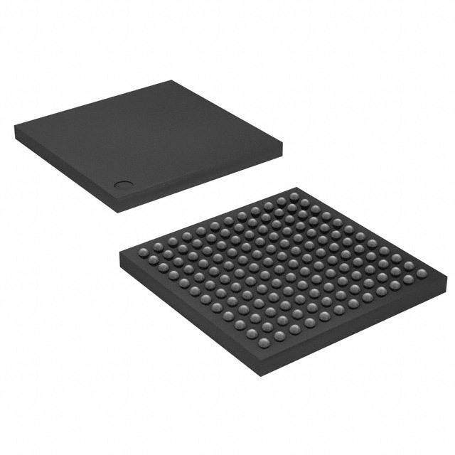
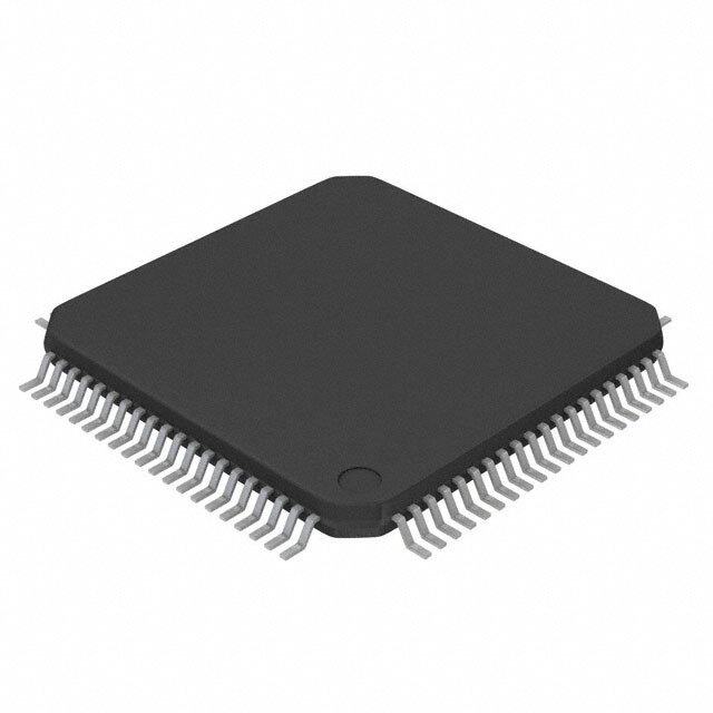
SAM7SE512/256/32 Summary 4. Package The SAM7SE512/256/32 is available in: (cid:129) 20 x 14 mm 128-lead LQFP package with a 0.5 mm lead pitch. (cid:129) 10x 10 x 1.4 mm 144-ball LFBGA package with a 0.8 mm lead pitch 4.1 128-lead LQFP Package Outline Figure 4-1 shows the orientation of the 128-lead LQFP package and a detailed mechanical description is given in the Mechanical Characteristics section of the full datasheet. Figure 4-1. 128-lead LQFP Package Outline (Top View) 102 65 103 64 128 39 1 38 9 6222GS–ATARM–6-Sep-11
4.2 128-lead LQFP Pinout Table 4-1. Pinout in 128-lead LQFP Package 1 ADVREF 33 PB31 65 TDI 97 SDCK 2 GND 34 PB30 66 TDO 98 PC8 3 AD7 35 PB29 67 PB2 99 PC7 4 AD6 36 PB28 68 PB1 100 PC6 5 AD5 37 PB27 69 PB0 101 PC5 6 AD4 38 PB26 70 GND 102 PC4 7 VDDOUT 39 PB25 71 VDDIO 103 PC3 8 VDDIN 40 PB24 72 VDDCORE 104 PC2 9 PA20/PGMD8/AD3 41 PB23 73 NRST 105 PC1 10 PA19/PGMD7/AD2 42 PB22 74 TST 106 PC0 11 PA18/PGMD6/AD1 43 PB21 75 ERASE 107 PA31 12 PA17/PGMD5/AD0 44 PB20 76 TCK 108 PA30 13 PA16/PGMD4 45 GND 77 TMS 109 PA29 14 PA15/PGMD3 46 VDDIO 78 JTAGSEL 110 PA28 15 PA14/PGMD2 47 VDDCORE 79 PC23 111 PA27/PGMD15 16 PA13/PGMD1 48 PB19 80 PC22 112 PA26/PGMD14 17 PA12/PGMD0 49 PB18 81 PC21 113 PA25/PGMD13 18 PA11/PGMM3 50 PB17 82 PC20 114 PA24/PGMD12 19 PA10/PGMM2 51 PB16 83 PC19 115 PA23/PGMD11 20 PA9/PGMM1 52 PB15 84 PC18 116 PA22/PGMD10 21 VDDIO 53 PB14 85 PC17 117 PA21/PGMD9 22 GND 54 PB13 86 PC16 118 VDDCORE 23 VDDCORE 55 PB12 87 PC15 119 GND 24 PA8/PGMM0 56 PB11 88 PC14 120 VDDIO 25 PA7/PGMNVALID 57 PB10 89 PC13 121 DM 26 PA6/PGMNOE 58 PB9 90 PC12 122 DP 27 PA5/PGMRDY 59 PB8 91 PC11 123 VDDFLASH 28 PA4/PGMNCMD 60 PB7 92 PC10 124 GND 29 PA3 61 PB6 93 PC9 125 XIN/PGMCK 30 PA2/PGMEN2 62 PB5 94 GND 126 XOUT 31 PA1/PGMEN1 63 PB4 95 VDDIO 127 PLLRC 32 PA0/PGMEN0 64 PB3 96 VDDCORE 128 VDDPLL SAM7SE512/256/32 Summary 10 6222GS–ATARM–6-Sep-11
SAM7SE512/256/32 Summary 4.3 144-ball LFBGA Package Outline Figure 4-2 shows the orientation of the 144-ball LFBGA package and a detailed mechanical description is given in the Mechanical Characteristics section. Figure 4-2. 144-ball LFBGA Package Outline (Top View) 12 11 10 9 8 7 6 5 4 3 2 1 A B C D E F G H J K L M Ball A1 11 6222GS–ATARM–6-Sep-11
4.4 144-ball LFBGA Pinout Table 4-2. SAM7SE512/256/32 Pinout for 144-ball LFBGA Package Pin Signal Name Pin Signal Name Pin Signal Name Pin Signal Name A1 PB7 D1 VDDCORE G1 PC18 K1 PC11 A2 PB8 D2 VDDCORE G2 PC16 K2 PC6 A3 PB9 D3 PB2 G3 PC17 K3 PC2 A4 PB12 D4 TDO G4 PC9 K4 PC0 A5 PB13 D5 TDI G5 VDDIO K5 PA27/PGMD15 A6 PB16 D6 PB17 G6 GND K6 PA26/PGMD14 A7 PB22 D7 PB26 G7 GND K7 GND A8 PB23 D8 PA14/PGMD2 G8 GND K8 VDDCORE A9 PB25 D9 PA12/PGMD0 G9 GND K9 VDDFLASH A10 PB29 D10 PA11/PGMM3 G10 AD4 K10 VDDIO A11 PB30 D11 PA8/PGMM0 G11 VDDIN K11 VDDIO A12 PB31 D12 PA7/PGMNVALID G12 VDDOUT K12 PA18/PGMD6/AD1 B1 PB6 E1 PC22 H1 PC15 L1 SDCK B2 PB3 E2 PC23 H2 PC14 L2 PC7 B3 PB4 E3 NRST H3 PC13 L3 PC4 B4 PB10 E4 TCK H4 VDDCORE L4 PC1 B5 PB14 E5 ERASE H5 VDDCORE L5 PA29 B6 PB18 E6 TEST H6 GND L6 PA24/PGMD12 B7 PB20 E7 VDDCORE H7 GND L7 PA21/PGMD9 B8 PB24 E8 VDDCORE H8 GND L8 ADVREF B9 PB28 E9 GND H9 GND L9 VDDFLASH B10 PA4/PGMNCMD E10 PA9/PGMM1 H10 PA19/PGMD7/AD2 L10 VDDFLASH B11 PA0/PGMEN0 E11 PA10/PGMM2 H11 PA20/PGMD8/AD3 L11 PA17/PGMD5/AD0 B12 PA1/PGMEN1 E12 PA13/PGMD1 H12 VDDIO L12 GND C1 PB0 F1 PC21 J1 PC12 M1 PC8 C2 PB1 F2 PC20 J2 PC10 M2 PC5 C3 PB5 F3 PC19 J3 PA30 M3 PC3 C4 PB11 F4 JTAGSEL J4 PA28 M4 PA31 C5 PB15 F5 TMS J5 PA23/PGMD11 M5 PA25/PGMD13 C6 PB19 F6 VDDIO J6 PA22/PGMD10 M6 DM C7 PB21 F7 GND J7 AD6 M7 DP C8 PB27 F8 GND J8 AD7 M8 GND C9 PA6/PGMNOE F9 GND J9 VDDCORE M9 XIN/PGMCK C10 PA5/PGMRDY F10 AD5 J10 VDDCORE M10 XOUT C11 PA2/PGMEN2 F11 PA15/PGMD3 J11 VDDCORE M11 PLLRC C12 PA3 F12 PA16/PGMD4 J12 VDDIO M12 VDDPLL SAM7SE512/256/32 Summary 12 6222GS–ATARM–6-Sep-11
SAM7SE512/256/32 Summary 5. Power Considerations 5.1 Power Supplies The SAM7SE512/256/32 has six types of power supply pins and integrates a voltage regulator, allowing the device to be supplied with only one voltage. The six power supply pin types are: (cid:129) VDDIN pin. It powers the voltage regulator and the ADC; voltage ranges from 3.0V to 3.6V, 3.3V nominal. (cid:129) VDDOUT pin. It is the output of the 1.8V voltage regulator. (cid:129) VDDIO pin. It powers the I/O lines; two voltage ranges are supported: – from 3.0V to 3.6V, 3.3V nominal – or from 1.65V to 1.95V, 1.8V nominal. (cid:129) VDDFLASH pin. It powers the USB transceivers and a part of the Flash. It is required for the Flash to operate correctly; voltage ranges from 3.0V to 3.6V, 3.3V nominal. (cid:129) VDDCORE pins. They power the logic of the device; voltage ranges from 1.65V to 1.95V, 1.8V typical. It can be connected to the VDDOUT pin with decoupling capacitor. VDDCORE is required for the device, including its embedded Flash, to operate correctly. (cid:129) VDDPLL pin. It powers the oscillator and the PLL. It can be connected directly to the VDDOUT pin. In order to decrease current consumption, if the voltage regulator and the ADC are not used, VDDIN, ADVREF, AD4, AD5, AD6 and AD7 should be connected to GND. In this case VDDOUT should be left unconnected. No separate ground pins are provided for the different power supplies. Only GND pins are pro- vided and should be connected as shortly as possible to the system ground plane. 5.2 Power Consumption The SAM7SE512/256/32 has a static current of less than 60 µA on VDDCORE at 25°C, includ- ing the RC oscillator, the voltage regulator and the power-on reset when the brownout detector is deactivated. Activating the brownout detector adds 20 µA static current. The dynamic power consumption on VDDCORE is less than 80 mA at full speed when running out of the Flash. Under the same conditions, the power consumption on VDDFLASH does not exceed 10 mA. 5.3 Voltage Regulator The SAM7SE512/256/32 embeds a voltage regulator that is managed by the System Controller. In Normal Mode, the voltage regulator consumes less than 100 µA static current and draws 100 mA of output current. The voltage regulator also has a Low-power Mode. In this mode, it consumes less than 20 µA static current and draws 1 mA of output current. Adequate output supply decoupling is mandatory for VDDOUT to reduce ripple and avoid oscil- lations. The best way to achieve this is to use two capacitors in parallel: (cid:129) One external 470 pF (or 1 nF) NPO capacitor should be connected between VDDOUT and GND as close to the chip as possible. 13 6222GS–ATARM–6-Sep-11
(cid:129) One external 2.2 µF (or 3.3 µF) X7R capacitor should be connected between VDDOUT and GND. Adequate input supply decoupling is mandatory for VDDIN in order to improve startup stability and reduce source voltage drop. The input decoupling capacitor should be placed close to the chip. For example, two capacitors can be used in parallel: 100 nF NPO and 4.7 µF X7R. 5.4 Typical Powering Schematics The SAM7SE512/256/32 supports a 3.3V single supply mode. The internal regulator input con- nected to the 3.3V source and its output feeds VDDCORE and the VDDPLL. Figure 5-1 shows the power schematics to be used for USB bus-powered systems. Figure 5-1. 3.3V System Single Power Supply Schematic VDDFLASH Power Source VDDIO ranges DC/DC Converter from 4.5V (USB) to 18V VDDIN 3.3V Voltage Regulator VDDOUT VDDCORE VDDPLL SAM7SE512/256/32 Summary 14 6222GS–ATARM–6-Sep-11
SAM7SE512/256/32 Summary 6. /O Lines Considerations 6.1 JTAG Port Pins TMS, TDI and TCK are Schmitt trigger inputs. TMS, TDI and TCK do not integrate a pull-up resistor. TDO is an output, driven at up to VDDIO, and has no pull-up resistor. The JTAGSEL pin is used to select the JTAG boundary scan when asserted at a high level. The JTAGSEL pin integrates a permanent pull-down resistor of about 15 kΩ. To eliminate any risk of spuriously entering the JTAG boundary scan mode due to noise on JTAGSEL, it should be tied externally to GND if boundary scan is not used, or put in place an external low value resistor (such as 1 kΩ). 6.2 Test Pin The TST pin is used for manufacturing test or fast programming mode of the SAM7SE512/256/32 when asserted high. The TST pin integrates a permanent pull-down resis- tor of about 15 kΩ to GND. To eliminate any risk of entering the test mode due to noise on the TST pin, it should be tied to GND if the FFPI is not used, or put in place an external low value resistor (such as 1 kΩ). To enter fast programming mode, the TST pin and the PA0 and PA1 pins should be tied high and PA2 tied low. Driving the TST pin at a high level while PA0 or PA1 is driven at 0 leads to unpredictable results. 6.3 Reset Pin The NRST pin is bidirectional with an open-drain output buffer. It is handled by the on-chip reset controller and can be driven low to provide a reset signal to the external components or asserted low externally to reset the microcontroller. There is no constraint on the length of the reset pulse, and the reset controller can guarantee a minimum pulse length. This allows connection of a sim- ple push-button on the NRST pin as system user reset, and the use of the NRST signal to reset all the components of the system. An external power-on reset can drive this pin during the start-up instead of using the internal power-on reset circuit. The NRST pin integrates a permanent pull-up of about 100 kΩ resistor to VDDIO. This pin has Schmitt trigger input. 6.4 ERASE Pin The ERASE pin is used to re-initialize the Flash content and some of its NVM bits. It integrates a permanent pull-down resistor of about 15 kΩ to GND. To eliminate any risk of erasing the Flash due to noise on the ERASE pin, it should be tied exter- nally to GND, which prevents erasing the Flash from the application, or put in place an external low value resistor (such as 1 kΩ). This pin is debounced by the RC oscillator to improve the glitch tolerance. When the pin is tied to high during less than 100 ms, ERASE pin is not taken into account. The pin must be tied high during more than 220 ms to perform the re-initialization of the Flash. 15 6222GS–ATARM–6-Sep-11
6.5 SDCK Pin The SDCK pin is dedicated to the SDRAM Clock and is an output-only without pull-up. Maximum Output Frequency of this pad is 48 MHz at 3.0V and 25 MHz at 1.65V with a maximum load of 30 pF. 6.6 PIO Controller lines All the I/O lines PA0 to PA31, PB0 to PB31, PC0 to PC23 integrate a programmable pull-up resistor. Programming of this pull-up resistor is performed independently for each I/O line through the PIO controllers. Typical pull-up value is 100 kΩ. All the I/O lines have schmitt trigger inputs. 6.7 I/O Lines Current Drawing The PIO lines PA0 to PA3 are high-drive current capable. Each of these I/O lines can drive up to 16 mA permanently. The remaining I/O lines can draw only 8 mA. However, the total current drawn by all the I/O lines cannot exceed 300 mA. SAM7SE512/256/32 Summary 16 6222GS–ATARM–6-Sep-11
SAM7SE512/256/32 Summary 7. Processor and Architecture 7.1 ARM7TDMI Processor (cid:129) RISC processor based on ARMv4T Von Neumann architecture – Runs at up to 55 MHz, providing 0.9 MIPS/MHz (core supplied with 1.8V) (cid:129) Two instruction sets – ARM® high-performance 32-bit instruction set – Thumb® high code density 16-bit instruction set (cid:129) Three-stage pipeline architecture – Instruction Fetch (F) – Instruction Decode (D) – Execute (E) 7.2 Debug and Test Features (cid:129) EmbeddedICE™ (Integrated embedded in-circuit emulator) – Two watchpoint units – Test access port accessible through a JTAG protocol – Debug communication channel (cid:129) Debug Unit – Two-pin UART – Debug communication channel interrupt handling – Chip ID Register (cid:129) IEEE1149.1 JTAG Boundary-scan on all digital pins 7.3 Memory Controller (cid:129) Programmable Bus Arbiter – Handles requests from the ARM7TDMI and the Peripheral DMA Controller (cid:129) Address decoder provides selection signals for – Four internal 1 Mbyte memory areas – One 256-Mbyte embedded peripheral area – Eight external 256-Mbyte memory areas (cid:129) Abort Status Registers – Source, Type and all parameters of the access leading to an abort are saved – Facilitates debug by detection of bad pointers (cid:129) Misalignment Detector – Alignment checking of all data accesses – Abort generation in case of misalignment (cid:129) Remap Command – Remaps the SRAM in place of the embedded non-volatile memory – Allows handling of dynamic exception vectors (cid:129) 16-area Memory Protection Unit (Internal Memory and peripheral protection only) 17 6222GS–ATARM–6-Sep-11
– Individually programmable size between 1K Byte and 1M Byte – Individually programmable protection against write and/or user access – Peripheral protection against write and/or user access (cid:129) Embedded Flash Controller – Embedded Flash interface, up to three programmable wait states – Prefetch buffer, buffering and anticipating the 16-bit requests, reducing the required wait states – Key-protected program, erase and lock/unlock sequencer – Single command for erasing, programming and locking operations – Interrupt generation in case of forbidden operation 7.4 External Bus Interface (cid:129) Integrates Three External Memory Controllers: – Static Memory Controller – SDRAM Controller – ECC Controller (cid:129) Additional Logic for NAND Flash and CompactFlash® Support – NAND Flash support: 8-bit as well as 16-bit devices are supported – CompactFlash support: all modes (Attribute Memory, Common Memory, I/O, True IDE) are supported but the signals _IOIS16 (I/O and True IDE modes) and -ATA SEL (True IDE mode) are not handled. (cid:129) Optimized External Bus: – 16- or 32-bit Data Bus (32-bit Data Bus for SDRAM only) – Up to 23-bit Address Bus, Up to 8-Mbytes Addressable – Up to 8 Chip Selects, each reserved to one of the eight Memory Areas – Optimized pin multiplexing to reduce latencies on External Memories (cid:129) Configurable Chip Select Assignment: – Static Memory Controller on NCS0 – SDRAM Controller or Static Memory Controller on NCS1 – Static Memory Controller on NCS2, Optional CompactFlash Support – Static Memory Controller on NCS3, NCS5 - NCS6, Optional NAND Flash Support – Static Memory Controller on NCS4, Optional CompactFlash Support – Static Memory Controller on NCS7 7.5 Static Memory Controller (cid:129) External memory mapping, 512-Mbyte address space (cid:129) 8-, or 16-bit Data Bus (cid:129) Up to 8 Chip Select Lines (cid:129) Multiple Access Modes supported – Byte Write or Byte Select Lines – Two different Read Protocols for each Memory Bank SAM7SE512/256/32 Summary 18 6222GS–ATARM–6-Sep-11
SAM7SE512/256/32 Summary (cid:129) Multiple device adaptability – Compliant with LCD Module – Compliant with PSRAM in synchronous operations – Programmable Setup Time Read/Write – Programmable Hold Time Read/Write (cid:129) Multiple Wait State Management – Programmable Wait State Generation – External Wait Request – Programmable Data Float Time 7.6 SDRAM Controller (cid:129) Numerous configurations supported – 2K, 4K, 8K Row Address Memory Parts – SDRAM with two or four Internal Banks – SDRAM with 16- or 32-bit Data Path (cid:129) Programming facilities – Word, half-word, byte access – Automatic page break when Memory Boundary has been reached – Multibank Ping-pong Access – Timing parameters specified by software – Automatic refresh operation, refresh rate is programmable (cid:129) Energy-saving capabilities – Self-refresh, and Low-power Modes supported (cid:129) Error detection – Refresh Error Interrupt (cid:129) SDRAM Power-up Initialization by software (cid:129) Latency is set to two clocks (CAS Latency of 1, 3 Not Supported) (cid:129) Auto Precharge Command not used (cid:129) Mobile SDRAM supported (except for low-power extended mode and deep power-down mode) 7.7 Error Corrected Code Controller (cid:129) Tracking the accesses to a NAND Flash device by triggering on the corresponding chip select (cid:129) Single bit error correction and 2-bit Random detection. (cid:129) Automatic Hamming Code Calculation while writing – ECC value available in a register (cid:129) Automatic Hamming Code Calculation while reading – Error Report, including error flag, correctable error flag and word address being detected erroneous – Supports 8- or 16-bit NAND Flash devices with 512-, 1024-, 2048- or 4096-byte pages 19 6222GS–ATARM–6-Sep-11
7.8 Peripheral DMA Controller (cid:129) Handles data transfer between peripherals and memories (cid:129) Eleven channels – Two for each USART – Two for the Debug Unit – Two for the Serial Synchronous Controller – Two for the Serial Peripheral Interface – One for the Analog-to-digital Converter (cid:129) Low bus arbitration overhead – One Master Clock cycle needed for a transfer from memory to peripheral – Two Master Clock cycles needed for a transfer from peripheral to memory (cid:129) Next Pointer management for reducing interrupt latency requirements (cid:129) Peripheral DMA Controller (PDC) priority is as follows (from the highest priority to the lowest): Receive DBGU Receive USART0 Receive USART1 Receive SSC Receive ADC Receive SPI Transmit DBGU Transmit USART0 Transmit USART1 Transmit SSC Transmit SPI SAM7SE512/256/32 Summary 20 6222GS–ATARM–6-Sep-11
SAM7SE512/256/32 Summary 8. Memories (cid:129) 512 Kbytes of Flash Memory (SAM7SE512) – dual plane – two contiguous banks of 1024 pages of 256 bytes – Fast access time, 30 MHz single-cycle access in Worst Case conditions – Page programming time: 6 ms, including page auto-erase – Page programming without auto-erase: 3 ms – Full chip erase time: 15 ms – 10,000 write cycles, 10-year data retention capability – 32 lock bits, each protecting 32 lock regions of 64 pages – Protection Mode to secure contents of the Flash (cid:129) 256 Kbytes of Flash Memory (SAM7SE256) – single plane – one bank of 1024 pages of 256 bytes – Fast access time, 30 MHz single-cycle access in Worst Case conditions – Page programming time: 6 ms, including page auto-erase – Page programming without auto-erase: 3 ms – Full chip erase time: 15 ms – 10,000 cycles, 10-year data retention capability – 16 lock bits, each protecting 16 lock regions of 64 pages – Protection Mode to secure contents of the Flash (cid:129) 32 Kbytes of Flash Memory (SAM7SE32) – single plane – one bank of 256 pages of 128 bytes – Fast access time, 30 MHz single-cycle access in Worst Case conditions – Page programming time: 6 ms, including page auto-erase – Page programming without auto-erase: 3 ms – Full chip erase time: 15 ms – 10,000 cycles, 10-year data retention capability – 8 lock bits, each protecting 8 lock regions of 32 pages – Protection Mode to secure contents of the Flash (cid:129) 32 Kbytes of Fast SRAM (SAM7SE512/256) – Single-cycle access at full speed (cid:129) 8 Kbytes of Fast SRAM (SAM7SE32) – Single-cycle access at full speed 21 6222GS–ATARM–6-Sep-11
Figure 8-1. SAM7SE Memory Mapping Address Memory Space Internal Memory Mapping Note: 0x0000 0000 (1) Can be ROM, Flash or SRAM 0x0000 0000 Boot Memory (1) depending on GPNVM2 and REMAP Internal Memories 256 MBytes Flash before Remap 1 MBytes SRAM after Remap 0x0FFF FFFF 0x000F FFFF 0x1000 0000 0x0010 0000 EBI Chip Select 0 256 MBytes Internal Flash 1 MBytes SMC 0x001F FFFF 0x1FFF FFFF 0x0020 0000 0x2000 0000 EBI Internal SRAM 1 MBytes Chip Select 1/ 256 MBytes 0x002F FFFF SMC or SDRAMC 0x0030 0000 0x2FFF FFFF 0x3000 0000 Internal ROM 1 MBytes EBI Chip Select 2 256 MBytes 0x003F FFFF 0x0040 0000 SMC 0x3FFF FFFF 0x4000 0000 EBI Chip Select 3 Reserved 252 MBytes 256 MBytes SMC/NANDFlash/ 0x4FFF FFFF SmartMedia System Controller Mapping 0x5000 0000 0x0FFF FFFF EBI 0xFFFF F000 Chip Select 4 256 MBytes SMC AIC 512 Bytes/128 registers 0x5FFF FFFF Compact Flash 0x6000 0000 EBI 0xFFFF F1FF Chip Select 5 256 MBytes 0xFFFF F200 SMC 0x6FFF FFFF Compact Flash DBGU 512 Bytes/128 registers 0x7000 0000 EBI 0xFFFF F3FF Chip Select 6 256 MBytes 0xFFFF F400 Peripheral Mapping 0x7FFF FFFF 0x8000 0000 0xF000 0000 PIOA 512 Bytes/128 registers RReesseerrvveedd EBI 256 MBytes 0xFFF9 FFFF 0xFFFF F5FF Chip Select 7 0xFFFA 0000 TC0, TC1, TC2 16 Kbytes 0xFFFF F600 00xx980F0F0F 0F0F0F0F 00xxFFFFFFAA 34F0F0F0 PIOB 512 Bytes/128 registers Reserved 0xFFFA FFFF 0xFFFB 0000 0xFFFF F7FF UDP 16 Kbytes 0xFFFF F800 0xFFFB 3FFF 0xFFFB 4000 Reserved PIOC 512 Bytes/128 registers 0xFFFB 7FFF 0xFFFB 8000 TWI 16 Kbytes 0xFFFF F9FF 0xFFFB BFFF 0xFFFF FA00 0xFFFB C000 Reserved Reserved 0xFFFB FFFF 0xFFFC 0000 USART0 16 Kbytes 0xFFFF FBFF 0xFFFC 3FFF 0xFFFF FC00 6 x 256 MBytes 0xFFFC 4000 PMC 256 Bytes/64 registers USART1 16 Kbytes Undefined 1,536 MBytes 0xFFFC 7FFF 0xFFFF FCFF (Abort) 0xFFFC 8000 RReesseerrvveedd 0xFFFF FD00 RSTC 16 Bytes/4 registers 0xFFFC BFFF 0xFFFF FD0F 0xFFFC C000 PWMC 16 Kbytes Reserved 0xFFFC FFFF 0xFFFD 0000 0xFFFF FD20 RReesseerrvveedd RTT 16 Bytes/4 registers 0xFFFF FC2F 0xFFFD 3FFF 0xFFFD 4000 0xFFFF FD30 SSC 16 Kbytes 0xFFFF FC3F PIT 16 Bytes/4 registers 0xFFFD 7FFF 0xFFFF FD40 0xFFFD 8000 ADC 16 Kbytes 0xFFFF FD4F WDT 16 Bytes/4 registers 0xFFFD BFFF 0xFFFD C000 RReesseerrvveedd Reserved 0xFFFD FFFF 0xFFFF FD60 0xFFFE 0000 VREG 4 Bytes/1 register SPI 16 Kbytes 0xFFFF FC6F 0xEFFF FFFF 0xFFFE 3FFF 0xFFFF FD70 0xF000 0000 0xFFFE 4000 Reserved Reserved 0xFFFF FEFF 0xFFFF EFFF 0xFFFF FF00 Internal Peripherals 256 MBytes 0xFFFF F000 MC 256 Bytes/64 registers SYSC 0xFFFF FFFF 0xFFFF FFFF 0xFFFF FFFF SAM7SE512/256/32 Summary 22 6222GS–ATARM–6-Sep-11
SAM7SE512/256/32 Summary A first level of address decoding is performed by the Memory Controller, i.e., by the implementa- tion of the Advanced System Bus (ASB) with additional features. Decoding splits the 4G bytes of address space into 16 areas of 256M bytes. The areas 1 to 8 are directed to the EBI that associates these areas to the external chip selects NC0 to NCS7. The area 0 is reserved for the addressing of the internal memories, and a second level of decoding provides 1M byte of internal memory area. The area 15 is reserved for the peripherals and pro- vides access to the Advanced Peripheral Bus (APB). Other areas are unused and performing an access within them provides an abort to the master requesting such an access. 8.1 Embedded Memories 8.1.1 Internal Memories 8.1.1.1 Internal SRAM The SAM7SE512/256 embeds a high-speed 32-Kbyte SRAM bank. The SAM7SE32 embeds a high-speed 8-Kbyte SRAM bank. After reset and until the Remap Command is performed, the SRAM is only accessible at address 0x0020 0000. After Remap, the SRAM also becomes avail- able at address 0x0. 8.1.1.2 Internal ROM The SAM7SE512/256/32 embeds an Internal ROM. At any time, the ROM is mapped at address 0x30 0000. The ROM contains the FFPI and the SAM-BA boot program. 8.1.1.3 Internal Flash (cid:129) The SAM7SE512 features two banks of 256 Kbytes of Flash. (cid:129) The SAM7SE256 features one bank of 256 Kbytes of Flash. (cid:129) The SAM7SE32 features one bank of 32 Kbytes of Flash. At any time, the Flash is mapped to address 0x0010 0000. A general purpose NVM (GPNVM) bit is used to boot either on the ROM (default) or from the Flash. This GPNVM bit can be cleared or set respectively through the commands “Clear General-pur- pose NVM Bit” and “Set General-purpose NVM Bit” of the EFC User Interface. Setting the GPNVM bit 2 selects the boot from the Flash, clearing it selects the boot from the ROM. Asserting ERASE clears the GPNVM bit 2 and thus selects the boot from the ROM by default. 23 6222GS–ATARM–6-Sep-11
Figure 8-2. Internal Memory Mapping with GPNVM Bit 2 = 0 (default) 0x0000 0000 ROM Before Remap 1 M Bytes 0x000F FFFF SRAM After Remap 0x0010 0000 Internal FLASH 1 M Bytes 0x001F FFFF 0x0020 0000 256M Bytes Internal SRAM 1 M Bytes 0x002F FFFF 0x0030 0000 Internal ROM 1 M Bytes 0x003F FFFF 0x0040 0000 252 M Bytes Undefined Areas (Abort) 0x0FFF FFFF Figure 8-3. Internal Memory Mapping with GPNVM Bit 2 = 1 0x0000 0000 Flash Before Remap 1 M Bytes 0x000F FFFF SRAM After Remap 0x0010 0000 Internal FLASH 1 M Bytes 0x001F FFFF 0x0020 0000 256M Bytes Internal SRAM 1 M Bytes 0x002F FFFF 0x0030 0000 Internal ROM 1 M Bytes 0x003F FFFF 0x0040 0000 252 M Bytes Undefined Areas (Abort) 0x0FFF FFFF 8.1.2 Embedded Flash 8.1.2.1 Flash Overview The Flash of the SAM7SE512 is organized in two banks (dual plane) of 1024 pages of 256 bytes. It reads as 131,072 32-bit words. The Flash of the SAM7SE256 is organized in 1024 pages (single plane) of 256 bytes. It reads as 65,536 32-bit words. The Flash of the SAM7SE32 is organized in 256 pages (single plane) of 128 bytes. It reads as 8192 32-bit words. The Flash of the SAM7SE32 contains a 128-byte write buffer, accessible through a 32-bit interface. The Flash of the SAM7SE512/256 contains a 256-byte write buffer, accessible through a 32-bit interface. SAM7SE512/256/32 Summary 24 6222GS–ATARM–6-Sep-11
SAM7SE512/256/32 Summary The Flash benefits from the integration of a power reset cell and from the brownout detector. This prevents code corruption during power supply changes, even in the worst conditions. 8.1.2.2 Embedded Flash Controller The Embedded Flash Controller (EFC) manages accesses performed by the masters of the sys- tem. It enables reading the Flash and writing the write buffer. It also contains a User Interface, mapped within the Memory Controller on the APB. The User Interface allows: (cid:129) programming of the access parameters of the Flash (number of wait states, timings, etc.) (cid:129) starting commands such as full erase, page erase, page program, NVM bit set, NVM bit clear, etc. (cid:129) getting the end status of the last command (cid:129) getting error status (cid:129) programming interrupts on the end of the last commands or on errors The Embedded Flash Controller also provides a dual 32-bit Prefetch Buffer that optimizes 16-bit access to the Flash. This is particularly efficient when the processor is running in Thumb mode. (cid:129) Two EFCs (EFC0 and EFC1) are embedded in the SAM7SE512 to control each plane of 256 KBytes. Dual plane organization allows concurrent Read and Program. (cid:129) One EFC (EFC0) is embedded in the SAM7SE256 to control the single plane 256 KBytes. (cid:129) One EFC (EFC0) is embedded in the SAM7SE32 to control the single plane 32 KBytes. 8.1.2.3 Lock Regions The SAM7SE512 Embedded Flash Controller manages 32 lock bits to protect 32 regions of the flash against inadvertent flash erasing or programming commands. The SAM7SE512 contains 32 lock regions and each lock region contains 64 pages of 256 bytes. Each lock region has a size of 16 Kbytes. The SAM7SE256 Embedded Flash Controller manages 16 lock bits to protect 16 regions of the flash against inadvertent flash erasing or programming commands. The SAM7SE256 contains 16 lock regions and each lock region contains 64 pages of 256 bytes. Each lock region has a size of 16 Kbytes. The SAM7SE32 Embedded Flash Controller manages 8 lock bits to protect 8 regions of the flash against inadvertent flash erasing or programming commands. The SAM7SE32 contains 8 lock regions and each lock region contains 32 pages of 128 bytes. Each lock region has a size of 4 Kbytes. If a locked-region’s erase or program command occurs, the command is aborted and the EFC triggers an interrupt. The 32 (SAM7SE512), 16 (SAM7SE256) or 8 (SAM7SE32) NVM bits are software programma- ble through the EFC User Interface. The command “Set Lock Bit” enables the protection. The command “Clear Lock Bit” unlocks the lock region. Asserting the ERASE pin clears the lock bits, thus unlocking the entire Flash. 8.1.2.4 Security Bit Feature The SAM7SE512/256/32 features a security bit, based on a specific NVM-bit. When the security is enabled, any access to the Flash, either through the ICE interface or through the Fast Flash Programming Interface, is forbidden. 25 6222GS–ATARM–6-Sep-11
The security bit can only be enabled through the Command “Set Security Bit” of the EFC User Interface. Disabling the security bit can only be achieved by asserting the ERASE pin at 1 and after a full flash erase is performed. When the security bit is deactivated, all accesses to the flash are permitted. It is important to note that the assertion of the ERASE pin should always be longer than 200 ms. As the ERASE pin integrates a permanent pull-down, it can be left unconnected during normal operation. However, it is safer to connect it directly to GND for the final application. 8.1.2.5 Non-volatile Brownout Detector Control Two general purpose NVM (GPNVM) bits are used for controlling the brownout detector (BOD), so that even after a power loss, the brownout detector operations remain in their state. These two GPNVM bits can be cleared or set respectively through the commands “Clear Gen- eral-purpose NVM Bit” and “Set General-purpose NVM Bit” of the EFC User Interface. (cid:129) GPNVM bit 0 is used as a brownout detector enable bit. Setting the GPNVM bit 0 enables the BOD, clearing it disables the BOD. Asserting ERASE clears the GPNVM bit 0 and thus disables the brownout detector by default. (cid:129) GPNVM bit 1 is used as a brownout reset enable signal for the reset controller. Setting the GPNVM bit 1 enables the brownout reset when a brownout is detected, Clearing the GPNVM bit 1 disables the brownout reset. Asserting ERASE disables the brownout reset by default. 8.1.2.6 Calibration Bits Sixteen NVM bits are used to calibrate the brownout detector and the voltage regulator. These bits are factory configured and cannot be changed by the user. The ERASE pin has no effect on the calibration bits. 8.1.3 Fast Flash Programming Interface The Fast Flash Programming Interface allows programming the device through either a serial JTAG interface or through a multiplexed fully-handshaked parallel port. It allows gang-program- ming with market-standard industrial programmers. The FFPI supports read, page program, page erase, full erase, lock, unlock and protect commands. The Fast Flash Programming Interface is enabled and the Fast Programming Mode is entered when the TST pin and the PA0 and PA1 pins are all tied high and PA2 tied to low. (cid:129) The Flash of the SAM7SE512 is organized in 2048 pages of 256 bytes (dual plane). It reads as 131,072 32-bit words. (cid:129) The Flash of the SAM7SE256 is organized in 1024 pages of 256 bytes (single plane). It reads as 65,536 32-bit words. (cid:129) The Flash of the SAM7SE32 is organized in 256 pages of 128 bytes (single plane). It reads as 32,768 32-bit words. (cid:129) The Flash of the SAM7SE512/256 contains a 256-byte write buffer, accessible through a 32- bit interface. (cid:129) The Flash of the SAM7SE32 contains a 128-byte write buffer, accessible through a 32-bit interface. SAM7SE512/256/32 Summary 26 6222GS–ATARM–6-Sep-11
SAM7SE512/256/32 Summary 8.1.4 SAM-BA® Boot The SAM-BA Boot is a default Boot Program which provides an easy way to program in-situ the on-chip Flash memory. The SAM-BA Boot Assistant supports serial communication via the DBGU or the USB Device Port. (cid:129) Communication via the DBGU supports a wide range of crystals from 3 to 20 MHz via software auto-detection. (cid:129) Communication via the USB Device Port is limited to an 18.432 MHz crystal. The SAM-BA Boot provides an interface with SAM-BA Graphic User Interface (GUI). The SAM-BA Boot is in ROM and is mapped in Flash at address 0x0 when GPNVM bit 2 is set to 0. 8.2 External Memories The external memories are accessed through the External Bus Interface. Refer to the memory map in Figure 8-1 on page 22. 27 6222GS–ATARM–6-Sep-11
9. System Controller The System Controller manages all vital blocks of the microcontroller: interrupts, clocks, power, time, debug and reset. The System Controller peripherals are all mapped to the highest 4 Kbytes of address space, between addresses 0xFFFF F000 and 0xFFFF FFFF. Figure 9-1 on page 29 shows the System Controller Block Diagram. Figure 8-1 on page 22 shows the mapping of the User Interface of the System Controller periph- erals. Note that the Memory Controller configuration user interface is also mapped within this address space. SAM7SE512/256/32 Summary 28 6222GS–ATARM–6-Sep-11
SAM7SE512/256/32 Summary Figure 9-1. System Controller Block Diagram System Controller jtag_nreset Boundary Scan TAP Controller nirq irq0-irq1 Advanced nfiq fiq Interrupt periph_irq[2..18] Controller proc_nreset ARM7TDMI PCK int pit_irq debug rtt_irq wdt_irq dbgu_irq pmc_irq power_on_reset rstc_irq force_ntrst MCK Debug dbgu_irq periph_nreset Unit force_ntrst dbgu_rxd dbgu_txd security_bit MCK Periodic debug Interval pit_irq periph_nreset Timer SLCK Real-Time flash_poe Embedded rtt_irq periph_nreset Timer flash_wrdis Flash SLCK cal debidulge WaTticmhedrog wdt_irq gpnvm[0..2] proc_nreset cgaplnvm[0] gpnvm[1] wWdDt_RfaPuRltOC MCK en flash_wrdis bod_rst_en Memory BOD proc_nreset Controller power_on_reset jtag_nreset Reset periph_nreset Controller proc_nreset Voltage POR flash_poe Regulator standby Mode Voltage NRST rstc_irq Controller Regulator cal SLCK RCOSC SLCK periph_clk[2..18] UDPCK pck[0-3] periph_clk[11] USB Device XIN OSC MAINCK ManPaogweemr ent PCK periph_nreset Port XOUT Controller UDPCK periph_irq[11] MCK usb_suspend PLLRC PLL PLLCK pmc_irq int periph_nreset idle periph_clk[4..18] usb_suspend periph_nreset Embedded Peripherals periph_nreset periph_irq{2-3] periph_clk[2-3] irq0-irq1 dbgu_rxd PIO fiq periph_irq[4..18] Controller dbgu_txd in PA0-PA31 out PB0-PB31 enable PC0-PC29 29 6222GS–ATARM–6-Sep-11
9.1 Reset Controller (cid:129) Based on one power-on reset cell and a double brownout detector (cid:129) Status of the last reset, either Power-up Reset, Software Reset, User Reset, Watchdog Reset, Brownout Reset (cid:129) Controls the internal resets and the NRST pin output (cid:129) Allows to shape a signal on the NRST line, guaranteeing that the length of the pulse meets any requirement. 9.1.1 Brownout Detector and Power On Reset The SAM7SE512/256/32 embeds one brownout detection circuit and a power-on reset cell. The power-on reset is supplied with and monitors VDDCORE. Both signals are provided to the Flash to prevent any code corruption during power-up or power- down sequences or if brownouts occur on the VDDCORE power supply. The power-on reset cell has a limited-accuracy threshold at around 1.5V. Its output remains low during power-up until VDDCORE goes over this voltage level. This signal goes to the reset con- troller and allows a full re-initialization of the device. The brownout detector monitors the VDDCORE and VDDFLASH levels during operation by comparing it to a fixed trigger level. It secures system operations in the most difficult environ- ments and prevents code corruption in case of brownout on the VDDCORE or VDDFLASH. When the brownout detector is enabled and VDDCORE decreases to a value below the trigger level (Vbot18-, defined as Vbot18 - hyst/2), the brownout output is immediately activated. When VDDCORE increases above the trigger level (Vbot18+, defined as Vbot18 + hyst/2), the reset is released. The brownout detector only detects a drop if the voltage on VDDCORE stays below the threshold voltage for longer than about 1µs. The VDDCORE threshold voltage has a hysteresis of about 50 mV, to ensure spike free brown- out detection. The typical value of the brownout detector threshold is 1.68V with an accuracy of ± 2% and is factory calibrated. When the brownout detector is enabled and VDDFLASH decreases to a value below the trigger level (Vbot33-, defined as Vbot33 - hyst/2), the brownout output is immediately activated. When VDDFLASH increases above the trigger level (Vbot33+, defined as Vbot33 + hyst/2), the reset is released. The brownout detector only detects a drop if the voltage on VDDCORE stays below the threshold voltage for longer than about 1µs. The VDDFLASH threshold voltage has a hysteresis of about 50 mV, to ensure spike free brown- out detection. The typical value of the brownout detector threshold is 2.80V with an accuracy of ± 3.5% and is factory calibrated. The brownout detector is low-power, as it consumes less than 20 µA static current. However, it can be deactivated to save its static current. In this case, it consumes less than 1µA. The deac- tivation is configured through the GPNVM bit 0 of the Flash. 9.2 Clock Generator The Clock Generator embeds one low-power RC Oscillator, one Main Oscillator and one PLL with the following characteristics: (cid:129) RC Oscillator ranges between 22 KHz and 42 KHz SAM7SE512/256/32 Summary 30 6222GS–ATARM–6-Sep-11
SAM7SE512/256/32 Summary (cid:129) Main Oscillator frequency ranges between 3 and 20 MHz (cid:129) Main Oscillator can be bypassed (cid:129) PLL output ranges between 80 and 220 MHz It provides SLCK, MAINCK and PLLCK. Figure 9-2. Clock Generator Block Diagram Clock Generator Embedded Slow Clock RC SLCK Oscillator XIN Main Main Clock Oscillator MAINCK XOUT PLL and PLL Clock Divider PLLCK PLLRC Status Control Power Management Controller 9.3 Power Management Controller The Power Management Controller uses the Clock Generator outputs to provide: (cid:129) the Processor Clock PCK (cid:129) the Master Clock MCK (cid:129) the USB Clock UDPCK (cid:129) all the peripheral clocks, independently controllable (cid:129) three programmable clock outputs The Master Clock (MCK) is programmable from a few hundred Hz to the maximum operating fre- quency of the device. The Processor Clock (PCK) switches off when entering processor idle mode, thus allowing reduced power consumption while waiting for an interrupt. 31 6222GS–ATARM–6-Sep-11
Figure 9-3. Power Management Controller Block Diagram Processor PCK Clock Controller Master Clock Controller int Idle Mode SLCK MPALINLCCKK /1P,/2re,/s4c,.a..le,/r64 MCK Peripherals periph_clk[2..14] Clock Controller ON/OFF Programmable Clock Controller SLCK MAINCK Prescaler pck[0..2] PLLCK /1,/2,/4,...,/64 USB Clock Controller usb_suspend ON/OFF Divider PLLCK UDPCK /1,/2,/4 9.4 Advanced Interrupt Controller (cid:129) Controls the interrupt lines (nIRQ and nFIQ) of an ARM Processor (cid:129) Individually maskable and vectored interrupt sources – Source 0 is reserved for the Fast Interrupt Input (FIQ) – Source 1 is reserved for system peripherals (RTT, PIT, EFC, PMC, DBGU, etc.) – Other sources control the peripheral interrupts or external interrupts – Programmable edge-triggered or level-sensitive internal sources – Programmable positive/negative edge-triggered or high/low level-sensitive external sources (cid:129) 8-level Priority Controller – Drives the normal interrupt nIRQ of the processor – Handles priority of the interrupt sources – Higher priority interrupts can be served during service of lower priority interrupt (cid:129) Vectoring – Optimizes interrupt service routine branch and execution – One 32-bit vector register per interrupt source – Interrupt vector register reads the corresponding current interrupt vector (cid:129) Protect Mode – Easy debugging by preventing automatic operations (cid:129) Fast Forcing – Permits redirecting any interrupt source on the fast interrupt (cid:129) General Interrupt Mask – Provides processor synchronization on events without triggering an interrupt SAM7SE512/256/32 Summary 32 6222GS–ATARM–6-Sep-11
SAM7SE512/256/32 Summary 9.5 Debug Unit (cid:129) Comprises: – One two-pin UART – One Interface for the Debug Communication Channel (DCC) support – One set of Chip ID Registers – One Interface providing ICE Access Prevention (cid:129) Two-pin UART – USART-compatible User Interface – Programmable Baud Rate Generator – Parity, Framing and Overrun Error – Automatic Echo, Local Loopback and Remote Loopback Channel Modes (cid:129) Debug Communication Channel Support – Offers visibility of COMMRX and COMMTX signals from the ARM Processor (cid:129) Chip ID Registers – Identification of the device revision, sizes of the embedded memories, set of peripherals – Chip ID is 0x272A 0A40 (VERSION 0) for SAM7SE512 – Chip ID is 0x272A 0940 (VERSION 0) for SAM7SE256 – Chip ID is 0x2728 0340 (VERSION 0) for SAM7SE32 9.6 Periodic Interval Timer (cid:129) 20-bit programmable counter plus 12-bit interval counter 9.7 Watchdog Timer (cid:129) 12-bit key-protected Programmable Counter running on prescaled SLCK (cid:129) Provides reset or interrupt signals to the system (cid:129) Counter may be stopped while the processor is in debug state or in idle mode 9.8 Real-time Timer (cid:129) 32-bit free-running counter with alarm running on prescaled SLCK (cid:129) Programmable 16-bit prescaler for SLCK accuracy compensation 9.9 PIO Controllers (cid:129) Three PIO Controllers. PIO A and B each control 32 I/O lines and PIO C controls 24 I/O lines. (cid:129) Fully programmable through set/clear registers (cid:129) Multiplexing of two peripheral functions per I/O line (cid:129) For each I/O line (whether assigned to a peripheral or used as general-purpose I/O) – Input change interrupt – Half a clock period glitch filter – Multi-drive option enables driving in open drain – Programmable pull-up on each I/O line – Pin data status register, supplies visibility of the level on the pin at any time 33 6222GS–ATARM–6-Sep-11
(cid:129) Synchronous output, provides Set and Clear of several I/O lines in a single write 9.10 Voltage Regulator Controller The purpose of this controller is to select the Power Mode of the Voltage Regulator between Normal Mode (bit 0 is cleared) or Standby Mode (bit 0 is set). SAM7SE512/256/32 Summary 34 6222GS–ATARM–6-Sep-11
SAM7SE512/256/32 Summary 10. Peripherals 10.1 User Interface The User Peripherals are mapped in the 256 MBytes of the address space between 0xF000 0000 and 0xFFFF EFFF. Each peripheral is allocated 16 Kbytes of address space. A complete memory map is presented in Figure 8-1 on page 22. 10.2 Peripheral Identifiers The SAM7SE512/256/32 embeds a wide range of peripherals. Table 10-1 defines the Peripheral Identifiers of the SAM7SE512/256/32. Unique peripheral identifiers are defined for both the Advanced Interrupt Controller and the Power Management Controller. Table 10-1. Peripheral Identifiers Peripheral Peripheral Peripheral External ID Mnemonic Name Interrupt 0 AIC Advanced Interrupt Controller FIQ 1 SYSC(1) 2 PIOA Parallel I/O Controller A 3 PIOB Parallel I/O Controller B 4 PIOC Parallel I/O Controller C 5 SPI Serial Peripheral Interface 0 6 US0 USART 0 7 US1 USART 1 8 SSC Synchronous Serial Controller 9 TWI Two-wire Interface 10 PWMC PWM Controller 11 UDP USB Device Port 12 TC0 Timer/Counter 0 13 TC1 Timer/Counter 1 14 TC2 Timer/Counter 2 15 ADC(1) Analog-to Digital Converter 16-28 reserved 29 AIC Advanced Interrupt Controller IRQ0 30 AIC Advanced Interrupt Controller IRQ1 Note: 1. Setting SYSC and ADC bits in the clock set/clear registers of the PMC has no effect. The Sys- tem Controller is continuously clocked. The ADC clock is automatically started for the first conversion. In Sleep Mode the ADC clock is automatically stopped after each conversion. 35 6222GS–ATARM–6-Sep-11
10.3 Peripheral Multiplexing on PIO Lines The SAM7SE512/256/32 features three PIO controllers, PIOA, PIOB and PIOC, that multiplex the I/O lines of the peripheral set. PIO Controller A and B control 32 lines; PIO Controller C controls 24 lines. Each line can be assigned to one of two peripheral functions, A or B. Some of them can also be multiplexed with the analog inputs of the ADC Controller. Table 10-2 on page 37 defines how the I/O lines of the peripherals A and B or the analog inputs are multiplexed on the PIO Controller A, B and C. The two columns “Function” and “Comments” have been inserted for the user’s own comments; they may be used to track how pins are defined in an application. Note that some peripheral functions that are output only may be duplicated in the table. At reset, all I/O lines are automatically configured as input with the programmable pull-up enabled, so that the device is maintained in a static state as soon as a reset is detected. SAM7SE512/256/32 Summary 36 6222GS–ATARM–6-Sep-11
SAM7SE512/256/32 Summary 10.4 PIO Controller A Multiplexing Table 10-2. Multiplexing on PIO Controller A PIO Controller A Application Usage I/O Line Peripheral A Peripheral B Comments Function Comments PA0 PWM0 A0/NBS0 High-Drive PA1 PWM1 A1/NBS2 High-Drive PA2 PWM2 A2 High-Drive PA3 TWD A3 High-Drive PA4 TWCK A4 PA5 RXD0 A5 PA6 TXD0 A6 PA7 RTS0 A7 PA8 CTS0 A8 PA9 DRXD A9 PA10 DTXD A10 PA11 NPCS0 A11 PA12 MISO A12 PA13 MOSI A13 PA14 SPCK A14 PA15 TF A15 PA16 TK A16/BA0 PA17 TD A17/BA1 AD0 PA18 RD NBS3/CFIOW AD1 PA19 RK NCS4/CFCS0 AD2 PA20 RF NCS2/CFCS1 AD3 PA21 RXD1 NCS6/CFCE2 PA22 TXD1 NCS5/CFCE1 PA23 SCK1 NWR1/NBS1/CFIOR PA24 RTS1 SDA10 PA25 CTS1 SDCKE PA26 DCD1 NCS1/SDCS PA27 DTR1 SDWE PA28 DSR1 CAS PA29 RI1 RAS PA30 IRQ1 D30 PA31 NPCS1 D31 37 6222GS–ATARM–6-Sep-11
10.5 PIO Controller B Multiplexing Table 10-3. Multiplexing on PIO Controller B PIO Controller B Application Usage I/O Line Peripheral A Peripheral B Comments Function Comments PB0 TIOA0 A0/NBS0 PB1 TIOB0 A1/NBS2 PB2 SCK0 A2 PB3 NPCS3 A3 PB4 TCLK0 A4 PB5 NPCS3 A5 PB6 PCK0 A6 PB7 PWM3 A7 PB8 ADTRG A8 PB9 NPCS1 A9 PB10 NPCS2 A10 PB11 PWM0 A11 PB12 PWM1 A12 PB13 PWM2 A13 PB14 PWM3 A14 PB15 TIOA1 A15 PB16 TIOB1 A16/BA0 PB17 PCK1 A17/BA1 PB18 PCK2 D16 PB19 FIQ D17 PB20 IRQ0 D18 PB21 PCK1 D19 PB22 NPCS3 D20 PB23 PWM0 D21 PB24 PWM1 D22 PB25 PWM2 D23 PB26 TIOA2 D24 PB27 TIOB2 D25 PB28 TCLK1 D26 PB29 TCLK2 D27 PB30 NPCS2 D28 PB31 PCK2 D29 SAM7SE512/256/32 Summary 38 6222GS–ATARM–6-Sep-11
SAM7SE512/256/32 Summary 10.6 PIO Controller C Multiplexing Multiplexing on PIO Controller C PIO Controller C Application Usage I/O Line Peripheral A Peripheral B Comments Function Comments PC0 D0 PC1 D1 PC2 D2 PC3 D3 PC4 D4 PC5 D5 PC6 D6 PC7 D7 PC8 D8 RTS1 PC9 D9 DTR1 PC10 D10 PCK0 PC11 D11 PCK1 PC12 D12 PCK2 PC13 D13 PC14 D14 NPCS1 PC15 D15 NCS3/NANDCS PC16 A18 NWAIT PC17 A19 NANDOE PC18 A20 NANDWE PC19 A21/NANDALE PC20 A22/REG/NANDCLE NCS7 PC21 NWR0/NWE/CFWE PC22 NRD/CFOE PC23 CFRNW NCS0 10.7 Serial Peripheral Interface (cid:129) Supports communication with external serial devices – Four chip selects with external decoder allow communication with up to 15 peripherals – Serial memories, such as DataFlash® and 3-wire EEPROMs – Serial peripherals, such as ADCs, DACs, LCD Controllers, CAN Controllers and Sensors – External co-processors (cid:129) Master or slave serial peripheral bus interface 39 6222GS–ATARM–6-Sep-11
– 8- to 16-bit programmable data length per chip select – Programmable phase and polarity per chip select – Programmable transfer delays per chip select, between consecutive transfers and between clock and data – Programmable delay between consecutive transfers – Selectable mode fault detection – Maximum frequency at up to Master Clock 10.8 Two Wire Interface (cid:129) Master, Multi-Master and Slave Mode Operation (cid:129) Compatibility with standard two-wire serial memories (cid:129) One, two or three bytes for slave address (cid:129) Sequential read/write operations (cid:129) Bit Rate: Up to 400 Kbit/s (cid:129) General Call Supported in Slave Mode 10.9 USART (cid:129) Programmable Baud Rate Generator (cid:129) 5- to 9-bit full-duplex synchronous or asynchronous serial communications – 1, 1.5 or 2 stop bits in Asynchronous Mode – 1 or 2 stop bits in Synchronous Mode – Parity generation and error detection – Framing error detection, overrun error detection – MSB or LSB first – Optional break generation and detection – By 8 or by 16 over-sampling receiver frequency – Hardware handshaking RTS - CTS – Modem Signals Management DTR-DSR-DCD-RI on USART1 – Receiver time-out and transmitter timeguard – Multi-drop Mode with address generation and detection (cid:129) RS485 with driver control signal (cid:129) ISO7816, T = 0 or T = 1 Protocols for interfacing with smart cards – NACK handling, error counter with repetition and iteration limit (cid:129) IrDA® modulation and demodulation – Communication at up to 115.2 Kbps (cid:129) Test Modes – Remote Loopback, Local Loopback, Automatic Echo 10.10 Serial Synchronous Controller (cid:129) Provides serial synchronous communication links used in audio and telecom applications (cid:129) Contains an independent receiver and transmitter and a common clock divider SAM7SE512/256/32 Summary 40 6222GS–ATARM–6-Sep-11
SAM7SE512/256/32 Summary (cid:129) Offers a configurable frame sync and data length (cid:129) Receiver and transmitter can be programmed to start automatically or on detection of different event on the frame sync signal (cid:129) Receiver and transmitter include a data signal, a clock signal and a frame synchronization signal 10.11 Timer Counter (cid:129) Three 16-bit Timer Counter Channels – Two output compare or one input capture per channel (cid:129) Wide range of functions including: – Frequency measurement – Event counting – Interval measurement – Pulse generation – Delay timing – Pulse Width Modulation – Up/down capabilities (cid:129) Each channel is user-configurable and contains: – Three external clock inputs – Five internal clock inputs, as defined in Table 10-4 Table 10-4. Timer Counter Clocks Assignment TC Clock input Clock TIMER_CLOCK1 MCK/2 TIMER_CLOCK2 MCK/8 TIMER_CLOCK3 MCK/32 TIMER_CLOCK4 MCK/128 TIMER_CLOCK5 MCK/1024 – Two multi-purpose input/output signals – Two global registers that act on all three TC channels 10.12 PWM Controller (cid:129) Four channels, one 16-bit counter per channel (cid:129) Common clock generator, providing thirteen different clocks – One Modulo n counter providing eleven clocks – Two independent linear dividers working on modulo n counter outputs (cid:129) Independent channel programming – Independent enable/disable commands – Independent clock selection – Independent period and duty cycle, with double buffering – Programmable selection of the output waveform polarity – Programmable center or left aligned output waveform 41 6222GS–ATARM–6-Sep-11
10.13 USB Device Port (cid:129) USB V2.0 full-speed compliant,12 Mbits per second. (cid:129) Embedded USB V2.0 full-speed transceiver (cid:129) Embedded 2688-byte dual-port RAM for endpoints (cid:129) Eight endpoints – Endpoint 0: 64bytes – Endpoint 1 and 2: 64 bytes ping-pong – Endpoint 3: 64 bytes – Endpoint 4 and 5: 512 bytes ping-pong – Endpoint 6 and 7: 64 bytes ping-pong – Ping-pong Mode (two memory banks) for Isochronous and bulk endpoints (cid:129) Suspend/resume logic (cid:129) Integrated Pull-up on DDP 10.14 Analog-to-Digital Converter (cid:129) 8-channel ADC (cid:129) 10-bit 384 Ksamples/sec. or 8-bit 583 Ksamples/sec. Successive Approximation Register ADC (cid:129) ±2 LSB Integral Non Linearity, ±1 LSB Differential Non Linearity (cid:129) Integrated 8-to-1 multiplexer, offering eight independent 3.3V analog inputs (cid:129) External voltage reference for better accuracy on low voltage inputs (cid:129) Individual enable and disable of each channel (cid:129) Multiple trigger sources – Hardware or software trigger – External trigger pin – Timer Counter 0 to 2 outputs TIOA0 to TIOA2 trigger (cid:129) Sleep Mode and conversion sequencer – Automatic wakeup on trigger and back to sleep mode after conversions of all enabled channels (cid:129) Each analog input shared with digital signals SAM7SE512/256/32 Summary 42 6222GS–ATARM–6-Sep-11
SAM7SE512/256/32 Summary 11. Package Drawings Figure 11-1. 128-lead LQFP Package Drawing 43 6222GS–ATARM–6-Sep-11
Figure 11-2. 144-ball LFBGA Package Drawing All dimensions are in mm SAM7SE512/256/32 Summary 44 6222GS–ATARM–6-Sep-11
SAM7SE512/256/32 Summary 12. Ordering Information Table 12-1. Ordering Information Temperature Ordering Code MRL Package Package Type Operating Range Industrial AT91SAM7SE512B-AU B LQFP128 Green (-40⋅ C to 85⋅ C) Industrial AT91SAM7SE256B-AU B LQFP128 Green (-40⋅ C to 85⋅ C) Industrial AT91SAM7SE32B-AU B LQFP128 Green (-40⋅ C to 85⋅ C) Industrial AT91SAM7SE512B-CU B LFBGA144 Green (-40⋅ C to 85⋅ C) Industrial AT91SAM7SE256B-CU B LFBGA144 Green (-40⋅ C to 85⋅ C) Industrial AT91SAM7SE32B-CU B LFBGA144 Green (-40⋅ C to 85⋅ C) Industrial AT91SAM7SE512-AU A LQFP128 Green (-40⋅ C to 85⋅ C) Industrial AT91SAM7SE256-AU A LQFP128 Green (-40⋅ C to 85⋅ C) Industrial AT91SAM7SE32-AU A LQFP128 Green (-40⋅ C to 85⋅ C) Industrial AT91SAM7SE512-CU A LFBGA144 Green (-40⋅ C to 85⋅ C) Industrial AT91SAM7SE256-CU A LFBGA144 Green (-40⋅ C to 85⋅ C) Industrial AT91SAM7SE32-CU A LFBGA144 Green (-40⋅ C to 85⋅ C) 45 6222GS–ATARM–6-Sep-11
Revision History Change Request Doc. Rev Comments Ref. First issue 6222AS Revised Memories with condensed mapping. #2709 Added Package Outlines and 144-ball LFBGA pin and ordering information. 6222BS Section 12. “Ordering Information” on page 45 ordering information code reference changed #3699 Section 6.1 ”JTAG Port Pins”, Section 6.3 ”Reset Pin”, Section 6.5 ”SDCK Pin”, removed statement: “not 5V #3826 tolerant” Section 7.6 ”SDRAM Controller”, Mobile SDRAM controller added to SDRAMC features INL and DNL updated in Section 10.14 ”Analog-to-Digital Converter” #4005 6222CS “Features” on page 2, Fully Static Operation; added, up to 55 MHz at 1.8V and 85°C worst case conditions #3924 Section 7.1 ”ARM7TDMI Processor”, Runs at up to 55 MHz, providing 0.9 MIPS/MHz (core supplied with 1.8V) Section 7.8 ”Peripheral DMA Controller” PDC priority list added #3833 Section 7.5 ”Static Memory Controller”, Multiple device adaptability includes: compliant w/PSRAM in review synchronous operations. Figure 8-1 ”SAM7SE Memory Mapping” Compact Flash not shown w/EBI Chip Select 5. Compact Flash is 4804 shown with EBI Chip Select 2. 6222DS Section 8.1.2.1 ”Flash Overview”, updated AT91SAM7SE32 ...”reads as 8192 32-bit words.” 4512 Section 6. ”/O Lines Considerations”, “JTAG Port Pins”, “Test Pin”, “Reset Pin”, “ERASE Pin” descriptions 5062 updated 6222ES Section 10.11 ”Timer Counter”, .....the TC has two output compare and one input capture per channel. 4209 Features: “Mode for General Purpose Two-wire UART Serial Communication” added to “Debug Unit (DBGU)”. 5846 Signal Description: 6222FS Table 3-1, “Signal Description List”, AD0-AD3 and AD4-AD7 comments reversed. 5271 System Controller: Figure 9-1 ”System Controller Block Diagram”, ‘periph_nreset’ changed into ‘power_on_reset’ for RTT. 5222 MRL B Ordering Codes added to Table 12-1, “Ordering Information” 7749 6222GS ‘Product Description’ changed to ‘AT91SAM ARM-based Flash MCU’ on the first page. ‘AT91SAM’ product prefix changed to ‘SAM’, except for Chip ID and ordering codes. rfo SAM7SE512/256/32 Summary 46 6222GS–ATARM–6-Sep-11
Headquarters International Atmel Corporation Atmel Asia Limited Atmel Munich GmbH Atmel Japan 2325 Orchard Parkway Unit 01-5 & 16, 19F Business Campus 9F, Tonetsu Shinkawa Bldg. San Jose, CA 95131 BEA Tower, Millennium City 5 Parkring 4 1-24-8 Shinkawa USA 418 Kwun Tong Road D-85748 Garching b. Munich Chuo-ku, Tokyo 104-0033 Tel: (+1) (408) 441-0311 Kwun Tong, Kowloon GERMANY JAPAN Fax: (+1) (408) 487-2600 HONG KONG Tel: (+49) 89-31970-0 Tel: (81) 3-3523-3551 Tel: (+852) 2245-6100 Fax: (+49) 89-3194621 Fax: (81) 3-3523-7581 Fax: (+852) 2722-1369 Product Contact Web Site Technical Support Sales Contacts www.atmel.com AT91SAM Support www.atmel.com/contacts/ www.atmel.com/AT91SAM Atmel techincal support Literature Requests www.atmel.com/literature Disclaimer: The information in this document is provided in connection with Atmel products. No license, express or implied, by estoppel or otherwise, to any intellectual property right is granted by this document or in connection with the sale of Atmel products. EXCEPT AS SET FORTH IN ATMEL’S TERMS AND CONDI- TIONS OF SALE LOCATED ON ATMEL’S WEB SITE, ATMEL ASSUMES NO LIABILITY WHATSOEVER AND DISCLAIMS ANY EXPRESS, IMPLIED OR STATUTORY WARRANTY RELATING TO ITS PRODUCTS INCLUDING, BUT NOT LIMITED TO, THE IMPLIED WARRANTY OF MERCHANTABILITY, FITNESS FOR A PARTICULAR PURPOSE, OR NON-INFRINGEMENT. IN NO EVENT SHALL ATMEL BE LIABLE FOR ANY DIRECT, INDIRECT, CONSEQUENTIAL, PUNITIVE, SPECIAL OR INCIDEN- TAL DAMAGES (INCLUDING, WITHOUT LIMITATION, DAMAGES FOR LOSS OF PROFITS, BUSINESS INTERRUPTION, OR LOSS OF INFORMATION) ARISING OUT OF THE USE OR INABILITY TO USE THIS DOCUMENT, EVEN IF ATMEL HAS BEEN ADVISED OF THE POSSIBILITY OF SUCH DAMAGES. Atmel makes no representations or warranties with respect to the accuracy or completeness of the contents of this document and reserves the right to make changes to specifica- tions and product descriptions at any time without notice. Atmel does not make any commitment to update the information contained herein. Unless specifically pro- vided otherwise, Atmel products are not suitable for, and shall not be used in, automotive applications. Atmel’s products are not intended, authorized, or warranted for use as components in applications intended to support or sustain life. © 2011 Atmel Corporation. All rights reserved. Atmel®, Atmel logo and combinations thereof, SAMBA®, DataFlash®and others are registered trademarks or trademarks of Atmel Corporation or its subsidiaries. ARM®, ARMPowered®logo, Cortex®, Thumb®-2 and others are registered trademarks or trademarks of ARM Ltd. Windows® and others are registered trademarks or trademarks of Microsoft Corporation in the US and/or other countries. Other terms and product names may be trademarks of others. 6222GS–ATARM–6-Sep-11