ICGOO在线商城 > 集成电路(IC) > 嵌入式 - 微控制器 > AT89C55WD-24AU
 Datasheet下载
- 型号: AT89C55WD-24AU
- 制造商: Atmel
- 库位|库存: xxxx|xxxx
- 要求:
| 数量阶梯 | 香港交货 | 国内含税 |
| +xxxx | $xxxx | ¥xxxx |
查看当月历史价格
查看今年历史价格
AT89C55WD-24AU产品简介:
ICGOO电子元器件商城为您提供AT89C55WD-24AU由Atmel设计生产,在icgoo商城现货销售,并且可以通过原厂、代理商等渠道进行代购。 AT89C55WD-24AU价格参考。AtmelAT89C55WD-24AU封装/规格:嵌入式 - 微控制器, 8051 微控制器 IC 89C 8-位 24MHz 20KB(20K x 8) 闪存 44-TQFP(10x10)。您可以下载AT89C55WD-24AU参考资料、Datasheet数据手册功能说明书,资料中有AT89C55WD-24AU 详细功能的应用电路图电压和使用方法及教程。
AT89C55WD-24AU 是由 Microchip Technology 提供的一款 8 位嵌入式微控制器,属于经典的 8051 系列架构。该型号具有 24KB 的闪存程序存储器、128 字节的 RAM 和多种外设接口,适用于需要高效控制和低功耗的应用场景。以下是其主要应用场景:

1. 工业自动化
   AT89C55WD-24AU 可用于工业控制设备中,例如 PLC(可编程逻辑控制器)、传感器数据采集系统和电机控制系统。其丰富的 I/O 接口和定时器资源能够满足工业现场对多任务处理的需求。

2. 家用电器
   在家电领域,这款微控制器可用于冰箱、洗衣机、空调等设备的主控板设计。它支持实时监控和调节温度、湿度或转速等功能,同时具备良好的抗干扰能力。

3. 消费电子
   该型号适合用作便携式电子产品的核心处理器,如电子玩具、遥控器、数字显示设备等。其低功耗特性有助于延长电池寿命。

4. 通信设备
   微控制器可以作为小型通信模块的核心组件,用于短距离无线通信、数据传输和协议解析等任务。

5. 医疗设备
   在一些基础医疗设备中,例如血压计、血糖仪或脉搏监测仪,AT89C55WD-24AU 能够提供稳定的数据处理能力和简单的用户界面控制。

6. 安防系统
   它可用于门禁系统、报警装置和视频监控中的辅助控制单元,执行信号检测、状态判断及反馈操作。

7. 教育与开发平台
   由于其经典架构和易用性,这款微控制器也广泛应用于教学实验和 DIY 项目中,帮助学生和开发者学习嵌入式系统的基础知识。

总结来说,AT89C55WD-24AU 凭借其高性能、低成本和广泛的兼容性,在众多嵌入式应用中表现出色,特别适合需要简单而可靠控制逻辑的场景。
| 参数 | 数值 |
| 产品目录 | 集成电路 (IC) |
| 描述 | IC MCU 8BIT 20KB FLASH 44TQFP |
| EEPROM容量 | - |
| 产品分类 | |
| I/O数 | 32 |
| 品牌 | Atmel |
| 数据手册 | |
| 产品图片 |
|
| 产品型号 | AT89C55WD-24AU |
| RAM容量 | 256 x 8 |
| rohs | 无铅 / 符合限制有害物质指令(RoHS)规范要求 |
| 产品系列 | 89C |
| 产品培训模块 | http://www.digikey.cn/PTM/IndividualPTM.page?site=cn&lang=zhs&ptm=24997http://www.digikey.cn/PTM/IndividualPTM.page?site=cn&lang=zhs&ptm=26162http://www.digikey.cn/PTM/IndividualPTM.page?site=cn&lang=zhs&ptm=26159http://www.digikey.cn/PTM/IndividualPTM.page?site=cn&lang=zhs&ptm=26180 |
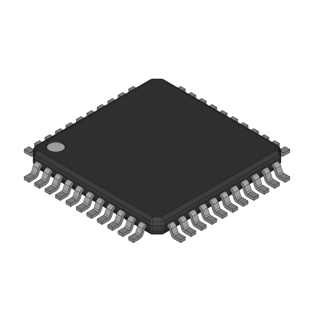
| 供应商器件封装 | 44-TQFP |
| 其它名称 | AT89C55WD24AU |
| 包装 | 托盘 |
| 外设 | WDT |
| 封装/外壳 | 44-TQFP |
| 工作温度 | -40°C ~ 85°C |
| 振荡器类型 | 内部 |
| 数据转换器 | - |
| 标准包装 | 160 |
| 核心处理器 | 8051 |
| 核心尺寸 | 8-位 |
| 电压-电源(Vcc/Vdd) | 4.5 V ~ 5.5 V |
| 程序存储器类型 | 闪存 |
| 程序存储容量 | 20KB(20K x 8) |
| 连接性 | UART/USART |
| 速度 | 24MHz |


PDF Datasheet 数据手册内容提取
Features • Compatible with MCS®-51 Products (cid:129) 20K Bytes of Reprogrammable Flash Memory (cid:129) Endurance: 10,000 Write/Erase Cycles (cid:129) 4V to 5.5V Operating Range (cid:129) Fully Static Operation: 0 Hz to 33 MHz (cid:129) Three-level Program Memory Lock (cid:129) 256 x 8-bit Internal RAM (cid:129) 32 Programmable I/O Lines 8-bit (cid:129) Three 16-bit Timer/Counters (cid:129) Eight Interrupt Sources Microcontroller (cid:129) Programmable Serial Channel (cid:129) Low-power Idle and Power-down Modes with 20K Bytes (cid:129) Interrupt Recovery from Power-down Mode (cid:129) Hardware Watchdog Timer Flash (cid:129) Dual Data Pointer (cid:129) Power-off Flag (cid:129) Green (Pb/Halide-free) Packaging Option AT89C55WD 1. Description The AT89C55WD is a low-power, high-performance CMOS 8-bit microcontroller with 20K bytes of Flash programmable read only memory and 256 bytes of RAM. The device is manufactured using Atmel’s high-density nonvolatile memory technology and is compatible with the industry standard 80C51 and 80C52 instruction set and pinout. The on-chip Flash allows the program memory to be user programmed by a conventional nonvolatile memory programmer. By combining a versatile 8-bit CPU with Flash on a monolithic chip, the Atmel AT89C55WD is a powerful microcomputer which provides a highly flexible and cost effective solution to many embedded control applications. The AT89C55WD provides the following standard features: 20K bytes of Flash, 256 bytes of RAM, 32 I/O lines, three 16-bit timer/counters, a six-vector, two-level interrupt architecture, a full-duplex serial port, on-chip oscillator, and clock circuitry. In addition, the AT89C55WD is designed with static logic for operation down to zero frequency and supports two software selectable power saving modes. The Idle Mode stops the CPU while allowing the RAM, timer/counters, serial port, and interrupt system to con- tinue functioning. The Power-down Mode saves the RAM contents but freezes the oscillator, disabling all other chip functions until the next external interrupt or hardware reset. 1921D–MICRO–6/08
2. Pin Configurations 2.1 44A – 44-lead TQFP P1.4P1.3P1.2P1.1 (T2 EX)P1.0 (T2)NCVCCP0.0 (AD0)P0.1 (AD1)P0.2 (AD2)P0.3 (AD3) 4443424140393837363534 P1.5 1 33 P0.4 (AD4) P1.6 2 32 P0.5 (AD5) P1.7 3 31 P0.6 (AD6) RST 4 30 P0.7 (AD7) (RXD) P3.0 5 29 EA/VPP NC 6 28 NC (TXD) P3.1 7 27 ALE/PROG (INT0) P3.2 8 26 PSEN (INT1) P3.3 9 25 P2.7 (A15) (T0) P3.4 10 24 P2.6 (A14) (T1) P3.5 11 23 P2.5 (A13) 1213141516171819202122 (WR) P3.6(RD) P3.7XTAL2XTAL1GNDGND(A8) P2.0(A9) P2.1(A10) P2.2(A11) P2.3(A12) P2.4 2.2 44J – 44-lead PLCC T2 EX)T2) AD0)AD1)AD2)AD3) 4321 (0 ( C0 (1 (2 (3 ( P1.P1.P1.P1.P1.NCVCP0.P0.P0.P0. 65432143210 P1.5 7 4444439 P0.4 (AD4) P1.6 8 38 P0.5 (AD5) P1.7 9 37 P0.6 (AD6) RST 10 36 P0.7 (AD7) (RXD) P3.0 11 35 EA/VPP NC 12 34 NC (TXD) P3.1 13 33 ALE/PROG (INT0) P3.2 14 32 PSEN (INT1) P3.3 15 31 P2.7 (A15) (T0) P3.4 16 30 P2.6 (A14) (T1) P3.5 17 29 P2.5 (A13) 89012345678 11222222222 6721DC01234 R) P3.D) P3.XTALXTALGNN8) P2.9) P2.0) P2.1) P2.2) P2. (W(R (A(A(A1(A1(A1 2.3 40P6 – 40-lead PDIP (T2) P1.0 1 40 VCC (T2EX) P1.1 2 39 P0.0 (AD0) P1.2 3 38 P0.1 (AD1) P1.3 4 37 P0.2 (AD2) P1.4 5 36 P0.3 (AD3) P1.5 6 35 P0.4 (AD4) P1.6 7 34 P0.5 (AD5) P1.7 8 33 P0.6 (AD6) RST 9 32 P0.7 (AD7) (RXD) P3.0 10 31 EA/VPP (TXD) P3.1 11 30 ALE/PROG (INT0) P3.2 12 29 PSEN (INT1) P3.3 13 28 P2.7 (A15) (T0) P3.4 14 27 P2.6 (A14) (T1) P3.5 15 26 P2.5 (A13) (WR) P3.6 16 25 P2.4 (A12) (RD) P3.7 17 24 P2.3 (A11) XTAL2 18 23 P2.2 (A10) XTAL1 19 22 P2.1 (A9) GND 20 21 P2.0 (A8) AT89C55WD 2 1921D–MICRO–6/08
AT89C55WD 3. Block Diagram P0.0 - P0.7 P2.0 - P2.7 V CC PORT 0 DRIVERS PORT 2 DRIVERS GND RAM ADDR. PORT 0 PORT 2 QUICK REGISTER RAM LATCH LATCH FLASH PROGRAM REGIBSTER ACC PSOTINACTEKR RAEDGDIRSETSESR BUFFER TMP2 TMP1 PC ALU INCREMENTER INTERRUPT, SERIAL PORT, AND TIMER BLOCKS PROGRAM PSW COUNTER PSEN ALE/PROG TIAMNINDG INSTRUCTION DUAL EA / V CONTROL REGISTER DPTR PP RST PORT 1 PORT 3 LATCH LATCH WATCH DOG OSC PORT 1 DRIVERS PORT 3 DRIVERS P1.0 - P1.7 P3.0 - P3.7 3 1921D–MICRO–6/08
4. Pin Description 4.1 VCC Supply voltage. 4.2 GND Ground. 4.3 Port 0 Port 0 is an 8-bit open drain bi-directional I/O port. As an output port, each pin can sink eight TTL inputs. When 1s are written to port 0 pins, the pins can be used as high-impedance inputs. Port 0 can also be configured to be the multiplexed low-order address/data bus during accesses to external program and data memory. In this mode, P0 has internal pull-ups. Port 0 also receives the code bytes during Flash programming and outputs the code bytes dur- ing program verification. External pull-ups are required during program verification. 4.4 Port 1 Port 1 is an 8-bit bi-directional I/O port with internal pull-ups. The Port 1 output buffers can sink/source four TTL inputs. When 1s are written to Port 1 pins, they are pulled high by the inter- nal pull-ups and can be used as inputs. As inputs, Port 1 pins that are externally being pulled low will source current (I ) because of the internal pull-ups. IL In addition, P1.0 and P1.1 can be configured to be the timer/counter 2 external count input (P1.0/T2) and the timer/counter 2 trigger input (P1.1/T2EX), respectively, as shown in the follow- ing table. Port 1 also receives the low-order address bytes during Flash programming and verification. Port Pin Alternate Functions P1.0 T2 (external count input to Timer/Counter 2), clock-out P1.1 T2EX (Timer/Counter 2 capture/reload trigger and direction control) 4.5 Port 2 Port 2 is an 8-bit bi-directional I/O port with internal pull-ups. The Port 2 output buffers can sink/source four TTL inputs. When 1s are written to Port 2 pins, they are pulled high by the inter- nal pull-ups and can be used as inputs. As inputs, Port 2 pins that are externally being pulled low will source current (I ) because of the internal pull-ups. IL Port 2 emits the high-order address byte during fetches from external program memory and dur- ing accesses to external data memory that use 16-bit addresses (MOVX @ DPTR). In this application, Port 2 uses strong internal pull-ups when emitting 1s. During accesses to external data memory that use 8-bit addresses (MOVX @ RI), Port 2 emits the contents of the P2 Special Function Register. Port 2 also receives the high-order address bits and some control signals during Flash program- ming and verification. AT89C55WD 4 1921D–MICRO–6/08
AT89C55WD 4.6 Port 3 Port 3 is an 8-bit bi-directional I/O port with internal pull-ups. The Port 3 output buffers can sink/source four TTL inputs. When 1s are written to Port 3 pins, they are pulled high by the inter- nal pull-ups and can be used as inputs. As inputs, Port 3 pins that are externally being pulled low will source current (I ) because of the pull-ups. IL Port 3 receives some control signals for Flash programming and verification. Port 3 also serves the functions of various special features of the AT89C55WD, as shown in the following table. Port Pin Alternate Functions P3.0 RXD (serial input port) P3.1 TXD (serial output port) P3.2 INT0 (external interrupt 0) P3.3 INT1 (external interrupt 1) P3.4 T0 (timer 0 external input) P3.5 T1 (timer 1 external input) P3.6 WR (external data memory write strobe) P3.7 RD (external data memory read strobe) 4.7 RST Reset input. A high on this pin for two machine cycles while the oscillator is running resets the device. This pin drives High for 98 oscillator periods after the Watchdog times out. The DISRTO bit in SFR AUXR (address 8EH) can be used to disable this feature. In the default state of bit DISRTO, the RESET HIGH out feature is enabled. 4.8 ALE/PROG Address Latch Enable is an output pulse for latching the low byte of the address during accesses to external memory. This pin is also the program pulse input (PROG) during Flash programming. In normal operation, ALE is emitted at a constant rate of 1/6 the oscillator frequency and may be used for external timing or clocking purposes. Note, however, that one ALE pulse is skipped dur- ing each access to external data memory. If desired, ALE operation can be disabled by setting bit 0 of SFR location 8EH. With the bit set, ALE is active only during a MOVX or MOVC instruction. Otherwise, the pin is weakly pulled high. Setting the ALE-disable bit has no effect if the microcontroller is in external execution mode. 4.9 PSEN Program Store Enable is the read strobe to external program memory. When the AT89C55WD is executing code from external program memory, PSEN is activated twice each machine cycle, except that two PSEN activations are skipped during each access to external data memory. 5 1921D–MICRO–6/08
4.10 EA/VPP External Access Enable. EA must be strapped to GND in order to enable the device to fetch code from external program memory locations starting at 0000H up to FFFFH. Note, however, that if lock bit 1 is programmed, EA will be internally latched on reset. EA should be strapped to V for internal program executions. CC This pin also receives the 12V programming enable voltage (V ) during Flash programming. PP 4.11 XTAL1 Input to the inverting oscillator amplifier and input to the internal clock operating circuit. 4.12 XTAL2 Output from the inverting oscillator amplifier. 5. Special Function Registers A map of the on-chip memory area called the Special Function Register (SFR) space is shown in Table 5-1. Table 5-1. AT89C55WD SFR Map and Reset Values 0F8H 0FFH B 0F0H 0F7H 00000000 0E8H 0EFH ACC 0E0H 0E7H 00000000 0D8H 0DFH PSW 0D0H 0D7H 00000000 T2CON T2MOD RCAP2L RCAP2H TL2 TH2 0C8H 0CFH 00000000 XXXXXX00 00000000 00000000 00000000 00000000 0C0H 0C7H IP 0B8H 0BFH XX000000 P3 0B0H 0B7H 11111111 IE 0A8H 0AFH 0X000000 P2 AUXR1 WDTRST 0A0H 0A7H 11111111 XXXXXXX0 XXXXXXXX SCON SBUF 98H 9FH 00000000 XXXXXXXX P1 90H 97H 11111111 TCON TMOD TL0 TL1 TH0 TH1 AUXR 88H 8FH 00000000 00000000 00000000 00000000 00000000 00000000 XXX00XX0 P0 SP DP0L DP0H DP1L DP1H PCON 80H 87H 11111111 00000111 00000000 00000000 00000000 00000000 0XXX0000 AT89C55WD 6 1921D–MICRO–6/08
AT89C55WD Note that not all of the addresses are occupied, and unoccupied addresses may not be imple- mented on the chip. Read accesses to these addresses will in general return random data, and write accesses will have an indeterminate effect. User software should not write 1s to these unlisted locations, since they may be used in future products to invoke new features. In that case, the reset or inactive values of the new bits will always be 0. Timer 2 Registers: Control and status bits are contained in registers T2CON (shown in Table 5- 2) and T2MOD (shown in Table 5-2) for Timer 2. The register pair (RCAP2H, RCAP2L) are the Capture/Reload registers for Timer 2 in 16-bit capture mode or 16-bit auto-reload mode. Interrupt Registers: The individual interrupt enable bits are in the IE register. Two priorities can be set for each of the six interrupt sources in the IP register. Dual Data Pointer Registers: To facilitate accessing both internal and external data memory, two banks of 16-bit Data Pointer Registers are provided: DP0 at SFR address locations 82H- 83H and DP1 at 84H-85H. Bit DPS = 0 in SFR AUXR1 selects DP0 and DPS = 1 selects DP1. The user should always initialize the DPS bit to the appropriate value before accessing the respective Data Pointer Register. Power Off Flag: The Power Off Flag (POF) is located at bit 4 (PCON.4) in the PCON SFR. POF is set to “1” during power up. It can be set and reset under software control and is not affected by reset. Table 5-2. T2CON—Timer/Counter 2 Control Register T2CON Address = 0C8H Reset Value = 0000 0000B Bit Addressable TF2 EXF2 RCLK TCLK EXEN2 TR2 C/T2 CP/RL2 Bit 7 6 5 4 3 2 1 0 Symbol Function Timer 2 overflow flag set by a Timer 2 overflow and must be cleared by software. TF2 will not be set when either RCLK TF2 = 1 or TCLK = 1. Timer 2 external flag set when either a capture or reload is caused by a negative transition on T2EX and EXEN2 = 1. EXF2 When Timer 2 interrupt is enabled, EXF2 = 1 will cause the CPU to vector to the Timer 2 interrupt routine. EXF2 must be cleared by software. EXF2 does not cause an interrupt in up/down counter mode (DCEN = 1). Receive clock enable. When set, causes the serial port to use Timer 2 overflow pulses for its receive clock in serial port RCLK Modes 1 and 3. RCLK = 0 causes Timer 1 overflow to be used for the receive clock. Transmit clock enable. When set, causes the serial port to use Timer 2 overflow pulses for its transmit clock in serial port TCLK Modes 1 and 3. TCLK = 0 causes Timer 1 overflows to be used for the transmit clock. Timer 2 external enable. When set, allows a capture or reload to occur as a result of a negative transition on T2EX if EXEN2 Timer 2 is not being used to clock the serial port. EXEN2 = 0 causes Timer 2 to ignore events at T2EX. TR2 Start/Stop control for Timer 2. TR2 = 1 starts the timer. Timer or counter select for Timer 2. C/T2 = 0 for timer function. C/T2 = 1 for external event counter (falling edge C/T2 triggered). Capture/Reload select. CP/RL2 = 1 causes captures to occur on negative transitions at T2EX if EXEN2 = 1. CP/RL2 = 0 CP/RL2 causes automatic reloads to occur when Timer 2 overflows or negative transitions occur at T2EX when EXEN2 = 1. When either RCLK or TCLK = 1, this bit is ignored and the timer is forced to auto-reload on Timer 2 overflow. 7 1921D–MICRO–6/08
Table 5-3. AUXR: Auxiliary Register AUXR Address = 8EH Reset Value = XXX00XX0B Not Bit Addressable – – – WDIDLE DISRTO – – DISALE Bit 7 6 5 4 3 2 1 0 – Reserved for future expansion DISALE Disable/Enable ALE DISALE Operating Mode 0 ALE is emitted at a constant rate of 1/6 the oscillator frequency 1 ALE is active only during a MOVX or MOVC instruction DISRTO Disable/Enable Reset out DISRTO Operating Mode 0 Reset pin is driven High after WDT times out 1 Reset pin is input only WDIDLE Disable/Enable WDT in IDLE mode WDIDLE Operating Mode 0 WDT continues to count in IDLE mode 1 WDT halts counting in IDLE mode Table 5-4. AUXR1: Auxiliary Register 1 AUXR1 Address = A2H Reset Value = XXXXXXX0B Not Bit Addressable – – – – – – – DPS Bit 7 6 5 4 3 2 1 0 – Reserved for future expansion DPS Data Pointer Register Select DPS 0 Selects DPTR Registers DP0L, DP0H 1 Selects DPTR Registers DP1L, DP1H AT89C55WD 8 1921D–MICRO–6/08
AT89C55WD 6. Memory Organization The MCS-51 devices have a separate address space for Program and Data Memory. Up to 64 Kbytes each of external Program and Data Memory can be addressed. 6.1 Program Memory If the EA pin is connected to GND, all program fetches are directed to external memory. On the AT89C55WD, if EA is connected to V , program fetches to addresses 0000H through CC 4FFFH are directed to internal memory and fetches to addresses 5000H through FFFFH are to external memory. 6.2 Data Memory The AT89C55WD implements 256 bytes of on-chip RAM. The upper 128 bytes occupy a parallel address space to the Special Function Registers. That means the upper 128 bytes have the same addresses as the SFR space but are physically separate from SFR space. When an instruction accesses an internal location above address 7FH, the address mode used in the instruction specifies whether the CPU accesses the upper 128 bytes of RAM or the SFR space. Instructions that use direct addressing access SFR space. For example, the following direct addressing instruction accesses the SFR at location 0A0H (which is P2). MOV 0A0H, #data Instructions that use indirect addressing access the upper 128 bytes of RAM. For example, the following indirect addressing instruction, where R0 contains 0A0H, accesses the data byte at address 0A0H, rather than P2 (whose address is 0A0H). MOV @R0, #data Note that stack operations are examples of indirect addressing, so the upper 128 bytes of data RAM are available as stack space. 7. Hardware Watchdog Timer (One-time Enabled with Reset-out) The WDT is intended as a recovery method in situations where the CPU may be subjected to software upsets. The WDT consists of a 13-bit counter and the WatchDog Timer Reset (WDTRST) SFR. The WDT is defaulted to disable from exiting reset. To enable the WDT, a user must write 01EH and 0E1H in sequence to the WDTRST register (SFR location 0A6H). When the WDT is enabled, it will increment every machine cycle while the oscillator is running. The WDT time-out period is dependent on the external clock frequency. There is no way to disable the WDT except through reset (either hardware reset or WDT overflow reset). When WDT over- flows, it will drive an output RESET HIGH pulse at the RST pin. 9 1921D–MICRO–6/08
8. Using the WDT To enable the WDT, a user must write 01EH and 0E1H in sequence to the WDTRST register (SFR location 0A6H). When the WDT is enabled, the user needs to service it by writing 01EH and 0E1H to WDTRST to avoid a WDT overflow. The 13-bit counter overflows when it reaches 8191 (1FFFH), and this will reset the device. When the WDT is enabled, it will increment every machine cycle while the oscillator is running. This means the user must re-initialize the WDT at least every 8191 machine cycles. To re-initialize the WDT the user must write 01EH and 0E1H to WDTRST. WDTRST is a write-only register. The WDT counter cannot be read or written. When WDT overflows, it will generate an output RESET pulse at the RST pin. The RESET pulse duration is 98xTOSC, where TOSC=1/FOSC. To make the best use of the WDT, it should be serviced in those sections of code that will periodically be executed within the time required to prevent a WDT reset. 9. WDT During Power-down and Idle In Power-down mode the oscillator stops, which means the WDT also stops. While in Power- down mode, the user does not need to service the WDT. There are two methods of exiting Power-down mode: by a hardware reset or via a level-activated external interrupt which is enabled prior to entering Power-down mode. When Power-down is exited with hardware reset, servicing the WDT should occur as it normally does whenever the AT89C55WD is reset. Exiting Power-down with an interrupt is significantly different. The interrupt is held low long enough for the oscillator to stabilize. When the interrupt is brought high, the interrupt is serviced. To prevent the WDT from resetting the device while the interrupt pin is held low, the WDT is not started until the interrupt is pulled high. It is suggested that the WDT be reset during the interrupt service for the interrupt used to exit Power-down. To ensure that the WDT does not overflow within a few states of exiting Power-down, it is best to reset the WDT just before entering Power-down. Before going into the IDLE mode, the WDIDLE bit in SFR AUXR is used to determine whether the WDT continues to count if enabled. The WDT keeps counting during IDLE (WDIDLE bit = 0) as the default state. To prevent the WDT from resetting the AT89C55WD while in IDLE mode, the user should always set up a timer that will periodically exit IDLE, service the WDT, and reen- ter IDLE mode. With WDIDLE bit enabled, the WDT will stop to count in IDLE mode and resumes the count upon exit from IDLE. 10. UART The UART in the AT89C55WD operates the same way as the UART in the AT89C51 and AT89C52. For more detailed information on the UART operation, please click on the document link below: http://www.atmel.com/dyn/resources/prod_documents/DOC4316.PDF 11. Timer 0 and 1 Timer 0 and Timer 1 in the AT89C55WD operate the same way as Timer 0 and Timer 1 in the AT89C51 and AT89C52. For further information on the timers’ operation, please click on the document link below: http://www.atmel.com/dyn/resources/prod_documents/DOC4316.PDF AT89C55WD 10 1921D–MICRO–6/08
AT89C55WD 12. Timer 2 Timer 2 is a 16-bit Timer/Counter that can operate as either a timer or an event counter. The type of operation is selected by bit C/T2 in the SFR T2CON (shown in Table 5-2). Timer 2 has three operating modes: capture, auto-reload (up or down counting), and baud rate generator. The modes are selected by bits in T2CON, as shown in Table 5-2. Timer 2 consists of two 8-bit registers, TH2 and TL2. In the Timer function, the TL2 register is incremented every machine cycle. Since a machine cycle consists of 12 oscillator periods, the count rate is 1/12 of the oscillator frequency. Table 12-1. Timer 2 Operating Modes RCLK +TCLK CP/RL2 TR2 MODE 0 0 1 16-bit Auto-Reload 0 1 1 16-bit Capture 1 X 1 Baud Rate Generator X X 0 (Off) In the Counter function, the register is incremented in response to a 1-to-0 transition at its corre- sponding external input pin, T2. In this function, the external input is sampled during S5P2 of every machine cycle. When the samples show a high in one cycle and a low in the next cycle, the count is incremented. The new count value appears in the register during S3P1 of the cycle following the one in which the transition was detected. Since two machine cycles (24 oscillator periods) are required to recognize a 1-to-0 transition, the maximum count rate is 1/24 of the oscillator frequency. To ensure that a given level is sampled at least once before it changes, the level should be held for at least one full machine cycle. 12.1 Capture Mode In the capture mode, two options are selected by bit EXEN2 in T2CON. If EXEN2 = 0, Timer 2 is a 16-bit timer or counter which upon overflow sets bit TF2 in T2CON. This bit can then be used to generate an interrupt. If EXEN2 = 1, Timer 2 performs the same operation, but a 1-to-0 transi- tion at external input T2EX also causes the current value in TH2 and TL2 to be captured into RCAP2H and RCAP2L, respectively. In addition, the transition at T2EX causes bit EXF2 in T2CON to be set. The EXF2 bit, like TF2, can generate an interrupt. The capture mode is illus- trated in Figure 12-1. 12.2 Auto-reload (Up or Down Counter) Timer 2 can be programmed to count up or down when configured in its 16-bit auto-reload mode. This feature is invoked by the DCEN (Down Counter Enable) bit located in the SFR T2MOD (see Table 12-2). Upon reset, the DCEN bit is set to 0 so that timer 2 will default to count up. When DCEN is set, Timer 2 can count up or down, depending on the value of the T2EX pin. 11 1921D–MICRO–6/08
Figure 12-1. Timer in Capture Mode OSC ÷12 C/T2 = 0 TH2 TL2 TF2 OVERFLOW CONTROL TR2 C/T2 = 1 T2 PIN CAPTURE RCAP2H RCAP2L TRANSITION DETECTOR TIMER 2 INTERRUPT T2EX PIN EXF2 CONTROL EXEN2 Figure 12-2 shows Timer 2 automatically counting up when DCEN=0. In this mode, two options are selected by bit EXEN2 in T2CON. If EXEN2 = 0, Timer 2 counts up to 0FFFFH and then sets the TF2 bit upon overflow. The overflow also causes the timer registers to be reloaded with the 16-bit value in RCAP2H and RCAP2L. The values in Timer in Capture Mode RCAP2H and RCAP2L are preset by software. If EXEN2 = 1, a 16-bit reload can be triggered either by an overflow or by a 1-to-0 transition at external input T2EX. This transition also sets the EXF2 bit. Both the TF2 and EXF2 bits can generate an interrupt if enabled. Setting the DCEN bit enables Timer 2 to count up or down, as shown in Figure 12-2. In this mode, the T2EX pin controls the direction of the count. A logic 1 at T2EX makes Timer 2 count up. The timer will overflow at 0FFFFH and set the TF2 bit. This overflow also causes the 16-bit value in RCAP2H and RCAP2L to be reloaded into the timer registers, TH2 and TL2, respectively. A logic 0 at T2EX makes Timer 2 count down. The timer underflows when TH2 and TL2 equal the values stored in RCAP2H and RCAP2L. The underflow sets the TF2 bit and causes 0FFFFH to be reloaded into the timer registers. The EXF2 bit toggles whenever Timer 2 overflows or underflows and can be used as a 17th bit of resolution. In this operating mode, EXF2 does not flag an interrupt. Figure 12-2. Timer 2 Auto Reload Mode (DCEN = 0) OSC ÷12 C/T2 = 0 TH2 TL2 CONTROL OVERFLOW TR2 C/T2 = 1 RELOAD T2 PIN TIMER 2 RCAP2H RCAP2L INTERRUPT TF2 TRANSITION DETECTOR T2EX PIN EXF2 CONTROL EXEN2 AT89C55WD 12 1921D–MICRO–6/08
AT89C55WD Table 12-2. T2MOD – Timer 2 Mode Control Register T2MOD Address = 0C9H Reset Value = XXXX XX00B Not Bit Addressable – – – – – – T2OE DCEN Bit 7 6 5 4 3 2 1 0 Symbol Function – Not implemented, reserved for future T2OE Timer 2 Output Enable bit DCEN When set, this bit allows Timer 2 to be configured as an up/down counter Figure 12-3. Timer 2 Auto Reload Mode (DCEN = 1) (DOWN COUNTING RELOAD VALUE) TOGGLE 0FFH 0FFH EXF2 OSC ÷12 OVERFLOW C/T2 = 0 TH2 TL2 TF2 CONTROL TR2 TIMER 2 C/T2 = 1 INTERRUPT T2 PIN RCAP2H RCAP2L COUNT (UP COUNTING RELOAD VALUE) DIRECTION 1=UP 0=DO T2EX PIN 13 1921D–MICRO–6/08
13. Baud Rate Generator Timer 2 is selected as the baud rate generator by setting TCLK and/or RCLK in T2CON (Table 5-2). Note that the baud rates for transmit and receive can be different if Timer 2 is used for the receiver or transmitter and Timer 1 is used for the other function. Setting RCLK and/or TCLK puts Timer 2 into its baud rate generator mode, as shown in Figure 13-1. The baud rate generator mode is similar to the auto-reload mode, in that a rollover in TH2 causes the Timer 2 registers to be reloaded with the 16-bit value in registers RCAP2H and RCAP2L, which are preset by software. The baud rates in Modes 1 and 3 are determined by Timer 2’s overflow rate according to the fol- lowing equation. Timer 2 Overflow Rate Modes 1 and 3 Baud Rates = ------------------------------------------------------------ 16 The Timer can be configured for either timer or counter operation. In most applications, it is con- figured for timer operation (CP/T2 = 0). The timer operation is different for Timer 2 when it is used as a baud rate generator. Normally, as a timer, it increments every machine cycle (at 1/12 the oscillator frequency). As a baud rate generator, however, it increments every state time (at 1/2 the oscillator frequency). The baud rate formula is given below. Modes 1 and 3 Oscillator Frequency --------------------------------------- = -------------------------------------------------------------------------------------- Baud Rate 32 x [65536-RCAP2H,RCAP2L)] where (RCAP2H, RCAP2L) is the content of RCAP2H and RCAP2L taken as a 16-bit unsigned integer. Timer 2 as a baud rate generator is shown in Figure 13-1. This figure is valid only if RCLK or TCLK = 1 in T2CON. Note that a rollover in TH2 does not set TF2 and will not generate an inter- rupt. Note too, that if EXEN2 is set, a 1-to-0 transition in T2EX will set EXF2 but will not cause a reload from (RCAP2H, RCAP2L) to (TH2, TL2). Thus when Timer 2 is in use as a baud rate gen- erator, T2EX can be used as an extra external interrupt. Note that when Timer 2 is running (TR2 = 1) as a timer in the baud rate generator mode, TH2 or TL2 should not be read from or written to. Under these conditions, the Timer is incremented every state time, and the results of a read or write may not be accurate. The RCAP2 registers may be read but should not be written to, because a write might overlap a reload and cause write and/or reload errors. The timer should be turned off (clear TR2) before accessing the Timer 2 or RCAP2 registers. AT89C55WD 14 1921D–MICRO–6/08
AT89C55WD Figure 13-1. Timer 2 in Baud Rate Generator Mode TIMER 1 OVERFLOW ÷2 "0" "1" NOTE: OSC. FREQ. IS DIVIDED BY 2, NOT 12 SMOD1 OSC ÷2 C/T2 = 0 "1" "0" TH2 TL2 RCLK Rx CONTROL CLOCK ÷16 TR2 C/T2 = 1 "1" "0" T2 PIN TCLK RCAP2H RCAP2L Tx CLOCK TRANSITION ÷16 DETECTOR TIMER 2 T2EX PIN EXF2 INTERRUPT CONTROL EXEN2 14. Programmable Clock Out A 50% duty cycle clock can be programmed to come out on P1.0, as shown in Figure 14-1. This pin, besides being a regular I/O pin, has two alternate functions. It can be programmed to input the external clock for Timer/Counter 2 or to output a 50% duty cycle clock ranging from 61 Hz to 4 MHz for a 16 MHz operating frequency. To configure the Timer/Counter 2 as a clock generator, bit C/T2 (T2CON.1) must be cleared and bit T2OE (T2MOD.1) must be set. Bit TR2 (T2CON.2) starts and stops the timer. The clock-out frequency depends on the oscillator frequency and the reload value of Timer 2 capture registers (RCAP2H, RCAP2L), as shown in the following equation. Oscillator Frequency Clock-Out Frequency = ------------------------------------------------------------------------------------- 4 x [65536-(RCAP2H,RCAP2L)] In the clock-out mode, Timer 2 roll-overs will not generate an interrupt. This behavior is similar to when Timer 2 is used as a baud-rate generator. It is possible to use Timer 2 as a baud-rate gen- erator and a clock generator simultaneously. Note, however, that the baud-rate and clock-out frequencies cannot be determined independently from one another since they both use RCAP2H and RCAP2L. 15 1921D–MICRO–6/08
Figure 14-1. Timer 2 in Clock-Out Mode TL2 TH2 OSC ÷2 (8-BITS) (8-BITS) TR2 RCAP2L RCAP2H C/T2 BIT P1.0 ÷2 (T2) T2OE (T2MOD.1) TRANSITION DETECTOR P1.1 TIMER 2 (T2EX) EXF2 INTERRUPT EXEN2 15. Interrupts The AT89C55WD has a total of six interrupt vectors: two external interrupts (INT0 and INT1), three timer interrupts (Timers 0, 1, and 2), and the serial port interrupt. These interrupts are all shown in Figure 15-1. Each of these interrupt sources can be individually enabled or disabled by setting or clearing a bit in Special Function Register IE. IE also contains a global disable bit, EA, which disables all interrupts at once. Note that Table 5 shows that bit position IE.6 is unimplemented. User software should not write a ‘1’ to this bit position, since it may be used in future AT89 products. Timer 2 interrupt is generated by the logical OR of bits TF2 and EXF2 in register T2CON. Nei- ther of these flags is cleared by hardware when the service routine is vectored to. In fact, the service routine may have to determine whether it was TF2 or EXF2 that generated the interrupt, and that bit will have to be cleared in software. AT89C55WD 16 1921D–MICRO–6/08
AT89C55WD The Timer 0 and Timer 1 flags, TF0 and TF1, are set at S5P2 of the cycle in which the timers overflow. The values are then polled by the circuitry in the next cycle. However, the Timer 2 flag, TF2, is set at S2P2 and is polled in the same cycle in which the timer overflows. Table 15-1. Interrupt Enable (IE) Register (MSB) (LSB) EA – ET2 ES ET1 EX1 ET0 EX0 Enable Bit = 1 enables the interrupt. Enable Bit = 0 disables the interrupt. Symbol Position Function Disables all interrupts. If EA = 0, no interrupt is acknowledged. If EA EA IE.7 = 1, each interrupt source is individually enabled or disabled by setting or clearing its enable bit. – IE.6 Reserved. ET2 IE.5 Timer 2 interrupt enable bit. ES IE.4 Serial Port interrupt enable bit. ET1 IE.3 Timer 1 interrupt enable bit. EX1 IE.2 External interrupt 1 enable bit. ET0 IE.1 Timer 0 interrupt enable bit. EX0 IE.0 External interrupt 0 enable bit. User software should never write 1s to reserved bits, because they may be used in future AT89 products. Figure 15-1. Interrupt Sources 0 INT0 IE0 1 TF0 0 INT1 IE1 1 TF1 TI RI TF2 EXF2 17 1921D–MICRO–6/08
16. Oscillator Characteristics XTAL1 and XTAL2 are the input and output, respectively, of an inverting amplifier that can be configured for use as an on-chip oscillator, as shown in Figure 18-1. Either a quartz crystal or ceramic resonator may be used. To drive the device from an external clock source, XTAL2 should be left unconnected while XTAL1 is driven, as shown in Figure 18-2. There are no requirements on the duty cycle of the external clock signal, since the input to the internal clock- ing circuitry is through a divide-by-two flip-flop, but minimum and maximum voltage high and low time specifications must be observed. 17. Idle Mode In idle mode, the CPU puts itself to sleep while all the on-chip peripherals remain active. The mode is invoked by software. The content of the on-chip RAM and all the special functions regis- ters remain unchanged during this mode. The idle mode can be terminated by any enabled interrupt or by a hardware reset. Note that when idle mode is terminated by a hardware reset, the device normally resumes pro- gram execution from where it left off, up to two machine cycles before the internal reset algorithm takes control. On-chip hardware inhibits access to internal RAM in this event, but access to the port pins is not inhibited. To eliminate the possibility of an unexpected write to a port pin when idle mode is terminated by a reset, the instruction following the one that invokes idle mode should not write to a port pin or to external memory. 18. Power-down Mode In the Power-down mode, the oscillator is stopped, and the instruction that invokes Power-down is the last instruction executed. The on-chip RAM and Special Function Registers retain their values until the Power-down mode is terminated. Exit from Power-down can be initiated either by a hardware reset or by an enabled external interrupt. Reset redefines the SFRs but does not change the on-chip RAM. The reset should not be activated before V is restored to its normal CC operating level and must be held active long enough to allow the oscillator to restart and stabilize. AT89C55WD 18 1921D–MICRO–6/08
AT89C55WD Figure 18-1. Oscillator Connections C2 XTAL2 C1 XTAL1 GND Note: C1, C2 = 30 pF ± 10 pF for Crystals = 40 pF ± 10 pF for Ceramic Resonators Figure 18-2. External Clock Drive Configuration NC XTAL2 EXTERNAL OSCILLATOR XTAL1 SIGNAL GND Table 18-1. Status of External Pins During Idle and Power-down Modes Program Mode Memory ALE PSEN PORT0 PORT1 PORT2 PORT3 Idle Internal 1 1 Data Data Data Data Idle External 1 1 Float Data Address Data Power-down Internal 0 0 Data Data Data Data Power-down External 0 0 Float Data Data Data 19 1921D–MICRO–6/08
19. Program Memory Lock Bits The AT89C55WD has three lock bits that can be left unprogrammed (U) or can be programmed (P) to obtain the additional features listed in the following table. Table 19-1. Lock Bit Protection Modes Program Lock Bits LB1 LB2 LB3 Protection Type 1 U U U No program lock features. MOVC instructions executed from external program memory are disabled from fetching code bytes from internal memory, EA is 2 P U U sampled and latched on reset, and further programming of the Flash memory is disabled. 3 P P U Same as mode 2, but verify is also disabled. 4 P P P Same as mode 3, but external execution is also disabled. When lock bit 1 is programmed, the logic level at the EA pin is sampled and latched during reset. If the device is powered up without a reset, the latch initializes to a random value and holds that value until reset is activated. The latched value of EA must agree with the current logic level at that pin in order for the device to function properly. 20. Programming the Flash The AT89C55WD is shipped with the on-chip Flash memory array ready to be programmed. The programming interface needs a high-voltage (12-volt) program enable signal and is compatible with conventional third-party Flash or EPROM programmers. The AT89C55WD code memory array is programmed byte-by-byte. Programming Algorithm: Before programming the AT89C55WD, the address, data, and con- trol signals should be set up according to the Flash programming mode table and Figures 21-1 and 21-2. To program the AT89C55WD, take the following steps: 1. Input the desired memory location on the address lines. 2. Input the appropriate data byte on the data lines. 3. Activate the correct combination of control signals. 4. Raise EA/V to 12V. PP 5. Pulse ALE/PROG once to program a byte in the Flash array or the lock bits. The byte- write cycle is self-timed and typically takes no more than 50 µs. Repeat steps 1 through 5, changing the address and data for the entire array or until the end of the object file is reached. AT89C55WD 20 1921D–MICRO–6/08
AT89C55WD Chip Erase Sequence: Before the AT89C55WD can be reprogrammed, a Chip Erase operation needs to be performed. To erase the contents of the AT89C55WD, follow this sequence: 1. Raise V to 6.5V. CC 2. Pulse ALE/PROG once (duration of 200 - 500 ns). 3. Wait for 150 ms. 4. Power V down and up to 6.5V. CC 5. Pulse ALE/PROG once (duration of 200 - 500 ns). 6. Wait for 150 ms. 7. Power V down and up. CC Data Polling: The AT89C55WD features Data Polling to indicate the end of a write cycle. During a write cycle, an attempted read of the last byte written will result in the complement of the writ- ten data on P0.7. Once the write cycle has been completed, true data is valid on all outputs, and the next cycle may begin. Data Polling may begin any time after a write cycle has been initiated. Ready/Busy: The progress of byte programming can also be monitored by the RDY/BSY output signal. P3.0 is pulled low after ALE goes high during programming to indicate BUSY. P3.0 is pulled high again when programming is done to indicate READY. Program Verify: If lock bits LB1 and LB2 have not been programmed, the programmed code data can be read back via the address and data lines for verification. The status of the individual lock bits can be directly verified by reading them back. Reading the Signature Bytes: The signature bytes are read by the same procedure as a nor- mal verification of locations 000H, 100H, and 200H, except that P3.6 and P3.7 must be pulled to a logic low. The values returned are as follows: (000H) = 1EH indicates manufactured by Atmel (100H) = 55H (200H) = 06H indicates 89C55WD 21. Programming Interface Every code byte in the Flash array can be programmed by using the appropriate combination of control signals. The write operation cycle is self-timed and once initiated, will automatically time itself to completion. Most major worldwide programming vendors offer support for the Atmel AT89 microcontroller series. Please contact your local programming vendor for the appropriate software revision. 21 1921D–MICRO–6/08
Table 21-1. Flash Programming Modes P3.4 P2.5-0 P1.7-0 ALE/ EA/ P0.7-0 Mode V RST PSEN PROG V P2.6 P2.7 P3.3 P3.6 P3.7 Data Address CC PP Write Code (1) 5V H L 12V L H H H H D A14 A13-8 A7-0 Data IN Read Code 5V H L H H/12V L L L H H D A14 A13-8 A7-0 Data OUT Write Lock Bit 6.5 (2) H L 12V H H H H H X X X X 1 V Write Lock Bit 6.5 (2) H L 12V H H H L L X X X X 2 V Write Lock Bit 6.5 (2) H L 12V H L H H L X X X X 3 V P0.2, Read Lock Bits 5V H L H H H H L H L P0.3, X X X 1, 2, 3 P0.4 6.5 (3) Chip Erase H L 12V H L H L L X X X X V Read Atmel ID 5V H L H H L L L L L 1EH X XX 0000 00H Read Device 5V H L H H L L L L L 55H X XX 0001 00H ID Read Device 5V H L H H L L L L L 06H X XX 0010 00H ID Notes: 1. Write Code Data requires a 200 ns PROG pulse. 2. Write Lock Bits requires a 100 µs PROG pulse. 3. Chip Erase requires a 200 ns - 500 ns PROG pulse. 4. RDY/BSY signal is output on P3.0 during programming. AT89C55WD 22 1921D–MICRO–6/08
AT89C55WD Figure 21-1. Programming the Flash Memory 4.5V to 5.5V AT89C55WD ADDR. A0-A7 P1.0 - P1.7 VCC 0000H/4FFFH A8-A13 PGM P2.0 - P2.5 P0 DATA A14* P3.4 P2.6 P2.7 SEE FLASH ALE PROG PROGRAMMING P3.3 MODESTABLE P3.6 P3.7 XTAL2 EA V /V IH PP 3 - 33 MHz RDY/ P3.0 BSY XTAL1 RST V IH GND PSEN Figure 21-2. Verifying the Flash Memory 4.5V to 5.5V AT89C55WD A0-A7 V ADDR. P1.0 - P1.7 CC 0000H/4FFFH A8-A13 PGM DATA P2.0 - P2.5 P0 (USE 10K A14* P3.4 PULL-UPS) P2.6 SEE FLASH P2.7 ALE PROGRAMMING P3.3 MODESTABLE P3.6 V P3.7 IH XTAL2 EA 3 - 33 MHz XTAL1 RST V IH GND PSEN Note: *Programming address line A14 (P3.4) is not the same as the external memory address line A14 (P2.6). 23 1921D–MICRO–6/08
22. Flash Program ming and Verification Characteristics T = 20°C to 30°C, V = 4.5V to 5.5V A CC Symbol Parameter Min Max Units V Programming Supply Voltage 11.5 12.5 V PP I Programming Supply Current 10 mA PP I V Supply Current 30 mA CC CC 1/t Oscillator Frequency 3 33 MHz CLCL t Address Setup to PROG Low 48t AVGL CLCL t Address Hold After PROG 48t GHAX CLCL t Data Setup to PROG Low 48t DVGL CLCL t Data Hold After PROG 48t GHDX CLCL t P2.7 (ENABLE) High to V 48t EHSH PP CLCL t V Setup to PROG Low 10 µs SHGL PP t V Hold After PROG 10 µs GHSL PP t PROG Width 0.2 1 µs GLGH t Address to Data Valid 48t AVQV CLCL t ENABLE Low to Data Valid 48t ELQV CLCL t Data Float After ENABLE 0 48t EHQZ CLCL t PROG High to BUSY Low 1.0 µs GHBL t Byte Write Cycle Time 80 µs WC AT89C55WD 24 1921D–MICRO–6/08
AT89C55WD 23. Flash Programming and Verification Waveforms PROGRAMMING VERIFICATION P1.0 - P1.7 ADDRESS ADDRESS P2.0 - P2.5 P3.4 t AVQV PORT0 DATA IN DATA OUT t t DVGL GHDX t t AVGL GHAX ALE/PROG t t SHGL t GHSL GLGH VPP LOGIC 1 EA/VPP LOGIC 0 tEHSH t tEHQZ P2.7 ELQV (ENABLE) t GHBL P3.0 (RDY/BSY) BUSY READY t WC 24. Lock Bit Programming Test Conditions Setup Lockbit_1, 2 or 3 Data Setup 100 µs ALE/PROG V = 4.5V to 5.5V V = 6.5V CC CC Wait 10 ms to reload new lock bit status 25. Parallel Chip Erase Mode Test Conditions Test Conditions Setup Setup 200 ns 200 ns ALE/PROG DC DC P3<0> Erase Erase Erase Erase V = 4.5V to 5.5V V = 6.5V CC CC Wait 10 ms before reprogramming 10 ms 25 1921D–MICRO–6/08
26. Absolute Maximum Ratings* Operating Temperature..................................-55°C to +125°C *NOTICE: Stresses beyond those listed under “Absolute Maximum Ratings” may cause permanent dam- Storage Temperature.....................................-65°C to +150°C age to the device. This is a stress rating only and functional operation of the device at these or any Voltage on Any Pin other conditions beyond those indicated in the with Respect to Ground.....................................-1.0V to +7.0V operational sections of this specification is not implied. Exposure to absolute maximum rating Maximum Operating Voltage............................................6.6V conditions for extended periods may affect device reliability. DC Output Current......................................................15.0 mA 27. DC Characteristics The values shown in this table are valid for T = -40°C to 85°C and V = 4.0V to 5.5V, unless otherwise noted. A CC Symbol Parameter Condition Min Max Units V Input Low Voltage (Except EA) -0.5 0.2 V -0.1 V IL CC V Input Low Voltage (EA) -0.5 0.2 V -0.3 V IL1 CC V Input High Voltage (Except XTAL1, RST) 0.2 V +0.9 V +0.5 V IH CC CC V Input High Voltage (XTAL1, RST) 0.7 V V +0.5 V IH1 CC CC V Output Low Voltage(1) (Ports 1,2,3) I = 1.6 mA 0.45 V OL OL V Output Low Voltage(1) (Port 0, ALE, PSEN) I = 3.2 mA 0.45 V OL1 OL I = -60 µA, V = 5V ± 10% 2.4 V OH CC Output High Voltage V I = -25 µA 0.75 V V OH (Ports 1,2,3, ALE, PSEN) OH CC I = -10 µA 0.9 V V OH CC I = -800 µA, V = 5V ± 10% 2.4 V OH CC Output High Voltage V I = -300 µA 0.75 V V OH1 (Port 0 in External Bus Mode) OH CC I = -80 µA 0.9 V V OH CC I Logical 0 Input Current (Ports 1,2,3) V = 0.45V -50 µA IL IN I Logical 1 to 0 Transition Current (Ports 1,2,3) V = 2V, V = 5V ± 10% -650 µA TL IN CC I Input Leakage Current (Port 0, EA) 0.45 < V < V ±10 µA LI IN CC RRST Reset Pulldown Resistor 10 30 kΩ C Pin Capacitance Test Freq. = 1 MHz, T = 25°C 10 pF IO A Active Mode, 12 MHz 25 mA Power Supply Current I Idle Mode, 12 MHz 6.5 mA CC Power-down Mode(1) V = 5.5V 100 µA CC Notes: 1. Under steady state (non-transient) conditions, I must be externally limited as follows: OL Maximum I per port pin: 10 mA OL Maximum I per 8-bit port: OL Port 0: 26 mA Ports 1, 2, 3: 15 mA Maximum total I for all output pins: 71 mA OL If I exceeds the test condition, V may exceed the related specification. Pins are not guaranteed to sink current greater OL OL than the listed test conditions. 2. Minimum V for Power-down is 2V. CC AT89C55WD 26 1921D–MICRO–6/08
AT89C55WD 28. AC Characteristics Under operating conditions, load capacitance for Port 0, ALE/PROG, and PSEN = 100 pF; load capacitance for all other outputs = 80 pF. 28.1 External Program and Data Memory Characteristics 12 MHz Oscillator Variable Oscillator Symbol Parameter Min Max Min Max Units 1/t Oscillator Frequency 0 33 MHz CLCL t ALE Pulse Width 127 2t -40 ns LHLL CLCL t Address Valid to ALE Low 43 t -25 ns AVLL CLCL t Address Hold After ALE Low 48 t -25 ns LLAX CLCL t ALE Low to Valid Instruction In 233 4t -65 ns LLIV CLCL t ALE Low to PSEN Low 43 t -25 ns LLPL CLCL t PSEN Pulse Width 205 3t -45 ns PLPH CLCL t PSEN Low to Valid Instruction In 145 3t -60 ns PLIV CLCL t Input Instruction Hold After PSEN 0 0 ns PXIX t Input Instruction Float After PSEN 59 t -25 ns PXIZ CLCL t PSEN to Address Valid 75 t -8 ns PXAV CLCL t Address to Valid Instruction In 312 5t -80 ns AVIV CLCL t PSEN Low to Address Float 10 10 ns PLAZ t RD Pulse Width 400 6t -100 ns RLRH CLCL t WR Pulse Width 400 6t -100 ns WLWH CLCL t RD Low to Valid Data In 252 5t -90 ns RLDV CLCL t Data Hold After RD 0 0 ns RHDX t Data Float After RD 97 2t -28 ns RHDZ CLCL t ALE Low to Valid Data In 517 8t -150 ns LLDV CLCL t Address to Valid Data In 585 9t -165 ns AVDV CLCL t ALE Low to RD or WR Low 200 300 3t -50 3t +50 ns LLWL CLCL CLCL t Address to RD or WR Low 203 4t -75 ns AVWL CLCL t Data Valid to WR Transition 23 t -30 ns QVWX CLCL t Data Valid to WR High 433 7t -130 ns QVWH CLCL t Data Hold After WR 33 t -25 ns WHQX CLCL t RD Low to Address Float 0 0 ns RLAZ t RD or WR High to ALE High 43 123 t -25 t +25 ns WHLH CLCL CLCL 27 1921D–MICRO–6/08
29. External Program Memory Read Cycle t LHLL ALE t PLPH t t AVLL t LLIV LLPL PSEN tPLIV t t PXAV PLAZ t t PXIZ LLAX t PXIX PORT0 A0-A7 INSTRIN A0-A7 t AVIV PORT2 A8-A15 A8-A15 30. External Data Memory Read Cycle t LHLL ALE t WHLH PSEN t LLDV t RLRH t LLWL RD t LLAX t t t RLDV RHDZ AVLL t RLAZ t RHDX PORT 0 A0 - A7 FROM RI OR DPL DATA IN A0 - A7 FROM PCL INSTR IN t AVWL t AVDV PORT 2 P2.0 - P2.7 OR A8 - A15 FROM DPH A8 - A15 FROM PCH AT89C55WD 28 1921D–MICRO–6/08
AT89C55WD 31. External Data Memory Write Cycle t LHLL ALE t WHLH PSEN t t LLWL WLWH WR t LLAX t t t AVLL QVWX WHQX t QVWH PORT 0 A0 - A7 FROM RI OR DPL DATA OUT A0 - A7 FROM PCL INSTR IN t AVWL PORT 2 P2.0 - P2.7 OR A8 - A15 FROM DPH A8 - A15 FROM PCH 32. External Clock Drive Waveforms t CHCX t CHCX t t CLCH CHCL V - 0.5V CC 0.7 V CC 0.2 V - 0.1V CC 0.45V t CLCX t CLCL 33. External Clock Drive Symbol Parameter Min Max Units 1/t Oscillator Frequency 0 33 MHz CLCL t Clock Period 30 ns CLCL t High Time 12 ns CHCX t Low Time 12 ns CLCX t Rise Time 5 ns CLCH t Fall Time 5 ns CHCL 29 1921D–MICRO–6/08
34. Serial Port Timing: Shift Register Mode Test Conditions The values in this table are valid for V = 4.0V to 5.5V and Load Capacitance = 80 pF. CC 12 MHz Osc Variable Oscillator Symbol Parameter Min Max Min Max Units t Serial Port Clock Cycle Time 1.0 12t µs XLXL CLCL t Output Data Setup to Clock Rising Edge 700 10t -133 ns QVXH CLCL t Output Data Hold After Clock Rising Edge 50 2t -80 ns XHQX CLCL t Input Data Hold After Clock Rising Edge 0 0 ns XHDX t Clock Rising Edge to Input Data Valid 700 10t -133 ns XHDV CLCL 35. Shift Register Mode Timing Waveforms INSTRUCTION 0 1 2 3 4 5 6 7 8 ALE t XLXL CLOCK t QVXH t XHQX WRITETOSBUF 0 1 2 3 4 5 6 7 t OUTPUTDATA t XHDX SETTI XHDV CLEARRI VALID VALID VALID VALID VALID VALID VALID VALID INPUTDATA SETRI 36. AC Testing Input/Output Waveforms(1) V - 0.5V CC 0.2 V + 0.9V CC TEST POINTS 0.2 V - 0.1V CC 0.45V Note: 1. AC Inputs during testing are driven at V - 0.5V for a logic 1 and 0.45V for a logic 0. Timing CC measurements are made at V min. for a logic 1 and V max. for a logic 0. IH IL 37. Float Waveforms(1) V + 0.1V V - 0.1V LOAD OL V Timing Reference LOAD Points V - 0.1V V + 0.1V LOAD OL Note: 1. For timing purposes, a port pin is no longer floating when a 100 mV change from load voltage occurs. A port pin begins to float when a 100 mV change from the loaded V /V level OH OL occurs. AT89C55WD 30 1921D–MICRO–6/08
AT89C55WD 38. Ordering Information 38.1 Green Package Option (Pb/Halide-free) Speed Power (MHz) Supply Ordering Code Package Operation Range AT89C55WD-24AU 44A Industrial 24 4.0V to 5.5V AT89C55WD-24JU 44J (-40°C to 85°C) AT89C55WD-24PU 40P6 AT89C55WD-33AU 44A Industrial 33 4.5V to 5.5V AT89C55WD-33JU 44J (-40°C to 85°C) AT89C55WD-33PU 40P6 Package Type 44A 44-lead, Thin Plastic Gull Wing Quad Flatpack (TQFP) 44J 44-lead, Plastic J-leaded Chip Carrier (PLCC) 40P6 40-pin, 0.600" Wide, Plastic Dual Inline Package (PDIP) 31 1921D–MICRO–6/08
39. Package Information 39.1 44A – TQFP PIN 1 B PIN 1 IDENTIFIER e E1 E D1 D C 0˚~7˚ A1 A2 A L COMMON DIMENSIONS (Unit of Measure = mm) SYMBOL MIN NOM MAX NOTE A – – 1.20 A1 0.05 – 0.15 A2 0.95 1.00 1.05 D 11.75 12.00 12.25 D1 9.90 10.00 10.10 Note 2 E 11.75 12.00 12.25 Notes: 1.This package conforms to JEDEC reference MS-026, Variation ACB. E1 9.90 10.00 10.10 Note 2 2.Dimensions D1 and E1 do not include mold protrusion. Allowable protrusion is 0.25 mm per side. Dimensions D1 and E1 are maximum B 0.30 – 0.45 plastic body size dimensions including mold mismatch. C 0.09 – 0.20 3. Lead coplanarity is 0.10 mm maximum. L 0.45 – 0.75 e 0.80 TYP 10/5/2001 TITLE DRAWING NO. REV. 2325 Orchard Parkway 44A, 44-lead, 10 x 10 mm Body Size, 1.0 mm Body Thickness, San Jose, CA 95131 44A B R 0.8 mm Lead Pitch, Thin Profile Plastic Quad Flat Package (TQFP) AT89C55WD 32 1921D–MICRO–6/08
AT89C55WD 39.2 44J – PLCC 1.14(0.045) X 45˚ 1.14(0.045) X 45˚ PIN NO. 1 0.318(0.0125) IDENTIFIER 0.191(0.0075) E1 E B1 D2/E2 B e A2 D1 A1 D A 0.51(0.020)MAX 45˚ MAX (3X) COMMON DIMENSIONS (Unit of Measure = mm) SYMBOL MIN NOM MAX NOTE A 4.191 – 4.572 A1 2.286 – 3.048 A2 0.508 – – D 17.399 – 17.653 D1 16.510 – 16.662 Note 2 E 17.399 – 17.653 Notes: 1.This package conforms to JEDEC reference MS-018, Variation AC. E1 16.510 – 16.662 Note 2 2.Dimensions D1 and E1 do not include mold protrusion. Allowable protrusion is .010"(0.254 mm) per side. Dimension D1 D2/E2 14.986 – 16.002 and E1 include mold mismatch and are measured at the extreme B 0.660 – 0.813 material condition at the upper or lower parting line. 3. Lead coplanarity is 0.004" (0.102 mm) maximum. B1 0.330 – 0.533 e 1.270 TYP 10/04/01 TITLE DRAWING NO. REV. 2325 Orchard Parkway 44J, 44-lead, Plastic J-leaded Chip Carrier (PLCC) San Jose, CA 95131 44J B R 33 1921D–MICRO–6/08
39.3 40P6 – PDIP D PIN 1 E1 A SEATING PLANE A1 L B B1 e E COMMON DIMENSIONS 0º ~ 15º REF (Unit of Measure = mm) C SYMBOL MIN NOM MAX NOTE eB A – – 4.826 A1 0.381 – – D 52.070 – 52.578 Note 2 E 15.240 – 15.875 E1 13.462 – 13.970 Note 2 B 0.356 – 0.559 B1 1.041 – 1.651 Notes: 1.This package conforms to JEDEC reference MS-011, Variation AC. 2.Dimensions D and E1 do not include mold Flash or Protrusion. L 3.048 – 3.556 Mold Flash or Protrusion shall not exceed 0.25 mm (0.010"). C 0.203 – 0.381 eB 15.494 – 17.526 e 2.540 TYP 09/28/01 TITLE DRAWING NO. REV. 2325 Orchard Parkway 40P6, 40-lead (0.600"/15.24 mm Wide) Plastic Dual R San Jose, CA 95131 Inline Package (PDIP) 40P6 B AT89C55WD 34 1921D–MICRO–6/08
Headquarters International Atmel Corporation Atmel Asia Atmel Europe Atmel Japan 2325 Orchard Parkway Room 1219 Le Krebs 9F, Tonetsu Shinkawa Bldg. San Jose, CA 95131 Chinachem Golden Plaza 8, Rue Jean-Pierre Timbaud 1-24-8 Shinkawa USA 77 Mody Road Tsimshatsui BP 309 Chuo-ku, Tokyo 104-0033 Tel: 1(408) 441-0311 East Kowloon 78054 Saint-Quentin-en- Japan Fax: 1(408) 487-2600 Hong Kong Yvelines Cedex Tel: (81) 3-3523-3551 Tel: (852) 2721-9778 France Fax: (81) 3-3523-7581 Fax: (852) 2722-1369 Tel: (33) 1-30-60-70-00 Fax: (33) 1-30-60-71-11 Product Contact Web Site Technical Support Sales Contact www.atmel.com mcu@atmel.com www.atmel.com/contacts Literature Requests www.atmel.com/literature Disclaimer: The information in this document is provided in connection with Atmel products. No license, express or implied, by estoppel or otherwise, to any intellectual property right is granted by this document or in connection with the sale of Atmel products. EXCEPT AS SET FORTH IN ATMEL’S TERMS AND CONDI- TIONS OF SALE LOCATED ON ATMEL’S WEB SITE, ATMEL ASSUMES NO LIABILITY WHATSOEVER AND DISCLAIMS ANY EXPRESS, IMPLIED OR STATUTORY WARRANTY RELATING TO ITS PRODUCTS INCLUDING, BUT NOT LIMITED TO, THE IMPLIED WARRANTY OF MERCHANTABILITY, FITNESS FOR A PARTICULAR PURPOSE, OR NON-INFRINGEMENT. IN NO EVENT SHALL ATMEL BE LIABLE FOR ANY DIRECT, INDIRECT, CONSEQUENTIAL, PUNITIVE, SPECIAL OR INCIDEN- TAL DAMAGES (INCLUDING, WITHOUT LIMITATION, DAMAGES FOR LOSS OF PROFITS, BUSINESS INTERRUPTION, OR LOSS OF INFORMATION) ARISING OUT OF THE USE OR INABILITY TO USE THIS DOCUMENT, EVEN IF ATMEL HAS BEEN ADVISED OF THE POSSIBILITY OF SUCH DAMAGES. Atmel makes no representations or warranties with respect to the accuracy or completeness of the contents of this document and reserves the right to make changes to specifications and product descriptions at any time without notice. Atmel does not make any commitment to update the information contained herein. Unless specifically provided otherwise, Atmel products are not suitable for, and shall not be used in, automotive applications. Atmel’s products are not intended, authorized, or warranted for use as components in applications intended to support or sustain life. © 2008 Atmel Corporation. All rights reserved. Atmel®, logo and combinations thereof, and others are registered trademarks or trademarks of Atmel Corporation or its subsidiaries. Other terms and product names may be trademarks of others. 1921D–MICRO–6/08
Mouser Electronics Authorized Distributor Click to View Pricing, Inventory, Delivery & Lifecycle Information: M icrochip: AT89C55WD-24PI AT89C55WD-24JC AT89C55WD-24PC AT89C55-24PI AT89C55WD-24AI AT89C55WD-33JI AT89C55WD-24JI AT89C55WD-24PU AT89C55WD-24JU AT89C55WD-24AC AT89C55WD-33AC AT89C55WD- 33JC AT89C55WD-33PC AT89C55WD-24AU AT89C55WD-33PI AT89C55WD-24AUR