ICGOO在线商城 > 集成电路(IC) > 嵌入式 - 微控制器 > AT32UC3B0128-Z2UR
/AT32UC3B0128-Z2UR.jpg)
 Datasheet下载
- 型号: AT32UC3B0128-Z2UR
- 制造商: Atmel
- 库位|库存: xxxx|xxxx
- 要求:
| 数量阶梯 | 香港交货 | 国内含税 |
| +xxxx | $xxxx | ¥xxxx |
查看当月历史价格
查看今年历史价格
AT32UC3B0128-Z2UR产品简介:
ICGOO电子元器件商城为您提供AT32UC3B0128-Z2UR由Atmel设计生产,在icgoo商城现货销售,并且可以通过原厂、代理商等渠道进行代购。 AT32UC3B0128-Z2UR价格参考。AtmelAT32UC3B0128-Z2UR封装/规格:嵌入式 - 微控制器, AVR 微控制器 IC AVR®32 UC3 B 32-位 60MHz 128KB(128K x 8) 闪存 64-QFN(9x9)。您可以下载AT32UC3B0128-Z2UR参考资料、Datasheet数据手册功能说明书,资料中有AT32UC3B0128-Z2UR 详细功能的应用电路图电压和使用方法及教程。
Microchip Technology的AT32UC3B0128-Z2UR是一款基于32位AVR UC3B架构的微控制器,内置128KB闪存和丰富的外设接口。该芯片主要面向需要高性能、低功耗和高集成度的应用场景,适用于以下领域:

1. 工业控制:如PLC(可编程逻辑控制器)、传感器节点、电机控制等,适用于复杂的实时控制任务。

2. 消费电子:用于智能家电、智能玩具、便携式设备等,支持音频处理和USB通信,适合多媒体和连接需求较高的产品。

3. 通信设备:作为USB设备控制器或桥接器,广泛用于USB音频设备、HID(人机接口设备)和通信网关等。

4. 汽车电子:用于车载信息终端、车身控制模块、车载娱乐系统等,满足汽车环境对稳定性和可靠性的要求。

5. 物联网(IoT)设备:凭借低功耗和集成USB功能,适用于智能仪表、远程监控节点、无线传感器网络等物联网应用。

该芯片支持多种通信接口(如USB、SPI、I²C、UART),并具备PWM控制和定时器功能,适合需要多功能集成和高效处理能力的嵌入式系统设计。
| 参数 | 数值 |
| 产品目录 | 集成电路 (IC) |
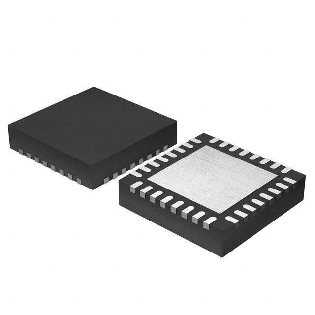
| 描述 | IC MCU 32BIT 128KB FLASH 64VFQFN |
| EEPROM容量 | - |
| 产品分类 | |
| I/O数 | 44 |
| 品牌 | Atmel |
| 数据手册 | |
| 产品图片 |
|
| 产品型号 | AT32UC3B0128-Z2UR |
| PCN其它 | |
| RAM容量 | 32K x 8 |
| rohs | 无铅 / 符合限制有害物质指令(RoHS)规范要求 |
| 产品系列 | AVR®32 UC3 B |
| 产品培训模块 | http://www.digikey.cn/PTM/IndividualPTM.page?site=cn&lang=zhs&ptm=24997http://www.digikey.cn/PTM/IndividualPTM.page?site=cn&lang=zhs&ptm=25676http://www.digikey.cn/PTM/IndividualPTM.page?site=cn&lang=zhs&ptm=26162http://www.digikey.cn/PTM/IndividualPTM.page?site=cn&lang=zhs&ptm=26159http://www.digikey.cn/PTM/IndividualPTM.page?site=cn&lang=zhs&ptm=26180 |
| 供应商器件封装 | * |
| 其它名称 | AT32UC3B0128-Z2URDKR |
| 包装 | Digi-Reel® |
| 外设 | 欠压检测/复位,DMA,POR,PWM,WDT |
| 封装/外壳 | 64-VFQFN 裸露焊盘 |
| 工作温度 | -40°C ~ 85°C |
| 振荡器类型 | 内部 |
| 数据转换器 | A/D 8x10b |
| 标准包装 | 1 |
| 核心处理器 | AVR |
| 核心尺寸 | 32-位 |
| 电压-电源(Vcc/Vdd) | 1.65 V ~ 3.6 V |
| 程序存储器类型 | 闪存 |
| 程序存储容量 | 128KB(128K x 8) |
| 连接性 | I²C, IrDA, SPI, SSC, UART/USART, USB |
| 速度 | 60MHz |


- 商务部:美国ITC正式对集成电路等产品启动337调查
- 曝三星4nm工艺存在良率问题 高通将骁龙8 Gen1或转产台积电
- 太阳诱电将投资9.5亿元在常州建新厂生产MLCC 预计2023年完工
- 英特尔发布欧洲新工厂建设计划 深化IDM 2.0 战略
- 台积电先进制程称霸业界 有大客户加持明年业绩稳了
- 达到5530亿美元!SIA预计今年全球半导体销售额将创下新高
- 英特尔拟将自动驾驶子公司Mobileye上市 估值或超500亿美元
- 三星加码芯片和SET,合并消费电子和移动部门,撤换高东真等 CEO
- 三星电子宣布重大人事变动 还合并消费电子和移动部门
- 海关总署:前11个月进口集成电路产品价值2.52万亿元 增长14.8%


PDF Datasheet 数据手册内容提取
Features • High Performance, Low Power 32-Bit Atmel® AVR®Microcontroller – Compact Single-cycle RISC Instruction Set Including DSP Instruction Set – Read-Modify-Write Instructions and Atomic Bit Manipulation – Performing up to 1.39 DMIPS / MHz • Up to 83 DMIPS Running at 60 MHz from Flash • Up to 46 DMIPS Running at 30 MHz from Flash – Memory Protection Unit • Multi-hierarchy Bus System 32-bit ATMEL – High-Performance Data Transfers on Separate Buses for Increased Performance – 7 Peripheral DMA Channels Improves Speed for Peripheral Communication AVR • Internal High-Speed Flash – 512K Bytes, 256K Bytes, 128K Bytes, 64K Bytes Versions Microcontroller – Single Cycle Access up to 30 MHz – Prefetch Buffer Optimizing Instruction Execution at Maximum Speed – 4ms Page Programming Time and 8ms Full-Chip Erase Time AT32UC3B0512 – 100,000 Write Cycles, 15-year Data Retention Capability – Flash Security Locks and User Defined Configuration Area AT32UC3B0256 • Internal High-Speed SRAM, Single-Cycle Access at Full Speed – 96K Bytes (512KB Flash), 32K Bytes (256KB and 128KB Flash), 16K Bytes (64KB AT32UC3B0128 Flash) • Interrupt Controller AT32UC3B064 – Autovectored Low Latency Interrupt Service with Programmable Priority • System Functions AT32UC3B1512 – Power and Clock Manager Including Internal RC Clock and One 32KHz Oscillator AT32UC3B1256 – Two Multipurpose Oscillators and Two Phase-Lock-Loop (PLL) allowing Independant CPU Frequency from USB Frequency AT32UC3B1128 – Watchdog Timer, Real-Time Clock Timer • Universal Serial Bus (USB) AT32UC3B164 – Device 2.0 and Embedded Host Low Speed and Full Speed – Flexible End-Point Configuration and Management with Dedicated DMA Channels – On-chip Transceivers Including Pull-Ups – USB Wake Up from Sleep Functionality • One Three-Channel 16-bit Timer/Counter (TC) – Three External Clock Inputs, PWM, Capture and Various Counting Capabilities • One 7-Channel 20-bit Pulse Width Modulation Controller (PWM) • Three Universal Synchronous/Asynchronous Receiver/Transmitters (USART) Summary – Independant Baudrate Generator, Support for SPI, IrDA and ISO7816 interfaces – Support for Hardware Handshaking, RS485 Interfaces and Modem Line • One Master/Slave Serial Peripheral Interfaces (SPI) with Chip Select Signals • One Synchronous Serial Protocol Controller – Supports I2S and Generic Frame-Based Protocols • One Master/Slave Two-Wire Interface (TWI), 400kbit/s I2C-compatible • One 8-channel 10-bit Analog-To-Digital Converter, 384ks/s • 16-bit Stereo Audio Bitstream DAC – Sample Rate Up to 50 KHz • QTouch® Library Support – Capacitive Touch Buttons, Sliders, and Wheels – QTouch and QMatrix Acquisition 32059L–01/2012
AT32UC3B • On-Chip Debug System (JTAG interface) – Nexus Class 2+, Runtime Control, Non-Intrusive Data and Program Trace • 64-pin TQFP/QFN (44 GPIO pins), 48-pin TQFP/QFN (28 GPIO pins) • 5V Input Tolerant I/Os, including 4 high-drive pins • Single 3.3V Power Supply or Dual 1.8V-3.3V Power Supply 2 32059L–AVR32–01/2012
AT32UC3B 1. Description The AT32UC3B is a complete System-On-Chip microcontroller based on the AVR32 UC RISC processor running at frequencies up to 60 MHz. AVR32 UC is a high-performance 32-bit RISC microprocessor core, designed for cost-sensitive embedded applications, with particular empha- sis on low power consumption, high code density and high performance. The processor implements a Memory Protection Unit (MPU) and a fast and flexible interrupt con- troller for supporting modern operating systems and real-time operating systems. Higher computation capability is achieved using a rich set of DSP instructions. The AT32UC3B incorporates on-chip Flash and SRAM memories for secure and fast access. The Peripheral Direct Memory Access controller enables data transfers between peripherals and memories without processor involvement. PDCA drastically reduces processing overhead when transferring continuous and large data streams between modules within the MCU. The Power Manager improves design flexibility and security: the on-chip Brown-Out Detector monitors the power supply, the CPU runs from the on-chip RC oscillator or from one of external oscillator sources, a Real-Time Clock and its associated timer keeps track of the time. The Timer/Counter includes three identical 16-bit timer/counter channels. Each channel can be independently programmed to perform frequency measurement, event counting, interval mea- surement, pulse generation, delay timing and pulse width modulation. The PWM modules provides seven independent channels with many configuration options including polarity, edge alignment and waveform non overlap control. One PWM channel can trigger ADC conversions for more accurate close loop control implementations. The AT32UC3B also features many communication interfaces for communication intensive applications. In addition to standard serial interfaces like USART, SPI or TWI, other interfaces like flexible Synchronous Serial Controller and USB are available. The USART supports different communication modes, like SPI mode. The Synchronous Serial Controller provides easy access to serial communication protocols and audio standards like I2S, UART or SPI. The Full-Speed USB 2.0 Device interface supports several USB Classes at the same time thanks to the rich End-Point configuration. The Embedded Host interface allows device like a USB Flash disk or a USB printer to be directly connected to the processor. Atmel offers the QTouch library for embedding capacitive touch buttons, sliders, and wheels functionality into AVR microcontrollers. The patented charge-transfer signal acquisition offers robust sensing and included fully debounced reporting of touch keys and includes Adjacent Key Suppression® (AKS®) technology for unambiguous detection of key events. The easy-to-use QTouch Suite toolchain allows you to explore, develop, and debug your own touch applications. AT32UC3B integrates a class 2+ Nexus 2.0 On-Chip Debug (OCD) System, with non-intrusive real-time trace, full-speed read/write memory access in addition to basic runtime control. The Nanotrace interface enables trace feature for JTAG-based debuggers. 3 32059L–AVR32–01/2012
AT32UC3B 2. Overview 2.1 Blockdiagram Figure 2-1. Block diagram TCK TTDDOI INTJETRAFGACE AVR32 UC ACE ILNOTCEARLF BAUCSE FAST GPIO TMS NEXUS CPU RF E MCKO CLASS 2+ NT MDO[5..0] OCD MEMORY PROTECTION UNIT Y I 16/32/96 KB MSEO[1..0] OR SRAM EVTI_N INSTR DATA EM EVTO_N INTERFACE INTERFACE M M M M S VBUS R D+ USB E DID- INTERFACE HIGH SPEED SHOLL 64/128/ VBOF DMA S BUS MATRIX S FLANTR 25F6L/5A1S2H KB M O C S S M CONFIGURATION REGISTERS BUS PB HSB HSB PERIPHERAL HSB-PB HSB-PB DMA BRIDGE B BRIDGE A CONTROLLER PB s O E I INTERRUPT OS CONTROLLER Os PPAB RAL PURP EXKTPISN[T7[.7.0..]0] IENXTTEERRRNUAPLT PDC USART1 DSR,R DTTRTCSRXX,L ,DCKD DTCSD, RI URPOSE I PPAB GENE NMI CONTROLLER C USART0 RTXXDD RAL P REAL TIME PD USART2 CLK NE COUNTER RTS, CTS GE SERIAL SCK DC PERIPHERAL MISO, MOSI WATCHDOG P INTERFACE NPCS[3..0] TIMER SYNCHRONOUS TX_CLOCK, TX_FRAME_SYNC 115 kHz POWER DC SERIAL TX_DATA RCOSC MANAGER P CONTROLLER RX_CLOCK, RX_FRAME_SYNC RX_DATA XIN32 32 KHz XOUT32 OSC CLOCK GENERATOR C TWO-WIRE SCL XIN0 OSC0 PD INTERFACE SDA XOUT0 CLOCK XXOIUNT11 OPSLLC01 CCOONNSTTLRREOOELLPLLEERR PDC CAONDNAIGVLOEITRGAT LTEOR AADDV[R7E..0F] PLL1 RESET AUDIO GCLK[3..0] CONTROLLER DC BITSTREAM DATA[1..0] RESET_N P DAC DATAN[1..0] A[2..0] B[2..0] TIMER/COUNTER PULSE WIDTH CLK[2..0] MODULATION PWM[6..0] CONTROLLER 4 32059L–AVR32–01/2012
AT32UC3B 3. Configuration Summary The table below lists all AT32UC3B memory and package configurations: Table 3-1. Configuration Summary Feature AT32UC3B0512 AT32UC3B0256/128/64 AT32UC3B1512 AT32UC3B1256/128/64 Flash 512 KB 256/128/64 KB 512 KB 256/128/64 KB SRAM 96KB 32/32/16KB 96KB 32/16/16KB GPIO 44 28 External Interrupts 8 6 TWI 1 USART 3 Peripheral DMA Channels 7 SPI 1 Full Speed USB Mini-Host + Device Device SSC 1 0 Audio Bitstream DAC 1 0 1 0 Timer/Counter Channels 3 PWM Channels 7 Watchdog Timer 1 Real-Time Clock Timer 1 Power Manager 1 PLL 80-240 MHz (PLL0/PLL1) Crystal Oscillators 0.4-20 MHz (OSC0) Crystal Oscillator 32 KHz (OSC32K) Oscillators RC Oscillator 115 kHz (RCSYS) Crystal Oscillators 0.4-20 MHz (OSC1) 10-bit ADC 8 6 number of channels JTAG 1 Max Frequency 60 MHz Package TQFP64, QFN64 TQFP48, QFN48 5 32059L–AVR32–01/2012
AT32UC3B 4. Package and Pinout 4.1 Package The device pins are multiplexed with peripheral functions as described in the Peripheral Multi- plexing on I/O Line section. Figure 4-1. TQFP64 / QFN64 Pinout O DI232221200729281918061716151413 DAAAABAAAABAAAAA VPPPPPPPPPPPPPPP 8765432109876543 4444444443333333 GND 49 32 VDDIO DP 50 31 PA12 DM 51 30 PA11 VBUS 52 29 PA10 VDDPLL 53 28 PA09 PB08 54 27 PB05 PB09 55 26 PB04 VDDCORE 56 25 PB03 PB10 57 24 PB02 PB11 58 23 GND PA24 59 22 VDDCORE PA25 60 21 VDDIN PA26 61 20 VDDOUT PA27 62 19 VDDANA RESET_N 63 18 ADVREF VDDIO 64 17 GNDANA 1111111 1234567890123456 GTPPPPPVPPPPPPPP NCAAABBDAAAAAAAA DK00000D00000033 01201C34567801 O R E 6 32059L–AVR32–01/2012
AT32UC3B Figure 4-2. TQFP48 / QFN48 Pinout O DI2322212019181716151413 DAAAAAAAAAAA VPPPPPPPPPPP 654321098765 333333322222 GND 37 24 VDDIO DP 38 23 PA12 DM 39 22 PA11 VBUS 40 21 PA10 VDDPLL 41 20 PA09 VDDCORE 42 19 GND PA24 43 18 VDDCORE PA25 44 17 VDDIN PA26 45 16 VDDOUT PA27 46 15 VDDANA RESET_N 47 14 ADVREF VDDIO 48 13 GNDANA 111 123456789012 GTPPPVPPPPPP NCAAADAAAAAA DK000D000000 012C345678 O R E Note: The exposed pad is not connected to anything internally, but should be soldered to ground to increase board level reliability. 4.2 Peripheral Multiplexing on I/O lines 4.2.1 Multiplexed signals Each GPIO line can be assigned to one of 4 peripheral functions; A, B, C or D (D is only avail- able for UC3Bx512 parts). The following table define how the I/O lines on the peripherals A, B,C or D are multiplexed by the GPIO. Table 4-1. GPIO Controller Function Multiplexing Function D 48-pin 64-pin PIN GPIO Pin Function A Function B Function C (only for UC3Bx512) 3 3 PA00 GPIO 0 4 4 PA01 GPIO 1 5 5 PA02 GPIO 2 7 9 PA03 GPIO 3 ADC - AD[0] PM - GCLK[0] USBB - USB_ID ABDAC - DATA[0] 8 10 PA04 GPIO 4 ADC - AD[1] PM - GCLK[1] USBB - USB_VBOF ABDAC - DATAN[0] 9 11 PA05 GPIO 5 EIC - EXTINT[0] ADC - AD[2] USART1 - DCD ABDAC - DATA[1] 7 32059L–AVR32–01/2012
AT32UC3B Table 4-1. GPIO Controller Function Multiplexing 10 12 PA06 GPIO 6 EIC - EXTINT[1] ADC - AD[3] USART1 - DSR ABDAC - DATAN[1] SSC - 11 13 PA07 GPIO 7 PWM - PWM[0] ADC - AD[4] USART1 - DTR RX_FRAME_SYNC 12 14 PA08 GPIO 8 PWM - PWM[1] ADC - AD[5] USART1 - RI SSC - RX_CLOCK 20 28 PA09 GPIO 9 TWI - SCL SPI0 - NPCS[2] USART1 - CTS 21 29 PA10 GPIO 10 TWI - SDA SPI0 - NPCS[3] USART1 - RTS 22 30 PA11 GPIO 11 USART0 - RTS TC - A2 PWM - PWM[0] SSC - RX_DATA 23 31 PA12 GPIO 12 USART0 - CTS TC - B2 PWM - PWM[1] USART1 - TXD 25 33 PA13 GPIO 13 EIC - NMI PWM - PWM[2] USART0 - CLK SSC - RX_CLOCK 26 34 PA14 GPIO 14 SPI0 - MOSI PWM - PWM[3] EIC - EXTINT[2] PM - GCLK[2] 27 35 PA15 GPIO 15 SPI0 - SCK PWM - PWM[4] USART2 - CLK 28 36 PA16 GPIO 16 SPI0 - NPCS[0] TC - CLK1 PWM - PWM[4] 29 37 PA17 GPIO 17 SPI0 - NPCS[1] TC - CLK2 SPI0 - SCK USART1 - RXD SSC - 30 39 PA18 GPIO 18 USART0 - RXD PWM - PWM[5] SPI0 - MISO RX_FRAME_SYNC 31 40 PA19 GPIO 19 USART0 - TXD PWM - PWM[6] SPI0 - MOSI SSC - TX_CLOCK 32 44 PA20 GPIO 20 USART1 - CLK TC - CLK0 USART2 - RXD SSC - TX_DATA SSC - 33 45 PA21 GPIO 21 PWM - PWM[2] TC - A1 USART2 - TXD TX_FRAME_SYNC 34 46 PA22 GPIO 22 PWM - PWM[6] TC - B1 ADC - TRIGGER ABDAC - DATA[0] 35 47 PA23 GPIO 23 USART1 - TXD SPI0 - NPCS[1] EIC - EXTINT[3] PWM - PWM[0] 43 59 PA24 GPIO 24 USART1 - RXD SPI0 - NPCS[0] EIC - EXTINT[4] PWM - PWM[1] 44 60 PA25 GPIO 25 SPI0 - MISO PWM - PWM[3] EIC - EXTINT[5] 45 61 PA26 GPIO 26 USBB - USB_ID USART2 - TXD TC - A0 ABDAC - DATA[1] 46 62 PA27 GPIO 27 USBB - USB_VBOF USART2 - RXD TC - B0 ABDAC - DATAN[1] 41 PA28 GPIO 28 USART0 - CLK PWM - PWM[4] SPI0 - MISO ABDAC - DATAN[0] 42 PA29 GPIO 29 TC - CLK0 TC - CLK1 SPI0 - MOSI 15 PA30 GPIO 30 ADC - AD[6] EIC - SCAN[0] PM - GCLK[2] 16 PA31 GPIO 31 ADC - AD[7] EIC - SCAN[1] PWM - PWM[6] 6 PB00 GPIO 32 TC - A0 EIC - SCAN[2] USART2 - CTS 7 PB01 GPIO 33 TC - B0 EIC - SCAN[3] USART2 - RTS 24 PB02 GPIO 34 EIC - EXTINT[6] TC - A1 USART1 - TXD 25 PB03 GPIO 35 EIC - EXTINT[7] TC - B1 USART1 - RXD 26 PB04 GPIO 36 USART1 - CTS SPI0 - NPCS[3] TC - CLK2 27 PB05 GPIO 37 USART1 - RTS SPI0 - NPCS[2] PWM - PWM[5] 38 PB06 GPIO 38 SSC - RX_CLOCK USART1 - DCD EIC - SCAN[4] ABDAC - DATA[0] 43 PB07 GPIO 39 SSC - RX_DATA USART1 - DSR EIC - SCAN[5] ABDAC - DATAN[0] SSC - 54 PB08 GPIO 40 USART1 - DTR EIC - SCAN[6] ABDAC - DATA[1] RX_FRAME_SYNC 8 32059L–AVR32–01/2012
AT32UC3B Table 4-1. GPIO Controller Function Multiplexing 55 PB09 GPIO 41 SSC - TX_CLOCK USART1 - RI EIC - SCAN[7] ABDAC - DATAN[1] 57 PB10 GPIO 42 SSC - TX_DATA TC - A2 USART0 - RXD SSC - 58 PB11 GPIO 43 TC - B2 USART0 - TXD TX_FRAME_SYNC 4.2.2 JTAG Port Connections If the JTAG is enabled, the JTAG will take control over a number of pins, irrespective of the I/O Controller configuration. Table 4-2. JTAG Pinout 64QFP/QFN 48QFP/QFN Pin name JTAG pin 2 2 TCK TCK 3 3 PA00 TDI 4 4 PA01 TDO 5 5 PA02 TMS 4.2.3 Nexus OCD AUX port connections If the OCD trace system is enabled, the trace system will take control over a number of pins, irre- spectively of the PIO configuration. Two different OCD trace pin mappings are possible, depending on the configuration of the OCD AXS register. For details, see the AVR32 UC Tech- nical Reference Manual. Table 4-3. Nexus OCD AUX port connections Pin AXS=0 AXS=1 EVTI_N PB05 PA14 MDO[5] PB04 PA08 MDO[4] PB03 PA07 MDO[3] PB02 PA06 MDO[2] PB01 PA05 MDO[1] PB00 PA04 MDO[0] PA31 PA03 EVTO_N PA15 PA15 MCKO PA30 PA13 MSEO[1] PB06 PA09 MSEO[0] PB07 PA10 4.2.4 Oscillator Pinout The oscillators are not mapped to the normal A, B or C functions and their muxings are con- trolled by registers in the Power Manager (PM). Please refer to the power manager chapter for more information about this. 9 32059L–AVR32–01/2012
AT32UC3B Table 4-4. Oscillator pinout QFP48 pin QFP64 pin Pad Oscillator pin 30 39 PA18 XIN0 41 PA28 XIN1 22 30 PA11 XIN32 31 40 PA19 XOUT0 42 PA29 XOUT1 23 31 PA12 XOUT32 4.3 High Drive Current GPIO Ones of GPIOs can be used to drive twice current than other GPIO capability (see Electrical Characteristics section). Table 4-5. High Drive Current GPIO GPIO Name PA20 PA21 PA22 PA23 5. Signals Description The following table gives details on the signal name classified by peripheral. Table 5-1. Signal Description List Active Signal Name Function Type Level Comments Power Power VDDPLL PLL Power Supply 1.65V to 1.95 V Input Power VDDCORE Core Power Supply 1.65V to 1.95 V Input Power VDDIO I/O Power Supply 3.0V to 3.6V Input Power VDDANA Analog Power Supply 3.0V to 3.6V Input Power VDDIN Voltage Regulator Input Supply 3.0V to 3.6V Input 10 32059L–AVR32–01/2012
AT32UC3B Table 5-1. Signal Description List (Continued) Active Signal Name Function Type Level Comments Power VDDOUT Voltage Regulator Output 1.65V to 1.95 V Output GNDANA Analog Ground Ground GND Ground Ground Clocks, Oscillators, and PLL’s XIN0, XIN1, XIN32 Crystal 0, 1, 32 Input Analog XOUT0, XOUT1, Crystal 0, 1, 32 Output Analog XOUT32 JTAG TCK Test Clock Input TDI Test Data In Input TDO Test Data Out Output TMS Test Mode Select Input Auxiliary Port - AUX MCKO Trace Data Output Clock Output MDO0 - MDO5 Trace Data Output Output MSEO0 - MSEO1 Trace Frame Control Output EVTI_N Event In Output Low EVTO_N Event Out Output Low Power Manager - PM GCLK0 - GCLK2 Generic Clock Pins Output RESET_N Reset Pin Input Low External Interrupt Controller - EIC EXTINT0 - EXTINT7 External Interrupt Pins Input KPS0 - KPS7 Keypad Scan Pins Output NMI Non-Maskable Interrupt Pin Input Low General Purpose I/O pin- GPIOA, GPIOB PA0 - PA31 Parallel I/O Controller GPIOA I/O PB0 - PB11 Parallel I/O Controller GPIOB I/O 11 32059L–AVR32–01/2012
AT32UC3B Table 5-1. Signal Description List (Continued) Active Signal Name Function Type Level Comments Serial Peripheral Interface - SPI0 MISO Master In Slave Out I/O MOSI Master Out Slave In I/O NPCS0 - NPCS3 SPI Peripheral Chip Select I/O Low SCK Clock Output Synchronous Serial Controller - SSC RX_CLOCK SSC Receive Clock I/O RX_DATA SSC Receive Data Input RX_FRAME_SYNC SSC Receive Frame Sync I/O TX_CLOCK SSC Transmit Clock I/O TX_DATA SSC Transmit Data Output TX_FRAME_SYNC SSC Transmit Frame Sync I/O Timer/Counter - TIMER A0 Channel 0 Line A I/O A1 Channel 1 Line A I/O A2 Channel 2 Line A I/O B0 Channel 0 Line B I/O B1 Channel 1 Line B I/O B2 Channel 2 Line B I/O CLK0 Channel 0 External Clock Input Input CLK1 Channel 1 External Clock Input Input CLK2 Channel 2 External Clock Input Input Two-wire Interface - TWI SCL Serial Clock I/O SDA Serial Data I/O Universal Synchronous Asynchronous Receiver Transmitter - USART0, USART1, USART2 CLK Clock I/O CTS Clear To Send Input 12 32059L–AVR32–01/2012
AT32UC3B Table 5-1. Signal Description List (Continued) Active Signal Name Function Type Level Comments DCD Data Carrier Detect Only USART1 DSR Data Set Ready Only USART1 DTR Data Terminal Ready Only USART1 RI Ring Indicator Only USART1 RTS Request To Send Output RXD Receive Data Input TXD Transmit Data Output Analog to Digital Converter - ADC Analog AD0 - AD7 Analog input pins input Analog ADVREF Analog positive reference voltage input 2.6 to 3.6V input Audio Bitstream DAC - ABDAC DATA0 - DATA1 D/A Data out Output DATAN0 - DATAN1 D/A Data inverted out Output Pulse Width Modulator - PWM PWM0 - PWM6 PWM Output Pins Output Universal Serial Bus Device - USBB DDM USB Device Port Data - Analog DDP USB Device Port Data + Analog USB VBUS Monitor and Embedded Host Analog VBUS Negociation Input USBID ID Pin of the USB Bus Input USB_VBOF USB VBUS On/off: bus power control port output 5.1 JTAG pins TMS and TDI pins have pull-up resistors. TDO pin is an output, driven at up to VDDIO, and has no pull-up resistor. These 3 pins can be used as GPIO-pins. At reset state, these pins are in GPIO mode. TCK pin cannot be used as GPIO pin. JTAG interface is enabled when TCK pin is tied low. 13 32059L–AVR32–01/2012
AT32UC3B 5.2 RESET_N pin The RESET_N pin is a schmitt input and integrates a permanent pull-up resistor to VDDIO. As the product integrates a power-on reset cell, the RESET_N pin can be left unconnected in case no reset from the system needs to be applied to the product. 5.3 TWI pins When these pins are used for TWI, the pins are open-drain outputs with slew-rate limitation and inputs with inputs with spike-filtering. When used as GPIO-pins or used for other peripherals, the pins have the same characteristics as GPIO pins. 5.4 GPIO pins All the I/O lines integrate a pull-up resistor. Programming of this pull-up resistor is performed independently for each I/O line through the GPIO Controllers. After reset, I/O lines default as inputs with pull-up resistors disabled, except when indicated otherwise in the column “Reset Value” of the GPIO Controller user interface table. 5.5 High drive pins The four pins PA20, PA21, PA22, PA23 have high drive output capabilities. 5.6 Power Considerations 5.6.1 Power Supplies The AT32UC3B has several types of power supply pins: • VDDIO: Powers I/O lines. Voltage is 3.3V nominal. • VDDANA: Powers the ADC Voltage is 3.3V nominal. • VDDIN: Input voltage for the voltage regulator. Voltage is 3.3V nominal. • VDDCORE: Powers the core, memories, and peripherals. Voltage is 1.8V nominal. • VDDPLL: Powers the PLL. Voltage is 1.8V nominal. The ground pins GND are common to VDDCORE, VDDIO and VDDPLL. The ground pin for VDDANA is GNDANA. Refer to Electrical Characteristics section for power consumption on the various supply pins. The main requirement for power supplies connection is to respect a star topology for all electrical connection. 14 32059L–AVR32–01/2012
AT32UC3B Figure 5-1. Power Supply Dual Power Supply Single Power Supply 3.3V VDDANA 3.3V VDDANA VDDIO VDDIO ADVREF ADVREF VDDIN VDDIN 1.8V 1.8V Regulator Regulator VDDOUT VDDOUT 1.8 VDDCORE V VDDCORE VDDPLL VDDPLL 5.6.2 Voltage Regulator 5.6.2.1 Single Power Supply The AT32UC3B embeds a voltage regulator that converts from 3.3V to 1.8V. The regulator takes its input voltage from VDDIN, and supplies the output voltage on VDDOUT that should be exter- nally connected to the 1.8V domains. Adequate input supply decoupling is mandatory for VDDIN in order to improve startup stability and reduce source voltage drop. Two input decoupling capacitors must be placed close to the chip. Adequate output supply decoupling is mandatory for VDDOUT to reduce ripple and avoid oscil- lations. The best way to achieve this is to use two capacitors in parallel between VDDOUT and GND as close to the chip as possible Figure 5-2. Supply Decoupling 3.3V VDDIN CIN2 CIN1 1.8V Regulator 1.8V VDDOUT C C OUT2 OUT1 15 32059L–AVR32–01/2012
AT32UC3B Refer to Section 9.3 on page 38 for decoupling capacitors values and regulator characteristics. For decoupling recommendations for VDDIO, VDDANA, VDDCORE and VDDPLL, please refer to the Schematic checklist. 5.6.2.2 Dual Power Supply In case of dual power supply, VDDIN and VDDOUT should be connected to ground to prevent from leakage current. To avoid over consumption during the power up sequence, VDDIO and VDDCORE voltage dif- ference needs to stay in the range given Figure 5-3. Figure 5-3. VDDIO versus VDDCORE during power up sequence 4 Extra consumption on VDDIO 3.5 3 2.5 V) O ( 2 DI D V 1.5 1 0.5 Extra consumption on VDDCORE 0 0 0.2 0.4 0.6 0.8 1 1.2 1.4 1.6 1.8 2 VDDCORE (V) 5.6.3 Analog-to-Digital Converter (ADC) reference. The ADC reference (ADVREF) must be provided from an external source. Two decoupling capacitors must be used to insure proper decoupling. Figure 5-4. ADVREF Decoupling 3.3V ADVREF C C VREF2 VREF1 Refer to Section 9.4 on page 38 for decoupling capacitors values and electrical characteristics. In case ADC is not used, the ADVREF pin should be connected to GND to avoid extra consumption. 16 32059L–AVR32–01/2012
AT32UC3B 6. Processor and Architecture Rev: 1.0.0.0 This chapter gives an overview of the AVR32UC CPU. AVR32UC is an implementation of the AVR32 architecture. A summary of the programming model, instruction set, and MPU is pre- sented. For further details, see the AVR32 Architecture Manual and the AVR32UC Technical Reference Manual. 6.1 Features • 32-bit load/store AVR32A RISC architecture – 15 general-purpose 32-bit registers – 32-bit Stack Pointer, Program Counter and Link Register reside in register file – Fully orthogonal instruction set – Privileged and unprivileged modes enabling efficient and secure Operating Systems – Innovative instruction set together with variable instruction length ensuring industry leading code density – DSP extention with saturating arithmetic, and a wide variety of multiply instructions • 3-stage pipeline allows one instruction per clock cycle for most instructions – Byte, halfword, word and double word memory access – Multiple interrupt priority levels • MPU allows for operating systems with memory protection 6.2 AVR32 Architecture AVR32 is a high-performance 32-bit RISC microprocessor architecture, designed for cost-sensi- tive embedded applications, with particular emphasis on low power consumption and high code density. In addition, the instruction set architecture has been tuned to allow a variety of micro- architectures, enabling the AVR32 to be implemented as low-, mid-, or high-performance processors. AVR32 extends the AVR family into the world of 32- and 64-bit applications. Through a quantitative approach, a large set of industry recognized benchmarks has been com- piled and analyzed to achieve the best code density in its class. In addition to lowering the memory requirements, a compact code size also contributes to the core’s low power characteris- tics. The processor supports byte and halfword data types without penalty in code size and performance. Memory load and store operations are provided for byte, halfword, word, and double word data with automatic sign- or zero extension of halfword and byte data. The C-compiler is closely linked to the architecture and is able to exploit code optimization features, both for size and speed. In order to reduce code size to a minimum, some instructions have multiple addressing modes. As an example, instructions with immediates often have a compact format with a smaller imme- diate, and an extended format with a larger immediate. In this way, the compiler is able to use the format giving the smallest code size. Another feature of the instruction set is that frequently used instructions, like add, have a com- pact format with two operands as well as an extended format with three operands. The larger format increases performance, allowing an addition and a data move in the same instruction in a single cycle. Load and store instructions have several different formats in order to reduce code size and speed up execution. 17 32059L–AVR32–01/2012
AT32UC3B The register file is organized as sixteen 32-bit registers and includes the Program Counter, the Link Register, and the Stack Pointer. In addition, register R12 is designed to hold return values from function calls and is used implicitly by some instructions. 6.3 The AVR32UC CPU The AVR32UC CPU targets low- and medium-performance applications, and provides an advanced OCD system, no caches, and a Memory Protection Unit (MPU). Java acceleration hardware is not implemented. AVR32UC provides three memory interfaces, one High Speed Bus master for instruction fetch, one High Speed Bus master for data access, and one High Speed Bus slave interface allowing other bus masters to access data RAMs internal to the CPU. Keeping data RAMs internal to the CPU allows fast access to the RAMs, reduces latency, and guarantees deterministic timing. Also, power consumption is reduced by not needing a full High Speed Bus access for memory accesses. A dedicated data RAM interface is provided for communicating with the internal data RAMs. A local bus interface is provided for connecting the CPU to device-specific high-speed systems, such as floating-point units and fast GPIO ports. This local bus has to be enabled by writing the LOCEN bit in the CPUCR system register. The local bus is able to transfer data between the CPU and the local bus slave in a single clock cycle. The local bus has a dedicated memory range allocated to it, and data transfers are performed using regular load and store instructions. Details on which devices that are mapped into the local bus space is given in the Memories chapter of this data sheet. Figure 6-1 on page 19 displays the contents of AVR32UC. 18 32059L–AVR32–01/2012
AT32UC3B Figure 6-1. Overview of the AVR32UC CPU er interface OCD interface Reset interface oll ntr Power/ o OCD upt c system Reset err control nt I AVR32UC CPU pipeline MPU Instruction memory controller Data memory controller High High CPU Local Speed High Speed Bus master Speed Bus Bus Bus slave master e master ac erf gh Speed Bus gh Speed Bus gh Speed Bus PU Local Bus Data RAM int Hi Hi Hi C 6.3.1 Pipeline Overview AVR32UC has three pipeline stages, Instruction Fetch (IF), Instruction Decode (ID), and Instruc- tion Execute (EX). The EX stage is split into three parallel subsections, one arithmetic/logic (ALU) section, one multiply (MUL) section, and one load/store (LS) section. Instructions are issued and complete in order. Certain operations require several clock cycles to complete, and in this case, the instruction resides in the ID and EX stages for the required num- ber of clock cycles. Since there is only three pipeline stages, no internal data forwarding is required, and no data dependencies can arise in the pipeline. Figure 6-2 on page 20 shows an overview of the AVR32UC pipeline stages. 19 32059L–AVR32–01/2012
AT32UC3B Figure 6-2. The AVR32UC Pipeline MUL Multiply unit Regfile Regfile IF ID ALU ALU unit Read write Prefetch unit Decode unit Load-store LS unit 6.3.2 AVR32A Microarchitecture Compliance AVR32UC implements an AVR32A microarchitecture. The AVR32A microarchitecture is tar- geted at cost-sensitive, lower-end applications like smaller microcontrollers. This microarchitecture does not provide dedicated hardware registers for shadowing of register file registers in interrupt contexts. Additionally, it does not provide hardware registers for the return address registers and return status registers. Instead, all this information is stored on the system stack. This saves chip area at the expense of slower interrupt handling. Upon interrupt initiation, registers R8-R12 are automatically pushed to the system stack. These registers are pushed regardless of the priority level of the pending interrupt. The return address and status register are also automatically pushed to stack. The interrupt handler can therefore use R8-R12 freely. Upon interrupt completion, the old R8-R12 registers and status register are restored, and execution continues at the return address stored popped from stack. The stack is also used to store the status register and return address for exceptions and scall. Executing the rete or rets instruction at the completion of an exception or system call will pop this status register and continue execution at the popped return address. 6.3.3 Java Support AVR32UC does not provide Java hardware acceleration. 6.3.4 Memory Protection The MPU allows the user to check all memory accesses for privilege violations. If an access is attempted to an illegal memory address, the access is aborted and an exception is taken. The MPU in AVR32UC is specified in the AVR32UC Technical Reference manual. 6.3.5 Unaligned Reference Handling AVR32UC does not support unaligned accesses, except for doubleword accesses. AVR32UC is able to perform word-aligned st.d and ld.d. Any other unaligned memory access will cause an address exception. Doubleword-sized accesses with word-aligned pointers will automatically be performed as two word-sized accesses. 20 32059L–AVR32–01/2012
AT32UC3B The following table shows the instructions with support for unaligned addresses. All other instructions require aligned addresses. Table 6-1. Instructions with Unaligned Reference Support Instruction Supported alignment ld.d Word st.d Word 6.3.6 Unimplemented Instructions The following instructions are unimplemented in AVR32UC, and will cause an Unimplemented Instruction Exception if executed: • All SIMD instructions • All coprocessor instructions if no coprocessors are present • retj, incjosp, popjc, pushjc • tlbr, tlbs, tlbw • cache 6.3.7 CPU and Architecture Revision Three major revisions of the AVR32UC CPU currently exist. The Architecture Revision field in the CONFIG0 system register identifies which architecture revision is implemented in a specific device. AVR32UC CPU revision 3 is fully backward-compatible with revisions 1 and 2, ie. code compiled for revision 1 or 2 is binary-compatible with revision 3 CPUs. 21 32059L–AVR32–01/2012
AT32UC3B 6.4 Programming Model 6.4.1 Register File Configuration The AVR32UC register file is shown below. Figure 6-3. The AVR32UC Register File Application Supervisor INT0 INT1 INT2 INT3 Exception NMI Secure Bit 31 Bit 0 Bit 31 Bit 0 Bit 31 Bit 0 Bit 31 Bit 0 Bit 31 Bit 0 Bit 31 Bit 0 Bit 31 Bit 0 Bit 31 Bit 0 Bit 31 Bit 0 PC PC PC PC PC PC PC PC PC LR LR LR LR LR LR LR LR LR SP_APP SP_SYS SP_SYS SP_SYS SP_SYS SP_SYS SP_SYS SP_SYS SP_SEC R12 R12 R12 R12 R12 R12 R12 R12 R12 R11 R11 R11 R11 R11 R11 R11 R11 R11 R10 R10 R10 R10 R10 R10 R10 R10 R10 R9 R9 R9 R9 R9 R9 R9 R9 R9 R8 R8 R8 R8 R8 R8 R8 R8 R8 INTR07PC INTR07PC INTR07PC INTR07PC INTR07PC INTR07PC INTR07PC INTR07PC INTR07PC INTR16PC INTR16PC INTR16PC INTR16PC INTR16PC INTR16PC INTR16PC INTR16PC INTR16PC FINRT5PC FINRT5PC FINRT5PC FINRT5PC FINRT5PC FINRT5PC FINRT5PC FINRT5PC FINRT5PC SMRP4C SMRP4C SMRP4C SMRP4C SMRP4C SMRP4C SMRP4C SMRP4C SMRP4C R3 R3 R3 R3 R3 R3 R3 R3 R3 R2 R2 R2 R2 R2 R2 R2 R2 R2 R1 R1 R1 R1 R1 R1 R1 R1 R1 R0 R0 R0 R0 R0 R0 R0 R0 R0 SR SR SR SR SR SR SR SR SR SS_STATUS SS_ADRF SS_ADRR SS_ADR0 SS_ADR1 SS_SP_SYS SS_SP_APP SS_RAR SS_RSR 6.4.2 Status Register Configuration The Status Register (SR) is split into two halfwords, one upper and one lower, see Figure 6-4 on page 22 and Figure 6-5 on page 23. The lower word contains the C, Z, N, V, and Q condition code flags and the R, T, and L bits, while the upper halfword contains information about the mode and state the processor executes in. Refer to the AVR32 Architecture Manual for details. Figure 6-4. The Status Register High Halfword Bit 31 Bit 16 LC - - - - DM D - M2 M1 M0 EM I3M IF2EM I1M I0M GM Bit name 1 0 0 0 0 0 0 0 0 0 1 1 0 0 0 0 1 Initial value Global Interrupt Mask Interrupt Level 0 Mask Interrupt Level 1 Mask Interrupt Level 2 Mask Interrupt Level 3 Mask Exception Mask Mode Bit 0 Mode Bit 1 Mode Bit 2 Reserved Debug State Debug State Mask Reserved 22 32059L–AVR32–01/2012
AT32UC3B Figure 6-5. The Status Register Low Halfword Bit 15 Bit 0 - T - - - - - - - - L Q V N Z C Bit name 0 0 0 0 0 0 0 0 0 0 0 0 0 0 0 0 Initial value Carry Zero Sign Overflow Saturation Lock Reserved Scratch Reserved 6.4.3 Processor States 6.4.3.1 Normal RISC State The AVR32 processor supports several different execution contexts as shown in Table 6-2 on page 23. Table 6-2. Overview of Execution Modes, their Priorities and Privilege Levels. Priority Mode Security Description 1 Non Maskable Interrupt Privileged Non Maskable high priority interrupt mode 2 Exception Privileged Execute exceptions 3 Interrupt 3 Privileged General purpose interrupt mode 4 Interrupt 2 Privileged General purpose interrupt mode 5 Interrupt 1 Privileged General purpose interrupt mode 6 Interrupt 0 Privileged General purpose interrupt mode N/A Supervisor Privileged Runs supervisor calls N/A Application Unprivileged Normal program execution mode Mode changes can be made under software control, or can be caused by external interrupts or exception processing. A mode can be interrupted by a higher priority mode, but never by one with lower priority. Nested exceptions can be supported with a minimal software overhead. When running an operating system on the AVR32, user processes will typically execute in the application mode. The programs executed in this mode are restricted from executing certain instructions. Furthermore, most system registers together with the upper halfword of the status register cannot be accessed. Protected memory areas are also not available. All other operating modes are privileged and are collectively called System Modes. They have full access to all priv- ileged and unprivileged resources. After a reset, the processor will be in supervisor mode. 6.4.3.2 Debug State The AVR32 can be set in a debug state, which allows implementation of software monitor rou- tines that can read out and alter system information for use during application development. This implies that all system and application registers, including the status registers and program counters, are accessible in debug state. The privileged instructions are also available. 23 32059L–AVR32–01/2012
AT32UC3B All interrupt levels are by default disabled when debug state is entered, but they can individually be switched on by the monitor routine by clearing the respective mask bit in the status register. Debug state can be entered as described in the AVR32UC Technical Reference Manual. Debug state is exited by the retd instruction. 6.4.4 System Registers The system registers are placed outside of the virtual memory space, and are only accessible using the privileged mfsr and mtsr instructions. The table below lists the system registers speci- fied in the AVR32 architecture, some of which are unused in AVR32UC. The programmer is responsible for maintaining correct sequencing of any instructions following a mtsr instruction. For detail on the system registers, refer to the AVR32UC Technical Reference Manual. Table 6-3. System Registers Reg # Address Name Function 0 0 SR Status Register 1 4 EVBA Exception Vector Base Address 2 8 ACBA Application Call Base Address 3 12 CPUCR CPU Control Register 4 16 ECR Exception Cause Register 5 20 RSR_SUP Unused in AVR32UC 6 24 RSR_INT0 Unused in AVR32UC 7 28 RSR_INT1 Unused in AVR32UC 8 32 RSR_INT2 Unused in AVR32UC 9 36 RSR_INT3 Unused in AVR32UC 10 40 RSR_EX Unused in AVR32UC 11 44 RSR_NMI Unused in AVR32UC 12 48 RSR_DBG Return Status Register for Debug mode 13 52 RAR_SUP Unused in AVR32UC 14 56 RAR_INT0 Unused in AVR32UC 15 60 RAR_INT1 Unused in AVR32UC 16 64 RAR_INT2 Unused in AVR32UC 17 68 RAR_INT3 Unused in AVR32UC 18 72 RAR_EX Unused in AVR32UC 19 76 RAR_NMI Unused in AVR32UC 20 80 RAR_DBG Return Address Register for Debug mode 21 84 JECR Unused in AVR32UC 22 88 JOSP Unused in AVR32UC 23 92 JAVA_LV0 Unused in AVR32UC 24 96 JAVA_LV1 Unused in AVR32UC 25 100 JAVA_LV2 Unused in AVR32UC 24 32059L–AVR32–01/2012
AT32UC3B Table 6-3. System Registers (Continued) Reg # Address Name Function 26 104 JAVA_LV3 Unused in AVR32UC 27 108 JAVA_LV4 Unused in AVR32UC 28 112 JAVA_LV5 Unused in AVR32UC 29 116 JAVA_LV6 Unused in AVR32UC 30 120 JAVA_LV7 Unused in AVR32UC 31 124 JTBA Unused in AVR32UC 32 128 JBCR Unused in AVR32UC 33-63 132-252 Reserved Reserved for future use 64 256 CONFIG0 Configuration register 0 65 260 CONFIG1 Configuration register 1 66 264 COUNT Cycle Counter register 67 268 COMPARE Compare register 68 272 TLBEHI Unused in AVR32UC 69 276 TLBELO Unused in AVR32UC 70 280 PTBR Unused in AVR32UC 71 284 TLBEAR Unused in AVR32UC 72 288 MMUCR Unused in AVR32UC 73 292 TLBARLO Unused in AVR32UC 74 296 TLBARHI Unused in AVR32UC 75 300 PCCNT Unused in AVR32UC 76 304 PCNT0 Unused in AVR32UC 77 308 PCNT1 Unused in AVR32UC 78 312 PCCR Unused in AVR32UC 79 316 BEAR Bus Error Address Register 80 320 MPUAR0 MPU Address Register region 0 81 324 MPUAR1 MPU Address Register region 1 82 328 MPUAR2 MPU Address Register region 2 83 332 MPUAR3 MPU Address Register region 3 84 336 MPUAR4 MPU Address Register region 4 85 340 MPUAR5 MPU Address Register region 5 86 344 MPUAR6 MPU Address Register region 6 87 348 MPUAR7 MPU Address Register region 7 88 352 MPUPSR0 MPU Privilege Select Register region 0 89 356 MPUPSR1 MPU Privilege Select Register region 1 90 360 MPUPSR2 MPU Privilege Select Register region 2 91 364 MPUPSR3 MPU Privilege Select Register region 3 25 32059L–AVR32–01/2012
AT32UC3B Table 6-3. System Registers (Continued) Reg # Address Name Function 92 368 MPUPSR4 MPU Privilege Select Register region 4 93 372 MPUPSR5 MPU Privilege Select Register region 5 94 376 MPUPSR6 MPU Privilege Select Register region 6 95 380 MPUPSR7 MPU Privilege Select Register region 7 96 384 MPUCRA Unused in this version of AVR32UC 97 388 MPUCRB Unused in this version of AVR32UC 98 392 MPUBRA Unused in this version of AVR32UC 99 396 MPUBRB Unused in this version of AVR32UC 100 400 MPUAPRA MPU Access Permission Register A 101 404 MPUAPRB MPU Access Permission Register B 102 408 MPUCR MPU Control Register 103-191 448-764 Reserved Reserved for future use 192-255 768-1020 IMPL IMPLEMENTATION DEFINED 6.5 Exceptions and Interrupts AVR32UC incorporates a powerful exception handling scheme. The different exception sources, like Illegal Op-code and external interrupt requests, have different priority levels, ensuring a well- defined behavior when multiple exceptions are received simultaneously. Additionally, pending exceptions of a higher priority class may preempt handling of ongoing exceptions of a lower pri- ority class. When an event occurs, the execution of the instruction stream is halted, and execution control is passed to an event handler at an address specified in Table 6-4 on page 29. Most of the han- dlers are placed sequentially in the code space starting at the address specified by EVBA, with four bytes between each handler. This gives ample space for a jump instruction to be placed there, jumping to the event routine itself. A few critical handlers have larger spacing between them, allowing the entire event routine to be placed directly at the address specified by the EVBA-relative offset generated by hardware. All external interrupt sources have autovectored interrupt service routine (ISR) addresses. This allows the interrupt controller to directly specify the ISR address as an address relative to EVBA. The autovector offset has 14 address bits, giv- ing an offset of maximum 16384 bytes. The target address of the event handler is calculated as (EVBA | event_handler_offset), not (EVBA + event_handler_offset), so EVBA and exception code segments must be set up appropriately. The same mechanisms are used to service all dif- ferent types of events, including external interrupt requests, yielding a uniform event handling scheme. An interrupt controller does the priority handling of the external interrupts and provides the autovector offset to the CPU. 6.5.1 System Stack Issues Event handling in AVR32UC uses the system stack pointed to by the system stack pointer, SP_SYS, for pushing and popping R8-R12, LR, status register, and return address. Since event code may be timing-critical, SP_SYS should point to memory addresses in the IRAM section, since the timing of accesses to this memory section is both fast and deterministic. 26 32059L–AVR32–01/2012
AT32UC3B The user must also make sure that the system stack is large enough so that any event is able to push the required registers to stack. If the system stack is full, and an event occurs, the system will enter an UNDEFINED state. 6.5.2 Exceptions and Interrupt Requests When an event other than scall or debug request is received by the core, the following actions are performed atomically: 1. The pending event will not be accepted if it is masked. The I3M, I2M, I1M, I0M, EM, and GM bits in the Status Register are used to mask different events. Not all events can be masked. A few critical events (NMI, Unrecoverable Exception, TLB Multiple Hit, and Bus Error) can not be masked. When an event is accepted, hardware automatically sets the mask bits corresponding to all sources with equal or lower priority. This inhibits acceptance of other events of the same or lower priority, except for the critical events listed above. Software may choose to clear some or all of these bits after saving the necessary state if other priority schemes are desired. It is the event source’s respons- ability to ensure that their events are left pending until accepted by the CPU. 2. When a request is accepted, the Status Register and Program Counter of the current context is stored to the system stack. If the event is an INT0, INT1, INT2, or INT3, reg- isters R8-R12 and LR are also automatically stored to stack. Storing the Status Register ensures that the core is returned to the previous execution mode when the current event handling is completed. When exceptions occur, both the EM and GM bits are set, and the application may manually enable nested exceptions if desired by clear- ing the appropriate bit. Each exception handler has a dedicated handler address, and this address uniquely identifies the exception source. 3. The Mode bits are set to reflect the priority of the accepted event, and the correct regis- ter file bank is selected. The address of the event handler, as shown in Table 6-4, is loaded into the Program Counter. The execution of the event handler routine then continues from the effective address calculated. The rete instruction signals the end of the event. When encountered, the Return Status Register and Return Address Register are popped from the system stack and restored to the Status Reg- ister and Program Counter. If the rete instruction returns from INT0, INT1, INT2, or INT3, registers R8-R12 and LR are also popped from the system stack. The restored Status Register contains information allowing the core to resume operation in the previous execution mode. This concludes the event handling. 6.5.3 Supervisor Calls The AVR32 instruction set provides a supervisor mode call instruction. The scall instruction is designed so that privileged routines can be called from any context. This facilitates sharing of code between different execution modes. The scall mechanism is designed so that a minimal execution cycle overhead is experienced when performing supervisor routine calls from time- critical event handlers. The scall instruction behaves differently depending on which mode it is called from. The behav- iour is detailed in the instruction set reference. In order to allow the scall routine to return to the correct context, a return from supervisor call instruction, rets, is implemented. In the AVR32UC CPU, scall and rets uses the system stack to store the return address and the status register. 6.5.4 Debug Requests The AVR32 architecture defines a dedicated Debug mode. When a debug request is received by the core, Debug mode is entered. Entry into Debug mode can be masked by the DM bit in the 27 32059L–AVR32–01/2012
AT32UC3B status register. Upon entry into Debug mode, hardware sets the SR[D] bit and jumps to the Debug Exception handler. By default, Debug mode executes in the exception context, but with dedicated Return Address Register and Return Status Register. These dedicated registers remove the need for storing this data to the system stack, thereby improving debuggability. The mode bits in the status register can freely be manipulated in Debug mode, to observe registers in all contexts, while retaining full privileges. Debug mode is exited by executing the retd instruction. This returns to the previous context. 6.5.5 Entry Points for Events Several different event handler entry points exists. In AVR32UC, the reset address is 0x8000_0000. This places the reset address in the boot flash memory area. TLB miss exceptions and scall have a dedicated space relative to EVBA where their event han- dler can be placed. This speeds up execution by removing the need for a jump instruction placed at the program address jumped to by the event hardware. All other exceptions have a dedicated event routine entry point located relative to EVBA. The handler routine address identifies the exception source directly. AVR32UC uses the ITLB and DTLB protection exceptions to signal a MPU protection violation. ITLB and DTLB miss exceptions are used to signal that an access address did not map to any of the entries in the MPU. TLB multiple hit exception indicates that an access address did map to multiple TLB entries, signalling an error. All external interrupt requests have entry points located at an offset relative to EVBA. This autovector offset is specified by an external Interrupt Controller. The programmer must make sure that none of the autovector offsets interfere with the placement of other code. The autovec- tor offset has 14 address bits, giving an offset of maximum 16384 bytes. Special considerations should be made when loading EVBA with a pointer. Due to security con- siderations, the event handlers should be located in non-writeable flash memory, or optionally in a privileged memory protection region if an MPU is present. If several events occur on the same instruction, they are handled in a prioritized way. The priority ordering is presented in Table 6-4. If events occur on several instructions at different locations in the pipeline, the events on the oldest instruction are always handled before any events on any younger instruction, even if the younger instruction has events of higher priority than the oldest instruction. An instruction B is younger than an instruction A if it was sent down the pipeline later than A. The addresses and priority of simultaneous events are shown in Table 6-4. Some of the excep- tions are unused in AVR32UC since it has no MMU, coprocessor interface, or floating-point unit. 28 32059L–AVR32–01/2012
AT32UC3B Table 6-4. Priority and Handler Addresses for Events Priority Handler Address Name Event source Stored Return Address 1 0x8000_0000 Reset External input Undefined 2 Provided by OCD system OCD Stop CPU OCD system First non-completed instruction 3 EVBA+0x00 Unrecoverable exception Internal PC of offending instruction 4 EVBA+0x04 TLB multiple hit MPU 5 EVBA+0x08 Bus error data fetch Data bus First non-completed instruction 6 EVBA+0x0C Bus error instruction fetch Data bus First non-completed instruction 7 EVBA+0x10 NMI External input First non-completed instruction 8 Autovectored Interrupt 3 request External input First non-completed instruction 9 Autovectored Interrupt 2 request External input First non-completed instruction 10 Autovectored Interrupt 1 request External input First non-completed instruction 11 Autovectored Interrupt 0 request External input First non-completed instruction 12 EVBA+0x14 Instruction Address CPU PC of offending instruction 13 EVBA+0x50 ITLB Miss MPU 14 EVBA+0x18 ITLB Protection MPU PC of offending instruction 15 EVBA+0x1C Breakpoint OCD system First non-completed instruction 16 EVBA+0x20 Illegal Opcode Instruction PC of offending instruction 17 EVBA+0x24 Unimplemented instruction Instruction PC of offending instruction 18 EVBA+0x28 Privilege violation Instruction PC of offending instruction 19 EVBA+0x2C Floating-point UNUSED 20 EVBA+0x30 Coprocessor absent Instruction PC of offending instruction 21 EVBA+0x100 Supervisor call Instruction PC(Supervisor Call) +2 22 EVBA+0x34 Data Address (Read) CPU PC of offending instruction 23 EVBA+0x38 Data Address (Write) CPU PC of offending instruction 24 EVBA+0x60 DTLB Miss (Read) MPU 25 EVBA+0x70 DTLB Miss (Write) MPU 26 EVBA+0x3C DTLB Protection (Read) MPU PC of offending instruction 27 EVBA+0x40 DTLB Protection (Write) MPU PC of offending instruction 28 EVBA+0x44 DTLB Modified UNUSED 29 32059L–AVR32–01/2012
AT32UC3B 6.6 Module Configuration All AT32UC3B parts do not implement the same CPU and Architecture Revision. Table 6-5. CPU and Architecture Revision Part Name Architecture Revision AT32UC3Bx512 2 AT32UC3Bx256 1 AT32UC3Bx128 1 AT32UC3Bx64 1 30 32059L–AVR32–01/2012
AT32UC3B 7. Memories 7.1 Embedded Memories • Internal High-Speed Flash – 512KBytes (AT32UC3B0512, AT32UC3B1512) – 256 KBytes (AT32UC3B0256, AT32UC3B1256) – 128 KBytes (AT32UC3B0128, AT32UC3B1128) – 64 KBytes (AT32UC3B064, AT32UC3B164) • - 0 Wait State Access at up to 30 MHz in Worst Case Conditions • - 1 Wait State Access at up to 60 MHz in Worst Case Conditions • - Pipelined Flash Architecture, allowing burst reads from sequential Flash locations, hiding penalty of 1 wait state access • - 100 000 Write Cycles, 15-year Data Retention Capability • - 4 ms Page Programming Time, 8 ms Chip Erase Time • - Sector Lock Capabilities, Bootloader Protection, Security Bit • - 32 Fuses, Erased During Chip Erase • - User Page For Data To Be Preserved During Chip Erase • Internal High-Speed SRAM, Single-cycle access at full speed – 96KBytes ((AT32UC3B0512, AT32UC3B1512) – 32KBytes (AT32UC3B0256, AT32UC3B0128, AT32UC3B1256 and AT32UC3B1128) – 16KBytes (AT32UC3B064 and AT32UC3B164) 7.2 Physical Memory Map The system bus is implemented as a bus matrix. All system bus addresses are fixed, and they are never remapped in any way, not even in boot. Note that AVR32 UC CPU uses unsegmented translation, as described in the AVR32UC Technical Architecture Manual. The 32-bit physical address space is mapped as follows: Table 7-1. AT32UC3B Physical Memory Map Embedded Embedded HSB-PB HSB-PB Device USB Data SRAM Flash Bridge A Bridge B Start Address 0x0000_0000 0x8000_0000 0xD000_0000 0xFFFF_0000 0xFFFE_0000 AT32UC3B0512 96 Kbytes 512 Kbytes 64 Kbytes 64 Kbytes 64 Kbytes AT32UC3B1512 AT32UC3B0256 32 Kbytes 256 Kbytes 64 Kbytes 64 Kbytes 64 Kbytes AT32UC3B1256 Size AT32UC3B0128 32 Kbytes 128 Kbytes 64 Kbytes 64 Kbytes 64 Kbytes AT32UC3B1128 AT32UC3B064 16 Kbytes 64 Kbytes 64 Kbytes 64 Kbytes 64 Kbytes AT32UC3B164 31 32059L–AVR32–01/2012
AT32UC3B 7.3 Peripheral Address Map Table 7-2. Peripheral Address Mapping Address Peripheral Name 0xFFFE0000 USB USB 2.0 Interface - USB 0xFFFE1000 HMATRIX HSB Matrix - HMATRIX 0xFFFE1400 HFLASHC Flash Controller - HFLASHC 0xFFFF0000 PDCA Peripheral DMA Controller - PDCA 0xFFFF0800 INTC Interrupt controller - INTC 0xFFFF0C00 PM Power Manager - PM 0xFFFF0D00 RTC Real Time Counter - RTC 0xFFFF0D30 WDT Watchdog Timer - WDT 0xFFFF0D80 EIM External Interrupt Controller - EIM 0xFFFF1000 GPIO General Purpose Input/Output Controller - GPIO 0xFFFF1400 Universal Synchronous/Asynchronous USART0 Receiver/Transmitter - USART0 0xFFFF1800 Universal Synchronous/Asynchronous USART1 Receiver/Transmitter - USART1 0xFFFF1C00 Universal Synchronous/Asynchronous USART2 Receiver/Transmitter - USART2 0xFFFF2400 SPI0 Serial Peripheral Interface - SPI0 0xFFFF2C00 TWI Two-wire Interface - TWI 0xFFFF3000 PWM Pulse Width Modulation Controller - PWM 0xFFFF3400 SSC Synchronous Serial Controller - SSC 0xFFFF3800 TC Timer/Counter - TC 32 32059L–AVR32–01/2012
AT32UC3B Table 7-2. Peripheral Address Mapping 0xFFFF3C00 ADC Analog to Digital Converter - ADC 0xFFFF4000 ABDAC Audio Bitstream DAC - ABDAC 7.4 CPU Local Bus Mapping Some of the registers in the GPIO module are mapped onto the CPU local bus, in addition to being mapped on the Peripheral Bus. These registers can therefore be reached both by accesses on the Peripheral Bus, and by accesses on the local bus. Mapping these registers on the local bus allows cycle-deterministic toggling of GPIO pins since the CPU and GPIO are the only modules connected to this bus. Also, since the local bus runs at CPU speed, one write or read operation can be performed per clock cycle to the local bus- mapped GPIO registers. The following GPIO registers are mapped on the local bus: Table 7-3. Local bus mapped GPIO registers Local Bus Port Register Mode Address Access 0 Output Driver Enable Register (ODER) WRITE 0x4000_0040 Write-only SET 0x4000_0044 Write-only CLEAR 0x4000_0048 Write-only TOGGLE 0x4000_004C Write-only Output Value Register (OVR) WRITE 0x4000_0050 Write-only SET 0x4000_0054 Write-only CLEAR 0x4000_0058 Write-only TOGGLE 0x4000_005C Write-only Pin Value Register (PVR) - 0x4000_0060 Read-only 1 Output Driver Enable Register (ODER) WRITE 0x4000_0140 Write-only SET 0x4000_0144 Write-only CLEAR 0x4000_0148 Write-only TOGGLE 0x4000_014C Write-only Output Value Register (OVR) WRITE 0x4000_0150 Write-only SET 0x4000_0154 Write-only CLEAR 0x4000_0158 Write-only TOGGLE 0x4000_015C Write-only Pin Value Register (PVR) - 0x4000_0160 Read-only 33 32059L–AVR32–01/2012
AT32UC3B 8. Boot Sequence This chapter summarizes the boot sequence of the AT32UC3B. The behaviour after power-up is controlled by the Power Manager. For specific details, refer to section Power Manager (PM). 8.1 Starting of clocks After power-up, the device will be held in a reset state by the Power-On Reset circuitry, until the power has stabilized throughout the device. Once the power has stabilized, the device will use the internal RC Oscillator as clock source. On system start-up, the PLLs are disabled. All clocks to all modules are running. No clocks have a divided frequency, all parts of the system recieves a clock with the same frequency as the internal RC Oscillator. 8.2 Fetching of initial instructions After reset has been released, the AVR32 UC CPU starts fetching instructions from the reset address, which is 0x8000_0000. This address points to the first address in the internal Flash. The code read from the internal Flash is free to configure the system to use for example the PLLs, to divide the frequency of the clock routed to some of the peripherals, and to gate the clocks to unused peripherals. When powering up the device, there may be a delay before the voltage has stabilized, depend- ing on the rise time of the supply used. The CPU can start executing code as soon as the supply is above the POR threshold, and before the supply is stable. Before switching to a high-speed clock source, the user should use the BOD to make sure the VDDCORE is above the minimum level. 34 32059L–AVR32–01/2012
AT32UC3B 9. Electrical Characteristics 9.1 Absolute Maximum Ratings* Operating Temperature....................................-40°C to +85°C *NOTICE: Stresses beyond those listed under “Absolute Maximum Ratings” may cause permanent dam- Storage Temperature.....................................-60°C to +150°C age to the device. This is a stress rating only and functional operation of the device at these or Voltage on GPIO Pins other conditions beyond those indicated in the with respect to Ground for TCK, RESET_N, PA03, PA04, operational sections of this specification is not PA05, PA06, PA07, PA08, PA11, PA12, PA18, PA19, PA28, implied. Exposure to absolute maximum rating PA29, PA30, PA31.................................................-0.3 to 3.6V conditions for extended periods may affect device reliability. Voltage on GPIO Pins with respect to Ground except for TCK, RESET_N, PA03, PA04, PA05, PA06, PA07, PA08, PA11, PA12, PA18, PA19, PA28, PA29, PA30, PA31.......................................-0.3 to 5.5V Maximum Operating Voltage (VDDCORE, VDDPLL).....1.95V Maximum Operating Voltage (VDDIO,VDDIN,VDDANA).3.6V Total DC Output Current on all I/O Pin for 48-pin package.......................................................200 mA for 64-pin package.......................................................265 mA 35 32059L–AVR32–01/2012
AT32UC3B 9.2 DC Characteristics The following characteristics are applicable to the operating temperature range: T = -40°C to 85°C, unless otherwise spec- A ified and are certified for a junction temperature up to T = 100°C. J Table 9-1. DC Characteristics Symbol Parameter Conditions Min. Typ. Max. Unit V DC Supply Core 1.65 1.95 V VDDCORE V DC Supply PLL 1.65 1.95 V VDDPLL V DC Supply Peripheral I/Os 3.0 3.6 V VDDIO V Input Low-level Voltage -0.3 +0.8 V IL All I/O pins except TCK, RESET_N, PA03, PA04, AT32UC3B064 PA05, PA06, PA07, PA08, 2.0 5.5 V AT32UC3B0128 PA11, PA12, PA18, PA19, AT32UC3B0256 PA28, PA29, PA30, PA31 AT32UC3B164 TCK, RESET_N, PA03, AT32UC3B1128 PA04, PA05, PA06, PA07, AT32UC3B1256 PA08, PA11, PA12, PA18, 2.0 3.6 V PA19, PA28, PA29, PA30, PA31 V Input High-level Voltage IH All I/O pins except TCK, RESET_N, PA03, PA04, PA05, PA06, PA07, PA08, 2.0 5.5 V PA11, PA12, PA18, PA19, PA28, PA29, PA30, PA31 AT32UC3B0512 AT32UC3B1512 TCK, RESET_N 2.5 3.6 V PA03, PA04, PA05, PA06, PA07, PA08, PA11, PA12, 2.0 3.6 V PA18, PA19, PA28, PA29, PA30, PA31 I = -4mA for all I/O except PA20, PA21, PA22, OL 0.4 V V Output Low-level Voltage PA23 OL I = -8mA for PA20, PA21, PA22, PA23 0.4 V OL I = -4mA for all I/O except PA20, PA21, PA22, V OL VDDIO V PA23 -0.4 V Output High-level Voltage OH V I = -8mA for PA20, PA21, PA22, PA23 VDDIO V OL -0.4 All I/O pins except PA20, PA21, PA22, PA23 -4 mA I Output Low-level Current OL PA20, PA21, PA22, PA23 -8 mA All I/O pins except for PA20, PA21, PA22, 4 mA I Output High-level Current PA23 OH PA20, PA21, PA22, PA23 8 mA I Input Leakage Current Pullup resistors disabled 1 µA LEAK 36 32059L–AVR32–01/2012
AT32UC3B Table 9-1. DC Characteristics Symbol Parameter Conditions Min. Typ. Max. Unit QFP64 7 pF QFP48 7 pF C Input Capacitance IN QFN64 7 pF QFN48 7 pF AT32UC3B064 All I/O pins except AT32UC3B0128 RESET_N, TCK, TDI, 13 19 25 KΩ TMS pins AT32UC3B0256 AT32UC3B164 RESET_N pin, TCK, TDI, AT32UC3B1128 5 12 25 KΩ TMS pins AT32UC3B1256 R Pull-up Resistance PULLUP All I/O pins except PA20, PA21, PA22, PA23, 10 15 20 KΩ RESET_N, TCK, TDI, AT32UC3B0512 TMS pins AT32UC3B1512 PA20, PA21, PA22, PA23 5 7.5 12 KΩ RESET_N pin, TCK, TDI, 5 10 25 KΩ TMS pins On V = AT32UC3B064 VDDCORE 1.8V, T = AT32UC3B0128 A 6 µA device in static 25°C AT32UC3B0256 mode AT32UC3B164 All inputs driven AT32UC3B1128 T = including JTAG; A 42.5 µA AT32UC3B1256 85°C RESET_N=1 I Static Current SC On V = VDDCORE 1.8V, T = A 7.5 µA device in static 25°C AT32UC3B0512 mode AT32UC3B1512 All inputs driven T = including JTAG; A 39 µA 85°C RESET_N=1 37 32059L–AVR32–01/2012
AT32UC3B 9.3 Regulator Characteristics Table 9-2. Electrical Characteristics Symbol Parameter Conditions Min. Typ. Max. Unit V Supply voltage (input) 3 3.3 3.6 V VDDIN V Supply voltage (output) 1.70 1.8 1.85 V VDDOUT I Maximum DC output current V = 3.3V 100 mA OUT VDDIN Low Power mode (stop, deep stop or I Static Current of internal regulator 10 µA SCR static) at T = 25°C A Table 9-3. Decoupling Requirements Symbol Parameter Conditions Typ. Technology Unit C Input Regulator Capacitor 1 1 NPO nF IN1 C Input Regulator Capacitor 2 4.7 X7R µF IN2 C Output Regulator Capacitor 1 470 NPO pF OUT1 C Output Regulator Capacitor 2 2.2 X7R µF OUT2 9.4 Analog Characteristics 9.4.1 ADC Reference Table 9-4. Electrical Characteristics Symbol Parameter Conditions Min. Typ. Max. Unit V Analog voltage reference (input) 2.6 3.6 V ADVREF Table 9-5. Decoupling Requirements Symbol Parameter Conditions Typ. Technology Unit C Voltage reference Capacitor 1 10 NPO nF VREF1 C Voltage reference Capacitor 2 1 NPO uF VREF2 9.4.2 BOD Table 9-6. BOD Level Values Symbol Parameter Value Conditions Min. Typ. Max. Unit 000000b 1.44 V 010111b 1.52 V BODLEVEL 011111b 1.61 V 100111b 1.71 V Table 9-6 describes the values of the BODLEVEL field in the flash FGPFR register. 38 32059L–AVR32–01/2012
AT32UC3B Table 9-7. BOD Timing Symbol Parameter Conditions Min. Typ. Max. Unit Minimum time with VDDCORE < T Falling VDDCORE from 1.8V to 1.1V 300 800 ns BOD VBOD to detect power failure 9.4.3 Reset Sequence Table 9-8. Electrical Characteristics Symbol Parameter Conditions Min. Typ. Max. Unit VDDCORE rise rate to ensure power- V 2.5 V/ms DDRR on-reset VDDCORE fall rate to ensure power- V 0.01 400 V/ms DDFR on-reset Rising threshold voltage: voltage up Rising VDDCORE: V to which device is kept under reset by 1.4 1.55 1.65 V POR+ V -> V POR on rising VDDCORE RESTART POR+ Falling threshold voltage: voltage Falling VDDCORE: V when POR resets device on falling 1.2 1.3 1.4 V POR- 1.8V -> V VDDCORE POR+ On falling VDDCORE, voltage must go down to this value before supply Falling VDDCORE: V -0.1 0.5 V RESTART can rise again to ensure reset signal 1.8V -> V RESTART is released at V POR+ Minimum time with VDDCORE < Falling VDDCORE: T 15 µs POR V 1.8V -> 1.1V POR- Time for reset signal to be propagated T 200 400 µs RST to system Time for Cold System Startup: Time T for CPU to fetch its first instruction 480 960 µs SSU1 (RCosc not calibrated) Time for Hot System Startup: Time for T CPU to fetch its first instruction 420 µs SSU2 (RCosc calibrated) 39 32059L–AVR32–01/2012
AT32UC3B Figure 9-1. MCU Cold Start-Up RESET_N tied to VDDIN VDDCORE VPOR- VPOR+ VRESTART RESET_N Internal POR Reset TPOR TRST TSSU1 Internal MCU Reset Figure 9-2. MCU Cold Start-Up RESET_N Externally Driven VDDCORE VPOR- VPOR+ VRESTART RESET_N Internal POR Reset TPOR TRST TSSU1 Internal MCU Reset Figure 9-3. MCU Hot Start-Up VDDCORE RESET_N BOD Reset WDT Reset TSSU2 Internal MCU Reset In dual supply configuration, the power up sequence must be carefully managed to ensure a safe startup of the device in all conditions. The power up sequence must ensure that the internal logic is safely powered when the internal reset (Power On Reset) is released and that the internal Flash logic is safely powered when the CPU fetch the first instructions. 40 32059L–AVR32–01/2012
AT32UC3B Therefore VDDCORE rise rate (VDDRR) must be equal or superior to 2.5V/ms and VDDIO must reach VDDIO mini value before 500 us (< TRST + TSSU1) after VDDCORE has reached V POR+ min value. Figure 9-4. Dual Supply Configuration VDDIO min VDDIO m R mu Vpor+ min VDDRms mini VDDCORE V/ 2.5 <500us TSSU1 TRST Internal POR (active low) First instruction fetched in flash 9.4.4 RESET_N Characteristics Table 9-9. RESET_N Waveform Parameters Symbol Parameter Conditions Min. Typ. Max. Unit t RESET_N minimum pulse width 10 ns RESET 41 32059L–AVR32–01/2012
AT32UC3B 9.5 Power Consumption The values in Table 9-10, Table 9-11 on page 43 and Table 9-12 on page 44 are measured val- ues of power consumption with operating conditions as follows: •V = V = 3.3V DDIO DDANA •VDDCORE = VDDPLL = 1.8V •TA = 25°C, TA = 85°C •I/Os are configured in input, pull-up enabled. Figure 9-5. Measurement Setup VDDANA VDDIO VDDIN Amp0 Internal Voltage Regulator VDDOUT Amp1 VDDCORE VDDPLL The following tables represent the power consumption measured on the power supplies. 42 32059L–AVR32–01/2012
AT32UC3B 9.5.1 Power Consumtion for Different Sleep Modes Table 9-10. Power Consumption for Different Sleep Modes for AT32UC3B064, AT32UC3B0128, AT32UC3B0256, AT32UC3B164, AT32UC3B1128, AT32UC3B1256 Mode Conditions Typ. Unit - CPU running a recursive Fibonacci Algorithm from flash and clocked from PLL0 at f MHz. - Voltage regulator is on. - XIN0: external clock. Xin1 Stopped. XIN32 stopped. 0.3xf(MHz)+0.443 mA/MHz Active - All peripheral clocks activated with a division by 8. - GPIOs are inactive with internal pull-up, JTAG unconnected with external pull- up and Input pins are connected to GND Same conditions at 60 MHz 18.5 mA See Active mode conditions 0.117xf(MHz)+0.28 mA/MHz Idle Same conditions at 60 MHz 7.3 mA See Active mode conditions 0.058xf(MHz)+0.115 mA/MHz Frozen Same conditions at 60 MHz 3.6 mA See Active mode conditions 0.042xf(MHz)+0.115 mA/MHz Standby Same conditions at 60 MHz 2.7 mA - CPU running in sleep mode - XIN0, Xin1 and XIN32 are stopped. Stop - All peripheral clocks are desactived. 37.8 µA - GPIOs are inactive with internal pull-up, JTAG unconnected with external pull- up and Input pins are connected to GND. Deepstop See Stop mode conditions 24.9 µA Voltage Regulator On 13.9 µA Static See Stop mode conditions Voltage Regulator Off 8.9 µA Notes: 1. Core frequency is generated from XIN0 using the PLL so that 140MHz < f < 160MHz and 10MHz < f < 12MHz. PLL0 XIN0 Table 9-11. Power Consumption for Different Sleep Modes for AT32UC3B0512, AT32UC3B1512 Mode Conditions Typ. Unit - CPU running a recursive Fibonacci Algorithm from flash and clocked from PLL0 at f MHz. - Voltage regulator is on. - XIN0: external clock. Xin1 Stopped. XIN32 stopped. 0.359xf(MHz)+1.53 mA/MHz Active - All peripheral clocks activated with a division by 8. - GPIOs are inactive with internal pull-up, JTAG unconnected with external pull- up and Input pins are connected to GND Same conditions at 60 MHz 24 mA See Active mode conditions 0.146xf(MHz)+0.291 mA/MHz Idle Same conditions at 60 MHz 9 mA 43 32059L–AVR32–01/2012
AT32UC3B Table 9-11. Power Consumption for Different Sleep Modes for AT32UC3B0512, AT32UC3B1512 Mode Conditions Typ. Unit 0.0723xf(MHz)+0.15 See Active mode conditions mA/MHz Frozen 6 Same conditions at 60 MHz 4.5 mA 0.0537xf(MHz)+0.16 See Active mode conditions mA/MHz Standby 6 Same conditions at 60 MHz 3.4 mA - CPU running in sleep mode - XIN0, Xin1 and XIN32 are stopped. Stop - All peripheral clocks are desactived. 62 µA - GPIOs are inactive with internal pull-up, JTAG unconnected with external pull- up and Input pins are connected to GND. Deepstop See Stop mode conditions 30 µA Voltage Regulator On 15.5 Static See Stop mode conditions µA Voltage Regulator Off 7.5 Notes: 1. Core frequency is generated from XIN0 using the PLL so that 140MHz < f < 160MHz and 10MHz < f < 12MHz. PLL0 XIN0 Table 9-12. Peripheral Interface Power Consumption in Active Mode Peripheral Conditions Consumption Unit INTC 20 GPIO 16 PDCA 12 AT32UC3B064 USART AT32UC3B0128 14 USB AT32UC3B0256 23 AT32UC3B164 ADC 8 AT32UC3B1128 TWI AT32UC3B1256 7 µA/MHz PWM AT32UC3B0512 18 AT32UC3B1512 SPI 8 SSC 11 TC 11 AT32UC3B0512 ABDAC 6 AT32UC3B1512 44 32059L–AVR32–01/2012
AT32UC3B 9.6 System Clock Characteristics These parameters are given in the following conditions: • V = 1.8V DDCORE • Ambient Temperature = 25°C 9.6.1 CPU/HSB Clock Characteristics Table 9-13. Core Clock Waveform Parameters Symbol Parameter Conditions Min. Typ. Max. Unit 1/(t ) CPU Clock Frequency 60 MHz CPCPU t CPU Clock Period 16.6 ns CPCPU 9.6.2 PBA Clock Characteristics Table 9-14. PBA Clock Waveform Parameters Symbol Parameter Conditions Min. Typ. Max. Unit 1/(t ) PBA Clock Frequency 60 MHz CPPBA t PBA Clock Period 16.6 ns CPPBA 9.6.3 PBB Clock Characteristics Table 9-15. PBB Clock Waveform Parameters Symbol Parameter Conditions Min. Typ. Max. Unit 1/(t ) PBB Clock Frequency 60 MHz CPPBB t PBB Clock Period 16.6 ns CPPBB 45 32059L–AVR32–01/2012
AT32UC3B 9.7 Oscillator Characteristics The following characteristics are applicable to the operating temperature range: T = -40°C to 85°C and worst case of A power supply, unless otherwise specified. 9.7.1 Slow Clock RC Oscillator Table 9-16. RC Oscillator Frequency Symbol Parameter Conditions Min. Typ. Max. Unit Calibration point: T = 85°C 115.2 116 KHz A F RC Oscillator Frequency T = 25°C 112 KHz RC A T = -40°C 105 108 KHz A 9.7.2 32 KHz Oscillator Table 9-17. 32 KHz Oscillator Characteristics Symbol Parameter Conditions Min. Typ. Max. Unit External clock on XIN32 30 MHz 1/(t ) Oscillator Frequency CP32KHz Crystal 32 768 Hz C Equivalent Load Capacitance 6 12.5 pF L ESR Crystal Equivalent Series Resistance 100 KΩ C = 6pF(1) 600 t Startup Time L ms ST C = 12.5pF(1) 1200 L t XIN32 Clock High Half-period 0.4 t 0.6 t CH CP CP t XIN32 Clock Low Half-period 0.4 t 0.6 t CL CP CP C XIN32 Input Capacitance 5 pF IN Active mode 1.8 µA I Current Consumption OSC Standby mode 0.1 µA Note: 1. C is the equivalent load capacitance. L 46 32059L–AVR32–01/2012
AT32UC3B 9.7.3 Main Oscillators Table 9-18. Main Oscillators Characteristics Symbol Parameter Conditions Min. Typ. Max. Unit External clock on XIN 50 MHz 1/(t ) Oscillator Frequency CPMAIN Crystal 0.4 20 MHz C , C Internal Load Capacitance (C = C ) 7 pF L1 L2 L1 L2 ESR Crystal Equivalent Series Resistance 75 Ω Duty Cycle 40 50 60 % f = 400KHz 25 f = 8MHz 4 t Startup Time ms ST f = 16MHz 1.4 f = 20MHz 1 t XIN Clock High Half-period 0.4 t 0.6 t CH CP CP t XIN Clock Low Half-period 0.4 t 0.6 t CL CP CP C XIN Input Capacitance 7 pF IN Active mode at 400KHz. Gain = G0 30 Active mode at 8MHz. Gain = G1 45 I Current Consumption µA OSC Active mode at 16MHz. Gain = G2 95 Active mode at 20MHz. Gain = G3 205 9.7.4 Phase Lock Loop Table 9-19. Phase Lock Loop Characteristics Symbol Parameter Conditions Min. Typ. Max. Unit F VCO Output Frequency 80 240 MHz OUT F Input Frequency 4 16 MHz IN Active mode F @96MHz 320 VCO Active mode F @128MHz 410 µA VCO IPLL Current Consumption Active mode FVCO@160MHz 450 Standby mode 5 µA 47 32059L–AVR32–01/2012
AT32UC3B 9.8 ADC Characteristics Table 9-20. Channel Conversion Time and ADC Clock Parameter Conditions Min. Typ. Max. Unit ADC Clock Frequency 10-bit resolution mode 5 MHz ADC Clock Frequency 8-bit resolution mode 8 MHz Startup Time Return from Idle Mode 20 µs Track and Hold Acquisition Time 600 ns Track and Hold Input Resistor 350 Ω Track and Hold Capacitor 12 pF ADC Clock = 5MHz 2 µs Conversion Time ADC Clock = 8MHz 1.25 µs ADC Clock = 5MHz 384(1) kSPS Throughput Rate ADC Clock = 8MHz 533(2) kSPS Notes: 1. Corresponds to 13 clock cycles: 3 clock cycles for track and hold acquisition time and 10 clock cycles for conversion. 2. Corresponds to 15 clock cycles: 5 clock cycles for track and hold acquisition time and 10 clock cycles for conversion. Table 9-21. External Voltage Reference Input Parameter Conditions Min. Typ. Max. Unit ADVREF Input Voltage Range (1) 2.6 VDDANA V ADVREF Average Current On 13 samples with ADC Clock = 5MHz 200 250 µA Current Consumption on VDDANA On 13 samples with ADC Clock = 5MHz 1 mA Note: 1. ADVREF should be connected to GND to avoid extra consumption in case ADC is not used. Table 9-22. Analog Inputs Parameter Conditions Min. Typ. Max. Unit Input Voltage Range 0 V V ADVREF Input Leakage Current 1 µA Input Capacitance 7 pF Table 9-23. Transfer Characteristics in 8-bit Mode Parameter Conditions Min. Typ. Max. Unit Resolution 8 Bit ADC Clock = 5MHz 0.8 LSB Absolute Accuracy ADC Clock = 8MHz 1.5 LSB ADC Clock = 5MHz 0.35 0.5 LSB Integral Non-linearity ADC Clock = 8MHz 0.5 1.0 LSB 48 32059L–AVR32–01/2012
AT32UC3B Table 9-23. Transfer Characteristics in 8-bit Mode Parameter Conditions Min. Typ. Max. Unit ADC Clock = 5MHz 0.3 0.5 LSB Differential Non-linearity ADC Clock = 8MHz 0.5 1.0 LSB Offset Error ADC Clock = 5MHz -0.5 0.5 LSB Gain Error ADC Clock = 5MHz -0.5 0.5 LSB Table 9-24. Transfer Characteristics in 10-bit Mode Parameter Conditions Min. Typ. Max. Unit Resolution 10 Bit Absolute Accuracy ADC Clock = 5MHz 3 LSB Integral Non-linearity ADC Clock = 5MHz 1.5 2 LSB ADC Clock = 5MHz 1 2 LSB Differential Non-linearity ADC Clock = 2.5MHz 0.6 1 LSB Offset Error ADC Clock = 5MHz -2 2 LSB Gain Error ADC Clock = 5MHz -2 2 LSB 49 32059L–AVR32–01/2012
AT32UC3B 9.9 USB Transceiver Characteristics 9.9.1 Electrical Characteristics Table 9-25. Electrical Parameters Symbol Parameter Conditions Min. Typ. Max. Unit Recommended external USB series In series with each USB pin with R 39 Ω EXT resistor ±5% The USB on-chip buffers comply with the Universal Serial Bus (USB) v2.0 standard. All AC parameters related to these buffers can be found within the USB 2.0 electrical specifications. 50 32059L–AVR32–01/2012
AT32UC3B 9.10 JTAG Characteristics 9.10.1 JTAG Timing Figure 9-6. JTAG Interface Signals JTAG2 TCK JTAG0 JTAG1 TMS/TDI JTAG3 JTAG4 TDO JTAG5 JTAG6 Boundary Scan Inputs JTAG7 JTAG8 Boundary Scan Outputs JTAG9 JTAG10 Table 9-26. JTAG Timings(1) Symbol Parameter Conditions Min Max Units JTAG0 TCK Low Half-period 23.2 ns JTAG1 TCK High Half-period 8.8 ns JTAG2 TCK Period 32.0 ns JTAG3 TDI, TMS Setup before TCK High 3.9 ns V from VDDIO JTAG4 TDI, TMS Hold after TCK High 3.0V to 3.6V, 0.6 ns maximum JTAG5 TDO Hold Time 4.5 ns external JTAG6 TCK Low to TDO Valid capacitor = 23.2 ns 40pF JTAG7 Boundary Scan Inputs Setup Time 0 ns JTAG8 Boundary Scan Inputs Hold Time 5.0 ns JTAG9 Boundary Scan Outputs Hold Time 8.7 ns JTAG10 TCK to Boundary Scan Outputs Valid 17.7 ns Note: 1. These values are based on simulation and characterization of other AVR microcontrollers manufactured in the same pro-cess technology. These values are not covered by test limits in production. 51 32059L–AVR32–01/2012
AT32UC3B 9.11 SPI Characteristics Figure 9-7. SPI Master mode with (CPOL = NCPHA = 0) or (CPOL= NCPHA= 1) SPCK SPI0 SPI1 MISO SPI2 MOSI Figure 9-8. SPI Master mode with (CPOL=0 and NCPHA=1) or (CPOL=1 and NCPHA=0) SPCK SPI3 SPI4 MISO SPI 5 MOSI Figure 9-9. SPI Slave mode with (CPOL=0 and NCPHA=1) or (CPOL=1 and NCPHA=0) SPCK SPI 6 MISO SPI SPI 7 8 MOSI 52 32059L–AVR32–01/2012
AT32UC3B Figure 9-10. SPI Slave mode with (CPOL = NCPHA = 0) or (CPOL= NCPHA= 1) SPCK SPI 9 MISO SPI SPI 10 11 MOSI Table 9-27. SPI Timings Symbol Parameter Conditions Min. Max. Unit MISO Setup time before SPCK rises 22 + SPI 3.3V domain(1) ns 0 (master) (t )/2(2) CPMCK MISO Hold time after SPCK rises SPI 3.3V domain(1) 0 ns 1 (master) SPCK rising to MOSI Delay SPI 3.3V domain(1) 7 ns 2 (master) MISO Setup time before SPCK falls 22 + SPI 3.3V domain(1) ns 3 (master) (t )/2(2) CPMCK MISO Hold time after SPCK falls SPI 3.3V domain(1) 0 ns 4 (master) SPCK falling to MOSI Delay SPI 3.3V domain(1) 7 ns 5 master) SPCK falling to MISO Delay SPI 3.3V domain(1) 26.5 ns 6 (slave) MOSI Setup time before SPCK rises SPI 3.3V domain(1) 0 ns 7 (slave) MOSI Hold time after SPCK rises SPI 3.3V domain(1) 1.5 ns 8 (slave) SPCK rising to MISO Delay SPI 3.3V domain(1) 27 ns 9 (slave) MOSI Setup time before SPCK falls SPI 3.3V domain(1) 0 ns 10 (slave) MOSI Hold time after SPCK falls SPI 3.3V domain(1) 1 ns 11 (slave) Notes: 1. 3.3V domain: V from 3.0V to 3.6V, maximum external capacitor = 40 pF. VDDIO 2. t : Master Clock period in ns. CPMCK 53 32059L–AVR32–01/2012
AT32UC3B 9.12 Flash Memory Characteristics The following table gives the device maximum operating frequency depending on the field FWS of the Flash FSR register. This field defines the number of wait states required to access the Flash Memory. Flash operating frequency equals the CPU/HSB frequency. Table 9-28. Flash Operating Frequency Symbol Parameter Conditions Min. Typ. Max. Unit FWS = 0 33 MHz F Flash Operating Frequency FOP FWS = 1 60 MHz Table 9-29. Programming TIme Symbol Parameter Conditions Min. Typ. Max. Unit T Page Programming Time 4 ms FPP T Fuse Programming Time 0.5 ms FFP T Chip Erase Time 4 ms FCE Table 9-30. Flash Parameters Symbol Parameter Conditions Min. Typ. Max. Unit N Flash Array Write/Erase cycle 100K Cycle FARRAY N General Purpose Fuses write cycle 1000 Cycle FFUSE T Flash Data Retention Time 15 Year FDR 54 32059L–AVR32–01/2012
AT32UC3B 10. Mechanical Characteristics 10.1 Thermal Considerations 10.1.1 Thermal Data Table 10-1 summarizes the thermal resistance data depending on the package. Table 10-1. Thermal Resistance Data Symbol Parameter Condition Package Typ Unit θ Junction-to-ambient thermal resistance Still Air TQFP64 49.6 JA ⋅C/W θ Junction-to-case thermal resistance TQFP64 13.5 JC θ Junction-to-ambient thermal resistance Still Air TQFP48 51.1 JA ⋅C/W θ Junction-to-case thermal resistance TQFP48 13.7 JC 10.1.2 Junction Temperature The average chip-junction temperature, T , in °C can be obtained from the following: J 1. T = T +(P ×θ ) J A D JA 2. T = T +(P ×(θ +θ )) J A D HEATSINK JC where: • θ = package thermal resistance, Junction-to-ambient (°C/W), provided in Table 10-1 on JA page 55. • θ = package thermal resistance, Junction-to-case thermal resistance (°C/W), provided in JC Table 10-1 on page 55. • θ = cooling device thermal resistance (°C/W), provided in the device datasheet. HEAT SINK • P = device power consumption (W) estimated from data provided in the section ”Power D Consumption” on page 42. • T = ambient temperature (°C). A From the first equation, the user can derive the estimated lifetime of the chip and decide if a cooling device is necessary or not. If a cooling device is to be fitted on the chip, the second equation should be used to compute the resulting average chip-junction temperature T in °C. J 55 32059L–AVR32–01/2012
AT32UC3B 10.2 Package Drawings Figure 10-1. TQFP-64 package drawing Table 10-2. Device and Package Maximum Weight Weight 300 mg Table 10-3. Package Characteristics Moisture Sensitivity Level Jedec J-STD-20D-MSL3 Table 10-4. Package Reference JEDEC Drawing Reference MS-026 JESD97 Classification e3 56 32059L–AVR32–01/2012
AT32UC3B Figure 10-2. TQFP-48 package drawing Table 10-5. Device and Package Maximum Weight Weight 100 mg Table 10-6. Package Characteristics Moisture Sensitivity Level Jedec J-STD-20D-MSL3 Table 10-7. Package Reference JEDEC Drawing Reference MS-026 JESD97 Classification e3 57 32059L–AVR32–01/2012
AT32UC3B Figure 10-3. QFN-64 package drawing Table 10-8. Device and Package Maximum Weight Weight 200 mg Table 10-9. Package Characteristics Moisture Sensitivity Level Jedec J-STD-20D-MSL3 Table 10-10. Package Reference JEDEC Drawing Reference M0-220 JESD97 Classification e3 58 32059L–AVR32–01/2012
AT32UC3B Figure 10-4. QFN-48 package drawing Table 10-11. Device and Package Maximum Weight Weight 100 mg Table 10-12. Package Characteristics Moisture Sensitivity Level Jedec J-STD-20D-MSL3 Table 10-13. Package Reference JEDEC Drawing Reference M0-220 JESD97 Classification e3 59 32059L–AVR32–01/2012
AT32UC3B 10.3 Soldering Profile Table 10-14 gives the recommended soldering profile from J-STD-20. Table 10-14. Soldering Profile Profile Feature Green Package Average Ramp-up Rate (217°C to Peak) 3°C/s Preheat Temperature 175°C ±25°C Min. 150°C, Max. 200°C Temperature Maintained Above 217°C 60-150s Time within 5⋅C of Actual Peak Temperature 30s Peak Temperature Range 260°C Ramp-down Rate 6°C/s Time 25⋅C to Peak Temperature Max. 8mn Note: It is recommended to apply a soldering temperature higher than 250°C. A maximum of three reflow passes is allowed per component. 60 32059L–AVR32–01/2012
AT32UC3B 11. Ordering Information Temperature Operating Device Ordering Code Package Conditioning Range AT32UC3B0512 AT32UC3B0512-A2UES TQFP 64 - Industrial (-40°C to 85°C) AT32UC3B0512-A2UR TQFP 64 Reel Industrial (-40°C to 85°C) AT32UC3B0512-A2UT TQFP 64 Tray Industrial (-40°C to 85°C) AT32UC3B0512-Z2UES QFN 64 - Industrial (-40°C to 85°C) AT32UC3B0512-Z2UR QFN 64 Reel Industrial (-40°C to 85°C) AT32UC3B0512-Z2UT QFN 64 Tray Industrial (-40°C to 85°C) AT32UC3B0256 AT32UC3B0256-A2UT TQFP 64 Tray Industrial (-40°C to 85°C) AT32UC3B0256-A2UR TQFP 64 Reel Industrial (-40°C to 85°C) AT32UC3B0256-Z2UT QFN 64 Tray Industrial (-40°C to 85°C) AT32UC3B0256-Z2UR QFN 64 Reel Industrial (-40°C to 85°C) AT32UC3B0128 AT32UC3B0128-A2UT TQFP 64 Tray Industrial (-40°C to 85°C) AT32UC3B0128-A2UR TQFP 64 Reel Industrial (-40°C to 85°C) AT32UC3B0128-Z2UT QFN 64 Tray Industrial (-40°C to 85°C) AT32UC3B0128-Z2UR QFN 64 Reel Industrial (-40°C to 85°C) AT32UC3B064 AT32UC3B064-A2UT TQFP 64 Tray Industrial (-40°C to 85°C) AT32UC3B064-A2UR TQFP 64 Reel Industrial (-40°C to 85°C) AT32UC3B064-Z2UT QFN 64 Tray Industrial (-40°C to 85°C) AT32UC3B064-Z2UR QFN 64 Reel Industrial (-40°C to 85°C) AT32UC3B1512 AT32UC3B1512-Z1UT QFN 48 - Industrial (-40°C to 85°C) AT32UC3B1512-Z1UR QFN 48 - Industrial (-40°C to 85°C) AT32UC3B1256 AT32UC3B1256-AUT TQFP 48 Tray Industrial (-40°C to 85°C) AT32UC3B1256-AUR TQFP 48 Reel Industrial (-40°C to 85°C) AT32UC3B1256-Z1UT QFN 48 Tray Industrial (-40°C to 85°C) AT32UC3B1256-Z1UR QFN 48 Reel Industrial (-40°C to 85°C) AT32UC3B1128 AT32UC3B1128-AUT TQFP 48 Tray Industrial (-40°C to 85°C) AT32UC3B1128-AUR TQFP 48 Reel Industrial (-40°C to 85°C) AT32UC3B1128-Z1UT QFN 48 Tray Industrial (-40°C to 85°C) AT32UC3B1128-Z1UR QFN 48 Reel Industrial (-40°C to 85°C) AT32UC3B164 AT32UC3B164-AUT TQFP 48 Tray Industrial (-40°C to 85°C) AT32UC3B164-AUR TQFP 48 Reel Industrial (-40°C to 85°C) AT32UC3B164-Z1UT QFN 48 Tray Industrial (-40°C to 85°C) AT32UC3B164-Z1UR QFN 48 Reel Industrial (-40°C to 85°C) 61 32059L–AVR32–01/2012
AT32UC3B 12. Errata 12.1 AT32UC3B0512, AT32UC3B1512 12.1.1 Rev D - PWM 1. PWM channel interrupt enabling triggers an interrupt When enabling a PWM channel that is configured with center aligned period (CALG=1), an interrupt is signalled. Fix/Workaround When using center aligned mode, enable the channel and read the status before channel interrupt is enabled. 2. PWN counter restarts at 0x0001 The PWM counter restarts at 0x0001 and not 0x0000 as specified. Because of this the first PWM period has one more clock cycle. Fix/Workaround - The first period is 0x0000, 0x0001, ..., period. - Consecutive periods are 0x0001, 0x0002, ..., period. 3. PWM update period to a 0 value does not work It is impossible to update a period equal to 0 by the using the PWM update register (PWM_CUPD). Fix/Workaround Do not update the PWM_CUPD register with a value equal to 0. 4. SPI 5. SPI Slave / PDCA transfer: no TX UNDERRUN flag There is no TX UNDERRUN flag available, therefore in SPI slave mode, there is no way to be informed of a character lost in transmission. Fix/Workaround For PDCA transfer: none. 6. SPI bad serial clock generation on 2nd chip_select when SCBR=1, CPOL=1, and NCPHA=0 When multiple chip selects (CS) are in use, if one of the baudrates equal 1 while one (CSRn.SCBR=1) of the others do not equal 1, and CSRn.CPOL=1 and CSRn.NCPHA=0, then an additional pulse will be generated on SCK. Fix/Workaround When multiple CS are in use, if one of the baudrates equals 1, the others must also equal 1 if CSRn.CPOL=1 and CSRn.NCPHA=0. 62 32059L–AVR32–01/2012
AT32UC3B 7. SPI Glitch on RXREADY flag in slave mode when enabling the SPI or during the first transfer In slave mode, the SPI can generate a false RXREADY signal during enabling of the SPI or during the first transfer. Fix/Workaround 1. Set slave mode, set required CPOL/CPHA. 2. Enable SPI. 3. Set the polarity CPOL of the line in the opposite value of the required one. 4. Set the polarity CPOL to the required one. 5. Read the RXHOLDING register. Transfers can now begin and RXREADY will now behave as expected. 8. SPI disable does not work in SLAVE mode SPI disable does not work in SLAVE mode. Fix/Workaround Read the last received data, then perform a software reset by writing a one to the Software Reset bit in the Control Register (CR.SWRST). 9. SPI data transfer hangs with CSR0.CSAAT==1 and MR.MODFDIS==0 When CSR0.CSAAT==1 and mode fault detection is enabled (MR.MODFDIS==0), the SPI module will not start a data transfer. Fix/Workaround Disable mode fault detection by writing a one to MR.MODFDIS. 10. Disabling SPI has no effect on the SR.TDRE bit Disabling SPI has no effect on the SR.TDRE bit whereas the write data command is filtered when SPI is disabled. Writing to TDR when SPI is disabled will not clear SR.TDRE. If SPI is disabled during a PDCA transfer, the PDCA will continue to write data to TDR until its buffer is empty, and this data will be lost. Fix/Workaround Disable the PDCA, add two NOPs, and disable the SPI. To continue the transfer, enable the SPI and PDCA. 11. Power Manager 12. If the BOD level is higher than VDDCORE, the part is constantly reset If the BOD level is set to a value higher than VDDCORE and enabled by fuses, the part will be in constant reset. Fix/Workaround Apply an external voltage on VDDCORE that is higher than the BOD level and is lower than VDDCORE max and disable the BOD. 13. When the main clock is RCSYS, TIMER_CLOCK5 is equal to PBA clock When the main clock is generated from RCSYS, TIMER_CLOCK5 is equal to PBA Clock and not PBA Clock / 128. Fix/Workaround None. 14. Clock sources will not be stopped in STATIC sleep mode if the difference between CPU and PBx division factor is too high If the division factor between the CPU/HSB and PBx frequencies is more than 4 when going to a sleep mode where the system RC oscillator is turned off, then high speed clock sources 63 32059L–AVR32–01/2012
AT32UC3B will not be turned off. This will result in a significantly higher power consumption during the sleep mode. Fix/Workaround Before going to sleep modes where the system RC oscillator is stopped, make sure that the factor between the CPU/HSB and PBx frequencies is less than or equal to 4. 15. Increased Power Consumption in VDDIO in sleep modes If the OSC0 is enabled in crystal mode when entering a sleep mode where the OSC0 is dis- abled, this will lead to an increased power consumption in VDDIO. Fix/Workaround Disable the OSC0 through the Power Manager (PM) before going to any sleep mode where the OSC0 is disabled, or pull down or up XIN0 and XOUT0 with 1Mohm resistor. 16. SSC 17. Additional delay on TD output A delay from 2 to 3 system clock cycles is added to TD output when: TCMR.START = Receive Start, TCMR.STTDLY = more than ZERO, RCMR.START = Start on falling edge / Start on Rising edge / Start on any edge, RFMR.FSOS = None (input). Fix/Workaround None. 18. TF output is not correct TF output is not correct (at least emitted one serial clock cycle later than expected) when: TFMR.FSOS = Driven Low during data transfer/ Driven High during data transfer TCMR.START = Receive start RFMR.FSOS = None (Input) RCMR.START = any on RF (edge/level) Fix/Workaround None. 19. Frame Synchro and Frame Synchro Data are delayed by one clock cycle The frame synchro and the frame synchro data are delayed from 1 SSC_CLOCK when: - Clock is CKDIV - The START is selected on either a frame synchro edge or a level - Frame synchro data is enabled - Transmit clock is gated on output (through CKO field) Fix/Workaround Transmit or receive CLOCK must not be gated (by the mean of CKO field) when START condition is performed on a generated frame synchro. 64 32059L–AVR32–01/2012
AT32UC3B 20. USB 21. UPCFGn.INTFRQ is irrelevant for isochronous pipe As a consequence, isochronous IN and OUT tokens are sent every 1ms (Full Speed), or every 125uS (High Speed). Fix/Workaround For higher polling time, the software must freeze the pipe for the desired period in order to prevent any "extra" token. - ADC 1. Sleep Mode activation needs additional A to D conversion If the ADC sleep mode is activated when the ADC is idle the ADC will not enter sleep mode before after the next AD conversion. Fix/Workaround Activate the sleep mode in the mode register and then perform an AD conversion. - PDCA 1. Wrong PDCA behavior when using two PDCA channels with the same PID Wrong PDCA behavior when using two PDCA channels with the same PID. Fix/Workaround The same PID should not be assigned to more than one channel. 2. Transfer error will stall a transmit peripheral handshake interface If a transfer error is encountered on a channel transmitting to a peripheral, the peripheral handshake of the active channel will stall and the PDCA will not do any more transfers on the affected peripheral handshake interface. Fix/Workaround Disable and then enable the peripheral after the transfer error. 3. TWI 4. The TWI RXRDY flag in SR register is not reset when a software reset is performed The TWI RXRDY flag in SR register is not reset when a software reset is performed. Fix/Workaround After a Software Reset, the register TWI RHR must be read. 5. TWI in master mode will continue to read data TWI in master mode will continue to read data on the line even if the shift register and the RHR register are full. This will generate an overrun error. Fix/Workaround To prevent this, read the RHR register as soon as a new RX data is ready. 6. TWI slave behaves improperly if master acknowledges the last transmitted data byte before a STOP condition In I2C slave transmitter mode, if the master acknowledges the last data byte before a STOP condition (what the master is not supposed to do), the following TWI slave receiver mode frame may contain an inappropriate clock stretch. This clock stretch can only be stopped by resetting the TWI. Fix/Workaround If the TWI is used as a slave transmitter with a master that acknowledges the last data byte before a STOP condition, it is necessary to reset the TWI before entering slave receiver mode. 65 32059L–AVR32–01/2012
AT32UC3B 7. TC 8. Channel chaining skips first pulse for upper channel When chaining two channels using the Block Mode Register, the first pulse of the clock between the channels is skipped. Fix/Workaround Configure the lower channel with RA = 0x1 and RC = 0x2 to produce a dummy clock cycle for the upper channel. After the dummy cycle has been generated, indicated by the SR.CPCS bit, reconfigure the RA and RC registers for the lower channel with the real values. - Processor and Architecture 1. LDM instruction with PC in the register list and without ++ increments Rp For LDM with PC in the register list: the instruction behaves as if the ++ field is always set, ie the pointer is always updated. This happens even if the ++ field is cleared. Specifically, the increment of the pointer is done in parallel with the testing of R12. Fix/Workaround None. 2. RETE instruction does not clear SREG[L] from interrupts The RETE instruction clears SREG[L] as expected from exceptions. Fix/Workaround When using the STCOND instruction, clear SREG[L] in the stacked value of SR before returning from interrupts with RETE. 3. Privilege violation when using interrupts in application mode with protected system stack If the system stack is protected by the MPU and an interrupt occurs in application mode, an MPU DTLB exception will occur. Fix/Workaround Make a DTLB Protection (Write) exception handler which permits the interrupt request to be handled in privileged mode. 4. USART 5. ISO7816 info register US_NER cannot be read The NER register always returns zero. Fix/Workaround None. 6. ISO7816 Mode T1: RX impossible after any TX RX impossible after any TX. Fix/Workaround SOFT_RESET on RX+ Config US_MR + Config_US_CR. 7. The RTS output does not function correctly in hardware handshaking mode The RTS signal is not generated properly when the USART receives data in hardware hand- shaking mode. When the Peripheral DMA receive buffer becomes full, the RTS output should go high, but it will stay low. Fix/Workaround Do not use the hardware handshaking mode of the USART. If it is necessary to drive the RTS output high when the Peripheral DMA receive buffer becomes full, use the normal mode of the USART. Configure the Peripheral DMA Controller to signal an interrupt when 66 32059L–AVR32–01/2012
AT32UC3B the receive buffer is full. In the interrupt handler code, write a one to the RTSDIS bit in the USART Control Register (CR). This will drive the RTS output high. After the next DMA trans- fer is started and a receive buffer is available, write a one to the RTSEN bit in the USART CR so that RTS will be driven low. 8. Corruption after receiving too many bits in SPI slave mode If the USART is in SPI slave mode and receives too much data bits (ex: 9bitsinstead of 8 bits) by the SPI master, an error occurs. After that, the next reception may be corrupted even if the frame is correct and the USART has been disabled, reset by a soft reset and re- enabled. Fix/Workaround None. 9. USART slave synchronous mode external clock must be at least 9 times lower in fre- quency than CLK_USART When the USART is operating in slave synchronous mode with an external clock, the fre- quency of the signal provided on CLK must be at least 9 times lower than CLK_USART. Fix/Workaround When the USART is operating in slave synchronous mode with an external clock, provide a signal on CLK that has a frequency at least 9 times lower than CLK_USART. 10. HMATRIX 11. In the PRAS and PRBS registers, the MxPR fields are only two bits In the PRAS and PRBS registers, the MxPR fields are only two bits wide, instead of four bits. The unused bits are undefined when reading the registers. Fix/Workaround Mask undefined bits when reading PRAS and PRBS. - DSP Operations 1. Hardware breakpoints may corrupt MAC results Hardware breakpoints on MAC instructions may corrupt the destination register of the MAC instruction. Fix/Workaround Place breakpoints on earlier or later instructions. 67 32059L–AVR32–01/2012
AT32UC3B 12.1.2 Rev C - PWM 1. PWM channel interrupt enabling triggers an interrupt When enabling a PWM channel that is configured with center aligned period (CALG=1), an interrupt is signalled. Fix/Workaround When using center aligned mode, enable the channel and read the status before channel interrupt is enabled. 2. PWN counter restarts at 0x0001 The PWM counter restarts at 0x0001 and not 0x0000 as specified. Because of this the first PWM period has one more clock cycle. Fix/Workaround - The first period is 0x0000, 0x0001, ..., period. - Consecutive periods are 0x0001, 0x0002, ..., period. 3. PWM update period to a 0 value does not work It is impossible to update a period equal to 0 by the using the PWM update register (PWM_CUPD). Fix/Workaround Do not update the PWM_CUPD register with a value equal to 0. 4. SPI 5. SPI Slave / PDCA transfer: no TX UNDERRUN flag There is no TX UNDERRUN flag available, therefore in SPI slave mode, there is no way to be informed of a character lost in transmission. Fix/Workaround For PDCA transfer: none. 6. SPI bad serial clock generation on 2nd chip_select when SCBR=1, CPOL=1, and NCPHA=0 When multiple chip selects (CS) are in use, if one of the baudrates equal 1 while one (CSRn.SCBR=1) of the others do not equal 1, and CSRn.CPOL=1 and CSRn.NCPHA=0, then an additional pulse will be generated on SCK. Fix/Workaround When multiple CS are in use, if one of the baudrates equals 1, the others must also equal 1 if CSRn.CPOL=1 and CSRn.NCPHA=0. 7. SPI Glitch on RXREADY flag in slave mode when enabling the SPI or during the first transfer In slave mode, the SPI can generate a false RXREADY signal during enabling of the SPI or during the first transfer. Fix/Workaround 1. Set slave mode, set required CPOL/CPHA. 2. Enable SPI. 3. Set the polarity CPOL of the line in the opposite value of the required one. 4. Set the polarity CPOL to the required one. 5. Read the RXHOLDING register. Transfers can now begin and RXREADY will now behave as expected. 68 32059L–AVR32–01/2012
AT32UC3B 8. SPI disable does not work in SLAVE mode SPI disable does not work in SLAVE mode. Fix/Workaround Read the last received data, then perform a software reset by writing a one to the Software Reset bit in the Control Register (CR.SWRST). 9. SPI data transfer hangs with CSR0.CSAAT==1 and MR.MODFDIS==0 When CSR0.CSAAT==1 and mode fault detection is enabled (MR.MODFDIS==0), the SPI module will not start a data transfer. Fix/Workaround Disable mode fault detection by writing a one to MR.MODFDIS. 10. Disabling SPI has no effect on the SR.TDRE bit Disabling SPI has no effect on the SR.TDRE bit whereas the write data command is filtered when SPI is disabled. Writing to TDR when SPI is disabled will not clear SR.TDRE. If SPI is disabled during a PDCA transfer, the PDCA will continue to write data to TDR until its buffer is empty, and this data will be lost. Fix/Workaround Disable the PDCA, add two NOPs, and disable the SPI. To continue the transfer, enable the SPI and PDCA. 11. Power Manager 12. If the BOD level is higher than VDDCORE, the part is constantly reset If the BOD level is set to a value higher than VDDCORE and enabled by fuses, the part will be in constant reset. Fix/Workaround Apply an external voltage on VDDCORE that is higher than the BOD level and is lower than VDDCORE max and disable the BOD. 13. When the main clock is RCSYS, TIMER_CLOCK5 is equal to PBA clock When the main clock is generated from RCSYS, TIMER_CLOCK5 is equal to PBA Clock and not PBA Clock / 128. Fix/Workaround None. 14. VDDCORE power supply input needs to be 1.95V When used in dual power supply, VDDCORE needs to be 1.95V. Fix/Workaround When used in single power supply, VDDCORE needs to be connected to VDDOUT, which is configured on revision C at 1.95V (typ.). 15. Clock sources will not be stopped in STATIC sleep mode if the difference between CPU and PBx division factor is too high If the division factor between the CPU/HSB and PBx frequencies is more than 4 when going to a sleep mode where the system RC oscillator is turned off, then high speed clock sources will not be turned off. This will result in a significantly higher power consumption during the sleep mode. Fix/Workaround Before going to sleep modes where the system RC oscillator is stopped, make sure that the factor between the CPU/HSB and PBx frequencies is less than or equal to 4. 69 32059L–AVR32–01/2012
AT32UC3B 16. Increased Power Consumption in VDDIO in sleep modes If the OSC0 is enabled in crystal mode when entering a sleep mode where the OSC0 is dis- abled, this will lead to an increased power consumption in VDDIO. Fix/Workaround Disable the OSC0 through the Power Manager (PM) before going to any sleep mode where the OSC0 is disabled, or pull down or up XIN0 and XOUT0 with 1Mohm resistor. 17. SSC 18. Additional delay on TD output A delay from 2 to 3 system clock cycles is added to TD output when: TCMR.START = Receive Start, TCMR.STTDLY = more than ZERO, RCMR.START = Start on falling edge / Start on Rising edge / Start on any edge, RFMR.FSOS = None (input). Fix/Workaround None. 19. TF output is not correct TF output is not correct (at least emitted one serial clock cycle later than expected) when: TFMR.FSOS = Driven Low during data transfer/ Driven High during data transfer TCMR.START = Receive start RFMR.FSOS = None (Input) RCMR.START = any on RF (edge/level) Fix/Workaround None. 20. Frame Synchro and Frame Synchro Data are delayed by one clock cycle The frame synchro and the frame synchro data are delayed from 1 SSC_CLOCK when: - Clock is CKDIV - The START is selected on either a frame synchro edge or a level - Frame synchro data is enabled - Transmit clock is gated on output (through CKO field) Fix/Workaround Transmit or receive CLOCK must not be gated (by the mean of CKO field) when START condition is performed on a generated frame synchro. 21. USB 22. UPCFGn.INTFRQ is irrelevant for isochronous pipe As a consequence, isochronous IN and OUT tokens are sent every 1ms (Full Speed), or every 125uS (High Speed). Fix/Workaround For higher polling time, the software must freeze the pipe for the desired period in order to prevent any "extra" token. - ADC 1. Sleep Mode activation needs additional A to D conversion If the ADC sleep mode is activated when the ADC is idle the ADC will not enter sleep mode before after the next AD conversion. Fix/Workaround Activate the sleep mode in the mode register and then perform an AD conversion. 70 32059L–AVR32–01/2012
AT32UC3B - PDCA 1. Wrong PDCA behavior when using two PDCA channels with the same PID Wrong PDCA behavior when using two PDCA channels with the same PID. Fix/Workaround The same PID should not be assigned to more than one channel. 2. Transfer error will stall a transmit peripheral handshake interface If a transfer error is encountered on a channel transmitting to a peripheral, the peripheral handshake of the active channel will stall and the PDCA will not do any more transfers on the affected peripheral handshake interface. Fix/Workaround Disable and then enable the peripheral after the transfer error. 3. TWI 4. The TWI RXRDY flag in SR register is not reset when a software reset is performed The TWI RXRDY flag in SR register is not reset when a software reset is performed. Fix/Workaround After a Software Reset, the register TWI RHR must be read. 5. TWI in master mode will continue to read data TWI in master mode will continue to read data on the line even if the shift register and the RHR register are full. This will generate an overrun error. Fix/Workaround To prevent this, read the RHR register as soon as a new RX data is ready. 6. TWI slave behaves improperly if master acknowledges the last transmitted data byte before a STOP condition In I2C slave transmitter mode, if the master acknowledges the last data byte before a STOP condition (what the master is not supposed to do), the following TWI slave receiver mode frame may contain an inappropriate clock stretch. This clock stretch can only be stopped by resetting the TWI. Fix/Workaround If the TWI is used as a slave transmitter with a master that acknowledges the last data byte before a STOP condition, it is necessary to reset the TWI before entering slave receiver mode. 7. TC 8. Channel chaining skips first pulse for upper channel When chaining two channels using the Block Mode Register, the first pulse of the clock between the channels is skipped. Fix/Workaround Configure the lower channel with RA = 0x1 and RC = 0x2 to produce a dummy clock cycle for the upper channel. After the dummy cycle has been generated, indicated by the SR.CPCS bit, reconfigure the RA and RC registers for the lower channel with the real values. 71 32059L–AVR32–01/2012
AT32UC3B - Processor and Architecture 1. LDM instruction with PC in the register list and without ++ increments Rp For LDM with PC in the register list: the instruction behaves as if the ++ field is always set, ie the pointer is always updated. This happens even if the ++ field is cleared. Specifically, the increment of the pointer is done in parallel with the testing of R12. Fix/Workaround None. 2. RETE instruction does not clear SREG[L] from interrupts The RETE instruction clears SREG[L] as expected from exceptions. Fix/Workaround When using the STCOND instruction, clear SREG[L] in the stacked value of SR before returning from interrupts with RETE. 3. Privilege violation when using interrupts in application mode with protected system stack If the system stack is protected by the MPU and an interrupt occurs in application mode, an MPU DTLB exception will occur. Fix/Workaround Make a DTLB Protection (Write) exception handler which permits the interrupt request to be handled in privileged mode. 4. Flash 5. Reset vector is 80000020h rather than 80000000h Reset vector is 80000020h rather than 80000000h. Fix/Workaround The flash program code must start at the address 80000020h. The flash memory range 80000000h-80000020h must be programmed with 00000000h. - USART 1. ISO7816 info register US_NER cannot be read The NER register always returns zero. Fix/Workaround None. 2. ISO7816 Mode T1: RX impossible after any TX RX impossible after any TX. Fix/Workaround SOFT_RESET on RX+ Config US_MR + Config_US_CR. 3. The RTS output does not function correctly in hardware handshaking mode The RTS signal is not generated properly when the USART receives data in hardware hand- shaking mode. When the Peripheral DMA receive buffer becomes full, the RTS output should go high, but it will stay low. Fix/Workaround Do not use the hardware handshaking mode of the USART. If it is necessary to drive the RTS output high when the Peripheral DMA receive buffer becomes full, use the normal mode of the USART. Configure the Peripheral DMA Controller to signal an interrupt when the receive buffer is full. In the interrupt handler code, write a one to the RTSDIS bit in the USART Control Register (CR). This will drive the RTS output high. After the next DMA trans- 72 32059L–AVR32–01/2012
AT32UC3B fer is started and a receive buffer is available, write a one to the RTSEN bit in the USART CR so that RTS will be driven low. 4. Corruption after receiving too many bits in SPI slave mode If the USART is in SPI slave mode and receives too much data bits (ex: 9bitsinstead of 8 bits) by the SPI master, an error occurs. After that, the next reception may be corrupted even if the frame is correct and the USART has been disabled, reset by a soft reset and re- enabled. Fix/Workaround None. 5. USART slave synchronous mode external clock must be at least 9 times lower in fre- quency than CLK_USART When the USART is operating in slave synchronous mode with an external clock, the fre- quency of the signal provided on CLK must be at least 9 times lower than CLK_USART. Fix/Workaround When the USART is operating in slave synchronous mode with an external clock, provide a signal on CLK that has a frequency at least 9 times lower than CLK_USART. 6. HMATRIX 7. In the PRAS and PRBS registers, the MxPR fields are only two bits In the PRAS and PRBS registers, the MxPR fields are only two bits wide, instead of four bits. The unused bits are undefined when reading the registers. Fix/Workaround Mask undefined bits when reading PRAS and PRBS. - DSP Operations 1. Hardware breakpoints may corrupt MAC results Hardware breakpoints on MAC instructions may corrupt the destination register of the MAC instruction. Fix/Workaround Place breakpoints on earlier or later instructions. 73 32059L–AVR32–01/2012
AT32UC3B 12.2 AT32UC3B0256, AT32UC3B0128, AT32UC3B064, AT32UC3B1256, AT32UC3B1128, AT32UC3B164 All industrial parts labelled with -UES (for engineering samples) are revision B parts. 12.2.1 Rev I, J, K - PWM 1. PWM channel interrupt enabling triggers an interrupt When enabling a PWM channel that is configured with center aligned period (CALG=1), an interrupt is signalled. Fix/Workaround When using center aligned mode, enable the channel and read the status before channel interrupt is enabled. 2. PWN counter restarts at 0x0001 The PWM counter restarts at 0x0001 and not 0x0000 as specified. Because of this the first PWM period has one more clock cycle. Fix/Workaround - The first period is 0x0000, 0x0001, ..., period. - Consecutive periods are 0x0001, 0x0002, ..., period. 3. PWM update period to a 0 value does not work It is impossible to update a period equal to 0 by the using the PWM update register (PWM_CUPD). Fix/Workaround Do not update the PWM_CUPD register with a value equal to 0. 4. SPI 5. SPI Slave / PDCA transfer: no TX UNDERRUN flag There is no TX UNDERRUN flag available, therefore in SPI slave mode, there is no way to be informed of a character lost in transmission. Fix/Workaround For PDCA transfer: none. 6. SPI bad serial clock generation on 2nd chip_select when SCBR=1, CPOL=1, and NCPHA=0 When multiple chip selects (CS) are in use, if one of the baudrates equal 1 while one (CSRn.SCBR=1) of the others do not equal 1, and CSRn.CPOL=1 and CSRn.NCPHA=0, then an additional pulse will be generated on SCK. Fix/Workaround When multiple CS are in use, if one of the baudrates equals 1, the others must also equal 1 if CSRn.CPOL=1 and CSRn.NCPHA=0. 7. SPI Glitch on RXREADY flag in slave mode when enabling the SPI or during the first transfer In slave mode, the SPI can generate a false RXREADY signal during enabling of the SPI or during the first transfer. Fix/Workaround 1. Set slave mode, set required CPOL/CPHA. 2. Enable SPI. 74 32059L–AVR32–01/2012
AT32UC3B 3. Set the polarity CPOL of the line in the opposite value of the required one. 4. Set the polarity CPOL to the required one. 5. Read the RXHOLDING register. Transfers can now begin and RXREADY will now behave as expected. 8. SPI disable does not work in SLAVE mode SPI disable does not work in SLAVE mode. Fix/Workaround Read the last received data, then perform a software reset by writing a one to the Software Reset bit in the Control Register (CR.SWRST). 9. SPI data transfer hangs with CSR0.CSAAT==1 and MR.MODFDIS==0 When CSR0.CSAAT==1 and mode fault detection is enabled (MR.MODFDIS==0), the SPI module will not start a data transfer. Fix/Workaround Disable mode fault detection by writing a one to MR.MODFDIS. 10. Disabling SPI has no effect on the SR.TDRE bit Disabling SPI has no effect on the SR.TDRE bit whereas the write data command is filtered when SPI is disabled. Writing to TDR when SPI is disabled will not clear SR.TDRE. If SPI is disabled during a PDCA transfer, the PDCA will continue to write data to TDR until its buffer is empty, and this data will be lost. Fix/Workaround Disable the PDCA, add two NOPs, and disable the SPI. To continue the transfer, enable the SPI and PDCA. 11. Power Manager 12. If the BOD level is higher than VDDCORE, the part is constantly reset If the BOD level is set to a value higher than VDDCORE and enabled by fuses, the part will be in constant reset. Fix/Workaround Apply an external voltage on VDDCORE that is higher than the BOD level and is lower than VDDCORE max and disable the BOD. 1. When the main clock is RCSYS, TIMER_CLOCK5 is equal to PBA clock When the main clock is generated from RCSYS, TIMER_CLOCK5 is equal to PBA Clock and not PBA Clock / 128. Fix/Workaround None. 13. Clock sources will not be stopped in STATIC sleep mode if the difference between CPU and PBx division factor is too high If the division factor between the CPU/HSB and PBx frequencies is more than 4 when going to a sleep mode where the system RC oscillator is turned off, then high speed clock sources will not be turned off. This will result in a significantly higher power consumption during the sleep mode. Fix/Workaround Before going to sleep modes where the system RC oscillator is stopped, make sure that the factor between the CPU/HSB and PBx frequencies is less than or equal to 4. 75 32059L–AVR32–01/2012
AT32UC3B 14. SSC 15. Additional delay on TD output A delay from 2 to 3 system clock cycles is added to TD output when: TCMR.START = Receive Start, TCMR.STTDLY = more than ZERO, RCMR.START = Start on falling edge / Start on Rising edge / Start on any edge, RFMR.FSOS = None (input). Fix/Workaround None. 16. TF output is not correct TF output is not correct (at least emitted one serial clock cycle later than expected) when: TFMR.FSOS = Driven Low during data transfer/ Driven High during data transfer TCMR.START = Receive start RFMR.FSOS = None (Input) RCMR.START = any on RF (edge/level) Fix/Workaround None. 17. Frame Synchro and Frame Synchro Data are delayed by one clock cycle The frame synchro and the frame synchro data are delayed from 1 SSC_CLOCK when: - Clock is CKDIV - The START is selected on either a frame synchro edge or a level - Frame synchro data is enabled - Transmit clock is gated on output (through CKO field) Fix/Workaround Transmit or receive CLOCK must not be gated (by the mean of CKO field) when START condition is performed on a generated frame synchro. 18. USB 19. UPCFGn.INTFRQ is irrelevant for isochronous pipe As a consequence, isochronous IN and OUT tokens are sent every 1ms (Full Speed), or every 125uS (High Speed). Fix/Workaround For higher polling time, the software must freeze the pipe for the desired period in order to prevent any "extra" token. - ADC 1. Sleep Mode activation needs additional A to D conversion If the ADC sleep mode is activated when the ADC is idle the ADC will not enter sleep mode before after the next AD conversion. Fix/Workaround Activate the sleep mode in the mode register and then perform an AD conversion. - PDCA 1. Wrong PDCA behavior when using two PDCA channels with the same PID Wrong PDCA behavior when using two PDCA channels with the same PID. Fix/Workaround The same PID should not be assigned to more than one channel. 76 32059L–AVR32–01/2012
AT32UC3B 2. Transfer error will stall a transmit peripheral handshake interface If a transfer error is encountered on a channel transmitting to a peripheral, the peripheral handshake of the active channel will stall and the PDCA will not do any more transfers on the affected peripheral handshake interface. Fix/Workaround Disable and then enable the peripheral after the transfer error. 3. TWI 4. The TWI RXRDY flag in SR register is not reset when a software reset is performed The TWI RXRDY flag in SR register is not reset when a software reset is performed. Fix/Workaround After a Software Reset, the register TWI RHR must be read. 5. TWI in master mode will continue to read data TWI in master mode will continue to read data on the line even if the shift register and the RHR register are full. This will generate an overrun error. Fix/Workaround To prevent this, read the RHR register as soon as a new RX data is ready. 6. TWI slave behaves improperly if master acknowledges the last transmitted data byte before a STOP condition In I2C slave transmitter mode, if the master acknowledges the last data byte before a STOP condition (what the master is not supposed to do), the following TWI slave receiver mode frame may contain an inappropriate clock stretch. This clock stretch can only be stopped by resetting the TWI. Fix/Workaround If the TWI is used as a slave transmitter with a master that acknowledges the last data byte before a STOP condition, it is necessary to reset the TWI before entering slave receiver mode. 7. TC 8. Channel chaining skips first pulse for upper channel When chaining two channels using the Block Mode Register, the first pulse of the clock between the channels is skipped. Fix/Workaround Configure the lower channel with RA = 0x1 and RC = 0x2 to produce a dummy clock cycle for the upper channel. After the dummy cycle has been generated, indicated by the SR.CPCS bit, reconfigure the RA and RC registers for the lower channel with the real values. - OCD 1. The auxiliary trace does not work for CPU/HSB speed higher than 50MHz The auxiliary trace does not work for CPU/HSB speed higher than 50MHz. Fix/Workaround Do not use the auxiliary trace for CPU/HSB speed higher than 50MHz. 77 32059L–AVR32–01/2012
AT32UC3B - Processor and Architecture 1. LDM instruction with PC in the register list and without ++ increments Rp For LDM with PC in the register list: the instruction behaves as if the ++ field is always set, ie the pointer is always updated. This happens even if the ++ field is cleared. Specifically, the increment of the pointer is done in parallel with the testing of R12. Fix/Workaround None. 2. RETE instruction does not clear SREG[L] from interrupts The RETE instruction clears SREG[L] as expected from exceptions. Fix/Workaround When using the STCOND instruction, clear SREG[L] in the stacked value of SR before returning from interrupts with RETE. 3. Privilege violation when using interrupts in application mode with protected system stack If the system stack is protected by the MPU and an interrupt occurs in application mode, an MPU DTLB exception will occur. Fix/Workaround Make a DTLB Protection (Write) exception handler which permits the interrupt request to be handled in privileged mode. 4. USART 5. ISO7816 info register US_NER cannot be read The NER register always returns zero. Fix/Workaround None. 6. ISO7816 Mode T1: RX impossible after any TX RX impossible after any TX. Fix/Workaround SOFT_RESET on RX+ Config US_MR + Config_US_CR. 7. The RTS output does not function correctly in hardware handshaking mode The RTS signal is not generated properly when the USART receives data in hardware hand- shaking mode. When the Peripheral DMA receive buffer becomes full, the RTS output should go high, but it will stay low. Fix/Workaround Do not use the hardware handshaking mode of the USART. If it is necessary to drive the RTS output high when the Peripheral DMA receive buffer becomes full, use the normal mode of the USART. Configure the Peripheral DMA Controller to signal an interrupt when the receive buffer is full. In the interrupt handler code, write a one to the RTSDIS bit in the USART Control Register (CR). This will drive the RTS output high. After the next DMA trans- fer is started and a receive buffer is available, write a one to the RTSEN bit in the USART CR so that RTS will be driven low. 8. Corruption after receiving too many bits in SPI slave mode If the USART is in SPI slave mode and receives too much data bits (ex: 9bitsinstead of 8 bits) by the SPI master, an error occurs. After that, the next reception may be corrupted 78 32059L–AVR32–01/2012
AT32UC3B even if the frame is correct and the USART has been disabled, reset by a soft reset and re- enabled. Fix/Workaround None. 9. USART slave synchronous mode external clock must be at least 9 times lower in fre- quency than CLK_USART When the USART is operating in slave synchronous mode with an external clock, the fre- quency of the signal provided on CLK must be at least 9 times lower than CLK_USART. Fix/Workaround When the USART is operating in slave synchronous mode with an external clock, provide a signal on CLK that has a frequency at least 9 times lower than CLK_USART. 10. HMATRIX 11. In the PRAS and PRBS registers, the MxPR fields are only two bits In the PRAS and PRBS registers, the MxPR fields are only two bits wide, instead of four bits. The unused bits are undefined when reading the registers. Fix/Workaround Mask undefined bits when reading PRAS and PRBS. - FLASHC 1. Reading from on-chip flash may fail after a flash fuse write operation (FLASHC LP, UP, WGPB, EGPB, SSB, PGPFB, EAGPF commands). After a flash fuse write operation (FLASHC LP, UP, WGPB, EGPB, SSB, PGPFB, EAGPF commands), the following flash read access may return corrupted data. This erratum does not affect write operations to regular flash memory. Fix/Workaround The flash fuse write operation (FLASHC LP, UP, WGPB, EGPB, SSB, PGPFB, EAGPF commands) must be issued from internal RAM. After the write operation, perform a dummy flash page write operation (FLASHC WP). Content and location of this page is not important and filling the write buffer with all one (FFh) will leave the current flash content unchanged. It is then safe to read and fetch code from the flash. - DSP Operations 1. Hardware breakpoints may corrupt MAC results Hardware breakpoints on MAC instructions may corrupt the destination register of the MAC instruction. Fix/Workaround Place breakpoints on earlier or later instructions. 79 32059L–AVR32–01/2012
AT32UC3B 12.2.2 Rev. G - PWM 1. PWM channel interrupt enabling triggers an interrupt When enabling a PWM channel that is configured with center aligned period (CALG=1), an interrupt is signalled. Fix/Workaround When using center aligned mode, enable the channel and read the status before channel interrupt is enabled. 2. PWN counter restarts at 0x0001 The PWM counter restarts at 0x0001 and not 0x0000 as specified. Because of this the first PWM period has one more clock cycle. Fix/Workaround - The first period is 0x0000, 0x0001, ..., period. - Consecutive periods are 0x0001, 0x0002, ..., period. 3. PWM update period to a 0 value does not work It is impossible to update a period equal to 0 by the using the PWM update register (PWM_CUPD). Fix/Workaround Do not update the PWM_CUPD register with a value equal to 0. 4. SPI 5. SPI Slave / PDCA transfer: no TX UNDERRUN flag There is no TX UNDERRUN flag available, therefore in SPI slave mode, there is no way to be informed of a character lost in transmission. Fix/Workaround For PDCA transfer: none. 6. SPI bad serial clock generation on 2nd chip_select when SCBR=1, CPOL=1, and NCPHA=0 When multiple chip selects (CS) are in use, if one of the baudrates equal 1 while one (CSRn.SCBR=1) of the others do not equal 1, and CSRn.CPOL=1 and CSRn.NCPHA=0, then an additional pulse will be generated on SCK. Fix/Workaround When multiple CS are in use, if one of the baudrates equals 1, the others must also equal 1 if CSRn.CPOL=1 and CSRn.NCPHA=0. 7. SPI Glitch on RXREADY flag in slave mode when enabling the SPI or during the first transfer In slave mode, the SPI can generate a false RXREADY signal during enabling of the SPI or during the first transfer. Fix/Workaround 1. Set slave mode, set required CPOL/CPHA. 2. Enable SPI. 3. Set the polarity CPOL of the line in the opposite value of the required one. 4. Set the polarity CPOL to the required one. 5. Read the RXHOLDING register. Transfers can now begin and RXREADY will now behave as expected. 80 32059L–AVR32–01/2012
AT32UC3B 8. SPI disable does not work in SLAVE mode SPI disable does not work in SLAVE mode. Fix/Workaround Read the last received data, then perform a software reset by writing a one to the Software Reset bit in the Control Register (CR.SWRST). 9. SPI data transfer hangs with CSR0.CSAAT==1 and MR.MODFDIS==0 When CSR0.CSAAT==1 and mode fault detection is enabled (MR.MODFDIS==0), the SPI module will not start a data transfer. Fix/Workaround Disable mode fault detection by writing a one to MR.MODFDIS. 10. Disabling SPI has no effect on the SR.TDRE bit Disabling SPI has no effect on the SR.TDRE bit whereas the write data command is filtered when SPI is disabled. Writing to TDR when SPI is disabled will not clear SR.TDRE. If SPI is disabled during a PDCA transfer, the PDCA will continue to write data to TDR until its buffer is empty, and this data will be lost. Fix/Workaround Disable the PDCA, add two NOPs, and disable the SPI. To continue the transfer, enable the SPI and PDCA. 11. Power Manager 12. If the BOD level is higher than VDDCORE, the part is constantly reset If the BOD level is set to a value higher than VDDCORE and enabled by fuses, the part will be in constant reset. Fix/Workaround Apply an external voltage on VDDCORE that is higher than the BOD level and is lower than VDDCORE max and disable the BOD. 2. When the main clock is RCSYS, TIMER_CLOCK5 is equal to PBA clock When the main clock is generated from RCSYS, TIMER_CLOCK5 is equal to PBA Clock and not PBA Clock / 128. Fix/Workaround None. 13. Clock sources will not be stopped in STATIC sleep mode if the difference between CPU and PBx division factor is too high If the division factor between the CPU/HSB and PBx frequencies is more than 4 when going to a sleep mode where the system RC oscillator is turned off, then high speed clock sources will not be turned off. This will result in a significantly higher power consumption during the sleep mode. Fix/Workaround Before going to sleep modes where the system RC oscillator is stopped, make sure that the factor between the CPU/HSB and PBx frequencies is less than or equal to 4. 14. Increased Power Consumption in VDDIO in sleep modes If the OSC0 is enabled in crystal mode when entering a sleep mode where the OSC0 is dis- abled, this will lead to an increased power consumption in VDDIO. Fix/Workaround Disable the OSC0 through the System Control Interface (SCIF) before going to any sleep mode where the OSC0 is disabled, or pull down or up XIN0 and XOUT0 with 1 Mohm resistor. 81 32059L–AVR32–01/2012
AT32UC3B 15. SSC 16. Additional delay on TD output A delay from 2 to 3 system clock cycles is added to TD output when: TCMR.START = Receive Start, TCMR.STTDLY = more than ZERO, RCMR.START = Start on falling edge / Start on Rising edge / Start on any edge, RFMR.FSOS = None (input). Fix/Workaround None. 17. TF output is not correct TF output is not correct (at least emitted one serial clock cycle later than expected) when: TFMR.FSOS = Driven Low during data transfer/ Driven High during data transfer TCMR.START = Receive start RFMR.FSOS = None (Input) RCMR.START = any on RF (edge/level) Fix/Workaround None. 18. Frame Synchro and Frame Synchro Data are delayed by one clock cycle The frame synchro and the frame synchro data are delayed from 1 SSC_CLOCK when: - Clock is CKDIV - The START is selected on either a frame synchro edge or a level - Frame synchro data is enabled - Transmit clock is gated on output (through CKO field) Fix/Workaround Transmit or receive CLOCK must not be gated (by the mean of CKO field) when START condition is performed on a generated frame synchro. 19. USB 20. UPCFGn.INTFRQ is irrelevant for isochronous pipe As a consequence, isochronous IN and OUT tokens are sent every 1ms (Full Speed), or every 125uS (High Speed). Fix/Workaround For higher polling time, the software must freeze the pipe for the desired period in order to prevent any "extra" token. - ADC 1. Sleep Mode activation needs additional A to D conversion If the ADC sleep mode is activated when the ADC is idle the ADC will not enter sleep mode before after the next AD conversion. Fix/Workaround Activate the sleep mode in the mode register and then perform an AD conversion. - PDCA 1. Wrong PDCA behavior when using two PDCA channels with the same PID Wrong PDCA behavior when using two PDCA channels with the same PID. Fix/Workaround The same PID should not be assigned to more than one channel. 82 32059L–AVR32–01/2012
AT32UC3B 2. Transfer error will stall a transmit peripheral handshake interface If a transfer error is encountered on a channel transmitting to a peripheral, the peripheral handshake of the active channel will stall and the PDCA will not do any more transfers on the affected peripheral handshake interface. Fix/Workaround Disable and then enable the peripheral after the transfer error. 3. TWI 4. The TWI RXRDY flag in SR register is not reset when a software reset is performed The TWI RXRDY flag in SR register is not reset when a software reset is performed. Fix/Workaround After a Software Reset, the register TWI RHR must be read. 5. TWI in master mode will continue to read data TWI in master mode will continue to read data on the line even if the shift register and the RHR register are full. This will generate an overrun error. Fix/Workaround To prevent this, read the RHR register as soon as a new RX data is ready. 6. TWI slave behaves improperly if master acknowledges the last transmitted data byte before a STOP condition In I2C slave transmitter mode, if the master acknowledges the last data byte before a STOP condition (what the master is not supposed to do), the following TWI slave receiver mode frame may contain an inappropriate clock stretch. This clock stretch can only be stopped by resetting the TWI. Fix/Workaround If the TWI is used as a slave transmitter with a master that acknowledges the last data byte before a STOP condition, it is necessary to reset the TWI before entering slave receiver mode. 7. GPIO 8. PA29 (TWI SDA) and PA30 (TWI SCL) GPIO VIH (input high voltage) is 3.6V max instead of 5V tolerant The following GPIOs are not 5V tolerant: PA29 and PA30. Fix/Workaround None. - TC 1. Channel chaining skips first pulse for upper channel When chaining two channels using the Block Mode Register, the first pulse of the clock between the channels is skipped. Fix/Workaround Configure the lower channel with RA = 0x1 and RC = 0x2 to produce a dummy clock cycle for the upper channel. After the dummy cycle has been generated, indicated by the SR.CPCS bit, reconfigure the RA and RC registers for the lower channel with the real values. 83 32059L–AVR32–01/2012
AT32UC3B - OCD 1. The auxiliary trace does not work for CPU/HSB speed higher than 50MHz The auxiliary trace does not work for CPU/HSB speed higher than 50MHz. Fix/Workaround Do not use the auxiliary trace for CPU/HSB speed higher than 50MHz. - Processor and Architecture 1. LDM instruction with PC in the register list and without ++ increments Rp For LDM with PC in the register list: the instruction behaves as if the ++ field is always set, ie the pointer is always updated. This happens even if the ++ field is cleared. Specifically, the increment of the pointer is done in parallel with the testing of R12. Fix/Workaround None. 2. RETE instruction does not clear SREG[L] from interrupts The RETE instruction clears SREG[L] as expected from exceptions. Fix/Workaround When using the STCOND instruction, clear SREG[L] in the stacked value of SR before returning from interrupts with RETE. 3. RETS behaves incorrectly when MPU is enabled RETS behaves incorrectly when MPU is enabled and MPU is configured so that system stack is not readable in unprivileged mode. Fix/Workaround Make system stack readable in unprivileged mode, or return from supervisor mode using rete instead of rets. This requires: 1. Changing the mode bits from 001 to 110 before issuing the instruction. Updating the mode bits to the desired value must be done using a single mtsr instruction so it is done atomically. Even if this step is generally described as not safe in the UC technical reference manual, it is safe in this very specific case. 2. Execute the RETE instruction. 4. Privilege violation when using interrupts in application mode with protected system stack If the system stack is protected by the MPU and an interrupt occurs in application mode, an MPU DTLB exception will occur. Fix/Workaround Make a DTLB Protection (Write) exception handler which permits the interrupt request to be handled in privileged mode. 5. USART 6. ISO7816 info register US_NER cannot be read The NER register always returns zero. Fix/Workaround None. 7. ISO7816 Mode T1: RX impossible after any TX RX impossible after any TX. Fix/Workaround SOFT_RESET on RX+ Config US_MR + Config_US_CR. 84 32059L–AVR32–01/2012
AT32UC3B 8. The RTS output does not function correctly in hardware handshaking mode The RTS signal is not generated properly when the USART receives data in hardware hand- shaking mode. When the Peripheral DMA receive buffer becomes full, the RTS output should go high, but it will stay low. Fix/Workaround Do not use the hardware handshaking mode of the USART. If it is necessary to drive the RTS output high when the Peripheral DMA receive buffer becomes full, use the normal mode of the USART. Configure the Peripheral DMA Controller to signal an interrupt when the receive buffer is full. In the interrupt handler code, write a one to the RTSDIS bit in the USART Control Register (CR). This will drive the RTS output high. After the next DMA trans- fer is started and a receive buffer is available, write a one to the RTSEN bit in the USART CR so that RTS will be driven low. 9. Corruption after receiving too many bits in SPI slave mode If the USART is in SPI slave mode and receives too much data bits (ex: 9bitsinstead of 8 bits) by the SPI master, an error occurs. After that, the next reception may be corrupted even if the frame is correct and the USART has been disabled, reset by a soft reset and re- enabled. Fix/Workaround None. 10. USART slave synchronous mode external clock must be at least 9 times lower in fre- quency than CLK_USART When the USART is operating in slave synchronous mode with an external clock, the fre- quency of the signal provided on CLK must be at least 9 times lower than CLK_USART. Fix/Workaround When the USART is operating in slave synchronous mode with an external clock, provide a signal on CLK that has a frequency at least 9 times lower than CLK_USART. 11. HMATRIX 12. In the PRAS and PRBS registers, the MxPR fields are only two bits In the PRAS and PRBS registers, the MxPR fields are only two bits wide, instead of four bits. The unused bits are undefined when reading the registers. Fix/Workaround Mask undefined bits when reading PRAS and PRBS. - FLASHC 1. Reading from on-chip flash may fail after a flash fuse write operation (FLASHC LP, UP, WGPB, EGPB, SSB, PGPFB, EAGPF commands). After a flash fuse write operation (FLASHC LP, UP, WGPB, EGPB, SSB, PGPFB, EAGPF commands), the following flash read access may return corrupted data. This erratum does not affect write operations to regular flash memory. Fix/Workaround The flash fuse write operation (FLASHC LP, UP, WGPB, EGPB, SSB, PGPFB, EAGPF commands) must be issued from internal RAM. After the write operation, perform a dummy flash page write operation (FLASHC WP). Content and location of this page is not important and filling the write buffer with all one (FFh) will leave the current flash content unchanged. It is then safe to read and fetch code from the flash. 85 32059L–AVR32–01/2012
AT32UC3B - DSP Operations 1. Hardware breakpoints may corrupt MAC results Hardware breakpoints on MAC instructions may corrupt the destination register of the MAC instruction. Fix/Workaround Place breakpoints on earlier or later instructions. 86 32059L–AVR32–01/2012
AT32UC3B 12.2.3 Rev. F - PWM 1. PWM channel interrupt enabling triggers an interrupt When enabling a PWM channel that is configured with center aligned period (CALG=1), an interrupt is signalled. Fix/Workaround When using center aligned mode, enable the channel and read the status before channel interrupt is enabled. 2. PWN counter restarts at 0x0001 The PWM counter restarts at 0x0001 and not 0x0000 as specified. Because of this the first PWM period has one more clock cycle. Fix/Workaround - The first period is 0x0000, 0x0001, ..., period. - Consecutive periods are 0x0001, 0x0002, ..., period. 3. PWM update period to a 0 value does not work It is impossible to update a period equal to 0 by the using the PWM update register (PWM_CUPD). Fix/Workaround Do not update the PWM_CUPD register with a value equal to 0. 4. SPI 5. SPI Slave / PDCA transfer: no TX UNDERRUN flag There is no TX UNDERRUN flag available, therefore in SPI slave mode, there is no way to be informed of a character lost in transmission. Fix/Workaround For PDCA transfer: none. 6. SPI bad serial clock generation on 2nd chip_select when SCBR=1, CPOL=1, and NCPHA=0 When multiple chip selects (CS) are in use, if one of the baudrates equal 1 while one (CSRn.SCBR=1) of the others do not equal 1, and CSRn.CPOL=1 and CSRn.NCPHA=0, then an additional pulse will be generated on SCK. Fix/Workaround When multiple CS are in use, if one of the baudrates equals 1, the others must also equal 1 if CSRn.CPOL=1 and CSRn.NCPHA=0. 7. SPI Glitch on RXREADY flag in slave mode when enabling the SPI or during the first transfer In slave mode, the SPI can generate a false RXREADY signal during enabling of the SPI or during the first transfer. Fix/Workaround 1. Set slave mode, set required CPOL/CPHA. 2. Enable SPI. 3. Set the polarity CPOL of the line in the opposite value of the required one. 4. Set the polarity CPOL to the required one. 5. Read the RXHOLDING register. Transfers can now begin and RXREADY will now behave as expected. 87 32059L–AVR32–01/2012
AT32UC3B 8. SPI disable does not work in SLAVE mode SPI disable does not work in SLAVE mode. Fix/Workaround Read the last received data, then perform a software reset by writing a one to the Software Reset bit in the Control Register (CR.SWRST). 9. SPI data transfer hangs with CSR0.CSAAT==1 and MR.MODFDIS==0 When CSR0.CSAAT==1 and mode fault detection is enabled (MR.MODFDIS==0), the SPI module will not start a data transfer. Fix/Workaround Disable mode fault detection by writing a one to MR.MODFDIS. 10. Disabling SPI has no effect on the SR.TDRE bit Disabling SPI has no effect on the SR.TDRE bit whereas the write data command is filtered when SPI is disabled. Writing to TDR when SPI is disabled will not clear SR.TDRE. If SPI is disabled during a PDCA transfer, the PDCA will continue to write data to TDR until its buffer is empty, and this data will be lost. Fix/Workaround Disable the PDCA, add two NOPs, and disable the SPI. To continue the transfer, enable the SPI and PDCA. 11. Power Manager 12. If the BOD level is higher than VDDCORE, the part is constantly reset If the BOD level is set to a value higher than VDDCORE and enabled by fuses, the part will be in constant reset. Fix/Workaround Apply an external voltage on VDDCORE that is higher than the BOD level and is lower than VDDCORE max and disable the BOD. 3. When the main clock is RCSYS, TIMER_CLOCK5 is equal to PBA clock When the main clock is generated from RCSYS, TIMER_CLOCK5 is equal to PBA Clock and not PBA Clock / 128. Fix/Workaround None. 13. Clock sources will not be stopped in STATIC sleep mode if the difference between CPU and PBx division factor is too high If the division factor between the CPU/HSB and PBx frequencies is more than 4 when going to a sleep mode where the system RC oscillator is turned off, then high speed clock sources will not be turned off. This will result in a significantly higher power consumption during the sleep mode. Fix/Workaround Before going to sleep modes where the system RC oscillator is stopped, make sure that the factor between the CPU/HSB and PBx frequencies is less than or equal to 4. 14. Increased Power Consumption in VDDIO in sleep modes If the OSC0 is enabled in crystal mode when entering a sleep mode where the OSC0 is dis- abled, this will lead to an increased power consumption in VDDIO. Fix/Workaround Disable the OSC0 through the System Control Interface (SCIF) before going to any sleep mode where the OSC0 is disabled, or pull down or up XIN0 and XOUT0 with 1 Mohm resistor. 88 32059L–AVR32–01/2012
AT32UC3B 15. SSC 16. Additional delay on TD output A delay from 2 to 3 system clock cycles is added to TD output when: TCMR.START = Receive Start, TCMR.STTDLY = more than ZERO, RCMR.START = Start on falling edge / Start on Rising edge / Start on any edge, RFMR.FSOS = None (input). Fix/Workaround None. 17. TF output is not correct TF output is not correct (at least emitted one serial clock cycle later than expected) when: TFMR.FSOS = Driven Low during data transfer/ Driven High during data transfer TCMR.START = Receive start RFMR.FSOS = None (Input) RCMR.START = any on RF (edge/level) Fix/Workaround None. 18. Frame Synchro and Frame Synchro Data are delayed by one clock cycle The frame synchro and the frame synchro data are delayed from 1 SSC_CLOCK when: - Clock is CKDIV - The START is selected on either a frame synchro edge or a level - Frame synchro data is enabled - Transmit clock is gated on output (through CKO field) Fix/Workaround Transmit or receive CLOCK must not be gated (by the mean of CKO field) when START condition is performed on a generated frame synchro. 19. USB 20. UPCFGn.INTFRQ is irrelevant for isochronous pipe As a consequence, isochronous IN and OUT tokens are sent every 1ms (Full Speed), or every 125uS (High Speed). Fix/Workaround For higher polling time, the software must freeze the pipe for the desired period in order to prevent any "extra" token. - ADC 1. Sleep Mode activation needs additional A to D conversion If the ADC sleep mode is activated when the ADC is idle the ADC will not enter sleep mode before after the next AD conversion. Fix/Workaround Activate the sleep mode in the mode register and then perform an AD conversion. - PDCA 1. Wrong PDCA behavior when using two PDCA channels with the same PID Wrong PDCA behavior when using two PDCA channels with the same PID. Fix/Workaround The same PID should not be assigned to more than one channel. 89 32059L–AVR32–01/2012
AT32UC3B 2. Transfer error will stall a transmit peripheral handshake interface If a transfer error is encountered on a channel transmitting to a peripheral, the peripheral handshake of the active channel will stall and the PDCA will not do any more transfers on the affected peripheral handshake interface. Fix/Workaround Disable and then enable the peripheral after the transfer error. 3. TWI 4. The TWI RXRDY flag in SR register is not reset when a software reset is performed The TWI RXRDY flag in SR register is not reset when a software reset is performed. Fix/Workaround After a Software Reset, the register TWI RHR must be read. 5. TWI in master mode will continue to read data TWI in master mode will continue to read data on the line even if the shift register and the RHR register are full. This will generate an overrun error. Fix/Workaround To prevent this, read the RHR register as soon as a new RX data is ready. 6. TWI slave behaves improperly if master acknowledges the last transmitted data byte before a STOP condition In I2C slave transmitter mode, if the master acknowledges the last data byte before a STOP condition (what the master is not supposed to do), the following TWI slave receiver mode frame may contain an inappropriate clock stretch. This clock stretch can only be stopped by resetting the TWI. Fix/Workaround If the TWI is used as a slave transmitter with a master that acknowledges the last data byte before a STOP condition, it is necessary to reset the TWI before entering slave receiver mode. 7. GPIO 8. PA29 (TWI SDA) and PA30 (TWI SCL) GPIO VIH (input high voltage) is 3.6V max instead of 5V tolerant The following GPIOs are not 5V tolerant: PA29 and PA30. Fix/Workaround None. 9. Some GPIO VIH (input high voltage) are 3.6V max instead of 5V tolerant Only 11 GPIOs remain 5V tolerant (VIHmax=5V):PB01, PB02, PB03, PB10, PB19, PB20, PB21, PB22, PB23, PB27, PB28. Fix/Workaround None. 10. TC 11. Channel chaining skips first pulse for upper channel When chaining two channels using the Block Mode Register, the first pulse of the clock between the channels is skipped. Fix/Workaround Configure the lower channel with RA = 0x1 and RC = 0x2 to produce a dummy clock cycle for the upper channel. After the dummy cycle has been generated, indicated by the 90 32059L–AVR32–01/2012
AT32UC3B SR.CPCS bit, reconfigure the RA and RC registers for the lower channel with the real values. - OCD 1. The auxiliary trace does not work for CPU/HSB speed higher than 50MHz The auxiliary trace does not work for CPU/HSB speed higher than 50MHz. Fix/Workaround Do not use the auxiliary trace for CPU/HSB speed higher than 50MHz. - Processor and Architecture 1. LDM instruction with PC in the register list and without ++ increments Rp For LDM with PC in the register list: the instruction behaves as if the ++ field is always set, ie the pointer is always updated. This happens even if the ++ field is cleared. Specifically, the increment of the pointer is done in parallel with the testing of R12. Fix/Workaround None. 2. RETE instruction does not clear SREG[L] from interrupts The RETE instruction clears SREG[L] as expected from exceptions. Fix/Workaround When using the STCOND instruction, clear SREG[L] in the stacked value of SR before returning from interrupts with RETE. 3. RETS behaves incorrectly when MPU is enabled RETS behaves incorrectly when MPU is enabled and MPU is configured so that system stack is not readable in unprivileged mode. Fix/Workaround Make system stack readable in unprivileged mode, or return from supervisor mode using rete instead of rets. This requires: 1. Changing the mode bits from 001 to 110 before issuing the instruction. Updating the mode bits to the desired value must be done using a single mtsr instruction so it is done atomically. Even if this step is generally described as not safe in the UC technical reference manual, it is safe in this very specific case. 2. Execute the RETE instruction. 4. Privilege violation when using interrupts in application mode with protected system stack If the system stack is protected by the MPU and an interrupt occurs in application mode, an MPU DTLB exception will occur. Fix/Workaround Make a DTLB Protection (Write) exception handler which permits the interrupt request to be handled in privileged mode. 5. USART 6. ISO7816 info register US_NER cannot be read The NER register always returns zero. Fix/Workaround None. 91 32059L–AVR32–01/2012
AT32UC3B 7. ISO7816 Mode T1: RX impossible after any TX RX impossible after any TX. Fix/Workaround SOFT_RESET on RX+ Config US_MR + Config_US_CR. 8. The RTS output does not function correctly in hardware handshaking mode The RTS signal is not generated properly when the USART receives data in hardware hand- shaking mode. When the Peripheral DMA receive buffer becomes full, the RTS output should go high, but it will stay low. Fix/Workaround Do not use the hardware handshaking mode of the USART. If it is necessary to drive the RTS output high when the Peripheral DMA receive buffer becomes full, use the normal mode of the USART. Configure the Peripheral DMA Controller to signal an interrupt when the receive buffer is full. In the interrupt handler code, write a one to the RTSDIS bit in the USART Control Register (CR). This will drive the RTS output high. After the next DMA trans- fer is started and a receive buffer is available, write a one to the RTSEN bit in the USART CR so that RTS will be driven low. 9. Corruption after receiving too many bits in SPI slave mode If the USART is in SPI slave mode and receives too much data bits (ex: 9bitsinstead of 8 bits) by the SPI master, an error occurs. After that, the next reception may be corrupted even if the frame is correct and the USART has been disabled, reset by a soft reset and re- enabled. Fix/Workaround None. 10. USART slave synchronous mode external clock must be at least 9 times lower in fre- quency than CLK_USART When the USART is operating in slave synchronous mode with an external clock, the fre- quency of the signal provided on CLK must be at least 9 times lower than CLK_USART. Fix/Workaround When the USART is operating in slave synchronous mode with an external clock, provide a signal on CLK that has a frequency at least 9 times lower than CLK_USART. 11. HMATRIX 12. In the PRAS and PRBS registers, the MxPR fields are only two bits In the PRAS and PRBS registers, the MxPR fields are only two bits wide, instead of four bits. The unused bits are undefined when reading the registers. Fix/Workaround Mask undefined bits when reading PRAS and PRBS. - FLASHC 1. Reading from on-chip flash may fail after a flash fuse write operation (FLASHC LP, UP, WGPB, EGPB, SSB, PGPFB, EAGPF commands). After a flash fuse write operation (FLASHC LP, UP, WGPB, EGPB, SSB, PGPFB, EAGPF commands), the following flash read access may return corrupted data. This erratum does not affect write operations to regular flash memory. Fix/Workaround The flash fuse write operation (FLASHC LP, UP, WGPB, EGPB, SSB, PGPFB, EAGPF commands) must be issued from internal RAM. After the write operation, perform a dummy flash page write operation (FLASHC WP). Content and location of this page is not important 92 32059L–AVR32–01/2012
AT32UC3B and filling the write buffer with all one (FFh) will leave the current flash content unchanged. It is then safe to read and fetch code from the flash. - DSP Operations 1. Hardware breakpoints may corrupt MAC results Hardware breakpoints on MAC instructions may corrupt the destination register of the MAC instruction. Fix/Workaround Place breakpoints on earlier or later instructions. 93 32059L–AVR32–01/2012
AT32UC3B 12.2.4 Rev. B - PWM 1. PWM channel interrupt enabling triggers an interrupt When enabling a PWM channel that is configured with center aligned period (CALG=1), an interrupt is signalled. Fix/Workaround When using center aligned mode, enable the channel and read the status before channel interrupt is enabled. 2. PWN counter restarts at 0x0001 The PWM counter restarts at 0x0001 and not 0x0000 as specified. Because of this the first PWM period has one more clock cycle. Fix/Workaround - The first period is 0x0000, 0x0001, ..., period. - Consecutive periods are 0x0001, 0x0002, ..., period. 3. PWM update period to a 0 value does not work It is impossible to update a period equal to 0 by the using the PWM update register (PWM_CUPD). Fix/Workaround Do not update the PWM_CUPD register with a value equal to 0. 4. PWM channel status may be wrong if disabled before a period has elapsed Before a PWM period has elapsed, the read channel status may be wrong. The CHIDx-bit for a PWM channel in the PWM Enable Register will read '1' for one full PWM period even if the channel was disabled before the period elapsed. It will then read '0' as expected. Fix/Workaround Reading the PWM channel status of a disabled channel is only correct after a PWM period has elapsed. 5. The following alternate C functions PWM[4] on PA16 and PWM[6] on PA31 are not available on Rev B The following alternate C functions PWM[4] on PA16 and PWM[6] on PA31 are not available on Rev B. Fix/Workaround Do not use these PWM alternate functions on these pins. 6. SPI 7. SPI Slave / PDCA transfer: no TX UNDERRUN flag There is no TX UNDERRUN flag available, therefore in SPI slave mode, there is no way to be informed of a character lost in transmission. Fix/Workaround For PDCA transfer: none. 94 32059L–AVR32–01/2012
AT32UC3B 8. SPI bad serial clock generation on 2nd chip_select when SCBR=1, CPOL=1, and NCPHA=0 When multiple chip selects (CS) are in use, if one of the baudrates equal 1 while one (CSRn.SCBR=1) of the others do not equal 1, and CSRn.CPOL=1 and CSRn.NCPHA=0, then an additional pulse will be generated on SCK. Fix/Workaround When multiple CS are in use, if one of the baudrates equals 1, the others must also equal 1 if CSRn.CPOL=1 and CSRn.NCPHA=0. 9. SPI Glitch on RXREADY flag in slave mode when enabling the SPI or during the first transfer In slave mode, the SPI can generate a false RXREADY signal during enabling of the SPI or during the first transfer. Fix/Workaround 1. Set slave mode, set required CPOL/CPHA. 2. Enable SPI. 3. Set the polarity CPOL of the line in the opposite value of the required one. 4. Set the polarity CPOL to the required one. 5. Read the RXHOLDING register. Transfers can now begin and RXREADY will now behave as expected. 10. SPI CSNAAT bit 2 in register CSR0...CSR3 is not available SPI CSNAAT bit 2 in register CSR0...CSR3 is not available. Fix/Workaround Do not use this bit. 11. SPI disable does not work in SLAVE mode SPI disable does not work in SLAVE mode. Fix/Workaround Read the last received data, then perform a software reset by writing a one to the Software Reset bit in the Control Register (CR.SWRST). - Power Manager 1. PLL Lock control does not work PLL lock Control does not work. Fix/Workaround In PLL Control register, the bit 7 should be set in order to prevent unexpected behavior. 2. Wrong reset causes when BOD is activated Setting the BOD enable fuse will cause the Reset Cause Register to list BOD reset as the reset source even though the part was reset by another source. Fix/Workaround Do not set the BOD enable fuse, but activate the BOD as soon as your program starts. 3. System Timer mask (Bit 16) of the PM CPUMASK register is not available System Timer mask (Bit 16) of the PM CPUMASK register is not available. Fix/Workaround Do not use this bit. 95 32059L–AVR32–01/2012
AT32UC3B - SSC 1. SSC does not trigger RF when data is low The SSC cannot transmit or receive data when CKS = CKDIV and CKO = none, in TCMR or RCMR respectively. Fix/Workaround Set CKO to a value that is not "none" and bypass the output of the TK/RK pin with the GPIO. - USB 1. USB No end of host reset signaled upon disconnection In host mode, in case of an unexpected device disconnection whereas a usb reset is being sent by the usb controller, the UHCON.RESET bit may not been cleared by the hardware at the end of the reset. Fix/Workaround A software workaround consists in testing (by polling or interrupt) the disconnection (UHINT.DDISCI == 1) while waiting for the end of reset (UHCON.RESET == 0) to avoid being stuck. 2. USBFSM and UHADDR1/2/3 registers are not available Do not use USBFSM register. Fix/Workaround Do not use USBFSM register and use HCON[6:0] field instead for all the pipes. - Cycle counter 1. CPU Cycle Counter does not reset the COUNT system register on COMPARE match. The device revision B does not reset the COUNT system register on COMPARE match. In this revision, the COUNT register is clocked by the CPU clock, so when the CPU clock stops, so does incrementing of COUNT. Fix/Workaround None. - ADC 1. ADC possible miss on DRDY when disabling a channel The ADC does not work properly when more than one channel is enabled. Fix/Workaround Do not use the ADC with more than one channel enabled at a time. 2. ADC OVRE flag sometimes not reset on Status Register read The OVRE flag does not clear properly if read simultaneously to an end of conversion. Fix/Workaround None. 3. Sleep Mode activation needs additional A to D conversion If the ADC sleep mode is activated when the ADC is idle the ADC will not enter sleep mode before after the next AD conversion. Fix/Workaround Activate the sleep mode in the mode register and then perform an AD conversion. 96 32059L–AVR32–01/2012
AT32UC3B - USART 1. USART Manchester Encoder Not Working Manchester encoding/decoding is not working. Fix/Workaround Do not use manchester encoding. 2. USART RXBREAK problem when no timeguard In asynchronous mode the RXBREAK flag is not correctly handled when the timeguard is 0 and the break character is located just after the stop bit. Fix/Workaround If the NBSTOP is 1, timeguard should be different from 0. 3. USART Handshaking: 2 characters sent / CTS rises when TX If CTS switches from 0 to 1 during the TX of a character, if the Holding register is not empty, the TXHOLDING is also transmitted. Fix/Workaround None. 4. USART PDC and TIMEGUARD not supported in MANCHESTER Manchester encoding/decoding is not working. Fix/Workaround Do not use manchester encoding. 5. USART SPI mode is non functional on this revision USART SPI mode is non functional on this revision. Fix/Workaround Do not use the USART SPI mode. - HMATRIX 1. HMatrix fixed priority arbitration does not work Fixed priority arbitration does not work. Fix/Workaround Use Round-Robin arbitration instead. - Clock characteristic 1. PBA max frequency The Peripheral bus A (PBA) max frequency is 30MHz instead of 60MHz. Fix/Workaround Do not set the PBA maximum frequency higher than 30MHz. - FLASHC 1. The address of Flash General Purpose Fuse Register Low (FGPFRLO) is 0xFFFE140C on revB instead of 0xFFFE1410 The address of Flash General Purpose Fuse Register Low (FGPFRLO) is 0xFFFE140C on revB instead of 0xFFFE1410. Fix/Workaround None. 97 32059L–AVR32–01/2012
AT32UC3B 2. The command Quick Page Read User Page(QPRUP) is not functional The command Quick Page Read User Page(QPRUP) is not functional. Fix/Workaround None. 3. PAGEN Semantic Field for Program GP Fuse Byte is WriteData[7:0], ByteAddress[1:0] on revision B instead of WriteData[7:0], ByteAddress[2:0] PAGEN Semantic Field for Program GP Fuse Byte is WriteData[7:0], ByteAddress[1:0] on revision B instead of WriteData[7:0], ByteAddress[2:0]. Fix/Workaround None. 4. Reading from on-chip flash may fail after a flash fuse write operation (FLASHC LP, UP, WGPB, EGPB, SSB, PGPFB, EAGPF commands). After a flash fuse write operation (FLASHC LP, UP, WGPB, EGPB, SSB, PGPFB, EAGPF commands), the following flash read access may return corrupted data. This erratum does not affect write operations to regular flash memory. Fix/Workaround The flash fuse write operation (FLASHC LP, UP, WGPB, EGPB, SSB, PGPFB, EAGPF commands) must be issued from internal RAM. After the write operation, perform a dummy flash page write operation (FLASHC WP). Content and location of this page is not important and filling the write buffer with all one (FFh) will leave the current flash content unchanged. It is then safe to read and fetch code from the flash. 5. - RTC 1. Writes to control (CTRL), top (TOP) and value (VAL) in the RTC are discarded if the RTC peripheral bus clock (PBA) is divided by a factor of four or more relative to the HSB clock Writes to control (CTRL), top (TOP) and value (VAL) in the RTC are discarded if the RTC peripheral bus clock (PBA) is divided by a factor of four or more relative to the HSB clock. Fix/Workaround Do not write to the RTC registers using the peripheral bus clock (PBA) divided by a factor of four or more relative to the HSB clock. 2. The RTC CLKEN bit (bit number 16) of CTRL register is not available The RTC CLKEN bit (bit number 16) of CTRL register is not available. Fix/Workaround Do not use the CLKEN bit of the RTC on Rev B. 98 32059L–AVR32–01/2012
AT32UC3B - OCD 1. Stalled memory access instruction writeback fails if followed by a HW breakpoint Consider the following assembly code sequence: A B If a hardware breakpoint is placed on instruction B, and instruction A is a memory access instruction, register file updates from instruction A can be discarded. Fix/Workaround Do not place hardware breakpoints, use software breakpoints instead. Alternatively, place a hardware breakpoint on the instruction before the memory access instruction and then sin- gle step over the memory access instruction. - Processor and Architecture 1. Local Bus to fast GPIO not available on silicon Rev B Local bus is only available for silicon RevE and later. Fix/Workaround Do not use if silicon revision older than F. 2. Memory Protection Unit (MPU) is non functional Memory Protection Unit (MPU) is non functional. Fix/Workaround Do not use the MPU. 3. Bus error should be masked in Debug mode If a bus error occurs during debug mode, the processor will not respond to debug com- mands through the DINST register. Fix/Workaround A reset of the device will make the CPU respond to debug commands again. 4. Read Modify Write (RMW) instructions on data outside the internal RAM does not work Read Modify Write (RMW) instructions on data outside the internal RAM does not work. Fix/Workaround Do not perform RMW instructions on data outside the internal RAM. 5. Need two NOPs instruction after instructions masking interrupts The instructions following in the pipeline the instruction masking the interrupt through SR may behave abnormally. Fix/Workaround Place two NOPs instructions after each SSRF or MTSR instruction setting IxM or GM in SR 6. Clock connection table on Rev B Here is the table of Rev B 99 32059L–AVR32–01/2012
AT32UC3B Figure 12-1. Timer/Counter clock connections on RevB Source Name Connection Internal TIMER_CLOCK1 32KHz Oscillator TIMER_CLOCK2 PBA Clock / 4 TIMER_CLOCK3 PBA Clock / 8 TIMER_CLOCK4 PBA Clock / 16 TIMER_CLOCK5 PBA Clock / 32 External XC0 XC1 XC2 7. Spurious interrupt may corrupt core SR mode to exception If the rules listed in the chapter `Masking interrupt requests in peripheral modules' of the AVR32UC Technical Reference Manual are not followed, a spurious interrupt may occur. An interrupt context will be pushed onto the stack while the core SR mode will indicate an exception. A RETE instruction would then corrupt the stack. Fix/Workaround Follow the rules of the AVR32UC Technical Reference Manual. To increase software robustness, if an exception mode is detected at the beginning of an interrupt handler, change the stack interrupt context to an exception context and issue a RETE instruction. 8. CPU cannot operate on a divided slow clock (internal RC oscillator) CPU cannot operate on a divided slow clock (internal RC oscillator). Fix/Workaround Do not run the CPU on a divided slow clock. 9. LDM instruction with PC in the register list and without ++ increments Rp For LDM with PC in the register list: the instruction behaves as if the ++ field is always set, i.e. the pointer is always updated. This happens even if the ++ field is cleared. Specifically, the increment of the pointer is done in parallel with the testing of R12. Fix/Workaround None. 10. RETE instruction does not clear SREG[L] from interrupts The RETE instruction clears SREG[L] as expected from exceptions. Fix/Workaround When using the STCOND instruction, clear SREG[L] in the stacked value of SR before returning from interrupts with RETE. 11. Exceptions when system stack is protected by MPU RETS behaves incorrectly when MPU is enabled and MPU is configured so that system stack is not readable in unprivileged mode. Fix/Workaround Workaround 1: Make system stack readable in unprivileged mode, or Workaround 2: Return from supervisor mode using rete instead of rets. This requires: 1. Changing the mode bits from 001b to 110b before issuing the instruction. Updating the mode bits to the desired value must be done using a single mtsr instruction so 100 32059L–AVR32–01/2012
AT32UC3B it is done atomically. Even if this step is described in general as not safe in the UC technical reference guide, it is safe in this very specific case. 2. Execute the RETE instruction. 101 32059L–AVR32–01/2012
AT32UC3B 13. Datasheet Revision History Please note that the referring page numbers in this section are referred to this document. The referring revision in this section are referring to the document revision. 13.1 Rev. L– 01/2012 1. Updated Mechanical Characteristics section. 13.2 Rev. K– 02/2011 1. Updated USB section. 2. Updated Configuration Summary section. 3. Updated Electrical Characteristics section. 4. Updated Errata section. 13.3 Rev. J– 12/2010 1. Updated USB section. 2. Updated USART section. 3. Updated TWI section. 4. Updated PWM section. 5. Updated Electrical Characteristics section. 13.4 Rev. I – 06/2010 1. Updated SPI section. 2 Updated Electrical Characteristics section. 13.5 Rev. H – 10/2009 1. Update datasheet architecture. 2 Add AT32UC3B0512 and AT32UC3B1512 devices description. 102 32059L–AVR32–01/2012
AT32UC3B 13.6 Rev. G – 06/2009 1. Open Drain Mode removed from GPIO section. 2 Updated Errata section. 13.7 Rev. F – 04/2008 1. Updated Errata section. 13.8 Rev. E – 12/2007 1. Updated Memory Protection section. 13.9 Rev. D – 11/2007 1. Updated Processor Architecture section. 2. Updated Electrical Characteristics section. 13.10 Rev. C – 10/2007 1. Updated Features sections. 2. Updated block diagram with local bus figure 3. Add schematic for HMatrix master/slave connection. 4. Updated Features sections with local bus. 5. Added SPI feature to USART section. 6. Updated USBB section. 7. Updated ADC trigger selection in ADC section. 8. Updated JTAG and Boundary Scan section with programming procedure. 9. Add description for silicon revision D 13.11 Rev. B – 07/2007 1. Updated registered trademarks 2. Updated address page. 103 32059L–AVR32–01/2012
AT32UC3B 13.12 Rev. A – 05/2007 1. Initial revision. 104 32059L–AVR32–01/2012
AT32UC3B Table of Contents 1 Description ...............................................................................................3 2 Overview ...................................................................................................4 2.1 Blockdiagram .....................................................................................................4 3 Configuration Summary ..........................................................................5 4 Package and Pinout .................................................................................6 4.1 Package .............................................................................................................6 4.2 Peripheral Multiplexing on I/O lines ...................................................................7 4.3 High Drive Current GPIO .................................................................................10 5 Signals Description ...............................................................................10 5.1 JTAG pins ........................................................................................................13 5.2 RESET_N pin ..................................................................................................14 5.3 TWI pins ..........................................................................................................14 5.4 GPIO pins ........................................................................................................14 5.5 High drive pins .................................................................................................14 5.6 Power Considerations .....................................................................................14 6 Processor and Architecture ..................................................................17 6.1 Features ..........................................................................................................17 6.2 AVR32 Architecture .........................................................................................17 6.3 The AVR32UC CPU ........................................................................................18 6.4 Programming Model ........................................................................................22 6.5 Exceptions and Interrupts ................................................................................26 6.6 Module Configuration ......................................................................................30 7 Memories ................................................................................................31 7.1 Embedded Memories ......................................................................................31 7.2 Physical Memory Map .....................................................................................31 7.3 Peripheral Address Map ..................................................................................32 7.4 CPU Local Bus Mapping .................................................................................33 8 Boot Sequence .......................................................................................34 8.1 Starting of clocks .............................................................................................34 8.2 Fetching of initial instructions ..........................................................................34 9 Electrical Characteristics ......................................................................35 9.1 Absolute Maximum Ratings* ...........................................................................35 105 32059L–AVR32–01/2012
AT32UC3B 9.2 DC Characteristics ...........................................................................................36 9.3 Regulator Characteristics ................................................................................38 9.4 Analog Characteristics .....................................................................................38 9.5 Power Consumption ........................................................................................42 9.6 System Clock Characteristics ..........................................................................45 9.7 Oscillator Characteristics .................................................................................46 9.8 ADC Characteristics ........................................................................................48 9.9 USB Transceiver Characteristics .....................................................................50 9.10 JTAG Characteristics .......................................................................................51 9.11 SPI Characteristics ..........................................................................................52 9.12 Flash Memory Characteristics .........................................................................54 10 Mechanical Characteristics ...................................................................55 10.1 Thermal Considerations ..................................................................................55 10.2 Package Drawings ...........................................................................................56 10.3 Soldering Profile ..............................................................................................60 11 Ordering Information .............................................................................61 12 Errata .......................................................................................................62 12.1 AT32UC3B0512, AT32UC3B1512 ..................................................................62 12.2 AT32UC3B0256, AT32UC3B0128, AT32UC3B064, AT32UC3B1256, AT32UC3B1128, AT32UC3B164 74 13 Datasheet Revision History ................................................................102 13.1 Rev. L– 01/2012 ............................................................................................102 13.2 Rev. K– 02/2011 ............................................................................................102 13.3 Rev. J– 12/2010 ............................................................................................102 13.4 Rev. I – 06/2010 ............................................................................................102 13.5 Rev. H – 10/2009 ...........................................................................................102 13.6 Rev. G – 06/2009 ..........................................................................................103 13.7 Rev. F – 04/2008 ...........................................................................................103 13.8 Rev. E – 12/2007 ...........................................................................................103 13.9 Rev. D – 11/2007 ...........................................................................................103 13.10 Rev. C – 10/2007 ...........................................................................................103 13.11 Rev. B – 07/2007 ...........................................................................................103 13.12 Rev. A – 05/2007 ...........................................................................................104 106 32059L–AVR32–01/2012
Atmel Corporation Atmel Asia Limited Atmel Munich GmbH Atmel Japan 2325 Orchard Parkway Unit 1-5 & 16, 19/F Business Campus 16F, Shin Osaki Kangyo Bldg. San Jose, CA 95131 BEA Tower, Millennium City 5 Parkring 4 1-6-4 Osaka Shinagawa-ku USA 418 Kwun Tong Road D-85748 Garching b. Munich Tokyo 104-0032 Tel: (+1)(408) 441-0311 Kwun Tong, Kowloon GERMANY JAPAN Fax: (+1)(408) 487-2600 HONG KONG Tel: (+49) 89-31970-0 Tel: (+81) 3-6417-0300 www.atmel.com Tel: (+852) 2245-6100 Fax: (+49) 89-3194621 Fax: (+81) 3-6417-0370 Fax: (+852) 2722-1369 © 2012 Atmel Corporation. All rights reserved. Atmel®, Atmel logo and combinations thereof AVR®, Qtouch®, Adjacent Key Suppression®, AKS®, and others are registered trade- marks or trademarks of Atmel Corporation or its subsidiaries. Other terms and product names may be trademarks of others. Disclaimer: The information in this document is provided in connection with Atmel products. No license, express or implied, by estoppel or otherwise,to any intellectualproperty right is granted by this document or in connection with the sale of Atmel products. EXCEPT AS SET FORTH IN THE ATMEL TERMS AND CONDITIONS OF SALES LOCATED ON THE ATMEL WEBSITE, ATMEL ASSUMES NO LIABILITY WHATSOEVER AND DISCLAIMS ANY EXPRESS, IMPLIED OR STATUTORY WARRANTY RELATING TO ITS PRODUCTS INCLUDING, BUT NOT LIMITED TO, THE IMPLIED WARRANTY OF MERCHANTABILITY, FITNESS FOR A PARTICULAR PURPOSE, OR NON-INFRINGEMENT. IN NO EVENT SHALL ATMEL BE LIABLE FOR ANY DIRECT, INDIRECT, CONSEQUENTIAL, PUNITIVE, SPECIAL OR INCIDENTAL DAMAGES (INCLUDING, WITHOUT LIMITATION, DAMAGES FOR LOSS AND PROF- ITS, BUSINESS INTERRUPTION, OR LOSS OF INFORMATION) ARISING OUT OF THE USE OR INABILITY TO USE THIS DOCUMENT, EVEN IF ATMEL HAS BEEN ADVISED OF THE POSSIBILITY OF SUCH DAMAGES. Atmel makes no representationsor warranties with respect to the accuracy or com- pleteness of the contents of this document and reserves the right to make changes to specifications and product descriptions at any time without notice. Atmel does not make any commitment to update the information contained herein. Unless specifically provided otherwise, Atmel products are not suit- able for, and shall not be used in, automotive applications. Atmel products are not intended, authorized, or warranted for use as components in applica- tions intended to support or sustainlife. 32059L–AVR32–01/2012