ICGOO在线商城 > 集成电路(IC) > 嵌入式 - 微控制器 > AT89C4051-12SU
/AT89C4051-12SU.jpg)
 Datasheet下载
- 型号: AT89C4051-12SU
- 制造商: Atmel
- 库位|库存: xxxx|xxxx
- 要求:
| 数量阶梯 | 香港交货 | 国内含税 |
| +xxxx | $xxxx | ¥xxxx |
查看当月历史价格
查看今年历史价格
AT89C4051-12SU产品简介:
ICGOO电子元器件商城为您提供AT89C4051-12SU由Atmel设计生产,在icgoo商城现货销售,并且可以通过原厂、代理商等渠道进行代购。 AT89C4051-12SU价格参考。AtmelAT89C4051-12SU封装/规格:嵌入式 - 微控制器, 8051 微控制器 IC 89C 8-位 12MHz 4KB(4K x 8) 闪存 20-SOIC。您可以下载AT89C4051-12SU参考资料、Datasheet数据手册功能说明书,资料中有AT89C4051-12SU 详细功能的应用电路图电压和使用方法及教程。
Microchip Technology的AT89C4051-12SU是一款基于8051架构的嵌入式微控制器,具有低功耗、高性能和高集成度的特点。它广泛应用于各种嵌入式系统中,尤其适合小型化、低成本的应用场景。

 主要应用场景:

1. 消费电子:
   - AT89C4051-12SU常用于简单的消费电子产品,如遥控器、玩具、家电控制面板等。它的低功耗和小封装使其非常适合这些对成本敏感且需要长时间待机的产品。

2. 工业控制:
   - 在工业自动化领域,该微控制器可以用于简单的传感器数据采集、电机控制、开关量控制等任务。例如,它可以用于温度传感器、湿度传感器的数据读取与处理,并通过串行通信接口将数据发送给上位机或执行相应的控制动作。

3. 智能家居:
   - 该微控制器可以用于智能照明系统、智能插座等设备中,实现对灯光、电器的远程控制和定时功能。其内置的EEPROM可用于存储用户的设置信息,如定时开关时间、亮度调节等。

4. 医疗设备:
   - 在一些便携式医疗设备中,如血糖仪、血压计等,AT89C4051-12SU可以用于数据采集、显示和简单的数据处理。它的低功耗特性有助于延长电池寿命,确保设备在移动使用时的可靠性。

5. 环境监测:
   - 该微控制器可以用于环境监测设备中,如空气质量检测仪、水质监测仪等。它可以实时采集传感器数据,并通过LCD或LED显示屏进行显示,或者通过无线通信模块将数据传输到云端进行进一步分析。

6. 教育和开发平台:
   - AT89C4051-12SU也常用于教学实验和开发板中,帮助学生和开发者学习嵌入式系统的基础知识。它简单易用,编程方便,适合初学者入门。

总之,AT89C4051-12SU凭借其低功耗、高性价比和丰富的外设资源,成为许多小型嵌入式应用的理想选择。
| 参数 | 数值 |
| A/D位大小 | No ADC |
| 产品目录 | 集成电路 (IC)半导体 |
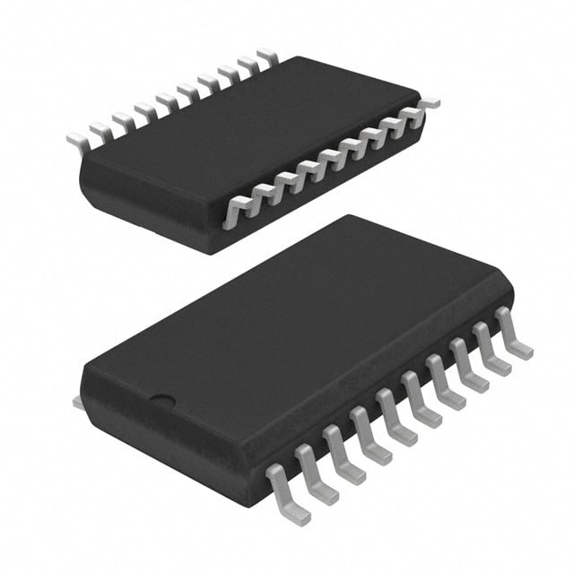
| 描述 | IC MCU 8BIT 4KB FLASH 20SOIC8位微控制器 -MCU 8051 4K FLASH 2.7 TO 5.5V 12MHZ 4V-5.5V |
| EEPROM容量 | - |
| 产品分类 | |
| I/O数 | 15 |
| 品牌 | Atmel |
| 产品手册 | |
| 产品图片 |
|
| rohs | 符合RoHS无铅 / 符合限制有害物质指令(RoHS)规范要求 |
| 产品系列 | 嵌入式处理器和控制器,微控制器 - MCU,8位微控制器 -MCU,Atmel AT89C4051-12SU89C |
| 数据手册 | |
| 产品型号 | AT89C4051-12SU |
| PCN设计/规格 | |
| RAM容量 | 128 x 8 |
| 产品培训模块 | http://www.digikey.cn/PTM/IndividualPTM.page?site=cn&lang=zhs&ptm=24997http://www.digikey.cn/PTM/IndividualPTM.page?site=cn&lang=zhs&ptm=26162http://www.digikey.cn/PTM/IndividualPTM.page?site=cn&lang=zhs&ptm=26159http://www.digikey.cn/PTM/IndividualPTM.page?site=cn&lang=zhs&ptm=26180 |
| 产品种类 | 8位微控制器 -MCU |
| 供应商器件封装 | 20-SOIC |
| 其它名称 | AT89C405112SU |
| 包装 | 管件 |
| 可编程输入/输出端数量 | 15 |
| 商标 | Atmel |
| 处理器系列 | AT89x |
| 外设 | 欠压检测/复位,LED,POR |
| 安装风格 | SMD/SMT |
| 定时器数量 | 2 Timer |
| 封装/外壳 | 20-SOIC(0.295",7.50mm 宽) |
| 封装/箱体 | SOIC |
| 工作温度 | -40°C ~ 85°C |
| 工作电源电压 | 2.7 V to 6 V |
| 工厂包装数量 | 38 |
| 振荡器类型 | 内部 |
| 接口类型 | UART |
| 数据RAM大小 | 128 B |
| 数据总线宽度 | 8 bit |
| 数据转换器 | - |
| 最大工作温度 | + 85 C |
| 最大时钟频率 | 24 MHz |
| 最小工作温度 | - 40 C |
| 标准包装 | 37 |
| 核心 | 8051 |
| 核心处理器 | 8051 |
| 核心尺寸 | 8-位 |
| 片上ADC | No |
| 电压-电源(Vcc/Vdd) | 2.7 V ~ 6 V |
| 电源电压-最大 | 6 V |
| 电源电压-最小 | 2.7 V |
| 程序存储器大小 | 4 kB |
| 程序存储器类型 | Flash |
| 程序存储容量 | 4KB(4K x 8) |
| 系列 | 89C |
| 输入/输出端数量 | 15 I/O |
| 连接性 | UART/USART |
| 速度 | 12MHz |


- 商务部:美国ITC正式对集成电路等产品启动337调查
- 曝三星4nm工艺存在良率问题 高通将骁龙8 Gen1或转产台积电
- 太阳诱电将投资9.5亿元在常州建新厂生产MLCC 预计2023年完工
- 英特尔发布欧洲新工厂建设计划 深化IDM 2.0 战略
- 台积电先进制程称霸业界 有大客户加持明年业绩稳了
- 达到5530亿美元!SIA预计今年全球半导体销售额将创下新高
- 英特尔拟将自动驾驶子公司Mobileye上市 估值或超500亿美元
- 三星加码芯片和SET,合并消费电子和移动部门,撤换高东真等 CEO
- 三星电子宣布重大人事变动 还合并消费电子和移动部门
- 海关总署:前11个月进口集成电路产品价值2.52万亿元 增长14.8%


PDF Datasheet 数据手册内容提取
Features • Compatible with MCS®51 Products (cid:129) 4K Bytes of Reprogrammable Flash Memory – Endurance: 10,000 Write/Erase Cycles (cid:129) 2.7V to 6V Operating Range (cid:129) Fully Static Operation: 0 Hz to 24 MHz (cid:129) Two-level Program Memory Lock (cid:129) 128 x 8-bit Internal RAM (cid:129) 15 Programmable I/O Lines 8-bit (cid:129) Two 16-bit Timer/Counters (cid:129) Six Interrupt Sources Microcontroller (cid:129) Programmable Serial UART Channel (cid:129) Direct LED Drive Outputs with 4K Bytes (cid:129) On-chip Analog Comparator (cid:129) Low-power Idle and Power-down Modes Flash (cid:129) Brown-out Detection (cid:129) Power-On Reset (POR) (cid:129) Green (Pb/Halide-free/RoHS Compliant) Packaging AT89C4051 1. Description The AT89C4051 is a low-voltage, high-performance CMOS 8-bit microcontroller with 4K bytes of Flash programmable and erasable read-only memory. The device is man- ufactured using Atmel’s high-density nonvolatile memory technology and is compatible with the industry-standard MCS-51 instruction set. By combining a versa- tile 8-bit CPU with Flash on a monolithic chip, the Atmel AT89C4051 is a powerful microcontroller which provides a highly-flexible and cost-effective solution to many embedded control applications. The AT89C4051 provides the following standard features: 4K bytes of Flash, 128 bytes of RAM, 15 I/O lines, two 16-bit timer/counters, a five-vector, two-level inter- rupt architecture, a full duplex serial port, a precision analog comparator, on-chip oscillator and clock circuitry. In addition, the AT89C4051 is designed with static logic for operation down to zero frequency and supports two software-selectable power saving modes. The Idle Mode stops the CPU while allowing the RAM, timer/counters, serial port and interrupt system to continue functioning. The power-down mode saves the RAM contents but freezes the oscillator disabling all other chip functions until the next hardware reset. 1001F–MICRO–6/08
2. Pin Configuration 2.1 PDIP/SOIC RST/VPP 1 20 VCC (RXD) P3.0 2 19 P1.7 (TXD) P3.1 3 18 P1.6 XTAL2 4 17 P1.5 XTAL1 5 16 P1.4 (INT0) P3.2 6 15 P1.3 (INT1) P3.3 7 14 P1.2 (TO) P3.4 8 13 P1.1 (AIN1) (T1) P3.5 9 12 P1.0 (AIN0) GND 10 11 P3.7 3. Block Diagram AT89C4051 2 1001F–MICRO–6/08
AT89C4051 4. Pin Description 4.1 VCC Supply voltage. 4.2 GND Ground. 4.3 Port 1 Port 1 is an 8-bit bi-directional I/O port. Port pins P1.2 to P1.7 provide internal pullups. P1.0 and P1.1 require external pullups. P1.0 and P1.1 also serve as the positive input (AIN0) and the neg- ative input (AIN1), respectively, of the on-chip precision analog comparator. The Port 1 output buffers can sink 20 mA and can drive LED displays directly. When 1s are written to Port 1 pins, they can be used as inputs. When pins P1.2 to P1.7 are used as inputs and are externally pulled low, they will source current (I ) because of the internal pullups. IL Port 1 also receives code data during Flash programming and verification. 4.4 Port 3 Port 3 pins P3.0 to P3.5, P3.7 are seven bi-directional I/O pins with internal pullups. P3.6 is hard-wired as an input to the output of the on-chip comparator and is not accessible as a gen- eral-purpose I/O pin. The Port 3 output buffers can sink 20 mA. When 1s are written to Port 3 pins they are pulled high by the internal pullups and can be used as inputs. As inputs, Port 3 pins that are externally being pulled low will source current (I ) because of the pullups. IL Port 3 also serves the functions of various special features of the AT89C4051 as listed below: Port Pin Alternate Functions P3.0 RXD (serial input port) P3.1 TXD (serial output port) P3.2 INT0 (external interrupt 0) P3.3 INT1 (external interrupt 1) P3.4 T0 (timer 0 external input) P3.5 T1 (timer 1 external input) Port 3 also receives some control signals for Flash programming and verification. 4.5 RST Reset input. All I/O pins are reset to 1s as soon as RST goes high. Holding the RST pin high for two machine cycles while the oscillator is running resets the device. Each machine cycle takes 12 oscillator or clock cycles. 4.6 XTAL1 Input to the inverting oscillator amplifier and input to the internal clock operating circuit. 3 1001F–MICRO–6/08
4.7 XTAL2 Output from the inverting oscillator amplifier. 5. Oscillator Characteristics XTAL1 and XTAL2 are the input and output, respectively, of an inverting amplifier which can be configured for use as an on-chip oscillator, as shown in Figure 5-1. Either a quartz crystal or ceramic resonator may be used. To drive the device from an external clock source, XTAL2 should be left unconnected while XTAL1 is driven as shown in Figure 5-2. There are no require- ments on the duty cycle of the external clock signal, since the input to the internal clocking circuitry is through a divide-by-two flip-flop, but minimum and maximum voltage high and low time specifications must be observed. Figure 5-1. Oscillator Connections Note: C1, C2 = 30 pF ± 10 pF for Crystals = 40 pF ± 10 pF for Ceramic Resonators Figure 5-2. External Clock Drive Configuration AT89C4051 4 1001F–MICRO–6/08
AT89C4051 6. Special Function Registers A map of the on-chip memory area called the Special Function Register (SFR) space is shown in the Table 6-1. Note that not all of the addresses are occupied, and unoccupied addresses may not be imple- mented on the chip. Read accesses to these addresses will in general return random data, and write accesses will have an indeterminate effect. User software should not write 1s to these unlisted locations, since they may be used in future products to invoke new features. In that case, the reset or inactive values of the new bits will always be 0. Table 6-1. AT89C4051 SFR Map and Reset Values 0F8H 0FFH B 0F0H 0F7H 00000000 0E8H 0EFH ACC 0E0H 0E7H 00000000 0D8H 0DFH PSW 0D0H 0D7H 00000000 0C8H 0CFH 0C0H 0C7H IP 0B8H 0BFH XXX00000 P3 0B0H 0B7H 11111111 IE 0A8H 0AFH 0XX00000 0A0H 0A7H SCON SBUF 98H 9FH 00000000 XXXXXXXX P1 90H 97H 11111111 TCON TMOD TL0 TL1 TH0 TH1 88H 8FH 00000000 00000000 00000000 00000000 00000000 00000000 SP DPL DPH PCON 80H 87H 00000111 00000000 00000000 0XXX0000 5 1001F–MICRO–6/08
7. Restrictions on Certain Instructions The AT89C4051 is an economical and cost-effective member of Atmel’s growing family of micro- controllers. It contains 4K bytes of Flash program memory. It is fully compatible with the MCS-51 architecture, and can be programmed using the MCS-51 instruction set. However, there are a few considerations one must keep in mind when utilizing certain instructions to program this device. All the instructions related to jumping or branching should be restricted such that the destination address falls within the physical program memory space of the device, which is 4K for the AT89C4051. This should be the responsibility of the software programmer. For example, LJMP 0FE0H would be a valid instruction for the AT89C4051 (with 4K of memory), whereas LJMP 1000H would not. 7.1 Branching Instructions LCALL, LJMP, ACALL, AJMP, SJMP, JMP @A+DPTR. These unconditional branching instruc- tions will execute correctly as long as the programmer keeps in mind that the destination branching address must fall within the physical boundaries of the program memory size (loca- tions 00H to FFFH for the 89C4051). Violating the physical space limits may cause unknown program behavior. CJNE [...], DJNZ [...], JB, JNB, JC, JNC, JBC, JZ, JNZ. With these conditional branching instructions the same rule above applies. Again, violating the memory boundaries may cause erratic execution. For applications involving interrupts, the normal interrupt service routine address locations of the 80C51 family architecture have been preserved. 7.2 MOVX-related Instructions, Data Memory The AT89C4051 contains 128 bytes of internal data memory. Thus, in the AT89C4051 the stack depth is limited to 128 bytes, the amount of available RAM. External DATA memory access is not supported in this device, nor is external Program memory execution. Therefore, no MOVX [...] instructions should be included in the program. A typical 80C51 assembler will still assemble instructions, even if they are written in violation of the restrictions mentioned above. It is the responsibility of the controller user to know the physi- cal features and limitations of the device being used and adjust the instructions used correspondingly. 8. Program Memory Lock Bits On the chip are two lock bits which can be left unprogrammed (U) or can be programmed (P) to obtain the additional features listed in the Table 8-1. Table 8-1. Lock Bit Protection Modes(1) Program Lock Bits LB1 LB2 Protection Type 1 U U No program lock features 2 P U Further programming of the Flash is disabled 3 P P Same as mode 2, also verify is disabled Note: 1. The Lock Bits can only be erased with the Chip Erase operation. AT89C4051 6 1001F–MICRO–6/08
AT89C4051 9. Idle Mode In idle mode, the CPU puts itself to sleep while all the on-chip peripherals remain active. The mode is invoked by software. The content of the on-chip RAM and all the special functions regis- ters remain unchanged during this mode. The idle mode can be terminated by any enabled interrupt or by a hardware reset. P1.0 and P1.1 should be set to “0” if no external pullups are used, or set to “1” if external pullups are used. It should be noted that when idle is terminated by a hardware reset, the device normally resumes program execution, from where it left off, up to two machine cycles before the internal reset algorithm takes control. On-chip hardware inhibits access to internal RAM in this event, but access to the port pins is not inhibited. To eliminate the possibility of an unexpected write to a port pin when Idle is terminated by reset, the instruction following the one that invokes Idle should not be one that writes to a port pin or to external memory. 10. Power-down Mode In the power-down mode the oscillator is stopped and the instruction that invokes power-down is the last instruction executed. The on-chip RAM and Special Function Registers retain their val- ues until the power-down mode is terminated. The only exit from power-down is a hardware reset. Reset redefines the SFRs but does not change the on-chip RAM. The reset should not be activated before V is restored to its normal operating level and must be held active long CC enough to allow the oscillator to restart and stabilize. P1.0 and P1.1 should be set to “0” if no external pullups are used, or set to “1” if external pullups are used. 11. Brown-out Detection When V drops below the detection threshold, all port pins (except P1.0 and P1.1) are weakly CC pulled high. When V goes back up again, an internal Reset is automatically generated after a CC delay of typically 15 msec. The nominal brown-out detection threshold is 2.1V ± 10%. V CC 2.1V 2.1V PORT PIN INTERNAL RESET 15 msec. 7 1001F–MICRO–6/08
12. Programming The Flash The AT89C4051 is shipped with the 4K bytes of on-chip PEROM code memory array in the erased state (i.e., contents = FFH) and ready to be programmed. The code memory array is pro- grammed one byte at a time. Once the array is programmed, to re-program any non-blank byte, the entire memory array needs to be erased electrically. Internal Address Counter: The AT89C4051 contains an internal PEROM address counter which is always reset to 000H on the rising edge of RST and is advanced by applying a positive going pulse to pin XTAL1. Programming Algorithm: To program the AT89C4051, the following sequence is recommended. 1. Power-up sequence: Apply power between VCCand GND pins Set RST and XTAL1 to GND 2. Set pin RST to “H” Set pin P3.2 to “H” 3. Apply the appropriate combination of “H” or “L” logic levels to pins P3.3, P3.4, P3.5, P3.7 to select one of the programming operations shown in the PEROM Programming Modes table. To Program and Verify the Array: 4. Apply data for Code byte at location 000H to P1.0 to P1.7. 5. Raise RST to 12V to enable programming. 6. Pulse P3.2 once to program a byte in the PEROM array or the lock bits. The byte-write cycle is self-timed and typically takes 1.2 ms. 7. To verify the programmed data, lower RST from 12V to logic “H” level and set pins P3.3 to P3.7 to the appropriate levels. Output data can be read at the port P1 pins. 8. To program a byte at the next address location, pulse XTAL1 pin once to advance the internal address counter. Apply new data to the port P1 pins. 9. Repeat steps 6 through 8, changing data and advancing the address counter for the entire 4K bytes array or until the end of the object file is reached. 10. Power-off sequence: set XTAL1 to “L” set RST to “L” Turn V power off CC Data Polling: The AT89C4051 features Data Polling to indicate the end of a write cycle. During a write cycle, an attempted read of the last byte written will result in the complement of the writ- ten data on P1.7. Once the write cycle has been completed, true data is valid on all outputs, and the next cycle may begin. Data Polling may begin any time after a write cycle has been initiated. Ready/Busy: The Progress of byte programming can also be monitored by the RDY/BSY output signal. Pin P3.1 is pulled low after P3.2 goes High during programming to indicate BUSY. P3.1 is pulled High again when programming is done to indicate READY. AT89C4051 8 1001F–MICRO–6/08
AT89C4051 Program Verify: If lock bits LB1 and LB2 have not been programmed code data can be read back via the data lines for verification: 1. Reset the internal address counter to 000H by bringing RST from “L” to “H”. 2. Apply the appropriate control signals for Read Code data and read the output data at the port P1 pins. 3. Pulse pin XTAL1 once to advance the internal address counter. 4. Read the next code data byte at the port P1 pins. 5. Repeat steps 3 and 4 until the entire array is read. The lock bits cannot be verified directly. Verification of the lock bits is achieved by observing that their features are enabled. Chip Erase: The entire PEROM array (4K bytes) and the two Lock Bits are erased electrically by using the proper combination of control signals and by holding P3.2 low for 10 ms. The code array is written with all “1”s in the Chip Erase operation and must be executed before any non- blank memory byte can be re-programmed. Reading the Signature Bytes: The signature bytes are read by the same procedure as a nor- mal verification of locations 000H, 001H, and 002H, except that P3.5 and P3.7 must be pulled to a logic low. The values returned are as follows. (000H) = 1EH indicates manufactured by Atmel (001H) = 41H indicates AT89C4051 13. Programming Interface Every code byte in the Flash array can be written and the entire array can be erased by using the appropriate combination of control signals. The write operation cycle is self-timed and once initiated, will automatically time itself to completion. Most major worldwide programming vendors offer support for the Atmel AT89 microcontroller series. Please contact your local programming vendor for the appropriate software revision. 13.1 Flash Programming Modes Mode RST/V P3.2/PROG P3.3 P3.4 P3.5 P3.7 PP Write Code Data(1)(3) 12V L H H H Read Code Data(1) H H L L H H Bit - 1 12V H H H H Write Lock Bit - 2 12V H H L L Chip Erase 12V (2) H L L L Read Signature Byte H H L L L L Notes: 1. The internal PEROM address counter is reset to 000H on the rising edge of RST and is advanced by a positive pulse at XTAL1 pin. 2. Chip Erase requires a 10-ms PROG pulse. 3. P3.1 is pulled Low during programming to indicate RDY/BSY. 9 1001F–MICRO–6/08
Figure 13-1. Programming the Flash Memory AT89C4051 P3.1 RDY/BSY PP Figure 13-2. Verifying the Flash Memory AT89C4051 AT89C4051 10 1001F–MICRO–6/08
AT89C4051 14. Flash Programming and Verification Characteristics T = 20°C to 30°C, V = 5.0 ± 10% A CC Symbol Parameter Min Max Units V Programming Enable Voltage 11.5 12.5 V PP I Programming Enable Current 250 µA PP t Data Setup to PROG Low 1.0 µs DVGL t Data Hold after PROG 1.0 µs GHDX t P3.4 (ENABLE) High to V 1.0 µs EHSH PP t V Setup to PROG Low 10 µs SHGL PP t V Hold after PROG 10 µs GHSL PP t PROG Width 1 110 µs GLGH t ENABLE Low to Data Valid 1.0 µs ELQV t Data Float after ENABLE 0 1.0 µs EHQZ t PROG High to BUSY Low 50 ns GHBL t Byte Write Cycle Time 2.0 ms WC t RDY/BSY\ to Increment Clock Delay 1.0 µs BHIH t Increment Clock High 200 ns IHIL Note: 1. Only used in 12-volt programming mode. 15. Flash Programming and Verification Waveforms 11 1001F–MICRO–6/08
16. Absolute Maximum Ratings* Operating Temperature.................................-55°C to +125°C *NOTICE: Stresses beyond those listed under “Absolute Maximum Ratings” may cause permanent dam- Storage Temperature.....................................-65°C to +150°C age to the device. This is a stress rating only and functional operation of the device at these or any Voltage on Any Pin other conditions beyond those indicated in the with Respect to Ground.....................................-1.0V to +7.0V operational sections of this specification is not implied. Exposure to absolute maximum rating Maximum Operating Voltage............................................6.6V conditions for extended periods may affect device reliability. DC Output Current......................................................25.0 mA 17. DC Characteristics T = -40°C to 85°C, V = 2.7V to 6.0V (unless otherwise noted) A CC Symbol Parameter Condition Min Max Units V Input Low-voltage -0.5 0.2 V - 0.1 V IL CC V Input High-voltage (Except XTAL1, RST) 0.2 V + 0.9 V + 0.5 V IH CC CC V Input High-voltage (XTAL1, RST) 0.7 V V + 0.5 V IH1 CC CC Output Low-voltage(1) I = 20 mA, V = 5V V OL CC 0.5 V OL (Ports 1, 3) I = 10 mA, V = 2.7V OL CC I = -80 µA, V = 5V ± 10% 2.4 V OH CC Output High-voltage V I = -30 µA 0.75 V V OH (Ports 1, 3) OH CC I = -12 µA 0.9 V V OH CC Logical 0 Input Current I V = 0.45V -50 µA IL (Ports 1, 3) IN Logical 1 to 0 Transition Current I V = 2V, V = 5V ± 10% -750 µA TL (Ports 1, 3) IN CC Input Leakage Current I 0 < V < V ±10 µA LI (Port P1.0, P1.1) IN CC V Comparator Input Offset Voltage V = 5V 20 mV OS CC Comparator Input Common V 0 V V CM Mode Voltage CC RRST Reset Pulldown Resistor 50 300 KΩ C Pin Capacitance Test Freq. = 1 MHz, T = 25°C 10 pF IO A Active Mode, 12 MHz, V = 6V/3V 15/5.5 mA CC Power Supply Current Idle Mode, 12 MHz, V = 6V/3V CC 5/1 mA ICC P1.0 & P1.1 = 0V or VCC V = 6V, P1.0 & P1.1 = 0V or V 20 µA Power-down Mode(2) CC CC V = 3V, P1.0 & P1.1 = 0V or V 5 µA CC CC Notes: 1. Under steady state (non-transient) conditions, I must be externally limited as follows: OL Maximum I per port pin: 20 mA OL Maximum total I for all output pins: 80 mA OL If I exceeds the test condition, V may exceed the related specification. Pins are not guaranteed to sink current greater OL OL than the listed test conditions. 2. Minimum V for Power-down is 2V. CC AT89C4051 12 1001F–MICRO–6/08
AT89C4051 18. External Clock Drive Waveforms 19. External Clock Drive V = 2.7V to 6.0V V = 4.0V to 6.0V CC CC Symbol Parameter Min Max Min Max Units 1/t Oscillator Frequency 0 12 0 24 MHz CLCL t Clock Period 83.3 41.6 ns CLCL t High Time 30 15 ns CHCX t Low Time 30 15 ns CLCX t Rise Time 20 20 ns CLCH t Fall Time 20 20 ns CHCL 13 1001F–MICRO–6/08
20. Serial Port Timing: Shift Register Mode Test Conditions V = 5.0V ± 20%; Load Capacitance = 80 pF CC 12 MHz Osc Variable Oscillator Symbol Parameter Min Max Min Max Units t Serial Port Clock Cycle Time 1.0 12t µs XLXL CLCL t Output Data Setup to Clock Rising Edge 700 10t -133 ns QVXH CLCL t Output Data Hold after Clock Rising Edge 50 2t -117 ns XHQX CLCL t Input Data Hold after Clock Rising Edge 0 0 ns XHDX t Clock Rising Edge to Input Data Valid 700 10t -133 ns XHDV CLCL 21. Shift Register Mode Timing Waveforms 22. AC Testing Input/Output Waveforms(1) Note: 1. AC Inputs during testing are driven at V - 0.5V for a logic 1 and 0.45V for a logic 0. Timing measurements are made at V CC IH min. for a logic 1 and V max. for a logic 0. IL 23. Float Waveforms(1) Note: 1. For timing purposes, a port pin is no longer floating when a 100 mV change from load voltage occurs. A port pin begins to float when 100 mV change from the loaded V /V level occurs. OH OL AT89C4051 14 1001F–MICRO–6/08
AT89C4051 24. I (Active Mode) Measurements CC AT89C4051 TYPICAL ICC-ACTIVE(85˚C) 20 Vcc=6.0V I 15 C Vcc=5.0V C 10 Vcc=3.0V m A 5 0 0 6 12 18 24 FREQUENCY(MHz) 25. I (Idle Mode) Measurements CC AT89C4051 TYPICAL ICC- IDLE(85˚C) 3 Vcc=6.0V I C 2 Vcc=5.0V C m 1 A Vcc=3.0V 0 0 3 6 9 12 FREQUENCY(MHz) 26. I (Power Down Mode) Measurements CC AT89C4051 TYPICAL ICCvs.VOLTAGE- POWERDOWN(85˚C) 20 I 15 C C 10 µ A 5 0 3.0V 4.0V 5.0V 6.0V VccVOLTAGE Notes: 1. XTAL1 tied to GND 2. P.1.0 and P1.1 = V or GND CC 3. Lock bits programmed 15 1001F–MICRO–6/08
27. Ordering Information 27.1 Green Package Option (Pb/Halide-free) Speed Power (MHz) Supply Ordering Code Package Operation Range AT89C4051-12PU 20P3 Industrial 12 2.7V to 6.0V AT89C4051-12SU 20S (-40°C to 85°C) AT89C4051-24PU 20P3 Industrial 24 4.0V to 6.0V AT89C4051-24SU 20S (-40°C to 85°C) Package Type 20P3 20-lead, 0.300” Wide, Plastic Dual In-line Package (PDIP) 20S 20-lead, 0.300” Wide, Plastic Gull Wing Small Outline (SOIC) AT89C4051 16 1001F–MICRO–6/08
AT89C4051 28. Package Information 28.1 20P3 – PDIP D PIN 1 E1 A SEATING PLANE A1 L B B1 e E COMMON DIMENSIONS (Unit of Measure = mm) C SYMBOL MIN NOM MAX NOTE eC eB A – – 5.334 A1 0.381 – – D 24.892 – 26.924 Note 2 E 7.620 – 8.255 E1 6.096 – 7.112 Note 2 B 0.356 – 0.559 B1 1.270 – 1.551 Notes: 1.This package conforms to JEDEC reference MS-001, Variation AD. 2.Dimensions D and E1 do not include mold Flash or Protrusion. L 2.921 – 3.810 Mold Flash or Protrusion shall not exceed 0.25 mm (0.010"). C 0.203 – 0.356 eB – – 10.922 eC 0.000 – 1.524 e 2.540 TYP 1/23/04 TITLE DRAWING NO. REV. 2325 Orchard Parkway 20P3, 20-lead (0.300"/7.62 mm Wide) Plastic Dual R San Jose, CA 95131 Inline Package (PDIP) 20P3 D 17 1001F–MICRO–6/08
28.2 20S – SOIC AT89C4051 18 1001F–MICRO–6/08
Headquarters International Atmel Corporation Atmel Asia Atmel Europe Atmel Japan 2325 Orchard Parkway Room 1219 Le Krebs 9F, Tonetsu Shinkawa Bldg. San Jose, CA 95131 Chinachem Golden Plaza 8, Rue Jean-Pierre Timbaud 1-24-8 Shinkawa USA 77 Mody Road Tsimshatsui BP 309 Chuo-ku, Tokyo 104-0033 Tel: 1(408) 441-0311 East Kowloon 78054 Saint-Quentin-en- Japan Fax: 1(408) 487-2600 Hong Kong Yvelines Cedex Tel: (81) 3-3523-3551 Tel: (852) 2721-9778 France Fax: (81) 3-3523-7581 Fax: (852) 2722-1369 Tel: (33) 1-30-60-70-00 Fax: (33) 1-30-60-71-11 Product Contact Web Site Technical Support Sales Contact www.atmel.com mcu@atmel.com www.atmel.com/contacts Literature Requests www.atmel.com/literature Disclaimer: The information in this document is provided in connection with Atmel products. No license, express or implied, by estoppel or otherwise, to any intellectual property right is granted by this document or in connection with the sale of Atmel products. EXCEPT AS SET FORTH IN ATMEL’S TERMS AND CONDI- TIONS OF SALE LOCATED ON ATMEL’S WEB SITE, ATMEL ASSUMES NO LIABILITY WHATSOEVER AND DISCLAIMS ANY EXPRESS, IMPLIED OR STATUTORY WARRANTY RELATING TO ITS PRODUCTS INCLUDING, BUT NOT LIMITED TO, THE IMPLIED WARRANTY OF MERCHANTABILITY, FITNESS FOR A PARTICULAR PURPOSE, OR NON-INFRINGEMENT. IN NO EVENT SHALL ATMEL BE LIABLE FOR ANY DIRECT, INDIRECT, CONSEQUENTIAL, PUNITIVE, SPECIAL OR INCIDEN- TAL DAMAGES (INCLUDING, WITHOUT LIMITATION, DAMAGES FOR LOSS OF PROFITS, BUSINESS INTERRUPTION, OR LOSS OF INFORMATION) ARISING OUT OF THE USE OR INABILITY TO USE THIS DOCUMENT, EVEN IF ATMEL HAS BEEN ADVISED OF THE POSSIBILITY OF SUCH DAMAGES. Atmel makes no representations or warranties with respect to the accuracy or completeness of the contents of this document and reserves the right to make changes to specifications and product descriptions at any time without notice. Atmel does not make any commitment to update the information contained herein. Unless specifically provided otherwise, Atmel products are not suitable for, and shall not be used in, automotive applications. Atmel’s products are not intended, authorized, or warranted for use as components in applications intended to support or sustain life. © 2008 Atmel Corporation. All rights reserved. Atmel®, logo and combinations thereof, and others are registered trademarks or trademarks of Atmel Corporation or its subsidiaries. Other terms and product names may be trademarks of others. 1001F–MICRO–6/08
Mouser Electronics Authorized Distributor Click to View Pricing, Inventory, Delivery & Lifecycle Information: M icrochip: AT89C4051-12PU AT89C4051-24PU AT89C4051-12SU AT89C4051-24SU