ICGOO在线商城 > 集成电路(IC) > 嵌入式 - 微控制器 > AT80C51RD2-3CSUM
 Datasheet下载
- 型号: AT80C51RD2-3CSUM
- 制造商: Atmel
- 库位|库存: xxxx|xxxx
- 要求:
| 数量阶梯 | 香港交货 | 国内含税 |
| +xxxx | $xxxx | ¥xxxx |
查看当月历史价格
查看今年历史价格
AT80C51RD2-3CSUM产品简介:
ICGOO电子元器件商城为您提供AT80C51RD2-3CSUM由Atmel设计生产,在icgoo商城现货销售,并且可以通过原厂、代理商等渠道进行代购。 AT80C51RD2-3CSUM价格参考。AtmelAT80C51RD2-3CSUM封装/规格:嵌入式 - 微控制器, 80C51 微控制器 IC 80C 8-位 40MHz ROMless 40-PDIL。您可以下载AT80C51RD2-3CSUM参考资料、Datasheet数据手册功能说明书,资料中有AT80C51RD2-3CSUM 详细功能的应用电路图电压和使用方法及教程。
AT80C51RD2-3CSUM 是由 Microchip Technology 提供的一款基于 8051 架构的增强型微控制器,属于嵌入式 - 微控制器类别。该型号在多种应用场景中具有广泛的应用潜力,以下是其主要应用场景:

 1. 工业自动化
   - 用于控制和监测工业设备,如电机驱动、传感器数据采集和处理。
   - 支持实时控制任务,例如温度、压力或液位监控。
   - 在生产线中实现简单的逻辑控制和数据传输。

 2. 消费电子
   - 应用于家用电器(如洗衣机、冰箱、空调等)的主控单元,负责运行模式切换、能耗管理等功能。
   - 用于遥控器、电子玩具和其他便携式电子设备中的嵌入式控制。

 3. 医疗设备
   - 适用于便携式健康监测设备(如血压计、血糖仪)的数据处理与显示。
   - 提供低功耗解决方案,延长电池寿命。

 4. 通信与网络
   - 用作小型通信模块的核心处理器,支持串口通信、UART 或 I2C 数据交换。
   - 在 Modem 或简易网关设备中执行协议解析和数据转发。

 5. 汽车电子
   - 用于车窗升降、雨刷控制、座椅调节等简单车载系统。
   - 实现基本的故障诊断功能。

 6. 教育与开发平台
   - 作为教学实验板的核心芯片,帮助学生学习单片机编程和硬件设计。
   - 提供丰富的外设资源(如定时器、中断、I/O端口),便于开发原型项目。

 特性优势:
- 高性能:相比传统 8051,AT80C51RD2 提供更高的时钟频率和更强的计算能力。
- 低功耗:适合对能效要求较高的场景。
- 高集成度:内置 Flash 存储器、EEPROM 和 RAM,减少外部元件需求。
- 易用性:兼容标准 8051 指令集,便于移植现有代码。

综上所述,AT80C51RD2-3CSUM 微控制器凭借其强大的性能和灵活性,可广泛应用于工业、消费、医疗等多个领域,满足多样化的嵌入式需求。
| 参数 | 数值 |
| A/D位大小 | No ADC |
| 产品目录 | 集成电路 (IC)半导体 |
| 描述 | IC MCU 8BIT ROMLESS 40DIP8位微控制器 -MCU MCU 8-BIT AT80 CISC ROMless 3-5V |
| EEPROM容量 | - |
| 产品分类 | |
| I/O数 | 32 |
| 品牌 | Atmel |
| 产品手册 | |
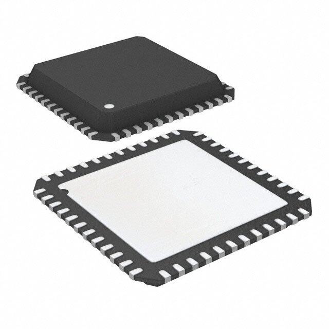
| 产品图片 |
|
| rohs | 符合RoHS无铅 / 符合限制有害物质指令(RoHS)规范要求 |
| 产品系列 | 嵌入式处理器和控制器,微控制器 - MCU,8位微控制器 -MCU,Atmel AT80C51RD2-3CSUM80C |
| 数据手册 | |
| 产品型号 | AT80C51RD2-3CSUM |
| RAM容量 | 1K x 8 |
| 产品培训模块 | http://www.digikey.cn/PTM/IndividualPTM.page?site=cn&lang=zhs&ptm=26162http://www.digikey.cn/PTM/IndividualPTM.page?site=cn&lang=zhs&ptm=26159http://www.digikey.cn/PTM/IndividualPTM.page?site=cn&lang=zhs&ptm=26180 |
| 产品种类 | 8位微控制器 -MCU |
| 供应商器件封装 | * |
| 其它名称 | AT80C51RD23CSUM |
| 包装 | 管件 |
| 可编程输入/输出端数量 | 32 |
| 商标 | Atmel |
| 处理器系列 | AT80x |
| 外设 | POR,PWM,WDT |
| 安装风格 | Through Hole |
| 定时器数量 | 3 Timer |
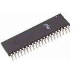
| 封装/外壳 | 40-DIP(0.600",15.24mm) |
| 封装/箱体 | PDIL-40 |
| 工作温度 | -40°C ~ 85°C |
| 工作电源电压 | 2.7 V to 5.5 V |
| 工厂包装数量 | 216 |
| 振荡器类型 | 内部 |
| 接口类型 | SPI, UART |
| 数据RAM大小 | 1280 B |
| 数据总线宽度 | 8 bit |
| 数据转换器 | - |
| 最大工作温度 | + 70 C |
| 最大时钟频率 | 60 MHz |
| 最小工作温度 | 0 C |
| 标准包装 | 216 |
| 核心 | 8051 |
| 核心处理器 | 80C51 |
| 核心尺寸 | 8-位 |
| 片上ADC | No |
| 电压-电源(Vcc/Vdd) | 4.5 V ~ 5.5 V |
| 电源电压-最大 | 5.5 V |
| 电源电压-最小 | 2.7 V |
| 程序存储器类型 | ROMLess |
| 程序存储容量 | - |
| 系列 | 80C |
| 输入/输出端数量 | 32 I/O |
| 连接性 | UART/USART |
| 速度 | 40MHz |


PDF Datasheet 数据手册内容提取
Features • 80C52 Compatible – Four 8-bit I/O Ports – Three 16-bit Timer/Counters – 256 Bytes Scratch Pad RAM – 8 Interrupt Sources with 4 Priority Levels – Dual Data Pointer (cid:129) Variable Length MOVX for Slow RAM/Peripherals (cid:129) High-speed Architecture 80C51 High – 10 to 40 MHz in Standard Mode (cid:129) 16K/32K Bytes On-Chip ROM Program Performance (cid:129) AT80C51RD2 ROMless Versions (cid:129) On-Chip 1024 bytes Expanded RAM (XRAM) ROM 8-bit – Software Selectable Size (0, 256, 512, 768, 1024 bytes) – 256 Bytes Selected at Reset Microcontroller (cid:129) Keyboard Interrupt Interface on Port P1 (cid:129) 8-bit Clock Prescaler (cid:129) 64K Program and Data Memory Spaces AT80C51RD2 (cid:129) Improved X2 Mode with Independant Selection for CPU and Each Peripheral (cid:129) Programmable Counter Array 5 Channels with: – High-speed Output – Compare/Capture – Pulse Width Modulator – Watchdog Timer Capabilities (cid:129) Asynchronous Port Reset (cid:129) Full Duplex Enhanced UART (cid:129) Dedicated Baud Rate Generator for UART (cid:129) Low EMI (Inhibit ALE) (cid:129) Hardware Watchdog Timer (One-time Enabled with Reset-out) (cid:129) Power Control Modes – Idle Mode – Power-down Mode – Power-off Flag (cid:129) Power Supply: 2.7V to 5.5V (cid:129) Temperature Ranges: Commercial (0 to +70°C) and Industrial (-40°C to +85°C) (cid:129) Packages: PDIL40, PLCC44, VQFP44
1. Description AT80C51RD2 microcontrollers are high performance versions of the 80C51 8-bit microcontrollers. The microcontrollers retain all features of the Atmel 80C52 with 256 bytes of internal RAM, a 7- source 4-level interrupt controller and three timer/counters. In addition, the microcontrollers have a Programmable Counter Array, an XRAM of 1024 byte, a Hardware Watchdog Timer, a Keyboard Interface, a more versatile serial channel that facilitates multiprocessor communication (EUART) and a speed improvement mechanism (X2 mode). The microcontrollers have 2 software-selectable modes of reduced activity and 8 bit clock pres- caler for further reduction in power consumption. In Idle mode, the CPU is frozen while the peripherals and the interrupt system are still operating. In the Power-down mode, the RAM is saved and all other functions are inoperative. Table 1. Memory Size ROM (Bytes) XRAM (Bytes) TOTAL RAM (Bytes) I/O AT80C51RD2 ROMless 1024 1280 32 2. Block Diagram RxD TxD VCC Vss ECI PCA T2EX T2 (2)(2) (1) (1)(1) (1) XTAL1 XTAL2 EUART RAM XRAM BR+G 256x8 1Kx8 PCA Timer2 ALE/PROG C51 PSEN CORE IB-bus CPU EA RD (2) Timer 0 INT Parallel I/O Ports & Ext. Bus Watch Key Timer 1 Ctrl Dog Board WR (2) Port 0Port 1Port 2Port 3 (2)(2) (2)(2) ET T0 T1 T0 T1 P0 P1 P2 P3 S N N E I I R Notes: 1. Alternate function of Port 1 2. Alternate function of Port 3 AT80C51RD2 2 4113D–8051–01/09
AT80C51RD2 3. Pin Configurations P1.0/T2 1 40 VCC P1.1/T2EX 2 39 P0.0/AD0 P1.2/ECI 3 38 P0.1/AD1 P1.3CEX0 4 37 P0.2/AD2 P1.4/CEX1 5 36 P0.3/AD3 P1.5/CEX2 6 35 P0.4/AD4 P1.6/CEX3 7 34 P0.5/AD5 P1.7CEX4 8 33 P0.6/AD6 RST 9 32 P0.7/AD7 P3.0/RxD 10 31 EA P3.1/TxD 11 PDIL40 30 ALE/PROG PP33P..233//.II4NN/TTT010 111432 222987 PPPS22..E76N//AADD1154 P1.4/CEX1 P1.3/CEX0 P1.2/ECI P1.1/T2EX P1.0/T2 NIC* VCC P0.0/AD0 P0.1/AD1 P0.2/AD2 P0.3/AD3 P2.5/AD13 P3.5/T1 15 26 6 5 4 3 2 1 4443424140 P3.6/WR 16 25 P2.4/AD12 P2.3/AD11 P1.5/CEX2 7 39 P0.4/AD4 P3XX.TT7AA/RLLD21 111789 222432 PP22..12//AADD910 PP11..67//CCREESXxT43 1890 333687 PPP000...657///AAADDD657 VSS 20 21 P2.0/AD8 P3.0/RxD 11 35 EA NIC* 12 PLCC44 34 NIC* P3.1/TxD 13 33 ALE/PROG P3.2/INT0 14 32 PSEN P3.3/INT1 15 31 P2.7/A15 P3.4/T0 16 30 P2.6/A14 P3.5/T1 17 29 P2.5/A13 1819202122232425262728 P1.4/CEX1 P1.3/CEX0 P1.2/ECI P1.1/T2EX P1.0/T2 NIC* VCC P0.0/AD0 P0.1/AD1 P0.2/AD2 P0.3/AD3 P3.6/WR P3.7/RD XTAL2 XTAL1 VSS NIC* P2.0/A8 P2.1/A9 P2.2/A10 P2.3/A11 P2.4/A12 444 34 24 14 03 93837363534 P1.5/CEX2 1 33 P0.4/AD4 P1.6/CEX3 2 32 P0.5/AD5 P1.7/CEX4 3 31 P0.6/AD6 RST 4 30 P0.7/AD7 P3.0/RxD 5 29 EA NIC* 6 VQFP44 1.4 28 NIC* P3.1/TxD 7 27 ALE/PROG P3.2/INT0 8 26 PSEN P3.3/INT1 9 25 P2.7/A15 P3.4/T0 10 24 P2.6/A14 P3.5/T1 11 23 P2.5/A13 1213141516171819202122 P3.6/WR P3.7/RD XTAL2 XTAL1 VSS NIC* P2.0/A8 P2.1/A9 P2.2/A10 P2.3/A11 P2.4/A12 *NIC: No Internal Connection 3 4113D–8051–01/09
Table 3-1. Pin Description Pin Number Mnemonic DIL PLCC44 VQFP44 1.4 Type Name and Function V 20 22 16 I Ground: 0V reference SS Power Supply: This is the power supply voltage for normal, idle and power-down V 40 44 38 I CC operation P0.0 - P0.7 39 - 32 43 - 36 37 - 30 I/O Port 0: Port 0 is an open-drain, bi-directional I/O port. Port 0 pins that have 1s written to them float and can be used as high impedance inputs. Port 0 must be polarized to V or V in order to prevent any parasitic current consumption. Port CC SS 0 is also the multiplexed low-order address and data bus during access to external program and data memory. In this application, it uses strong internal pull-up when emitting 1s. Port 0 also inputs the code bytes during EPROM programming. External pull-ups are required during program verification during which P0 outputs the code bytes. P1.0 - P1.7 1 - 8 2 - 9 40 - 44 I/O Port 1: Port 1 is an 8-bit bi-directional I/O port with internal pull-ups. Port 1 pins 1 - 3 that have 1s written to them are pulled high by the internal pull-ups and can be used as inputs. As inputs, Port 1 pins that are externally pulled low will source current because of the internal pull-ups. Port 1 also receives the low-order address byte during memory programming and verification. Alternate functions for T89C51RB2/RC2 Port 1 include: 1 2 40 I/O P1.0: Input/Output I/O T2 (P1.0): Timer/Counter 2 external count input/Clockout 2 3 41 I/O P1.1: Input/Output I T2EX: Timer/Counter 2 Reload/Capture/Direction Control 3 4 42 I/O P1.2: Input/Output I ECI: External Clock for the PCA 4 5 43 I/O P1.3: Input/Output I/O CEX0: Capture/Compare External I/O for PCA module 0 5 6 44 I/O P1.4: Input/Output I/O CEX1: Capture/Compare External I/O for PCA module 1 6 7 1 I/O P1.5: Input/Output I/O CEX2: Capture/Compare External I/O for PCA module 2 7 8 2 I/O P1.6: Input/Output I/O CEX3: Capture/Compare External I/O for PCA module 3 8 9 3 I/O P1.7: Input/Output: I/O CEX4: Capture/Compare External I/O for PCA module 4 Crystal 1: Input to the inverting oscillator amplifier and input to the internal clock XTAL1 19 21 15 I generator circuits. XTAL2 18 20 14 O Crystal 2: Output from the inverting oscillator amplifier AT80C51RD2 4 4113D–8051–01/09
AT80C51RD2 Table 3-1. Pin Description (Continued) Pin Number Mnemonic DIL PLCC44 VQFP44 1.4 Type Name and Function P2.0 - P2.7 21 - 28 24 - 31 18 - 25 I/O Port 2: Port 2 is an 8-bit bi-directional I/O port with internal pull-ups. Port 2 pins that have 1s written to them are pulled high by the internal pull-ups and can be used as inputs. As inputs, Port 2 pins that are externally pulled low will source current because of the internal pull-ups. Port 2 emits the high-order address byte during fetches from external program memory and during accesses to external data memory that use 16-bit addresses (MOVX @DPTR). In this application, it uses strong internal pull-ups emitting 1s. During accesses to external data memory that use 8-bit addresses (MOVX @Ri), Port 2 emits the contents of the P2 SFR. Some Port 2 pins receive the high order address bits during ROM reading and verification: P2.0 to P2.5 for 16 KB devices P2.0 to P2.6 for 32 KB devices P3.0 - P3.7 10 - 17 11, 5, I/O Port 3: Port 3 is an 8-bit bi-directional I/O port with internal pull-ups. Port 3 pins 13 - 19 7 - 13 that have 1s written to them are pulled high by the internal pull-ups and can be used as inputs. As inputs, Port 3 pins that are externally pulled low will source current because of the internal pull-ups. Port 3 also serves the special features of the 80C51 family, as listed below. 10 11 5 I RXD (P3.0): Serial input port 11 13 7 O TXD (P3.1): Serial output port 12 14 8 I INT0 (P3.2): External interrupt 0 13 15 9 I INT1 (P3.3): External interrupt 1 14 16 10 I T0 (P3.4): Timer 0 external input 15 17 11 I T1 (P3.5): Timer 1 external input 16 18 12 O WR (P3.6): External data memory write strobe 17 19 13 O RD (P3.7): External data memory read strobe Reset: A high on this pin for two machine cycles while the oscillator is running, resets the device. An internal diffused resistor to V permits a power-on reset RST 9 10 4 I/O SS using only an external capacitor to V . This pin is an output when the hardware CC watchdog forces a system reset. ALE/PROG 30 33 27 O (I) Address Latch Enable/Program Pulse: Output pulse for latching the low byte of the address during an access to external memory. In normal operation, ALE is emitted at a constant rate of 1/6 (1/3 in X2 mode) the oscillator frequency, and can be used for external timing or clocking. Note that one ALE pulse is skipped during each access to external data memory. This pin is also the program pulse input (PROG) during Flash programming. ALE can be disabled by setting SFR’s AUXR.0 bit. With this bit set, ALE will be inactive during internal fetches. PSEN 29 32 26 O Program Strobe Enable: The read strobe to external program memory. When executing code from the external program memory, PSEN is activated twice each machine cycle, except that two PSEN activations are skipped during each access to external data memory. PSEN is not activated during fetches from internal program memory. External Access Enable: EA must be externally held low to enable the device to EA 31 35 29 I fetch code from external program memory locations. If security level 1 is programmed, EA will be internally latched on Reset. 5 4113D–8051–01/09
4. SFR Mapping The Special Function Registers (SFRs) of the microcontroller fall into the following categories: (cid:129) C51 core registers: ACC, B, DPH, DPL, PSW, SP (cid:129) I/O port registers: P0, P1, P2, P3 (cid:129) Timer registers: T2CON, T2MOD, TCON, TH0, TH1, TH2, TMOD, TL0, TL1, TL2, RCAP2L, RCAP2H (cid:129) Serial I/O port registers: SADDR, SADEN, SBUF, SCON (cid:129) PCA (Programmable Counter Array) registers: CCON, CCAPMx, CL, CH, CCAPxH, CCAPxL (x: 0 to 4) (cid:129) Power and clock control registers: PCON (cid:129) Hardware Watchdog Timer registers: WDTRST, WDTPRG (cid:129) Interrupt system registers: IE0, IPL0, IPH0, IE1, IPL1, IPH1 (cid:129) Keyboard Interface registers: KBE, KBF, KBLS (cid:129) BRG (Baud Rate Generator) registers: BRL, BDRCON (cid:129) Clock Prescaler register: CKRL (cid:129) Others: AUXR, AUXR1, CKCON0, CKCON1 AT80C51RD2 6 4113D–8051–01/09
AT80C51RD2 Table 3 shows all SFRs with their address and their reset value. Table 4-1. SFR Mapping Bit Addressable Non-bit Addressable 0/8 1/9 2/A 3/B 4/C 5/D 6/E 7/F F8h CH CCAP0H CCAP1H CCAPL2H CCAPL3H CCAPL4H FFh 0000 0000 XXXX XXXX XXXX XXXX XXXX XXXX XXXX XXXX XXXX XXXX F0h B F7h 0000 0000 E8h CL CCAP0L CCAP1L CCAPL2L CCAPL3L CCAPL4L EFh 0000 0000 XXXX XXXX XXXX XXXX XXXX XXXX XXXX XXXX XXXX XXXX E0h ACC E7h 0000 0000 D8h CCON CMOD CCAPM0 CCAPM1 CCAPM2 CCAPM3 CCAPM4 DFh 00X0 0000 00XX X000 X000 0000 X000 0000 X000 0000 X000 0000 X000 0000 D0h PSW D7h 0000 0000 C8h T2CON T2MOD RCAP2L RCAP2H TL2 TH2 CFh 0000 0000 XXXX XX00 0000 0000 0000 0000 0000 0000 0000 0000 C0h C7h B8h IPL0 SADEN BFh X000 000 0000 0000 B0h P3 IE1 IPL1 IPH1 IPH0 B7h 1111 1111 XXXX XXX0b XXXX XXX0b XXXX XXX0b X000 0000 A8h IE0 SADDR AFh 0000 0000 0000 0000 A0h P2 AUXR1 WDTRST WDTPRG A7h 1111 1111 XXXX XXX0 XXXX XXXX XXXX X000 98h SCON SBUF BRL BDRCON KBLS KBE KBF 9Fh 0000 0000 XXXX XXXX 0000 0000 XXX0 0000 0000 0000 0000 0000 0000 0000 90h P1 CKRL 97h 1111 1111 1111 1111 88h TCON TMOD TL0 TL1 TH0 TH1 AUXR CKCON0 8Fh 0000 0000 0000 0000 0000 0000 0000 0000 0000 0000 0000 0000 XX0X 0000 0000 0000 80h P0 SP DPL DPH PCON 87h 1111 1111 0000 0111 0000 0000 0000 0000 00X1 0000 0/8 1/9 2/A 3/B 4/C 5/D 6/E 7/F Reserved 7 4113D–8051–01/09
5. Oscillators 5.1 Overview One oscillator is available for CPU: (cid:129) OSC used for high frequency (3 MHz to 40 MHz) In order to optimize the power consumption and the execution time needed for a specific task, an internal prescaler feature has been implemented between the selected oscillator and the CPU. 5.2 Registers Table 5-1. Clock Reload Register 7 6 5 4 3 2 1 0 - - - - - - - - Bit Bit Number Mnemonic Description 7:0 CKRL Clock Reload Register: Prescaler value Reset Value = 1111 1111b Not bit addressable 5.2.1 Prescaler Divider A hardware RESET puts the prescaler divider in the following state: (cid:129) CKRL = FFh: F = F = F /2 (Standard C51 feature) CLK CPU CLK PERIPH OSC KS signal selects OSC: F = F CLK OUT OSC (cid:129) Any value between FFh down to 00h can be written by software into CKRL register in order to divide frequency of the selected oscillator: – CKRL = 00h: minimum frequency F = F = F /1020 (Standard Mode) CLK CPU CLK PERIPH OSC F = F = F /510 (X2 Mode) CLK CPU CLK PERIPH OSC – CKRL = FFh: maximum frequency F = F = F /2 (Standard Mode) CLK CPU CLK PERIPH OSC F = F = F (X2 Mode) CLK CPU CLK PERIPH OSC – F and F CLK CPU CLK PERIPH In X2 mode: F F =F = ---------------------O----S---C------------------ CPU CLKPERIPH 2×(255–CKRL) F In X1 mode: F =F = --------------------O---S---C---A----------------- CPU CLKPERIPH 4×(255–CKRL) AT80C51RD2 8 4113D–8051–01/09
AT80C51RD2 6. Enhanced Features In comparison to the original 80C52, the microcontrollers implement the following new features: (cid:129) X2 option (cid:129) Dual Data Pointer (cid:129) Extended RAM (cid:129) Programmable Counter Array (PCA) (cid:129) Hardware Watchdog (cid:129) 4-level Interrupt Priority System (cid:129) Power-off Flag (cid:129) Power On Reset (cid:129) ONCE mode (cid:129) ALE disabling (cid:129) Some enhanced features are also located in the UART and the Timer 2 6.1 X2 Feature and OSC Clock Generation The microcontroller core needs only 6 clock periods per machine cycle. This feature called ”X2” provides the following advantages: (cid:129) Divides frequency crystals by 2 (cheaper crystals) while keeping same CPU power. (cid:129) Saves power consumption while keeping same CPU power (oscillator power saving). (cid:129) Saves power consumption by dividing dynamically the operating frequency by 2 in operating and idle modes. (cid:129) Increases CPU power by 2 while keeping same crystal frequency. In order to keep the original C51 compatibility, a divider by 2 is inserted between the XTAL1 sig- nal and the main clock input of the core (phase generator). This divider may be disabled by software. 6.1.1 Description The clock for the whole circuit and peripherals is first divided by two before being used by the CPU core and the peripherals. This allows any cyclic ratio to be accepted on XTAL1 input. In X2 mode, as this divider is bypassed, the signals on XTAL1 must have a cyclic ratio between 40 to 60%. Figure 6-1 shows the clock generation block diagram. X2 bit is validated on the rising edge of the XTAL1 ÷ 2 to avoid glitches when switching from X2 to standard mode. Figure 6-2 shows the switching mode waveforms. Figure 6-1. Clock Generation Diagram CKRL F XTAL1:2 OSC CLK Periph XTAL1 2 0 8-bit Prescaler FXTAL 1 CLK CPU Idle X2 CKCON0 9 4113D–8051–01/09
Figure 6-2. Mode Switching Waveforms XTAL1 XTAL1:2 X2 Bit F CPU Block OSC STD Mode X2 Mode STD Mode The X2 bit in the CKCON0 register (see Table6-1) allows to switch from 12 clock periods per instruction to 6 clock periods and vice versa. At reset, the speed is set according to X2 bit of Hardware Config Byte (HCB). By default, Standard mode is activated. Setting the X2 bit acti- vates the X2 feature (X2 mode). The T0X2, T1X2, T2X2, UARTX2, PCAX2 and WDX2 bits in the CKCON0 register (Table 6-1) allow to switch from standard peripheral speed (12 clock periods per peripheral clock cycle) to fast peripheral speed (6 clock periods per peripheral clock cycle). These bits are active only in X2 mode. Table 6-1. CKCON0 Register CKCON0 - Clock Control Register (8Fh) 7 6 5 4 3 2 1 0 - WDX2 PCAX2 SIX2 T2X2 T1X2 T0X2 X2 Bit Bit Number Mnemonic Description Reserved 7 - Do not set this bit. Watchdog clock (This control bit is validated when the CPU clock X2 is set; when X2 is low, this bit has no effect). 6 WDX2 Cleared to select 6 clock periods per peripheral clock cycle. Set to select 12 clock periods per peripheral clock cycle. AT80C51RD2 10 4113D–8051–01/09
AT80C51RD2 Bit Bit Number Mnemonic Description Programmable Counter Array clock (This control bit is validated when the CPU clock X2 is set; when X2 is low, this bit has no effect). 5 PCAX2 Cleared to select 6 clock periods per peripheral clock cycle. Set to select 12 clock periods per peripheral clock cycle. Enhanced UART clock (Mode 0 and 2) (This control bit is validated when the CPU clock X2 is set; when X2 is low, this bit has no effect). 4 SIX2 Cleared to select 6 clock periods per peripheral clock cycle. Set to select 12 clock periods per peripheral clock cycle. Timer 2 clock (This control bit is validated when the CPU clock X2 is set; when X2 is low, this bit has no effect). 3 T2X2 Cleared to select 6 clock periods per peripheral clock cycle. Set to select 12 clock periods per peripheral clock cycle. Timer 1 clock (This control bit is validated when the CPU clock X2 is set; when X2 is low, this bit has no effect). 2 T1X2 Cleared to select 6 clock periods per peripheral clock cycle. Set to select 12 clock periods per peripheral clock cycle Timer 0 clock (This control bit is validated when the CPU clock X2 is set; when X2 is low, this bit has no effect). 1 T0X2 Cleared to select 6 clock periods per peripheral clock cycle. Set to select 12 clock periods per peripheral clock cycle CPU clock Cleared to select 12 clock periods per machine cycle (STD mode) for CPU and all the peripherals. 0 X2 Set to select 6clock periods per machine cycle (X2 mode) and to enable the individual peripherals "X2" bits. Programmed by hardware after Power-up regarding Hardware Config Byte (HCB). Reset Value = 0000 000’HCB.X2’b (see Hardware Config Byte) Not bit addressable 11 4113D–8051–01/09
7. Dual Data Pointer Register The additional data pointer can be used to speed up code execution and reduce code size. The dual DPTR structure is a way by which the chip will specify the address of an external data memory location. There are two 16-bit DPTR registers that address the external memory, and a single bit called DPS = AUXR1.0 (see Table 7-1) that allows the program code to switch between them (Refer to Figure7-1). Figure 7-1. Use of Dual Pointer External Data Memory 7 0 DPS DPTR1 AUXR1(A2H) DPTR0 DPH(83H) DPL(82H) Table 7-1. AUXR1 Register AUXR1- Auxiliary Register 1(0A2h) 7 6 5 4 3 2 1 0 - - - - GF3 0 - DPS Bit Bit Number Mnemonic Description Reserved 7 - The value read from this bit is indeterminate. Do not set this bit. Reserved 6 - The value read from this bit is indeterminate. Do not set this bit. 5 - Reserved Reserved 4 - The value read from this bit is indeterminate. Do not set this bit. 3 GF3 This bit is a general purpose user flag. 2 0 Always cleared(1). Reserved 1 - The value read from this bit is indeterminate. Do not set this bit. Data Pointer Selection 0 DPS Cleared to select DPTR0. Set to select DPTR1. Reset Value: XXXX XXXX0b Not bit addressable Note: 1. Bit 2 stuck at 0; this allows to use INC AUXR1 to toggle DPS without changing GF3. AT80C51RD2 12 4113D–8051–01/09
AT80C51RD2 7.1 Assembly Language ; Block move using dual data pointers ; Modifies DPTR0, DPTR1, A and PSW ; note: DPS exits opposite of entry state ; unless an extra INC AUXR1 is added ; 00A2 AUXR1 EQU 0A2H ; 0000 909000MOV DPTR,#SOURCE ; address of SOURCE 0003 05A2 INC AUXR1 ; switch data pointers 0005 90A000 MOV DPTR,#DEST ; address of DEST 0008 LOOP: 0008 05A2 INC AUXR1 ; switch data pointers 000A E0 MOVX A,@DPTR ; get a byte from SOURCE 000B A3 INC DPTR ; increment SOURCE address 000C 05A2 INC AUXR1 ; switch data pointers 000E F0 MOVX @DPTR,A ; write the byte to DEST 000F A3 INC DPTR ; increment DEST address 0010 70F6JNZ LOOP ; check for 0 terminator 0012 05A2 INC AUXR1 ; (optional) restore DPS INC is a short (2 bytes) and fast (12 clocks) way to manipulate the DPS bit in the AUXR1 SFR. However, note that the INC instruction does not directly force the DPS bit to a particular state, but simply toggles it. In simple routines, such as the block move example, only the fact that DPS is toggled in the proper sequence matters, not its actual value. In other words, the block move routine works the same whether DPS is '0' or '1' on entry. Observe that without the last instruc- tion (INC AUXR1), the routine will exit with DPS in the opposite state. 13 4113D–8051–01/09
8. Expanded RAM (XRAM) The AT80C51RD2 devices provide additional Bytes of Random Access Memory (RAM) space for increased data parameter handling and high level language usage. The devices have expanded RAM in external data space; maximum size and location are described in Table 8-1. Table 8-1. Expanded RAM Address XRAM size Start End T83C51RB2/RC2 1024 00h 3FFh T80C51RD2 The AT80C51RD2 has internal data memory that is mapped into four separate segments. The four segments are: 1. The Lower 128 bytes of RAM (addresses 00h to 7Fh) are directly and indirectly addressable. 2. The Upper 128 bytes of RAM (addresses 80h to FFh) are indirectly addressable only. 3. The Special Function Registers (SFRs) (addresses 80h to FFh) are directly address- able only. 4. The expanded RAM bytes are indirectly accessed by MOVX instructions, and with the EXTRAM bit cleared in the AUXR register (see Table8-1). The lower 128 bytes can be accessed by either direct or indirect addressing. The Upper 128 bytes can be accessed by indirect addressing only. The Upper 128 bytes occupy the same address space as the SFR. That means they have the same address, but are physically sepa- rate from SFR space. Figure 8-1. Internal and External Data Memory Address 0FFh or 3FFh 0FFh 0FFh 0FFFFh Upper 128 Bytes Special External Internal Function Data RAM Register Memory Direct Accesses indirect accesses XRAM 80h 80h 7Fh Lower 128 Bytes Internal RAM Direct or Indirect Accesses 00FFh up to 03FFh 00 00 0000 When an instruction accesses an internal location above address 7Fh, the CPU knows whether the access is to the upper 128 bytes of data RAM or to SFR space by the addressing mode used in the instruction. (cid:129) Instructions that use direct addressing access SFR space. For example: MOV 0A0H, # data, accesses the SFR at location 0A0h (which is P2). AT80C51RD2 14 4113D–8051–01/09
AT80C51RD2 (cid:129) Instructions that use indirect addressing access the Upper 128 bytes of data RAM. For example: MOV @R0, # data where R0 contains 0A0h, accesses the data byte at address 0A0h, rather than P2 (whose address is 0A0h). (cid:129) The XRAM bytes can be accessed by indirect addressing, with EXTRAM bit cleared and MOVX instructions. This part of memory which is physically located on-chip, logically occupies the first bytes of external data memory. The bits XRS0 and XRS1 are used to hide a part of the available XRAM as explained in Table8-1. This can be useful if external peripherals are mapped at addresses already used by the internal XRAM. (cid:129) With EXTRAM = 0, the XRAM is indirectly addressed, using the MOVX instruction in combination with any of the registers R0, R1 of the selected bank or DPTR. An access to XRAM will not affect ports P0, P2, P3.6 (WR) and P3.7 (RD). For example, with EXTRAM = 0, MOVX @R0, # data where R0 contains 0A0H, accesses the XRAM at address 0A0H rather than external memory. An access to external data memory locations higher than the accessible size of the XRAM will be performed with the MOVX DPTR instructions in the same way as in the standard 80C51, with P0 and P2 as data/address busses, and P3.6 and P3.7 as write and read timing signals. Accesses to XRAM above 0FFH can only be done by the use of DPTR. (cid:129) With EXTRAM = 1, MOVX @Ri and MOVX @DPTR will be similar to the standard 80C51. MOVX @ Ri will provide an eight-bit address multiplexed with data on Port 0 and any output port pins can be used to output higher order address bits. This is to provide the external paging capability. MOVX @DPTR will generate a sixteen-bit address. Port2 outputs the high- order eight address bits (the contents of DPH) while Port0 multiplexes the low-order eight address bits (DPL) with data. MOVX @ Ri and MOVX @DPTR will generate either read or write signals on P3.6 (WR) and P3.7 (RD). The stack pointer (SP) may be located anywhere in the 256 bytes RAM (lower and upper RAM) internal data memory. The stack may not be located in the XRAM. The M0 bit allows to stretch the XRAM timings; if M0 is set, the read and write pulses are extended from 6 to 30 clock periods. This is useful to access external slow peripherals. Table 8-2. AUXR Register AUXR - Auxiliary Register (8Eh) 7 6 5 4 3 2 1 0 - - M0 - XRS1 XRS0 EXTRAM AO Bit Bit Number Mnemonic Description Reserved 7 - The value read from this bit is indeterminate. Do not set this bit Reserved 6 - The value read from this bit is indeterminate. Do not set this bit Pulse length Cleared to stretch MOVX control: the RD and the WR pulse length is 6 clock periods 5 M0 (default). Set to stretch MOVX control: the RD and the WR pulse length is 30 clock periods. Reserved 4 - The value read from this bit is indeterminate. Do not set this bit 15 4113D–8051–01/09
Bit Bit Number Mnemonic Description 3 XRS1 XRAM Size XRS1 XRS0 XRAM Size 0 0 256 bytes (default) 0 1 512 bytes 2 XRS0 1 0 768 bytes 1 1 1024 bytes EXTRAM bit Cleared to access internal XRAM using MOVX @ Ri/ @ DPTR. 1 EXTRAM Set to access external memory. Programmed by hardware after Power-up regarding Hardware Security Byte (HSB), default setting, XRAM selected. ALE Output bit 0 AO Cleared, ALE is emitted at a constant rate of 1/6 the oscillator frequency (or 1/3 if X2 mode is used) (default). Set, ALE is active only if a MOVX or MOVC instruction is used. Reset Value = XX0X 00’HSB.XRAM’0b (see Table 8-1) Not bit addressable AT80C51RD2 16 4113D–8051–01/09
AT80C51RD2 9. Timer 2 The Timer 2 in the AT80C51RD2 is the standard C52 Timer 2. It is a 16-bit timer/counter: the count is maintained by two eight-bit timer registers, TH2 and TL2 are cascaded. It is controlled by T2CON (Table9-1) and T2MOD (Table9-2) registers. Timer 2 operation is similar to Timer 0 and Timer 1. C/T2 selects F /12 (timer operation) or external OSC pin T2 (counter operation) as the timer clock input. Setting TR2 allows TL2 to be incremented by the selected input. Timer 2 has 3 operating modes: capture, auto-reload and Baud Rate Generator. These modes are selected by the combination of RCLK, TCLK and CP/RL2 (T2CON). Refer to the Atmel 8-bit Microcontroller Hardware description for Capture and Baud Rate Gen- erator Modes. Timer 2 includes the following enhancements: (cid:129) Auto-reload mode with up or down counter (cid:129) Programmable clock-output 9.1 Auto-reload Mode The auto-reload mode configures Timer 2 as a 16-bit timer or event counter with automatic reload. If DCEN bit in T2MOD is cleared, Timer 2 behaves as in 80C52 (refer to the Atmel 8-bit Microcontroller Hardware description). If DCEN bit is set, Timer 2 acts as an Up/down timer/counter as shown in Figure9-1. In this mode the T2EX pin controls the direction of count. When T2EX is high, Timer 2 counts up. Timer overflow occurs at FFFFh which sets the TF2 flag and generates an interrupt request. The overflow also causes the 16-bit value in RCAP2H and RCAP2L registers to be loaded into the timer registers TH2 and TL2. When T2EX is low, Timer 2 counts down. Timer underflow occurs when the count in the timer registers TH2 and TL2 equals the value stored in RCAP2H and RCAP2L registers. The under- flow sets TF2 flag and reloads FFFFh into the timer registers. The EXF2 bit toggles when Timer 2 overflows or underflows according to the direction of the count. EXF2 does not generate any interrupt. This bit can be used to provide 17-bit resolution. 17 4113D–8051–01/09
Figure 9-1. Auto-Reload Mode Up/Down Counter (DCEN = 1) FCLK PERIPH :6 0 1 T2 C/T2 TR2 T2CON T2CON T2EX: (DOWN COUNTING RELOAD VALUE) if DCEN = 1, 1 = UP FFh FFh (8-bit) (8-bit) if DCEN = 1, 0 = DOWN if DCEN = 0, up counting TOGGLE T2CON EXF2 TL2 TH2 TIMER 2 TF2 (8-bit) (8-bit) INTERRUPT T2CON RCAP2L RCAP2H (8-bit) (8-bit) (UP COUNTING RELOAD VALUE) 9.2 Programmable Clock-Output In the clock-out mode, Timer 2 operates as a 50% duty-cycle, programmable clock generator (see Figure9-2). The input clock increments TL2 at frequency F /2. The timer repeat- CLK PERIPH edly counts to overflow from a loaded value. At overflow, the contents of RCAP2H and RCAP2L registers are loaded into TH2 and TL2. In this mode, Timer 2 overflows do not generate inter- rupts. The formula gives the clock-out frequency as a function of the system oscillator frequency and the value in the RCAP2H and RCAP2L registers: F Clock–OutFrequency = ----------------------------------C---L---K---P---E---R---I--P---H-------------------------------- 4×(65536–RCAP2H⁄RCAP2L) For a 16 MHz system clock, Timer 2 has a programmable frequency range of 61 Hz (F /216) to 4 MHz (F /4). The generated clock signal is brought out to T2 pin CLK PERIPH CLK PERIPH (P1.0). Timer 2 is programmed for the clock-out mode as follows: (cid:129) Set T2OE bit in T2MOD register. (cid:129) Clear C/T2 bit in T2CON register. (cid:129) Determine the 16-bit reload value from the formula and enter it in RCAP2H/RCAP2L registers. (cid:129) Enter a 16-bit initial value in timer registers TH2/TL2. It can be the same as the reload value or a different one depending on the application. (cid:129) To start the timer, set TR2 run control bit in T2CON register. AT80C51RD2 18 4113D–8051–01/09
AT80C51RD2 It is possible to use Timer 2 as a baud rate generator and a clock generator simultaneously. For this configuration, the baud rates and clock frequencies are not independent since both func- tions use the values in the RCAP2H and RCAP2L registers. Figure 9-2. Clock-Out Mode C/T2 = 07 F :6 CLK PERIPH TR2 T2CON TL2 TH2 (8-bit) (8-bit) OVEFLOW RCAP2L RCAP2H (8-bit) (8-bit) Toggle T2 Q D T2OE T2MOD TIMER 2 T2EX EXF2 INTERRUPT T2CON EXEN2 T2CON Table 9-1. T2CON Register T2CON - Timer 2 Control Register (C8h) 7 6 5 4 3 2 1 0 TF2 EXF2 RCLK TCLK EXEN2 TR2 C/T2# CP/RL2# 19 4113D–8051–01/09
Bit Bit Number Mnemonic Description Timer 2 overflow Flag 7 TF2 Must be cleared by software. Set by hardware on Timer 2 overflow, if RCLK = 0 and TCLK = 0. Timer 2 External Flag Set when a capture or a reload is caused by a negative transition on T2EX pin if EXEN2 = 1. 6 EXF2 When set, causes the CPU to vector to Timer 2 interrupt routine when Timer 2 interrupt is enabled. Must be cleared by software. EXF2 doesn’t cause an interrupt in Up/down counter mode (DCEN = 1) Receive Clock bit 5 RCLK Cleared to use timer 1 overflow as receive clock for serial port in mode 1 or 3. Set to use Timer 2 overflow as receive clock for serial port in mode 1 or 3. Transmit Clock bit 4 TCLK Cleared to use timer 1 overflow as transmit clock for serial port in mode 1 or 3. Set to use Timer 2 overflow as transmit clock for serial port in mode 1 or 3. Timer 2 External Enable bit Cleared to ignore events on T2EX pin for Timer 2 operation. 3 EXEN2 Set to cause a capture or reload when a negative transition on T2EX pin is detected, if Timer 2 is not used to clock the serial port. Timer 2 Run control bit 2 TR2 Cleared to turn off Timer 2. Set to turn on Timer 2. Timer/Counter 2 select bit Cleared for timer operation (input from internal clock system: F ). 1 C/T2# CLK PERIPH Set for counter operation (input from T2 input pin, falling edge trigger). Must be 0 for clock out mode. Timer 2 Capture/Reload bit If RCLK = 1 or TCLK = 1, CP/RL2# is ignored and timer is forced to auto-reload on Timer 2 overflow. 0 CP/RL2# Cleared to auto-reload on Timer 2 overflows or negative transitions on T2EX pin if EXEN2 = 1. Set to capture on negative transitions on T2EX pin if EXEN2 = 1. Reset Value = 0000 0000b Bit addressable AT80C51RD2 20 4113D–8051–01/09
AT80C51RD2 Table 9-2. T2MOD Register T2MOD - Timer 2 Mode Control Register (C9h) 7 6 5 4 3 2 1 0 - - - - - - T2OE DCEN Bit Bit Number Mnemonic Description Reserved 7 - The value read from this bit is indeterminate. Do not set this bit. Reserved 6 - The value read from this bit is indeterminate. Do not set this bit. Reserved 5 - The value read from this bit is indeterminate. Do not set this bit. Reserved 4 - The value read from this bit is indeterminate. Do not set this bit. Reserved 3 - The value read from this bit is indeterminate. Do not set this bit. Reserved 2 - The value read from this bit is indeterminate. Do not set this bit. Timer 2 Output Enable bit 1 T2OE Cleared to program P1.0/T2 as clock input or I/O port. Set to program P1.0/T2 as clock output. Down Counter Enable bit 0 DCEN Cleared to disable Timer 2 as up/down counter. Set to enable Timer 2 as up/down counter. Reset Value = XXXX XX00b Not bit addressable 21 4113D–8051–01/09
10. Programmable Counter Array (PCA) The PCA provides more timing capabilities with less CPU intervention than the standard timer/counters. Its advantages include reduced software overhead and improved accuracy. The PCA consists of a dedicated timer/counter which serves as the time base for an array of five compare/capture modules. Its clock input can be programmed to count any one of the following signals: ÷ (cid:129) Peripheral clock frequency (F ) 6 CLK PERIPH ÷ (cid:129) Peripheral clock frequency (F ) 2 CLK PERIPH (cid:129) Timer 0 overflow (cid:129) External input on ECI (P1.2) Each compare/capture modules can be programmed in any one of the following modes: (cid:129) Rising and/or falling edge capture (cid:129) Software timer (cid:129) High-speed output (cid:129) Pulse width modulator Module 4 can also be programmed as a Watchdog Timer (see Section "PCA Watchdog Timer", page33). When the compare/capture modules are programmed in the capture mode, software timer, or high-speed output mode, an interrupt can be generated when the module executes its function. All five modules plus the PCA timer overflow share one interrupt vector. The PCA timer/counter and compare/capture modules share Port 1 for external I/O. These pins are listed below. If the port is not used for the PCA, it can still be used for standard I/O. PCA Component External I/O Pin 16-bit Counter P1.2/ECI 16-bit Module 0 P1.3/CEX0 16-bit Module 1 P1.4/CEX1 16-bit Module 2 P1.5/CEX2 16-bit Module 3 P1.6/CEX3 The PCA timer is a common time base for all five modules (see Figure10-1). The timer count source is determined from the CPS1 and CPS0 bits in the CMOD register (Table10-1) and can be programmed to run at: (cid:129) 1/6 the peripheral clock frequency (F ) CLK PERIPH (cid:129) 1/2 the peripheral clock frequency (F ) CLK PERIPH (cid:129) The Timer 0 overflow (cid:129) The input on the ECI pin (P1.2) AT80C51RD2 22 4113D–8051–01/09
AT80C51RD2 Figure 10-1. PCA Timer/Counter To PCA Modules F /6 CLK PERIPH F /2 Overflow It CLK PERIPH CH CL T0 OVF P1.2 16-Bit Up/Down Counter CMOD CIDL WDTE CPS1 CPS0 ECF 0xD9 Idle CCON CF CR CCF4 CCF3 CCF2 CCF1 CCF0 0xD8 23 4113D–8051–01/09
Table 10-1. CMOD Register CMOD - PCA Counter Mode Register (D9h) 7 6 5 4 3 2 1 0 CIDL WDTE - - - CPS1 CPS0 ECF Bit Bit Number Mnemonic Description Counter Idle Control 7 CIDL Cleared to program the PCA Counter to continue functioning during idle Mode. Set to program PCA to be gated off during idle. Watchdog Timer Enable 6 WDTE Cleared to disable Watchdog Timer function on PCA Module 4. Set to enable Watchdog Timer function on PCA Module 4. Reserved 5 - The value read from this bit is indeterminate. Do not set this bit. Reserved 4 - The value read from this bit is indeterminate. Do not set this bit. Reserved 3 - The value read from this bit is indeterminate. Do not set this bit. 2 CPS1 PCA Count Pulse Select CPS1CPS0 Selected PCA input 0 0 Internal clock f CLK PERIPH/6 0 1 Internal clock f 1 CPS0 CLK PERIPH/2 1 0 Timer 0 Overflow 1 1 External clock at ECI/P1.2 pin (max rate = f ) CLK PERIPH/4 PCA Enable Counter Overflow Interrupt 0 ECF Cleared to disable CF bit in CCON to inhibit an interrupt. Set to enable CF bit in CCON to generate an interrupt. Reset Value = 00XX X000b Not bit addressable The CMOD register includes three additional bits associated with the PCA (see Figure10-4 and Table10-1). (cid:129) The CIDL bit which allows the PCA to stop during idle mode. (cid:129) The WDTE bit which enables or disables the watchdog function on module 4. (cid:129) The ECF bit which when set causes an interrupt and the PCA overflow flag CF (in the CCON SFR) to be set when the PCA timer overflows. The CCON register contains the run control bit for the PCA and the flags for the PCA timer (CF) and each module (see Table10-2). (cid:129) Bit CR (CCON.6) must be set by software to run the PCA. The PCA is shut off by clearing this bit. (cid:129) Bit CF: The CF bit (CCON.7) is set when the PCA counter overflows and an interrupt will be generated if the ECF bit in the CMOD register is set. The CF bit can only be cleared by software. AT80C51RD2 24 4113D–8051–01/09
AT80C51RD2 (cid:129) Bits 0 through 4 are the flags for the modules (bit 0 for module 0, bit 1 for module 1, etc.) and are set by hardware when either a match or a capture occurs. These flags can only be cleared by software. Table 10-2. CCON Register CCON - PCA Counter Control Register (D8h) 7 6 5 4 3 2 1 0 CF CR - CCF4 CCF3 CCF2 CCF1 CCF0 Bit Bit Number Mnemonic Description PCA Counter Overflow flag 7 CF Set by hardware when the counter rolls over. CF flags an interrupt if bit ECF in CMOD is set. CF may be set by either hardware or software but can only be cleared by software. PCA Counter Run control bit 6 CR Must be cleared by software to turn the PCA counter off. Set by software to turn the PCA counter on. Reserved 5 - The value read from this bit is indeterminate. Do not set this bit. PCA Module 4 interrupt flag 4 CCF4 Must be cleared by software. Set by hardware when a match or capture occurs. PCA Module 3 interrupt flag 3 CCF3 Must be cleared by software. Set by hardware when a match or capture occurs. PCA Module 2 interrupt flag 2 CCF2 Must be cleared by software. Set by hardware when a match or capture occurs. PCA Module 1 interrupt flag 1 CCF1 Must be cleared by software. Set by hardware when a match or capture occurs. PCA Module 0 interrupt flag 0 CCF0 Must be cleared by software. Set by hardware when a match or capture occurs. Reset Value = 000X 0000b Not bit addressable The watchdog timer function is implemented in module 4 (see Figure10-4). The PCA interrupt system is shown in Figure10-2. 25 4113D–8051–01/09
Figure 10-2. PCA Interrupt System CCON CF CR CCF4 CCF3 CCF2 CCF1 CCF0 0xD8 PCA Timer/Counter Module 0 Module 1 To Interrupt Priority Decoder Module 2 Module 3 Module 4 IE.6 IE.7 CMOD.0 ECF ECCFnCCAPMn.0 EC EA PCA Modules: each one of the five compare/capture modules has six possible functions. It can perform: (cid:129) 16-bit Capture, positive-edge triggered (cid:129) 16-bit Capture, negative-edge triggered (cid:129) 16-bit Capture, both positive and negative-edge triggered (cid:129) 16-bit Software Timer (cid:129) 16-bit High-speed Output (cid:129) 8-bit Pulse Width Modulator In addition, module 4 can be used as a Watchdog Timer. Each module in the PCA has a special function register associated with it. These registers are: CCAPM0 for module 0, CCAPM1 for module 1, etc. (see Table10-3). The registers contain the bits that control the mode that each module will operate in. (cid:129) The ECCF bit (CCAPMn.0 where n = 0, 1, 2, 3, or 4 depending on the module) enables the CCF flag in the CCON SFR to generate an interrupt when a match or compare occurs in the associated module. (cid:129) PWM (CCAPMn.1) enables the pulse width modulation mode. (cid:129) The TOG bit (CCAPMn.2) when set causes the CEX output associated with the module to toggle when there is a match between the PCA counter and the module's capture/compare register. (cid:129) The match bit MAT (CCAPMn.3) when set will cause the CCFn bit in the CCON register to be set when there is a match between the PCA counter and the module's capture/compare register. (cid:129) The next two bits CAPN (CCAPMn.4) and CAPP (CCAPMn.5) determine the edge that a capture input will be active on. The CAPN bit enables the negative edge, and the CAPP bit enables the positive edge. If both bits are set both edges will be enabled and a capture will occur for either transition. (cid:129) The last bit in the register ECOM (CCAPMn.6) when set enables the comparator function. AT80C51RD2 26 4113D–8051–01/09
AT80C51RD2 Table10-3 shows the CCAPMn settings for the various PCA functions. Table 10-3. CCAPMn Registers (n = 0-4) CCAPM0 - PCA Module 0 Compare/Capture Control Register (0DAh) CCAPM1 - PCA Module 1 Compare/Capture Control Register (0DBh) CCAPM2 - PCA Module 2 Compare/Capture Control Register (0DCh) CCAPM3 - PCA Module 3 Compare/Capture Control Register (0DDh) CCAPM4 - PCA Module 4 Compare/Capture Control Register (0DEh) 7 6 5 4 3 2 1 0 - ECOMn CAPPn CAPNn MATn TOGn PWMn ECCFn Bit Bit Number Mnemonic Description Reserved 7 - The value read from this bit is indeterminate. Do not set this bit. Enable Comparator 6 ECOMn Cleared to disable the comparator function. Set to enable the comparator function. Capture Positive 5 CAPPn Cleared to disable positive edge capture. Set to enable positive edge capture. Capture Negative 4 CAPNn Cleared to disable negative edge capture. Set to enable negative edge capture. Match 3 MATn When MATn = 1, a match of the PCA counter with this module's compare/capture register causes the CCFn bit in CCON to be set, flagging an interrupt. Toggle 2 TOGn When TOGn = 1, a match of the PCA counter with this module's compare/capture register causes the CEXn pin to toggle. Pulse Width Modulation Mode 1 PWMn Cleared to disable the CEXn pin to be used as a pulse width modulated output. Set to enable the CEXn pin to be used as a pulse width modulated output. Enable CCF interrupt Cleared to disable compare/capture flag CCFn in the CCON register to generate an 0 CCF0 interrupt. Set to enable compare/capture flag CCFn in the CCON register to generate an interrupt. Reset Value = X000 0000b Not bit addressable 27 4113D–8051–01/09
Table 10-4. PCA Module Modes (CCAPMn Registers) ECOMn CAPPn CAPNn MATn TOGn PWMm ECCFn Module Function 0 0 0 0 0 0 0 No Operation 16-bit capture by a positive-edge X 1 0 0 0 0 X trigger on CEXn 16-bit capture by a negative trigger on X 0 1 0 0 0 X CEXn X 1 1 0 0 0 X 16-bit capture by a transition on CEXn 1 0 0 1 0 0 X 16-bit Software Timer/Compare mode. 1 0 0 1 1 0 X 16-bit High-speed Output 1 0 0 0 0 1 0 8-bit PWM 1 0 0 1 X 0 X Watchdog Timer (module 4 only) There are two additional registers associated with each of the PCA modules. They are CCAPnH and CCAPnL and these are the registers that store the 16-bit count when a capture occurs or a compare should occur. When a module is used in the PWM mode these registers are used to control the duty cycle of the output (see Table10-5 and Table10-6). Table 10-5. CCAPnH Registers (n = 0-4) CCAP0H - PCA Module 0 Compare/Capture Control Register High (0FAh) CCAP1H - PCA Module 1 Compare/Capture Control Register High (0FBh) CCAP2H - PCA Module 2 Compare/Capture Control Register High (0FCh) CCAP3H - PCA Module 3 Compare/Capture Control Register High (0FDh) CCAP4H - PCA Module 4 Compare/Capture Control Register High (0FEh) 7 6 5 4 3 2 1 0 - - - - - - - - Bit Bit Number Mnemonic Description PCA Module n Compare/Capture Control 7-0 - CCAPnH Value Reset Value = 0000 0000b Not bit addressable AT80C51RD2 28 4113D–8051–01/09
AT80C51RD2 Table 10-6. CCAPnL Registers (n = 0-4) CCAP0L - PCA Module 0 Compare/Capture Control Register Low (0EAh) CCAP1L - PCA Module 1 Compare/Capture Control Register Low (0EBh) CCAP2L - PCA Module 2 Compare/Capture Control Register Low (0ECh) CCAP3L - PCA Module 3 Compare/Capture Control Register Low (0EDh) CCAP4L - PCA Module 4 Compare/Capture Control Register Low (0EEh) 7 6 5 4 3 2 1 0 - - - - - - - - Bit Bit Number Mnemonic Description PCA Module n Compare/Capture Control 7-0 - CCAPnL Value Reset Value = 0000 0000b Not bit addressable Table 10-7. CH Register CH - PCA Counter Register High (0F9h) 7 6 5 4 3 2 1 0 - - - - - - - - Bit Bit Number Mnemonic Description PCA counter 7-0 - CH Value Reset Value = 0000 0000b Not bit addressable Table 10-8. CL Register CL - PCA Counter Register Low (0E9h) 7 6 5 4 3 2 1 0 - - - - - - - - Bit Bit Number Mnemonic Description PCA Counter 7-0 - CL Value Reset Value = 0000 0000b Not bit addressable 29 4113D–8051–01/09
10.1 PCA Capture Mode To use one of the PCA modules in the capture mode either one or both of the CCAPM bits CAPN and CAPP for that module must be set. The external CEX input for the module (on port 1) is sampled for a transition. When a valid transition occurs the PCA hardware loads the value of the PCA counter registers (CH and CL) into the module's capture registers (CCAPnL and CCA- PnH). If the CCFn bit for the module in the CCON SFR and the ECCFn bit in the CCAPMn SFR are set then an interrupt will be generated (see Figure10-3). Figure 10-3. PCA Capture Mode CF CR CCF4 CCF3 CCF2 CCF1 CCF0 CCON 0xD8 PCA IT PCA Counter/Timer Cex.n CH CL Capture CCAPnH CCAPnL ECOMnCAPPnCAPNn MATn TOGn PWMn ECCFnCCAPMn, n= 0 to 4 0xDA to 0xDE 10.2 16-bit Software Timer/ Compare Mode The PCA modules can be used as software timers by setting both the ECOM and MAT bits in the modules CCAPMn register. The PCA timer will be compared to the module's capture regis- ters and when a match occurs an interrupt will occur if the CCFn (CCON SFR) and the ECCFn (CCAPMn SFR) bits for the module are both set (see Figure10-4). AT80C51RD2 30 4113D–8051–01/09
AT80C51RD2 Figure 10-4. PCA Compare Mode and PCA Watchdog Timer CCON CF CR CCF4 CCF3 CCF2 CCF1 CCF0 0xD8 Write to CCAPnL Reset PCA IT Write to CCAPnH CCAPnH CCAPnL 1 0 Enable Match 16 bit comparator RESET * CH CL PCA counter/timer CCAPMn, n = 0 to 4 ECOMnCAPPnCAPNn MATn TOGn PWMn ECCFn 0xDA to 0xDE CMOD CIDL WDTE CPS1 CPS0 ECF 0xD9 Before enabling ECOM bit, CCAPnL and CCAPnH should be set with a non zero value, other- wise an unwanted match could happen. Writing to CCAPnH will set the ECOM bit. Once ECOM set, writing CCAPnL will clear ECOM so that an unwanted match doesn’t occur while modifying the compare value. Writing to CCAPnH will set ECOM. For this reason, user software should write CCAPnL first, and then CCAPnH. Of course, the ECOM bit can still be controlled by accessing to CCAPMn register. 10.3 High-speed Output Mode In this mode, the CEX output (on port 1) associated with the PCA module will toggle each time a match occurs between the PCA counter and the module's capture registers. To activate this mode the TOG, MAT, and ECOM bits in the module's CCAPMn SFR must be set (see Figure10-5). A prior write must be done to CCAPnL and CCAPnH before writing the ECOMn bit. 31 4113D–8051–01/09
Figure 10-5. PCA High-speed Output Mode CCON CF CR CCF4 CCF3 CCF2 CCF1 CCF0 0xD8 Write to CCAPnL Reset PCA IT Write to CCAPnH CCAPnH CCAPnL 1 0 Enable Match 16 bit comparator CEXn CH CL PCA counter/timer CCAPMn, n = 0 to 4 ECOMnCAPPnCAPNn MATn TOGn PWMnECCFn 0xDA to 0xDE Before enabling ECOM bit, CCAPnL and CCAPnH should be set with a non zero value, other- wise an unwanted match could occur. Once ECOM is set, writing CCAPnL will clear ECOM so that an unwanted match doesn’t occur while modifying the compare value. Writing to CCAPnH will set ECOM. For this reason, user software should write CCAPnL first, and then CCAPnH. Of course, the ECOM bit can still be controlled by accessing the CCAPMn register. 10.4 Pulse Width Modulator Mode All of the PCA modules can be used as PWM outputs. Figure10-6 shows the PWM function. The frequency of the output depends on the source for the PCA timer. All of the modules will have the same frequency of output because they all share the PCA timer. The duty cycle of each module is independently variable using the module's capture register CCAPLn. When the value of the PCA CL SFR is less than the value in the module's CCAPLn SFR the output will be low, when it is equal to or greater than the output will be high. When CL overflows from FF to 00, CCAPLn is reloaded with the value in CCAPHn. This allows updating the PWM without glitches. The PWM and ECOM bits in the module's CCAPMn register must be set to enable the PWM mode. AT80C51RD2 32 4113D–8051–01/09
AT80C51RD2 Figure 10-6. PCA PWM Mode CCAPnH Overflow CCAPnL “0” Enable CEXn 8-Bit Comparator “1” CL PCA Counter/Timer ECOMnCAPPnCAPNn MATn TOGn PWMn ECCFn CCAPMn, n= 0 to 4 0xDA to 0xDE 10.5 PCA Watchdog Timer An on-board watchdog timer is available with the PCA to improve the reliability of the system without increasing chip count. Watchdog timers are useful for systems that are susceptible to noise, power glitches, or electrostatic discharge. Module 4 is the only PCA module that can be programmed as a watchdog. However, this module can still be used for other modes if the watchdog is not needed. Figure10-4 shows a diagram of how the watchdog works. The user pre-loads a 16-bit value in the compare registers. Just like the other compare modes, this 16-bit value is compared to the PCA timer value. If a match is allowed to occur, an internal reset will be generated. This will not cause the RST pin to be driven high. In order to hold off the reset, the user has three options: 1. Periodically change the compare value so it will never match the PCA timer. 2. Periodically change the PCA timer value so it will never match the compare values. 3. Disable the watchdog by clearing the WDTE bit before a match occurs and then re- enable it. The first two options are more reliable because the watchdog timer is never disabled as in option #3. If the program counter ever goes astray, a match will eventually occur and cause an internal reset. The second option is also not recommended if other PCA modules are being used. Remember, the PCA timer is the time base for all modules; changing the time base for other modules would not be a good idea. Thus, in most applications the first solution is the best option. This watchdog timer won’t generate a reset out on the reset pin. 33 4113D–8051–01/09
11. Serial I/O Port The serial I/O port in the AT80C51RD2 is compatible with the serial I/O port in the 80C52. It provides both synchronous and asynchronous communication modes. It operates as a Univer- sal Asynchronous Receiver and Transmitter (UART) in three full-duplex modes (Modes 1, 2 and 3). Asynchronous transmission and reception can occur simultaneously and at different baud rates Serial I/O port includes the following enhancements: (cid:129) Framing error detection (cid:129) Automatic address recognition 11.1 Framing Error Detection Framing bit error detection is provided for the three asynchronous modes (modes 1, 2 and 3). To enable the framing bit error detection feature, set SMOD0 bit in PCON register (see Figure11- 1). Figure 11-1. Framing Error Block diagram SM0/FE SM1 SM2 REN TB8 RB8 TI RI SCON (98h) Set FE bit if stop bit is 0 (framing error) (SMOD0 = 1) SM0 to UART mode control (SMOD0 = 0) SMOD11SMOD0 - POF GF1 GF0 PD IDL PCON (87h) To UART framing error control When this feature is enabled, the receiver checks each incoming data frame for a valid stop bit. An invalid stop bit may result from noise on the serial lines or from simultaneous transmission by two CPUs. If a valid stop bit is not found, the Framing Error bit (FE) in SCON register (see Table 11-4) bit is set. Software may examine FE bit after each reception to check for data errors. Once set, only soft- ware or a reset can clear FE bit. Subsequently, received frames with valid stop bits cannot clear FE bit. When FE feature is enabled, RI rises on stop bit instead of the last data bit (see Figure 11-2 and Figure 11-3). Figure 11-2. UART Timings in Mode 1 RXD D0 D1 D2 D3 D4 D5 D6 D7 Start Data byte Stop bit bit RI SMOD0=X FE SMOD0=1 AT80C51RD2 34 4113D–8051–01/09
AT80C51RD2 Figure 11-3. UART Timings in Modes 2 and 3 RXD D0 D1 D2 D3 D4 D5 D6 D7 D8 .Start Data Byte NinthStop Bit Bit Bit RI SMOD0 = 0 RI SMOD0 = 1 FE SMOD0 = 1 11.2 Automatic Address Recognition The automatic address recognition feature is enabled when the multiprocessor communication feature is enabled (SM2 bit in SCON register is set). Implemented in hardware, automatic address recognition enhances the multiprocessor commu- nication feature by allowing the serial port to examine the address of each incoming command frame. Only when the serial port recognizes its own address, the receiver sets RI bit in SCON register to generate an interrupt. This ensures that the CPU is not interrupted by command frames addressed to other devices. If desired, you may enable the automatic address recognition feature in mode 1. In this configu- ration, the stop bit takes the place of the ninth data bit. Bit RI is set only when the received command frame address matches the device’s address and is terminated by a valid stop bit. To support automatic address recognition, a device is identified by a given address and a broad- cast address. Note: The multiprocessor communication and automatic address recognition features cannot be enabled in mode 0 (i.e. setting SM2 bit in SCON register in mode 0 has no effect). 11.2.1 Given Address Each device has an individual address that is specified in SADDR register; the SADEN register is a mask byte that contains don’t care bits (defined by zeros) to form the device’s given address. The don’t care bits provide the flexibility to address one or more slaves at a time. The following example illustrates how a given address is formed. To address a device by its individual address, the SADEN mask byte must be 1111 1111b. For example: SADDR0101 0110b SADEN1111 1100b Given0101 01XXb The following is an example of how to use given addresses to address different slaves: Slave A:SADDR1111 0001b SADEN1111 1010b Given1111 0X0Xb Slave B:SADDR1111 0011b SADEN1111 1001b 35 4113D–8051–01/09
Given1111 0XX1b Slave C:SADDR1111 0010b SADEN1111 1101b Given1111 00X1b The SADEN byte is selected so that each slave may be addressed separately. For slave A, bit 0 (the LSB) is a don’t-care bit; for slaves B and C, bit 0 is a 1. To communicate with slave A only, the master must send an address where bit 0 is clear (e.g. 1111 0000b). For slave A, bit 1 is a 1; for slaves B and C, bit 1 is a don’t care bit. To communicate with slaves B and C, but not slave A, the master must send an address with bits 0 and 1 both set (e.g. 1111 0011b). To communicate with slaves A, B and C, the master must send an address with bit 0 set, bit 1 clear, and bit 2 clear (e.g. 1111 0001b). 11.2.2 Broadcast Address A broadcast address is formed from the logical OR of the SADDR and SADEN registers with zeros defined as don’t-care bits, e.g.: SADDR0101 0110b SADEN1111 1100b Broadcast = SADDR OR SADEN1111 111Xb The use of don’t-care bits provides flexibility in defining the broadcast address, however in most applications, a broadcast address is FFh. The following is an example of using broadcast addresses: Slave A:SADDR1111 0001b SADEN1111 1010b Broadcast1111 1X11b, Slave B:SADDR1111 0011b SADEN1111 1001b Broadcast1111 1X11B, Slave C:SADDR = 1111 0010b SADEN1111 1101b Broadcast1111 1111b For slaves A and B, bit 2 is a don’t care bit; for slave C, bit 2 is set. To communicate with all of the slaves, the master must send an address FFh. To communicate with slaves A and B, but not slave C, the master can send and address FBh. AT80C51RD2 36 4113D–8051–01/09
AT80C51RD2 11.2.3 Reset Addresses On reset, the SADDR and SADEN registers are initialized to 00h, i.e. the given and broadcast addresses are XXXX XXXXb (all don’t-care bits). This ensures that the serial port will reply to any address, and so, that it is backwards compatible with the 80C51 microcontrollers that do not support automatic address recognition. Table 11-1. SADEN Register SADEN - Slave Address Mask Register (B9h) 7 6 5 4 3 2 1 0 Reset Value = 0000 0000b Not bit addressable Table 11-2. SADDR Register SADDR - Slave Address Register (A9h) 7 6 5 4 3 2 1 0 Reset Value = 0000 0000b Not bit addressable 11.3 Baud Rate Selection for UART for Mode 1 and 3 The Baud Rate Generator for transmit and receive clocks can be selected separately via the T2CON and BDRCON registers. Figure 11-4. Baud Rate selection TIMER1 0 TIMER_BRG_RX TIMER2 1 0 / 16 1 Rx Clock RCLK INT_BRG RBCK TIMER1 0 TIMER_BRG_TX TIMER2 1 0 / 16 1 Tx Clock TCLK INT_BRG TBCK 37 4113D–8051–01/09
Table 11-3. Baud Rate Selection Table UART TCLK RCLK TBCK RBCK Clock Source Clock Source (T2CON) (T2CON) (BDRCON) (BDRCON) UART Tx UART Rx 0 0 0 0 Timer 1 Timer 1 1 0 0 0 Timer 2 Timer 1 0 1 0 0 Timer 1 Timer 2 1 1 0 0 Timer 2 Timer 2 X 0 1 0 INT_BRG Timer 1 X 1 1 0 INT_BRG Timer 2 0 X 0 1 Timer 1 INT_BRG 1 X 0 1 Timer 2 INT_BRG X X 1 1 INT_BRG INT_BRG 11.3.1 Internal Baud Rate Generator (BRG) When the internal Baud Rate Generator is used, the Baud Rates are determined by the BRG overflow depending on the BRL reload value, the value of SPD bit (Speed Mode) in BDRCON register and the value of the SMOD1 bit in PCON register. Figure 11-5. Internal Baud Rate auto reload counter /2 overflow Peripheral clock /6 0 BRG 0 INT_BRG 1 1 BRL SPD BRR (cid:129) The baud rate for UART is token by formula: 2 ×F BaudRate = -----------------------------S--M-----O---D--------------C----L---K---P----E---R---I--P----H--------------------------- 2×2×6〈1–SPD〉 ×16×[256–(BRL)] 2 ×F (BRL) = 256–-------------------S--M-----O----D---1-------------C----L---K----P---E---R---I--P----H----------------- 2×2×6 ×16×BaudRate (1–SPD) AT80C51RD2 38 4113D–8051–01/09
AT80C51RD2 Table 11-4. SCON Register SCON - Serial Control Register (98h) 7 6 5 4 3 2 1 0 FE/SM0 SM1 SM2 REN TB8 RB8 TI RI Bit Bit Number Mnemonic Description Framing Error bit (SMOD0 = 1) Clear to reset the error state, not cleared by a valid stop bit. 7 FE Set by hardware when an invalid stop bit is detected. SMOD0 must be set to enable access to the FE bit Serial port Mode bit 0 SM0 Refer to SM1 for serial port mode selection. SMOD0 must be cleared to enable access to the SM0 bit Serial port Mode bit 1 SM1ModeDescriptionBaud Rate 0 0Shift Registerf 6 SM1 CPU PERIPH/6 1 18-bit UARTVariable 0 29-bit UARTf CPU PERIPH /32 or /16 1 39-bit UARTVariable Serial port Mode 2 bit/Multiprocessor Communication Enable bit Clear to disable multiprocessor communication feature. 5 SM2 Set to enable multiprocessor communication feature in mode 2 and 3, and eventually mode 1. This bit should be cleared in mode 0. Reception Enable bit 4 REN Clear to disable serial reception. Set to enable serial reception. Transmitter Bit 8/Ninth bit to transmit in modes 2 and 3 3 TB8 o transmit a logic 0 in the 9th bit. Set to transmit a logic 1 in the 9th bit. Receiver Bit 8/Ninth bit received in modes 2 and 3 Cleared by hardware if 9th bit received is a logic 0. 2 RB8 Set by hardware if 9th bit received is a logic 1. In mode 1, if SM2=0, RB8 is the received stop bit. In mode 0 RB8 is not used. Transmit Interrupt flag Clear to acknowledge interrupt. 1 TI Set by hardware at the end of the 8th bit time in mode 0 or at the beginning of the stop bit in the other modes. Receive Interrupt flag Clear to acknowledge interrupt. 0 RI Set by hardware at the end of the 8th bit time in mode 0, see Figure 11-2. and Figure 11-3. in the other modes. Reset Value = 0000 0000b Bit addressable 39 4113D–8051–01/09
Table 11-5. Example of Computed Value when X2 = 1, SMOD1 = 1, SPD = 1 Baud Rates F =16.384 MHz F =24 MHz OSC OSC BRL Error (%) BRL Error (%) 115200 247 1.23 243 0.16 57600 238 1.23 230 0.16 38400 229 1.23 217 0.16 28800 220 1.23 204 0.16 19200 203 0.63 178 0.16 9600 149 0.31 100 0.16 4800 43 1.23 - - Table 11-6. Example of Computed Value when X2 = 0, SMOD1 = 0, SPD = 0 Baud Rates F =16.384 MHz F =24 MHz OSC OSC BRL Error (%) BRL Error (%) 4800 247 1.23 243 0.16 2400 238 1.23 230 0.16 1200 220 1.23 202 3.55 600 185 0.16 152 0.16 The baud rate generator can be used for mode 1 or 3 (see Figure 11-4.), but also for mode 0 for UART, thanks to the bit SRC located in BDRCON register (Table 11-13.) 11.4 UART Registers Table 11-7. SADEN Register SADEN - Slave Address Mask Register for UART (B9h) 7 6 5 4 3 2 1 0 Reset Value = 0000 0000b Table 11-8. SADDR Register SADDR - Slave Address Register for UART (A9h) 7 6 5 4 3 2 1 0 Reset Value = 0000 0000b AT80C51RD2 40 4113D–8051–01/09
AT80C51RD2 Table 11-9. SBUF Register SBUF - Serial Buffer Register for UART (99h) 7 6 5 4 3 2 1 0 Reset Value = XXXX XXXXb Table 11-10. BRL Register BRL - Baud Rate Reload Register for the internal baud rate generator, UART (9Ah) 7 6 5 4 3 2 1 0 Reset Value = 0000 0000b 41 4113D–8051–01/09
Table 11-11. T2CON Register T2CON - Timer 2 Control Register (C8h) 7 6 5 4 3 2 1 0 TF2 EXF2 RCLK TCLK EXEN2 TR2 C/T2# CP/RL2# Bit Bit Number Mnemonic Description Timer 2 overflow Flag 7 TF2 Must be cleared by software. Set by hardware on Timer 2 overflow, if RCLK=0 and TCLK=0. Timer 2 External Flag Set when a capture or a reload is caused by a negative transition on T2EX pin if EXEN2 = 1. 6 EXF2 When set, causes the CPU to vector to Timer 2 interrupt routine when Timer 2 interrupt is enabled. Must be cleared by software. EXF2 doesn’t cause an interrupt in Up/down counter mode (DCEN=1) Receive Clock bit for UART 5 RCLK Cleared to use timer 1 overflow as receive clock for serial port in mode 1 or 3. Set to use Timer 2 overflow as receive clock for serial port in mode 1 or 3. Transmit Clock bit for UART 4 TCLK Cleared to use timer 1 overflow as transmit clock for serial port in mode 1 or 3. Set to use Timer 2 overflow as transmit clock for serial port in mode 1 or 3. Timer 2 External Enable bit Cleared to ignore events on T2EX pin for Timer 2 operation. 3 EXEN2 Set to cause a capture or reload when a negative transition on T2EX pin is detected, if Timer 2 is not used to clock the serial port. Timer 2 Run control bit 2 TR2 Cleared to turn off Timer 2. Set to turn on Timer 2. Timer/Counter 2 select bit Cleared for timer operation (input from internal clock system: F ). 1 C/T2# CLK PERIPH Set for counter operation (input from T2 input pin, falling edge trigger). Must be 0 for clock out mode. Timer 2 Capture/Reload bit If RCLK = 1 or TCLK = 1, CP/RL2# is ignored and timer is forced to auto-reload on Timer 2 overflow. 0 CP/RL2# Cleared to auto-reload on Timer 2 overflows or negative transitions on T2EX pin if EXEN2 = 1. Set to capture on negative transitions on T2EX pin if EXEN2 = 1. Reset Value = 0000 0000b Bit addressable AT80C51RD2 42 4113D–8051–01/09
AT80C51RD2 Table 11-12. PCON Register PCON - Power Control Register (87h) 7 6 5 4 3 2 1 0 SMOD1 SMOD0 - POF GF1 GF0 PD IDL Bit Bit Number Mnemonic Description Serial Port Mode bit 1 for UART 7 SMOD1 Set to select double baud rate in mode 1, 2 or 3. Serial Port Mode bit 0 for UART 6 SMOD0 Cleared to select SM0 bit in SCON register. Set to select FE bit in SCON register. Reserved 5 - The value read from this bit is indeterminate. Do not set this bit. Power-off Flag Cleared to recognize next reset type. 4 POF Set by hardware when V rises from 0 to its nominal voltage. Can also be set by CC software. General purpose Flag 3 GF1 Cleared by user for general purpose usage. Set by user for general purpose usage. General purpose Flag 2 GF0 Cleared by user for general purpose usage. Set by user for general purpose usage. Power-down mode bit 1 PD Cleared by hardware when reset occurs. Set to enter power-down mode. Idle mode bit 0 IDL Cleared by hardware when interrupt or reset occurs. Set to enter idle mode. Reset Value = 00X1 0000b Not bit addressable Power-off flag reset value will be 1 only after a power on (cold reset). A warm reset doesn’t affect the value of this bit. 43 4113D–8051–01/09
Table 11-13. BDRCON Register BDRCON - Baud Rate Control Register (9Bh) 7 6 5 4 3 2 1 0 - - - BRR TBCK RBCK SPD SRC Bit Bit Number Mnemonic Description Reserved 7 - The value read from this bit is indeterminate. Do not set this bit Reserved 6 - The value read from this bit is indeterminate. Do not set this bit Reserved 5 - The value read from this bit is indeterminate. Do not set this bit. Baud Rate Run Control bit 4 BRR Cleared to stop the internal Baud Rate Generator. Set to start the internal Baud Rate Generator. Transmission Baud rate Generator Selection bit for UART 3 TBCK Cleared to select Timer 1 or Timer 2 for the Baud Rate Generator. Set to select internal Baud Rate Generator. Reception Baud Rate Generator Selection bit for UART 2 RBCK Cleared to select Timer 1 or Timer 2 for the Baud Rate Generator. Set to select internal Baud Rate Generator. Baud Rate Speed Control bit for UART 1 SPD Cleared to select the SLOW Baud Rate Generator. Set to select the FAST Baud Rate Generator. Baud Rate Source select bit in Mode 0 for UART 0 SRC Cleared to select F /12 as the Baud Rate Generator (F /6 in X2 mode). OSC CLK PERIPH Set to select the internal Baud Rate Generator for UARTs in mode 0. Reset Value = XXX0 0000b Not bit addressable AT80C51RD2 44 4113D–8051–01/09
AT80C51RD2 12. Interrupt System The AT80C51RD2 have a total of 8 interrupt vectors: two external interrupts (INT0 and INT1), three timer interrupts (timers 0, 1 and 2), the serial port interrupt, Keyboard interrupt and the PCA global interrupt. These interrupts are shown in Figure 12-1. Figure 12-1. Interrupt Control System High Priority IPH, IPL Interrupt 3 INT0 IE0 0 3 TF0 0 3 Interrupt INT1 IE1 Polling 0 Sequence, Decreasing from High to Low Priority 3 TF1 0 3 PCA IT 0 RI 3 TI 0 TF2 3 EXF2 0 3 KBD IT 0 Individual Enable Global Disable Low Priority Interrupt Each of the interrupt sources can be individually enabled or disabled by setting or clearing a bit in the Interrupt Enable register (Table 12-5 and Table 12-3). This register also contains a global disable bit, which must be cleared to disable all interrupts at once. Each interrupt source also can be individually programmed to one out of four priority levels by setting or clearing a bit in the Interrupt Priority register (Table 12-6) and in the Interrupt Priority High register (Table 12-4 and Table 12-5) shows the bit values and priority levels associated with each combination. 12.1 Registers The PCA interrupt vector is located at address 0033H, the Keyboard interrupt vector is located at address 004BH. All other vectors addresses are the same as standard C52 devices. 45 4113D–8051–01/09
Table 12-1. Priority Level Bit Values IPH.x IPL.x Interrupt Level Priority 0 0 0 (Lowest) 0 1 1 1 0 2 1 1 3 (Highest) A low-priority interrupt can be interrupted by a high priority interrupt, but not by another low-prior- ity interrupt. A high-priority interrupt can’t be interrupted by any other interrupt source. If two interrupt requests of different priority levels are received simultaneously, the request of higher priority level is serviced. If interrupt requests of the same priority level are received simul- taneously, an internal polling sequence determines which request is serviced. Thus within each priority level there is a second priority structure determined by the polling sequence. Table 12-2. IEO Register IE0 - Interrupt Enable Register (A8h) 7 6 5 4 3 2 1 0 EA EC ET2 ES ET1 EX1 ET0 EX0 Bit Bit Number Mnemonic Description Enable All interrupt bit 7 EA Cleared to disable all interrupts. Set to enable all interrupts. PCA interrupt enable bit 6 EC Cleared to disable. Set to enable. Timer 2 overflow interrupt enable bit 5 ET2 Cleared to disable Timer 2 overflow interrupt. Set to enable Timer 2 overflow interrupt. Serial port enable bit 4 ES Cleared to disable serial port interrupt. Set to enable serial port interrupt. Timer 1 overflow interrupt enable bit 3 ET1 Cleared to disable timer 1 overflow interrupt. Set to enable timer 1 overflow interrupt. External interrupt 1 enable bit 2 EX1 Cleared to disable external interrupt 1. Set to enable external interrupt 1. Timer 0 overflow interrupt enable bit 1 ET0 Cleared to disable timer 0 overflow interrupt. Set to enable timer 0 overflow interrupt. External interrupt 0 enable bit 0 EX0 Cleared to disable external interrupt 0. Set to enable external interrupt 0. AT80C51RD2 46 4113D–8051–01/09
AT80C51RD2 Reset Value = 0000 0000b Bit addressable Table 12-3. IPL0 Register IPL0 - Interrupt Priority Register (B8h) 7 6 5 4 3 2 1 0 - PPCL PT2L PSL PT1L PX1L PT0L PX0L Bit Bit Number Mnemonic Description Reserved 7 - The value read from this bit is indeterminate. Do not set this bit. PCA interrupt priority bit 6 PPCL Refer to PPCH for priority level. Timer 2 overflow interrupt priority bit 5 PT2L Refer to PT2H for priority level. Serial port priority bit 4 PSL Refer to PSH for priority level. Timer 1 overflow interrupt priority bit 3 PT1L Refer to PT1H for priority level. External interrupt 1 priority bit 2 PX1L Refer to PX1H for priority level. Timer 0 overflow interrupt priority bit 1 PT0L Refer to PT0H for priority level. External interrupt 0 priority bit 0 PX0L Refer to PX0H for priority level. Reset Value = X000 0000b Bit addressable Table 12-4. IPH0 Register IPH0 - Interrupt Priority High Register (B7h) 7 6 5 4 3 2 1 0 - PPCH PT2H PSH PT1H PX1H PT0H PX0H 47 4113D–8051–01/09
Bit Bit Number Mnemonic Description Reserved 7 - The value read from this bit is indeterminate. Do not set this bit. PCA interrupt priority high bit. PPCHPPCLPriority Level 0 0Lowest 6 PPCH 0 1 1 0 1 1Highest Timer 2 overflow interrupt priority high bit PT2HPT2LPriority Level 0 0Lowest 5 PT2H 0 1 1 0 1 1Highest Serial port priority high bit PSH PSLPriority Level 0 0Lowest 4 PSH 0 1 1 0 1 1Highest Timer 1 overflow interrupt priority high bit PT1HPT1LPriority Level 0 0 Lowest 3 PT1H 0 1 1 0 1 1 Highest External interrupt 1 priority high bit PX1HPX1LPriority Level 0 0Lowest 2 PX1H 0 1 1 0 1 1Highest Timer 0 overflow interrupt priority high bit PT0HPT0LPriority Level 0 0Lowest 1 PT0H 0 1 1 0 1 1Highest External interrupt 0 priority high bit PX0H PX0LPriority Level 0 0Lowest 0 PX0H 0 1 1 0 1 1Highest Reset Value = X000 0000b Not bit addressable Table 12-5. IE1 Register IE1 - Interrupt Enable Register (B1h) 7 6 5 4 3 2 1 0 - - - - - - - KBD AT80C51RD2 48 4113D–8051–01/09
AT80C51RD2 Bit Bit Number Mnemonic Description 7 - Reserved 6 - Reserved 5 - Reserved 4 - Reserved 3 - Reserved 2 - Reserved 1 - Reserved Keyboard interrupt Enable bit 0 KBD Cleared to disable keyboard interrupt. Set to enable keyboard interrupt. Reset Value = XXXX XXX0b Bit addressable Table 12-6. IPL1 Register IPL1 - Interrupt Priority Register (B2h) 7 6 5 4 3 2 1 0 - - - - - - - KBDL Bit Bit Number Mnemonic Description Reserved 7 - The value read from this bit is indeterminate. Do not set this bit. Reserved 6 - The value read from this bit is indeterminate. Do not set this bit. Reserved 5 - The value read from this bit is indeterminate. Do not set this bit. Reserved 4 - The value read from this bit is indeterminate. Do not set this bit. Reserved 3 - The value read from this bit is indeterminate. Do not set this bit. Reserved 2 - The value read from this bit is indeterminate. Do not set this bit. Reserved 1 - The value read from this bit is indeterminate. Do not set this bit. Keyboard Interrupt Priority bit 0 KBDL Refer to KBDH for priority level. Reset Value = XXXX XXX0b Bit addressable Table 12-7. IPH1 Register 49 4113D–8051–01/09
IPH1 - Interrupt Priority High Register (B3h) 7 6 5 4 3 2 1 0 - - - - - - - KBDH Bit Bit Number Mnemonic Description Reserved 7 - The value read from this bit is indeterminate. Do not set this bit. Reserved 6 - The value read from this bit is indeterminate. Do not set this bit. Reserved 5 - The value read from this bit is indeterminate. Do not set this bit. Reserved 4 - The value read from this bit is indeterminate. Do not set this bit. Reserved 3 - The value read from this bit is indeterminate. Do not set this bit. Reserved 2 - The value read from this bit is indeterminate. Do not set this bit. Reserved 1 - The value read from this bit is indeterminate. Do not set this bit. Keyboard interrupt Priority High bit KB DHKBDLPriority Level 0 0 Lowest 0 KBDH 0 1 1 0 1 1 Highest Reset Value = XXXX XXX0b Not bit addressable 12.2 Interrupt Sources and Vector Addresses Table 12-8. Interrupt Sources and Vector Addresses Interrupt Vector Number Polling Priority Interrupt Source Request Address 0 0 Reset 0000h 1 1 INT0 IE0 0003h 2 2 Timer 0 TF0 000Bh 3 3 INT1 IE1 0013h 4 4 Timer 1 IF1 001Bh 5 6 UART RI+TI 0023h 6 7 Timer 2 TF2+EXF2 002Bh 7 5 PCA CF + CCFn (n = 0-4) 0033h 8 8 Keyboard KBDIT 003Bh AT80C51RD2 50 4113D–8051–01/09
AT80C51RD2 51 4113D–8051–01/09
13. Keyboard Interface The AT80C51RD2 implement a keyboard interface allowing the connection of a 8 x n matrix key- board. It is based on 8 inputs with programmable interrupt capability on both high or low level. These inputs are available as alternate function of P1 and allow to exit from idle and power- down modes. The keyboard interfaces with the C51 core through 3 special function registers: KBLS, the Key- board Level Selection register (Table 13-3), KBE, The Keyboard Interrupt Enable register (Table13-2), and KBF, the Keyboard Flag register (Table13-1). 13.0.1 Interrupt The keyboard inputs are considered as 8 independent interrupt sources sharing the same inter- rupt vector. An interrupt enable bit (KBD in IE1) allows global enable or disable of the keyboard interrupt (see Figure13-1). As detailed in Figure13-2 each keyboard input has the capability to detect a programmable level according to KBLS.x bit value. Level detection is then reported in interrupt flags KBF.x that can be masked by software using KBE.x bits. This structure allow keyboard arrangement from 1 x n to 8 x n matrix and allows usage of P1 inputs for other purpose. Figure 13-1. Keyboard Interface Block Diagram V CC 0 P1:x KBF.x 1 KBE.x Internal Pull-up KBLS.x Figure 13-2. Keyboard Input Circuitry P1.0 Input Circuitry P1.1 Input Circuitry P1.2 Input Circuitry P1.3 Input Circuitry KBDIT P1.4 Input Circuitry Keyboard Interface Interrupt Request KBD P1.5 Input Circuitry IE1 P1.6 Input Circuitry P1.7 Input Circuitry 13.0.2 Power Reduction Mode P1 inputs allow exit from idle and power-down modes as detailed in Section “Power-down Mode”, page56. AT80C51RD2 52 4113D–8051–01/09
AT80C51RD2 13.1 Registers Table 13-1. KBF Register KBF - Keyboard Flag Register (9Eh) 7 6 5 4 3 2 1 0 KBF7 KBF6 KBF5 KBF4 KBF3 KBF2 KBF1 KBF0 Bit Bit Number Mnemonic Description Keyboard line 7 flag Set by hardware when the Port line 7 detects a programmed level. It generates a 7 KBF7 Keyboard interrupt request if the KBKBIE.7 bit in KBIE register is set. Must be cleared by software. Keyboard line 6 flag Set by hardware when the Port line 6 detects a programmed level. It generates a 6 KBF6 Keyboard interrupt request if the KBIE.6 bit in KBIE register is set. Must be cleared by software. Keyboard line 5 flag Set by hardware when the Port line 5 detects a programmed level. It generates a 5 KBF5 Keyboard interrupt request if the KBIE.5 bit in KBIE register is set. Must be cleared by software. Keyboard line 4 flag Set by hardware when the Port line 4 detects a programmed level. It generates a 4 KBF4 Keyboard interrupt request if the KBIE.4 bit in KBIE register is set. Must be cleared by software. Keyboard line 3 flag Set by hardware when the Port line 3 detects a programmed level. It generates a 3 KBF3 Keyboard interrupt request if the KBIE.3 bit in KBIE register is set. Must be cleared by software. Keyboard line 2 flag Set by hardware when the Port line 2 detects a programmed level. It generates a 2 KBF2 Keyboard interrupt request if the KBIE.2 bit in KBIE register is set. Must be cleared by software. Keyboard line 1 flag Set by hardware when the Port line 1 detects a programmed level. It generates a 1 KBF1 Keyboard interrupt request if the KBIE.1 bit in KBIE register is set. Must be cleared by software. Keyboard line 0 flag Set by hardware when the Port line 0 detects a programmed level. It generates a 0 KBF0 Keyboard interrupt request if the KBIE.0 bit in KBIE register is set. Must be cleared by software. Reset Value = 0000 0000b 53 4113D–8051–01/09
Table 13-2. KBE Register KBE - Keyboard Input Enable Register (9Dh) 7 6 5 4 3 2 1 0 KBE7 KBE6 KBE5 KBE4 KBE3 KBE2 KBE1 KBE0 Bit Bit Number Mnemonic Description Keyboard line 7 enable bit 7 KBE7 Cleared to enable standard I/O pin. Set to enable KBF.7 bit in KBF register to generate an interrupt request. Keyboard line 6 enable bit 6 KBE6 Cleared to enable standard I/O pin. Set to enable KBF.6 bit in KBF register to generate an interrupt request. Keyboard line 5 enable bit 5 KBE5 Cleared to enable standard I/O pin. Set to enable KBF.5 bit in KBF register to generate an interrupt request. Keyboard line 4 enable bit 4 KBE4 Cleared to enable standard I/O pin. Set to enable KBF.4 bit in KBF register to generate an interrupt request. Keyboard line 3 enable bit 3 KBE3 Cleared to enable standard I/O pin. Set to enable KBF.3 bit in KBF register to generate an interrupt request. Keyboard line 2 enable bit 2 KBE2 Cleared to enable standard I/O pin. Set to enable KBF.2 bit in KBF register to generate an interrupt request. Keyboard line 1 enable bit 1 KBE1 Cleared to enable standard I/O pin. Set to enable KBF.1 bit in KBF register to generate an interrupt request. Keyboard line 0 enable bit 0 KBE0 Cleared to enable standard I/O pin. Set to enable KBF.0 bit in KBF register to generate an interrupt request. Reset Value = 0000 0000b AT80C51RD2 54 4113D–8051–01/09
AT80C51RD2 Table 13-3. KBLS Register KBLS - Keyboard Level Selector Register (9Ch) 7 6 5 4 3 2 1 0 KBLS7 KBLS6 KBLS5 KBLS4 KBLS3 KBLS2 KBLS1 KBLS0 Bit Bit Number Mnemonic Description Keyboard line 7 level selection bit 7 KBLS7 Cleared to enable a low level detection on Port line 7. Set to enable a high level detection on Port line 7. Keyboard line 6 level selection bit 6 KBLS6 Cleared to enable a low level detection on Port line 6. Set to enable a high level detection on Port line 6. Keyboard line 5 level selection bit 5 KBLS5 Cleared to enable a low level detection on Port line 5. Set to enable a high level detection on Port line 5. Keyboard line 4 level selection bit 4 KBLS4 Cleared to enable a low level detection on Port line 4. Set to enable a high level detection on Port line 4. Keyboard line 3 level selection bit 3 KBLS3 Cleared to enable a low level detection on Port line 3. Set to enable a high level detection on Port line 3. Keyboard line 2 level selection bit 2 KBLS2 Cleared to enable a low level detection on Port line 2. Set to enable a high level detection on Port line 2. Keyboard line 1 level selection bit 1 KBLS1 Cleared to enable a low level detection on Port line 1. Set to enable a high level detection on Port line 1. Keyboard line 0 level selection bit 0 KBLS0 Cleared to enable a low level detection on Port line 0. Set to enable a high level detection on Port line 0. Reset Value = 0000 0000b 55 4113D–8051–01/09
14. Power Management 14.1 Idle Mode An instruction that sets PCON.0 indicates that it is the last instruction to be executed before going into Idle mode. In Idle mode, the internal clock signal is gated off to the CPU, but not to the interrupt, Timer, and Serial Port functions. The CPU status is preserved in its entirety: the Stack Pointer, Program Counter, Program Status Word, Accumulator and all other registers maintain their data during idle. The port pins hold the logical states they had at the time Idle was acti- vated. ALE and PSEN hold at logic high level. There are two ways to terminate the Idle mode. Activation of any enabled interrupt will cause PCON.0 to be cleared by hardware, terminating the Idle mode. The interrupt will be serviced, and following RETI the next instruction to be executed will be the one following the instruction that put the device into idle. The flag bits GF0 and GF1 can be used to give an indication if an interrupt occurred during nor- mal operation or during idle. For example, an instruction that activates idle can also set one or both flag bits. When idle is terminated by an interrupt, the interrupt service routine can examine the flag bits. The other way of terminating the Idle mode is with a hardware reset. Since the clock oscillator is still running, the hardware reset needs to be held active for only two machine cycles (24 oscilla- tor periods) to complete the reset. 14.2 Power-down Mode To save maximum power, a power-down mode can be invoked by software (refer to Table 11- 12, PCON register). In power-down mode, the oscillator is stopped and the instruction that invoked power-down mode is the last instruction executed. The internal RAM and SFRs retain their value until the power-down mode is terminated. V can be lowered to save further power. Either a hardware CC reset or an external interrupt can cause an exit from power-down. To properly terminate power- down, the reset or external interrupt should not be executed before V is restored to its normal CC operating level and must be held active long enough for the oscillator to restart and stabilize. Only external interrupts INT0, INT1 and Keyboard Interrupts are useful to exit from power-down. Thus, the interrupt must be enabled and configured as level - or edge - sensitive interrupt input. When Keyboard Interrupt occurs after a power-down mode, 1024 clocks are necessary to exit to power-down mode and enter in operating mode. Holding the pin low restarts the oscillator but bringing the pin high completes the exit as detailed in Figure 14-1. When both interrupts are enabled, the oscillator restarts as soon as one of the two inputs is held low and power-down exit will be completed when the first input is released. In this case, the higher priority interrupt service routine is executed. Once the interrupt is serviced, the next instruction to be executed after RETI will be the one following the instruction that put AT80C51RD2 into power-down mode. AT80C51RD2 56 4113D–8051–01/09
AT80C51RD2 Figure 14-1. Power-down Exit Waveform INT0 INT1 XTAL Active Phase Power-down Phase OscillatoR Restart Active Phase Exit from power-down by reset redefines all the SFRs, exit from power-down by external inter- rupt does no affect the SFRs. Exit from power-down by either reset or external interrupt does not affect the internal RAM content. Note: If idle mode is activated with power-down mode (IDL and PD bits set), the exit sequence is unchanged, when execution is vectored to interrupt, PD and IDL bits are cleared and idle mode is not entered. Table 14-1 shows the state of ports during idle and power-down modes. Table 14-1. State of Ports Mode Program Memory ALE PSEN PORT0 PORT1 PORT2 PORT3 Idle Internal 1 1 Port Data(1) Port Data Port Data Port Data Idle External 1 1 Floating Port Data Address Port Data Power-down Internal 0 0 Port Dat(1) Port Data Port Data Port Data Power-down External 0 0 Floating Port Data Port Data Port Data Note: 1. Port 0 can force a 0 level. A "one" will leave port floating. 57 4113D–8051–01/09
15. Hardware Watchdog Timer The WDT is intended as a recovery method in situations where the CPU may be subjected to software upset. The WDT consists of a 14-bit counter and the WatchDog Timer Reset (WDTRST) SFR. The WDT is by default disabled from exiting reset. To enable the WDT, user must write 01EH and 0E1H in sequence to the WDTRST, SFR location 0A6H. When WDT is enabled, it will increment every machine cycle while the oscillator is running and there is no way to disable the WDT except through reset (either hardware reset or WDT overflow reset). When WDT overflows, it will drive an output RESET HIGH pulse at the RST-pin. 15.1 Using the WDT To enable the WDT, user must write 01EH and 0E1H in sequence to the WDTRST, SFR loca- tion 0A6H. When WDT is enabled, the user needs to service it by writing to 01EH and 0E1H to WDTRST to avoid WDT overflow. The 14-bit counter overflows when it reaches 16383 (3FFFH) and this will reset the device. When WDT is enabled, it will increment every machine cycle while the oscillator is running. Therefore, the user must reset the WDT at least every 16383 machine cycles. To reset the WDT the user must write 01EH and 0E1H to WDTRST. WDTRST is a write only register. The WDT counter cannot be read or written. When WDT overflows, it will generate an output RESET pulse at the RST-pin. The RESET pulse duration is 96 x T , where CLK PERIPH T = 1/F . To make the best use of the WDT, it should be serviced in those sec- CLK PERIPH CLK PERIPH tions of code that will periodically be executed within the time required to prevent a WDT reset. To have a more powerful WDT, a 27 counter has been added to extend the Time-out capability, ranking from 16 ms to 2s @ F = 12 MHz. To manage this feature, refer to WDTPRG register osc description, Table 15-1. Table 15-1. WDTRST Register WDTRST - Watchdog Reset Register (0A6h) 7 6 5 4 3 2 1 0 - - - - - - - - Reset Value = XXXX XXXXb Write only, this SFR is used to reset/enable the WDT by writing 01EH then 0E1H in sequence. AT80C51RD2 58 4113D–8051–01/09
AT80C51RD2 Table 15-2. WDTPRG Register WDTPRG - Watchdog Timer Out Register (0A7h) 7 6 5 4 3 2 1 0 - - - - - S2 S1 S0 Bit Bit Number Mnemonic Description 7 - 6 - Reserved 5 - The value read from this bit is undetermined. Do not try to set this bit. 4 - 3 - 2 S2 WDT Time-out select bit 2 1 S1 WDT Time-out select bit 1 0 S0 WDT Time-out select bit 0 S2S1 S0Selected Time-out 0 0 0 (214 - 1) machine cycles, 16. 3 ms @ F =12 MHz osc 0 0 1 (215 - 1) machine cycles, 32.7 ms @ F =12 MHz osc 0 1 0 (216 - 1) machine cycles, 65. 5 ms @ F =12 MHz osc 0 1 1 (217 - 1) machine cycles, 131 ms @ F =12 MHz osc 1 0 0 (218 - 1) machine cycles, 262 ms @ F =12 MHz osc 1 0 1 (219 - 1) machine cycles, 542 ms @ F =12 MHz osc 1 1 0 (220 - 1) machine cycles, 1.05 s @ F =12 MHz osc 1 1 1 (221 - 1) machine cycles, 2.09 s @ F =12 MHz osc Reset Value = XXXX X000 15.2 WDT During Power-down and Idle In Power-down mode the oscillator stops, which means the WDT also stops. While in Power- down mode the user does not need to service the WDT. There are 2 methods of exiting Power- down mode: by a hardware reset or via a level activated external interrupt which is enabled prior to entering Power-down mode. When Power-down is exited with hardware reset, servicing the WDT should occur as normal, whenever the AT80C51RD2 is reset. Exiting Power-down with an interrupt is significantly different. The interrupt is held low long enough for the oscillator to stabi- lize. When the interrupt is brought high, the interrupt is serviced. To prevent the WDT from resetting the device while the interrupt pin is held low, the WDT is not started until the interrupt is pulled high. It is suggested that the WDT be reset during the interrupt service routine. To ensure that the WDT does not overflow within a few states of exiting of power-down, it is bet- ter to reset the WDT just before entering power-down. In the Idle mode, the oscillator continues to run. To prevent the WDT from resetting the AT80C51RD2 while in Idle mode, the user should always set up a timer that will periodically exit Idle, service the WDT, and re-enter Idle mode. 59 4113D–8051–01/09
16. Power-off Flag The Power-off flag allows the user to distinguish between a “cold start” reset and a “warm start” reset. A cold start reset is the one induced by V switch-on. A warm start reset occurs while V is still CC CC applied to the device and could be generated for example by an exit from power-down. The Power-off flag (POF) is located in PCON register (Table16-1). POF is set by hardware when V rises from 0 to its nominal voltage. The POF can be set or cleared by software allow- CC ing the user to determine the type of reset. Table 16-1. PCON Register PCON - Power Control Register (87h) 7 6 5 4 3 2 1 0 SMOD1 SMOD0 - POF GF1 GF0 PD IDL Bit Bit Number Mnemonic Description Serial port Mode bit 1 7 SMOD1 Set to select double baud rate in mode 1, 2 or 3. Serial port Mode bit 0 6 SMOD0 Cleared to select SM0 bit in SCON register. Set to select FE bit in SCON register. Reserved 5 - The value read from this bit is indeterminate. Do not set this bit. Power-off Flag Cleared to recognize next reset type. 4 POF Set by hardware when V rises from 0 to its nominal voltage. Can also be set by CC software. General purpose Flag 3 GF1 Cleared by user for general purpose usage. Set by user for general purpose usage. General purpose Flag 2 GF0 Cleared by user for general purpose usage. Set by user for general purpose usage. Power-down mode bit 1 PD Cleared by hardware when reset occurs. Set to enter power-down mode. Idle mode bit 0 IDL Cleared by hardware when interrupt or reset occurs. Set to enter idle mode. Reset Value = 00X1 0000b Not bit addressable AT80C51RD2 60 4113D–8051–01/09
AT80C51RD2 17. Reduced EMI Mode The ALE signal is used to demultiplex address and data buses on port 0 when used with exter- nal program or data memory. Nevertheless, during internal code execution, ALE signal is still generated. In order to reduce EMI, ALE signal can be disabled by setting AO bit. The AO bit is located in AUXR register at bit location 0. As soon as AO is set, ALE is no longer output but remains active during MOVX and MOVC instructions and external fetches. During ALE disabling, ALE pin is weakly pulled high. Table 17-1. AUXR Register AUXR - Auxiliary Register (8Eh) 7 6 5 4 3 2 1 0 - - M0 - XRS1 XRS0 EXTRAM AO Bit Bit Number Mnemonic Description Reserved 7 - The value read from this bit is indeterminate. Do not set this bit Reserved 6 - The value read from this bit is indeterminate. Do not set this bit Pulse length Cleared to stretch MOVX control: the RD and the WR pulse length is 6 clock 5 M0 periods (default). Set to stretch MOVX control: the RD and the WR pulse length is 30 clock periods. Reserved 4 - The value read from this bit is indeterminate. Do not set this bit 3 XRS1 XRAM Size XRS1XRS0XRAM Size 0 0256 bytes (default) 0 1512 bytes 2 XRS0 1 0768 bytes 1 11024 bytes EXTRAM bit Cleared to access internal XRAM using movx @ Ri/ @ DPTR. 1 EXTRAM Set to access external memory. Programmed by hardware after Power-up regarding Hardware Security Byte (HSB), default setting, XRAM selected. ALE Output bit Cleared, ALE is emitted at a constant rate of 1/6 the oscillator frequency (or 1/3 if 0 AO X2 mode is used) (default). Set, ALE is active only during a MOVX or MOVC instructione is used. 61 4113D–8051–01/09
AT80C51RD2 62 4113D–8051–01/09
17. Electrical Characteristics Table 17-1. Absolute Maximum Ratings Note: Stresses at or above those listed under “Absolute Maximum Ratings” may cause permanent damage to C = commercial......................................................0°C to 70°C the device. This is a stress rating only and functional I = industrial........................................................-40°C to 85°C operation of the device at these or any other condi- Storage Temperature....................................-65°C to + 150°C tions above those indicated in the operational sections Voltage on V to V (standard voltage).........-0.5V to + 6.5V CC SS of this specification is not implied. Exposure to abso- Voltage on V to V (low voltage)..................-0.5V to + 4.5V CC SS lute maximum rating conditions may affect device Voltage on Any Pin to V ..........................-0.5V to V + 0.5V SS CC reliability. Power Dissipation..............................................................1 W Power dissipation value is based on the maximum allowable die temperature and the thermal resistance of the package. 17.1 DC Parameters for Standard Voltage T = 0°C to +70°C; V = 0V; V = 4.5V to 5.5V; F = 10 to 40 MHz A SS CC T = -40°C to +85°C; V = 0V; V =4.5V to 5.5V; F = 10 to 40 MHz A SS CC Symbol Parameter Min Typ Max Unit Test Conditions V Input Low Voltage -0.5 0.2 V - 0.1 V IL CC V Input High Voltage except RST, XTAL1 0.2 V + 0.9 V + 0.5 V IH CC CC V Input High Voltage RST, XTAL1 0.7 V V + 0.5 V IH1 CC CC 0.3 V I = 100 μA(4) OL V Output Low Voltage, ports 1, 2, 3, 4 (6) 0.45 V I = 1.6 mA(4) OL OL 1.0 V I = 3.5 mA(4) OL 0.3 V I = 200 μA(4) OL V Output Low Voltage, port 0, ALE, PSEN (6) 0.45 V I = 3.2 mA(4) OL1 OL 1.0 V I = 7.0 mA(4) OL I = -10 μA V - 0.3 V OH CC I = -30 μA V Output High Voltage, ports 1, 2, 3, 4 V - 0.7 V OH OH CC I = -60 μA V - 1.5 V OH CC V = 5V ± 10% CC I = -200 μA V - 0.3 V OH CC I = -3.2 mA V Output High Voltage, port 0, ALE, PSEN V - 0.7 V OH OH1 CC I = -7.0 mA V - 1.5 V OH CC V = 5V ± 10% CC R RST Pull-down Resistor 50 200(5) 250 kΩ RST I Logical 0 Input Current ports 1, 2, 3, 4 and 5 -50 μA V = 0.45V IL IN I Input Leakage Current ±10 μA 0.45V < V < V LI IN CC I Logical 1 to 0 Transition Current, ports 1, 2, 3, 4 -650 μA V = 2.0 V TL IN Fc = 3 MHz C Capacitance of I/O Buffer 10 pF IO TA = 25°C I Power-down Current 100 150 μA 4.5V < V 5.5V(3) PD CC < I Power Supply Current on normal mode 0.29 x Frequency (MHz) + 4 mA V = 5.5V(1) CCOP CC I Power Supply Current on idle mode 0.16 x Frequency (MHz) + 4 mA V = 5.5V(2) CCIDLE CC AT80C51RD2 60 4113D–8051–01/09
AT80C51RD2 17.2 DC Parameters for Standard Voltage (2) TA = 0°C to +70°C; VSS = 0 V; VCC = 2.7V to 5.5V; F = 10 to 40 MHz TA = -40°C to +85°C; VSS = 0 V; VCC = 2.7V to 5.5V; F = 10 to 40 MHz Symbol Parameter Min Typ(5) Max Unit Test Conditions V Input Low Voltage -0.5 0.2 V - 0.1 V IL CC V Input High Voltage except XTAL1, RST 0.2 V + 0.9 V + 0.5 V IH CC CC V Input High Voltage, XTAL1, RST 0.7 V V + 0.5 V IH1 CC CC V Output Low Voltage, ports 1, 2, 3, 4 and 5 (6) 0.45 V I = 0.8 mA(4) OL OL V Output Low Voltage, port 0, ALE, PSEN (6) 0.45 V I = 1.6 mA(4) OL1 OL V Output High Voltage, ports 1, 2, 3, 4 and 5 0.9 V V I = -10 μA OH CC OH V Output High Voltage, port 0, ALE, PSEN 0.9 V V I = -40 μA OH1 CC OH I Logical 0 Input Current ports 1, 2, 3, 4 and 5 -50 μA V = 0.45V IL IN I Input Leakage Current ±10 μA 0.45V < V < V LI IN CC Logical 1 to 0 Transition Current, ports 1, 2, 3, 4 I -650 μA V = 2.0V TL and 5 IN R RST Pulldown Resistor 50 200 250 kΩ RST Fc = 3 MHz CIO Capacitance of I/O Buffer 10 pF TA = 25°C I Power-down Current 120 150 μA V =2.7V to 5.5V(3) PD CC I Power Supply Current on normal mode 0.29 x Frequency (MHz) + 4 mA V = 5.5V(1) CCOP CC I Power Supply Current on idle mode 0.16 x Frequency (MHz) + 4 mA V = 5.5V(2) CCIDLE CC Notes: 1. Operating I is measured with all output pins disconnected; XTAL1 driven with T , T = 5 ns (see Figure 17-4.), CC CLCH CHCL V = V + 0.5V, IL SS V = V - 0.5V; XTAL2 N.C.; EA = RST = Port 0 = V . I would be slightly higher if a crystal oscillator used (see Figure IH CC CC CC 17-1). 2. Idle I is measured with all output pins disconnected; XTAL1 driven with T , T = 5 ns, V = V + 0.5V, CC CLCH CHCL IL SS V = V - 0.5V; XTAL2 N.C; Port 0 = V ; EA = RST = V (see Figure 17-2). IH CC CC SS 3. Power-down I is measured with all output pins disconnected; EA = V , PORT 0 = V ; XTAL2 NC.; RST = V (see Figure CC SS CC SS 17-3). 4. Capacitance loading on Ports 0 and 2 may cause spurious noise pulses to be superimposed on the V s of ALE and Ports 1 OL and 3. The noise is due to external bus capacitance discharging into the Port 0 and Port 2 pins when these pins make 1 to 0 transitions during bus operation. In the worst cases (capacitive loading 100pF), the noise pulse on the ALE line may exceed 0.45V with maxi V peak 0.6V. A Schmitt Trigger use is not necessary. OL 5. Typical are based on a limited number of samples and are not guaranteed. The values listed are at room temperature and 5V. 6. Under steady state (non-transient) conditions, I must be externally limited as follows: OL Maximum I per port pin: 10 mA OL Maximum I per 8-bit port: OL Port 0: 26 mA Ports 1, 2 and 3: 15 mA Maximum total I for all output pins: 71 mA OL If I exceeds the test condition, V may exceed the related specification. Pins are not guaranteed to sink current greater OL OL than the listed test conditions. 7. For other values, please contact your sales office. 61 4113D–8051–01/09
Figure 17-1. I Test Condition, Active Mode CC V CC I CC VCC VCC P0 V CC RST EA (NC) XTAL2 CLOCK XTAL1 SIGNAL V SS All other pins are disconnected. Figure 17-2. I Test Condition, Idle Mode CC V CC I CC VCC VCC P0 RST EA (NC) XTAL2 CLOCK XTAL1 SIGNAL V SS All other pins are disconnected. Figure 17-3. I Test Condition, Power-down Mode CC V CC I CC VCC VCC P0 RST EA (NC) XTAL2 XTAL1 V SS All other pins are disconnected. AT80C51RD2 62 4113D–8051–01/09
AT80C51RD2 Figure 17-4. Clock Signal Waveform for I Tests in Active and Idle Modes CC V -0.5V CC 0.7V CC 0.45V 0.2VCC-0.1 T T CHCL CLCH T = T = 5ns. CLCH CHCL 17.3 AC Parameters 17.3.1 Explanation of the AC Symbols Each timing symbol has 5 characters. The first character is always a “t” (stands for time). The other characters, depending on their positions, stand for the name of a signal or the logical sta- tus of that signal. The following is a list of all the characters and what they stand for. Example:T = Time for Address Valid to ALE Low. AVLL T = Time for ALE Low to PSEN Low. LLPL (Load Capacitance for port 0, ALE and PSEN = 100 pF; Load Capacitance for all other outputs = 80 pF.) Table17-2 Table17-5, and Table17-7 give the description of each AC symbols. Table17-4, Table17-6 and Table17-8 give for each range the AC parameter. Table17-3, Table17-4 and Table17-9 gives the frequency derating formula of the AC parame- ter for each speed range description. To calculate each AC symbols. take the x value in the correponding column and use this value in the formula. Example: T for 20 MHz, Standard clock. LLIU x = 35 ns T = 50 ns T = 4T - x = 165 ns CCIV 63 4113D–8051–01/09
17.3.2 External Program Memory Characteristics Table 17-2. Symbol Description Symbol Parameter T Oscillator clock period T ALE pulse width LHLL T Address Valid to ALE AVLL T Address Hold After ALE LLAX T ALE to Valid Instruction In LLIV T ALE to PSEN LLPL T PSEN Pulse Width PLPH T PSEN to Valid Instruction In PLIV T Input Instruction Hold After PSEN PXIX T Input Instruction FloatAfter PSEN PXIZ T Address to Valid Instruction In AVIV T PSEN Low to Address Float PLAZ Table 17-3. AC Parameters for a Fix Clock Symbol -M Units Min Max T 25 ns T 35 ns LHLL T 5 ns AVLL T 5 ns LLAX T 65 ns LLIV T 5 ns LLPL T 50 ns PLPH T 30 ns PLIV T 0 ns PXIX T 10 ns PXIZ T 80 ns AVIV T 10 ns PLAZ AT80C51RD2 64 4113D–8051–01/09
AT80C51RD2 Table 17-4. AC Parameters for a Variable Clock Standard X Parameter for - Symbol Type Clock X2 Clock M Range Units T Min 2 T - x T - x 15 ns LHLL T Min T - x 0.5 T - x 20 ns AVLL T Min T - x 0.5 T - x 20 ns LLAX T Max 4 T - x 2 T - x 35 ns LLIV T Min T - x 0.5 T - x 15 ns LLPL T Min 3 T - x 1.5 T - x 25 ns PLPH T Max 3 T - x 1.5 T - x 45 ns PLIV T Min x x 0 ns PXIX T Max T - x 0.5 T - x 15 ns PXIZ T Max 5 T - x 2.5 T - x 45 ns AVIV T Max x x 10 ns PLAZ 17.3.3 External Program Memory Read Cycle 12 T CLCL T T LHLL LLIV ALE T LLPL T PLPH PSEN T T PXAV TLALVALXL TTPPLLIVAZ TPXIX TPXIZ PORT 0 INSTR IN A0-A7 INSTR IN A0-A7 INSTR IN T AVIV PORT 2 ADDRESS OR SFR-P2 ADDRESS A8 - A15 ADDRESS A8-A15 17.3.4 External Data Memory Characteristics 65 4113D–8051–01/09
Table 17-5. SymbolDescription Symbol Parameter T RD Pulse Width RLRH T WR Pulse Width WLWH T RD to Valid Data In RLDV T Data Hold After RD RHDX T Data Float After RD RHDZ T ALE to Valid Data In LLDV T Address to Valid Data In AVDV T ALE to WR or RD LLWL T Address to WR or RD AVWL T Data Valid to WR Transition QVWX T Data set-up to WR High QVWH T Data Hold After WR WHQX T RD Low to Address Float RLAZ T RD or WR High to ALE high WHLH Table 17-6. AC Parameters for a Fix Clock -M Symbol Min Max Units T 125 ns RLRH T 125 ns WLWH T 95 ns RLDV T 0 ns RHDX T 25 ns RHDZ T 155 ns LLDV T 160 ns AVDV T 45 105 ns LLWL T 70 ns AVWL T 5 ns QVWX T 155 ns QVWH T 10 ns WHQX T 0 ns RLAZ T 5 45 ns WHLH AT80C51RD2 66 4113D–8051–01/09
AT80C51RD2 Standard X parameter for - Symbol Type Clock X2 Clock M range Units T Min 6 T - x 3 T - x 25 ns RLRH T Min 6 T - x 3 T - x 25 ns WLWH T Max 5 T - x 2.5 T - x 30 ns RLDV T Min x x 0 ns RHDX T Max 2 T - x T - x 25 ns RHDZ T Max 8 T - x 4T -x 45 ns LLDV T Max 9 T - x 4.5 T - x 65 ns AVDV T Min 3 T - x 1.5 T - x 30 ns LLWL T Max 3 T + x 1.5 T + x 30 ns LLWL T Min 4 T - x 2 T - x 30 ns AVWL T Min T - x 0.5 T - x 20 ns QVWX T Min 7 T - x 3.5 T - x 20 ns QVWH T Min T - x 0.5 T - x 15 ns WHQX T Max x x 0 ns RLAZ T Min T - x 0.5 T - x 20 ns WHLH T Max T + x 0.5 T + x 20 ns WHLH 17.3.5 External Data Memory Write Cycle T WHLH ALE PSEN T T LLWL WLWH WR T TLLAX QVWX TQVWH TWHQX PORT 0 A0-A7 DATA OUT T AVWL PORT 2 OARD DSRFERS-PS2 ADDRESS A8 - A15 OR SFR P2 67 4113D–8051–01/09
17.3.6 External Data Memory Read Cycle T WHLH ALE TLLDV PSEN T T LLWL RLRH RD T T RHDZ AVDV T T LLAX RHDX PORT 0 A0-A7 DATA IN T T RLAZ AVWL PORT 2 OARD DSRFERS-PS2 ADDRESS A8-A15 OR SFR P2 17.3.7 Serial Port Timing - Shift Register Mode Table 17-7. Symbol Description Symbol Parameter T Serial port clock cycle time XLXL T Output data set-up to clock rising edge QVHX T Output data hold after clock rising edge XHQX T Input data hold after clock rising edge XHDX T Clock rising edge to input data valid XHDV Table 17-8. AC Parameters for a Fix Clock -M Symbol Min Max Units T 300 ns XLXL T 200 ns QVHX T 30 ns XHQX T 0 ns XHDX T 117 ns XHDV AT80C51RD2 68 4113D–8051–01/09
AT80C51RD2 Table 17-9. AC Parameters for a Variable Clock Standard X Parameter for - Symbol Type Clock X2 Clock M Range Units T Min 12 T 6 T ns XLXL T Min 10 T - x 5 T - x 50 ns QVHX T Min 2 T - x T - x 20 ns XHQX T Min x x 0 ns XHDX T Max 10 T - x 5 T- x 133 ns XHDV 17.3.8 Shift Register Timing Waveforms INSTRUCTION 0 1 2 3 4 5 6 7 8 ALE T XLXL CLOCK T T XHQX QVXH OUTPUT DATA 0 1 2 3 4 5 6 7 WRITE to SBUF TXHDV TXHDX SET TI INPUT DATA VALID VALID VALID VALID VALID VALID VALID VALID SET RI CLEAR RI 17.3.9 External Clock Drive Waveforms V -0.5V CC 0.7V CC 0.45V 0.2VCC-0.1 T CHCX T T T CHCL CLCX CLCH T CLCL 17.3.10 AC Testing Input/Output Waveforms V -0.5V CC 0.2 V + 0.9 INPUT/OUTPUT CC 0.2 V - 0.1 0.45V CC AC inputs during testing are driven at V - 0.5 for a logic “1” and 0.45V for a logic “0”. Timing CC measurement are made at V min for a logic “1” and V max for a logic “0”. IH IL 69 4113D–8051–01/09
17.3.11 Float Waveforms FLOAT V - 0.1 V V + 0.1 V OH V LOAD LOAD V + 0.1 V V - 0.1 V OL LOAD For timing purposes as port pin is no longer floating when a 100 mV changes from load voltage occurs and begins to float when a 100 mV change from the loaded V /V level occurs. I /I OH OL OL OH ≥ ± 20 mA. 17.3.12 Clock Waveforms Valid in normal clock mode. In X2 mode XTAL2 must be changed to XTAL2/2. AT80C51RD2 70 4113D–8051–01/09
AT80C51RD2 Figure 17-5. Internal Clock Signals STATE4 STATE5 STATE6 STATE1 STATE2 STATE3 STATE4 STATE5 INTERNAL CLOCK P1 P2 P1 P2 P1 P2 P1 P2 P1 P2 P1 P2 P1 P2 P1 P2 XTAL2 ALE THESE SIGNALS ARE NOT ACTIVATED DURING THE EXECUTION OF A MOVX INSTRUCTION EXTERNAL PROGRAM MEMORY FETCH PSEN P0 DATA PCL OUT DATA PCL OUT DATA PCL OUT SAMPLED SAMPLED SAMPLED FLOAT FLOAT FLOAT P2 (EXT) INDICATES ADDRESS TRANSITIONS READ CYCLE RD PCL OUT (IF PROGRAM MEMORY IS EXTERNAL) P0 DPL OR Rt OUT DATA SAMPLED FLOAT P2 INDICATES DPH OR P2 SFR TO PCH TRANSITION WRITE CYCLE WR PCL OUT (EVEN IF PROGRAM MEMORY IS INTERNAL) P0 DPL OR Rt OUT DATA OUT PCL OUT (IF PROGRAM MEMORY IS EXTERNAL) P2 INDICATES DPH OR P2 SFR TO PCH TRANSITION PORT OPERATION MOV PORT SRC OLD DATANEW DATA P0 PINS SAMPLED P0 PINS SAMPLED MOV DEST P0 MOV DEST PORT (P1. P2. P3) P1, P2, P3 PINS SAMPLED P1, P2, P3 PINS SAMPLED (INCLUDES INTO. INT1. TO T1) SERIAL PORT SHIFT CLOCK RXD SAMPLED RXD SAMPLED TXD (MODE 0) This diagram indicates when signals are clocked internally. The time it takes the signals to propagate to the pins, however, ranges from 25 to 125 ns. This propagation delay is dependent on variables such as temperature and pin loading. Propa- gation also varies from output to output and component. Typically though (T = 25°C fully loaded) RD and WR propagation A delays are approximately 50 ns. The other signals are typically 85 ns. Propagation delays are incorporated in the AC specifications. 71 4113D–8051–01/09
AT80C51RD2 18. Ordering Information Table 18-1. Ordering Information Part Number Package Temperature Range Packing AT80C51RD2-3CSUM PDIL40 Industrial & Green Stick AT80C51RD2-SLSUM PLCC44 Industrial & Green Stick AT80C51RD2-RLTUM VQFP44 Industrial & Green Tray AT80C51RD2-SLRUM PLCC44 Industrial & Green Tape & Reel AT80C51RD2-RLRUM VQFP44 Industrial & Green Tape & Reel 63 4113D–8051–01/09
19. Package Information 19.1 PDIL40 AT80C51RD2 64 4113D–8051–01/09
AT80C51RD2 19.2 PLCC44 65 4113D–8051–01/09
STANDARD NOTES FOR PLCC 1/ CONTROLLING DIMENSIONS : INCHES 2/ DIMENSIONING AND TOLERANCING PER ANSI Y 14.5M - 1982. 3/ "D" AND "E1" DIMENSIONS DO NOT INCLUDE MOLD FLASH OR PROTUSIONS. MOLD FLASH OR PROTUSIONS SHALL NOT EXCEED 0.20 mm (.008 INCH) PER SIDE. AT80C51RD2 66 4113D–8051–01/09
AT80C51RD2 19.3 VQFP44 67 4113D–8051–01/09
STANDARD NOTES FOR PQFP/ VQFP / TQFP / DQFP 1/ CONTROLLING DIMENSIONS : INCHES 2/ ALL DIMENSIONING AND TOLERANCING CONFORM TO ANSI Y 14.5M - 1982. 3/ "D1 AND E1" DIMENSIONS DO NOT INCLUDE MOLD PROTUSIONS. MOLD PROTUSIONS SHALL NOT EXCEED 0.25 mm (0.010 INCH). THE TOP PACKAGE BODY SIZE MAY BE SMALLER THAN THE BOTTOM PACKAGE BODY SIZE BY AS MUCH AS 0.15 mm. 4/ DATUM PLANE "H" LOCATED AT MOLD PARTING LINE AND COINCIDENT WITH LEAD, WHERE LEAD EXITS PLASTIC BODY AT BOTTOM OF PARTING LINE. 5/ DATUM "A" AND "D" TO BE DETERMINED AT DATUM PLANE H. 6/ DIMENSION " f " DOES NOT INCLUDE DAMBAR PROTUSION ALLOWABLE DAMBAR PROTUSION SHALL BE 0.08mm/.003" TOTAL IN EXCESS OF THE " f " DIMENSION AT MAXIMUM MATERIAL CONDITION . DAMBAR CANNOT BE LOCATED ON THE LOWER RADIUS OR THE FOOT. AT80C51RD2 68 4113D–8051–01/09
AT80C51RD2 20. Datasheet Change Log 20.1 Changes from 4113A - 09/02 to 4113B -03/05 1. Added Green product ordering information. 20.2 Changes from 4113B -03/05 to 4113C -01/08 1. Removed AT80C51RD2 product offering Table 18-1 on page 63. 2. Updated Package Drawings. 20.3 Changes from 4113C -01/08 to 4113D -01/09 1. Removed AT83C51RD2 product offering 69 4113D–8051–01/09
Mouser Electronics Authorized Distributor Click to View Pricing, Inventory, Delivery & Lifecycle Information: M icrochip: AT80C51RD2-RLRUM AT80C51RD2-SLRUM AT80C51RD2-3CSUM AT80C51RD2-SLSUM AT80C51RD2-RLTUM