ICGOO在线商城 > 集成电路(IC) > 嵌入式 - 微控制器 > PIC18F87J72-I/PT

 Datasheet下载
- 型号: PIC18F87J72-I/PT
- 制造商: Microchip
- 库位|库存: xxxx|xxxx
- 要求:
| 数量阶梯 | 香港交货 | 国内含税 |
| +xxxx | $xxxx | ¥xxxx |
查看当月历史价格
查看今年历史价格
PIC18F87J72-I/PT产品简介:
ICGOO电子元器件商城为您提供PIC18F87J72-I/PT由Microchip设计生产,在icgoo商城现货销售,并且可以通过原厂、代理商等渠道进行代购。 PIC18F87J72-I/PT价格参考。MicrochipPIC18F87J72-I/PT封装/规格:嵌入式 - 微控制器, PIC 微控制器 IC PIC® 18J 8-位 48MHz 128KB(64K x 16) 闪存 80-TQFP(12x12)。您可以下载PIC18F87J72-I/PT参考资料、Datasheet数据手册功能说明书,资料中有PIC18F87J72-I/PT 详细功能的应用电路图电压和使用方法及教程。
PIC18F87J72-I/PT 是 Microchip Technology 公司生产的嵌入式微控制器,属于 PIC18 系列。该型号广泛应用于需要高性能、低功耗和丰富外设的场景。以下是其主要应用场景:

 1. 工业自动化
   - 用于控制电机、传感器和执行器。
   - 支持实时数据采集与处理,适用于工业监控系统。
   - 提供多种通信接口(如 UART、SPI、I²C),便于与其他设备互联。

 2. 消费电子
   - 应用于家用电器(如洗衣机、冰箱、空调)的控制板。
   - 支持触摸按键和显示驱动功能,提升用户体验。
   - 提供高精度 ADC,用于监测电压、温度等参数。

 3. 医疗设备
   - 用于便携式医疗设备(如血糖仪、脉搏血氧仪)的数据采集与处理。
   - 高可靠性设计,确保设备运行稳定。
   - 支持低功耗模式,延长电池续航时间。

 4. 汽车电子
   - 用于车载传感器、照明系统和仪表盘控制。
   - 提供 CAN 总线支持,实现车辆内部网络通信。
   - 强大的定时器和 PWM 功能,适合电机控制。

 5. 物联网 (IoT)
   - 作为边缘节点控制器,采集环境数据并上传至云端。
   - 内置 EEPROM,方便存储配置信息和历史数据。
   - 支持多种无线模块接口,便于扩展 Wi-Fi 或蓝牙功能。

 6. 教育与开发
   - 广泛用于嵌入式系统教学和实验开发。
   - 提供丰富的开发工具支持(如 MPLAB X IDE 和 XC8 编译器)。
   - 兼容多种开发板,便于快速原型设计。

PIC18F87J72-I/PT 的高性能内核、大容量闪存和丰富的外设资源,使其成为许多嵌入式应用的理想选择。
| 参数 | 数值 |
| A/D位大小 | 16 bit |
| 产品目录 | 集成电路 (IC)半导体 |
| 描述 | IC MCU 8BIT 128KB FLASH 80TQFP8位微控制器 -MCU Energy Meter 128KB LCD, CTMU, RTCC |
| EEPROM容量 | - |
| 产品分类 | |
| I/O数 | 51 |
| 品牌 | Microchip Technology |
| 产品手册 | |
| 产品图片 |
|
| rohs | 符合RoHS无铅 / 符合限制有害物质指令(RoHS)规范要求 |
| 产品系列 | 嵌入式处理器和控制器,微控制器 - MCU,8位微控制器 -MCU,Microchip Technology PIC18F87J72-I/PTPIC® 18J |
| 数据手册 | http://www.microchip.com/mymicrochip/filehandler.aspx?ddocname=en549012http://www.microchip.com/mymicrochip/filehandler.aspx?ddocname=en553538http://www.microchip.com/mymicrochip/filehandler.aspx?ddocname=en549074点击此处下载产品Datasheet |
| 产品型号 | PIC18F87J72-I/PT |
| RAM容量 | 3.8K x 8 |
| 产品培训模块 | http://www.digikey.cn/PTM/IndividualPTM.page?site=cn&lang=zhs&ptm=25053 |
| 产品种类 | 8位微控制器 -MCU |
| 供应商器件封装 | 80-TQFP(12x12) |
| 其它名称 | PIC18F87J72IPT |
| 包装 | 托盘 |
| 参考设计库 | http://www.digikey.com/rdl/4294959902/4294959851/861http://www.digikey.com/rdl/4294959902/4294959851/531 |
| 可用A/D通道 | 2 |
| 可编程输入/输出端数量 | 51 |
| 商标 | Microchip Technology |
| 处理器系列 | PIC18 |
| 外设 | 欠压检测/复位,LCD,LVD,POR,PWM,WDT |
| 安装风格 | SMD/SMT |
| 定时器数量 | 4 Timer |
| 封装 | Tray |
| 封装/外壳 | 80-TQFP |
| 封装/箱体 | TQFP-80 |
| 工作温度 | -40°C ~ 85°C |
| 工作电源电压 | 2 V to 3.6 V |
| 工厂包装数量 | 119 |
| 振荡器类型 | 内部 |
| 接口类型 | I2C, SPI, USART |
| 数据RAM大小 | 4 kB |
| 数据Ram类型 | Flash |
| 数据总线宽度 | 8 bit |
| 数据转换器 | A/D 12x12b |
| 最大工作温度 | + 85 C |
| 最大时钟频率 | 8 MHz |
| 最小工作温度 | - 40 C |
| 标准包装 | 119 |
| 核心 | PIC |
| 核心处理器 | PIC |
| 核心尺寸 | 8-位 |
| 片上ADC | Yes |
| 特色产品 | http://www.digikey.com/cn/zh/ph/Microchip/pic18f87j72-mcu.html |
| 电压-电源(Vcc/Vdd) | 2 V ~ 3.6 V |
| 电源电压-最大 | 3.6 V |
| 电源电压-最小 | 2 V |
| 程序存储器大小 | 128 kB |
| 程序存储器类型 | Flash |
| 程序存储容量 | 128KB(64K x 16) |
| 系列 | PIC18 |
| 输入/输出端数量 | 51 I/O |
| 连接性 | I²C, LIN, SPI, UART/USART |
| 速度 | 48MHz |
| 配用 | /product-detail/zh/ARD00330/ARD00330-ND/2651344/product-detail/zh/ADM00333/ADM00333-ND/2651280 |


- 商务部:美国ITC正式对集成电路等产品启动337调查
- 曝三星4nm工艺存在良率问题 高通将骁龙8 Gen1或转产台积电
- 太阳诱电将投资9.5亿元在常州建新厂生产MLCC 预计2023年完工
- 英特尔发布欧洲新工厂建设计划 深化IDM 2.0 战略
- 台积电先进制程称霸业界 有大客户加持明年业绩稳了
- 达到5530亿美元!SIA预计今年全球半导体销售额将创下新高
- 英特尔拟将自动驾驶子公司Mobileye上市 估值或超500亿美元
- 三星加码芯片和SET,合并消费电子和移动部门,撤换高东真等 CEO
- 三星电子宣布重大人事变动 还合并消费电子和移动部门
- 海关总署:前11个月进口集成电路产品价值2.52万亿元 增长14.8%


PDF Datasheet 数据手册内容提取
PIC18F87J72 FAMILY 80-Pin, High-Performance Microcontrollers with Dual-Channel AFE and LCD Driver Analog Features: Low-Power Features: • Dual-Channel, 24-Bit Analog Front End (AFE): • Power-Managed modes: - 90dB SINAD, -101dBc THD (to 35th harmonic), - Run: CPU on, peripherals on 103 dB SFDR for each channel - Idle: CPU off, peripherals on - 10ppm INL - Sleep: CPU off, peripherals off - Differential voltage input pins • Two-Speed Oscillator Start-up - Low drift internal voltage reference (12ppm/°C) - Programmable data rate to 64 ksps Peripheral Highlights: - High-gain PGA on each channel (up to 32 V/V) - Phase delay compensation between channels • High-Current Sink/Source 25mA/25mA (1µs resolution) (PORTB and PORTC) • 12-Bit, 12-Channel SAR A/D Converter: • Up to Four External Interrupts - Auto-acquisition • Four 8-Bit/16-Bit Timer/Counter modules - Conversion available during Sleep • Two Capture/Compare/PWM (CCP) modules • Two Analog Comparators • Master Synchronous Serial Port (MSSP) module with • Programmable Reference Voltage for Comparators Two Modes of Operation: • Charge Time Measurement Unit (CTMU): - 3-wire/4-wire SPI (supports all four SPI modes) - Capacitance measurement - I2C Master and Slave mode - Time measurement with 1ns typical resolution • One Addressable USART module - Temperature sensing • One Enhanced Addressable USART module: - LIN/J2602 support LCD Driver and Keypad Interface - Auto-wake-up on Start bit and Break character - Auto-Baud Detect (ABD) Features: • Hardware Real-Time Clock and Calendar (RTCC) with • Direct LCD Panel Drive Capability: Clock, Calendar and Alarm Functions - Can drive LCD panel while in Sleep mode - Wake-up from interrupt Special Microcontroller Features: • Up to 33 Segments and 132 Pixels: Software Selectable • Programmable LCD Timing module: • 10,000 Erase/Write Cycle Flash Program - Multiple LCD timing sources available Memory, Typical - Up to four commons: static, 1/2, 1/3 or • Flash Retention 20 Years, Minimum 1/4 multiplex • Self-Programmable under Software Control - Static, 1/2 or 1/3 bias configuration • Word Write Capability for Flash Program Memory for • On-Chip LCD Boost Voltage Regulator for Data EEPROM Emulators Contrast Control • Priority Levels for Interrupts • CTMU for Capacitive Touch Sensing • 8 x 8 Single-Cycle Hardware Multiplier • ADC for Resistive Touch Sensing • Extended Watchdog Timer (WDT): - Programmable period from 4ms to 131s • Selectable Open-Drain Configuration for Serial Flexible Oscillator Structure: Communication and CCP pins for Driving Outputs up to 5V • In-Circuit Serial Programming™ (ICSP™) via Two Pins • External Crystal and Clock modes, with operation up to 48MHz • In-Circuit Debug via Two Pins • 4x Phase Lock Loop (PLL) • Operating Voltage Range: 4.5V to 5.5V (ADC), 2.0V • Internal Oscillator Block with PLL: to 3.6V (digital and SAR ADC) - Eight user-selectable frequencies from 31.25kHz • 5.5V Tolerant Input (digital pins only) to 8MHz • On-Chip 2.5V Regulator • Secondary Oscillator using Timer1 at 32 kHz • Fail-Safe Clock Monitor (FSCM): Target Applications: - Allows for safe shutdown if peripheral clock fails • Energy Metering • Power Measurement and Monitoring • Portable Instrumentation • Medical Monitoring 2010-2016 Microchip Technology Inc. DS30009979B-page 1
PIC18F87J72 TABLE 1: PIC18F87J72 FAMILY TYPES A/D s Device PM(rFbeolymagtseroahsrm) y M(SbeDRymatAetoaMsr )y (PLixCeDls) I/O 12-Bit SAR(channels) 24-bit AFE(channels) Comparator CCP BOR/LVD MSSP A/EUSART Timers8-bit/16-bit RTCC CTMU PIC18F86J72 64K 3,923 132 51 12 2 2 2 Y 1 1/1 1/3 Y Y PIC18F87J72 128K 3,923 132 51 12 2 2 2 Y 1 1/1 1/3 Y Y DS30009979B-page 2 2010-2016 Microchip Technology Inc.
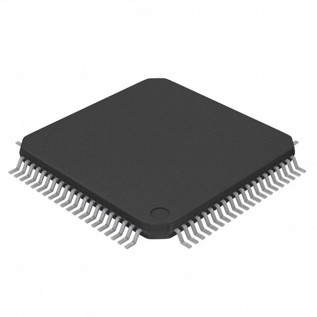
PIC18F87J72 Pin Diagram 1 80-Pin TQFP(1) RE2/LCDBIAS3 RE3/COM0 RE4/COM1 RE5/COM2 RE6/COM3 (2)RE7/CCP2/SEG3 SAVDD RD0/SEG0/CTPLS VDD VSS SVDD ARESET RD1/SEG1 RD2/SEG2 RD3/SEG3 RD4/SEG4 SDIA RD5/SEG5 RD6/SEG6 RD7/SEG7 80 79 78 77 76 75 74 73 72 71 70 69 68 67 66 65 64 63 62 61 CH0+ 1 60 SDOA CH0- 2 59 SCKA RE1/LCDBIAS2 3 58 CSA RE0/LCDBIAS1 4 57 RB0/INT0/SEG30 RG0/LCDBIAS0 5 56 RB1/INT1/SEG8 RG1/TX2/CK2 6 55 RB2/INT2/SEG9/CTED1 RG2/RX2/DT2/VLCAP1 7 54 RB3/INT3/SEG10/CTED2 RG3/VLCAP2 8 53 RB4/KBI0/SEG11 MCLR 9 PIC18F86J72 52 RB5/KBI1/SEG29 RG4/SEG26/RTCC 10 51 RB6/KBI2/PGC VSS 11 PIC18F87J72 50 VSS VDDCORE/VCAP 12 49 OSC2/CLKO/RA6 RF7/AN5/SS/SEG25 13 48 OSC1/CLKI/RA7 RF6/AN11/SEG24/C1INA 14 47 VDD RF5/AN10/CVREF/SEG23/C1INB 15 46 RB7/KBI3/PGD RF4/AN9/SEG22/C2INA 16 45 RC5/SDO/SEG12 RF3/AN8/SEG21/C2INB 17 44 RC4/SDI/SDA/SEG16 RF2/AN7/C1OUT/SEG20 18 43 RC3/SCK/SCL/SEG17 CH1- 19 42 RC2/CCP1/SEG13 CH1+ 20 41 CLKIA 21 22 23 24 25 26 27 28 29 30 31 32 33 34 35 36 37 38 39 40 1/AN6/C2OUT/SEG19 ENVREG AVDD AVSS RA3/AN3/V+REF SAVSS RA2/AN2/V-REF REFIN+/OUT REFIN- RA1/AN1/SEG18 RA0/AN0 VSS RA5/AN4/SEG15 RA4/T0CKI/SEG14 (2)1OSI/CCP2I/SEG32 SVSS RC0/T1OSO/T13CKI RC6/TX1/CK1/SEG27 RC7/RX1/DT1/SEG28 DR F T R 1/ C R Pins are tolerant up to 5.5V Dedicated 24-bit AFE pins Note 1: Pinouts are subject to change. 2: The CCP2 pin placement depends on the setting of the CCP2MX Configuration bit. 2010-2016 Microchip Technology Inc. DS30009979B-page 3
PIC18F87J72 Typical Application Circuit: Single-Phase Power Meter 10 MHz 32 kHz L N MAIN OSC H/W RTCC Up to 33 SEG/4 COM CH0+ 24-Bit Current CH0- Sensor(s)(1) CH1+ AFE with SEG/COM LCD Glass PGA CH1- PIC18F87J72(2) Touch CTMU Keypad Line Voltage 12-Bit A/D Measurement Digital I/O UART1 UART2 SPI/I2C Temperature Sensor Low-Voltage Detect EEPROM RF/PLC Indicator LEDs RS-485 Anti-tamper sensors Note 1: Generic current sense configuration shown. Many circuit configurations using current and/or voltage sensing are possible, including the use of shunts, transformers or Rogowski coils. 2: Power metering, with the measurement of active and reactive power, is done with the power metering firmware application available through Microchip Technology. DS30009979B-page 4 2010-2016 Microchip Technology Inc.
PIC18F87J72 Table of Contents 1.0 Device Overview..........................................................................................................................................................................7 2.0 Guidelines for Getting Started with PIC18FJ Microcontrollers...................................................................................................19 3.0 Oscillator Configurations............................................................................................................................................................23 4.0 Power-Managed Modes.............................................................................................................................................................32 5.0 Reset..........................................................................................................................................................................................39 6.0 Memory Organization.................................................................................................................................................................51 7.0 Flash Program Memory..............................................................................................................................................................73 8.0 8 x 8 Hardware Multiplier............................................................................................................................................................83 9.0 Interrupts....................................................................................................................................................................................85 10.0 I/O Ports...................................................................................................................................................................................101 11.0 Timer0 Module.........................................................................................................................................................................120 12.0 Timer1 Module.........................................................................................................................................................................123 13.0 Timer2 Module.........................................................................................................................................................................129 14.0 Timer3 Module.........................................................................................................................................................................131 15.0 Real-Time Clock and Calendar (RTCC)...................................................................................................................................134 16.0 Capture/Compare/PWM (CCP) Modules.................................................................................................................................151 17.0 Liquid Crystal Display (LCD) Driver Module.............................................................................................................................160 18.0 Master Synchronous Serial Port (MSSP) Module....................................................................................................................187 19.0 Enhanced Universal Synchronous Asynchronous Receiver Transmitter (EUSART)...............................................................231 20.0 Addressable Universal Synchronous Asynchronous Receiver Transmitter (AUSART)...........................................................252 21.0 12-Bit Analog-to-Digital Converter (A/D) Module.....................................................................................................................266 22.0 Dual-Channel, 24-Bit Analog Front End (AFE).........................................................................................................................275 23.0 Comparator Module..................................................................................................................................................................285 24.0 Comparator Voltage Reference Module...................................................................................................................................290 25.0 Charge Time Measurement Unit (CTMU)................................................................................................................................293 26.0 Special Features of the CPU....................................................................................................................................................308 27.0 Instruction Set Summary..........................................................................................................................................................321 28.0 Development Support...............................................................................................................................................................372 29.0 Electrical Characteristics..........................................................................................................................................................376 30.0 Packaging Information..............................................................................................................................................................417 Appendix A: Revision History.............................................................................................................................................................420 Appendix B: Dual-Channel, 24-Bit AFE Reference............................................................................................................................421 The Microchip Website......................................................................................................................................................................451 Customer Change Notification Service..............................................................................................................................................451 Customer Support..............................................................................................................................................................................451 Product Identification System............................................................................................................................................................452 2010-2016 Microchip Technology Inc. DS30009979B-page 5
PIC18F87J72 TO OUR VALUED CUSTOMERS It is our intention to provide our valued customers with the best documentation possible to ensure successful use of your Microchip products. To this end, we will continue to improve our publications to better suit your needs. Our publications will be refined and enhanced as new volumes and updates are introduced. If you have any questions or comments regarding this publication, please contact the Marketing Communications Department via E-mail at docerrors@microchip.com. We welcome your feedback. Most Current Data Sheet To obtain the most up-to-date version of this data sheet, please register at our Worldwide Website at: http://www.microchip.com You can determine the version of a data sheet by examining its literature number found on the bottom outside corner of any page. The last character of the literature number is the version number, (e.g., DS30000000A is version A of document DS30000000). Errata An errata sheet, describing minor operational differences from the data sheet and recommended workarounds, may exist for current devices. As device/documentation issues become known to us, we will publish an errata sheet. The errata will specify the revision of silicon and revision of document to which it applies. To determine if an errata sheet exists for a particular device, please check with one of the following: • Microchip’s Worldwide Website; http://www.microchip.com • Your local Microchip sales office (see last page) When contacting a sales office, please specify which device, revision of silicon and data sheet (include literature number) you are using. Customer Notification System Register on our website at www.microchip.com to receive the most current information on all of our products. DS30009979B-page 6 2010-2016 Microchip Technology Inc.
PIC18F87J72 1.0 DEVICE OVERVIEW The internal oscillator block provides a stable reference source that gives the family additional features for This document contains device-specific information for robust operation: the following devices: • Fail-Safe Clock Monitor: This option constantly • PIC18F86J72 monitors the main clock source against a reference • PIC18F87J72 signal provided by the internal oscillator. If a clock This family combines the traditional advantages of all failure occurs, the controller is switched to the PIC18 microcontrollers – namely, high computational internal oscillator, allowing for continued low-speed performance and a rich feature set – with a versatile operation or a safe application shutdown. on-chip LCD driver and a high-performance, • Two-Speed Start-up: This option allows the high-accuracy analog front end. These features make internal oscillator to serve as the clock source the PIC18F87J72 family a logical choice for many from Power-on Reset, or wake-up from Sleep high-performance power and metering applications mode, until the primary clock source is available. where price is a primary consideration. 1.1.3 MEMORY OPTIONS 1.1 Core Features The PIC18F87J72 family provides ample room for application code with 128Kbytes of code space. The 1.1.1 LOW-POWER MODES Flash cells for program memory are rated to last up to 10,000 erase/write cycles. Data retention without All of the devices in the PIC18F87J72 family incorporate refresh is conservatively estimated to be greater than a range of features that can significantly reduce power 20 years. consumption during operation. Key items include: The Flash program memory is readable and writable. • Alternate Run Modes: By clocking the controller During normal operation, the PIC18F87J72 family also from the Timer1 source or the internal RC provides plenty of room for dynamic application data oscillator, power consumption during code with up to 3,923bytes of data RAM. execution can be reduced by as much as 90%. • Multiple Idle Modes: The controller can also run 1.1.4 EXTENDED INSTRUCTION SET with its CPU core disabled but the peripherals still The PIC18F87J72 family implements the optional active. In these states, power consumption can be extension to the PIC18 instruction set, adding 8 new reduced even further, to as little as 4% of normal instructions and an Indexed Addressing mode. operation requirements. Enabled as a device configuration option, the extension • On-the-Fly Mode Switching: The power-managed has been specifically designed to optimize re-entrant modes are invoked by user code during operation, application code originally developed in high-level allowing the user to incorporate power-saving ideas languages, such as ‘C’. into their application’s software design. 1.1.5 EASY MIGRATION 1.1.2 OSCILLATOR OPTIONS AND Regardless of the memory size, all devices share the FEATURES same rich set of peripherals, allowing for a smooth All of the devices in the PIC18F87J72 family offer six migration path as applications grow and evolve. different oscillator options, allowing users a range of The consistent pinout scheme used throughout the choices in developing application hardware. These entire family also aids in migrating to the next larger include: device. • Two Crystal modes using crystals or ceramic The PIC18F87J72 family is also largely pin compatible resonators. with other PIC18 families, such as the PIC18F8720 and • Two External Clock modes offering the option of a PIC18F8722, the PIC18F85J11, and the PIC18F8490 divide-by-4 clock output. and PIC18F85J90 families of microcontrollers with • A Phase Lock Loop (PLL) frequency multiplier, LCD drivers. This allows a new dimension to the available to the external oscillator modes which evolution of applications, allowing developers to select allows clock speeds of up to 40MHz. PLL can different price points within Microchip’s PIC18 portfolio, also be used with the internal oscillator. while maintaining a similar feature set. • An internal oscillator block which provides an 8MHz clock (±2% accuracy) and an INTRC source (approximately 31kHz, stable over temperature and VDD), as well as a range of six user-selectable clock frequencies, between 125kHz to 4MHz, for a total of eight clock frequencies. This option frees the two oscillator pins for use as additional general purpose I/O. 2010-2016 Microchip Technology Inc. DS30009979B-page 7
PIC18F86J72 1.2 Analog Features 1.4 Other Special Features • Dual-Channel, 24-Bit ADC Front End (AFE): • Communications: The PIC18F87J72 family This module contains two synchronous sampling, incorporates a range of serial communication Analog-to-Digital (A/D) Converters, plus sup- peripherals, including an Addressable USART, a porting Programmable Gain Amplifiers (PGAs) separate Enhanced USART that supports and an internal voltage reference, to perform LIN/J2602 specification 1.2, and one Master SSP high-accuracy and low noise analog conversions. module capable of both SPI and I2C (Master and The AFE is controlled, and its data read, through Slave) modes of operation. a dedicated, high-speed (20 MHz) SPI interface. • CCP Modules: All devices in the family incorporate • 12-Bit A/D Converter: In addition to the AFE, two Capture/Compare/PWM (CCP) modules. Up to PIC18F87J72 family devices also include a stan- four different time bases may be used to perform dard SAR A/D Converter with 12 independent several different operations at once. analog inputs. The module incorporates program- • Extended Watchdog Timer (WDT): This mable acquisition time, allowing for a channel to enhanced version incorporates a 16-bit prescaler, be selected and a conversion to be initiated allowing an extended time-out range that is stable without waiting for a sampling period and thus, across operating voltage and temperature. See reducing code overhead. Section29.0 “Electrical Characteristics” for • Charge Time Measurement Unit (CTMU): The time-out periods. CTMU is a flexible analog module that provides • Real Time Clock and Calendar Module (RTCC): accurate differential time measurement between The RTCC module is intended for applications pulse sources, as well as asynchronous pulse requiring that accurate time be maintained for generation. extended periods of time with minimum to no Together with other on-chip analog modules, the intervention from the CPU. CTMU can precisely measure time, measure The module is a 100-year clock and calendar with capacitance or relative changes in capacitance, or automatic leap year detection. The range of the generate output pulses that are independent of clock is from 00:00:00 (midnight) on January 1, the system clock. 2000 to 23:59:59 on December 31, 2099. 1.3 LCD Driver The on-chip LCD driver includes many features that make the integration of displays in low-power applications easier. These include an integrated volt- age regulator with charge pump that allows contrast control in software and display operation above device VDD. DS30009979B-page 8 2010-2016 Microchip Technology Inc.
PIC18F87J72 1.5 Details on Individual Family The devices are differentiated in that PIC18F86J72 Members devices have a Flash program memory of 64Kbytes and PIC18F87J72 devices memory is 128Kbytes Devices in the PIC18F87J72 family are available in All other features for the devices are identical. These 80-pin packages. Block diagrams for the two groups are summarized in Table1-1. are shown in Figure1-1. The pinouts for all devices are listed in Table1-2. TABLE 1-1: DEVICE FEATURES FOR THE PIC18F8XJ72 (80-PIN DEVICES) Features PIC18F86J72 PIC18F87J72 Operating Frequency DC – 48 MHz Program Memory (Bytes) 64K 128K Program Memory (Instructions) 32,768 65,536 Data Memory (Bytes) 3,923 3,923 Interrupt Sources 29 I/O Ports Ports A, B, C, D, E, F, G LCD Driver (available pixels to drive) 132 (33 SEGs x 4 COMs) Timers 4 Comparators 2 CTMU Yes RTCC Yes Capture/Compare/PWM Modules 2 Serial Communications MSSP, Addressable USART, Enhanced USART 12-Bit Analog-to-Digital Module 12 Input Channels Dual-Channel 24-Bit Analog Front End Yes Resets (and Delays) POR, BOR, RESET Instruction, Stack Full, Stack Underflow, MCLR, WDT (PWRT, OST) Instruction Set 75 Instructions, 83 with Extended Instruction Set Enabled Packages 80-Pin TQFP 2010-2016 Microchip Technology Inc. DS30009979B-page 9
PIC18F86J72 FIGURE 1-1: PIC18F8XJ72 (80-PIN) BLOCK DIAGRAM Data Bus<8> Table Pointer<21> PORTA Data Latch inc/dec logic 8 8 RA0:RA7(1,2) Data Memory (2.0, 3.9 21 PCLAT U PCLATH Kbytes) 20 Address Latch PCU PCH PCL PORTB Program Counter 12 RB0:RB7(1) Data Address<12> 31-Level Stack Address Latch 4 12 4 BSR Access Program Memory STKPTR FSR0 Bank PORTC (96Kbytes) FSR1 Data Latch FSR2 12 RC0:RC7(1) inc/dec 8 logic Table Latch PORTD ROM Latch Address RD0:RD7(1) Instruction Bus <16> Decode IR PORTE 8 RE0:RE1, Instruction State Machine RE3:RE7(1) Decode and Control Signals Control PRODH PRODL 8 x 8 Multiply PORTF OSC2/CLKO GeTnimeriantgion Power-up 3 8 RF1:RF7(1) OSC1/CLKI Timer BITOP W OIsNcTilRlaCtor StaOrts-cuiplla Ttoimrer 8 8 8 8 MHz Oscillator Power-on 8 8 PORTG Reset Precision ALU<8> RG0:RG4(1) Band Gap Watchdog Reference Timer 8 ENVREG BOR and Voltage LVD(3) Regulator SDIA CHn+SDOA VDDCORE/VCAP VDD,VSS MCLR CHn- CSA CLKIADR ADC Timer0 Timer1 Timer2 Timer3 CTMU Comparators 12-Bit Dual-Channel AFE CCP1 CCP2 AUSART EUSART RTCC MSSP LCD SVDD SAVDD ARESET Driver SVSS SAVSS Note 1: See Table1-2 for I/O port pin descriptions. 2: RA6 and RA7 are only available as digital I/O in select oscillator modes. See Section3.0 “Oscillator Configurations” for more information 3: Brown-out Reset and Low-Voltage Detect functions are provided when the on-board voltage regulator is enabled. DS30009979B-page 10 2010-2016 Microchip Technology Inc.
PIC18F87J72 TABLE 1-2: PIC18F8XJ72 PINOUT I/O DESCRIPTIONS Pin Number Pin Buffer Pin Name Description Type Type TQFP MCLR 9 I ST Master Clear (input) or programming voltage (input). This pin is an active-low Reset to the device. OSC1/CLKI/RA7 48 Oscillator crystal or external clock input. OSC1 I CMOS Oscillator crystal input. CLKI I CMOS External clock source input. Always associated with pin function, OSC1. (See related OSC1/CLKI, OSC2/CLKO pins.) RA7 I/O TTL General purpose I/O pin. OSC2/CLKO/RA6 49 Oscillator crystal or clock output. OSC2 O — Oscillator crystal output. Connects to crystal or resonator in Crystal Oscillator mode. CLKO O — In EC modes, OSC2 pin outputs CLKO, which has 1/4 the frequency of OSC1 and denotes the instruction cycle rate. RA6 I/O TTL General purpose I/O pin. PORTA is a bidirectional I/O port. RA0/AN0 31 RA0 I/O TTL Digital I/O. AN0 I Analog Analog Input 0. RA1/AN1/SEG18 30 RA1 I/O TTL Digital I/O. AN1 I Analog Analog Input 1. SEG18 O Analog SEG18 output for LCD. RA2/AN2/VREF- 27 RA2 I/O TTL Digital I/O. AN2 I Analog Analog Input 2. VREF- I Analog A/D reference voltage (low) input. RA3/AN3/VREF+ 25 RA3 I/O TTL Digital I/O. AN3 I Analog Analog Input 3. VREF+ I Analog A/D reference voltage (high) input. RA4/T0CKI/SEG14 34 RA4 I/O ST Digital I/O. T0CKI I ST Timer0 external clock input. SEG14 O Analog SEG14 output for LCD. RA5/AN4/SEG15 33 RA5 I/O TTL Digital I/O. AN4 I Analog Analog Input 4. SEG15 O Analog SEG15 output for LCD. RA6 See the OSC2/CLKO/RA6 pin. RA7 See the OSC1/CLKI/RA7 pin. Legend: TTL = TTL compatible input CMOS = CMOS compatible input or output ST = Schmitt Trigger input with CMOS levels Analog = Analog input I2C = I2C/SMBus compatible input OD = Open-Drain (no P diode to VDD) I = Input O = Output P = Power Note 1: Default assignment for CCP2 when the CCP2MX Configuration bit is set. 2: Alternate assignment for CCP2 when the CCP2MX Configuration bit is cleared. 2010-2016 Microchip Technology Inc. DS30009979B-page 11
PIC18F86J72 TABLE 1-2: PIC18F8XJ72 PINOUT I/O DESCRIPTIONS (CONTINUED) Pin Number Pin Buffer Pin Name Description Type Type TQFP PORTB is a bidirectional I/O port. PORTB can be software programmed for internal weak pull-ups on all inputs. RB0/INT0/SEG30 57 RB0 I/O TTL Digital I/O. INT0 I ST External Interrupt 0. SEG30 O Analog SEG30 output for LCD. RB1/INT1/SEG8 56 RB1 I/O TTL Digital I/O. INT1 I ST External Interrupt 1. SEG8 O Analog SEG8 output for LCD. RB2/INT2/SEG9/ 55 CTED1 RB2 I/O TTL Digital I/O. INT2 I ST External Interrupt 2. CTED1 I ST CTMU Edge 1 input. SEG9 O Analog SEG9 output for LCD. RB3/INT3/SEG10/ 54 CTED2 RB3 I/O TTL Digital I/O. INT3 I ST External Interrupt 3. SEG10 O Analog SEG10 output for LCD. CTED2 I ST CTMU Edge 2 input. RB4/KBI0/SEG11 53 RB4 I/O TTL Digital I/O. KBI0 I TTL Interrupt-on-change pin. SEG11 O Analog SEG11 output for LCD. RB5/KBI1/SEG29 52 RB5 I/O TTL Digital I/O. KBI1 I TTL Interrupt-on-change pin. SEG29 O Analog SEG29 output for LCD. RB6/KBI2/PGC 51 RB6 I/O TTL Digital I/O. KBI2 I TTL Interrupt-on-change pin. PGC I/O ST In-Circuit Debugger and ICSP™ programming clock pin. RB7/KBI3/PGD 46 RB7 I/O TTL Digital I/O. KBI3 I TTL Interrupt-on-change pin. PGD I/O ST In-Circuit Debugger and ICSP programming data pin. Legend: TTL = TTL compatible input CMOS = CMOS compatible input or output ST = Schmitt Trigger input with CMOS levels Analog = Analog input I2C = I2C/SMBus compatible input OD = Open-Drain (no P diode to VDD) I = Input O = Output P = Power Note 1: Default assignment for CCP2 when the CCP2MX Configuration bit is set. 2: Alternate assignment for CCP2 when the CCP2MX Configuration bit is cleared. DS30009979B-page 12 2010-2016 Microchip Technology Inc.
PIC18F87J72 TABLE 1-2: PIC18F8XJ72 PINOUT I/O DESCRIPTIONS (CONTINUED) Pin Number Pin Buffer Pin Name Description Type Type TQFP PORTC is a bidirectional I/O port. RC0/T1OSO/T13CKI 37 RC0 I/O ST Digital I/O. T1OSO O — Timer1 oscillator output. T13CKI I ST Timer1/Timer3 external clock input. RC1/T1OSI/CCP2/ 35 SEG32 RC1 I/O ST Digital I/O. T1OSI I CMOS Timer1 oscillator input. CCP2(1) I/O ST Capture 2 input/Compare 2 output/PWM2 output. SEG32 O Analog SEG32 output for LCD. RC2/CCP1/SEG13 42 RC2 I/O ST Digital I/O. CCP1 I/O ST Capture 1 input/Compare 1 output/PWM1 output. SEG13 O Analog SEG13 output for LCD. RC3/SCK/SCL/SEG1 43 7 I/O ST Digital I/O. RC3 I/O ST Synchronous serial clock input/output for SPI mode. SCK I/O I2C Synchronous serial clock input/output for I2C mode. SCL O Analog SEG17 output for LCD. SEG17 RC4/SDI/SDA/SEG16 44 RC4 I/O ST Digital I/O. SDI I ST SPI data in. SDA I/O I2C I2C data I/O. SEG16 O Analog SEG16 output for LCD. RC5/SDO/SEG12 45 RC5 I/O ST Digital I/O. SDO O — SPI data out. SEG12 O Analog SEG12 output for LCD. RC6/TX1/CK1/SEG27 38 RC6 I/O ST Digital I/O. TX1 O — EUSART asynchronous transmit. CK1 I/O ST EUSART synchronous clock (see related RX1/DT1). SEG27 O Analog SEG27 output for LCD. RC7/RX1/DT1/SEG28 39 RC7 I/O ST Digital I/O. RX1 I ST EUSART asynchronous receive. DT1 I/O ST EUSART synchronous data (see related TX1/CK1). SEG28 O Analog SEG28 output for LCD. Legend: TTL = TTL compatible input CMOS = CMOS compatible input or output ST = Schmitt Trigger input with CMOS levels Analog = Analog input I2C = I2C/SMBus compatible input OD = Open-Drain (no P diode to VDD) I = Input O = Output P = Power Note 1: Default assignment for CCP2 when the CCP2MX Configuration bit is set. 2: Alternate assignment for CCP2 when the CCP2MX Configuration bit is cleared. 2010-2016 Microchip Technology Inc. DS30009979B-page 13
PIC18F86J72 TABLE 1-2: PIC18F8XJ72 PINOUT I/O DESCRIPTIONS (CONTINUED) Pin Number Pin Buffer Pin Name Description Type Type TQFP PORTD is a bidirectional I/O port. RD0/SEG0/CTPLS 73 RD0 I/O ST Digital I/O. SEG0 O Analog SEG0 output for LCD. CTPLS O — CTMU pulse generator output. RD1/SEG1 68 RD1 I/O ST Digital I/O. SEG1 O Analog SEG1 output for LCD. RD2/SEG2 67 RD2 I/O ST Digital I/O. SEG2 O Analog SEG2 output for LCD. RD3/SEG3 66 RD3 I/O ST Digital I/O. SEG3 O Analog SEG3 output for LCD. RD4/SEG4 65 RD4 I/O ST Digital I/O. SEG4 O Analog SEG4 output for LCD. RD5/SEG5 63 RD5 I/O ST Digital I/O. SEG5 O Analog SEG5 output for LCD. RD6/SEG6 62 RD6 I/O ST Digital I/O. SEG6 O Analog SEG6 output for LCD. RD7/SEG7 61 RD7 I/O ST Digital I/O. SEG7 O Analog SEG7 output for LCD. Legend: TTL = TTL compatible input CMOS = CMOS compatible input or output ST = Schmitt Trigger input with CMOS levels Analog = Analog input I2C = I2C/SMBus compatible input OD = Open-Drain (no P diode to VDD) I = Input O = Output P = Power Note 1: Default assignment for CCP2 when the CCP2MX Configuration bit is set. 2: Alternate assignment for CCP2 when the CCP2MX Configuration bit is cleared. DS30009979B-page 14 2010-2016 Microchip Technology Inc.
PIC18F87J72 TABLE 1-2: PIC18F8XJ72 PINOUT I/O DESCRIPTIONS (CONTINUED) Pin Number Pin Buffer Pin Name Description Type Type TQFP PORTE is a bidirectional I/O port. RE0/LCDBIAS1 4 RE0 I/O ST Digital I/O. LCDBIAS1 I Analog BIAS1 input for LCD. RE1/LCDBIAS2 3 RE1 I/O ST Digital I/O. LCDBIAS2 I Analog BIAS2 input for LCD. RE2/LCDBIAS3 80 RE2 I/O ST Digital I/O. LCDBIAS3 I Analog BIAS3 input for LCD. RE3/COM0 79 RE3 I/O ST Digital I/O. COM0 O Analog COM0 output for LCD. RE4/COM1 78 RE4 I/O ST Digital I/O. COM1 O Analog COM1 output for LCD. RE5/COM2 77 RE5 I/O ST Digital I/O. COM2 O Analog COM2 output for LCD. RE6/COM3 76 RE6 I/O ST Digital I/O. COM3 O Analog COM3 output for LCD. RE7/CCP2/SEG31 75 RE7 I/O ST Digital I/O. CCP2(2) I/O ST Capture 2 input/Compare 2 output/PWM2 output. SEG31 O Analog SEG31 output for LCD. Legend: TTL = TTL compatible input CMOS = CMOS compatible input or output ST = Schmitt Trigger input with CMOS levels Analog = Analog input I2C = I2C/SMBus compatible input OD = Open-Drain (no P diode to VDD) I = Input O = Output P = Power Note 1: Default assignment for CCP2 when the CCP2MX Configuration bit is set. 2: Alternate assignment for CCP2 when the CCP2MX Configuration bit is cleared. 2010-2016 Microchip Technology Inc. DS30009979B-page 15
PIC18F86J72 TABLE 1-2: PIC18F8XJ72 PINOUT I/O DESCRIPTIONS (CONTINUED) Pin Number Pin Buffer Pin Name Description Type Type TQFP PORTF is a bidirectional I/O port. RF1/AN6/C2OUT/ 21 SEG19 RF1 I/O ST Digital I/O. AN6 I Analog Analog Input 6. C2OUT O — Comparator 2 output. SEG19 O Analog SEG19 output for LCD. RF2/AN7/C1OUT/ 18 SEG20 RF2 I/O ST Digital I/O. AN7 I Analog Analog Input 7. C1OUT O — Comparator 1 output. SEG20 O Analog SEG20 output for LCD. RF3/AN8/SEG21/ 17 C2INB RF3 I/O ST Digital I/O. AN8 I Analog Analog Input 8. SEG21 O Analog SEG21 output for LCD. C2INB I Analog Comparator 2 Input B. RF4/AN9/SEG22/ 16 C2INA RF4 I/O ST Digital I/O. AN9 I Analog Analog Input 9. SEG22 O Analog SEG22 output for LCD C2INA I Analog Comparator 2 Input A. RF5/AN10/CVREF/ 15 SEG23/C1INB RF5 I/O ST Digital I/O. AN10 I Analog Analog Input 10. CVREF O Analog Comparator reference voltage output. SEG23 O Analog SEG23 output for LCD. C1INB I Analog Comparator 1 Input B. RF6/AN11/SEG24/ 14 C1INA RF6 I/O ST Digital I/O. AN11 I Analog Analog Input 11. SEG24 O Analog SEG24 output for LCD C1INA I Analog Comparator 1 Input A. RF7/AN5/SS/SEG25 13 RF7 I/O ST Digital I/O. AN5 O Analog Analog Input 5. SS I TTL SPI slave select input. SEG25 O Analog SEG25 output for LCD. Legend: TTL = TTL compatible input CMOS = CMOS compatible input or output ST = Schmitt Trigger input with CMOS levels Analog = Analog input I2C = I2C/SMBus compatible input OD = Open-Drain (no P diode to VDD) I = Input O = Output P = Power Note 1: Default assignment for CCP2 when the CCP2MX Configuration bit is set. 2: Alternate assignment for CCP2 when the CCP2MX Configuration bit is cleared. DS30009979B-page 16 2010-2016 Microchip Technology Inc.
PIC18F87J72 TABLE 1-2: PIC18F8XJ72 PINOUT I/O DESCRIPTIONS (CONTINUED) Pin Number Pin Buffer Pin Name Description Type Type TQFP PORTG is a bidirectional I/O port. RG0/LCDBIAS0 5 RG0 I/O ST Digital I/O. LCDBIAS0 I Analog BIAS0 input for LCD. RG1/TX2/CK2 6 RG1 I/O ST Digital I/O. TX2 O — AUSART asynchronous transmit. CK2 I/O ST AUSART synchronous clock (see related RX2/DT2). RG2/RX2/DT2/VLCAP 7 1 I/O ST Digital I/O. RG2 I ST AUSART asynchronous receive. RX2 I/O ST AUSART synchronous data (see related TX2/CK2). DT2 I Analog LCD charge pump capacitor input. VLCAP1 RG3/VLCAP2 8 RG3 I/O ST Digital I/O. VLCAP2 I Analog LCD charge pump capacitor input. RG4/SEG26/RTCC 10 RG4 I/O ST Digital I/O. SEG26 O Analog SEG26 output for LCD. RTCC O — RTCC output. VSS 11,32,50, 71 P — Ground reference for logic and I/O pins. VDD 47, 72 P — Positive supply for logic and I/O pins. AVSS 24 P — Ground reference for analog modules. AVDD 23 P — Positive supply for analog modules. ENVREG 22 I ST Enable for on-chip voltage regulator. VDDCORE/VCAP 12 Core logic power or external filter capacitor connection. VDDCORE P — Positive supply for microcontroller core logic (regulator disabled). VCAP P — External filter capacitor connection (regulator enabled). Legend: TTL = TTL compatible input CMOS = CMOS compatible input or output ST = Schmitt Trigger input with CMOS levels Analog = Analog input I2C = I2C/SMBus compatible input OD = Open-Drain (no P diode to VDD) I = Input O = Output P = Power Note 1: Default assignment for CCP2 when the CCP2MX Configuration bit is set. 2: Alternate assignment for CCP2 when the CCP2MX Configuration bit is cleared. 2010-2016 Microchip Technology Inc. DS30009979B-page 17
PIC18F86J72 TABLE 1-2: PIC18F8XJ72 PINOUT I/O DESCRIPTIONS (CONTINUED) Pin Number Pin Buffer Pin Name Description Type Type TQFP RESET 69 I ST AFE Master Reset logic input pin. SVDD 70 P — AFE digital power supply pin. SAVDD 74 P — AFE analog power supply reference pin. CH0+ 1 I Analog Channel 0 non-inverting analog input pin. CH0- 2 I Analog Channel 0 inverting analog input pin. CH1- 19 I Analog Channel 1 inverting analog input pin. CH1+ 20 I Analog Channel 1 Non-Inverting Analog Input Pin SAVSS 26 P — AFE analog ground pin (return path for analog circuitry). REFIN+/OUT 28 REFIN+ I Analog AFE non-inverting voltage reference input. REFOUT O Analog Internal reference output pin. REFIN- 29 I Analog Inverting voltage reference input pin. SVSS 36 P — AFE digital ground pin (return path for digital circuitry). DR 40 — AFE data ready signal output pin. CLKIA 41 I CMOS AFE oscillator crystal connection pin or external clock input pin. CSA 58 I TTL AFE serial interface chip select pin. SCKA 59 I TTL AFE serial interface clock pin. SDOA 60 O TTL AFE serial interface data output pin. SDIA 64 I TTL AFE serial interface data input pin. Legend: TTL = TTL compatible input CMOS = CMOS compatible input or output ST = Schmitt Trigger input with CMOS levels Analog = Analog input I2C = I2C/SMBus compatible input OD = Open-Drain (no P diode to VDD) I = Input O = Output P = Power Note 1: Default assignment for CCP2 when the CCP2MX Configuration bit is set. 2: Alternate assignment for CCP2 when the CCP2MX Configuration bit is cleared. DS30009979B-page 18 2010-2016 Microchip Technology Inc.
PIC18F87J72 2.0 GUIDELINES FOR GETTING FIGURE 2-1: RECOMMENDED MINIMUM STARTED WITH PIC18FJ CONNECTIONS MICROCONTROLLERS C2(2) 2.1 Basic Connection Requirements VDD Getting started with the PIC18F87J72 family family of R1 DD SS (1) (1) 8-bit microcontrollers requires attention to a minimal V V R2 set of device pin connections before proceeding with MCLR ENVREG development. VCAP/VDDCORE C1 The following pins must always be connected: C7 PIC18FXXJXX • All VDD and VSS pins (see Section2.2 “Power Supply Pins”) VSS VDD C6(2) C3(2) • All AVDD and AVSS pins, regardless of whether or not the analog device features are used VDD D S VSS D S D S (see Section2.2 “Power Supply Pins”) V V D S A A V V • MCLR pin (see Section2.3 “Master Clear (MCLR) Pin”) C5(2) C4(2) • ENVREG (if implemented) and VCAP/VDDCORE pins (see Section2.4 “Voltage Regulator Pins (ENVREG and VCAP/VDDCORE)”) Key (all values are recommendations): These pins must also be connected if they are being C1 through C6: 0.1 F, 20V ceramic used in the end application: C7: 10 F, 6.3V or greater, tantalum or ceramic • PGC/PGD pins used for In-Circuit Serial R1: 10 kΩ Programming™ (ICSP™) and debugging purposes R2: 100Ω to 470Ω (see Section2.5 “ICSP Pins”) Note 1: See Section2.4 “Voltage Regulator Pins • OSCI and OSCO pins when an external oscillator (ENVREG and VCAP/VDDCORE)” for source is used explanation of ENVREG pin connections. (see Section2.6 “External Oscillator Pins”) 2: The example shown is for a PIC18F device Additionally, the following pins may be required: with five VDD/VSS and AVDD/AVSS pairs. Other devices may have more or less pairs; • VREF+/VREF- pins are used when external voltage adjust the number of decoupling capacitors reference for analog modules is implemented appropriately. Note: The AVDD and AVSS pins must always be connected, regardless of whether any of the analog modules are being used. The minimum mandatory connections are shown in Figure2-1. 2010-2016 Microchip Technology Inc. DS30009979B-page 19
PIC18F87J72 2.2 Power Supply Pins 2.3 Master Clear (MCLR) Pin 2.2.1 DECOUPLING CAPACITORS The MCLR pin provides two specific device functions: Device Reset, and Device Programming The use of decoupling capacitors on every pair of and Debugging. If programming and debugging are power supply pins, such as VDD, VSS, AVDD and not required in the end application, a direct AVSS, is required. connection to VDD may be all that is required. The Consider the following criteria when using decoupling addition of other components, to help increase the capacitors: application’s resistance to spurious Resets from voltage sags, may be beneficial. A typical • Value and type of capacitor: A 0.1 F (100 nF), configuration is shown in Figure2-1. Other circuit 10-20V capacitor is recommended. The capacitor designs may be implemented, depending on the should be a low-ESR device, with a resonance application’s requirements. frequency in the range of 200MHz and higher. Ceramic capacitors are recommended. During programming and debugging, the resistance • Placement on the printed circuit board: The and capacitance that can be added to the pin must decoupling capacitors should be placed as close be considered. Device programmers and debuggers to the pins as possible. It is recommended to drive the MCLR pin. Consequently, specific voltage place the capacitors on the same side of the levels (VIH and VIL) and fast signal transitions must not be adversely affected. Therefore, specific values board as the device. If space is constricted, the of R1 and C1 will need to be adjusted based on the capacitor can be placed on another layer on the application and PCB requirements. For example, it is PCB using a via; however, ensure that the trace recommended that the capacitor, C1, be isolated length from the pin to the capacitor is no greater from the MCLR pin during programming and than 0.25inch (6mm). debugging operations by using a jumper (Figure2-2). • Handling high-frequency noise: If the board is The jumper is replaced for normal run-time experiencing high-frequency noise (upward of operations. tens of MHz), add a second ceramic type capaci- tor in parallel to the above described decoupling Any components associated with the MCLR pin capacitor. The value of the second capacitor can should be placed within 0.25 inch (6mm) of the pin. be in the range of 0.01F to 0.001F. Place this second capacitor next to each primary decoupling FIGURE 2-2: EXAMPLE OF MCLR PIN capacitor. In high-speed circuit designs, consider CONNECTIONS implementing a decade pair of capacitances as close to the power and ground pins as possible VDD (e.g., 0.1F in parallel with 0.001F). • Maximizing performance: On the board layout R1 from the power supply circuit, run the power and R2 return traces to the decoupling capacitors first, MCLR and then to the device pins. This ensures that the JP PIC18FXXJXX decoupling capacitors are first in the power chain. Equally important is to keep the trace length C1 between the capacitor and the power pins to a minimum, thereby reducing PCB trace inductance. Note 1: R1 10k is recommended. A suggested 2.2.2 TANK CAPACITORS starting value is 10k. Ensure that the On boards with power traces running longer than MCLR pin VIH and VIL specifications are met. sixinches in length, it is suggested to use a tank capac- 2: R2470 will limit any current flowing into itor for integrated circuits, including microcontrollers, to MCLR from the external capacitor, C, in the supply a local power source. The value of the tank event of MCLR pin breakdown, due to Electrostatic Discharge (ESD) or Electrical capacitor should be determined based on the trace Overstress (EOS). Ensure that the MCLR pin resistance that connects the power supply source to VIH and VIL specifications are met. the device, and the maximum current drawn by the device in the application. In other words, select the tank capacitor so that it meets the acceptable voltage sag at the device. Typical values range from 4.7F to 47F. DS30009979B-page 20 2010-2016 Microchip Technology Inc.
PIC18F87J72 2.4 Voltage Regulator Pins (ENVREG 2.5 ICSP Pins and VCAP/VDDCORE) The PGC and PGD pins are used for In-Circuit Serial The on-chip voltage regulator enable pin, ENVREG, Programming™ (ICSP™) and debugging purposes. It must always be connected directly to either a supply is recommended to keep the trace length between the voltage or to ground. Tying ENVREG to VDD enables ICSP connector and the ICSP pins on the device as the regulator, while tying it to ground disables the short as possible. If the ICSP connector is expected to regulator. Refer to Section26.3 “On-Chip Voltage experience an ESD event, a series resistor is recom- Regulator” for details on connecting and using the mended, with the value in the range of a few tens of on-chip regulator. ohms, not to exceed 100Ω. When the regulator is enabled, a low-ESR (<5Ω) Pull-up resistors, series diodes, and capacitors on the capacitor is required on the VCAP/VDDCORE pin to PGC and PGD pins are not recommended as they will stabilize the voltage regulator output voltage. The interfere with the programmer/debugger communica- VCAP/VDDCORE pin must not be connected to VDD and tions to the device. If such discrete components are an must use a capacitor of 10 F connected to ground. The application requirement, they should be removed from type can be ceramic or tantalum. A suitable example is the circuit during programming and debugging. Alter- the Murata GRM21BF50J106ZE01 (10 F, 6.3V) or natively, refer to the AC/DC characteristics and timing equivalent. Designers may use Figure2-3 to evaluate requirements information in the respective device ESR equivalence of candidate devices. Flash programming specification for information on capacitive loading limits, and pin input voltage high It is recommended that the trace length not exceed (VIH) and input low (VIL) requirements. 0.25inch (6mm). Refer to Section29.0 “Electrical Characteristics” for additional information. For device emulation, ensure that the “Communication Channel Select” (i.e., PGCx/PGDx pins) programmed When the regulator is disabled, the VCAP/VDDCORE pin into the device matches the physical connections for must be tied to a voltage supply at the VDDCORE level. the ICSP to the Microchip debugger/emulator tool. Refer to Section29.0 “Electrical Characteristics” for information on VDD and VDDCORE. For more information on available Microchip development tools connection requirements, refer to Note that the “LF” versions of some low pin count Section28.0 “Development Support”. PIC18FJ parts (e.g., the PIC18LF45J10) do not have the ENVREG pin. These devices are provided with the voltage regulator permanently disabled; they must always be provided with a supply voltage on the VDDCORE pin. FIGURE 2-3: FREQUENCY vs. ESR PERFORMANCE FOR SUGGESTED VCAP 10 1 ) R ( 0.1 S E 0.01 0.001 0.01 0.1 1 10 100 1000 10,000 Frequency (MHz) Note: Data for Murata GRM21BF50J106ZE01 shown. Measurements at 25°C, 0V DC bias. 2010-2016 Microchip Technology Inc. DS30009979B-page 21
PIC18F87J72 2.6 External Oscillator Pins FIGURE 2-4: SUGGESTED PLACEMENT OF THE OSCILLATOR Many microcontrollers have options for at least two CIRCUIT oscillators: a high-frequency primary oscillator and a low-frequency secondary oscillator (refer to Single-Sided and In-Line Layouts: Section3.0 “Oscillator Configurations” for details). Copper Pour Primary Oscillator The oscillator circuit should be placed on the same (tied to ground) Crystal side of the board as the device. Place the oscillator DEVICE PINS circuit close to the respective oscillator pins with no more than 0.5inch (12mm) between the circuit components and the pins. The load capacitors should be placed next to the oscillator itself, on the same side Primary OSC1 Oscillator of the board. C1 ` OSC2 Use a grounded copper pour around the oscillator cir- cuit to isolate it from surrounding circuits. The C2 GND grounded copper pour should be routed directly to the ` MCU ground. Do not run any signal traces or power T1OSO traces inside the ground pour. Also, if using a two-sided board, avoid any traces on the other side of the board T1OS I Timer1 Oscillator where the crystal is placed. Crystal ` Layout suggestions are shown in Figure 2-4. In-line packages may be handled with a single-sided layout that completely encompasses the oscillator pins. With T1 Oscillator: C1 T1 Oscillator: C2 fine-pitch packages, it is not always possible to com- pletely surround the pins and components. A suitable solution is to tie the broken guard sections to a mirrored Fine-Pitch (Dual-Sided) Layouts: ground layer. In all cases, the guard trace(s) must be returned to ground. Top Layer Copper Pour (tied to ground) In planning the application’s routing and I/O assign- ments, ensure that adjacent port pins and other signals Bottom Layer in close proximity to the oscillator are benign (i.e., free Copper Pour of high frequencies, short rise and fall times, and other (tied to ground) similar noise). OSCO For additional information and design guidance on oscillator circuits, please refer to these Microchip C2 Application Notes, available at the corporate website Oscillator (www.microchip.com): GND Crystal • AN826, “Crystal Oscillator Basics and Crystal C1 Selection for rfPIC™ and PICmicro® Devices” • AN849, “Basic PICmicro® Oscillator Design” OSCI • AN943, “Practical PICmicro® Oscillator Analysis and Design” • AN949, “Making Your Oscillator Work” 2.7 Unused I/Os DEVICE PINS Unused I/O pins should be configured as outputs and driven to a logic low state. Alternatively, connect a 1kΩ to 10kΩ resistor to VSS on unused pins and drive the output to logic low. DS30009979B-page 22 2010-2016 Microchip Technology Inc.
PIC18F87J72 3.0 OSCILLATOR All of these modes are selected by the user by CONFIGURATIONS programming the FOSC<2:0> Configuration bits. In addition, PIC18F87J72 family devices can switch 3.1 Oscillator Types between different clock sources, either under software control or automatically under certain conditions. This The PIC18F87J72 family of devices can be operated in allows for additional power savings by managing eight different oscillator modes: device clock speed in real time without resetting the 1. ECPLL OSC1/OSC2 as primary; ECPLL application. oscillator with PLL enabled, CLKO on The clock sources for the PIC18F87J72 family of RA6 devices areshown in Figure3-1. 2. EC OSC1/OSC2 as primary; external clock with FOSC/4 output 3. HSPLL OSC1/OSC2 as primary; high-speed crystal/resonator with software PLL control 4. HS OSC1/OSC2 as primary; high-speed crystal/resonator 5. INTPLL1 Internal oscillator block with software PLL control, FOSC/4 output on RA6 and I/O on RA7 6. INTIO1 Internal oscillator block with FOSC/4 output on RA6 and I/O on RA7 7. INTPLL2 Internal oscillator block with software PLL control and I/O on RA6 and RA7 8. INTIO2 Internal oscillator block with I/O on RA6 and RA7 FIGURE 3-1: PIC18F87J72 FAMILY CLOCK DIAGRAM Primary Oscillator HS, EC OSC2 Sleep OSCTUNE<6> HSPLL, ECPLL, INTPLL 4 x PLL OSC1 Secondary Oscillator T1OSC X Peripherals T1OSO U M T1OSCEN Enable T1OSI Oscillator OSCCON<6:4> OSCCON<6:4> 8 MHz Internal Oscillator CPU 111 4 MHz Internal 110 Oscillator 2 MHz IDLEN 101 Block er 1 MHz Clock al 100 X Control S8o MurHcze (IN8 TMOHSzC) Postsc 520500 kkHHzz 001110 MU FOSC<2:0> OSCCON< 1:0> 125 kHz 001 Clock Source Option 1 31 kHz 000 for Other Modules 0 INTRC OSCTUNE<7> Source 31 kHz (INTRC) WDT, PWRT, FSCM and Two-Speed Start-up 2010-2016 Microchip Technology Inc. DS30009979B-page 23
PIC18F87J72 3.2 Control Registers The OSCTUNE register (Register3-2) controls the tuning and operation of the internal oscillator block. It The OSCCON register (Register3-1) controls the main also implements the PLLEN bits which control the aspects of the device clock’s operation. It selects the operation of the Phase-Locked Loop (PLL) (see oscillator type to be used, which of the power-managed Section3.4.3 “PLL Frequency Multiplier”). modes to invoke and the output frequency of the INTOSC source. It also provides status on the oscillators. REGISTER 3-1: OSCCON: OSCILLATOR CONTROL REGISTER(1) R/W-0 R/W-1 R/W-1 R/W-0 R(2) R-0 R/W-0 R/W-0 IDLEN IRCF2(3) IRCF1(3) IRCF0(3) OSTS IOFS SCS1(5) SCS0(5) bit 7 bit 0 Legend: R = Readable bit W = Writable bit U = Unimplemented bit, read as ‘0’ -n = Value at POR ‘1’ = Bit is set ‘0’ = Bit is cleared x = Bit is unknown bit 7 IDLEN: Idle Enable bit 1 = Device enters an Idle mode when a SLEEP instruction is executed 0 = Device enters Sleep mode when a SLEEP instruction is executed bit 6-4 IRCF<2:0>: INTOSC Source Frequency Select bits(3) 111 = 8MHz (INTOSC drives clock directly) 110 = 4MHz (default) 101 = 2MHz 100 = 1MHz 011 = 500kHz 010 = 250kHz 001 = 125kHz 000 = 31kHz (from either INTOSC/256 or INTRC)(4) bit 3 OSTS: Oscillator Start-up Timer Time-out Status bit(2) 1 = Oscillator Start-up Timer (OST) time-out has expired; primary oscillator is running 0 = Oscillator Start-up Timer (OST) time-out is running; primary oscillator is not ready bit 2 IOFS: INTOSC Frequency Stable bit 1 = Fast RC oscillator frequency is stable 0 = Fast RC oscillator frequency is not stable bit 1-0 SCS<1:0>: System Clock Select bits(5) 11 = Internal oscillator block 10 = Primary oscillator 01 = Timer1 oscillator 00 = Default primary oscillator (as defined by FOSC<2:0> Configuration bits) Note 1: Default (legacy) SFR at this address; available when WDTCON<4> = 0. 2: Reset state depends on the state of the IESO Configuration bit. 3: Modifying these bits will cause an immediate clock frequency switch if the internal oscillator is providing the device clocks. 4: Source selected by the INTSRC bit (OSCTUNE<7>), see text. 5: Modifying these bits will cause an immediate clock source switch. DS30009979B-page 24 2010-2016 Microchip Technology Inc.
PIC18F87J72 REGISTER 3-2: OSCTUNE: OSCILLATOR TUNING REGISTER R/W-0 R/W-0 R/W-0 R/W-0 R/W-0 R/W-0 R/W-0 R/W-0 INTSRC PLLEN TUN5 TUN4 TUN3 TUN2 TUN1 TUN0 bit 7 bit 0 Legend: R = Readable bit W = Writable bit U = Unimplemented bit, read as ‘0’ -n = Value at POR ‘1’ = Bit is set ‘0’ = Bit is cleared x = Bit is unknown bit 7 INTSRC: Internal Oscillator Low-Frequency Source Select bit 1 = 31.25kHz device clock derived from 8MHz INTOSC source (divide-by-256 enabled) 0 = 31kHz device clock derived from INTRC 31kHz oscillator bit 6 PLLEN: Frequency Multiplier PLL Enable bit 1 = PLL is enabled 0 = PLL is disabled bit 5-0 TUN<5:0>: Fast RC Oscillator (INTOSC) Frequency Tuning bits 011111 = Maximum frequency • • • • 000001 000000 = Center frequency. Fast RC oscillator is running at the calibrated frequency. 111111 • • • • 100000 = Minimum frequency 3.3 Clock Sources and as a secondary oscillator source. This oscillator, in all Oscillator Switching power-managed modes, is often the time base for functions such as a Real-Time Clock (RTC). The Essentially, PIC18F87J72 family devices have three Timer1 oscillator is discussed in greater detail in independent clock sources: Section12.0 “Timer1 Module”. • Primary oscillators In addition to being a primary clock source in some • Secondary oscillators circumstances, the internal oscillator is available as a • Internal oscillator power-managed mode clock source. The INTRC The primary oscillators can be thought of as the main source is also used as the clock source for several device oscillators. These are any external oscillators special features, such as the WDT and Fail-Safe Clock connected to the OSC1 and OSC2 pins, and include Monitor. The internal oscillator block is discussed in the External Crystal and Resonator modes and the more detail in Section3.5 “Internal Oscillator External Clock modes. If selected by the FOSC<2:0> Block”. Configuration bits, the internal oscillator block (either The PIC18F87J72 family includes features that allow the 31kHz INTRC or the 8MHz INTOSC source) may the device clock source to be switched from the main be considered a primary oscillator. The particular mode oscillator, chosen by device configuration, to one of the is defined by the FOSC Configuration bits. The details alternate clock sources. When an alternate clock of these modes are covered in Section3.4 “External source is enabled, various power-managed operating Oscillator Modes”. modes are available. The secondary oscillators are external clock sources that are not connected to the OSC1 or OSC2 pins. These sources may continue to operate even after the controller is placed in a power-managed mode. PIC18F87J72 family devices offer the Timer1 oscillator 2010-2016 Microchip Technology Inc. DS30009979B-page 25
PIC18F87J72 3.3.1 CLOCK SOURCE SELECTION 3.3.1.1 System Clock Selection and Device Resets The System Clock Select bits, SCS<1:0> (OSCCON<1:0>), select the clock source. The avail- Since the SCS bits are cleared on all forms of Reset, able clock sources are the primary clock defined by the this means the primary oscillator defined by the FOSC<2:0> Configuration bits, the secondary clock FOSC<2:0> Configuration bits is used as the primary (Timer1 oscillator) and the internal oscillator. The clock clock source on device Resets. This could either be the source changes after one or more of the bits is written internal oscillator block by itself or one of the other to, following a brief clock transition interval. primary clock source (HS, EC, HSPLL, ECPLL1/2 or INTPLL1/2). The OSTS (OSCCON<3>) and T1RUN (T1CON<6>) bits indicate which clock source is currently providing In those cases, when the internal oscillator block with- the device clock. The OSTS bit indicates that the out PLL, is the default clock on Reset, the Fast RC Oscillator Start-up Timer (OST) has timed out and the oscillator (INTOSC) will be used as the device clock primary clock is providing the device clock in primary source. It will initially start at 1MHz, which is the clock modes. The T1RUN bit indicates when the postscaler selection that corresponds to the Reset Timer1 oscillator is providing the device clock in value of the IRCF<2:0> bits (‘100’). secondary clock modes. In power-managed modes, Regardless of which primary oscillator is selected, only one of these bits will be set at any time. If neither INTRC will always be enabled on device power-up. It of these bits is set, the INTRC is providing the clock or serves as the clock source until the device has loaded the internal oscillator has just started and is not yet its configuration values from memory. It is at this point stable. that the FOSC Configuration bits are read and the The IDLEN bit determines if the device goes into Sleep oscillator selection of the operational mode is made. mode or one of the Idle modes when the SLEEP Note that either the primary clock source, or the internal instruction is executed. oscillator, will have two bit setting options for the possible The use of the flag and control bits in the OSCCON values of the SCS<1:0> bits at any given time. register is discussed in more detail in Section4.0 “Power-Managed Modes”. 3.3.2 OSCILLATOR TRANSITIONS PIC18F87J72 family devices contain circuitry to Note 1: The Timer1 oscillator must be enabled to prevent clock “glitches” when switching between clock select the secondary clock source. The sources. A short pause in the device clock occurs Timer1 oscillator is enabled by setting the during the clock switch. The length of this pause is the T1OSCEN bit in the Timer1 Control regis- sum of two cycles of the old clock source and three to ter (T1CON<3>). If the Timer1 oscillator is four cycles of the new clock source. This formula not enabled, then any attempt to select a assumes that the new clock source is stable. secondary clock source when executing a SLEEP instruction will be ignored. Clock transitions are discussed in greater detail in Section4.1.2 “Entering Power-Managed Modes”. 2: It is recommended that the Timer1 oscillator be operating and stable before executing the SLEEP instruction or a very long delay may occur while the Timer1 oscillator starts. DS30009979B-page 26 2010-2016 Microchip Technology Inc.
PIC18F87J72 3.4 External Oscillator Modes TABLE 3-2: CAPACITOR SELECTION FOR 3.4.1 CRYSTAL OSCILLATOR/CERAMIC CRYSTAL OSCILLATOR RESONATORS (HS MODES) Typical Capacitor Values In HS or HSPLL Oscillator modes, a crystal or ceramic Crystal Tested: Osc Type resonator is connected to the OSC1 and OSC2 pins to Freq. establish oscillation. Figure3-2 shows the pin C1 C2 connections. HS 4 MHz 27 pF 27 pF The oscillator design requires the use of a crystal rated 8 MHz 22 pF 22 pF for parallel resonant operation. 20 MHz 15 pF 15 pF Note: Use of a crystal rated for series resonant Capacitor values are for design guidance only. operation may give a frequency out of the crystal manufacturer’s specifications. Different capacitor values may be required to produce acceptable oscillator operation. The user should test the performance of the oscillator over the expected TABLE 3-1: CAPACITOR SELECTION FOR VDD and temperature range for the application. CERAMIC RESONATORS Refer to the Microchip application notes cited in Typical Capacitor Values Used: Table3-1 for oscillator specific information. Also see the notes following this table for additional Mode Freq. OSC1 OSC2 information. HS 8.0 MHz 27 pF 27 pF 16.0 MHz 22 pF 22 pF Note 1: Higher capacitance increases the stability Capacitor values are for design guidance only. of oscillator but also increases the start-up Different capacitor values may be required to produce time. acceptable oscillator operation. The user should test 2: Since each resonator/crystal has its own the performance of the oscillator over the expected characteristics, the user should consult VDD and temperature range for the application. Refer the resonator/crystal manufacturer for to the following application notes for oscillator specific appropriate values of external information: components. • AN588, “PIC® Microcontroller Oscillator Design 3: Rs may be required to avoid overdriving Guide” crystals with low drive level specification. • AN826, “Crystal Oscillator Basics and Crystal 4: Always verify oscillator performance over Selection for rfPIC® and PIC® Devices” the VDD and temperature range that is • AN849, “Basic PIC® Oscillator Design” expected for the application. • AN943, “Practical PIC® Oscillator Analysis and Design” FIGURE 3-2: CRYSTAL/CERAMIC • AN949, “Making Your Oscillator Work” RESONATOR OPERATION See the notes following Table3-2 for additional (HS OR HSPLL information. CONFIGURATION) C1(1) OSC1 To Internal XTAL (3) Logic RF OSC2 Sleep C2(1) RS(2) PIC18F87J72 Note 1: See Table3-1 and Table3-2 for initial values of C1 and C2. 2: A series resistor (RS) may be required for AT strip cut crystals. 3: RF varies with the oscillator mode chosen. 2010-2016 Microchip Technology Inc. DS30009979B-page 27
PIC18F87J72 3.4.2 EXTERNAL CLOCK INPUT 3.4.3.1 HSPLL and ECPLL Modes (EC MODES) The HSPLL and ECPLL modes provide the ability to The EC and ECPLL Oscillator modes require an selectively run the device at four times the external external clock source to be connected to the OSC1 pin. oscillating source to produce frequencies up to There is no oscillator start-up time required after a 40MHz. Power-on Reset or after an exit from Sleep mode. The PLL is enabled by programming the FOSC<2:0> In the EC Oscillator mode, the oscillator frequency Configuration bits to either ‘111’ (for ECPLL) or ‘101’ divided by 4 is available on the OSC2 pin. This signal (for HSPLL). In addition, the PLLEN bit may be used for test purposes or to synchronize other (OSCTUNE<6>) must also be set. Clearing PLLEN logic. Figure3-3 shows the pin connections for the EC disables the PLL, regardless of the chosen oscillator Oscillator mode. configuration. It also allows additional flexibility for controlling the application’s clock speed in software. FIGURE 3-3: EXTERNAL CLOCK INPUT OPERATION FIGURE 3-5: PLL BLOCK DIAGRAM (EC CONFIGURATION) HSPLL or ECPLL (CONFIG2L) PLL Enable (OSCTUNE) Clock from OSC1/CLKI Ext. System PIC18F87J72 OSC2 FOSC/4 OSC2/CLKO Phase HS or EC FIN Comparator OSC1 Mode FOUT An external clock source may also be connected to the OSC1 pin in the HS mode, as shown in Figure3-4. In Loop Filter this configuration, the divide-by-4 output on OSC2 is not available. Current consumption in this configuration will be somewhat higher than EC mode, as the internal oscillator’s feedback circuitry will be enabled (in EC 4 VCO SYSCLK mode, the feedback circuit is disabled). UX M FIGURE 3-4: EXTERNAL CLOCK INPUT OPERATION (HS OSC CONFIGURATION) 3.4.3.2 PLL and INTOSC The PLL is also available to the internal oscillator block Clock from OSC1 when the internal oscillator block is configured as the Ext. System PIC18F87J72 primary clock source. In this configuration, the PLL is (HS Mode) enabled in software and generates a clock output of up Open OSC2 to 32MHz. The operation of INTOSC with the PLL is described in Section3.5.2 “INTPLL Modes”. 3.4.3 PLL FREQUENCY MULTIPLIER A Phase-Locked Loop (PLL) circuit is provided as an option for users who want to use a lower frequency oscillator circuit, or to clock the device up to its highest rated frequency from a crystal oscillator. This may be useful for customers who are concerned with EMI due to high-frequency crystals, or users who require higher clock speeds from an internal oscillator. DS30009979B-page 28 2010-2016 Microchip Technology Inc.
PIC18F87J72 3.5 Internal Oscillator Block FIGURE 3-6: INTIO1 OSCILLATOR MODE The PIC18F87J72 family of devices includes an internal oscillator block which generates two different RA7 I/O (OSC1) clock signals; either can be used as the microcontrol- PIC18F87J72 ler’s clock source. This may eliminate the need for an FOSC/4 OSC2 external oscillator circuit on the OSC1 and/or OSC2 pins. The main output is the Fast RC oscillator, or INTOSC, an 8MHz clock source which can be used to directly FIGURE 3-7: INTIO2 OSCILLATOR MODE drive the device clock. It also drives a postscaler, which can provide a range of clock frequencies from 31kHz RA7 I/O (OSC1) to 4MHz. INTOSC is enabled when a clock frequency from 125kHz to 8MHz is selected. The INTOSC out- PIC18F87J72 put can also be enabled when 31kHz is selected, RA6 I/O (OSC2) depending on the INTSRC bit (OSCTUNE<7>). The other clock source is the Internal RC (INTRC) oscillator, which provides a nominal 31kHz output. 3.5.2 INTPLL MODES INTRC is enabled if it is selected as the device clock The 4x Phase-Locked Loop (PLL) can be used with the source. It is also enabled automatically when any of the internal oscillator block to produce faster device clock following are enabled: speeds than are normally possible with the internal • Power-up Timer oscillator sources. When enabled, the PLL produces a • Fail-Safe Clock Monitor clock speed of 16MHz or 32MHz. • Watchdog Timer PLL operation is controlled through software. The con- • Two-Speed Start-up trol bit, PLLEN (OSCTUNE<6>), is used to enable or disable its operation. The PLL is available only to These features are discussed in greater detail in INTOSC when the device is configured to use one of Section26.0 “Special Features of the CPU”. the INTPLL modes as the primary clock source The clock source frequency (INTOSC direct, INTOSC (FOSC<2:0> = 011 or 001). Additionally, the PLL will with postscaler or INTRC direct) is selected by config- only function when the selected output frequency is uring the IRCF bits of the OSCCON register. The either 4MHz or 8MHz (OSCCON<6:4> = 111 or 110). default frequency on device Resets is 4MHz. Like the INTIO modes, there are two distinct INTPLL 3.5.1 INTIO MODES modes available: Using the internal oscillator as the clock source elimi- • In INTPLL1 mode, the OSC2 pin outputs FOSC/4, nates the need for up to two external oscillator pins, while OSC1 functions as RA7 for digital input and which can then be used for digital I/O. Two distinct output. Externally, this is identical in appearance oscillator configurations, which are determined by the to INTIO1 (Figure3-6). FOSC Configuration bits, are available: • In INTPLL2 mode, OSC1 functions as RA7 and OSC2 functions as RA6, both for digital input and • In INTIO1 mode, the OSC2 pin outputs FOSC/4 output. Externally, this is identical to INTIO2 while OSC1 functions as RA7 (see Figure3-6) for (Figure3-7). digital input and output. • In INTIO2 mode, OSC1 functions as RA7 and OSC2 functions as RA6 (see Figure3-7), both for digital input and output. 2010-2016 Microchip Technology Inc. DS30009979B-page 29
PIC18F87J72 3.5.3 INTERNAL OSCILLATOR OUTPUT 3.5.4.2 Compensating with the Timers FREQUENCY AND TUNING This technique compares device clock speed to some The internal oscillator block is calibrated at the factory reference clock. Two timers may be used; one timer is to produce an INTOSC output frequency of 8MHz. It clocked by the peripheral clock, while the other is can be adjusted in the user’s application by writing to clocked by a fixed reference source, such as the TUN<5:0> (OSCTUNE<5:0>) in the OSCTUNE Timer1 oscillator. register (Register3-2). Both timers are cleared, but the timer clocked by the When the OSCTUNE register is modified, the INTOSC reference generates interrupts. When an interrupt frequency will begin shifting to the new frequency. The occurs, the internally clocked timer is read and both oscillator will stabilize within 1ms. Code execution timers are cleared. If the internally clocked timer value continues during this shift and there is no indication that is much greater than expected, then the internal the shift has occurred. oscillator block is running too fast. To adjust for this, decrement the OSCTUNE register. The INTRC oscillator operates independently of the INTOSC source. Any changes in INTOSC across 3.5.4.3 Compensating with the CCP Module voltage and temperature are not necessarily reflected in Capture Mode by changes in INTRC or vice versa. The frequency of INTRC is not affected by OSCTUNE. A CCP module can use free-running Timer1 (or Timer3), clocked by the internal oscillator block and an 3.5.4 INTOSC FREQUENCY DRIFT external event with a known period (i.e., AC power frequency). The time of the first event is captured in the The INTOSC frequency may drift as VDD or tempera- CCPRxH:CCPRxL registers and is recorded for use ture changes and can affect the controller operation in later. When the second event causes a capture, the a variety of ways. It is possible to adjust the INTOSC time of the first event is subtracted from the time of the frequency by modifying the value in the OSCTUNE second event. Since the period of the external event is register. Depending on the device, this may have no known, the time difference between events can be effect on the INTRC clock source frequency. calculated. Tuning INTOSC requires knowing when to make the If the measured time is much greater than the adjustment, in which direction it should be made, and in calculated time, the internal oscillator block is running some cases, how large a change is needed. Three too fast. To compensate, decrement the OSCTUNE compensation techniques are shown here. register. If the measured time is much less than the 3.5.4.1 Compensating with the EUSART calculated time, the internal oscillator block is running too slow. To compensate, increment the OSCTUNE An adjustment may be required when the EUSART register. begins to generate framing errors or receives data with errors while in Asynchronous mode. Framing errors indicate that the device clock frequency is too high. To adjust for this, decrement the value in OSCTUNE to reduce the clock frequency. On the other hand, errors in data may suggest that the clock speed is too low. To compensate, increment OSCTUNE to increase the clock frequency. DS30009979B-page 30 2010-2016 Microchip Technology Inc.
PIC18F87J72 3.6 Effects of Power-Managed Modes Peripherals that may add significant current consump- on the Various Clock Sources tion are listed in Section29.1 “DC Characteristics: Power-Down and Supply Current PIC18F87J72 When PRI_IDLE mode is selected, the designated pri- Family (Industrial)”. mary oscillator continues to run without interruption. For all other power-managed modes, the oscillator 3.7 Power-up Delays using the OSC1 pin is disabled. The OSC1 pin (and OSC2 pin if used by the oscillator) will stop oscillating. Power-up delays are controlled by two timers, so that no external Reset circuitry is required for most applica- In secondary clock modes (SEC_RUN and tions. The delays ensure that the device is kept in SEC_IDLE), the Timer1 oscillator is operating and Reset until the device power supply is stable under nor- providing the device clock. The Timer1 oscillator may mal circumstances, and the primary clock is operating also run in all power-managed modes if required to and stable. For additional information on power-up clock Timer1 or Timer3. delays, see Section5.6 “Power-up Timer (PWRT)”. In RC_RUN and RC_IDLE modes, the internal The first timer is the Power-up Timer (PWRT), which oscillator provides the device clock source. The 31kHz provides a fixed delay on power-up (parameter 33, INTRC output can be used directly to provide the clock Table29-2); it is always enabled. and may be enabled to support various special features, regardless of the power-managed mode (see The second timer is the Oscillator Start-up Timer Section26.2 “Watchdog Timer (WDT)” through (OST), intended to keep the chip in Reset until the Section26.5 “Fail-Safe Clock Monitor” for more crystal oscillator is stable (HS modes). The OST does information on WDT, Fail-Safe Clock Monitor and this by counting 1024 oscillator cycles before allowing Two-Speed Start-up). the oscillator to clock the device. If the Sleep mode is selected, all clock sources are There is a delay of interval, TCSD (parameter 38, stopped. Since all the transistor switching currents Table29-2), following POR, while the controller have been stopped, Sleep mode achieves the lowest becomes ready to execute instructions. current consumption of the device (only leakage currents). Enabling any on-chip feature that will operate during Sleep will increase the current consumed during Sleep. The INTRC is required to support WDT operation. The Timer1 oscillator may be operating to support a Real- Time Clock (RTC). Other features may be operating that do not require a device clock source (i.e., MSSP slave, INTx pins and others). TABLE 3-3: OSC1 AND OSC2 PIN STATES IN SLEEP MODE Oscillator Mode OSC1 Pin OSC2 Pin EC, ECPLL Floating, pulled by external clock At logic low (clock/4 output) HS, HSPLL Feedback inverter disabled at quiescent Feedback inverter disabled at quiescent voltage level voltage level INTOSC, INTPLL1/2 I/O pin, RA6, direction controlled by I/O pin, RA6, direction controlled by TRISA<6> TRISA<7> Note: See Section5.0 “Reset” for time-outs due to Sleep and MCLR Reset. 2010-2016 Microchip Technology Inc. DS30009979B-page 31
PIC18F87J72 4.0 POWER-MANAGED MODES 4.1.1 CLOCK SOURCES The SCS<1:0> bits allow the selection of one of three The PIC18F87J72 family devices provide the ability to clock sources for power-managed modes. They are: manage power consumption by simply managing clock- ing to the CPU and the peripherals. In general, a lower • the primary clock, as defined by the FOSC<2:0> clock frequency and a reduction in the number of circuits Configuration bits being clocked constitutes lower consumed power. For • the secondary clock (Timer1 oscillator) the sake of managing power in an application, there are • the internal oscillator three primary modes of operation: • Run mode 4.1.2 ENTERING POWER-MANAGED MODES • Idle mode • Sleep mode Switching from one power-managed mode to another begins by loading the OSCCON register. The These modes define which portions of the device are SCS<1:0> bits select the clock source and determine clocked and at what speed. The Run and Idle modes which Run or Idle mode is to be used. Changing these may use any of the three available clock sources bits causes an immediate switch to the new clock (primary, secondary or internal oscillator block); the source, assuming that it is running. The switch may Sleep mode does not use a clock source. also be subject to clock transition delays. These are The power-managed modes include several discussed in Section4.1.3 “Clock Transitions and power-saving features offered on previous PIC® Status Indicators” and subsequent sections. devices. One is the clock switching feature, offered in Entry to the power-managed Idle or Sleep modes is other PIC18 devices, allowing the controller to use the triggered by the execution of a SLEEP instruction. The Timer1 oscillator in place of the primary oscillator. Also actual mode that results depends on the status of the included is the Sleep mode, offered by all PIC devices, IDLEN bit. where all device clocks are stopped. Depending on the current mode and the mode being 4.1 Selecting Power-Managed Modes switched to, a change to a power-managed mode does not always require setting all of these bits. Many Selecting a power-managed mode requires two transitions may be done by changing the oscillator decisions: if the CPU is to be clocked or not and which select bits, or changing the IDLEN bit, prior to issuing a clock source is to be used. The IDLEN bit SLEEP instruction. If the IDLEN bit is already (OSCCON<7>) controls CPU clocking, while the configured correctly, it may only be necessary to SCS<1:0> bits (OSCCON<1:0>) select the clock perform a SLEEP instruction to switch to the desired source. The individual modes, bit settings, clock mode. sources and affected modules are summarized in Table4-1. TABLE 4-1: POWER-MANAGED MODES OSCCON Bits Module Clocking Mode Available Clock and Oscillator Source IDLEN<7>(1) SCS<1:0> CPU Peripherals Sleep 0 N/A Off Off None – All clocks are disabled PRI_RUN N/A 10 Clocked Clocked Primary – HS, EC, HSPLL, ECPLL; this is the normal full-power execution mode SEC_RUN N/A 01 Clocked Clocked Secondary – Timer1 Oscillator RC_RUN N/A 11 Clocked Clocked Internal Oscillator PRI_IDLE 1 10 Off Clocked Primary – HS, EC, HSPLL, ECPLL SEC_IDLE 1 01 Off Clocked Secondary – Timer1 Oscillator RC_IDLE 1 11 Off Clocked Internal Oscillator Note 1: IDLEN reflects its value when the SLEEP instruction is executed. DS30009979B-page 32 2010-2016 Microchip Technology Inc.
PIC18F87J72 4.1.3 CLOCK TRANSITIONS AND STATUS 4.2 Run Modes INDICATORS In the Run modes, clocks to both the core and The length of the transition between clock sources is peripherals are active. The difference between these the sum of two cycles of the old clock source and three modes is the clock source. to four cycles of the new clock source. This formula assumes that the new clock source is stable. 4.2.1 PRI_RUN MODE Two bits indicate the current clock source and its The PRI_RUN mode is the normal, full-power execu- status: OSTS (OSCCON<3>) and T1RUN tion mode of the microcontroller. This is also the default (T1CON<6>). In general, only one of these bits will be mode upon a device Reset unless Two-Speed Start-up set while in a given power-managed mode. When the is enabled (see Section26.4 “Two-Speed Start-up” OSTS bit is set, the primary clock is providing the for details). In this mode, the OSTS bit is set (see device clock. When the T1RUN bit is set, the Timer1 Section3.2 “Control Registers”). oscillator is providing the clock. If neither of these bits is set, INTRC is clocking the device. 4.2.2 SEC_RUN MODE Note: Executing a SLEEP instruction does not The SEC_RUN mode is the compatible mode to the necessarily place the device into Sleep “clock switching” feature offered in other PIC18 mode. It acts as the trigger to place the devices. In this mode, the CPU and peripherals are controller into either the Sleep mode, or clocked from the Timer1 oscillator. This gives users the one of the Idle modes, depending on the option of lower power consumption while still using a setting of the IDLEN bit. high-accuracy clock source. SEC_RUN mode is entered by setting the SCS<1:0> 4.1.4 MULTIPLE SLEEP COMMANDS bits to ‘01’. The device clock source is switched to the The power-managed mode that is invoked with the Timer1 oscillator (see Figure4-1), the primary oscilla- SLEEP instruction is determined by the setting of the tor is shut down, the T1RUN bit (T1CON<6>) is set and IDLEN bit at the time the instruction is executed. If the OSTS bit is cleared. another SLEEP instruction is executed, the device will enter the power-managed mode specified by IDLEN at Note: The Timer1 oscillator should already be that time. If IDLEN has changed, the device will enter running prior to entering SEC_RUN the new power-managed mode specified by the new mode. If the T1OSCEN bit is not set when setting. the SCS<1:0> bits are set to ‘01’, entry to SEC_RUN mode will not occur. If the Tim- er1 oscillator is enabled, but not yet run- ning, device clocks will be delayed until the oscillator has started. In such situa- tions, initial oscillator operation is far from stable and unpredictable operation may result. 2010-2016 Microchip Technology Inc. DS30009979B-page 33
PIC18F87J72 On transitions from SEC_RUN mode to PRI_RUN Figure4-2). When the clock switch is complete, the mode, the peripherals and CPU continue to be clocked T1RUN bit is cleared, the OSTS bit is set and the from the Timer1 oscillator while the primary clock is primary clock is providing the clock. The IDLEN and started. When the primary clock becomes ready, a SCS bits are not affected by the wake-up; the Timer1 clock switch back to the primary clock occurs (see oscillator continues to run. FIGURE 4-1: TRANSITION TIMING FOR ENTRY TO SEC_RUN MODE Q1 Q2 Q3 Q4 Q1 Q2 Q3 Q4 Q1 Q2 Q3 T1OSI 1 2 3 n-1 n Clock Transition OSC1 CPU Clock Peripheral Clock Program Counter PC PC + 2 PC + 4 FIGURE 4-2: TRANSITION TIMING FROM SEC_RUN MODE TO PRI_RUN MODE (HSPLL) Q1 Q2 Q3 Q4 Q1 Q2 Q3 Q4 Q1 Q2 Q3 T1OSI OSC1 TOST(1) TPLL(1) 1 2 n-1 n PLL Clock Output Clock Transition CPU Clock Peripheral Clock Program PC PC + 2 PC + 4 Counter SCS<1:0> Bits Changed OSTS bit Set Note 1:TOST = 1024 TOSC; TPLL = 2ms (approx). These intervals are not shown to scale. DS30009979B-page 34 2010-2016 Microchip Technology Inc.
PIC18F87J72 4.2.3 RC_RUN MODE On transitions from RC_RUN mode to PRI_RUN mode, the device continues to be clocked from the INTRC In RC_RUN mode, the CPU and peripherals are while the primary clock is started. When the primary clocked from the internal oscillator; the primary clock is clock becomes ready, a clock switch to the primary shut down. This mode provides the best power conser- clock occurs (see Figure4-4). When the clock switch is vation of all the Run modes while still executing code. complete, the OSTS bit is set and the primary clock is It works well for user applications which are not highly providing the device clock. The IDLEN and SCS bits timing-sensitive or do not require high-speed clocks at are not affected by the switch. The INTRC source will all times. continue to run if either the WDT or the Fail-Safe Clock This mode is entered by setting SCS bits to ‘11’. When Monitor is enabled. the clock source is switched to the INTRC (see Figure4-3), the primary oscillator is shut down and the OSTS bit is cleared. FIGURE 4-3: TRANSITION TIMING TO RC_RUN MODE Q1 Q2 Q3 Q4 Q1 Q2 Q3 Q4 Q1 Q2 Q3 INTRC 1 2 3 n-1 n Clock Transition OSC1 CPU Clock Peripheral Clock Program Counter PC PC + 2 PC + 4 FIGURE 4-4: TRANSITION TIMING FROM RC_RUN MODE TO PRI_RUN MODE Q1 Q2 Q3 Q4 Q1 Q2 Q3 Q4 Q1 Q2 Q3 INTRC OSC1 TOST(1) TPLL(1) 1 2 n-1 n PLL Clock Output Clock Transition CPU Clock Peripheral Clock Program PC PC + 2 PC + 4 Counter SCS<1:0> Bits Changed OSTS Bit Set Note 1:TOST = 1024 TOSC; TPLL = 2ms (approx). These intervals are not shown to scale. 2010-2016 Microchip Technology Inc. DS30009979B-page 35
PIC18F87J72 4.3 Sleep Mode 4.4 Idle Modes The power-managed Sleep mode is identical to the leg- The Idle modes allow the controller’s CPU to be acy Sleep mode offered in all other PIC devices. It is selectively shut down while the peripherals continue to entered by clearing the IDLEN bit (the default state on operate. Selecting a particular Idle mode allows users device Reset) and executing the SLEEP instruction. to further manage power consumption. This shuts down the selected oscillator (Figure4-5). All If the IDLEN bit is set to a ‘1’ when a SLEEP instruction is clock source Status bits are cleared. executed, the peripherals will be clocked from the clock Entering the Sleep mode from any other mode does not source selected using the SCS<1:0> bits; however, the require a clock switch. This is because no clocks are CPU will not be clocked. The clock source Status bits are needed once the controller has entered Sleep. If the not affected. Setting IDLEN and executing a SLEEP WDT is selected, the INTRC source will continue to instruction provides a quick method of switching from a operate. If the Timer1 oscillator is enabled, it will also given Run mode to its corresponding Idle mode. continue to run. If the WDT is selected, the INTRC source will continue When a wake event occurs in Sleep mode (by interrupt, to operate. If the Timer1 oscillator is enabled, it will also Reset or WDT time-out), the device will not be clocked continue to run. until the clock source selected by the SCS<1:0> bits Since the CPU is not executing instructions, the only becomes ready (see Figure4-6), or it will be clocked exits from any of the Idle modes are by interrupt, WDT from the internal oscillator if either the Two-Speed time-out or a Reset. When a wake event occurs, CPU Start-up or the Fail-Safe Clock Monitor is enabled (see execution is delayed by an interval of TCSD Section26.0 “Special Features of the CPU”). In (parameter38, Table29-2) while it becomes ready to either case, the OSTS bit is set when the primary clock execute code. When the CPU begins executing code, is providing the device clocks. The IDLEN and SCS bits it resumes with the same clock source for the current are not affected by the wake-up. Idle mode. For example, when waking from RC_IDLE mode, the internal oscillator block will clock the CPU and peripherals (in other words, RC_RUN mode). The IDLEN and SCS bits are not affected by the wake-up. While in any Idle mode or the Sleep mode, a WDT time-out will result in a WDT wake-up to the Run mode currently specified by the SCS<1:0> bits. FIGURE 4-5: TRANSITION TIMING FOR ENTRY TO SLEEP MODE Q1 Q2 Q3 Q4 Q1 OSC1 CPU Clock Peripheral Clock Sleep Program Counter PC PC + 2 FIGURE 4-6: TRANSITION TIMING FOR WAKE FROM SLEEP (HSPLL) Q1 Q2 Q3 Q4 Q1 Q2 Q3 Q4 Q1 Q2 Q3 Q4 Q1 Q2 Q3 Q4 OSC1 TOST(1) TPLL(1) PLL Clock Output CPU Clock Peripheral Clock Program PC PC + 2 PC + 4 PC + 6 Counter Wake Event OSTS Bit Set Note 1:TOST = 1024 TOSC; TPLL = 2ms (approx). These intervals are not shown to scale. DS30009979B-page 36 2010-2016 Microchip Technology Inc.
PIC18F87J72 4.4.1 PRI_IDLE MODE 4.4.2 SEC_IDLE MODE This mode is unique among the three low-power Idle In SEC_IDLE mode, the CPU is disabled but the modes, in that it does not disable the primary device peripherals continue to be clocked from the Timer1 clock. For timing-sensitive applications, this allows for oscillator. This mode is entered from SEC_RUN by the fastest resumption of device operation with its more setting the IDLEN bit and executing a SLEEP accurate primary clock source, since the clock source instruction. If the device is in another Run mode, set does not have to “warm up” or transition from another IDLEN first, then set SCS<1:0> to ‘01’ and execute oscillator. SLEEP. When the clock source is switched to the Timer1 oscillator, the primary oscillator is shut down, PRI_IDLE mode is entered from PRI_RUN mode by the OSTS bit is cleared and the T1RUN bit is set. setting the IDLEN bit and executing a SLEEP instruc- tion. If the device is in another Run mode, set IDLEN When a wake event occurs, the peripherals continue to first, then set the SCS bits to ‘10’ and execute SLEEP. be clocked from the Timer1 oscillator. After an interval Although the CPU is disabled, the peripherals continue of TCSD, following the wake event, the CPU begins exe- to be clocked from the primary clock source specified cuting code being clocked by the Timer1 oscillator. The by the FOSC<1:0> Configuration bits. The OSTS bit IDLEN and SCS bits are not affected by the wake-up; remains set (see Figure4-7). the Timer1 oscillator continues to run (see Figure4-8). When a wake event occurs, the CPU is clocked from the Note: The Timer1 oscillator should already be primary clock source. A delay of interval, TCSD, is running prior to entering SEC_IDLE required between the wake event and when code mode. If the T1OSCEN bit is not set when execution starts. This is required to allow the CPU to the SLEEP instruction is executed, the become ready to execute instructions. After the SLEEP instruction will be ignored and wake-up, the OSTS bit remains set. The IDLEN and entry to SEC_IDLE mode will not occur. If SCS bits are not affected by the wake-up (see the Timer1 oscillator is enabled, but not Figure4-8). yet running, peripheral clocks will be delayed until the oscillator has started. In such situations, initial oscillator operation is far from stable and unpredictable oper- ation may result. FIGURE 4-7: TRANSITION TIMING FOR ENTRY TO IDLE MODE Q1 Q2 Q3 Q4 Q1 OSC1 CPU Clock Peripheral Clock Program PC PC + 2 Counter FIGURE 4-8: TRANSITION TIMING FOR WAKE FROM IDLE TO RUN MODE Q1 Q2 Q3 Q4 OSC1 TCSD CPU Clock Peripheral Clock Program PC Counter Wake Event 2010-2016 Microchip Technology Inc. DS30009979B-page 37
PIC18F87J72 4.4.3 RC_IDLE MODE 4.5.2 EXIT BY WDT TIME-OUT In RC_IDLE mode, the CPU is disabled but the periph- A WDT time-out will cause different actions depending erals continue to be clocked from the internal oscillator. on which power-managed mode the device is in when This mode allows for controllable power conservation the time-out occurs. during Idle periods. If the device is not executing code (all Idle modes and From RC_RUN, this mode is entered by setting the Sleep mode), the time-out will result in an exit from the IDLEN bit and executing a SLEEP instruction. If the power-managed mode (see Section4.2 “Run device is in another Run mode, first set IDLEN, then Modes” and Section4.3 “Sleep Mode”). If the device clear the SCS bits and execute SLEEP. When the clock is executing code (all Run modes), the time-out will source is switched to the INTRC, the primary oscillator result in a WDT Reset (see Section26.2 “Watchdog is shut down and the OSTS bit is cleared. Timer (WDT)”). When a wake event occurs, the peripherals continue to The Watchdog Timer and postscaler are cleared by one be clocked from the INTOSC. After a delay of TCSD, of the following events: following the wake event, the CPU begins executing • executing a SLEEP or CLRWDT instruction code being clocked by the INTOSC. The IDLEN and • the loss of a currently selected clock source (if the SCS bits are not affected by the wake-up. The INTOSC Fail-Safe Clock Monitor is enabled) source will continue to run if either the WDT or the Fail-Safe Clock Monitor is enabled. 4.5.3 EXIT BY RESET 4.5 Exiting Idle and Sleep Modes Exiting an Idle or Sleep mode by Reset automatically forces the device to run from the INTRC. An exit from Sleep mode, or any of the Idle modes, is triggered by an interrupt, a Reset or a WDT time-out. 4.5.4 EXIT WITHOUT AN OSCILLATOR This section discusses the triggers that cause exits START-UP DELAY from power-managed modes. The clocking subsystem Certain exits from power-managed modes do not actions are discussed in each of the power-managed invoke the OST at all. There are two cases: mode sections (see Section4.2 “Run Modes”, Section4.3 “Sleep Mode” and Section4.4 “Idle • PRI_IDLE mode, where the primary clock source Modes”). is not stopped; and • the primary clock source is either the EC or 4.5.1 EXIT BY INTERRUPT ECPLL mode. Any of the available interrupt sources can cause the In these instances, the primary clock source either device to exit from an Idle mode, or the Sleep mode, to does not require an oscillator start-up delay, since it is a Run mode. To enable this functionality, an interrupt already running (PRI_IDLE), or normally does not source must be enabled by setting its enable bit in one require an oscillator start-up delay (EC). However, a of the INTCON or PIE registers. The exit sequence is fixed delay of interval, TCSD, following the wake event initiated when the corresponding interrupt flag bit is set. is still required when leaving Sleep and Idle modes to allow the CPU to prepare for execution. Instruction On all exits from Idle or Sleep modes, by interrupt, code execution resumes on the first clock cycle following this execution branches to the interrupt vector if the delay. GIE/GIEH bit (INTCON<7>) is set. Otherwise, code execution continues or resumes without branching (see Section9.0 “Interrupts”). A fixed delay of interval, TCSD, following the wake event is required when leaving Sleep and Idle modes. This delay is required for the CPU to prepare for execution. Instruction execution resumes on the first clock cycle following this delay. DS30009979B-page 38 2010-2016 Microchip Technology Inc.
PIC18F87J72 5.0 RESET 5.1 RCON Register The PIC18F87J72 family of devices differentiates Device Reset events are tracked through the RCON between various kinds of Reset: register (Register5-1). The lower five bits of the register indicate that a specific Reset event has • Power-on Reset (POR) occurred. In most cases, these bits can only be set by • MCLR Reset during normal operation the event and must be cleared by the application after • MCLR Reset during power-managed modes the event. The state of these flag bits, taken together, • Watchdog Timer (WDT) Reset (during can be read to indicate the type of Reset that just execution) occurred. This is described in more detail in • Brown-out Reset (BOR) Section5.7 “Reset State of Registers”. • Configuration Mismatch (CM) The RCON register also has a control bit for setting • RESET Instruction interrupt priority (IPEN). Interrupt priority is discussed in Section9.0 “Interrupts”. • Stack Full Reset • Stack Underflow Reset This section discusses Resets generated by MCLR, POR and BOR, and covers the operation of the various start-up timers. Stack Reset events are covered in Section6.1.0.1 “Stack Full and Underflow Resets”. WDT Resets are covered in Section26.2 “Watchdog Timer (WDT)”. A simplified block diagram of the on-chip Reset circuit is shown in Figure5-1. FIGURE 5-1: SIMPLIFIED BLOCK DIAGRAM OF ON-CHIP RESET CIRCUIT RESET Instruction Configuration Word Mismatch Stack Stack Full/Underflow Reset Pointer External Reset MCLR IDLE Sleep WDT Time-out VDD Rise POR Pulse Detect VDD Brown-out Reset(1) S PWRT 32 s (typical) Chip_Reset PWRT 65.5 ms (typical) R Q INTRC 11-Bit Ripple Counter Note 1: The ENVREG pin must be tied high to enable Brown-out Reset. The Brown-out Reset is provided by the on-chip voltage regulator when there is insufficient source voltage to maintain regulation. 2010-2016 Microchip Technology Inc. DS30009979B-page 39
PIC18F87J72 REGISTER 5-1: RCON: RESET CONTROL REGISTER R/W-0 U-0 R/W-1 R/W-1 R-1 R-1 R/W-0 R/W-0 IPEN — CM RI TO PD POR BOR bit 7 bit 0 Legend: R = Readable bit W = Writable bit U = Unimplemented bit, read as ‘0’ -n = Value at POR ‘1’ = Bit is set ‘0’ = Bit is cleared x = Bit is unknown bit 7 IPEN: Interrupt Priority Enable bit 1 = Enable priority levels on interrupts 0 = Disable priority levels on interrupts (PIC16XXXX Compatibility mode) bit 6 Unimplemented: Read as ‘0’ bit 5 CM: Configuration Mismatch (CM) Flag bit 1 = A Configuration Mismatch has not occurred 0 = A Configuration Mismatch has occurred (Must be set in software after a Configuration Mismatch Reset occurs.) bit 4 RI: RESET Instruction Flag bit 1 = The RESET instruction was not executed (set by firmware only) 0 = The RESET instruction was executed causing a device Reset (must be set in software after a Brown-out Reset occurs) bit 3 TO: Watchdog Time-out Flag bit 1 = Set by power-up, CLRWDT instruction or SLEEP instruction 0 = A WDT time-out occurred bit 2 PD: Power-Down Detection Flag bit 1 = Set by power-up or by the CLRWDT instruction 0 = Set by execution of the SLEEP instruction bit 1 POR: Power-on Reset Status bit 1 = A Power-on Reset has not occurred (set by firmware only) 0 = A Power-on Reset occurred (must be set in software after a Power-on Reset occurs) bit 0 BOR: Brown-out Reset Status bit 1 = A Brown-out Reset has not occurred (set by firmware only) 0 = A Brown-out Reset occurred (must be set in software after a Brown-out Reset occurs) Note1: It is recommended that the POR bit be set after a Power-on Reset has been detected, so that subsequent Power-on Resets may be detected. 2: If the on-chip voltage regulator is disabled, BOR remains ‘0’ at all times. See Section5.4.1 “Detecting BOR” for more information. 3: Brown-out Reset is said to have occurred when BOR is ‘0’ and POR is ‘1’ (assuming that POR was set to ‘1’ by software immediately after a Power-on Reset). DS30009979B-page 40 2010-2016 Microchip Technology Inc.
PIC18F87J72 5.2 Master Clear (MCLR) FIGURE 5-2: EXTERNAL POWER-ON RESET CIRCUIT (FOR The MCLR pin provides a method for triggering a hard SLOW VDD POWER-UP) external Reset of the device. A Reset is generated by holding the pin low. PIC18 extended microcontroller devices have a noise filter in the MCLR Reset path VDD VDD which detects and ignores small pulses. The MCLR pin is not driven low by any internal Resets, D R R1 including the WDT. MCLR PIC18F87J72 5.3 Power-on Reset (POR) C A Power-on Reset condition is generated on-chip whenever VDD rises above a certain threshold. This Note 1: External Power-on Reset circuit is required allows the device to start in the initialized state when only if the VDD power-up slope is too slow. The diode, D, helps discharge the capacitor VDD is adequate for operation. quickly when VDD powers down. To take advantage of the POR circuitry, tie the MCLR 2: R < 40k is recommended to make sure that pin through a resistor (1k to 10k) to VDD. This will the voltage drop across R does not violate eliminate external RC components usually needed to the device’s electrical specification. create a Power-on Reset delay. A minimum rise rate for 3: R1 1 k will limit any current flowing into VDD is specified (parameter D004). For a slow rise MCLR from external capacitor, C, in the event time, see Figure5-2. of MCLR/VPP pin breakdown, due to When the device starts normal operation (i.e., exits the Electrostatic Discharge (ESD) or Electrical Overstress (EOS). Reset condition), device operating parameters (voltage, frequency, temperature, etc.) must be met to ensure operation. If these conditions are not met, the 5.4.1 DETECTING BOR device must be held in Reset until the operating The BOR bit always resets to ‘0’ on any Brown-out conditions are met. Reset or Power-on Reset event. This makes it difficult Power-on Reset events are captured by the POR bit to determine if a Brown-out Reset event has occurred (RCON<1>). The state of the bit is set to ‘0’ whenever just by reading the state of BOR alone. A more reliable a Power-on Reset occurs; it does not change for any method is to simultaneously check the state of both other Reset event. POR is not reset to ‘1’ by any POR and BOR. This assumes that the POR bit is reset hardware event. To capture multiple events, the user to ‘1’ in software immediately after any Power-on Reset manually resets the bit to ‘1’ in software following any event. If BOR is ‘0’ while POR is ‘1’, it can be reliably Power-on Reset. assumed that a Brown-out Reset event has occurred. If the voltage regulator is disabled, Brown-out Reset 5.4 Brown-out Reset (BOR) functionality is disabled. In this case, the BOR bit cannot be used to determine a Brown-out Reset event. The PIC18F87J72 family of devices incorporates a The BOR bit is still cleared by a Power-on Reset event. simple BOR function when the internal regulator is enabled (ENVREG pin is tied to VDD). The voltage reg- 5.5 Configuration Mismatch (CM) ulator will trigger a Brown-out Reset when output of the regulator to the device core approaches the voltage at The Configuration Mismatch (CM) Reset is designed to which the device is unable to run at full speed. The detect, and attempt to recover from, random memory BOR circuit also keeps the device in Reset as VDD corrupting events. These include Electrostatic rises, until the regulator’s output level is sufficient for Discharge (ESD) events that can cause widespread, full-speed operation. single bit changes throughout the device and result in Once a BOR has occurred, the Power-up Timer will catastrophic failure. keep the chip in Reset for TPWRT (parameter33). If In PIC18F87J72 family Flash devices, the device VDD drops below the threshold for full-speed operation Configuration registers (located in the configuration while the Power-up Timer is running, the chip will go memory space) are continuously monitored during back into a Brown-out Reset and the Power-up Timer operation by comparing their values to complimentary will be initialized. Once VDD rises to the point where shadow registers. If a mismatch is detected between regulator output is sufficient, the Power-up Timer will the two sets of registers, a CM Reset automatically execute the additional time delay. occurs. These events are captured by the CM bit (RCON<5>). The state of the bit is set to ‘0’ whenever a CM event occurs. The bit does not change for any other Reset event. 2010-2016 Microchip Technology Inc. DS30009979B-page 41
PIC18F87J72 5.6 Power-up Timer (PWRT) 5.6.1 TIME-OUT SEQUENCE PIC18F87J72 family devices incorporate an on-chip If enabled, the PWRT time-out is invoked after the POR Power-up Timer (PWRT) to help regulate the Power-on pulse has cleared. The total time-out will vary based on Reset process. The PWRT is always enabled. The the status of the PWRT. Figure5-3, Figure5-4, main function is to ensure that the device voltage is Figure5-5 and Figure5-6 all depict time-out stable before code is executed. sequences on power-up with the Power-up Timer enabled. The Power-up Timer (PWRT) of the PIC18F87J72 fam- ily devices is an 11-bit counter which uses the INTRC Since the time-outs occur from the POR pulse, if MCLR is kept low long enough, the PWRT will expire. Bringing source as the clock input. This yields an approximate MCLR high will begin execution immediately time interval of 2048x32s=65.6ms. While the (Figure5-5). This is useful for testing purposes, or to PWRT is counting, the device is held in Reset. synchronize more than one PIC18FXXXX device The power-up time delay depends on the INTRC clock operating in parallel. and will vary from chip to chip due to temperature and process variation. See DC Parameter33 for details. FIGURE 5-3: TIME-OUT SEQUENCE ON POWER-UP (MCLR TIED TO VDD, VDD RISE < TPWRT) VDD MCLR INTERNAL POR TPWRT PWRT TIME-OUT INTERNAL RESET FIGURE 5-4: TIME-OUT SEQUENCE ON POWER-UP (MCLR NOT TIED TO VDD): CASE 1 VDD MCLR INTERNAL POR TPWRT PWRT TIME-OUT INTERNAL RESET DS30009979B-page 42 2010-2016 Microchip Technology Inc.
PIC18F87J72 FIGURE 5-5: TIME-OUT SEQUENCE ON POWER-UP (MCLR NOT TIED TO VDD): CASE 2 VDD MCLR INTERNAL POR TPWRT PWRT TIME-OUT INTERNAL RESET FIGURE 5-6: SLOW RISE TIME (MCLR TIED TO VDD, VDD RISE > TPWRT) 3.3V VDD 0V 1V MCLR INTERNAL POR TPWRT PWRT TIME-OUT INTERNAL RESET 2010-2016 Microchip Technology Inc. DS30009979B-page 43
PIC18F87J72 5.7 Reset State of Registers Table5-2 describes the Reset states for all of the Special Function Registers. These are categorized by Most registers are unaffected by a Reset. Their status Power-on and Brown-out Resets, Master Clear and is unknown on POR and unchanged by all other WDT Resets and WDT wake-ups. Resets. The other registers are forced to a “Reset state” depending on the type of Reset that occurred. Most registers are not affected by a WDT wake-up, since this is viewed as the resumption of normal operation. Status bits from the RCON register, RI, TO, PD, POR and BOR, are set or cleared differently in different Reset situations, as indicated in Table5-1. These bits are used in software to determine the nature of the Reset. TABLE 5-1: STATUS BITS, THEIR SIGNIFICANCE AND THE INITIALIZATION CONDITION FOR RCON REGISTER RCON Register STKPTR Register Program Condition Counter(1) RI TO PD POR BOR STKFUL STKUNF Power-on Reset 0000h 1 1 1 0 0 0 0 RESET Instruction 0000h 0 u u u u u u Brown-out Reset 0000h 1 1 1 u 0 u u MCLR during power-managed 0000h u 1 u u u u u Run modes MCLR during power-managed 0000h u 1 0 u u u u Idle modes and Sleep mode WDT time-out during full power 0000h u 0 u u u u u or power-managed Run modes MCLR during full power 0000h u u u u u u u execution Stack Full Reset (STVREN = 1) 0000h u u u u u 1 u Stack Underflow Reset 0000h u u u u u u 1 (STVREN = 1) Stack Underflow Error (not an 0000h u u u u u u 1 actual Reset, STVREN = 0) WDT time-out during PC + 2 u 0 0 u u u u power-managed Idle or Sleep modes Interrupt exit from PC + 2 u u 0 u u u u power-managed modes Legend: u = unchanged Note 1: When the wake-up is due to an interrupt and the GIEH or GIEL bit is set, the PC is loaded with the interrupt vector (0008h or 0018h). DS30009979B-page 44 2010-2016 Microchip Technology Inc.
PIC18F87J72 TABLE 5-2: INITIALIZATION CONDITIONS FOR ALL REGISTERS MCLR Resets Applicable Power-on Reset, WDT Reset Wake-up via WDT Register Devices Brown-out Reset RESET Instruction or Interrupt Stack Resets TOSU PIC18F8XJ72 ---0 0000 ---0 0000 ---0 uuuu(1) TOSH PIC18F8XJ72 0000 0000 0000 0000 uuuu uuuu(1) TOSL PIC18F8XJ72 0000 0000 0000 0000 uuuu uuuu(1) STKPTR PIC18F8XJ72 uu-0 0000 00-0 0000 uu-u uuuu(1) PCLATU PIC18F8XJ72 ---0 0000 ---0 0000 ---u uuuu PCLATH PIC18F8XJ72 0000 0000 0000 0000 uuuu uuuu PCL PIC18F8XJ72 0000 0000 0000 0000 PC + 2(2) TBLPTRU PIC18F8XJ72 --00 0000 --00 0000 --uu uuuu TBLPTRH PIC18F8XJ72 0000 0000 0000 0000 uuuu uuuu TBLPTRL PIC18F8XJ72 0000 0000 0000 0000 uuuu uuuu TABLAT PIC18F8XJ72 0000 0000 0000 0000 uuuu uuuu PRODH PIC18F8XJ72 xxxx xxxx uuuu uuuu uuuu uuuu PRODL PIC18F8XJ72 xxxx xxxx uuuu uuuu uuuu uuuu INTCON PIC18F8XJ72 0000 000x 0000 000u uuuu uuuu(3) INTCON2 PIC18F8XJ72 1111 1111 1111 1111 uuuu uuuu(3) INTCON3 PIC18F8XJ72 1100 0000 1100 0000 uuuu uuuu(3) INDF0 PIC18F8XJ72 N/A N/A N/A POSTINC0 PIC18F8XJ72 N/A N/A N/A POSTDEC0 PIC18F8XJ72 N/A N/A N/A PREINC0 PIC18F8XJ72 N/A N/A N/A PLUSW0 PIC18F8XJ72 N/A N/A N/A FSR0H PIC18F8XJ72 ---- xxxx ---- uuuu ---- uuuu FSR0L PIC18F8XJ72 xxxx xxxx uuuu uuuu uuuu uuuu WREG PIC18F8XJ72 xxxx xxxx uuuu uuuu uuuu uuuu INDF1 PIC18F8XJ72 N/A N/A N/A POSTINC1 PIC18F8XJ72 N/A N/A N/A POSTDEC1 PIC18F8XJ72 N/A N/A N/A PREINC1 PIC18F8XJ72 N/A N/A N/A PLUSW1 PIC18F8XJ72 N/A N/A N/A Legend: u = unchanged, x = unknown, - = unimplemented bit, read as ‘0’, q = value depends on condition. Shaded cells indicate conditions do not apply for the designated device. Note 1: When the wake-up is due to an interrupt and the GIEL or GIEH bit is set, the TOSU, TOSH and TOSL are updated with the current value of the PC. The STKPTR is modified to point to the next location in the hardware stack. 2: When the wake-up is due to an interrupt and the GIEL or GIEH bit is set, the PC is loaded with the interrupt vector (0008h or 0018h). 3: One or more bits in the INTCONx or PIRx registers will be affected (to cause wake-up). 4: See Table5-1 for Reset value for specific condition. 5: Bits 6 and 7 of PORTA, LATA and TRISA are enabled depending on the oscillator mode selected. When not enabled as PORTA pins, they are disabled and read as ‘0’. 2010-2016 Microchip Technology Inc. DS30009979B-page 45
PIC18F87J72 TABLE 5-2: INITIALIZATION CONDITIONS FOR ALL REGISTERS (CONTINUED) MCLR Resets Applicable Power-on Reset, WDT Reset Wake-up via WDT Register Devices Brown-out Reset RESET Instruction or Interrupt Stack Resets FSR1H PIC18F8XJ72 ---- xxxx ---- uuuu ---- uuuu FSR1L PIC18F8XJ72 xxxx xxxx uuuu uuuu uuuu uuuu BSR PIC18F8XJ72 ---- 0000 ---- 0000 ---- uuuu INDF2 PIC18F8XJ72 N/A N/A N/A POSTINC2 PIC18F8XJ72 N/A N/A N/A POSTDEC2 PIC18F8XJ72 N/A N/A N/A PREINC2 PIC18F8XJ72 N/A N/A N/A PLUSW2 PIC18F8XJ72 N/A N/A N/A FSR2H PIC18F8XJ72 ---- xxxx ---- uuuu ---- uuuu FSR2L PIC18F8XJ72 xxxx xxxx uuuu uuuu uuuu uuuu STATUS PIC18F8XJ72 ---x xxxx ---u uuuu ---u uuuu TMR0H PIC18F8XJ72 0000 0000 0000 0000 uuuu uuuu TMR0L PIC18F8XJ72 xxxx xxxx uuuu uuuu uuuu uuuu T0CON PIC18F8XJ72 1111 1111 1111 1111 uuuu uuuu OSCCON PIC18F8XJ72 0110 q000 0110 q000 uuuu quuu LCDREG PIC18F8XJ72 -011 1100 -011 1000 -uuu uuuu WDTCON PIC18F8XJ72 0--- ---0 0--- ---0 u--- ---u RCON(4) PIC18F8XJ72 0-11 11q0 0-0q qquu u-uu qquu TMR1H PIC18F8XJ72 xxxx xxxx uuuu uuuu uuuu uuuu TMR1L PIC18F8XJ72 xxxx xxxx uuuu uuuu uuuu uuuu T1CON PIC18F8XJ72 0000 0000 u0uu uuuu uuuu uuuu TMR2 PIC18F8XJ72 0000 0000 0000 0000 uuuu uuuu PR2 PIC18F8XJ72 1111 1111 1111 1111 1111 1111 T2CON PIC18F8XJ72 -000 0000 -000 0000 -uuu uuuu SSPBUF PIC18F8XJ72 xxxx xxxx uuuu uuuu uuuu uuuu SSPADD PIC18F8XJ72 0000 0000 0000 0000 uuuu uuuu SSPSTAT PIC18F8XJ72 0000 0000 0000 0000 uuuu uuuu SSPCON1 PIC18F8XJ72 0000 0000 0000 0000 uuuu uuuu SSPCON2 PIC18F8XJ72 0000 0000 0000 0000 uuuu uuuu Legend: u = unchanged, x = unknown, - = unimplemented bit, read as ‘0’, q = value depends on condition. Shaded cells indicate conditions do not apply for the designated device. Note 1: When the wake-up is due to an interrupt and the GIEL or GIEH bit is set, the TOSU, TOSH and TOSL are updated with the current value of the PC. The STKPTR is modified to point to the next location in the hardware stack. 2: When the wake-up is due to an interrupt and the GIEL or GIEH bit is set, the PC is loaded with the interrupt vector (0008h or 0018h). 3: One or more bits in the INTCONx or PIRx registers will be affected (to cause wake-up). 4: See Table5-1 for Reset value for specific condition. 5: Bits 6 and 7 of PORTA, LATA and TRISA are enabled depending on the oscillator mode selected. When not enabled as PORTA pins, they are disabled and read as ‘0’. DS30009979B-page 46 2010-2016 Microchip Technology Inc.
PIC18F87J72 TABLE 5-2: INITIALIZATION CONDITIONS FOR ALL REGISTERS (CONTINUED) MCLR Resets Applicable Power-on Reset, WDT Reset Wake-up via WDT Register Devices Brown-out Reset RESET Instruction or Interrupt Stack Resets ADRESH PIC18F8XJ72 xxxx xxxx uuuu uuuu uuuu uuuu ADRESL PIC18F8XJ72 xxxx xxxx uuuu uuuu uuuu uuuu ADCON0 PIC18F8XJ72 0-00 0000 0-00 0000 u-uu uuuu ADCON1 PIC18F8XJ72 0-00 0000 0-00 0000 u-uu uuuu ADCON2 PIC18F8XJ72 0-00 0000 0-00 0000 u-uu uuuu LCDDATA4 PIC18F8XJ72 ---- ---x ---- ---u ---- ---u LCDDATA3 PIC18F8XJ72 xxxx xxxx uuuu uuuu uuuu uuuu LCDDATA2 PIC18F8XJ72 xxxx xxxx uuuu uuuu uuuu uuuu LCDDATA1 PIC18F8XJ72 xxxx xxxx uuuu uuuu uuuu uuuu LCDDATA0 PIC18F8XJ72 xxxx xxxx uuuu uuuu uuuu uuuu LCDSE4 PIC18F8XJ72 ---- ---0 ---- ---u ---- ---u LCDSE3 PIC18F8XJ72 0000 0000 uuuu uuuu uuuu uuuu LCDSE2 PIC18F8XJ72 0000 0000 uuuu uuuu uuuu uuuu LCDSE1 PIC18F8XJ72 0000 0000 uuuu uuuu uuuu uuuu CVRCON PIC18F8XJ72 0000 0000 0000 0000 uuuu uuuu CMCON PIC18F8XJ72 0000 0111 0000 0111 uuuu uuuu TMR3H PIC18F8XJ72 xxxx xxxx uuuu uuuu uuuu uuuu TMR3L PIC18F8XJ72 xxxx xxxx uuuu uuuu uuuu uuuu T3CON PIC18F8XJ72 0000 0000 uuuu uuuu uuuu uuuu SPBRG1 PIC18F8XJ72 0000 0000 0000 0000 uuuu uuuu RCREG1 PIC18F8XJ72 0000 0000 0000 0000 uuuu uuuu TXREG1 PIC18F8XJ72 0000 0000 0000 0000 uuuu uuuu TXSTA1 PIC18F8XJ72 0000 0010 0000 0010 uuuu uuuu RCSTA1 PIC18F8XJ72 0000 000x 0000 000x uuuu uuuu LCDPS PIC18F8XJ72 0000 0000 0000 0000 uuuu uuuu LCDSE0 PIC18F8XJ72 0000 0000 uuuu uuuu uuuu uuuu LCDCON PIC18F8XJ72 000- 0000 000- 0000 uuu- uuuu EECON2 PIC18F8XJ72 ---- ---- ---- ---- ---- ---- EECON1 PIC18F8XJ72 ---0 x00- ---0 u00- ---0 u00- Legend: u = unchanged, x = unknown, - = unimplemented bit, read as ‘0’, q = value depends on condition. Shaded cells indicate conditions do not apply for the designated device. Note 1: When the wake-up is due to an interrupt and the GIEL or GIEH bit is set, the TOSU, TOSH and TOSL are updated with the current value of the PC. The STKPTR is modified to point to the next location in the hardware stack. 2: When the wake-up is due to an interrupt and the GIEL or GIEH bit is set, the PC is loaded with the interrupt vector (0008h or 0018h). 3: One or more bits in the INTCONx or PIRx registers will be affected (to cause wake-up). 4: See Table5-1 for Reset value for specific condition. 5: Bits 6 and 7 of PORTA, LATA and TRISA are enabled depending on the oscillator mode selected. When not enabled as PORTA pins, they are disabled and read as ‘0’. 2010-2016 Microchip Technology Inc. DS30009979B-page 47
PIC18F87J72 TABLE 5-2: INITIALIZATION CONDITIONS FOR ALL REGISTERS (CONTINUED) MCLR Resets Applicable Power-on Reset, WDT Reset Wake-up via WDT Register Devices Brown-out Reset RESET Instruction or Interrupt Stack Resets IPR3 PIC18F8XJ72 -111 1111 -111 1111 -uuu 1111 PIR3 PIC18F8XJ72 -000 0000 -000 0000 -uuu 0000(3) PIE3 PIC18F8XJ72 -000 0000 -000 0000 -uuu 0000 IPR2 PIC18F8XJ72 11-- 111- 11-- 111- uu-- uuu- PIR2 PIC18F8XJ72 00-- 000- 00-- 000- uu-- uuu-(3) PIE2 PIC18F8XJ72 00-- 000- 00-- 000- uu-- uuu- IPR1 PIC18F8XJ72 -111 1-11 -111 1-11 -uuu u-uu PIR1 PIC18F8XJ72 -000 0-00 -000 0-00 -uuu u-uu(3) PIE1 PIC18F8XJ72 -000 0-00 -000 0-00 -uuu u-uu OSCTUNE PIC18F8XJ72 0000 0000 0000 0000 uuuu uuuu TRISG PIC18F8XJ72 0001 1111 0001 1111 uuuu uuuu TRISF PIC18F8XJ72 1111 111- 1111 111- uuuu uuu- TRISE PIC18F8XJ72 1111 1-11 1111 1-11 uuuu u-uu TRISD PIC18F8XJ72 1111 1111 1111 1111 uuuu uuuu TRISC PIC18F8XJ72 1111 1111 1111 1111 uuuu uuuu TRISB PIC18F8XJ72 1111 1111 1111 1111 uuuu uuuu TRISA(5) PIC18F8XJ72 1111 1111(5) 1111 1111(5) uuuu uuuu(5) LATG PIC18F8XJ72 00-x xxxx 00-u uuuu uu-u uuuu LATF PIC18F8XJ72 xxxx xxx- uuuu uuu- uuuu uuu- LATE PIC18F8XJ72 xxxx x-xx uuuu u-uu uuuu u-uu LATD PIC18F8XJ72 xxxx xxxx uuuu uuuu uuuu uuuu LATC PIC18F8XJ72 xxxx xxxx uuuu uuuu uuuu uuuu LATB PIC18F8XJ72 xxxx xxxx uuuu uuuu uuuu uuuu LATA(5) PIC18F8XJ72 xxxx xxxx(5) uuuu uuuu(5) uuuu uuuu(5) PORTG PIC18F8XJ72 000x xxxx 000u uuuu 000u uuuu PORTF PIC18F8XJ72 xxxx xxx- uuuu uuu- uuuu uuu- PORTE PIC18F8XJ72 xxxx x-xx uuuu u-uu uuuu u-uu PORTD PIC18F8XJ72 xxxx xxxx uuuu uuuu uuuu uuuu PORTC PIC18F8XJ72 xxxx xxxx uuuu uuuu uuuu uuuu PORTB PIC18F8XJ72 xxxx xxxx uuuu uuuu uuuu uuuu PORTA(5) PIC18F8XJ72 xx0x 0000(5) uu0u 0000(5) uuuu uuuu(5) Legend: u = unchanged, x = unknown, - = unimplemented bit, read as ‘0’, q = value depends on condition. Shaded cells indicate conditions do not apply for the designated device. Note 1: When the wake-up is due to an interrupt and the GIEL or GIEH bit is set, the TOSU, TOSH and TOSL are updated with the current value of the PC. The STKPTR is modified to point to the next location in the hardware stack. 2: When the wake-up is due to an interrupt and the GIEL or GIEH bit is set, the PC is loaded with the interrupt vector (0008h or 0018h). 3: One or more bits in the INTCONx or PIRx registers will be affected (to cause wake-up). 4: See Table5-1 for Reset value for specific condition. 5: Bits 6 and 7 of PORTA, LATA and TRISA are enabled depending on the oscillator mode selected. When not enabled as PORTA pins, they are disabled and read as ‘0’. DS30009979B-page 48 2010-2016 Microchip Technology Inc.
PIC18F87J72 TABLE 5-2: INITIALIZATION CONDITIONS FOR ALL REGISTERS (CONTINUED) MCLR Resets Applicable Power-on Reset, WDT Reset Wake-up via WDT Register Devices Brown-out Reset RESET Instruction or Interrupt Stack Resets SPBRGH1 PIC18F8XJ72 0000 0000 0000 0000 uuuu uuuu BAUDCON1 PIC18F8XJ72 0100 0-00 0100 0-00 uuuu u-uu LCDDATA22 PIC18F8XJ72 ---- ---x ---- ---u ---- ---u LCDDATA22 PIC18F8XJ72 xxxx xxxx uuuu uuuu uuuu uuuu LCDDATA21 PIC18F8XJ72 xxxx xxxx uuuu uuuu uuuu uuuu LCDDATA20 PIC18F8XJ72 xxxx xxxx uuuu uuuu uuuu uuuu LCDDATA19 PIC18F8XJ72 xxxx xxxx uuuu uuuu uuuu uuuu LCDDATA18 PIC18F8XJ72 xxxx xxxx uuuu uuuu uuuu uuuu LCDDATA16 PIC18F8XJ72 ---- ---x ---- ---u ---- ---u LCDDATA16 PIC18F8XJ72 xxxx xxxx uuuu uuuu uuuu uuuu LCDDATA15 PIC18F8XJ72 xxxx xxxx uuuu uuuu uuuu uuuu LCDDATA14 PIC18F8XJ72 xxxx xxxx uuuu uuuu uuuu uuuu LCDDATA13 PIC18F8XJ72 xxxx xxxx uuuu uuuu uuuu uuuu LCDDATA12 PIC18F8XJ72 xxxx xxxx uuuu uuuu uuuu uuuu LCDDATA10 PIC18F8XJ72 ---- ---x ---- ---u ---- ---u LCDDATA10 PIC18F8XJ72 xxxx xxxx uuuu uuuu uuuu uuuu LCDDATA9 PIC18F8XJ72 xxxx xxxx uuuu uuuu uuuu uuuu LCDDATA8 PIC18F8XJ72 xxxx xxxx uuuu uuuu uuuu uuuu LCDDATA7 PIC18F8XJ72 xxxx xxxx uuuu uuuu uuuu uuuu LCDDATA6 PIC18F8XJ72 xxxx xxxx uuuu uuuu uuuu uuuu CCPR1H PIC18F8XJ72 xxxx xxxx uuuu uuuu uuuu uuuu CCPR1L PIC18F8XJ72 xxxx xxxx uuuu uuuu uuuu uuuu CCP1CON PIC18F8XJ72 --00 0000 --00 0000 --uu uuuu CCPR2H PIC18F8XJ72 xxxx xxxx uuuu uuuu uuuu uuuu CCPR2L PIC18F8XJ72 xxxx xxxx uuuu uuuu uuuu uuuu CCP2CON PIC18F8XJ72 --00 0000 --00 0000 --uu uuuu Legend: u = unchanged, x = unknown, - = unimplemented bit, read as ‘0’, q = value depends on condition. Shaded cells indicate conditions do not apply for the designated device. Note 1: When the wake-up is due to an interrupt and the GIEL or GIEH bit is set, the TOSU, TOSH and TOSL are updated with the current value of the PC. The STKPTR is modified to point to the next location in the hardware stack. 2: When the wake-up is due to an interrupt and the GIEL or GIEH bit is set, the PC is loaded with the interrupt vector (0008h or 0018h). 3: One or more bits in the INTCONx or PIRx registers will be affected (to cause wake-up). 4: See Table5-1 for Reset value for specific condition. 5: Bits 6 and 7 of PORTA, LATA and TRISA are enabled depending on the oscillator mode selected. When not enabled as PORTA pins, they are disabled and read as ‘0’. 2010-2016 Microchip Technology Inc. DS30009979B-page 49
PIC18F87J72 TABLE 5-2: INITIALIZATION CONDITIONS FOR ALL REGISTERS (CONTINUED) MCLR Resets Applicable Power-on Reset, WDT Reset Wake-up via WDT Register Devices Brown-out Reset RESET Instruction or Interrupt Stack Resets SPBRG2 PIC18F8XJ72 0000 0000 0000 0000 uuuu uuuu RCREG2 PIC18F8XJ72 0000 0000 0000 0000 uuuu uuuu TXREG2 PIC18F8XJ72 0000 0000 0000 0000 uuuu uuuu TXSTA2 PIC18F8XJ72 0000 -010 0000 -010 uuuu -uuu RCSTA2 PIC18F8XJ72 0000 000x 0000 000x uuuu uuuu RTCCFG PIC18F8XJ72 0-00 0000 0-00 0000 u-uu uuuu RTCCAL PIC18F8XJ72 0000 0000 0000 0000 uuuu uuuu RTCVALH PIC18F8XJ72 xxxx xxxx uuuu uuuu uuuu uuuu RTCVALL PIC18F8XJ72 xxxx xxxx uuuu uuuu uuuu uuuu ALRMCFG PIC18F8XJ72 0000 0000 0000 0000 uuuu uuuu ALRMRPT PIC18F8XJ72 0000 0000 0000 0000 uuuu uuuu ALRMVALH PIC18F8XJ72 xxxx xxxx uuuu uuuu uuuu uuuu ALRMVALL PIC18F8XJ72 xxxx xxxx uuuu uuuu uuuu uuuu CTMUCONH PIC18F8XJ72 0-00 0000 0-00 0000 u-uu uuuu CTMUCONL PIC18F8XJ72 0000 0000 0000 0000 uuuu uuuu CTMUICONH PIC18F8XJ72 0000 0000 0000 0000 uuuu uuuu PADCFG1 PIC18F8XJ72 ---- -00- ---- -00- ---- -uu- Legend: u = unchanged, x = unknown, - = unimplemented bit, read as ‘0’, q = value depends on condition. Shaded cells indicate conditions do not apply for the designated device. Note 1: When the wake-up is due to an interrupt and the GIEL or GIEH bit is set, the TOSU, TOSH and TOSL are updated with the current value of the PC. The STKPTR is modified to point to the next location in the hardware stack. 2: When the wake-up is due to an interrupt and the GIEL or GIEH bit is set, the PC is loaded with the interrupt vector (0008h or 0018h). 3: One or more bits in the INTCONx or PIRx registers will be affected (to cause wake-up). 4: See Table5-1 for Reset value for specific condition. 5: Bits 6 and 7 of PORTA, LATA and TRISA are enabled depending on the oscillator mode selected. When not enabled as PORTA pins, they are disabled and read as ‘0’. DS30009979B-page 50 2010-2016 Microchip Technology Inc.
PIC18F87J72 6.0 MEMORY ORGANIZATION 6.1 Program Memory Organization There are two types of memory in PIC18 Flash PIC18 microcontrollers implement a 21-bit program microcontroller devices: counter which is capable of addressing a 2-Mbyte program memory space. Accessing a location between • Program Memory the upper boundary of the physically implemented • Data RAM memory and the 2-Mbyte address will return all ‘0’s (a As Harvard architecture devices, the data and program NOP instruction). memories use separate busses; this allows for The PIC18F87J72 family has a Flash program memory concurrent access of the two memory spaces. size of 128Kbytes (65,536 single-word instructions). Additional detailed information on the operation of the The program memory maps for individual family Flash program memory is provided in Section7.0 members are shown in Figure6-1. “Flash Program Memory”. FIGURE 6-1: MEMORY MAPS FOR PIC18F87J72 FAMILY DEVICES PC<20:0> 21 CALL, CALLW, RCALL, RETURN, RETFIE, RETLW, ADDULNK, SUBULNK Stack Level 1 Stack Level 31 PIC18F86J72 PIC18F87J72 000000h On-Chip On-Chip Memory Memory Config. Words 00FFFFh e c a p S y or m Config. Words 01FFFFh Me er s U Unimplemented Unimplemented Read as ‘0’ Read as ‘0’ 1FFFFFh Note: Sizes of memory areas are not to scale. Sizes of program memory areas are enhanced to show detail. 2010-2016 Microchip Technology Inc. DS30009979B-page 51
PIC18F87J72 6.1.1 HARD MEMORY VECTORS 6.1.2 FLASH CONFIGURATION WORDS All PIC18 devices have a total of three hard-coded Because PIC18F87J72 family devices do not have per- return vectors in their program memory space. The sistent configuration memory, the top four words of Reset vector address is the default value to which the on-chip program memory are reserved for configuration program counter returns on all device Resets; it is information. On Reset, the configuration information is located at 0000h. copied into the Configuration registers. PIC18 devices also have two interrupt vector The Configuration Words are stored in their program addresses for the handling of high-priority and memory location in numerical order, starting with the low-priority interrupts. The high-priority interrupt vector lower byte of CONFIG1 at the lowest address and is located at 0008h and the low-priority interrupt vector ending with the upper byte of CONFIG4. For these is at 0018h. Their locations in relation to the program devices, only Configuration Words, CONFIG1 through memory map are shown in Figure6-2. CONFIG3, are used; CONFIG4 is reserved. The actual addresses of the Flash Configuration Word for devices FIGURE 6-2: HARD VECTOR AND in the PIC18F87J72 family are shown in Table6-1. CONFIGURATION WORD Their location in the memory map is shown with the LOCATIONS FOR other memory vectors in Figure6-2. PIC18F87J72 FAMILY Additional details on the device Configuration Words FAMILY DEVICES are provided in Section26.1 “Configuration Bits”. Reset Vector 0000h TABLE 6-1: FLASH CONFIGURATION High-Priority Interrupt Vector 0008h WORD FOR PIC18F87J72 FAMILY DEVICES Low-Priority Interrupt Vector 0018h Program Configuration Word Device Memory Addresses (Kbytes) PIC18F86J72 64 FFF8h to FFFFh On-Chip Program Memory PIC18F87J72 128 1FFF8h to 1FFFFh Flash Configuration Words (Top of Memory-7) (Top of Memory) Read ‘0’ 1FFFFFh Legend: (Top of Memory) represents upper boundary of on-chip program memory space (see Figure6-1 for device-specific values). Shaded area represents unimplemented memory. Areas are not shown to scale. DS30009979B-page 52 2010-2016 Microchip Technology Inc.
PIC18F87J72 6.1.3 PROGRAM COUNTER The stack operates as a 31-word by 21-bit RAM and a 5-bit Stack Pointer, STKPTR. The stack space is not The Program Counter (PC) specifies the address of the part of either program or data space. The Stack Pointer instruction to fetch for execution. The PC is 21 bits wide is readable and writable and the address on the top of and is contained in three separate 8-bit registers. The the stack is readable and writable through the low byte, known as the PCL register, is both readable Top-of-Stack Special Function Registers. Data can also and writable. The high byte, or PCH register, contains be pushed to, or popped from the stack, using these the PC<15:8> bits; it is not directly readable or writable. registers. Updates to the PCH register are performed through the PCLATH register. The upper byte is called PCU. This A CALL type instruction causes a push onto the stack. register contains the PC<20:16> bits; it is also not The Stack Pointer is first incremented and the location directly readable or writable. Updates to the PCU pointed to by the Stack Pointer is written with the register are performed through the PCLATU register. contents of the PC (already pointing to the instruction following the CALL). A RETURN type instruction causes The contents of PCLATH and PCLATU are transferred a pop from the stack. The contents of the location to the program counter by any operation that writes pointed to by the STKPTR are transferred to the PC PCL. Similarly, the upper two bytes of the program and then the Stack Pointer is decremented. counter are transferred to PCLATH and PCLATU by an operation that reads PCL. This is useful for computed The Stack Pointer is initialized to ‘00000’ after all offsets to the PC (see Section6.1.2.1 “Computed Resets. There is no RAM associated with the location GOTO”). corresponding to a Stack Pointer value of ‘00000’; this is only a Reset value. Status bits indicate if the stack is The PC addresses bytes in the program memory. To full, has overflowed or has underflowed. prevent the PC from becoming misaligned with word instructions, the Least Significant bit (LSb) of PCL is 6.1.4.1 Top-of-Stack Access fixed to a value of ‘0’. The PC increments by 2 to address sequential instructions in the program Only the top of the return address stack (TOS) is memory. readable and writable. A set of three registers, TOSU:TOSH:TOSL, holds the contents of the stack The CALL, RCALL, GOTO and program branch location pointed to by the STKPTR register instructions write to the program counter directly. For (Figure6-3). This allows users to implement a software these instructions, the contents of PCLATH and stack if necessary. After a CALL, RCALL or interrupt PCLATU are not transferred to the program counter. (and ADDULNK and SUBULNK instructions if the extended instruction set is enabled), the software can 6.1.4 RETURN ADDRESS STACK read the pushed value by reading the The return address stack allows any combination of up TOSU:TOSH:TOSL registers. These values can be to 31 program calls and interrupts to occur. The PC is placed on a user-defined software stack. At return time, pushed onto the stack when a CALL or RCALL instruc- the software can return these values to tion is executed, or an interrupt is Acknowledged. The TOSU:TOSH:TOSL and do a return. PC value is pulled off the stack on a RETURN, RETLW or The user must disable the global interrupt enable bits a RETFIE instruction (and on ADDULNK and SUBULNK while accessing the stack to prevent inadvertent stack instructions if the extended instruction set is enabled). corruption. PCLATU and PCLATH are not affected by any of the RETURN or CALL instructions. FIGURE 6-3: RETURN ADDRESS STACK AND ASSOCIATED REGISTERS Return Address Stack <20:0> Top-of-Stack Registers Stack Pointer 11111 TOSU TOSH TOSL 11110 STKPTR<4:0> 00h 1Ah 34h 11101 00010 00011 Top-of-Stack 001A34h 00010 000D58h 00001 00000 2010-2016 Microchip Technology Inc. DS30009979B-page 53
PIC18F87J72 6.1.4.2 Return Stack Pointer (STKPTR) When the stack has been popped enough times to unload the stack, the next pop will return a value of zero The STKPTR register (Register6-1) contains the Stack to the PC and set the STKUNF bit while the Stack Pointer value, the STKFUL (Stack Full) Status bit and Pointer remains at zero. The STKUNF bit will remain the STKUNF (Stack Underflow) Status bits. The value set until cleared by software or until a POR occurs. of the Stack Pointer can be 0 through 31. The Stack Pointer increments before values are pushed onto the Note: Returning a value of zero to the PC on an stack and decrements after values are popped off the underflow has the effect of vectoring the stack. On Reset, the Stack Pointer value will be zero. program to the Reset vector, where the The user may read and write the Stack Pointer value. stack conditions can be verified and This feature can be used by a Real-Time Operating appropriate actions can be taken. This is System (RTOS) for return stack maintenance. not the same as a Reset, as the contents of the SFRs are not affected. After the PC is pushed onto the stack 31 times (without popping any values off the stack), the STKFUL bit is set. The STKFUL bit is cleared by software or by a 6.1.4.3 PUSH and POP Instructions POR. Since the Top-of-Stack is readable and writable, the The action that takes place when the stack becomes ability to push values onto the stack and pull values off full depends on the state of the STVREN (Stack Over- the stack, without disturbing normal program execu- flow Reset Enable) Configuration bit. (Refer to tion, is a desirable feature. The PIC18 instruction set Section26.1 “Configuration Bits” for a description of includes two instructions, PUSH and POP, that permit the device Configuration bits.) If STVREN is set the TOS to be manipulated under software control. (default), the 31st push will push the (PC + 2) value TOSU, TOSH and TOSL can be modified to place data onto the stack, set the STKFUL bit and reset the or a return address on the stack. device. The STKFUL bit will remain set and the Stack The PUSH instruction places the current PC value onto Pointer will be set to zero. the stack. This increments the Stack Pointer and loads If STVREN is cleared, the STKFUL bit will be set on the the current PC value onto the stack. 31st push and the Stack Pointer will increment to 31. The POP instruction discards the current TOS by Any additional pushes will not overwrite the 31st push decrementing the Stack Pointer. The previous value and the STKPTR will remain at 31. pushed onto the stack then becomes the TOS value. REGISTER 6-1: STKPTR: STACK POINTER REGISTER R/C-0 R/C-0 U-0 R/W-0 R/W-0 R/W-0 R/W-0 R/W-0 STKFUL(1) STKUNF(1) — SP4 SP3 SP2 SP1 SP0 bit 7 bit 0 Legend: C = Clearable bit R = Readable bit W = Writable bit U = Unimplemented bit, read as ‘0’ -n = Value at POR ‘1’ = Bit is set ‘0’ = Bit is cleared x = Bit is unknown bit 7 STKFUL: Stack Full Flag bit(1) 1 = Stack became full or overflowed 0 = Stack has not become full or overflowed bit 6 STKUNF: Stack Underflow Flag bit(1) 1 = Stack underflow occurred 0 = Stack underflow did not occur bit 5 Unimplemented: Read as ‘0’ bit 4-0 SP<4:0>: Stack Pointer Location bits Note 1: Bit 7 and bit 6 are cleared by user software or by a POR. DS30009979B-page 54 2010-2016 Microchip Technology Inc.
PIC18F87J72 6.1.0.1 Stack Full and Underflow Resets 6.1.2 LOOK-UP TABLES IN PROGRAM MEMORY Device Resets on stack overflow and stack underflow conditions are enabled by setting the STVREN bit in There may be programming situations that require the Configuration Register 1L. When STVREN is set, a full creation of data structures, or look-up tables, in or underflow condition will set the appropriate STKFUL program memory. For PIC18 devices, look-up tables or STKUNF bit and then cause a device Reset. When can be implemented in two ways: STVREN is cleared, a full or underflow condition will set • Computed GOTO the appropriate STKFUL or STKUNF bit, but not cause • Table Reads a device Reset. The STKFUL or STKUNF bits are cleared by the user software or a Power-on Reset. 6.1.2.1 Computed GOTO 6.1.1 FAST REGISTER STACK A computed GOTO is accomplished by adding an offset to the program counter. An example is shown in A Fast Register Stack is provided for the STATUS, Example6-2. WREG and BSR registers to provide a “fast return” option for interrupts. This stack is only one level deep A look-up table can be formed with an ADDWF PCL and is neither readable nor writable. It is loaded with the instruction and a group of RETLW nn instructions. The current value of the corresponding register when the W register is loaded with an offset into the table before processor vectors for an interrupt. All interrupt sources executing a call to that table. The first instruction of the will push values into the Stack registers. The values in called routine is the ADDWF PCL instruction. The next the registers are then loaded back into the working instruction executed will be one of the RETLW nn registers if the RETFIE,FAST instruction is used to instructions that returns the value ‘nn’ to the calling return from the interrupt. function. If both low and high-priority interrupts are enabled, the The offset value (in WREG) specifies the number of Stack registers cannot be used reliably to return from bytes that the program counter should advance and low-priority interrupts. If a high-priority interrupt occurs should be multiples of 2 (LSb = 0). while servicing a low-priority interrupt, the Stack In this method, only one data byte may be stored in register values stored by the low-priority interrupt will each instruction location and room on the return be overwritten. In these cases, users must save the key address stack is required. registers in software during a low-priority interrupt. If interrupt priority is not used, all interrupts may use the EXAMPLE 6-2: COMPUTED GOTO USING Fast Register Stack for returns from interrupt. If no AN OFFSET VALUE interrupts are used, the Fast Register Stack can be MOVF OFFSET, W used to restore the STATUS, WREG and BSR registers CALL TABLE at the end of a subroutine call. To use the Fast Register ORG nn00h Stack for a subroutine call, a CALL label,FAST TABLE ADDWF PCL instruction must be executed to save the STATUS, RETLW nnh WREG and BSR registers to the Fast Register Stack. A RETLW nnh RETURN,FAST instruction is then executed to restore RETLW nnh these registers from the Fast Register Stack. . . Example6-1 shows a source code example that uses . the Fast Register Stack during a subroutine call and return. 6.1.2.2 Table Reads EXAMPLE 6-1: FAST REGISTER STACK A better method of storing data in program memory CODE EXAMPLE allows two bytes of data to be stored in each instruction location. CALL SUB1, FAST ;STATUS, WREG, BSR ;SAVED IN FAST REGISTER Look-up table data may be stored, two bytes per ;STACK program word, while programming. The Table Pointer (TBLPTR) specifies the byte address and the Table Latch (TABLAT) contains the data that is read from the program memory. Data is transferred from program SUB1 memory, one byte at a time. RETURN FAST ;RESTORE VALUES SAVED Table read operation is discussed further in ;IN FAST REGISTER STACK Section7.1 “Table Reads and Table Writes”. 2010-2016 Microchip Technology Inc. DS30009979B-page 55
PIC18F87J72 6.2 PIC18 Instruction Cycle 6.2.2 INSTRUCTION FLOW/PIPELINING An “Instruction Cycle” consists of four Q cycles, Q1 6.2.1 CLOCKING SCHEME through Q4. The instruction fetch and execute are pipe- The microcontroller clock input, whether from an lined in such a manner that a fetch takes one instruction internal or external source, is internally divided by four cycle, while the decode and execute take another to generate four non-overlapping quadrature clocks instruction cycle. However, due to the pipelining, each (Q1, Q2, Q3 and Q4). Internally, the program counter is instruction effectively executes in one cycle. If an incremented on every Q1; the instruction is fetched instruction causes the program counter to change (e.g., from the program memory and latched into the GOTO), then two cycles are required to complete the Instruction Register (IR) during Q4. The instruction is instruction (Example6-3). decoded and executed during the following Q1 through A fetch cycle begins with the Program Counter (PC) Q4. The clocks and instruction execution flow are incrementing in Q1. shown in Figure6-1. In the execution cycle, the fetched instruction is latched into the Instruction Register (IR) in cycle Q1. This instruction is then decoded and executed during the Q2, Q3 and Q4 cycles. Data memory is read during Q2 (operand read) and written during Q4 (destination write). FIGURE 6-1: CLOCK/INSTRUCTION CYCLE Q1 Q2 Q3 Q4 Q1 Q2 Q3 Q4 Q1 Q2 Q3 Q4 OSC1 Q1 Q2 Internal Phase Q3 Clock Q4 PC PC PC + 2 PC + 4 OSC2/CLKO (RC mode) Execute INST (PC – 2) Fetch INST (PC) Execute INST (PC) Fetch INST (PC + 2) Execute INST (PC + 2) Fetch INST (PC + 4) EXAMPLE 6-3: INSTRUCTION PIPELINE FLOW TCY0 TCY1 TCY2 TCY3 TCY4 TCY5 1. MOVLW 55h Fetch 1 Execute 1 2. MOVWF PORTB Fetch 2 Execute 2 3. BRA SUB_1 Fetch 3 Execute 3 4. BSF PORTA, BIT3 (Forced NOP) Fetch 4 Flush (NOP) 5. Instruction @ address SUB_1 Fetch SUB_1 Execute SUB_1 All instructions are single cycle, except for any program branches. These take two cycles since the fetch instruction is “flushed” from the pipeline while the new instruction is being fetched and then executed. DS30009979B-page 56 2010-2016 Microchip Technology Inc.
PIC18F87J72 6.2.3 INSTRUCTIONS IN PROGRAM The CALL and GOTO instructions have the absolute MEMORY program memory address embedded into the instruc- tion. Since instructions are always stored on word The program memory is addressed in bytes. Instruc- boundaries, the data contained in the instruction is a tions are stored as two bytes or four bytes in program word address. The word address is written to PC<20:1>, memory. The Least Significant Byte (LSB) of an which accesses the desired byte address in program instruction word is always stored in a program memory memory. Instruction #2 in Figure6-2 shows how the location with an even address (LSB = 0). To maintain instruction, GOTO 0006h, is encoded in the program alignment with instruction boundaries, the PC incre- memory. Program branch instructions, which encode a ments in steps of 2 and the LSB will always read ‘0’ relative address offset, operate in the same manner. The (see Section6.1.3 “Program Counter”). offset value stored in a branch instruction represents the Figure6-2 shows an example of how instruction words number of single-word instructions that the PC will be are stored in the program memory. offset by. Section27.0 “Instruction Set Summary” provides further details of the instruction set. FIGURE 6-2: INSTRUCTIONS IN PROGRAM MEMORY Word Address LSB = 1 LSB = 0 Program Memory 000000h Byte Locations 000002h 000004h 000006h Instruction 1: MOVLW 055h 0Fh 55h 000008h Instruction 2: GOTO 0006h EFh 03h 00000Ah F0h 00h 00000Ch Instruction 3: MOVFF 123h, 456h C1h 23h 00000Eh F4h 56h 000010h 000012h 000014h 6.2.4 TWO-WORD INSTRUCTIONS If the first word is skipped for some reason and the second word is executed by itself, a NOP is executed The standard PIC18 instruction set has four two-word instead. This is necessary for cases when the two-word instructions: CALL, MOVFF, GOTO and LSFR. In all instruction is preceded by a conditional instruction that cases, the second word of the instructions always has changes the PC. Example6-4 shows how this works. ‘1111’ as its four Most Significant bits; the other 12 bits are literal data, usually a data memory address. Note: See Section6.4 “Program Memory and the Extended Instruction Set” for The use of ‘1111’ in the 4MSbs of an instruction information on two-word instructions in specifies a special form of NOP. If the instruction is the extended instruction set. executed in proper sequence – immediately after the first word – the data in the second word is accessed and used by the instruction sequence. EXAMPLE 6-4: TWO-WORD INSTRUCTIONS CASE 1: Object Code Source Code 0110 0110 0000 0000 TSTFSZ REG1 ; is RAM location 0? 1100 0001 0010 0011 MOVFF REG1, REG2 ; No, skip this word 1111 0100 0101 0110 ; Execute this word as a NOP 0010 0100 0000 0000 ADDWF REG3 ; continue code CASE 2: Object Code Source Code 0110 0110 0000 0000 TSTFSZ REG1 ; is RAM location 0? 1100 0001 0010 0011 MOVFF REG1, REG2 ; Yes, execute this word 1111 0100 0101 0110 ; 2nd word of instruction 0010 0100 0000 0000 ADDWF REG3 ; continue code 2010-2016 Microchip Technology Inc. DS30009979B-page 57
PIC18F87J72 6.3 Data Memory Organization 6.3.1 BANK SELECT REGISTER Large areas of data memory require an efficient Note: The operation of some aspects of data addressing scheme to make rapid access to any memory are changed when the PIC18 address possible. Ideally, this means that an entire extended instruction set is enabled. See address does not need to be provided for each read or Section6.5 “Data Memory and the write operation. For PIC18 devices, this is accom- Extended Instruction Set” for more plished with a RAM banking scheme. This divides the information. memory space into 16 contiguous banks of 256 bytes. The data memory in PIC18 devices is implemented as Depending on the instruction, each location can be static RAM. Each register in the data memory has a addressed directly by its full 12-bit address, or an 8-bit 12-bit address, allowing up to 4,096bytes of data low-order address and a 4-bit Bank Pointer. memory. The memory space is divided into as many as Most instructions in the PIC18 instruction set make use 16 banks that contain 256bytes each. PIC18F86J72 of the Bank Pointer, known as the Bank Select Register and PIC18F87J72 devices implement all 16 complete (BSR). This SFR holds the four Most Significant bits of banks, for a total of 4Kbytes. Figure6-3 and Figure6-4 a location’s address; the instruction itself includes the show the data memory organization for the devices. eight Least Significant bits. Only the four lower bits of The data memory contains Special Function Registers the BSR are implemented (BSR<3:0>). The upper four (SFRs) and General Purpose Registers (GPRs). The bits are unused; they will always read ‘0’ and cannot be SFRs are used for control and status of the controller written to. The BSR can be loaded directly by using the and peripheral functions, while GPRs are used for data MOVLB instruction. storage and scratchpad operations in the user’s The value of the BSR indicates the bank in data application. Any read of an unimplemented location will memory. The eight bits in the instruction show the loca- read as ‘0’s. tion in the bank and can be thought of as an offset from The instruction set and architecture allow operations the bank’s lower boundary. The relationship between across all banks. The entire data memory may be the BSR’s value and the bank division in data memory accessed by Direct, Indirect or Indexed Addressing is shown in Figure6-4. modes. Addressing modes are discussed later in this Since up to 16 registers may share the same low-order section. address, the user must always be careful to ensure that To ensure that commonly used registers (select SFRs the proper bank is selected before performing a data and select GPRs) can be accessed in a single cycle, read or write. For example, writing what should be PIC18 devices implement an Access Bank. This is a program data to an 8-bit address of F9h while the BSR 256-byte memory space that provides fast access to is 0Fh, will end up resetting the program counter. select SFRs and the lower portion of GPR Bank 0 with- While any bank can be selected, only those banks that out using the BSR. Section6.3.2 “Access Bank” are actually implemented can be read or written to. provides a detailed description of the Access RAM. Writes to unimplemented banks are ignored, while reads from unimplemented banks will return ‘0’s. Even so, the STATUS register will still be affected as if the operation was successful. The data memory map in Figure6-3 indicates which banks are implemented. In the core PIC18 instruction set, only the MOVFF instruction fully specifies the 12-bit address of the source and target registers. This instruction ignores the BSR completely when it executes. All other instructions include only the low-order address as an operand and must use either the BSR or the Access Bank to locate their target registers. DS30009979B-page 58 2010-2016 Microchip Technology Inc.
PIC18F87J72 FIGURE 6-3: DATA MEMORY MAP FOR PIC18F86J72 AND PIC18F87J72 DEVICES When a = 0: BSR<3:0> Data Memory Map The BSR is ignored and the 00h Access Bank is used. 000h = 0000 Access RAM 05Fh The first 96 bytes are general Bank 0 060h purpose RAM (from Bank 0). GPR FFh 0FFh The second 160 bytes are 00h 100h Special Function Registers = 0001 Bank 1 GPR (from Bank 15). FFh 1FFh = 0010 00h 200h When a = 1: Bank 2 GPR The BSR specifies the bank FFh 2FFh used by the instruction. 00h 300h = 0011 Bank 3 GPR FFh 3FFh 00h 400h = 0100 Bank 4 GPR FFh 4FFh 00h 500h = 0101 Bank 5 GPR FFh 5FFh 00h 600h = 0110 Bank 6 GPR FFh 6FFh = 0111 00h 700h Access Bank Bank 7 GPR 00h FFh 7FFh Access RAM Low 00h 800h 5Fh = 1000 Access RAM High 60h Bank 8 GPR (SFRs) FFh 8FFh FFh = 1001 00h 900h Bank 9 GPR FFh 9FFh = 1010 00h A00h Bank 10 GPR FFh AFFh = 1011 00h B00h Bank 11 GPR FFh BFFh = 1100 00h C00h Bank 12 GPR FFh CFFh 00h D00h = 1101 Bank 13 GPR FFh DFFh 00h E00h = 1110 Bank 14 GPR FFh EFFh = 1111 00h GPR(1) F00h F5Fh Bank 15 SFR F60h FFh FFFh Note1: Addresses, F5Ah through F5Fh, are also used by SFRs, but are not part of the Access RAM. Users must always use the complete address, or load the proper SBR value, to access these registers. 2010-2016 Microchip Technology Inc. DS30009979B-page 59
PIC18F87J72 FIGURE 6-4: USE OF THE BANK SELECT REGISTER (DIRECT ADDRESSING) 7 BSR(1) 0 000h Data Memory 00h 7 From Opcode(2) 0 Bank 0 0 0 0 0 0 0 1 0 11 11 11 11 11 11 11 11 FFh 100h 00h Bank 1 Bank Select(2) FFh 200h 00h Bank 2 300h FFh 00h Bank 3 through Bank 13 FFh E00h 00h Bank 14 F00h FFh 00h Bank 15 FFFh FFh Note 1: The Access RAM bit of the instruction can be used to force an override of the selected bank (BSR<3:0>) to the registers of the Access Bank. 2: The MOVFF instruction embeds the entire 12-bit address in the instruction. 6.3.2 ACCESS BANK Using this “forced” addressing allows the instruction to operate on a data address in a single cycle without While the use of the BSR with an embedded 8-bit updating the BSR first. For 8-bit addresses of 60h and address allows users to address the entire range of data above, this means that users can evaluate and operate memory, it also means that the user must always ensure on SFRs more efficiently. The Access RAM below 60h that the correct bank is selected. Otherwise, data may is a good place for data values that the user might need be read from, or written to, the wrong location. This can to access rapidly, such as immediate computational be disastrous if a GPR is the intended target of an oper- results or common program variables. Access RAM ation, but an SFR is written to instead. Verifying and/or also allows for faster and more code efficient context changing the BSR for each read or write to data memory saving and switching of variables. can become very inefficient. The mapping of the Access Bank is slightly different To streamline access for the most commonly used data when the extended instruction set is enabled (XINST memory locations, the data memory is configured with Configuration bit = 1). This is discussed in more detail an Access Bank, which allows users to access a in Section6.5.3 “Mapping the Access Bank in mapped block of memory without specifying a BSR. Indexed Literal Offset Mode”. The Access Bank consists of the first 96 bytes of memory (00h-5Fh) in Bank 0 and the last 160 bytes of 6.3.3 GENERAL PURPOSE memory (60h-FFh) in Bank 15. The lower half is known REGISTER FILE as the “Access RAM” and is composed of GPRs. The upper half is where the device’s SFRs are mapped. PIC18 devices may have banked memory in the GPR These two areas are mapped contiguously in the area. This is data RAM which is available for use by all Access Bank and can be addressed in a linear fashion instructions. GPRs start at the bottom of Bank 0 by an 8-bit address (Figure6-3). (address 000h) and grow upwards towards the bottom of the SFR area. GPRs are not initialized by a Power-on The Access Bank is used by core PIC18 instructions Reset and are unchanged on all other Resets. that include the Access RAM bit (the ‘a’ parameter in the instruction). When ‘a’ is equal to ‘1’, the instruction uses the BSR and the 8-bit address included in the opcode for the data memory address. When ‘a’ is ‘0’, however, the instruction is forced to use the Access Bank address map; the current value of the BSR is ignored entirely. DS30009979B-page 60 2010-2016 Microchip Technology Inc.
PIC18F87J72 6.3.4 SPECIAL FUNCTION REGISTERS The SFRs can be classified into two sets: those associated with the “core” device functionality (ALU, The Special Function Registers (SFRs) are registers Resets and interrupts) and those related to the used by the CPU and peripheral modules for controlling peripheral functions. The Reset and Interrupt registers the desired operation of the device. These registers are are described in their respective chapters, while the implemented as static RAM. SFRs start at the top of ALU’s STATUS register is described later in this section. data memory (FFFh) and extend downward to occupy Registers related to the operation of the peripheral more than the top half of Bank 15 (F60h to FFFh). A list features are described in the chapter for that peripheral. of these registers is given in Table6-1 and Table6-2. The SFRs are typically distributed among the peripherals whose functions they control. Unused SFR locations are unimplemented and read as ‘0’s. TABLE 6-1: SPECIAL FUNCTION REGISTER MAP FOR PIC18F87J72 FAMILY DEVICES Addr. Name Addr. Name Addr. Name Addr. Name Addr. Name Addr. Name FFFh TOSU FDFh INDF2(1) FBFh LCDDATA4 F9Fh IPR1 F7Fh SPBRGH1 F5Fh RTCCFG FFEh TOSH FDEh POSTINC2(1) FBEh LCDDATA3 F9Eh PIR1 F7Eh BAUDCON1 F5Eh RTCCAL FFDh TOSL FDDhPOSTDEC2(1) FBDh LCDDATA2 F9Dh PIE1 F7Dh —(2) F5Dh RTCVALH FFCh STKPTR FDCh PREINC2(1) FBCh LCDDATA1 F9Ch —(2) F7Ch LCDDATA22 F5Ch RTCVALL FFBh PCLATU FDBh PLUSW2(1) FBBh LCDDATA0 F9Bh OSCTUNE F7Bh LCDDATA21 F5Bh ALRMCFG FFAh PCLATH FDAh FSR2H FBAh —(2) F9Ah TRISJ F7Ah LCDDATA20 F5Ah ALRMRPT FF9h PCL FD9h FSR2L FB9h LCDSE4 F99h TRISH F79h LCDDATA19 F59h ALRMVALH FF8h TBLPTRU FD8h STATUS FB8h LCDSE3 F98h TRISG F78h LCDDATA18 F58h ALRMVALL FF7h TBLPTRH FD7h TMR0H FB7h LCDSE2 F97h TRISF F77h —(2) F57h CTMUCONH FF6h TBLPTRL FD6h TMR0L FB6h LCDSE1 F96h TRISE F76h LCDDATA16 F56h CTMUCONL FF5h TABLAT FD5h T0CON FB5h CVRCON F95h TRISD F75h LCDDATA15 F55h CTMUICONH FF4h PRODH FD4h —(2) FB4h CMCON F94h TRISC F74h LCDDATA14 F54h PADCFG1 FF3h PRODL FD3h OSCCON FB3h TMR3H F93h TRISB F73h LCDDATA13 FF2h INTCON FD2h LCDREG FB2h TMR3L F92h TRISA F72h LCDDATA12 FF1h INTCON2 FD1h WDTCON FB1h T3CON F91h LATJ F71h —(2) FF0h INTCON3 FD0h RCON FB0h —(2) F90h LATH F70h LCDDATA10 FEFh INDF0(1) FCFh TMR1H FAFh SPBRG1 F8Fh LATG F6Fh LCDDATA9 FEEh POSTINC0(1) FCEh TMR1L FAEh RCREG1 F8Eh LATF F6Eh LCDDATA8 FEDhPOSTDEC0(1) FCDh T1CON FADh TXREG1 F8Dh LATE F6Dh LCDDATA7 FECh PREINC0(1) FCCh TMR2 FACh TXSTA1 F8Ch LATD F6Ch LCDDATA6 FEBh PLUSW0(1) FCBh PR2 FABh RCSTA1 F8Bh LATC F6Bh —(2) FEAh FSR0H FCAh T2CON FAAh LCDPS F8Ah LATB F6Ah CCPR1H FE9h FSR0L FC9h SSPBUF FA9h LCDSE0 F89h LATA F69h CCPR1L FE8h WREG FC8h SSPADD FA8h LCDCON F88h PORTJ F68h CCP1CON FE7h INDF1(1) FC7h SSPSTAT FA7h EECON2 F87h PORTH F67h CCPR2H FE6h POSTINC1(1) FC6h SSPCON1 FA6h EECON1 F86h PORTG F66h CCPR2L FE5hPOSTDEC1(1) FC5h SSPCON2 FA5h IPR3 F85h PORTF F65h CCP2CON FE4h PREINC1(1) FC4h ADRESH FA4h PIR3 F84h PORTE F64h SPBRG2 FE3h PLUSW1(1) FC3h ADRESL FA3h PIE3 F83h PORTD F63h RCREG2 FE2h FSR1H FC2h ADCON0 FA2h IPR2 F82h PORTC F62h TXREG2 FE1h FSR1L FC1h ADCON1 FA1h PIR2 F81h PORTB F61h TXSTA2 FE0h BSR FC0h ADCON2 FA0h PIE2 F80h PORTA F60h RCSTA2 Note 1: This is not a physical register. 2: Unimplemented registers are read as ‘0’. 2010-2016 Microchip Technology Inc. DS30009979B-page 61
PIC18F87J72 TABLE 6-2: PIC18F87J72 FAMILY REGISTER FILE SUMMARY Value on Details on File Name Bit 7 Bit 6 Bit 5 Bit 4 Bit 3 Bit 2 Bit 1 Bit 0 POR, BOR page TOSU — — — Top-of-Stack Upper Byte (TOS<20:16>) ---0 0000 45, 53 TOSH Top-of-Stack High Byte (TOS<15:8>) 0000 0000 45, 53 TOSL Top-of-Stack Low Byte (TOS<7:0>) 0000 0000 45, 53 STKPTR STKFUL STKUNF — Return Stack Pointer uu-0 0000 45, 54 PCLATU — — bit 21(1) Holding Register for PC<20:16> ---0 0000 45, 53 PCLATH Holding Register for PC<15:8> 0000 0000 45, 53 PCL PC Low Byte (PC<7:0>) 0000 0000 45, 53 TBLPTRU — — bit 21 Program Memory Table Pointer Upper Byte (TBLPTR<20:16>) --00 0000 45, 76 TBLPTRH Program Memory Table Pointer High Byte (TBLPTR<15:8>) 0000 0000 45, 76 TBLPTRL Program Memory Table Pointer Low Byte (TBLPTR<7:0>) 0000 0000 45, 76 TABLAT Program Memory Table Latch 0000 0000 45, 76 PRODH Product Register High Byte xxxx xxxx 45, 83 PRODL Product Register Low Byte xxxx xxxx 45, 83 INTCON GIE/GIEH PEIE/GIEL TMR0IE INT0IE RBIE TMR0IF INT0IF RBIF 0000 000x 45, 87 INTCON2 RBPU INTEDG0 INTEDG1 INTEDG2 INTEDG3 TMR0IP INT3IP RBIP 1111 1111 45, 88 INTCON3 INT2IP INT1IP INT3IE INT2IE INT1IE INT3IF INT2IF INT1IF 1100 0000 45, 89 INDF0 Uses contents of FSR0 to address data memory – value of FSR0 not changed (not a physical register) N/A 45, 68 POSTINC0 Uses contents of FSR0 to address data memory – value of FSR0 post-incremented (not a physical register) N/A 45, 69 POSTDEC0 Uses contents of FSR0 to address data memory – value of FSR0 post-decremented (not a physical register) N/A 45, 69 PREINC0 Uses contents of FSR0 to address data memory – value of FSR0 pre-incremented (not a physical register) N/A 45, 69 PLUSW0 Uses contents of FSR0 to address data memory – value of FSR0 pre-incremented (not a physical register) – N/A 45, 69 value of FSR0 offset by W FSR0H — — — — Indirect Data Memory Address Pointer 0 High Byte ---- xxxx 45, 68 FSR0L Indirect Data Memory Address Pointer 0 Low Byte xxxx xxxx 45, 68 WREG Working Register xxxx xxxx 45 INDF1 Uses contents of FSR1 to address data memory – value of FSR1 not changed (not a physical register) N/A 45, 68 POSTINC1 Uses contents of FSR1 to address data memory – value of FSR1 post-incremented (not a physical register) N/A 45, 69 POSTDEC1 Uses contents of FSR1 to address data memory – value of FSR1 post-decremented (not a physical register) N/A 45, 69 PREINC1 Uses contents of FSR1 to address data memory – value of FSR1 pre-incremented (not a physical register) N/A 45, 69 PLUSW1 Uses contents of FSR1 to address data memory – value of FSR1 pre-incremented (not a physical register) – N/A 45, 69 value of FSR1 offset by W FSR1H — — — — Indirect Data Memory Address Pointer 1 High Byte ---- xxxx 46, 68 FSR1L Indirect Data Memory Address Pointer 1 Low Byte xxxx xxxx 46, 68 BSR — — — — Bank Select Register ---- 0000 46, 58 INDF2 Uses contents of FSR2 to address data memory – value of FSR2 not changed (not a physical register) N/A 46, 68 POSTINC2 Uses contents of FSR2 to address data memory – value of FSR2 post-incremented (not a physical register) N/A 46, 69 POSTDEC2 Uses contents of FSR2 to address data memory – value of FSR2 post-decremented (not a physical register) N/A 46, 69 PREINC2 Uses contents of FSR2 to address data memory – value of FSR2 pre-incremented (not a physical register) N/A 46, 69 PLUSW2 Uses contents of FSR2 to address data memory – value of FSR2 pre-incremented (not a physical register) – N/A 46, 69 value of FSR2 offset by W FSR2H — — — — Indirect Data Memory Address Pointer 2 High Byte ---- xxxx 46, 68 FSR2L Indirect Data Memory Address Pointer 2 Low Byte xxxx xxxx 46, 68 STATUS — — — N OV Z DC C ---x xxxx 46, 66 Legend: x = unknown, u = unchanged, - = unimplemented, q = value depends on condition, r = reserved, do not modify Note1: Bit 21 of the PC is only available in Test mode and Serial Programming modes. 2: Alternate names and definitions for these bits when the MSSP module is operating in I2C Slave mode. See Section18.4.3.2 “Address Masking” for details. 3: The PLLEN bit is only available in specific oscillator configurations; otherwise, it is disabled and reads as ‘0’. See Section3.4.3 “PLL Frequency Multiplier” for details. 4: RA<7:6> and their associated latch and direction bits are configured as port pins only when the internal oscillator is selected as the default clock source (FOSC2 Configuration bit = 0); otherwise, they are disabled and these bits read as ‘0’. DS30009979B-page 62 2010-2016 Microchip Technology Inc.
PIC18F87J72 TABLE 6-2: PIC18F87J72 FAMILY REGISTER FILE SUMMARY (CONTINUED) Value on Details on File Name Bit 7 Bit 6 Bit 5 Bit 4 Bit 3 Bit 2 Bit 1 Bit 0 POR, BOR page TMR0H Timer0 Register High Byte 0000 0000 46, 122 TMR0L Timer0 Register Low Byte xxxx xxxx 46, 122 T0CON TMR0ON T08BIT T0CS T0SE PSA T0PS2 T0PS1 T0PS0 1111 1111 46, 120 OSCCON IDLEN IRCF2 IRCF1 IRCF0 OSTS IOFS SCS1 SCS0 0110 q000 24, 46 LCDREG — CPEN BIAS2 BIAS1 BIAS0 MODE13 CKSEL1 CKSEL0 -011 1100 46, 166 WDTCON REGSLP — — — — — — SWDTEN 0--- ---0 46, 315 RCON IPEN — CM RI TO PD POR BOR 0-11 11q0 40, 46 TMR1H Timer1 Register High Byte xxxx xxxx 46, 128 TMR1L Timer1 Register Low Byte xxxx xxxx 46, 128 T1CON RD16 T1RUN T1CKPS1 T1CKPS0 T1OSCEN T1SYNC TMR1CS TMR1ON 0000 0000 46, 123 TMR2 Timer2 Register 0000 0000 46, 130 PR2 Timer2 Period Register 1111 1111 46, 130 T2CON — T2OUTPS3 T2OUTPS2 T2OUTPS1 T2OUTPS0 TMR2ON T2CKPS1 T2CKPS0 -000 0000 46, 129 SSPBUF MSSP Receive Buffer/Transmit Register xxxx xxxx 46, 195, 230 SSPADD MSSP Address Register in I2C Slave mode. MSSP1 Baud Rate Reload Register in I2C Master mode. 0000 0000 46, 230 SSPSTAT SMP CKE D/A P S R/W UA BF 0000 0000 46, 188, 197 SSPCON1 WCOL SSPOV SSPEN CKP SSPM3 SSPM2 SSPM1 SSPM0 0000 0000 46, 189, 198 SSPCON2 GCEN ACKSTAT ACKDT ACKEN RCEN PEN RSEN SEN 0000 0000 46, 199, GCEN ACKSTAT ADMSK5(2) ADMSK4(2) ADMSK3(2) ADMSK2(2) ADMSK1(2) SEN 200 ADRESH A/D Result Register High Byte xxxx xxxx 47, 274 ADRESL A/D Result Register Low Byte xxxx xxxx 47, 274 ADCON0 ADCAL — CHS3 CHS2 CHS1 CHS0 GO/DONE ADON 0-00 0000 47, 266 ADCON1 TRIGSEL — VCFG1 VCFG0 PCFG3 PCFG2 PCFG1 PCFG0 0-00 0000 47, 267 ADCON2 ADFM — ACQT2 ACQT1 ACQT0 ADCS2 ADCS1 ADCS0 0-00 0000 47, 268 LCDDATA4 — — — — — — — S32C0 xxxx xxxx 47, 164 LCDDATA3 S31C0 S30C0 S29C0 S28C0 S27C0 S26C0 S25C0 S24C0 xxxx xxxx 47, 164 LCDDATA2 S23C0 S22C0 S21C0 S20C0 S19C0 S18C0 S17C0 S16C0 xxxx xxxx 47, 164 LCDDATA1 S15C0 S14C0 S13C0 S12C0 S11C0 S10C0 S09C0 S08C0 xxxx xxxx 47, 164 LCDDATA0 S07C0 S06C0 S05C0 S04C0 S03C0 S02C0 S01C0 S00C0 xxxx xxxx 47, 164 LCDSE4 — — — — — — — SE32 0000 0000 47, 164 LCDSE3 SE31 SE30 SE29 SE28 SE27 SE26 SE25 SE24 0000 0000 47, 164 LCDSE2 SE23 SE22 SE21 SE20 SE19 SE18 SE17 SE16 0000 0000 47, 164 LCDSE1 SE15 SE14 SE13 SE12 SE11 SE10 SE09 SE08 0000 0000 47, 164 CVRCON CVREN CVROE CVRR CVRSS CVR3 CVR2 CVR1 CVR0 0000 0000 47, 290 CMCON C2OUT C1OUT C2INV C1INV CIS CM2 CM1 CM0 0000 0111 47, 285 TMR3H Timer3 Register High Byte xxxx xxxx 47, 133 TMR3L Timer3 Register Low Byte xxxx xxxx 47, 133 T3CON RD16 T3CCP2 T3CKPS1 T3CKPS0 T3CCP1 T3SYNC TMR3CS TMR3ON 0000 0000 47, 131 Legend: x = unknown, u = unchanged, - = unimplemented, q = value depends on condition, r = reserved, do not modify Note1: Bit 21 of the PC is only available in Test mode and Serial Programming modes. 2: Alternate names and definitions for these bits when the MSSP module is operating in I2C Slave mode. See Section18.4.3.2 “Address Masking” for details. 3: The PLLEN bit is only available in specific oscillator configurations; otherwise, it is disabled and reads as ‘0’. See Section3.4.3 “PLL Frequency Multiplier” for details. 4: RA<7:6> and their associated latch and direction bits are configured as port pins only when the internal oscillator is selected as the default clock source (FOSC2 Configuration bit = 0); otherwise, they are disabled and these bits read as ‘0’. 2010-2016 Microchip Technology Inc. DS30009979B-page 63
PIC18F87J72 TABLE 6-2: PIC18F87J72 FAMILY REGISTER FILE SUMMARY (CONTINUED) Value on Details on File Name Bit 7 Bit 6 Bit 5 Bit 4 Bit 3 Bit 2 Bit 1 Bit 0 POR, BOR page SPBRG1 EUSART Baud Rate Generator Low Byte 0000 0000 47, 236 RCREG1 EUSART Receive Register 0000 0000 47, 244 TXREG1 EUSART Transmit Register 0000 0000 47, 242 TXSTA1 CSRC TX9 TXEN SYNC SENDB BRGH TRMT TX9D 0000 0010 47, 232 RCSTA1 SPEN RX9 SREN CREN ADDEN FERR OERR RX9D 0000 000x 47, 233 LCDPS WFT BIASMD LCDA WA LP3 LP2 LP1 LP0 0000 0000 47, 162 LCDSE0 SE07 SE06 SE05 SE04 SE03 SE02 SE01 SE00 0000 0000 47, 163 LCDCON LCDEN SLPEN WERR — CS1 CS0 LMUX1 LMUX0 000- 0000 47, 161 EECON2 EEPROM Control Register 2 (not a physical register) ---- ---- 47, 74 EECON1 — — WPROG FREE WRERR WREN WR — --00 x00- 47, 74 IPR3 — LCDIP RC2IP TX2IP CTMUIP CCP2IP CCP1IP RTCCIP -111 1111 48, 98 PIR3 — LCDIF RC2IF TX2IF CTMUIF CCP2IF CCP1IF RTCCIF -000 0000 48, 92 PIE3 — LCDIE RC2IE TX2IE CTMUIE CCP2IE CCP1IE RTCCIE -000 0000 48, 95 IPR2 OSCFIP CMIP — — BCLIP LVDIP TMR3IP — 11-- 111- 48, 97 PIR2 OSCFIF CMIF — — BCLIF LVDIF TMR3IF — 00-- 000- 48, 91 PIE2 OSCFIE CMIE — — BCLIE LVDIE TMR3IE — 00-- 000- 48, 94 IPR1 — ADIP RC1IP TX1IP SSPIP — TMR2IP TMR1IP -111 1-11 48, 96 PIR1 — ADIF RC1IF TX1IF SSPIF — TMR2IF TMR1IF -000 0-00 48, 90 PIE1 — ADIE RC1IE TX1IE SSPIE — TMR2IE TMR1IE -000 0-00 48, 93 OSCTUNE INTSRC PLLEN(3) TUN5 TUN4 TUN3 TUN2 TUN1 TUN0 0000 0000 25, 48 TRISG SPIOD CCP2OD CCP1OD TRISG4 TRISG3 TRISG2 TRISG1 TRISG0 0001 1111 48, 119 TRISF TRISF7 TRISF6 TRISF5 TRISF4 TRISF3 TRISF2 TRISF1 — 1111 111- 48, 117 TRISE TRISE7 TRISE6 TRISE5 TRISE4 TRISE3 — TRISE1 TRISE0 1111 1-11 48, 114 TRISD TRISD7 TRISD6 TRISD5 TRISD4 TRISD3 TRISD2 TRISD1 TRISD0 1111 1111 48, 112 TRISC TRISC7 TRISC6 TRISC5 TRISC4 TRISC3 TRISC2 TRISC1 TRISC0 1111 1111 48, 110 TRISB TRISB7 TRISB6 TRISB5 TRISB4 TRISB3 TRISB2 TRISB1 TRISB0 1111 1111 48, 107 TRISA TRISA7(4) TRISA6(4) TRISA5 TRISA4 TRISA3 TRISA2 TRISA1 TRISA0 1111 1111 48, 104 LATG U2OD U1OD — LATG4 LATG3 LATG2 LATG1 LATG0 00-x xxxx 48, 119 LATF LATF7 LATF6 LATF5 LATF4 LATF3 LATF2 LATF1 — xxxx xxx- 48, 117 LATE LATE7 LATE6 LATE5 LATE4 LATE3 — LATE1 LATE0 xxxx x-xx 48, 114 LATD LATD7 LATD6 LATD5 LATD4 LATD3 LATD2 LATD1 LATD0 xxxx xxxx 48, 112 LATC LATC7 LATC6 LATC5 LATC4 LATC3 LATC2 LATC1 LATC0 xxxx xxxx 48, 110 LATB LATB7 LATB6 LATB5 LATB4 LATB3 LATB2 LATB1 LATB0 xxxx xxxx 48, 107 LATA LATA7(4) LATA6(4) LATA5 LATA4 LATA3 LATA2 LATA1 LATA0 xxxx xxxx 48, 104 PORTG RDPU REPU RJPU(2) RG4 RG3 RG2 RG1 RG0 000x xxxx 48, 119 PORTF RF7 RF6 RF5 RF4 RF3 RF2 RF1 — xxxx xxx- 48, 117 PORTE RE7 RE6 RE5 RE4 RE3 — RE1 RE0 xxxx x-xx 48, 114 PORTD RD7 RD6 RD5 RD4 RD3 RD2 RD1 RD0 xxxx xxxx 48, 112 PORTC RC7 RC6 RC5 RC4 RC3 RC2 RC1 RC0 xxxx xxxx 48, 110 PORTB RB7 RB6 RB5 RB4 RB3 RB2 RB1 RB0 xxxx xxxx 48, 107 PORTA RA7(4) RA6(4) RA5 RA4 RA3 RA2 RA1 RA0 xx0x 0000 48, 104 Legend: x = unknown, u = unchanged, - = unimplemented, q = value depends on condition, r = reserved, do not modify Note1: Bit 21 of the PC is only available in Test mode and Serial Programming modes. 2: Alternate names and definitions for these bits when the MSSP module is operating in I2C Slave mode. See Section18.4.3.2 “Address Masking” for details. 3: The PLLEN bit is only available in specific oscillator configurations; otherwise, it is disabled and reads as ‘0’. See Section3.4.3 “PLL Frequency Multiplier” for details. 4: RA<7:6> and their associated latch and direction bits are configured as port pins only when the internal oscillator is selected as the default clock source (FOSC2 Configuration bit = 0); otherwise, they are disabled and these bits read as ‘0’. DS30009979B-page 64 2010-2016 Microchip Technology Inc.
PIC18F87J72 TABLE 6-2: PIC18F87J72 FAMILY REGISTER FILE SUMMARY (CONTINUED) Value on Details on File Name Bit 7 Bit 6 Bit 5 Bit 4 Bit 3 Bit 2 Bit 1 Bit 0 POR, BOR page SPBRGH1 EUSART Baud Rate Generator High Byte 0000 0000 49, 236 BAUDCON1 ABDOVF RCMT RXDTP TXCKP BRG16 — WUE ABDEN 0100 0-00 49, 234 LCDDATA22 — — — — — — — S32C3 xxxx xxxx 49, 164 LCDDATA21 S31C3 S30C3 S29C3 S28C3 S27C3 S26C3 S25C3 S24C3 xxxx xxxx 49, 164 LCDDATA20 S23C3 S22C3 S21C3 S20C3 S19C3 S18C3 S17C3 S16C3 xxxx xxxx 49, 164 LCDDATA19 S15C3 S14C3 S13C3 S12C3 S11C3 S10C3 S09C3 S08C3 xxxx xxxx 49, 164 LCDDATA18 S07C3 S06C3 S05C3 S04C3 S03C3 S02C3 S01C3 S00C3 xxxx xxxx 49, 164 LCDDATA16 — — — — — — — S32C2 xxxx xxxx 49, 164 LCDDATA15 S31C2 S30C2 S29C2 S28C2 S27C2 S26C2 S25C2 S24C2 xxxx xxxx 49, 164 LCDDATA14 S23C2 S22C2 S21C2 S20C2 S19C2 S18C2 S17C2 S16C2 xxxx xxxx 49, 164 LCDDATA13 S15C2 S14C2 S13C2 S12C2 S11C2 S10C2 S09C2 S08C2 xxxx xxxx 49, 164 LCDDATA12 S07C2 S06C2 S05C2 S04C2 S03C2 S02C2 S01C2 S00C2 xxxx xxxx 49, 164 LCDDATA10 — — — — — — — S32C1 xxxx xxxx 49, 164 LCDDATA9 S31C1 S30C1 S29C1 S28C1 S27C1 S26C1 S25C1 S24C1 xxxx xxxx 49, 164 LCDDATA8 S23C1 S22C1 S21C1 S20C1 S19C1 S18C1 S17C1 S16C1 xxxx xxxx 49, 164 LCDDATA7 S15C1 S14C1 S13C1 S12C1 S11C1 S10C1 S09C1 S08C1 xxxx xxxx 49, 164 LCDDATA6 S07C1 S06C1 S05C1 S04C1 S03C1 S02C1 S01C1 S00C1 xxxx xxxx 49, 164 CCPR1H Capture/Compare/PWM Register 1 High Byte xxxx xxxx 49, 152 CCPR1L Capture/Compare/PWM Register 1 Low Byte xxxx xxxx 49, 152 CCP1CON — — DC1B1 DC1B0 CCP1M3 CCP1M2 CCP1M1 CCP1M0 --00 0000 49, 151 CCPR2H Capture/Compare/PWM Register 2 High Byte xxxx xxxx 49, 152 CCPR2L Capture/Compare/PWM Register 2 Low Byte xxxx xxxx 49, 152 CCP2CON — — DC2B1 DC2B0 CCP2M3 CCP2M2 CCP2M1 CCP2M0 --00 0000 49, 151 SPBRG2 AUSART Baud Rate Generator Register 0000 0000 50, 255 RCREG2 AUSART Receive Register 0000 0000 50, 260 TXREG2 AUSART Transmit Register 0000 0000 50, 258 TXSTA2 CSRC TX9 TXEN SYNC — BRGH TRMT TX9D 0000 -010 50, 253 RCSTA2 SPEN RX9 SREN CREN ADDEN FERR OERR RX9D 0000 000x 50, 254 RTCCFG RTCEN — RTCWREN RTCSYNC HALFSEC RTCOE RTCPTR1 RTCPTR0 0-00 0000 50, 136 RTCCAL CAL7 CAL6 CAL5 CAL4 CAL3 CAL2 CAL1 CAL0 0000 0000 50, 137 RTCVALH RTCC Value High Register Window based on RTCPTR<1:0> xxxx xxxx 50, 139 RTCVALL RTCC Value Low Register Window based on RTCPTR<1:0> xxxx xxxx 50, 139 ALRMCFG ALRMEN CHIME AMASK3 AMASK2 AMASK1 AMASK0 ALRMPTR1 ALRMPTR0 0000 0000 50, 138 ALRMRPT ARPT7 ARPT6 ARPT5 ARPT4 ARPT3 ARPT2 ARPT1 ARPT0 0000 0000 50, 139 ALRMVALH Alarm Value High Register Window based on ALRMPTR<1:0> xxxx xxxx 50, 142 ALRMVALL Alarm Value Low Register Window based on ALRMPTR<1:0> xxxx xxxx 50, 142 CTMUCONH CTMUEN — CTMUSIDL TGEN EDGEN EDGSEQEN IDISSEN CTTRIG 0-00 0000 50, 305 CTMUCONL EDG2POL EDG2SEL1 EDG2SEL0 EDG1POL EDG1SEL1 EDG1SEL0 EDG2STAT EDG1STAT 0000 0000 50, 306 CTMUICON ITRIM5 ITRIM4 ITRIM3 ITRIM2 ITRIM1 ITRIM0 IRNG1 IRNG0 0000 0000 50, 307 PADCFG1 — — — — — RTSECSEL1RTSECSEL0 — ---- -00- 50, 137 Legend: x = unknown, u = unchanged, - = unimplemented, q = value depends on condition, r = reserved, do not modify Note1: Bit 21 of the PC is only available in Test mode and Serial Programming modes. 2: Alternate names and definitions for these bits when the MSSP module is operating in I2C Slave mode. See Section18.4.3.2 “Address Masking” for details. 3: The PLLEN bit is only available in specific oscillator configurations; otherwise, it is disabled and reads as ‘0’. See Section3.4.3 “PLL Frequency Multiplier” for details. 4: RA<7:6> and their associated latch and direction bits are configured as port pins only when the internal oscillator is selected as the default clock source (FOSC2 Configuration bit = 0); otherwise, they are disabled and these bits read as ‘0’. 2010-2016 Microchip Technology Inc. DS30009979B-page 65
PIC18F87J72 6.3.5 STATUS REGISTER mended, therefore, that only BCF, BSF, SWAPF, MOVFF and MOVWF instructions are used to alter the The STATUS register, shown in Register6-2, contains STATUS register because these instructions do not the arithmetic status of the ALU. The STATUS register affect the Z, C, DC, OV or N bits in the STATUS can be the operand for any instruction, as with any register. other register. If the STATUS register is the destination for an instruction that affects the Z, DC, C, OV or N bits, For other instructions not affecting any Status bits, see then the write to these five bits is disabled. the instruction set summaries in Table27-2 and Table27-3. These bits are set or cleared according to the device logic. Therefore, the result of an instruction with the Note: The C and DC bits operate as a borrow STATUS register as destination may be different than and digit borrow bit respectively, in sub- intended. For example, CLRF STATUS will set the Z bit traction. but leave the other bits unchanged. The STATUS register then reads back as ‘000u u1uu’. It is recom- REGISTER 6-2: STATUS REGISTER U-0 U-0 U-0 R/W-x R/W-x R/W-x R/W-x R/W-x — — — N OV Z DC(1) C(2) bit 7 bit 0 Legend: R = Readable bit W = Writable bit U = Unimplemented bit, read as ‘0’ -n = Value at POR ‘1’ = Bit is set ‘0’ = Bit is cleared x = Bit is unknown bit 7-5 Unimplemented: Read as ‘0’ bit 4 N: Negative bit This bit is used for signed arithmetic (2’s complement). It indicates whether the result was negative (ALU MSB = 1). 1 = Result was negative 0 = Result was positive bit 3 OV: Overflow bit This bit is used for signed arithmetic (2’s complement). It indicates an overflow of the 7-bit magnitude which causes the sign bit (bit 7) to change state. 1 = Overflow occurred for signed arithmetic (in this arithmetic operation) 0 = No overflow occurred bit 2 Z: Zero bit 1 = The result of an arithmetic or logic operation is zero 0 = The result of an arithmetic or logic operation is not zero bit 1 DC: Digit Carry/Borrow bit(1) For ADDWF, ADDLW, SUBLW and SUBWF instructions: 1 = A carry-out from the 4th low-order bit of the result occurred 0 = No carry-out from the 4th low-order bit of the result bit 0 C: Carry/Borrow bit(2) For ADDWF, ADDLW, SUBLW and SUBWF instructions: 1 = A carry-out from the Most Significant bit of the result occurred 0 = No carry-out from the Most Significant bit of the result occurred Note 1: For borrow, the polarity is reversed. A subtraction is executed by adding the 2’scomplement of the second operand. For rotate (RRF, RLF) instructions, this bit is loaded with either bit 4 or bit 3 of the source register. 2: For borrow, the polarity is reversed. A subtraction is executed by adding the 2’scomplement of the second operand. For rotate (RRF, RLF) instructions, this bit is loaded with either the high or low-order bit of the source register. DS30009979B-page 66 2010-2016 Microchip Technology Inc.
PIC18F87J72 6.3 Data Addressing Modes The Access RAM bit, ‘a’, determines how the address is interpreted. When ‘a’ is ‘1’, the contents of the BSR Note: The execution of some instructions in the (Section6.3.1 “Bank Select Register”) are used with core PIC18 instruction set are changed the address to determine the complete 12-bit address when the PIC18 extended instruction set is of the register. When ‘a’ is ‘0’, the address is interpreted enabled. See Section6.5 “Data Memory as being a register in the Access Bank. Addressing that and the Extended Instruction Set” for uses the Access RAM is sometimes also known as more information. Direct Forced Addressing mode. While the program memory can be addressed in only A few instructions, such as MOVFF, include the entire one way – through the program counter – information 12-bit address (either source or destination) in their in the data memory space can be addressed in several opcodes. In these cases, the BSR is ignored entirely. ways. For most instructions, the addressing mode is The destination of the operation’s results is determined fixed. Other instructions may use up to three modes, by the destination bit, ‘d’. When ‘d’ is ‘1’, the results are depending on which operands are used and whether or stored back in the source register, overwriting its origi- not the extended instruction set is enabled. nal contents. When ‘d’ is ‘0’, the results are stored in The addressing modes are: the W register. Instructions without the ‘d’ argument have a destination that is implicit in the instruction; their • Inherent destination is either the target register being operated • Literal on or the W register. • Direct 6.3.3 INDIRECT ADDRESSING • Indirect Indirect Addressing allows the user to access a location An additional addressing mode, Indexed Literal Offset, in data memory without giving a fixed address in the is available when the extended instruction set is instruction. This is done by using File Select Registers enabled (XINST Configuration bit = 1). Its operation is (FSRs) as pointers to the locations to be read or written discussed in greater detail in Section6.5.1 “Indexed to. Since the FSRs are themselves located in RAM as Addressing with Literal Offset”. Special Function Registers, they can also be directly 6.3.1 INHERENT AND LITERAL manipulated under program control. This makes FSRs ADDRESSING very useful in implementing data structures such as tables and arrays in data memory. Many PIC18 control instructions do not need any argument at all; they either perform an operation that The registers for Indirect Addressing are also globally affects the device, or they operate implicitly on implemented with Indirect File Operands (INDFs) that one register. This addressing mode is known as Inherent permit automatic manipulation of the pointer value with Addressing. Examples include SLEEP, RESET and DAW. auto-incrementing, auto-decrementing or offsetting with another value. This allows for efficient code using Other instructions work in a similar way, but require an loops, such as the example of clearing an entire RAM additional explicit argument in the opcode. This is bank in Example6-5. It also enables users to perform known as Literal Addressing mode, because they Indexed Addressing and other Stack Pointer require some literal value as an argument. Examples operations for program memory in data memory. include ADDLW and MOVLW, which respectively, add or move a literal value to the W register. Other examples EXAMPLE 6-5: HOW TO CLEAR RAM include CALL and GOTO, which include a 20-bit (BANK 1) USING INDIRECT program memory address. ADDRESSING 6.3.2 DIRECT ADDRESSING LFSR FSR0, 100h ; Direct Addressing specifies all or part of the source NEXT CLRF POSTINC0 ; Clear INDF ; register then and/or destination address of the operation within the ; inc pointer opcode itself. The options are specified by the BTFSS FSR0H, 1 ; All done with arguments accompanying the instruction. ; Bank1? In the core PIC18 instruction set, bit-oriented and BRA NEXT ; NO, clear next byte-oriented instructions use some version of Direct CONTINUE ; YES, continue Addressing by default. All of these instructions include some 8-bit literal address as their Least Significant Byte. This address specifies either a register address in one of the banks of data RAM (Section6.3.3 “General Purpose Register File”) or a location in the Access Bank (Section6.3.2 “Access Bank”) as the data source for the instruction. 2010-2016 Microchip Technology Inc. DS30009979B-page 67
PIC18F87J72 6.3.3.1 FSR Registers and the the SFR space but are not physically implemented. INDF Operand Reading or writing to a particular INDF register actually accesses its corresponding FSR register pair. A read At the core of Indirect Addressing are three sets of from INDF1, for example, reads the data at the address registers: FSR0, FSR1 and FSR2. Each represents a indicated by FSR1H:FSR1L. Instructions that use the pair of 8-bit registers, FSRnH and FSRnL. The four INDF registers as operands actually use the contents upper bits of the FSRnH register are not used, so each of their corresponding FSR as a pointer to the instruc- FSR pair holds a 12-bit value. This represents a value tion’s target. The INDF operand is just a convenient that can address the entire range of the data memory way of using the pointer. in a linear fashion. The FSR register pairs, then, serve as pointers to data memory locations. Because Indirect Addressing uses a full 12-bit address, data RAM banking is not necessary. Thus, the current Indirect Addressing is accomplished with a set of Indi- contents of the BSR and the Access RAM bit have no rect File Operands, INDF0 through INDF2. These can effect on determining the target address. be thought of as “virtual” registers: they are mapped in FIGURE 6-1: INDIRECT ADDRESSING 000h Using an instruction with one of the ADDWF, INDF1, 1 Bank 0 Indirect Addressing registers as the 100h operand.... Bank 1 200h Bank 2 300h ...uses the 12-bit address stored in FSR1H:FSR1L the FSR pair associated with that 7 0 7 0 register.... x x x x 1 1 1 1 1 1 0 0 1 1 0 0 Bank 3 through Bank 13 ...to determine the data memory location to be used in that operation. In this case, the FSR1 pair contains E00h FCCh. This means the contents of Bank 14 location, FCCh, will be added to that F00h of the W register and stored back in Bank 15 FCCh. FFFh Data Memory DS30009979B-page 68 2010-2016 Microchip Technology Inc.
PIC18F87J72 6.3.3.2 FSR Registers and POSTINC, 6.3.3.3 Operations by FSRs on FSRs POSTDEC, PREINC and PLUSW Indirect Addressing operations that target other FSRs In addition to the INDF operand, each FSR register pair or virtual registers represent special cases. For also has four additional indirect operands. Like INDF, example, using an FSR to point to one of the virtual these are “virtual” registers that cannot be indirectly registers will not result in successful operations. As a read or written to. Accessing these registers actually specific case, assume that the FSR0H:FSR0L regis- accesses the associated FSR register pair, but also ters contain FE7h, the address of INDF1. Attempts to performs a specific action on its stored value. They are: read the value of the INDF1, using INDF0 as an operand, will return 00h. Attempts to write to INDF1, • POSTDEC: accesses the FSR value, then using INDF0 as the operand, will result in a NOP. automatically decrements it by ‘1’ afterwards • POSTINC: accesses the FSR value, then On the other hand, using the virtual registers to write to automatically increments it by ‘1’ afterwards an FSR pair may not occur as planned. In these cases, the value will be written to the FSR pair but without any • PREINC: increments the FSR value by ‘1’, then incrementing or decrementing. Thus, writing to INDF2 uses it in the operation or POSTDEC2 will write the same value to the • PLUSW: adds the signed value of the W register FSR2H:FSR2L. (range of -127 to 128) to that of the FSR and uses the new value in the operation Since the FSRs are physical registers mapped in the SFR space, they can be manipulated through all direct In this context, accessing an INDF register uses the operations. Users should proceed cautiously when value in the FSR registers without changing them. working on these registers, particularly if their code Similarly, accessing a PLUSW register gives the FSR uses Indirect Addressing. value offset by the value in the W register; neither value is actually changed in the operation. Accessing the Similarly, operations by Indirect Addressing are gener- other virtual registers changes the value of the FSR ally permitted on all other SFRs. Users should exercise registers. the appropriate caution that they do not inadvertently change settings that might affect the operation of the Operations on the FSRs with POSTDEC, POSTINC device. and PREINC affect the entire register pair; that is, roll- overs of the FSRnL register from FFh to 00h carry over 6.4 Program Memory and the to the FSRnH register. On the other hand, results of Extended Instruction Set these operations do not change the value of any flags in the STATUS register (e.g., Z, N, OV, etc.). The operation of program memory is unaffected by the The PLUSW register can be used to implement a form use of the extended instruction set. of Indexed Addressing in the data memory space. By Enabling the extended instruction set adds five manipulating the value in the W register, users can additional two-word commands to the existing PIC18 reach addresses that are fixed offsets from pointer instruction set: ADDFSR, CALLW, MOVSF, MOVSS and addresses. In some applications, this can be used to SUBFSR. These instructions are executed as described implement some powerful program control structure, in Section6.2.4 “Two-Word Instructions”. such as software stacks, inside of data memory. 2010-2016 Microchip Technology Inc. DS30009979B-page 69
PIC18F87J72 6.5 Data Memory and the Extended Under these conditions, the file address of the Instruction Set instruction is not interpreted as the lower byte of an address (used with the BSR in Direct Addressing) or as Enabling the PIC18 extended instruction set (XINST an 8-bit address in the Access Bank. Instead, the value Configuration bit = 1) significantly changes certain is interpreted as an offset value to an Address Pointer aspects of data memory and its addressing. Specifically, specified by FSR2. The offset and the contents of FSR2 the use of the Access Bank for many of the core PIC18 are added to obtain the target address of the operation. instructions is different. This is due to the introduction of a new addressing mode for the data memory space. 6.5.2 INSTRUCTIONS AFFECTED BY This mode also alters the behavior of Indirect INDEXED LITERAL OFFSET MODE Addressing using FSR2 and its associated operands. Any of the core PIC18 instructions that can use Direct What does not change is just as important. The size of Addressing are potentially affected by the Indexed the data memory space is unchanged, as well as its Literal Offset Addressing mode. This includes all linear addressing. The SFR map remains the same. byte-oriented and bit-oriented instructions, or almost Core PIC18 instructions can still operate in both Direct one-half of the standard PIC18 instruction set. Instruc- and Indirect Addressing mode; inherent and literal tions that only use Inherent or Literal Addressing instructions do not change at all. Indirect Addressing modes are unaffected. with FSR0 and FSR1 also remains unchanged. Additionally, byte-oriented and bit-oriented instructions are not affected if they use the Access Bank (Access 6.5.1 INDEXED ADDRESSING WITH RAM bit is ‘1’) or include a file address of 60h or above. LITERAL OFFSET Instructions meeting these criteria will continue to Enabling the PIC18 extended instruction set changes execute as before. A comparison of the different the behavior of Indirect Addressing using the FSR2 possible addressing modes when the extended register pair and its associated file operands. Under the instruction set is enabled is shown in Figure6-2. proper conditions, instructions that use the Access Those who desire to use byte-oriented or bit-oriented Bank – that is, most bit-oriented and byte-oriented instructions in the Indexed Literal Offset mode should instructions – can invoke a form of Indexed Addressing note the changes to assembler syntax for this mode. using an offset specified in the instruction. This special This is described in more detail in Section27.2.1 addressing mode is known as Indexed Addressing with “Extended Instruction Syntax”. Literal Offset, or Indexed Literal Offset mode. When using the extended instruction set, this addressing mode requires the following: • The use of the Access Bank is forced (‘a’ = 0); and • The file address argument is less than or equal to 5Fh. DS30009979B-page 70 2010-2016 Microchip Technology Inc.
PIC18F87J72 FIGURE 6-2: COMPARING ADDRESSING OPTIONS FOR BIT-ORIENTED AND BYTE-ORIENTED INSTRUCTIONS (EXTENDED INSTRUCTION SET ENABLED) EXAMPLE INSTRUCTION: ADDWF, f, d, a (Opcode: 0010 01da ffff ffff) 000h When a = 0 and f 60h: The instruction executes in 060h Direct Forced mode. ‘f’ is Bank 0 interpreted as a location in the 100h Access RAM between 060h 00h and FFFh. This is the same as Bank 1 60h locations, F60h to FFFh through Bank 14 Valid range (Bank15), of data memory. for ‘f’ Locations below 060h are not FFh available in this addressing F00h Access RAM mode. Bank 15 F40h SFRs FFFh Data Memory When a = 0 and f5Fh: 000h The instruction executes in Bank 0 Indexed Literal Offset mode. ‘f’ 060h is interpreted as an offset to the address value in FSR2. The 100h 001001da ffffffff two are added together to Bank 1 obtain the address of the target through register for the instruction. The Bank 14 address can be anywhere in FSR2H FSR2L the data memory space. F00h Note that in this mode, the Bank 15 correct syntax is now: F40h ADDWF [k], d SFRs where ‘k’ is the same as ‘f’. FFFh Data Memory BSR When a = 1 (all values of f): 000h 00000000 The instruction executes in Bank 0 060h Direct mode (also known as Direct Long mode). ‘f’ is 100h interpreted as a location in one of the 16 banks of the data Bank 1 001001da ffffffff memory space. The bank is through Bank 14 designated by the Bank Select Register (BSR). The address can be in any implemented F00h bank in the data memory Bank 15 space. F40h SFRs FFFh Data Memory 2010-2016 Microchip Technology Inc. DS30009979B-page 71
PIC18F87J72 6.5.3 MAPPING THE ACCESS BANK IN Remapping of the Access Bank applies only to opera- INDEXED LITERAL OFFSET MODE tions using the Indexed Literal Offset mode. Operations that use the BSR (Access RAM bit is ‘1’) will continue The use of Indexed Literal Offset Addressing mode to use Direct Addressing as before. Any Indirect or effectively changes how the lower part of Access RAM Indexed Addressing operation that explicitly uses any (00h to 5Fh) is mapped. Rather than containing just the of the indirect file operands (including FSR2) will con- contents of the bottom part of Bank 0, this mode maps tinue to operate as standard Indirect Addressing. Any the contents from Bank 0 and a user-defined “window” instruction that uses the Access Bank, but includes a that can be located anywhere in the data memory register address of greater than 05Fh, will use Direct space. The value of FSR2 establishes the lower bound- Addressing and the normal Access Bank map. ary of the addresses mapped into the window, while the upper boundary is defined by FSR2 plus 95 (5Fh). 6.5.4 BSR IN INDEXED LITERAL Addresses in the Access RAM above 5Fh are mapped OFFSET MODE as previously described (see Section6.3.2 “Access Bank”). An example of Access Bank remapping in this Although the Access Bank is remapped when the addressing mode is shown in Figure6-3. extended instruction set is enabled, the operation of the BSR remains unchanged. Direct Addressing, using the BSR to select the data memory bank, operates in the same manner as previously described. FIGURE 6-3: REMAPPING THE ACCESS BANK WITH INDEXED LITERAL OFFSET ADDRESSING Example Situation: 000h ADDWF f, d, a Not Accessible FSR2H:FSR2L = 120h 05Fh Locations in the region Bank 0 from the FSR2 Pointer 100h (120h) to the pointer plus 120h 05Fh (17Fh) are mapped Window 17Fh 00h to the bottom of the Bank 1 Access RAM (000h-05Fh). 200h Bank 1 “Window” 5Fh Special Function Registers 60h at F60h through FFFh are mapped to 60h through Bank 2 FFh, as usual. through SFRs Bank 0 addresses below Bank 14 5Fh are not available in FFh this mode. They can still Access Bank be addressed by using the F00h BSR. Bank 15 F60h SFRs FFFh Data Memory DS30009979B-page 72 2010-2016 Microchip Technology Inc.
PIC18F87J72 7.0 FLASH PROGRAM MEMORY 7.1 Table Reads and Table Writes The Flash program memory is readable, writable and In order to read and write program memory, there are erasable during normal operation over the entire VDD two operations that allow the processor to move bytes range. between the program memory space and the data RAM: A read from program memory is executed on one byte • Table Read (TBLRD) at a time. A write to program memory is executed on • Table Write (TBLWT) blocks of 64 bytes at a time or two bytes at a time. Pro- The program memory space is 16 bits wide, while the gram memory is erased in blocks of 1,024 bytes at a data RAM space is eight bits wide. Table reads and time. A bulk erase operation may not be issued from table writes move data between these two memory user code. spaces through an 8-bit register (TABLAT). Writing or erasing program memory will cease Table read operations retrieve data from program instruction fetches until the operation is complete. The memory and place it into the data RAM space. program memory cannot be accessed during the write Figure7-1 shows the operation of a table read with or erase, therefore, code cannot execute. An internal program memory and data RAM. programming timer terminates program memory writes and erases. Table write operations store data from the data memory space into holding registers in program memory. The A value written to program memory does not need to be procedure to write the contents of the holding registers a valid instruction. Executing a program memory into program memory is detailed in Section7.5 “Writing location that forms an invalid instruction results in a to Flash Program Memory”. Figure7-2 shows the NOP. operation of a table write with program memory and data RAM. Table operations work with byte entities. A table block containing data, rather than program instructions, is not required to be word-aligned. Therefore, a table block can start and end at any byte address. If a table write is being used to write executable code into program memory, program instructions will need to be word-aligned. FIGURE 7-1: TABLE READ OPERATION Instruction: TBLRD* Table Pointer(1) Program Memory Table Latch (8-bit) TBLPTRU TBLPTRH TBLPTRL TABLAT Program Memory (TBLPTR) Note 1: Table Pointer register points to a byte in program memory. 2010-2016 Microchip Technology Inc. DS30009979B-page 73
PIC18F87J72 FIGURE 7-2: TABLE WRITE OPERATION Instruction: TBLWT* Program Memory Holding Registers Table Pointer(1) Table Latch (8-bit) TBLPTRU TBLPTRH TBLPTRL TABLAT Program Memory (TBLPTR) Note 1: Table Pointer actually points to one of 64 holding registers, the address of which is determined by TBLPTRL<5:0>. The process for physically writing data to the program memory array is discussed in Section7.5 “Writing to Flash Program Memory”. 7.2 Control Registers The FREE bit, when set, will allow a program memory erase operation. When FREE is set, the erase Several control registers are used in conjunction with operation is initiated on the next WR command. When the TBLRD and TBLWT instructions. These include the: FREE is clear, only writes are enabled. • EECON1 register The WREN bit, when set, will allow a write operation. • EECON2 register On power-up, the WREN bit is clear. The WRERR bit is • TABLAT register set in hardware when the WR bit is set and cleared • TBLPTR registers when the internal programming timer expires and the write operation is complete. 7.2.1 EECON1 AND EECON2 REGISTERS Note: During normal operation, the WRERR is The EECON1 register (Register7-1) is the control read as ‘1’. This can indicate that a write register for memory accesses. The EECON2 register is operation was prematurely terminated by not a physical register; it is used exclusively in the a Reset, or a write operation was memory write and erase sequences. Reading attempted improperly. EECON2 will read all ‘0’s. The WR control bit initiates write operations. The bit The WPROG bit, when set, allows the user to program cannot be cleared, only set, in software. It is cleared in a single word (twobytes) upon the execution of the WR hardware at the completion of the write operation. command. If this bit is cleared, the WR command programs a block of 64 bytes. DS30009979B-page 74 2010-2016 Microchip Technology Inc.
PIC18F87J72 REGISTER 7-1: EECON1: EEPROM CONTROL REGISTER 1 U-0 U-0 R/W-0 R/W-0 R/W-x R/W-0 R/S-0 U-0 — — WPROG FREE WRERR(1) WREN WR — bit 7 bit 0 Legend: S = Settable bit (cannot be cleared in software) R = Readable bit W = Writable bit U = Unimplemented bit, read as ‘0’ -n = Value at POR ‘1’ = Bit is set ‘0’ = Bit is cleared x = Bit is unknown bit 7-6 Unimplemented: Read as ‘0’ bit 5 WPROG: One Word-Wide Program bit 1 = Program 2 bytes on the next WR command 0 = Program 64 bytes on the next WR command bit 4 FREE: Flash Erase Enable bit 1 = Performs an erase operation on the next WR command (cleared by completion of erase operation) 0 = Perform write only bit 3 WRERR: Flash Program Error Flag bit(1) 1 = A write operation is prematurely terminated (any Reset during self-timed programming in normal operation or an improper write attempt) 0 = The write operation completed bit 2 WREN: Flash Program Write Enable bit 1 = Allows write cycles to Flash program memory 0 = Inhibits write cycles to Flash program memory bit 1 WR: Write Control bit 1 = Initiates a program memory erase cycle or write cycle (The operation is self-timed and the bit is cleared by hardware once write is complete. The WR bit can only be set (not cleared) in software.) 0 = Write cycle is complete bit 0 Unimplemented: Read as ‘0’ Note 1: When a WRERR occurs, the EEPGD and CFGS bits are not cleared. This allows tracing of the error condition. 2010-2016 Microchip Technology Inc. DS30009979B-page 75
PIC18F87J72 7.2.2 TABLE LATCH REGISTER (TABLAT) 7.2.4 TABLE POINTER BOUNDARIES The Table Latch (TABLAT) is an 8-bit register mapped TBLPTR is used in reads, writes and erases of the into the SFR space. The Table Latch register is used to Flash program memory. hold 8-bit data during data transfers between program When a TBLRD is executed, all 22 bits of the TBLPTR memory and data RAM. determine which byte is read from program memory into TABLAT. 7.2.3 TABLE POINTER REGISTER (TBLPTR) When a TBLWT is executed, the seven LSbs of the Table Pointer register (TBLPTR<6:0>) determine which The Table Pointer (TBLPTR) register addresses a byte of the 64 program memory holding registers is written within the program memory. The TBLPTR is comprised to. When the timed write to program memory begins of three SFR registers: Table Pointer Upper Byte, Table (via the WR bit), the 12 MSbs of the TBLPTR Pointer High Byte and Table Pointer Low Byte (TBLPTR<21:10>) determine which program memory (TBLPTRU:TBLPTRH:TBLPTRL). These three regis- block of 1,024 bytes is written to. For more detail, see ters join to form a 22-bit wide pointer. The low-order Section7.5 “Writing to Flash Program Memory”. 21bits allow the device to address up to 2Mbytes of program memory space. The 22nd bit allows access to When an erase of program memory is executed, the the device ID, the user ID and the Configuration bits. 12MSbs of the Table Pointer register point to the 1,024-byte block that will be erased. The Least The Table Pointer register, TBLPTR, is used by the Significant bits are ignored. TBLRD and TBLWT instructions. These instructions can update the TBLPTR in one of four ways based on the Figure7-3 describes the relevant boundaries of table operation. These operations are shown in TBLPTR based on Flash program memory operations. Table7-1. These operations on the TBLPTR only affect the low-order 21bits. TABLE 7-1: TABLE POINTER OPERATIONS WITH TBLRD AND TBLWT INSTRUCTIONS Example Operation on Table Pointer TBLRD* TBLPTR is not modified TBLWT* TBLRD*+ TBLPTR is incremented after the read/write TBLWT*+ TBLRD*- TBLPTR is decremented after the read/write TBLWT*- TBLRD+* TBLPTR is incremented before the read/write TBLWT+* FIGURE 7-3: TABLE POINTER BOUNDARIES BASED ON OPERATION 21 TBLPTRU 16 15 TBLPTRH 8 7 TBLPTRL 0 ERASE: TBLPTR<20:10> TABLE WRITE: TBLPTR<20:6> TABLE READ: TBLPTR<21:0> DS30009979B-page 76 2010-2016 Microchip Technology Inc.
PIC18F87J72 7.3 Reading the Flash Program TBLPTR points to a byte address in program space. Memory Executing TBLRD places the byte pointed to into TABLAT. In addition, TBLPTR can be modified The TBLRD instruction is used to retrieve data from automatically for the next table read operation. program memory and places it into data RAM. Table The internal program memory is typically organized by reads from program memory are performed one byte at words. The Least Significant bit of the address selects a time. between the high and low bytes of the word. Figure7-4 shows the interface between the internal program memory and the TABLAT. FIGURE 7-4: READS FROM FLASH PROGRAM MEMORY Program Memory (Even Byte Address) (Odd Byte Address) TBLPTR = xxxxx1 TBLPTR = xxxxx0 Instruction Register TABLAT (IR) FETCH TBLRD Read Register EXAMPLE 7-1: READING A FLASH PROGRAM MEMORY WORD MOVLWCODE_ADDR_UPPER ; Load TBLPTR with the base MOVWFTBLPTRU ; address of the word MOVLWCODE_ADDR_HIGH MOVWFTBLPTRH MOVLWCODE_ADDR_LOW MOVWFTBLPTRL READ_WORD TBLRD*+ ; read into TABLAT and increment MOVFTABLAT, W ; get data MOVWFWORD_EVEN TBLRD*+ ; read into TABLAT and increment MOVFTABLAT, W ; get data MOVWFWORD_ODD 2010-2016 Microchip Technology Inc. DS30009979B-page 77
PIC18F87J72 7.4 Erasing Flash Program Memory 7.4.1 FLASH PROGRAM MEMORY ERASE SEQUENCE The minimum erase block is 512 words or 1,024 bytes. Only through the use of an external programmer, or The sequence of events for erasing a block of internal through ICSP control, can larger blocks of program program memory location is: memory be bulk erased. Word erase in the Flash array 1. Load Table Pointer register with the address is not supported. being erased. When initiating an erase sequence from the micro- 2. Set the WREN and FREE bits (EECON1<2,4>) controller itself, a block of 1,024 bytes of program to enable the erase operation. memory is erased. The Most Significant 12 bits of the 3. Disable interrupts. TBLPTR<21:10> point to the block being erased. 4. Write 55h to EECON2. TBLPTR<9:0> are ignored. 5. Write 0AAh to EECON2. The EECON1 register commands the erase operation. 6. Set the WR bit. This will begin the erase cycle. The WREN bit must be set to enable write operations. 7. The CPU will stall for duration of the erase for The FREE bit is set to select an erase operation. For TIE (see parameter D133B). protection, the write initiate sequence for EECON2 8. Re-enable interrupts. must be used. A long write is necessary for erasing the internal Flash. Instruction execution is halted while in a long write cycle. The long write will be terminated by the internal programming timer. EXAMPLE 7-2: ERASING FLASH PROGRAM MEMORY MOVLW CODE_ADDR_UPPER ; load TBLPTR with the base MOVWF TBLPTRU ; address of the memory block MOVLW CODE_ADDR_HIGH MOVWF TBLPTRH MOVLW CODE_ADDR_LOW MOVWF TBLPTRL ERASE BSF EECON1, WREN BSF EECON1, FREE ; enable Erase operation BCF INTCON, GIE ; disable interrupts Required MOVLW 55h Sequence MOVWF EECON2 ; write 55h MOVLW 0AAh MOVWF EECON2 ; write 0AAh BSF EECON1, WR ; start erase (CPU stall) BSF INTCON, GIE ; re-enable interrupts DS30009979B-page 78 2010-2016 Microchip Technology Inc.
PIC18F87J72 7.5 Writing to Flash Program Memory The on-chip timer controls the write time. The write/erase voltages are generated by an on-chip The programming block is 32 words or 64 bytes. charge pump, rated to operate over the voltage range Programming one word or two bytes at a time is also of the device. supported. Note1: Unlike previous PIC18 Flash devices, Table writes are used internally to load the holding members of the PIC18F87J72 family do registers needed to program the Flash memory. There not reset the holding registers after a are 64 holding registers used by the table writes for write occurs. The holding registers must programming. be cleared or overwritten before a Since the Table Latch (TABLAT) is only a single byte, the programming sequence. TBLWT instruction may need to be executed 64times for 2: To maintain the endurance of the pro- each programming operation (if WPROG = 0). All of the gram memory cells, each Flash byte table write operations will essentially be short writes should not be programmed more than because only the holding registers are written. At the one time between erase operations. end of updating the 64 holding registers, the EECON1 Before attempting to modify the contents register must be written to in order to start the of the target cell a second time, an erase programming operation with a long write. of the target, or a bulk erase of the entire The long write is necessary for programming the inter- memory, must be performed. nal Flash. Instruction execution is halted while in a long write cycle. The long write will be terminated by the internal programming timer. FIGURE 7-5: TABLE WRITES TO FLASH PROGRAM MEMORY TABLAT Write Register 8 8 8 8 TBLPTR = xxxxx0 TBLPTR = xxxxx1 TBLPTR = xxxxx2 TBLPTR = xxxx3F Holding Register Holding Register Holding Register Holding Register Program Memory 7.5.1 FLASH PROGRAM MEMORY WRITE 8. Disable interrupts. SEQUENCE 9. Write 55h to EECON2. The sequence of events for programming an internal 10. Write 0AAh to EECON2. program memory location should be: 11. Set the WR bit. This will begin the write cycle. 1. Read 1,024 bytes into RAM. 12. The CPU will stall for the duration of the write for TIW (parameter D133A). 2. Update data values in RAM as necessary. 13. Re-enable interrupts. 3. Load Table Pointer register with the address being erased. 14. Repeat steps 6 through 13 until all 1,024 bytes are written to program memory. 4. Execute the erase procedure. 15. Verify the memory (table read). 5. Load Table Pointer register with the address of the first byte being written, minus 1. An example of the required code is shown in 6. Write the 64 bytes into the holding registers with Example7-3 on the following page. auto-increment. Note: Before setting the WR bit, the Table 7. Set the WREN bit (EECON1<2>) to enable byte Pointer address needs to be within the writes. intended address range of the 64 bytes in the holding register. 2010-2016 Microchip Technology Inc. DS30009979B-page 79
PIC18F87J72 EXAMPLE 7-3: WRITING TO FLASH PROGRAM MEMORY MOVLW CODE_ADDR_UPPER ; Load TBLPTR with the base address MOVWF TBLPTRU ; of the memory block, minus 1 MOVLW CODE_ADDR_HIGH MOVWF TBLPTRH MOVLW CODE_ADDR_LOW MOVWF TBLPTRL ERASE_BLOCK BSF EECON1, WREN ; enable write to memory BSF EECON1, FREE ; enable Erase operation BCF INTCON, GIE ; disable interrupts MOVLW 55h MOVWF EECON2 ; write 55h MOVLW 0AAh MOVWF EECON2 ; write 0AAh BSF EECON1, WR ; start erase (CPU stall) BSF INTCON, GIE ; re-enable interrupts MOVLW D'16' MOVWF WRITE_COUNTER ; Need to write 16 blocks of 64 to write ; one erase block of 1024 RESTART_BUFFER MOVLW D'64' MOVWF COUNTER MOVLW BUFFER_ADDR_HIGH ; point to buffer MOVWF FSR0H MOVLW BUFFER_ADDR_LOW MOVWF FSR0L FILL_BUFFER ... ; read the new data from I2C, SPI, ; PSP, USART, etc. WRITE_BUFFER MOVLW D’64 ; number of bytes in holding register MOVWF COUNTER WRITE_BYTE_TO_HREGS MOVFF POSTINC0, WREG ; get low byte of buffer data MOVWF TABLAT ; present data to table latch TBLWT+* ; write data, perform a short write ; to internal TBLWT holding register. DECFSZ COUNTER ; loop until buffers are full BRA WRITE_BYTE_TO_HREGS PROGRAM_MEMORY BSF EECON1, WREN ; enable write to memory BCF INTCON, GIE ; disable interrupts MOVLW 55h Required MOVWF EECON2 ; write 55h Sequence MOVLW 0AAh MOVWF EECON2 ; write 0AAh BSF EECON1, WR ; start program (CPU stall) BSF INTCON, GIE ; re-enable interrupts BCF EECON1, WREN ; disable write to memory DECFSZ WRITE_COUNTER ; done with one write cycle BRA RESTART_BUFFER ; if not done replacing the erase block DS30009979B-page 80 2010-2016 Microchip Technology Inc.
PIC18F87J72 7.5.2 FLASH PROGRAM MEMORY WRITE 3. Set WPROG to enable single-word write. SEQUENCE (WORD 4. Set WREN to enable write to memory. PROGRAMMING). 5. Disable interrupts. The PIC18F87J72 family of devices has a feature that 6. Write 55h to EECON2. allows programming a single word (two bytes). This 7. Write 0AAh to EECON2. feature is enabled when the WPROG bit is set. If the 8. Set the WR bit. This will begin the write cycle. memory location is already erased, the following 9. The CPU will stall for duration of the write for TIW sequence is required to enable this feature: (see parameter D133A). 1. Load the Table Pointer register with the address 10. Re-enable interrupts. of the data to be written 2. Write the 2 bytes into the holding registers and perform a table write EXAMPLE 7-4: SINGLE-WORD WRITE TO FLASH PROGRAM MEMORY MOVLW CODE_ADDR_UPPER ; Load TBLPTR with the base address MOVWF TBLPTRU MOVLW CODE_ADDR_HIGH MOVWF TBLPTRH MOVLW CODE_ADDR_LOW MOVWF TBLPTRL MOVLW DATA0 MOVWF TABLAT TBLWT*+ MOVLW DATA1 MOVWF TABLAT TBLWT* PROGRAM_MEMORY BSF EECON1, WPROG ; enable single word write BSF EECON1, WREN ; enable write to memory BCF INTCON, GIE ; disable interrupts MOVLW 55h Required MOVWF EECON2 ; write 55h Sequence MOVLW 0AAh MOVWF EECON2 ; write 0AAh BSF EECON1, WR ; start program (CPU stall) BSF INTCON, GIE ; re-enable interrupts BCF EECON1, WPROG ; disable single word write BCF EECON1, WREN ; disable write to memory 2010-2016 Microchip Technology Inc. DS30009979B-page 81
PIC18F87J72 7.5.3 WRITE VERIFY 7.6 Flash Program Operation During Code Protection Depending on the application, good programming practice may dictate that the value written to the See Section26.6 “Program Verification and Code memory should be verified against the original value. Protection” for details on code protection of Flash This should be used in applications where excessive program memory. writes can stress bits near the specification limit. 7.5.4 UNEXPECTED TERMINATION OF WRITE OPERATION If a write is terminated by an unplanned event, such as loss of power or an unexpected Reset, the memory location just programmed should be verified and repro- grammed if needed. If the write operation is interrupted by a MCLR Reset or a WDT time-out Reset during normal operation, the user can check the WRERR bit and rewrite the location(s) as needed. TABLE 7-2: REGISTERS ASSOCIATED WITH PROGRAM FLASH MEMORY Reset Name Bit 7 Bit 6 Bit 5 Bit 4 Bit 3 Bit 2 Bit 1 Bit 0 Values on Page: TBLPTRU — — bit 21 Program Memory Table Pointer Upper Byte 45 (TBLPTR<20:16>) TBPLTRH Program Memory Table Pointer High Byte (TBLPTR<15:8>) 45 TBLPTRL Program Memory Table Pointer Low Byte (TBLPTR<7:0>) 45 TABLAT Program Memory Table Latch 45 INTCON GIE/GIEH PEIE/GIE TMR0IE INT0IE RBIE TMR0IF INT0IF RBIF 45 L EECON2 EEPROM Control Register 2 (not a physical register) 47 EECON1 — — WPROG FREE WRERR WREN WR — 47 Legend: — = unimplemented, read as ‘0’. Shaded cells are not used during Flash program memory access. DS30009979B-page 82 2010-2016 Microchip Technology Inc.
PIC18F87J72 8.0 8 x 8 HARDWARE MULTIPLIER EXAMPLE 8-1: 8 x 8 UNSIGNED MULTIPLY ROUTINE 8.1 Introduction MOVF ARG1, W ; MULWF ARG2 ; ARG1 * ARG2 -> All PIC18 devices include an 8 x 8 hardware multiplier ; PRODH:PRODL as part of the ALU. The multiplier performs an unsigned operation and yields a 16-bit result that is stored in the product register pair, PRODH:PRODL. The multiplier’s operation does not affect any flags in the STATUS EXAMPLE 8-2: 8 x 8 SIGNED MULTIPLY register. ROUTINE Making multiplication a hardware operation allows it to be completed in a single instruction cycle. This has the MOVF ARG1, W advantages of higher computational throughput and MULWF ARG2 ; ARG1 * ARG2 -> ; PRODH:PRODL reduced code size for multiplication algorithms and BTFSC ARG2, SB ; Test Sign Bit allows the PIC18 devices to be used in many applica- SUBWF PRODH, F ; PRODH = PRODH tions previously reserved for digital signal processors. ; - ARG1 A comparison of various hardware and software MOVF ARG2, W multiply operations, along with the savings in memory BTFSC ARG1, SB ; Test Sign Bit and execution time, is shown in Table. SUBWF PRODH, F ; PRODH = PRODH ; - ARG2 8.2 Operation Example8-1 shows the instruction sequence for an 8 x 8 unsigned multiplication. Only one instruction is required when one of the arguments is already loaded in the WREG register. Example8-2 shows the sequence to do an 8 x 8 signed multiplication. To account for the sign bits of the argu- ments, each argument’s Most Significant bit (MSb) is tested and the appropriate subtractions are done. TABLE 8-1: PERFORMANCE COMPARISON FOR VARIOUS MULTIPLY OPERATIONS Program Time Cycles Routine Multiply Method Memory (Max) (Words) @ 48 MHz @ 10 MHz @ 4 MHz Without hardware multiply 13 69 5.7 s 27.6 s 69 s 8 x 8 unsigned Hardware multiply 1 1 83.3 ns 400 ns 1 s Without hardware multiply 33 91 7.5 s 36.4 s 91 s 8 x 8 signed Hardware multiply 6 6 500 ns 2.4 s 6 s Without hardware multiply 21 242 20.1 s 96.8 s 242 s 16 x 16 unsigned Hardware multiply 28 28 2.3 s 11.2 s 28 s Without hardware multiply 52 254 21.6 s 102.6 s 254 s 16 x 16 signed Hardware multiply 35 40 3.3 s 16.0 s 40 s 2010-2016 Microchip Technology Inc. DS30009979B-page 83
PIC18F87J72 Example8-3 shows the sequence to do a 16 x 16 EQUATION 8-2: 16 x 16 SIGNED unsigned multiplication. Equation8-1 shows the MULTIPLICATION algorithm that is used. The 32-bit result is stored in four ALGORITHM registers (RES3:RES0). RES3:RES0= ARG1H:ARG1L ARG2H:ARG2L = (ARG1H ARG2H 216) + EQUATION 8-1: 16 x 16 UNSIGNED (ARG1H ARG2L 28) + MULTIPLICATION (ARG1L ARG2H 28) + ALGORITHM (ARG1L ARG2L) + (-1 ARG2H<7> ARG1H:ARG1L 216) + RES3:RES0 = ARG1H:ARG1L ARG2H:ARG2L (-1 ARG1H<7> ARG2H:ARG2L 216) = (ARG1H ARG2H 216) + (ARG1H ARG2L 28) + (ARG1L ARG2H 28) + EXAMPLE 8-4: 16 x 16 SIGNED MULTIPLY (ARG1L ARG2L) ROUTINE MOVF ARG1L, W EXAMPLE 8-3: 16 x 16 UNSIGNED MULWFARG2L ; ARG1L * ARG2L -> MULTIPLY ROUTINE ; PRODH:PRODL MOVFFPRODH, RES1; MOVF ARG1L, W MOVFFPRODL, RES0; MULWF ARG2L ; ARG1L * ARG2L-> ; ; PRODH:PRODL MOVF ARG1H, W MOVFF PRODH, RES1 ; MULWFARG2H ; ARG1H * ARG2H -> MOVFF PRODL, RES0 ; ; PRODH:PRODL ; MOVFFPRODH, RES3; MOVF ARG1H, W MOVFFPRODL, RES2; MULWF ARG2H ; ARG1H * ARG2H-> ; ; PRODH:PRODL MOVF ARG1L, W MOVFF PRODH, RES3 ; MULWFARG2H ; ARG1L * ARG2H -> MOVFF PRODL, RES2 ; ; PRODH:PRODL MOVF PRODL, W ; ; ADDWFRES1, F ; Add cross MOVF ARG1L, W MOVF PRODH, W ; products MULWF ARG2H ; ARG1L * ARG2H-> ADDWFCRES2, F ; ; PRODH:PRODL CLRF WREG ; MOVF PRODL, W ; ADDWFCRES3, F ; ADDWF RES1, F ; Add cross ; MOVF PRODH, W ; products MOVF ARG1H, W ; ADDWFC RES2, F ; MULWFARG2L ; ARG1H * ARG2L -> CLRF WREG ; ; PRODH:PRODL ADDWFC RES3, F ; MOVF PRODL, W ; ; ADDWFRES1, F ; Add cross MOVF ARG1H, W ; MOVF PRODH, W ; products MULWF ARG2L ; ARG1H * ARG2L-> ADDWFC RES2, F ; ; PRODH:PRODL CLRF WREG ; MOVF PRODL, W ; ADDWFCRES3, F ; ADDWF RES1, F ; Add cross ; MOVF PRODH, W ; products BTFSSARG2H, 7 ; ARG2H:ARG2L neg? ADDWFC RES2, F ; BRA SIGN_ARG1 ; no, check ARG1 CLRF WREG ; MOVF ARG1L, W ; ADDWFC RES3, F ; SUBWFRES2 ; MOVF ARG1H, W ; SUBWFBRES3 Example8-4 shows the sequence to do a 16 x 16 ; signed multiply. Equation8-2 shows the algorithm SIGN_ARG1 used. The 32-bit result is stored in four registers BTFSSARG1H, 7 ; ARG1H:ARG1L neg? (RES3:RES0). To account for the sign bits of the BRA CONT_CODE ; no, done arguments, the MSb for each argument pair is tested MOVF ARG2L, W ; SUBWFRES2 ; and the appropriate subtractions are done. MOVF ARG2H, W ; SUBWFBRES3 ; CONT_CODE : DS30009979B-page 84 2010-2016 Microchip Technology Inc.
PIC18F87J72 9.0 INTERRUPTS When the IPEN bit is cleared (default state), the interrupt priority feature is disabled and interrupts are Members of the PIC18F87J72 family of devices have compatible with PIC® mid-range devices. In multiple interrupt sources and an interrupt priority Compatibility mode, the interrupt priority bits for each feature that allows most interrupt sources to be source have no effect. INTCON<6> is the PEIE bit assigned a high-priority level or a low-priority level. The which enables/disables all peripheral interrupt sources. high-priority interrupt vector is at 0008h and the INTCON<7> is the GIE bit which enables/disables all low-priority interrupt vector is at 0018h. High-priority interrupt sources. All interrupts branch to address interrupt events will interrupt any low-priority interrupts 0008h in Compatibility mode. that may be in progress. When an interrupt is responded to, the global interrupt There are thirteen registers which are used to control enable bit is cleared to disable further interrupts. If the interrupt operation. These registers are: IPEN bit is cleared, this is the GIE bit. If interrupt priority • RCON levels are used, this will be either the GIEH or GIEL bit. High-priority interrupt sources can interrupt a • INTCON low-priority interrupt. Low-priority interrupts are not • INTCON2 processed while high-priority interrupts are in progress. • INTCON3 The return address is pushed onto the stack and the • PIR1, PIR2, PIR3 PC is loaded with the interrupt vector address (0008h • PIE1, PIE2, PIE3 or 0018h). Once in the Interrupt Service Routine, the • IPR1, IPR2, IPR3 source(s) of the interrupt can be determined by polling It is recommended that the Microchip header files the interrupt flag bits. The interrupt flag bits must be supplied with MPLAB® IDE be used for the symbolic bit cleared in software before re-enabling interrupts to names in these registers. This allows the avoid recursive interrupts. assembler/compiler to automatically take care of the The “return from interrupt” instruction, RETFIE, exits placement of these bits within the specified register. the interrupt routine and sets the GIE bit (GIEH or GIEL In general, interrupt sources have three bits to control if priority levels are used) which re-enables interrupts. their operation. They are: For external interrupt events, such as the INTx pins or • Flag bit to indicate that an interrupt event the PORTB input change interrupt, the interrupt latency occurred will be three to four instruction cycles. The exact latency is the same for one or two-cycle instructions. • Enable bit that allows program execution to Individual interrupt flag bits are set regardless of the branch to the interrupt vector address when the status of their corresponding enable bit or the GIE bit. flag bit is set • Priority bit to select high priority or low priority Note: Do not use the MOVFF instruction to modify any of the Interrupt Control The interrupt priority feature is enabled by setting the registers while any interrupt is enabled. IPEN bit (RCON<7>). When interrupt priority is Doing so may cause erratic enabled, there are two bits which enable interrupts microcontroller behavior. globally. Setting the GIEH bit (INTCON<7>) enables all interrupts that have the priority bit set (high priority). Setting the GIEL bit (INTCON<6>) enables all interrupts that have the priority bit cleared (low priority). When the interrupt flag, enable bit and appropriate global interrupt enable bit are set, the interrupt will vector immediately to address 0008h or 0018h, depending on the priority bit setting. Individual interrupts can be disabled through their corresponding enable bits. 2010-2016 Microchip Technology Inc. DS30009979B-page 85
PIC18F87J72 FIGURE 9-1: PIC18F87J72 FAMILY INTERRUPT LOGIC TMR0IF Wake-up if in TMR0IE Idle or Sleep modes TMR0IP RBIF RBIE RBIP INT0IF INT0IE INT1IF INT1IE Interrupt to CPU INT1IP Vector to Location INT2IF PIR1<6:3,1:0> INT2IE 0008h PIE1<6:3,1:0> INT2IP IPR1<6:3,1:0> INT3IF INT3IE INT3IP GIE/GIEH PIR2<7:6,3:1> PIE2<7:6 3:1> IPR2<7:6,3:1> IPEN PIR3<6:0> IPEN PIE3<6:0> PEIE/GIEL IPR3<6:0> IPEN High-Priority Interrupt Generation Low-Priority Interrupt Generation PIR1<6:3,1:0> PIE1<6:3,1:0> IPR1<6:3,1:0> PIR2<7:6,3:1> PIE2<7:6,3:1> IPR2<7:6,3:1> Interrupt to CPU PIR3<6:0> TTMMRR00IIEF IPEN V00e1c8tohr to Location PIE3<6:0> TMR0IP IPR3<6:0> RBIF RBIE RBIP GIE/GIEH PEIE/GIEL INT1IF INT1IE INT1IP INT2IF INT2IE INT2IP INT3IF INT3IE INT3IP DS30009979B-page 86 2010-2016 Microchip Technology Inc.
PIC18F87J72 9.1 INTCON Registers Note: Interrupt flag bits are set when an interrupt condition occurs regardless of the state of The INTCON registers are readable and writable its corresponding enable bit or the global registers which contain various enable, priority and flag interrupt enable bit. User software should bits. ensure the appropriate interrupt flag bits are clear prior to enabling an interrupt. This feature allows for software polling. REGISTER 9-1: INTCON: INTERRUPT CONTROL REGISTER R/W-0 R/W-0 R/W-0 R/W-0 R/W-0 R/W-0 R/W-0 R/W-x GIE/GIEH PEIE/GIEL TMR0IE INT0IE RBIE TMR0IF INT0IF RBIF(1) bit 7 bit 0 Legend: R = Readable bit W = Writable bit U = Unimplemented bit, read as ‘0’ -n = Value at POR ‘1’ = Bit is set ‘0’ = Bit is cleared x = Bit is unknown bit 7 GIE/GIEH: Global Interrupt Enable bit When IPEN = 0: 1 = Enables all unmasked interrupts 0 = Disables all interrupts When IPEN = 1: 1 = Enables all high-priority interrupts 0 = Disables all interrupts bit 6 PEIE/GIEL: Peripheral Interrupt Enable bit When IPEN = 0: 1 = Enables all unmasked peripheral interrupts 0 = Disables all peripheral interrupts When IPEN = 1: 1 = Enables all low-priority peripheral interrupts 0 = Disables all low-priority peripheral interrupts bit 5 TMR0IE: TMR0 Overflow Interrupt Enable bit 1 = Enables the TMR0 overflow interrupt 0 = Disables the TMR0 overflow interrupt bit 4 INT0IE: INT0 External Interrupt Enable bit 1 = Enables the INT0 external interrupt 0 = Disables the INT0 external interrupt bit 3 RBIE: RB Port Change Interrupt Enable bit 1 = Enables the RB port change interrupt 0 = Disables the RB port change interrupt bit 2 TMR0IF: TMR0 Overflow Interrupt Flag bit 1 = TMR0 register has overflowed (must be cleared in software) 0 = TMR0 register did not overflow bit 1 INT0IF: INT0 External Interrupt Flag bit 1 = The INT0 external interrupt occurred (must be cleared in software) 0 = The INT0 external interrupt did not occur bit 0 RBIF: RB Port Change Interrupt Flag bit(1) 1 = At least one of the RB<7:4> pins changed state (must be cleared in software) 0 = None of the RB<7:4> pins have changed state Note 1: A mismatch condition will continue to set this bit. Reading PORTB, then waiting one instruction cycle, will end the mismatch condition and allow the bit to be cleared. 2010-2016 Microchip Technology Inc. DS30009979B-page 87
PIC18F87J72 REGISTER 9-2: INTCON2: INTERRUPT CONTROL REGISTER 2 R/W-1 R/W-1 R/W-1 R/W-1 R/W-1 R/W-1 R/W-1 R/W-1 RBPU INTEDG0 INTEDG1 INTEDG2 INTEDG3 TMR0IP INT3IP RBIP bit 7 bit 0 Legend: R = Readable bit W = Writable bit U = Unimplemented bit, read as ‘0’ -n = Value at POR ‘1’ = Bit is set ‘0’ = Bit is cleared x = Bit is unknown bit 7 RBPU: PORTB Pull-up Enable bit 1 = All PORTB pull-ups are disabled 0 = PORTB pull-ups are enabled by individual port latch values bit 6 INTEDG0: External Interrupt 0 Edge Select bit 1 = Interrupt on rising edge 0 = Interrupt on falling edge bit 5 INTEDG1: External Interrupt 1 Edge Select bit 1 = Interrupt on rising edge 0 = Interrupt on falling edge bit 4 INTEDG2: External Interrupt 2 Edge Select bit 1 = Interrupt on rising edge 0 = Interrupt on falling edge bit 3 INTEDG3: External Interrupt 3 Edge Select bit 1 = Interrupt on rising edge 0 = Interrupt on falling edge bit 2 TMR0IP: TMR0 Overflow Interrupt Priority bit 1 = High priority 0 = Low priority bit 1 INT3IP: INT3 External Interrupt Priority bit 1 = High priority 0 = Low priority bit 0 RBIP: RB Port Change Interrupt Priority bit 1 = High priority 0 = Low priority Note: Interrupt flag bits are set when an interrupt condition occurs regardless of the state of its corresponding enable bit or the global interrupt enable bit. User software should ensure the appropriate interrupt flag bits are clear prior to enabling an interrupt. This feature allows for software polling. DS30009979B-page 88 2010-2016 Microchip Technology Inc.
PIC18F87J72 REGISTER 9-3: INTCON3: INTERRUPT CONTROL REGISTER 3 R/W-1 R/W-1 R/W-0 R/W-0 R/W-0 R/W-0 R/W-0 R/W-0 INT2IP INT1IP INT3IE INT2IE INT1IE INT3IF INT2IF INT1IF bit 7 bit 0 Legend: R = Readable bit W = Writable bit U = Unimplemented bit, read as ‘0’ -n = Value at POR ‘1’ = Bit is set ‘0’ = Bit is cleared x = Bit is unknown bit 7 INT2IP: INT2 External Interrupt Priority bit 1 = High priority 0 = Low priority bit 6 INT1IP: INT1 External Interrupt Priority bit 1 = High priority 0 = Low priority bit 5 INT3IE: INT3 External Interrupt Enable bit 1 = Enables the INT3 external interrupt 0 = Disables the INT3 external interrupt bit 4 INT2IE: INT2 External Interrupt Enable bit 1 = Enables the INT2 external interrupt 0 = Disables the INT2 external interrupt bit 3 INT1IE: INT1 External Interrupt Enable bit 1 = Enables the INT1 external interrupt 0 = Disables the INT1 external interrupt bit 2 INT3IF: INT3 External Interrupt Flag bit 1 = The INT3 external interrupt occurred (must be cleared in software) 0 = The INT3 external interrupt did not occur bit 1 INT2IF: INT2 External Interrupt Flag bit 1 = The INT2 external interrupt occurred (must be cleared in software) 0 = The INT2 external interrupt did not occur bit 0 INT1IF: INT1 External Interrupt Flag bit 1 = The INT1 external interrupt occurred (must be cleared in software) 0 = The INT1 external interrupt did not occur Note: Interrupt flag bits are set when an interrupt condition occurs regardless of the state of its corresponding enable bit or the global interrupt enable bit. User software should ensure the appropriate interrupt flag bits are clear prior to enabling an interrupt. This feature allows for software polling. 2010-2016 Microchip Technology Inc. DS30009979B-page 89
PIC18F87J72 9.2 PIR Registers Note1: Interrupt flag bits are set when an inter- rupt condition occurs regardless of the The PIR registers contain the individual flag bits for the state of its corresponding enable bit or the peripheral interrupts. Due to the number of peripheral Global Interrupt Enable bit, GIE interrupt sources, there are three Peripheral Interrupt (INTCON<7>). Request (Flag) registers (PIR1, PIR2, PIR3). 2: User software should ensure the appropriate interrupt flag bits are cleared prior to enabling an interrupt and after servicing that interrupt. REGISTER 9-4: PIR1: PERIPHERAL INTERRUPT REQUEST (FLAG) REGISTER 1 U-0 R/W-0 R-0 R-0 R/W-0 U-0 R/W-0 R/W-0 — ADIF RC1IF TX1IF SSPIF — TMR2IF TMR1IF bit 7 bit 0 Legend: R = Readable bit W = Writable bit U = Unimplemented bit, read as ‘0’ -n = Value at POR ‘1’ = Bit is set ‘0’ = Bit is cleared x = Bit is unknown bit 7 Unimplemented: Read as ‘0’ bit 6 ADIF: A/D Converter Interrupt Flag bit 1 = An A/D conversion completed (must be cleared in software) 0 = The A/D conversion is not complete bit 5 RC1IF: EUSART Receive Interrupt Flag bit 1 = The EUSART receive buffer, RCREG1, is full (cleared when RCREG1 is read) 0 = The EUSART receive buffer is empty bit 4 TX1IF: EUSART Transmit Interrupt Flag bit 1 = The EUSART transmit buffer, TXREG1, is empty (cleared when TXREG1 is written) 0 = The EUSART transmit buffer is full bit 3 SSPIF: Master Synchronous Serial Port Interrupt Flag bit 1 = The transmission/reception is complete (must be cleared in software) 0 = Waiting to transmit/receive bit 2 Unimplemented: Read as ‘0’ bit 1 TMR2IF: TMR2 to PR2 Match Interrupt Flag bit 1 = TMR2 to PR2 match occurred (must be cleared in software) 0 = No TMR2 to PR2 match occurred bit 0 TMR1IF: TMR1 Overflow Interrupt Flag bit 1 = TMR1 register overflowed (must be cleared in software) 0 = TMR1 register did not overflow DS30009979B-page 90 2010-2016 Microchip Technology Inc.
PIC18F87J72 REGISTER 9-5: PIR2: PERIPHERAL INTERRUPT REQUEST (FLAG) REGISTER 2 R/W-0 R/W-0 U-0 U-0 R/W-0 R/W-0 R/W-0 U-0 OSCFIF CMIF — — BCLIF LVDIF TMR3IF — bit 7 bit 0 Legend: R = Readable bit W = Writable bit U = Unimplemented bit, read as ‘0’ -n = Value at POR ‘1’ = Bit is set ‘0’ = Bit is cleared x = Bit is unknown bit 7 OSCFIF: Oscillator Fail Interrupt Flag bit 1 = Device oscillator failed, clock input has changed to INTOSC (must be cleared in software) 0 = Device clock operating bit 6 CMIF: Comparator Interrupt Flag bit 1 = Comparator input has changed (must be cleared in software) 0 = Comparator input has not changed bit 5-4 Unimplemented: Read as ‘0’ bit 3 BCLIF: Bus Collision Interrupt Flag bit 1 = A bus collision occurred (must be cleared in software) 0 = No bus collision occurred bit 2 LVDIF: Low-Voltage Detect Interrupt Flag bit 1 = A low-voltage condition occurred (must be cleared in software) 0 = The device voltage is above the regulator’s low-voltage trip point bit 1 TMR3IF: TMR3 Overflow Interrupt Flag bit 1 = TMR3 register overflowed (must be cleared in software) 0 = TMR3 register did not overflow bit 0 Unimplemented: Read as ‘0’ 2010-2016 Microchip Technology Inc. DS30009979B-page 91
PIC18F87J72 REGISTER 9-6: PIR3: PERIPHERAL INTERRUPT REQUEST (FLAG) REGISTER 3 U-0 R/W-0 R-0 R-0 R/W-0 R/W-0 R/W-0 R/W-0 — LCDIF RC2IF TX2IF CTMUIF CCP2IF CCP1IF RTCCIF bit 7 bit 0 Legend: R = Readable bit W = Writable bit U = Unimplemented bit, read as ‘0’ -n = Value at POR ‘1’ = Bit is set ‘0’ = Bit is cleared x = Bit is unknown bit 7 Unimplemented: Read as ‘0’ bit 6 LCDIF: LCD Interrupt Flag bit (valid when Type-B waveform with Non-Static mode is selected) 1 = LCD data of all COMs is output (must be cleared in software) 0 = LCD data of all COMs is not yet output bit 5 RC2IF: AUSART Receive Interrupt Flag bit 1 = The AUSART receive buffer, RCREG2, is full (cleared when RCREG2 is read) 0 = The AUSART receive buffer is empty bit 4 TX2IF: AUSART Transmit Interrupt Flag bit 1 = The AUSART transmit buffer, TXREG2, is empty (cleared when TXREG2 is written) 0 = The AUSART transmit buffer is full bit 3 CTMUIF: CTMU Interrupt Flag bit 1 = CTMU interrupt occurred (must be cleared in software) 0 = No CTMU interrupt occurred bit 2 CCP2IF: CCP2 Interrupt Flag bit Capture mode: 1 = A TMR1/TMR3 register capture occurred (must be cleared in software) 0 = No TMR1/TMR3 register capture occurred Compare mode: 1 = A TMR1/TMR3 register compare match occurred (must be cleared in software) 0 = No TMR1/TMR3 register compare match occurred PWM mode: Unused in this mode. bit 1 CCP1IF: CCP1 Interrupt Flag bit Capture mode: 1 = A TMR1/TMR3 register capture occurred (must be cleared in software) 0 = No TMR1/TMR3 register capture occurred Compare mode: 1 = A TMR1/TMR3 register compare match occurred (must be cleared in software) 0 = No TMR1/TMR3 register compare match occurred PWM mode: Unused in this mode. bit 0 RTCCIF: RTCC Interrupt Flag bit 1 = RTCC interrupt occurred (must be cleared in software) 0 = No RTCC interrupt occurred DS30009979B-page 92 2010-2016 Microchip Technology Inc.
PIC18F87J72 9.3 PIE Registers The PIE registers contain the individual enable bits for the peripheral interrupts. Due to the number of peripheral interrupt sources, there are three Peripheral Interrupt Enable registers (PIE1, PIE2, PIE3). When IPEN = 0, the PEIE bit must be set to enable any of these peripheral interrupts. REGISTER 9-7: PIE1: PERIPHERAL INTERRUPT ENABLE REGISTER 1 U-0 R/W-0 R/W-0 R/W-0 R/W-0 U-0 R/W-0 R/W-0 — ADIE RC1IE TX1IE SSPIE — TMR2IE TMR1IE bit 7 bit 0 Legend: R = Readable bit W = Writable bit U = Unimplemented bit, read as ‘0’ -n = Value at POR ‘1’ = Bit is set ‘0’ = Bit is cleared x = Bit is unknown bit 7 Unimplemented: Read as ‘0’ bit 6 ADIE: A/D Converter Interrupt Enable bit 1 = Enables the A/D interrupt 0 = Disables the A/D interrupt bit 5 RC1IE: EUSART Receive Interrupt Enable bit 1 = Enables the EUSART receive interrupt 0 = Disables the EUSART receive interrupt bit 4 TX1IE: EUSART Transmit Interrupt Enable bit 1 = Enables the EUSART transmit interrupt 0 = Disables the EUSART transmit interrupt bit 3 SSPIE: Master Synchronous Serial Port Interrupt Enable bit 1 = Enables the MSSP interrupt 0 = Disables the MSSP interrupt bit 2 Unimplemented: Read as ‘0’ bit 1 TMR2IE: TMR2 to PR2 Match Interrupt Enable bit 1 = Enables the TMR2 to PR2 match interrupt 0 = Disables the TMR2 to PR2 match interrupt bit 0 TMR1IE: TMR1 Overflow Interrupt Enable bit 1 = Enables the TMR1 overflow interrupt 0 = Disables the TMR1 overflow interrupt 2010-2016 Microchip Technology Inc. DS30009979B-page 93
PIC18F87J72 REGISTER 9-8: PIE2: PERIPHERAL INTERRUPT ENABLE REGISTER 2 R/W-0 R/W-0 U-0 U-0 R/W-0 R/W-0 R/W-0 U-0 OSCFIE CMIE — — BCLIE LVDIE TMR3IE — bit 7 bit 0 Legend: R = Readable bit W = Writable bit U = Unimplemented bit, read as ‘0’ -n = Value at POR ‘1’ = Bit is set ‘0’ = Bit is cleared x = Bit is unknown bit 7 OSCFIE: Oscillator Fail Interrupt Enable bit 1 = Enabled 0 = Disabled bit 6 CMIE: Comparator Interrupt Enable bit 1 = Enabled 0 = Disabled bit 5-4 Unimplemented: Read as ‘0’ bit 3 BCLIE: Bus Collision Interrupt Enable bit 1 = Enabled 0 = Disabled bit 2 LVDIE: Low-Voltage Detect Interrupt Enable bit 1 = Enabled 0 = Disabled bit 1 TMR3IE: TMR3 Overflow Interrupt Enable bit 1 = Enabled 0 = Disabled bit 0 Unimplemented: Read as ‘0’ DS30009979B-page 94 2010-2016 Microchip Technology Inc.
PIC18F87J72 REGISTER 9-9: PIE3: PERIPHERAL INTERRUPT ENABLE REGISTER 3 U-0 R/W-0 R-0 R-0 R/W-0 R/W-0 R/W-0 R/W-0 — LCDIE RC2IE TX2IE CTMUIE CCP2IE CCP1IE RTCCIE bit 7 bit 0 Legend: R = Readable bit W = Writable bit U = Unimplemented bit, read as ‘0’ -n = Value at POR ‘1’ = Bit is set ‘0’ = Bit is cleared x = Bit is unknown bit 7 Unimplemented: Read as ‘0’ bit 6 LCDIE: LCD Interrupt Enable bit (valid when Type-B waveform with Non-Static mode is selected) 1 = Enabled 0 = Disabled bit 5 RC2IE: AUSART Receive Interrupt Enable bit 1 = Enabled 0 = Disabled bit 4 TX2IE: AUSART Transmit Interrupt Enable bit 1 = Enabled 0 = Disabled bit 3 CTMUIE: CTMU Interrupt Enable bit 1 = Enabled 0 = Disabled bit 2 CCP2IE: CCP2 Interrupt Enable bit 1 = Enabled 0 = Disabled bit 1 CCP1IE: CCP1 Interrupt Enable bit 1 = Enables the CCP1 interrupt 0 = Disables the CCP1 interrupt bit 0 RTCCIE: RTCC Interrupt Enable bit 1 = Enabled 0 = Disabled 2010-2016 Microchip Technology Inc. DS30009979B-page 95
PIC18F87J72 9.4 IPR Registers The IPR registers contain the individual priority bits for the peripheral interrupts. Due to the number of peripheral interrupt sources, there are three Peripheral Interrupt Priority registers (IPR1, IPR2, IPR3). Using the priority bits requires that the Interrupt Priority Enable (IPEN) bit be set. REGISTER 9-10: IPR1: PERIPHERAL INTERRUPT PRIORITY REGISTER 1 U-0 R/W-1 R/W-1 R/W-1 R/W-1 U-0 R/W-1 R/W-1 — ADIP RC1IP TX1IP SSPIP — TMR2IP TMR1IP bit 7 bit 0 Legend: R = Readable bit W = Writable bit U = Unimplemented bit, read as ‘0’ -n = Value at POR ‘1’ = Bit is set ‘0’ = Bit is cleared x = Bit is unknown bit 7 Unimplemented: Read as ‘0’ bit 6 ADIP: A/D Converter Interrupt Priority bit 1 = High priority 0 = Low priority bit 5 RC1IP: EUSART Receive Interrupt Priority bit 1 = High priority 0 = Low priority bit 4 TX1IP: EUSART Transmit Interrupt Priority bit 1 = High priority 0 = Low priority bit 3 SSPIP: Master Synchronous Serial Port Interrupt Priority bit 1 = High priority 0 = Low priority bit 2 Unimplemented: Read as ‘0’ bit 1 TMR2IP: TMR2 to PR2 Match Interrupt Priority bit 1 = High priority 0 = Low priority bit 0 TMR1IP: TMR1 Overflow Interrupt Priority bit 1 = High priority 0 = Low priority DS30009979B-page 96 2010-2016 Microchip Technology Inc.
PIC18F87J72 REGISTER 9-11: IPR2: PERIPHERAL INTERRUPT PRIORITY REGISTER 2 R/W-1 R/W-1 U-0 U-0 R/W-1 R/W-1 R/W-1 U-0 OSCFIP CMIP — — BCLIP LVDIP TMR3IP — bit 7 bit 0 Legend: R = Readable bit W = Writable bit U = Unimplemented bit, read as ‘0’ -n = Value at POR ‘1’ = Bit is set ‘0’ = Bit is cleared x = Bit is unknown bit 7 OSCFIP: Oscillator Fail Interrupt Priority bit 1 = High priority 0 = Low priority bit 6 CMIP: Comparator Interrupt Priority bit 1 = High priority 0 = Low priority bit 5-4 Unimplemented: Read as ‘0’ bit 3 BCLIP: Bus Collision Interrupt Priority bit 1 = High priority 0 = Low priority bit 2 LVDIP: Low-Voltage Detect Interrupt Priority bit 1 = High priority 0 = Low priority bit 1 TMR3IP: TMR3 Overflow Interrupt Priority bit 1 = High priority 0 = Low priority bit 0 Unimplemented: Read as ‘0’ 2010-2016 Microchip Technology Inc. DS30009979B-page 97
PIC18F87J72 REGISTER 9-12: IPR3: PERIPHERAL INTERRUPT PRIORITY REGISTER 3 U-0 R/W-1 R-1 R-1 R/W-1 R/W-1 R/W-1 R/W-1 — LCDIP RC2IP TX2IP CTMUIP CCP2IP CCP1IP RTCCIP bit 7 bit 0 Legend: R = Readable bit W = Writable bit U = Unimplemented bit, read as ‘0’ -n = Value at POR ‘1’ = Bit is set ‘0’ = Bit is cleared x = Bit is unknown bit 7 Unimplemented: Read as ‘0’ bit 6 LCDIP: LCD Interrupt Priority bit (valid when Type-B waveform with Non-Static mode is selected) 1 = High priority 0 = Low priority bit 5 RC2IP: AUSART Receive Priority Flag bit 1 = High priority 0 = Low priority bit 4 TX2IP: AUSART Transmit Interrupt Priority bit 1 = High priority 0 = Low priority bit 3 CTMUIP: CTMU Interrupt Priority bit 1 = High priority 0 = Low priority bit CCP2IP: CCP2 Interrupt Priority bit 1 = High priority 0 = Low priority bit CCP1IP: CCP1 Interrupt Priority bit 1 = High priority 0 = Low priority bit 0 RTCCIP: RTCC Interrupt Priority bit 1 = High priority 0 = Low priority DS30009979B-page 98 2010-2016 Microchip Technology Inc.
PIC18F87J72 9.5 RCON Register The RCON register contains bits used to determine the cause of the last Reset or wake-up from Idle or Sleep modes. RCON also contains the bit that enables interrupt priorities (IPEN). REGISTER 9-13: RCON: RESET CONTROL REGISTER R/W-0 U-0 R/W-1 R/W-1 R-1 R-1 R/W-0 R/W-0 IPEN — CM RI TO PD POR BOR bit 7 bit 0 Legend: R = Readable bit W = Writable bit U = Unimplemented bit, read as ‘0’ -n = Value at POR ‘1’ = Bit is set ‘0’ = Bit is cleared x = Bit is unknown bit 7 IPEN: Interrupt Priority Enable bit 1 = Enable priority levels on interrupts 0 = Disable priority levels on interrupts (PIC16CXXX Compatibility mode) bit 6 Unimplemented: Read as ‘0’ bit 5 CM: Configuration Mismatch Flag bit 1 = A Configuration Mismatch Reset has not occurred 0 = A Configuration Mismatch Reset has occurred (Must be subsequently set in software.) bit 4 RI: RESET Instruction Flag bit For details of bit operation, see Register5-1. bit 3 TO: Watchdog Timer Time-out Flag bit For details of bit operation, see Register5-1. bit 2 PD: Power-Down Detection Flag bit For details of bit operation, see Register5-1. bit 1 POR: Power-on Reset Status bit For details of bit operation, see Register5-1. bit 0 BOR: Brown-out Reset Status bit For details of bit operation, see Register5-1. 2010-2016 Microchip Technology Inc. DS30009979B-page 99
PIC18F87J72 9.6 INTx Pin Interrupts 9.7 TMR0 Interrupt External interrupts on the RB0/INT0, RB1/INT1, In 8-bit mode (which is the default), an overflow in the RB2/INT2 and RB3/INT3 pins are edge-triggered. If the TMR0 register (FFh00h) will set flag bit, TMR0IF. In corresponding INTEDGx bit in the INTCON2 register is 16-bit mode, an overflow in the TMR0H:TMR0L register set (= 1), the interrupt is triggered by a rising edge; if pair (FFFFh0000h) will set TMR0IF. The interrupt can the bit is clear, the trigger is on the falling edge. When be enabled/disabled by setting/clearing enable bit, a valid edge appears on the RBx/INTx pin, the TMR0IE (INTCON<5>). Interrupt priority for Timer0 is corresponding flag bit, INTxIF, is set. This interrupt can determined by the value contained in the interrupt priority be disabled by clearing the corresponding enable bit, bit, TMR0IP (INTCON2<2>). See Section11.0 “Timer0 INTxIE. Flag bit, INTxIF, must be cleared in software in Module” for further details on the Timer0 module. the Interrupt Service Routine (ISR) before re-enabling the interrupt. 9.8 PORTB Interrupt-on-Change All external interrupts (INT0, INT1, INT2 and INT3) can An input change on PORTB<7:4> sets flag bit, RBIF wake-up the processor from the power-managed (INTCON<0>). The interrupt can be enabled/disabled modes if bit INTxIE was set prior to going into the by setting/clearing enable bit, RBIE (INTCON<3>). power-managed modes. If the Global Interrupt Enable Interrupt priority for PORTB interrupt-on-change is bit, GIE, is set, the processor will branch to the interrupt determined by the value contained in the interrupt vector following wake-up. priority bit, RBIP (INTCON2<0>). Interrupt priority for INT1, INT2 and INT3 is determined by the value contained in the interrupt priority bits, 9.9 Context Saving During Interrupts INT1IP (INTCON3<6>), INT2IP (INTCON3<7>) and INT3IP (INTCON2<1>). There is no priority bit During interrupts, the return PC address is saved on associated with INT0. It is always a high-priority the stack. Additionally, the WREG, STATUS and BSR interrupt source. registers are saved on the Fast Return Stack. If a fast return from interrupt is not used (see Section6.3 “Data Memory Organization”), the user may need to save the WREG, STATUS and BSR registers on entry to the Interrupt Service Routine. Depending on the user’s application, other registers may also need to be saved. Example9-1 saves and restores the WREG, STATUS and BSR registers during an Interrupt Service Routine. EXAMPLE 9-1: SAVING STATUS, WREG AND BSR REGISTERS IN RAM MOVWF W_TEMP ; W_TEMP is in virtual bank MOVFF STATUS, STATUS_TEMP ; STATUS_TEMP located anywhere MOVFF BSR, BSR_TEMP ; BSR_TMEP located anywhere ; ; USER ISR CODE ; MOVFF BSR_TEMP, BSR ; Restore BSR MOVF W_TEMP, W ; Restore WREG MOVFF STATUS_TEMP, STATUS ; Restore STATUS DS30009979B-page 100 2010-2016 Microchip Technology Inc.
PIC18F87J72 10.0 I/O PORTS 10.1 I/O Port Pin Capabilities Depending on the features enabled, there are up to When developing an application, the capabilities of the seven ports available. Some pins of the I/O ports are port pins must be considered. Outputs on some pins multiplexed with an alternate function from the have higher output drive strength than others. Similarly, peripheral features on the device. In general, when a some pins can tolerate higher than VDD input levels. peripheral is enabled, that pin may not be used as a general purpose I/O pin. 10.1.1 INPUT PINS AND VOLTAGE CONSIDERATIONS Each port has three memory mapped registers for its operation: The voltage tolerance of pins used as device inputs is dependent on the pin’s input function. Most of the pins • TRIS register (Data Direction register) that are used as digital only inputs are able to handle DC • PORT register (reads the levels on the pins of the voltages up to 5.5V, a level typical for digital logic circuits. device) In contrast, pins that also have analog input functions of • LAT register (Output Latch register) any kind can only tolerate voltages up to VDD. Table Reading the PORT register reads the current status of summarizes the input voltage capabilities of the I/O pins. the pins, whereas writing to the PORT register, writes Refer to Section29.0 “Electrical Characteristics” for to the Output Latch (LAT) register. more details. Voltage excursions beyond VDD on these Setting a TRIS bit (= 1) makes the corresponding pins should be avoided. PORT pin an input (i.e., put the corresponding output driver in a high-impedance mode). Clearing a TRIS bit TABLE 10-1: INPUT VOLTAGE TOLERANCE (= 0) makes the corresponding PORT pin an output (i.e., put the contents of the corresponding LAT bit on Tolerated PORT or Pin Description the selected pin). Input The Output Latch (LAT register) is useful for PORTA<7:0> Only VDD input levels read-modify-write operations on the value that the I/O PORTC<1:0> tolerated. pins are driving. Read-modify-write operations on the LAT register read and write the latched output value for PORTF<1,0> VDD the PORT register. PORTF<7:1> A simplified model of a generic I/O port, without the PORTG<3:2, 0> interfaces to other peripherals, is shown in Figure10-1. PORTB<7:0> Tolerates input PORTC<7:2> levels above VDD, FIGURE 10-1: GENERIC I/O PORT useful for most PORTD<7:0> 5.5V OPERATION standard logic. PORTE<7:2> PORTG<4,1> RD LAT Data 10.1.2 PIN OUTPUT DRIVE Bus D Q When used as digital I/O, the output pin drive strengths WR LAT I/O Pin or PORT vary for groups of pins intended to meet the needs for CKx a variety of applications. In general, there are three Data Latch classes of output pins in terms of drive capability. D Q PORTB and PORTC, as well as PORTA<7:6>, are designed to drive higher current loads, such as LEDs. WR TRIS CKx PORTD, PORTE and PORTJ can also drive LEDs but only those with smaller current requirements. PORTF, TRIS Latch Input Buffer PORTG and PORTH, along with PORTA<5:0>, have the lowest drive level but are capable of driving normal RD TRIS digital circuit loads with a high input impedance. Regardless of which port it is located on, all output pins Q D in LCD Segment or common-mode have sufficient output to directly drive a display. ENEN Table10-2 summarizes the output capabilities of the ports. Refer to the Absolute Maximum Ratings(†) in RD PORT Section29.0 “Electrical Characteristics” for more details. 2010-2016 Microchip Technology Inc. DS30009979B-page 101
PIC18F87J72 10.2 PORTA, TRISA and TABLE 10-2: OUTPUT DRIVE LEVELS FOR LATA Registers VARIOUS PORTS PORTA is an 8-bit wide, bidirectional port. The corre- Low Medium High sponding Data Direction and Output Latch registers are TRISA and LATA. PORTA<5:0> PORTD PORTA<7:6> RA4/T0CKI is a Schmitt Trigger input. All other PORTA PORTF PORTE PORTB pins have TTL input levels and full CMOS output PORTG PORTC drivers. The RA4 pin is multiplexed with the Timer0 clock input 10.1.3 PULL-UP CONFIGURATION and one of the LCD segment drives. RA5 and RA<3:0> Four of the I/O ports (PORTB, PORTD, PORTE and are multiplexed with analog inputs for the A/D PORTJ) implement configurable weak pull-ups on all Converter. pins. These are internal pull-ups that allow floating The operation of the analog inputs as A/D Converter digital input signals to be pulled to a consistent level inputs is selected by clearing or setting the PCFG<3:0> without the use of external resistors. control bits in the ADCON1 register. The corresponding The pull-ups are enabled with a single bit for each of the TRISA bits control the direction of these pins, even ports: RBPU (INTCON2<7>) for PORTB, and RDPU, when they are being used as analog inputs. The user REPU and PJPU (PORTG<7:5>) for the other ports. must ensure the bits in the TRISA register are maintained set when using them as analog inputs. 10.1.4 OPEN-DRAIN OUTPUTS Note: RA5 and RA<3:0> are configured as The output pins for several peripherals are also analog inputs on any Reset and are read equipped with a configurable, open-drain output option. as ‘0’. RA4 is configured as a digital input. This allows the peripherals to communicate with external digital logic, operating at a higher voltage OSC2/CLKO/RA6 and OSC1/CLKI/RA7 normally level, without the use of level translators. serve as the external circuit connections for the exter- nal (primary) oscillator circuit (HS Oscillator modes) or The open-drain option is implemented on port pins the external clock input and output (EC Oscillator specifically associated with the data and clock outputs modes). In these cases, RA6 and RA7 are not available of the USARTs, the MSSP module (in SPI mode) and as digital I/O and their corresponding TRIS and LAT the CCP modules. This option is selectively enabled by bits are read as ‘0’. When the device is configured to setting the open-drain control bit for the corresponding use INTOSC or INTRC as the default oscillator mode module in TRISG and LATG. Their configuration is dis- (FOSC2 Configuration bit is ‘0’), RA6 and RA7 are cussed in more detail in Section10.4 “PORTC, TRISC automatically configured as digital I/O. The oscillator and LATC Registers”, Section10.6 “PORTE, TRISE and clock in/clock out functions are disabled. and LATE Registers” and Section10.8 “PORTG, TRISG and LATG Registers”. RA1, RA4 and RA5 are multiplexed with LCD segment drives, controlled by bits in the LCDSE1 and LCDSE2 When the open-drain option is required, the output pin registers. I/O port functionality is only available when must also be tied through an external pull-up resistor the LCD segments are disabled. provided by the user to a higher voltage level, up to 5V (Figure10-2). When a digital logic high signal is output, EXAMPLE 10-1: INITIALIZING PORTA it is pulled up to the higher voltage level. CLRF PORTA ; Initialize PORTA by FIGURE 10-2: USING THE OPEN-DRAIN ; clearing output latches OUTPUT (USART SHOWN CLRF LATA ; Alternate method to ; clear output data latches AS EXAMPLE) MOVLW 07h ; Configure A/D MOVWF ADCON1 ; for digital inputs 3.3V +5V MOVLW 0BFh ; Value used to initialize PIC18F87J72 ; data direction MOVWF TRISA ; Set RA<7, 5:0> as inputs, ; RA<6> as output 3.3V VDD TXX 5V (at logic ‘1’) DS30009979B-page 102 2010-2016 Microchip Technology Inc.
PIC18F87J72 TABLE 10-3: PORTA FUNCTIONS TRIS I/O Pin Name Function I/O Description Setting Type RA0/AN0 RA0 0 O DIG LATA<0> data output; not affected by analog input. 1 I TTL PORTA<0> data input; disabled when analog input is enabled. AN0 1 I ANA A/D Input Channel 0. Default input configuration on POR; does not affect digital output. RA1/AN1/SEG18 RA1 0 O DIG LATA<1> data output; not affected by analog input. 1 I TTL PORTA<1> data input; disabled when analog input is enabled. AN1 1 I ANA A/D Input Channel 1. Default input configuration on POR; does not affect digital output. SEG18 x O ANA LCD Segment 18 output; disables all other pin functions. RA2/AN2/VREF- RA2 0 O DIG LATA<2> data output; not affected by analog input. 1 I TTL PORTA<2> data input; disabled when analog functions are enabled. AN2 1 I ANA A/D Input Channel 2. Default input configuration on POR. VREF- 1 I ANA A/D and comparator low reference voltage input. RA3/AN3/VREF+ RA3 0 O DIG LATA<3> data output; not affected by analog input. 1 I TTL PORTA<3> data input; disabled when analog input is enabled. AN3 1 I ANA A/D Input Channel 3. Default input configuration on POR. VREF+ 1 I ANA A/D and comparator high reference voltage input. RA4/T0CKI/ RA4 0 O DIG LATA<4> data output. SEG14 1 I ST PORTA<4> data input. Default configuration on POR. T0CKI x I ST Timer0 clock input. SEG14 x O ANA LCD Segment 14 output; disables all other pin functions. RA5/AN4/SEG15 RA5 0 O DIG LATA<5> data output; not affected by analog input. 1 I TTL PORTA<5> data input; disabled when analog input is enabled. AN4 1 I ANA A/D Input Channel 4. Default configuration on POR. SEG15 x O ANA LCD Segment 15 output; disables all other pin functions. OSC2/CLKO/RA6 OSC2 x O ANA Main oscillator feedback output connection (HS and HSPLL modes). CLKO x O DIG System cycle clock output (FOSC/4) (EC and ECPLL modes). RA6 0 O DIG LATA<6> data output; disabled when FOSC2 Configuration bit is set. 1 I TTL PORTA<6> data input; disabled when FOSC2 Configuration bit is set. OSC1/CLKI/RA7 OSC1 x I ANA Main oscillator input connection (HS and HSPLL modes). CLKI x I ANA Main external clock source input (EC and ECPLL modes). RA7 0 O DIG LATA<7> data output; disabled when FOSC2 Configuration bit is set. 1 I TTL PORTA<7> data input; disabled when FOSC2 Configuration bit is set. Legend: O = Output, I = Input, ANA = Analog Signal, DIG = Digital Output, ST = Schmitt Trigger Buffer Input, TTL = TTL Buffer Input, x = Don’t care (TRIS bit does not affect port direction or is overridden for this option). 2010-2016 Microchip Technology Inc. DS30009979B-page 103
PIC18F87J72 TABLE 10-4: SUMMARY OF REGISTERS ASSOCIATED WITH PORTA Reset Values Name Bit 7 Bit 6 Bit 5 Bit 4 Bit 3 Bit 2 Bit 1 Bit 0 on page PORTA RA7(1) RA6(1) RA5 RA4 RA3 RA2 RA1 RA0 48 LATA LATA7(1) LATA6(1) LATA5 LATA4 LATA3 LATA2 LATA1 LATA0 48 TRISA TRISA7(1) TRISA6(1) TRISA5 TRISA4 TRISA3 TRISA2 TRISA1 TRISA0 48 ADCON1 TRIGSEL — VCFG1 VCFG0 PCFG3 PCFG2 PCFG1 PCFG0 47 LCDSE1 SE15 SE14 SE13 SE12 SE11 SE10 SE09 SE08 47 LCDSE2 SE23 SE22 SE21 SE20 SE19 SE18 SE17 SE16 47 Legend: — = unimplemented, read as ‘0’. Shaded cells are not used by PORTA. Note 1: These bits are enabled depending on the oscillator mode selected. When not enabled as PORTA pins, they are disabled and read as ‘x’. DS30009979B-page 104 2010-2016 Microchip Technology Inc.
PIC18F87J72 10.3 PORTB, TRISB and Four of the PORTB pins (RB<7:4>) have an LATB Registers interrupt-on-change feature. Only pins configured as inputs can cause this interrupt to occur (i.e., any PORTB is an 8-bit wide, bidirectional port. The RB<7:4> pin configured as an output is excluded from corresponding Data Direction and Output Latch registers the interrupt-on-change comparison). The input pins (of are TRISB and LATB. All pins on PORTB are digital only RB<7:4>) are compared with the old value latched on and tolerate voltages up to 5.5V. the last read of PORTB. The “mismatch” outputs of RB<7:4> are ORed together to generate the RB Port EXAMPLE 10-2: INITIALIZING PORTB Change Interrupt with Flag bit, RBIF (INTCON<0>). CLRF PORTB ; Initialize PORTB by This interrupt can wake the device from ; clearing output power-managed modes. The user, in the Interrupt ; data latches Service Routine, can clear the interrupt in the following CLRF LATB ; Alternate method manner: ; to clear output a) Any read or write of PORTB (except with the ; data latches MOVLW 0CFh ; Value used to MOVFF (ANY), PORTB instruction). This will end ; initialize data the mismatch condition. ; direction b) Wait one instruction cycle. MOVWF TRISB ; Set RB<3:0> as inputs c) Clear flag bit, RBIF. ; RB<5:4> as outputs ; RB<7:6> as inputs A mismatch condition will continue to set flag bit, RBIF. Reading PORTB will end the mismatch condition and Each of the PORTB pins has a weak internal pull-up. A allow flag bit, RBIF, to be cleared after a delay of one single control bit can turn on all the pull-ups. This is TCY. performed by clearing bit, RBPU (INTCON2<7>). The The interrupt-on-change feature is recommended for weak pull-up is automatically turned off when the port wake-up on key depression operation and operations pin is configured as an output. The pull-ups are where PORTB is only used for the interrupt-on-change disabled on a Power-on Reset. feature. Polling of PORTB is not recommended while using the interrupt-on-change feature. RB<3:2> are multiplexed as CTMU edge inputs. RB<5:0> are also multiplexed with LCD segment drives, controlled by bits in the LCDSE1 and LCDSE3 registers. I/O port functionality is only available when the LCD segments are disabled. 2010-2016 Microchip Technology Inc. DS30009979B-page 105
PIC18F87J72 TABLE 10-5: PORTB FUNCTIONS TRIS I/O Pin Name Function I/O Description Setting Type RB0/INT0/SEG30 RB0 0 O DIG LATB<0> data output. 1 I TTL PORTB<0> data input; weak pull-up when RBPU bit is cleared. INT0 1 I ST External Interrupt 0 input. SEG30 x O ANA LCD Segment 30 output; disables all other pin functions. RB1/INT1/SEG8 RB1 0 O DIG LATB<1> data output. 1 I TTL PORTB<1> data input; weak pull-up when RBPU bit is cleared. INT1 1 I ST External Interrupt 1 input. SEG8 x O ANA LCD Segment 8 output; disables all other pin functions. RB2/INT2/SEG9/ RB2 0 O DIG LATB<2> data output. CTED1 1 I TTL PORTB<2> data input; weak pull-up when RBPU bit is cleared. INT2 1 I ST External Interrupt 2 input. SEG9 x O ANA LCD Segment 9 output; disables all other pin functions. CTED1 x I ST CTMU Edge 1 input. RB3/INT3/SEG10/ RB3 0 O DIG LATB<3> data output. CTED2 1 I TTL PORTB<3> data input; weak pull-up when RBPU bit is cleared. INT3 1 I ST External Interrupt 3 input. SEG10 x O ANA LCD Segment 10 output; disables all other pin functions. CTED2 x I ST CTMU Edge 2 input. RB4/KBI0/SEG11 RB4 0 O DIG LATB<4> data output. 1 I TTL PORTB<4> data input; weak pull-up when RBPU bit is cleared. KBI0 1 I TTL Interrupt-on-pin change. SEG11 x O ANA LCD Segment 11 output; disables all other pin functions. RB5/KBI1/SEG29 RB5 0 O DIG LATB<5> data output. 1 I TTL PORTB<5> data input; weak pull-up when RBPU bit is cleared. KBI1 1 I TTL Interrupt-on-pin change. SEG29 x O ANA LCD Segment 29 output; disables all other pin functions. RB6/KBI2/PGC RB6 0 O DIG LATB<6> data output. 1 I TTL PORTB<6> data input; weak pull-up when RBPU bit is cleared. KBI2 1 I TTL Interrupt-on-pin change. PGC x I ST Serial execution (ICSP™) clock input for ICSP and ICD operation. RB7/KBI3/PGD RB7 0 O DIG LATB<7> data output. 1 I TTL PORTB<7> data input; weak pull-up when RBPU bit is cleared. KBI3 1 I TTL Interrupt-on-pin change. PGD x O DIG Serial execution data output for ICSP™ and ICD operation. x I ST Serial execution data input for ICSP and ICD operation. Legend: O = Output, I = Input, ANA = Analog Signal, DIG = Digital Output, ST = Schmitt Trigger Buffer Input, TTL = TTL Buffer Input, x = Don’t care (TRIS bit does not affect port direction or is overridden for this option). DS30009979B-page 106 2010-2016 Microchip Technology Inc.
PIC18F87J72 TABLE 10-6: SUMMARY OF REGISTERS ASSOCIATED WITH PORTB Reset Name Bit 7 Bit 6 Bit 5 Bit 4 Bit 3 Bit 2 Bit 1 Bit 0 Values on page PORTB RB7 RB6 RB5 RB4 RB3 RB2 RB1 RB0 48 LATB LATB7 LATB6 LATB5 LATB4 LATB3 LATB2 LATB1 LATB0 48 TRISB TRISB7 TRISB6 TRISB5 TRISB4 TRISB3 TRISB2 TRISB1 TRISB0 48 INTCON GIE/GIEH PEIE/GIEL TMR0IE INT0IE RBIE TMR0IF INT0IF RBIF 45 INTCON2 RBPU INTEDG0 INTEDG1 INTEDG2 INTEDG3 TMR0IP INT3IP RBIP 45 INTCON3 INT2IP INT1IP INT3IE INT2IE INT1IE INT3IF INT2IF INT1IF 45 LCDSE1 SE15 SE14 SE13 SE12 SE11 SE10 SE09 SE08 47 LCDSE3 SE31 SE30 SE29 SE28 SE27 SE26 SE25 SE24 47 Legend: Shaded cells are not used by PORTB. 2010-2016 Microchip Technology Inc. DS30009979B-page 107
PIC18F87J72 10.4 PORTC, TRISC and The contents of the TRISC register are affected by LATC Registers peripheral overrides. Reading TRISC always returns the current contents, even though a peripheral device PORTC is an 8-bit wide, bidirectional port. The may be overriding one or more of the pins. corresponding Data Direction and Output Latch registers RC<7:1> pins are multiplexed with LCD segment are TRISC and LATC. Only PORTC pins, RC2 through drives, controlled by bits in the LCDSE1, LCDSE2, RC7, are digital only pins and can tolerate input voltages LCDSE3 and LCDSE4 registers. I/O port functionality up to 5.5V. is only available when the LCD segments are disabled. PORTC is multiplexed with CCP, MSSP and EUSART peripheral functions (Table10-7). The pins have EXAMPLE 10-3: INITIALIZING PORTC Schmitt Trigger input buffers. The pins for CCP, SPI and EUSART are also configurable for open-drain out- CLRF PORTC ; Initialize PORTC by ; clearing output put whenever these functions are active. Open-drain ; data latches configuration is selected by setting the SPIOD, CLRF LATC ; Alternate method CCPxOD, and U1OD control bits (TRISG<7:5> and ; to clear output LATG<6>, respectively). ; data latches RC1 is normally configured as the default peripheral MOVLW 0CFh ; Value used to pin for the CCP2 module. Assignment of CCP2 is ; initialize data ; direction controlled by Configuration bit, CCP2MX (default state, MOVWF TRISC ; Set RC<3:0> as inputs CCP2MX = 1). ; RC<5:4> as outputs When enabling peripheral functions, care should be ; RC<7:6> as inputs taken in defining TRIS bits for each PORTC pin. Some peripherals override the TRIS bit to make a pin an output, while other peripherals override the TRIS bit to make a pin an input. The user should refer to the corresponding peripheral section for the correct TRIS bit settings. Note: These pins are configured as digital inputs on any device Reset. DS30009979B-page 108 2010-2016 Microchip Technology Inc.
PIC18F87J72 TABLE 10-7: PORTC FUNCTIONS TRIS I/O Pin Name Function I/O Description Setting Type RC0/T1OSO/ RC0 0 O DIG LATC<0> data output. T13CKI 1 I ST PORTC<0> data input. T1OSO x O ANA Timer1 oscillator output; enabled when Timer1 oscillator is enabled. Disables digital I/O and LCD segment driver. T13CKI 1 I ST Timer1/Timer3 counter input. RC1/T1OSI/ RC1 0 O DIG LATC<1> data output. CCP2/SEG32 1 I ST PORTC<1> data input. T1OSI x I ANA Timer1 oscillator input. CCP2(1) 0 O DIG CCP2 Compare/PWM output. 1 I ST CCP2 Capture input. SEG32 x O ANA LCD Segment 32 output; disables all other pin functions. RC2/CCP1/ RC2 0 O DIG LATC<2> data output. SEG13 1 I ST PORTC<2> data input. CCP1 0 O DIG CCP1 Compare/PWM output; takes priority over port data. 1 I ST CCP1 Capture input. SEG13 x O ANA LCD Segment 13 output; disables all other pin functions. RC3/SCK/SCL/ RC3 0 O DIG LATC<3> data output. SEG17 1 I ST PORTC<3> data input. SCK 0 O DIG SPI clock output (MSSP module); takes priority over port data. 1 I ST SPI clock input (MSSP module). SCL 0 O DIG I2C clock output (MSSP module); takes priority over port data. 1 I I2C I2C clock input (MSSP module); input type depends on module setting. SEG17 x O ANA LCD Segment 17 output; disables all other pin functions. RC4/SDI/SDA/ RC4 0 O DIG LATC<4> data output. SEG16 1 I ST PORTC<4> data input. SDI I ST SPI data input (MSSP module). SDA 1 O DIG I2C data output (MSSP module); takes priority over port data. 1 I I2C I2C data input (MSSP module); input type depends on module setting. SEG16 x O ANA LCD Segment 16 output; disables all other pin functions. RC5/SDO/ RC5 0 O DIG LATC<5> data output. SEG12 1 I ST PORTC<5> data input. SDO 0 O DIG SPI data output (MSSP module). SEG12 x O ANA LCD Segment 12 output; disables all other pin functions. RC6/TX1/CK1/ RC6 0 O DIG LATC<6> data output. SEG27 1 I ST PORTC<6> data input. TX1 1 O DIG Synchronous serial data output (EUSART module); takes priority over port data. CK1 1 O DIG Synchronous serial data input (EUSART module); user must configure as an input. 1 I ST Synchronous serial clock input (EUSART module). SEG27 x O ANA LCD Segment 27 output; disables all other pin functions. Legend: O = Output, I = Input, ANA = Analog Signal, DIG = Digital Output, ST = Schmitt Trigger Buffer Input, TTL = TTL Buffer Input, I2C = I2C/SMBus Buffer Input, x = Don’t care (TRIS bit does not affect port direction or is overridden for this option). Note 1: Default assignment for CCP2 when CCP2MX Configuration bit is set. 2010-2016 Microchip Technology Inc. DS30009979B-page 109
PIC18F87J72 TABLE 10-7: PORTC FUNCTIONS (CONTINUED) TRIS I/O Pin Name Function I/O Description Setting Type RC7/RX1/DT1/ RC7 0 O DIG LATC<7> data output. SEG28 1 I ST PORTC<7> data input. RX1 1 I ST Asynchronous serial receive data input (EUSART module). DT1 1 O DIG Synchronous serial data output (EUSART module); takes priority over port data. 1 I ST Synchronous serial data input (EUSART module); user must configure as an input. SEG28 x O ANA LCD Segment 28 output; disables all other pin functions. Legend: O = Output, I = Input, ANA = Analog Signal, DIG = Digital Output, ST = Schmitt Trigger Buffer Input, TTL = TTL Buffer Input, I2C = I2C/SMBus Buffer Input, x = Don’t care (TRIS bit does not affect port direction or is overridden for this option). Note 1: Default assignment for CCP2 when CCP2MX Configuration bit is set. TABLE 10-8: SUMMARY OF REGISTERS ASSOCIATED WITH PORTC Reset Name Bit 7 Bit 6 Bit 5 Bit 4 Bit 3 Bit 2 Bit 1 Bit 0 Values on page PORTC RC7 RC6 RC5 RC4 RC3 RC2 RC1 RC0 48 LATC LATC7 LATBC6 LATC5 LATCB4 LATC3 LATC2 LATC1 LATC0 48 TRISC TRISC7 TRISC6 TRISC5 TRISC4 TRISC3 TRISC2 TRISC1 TRISC0 48 LATG U2OD U1OD — LATG4 LATG3 LATG2 LATG1 LATG0 48 TRISG SPIOD CCP2OD CCP1OD TRISG4 TRISG3 TRISG2 TRISG1 TRISG0 48 LCDSE1 SE15 SE14 SE13 SE12 SE11 SE10 SE09 SE08 47 LCDSE2 SE23 SE22 SE21 SE20 SE19 SE18 SE17 SE16 47 LCDSE3 SE31 SE30 SE29 SE28 SE27 SE26 SE25 SE24 47 LCDSE4 — — — — — — — SE32 47 Legend: Shaded cells are not used by PORTC. DS30009979B-page 110 2010-2016 Microchip Technology Inc.
PIC18F87J72 10.5 PORTD, TRISD and All of the PORTD pins are multiplexed with LCD LATD Registers segment drives, controlled by bits in the LCDSE0 register. RD0 is multiplexed with the CTMU Pulse PORTD is an 8-bit wide, bidirectional port. The Generator output. corresponding Data Direction and Output Latch registers I/O port functionality is only available when the LCD are TRISD and LATD. All pins on PORTD are digital only segments are disabled. and tolerate voltages up to 5.5V. All pins on PORTD are implemented with Schmitt EXAMPLE 10-4: INITIALIZING PORTD Trigger input buffers. Each pin is individually CLRF PORTD ; Initialize PORTD by configurable as an input or output. ; clearing output Note: These pins are configured as digital inputs ; data latches on any device Reset. CLRF LATD ; Alternate method ; to clear output Each of the PORTD pins has a weak internal pull-up. A ; data latches single control bit can turn off all the pull-ups. This is MOVLW 0CFh ; Value used to performed by clearing bit, RDPU (PORTG<7>). The ; initialize data weak pull-up is automatically turned off when the port ; direction pin is configured as an output. The pull-ups are MOVWF TRISD ; Set RD<3:0> as inputs ; RD<5:4> as outputs disabled on all device Resets. ; RD<7:6> as inputs 2010-2016 Microchip Technology Inc. DS30009979B-page 111
PIC18F87J72 TABLE 10-9: PORTD FUNCTIONS TRIS I/O Pin Name Function I/O Description Setting Type RD0/SEG0/ RD0 0 O DIG LATD<0> data output. CTPLS 1 I ST PORTD<0> data input. SEG0 x O ANA LCD Segment 0 output; disables all other pin functions. CTPLS x O DIG CTMU Pulse Generator output RD1/SEG1 RD1 0 O DIG LATD<1> data output. 1 I ST PORTD<1> data input. SEG1 x O ANA LCD Segment 1 output; disables all other pin functions. RD2/SEG2 RD2 0 O DIG LATD<2> data output. 1 I ST PORTD<2> data input. SEG2 x O ANA LCD Segment 2 output; disables all other pin functions. RD3/SEG3 RD3 0 O DIG LATD<3> data output. 1 I ST PORTD<3> data input. SEG3 x O ANA LCD Segment 3 output; disables all other pin functions. RD4/SEG4 RD4 0 O DIG LATD<4> data output. 1 I ST PORTD<4> data input. SEG4 x O ANA LCD Segment 4 output; disables all other pin functions. RD5/SEG5 RD5 0 O DIG LATD<5> data output. 1 I ST PORTD<5> data input. SEG5 x O ANA LCD Segment 5 output; disables all other pin functions. RD6/SEG6 RD6 0 O DIG LATD<6> data output. 1 I ST PORTD<6> data input. SEG6 x O ANA LCD Segment 6 output; disables all other pin functions. RD7/SEG7 RD7 0 O DIG LATD<7> data output. 1 I ST PORTD<7> data input. SEG7 x I ANA LCD Segment 7 output; disables all other pin functions. Legend: O = Output, I = Input, ANA = Analog Signal, DIG = Digital Output, ST = Schmitt Trigger Buffer Input, x = Don’t care (TRIS bit does not affect port direction or is overridden for this option). TABLE 10-10: SUMMARY OF REGISTERS ASSOCIATED WITH PORTD Reset Name Bit 7 Bit 6 Bit 5 Bit 4 Bit 3 Bit 2 Bit 1 Bit 0 Values on page PORTD RD7 RD6 RD5 RD4 RD3 RD2 RD1 RD0 48 LATD LATD7 LATD6 LATD5 LATD4 LATD3 LATD2 LATD1 LATD0 48 TRISD TRISD7 TRISD6 TRISD5 TRISD4 TRISD3 TRISD2 TRISD1 TRISD0 48 PORTG RDPU REPU RJPU RG4 RG3 RG2 RG1 RG0 48 LCDSE0 SE07 SE06 SE05 SE04 SE03 SE02 SE01 SE00 47 Legend: Shaded cells are not used by PORTD. DS30009979B-page 112 2010-2016 Microchip Technology Inc.
PIC18F87J72 10.6 PORTE, TRISE and Pins, RE1 and RE0, are multiplexed with the functions LATE Registers of LCDBIAS2 and LCDBIAS1. When LCD bias generation is required (i.e., any application where the PORTE is a 7-bit wide, bidirectional port. The device is connected to an external LCD), these pins corresponding Data Direction and Output Latch registers cannot be used as digital I/O. are TRISE and LATE. All pins on PORTE are digital only Note: The pin corresponding to RE2 of other and tolerate voltages up to 5.5V. PIC18F parts has the function of All pins on PORTE are implemented with Schmitt LCDBIAS3 in this device. It cannot be Trigger input buffers. Each pin is individually used as digital I/O. configurable as an input or output. The RE7 pin is also configurable for open-drain output when CCP2 is active RE7 is multiplexed with the LCD segment drive on this pin. Open-drain configuration is selected by (SEG31) controlled by the LCDSE3<7> bit. I/O port setting the CCP2OD control bit (TRISG<6>) function is only available when the segment is disabled. RE7 can also be configured as the alternate peripheral Note: These pins are configured as digital inputs pin for the CCP2 module. This is done by clearing the on any device Reset. CCP2MX Configuration bit. Each of the PORTE pins has a weak internal pull-up. A single control bit can turn off all the pull-ups. This is EXAMPLE 10-5: INITIALIZING PORTE performed by clearing bit, REPU (PORTG<6>). The CLRF PORTE ; Initialize PORTE by weak pull-up is automatically turned off when the port ; clearing output pin is configured as an output. The pull-ups are ; data latches disabled on any device Reset. CLRF LATE ; Alternate method Pins, RE<6:3>, are multiplexed with the LCD common ; to clear output ; data latches drives. I/O port functions are only available on those MOVLW 03h ; Value used to PORTE pins depending on which commons are active. ; initialize data The configuration is determined by the LMUX<1:0> ; direction control bits (LCDCON<1:0>). The availability is MOVWF TRISE ; Set RE<1:0> as inputs summarized in Table10-11. ; RE<7:2> as outputs TABLE 10-11: PORTE PINS AVAILABLE IN DIFFERENT LCD DRIVE CONFIGURATIONS LCDCON Active LCD PORTE Available <1:0> Commons for I/O 00 COM0 RE6, RE5, RE4 01 COM0, COM1 RE6, RE5 10 COM0, COM1 RE6 and COM2 11 All (COM0 None through COM3) 2010-2016 Microchip Technology Inc. DS30009979B-page 113
PIC18F87J72 TABLE 10-12: PORTE FUNCTIONS TRIS I/O Pin Name Function I/O Description Setting Type RE0/LCDBIAS1 RE0 0 O DIG LATE<0> data output. 1 I ST PORTE<0> data input. LCDBIAS1 — I ANA LCD module bias voltage input. RE1/LCDBIAS2 RE1 0 O DIG LATE<1> data output. 1 I ST PORTE<1> data input. LCDBIAS2 — I ANA LCD module bias voltage input. RE3/COM0 RE3 0 O DIG LATE<3> data output. 1 I ST PORTE<3> data input. COM0 x O ANA LCD Common 0 output; disables all other outputs. RE4/COM1 RE4 0 O DIG LATE<4> data output. 1 I ST PORTE<4> data input. COM1 x O ANA LCD Common 1 output; disables all other outputs. RE5/COM2 RE5 0 O DIG LATE<5> data output. 1 I ST PORTE<5> data input. COM2 x O ANA LCD Common 2 output; disables all other outputs. RE6/COM3 RE6 0 O DIG LATE<6> data output. 1 I ST PORTE<6> data input. COM3 x O ANA LCD Common 3 output; disables all other outputs. RE7/CCP2/ RE7 0 O DIG LATE<7> data output. SEG31 1 I ST PORTE<7> data input. CCP2(1) 0 O DIG CCP2 Compare/PWM output; takes priority over port data. 1 I ST CCP2 Capture input. SEG31 x O ANA Segment 31 analog output for LCD; disables digital output. Legend: O = Output, I = Input, ANA = Analog Signal, DIG = Digital Output, ST = Schmitt Trigger Buffer Input, x = Don’t care (TRIS bit does not affect port direction or is overridden for this option). Note 1: Alternate assignment for CCP2 when CCP2MX Configuration bit is cleared. TABLE 10-13: SUMMARY OF REGISTERS ASSOCIATED WITH PORTE Reset Name Bit 7 Bit 6 Bit 5 Bit 4 Bit 3 Bit 2 Bit 1 Bit 0 Values on page PORTE RE7 RE6 RE5 RE4 RE3 — RE1 RE0 48 LATE LATE7 LATE6 LATE5 LATE4 LATE3 — LATE1 LATE0 48 TRISE TRISE7 TRISE6 TRISE5 TRISE4 TRISE3 — TRISE1 TRISE0 48 PORTG RDPU REPU RJPU RG4 RG3 RG2 RG1 RG0 48 TRISG SPIOD CCP2OD CCP1OD TRISG4 TRISG3 TRISG2 TRISG1 TRISG0 48 LCDCON LCDEN SLPEN WERR — CS1 CS0 LMUX1 LMUX0 47 LCDSE3 SE31 SE30 SE29 SE28 SE27 SE26 SE25 SE24 47 Legend: Shaded cells are not used by PORTE. DS30009979B-page 114 2010-2016 Microchip Technology Inc.
PIC18F87J72 10.7 PORTF, LATF and TRISF Registers PORTF is also multiplexed with LCD segment drives controlled by bits in the LCDSE2 and LCDSE3 PORTF is a 7-bit wide, bidirectional port. The registers. I/O port functions are only available when the corresponding Data Direction and Output Latch registers segments are disabled. are TRISF and LATF. All pins on PORTF are implemented with Schmitt Trigger input buffers. Each pin EXAMPLE 10-6: INITIALIZING PORTF is individually configurable as an input or output. CLRF PORTF ; Initialize PORTF by PORTF is multiplexed with analog peripheral functions, ; clearing output as well as LCD segments. Pins, RF1 through RF6, may ; data latches be used as comparator inputs or outputs by setting the CLRF LATF ; Alternate method appropriate bits in the CMCON register. To use ; to clear output RF<6:3> as digital inputs, it is also necessary to turn off ; data latches the comparators. MOVLW 07h ; MOVWF CMCON ; Turn off comparators Note1: On device Resets, pins, RF<6:1>, are MOVLW 0Fh ; configured as analog inputs and are read MOVWF ADCON1 ; Set PORTF as digital I/O as ‘0’. MOVLW 0CEh ; Value used to ; initialize data 2: To configure PORTF as digital I/O, turn ; direction off comparators and set ADCON1 value. MOVWF TRISF ; Set RF3:RF1 as inputs ; RF5:RF4 as outputs ; RF7:RF6 as inputs 2010-2016 Microchip Technology Inc. DS30009979B-page 115
PIC18F87J72 TABLE 10-14: PORTF FUNCTIONS TRIS I/O Pin Name Function I/O Description Setting Type RF1/AN6/C2OUT/ RF1 0 O DIG LATF<1> data output; not affected by analog input. SEG19 1 I ST PORTF<1> data input; disabled when analog input is enabled. AN6 1 I ANA A/D Input Channel 6. Default configuration on POR. C2OUT 0 O DIG Comparator 2 output; takes priority over port data. SEG19 x O ANA LCD Segment 19 output; disables all other pin functions. RF2/AN7/C1OUT/ RF2 0 O DIG LATF<2> data output; not affected by analog input. SEG20 1 I ST PORTF<2> data input; disabled when analog input is enabled. AN7 1 I ANA A/D Input Channel 7. Default configuration on POR. C1OUT 0 O DIG Comparator 1 output; takes priority over port data. SEG20 x O ANA LCD Segment 20 output; disables all other pin functions. RF3/AN8/SEG21/ RF3 0 O DIG LATF<3> data output; not affected by analog input. C2INB 1 I ST PORTF<3> data input; disabled when analog input is enabled. AN8 1 I ANA A/D Input Channel 8 and Comparator C2+ input. Default input configuration on POR; not affected by analog output. SEG21 x O ANA LCD Segment 21 output; disables all other pin functions. C2INB 1 I ANA Comparator 2 Input B. RF4/AN9/SEG22/ RF4 0 O DIG LATF<4> data output; not affected by analog input. C2INA 1 I ST PORTF<4> data input; disabled when analog input is enabled. AN9 1 I ANA A/D Input Channel 9 and Comparator C2- input. Default input configuration on POR; does not affect digital output. SEG22 x O ANA LCD Segment 22 output; disables all other pin functions. C2INA 1 I ANA Comparator 2 Input A. RF5/AN10/CVREF/ RF5 0 O DIG LATF<5> data output; not affected by analog input. Disabled when SEG23/C1INB CVREF output is enabled. 1 I ST PORTF<5> data input; disabled when analog input is enabled. Disabled when CVREF output is enabled. AN10 1 I ANA A/D Input Channel 10 and Comparator C1+ input. Default input configuration on POR. CVREF x O ANA Comparator voltage reference output. Enabling this feature disables digital I/O. SEG23 x O ANA LCD Segment 23 output; disables all other pin functions. C1INB 1 I ANA Comparator 1 Input B. RF6/AN11/SEG24/ RF6 0 O DIG LATF<6> data output; not affected by analog input. C1INA 1 I ST PORTF<6> data input; disabled when analog input is enabled. AN11 1 I ANA A/D Input Channel 11 and Comparator C1- input. Default input configuration on POR; does not affect digital output. SEG24 x O ANA LCD Segment 24 output; disables all other pin functions. C1INA 1 I ANA Comparator 1 Input A. RF7/AN5/SS/ RF7 0 O DIG LATF<7> data output; not affected by analog input. SEG25 1 I ST PORTF<7> data input; disabled when analog input is enabled. AN5 1 I ANA A/D Input Channel 5. Default configuration on POR. SS 1 I TTL Slave select input for MSSP module. SEG25 x O ANA LCD Segment 25 output; disables all other pin functions. Legend: O = Output, I = Input, ANA = Analog Signal, DIG = Digital Output, ST = Schmitt Trigger Buffer Input, TTL = TTL Buffer Input, x = Don’t care (TRIS bit does not affect port direction or is overridden for this option). DS30009979B-page 116 2010-2016 Microchip Technology Inc.
PIC18F87J72 TABLE 10-15: SUMMARY OF REGISTERS ASSOCIATED WITH PORTF Reset Name Bit 7 Bit 6 Bit 5 Bit 4 Bit 3 Bit 2 Bit 1 Bit 0 Values on page PORTF RF7 RF6 RF5 RF4 RF3 RF2 RF1 — 48 LATF LATF7 LATF6 LATF5 LATF4 LATF3 LATF2 LATF1 — 48 TRISF TRISF7 TRISF6 TRISF5 TRISF4 TRISF3 TRISF2 TRISF1 — 48 ADCON1 TRIGSEL — VCFG1 VCFG0 PCFG3 PCFG2 PCFG1 PCFG0 47 CMCON C2OUT C1OUT C2INV C1INV CIS CM2 CM1 CM0 47 CVRCON CVREN CVROE CVRR CVRSS CVR3 CVR2 CVR1 CVR0 47 LCDSE2 SE23 SE22 SE21 SE20 SE19 SE18 SE17 SE16 47 LCDSE3 SE31 SE30 SE29 SE28 SE27 SE26 SE25 SE24 47 Legend: — = unimplemented, read as ‘0’. Shaded cells are not used by PORTF. 2010-2016 Microchip Technology Inc. DS30009979B-page 117
PIC18F87J72 10.8 PORTG, TRISG and Although the port itself is only five bits wide, the LATG Registers PORTG<7:5> bits are still implemented to control the weak pull-ups on the I/O ports associated with PORTD, PORTG is a 5-bit wide, bidirectional port. The PORTE and PORTJ. Clearing these bits enables the corresponding Data Direction and Output Latch registers respective port pull-ups. By default, all pull-ups are are TRISG and LATG. All pins on PORTG are digital only disabled on device Resets. and tolerate voltages up to 5.5V. Most of the corresponding TRISG and LATG bits are PORTG is multiplexed with both AUSART and LCD implemented as open-drain control bits for CCP1, functions (Table). When operating as I/O, all PORTG CCP2 and SPI (TRISG<7:5>), and the USARTs pins have Schmitt Trigger input buffers. The RG1 pin is (LATG<7:6>). Setting these bits configures the output also configurable for open-drain output when the pin for the corresponding peripheral for open-drain AUSART is active. Open-drain configuration is operation. LATG<5> is not implemented. selected by setting the U2OD control bit (LATG<7>). RG4 is multiplexed with LCD segment drives controlled EXAMPLE 10-7: INITIALIZING PORTG by bits in the LCDSE2 register and as the RTCC pin. CLRF PORTG ; Initialize PORTG by The I/O port function is only available when the ; clearing output segments are disabled. ; data latches RG3 and RG2 are multiplexed with VLCAP pins for the CLRF LATG ; Alternate method LCD charge pump and RG0 is multiplexed with the ; to clear output ; data latches LCDBIAS0 bias voltage input. When these pins are MOVLW 04h ; Value used to used for LCD bias generation, the I/O and other ; initialize data functions are unavailable. ; direction When enabling peripheral functions, care should be MOVWF TRISG ; Set RG1:RG0 as outputs taken in defining TRIS bits for each PORTG pin. Some ; RG2 as input peripherals override the TRIS bit to make a pin an ; RG4:RG3 as inputs output, while other peripherals override the TRIS bit to make a pin an input. The user should refer to the corresponding peripheral section for the correct TRIS bit settings. The pin override value is not loaded into the TRIS register. This allows read-modify-write of the TRIS register without concern due to peripheral overrides. DS30009979B-page 118 2010-2016 Microchip Technology Inc.
PIC18F87J72 TABLE 10-16: PORTG FUNCTIONS TRIS I/O Pin Name Function I/O Description Setting Type RG0/LCDBIAS0 RG0 0 O DIG LATG<0> data output. 1 I ST PORTG<0> data input. LCDBIAS0 x I ANA LCD module bias voltage input. RG1/TX2/CK2 RG1 0 O DIG LATG<1> data output. 1 I ST PORTG<1> data input. TX2 1 O DIG Synchronous serial data output (AUSART module); takes priority over port data. CK2 1 O DIG Synchronous serial data input (AUSART module); user must configure as an input. 1 I ST Synchronous serial clock input (AUSART module). RG2/RX2/DT2/ RG2 0 O DIG LATG<2> data output. VLCAP1 1 I ST PORTG<2> data input. RX2 1 I ST Asynchronous serial receive data input (AUSART module). DT2 1 O DIG Synchronous serial data output (AUSART module); takes priority over port data. 1 I ST Synchronous serial data input (AUSART module); user must configure as an input. VLCAP1 x I ANA LCD charge pump capacitor input. RG3/VLCAP2 RG3 0 O DIG LATG<3> data output. 1 I ST PORTG<3> data input. VLCAP2 x I ANA LCD charge pump capacitor input. RG4/SEG26/ RG4 0 O DIG LATG<4> data output. RTCC 1 I ST PORTG<4> data input. SEG26 x O ANA LCD Segment 26 output; disables all other pin functions. RTCC x O DIG RTCC output. Legend: O = Output, I = Input, ANA = Analog Signal, DIG = Digital Output, ST = Schmitt Trigger Buffer Input, x = Don’t care (TRIS bit does not affect port direction or is overridden for this option). TABLE 10-17: SUMMARY OF REGISTERS ASSOCIATED WITH PORTG Reset Name Bit 7 Bit 6 Bit 5 Bit 4 Bit 3 Bit 2 Bit 1 Bit 0 Values on page PORTG RDPU REPU RJPU RG4 RG3 RG2 RG1 RG0 48 LATG U2OD U1OD — LATG4 LATG3 LATG2 LATG1 LATG0 48 TRISG SPIOD CCP2OD CCP1OD TRISG4 TRISG3 TRISG2 TRISG1 TRISG0 48 LCDSE3 SE31 SE30 SE29 SE28 SE27 SE26 SE25 SE24 47 Legend: — = unimplemented, read as ‘0’. Shaded cells are not used by PORTG. 2010-2016 Microchip Technology Inc. DS30009979B-page 119
PIC18F87J72 11.0 TIMER0 MODULE The T0CON register (Register11-1) controls all aspects of the module’s operation, including the The Timer0 module incorporates the following features: prescale selection; it is both readable and writable. • Software selectable operation as a timer or A simplified block diagram of the Timer0 module in 8-bit counter in both 8-bit or 16-bit modes mode is shown in Figure11-1. Figure11-2 shows a • Readable and writable registers simplified block diagram of the Timer0 module in 16-bit • Dedicated 8-bit, software programmable mode. prescaler • Selectable clock source (internal or external) • Edge select for external clock • Interrupt-on-overflow REGISTER 11-1: T0CON: TIMER0 CONTROL REGISTER R/W-1 R/W-1 R/W-1 R/W-1 R/W-1 R/W-1 R/W-1 R/W-1 TMR0ON T08BIT T0CS T0SE PSA T0PS2 T0PS1 T0PS0 bit 7 bit 0 Legend: R = Readable bit W = Writable bit U = Unimplemented bit, read as ‘0’ -n = Value at POR ‘1’ = Bit is set ‘0’ = Bit is cleared x = Bit is unknown bit 7 TMR0ON: Timer0 On/Off Control bit 1 = Enables Timer0 0 = Stops Timer0 bit 6 T08BIT: Timer0 8-Bit/16-Bit Control bit 1 = Timer0 is configured as an 8-bit timer/counter 0 = Timer0 is configured as a 16-bit timer/counter bit 5 T0CS: Timer0 Clock Source Select bit 1 = Transition on T0CKI pin input edge 0 = Internal clock (2/4) bit 4 T0SE: Timer0 Source Edge Select bit 1 = Increment on high-to-low transition on T0CKI pin 0 = Increment on low-to-high transition on T0CKI pin bit 3 PSA: Timer0 Prescaler Assignment bit 1 = TImer0 prescaler is not assigned. Timer0 clock input bypasses prescaler. 0 = Timer0 prescaler is assigned. Timer0 clock input comes from prescaler output. bit 2-0 T0PS<2:0>: Timer0 Prescaler Select bits 111 = 1:256 Prescale value 110 = 1:128 Prescale value 101 = 1:64 Prescale value 100 = 1:32 Prescale value 011 = 1:16 Prescale value 010 = 1:8 Prescale value 001 = 1:4 Prescale value 000 = 1:2 Prescale value DS30009979B-page 120 2010-2016 Microchip Technology Inc.
PIC18F87J72 11.1 Timer0 Operation internal phase clock (TOSC). There is a delay between synchronization and the onset of incrementing the Timer0 can operate as either a timer or a counter. The timer/counter. mode is selected with the T0CS bit (T0CON<5>). In Timer mode (T0CS = 0), the module increments on 11.2 Timer0 Reads and Writes in every clock by default unless a different prescaler value 16-Bit Mode is selected (see Section11.3 “Prescaler”). If the TMR0 register is written to, the increment is inhibited TMR0H is not the actual high byte of Timer0 in 16-bit for the following two instruction cycles. The user can mode. It is actually a buffered version of the real high work around this by writing an adjusted value to the byte of Timer0, which is not directly readable nor writ- TMR0 register. able (refer to Figure11-2). TMR0H is updated with the contents of the high byte of Timer0 during a read of The Counter mode is selected by setting the T0CS bit TMR0L. This provides the ability to read all 16 bits of (= 1). In this mode, Timer0 increments either on every Timer0 without having to verify that the read of the high rising or falling edge of pin, RA4/T0CKI. The increment- and low byte were valid, due to a rollover between ing edge is determined by the Timer0 Source Edge successive reads of the high and low byte. Select bit, T0SE (T0CON<4>); clearing this bit selects the rising edge. Restrictions on the external clock input Similarly, a write to the high byte of Timer0 must also are discussed below. take place through the TMR0H Buffer register. The high byte is updated with the contents of TMR0H when a An external clock source can be used to drive Timer0, write occurs to TMR0L. This allows all 16 bits of Timer0 however, it must meet certain requirements to ensure to be updated at once. that the external clock can be synchronized with the FIGURE 11-1: TIMER0 BLOCK DIAGRAM (8-BIT MODE) FOSC/4 0 1 Sync with Set 1 Internal TMR0L TMR0IF T0CKI Pin Programmable 0 Clocks on Overflow Prescaler T0SE (2 TCY Delay) T0CS 3 8 T0PS<2:0> 8 PSA Internal Data Bus Note: Upon Reset, Timer0 is enabled in 8-bit mode with the clock input from T0CKI max. prescale. FIGURE 11-2: TIMER0 BLOCK DIAGRAM (16-BIT MODE) FOSC/4 0 1 Sync with TMR0 Set 1 Internal TMR0L High Byte TMR0IF T0CKI Pin ProPgrreasmcamlearble 0 Clocks 8 on Overflow T0SE (2 TCY Delay) T0CS 3 Read TMR0L T0PS<2:0> Write TMR0L PSA 8 8 TMR0H 8 8 Internal Data Bus Note: Upon Reset, Timer0 is enabled in 8-bit mode with the clock input from T0CKI max. prescale. 2010-2016 Microchip Technology Inc. DS30009979B-page 121
PIC18F87J72 11.3 Prescaler 11.3.1 SWITCHING PRESCALER ASSIGNMENT An 8-bit counter is available as a prescaler for the Timer0 module. The prescaler is not directly readable or writable. The prescaler assignment is fully under software Its value is set by the PSA and T0PS<2:0> bits control and can be changed “on-the-fly” during program (T0CON<3:0>) which determine the prescaler execution. assignment and prescale ratio. 11.4 Timer0 Interrupt Clearing the PSA bit assigns the prescaler to the Timer0 module. When it is assigned, prescale values The TMR0 interrupt is generated when the TMR0 from 1:2 through 1:256, in power-of-2 increments, are register overflows from FFh to 00h in 8-bit mode or selectable. from FFFFh to 0000h in 16-bit mode. This overflow sets When assigned to the Timer0 module, all instructions the TMR0IF flag bit. The interrupt can be masked by writing to the TMR0 register (e.g., CLRF TMR0, MOVWF clearing the TMR0IE bit (INTCON<5>). Before TMR0, BSF TMR0, etc.) clear the prescaler count. re-enabling the interrupt, the TMR0IF bit must be cleared in software by the Interrupt Service Routine. Note: Writing to TMR0 when the prescaler is assigned to Timer0 will clear the prescaler Since Timer0 is shut down in Sleep mode, the TMR0 count but will not change the prescaler interrupt cannot awaken the processor from Sleep. assignment. TABLE 11-1: REGISTERS ASSOCIATED WITH TIMER0 Reset Name Bit 7 Bit 6 Bit 5 Bit 4 Bit 3 Bit 2 Bit 1 Bit 0 Values on page TMR0L Timer0 Register Low Byte 46 TMR0H Timer0 Register High Byte 46 INTCON GIE/GIEH PEIE/GIEL TMR0IE INT0IE RBIE TMR0IF INT0IF RBIF 45 T0CON TMR0ON T08BIT T0CS T0SE PSA T0PS2 T0PS1 T0PS0 46 TRISA TRISA7(1) TRISA6(1) TRISA5 TRISA4 TRISA3 TRISA2 TRISA1 TRISA0 48 Legend: — = unimplemented, read as ‘0’. Shaded cells are not used by Timer0. Note 1: RA<7:6> and their associated latch and direction bits are configured as port pins only when the internal oscillator is selected as the default clock source (FOSC2 Configuration bit = 0); otherwise, they are disabled and these bits read as ‘0’. DS30009979B-page 122 2010-2016 Microchip Technology Inc.
PIC18F87J72 12.0 TIMER1 MODULE A simplified block diagram of the Timer1 module is shown in Figure12-1. A block diagram of the module’s The Timer1 timer/counter module incorporates these operation in Read/Write mode is shown in Figure12-2. features: The module incorporates its own low-power oscillator • Software selectable operation as a 16-bit timer or to provide an additional clocking option. The Timer1 counter oscillator can also be used as a low-power clock source • Readable and writable 8-bit registers (TMR1H for the microcontroller in power-managed operation. and TMR1L) Timer1 can also be used to provide Real-Time Clock • Selectable clock source (internal or external) with (RTC) functionality to applications with only a minimal device clock or Timer1 oscillator internal options addition of external components and code overhead. • Interrupt-on-overflow Timer1 is controlled through the T1CON Control • Reset on CCP Special Event Trigger register (Register12-1). It also contains the Timer1 • Device clock status flag (T1RUN) Oscillator Enable bit (T1OSCEN). Timer1 can be enabled or disabled by setting or clearing control bit, TMR1ON (T1CON<0>). REGISTER 12-1: T1CON: TIMER1 CONTROL REGISTER R/W-0 R-0 R/W-0 R/W-0 R/W-0 R/W-0 R/W-0 R/W-0 RD16 T1RUN T1CKPS1 T1CKPS0 T1OSCEN T1SYNC TMR1CS TMR1ON bit 7 bit 0 Legend: R = Readable bit W = Writable bit U = Unimplemented bit, read as ‘0’ -n = Value at POR ‘1’ = Bit is set ‘0’ = Bit is cleared x = Bit is unknown bit 7 RD16: 16-Bit Read/Write Mode Enable bit 1 = Enables register read/write of TImer1 in one 16-bit operation 0 = Enables register read/write of Timer1 in two 8-bit operations bit 6 T1RUN: Timer1 System Clock Status bit 1 = Device clock is derived from Timer1 oscillator 0 = Device clock is derived from another source bit 5-4 T1CKPS<1:0>: Timer1 Input Clock Prescale Select bits 11 = 1:8 Prescale value 10 = 1:4 Prescale value 01 = 1:2 Prescale value 00 = 1:1 Prescale value bit 3 T1OSCEN: Timer1 Oscillator Enable bit 1 = Timer1 oscillator is enabled 0 = Timer1 oscillator is shut off The oscillator inverter and feedback resistor are turned off to eliminate power drain. bit 2 T1SYNC: Timer1 External Clock Input Synchronization Select bit When TMR1CS = 1: 1 = Do not synchronize external clock input 0 = Synchronize external clock input When TMR1CS = 0: This bit is ignored. Timer1 uses the internal clock when TMR1CS = 0. bit 1 TMR1CS: Timer1 Clock Source Select bit 1 = External clock from pin, RC0/T1OSO/T13CKI (on the rising edge) 0 = Internal clock (FOSC/4) bit 0 TMR1ON: Timer1 On bit 1 = Enables Timer1 0 = Stops Timer1 2010-2016 Microchip Technology Inc. DS30009979B-page 123
PIC18F87J72 12.1 Timer1 Operation When the bit is set, Timer1 increments on every rising edge of the Timer1 external clock input or the Timer1 Timer1 can operate in one of these modes: oscillator, if enabled. • Timer When Timer1 is enabled, the RC1/T1OSI/SEG32 and • Synchronous Counter RC0/T1OSO/T13CKI pins become inputs. This means • Asynchronous Counter the values of TRISC<1:0> are ignored and the pins are read as ‘0’. The operating mode is determined by the clock select bit, TMR1CS (T1CON<1>). When TMR1CS is cleared (= 0), Timer1 increments on every internal instruction cycle (FOSC/4). FIGURE 12-1: TIMER1 BLOCK DIAGRAM (8-BIT MODE) Timer1 Oscillator Timer1 Clock Input On/Off 1 T1OSO/T13CKI 1 Prescaler Synchronize FOSC/4 1, 2, 4, 8 Detect 0 Internal Clock 0 T1OSI 2 Sleep Input T1OSCEN(1) TMR1CS Timer1 On/Off T1CKPS<1:0> T1SYNC TMR1ON Set Clear TMR1 TMR1L HiTgMh RBy1te TMR1IF (CCP Special Event Trigger) on Overflow Note1: When enable bit, T1OSCEN, is cleared, the inverter and feedback resistor are turned off to eliminate power drain. DS30009979B-page 124 2010-2016 Microchip Technology Inc.
PIC18F87J72 FIGURE 12-2: TIMER1 BLOCK DIAGRAM (16-BIT READ/WRITE MODE) Timer1 Oscillator Timer1 Clock Input 1 T1OSO/T13CKI 1 Prescaler Synchronize FOSC/4 1, 2, 4, 8 Detect 0 Internal Clock 0 T1OSI 2 Sleep Input T1OSCEN(1) TMR1CS Timer1 T1CKPS<1:0> On/Off T1SYNC TMR1ON Clear TMR1 TMR1L HiTgMh RB1yte STMetR 1IF (CCP Special Event Trigger) on Overflow 8 Read TMR1L Write TMR1L 8 8 TMR1H 8 8 Internal Data Bus Note1: When enable bit, T1OSCEN, is cleared, the inverter and feedback resistor are turned off to eliminate power drain. 12.2 Timer1 16-Bit Read/Write Mode continue to run during all power-managed modes. The circuit for a typical LP oscillator is shown in Figure12-3. Timer1 can be configured for 16-bit reads and writes Table12-1 shows the capacitor selection for the Timer1 (see Figure12-2). When the RD16 control bit oscillator. (T1CON<7>) is set, the address for TMR1H is mapped The user must provide a software time delay to ensure to a buffer register for the high byte of Timer1. A read proper start-up of the Timer1 oscillator. from TMR1L will load the contents of the high byte of Timer1 into the Timer1 High Byte Buffer register. This FIGURE 12-3: EXTERNAL COMPONENTS provides the user with the ability to accurately read all 16 bits of Timer1 without having to determine whether FOR THE TIMER1 LP a read of the high byte, followed by a read of the low OSCILLATOR byte, has become invalid due to a rollover between C1 reads. PIC18F87J72 27 pF A write to the high byte of Timer1 must also take place T1OSI through the TMR1H Buffer register. The Timer1 high byte is updated with the contents of TMR1H when a XTAL write occurs to TMR1L. This allows a user to write all 32.768 kHz 16 bits to both the high and low bytes of Timer1 at once. T1OSO The high byte of Timer1 is not directly readable or C2 writable in this mode. All reads and writes must take 27 pF place through the Timer1 High Byte Buffer register. Writes to TMR1H do not clear the Timer1 prescaler. Note: See the Notes with Table12-1 for additional The prescaler is only cleared on writes to TMR1L. information about capacitor selection. 12.3 Timer1 Oscillator An on-chip crystal oscillator circuit is incorporated between pins, T1OSI (input) and T1OSO (amplifier output). It is enabled by setting the Timer1 Oscillator Enable bit, T1OSCEN (T1CON<3>). The oscillator is a low-power circuit rated for 32kHz crystals. It will 2010-2016 Microchip Technology Inc. DS30009979B-page 125
PIC18F87J72 TABLE 12-1: CAPACITOR SELECTION FOR THE TIMER1 OSCILLATOR(2,3,4) Oscillator Freq. C1 C2 Type LP 32.768kHz 27pF(1) 27pF(1) Note1: Microchip suggests these values as a starting point in validating the oscillator circuit. 2: Higher capacitance increases the stabil- ity of the oscillator but also increases the start-up time. 3: Since each resonator/crystal has its own characteristics, the user should consult the resonator/crystal manufacturer for appropriate values of external components. 4: Capacitor values are for design guidance only. 12.3.1 USING TIMER1 AS A CLOCK SOURCE The Timer1 oscillator is also available as a clock source in power-managed modes. By setting the System Clock Select bits, SCS<1:0> (OSCCON<1:0>), to ‘01’, the device switches to SEC_RUN mode. Both the CPU and peripherals are clocked from the Timer1 oscillator. If the IDLEN bit (OSCCON<7>) is cleared and a SLEEP instruction is executed, the device enters SEC_IDLE mode. Additional details are available in Section4.0 “Power-Managed Modes”. Whenever the Timer1 oscillator is providing the clock source, the Timer1 system clock status flag, T1RUN (T1CON<6>), is set. This can be used to determine the controller’s current clocking mode. It can also indicate the clock source being currently used by the Fail-Safe Clock Monitor. If the Clock Monitor is enabled and the Timer1 oscillator fails while providing the clock, polling the T1RUN bit will indicate whether the clock is being provided by the Timer1 oscillator or another source. DS30009979B-page 126 2010-2016 Microchip Technology Inc.
PIC18F87J72 12.3.2 TIMER1 OSCILLATOR LAYOUT 12.5 Resetting Timer1 Using the CCP CONSIDERATIONS Special Event Trigger The Timer1 oscillator circuit draws very little power If CCP1 or CCP2 is configured to use Timer1 and to during operation. Due to the low-power nature of the generate a Special Event Trigger in Compare mode oscillator, it may also be sensitive to rapidly changing (CCPxM<3:0>=1011), this signal will reset Timer3. signals in close proximity. The trigger from CCP2 will also start an A/D conversion The oscillator circuit, shown in Figure12-3, should be if the A/D module is enabled (see Section16.3.4 located as close as possible to the microcontroller. “Special Event Trigger” for more information). There should be no circuits passing within the oscillator The module must be configured as either a timer or a circuit boundaries other than VSS or VDD. synchronous counter to take advantage of this feature. If a high-speed circuit must be located near the oscilla- When used this way, the CCPRxH:CCPRxL register tor (such as the CCP1 pin in Output Compare or PWM pair effectively becomes a period register for Timer1. mode, or the primary oscillator using the OSC2 pin), a If Timer1 is running in Asynchronous Counter mode, grounded guard ring around the oscillator circuit, as this Reset operation may not work. shown in Figure12-4, may be helpful when used on a In the event that a write to Timer1 coincides with a single-sided PCB or in addition to a ground plane. Special Event Trigger, the write operation will take precedence. FIGURE 12-4: OSCILLATOR CIRCUIT WITH GROUNDED Note: The Special Event Triggers from the GUARD RING CCPx module will not set the TMR1IF interrupt flag bit (PIR1<0>). VDD 12.6 Using Timer1 as a Real-Time Clock VSS Adding an external LP oscillator to Timer1 (such as the OSC1 one described in Section12.3 “Timer1 Oscillator” OSC2 above) gives users the option to include RTC function- ality to their applications. This is accomplished with an inexpensive watch crystal to provide an accurate time base and several lines of application code to calculate RC0 the time. When operating in Sleep mode and using a battery or supercapacitor as a power source, it can RC1 completely eliminate the need for a separate RTC device and battery backup. RC2 The application code routine, RTCisr, shown in Example12-1, demonstrates a simple method to Note: Not drawn to scale. increment a counter at one-second intervals using an Interrupt Service Routine. Incrementing the TMR1 register pair to overflow triggers the interrupt and calls 12.4 Timer1 Interrupt the routine which increments the seconds counter by The TMR1 register pair (TMR1H:TMR1L) increments one. Additional counters for minutes and hours are from 0000h to FFFFh and rolls over to 0000h. The Tim- incremented as the previous counter overflows. er1 interrupt, if enabled, is generated on overflow which Since the register pair is 16 bits wide, counting up to is latched in interrupt flag bit, TMR1IF (PIR1<0>). This overflow the register directly from a 32.768kHz clock interrupt can be enabled or disabled by setting or clear- would take 2 seconds. To force the overflow at the ing the Timer1 Interrupt Enable bit, TMR1IE (PIE1<0>). required one-second intervals, it is necessary to pre- load it. The simplest method is to set the MSb of TMR1H with a BSF instruction. Note that the TMR1L register is never preloaded or altered; doing so may introduce cumulative error over many cycles. For this method to be accurate, Timer1 must operate in Asynchronous mode and the Timer1 overflow interrupt must be enabled (PIE1<0> = 1) as shown in the routine, RTCinit. The Timer1 oscillator must also be enabled and running at all times. 2010-2016 Microchip Technology Inc. DS30009979B-page 127
PIC18F87J72 EXAMPLE 12-1: IMPLEMENTING A REAL-TIME CLOCK USING A TIMER1 INTERRUPT SERVICE RTCinit MOVLW 80h ; Preload TMR1 register pair MOVWF TMR1H ; for 1 second overflow CLRF TMR1L MOVLW b’00001111’ ; Configure for external clock, MOVWF T1CON ; Asynchronous operation, external oscillator CLRF secs ; Initialize timekeeping registers CLRF mins ; MOVLW .12 MOVWF hours BSF PIE1, TMR1IE ; Enable Timer1 interrupt RETURN RTCisr BSF TMR1H, 7 ; Preload for 1 sec overflow BCF PIR1, TMR1IF ; Clear interrupt flag INCF secs, F ; Increment seconds MOVLW .59 ; 60 seconds elapsed? CPFSGT secs RETURN ; No, done CLRF secs ; Clear seconds INCF mins, F ; Increment minutes MOVLW .59 ; 60 minutes elapsed? CPFSGT mins RETURN ; No, done CLRF mins ; clear minutes INCF hours, F ; Increment hours MOVLW .23 ; 24 hours elapsed? CPFSGT hours RETURN ; No, done CLRF hours ; Reset hours RETURN ; Done TABLE 12-2: REGISTERS ASSOCIATED WITH TIMER1 AS A TIMER/COUNTER Reset Name Bit 7 Bit 6 Bit 5 Bit 4 Bit 3 Bit 2 Bit 1 Bit 0 Values on page INTCON GIE/GIEH PEIE/GIE TMR0IE INT0IE RBIE TMR0IF INT0IF RBIF 45 L PIR1 — ADIF RC1IF TX1IF SSPIF — TMR2IF TMR1IF 48 PIE1 — ADIE RC1IE TX1IE SSPIE — TMR2IE TMR1IE 48 IPR1 — ADIP RC1IP TX1IP SSPIP — TMR2IP TMR1IP 48 TMR1L Timer1 Register Low Byte 46 TMR1H Timer1 Register High Byte 46 T1CON RD16 T1RUN T1CKPS1 T1CKPS0 T1OS- T1SYNC TMR1CS TMR1ON 46 CEN Legend: Shaded cells are not used by the Timer1 module. DS30009979B-page 128 2010-2016 Microchip Technology Inc.
PIC18F87J72 13.0 TIMER2 MODULE 13.1 Timer2 Operation The Timer2 module incorporates the following features: In normal operation, TMR2 is incremented from 00h on each clock (FOSC/4). A 4-bit counter/prescaler on the • 8-bit Timer and Period registers (TMR2 and PR2, clock input gives direct input, divide-by-4 and respectively) divide-by-16 prescale options. These are selected by • Readable and writable (both registers) the prescaler control bits, T2CKPS<1:0> • Software programmable prescaler (T2CON<1:0>). The value of TMR2 is compared to that (1:1, 1:4 and 1:16) of the Period register, PR2, on each clock cycle. When • Software programmable postscaler the two values match, the comparator generates a (1:1 through 1:16) match signal as the timer output. This signal also resets • Interrupt on TMR2 to PR2 match the value of TMR2 to 00h on the next cycle and drives the output counter/postscaler (see Section13.2 • Optional use as the shift clock for the “Timer2 Interrupt”). MSSP module The TMR2 and PR2 registers are both directly readable The module is controlled through the T2CON register and writable. The TMR2 register is cleared on any (Register13-1), which enables or disables the timer device Reset, while the PR2 register initializes at FFh. and configures the prescaler and postscaler. Timer2 Both the prescaler and postscaler counters are cleared can be shut off by clearing control bit, TMR2ON on the following events: (T2CON<2>), to minimize power consumption. • a write to the TMR2 register A simplified block diagram of the module is shown in Figure13-1. • a write to the T2CON register • any device Reset (Power-on Reset, MCLR Reset, Watchdog Timer Reset or Brown-out Reset) TMR2 is not cleared when T2CON is written. REGISTER 13-1: T2CON: TIMER2 CONTROL REGISTER U-0 R/W-0 R/W-0 R/W-0 R/W-0 R/W-0 R/W-0 R/W-0 — T2OUTPS3 T2OUTPS2 T2OUTPS1 T2OUTPS0 TMR2ON T2CKPS1 T2CKPS0 bit 7 bit 0 Legend: R = Readable bit W = Writable bit U = Unimplemented bit, read as ‘0’ -n = Value at POR ‘1’ = Bit is set ‘0’ = Bit is cleared x = Bit is unknown bit 7 Unimplemented: Read as ‘0’ bit 6-3 T2OUTPS<3:0>: Timer2 Output Postscale Select bits 0000 = 1:1 Postscale 0001 = 1:2 Postscale • • • 1111 = 1:16 Postscale bit 2 TMR2ON: Timer2 On bit 1 = Timer2 is on 0 = Timer2 is off bit 1-0 T2CKPS<1:0>: Timer2 Clock Prescale Select bits 00 = Prescaler is 1 01 = Prescaler is 4 1x = Prescaler is 16 2010-2016 Microchip Technology Inc. DS30009979B-page 129
PIC18F87J72 13.2 Timer2 Interrupt 13.3 Timer2 Output Timer2 can also generate an optional device interrupt. The unscaled output of TMR2 is available primarily to The Timer2 output signal (TMR2 to PR2 match) pro- the CCP modules, where it is used as a time base for vides the input for the 4-bit output counter/postscaler. operations in PWM mode. This counter generates the TMR2 match interrupt flag Timer2 can be optionally used as the shift clock source which is latched in TMR2IF (PIR1<1>). The interrupt is for the MSSP module operating in SPI mode. enabled by setting the TMR2 Match Interrupt Enable Additional information is provided in Section18.0 bit, TMR2IE (PIE1<1>). “Master Synchronous Serial Port (MSSP) Module”. A range of 16 postscale options (from 1:1 through 1:16 inclusive) can be selected with the postscaler control bits, T2OUTPS<3:0> (T2CON<6:3>). FIGURE 13-1: TIMER2 BLOCK DIAGRAM 4 1:1 to 1:16 T2OUTPS<3:0> Set TMR2IF Postscaler 2 T2CKPS<1:0> TMR2 Output (to PWM or MSSP) TMR2/PR2 Reset Match 1:1, 1:4, 1:16 FOSC/4 TMR2 Comparator PR2 Prescaler 8 8 8 Internal Data Bus TABLE 13-1: REGISTERS ASSOCIATED WITH TIMER2 AS A TIMER/COUNTER Reset Name Bit 7 Bit 6 Bit 5 Bit 4 Bit 3 Bit 2 Bit 1 Bit 0 Values on page INT- GIE/GIEH PEIE/GIEL TMR0IE INT0IE RBIE TMR0IF INT0IF RBIF 45 CON PIR1 — ADIF RC1IF TX1IF SSPIF — TMR2IF TMR1IF 48 PIE1 — ADIE RC1IE TX1IE SSPIE — TMR2IE TMR1IE 48 IPR1 — ADIP RC1IP TX1IP SSPIP — TMR2IP TMR1IP 48 TMR2 Timer2 Register 46 T2CON — T2OUTPS3 T2OUTPS2 T2OUTPS1 T2OUTPS0 TMR2ON T2CKPS1 T2CKPS0 46 PR2 Timer2 Period Register 46 Legend: — = unimplemented, read as ‘0’. Shaded cells are not used by the Timer2 module. DS30009979B-page 130 2010-2016 Microchip Technology Inc.
PIC18F87J72 14.0 TIMER3 MODULE A simplified block diagram of the Timer3 module is shown in Figure14-1. A block diagram of the module’s The Timer3 timer/counter module incorporates these operation in Read/Write mode is shown in Figure14-2. features: The Timer3 module is controlled through the T3CON • Software selectable operation as a 16-bit timer or register (Register14-1). It also selects the clock source counter options for the CCP modules. See Section16.2.2 • Readable and writable 8-bit registers (TMR3H “Timer1/Timer3 Mode Selection” for more and TMR3L) information. • Selectable clock source (internal or external) with device clock or Timer1 oscillator internal options • Interrupt-on-overflow • Module Reset on CCP Special Event Trigger REGISTER 14-1: T3CON: TIMER3 CONTROL REGISTER R/W-0 R/W-0 R/W-0 R/W-0 R/W-0 R/W-0 R/W-0 R/W-0 RD16 T3CCP2 T3CKPS1 T3CKPS0 T3CCP1 T3SYNC TMR3CS TMR3ON bit 7 bit 0 Legend: R = Readable bit W = Writable bit U = Unimplemented bit, read as ‘0’ -n = Value at POR ‘1’ = Bit is set ‘0’ = Bit is cleared x = Bit is unknown bit 7 RD16: 16-Bit Read/Write Mode Enable bit 1 = Enables register read/write of Timer3 in one 16-bit operation 0 = Enables register read/write of Timer3 in two 8-bit operations bit 6,3 T3CCP<2:1>: Timer3 and Timer1 to CCPx Enable bits 1x =Timer3 is the capture/compare clock source for the CCP modules 01 =Timer3 is the capture/compare clock source for CCP2; Timer1 is the capture/compare clock source for CCP1 00 =Timer1 is the capture/compare clock source for the CCP modules bit 5-4 T3CKPS<1:0>: Timer3 Input Clock Prescale Select bits 11 = 1:8 Prescale value 10 = 1:4 Prescale value 01 = 1:2 Prescale value 00 = 1:1 Prescale value bit 2 T3SYNC: Timer3 External Clock Input Synchronization Control bit (Not usable if the device clock comes from Timer1/Timer3.) When TMR3CS = 1: 1 = Do not synchronize external clock input 0 = Synchronize external clock input When TMR3CS = 0: This bit is ignored. Timer3 uses the internal clock when TMR3CS = 0. bit 1 TMR3CS: Timer3 Clock Source Select bit 1 = External clock input from Timer1 oscillator or T13CKI (on the rising edge after the first falling edge) 0 = Internal clock (FOSC/4) bit 0 TMR3ON: Timer3 On bit 1 = Enables Timer3 0 = Stops Timer3 2010-2016 Microchip Technology Inc. DS30009979B-page 131
PIC18F87J72 14.1 Timer3 Operation The operating mode is determined by the clock select bit, TMR3CS (T3CON<1>). When TMR3CS is cleared Timer3 can operate in one of three modes: (= 0), Timer3 increments on every internal instruction • Timer cycle (FOSC/4). When the bit is set, Timer3 increments • Synchronous Counter on every rising edge of the Timer1 external clock input or the Timer1 oscillator, if enabled. • Asynchronous Counter As with Timer1, the RC1/T1OSI/SEG32 and RC0/T1OSO/T13CKI pins become inputs when the Timer1 oscillator is enabled. This means the values of TRISC<1:0> are ignored and the pins are read as ‘0’. FIGURE 14-1: TIMER3 BLOCK DIAGRAM (8-BIT MODE) Timer1 Oscillator Timer1 Clock Input 1 T1OSO/T13CKI 1 Prescaler Synchronize FOSC/4 1, 2, 4, 8 Detect 0 Internal Clock 0 T1OSI 2 Sleep Input T1OSCEN(1) TMR3CS Timer3 On/Off T3CKPS<1:0> T3SYNC TMR3ON CCPx Special Event Trigger Clear TMR3 TMR3 Set CCPx Select from T3CON<6,3> TMR3L High Byte TMR3IF on Overflow Note 1: When enable bit, T1OSCEN, is cleared, the inverter and feedback resistor are turned off to eliminate power drain. FIGURE 14-2: TIMER3 BLOCK DIAGRAM (16-BIT READ/WRITE MODE) Timer1 Oscillator Timer1 Clock Input 1 T13CKI/T1OSO 1 Prescaler Synchronize FOSC/4 1, 2, 4, 8 Detect 0 Internal Clock 0 T1OSI 2 Sleep Input T1OSCEN(1) TMR3CS Timer3 T3CKPS<1:0> On/Off T3SYNC TMR3ON CCPx Special Event Trigger Clear TMR3 TMR3 Set CCPx Select from T3CON<6,3> TMR3L High Byte TMR3IF on Overflow 8 Read TMR3L Write TMR3L 8 8 TMR3H 8 8 Internal Data Bus Note 1: When enable bit, T1OSCEN, is cleared, the inverter and feedback resistor are turned off to eliminate power drain. DS30009979B-page 132 2010-2016 Microchip Technology Inc.
PIC18F87J72 14.2 Timer3 16-Bit Read/Write Mode 14.4 Timer3 Interrupt Timer3 can be configured for 16-bit reads and writes The TMR3 register pair (TMR3H:TMR3L) increments (see Figure14-2). When the RD16 control bit from 0000h to FFFFh and overflows to 0000h. The (T3CON<7>) is set, the address for TMR3H is mapped Timer3 interrupt, if enabled, is generated on overflow to a buffer register for the high byte of Timer3. A read and is latched in interrupt flag bit, TMR3IF (PIR2<1>). from TMR3L will load the contents of the high byte of This interrupt can be enabled or disabled by setting or Timer3 into the Timer3 High Byte Buffer register. This clearing the Timer3 Interrupt Enable bit, TMR3IE provides the user with the ability to accurately read all (PIE2<1>). 16 bits of Timer1 without having to determine whether a read of the high byte, followed by a read of the low 14.5 Resetting Timer3 Using the CCP byte, has become invalid due to a rollover between Special Event Trigger reads. If CCP1 or CCP2 is configured to use Timer3 and to A write to the high byte of Timer3 must also take place generate a Special Event Trigger in Compare mode through the TMR3H Buffer register. The Timer3 high (CCPxM<3:0>=1011), this signal will reset Timer3. byte is updated with the contents of TMR3H when a The trigger from CCP2 will also start an A/D conversion write occurs to TMR3L. This allows a user to write all if the A/D module is enabled (see Section16.3.4 16 bits to both the high and low bytes of Timer3 at once. “Special Event Trigger” for more information). The high byte of Timer3 is not directly readable or The module must be configured as either a timer or writable in this mode. All reads and writes must take synchronous counter to take advantage of this feature. place through the Timer3 High Byte Buffer register. When used this way, the CCPRxH:CCPRxL register Writes to TMR3H do not clear the Timer3 prescaler. pair effectively becomes a period register for Timer3. The prescaler is only cleared on writes to TMR3L. If Timer3 is running in Asynchronous Counter mode, the Reset operation may not work. 14.3 Using the Timer1 Oscillator as the Timer3 Clock Source In the event that a write to Timer3 coincides with a Special Event Trigger from a CCP module, the write will The Timer1 internal oscillator may be used as the clock take precedence. source for Timer3. The Timer1 oscillator is enabled by Note: The Special Event Triggers from the setting the T1OSCEN (T1CON<3>) bit. To use it as the CCPx module will not set the TMR3IF Timer3 clock source, the TMR3CS bit must also be set. interrupt flag bit (PIR2<1>). As previously noted, this also configures Timer3 to increment on every rising edge of the oscillator source. The Timer1 oscillator is described in Section12.0 “Timer1 Module”. TABLE 14-1: REGISTERS ASSOCIATED WITH TIMER3 AS A TIMER/COUNTER Reset Name Bit 7 Bit 6 Bit 5 Bit 4 Bit 3 Bit 2 Bit 1 Bit 0 Values on page INTCON GIE/GIEH PEIE/GIE TMR0IE INT0IE RBIE TMR0IF INT0IF RBIF 45 L PIR2 OSCFIF CMIF — — BCLIF LVDIF TMR3IF — 48 PIE2 OSCFIE CMIE — — BCLIE LVDIE TMR3IE — 48 IPR2 OSCFIP CMIP — — BCLIP LVDIP TMR3IP — 48 TMR3L Timer3 Register Low Byte 47 TMR3H Timer3 Register High Byte 47 T1CON RD16 T1RUN T1CKPS1 T1CKPS0 T1OS- T1SYNC TMR1CS TMR1ON 46 CEN T3CON RD16 T3CCP2 T3CKPS1 T3CKPS0 T3CCP1 T3SYNC TMR3CS TMR3ON 47 Legend: — = unimplemented, read as ‘0’. Shaded cells are not used by the Timer3 module. 2010-2016 Microchip Technology Inc. DS30009979B-page 133
PIC18F87J72 15.0 REAL-TIME CLOCK AND The RTCC module is intended for applications, where CALENDAR (RTCC) accurate time must be maintained for an extended period with minimum to no intervention from the CPU. The key features of the Real-Time Clock and Calendar The module is optimized for low-power usage in order (RTCC) module are: to provide extended battery life while keeping track of time. • Time: hours, minutes and seconds • 24-hour format (military time) The module is a 100-year clock and calendar with auto- matic leap year detection. The range of the clock is • Calendar: weekday, date, month and year from 00:00:00 (midnight) on January 1, 2000 to • Alarm configurable 23:59:59 on December 31, 2099. Hours are measured • Year range: 2000 to 2099 in 24-hour (military time) format. The clock provides a • Leap year correction granularity of one second with half-second visibility to • BCD format for compact firmware the user. • Optimized for low-power operation • User calibration with auto-adjust • Calibration range: 2.64 seconds error per month • Requirements: external 32.768 kHz clock crystal • Alarm pulse or seconds clock output on RTCC pin FIGURE 15-1: RTCC BLOCK DIAGRAM RTCC Clock Domain CPU Clock Domain 32.768 kHz Input from Timer1 Oscillator RTCCFG RTCC Prescalers ALRMRPT Internal RC YEAR 0.5s MTHDY RTCC Timer RTCVALx WKDYHR Alarm Event MINSEC Comparator ALMTHDY Compare Registers ALRMVALx ALWDHR with Masks ALMINSEC Repeat Counter RTCC Interrupt RTCC Interrupt Logic Alarm Pulse RTCC Pin RTCOE DS30009979B-page 134 2010-2016 Microchip Technology Inc.
PIC18F87J72 15.1 RTCC MODULE REGISTERS Alarm Value Registers The RTCC module registers are divided into following • ALRMVALH and ALRMVALL – Can access the categories: following registers: - ALRMMNTH RTCC Control Registers - ALRMDAY - ALRMWD • RTCCFG - ALRMHR • RTCCAL - ALRMMIN • PADCFG1 - ALRMSEC • ALRMCFG • ALRMRPT Note: The RTCVALH and RTCVALL registers can be accessed through RTCRPT<1:0>. RTCC Value Registers ALRMVALH and ALRMVALL can be accessed through ALRMPTR<1:0>. • RTCVALH and RTCVALL – Can access the fol- lowing registers - YEAR - MONTH - DAY - WEEKDAY - HOUR - MINUTE - SECOND 2010-2016 Microchip Technology Inc. DS30009979B-page 135
PIC18F87J72 15.1.1 RTCC CONTROL REGISTERS REGISTER 15-1: RTCCFG: RTCC CONFIGURATION REGISTER(1) R/W-0 U-0 R/W-0 R-0 R-0 R/W-0 R/W-0 R/W-0 RTCEN(2) — RTCWREN RTCSYNC HALFSEC(3) RTCOE RTCPTR1 RTCPTR0 bit 7 bit 0 Legend: R = Readable bit W = Writable bit U = Unimplemented bit, read as ‘0’ -n = Value at POR ‘1’ = Bit is set ‘0’ = Bit is cleared x = Bit is unknown (2) bit 7 RTCEN: RTCC Enable bit 1 = RTCC module is enabled 0 = RTCC module is disabled bit 6 Unimplemented: Read as ‘0’ bit 5 RTCWREN: RTCC Value Registers Write Enable bit 1 = RTCVALH and RTCVALL registers can be written to by the user 0 = RTCVALH and RTCVALL registers are locked out from being written to by the user bit 4 RTCSYNC: RTCC Value Registers Read Synchronization bit 1 = RTCVALH, RTCVALL and ALRMRPT registers can change while reading due to a rollover ripple resulting in an invalid data read. If the register is read twice and results in the same data, the data can be assumed to be valid. 0 = RTCVALH, RTCVALL and ALCFGRPT registers can be read without concern over a rollover ripple bit 3 HALFSEC: Half-Second Status bit(3) 1 = Second half period of a second 0 = First half period of a second bit 2 RTCOE: RTCC Output Enable bit 1 = RTCC clock output is enabled 0 = RTCC clock output is disabled bit 1-0 RTCPTR<1:0>: RTCC Value Register Window Pointer bits Points to the corresponding RTCC Value registers when reading RTCVALH and RTCVALL registers. The RTCPTR<1:0> value decrements on every read or write of RTCVALH<7:0> until it reaches ‘00’. RTCVALH: 00 = Minutes 01 = Weekday 10 = Month 11 = Reserved RTCVALL: 00 = Seconds 01 = Hours 10 = Day 11 = Year Note 1: The RTCCFG register is only affected by a POR. For Resets other than POR, RTCC will continue to run even if the device is in Reset. 2: A write to the RTCEN bit is only allowed when RTCWREN=1. 3: This bit is read-only; it is cleared to ‘0’ on a write to the lower half of the MINSEC register. DS30009979B-page 136 2010-2016 Microchip Technology Inc.
PIC18F87J72 REGISTER 15-2: RTCCAL: RTCC CALIBRATION REGISTER R/W-0 R/W-0 R/W-0 R/W-0 R/W-0 R/W-0 R/W-0 R/W-0 CAL7 CAL6 CAL5 CAL4 CAL3 CAL2 CAL1 CAL0 bit 7 bit 0 Legend: R = Readable bit W = Writable bit U = Unimplemented bit, read as ‘0’ -n = Value at POR ‘1’ = Bit is set ‘0’ = Bit is cleared x = Bit is unknown bit 7-0 CAL<7:0>: RTC Drift Calibration bits 01111111 =Maximum positive adjustment; adds 508 RTC clock pulses every minute . . . 00000001 =Minimum positive adjustment; adds four RTC clock pulses every minute 00000000 =No adjustment 11111111 =Minimum negative adjustment; subtracts four RTC clock pulses every minute . . . 10000000 =Maximum negative adjustment; subtracts 512 RTC clock pulses every minute REGISTER 15-3: PADCFG1: PAD CONFIGURATION REGISTER U-0 U-0 U-0 U-0 U-0 R/W-0 R/W-0 U-0 — — — — — RTSEC- RTSEC- — SEL1(1) SEL0(1) bit 7 bit 0 Legend: R = Readable bit W = Writable bit U = Unimplemented bit, read as ‘0’ -n = Value at POR ‘1’ = Bit is set ‘0’ = Bit is cleared x = Bit is unknown bit 7-3 Unimplemented: Read as ‘0’ bit 2-1 RTSECSEL<1:0>: RTCC Seconds Clock Output Select bits(1) 11 =Reserved; do not use 10 =RTCC source clock is selected for the RTCC pin (pin can be INTOSC or Timer1 oscillator, depending on the RTCOSC (CONFIG3L<1>) bit setting)(2) 01 =RTCC seconds clock is selected for the RTCC pin 00 =RTCC alarm pulse is selected for the RTCC pin bit 0 Unimplemented: Read as ‘0’ Note 1: To enable the actual RTCC output, the RTCOE (RTCCFG<2>) bit must be set. 2: If the Timer1 oscillator is the clock source for RTCC, T1OSCEN bit should be set (T1CON<3>=1). 2010-2016 Microchip Technology Inc. DS30009979B-page 137
PIC18F87J72 REGISTER 15-4: ALRMCFG: ALARM CONFIGURATION REGISTER R/W-0 R/W-0 R/W-0 R/W-0 R/W-0 R/W-0 R/W-0 R/W-0 ALRMEN CHIME AMASK3 AMASK2 AMASK1 AMASK0 ALRMPTR1 ALRMPTR0 bit 7 bit 0 Legend: R = Readable bit W = Writable bit U = Unimplemented bit, read as ‘0’ -n = Value at POR ‘1’ = Bit is set ‘0’ = Bit is cleared x = Bit is unknown bit 7 ALRMEN: Alarm Enable bit 1 = Alarm is enabled (cleared automatically after an alarm event whenever ARPT<7:0>=00 and CHIME=0) 0 = Alarm is disabled bit 6 CHIME: Chime Enable bit 1 = Chime is enabled; ALRMPTR<1:0> bits are allowed to roll over from 00h to FFh 0 = Chime is disabled; ALRMPTR<1:0> bits stop once they reach 00h bit 5-2 AMASK<3:0>: Alarm Mask Configuration bits 0000 = Every half second 0001 = Every second 0010 = Every 10 seconds 0011 = Every minute 0100 = Every 10 minutes 0101 = Every hour 0110 = Once a day 0111 = Once a week 1000 = Once a month 1001 = Once a year (except when configured for February 29th, once every four years) 101x = Reserved – do not use 11xx = Reserved – do not use bit 1-0 ALRMPTR<1:0>: Alarm Value Register Window Pointer bits Points to the corresponding Alarm Value registers when reading the ALRMVALH and ALRMVALL registers. The ALRMPTR<1:0> value decrements on every read or write of ALRMVALH until it reaches ‘00’. ALRMVALH: 00 =ALRMMIN 01 =ALRMWD 10 =ALRMMNTH 11 =Unimplemented ALRMVALL: 00 =ALRMSEC 01 =ALRMHR 10 =ALRMDAY 11 =Unimplemented DS30009979B-page 138 2010-2016 Microchip Technology Inc.
PIC18F87J72 REGISTER 15-5: ALRMRPT: ALARM CALIBRATION REGISTER R/W-0 R/W-0 R/W-0 R/W-0 R/W-0 R/W-0 R/W-0 R/W-0 ARPT7 ARPT6 ARPT5 ARPT4 ARPT3 ARPT2 ARPT1 ARPT0 bit 7 bit 0 Legend: R = Readable bit W = Writable bit U = Unimplemented bit, read as ‘0’ -n = Value at POR ‘1’ = Bit is set ‘0’ = Bit is cleared x = Bit is unknown bit 7-0 ARPT<7:0>: Alarm Repeat Counter Value bits 11111111 = Alarm will repeat 255 more times . . . 00000000 = Alarm will not repeat The counter decrements on any alarm event. The counter is prevented from rolling over from 00h to FFh unless CHIME=1. 15.1.2 RTCVALH AND RTCVALL REGISTER MAPPINGS REGISTER 15-6: RESERVED REGISTER U-0 U-0 U-0 U-0 U-0 U-0 U-0 U-0 — — — — — — — — bit 7 bit 0 Legend: R = Readable bit W = Writable bit U = Unimplemented bit, read as ‘0’ -n = Value at POR ‘1’ = Bit is set ‘0’ = Bit is cleared x = Bit is unknown bit 7-0 Unimplemented: Read as ‘0’ REGISTER 15-7: YEAR: YEAR VALUE REGISTER(1) R/W-x R/W-x R/W-x R/W-x R/W-x R/W-x R/W-x R/W-x YRTEN3 YRTEN2 YRTEN1 YRTEN0 YRONE3 YRONE2 YRONE1 YRONE0 bit 7 bit 0 Legend: R = Readable bit W = Writable bit U = Unimplemented bit, read as ‘0’ -n = Value at POR ‘1’ = Bit is set ‘0’ = Bit is cleared x = Bit is unknown bit 7-4 YRTEN<3:0>: Binary Coded Decimal Value of Year’s Tens Digit bits Contains a value from 0 to 9. bit 3-0 YRONE<3:0>: Binary Coded Decimal Value of Year’s Ones Digit bits Contains a value from 0 to 9. Note 1: A write to the YEAR register is only allowed when RTCWREN=1. 2010-2016 Microchip Technology Inc. DS30009979B-page 139
PIC18F87J72 REGISTER 15-8: MONTH: MONTH VALUE REGISTER(1) U-0 U-0 U-0 R/W-x R/W-x R/W-x R/W-x R/W-x — — — MTHTEN0 MTHONE3 MTHONE2 MTHONE1 MTHONE0 bit 7 bit 0 Legend: R = Readable bit W = Writable bit U = Unimplemented bit, read as ‘0’ -n = Value at POR ‘1’ = Bit is set ‘0’ = Bit is cleared x = Bit is unknown bit 7-5 Unimplemented: Read as ‘0’ bit 4 MTHTEN0: Binary Coded Decimal Value of Month’s Tens Digit bits Contains a value of 0 or 1. bit 3-0 MTHONE<3:0>: Binary Coded Decimal Value of Month’s Ones Digit bits Contains a value from 0 to 9. Note 1: A write to this register is only allowed when RTCWREN=1. REGISTER 15-9: DAY: DAY VALUE REGISTER(1) U-0 U-0 R/W-x R/W-x R/W-x R/W-x R/W-x R/W-x — — DAYTEN1 DAYTEN0 DAYONE3 DAYONE2 DAYONE1 DAYONE0 bit 7 bit 0 Legend: R = Readable bit W = Writable bit U = Unimplemented bit, read as ‘0’ -n = Value at POR ‘1’ = Bit is set ‘0’ = Bit is cleared x = Bit is unknown bit 7-6 Unimplemented: Read as ‘0’ bit 5-4 DAYTEN<1:0>: Binary Coded Decimal value of Day’s Tens Digit bits Contains a value from 0 to 3. bit 3-0 DAYONE<3:0>: Binary Coded Decimal Value of Day’s Ones Digit bits Contains a value from 0 to 9. Note 1: A write to this register is only allowed when RTCWREN=1. REGISTER 15-10: WEEKDAY: WEEKDAY VALUE REGISTER(1) U-0 U-0 U-0 U-0 U-0 R/W-x R/W-x R/W-x — — — — — WDAY2 WDAY1 WDAY0 bit 7 bit 0 Legend: R = Readable bit W = Writable bit U = Unimplemented bit, read as ‘0’ -n = Value at POR ‘1’ = Bit is set ‘0’ = Bit is cleared x = Bit is unknown bit 7-3 Unimplemented: Read as ‘0’ bit 2-0 WDAY<2:0>: Binary Coded Decimal Value of Weekday Digit bits Contains a value from 0 to 6. Note 1: A write to this register is only allowed when RTCWREN=1. DS30009979B-page 140 2010-2016 Microchip Technology Inc.
PIC18F87J72 REGISTER 15-11: HOUR: HOUR VALUE REGISTER(1) U-0 U-0 R/W-x R/W-x R/W-x R/W-x R/W-x R/W-x — — HRTEN1 HRTEN0 HRONE3 HRONE2 HRONE1 HRONE0 bit 7 bit 0 Legend: R = Readable bit W = Writable bit U = Unimplemented bit, read as ‘0’ -n = Value at POR ‘1’ = Bit is set ‘0’ = Bit is cleared x = Bit is unknown bit 7-6 Unimplemented: Read as ‘0’ bit 5-4 HRTEN<1:0>: Binary Coded Decimal Value of Hour’s Tens Digit bits Contains a value from 0 to 2. bit 3-0 HRONE<3:0>: Binary Coded Decimal Value of Hour’s Ones Digit bits Contains a value from 0 to 9. Note 1: A write to this register is only allowed when RTCWREN=1. REGISTER 15-12: MINUTE: MINUTE VALUE REGISTER U-0 R/W-x R/W-x R/W-x R/W-x R/W-x R/W-x R/W-x — MINTEN2 MINTEN1 MINTEN0 MINONE3 MINONE2 MINONE1 MINONE0 bit 7 bit 0 Legend: R = Readable bit W = Writable bit U = Unimplemented bit, read as ‘0’ -n = Value at POR ‘1’ = Bit is set ‘0’ = Bit is cleared x = Bit is unknown bit 7 Unimplemented: Read as ‘0’ bit 6-4 MINTEN<2:0>: Binary Coded Decimal Value of Minute’s Tens Digit bits Contains a value from 0 to 5. bit 3-0 MINONE<3:0>: Binary Coded Decimal Value of Minute’s Ones Digit bits Contains a value from 0 to 9. REGISTER 15-13: SECOND: SECOND VALUE REGISTER U-0 R/W-x R/W-x R/W-x R/W-x R/W-x R/W-x R/W-x — SECTEN2 SECTEN1 SECTEN0 SECONE3 SECONE2 SECONE1 SECONE0 bit 7 bit 0 Legend: R = Readable bit W = Writable bit U = Unimplemented bit, read as ‘0’ -n = Value at POR ‘1’ = Bit is set ‘0’ = Bit is cleared x = Bit is unknown bit 7 Unimplemented: Read as ‘0’ bit 6-4 SECTEN<2:0>: Binary Coded Decimal Value of Second’s Tens Digit bits Contains a value from 0 to 5. bit 3-0 SECONE<3:0>: Binary Coded Decimal Value of Second’s Ones Digit bits Contains a value from 0 to 9. 2010-2016 Microchip Technology Inc. DS30009979B-page 141
PIC18F87J72 15.1.3 ALRMVALH AND ALRMVALL REGISTER MAPPINGS REGISTER 15-14: ALRMMNTH: ALARM MONTH VALUE REGISTER(1) U-0 U-0 U-0 R/W-x R/W-x R/W-x R/W-x R/W-x — — — MTHTEN0 MTHONE3 MTHONE2 MTHONE1 MTHONE0 bit 7 bit 0 Legend: R = Readable bit W = Writable bit U = Unimplemented bit, read as ‘0’ -n = Value at POR ‘1’ = Bit is set ‘0’ = Bit is cleared x = Bit is unknown bit 7-5 Unimplemented: Read as ‘0’ bit 4 MTHTEN0: Binary Coded Decimal Value of Month’s Tens Digit bits Contains a value of 0 or 1. bit 3-0 MTHONE<3:0>: Binary Coded Decimal Value of Month’s Ones Digit bits Contains a value from 0 to 9. Note 1: A write to this register is only allowed when RTCWREN=1. REGISTER 15-15: ALRMDAY: ALARM DAY VALUE REGISTER(1) U-0 U-0 R/W-x R/W-x R/W-x R/W-x R/W-x R/W-x — — DAYTEN1 DAYTEN0 DAYONE3 DAYONE2 DAYONE1 DAYONE0 bit 7 bit 0 Legend: R = Readable bit W = Writable bit U = Unimplemented bit, read as ‘0’ -n = Value at POR ‘1’ = Bit is set ‘0’ = Bit is cleared x = Bit is unknown bit 7-6 Unimplemented: Read as ‘0’ bit 5-4 DAYTEN<1:0>: Binary Coded Decimal Value of Day’s Tens Digit bits Contains a value from 0 to 3. bit 3-0 DAYONE<3:0>: Binary Coded Decimal Value of Day’s Ones Digit bits Contains a value from 0 to 9. Note 1: A write to this register is only allowed when RTCWREN=1. REGISTER 15-16: ALRMWD: ALARM WEEKDAY VALUE REGISTER(1) U-0 U-0 U-0 U-0 U-0 R/W-x R/W-x R/W-x — — — — — WDAY2 WDAY1 WDAY0 bit 7 bit 0 Legend: R = Readable bit W = Writable bit U = Unimplemented bit, read as ‘0’ -n = Value at POR ‘1’ = Bit is set ‘0’ = Bit is cleared x = Bit is unknown bit 7-3 Unimplemented: Read as ‘0’ bit 2-0 WDAY<2:0>: Binary Coded Decimal Value of Weekday Digit bits Contains a value from 0 to 6. Note 1: A write to this register is only allowed when RTCWREN=1. DS30009979B-page 142 2010-2016 Microchip Technology Inc.
PIC18F87J72 REGISTER 15-17: ALRMHR: ALARM HOURS VALUE REGISTER(1) U-0 U-0 R/W-x R/W-x R/W-x R/W-x R/W-x R/W-x — — HRTEN1 HRTEN0 HRONE3 HRONE2 HRONE1 HRONE0 bit 7 bit 0 Legend: R = Readable bit W = Writable bit U = Unimplemented bit, read as ‘0’ -n = Value at POR ‘1’ = Bit is set ‘0’ = Bit is cleared x = Bit is unknown bit 7-6 Unimplemented: Read as ‘0’ bit 5-4 HRTEN<1:0>: Binary Coded Decimal Value of Hour’s Tens Digit bits Contains a value from 0 to 2. bit 3-0 HRONE<3:0>: Binary Coded Decimal Value of Hour’s Ones Digit bits Contains a value from 0 to 9. Note 1: A write to this register is only allowed when RTCWREN=1. REGISTER 15-18: ALRMMIN: ALARM MINUTES VALUE REGISTER U-0 R/W-x R/W-x R/W-x R/W-x R/W-x R/W-x R/W-x — MINTEN2 MINTEN1 MINTEN0 MINONE3 MINONE2 MINONE1 MINONE0 bit 7 bit 0 Legend: R = Readable bit W = Writable bit U = Unimplemented bit, read as ‘0’ -n = Value at POR ‘1’ = Bit is set ‘0’ = Bit is cleared x = Bit is unknown bit 7 Unimplemented: Read as ‘0’ bit 6-4 MINTEN<2:0>: Binary Coded Decimal Value of Minute’s Tens Digit bits Contains a value from 0 to 5. bit 3-0 MINONE<3:0>: Binary Coded Decimal Value of Minute’s Ones Digit bits Contains a value from 0 to 9. REGISTER 15-19: ALRMSEC: ALARM SECONDS VALUE REGISTER U-0 R/W-x R/W-x R/W-x R/W-x R/W-x R/W-x R/W-x — SECTEN2 SECTEN1 SECTEN0 SECONE3 SECONE2 SECONE1 SECONE0 bit 7 bit 0 Legend: R = Readable bit W = Writable bit U = Unimplemented bit, read as ‘0’ -n = Value at POR ‘1’ = Bit is set ‘0’ = Bit is cleared x = Bit is unknown bit 7 Unimplemented: Read as ‘0’ bit 6-4 SECTEN<2:0>: Binary Coded Decimal Value of Second’s Tens Digit bits Contains a value from 0 to 5. bit 3-0 SECONE<3:0>: Binary Coded Decimal Value of Second’s Ones Digit bits Contains a value from 0 to 9. 2010-2016 Microchip Technology Inc. DS30009979B-page 143
PIC18F87J72 15.1.4 RTCEN BIT WRITE 15.2 Operation An attempt to write to the RTCEN bit while 15.2.1 REGISTER INTERFACE RTCWREN=0 will be ignored. RTCWREN must be set before a write to RTCEN can take place. The register interface for the RTCC and alarm values is implemented using the Binary Coded Decimal (BCD) Like the RTCEN bit, the RTCVALH and RTCVALL format. This simplifies the firmware when using the registers can only be written to when RTCWREN=1. module, as each of the digits is contained within its own A write to these registers, while RTCWREN=0, will be 4-bit value (see Figure15-2 and Figure15-3). ignored. FIGURE 15-2: TIMER DIGIT FORMAT Year Month Day Day of Week 0-9 0-9 0-1 0-9 0-3 0-9 0-6 Hours 1/2 Second Bit (24-hour format) Minutes Seconds (binary format) 0-2 0-9 0-5 0-9 0-5 0-9 0/1 FIGURE 15-3: ALARM DIGIT FORMAT Month Day Day of Week 0-1 0-9 0-3 0-9 0-6 Hours (24-hour format) Minutes Seconds 0-2 0-9 0-5 0-9 0-5 0-9 DS30009979B-page 144 2010-2016 Microchip Technology Inc.
PIC18F87J72 15.2.2 CLOCK SOURCE Calibration of the crystal can be done through this mod- ule to yield an error of 3seconds or less per month. As mentioned earlier, the RTCC module is intended to (For further details, see Section 15.2.9 “Calibration”.) be clocked by an external Real-Time Clock crystal oscillating at 32.768kHz, but can also be an internal oscillator. The RTCC clock selection is decided by the RTCOSC bit (CONFIG3L<1>). FIGURE 15-4: CLOCK SOURCE MULTIPLEXING 32.768 kHz XTAL Half-Second from SOSC 1:16384 Clock One-Second Clock Half Second(1) Clock Prescaler(1) Internal RC CONFIG 3L<1> Day Second Hour:Minute Month Year Day of Week Note 1: Writing to the lower half of the MINSEC register resets all counters, allowing fraction of a second synchronization; clock prescaler is held in Reset when RTCEN =0. 15.2.2.1 Real-Time Clock Enable TABLE 15-1: DAY OF WEEK SCHEDULE The RTCC module can be clocked by an external, 32.768 kHz crystal (Timer1 oscillator) or the internal RC Day of Week oscillator, which can be selected in CONFIG3L<1>. Sunday 0 If the external clock is used, the Timer1 oscillator should be enabled by setting the T1OSCEN bit Monday 1 (T1CON<3>=1). If INTRC is providing the clock, the Tuesday 2 INTRC clock can be brought out to the RTCC pin by the Wednesday 3 RTSECSEL<1:0> bits in the PADCFG register. Thursday 4 15.2.3 DIGIT CARRY RULES Friday 5 This section explains which timer values are affected Saturday 6 when there is a rollover. • Time of Day: from 23:59:59 to 00:00:00 with a TABLE 15-2: DAY TO MONTH ROLLOVER carry to the Day field SCHEDULE • Month: from 12/31 to 01/01 with a carry to the Month Maximum Day Field Year field • Day of Week: from 6 to 0 with no carry (see 01 (January) 31 Table15-1) 02 (February) 28 or 29(1) • Year Carry: from 99 to 00; this also surpasses the 03 (March) 31 use of the RTCC 04 (April) 30 For the day to month rollover schedule, see Table15-2. 05 (May) 31 Considering that the following values are in BCD for- 06 (June) 30 mat, the carry to the upper BCD digit will occur at a 07 (July) 31 count of 10 and not at 16 (SECONDS, MINUTES, HOURS, WEEKDAY, DAYS and MONTHS). 08 (August) 31 09 (September) 30 10 (October) 31 11 (November) 30 12 (December) 31 Note 1: See Section 15.2.4 “Leap Year”. 2010-2016 Microchip Technology Inc. DS30009979B-page 145
PIC18F87J72 15.2.4 LEAP YEAR 15.2.7 WRITE LOCK Since the year range on the RTCC module is 2000 to In order to perform a write to any of the RTCC Timer 2099, the leap year calculation is determined by any year registers, the RTCWREN bit (RTCCFG<5>) must be set. divisible by 4 in the above range. Only February is To avoid accidental writes to the RTCC Timer register, effected in a leap year. it is recommended that the RTCWREN bit February will have 29 days in a leap year and 28 days in (RTCCFG<5>) be kept clear at any time other than any other year. while writing to it. For the RTCWREN bit to be set, there is only one instruction cycle time window allowed 15.2.5 GENERAL FUNCTIONALITY between the 55h/AA sequence and the setting of All Timer registers containing a time value of seconds or RTCWREN. For that reason, it is recommended that greater are writable. The user configures the time by users follow the code example in Example15-1. writing the required year, month, day, hour, minutes and seconds to the Timer registers via register pointers (see EXAMPLE 15-1: SETTING THE RTCWREN Section15.2.8 “Register Mapping”). BIT The timer uses the newly written values and proceeds movlw 0x55 with the count from the required starting point. movwf EECON2 movlw 0xAA The RTCC is enabled by setting the RTCEN bit movwf EECON2 (RTCCFG<7>). If enabled while adjusting these regis- bsf RTCCFG,RTCWREN ters, the timer still continues to increment. However, any time the MINSEC register is written to, both of the timer 15.2.8 REGISTER MAPPING prescalers are reset to ‘0’. This allows fraction of a To limit the register interface, the RTCC Timer and second synchronization. Alarm Timer registers are accessed through The Timer registers are updated in the same cycle as corresponding register pointers. The RTCC Value the write instruction’s execution by the CPU. The user register window (RTCVALH and RTCVALL) uses the must ensure that when RTCEN = 1, the updated regis- RTCPTR bits (RTCCFG<1:0>) to select the required ters will not be incremented at the same time. This can Timer register pair. be accomplished in several ways: By reading or writing to the RTCVALH register, the • By checking the RTCSYNC bit (RTCCFG<4>) RTCC Pointer value (RTCPTR<1:0>) decrements by ‘1’ • By checking the preceding digits from which a until it reaches ‘00’. Once it reaches ‘00’, the MINUTES carry can occur and SECONDS value will be accessible through • By updating the registers immediately following RTCVALH and RTCVALL until the pointer value is the seconds pulse (or alarm interrupt) manually changed. The user has visibility to the half-second field of the counter. This value is read-only and can be reset only TABLE 15-3: RTCVALH AND RTCVALL by writing to the lower half of the SECONDS register. REGISTER MAPPING 15.2.6 SAFETY WINDOW FOR REGISTER RTCC Value Register Window RTCPTR<1:0> READS AND WRITES RTCVALH RTCVALL The RTCSYNC bit indicates a time window during 00 MINUTES SECONDS which the RTCC clock domain registers can be safely 01 WEEKDAY HOURS read and written without concern about a rollover. When RTCSYNC = 0, the registers can be safely 10 MONTH DAY accessed by the CPU. 11 — YEAR Whether RTCSYNC = 1 or 0, the user should employ a The Alarm Value register window (ALRMVALH and firmware solution to ensure that the data read did not ALRMVALL) uses the ALRMPTR bits (ALRMCFG<1:0>) fall on a rollover boundary, resulting in an invalid or to select the desired Alarm register pair. partial read. This firmware solution would consist of By reading or writing to the ALRMVALH register, the reading each register twice and then comparing the two Alarm Pointer value, ALRMPTR<1:0>, decrements by ‘1’ values. If the two values matched, then a rollover did until it reaches ‘00’. Once it reaches ‘00’, the ALRMMIN not occur. and ALRMSEC value will be accessible through ALRMVALH and ALRMVALL until the pointer value is manually changed. DS30009979B-page 146 2010-2016 Microchip Technology Inc.
PIC18F87J72 TABLE 15-4: ALRMVAL REGISTER Writes to the RTCCAL register should occur only when MAPPING the timer is turned off, or immediately after the rising edge of the seconds pulse. Alarm Value Register Window ALRMPTR<1:0> Note: In determining the crystal’s error value, it ALRMVALH ALRMVALL is the user’s responsibility to include the crystal’s initial error from drift due to 00 ALRMMIN ALRMSEC temperature or crystal aging. 01 ALRMWD ALRMHR 10 ALRMMNTH ALRMDAY 15.3 Alarm 11 — — The Alarm features and characteristics are: 15.2.9 CALIBRATION • Configurable from half a second to one year The real-time crystal input can be calibrated using the • Enabled using the ALRMEN bit (ALRMCFG<7>, periodic auto-adjust feature. When properly calibrated, Register15-4) the RTCC can provide an error of less than three • Offers one-time and repeat alarm options seconds per month. To perform this calibration, find the number of error 15.3.1 CONFIGURING THE ALARM clock pulses and store the value into the lower half of The alarm feature is enabled using the ALRMEN bit. the RTCCAL register. The 8-bit, signed value, loaded into RTCCAL, is multiplied by 4 and will either be added This bit is cleared when an alarm is issued. The bit will or subtracted from the RTCC timer, once every minute. not be cleared if the CHIME bit = 1 or if ALRMRPT 0. To calibrate the RTCC module: The interval selection of the alarm is configured through the ALRMCFG bits (AMASK<3:0>). (See 1. Use another timer resource on the device to find Figure15-5.) These bits determine which and how the error of the 32.768 kHz crystal. many digits of the alarm must match the clock value for 2. Convert the number of error clock pulses per the alarm to occur. minute (see Equation15-1). The alarm can also be configured to repeat based on a EQUATION 15-1: CONVERTING ERROR preconfigured interval. The number of times this CLOCK PULSES occurs, after the alarm is enabled, is stored in the (Ideal Frequency (32,758) – Measured Frequency) * 60 = ALRMRPT register. Error Clocks per Minute Note: While the alarm is enabled (ALRMEN = • If the oscillator is faster than ideal (negative 1), changing any of the registers, other result from step 2), the RCFGCALL register than the RTCCAL, ALRMCFG and ALRM- value needs to be negative. This causes the RPT registers, and the CHIME bit, can specified number of clock pulses to be result in a false alarm event leading to a subtracted from the timer counter once every false alarm interrupt. To avoid this, only minute. change the timer and alarm values while • If the oscillator is slower than ideal (positive the alarm is disabled (ALRMEN=0). It is recommended that the ALRMCFG and result from step 2), the RCFGCALL register ALRMRPT registers and CHIME bit be value needs to be positive. This causes the specified number of clock pulses to be added to changed when RTCSYNC = 0. the timer counter once every minute. 3. Load the RTCCAL register with the correct value. 2010-2016 Microchip Technology Inc. DS30009979B-page 147
PIC18F87J72 FIGURE 15-5: ALARM MASK SETTINGS Alarm Mask Setting Day of the AMASK<3:0> Week Month Day Hours Minutes Seconds 0000 – Every half second 0001 – Every second 0010 – Every 10 seconds s 0011 – Every minute s s 0100 – Every 10 minutes m s s 0101 – Every hour m m s s 0110 – Every day h h m m s s 0111 – Every week d h h m m s s 1000 – Every month d d h h m m s s 1001 – Every year(1) m m d d h h m m s s Note 1: Annually, except when configured for February 29. When ALRMCFG = 00 and the CHIME bit = 0 After the alarm is issued a last time, the ALRMEN bit is (ALRMCFG<6>), the repeat function is disabled and cleared automatically and the alarm turned off. Indefinite only a single alarm will occur. The alarm can be repetition of the alarm can occur if the CHIME bit = 1. repeated up to 255 times by loading the ALRMRPT When CHIME = 1, the alarm is not disabled when the register with FFh. ALRMRPT register reaches ‘00’, but it rolls over to FF After each alarm is issued, the ALRMRPT register is and continues counting indefinitely. decremented by one. Once the register has reached ‘00’, the alarm will be issued one last time. DS30009979B-page 148 2010-2016 Microchip Technology Inc.
PIC18F87J72 15.3.2 ALARM INTERRUPT The RTCC pin can also output the seconds clock. The user can select between the alarm pulse, generated by At every alarm event, an interrupt is generated. Addi- the RTCC module, or the seconds clock output. tionally, an alarm pulse output is provided that operates at half the frequency of the alarm. The RTSECSEL<1:0> (PADCFG1<2:1>) bits select between these two outputs: The alarm pulse output is completely synchronous with the RTCC clock and can be used as a trigger clock to • Alarm Pulse – RTSECSEL<1:0> = 00 other peripherals. This output is available on the RTCC • Seconds Clock – RTSECSEL<1:0> = 01 pin. The output pulse is a clock with a 50% duty cycle and a frequency half that of the alarm event (see Figure15-6). FIGURE 15-6: TIMER PULSE GENERATION RTCEN bit ALRMEN bit RTCC Alarm Event RTCC Pin 15.4 Sleep Mode 15.5.2 POWER-ON RESET (POR) The timer and alarm continue to operate while in Sleep The RTCCFG and ALRMRPT registers are reset only mode. The operation of the alarm is not affected by on a POR. Once the device exits the POR state, the Sleep as an alarm event can always wake-up the CPU. clock registers should be reloaded with the desired values. The Idle mode does not affect the operation of the timer or alarm. The timer prescaler values can be reset only by writing to the SECONDS register. No device Reset can affect the prescalers. 15.5 Reset 15.5.1 DEVICE RESET When a device Reset occurs, the ALCFGRPT register is forced to its Reset state, causing the alarm to be disabled (if enabled prior to the Reset). If the RTCC was enabled, it will continue to operate when a basic device Reset occurs. 2010-2016 Microchip Technology Inc. DS30009979B-page 149
PIC18F87J72 15.6 Register Maps Table15-5, Table15-6 and Table15-7 summarize the registers associated with the RTCC module. TABLE 15-5: RTCC CONTROL REGISTERS All File Name Bit 7 Bit 6 Bit 5 Bit 4 Bit 3 Bit 2 Bit 1 Bit 0 Resets on Page RTCCFG RTCEN — RTCWREN RTCSYNC HALFSEC RTCOE RTCPTR1 RTCPTR0 50 RTCCAL CAL7 CAL6 CAL5 CAL4 CAL3 CAL2 CAL1 CAL0 50 PADCFG1 — — — — — RTSECSEL1 RTSECSEL0 — 50 ALRMCFG ALRMEN CHIME AMASK3 AMASK2 AMASK1 AMASK0 ALRMPTR1 ALRMPTR0 50 ALRMRPT ARPT7 ARPT6 ARPT5 ARPT4 ARPT3 ARPT2 ARPT1 ARPT0 50 Legend: — = unimplemented, read as ‘0’. Reset values are shown in hexadecimal for 80-pin devices. TABLE 15-6: RTCC VALUE REGISTERS All Resets File Name Bit 7 Bit 6 Bit 5 Bit 4 Bit 3 Bit 2 Bit 1 Bit 0 on Page RTCVALH RTCC Value High Register Window Based on RTCPTR<1:0> 50 RTCVALL RTCC Value Low Register Window Based on RTCPTR<1:0> 50 Legend: — = unimplemented, read as ‘0’. Reset values are shown in hexadecimal for 80-pin devices. TABLE 15-7: ALARM VALUE REGISTERS All Resets File Name Bit 7 Bit 6 Bit 5 Bit 4 Bit 3 Bit 2 Bit 1 Bit 0 on Page ALRMVALH Alarm Value High Register Window Based on ALRMPTR<1:0> 50 ALRMVALL Alarm Value Low Register Window Based on ALRMPTR<1:0> 50 Legend: — = unimplemented, read as ‘0’. Reset values are shown in hexadecimal for 80-pin devices. DS30009979B-page 150 2010-2016 Microchip Technology Inc.
PIC18F87J72 16.0 CAPTURE/COMPARE/PWM Each CCP module contains two 8-bit registers that can (CCP) MODULES operate as two 8-bit Capture registers, two 8-bit Compare registers or two PWM Master/Slave Duty PIC18F87J72 family devices have two CCP Cycle registers. For the sake of clarity, all CCP module (Capture/Compare/PWM) modules, designated CCP1 operation in the following sections is described with and CCP2. Both modules implement standard capture, respect to CCP2, but is equally applicable to CCP1. compare and Pulse-Width Modulation (PWM) modes. REGISTER 16-1: CCPxCON: CCPx CONTROL REGISTER (CCP1, CCP2 MODULES) U-0 U-0 R/W-0 R/W-0 R/W-0 R/W-0 R/W-0 R/W-0 — — DCxB1 DCxB0 CCPxM3 CCPxM2 CCPxM1 CCPxM0 bit 7 bit 0 Legend: R = Readable bit W = Writable bit U = Unimplemented bit, read as ‘0’ -n = Value at POR ‘1’ = Bit is set ‘0’ = Bit is cleared x = Bit is unknown bit 7-6 Unimplemented: Read as ‘0’ bit 5-4 DCxB<1:0>: PWM Duty Cycle bit 1 and bit 0 for CCPx Module Capture mode: Unused. Compare mode: Unused. PWM mode: These bits are the two Least Significant bits (bit 1 and bit 0) of the 10-bit PWM duty cycle. The eight Most Significant bits (DCx<9:2>) of the duty cycle are found in CCPRxL. bit 3-0 CCPxM<3:0>: CCPx Module Mode Select bits 0000 =Capture/Compare/PWM disabled (resets CCPx module) 0001 =Reserved 0010 =Compare mode, toggle output on match (CCPxIF bit is set) 0011 =Reserved 0100 =Capture mode, every falling edge 0101 =Capture mode, every rising edge 0110 =Capture mode, every 4th rising edge 0111 =Capture mode, every 16th rising edge 1000 =Compare mode: initialize CCPx pin low; on compare match, force CCPx pin high (CCPxIF bit is set) 1001 =Compare mode: initialize CCPx pin high; on compare match, force CCPx pin low (CCPxIF bit is set) 1010 =Compare mode: generate software interrupt on compare match (CCPxIF bit is set, CCPx pin reflects I/O state) 1011 =Compare mode: Special Event Trigger; reset timer; start A/D conversion on CCPx match (CCPxIF bit is set)(1) 11xx =PWM mode Note 1: CCPxM<3:0> = 1011 will only reset the timer and not start an A/D conversion on a CCP1 match. 2010-2016 Microchip Technology Inc. DS30009979B-page 151
PIC18F87J72 16.1 CCP Module Configuration Depending on the configuration selected, up to four timers may be active at once, with modules in the same Each Capture/Compare/PWM module is associated configuration (Capture/Compare or PWM) sharing with a control register (generically, CCPxCON) and a timer resources. The possible configurations are data register (CCPRx). The data register, in turn, is shown in Figure16-1. comprised of two 8-bit registers: CCPRxL (low byte) and CCPRxH (high byte). All registers are both 16.1.2 OPEN-DRAIN OUTPUT OPTION readable and writable. When operating in Output mode (i.e., in Compare or 16.1.1 CCP MODULES AND TIMER PWM modes), the drivers for the CCPx pins can be optionally configured as open-drain outputs. This RESOURCES feature allows the voltage level on the pin to be pulled The CCP modules utilize timers, 1, 2 or 3, depending to a higher level through an external pull-up resistor on the mode selected. Timer1 and Timer3 are available and allows the output to communicate with external to modules in Capture or Compare modes, while circuits without the need for additional level shifters. Timer2 is available for modules in PWM mode. The open-drain output option is controlled by the CCP2OD and CCP1OD bits (TRISG<6:5>). Setting the TABLE 16-1: CCP MODE – TIMER appropriate bit configures the pin for the corresponding RESOURCE module for open-drain operation. CCP Mode Timer Resource 16.1.3 CCP2 PIN ASSIGNMENT Capture Timer1 or Timer3 The pin assignment for CCP2 (capture input, compare Compare Timer1 or Timer3 and PWM output) can change, based on device config- PWM Timer2 uration. The CCP2MX Configuration bit determines which pin CCP2 is multiplexed to. By default, it is The assignment of a particular timer to a module is assigned to RC1 (CCP2MX = 1). If the Configuration bit determined by the Timer to CCP enable bits in the is cleared, CCP2 is multiplexed with RE7. T3CON register (Register14-1). Both modules may be active at any given time and may share the same timer Changing the pin assignment of CCP2 does not resource if they are configured to operate in the same automatically change any requirements for configuring mode (Capture/Compare or PWM) at the same time. the port pin. Users must always verify that the appropri- The interactions between the two modules are ate TRIS register is configured correctly for CCP2 summarized in Table16-2. operation, regardless of where it is located. FIGURE 16-1: CCP AND TIMER INTERCONNECT CONFIGURATIONS T3CCP<2:1> = 00 T3CCP<2:1> = 01 T3CCP<2:1> = 1x TMR1 TMR3 TMR1 TMR3 TMR1 TMR3 CCP1 CCP1 CCP1 CCP2 CCP2 CCP2 TMR2 TMR2 TMR2 Timer1 is used for all capture Timer1 is used for capture Timer3 is used for all capture and compare operations for and compare operations for and compare operations for all CCP modules. Timer2 is CCP1 and Timer 3 is used for all CCP modules. Timer2 is used for PWM operations for CCP2. used for PWM operations for all CCP modules. Modules Both the modules use Timer2 all CCP modules. Modules may share either timer as a common time base if they may share either timer resource as a common time are in PWM modes. resource as a common time base. base. DS30009979B-page 152 2010-2016 Microchip Technology Inc.
PIC18F87J72 TABLE 16-2: INTERACTIONS BETWEEN CCP1 AND CCP2 FOR TIMER RESOURCES CCP1 Mode CCP2 Mode Interaction Capture Capture Each module can use TMR1 or TMR3 as the time base. The time base can be different for each CCP. Capture Compare CCP2 can be configured for the Special Event Trigger to reset TMR1 or TMR3 (depending upon which time base is used). Automatic A/D conversions on trigger event can also be done. Operation of CCP1 could be affected if it is using the same timer as a time base. Compare Capture CCP1 can be configured for the Special Event Trigger to reset TMR1 or TMR3 (depending upon which time base is used). Operation of CCP2 could be affected if it is using the same timer as a time base. Compare Compare Either module can be configured for the Special Event Trigger to reset the time base. Automatic A/D conversions on CCP2 trigger event can be done. Conflicts may occur if both modules are using the same time base. Capture PWM None Compare PWM None PWM Capture None PWM Compare None PWM PWM Both PWMs will have the same frequency and update rate (TMR2 interrupt). 2010-2016 Microchip Technology Inc. DS30009979B-page 153
PIC18F87J72 16.2 Capture Mode 16.2.3 SOFTWARE INTERRUPT In Capture mode, the CCPR2H:CCPR2L register pair When the Capture mode is changed, a false capture captures the 16-bit value of the TMR1 or TMR3 register interrupt may be generated. The user should keep the when an event occurs on the CCP2 pin (RC1 or RE7, CCP2IE bit (PIE3<2>) clear to avoid false interrupts depending on device configuration). An event is and should clear the flag bit, CCP2IF, following any defined as one of the following: such change in operating mode. • Every falling edge 16.2.4 CCP PRESCALER • Every rising edge There are four prescaler settings in Capture mode. • Every 4th rising edge They are specified as part of the operating mode • Every 16th rising edge selected by the mode select bits (CCP2M<3:0>). The event is selected by the mode select bits, Whenever the CCP module is turned off, or the CCP CCP2M<3:0> (CCP2CON<3:0>). When a capture is module is not in Capture mode, the prescaler counter made, the interrupt request flag bit, CCP2IF (PIR3<2>), is is cleared. This means that any Reset will clear the set; it must be cleared in software. If another capture prescaler counter. occurs before the value in register, CCPR2, is read, the Switching from one capture prescaler to another may old captured value is overwritten by the new captured generate an interrupt. Also, the prescaler counter will value. not be cleared; therefore, the first capture may be from a non-zero prescaler. Example16-1 shows the 16.2.1 CCP PIN CONFIGURATION recommended method for switching between capture In Capture mode, the appropriate CCPx pin should be prescalers. This example also clears the prescaler configured as an input by setting the corresponding counter and will not generate the “false” interrupt. TRIS direction bit. EXAMPLE 16-1: CHANGING BETWEEN Note: If RC1/CCP2 or RE7/CCP2 is configured CAPTURE PRESCALERS as an output, a write to the port can cause a capture condition. CLRFCCP2CON; Turn CCP module off MOVLWNEW_CAPT_PS; Load WREG with the 16.2.2 TIMER1/TIMER3 MODE SELECTION ; new prescaler mode ; value and CCP ON The timers that are to be used with the capture feature MOVWFCCP2CON; Load CCP2CON with (Timer1 and/or Timer3) must be running in Timer mode or ; this value Synchronized Counter mode. In Asynchronous Counter mode, the capture operation may not work. The timer to be used with each CCP module is selected in the T3CON register (see Section16.1.1 “CCP Modules and Timer Resources”). FIGURE 16-2: CAPTURE MODE OPERATION BLOCK DIAGRAM TMR3H TMR3L Set CCP1IF T3CCP2 TMR3 Enable CCP1 Pin Prescaler and CCPR1H CCPR1L 1, 4, 16 Edge Detect TMR1 T3CCP2 Enable 4 TMR1H TMR1L CCP1CON<3:0> Set CCP2IF 4 Q1:Q4 4 CCP2CON<3:0> T3CCP1 TMR3H TMR3L T3CCP2 TMR3 Enable CCP2 Pin Prescaler and CCPR2H CCPR2L 1, 4, 16 Edge Detect TMR1 Enable T3CCP2 TMR1H TMR1L T3CCP1 DS30009979B-page 154 2010-2016 Microchip Technology Inc.
PIC18F87J72 16.3 Compare Mode 16.3.3 SOFTWARE INTERRUPT MODE In Compare mode, the 16-bit CCPR2 register value is When the Generate Software Interrupt mode is chosen constantly compared against either the TMR1 or TMR3 (CCP2M<3:0> = 1010), the CCP2 pin is not affected. register pair value. When a match occurs, the CCP2 Only a CCP interrupt is generated, if enabled, and the pin can be: CCP2IE bit is set. • driven high 16.3.4 SPECIAL EVENT TRIGGER • driven low Both CCP modules are equipped with a Special Event • toggled (high-to-low or low-to-high) Trigger. This is an internal hardware signal generated • remain unchanged (that is, reflects the state of the in Compare mode to trigger actions by other modules. I/O latch) The Special Event Trigger is enabled by selecting the Compare Special Event Trigger mode The action on the pin is based on the value of the mode select bits (CCP2M<3:0>). At the same time, the (CCP2M<3:0> = 1011). interrupt flag bit, CCP2IF, is set. For either CCP module, the Special Event Trigger resets the Timer register pair for whichever timer resource is 16.3.1 CCP PIN CONFIGURATION currently assigned as the module’s time base. This The user must configure the CCPx pin as an output by allows the CCPRx registers to serve as a programmable clearing the appropriate TRIS bit. period register for either timer. The Special Event Trigger for CCP2 can also start an Note: Clearing the CCP2CON register will force A/D conversion. In order to do this, the A/D Converter the RC1 or RE7 compare output latch must already be enabled. (depending on device configuration) to the default low level. This is not the PORTC or Note: The Special Event Trigger of CCP1 only PORTE I/O data latch. resets Timer1/Timer3 and cannot start an A/D conversion even when the A/D 16.3.2 TIMER1/TIMER3 MODE SELECTION Converter is enabled. Timer1 and/or Timer3 must be running in Timer mode, or Synchronized Counter mode, if the CCP module is using the compare feature. In Asynchronous Counter mode, the compare operation may not work. FIGURE 16-3: COMPARE MODE OPERATION BLOCK DIAGRAM Special Event Trigger Set CCP1IF (Timer1 Reset) CCPR1H CCPR1L CCP1 Pin Compare Output S Q Comparator Match Logic R TRIS 4 Output Enable CCP1CON<3:0> TMR1H TMR1L 0 0 1 TMR3H TMR3L 1 Special Event Trigger (Timer1/Timer3 Reset, A/D Trigger) T3CCP1 T3CCP2 Set CCP2IF CCP2 Pin Compare Output S Q Comparator Match Logic R TRIS 4 Output Enable CCPR2H CCPR2L CCP2CON<3:0> 2010-2016 Microchip Technology Inc. DS30009979B-page 155
PIC18F87J72 TABLE 16-3: REGISTERS ASSOCIATED WITH CAPTURE, COMPARE, TIMER1 AND TIMER3 Reset Name Bit 7 Bit 6 Bit 5 Bit 4 Bit 3 Bit 2 Bit 1 Bit 0 Values on Page INTCON GIE/GIEH PEIE/GIEL TMR0IE INT0IE RBIE TMR0IF INT0IF RBIF 45 RCON IPEN — CM RI TO PD POR BOR 46 PIR3 — LCDIF RC2IF TX2IF CTMUIF CCP2IF CCP1IF RTCCIF 48 PIE3 — LCDIE RC2IE TX2IE CTMUIE CCP2IE CCP1IE RTCCIE 48 IPR3 — LCDIP RC2IP TX2IP CTMUIP CCP2IP CCP1IP RTCCIP 48 PIR2 OSCFIF CMIF — — BCLIF LVDIF TMR3IF — 48 PIE2 OSCFIE CMIE — — BCLIE LVDIE TMR3IE — 48 IPR2 OSCFIP CMIP — — BCLIP LVDIP TMR3IP — 48 TRISC TRISC7 TRISC6 TRISC5 TRISC4 TRISC3 TRISC2 TRISC1 TRISC0 48 TRISE TRISE7 TRISE6 TRISE5 TRISE4 TRISE3 — TRISE1 TRISE0 48 TRISG SPIOD CCP2OD CCP1OD TRISG4 TRISG3 TRISG2 TRISG1 TRISG0 48 TMR1L Timer1 Register Low Byte 46 TMR1H Timer1 Register High Byte 46 T1CON RD16 T1RUN T1CKPS1 T1CKPS0 T1OSCEN T1SYNC TMR1CS TMR1ON 46 TMR3H Timer3 Register High Byte 47 TMR3L Timer3 Register Low Byte 47 T3CON RD16 T3CCP2 T3CKPS1 T3CKPS0 T3CCP1 T3SYNC TMR3CS TMR3ON 47 CCPR1L Capture/Compare/PWM Register 1 Low Byte 49 CCPR1H Capture/Compare/PWM Register 1 High Byte 49 CCP1CON — — DC1B1 DC1B0 CCP1M3 CCP1M2 CCP1M1 CCP1M0 49 CCPR2L Capture/Compare/PWM Register 2 Low Byte 49 CCPR2H Capture/Compare/PWM Register 2 High Byte 49 CCP2CON — — DC2B1 DC2B0 CCP2M3 CCP2M2 CCP2M1 CCP2M0 49 Legend: — = unimplemented, read as ‘0’. Shaded cells are not used by Capture/Compare, Timer1 or Timer3. DS30009979B-page 156 2010-2016 Microchip Technology Inc.
PIC18F87J72 16.4 PWM Mode A PWM output (Figure16-5) has a time base (period) and a time that the output stays high (duty cycle). The In Pulse-Width Modulation (PWM) mode, the CCP2 pin frequency of the PWM is the inverse of the period produces up to a 10-bit resolution PWM output. Since (1/period). the CCP2 pin is multiplexed with a PORTC or PORTE data latch, the appropriate TRIS bit must be cleared to FIGURE 16-5: PWM OUTPUT make the CCP2 pin an output. Period Note: Clearing the CCP2CON register will force the RC1 or RE7 output latch (depending on device configuration) to the default low level. This is not the PORTC or PORTE Duty Cycle I/O data latch. TMR2 = PR2 Figure16-4 shows a simplified block diagram of the TMR2 = Duty Cycle CCP1 module in PWM mode. For a step-by-step procedure on how to set up the CCP TMR2 = PR2 module for PWM operation, see Section16.4.3 “Setup for PWM Operation”. 16.4.1 PWM PERIOD The PWM period is specified by writing to the PR2 FIGURE 16-4: SIMPLIFIED PWM BLOCK register. The PWM period can be calculated using the DIAGRAM following formula: CCP1CON<5:4> Duty Cycle Registers EQUATION 16-1: CCPR1L PWM Period = (PR2) + 1] • 4 • TOSC • (TMR2 Prescale Value) CCPR1H (Slave) PWM frequency is defined as 1/[PWM period]. When TMR2 is equal to PR2, the following three events Comparator R Q occur on the next increment cycle: RC2/CCP1 • TMR2 is cleared TMR2 (Note 1) • The CCP2 pin is set (exception: if PWM duty S cycle=0%, the CCP2 pin will not be set) • The PWM duty cycle is latched from CCPR2L into Comparator TRISC<2> Clear Timer, CCPR2H CCP1 pin and latch D.C. Note: The Timer2 postscalers (see PR2 Section13.0 “Timer2 Module”) are not used in the determination of the PWM fre- Note1:The 8-bit TMR2 value is concatenated with the 2-bit internal Q clock, or two bits of the prescaler, to create quency. The postscaler could be used to the 10-bit time base. have a servo update rate at a different fre- quency than the PWM output. 2010-2016 Microchip Technology Inc. DS30009979B-page 157
PIC18F87J72 16.4.2 PWM DUTY CYCLE The CCPR2H register and a 2-bit internal latch are used to double-buffer the PWM duty cycle. This The PWM duty cycle is specified by writing to the double-buffering is essential for glitchless PWM CCPR2L register and to the CCP2CON<5:4> bits. Up operation. to 10-bit resolution is available. The CCPR2L contains the eight MSbs and the CCP2CON<5:4> bits contain When the CCPR2H and 2-bit latch match TMR2, the two LSbs. This 10-bit value is represented by concatenated with an internal 2-bit Q clock or two bits CCPR2L:CCP2CON<5:4>. The following equation is of the TMR2 prescaler, the CCP2 pin is cleared. used to calculate the PWM duty cycle in time: The maximum PWM resolution (bits) for a given PWM frequency is given by the equation: EQUATION 16-2: PWM Duty Cycle = (CCPR2L:CCP2CON<5:4>) • EQUATION 16-3: TOSC • (TMR2 Prescale Value) FOSC log --------------- FPWM CCPR2L and CCP2CON<5:4> can be written to at any PWM Resolution (max) = -----------------------------bits log2 time, but the duty cycle value is not latched into CCPR2H until after a match between PR2 and TMR2 occurs (i.e., the period is complete). In PWM mode, Note: If the PWM duty cycle value is longer than CCPR2H is a read-only register. the PWM period, the CCP2 pin will not be cleared. TABLE 16-4: EXAMPLE PWM FREQUENCIES AND RESOLUTIONS AT 40 MHz PWM Frequency 2.44 kHz 9.77 kHz 39.06 kHz 156.25 kHz 312.50 kHz 416.67 kHz Timer Prescaler (1, 4, 16) 16 4 1 1 1 1 PR2 Value FFh FFh FFh 3Fh 1Fh 17h Maximum Resolution (bits) 14 12 10 8 7 6.58 DS30009979B-page 158 2010-2016 Microchip Technology Inc.
PIC18F87J72 16.4.3 SETUP FOR PWM OPERATION The following steps should be taken when configuring the CCP module for PWM operation: 1. Set the PWM period by writing to the PR2 register. 2. Set the PWM duty cycle by writing to the CCPR2L register and CCP2CON<5:4> bits. 3. Make the CCP2 pin an output by clearing the appropriate TRIS bit. 4. Set the TMR2 prescale value, then enable Tim- er2 by writing to T2CON. 5. Configure the CCP2 module for PWM operation. TABLE 16-5: REGISTERS ASSOCIATED WITH PWM AND TIMER2 Reset Name Bit 7 Bit 6 Bit 5 Bit 4 Bit 3 Bit 2 Bit 1 Bit 0 Values on Page INTCON GIE/GIEH PEIE/GIEL TMR0IE INT0IE RBIE TMR0IF INT0IF RBIF 45 RCON IPEN — CM RI TO PD POR BOR 46 PIR1 — ADIF RC1IF TX1IF SSPIF — TMR2IF TMR1IF 48 PIE1 — ADIE RC1IE TX1IE SSPIE — TMR2IE TMR1IE 48 IPR1 — ADIP RC1IP TX1IP SSPIP — TMR2IP TMR1IP 48 TRISC TRISC7 TRISC6 TRISC5 TRISC4 TRISC3 TRISC2 TRISC1 TRISC0 48 TRISE TRISE7 TRISE6 TRISE5 TRISE4 TRISE3 — TRISE1 TRISE0 48 TRISG SPIOD CCP2OD CCP1OD TRISG4 TRISG3 TRISG2 TRISG1 TRISG0 48 TMR2 Timer2 Register 46 PR2 Timer2 Period Register 46 T2CON — T2OUTPS3 T2OUTPS2 T2OUTPS1 T2OUTPS0 TMR2ON T2CKPS1 T2CKPS0 46 CCPR1L Capture/Compare/PWM Register 1 Low Byte 49 CCPR1H Capture/Compare/PWM Register 1 High Byte 49 CCP1CON — — DC1B1 DC1B0 CCP1M3 CCP1M2 CCP1M1 CCP1M0 49 CCPR2L Capture/Compare/PWM Register 2 Low Byte 49 CCPR2H Capture/Compare/PWM Register 2 High Byte 49 CCP2CON — — DC2B1 DC2B0 CCP2M3 CCP2M2 CCP2M1 CCP2M0 49 Legend: — = unimplemented, read as ‘0’. Shaded cells are not used by PWM or Timer2. 2010-2016 Microchip Technology Inc. DS30009979B-page 159
PIC18F87J72 17.0 LIQUID CRYSTAL DISPLAY The LCD driver module supports these features: (LCD) DRIVER MODULE • Direct driving of LCD panel • On-chip bias generator with dedicated charge The Liquid Crystal Display (LCD) driver module pump to support a range of fixed and variable bias generates the timing control to drive a static or options multiplexed LCD panel. It also provides control of the • Up to four commons, with four Multiplexing modes LCD pixel data. The module can drive panels of up to 132 pixels (33 segments by four commons). • Up to 33 segments • Three LCD clock sources with selectable prescaler, with a fourth source available for use with the LCD charge pump A simplified block diagram of the module is shown in Figure17-1. FIGURE 17-1: LCD DRIVER MODULE BLOCK DIAGRAM Data Bus LCD DATA 20 x 8 (= 4 x 40) LCDDATA22 132 33 LCDDATA21 to . . 33 . SEG<32:0> LCDDATA1 MUX 8 LCDDATA0 Bias Voltage To I/O Pins Timing Control 4 LCDCON LCDPS LCDSEx COM<3:0> LCD Bias Generation FOSC/4 T13CKI LCD Clock LCD INTRC Oscillator Source Select Charge Pump INTOSC Oscillator DS30009979B-page 160 2010-2016 Microchip Technology Inc.
PIC18F87J72 17.1 LCD Registers The LCDPS register, shown in Register17-2, configures the LCD clock source prescaler and the type The LCD driver module has 33 registers: of waveform: Type-A or Type-B. Details on these • LCD Control Register (LCDCON) features are provided in Section17.2 “LCD Clock • LCD Phase Register (LCDPS) Source”, Section17.3 “LCD Bias Generation” and Section17.8 “LCD Waveform Generation”. • LCDREG Register (LCD Regulator Control) • Five LCD Segment Enable Registers The LCDREG register is described in Section17.3 (LCDSE4:LCDSE0) “LCD Bias Generation”. • 20 LCD Data Registers (LCDDATAx, for x from 0 to The LCD Segment Enable registers (LCDSEx) 22, with 5, 11 and 17 not implemented) configure the functions of the port pins. Setting the segment enable bit for a particular segment configures 17.1.1 LCD CONTROL REGISTERS that pin as an LCD driver. The prototype LCDSE register is shown in Register17-3. There are five The LCDCON register, shown in Register17-1, LCDSE registers (LCDSE4:LCDSE0), listed in controls the overall operation of the module. Once the Table17-1. module is configured, the LCDEN (LCDCON<7>) bit is used to enable or disable the LCD module. The LCD panel can also operate during Sleep by clearing the SLPEN (LCDCON<6>) bit. REGISTER 17-1: LCDCON: LCD CONTROL REGISTER R/W-0 R/W-0 R/C-0 U-0 R/W-0 R/W-0 R/W-0 R/W-0 LCDEN SLPEN WERR — CS1 CS0 LMUX1 LMUX0 bit 7 bit 0 Legend: C = Clearable bit R = Readable bit W = Writable bit U = Unimplemented bit, read as ‘0’ -n = Value at POR ‘1’ = Bit is set ‘0’ = Bit is cleared x = Bit is unknown bit 7 LCDEN: LCD Driver Enable bit 1 = LCD driver module is enabled 0 = LCD driver module is disabled bit 6 SLPEN: LCD Driver Enable in Sleep mode bit 1 = LCD driver module is disabled in Sleep mode 0 = LCD driver module is enabled in Sleep mode bit 5 WERR: LCD Write Failed Error bit 1 = LCDDATAx register written while LCDPS<4> = 0 (must be cleared in software) 0 = No LCD write error bit 4 Unimplemented: Read as ‘0’ bit 3-2 CS<1:0>: Clock Source Select bits 1x = INTRC (31 kHz) 01 = T13CKI (Timer1) 00 = System clock (FOSC/4) bit 1-0 LMUX<1:0>: Commons Select bits Maximum Number LMUX<1:0> Multiplex Type Bias Type of Pixels 00 Static (COM0) 33 Static 01 1/2 (COM1:COM0) 66 1/2 or 1/3 10 1/3 (COM2:COM0) 99 1/2 or 1/3 11 1/4 (COM3:COM0) 132 1/3 2010-2016 Microchip Technology Inc. DS30009979B-page 161
PIC18F87J72 REGISTER 17-2: LCDPS: LCD PHASE REGISTER R/W-0 R/W-0 R-0 R-0 R/W-0 R/W-0 R/W-0 R/W-0 WFT BIASMD LCDA WA LP3 LP2 LP1 LP0 bit 7 bit 0 Legend: R = Readable bit W = Writable bit U = Unimplemented bit, read as ‘0’ -n = Value at POR ‘1’ = Bit is set ‘0’ = Bit is cleared x = Bit is unknown bit 7 WFT: Waveform Type Select bit 1 = Type-B waveform (phase changes on each frame boundary) 0 = Type-A waveform (phase changes within each common type) bit 6 BIASMD: Bias Mode Select bit When LMUX<1:0> = 00: 0 = Static Bias mode (do not set this bit to ‘1’) When LMUX<1:0> = 01 or 10: 1 = 1/2 Bias mode 0 = 1/3 Bias mode When LMUX<1:0> = 11: 0 = 1/3 Bias mode (do not set this bit to ‘1’) bit 5 LCDA: LCD Active Status bit 1 = LCD driver module is active 0 = LCD driver module is inactive bit 4 WA: LCD Write Allow Status bit 1 = Write into the LCDDATAx registers is allowed 0 = Write into the LCDDATAx registers is not allowed bit 3-0 LP<3:0>: LCD Prescaler Select bits 1111 = 1:16 1110 = 1:15 1101 = 1:14 1100 = 1:13 1011 = 1:12 1010 = 1:11 1001 = 1:10 1000 = 1:9 0111 = 1:8 0110 = 1:7 0101 = 1:6 0100 = 1:5 0011 = 1:4 0010 = 1:3 0001 = 1:2 0000 = 1:1 DS30009979B-page 162 2010-2016 Microchip Technology Inc.
PIC18F87J72 REGISTER 17-3: LCDSEx: LCD SEGMENT ENABLE REGISTERS R/W-0 R/W-0 R/W-0 R/W-0 R/W-0 R/W-0 R/W-0 R/W-0 SE(n + 7) SE(n + 6) SE(n + 5) SE(n + 4) SE(n + 3) SE(n + 2) SE(n + 1) SE(n) bit 7 bit 0 Legend: R = Readable bit W = Writable bit U = Unimplemented bit, read as ‘0’ -n = Value at POR ‘1’ = Bit is set ‘0’ = Bit is cleared x = Bit is unknown bit 7-0 SEG(n + 7):SEG(n): Segment Enable bits For LCDSE0: n = 0 For LCDSE1: n = 8 For LCDSE2: n = 16 For LCDSE3: n = 24 For LCDSE4: n = 32 1 = Segment function of the pin is enabled; digital I/O disabled 0 = I/O function of the pin is enabled TABLE 17-1: LCDSE REGISTERS AND ASSOCIATED SEGMENTS Register Segments LCDSE0 7:0 LCDSE1 15:8 LCDSE2 23:16 LCDSE3 31:24 LCDSE4(1) 32 Note 1: Only LCDSE4<0> (SEG32) is implemented. 2010-2016 Microchip Technology Inc. DS30009979B-page 163
PIC18F87J72 17.1.2 LCD DATA REGISTERS Individual LCDDATA bits are named by the convention “SxxCy”, with “xx” as the segment number and “y” as Once the module is initialized for the LCD panel, the the common number. The relationship is summarized individual bits of the LCDDATA registers are cleared or in Table17-2. The prototype LCDDATA register is set to represent a clear or dark pixel, respectively. shown in Register17-4. Specific sets of LCDDATA registers are used with specific segments and common signals. Each bit Note: LCDDATA5, LCDDATA11 and LCDDATA17 represents a unique combination of a specific segment are not implemented. connected to a specific common. REGISTER 17-4: LCDDATAx: LCD DATA REGISTERS(1) R/W-0 R/W-0 R/W-0 R/W-0 R/W-0 R/W-0 R/W-0 R/W-0 S(n + 7)Cy S(n + 6)Cy S(n + 5)Cy S(n + 4)Cy S(n + 3)Cy S(n + 2)Cy S(n + 1)Cy S(n)Cy bit 7 bit 0 Legend: R = Readable bit W = Writable bit U = Unimplemented bit, read as ‘0’ -n = Value at POR ‘1’ = Bit is set ‘0’ = Bit is cleared x = Bit is unknown bit 7-0 S(n + 7)Cy:S(n)Cy: Pixel On bits For LCDDATA0 through LCDDATA5: n = (8x), y = 0(1) For LCDDATA6 through LCDDATA10: n = (8(x – 6)), y = 1 For LCDDATA12 through LCDDATA16: n = (8(x – 12)), y = 2(1) For LCDDATA18 through LCDDATA22: n = (8(x – 18)), y = 3(1) 1 = Pixel on (dark) 0 = Pixel off (clear) Note 1: LCDDATA5, LCDDATA11 and LCDDATA17 are not implemented. TABLE 17-2: LCDDATA REGISTERS AND BITS FOR SEGMENT AND COM COMBINATIONS COM Lines Segments 0 1 2 3 LCDDATA0 LCDDATA6 LCDDATA12 LCDDATA18 0 through 7 S00C0:S07C0 S00C1:S07C1 S00C2:S07C2 S00C3:S07C3 LCDDATA1 LCDDATA7 LCDDATA13 LCDDATA19 8 through 15 S08C0:S15C0 S08C1:S15C1 S08C2:S15C2 S08C0:S15C3 LCDDATA2 LCDDATA8 LCDDATA14 LCDDATA20 16 through 23 S16C0:S23C0 S16C1:S23C1 S16C2:S23C2 S16C3:S23C3 LCDDATA3 LCDDATA9 LCDDATA15 LCDDATA21 24 through 31 S24C0:S31C0 S24C1:S31C1 S24C2:S31C2 S24C3:S31C3 LCDDATA4(1) LCDDATA10(1) LCDDATA16(1) LCDDATA22(1) 32 S32C0 S32C1 S32C2 S32C3 Note 1: Only bit<0> of these registers is implemented. DS30009979B-page 164 2010-2016 Microchip Technology Inc.
PIC18F87J72 17.2 LCD Clock Source The charge pump clock can use either the Timer1 oscillator or the INTRC source, as well as the 8MHz The LCD driver module generates its internal clock INTOSC source (after being divided by 256 by a from three possible sources: prescaler). The charge pump clock source is configured • System clock (FOSC/4) using the CKSEL<1:0> bits (LCDREG<1:0>). • Timer1 oscillator 17.2.2 CLOCK SOURCE • INTRC source CONSIDERATIONS The LCD clock generator uses a configurable When using the system clock as the LCD clock source, divide-by-32/divide-by-8192 postscaler to produce a it is assumed that the system clock frequency is a nom- baseline frequency of about 1kHz nominal, regardless inal 32MHz (for a FOSC/4 frequency of 8MHz). of the source selected. The clock source selection and Because the prescaler option for the FOSC/4 clock the postscaler configuration are determined by the selection is fixed at divide-by-8192, system clock Clock Source Select bits, CS<1:0> (LCDCON<3:2>). speeds that differ from 32MHz will produce frame An additional programmable prescaler is used to derive frequencies and refresh rates different than discussed the LCD frame frequency from the 1kHz baseline. The in this chapter. The user will need to keep this in mind prescaler is configured using the LP<3:0> bits when designing the display application. (LCDPS<3:0>) for any one of 16 options, ranging from The Timer1 and INTRC sources can be used as LCD 1:1 to 1:16. clock sources when the device is in Sleep mode. To Proper timing for waveform generation is set by the use the Timer1 oscillator, it is necessary to set the LMUX<1:0> bits (LCDCON<1:0>). These bits T1OSCEN bit (T1CON<3>). Selecting either Timer1 or determine which Commons Multiplexing mode is to be INTRC as the LCD clock source will not automatically used, and divide down the LCD clock source as activate these sources. required. They also determine the configuration of the Similarly, selecting the INTOSC as the charge pump ring counter that is used to switch the LCD commons clock source will not turn the oscillator on. To use on or off. INTOSC, it must be selected as the system clock 17.2.1 LCD VOLTAGE REGULATOR source by using the FOSC2 Configuration bit. CLOCK SOURCE If Timer1 is used as a clock source for the device, either as an LCD clock source or for any other purpose, LCD In addition to the clock source for LCD timing, a Segment 32 becomes unavailable. separate 31kHz nominal clock is required for the LCD charge pump. This is provided from a distinct branch of the LCD clock source. FIGURE 17-2: LCD CLOCK GENERATION 2 LCDCON<3:2> LCDPS<3:0> ÷4 00 4 System Clock (FOSC/4) 00 ÷2 01 1:1 to 1:16 ÷32 ÷1, 2, 3, 4 COM0 COM1 Timer1 Oscillator 01 Programmable or COM2 10 Prescaler ÷8192 Ring Counter COM3 Internal 31 kHz Source 1x 11 2 LCDCON<1:0> 2 LCDREG<1:0> 11 INTOSC 8 MHz Source ÷256 10 31 kHz Clock to LCD Charge Pump 01 2010-2016 Microchip Technology Inc. DS30009979B-page 165
PIC18F87J72 17.3 LCD Bias Generation 17.3.2 LCD VOLTAGE REGULATOR The LCD driver module is capable of generating the The purpose of the LCD regulator is to provide proper required bias voltages for LCD operation with a mini- bias voltage and good contrast for the LCD, regardless mum of external components. This includes the ability of VDD levels. This module contains a charge pump and internal voltage reference. The regulator can be config- to generate the different voltage levels required by the different bias types required by the LCD. The driver ured by using external components to boost bias module can also provide bias voltages both above and voltage above VDD. It can also operate a display at a below microcontroller VDD through the use of an constant voltage below VDD. The regulator can also be on-chip LCD voltage regulator. selectively disabled to allow bias voltages to be generated by an external resistor network. 17.3.1 LCD BIAS TYPES The LCD regulator is controlled through the LCDREG PIC18F87J72 family devices support three bias types register (Register17-5). It is enabled or disabled using based on the waveforms generated to control the CKSEL<1:0> bits, while the charge pump can be segments and commons: selectively enabled using the CPEN bit. When the reg- ulator is enabled, the MODE13 bit is used to select the • Static (two discrete levels) bias type. The peak LCD bias voltage, measured as a • 1/2 Bias (three discrete levels difference between the potentials of LCDBIAS3 and • 1/3 Bias (four discrete levels) LCDBIAS0, is configured with the BIAS bits. The use of different waveforms in driving the LCD is dis- cussed in more detail in Section17.8 “LCD Waveform Generation”. REGISTER 17-5: LCDREG: VOLTAGE REGULATOR CONTROL REGISTER U-0 RW-0 RW-1 RW-1 RW-1 RW-1 RW-0 RW-0 — CPEN BIAS2 BIAS1 BIAS0 MODE13 CKSEL1 CKSEL0 bit 7 bit 0 Legend: R = Readable bit W = Writable bit U = Unimplemented bit, read as ‘0’ -n = Value at POR ‘1’ = Bit is set ‘0’ = Bit is cleared x = Bit is unknown bit 7 Unimplemented: Read as ‘0’ bit 6 CPEN: LCD Charge Pump Enable bit 1 = Charge pump enabled; highest LCD bias voltage is 3.6V 0 = Charge pump disabled; highest LCD bias voltage is AVDD bit 5-3 BIAS<2:0>: Regulator Voltage Output Control bits 111 = 3.60V peak (offset on LCDBIAS0 of 0V) 110 = 3.47V peak (offset on LCDBIAS0 of 0.13V) 101 = 3.34V peak (offset on LCDBIAS0 of 0.26V) 100 = 3.21V peak (offset on LCDBIAS0 of 0.39V) 011 = 3.08V peak (offset on LCDBIAS0 of 0.52V) 010 = 2.95V peak (offset on LCDBIAS0 of 0.65V) 001 = 2.82V peak (offset on LCDBIAS0 of 0.78V) 000 = 2.69V peak (offset on LCDBIAS0 of 0.91V) bit 2 MODE13: 1/3 LCD Bias Enable bit 1 = Regulator output supports 1/3 LCD Bias mode 0 = Regulator output supports Static LCD Bias mode bit 1-0 CKSEL<1:0>: Regulator Clock Source Select bits 11 = INTRC 10 = INTOSC 8MHz source 01 = Timer1 oscillator 00 = LCD regulator disabled DS30009979B-page 166 2010-2016 Microchip Technology Inc.
PIC18F87J72 17.3.3 BIAS CONFIGURATIONS 17.3.3.2 M1 (Regulator without Boost) PIC18F87J72 family devices have four distinct circuit M1 operation is similar to M0, but does not use the LCD configurations for LCD bias generation: charge pump. It can provide VBIAS up to the voltage level supplied directly to LCDBIAS3. It can be used in • M0: Regulator with Boost cases where VDD for the application is expected to • M1: Regulator without Boost never drop below a level that can provide adequate • M2: Resistor Ladder with Software Contrast contrast for the LCD. The connection of external com- • M3: Resistor Ladder with Hardware Contrast ponents is very similar to M0, except that LCDBIAS3 must be tied directly to VDD (Figure17-3). 17.3.3.1 M0 (Regulator with Boost) The BIAS<2:0> bits can still be used to adjust contrast In M0 operation, the LCD charge pump feature is in software by changing VBIAS. As with M0, changing enabled. This allows the regulator to generate voltages these bits changes the offset between LCDBIAS0 and up to +3.6V to the LCD (as measured at LCDBIAS3). VSS. In M1, this is reflected in the change between the M0 uses a flyback capacitor connected between LCDBIAS0 and the voltage tied to LCDBIAS3. Thus, if VLCAP1 and VLCAP2, as well as filter capacitors on VDD should change, VBIAS will also change; where in LCDBIAS0 through LCDBIAS3, to obtain the required M0, the level of VBIAS is constant. voltage boost (Figure17-3). The output voltage (VBIAS) Like M0, M1 supports Static and 1/3 Bias types. is the difference of potential between LCDBIAS3 and Generation of the voltage levels for 1/3 Bias is handled LCDBIAS0. It is set by the BIAS<2:0> bits which adjust automatically but must be configured in software. the offset between LCDBIAS0 and VSS. The flyback M1 is enabled by selecting a valid regulator clock capacitor (CFLY) acts as a charge storage element for source (CKSEL<1:0> set to any value except ‘00’) and large LCD loads. This mode is useful in those cases clearing the CPEN bit. If 1/3 Bias type is required, the where the voltage requirements of the LCD are higher MODE13 bit should also be set. than the microcontroller’s VDD. It also permits software control of the display’s contrast by adjustment of bias Note: When the device enters Sleep mode while voltage by changing the value of the BIAS bits. operating in Bias modes, M0 or M1, be M0 supports Static and 1/3 Bias types. Generation of sure that the bias capacitors are fully dis- the voltage levels for 1/3 Bias is handled automatically, charged in order to get the lowest Sleep but must be configured in software. current. M0 is enabled by selecting a valid regulator clock source (CKSEL<1:0> set to any value except ‘00’) and setting the CPEN bit. If Static Bias type is required, the MODE13 bit must be cleared. FIGURE 17-3: LCD REGULATOR CONNECTIONS FOR M0 AND M1 CONFIGURATIONS PIC18F87J72 VDD VDD AVDD VLCAP1 CFLY CFLY 0.47µF(1) 0.47µF(1) VLCAP2 VDD LCDBIAS3 C3 0.47µF(1) LCDBIAS2 C2 C2 0.47µF(1) 0.47µF(1) LCDBIAS1 C1 C1 0.47µF(1) 0.47µF(1) LCDBIAS0 C0 C0 0.47µF(1) 0.47µF(1) Mode 0 Mode 1 (VBIAS up to 3.6V) (VBIAS VDD) Note 1: These values are provided for design guidance only. They should be optimized for the application by the designer based on the actual LCD specifications. 2010-2016 Microchip Technology Inc. DS30009979B-page 167
PIC18F87J72 17.3.3.3 M2 (Resistor Ladder with configuration of the resistor ladder. Most applications Software Contrast) using M2 will use a 1/3 or 1/2 Bias type. While Static Bias can also be used, it offers extremely limited M2 operation also uses the LCD regulator but disables contrast range and additional current consumption the charge pump. The regulator’s internal voltage refer- over other bias generation modes. ence remains active as a way to regulate contrast. It is used in cases where the current requirements of the Like M1, the LCDBIAS bits can be used to control con- LCD exceed the capacity of the regulator’s charge trast, limited by the level of VDD supplied to the device. pump. Also, since there is no capacitor required across VLCAP1 and VLCAP2, these pins are available as digital In this configuration, the LCD bias voltage levels are I/O ports, RG2 and RG3. created by an external resistor voltage divider connected across LCDBIAS0 through LCDBIAS3, with M2 is selected by clearing the CKSEL<1:0> bits and the top of the divider tied to VDD (Figure17-4). The setting the CPEN bit. potential at the bottom of the ladder is determined by the LCD regulator’s voltage reference, tied internally to LCDBIAS0. The bias type is determined by the volt- ages on the LCDBIAS pins, which are controlled by the FIGURE 17-4: RESISTOR LADDER CONNECTIONS FOR M2 CONFIGURATION PIC18F87J72 VDD AVDD LCDBIAS3 10k(1) 10k(1) LCDBIAS2 10k(1) LCDBIAS1 10k(1) 10k(1) LCDBIAS0 1/2 Bias 1/3 Bias Bias Type Bias Level at Pin 1/2 Bias 1/3 Bias LCDBIAS0 (Internal low reference voltage) (Internal low reference voltage) LCDBIAS1 1/2 VBIAS 1/3 VBIAS LCDBIAS2 1/2 VBIAS 2/3 VBIAS LCDBIAS3 VBIAS (up to AVDD) VBIAS (up to AVDD) Note 1: These values are provided for design guidance only; they should be optimized for the application by the designer based on the actual LCD specifications. DS30009979B-page 168 2010-2016 Microchip Technology Inc.
PIC18F87J72 17.3.3.4 M3 (Hardware Contrast) Depending on the bias type required, resistors are connected between some or all of the pins. A potentio- In M3, the LCD regulator is completely disabled. Like meter can also be connected between LCDBIAS3 and M2, LCD bias levels are tied to AVDD, and are generated VDD to allow for hardware controlled contrast using an external divider. The difference is that the inter- adjustment. nal voltage reference is also disabled and the bottom of the ladder is tied to ground (VSS); see Figure17-5. The M3 is selected by clearing the CKSEL<1:0> and CPEN value of the resistors, and the difference between VSS bits. and VDD, determine the contrast range; no software adjustment is possible. This configuration is also used where the LCD’s current requirements exceed the capacity of the charge pump and software contrast control is not needed. FIGURE 17-5: RESISTOR LADDER CONNECTIONS FOR M3 CONFIGURATION PIC18F87J72 VDD AVDD (2) LCDBIAS3 10k(1) 10k(1) LCDBIAS2 10k(1) LCDBIAS1 10k(1) 10k(1) LCDBIAS0 Static Bias 1/2 Bias 1/3 Bias Bias Type Bias Level at Pin Static 1/2 Bias 1/3 Bias LCDBIAS0 AVSS AVSS AVSS LCDBIAS1 AVSS 1/2 AVDD 1/3 AVDD LCDBIAS2 AVDD 1/2 AVDD 2/3 AVDD LCDBIAS3 AVDD AVDD AVDD Note 1: These values are provided for design guidance only; they should be optimized for the application by the designer based on the actual LCD specifications. 2: Potentiometer for manual contrast adjustment is optional; it may be omitted entirely. 2010-2016 Microchip Technology Inc. DS30009979B-page 169
PIC18F87J72 17.3.4 DESIGN CONSIDERATIONS FOR 17.4 LCD Multiplex Types THE LCD CHARGE PUMP The LCD driver module can be configured into four When designing applications that use the LCD multiplex types: regulator with the charge pump enabled, users must • Static (only COM0 used) always consider both the dynamic current and RMS (static) current requirements of the display, and what • 1/2 Multiplex (COM0 and COM1 are used) the charge pump can deliver. Both dynamic and static • 1/3 Multiplex (COM0, COM1 and COM2 are used) current can be determined by Equation17-1: • 1/4 Multiplex (all COM0, COM1, COM2 and COM3 are used) EQUATION 17-1: DYNAMIC AND STATIC The number of active commons used is configured by CURRENT the LMUX<1:0> bits (LCDCON<1:0>), which deter- mines the function of the PORTE<6:4> pins (see dV I = C x Table17-3 for details). If the pin is configured as a COM dT drive, the port I/O function is disabled and the TRIS setting of that pin is overridden. For dynamic current, C is the value of the capacitors Note: On a Power-on Reset, the LMUX<1:0> attached to LCDBIAS3 and LCDBIAS2. The variable, bits are ‘00’. dV, is the voltage drop allowed on C2 and C3 during a voltage switch on the LCD display, and dT is the dura- tion of the transient current after a clock pulse occurs. TABLE 17-3: PORTE<6:4> FUNCTION For practical design purposes, these will be assumed to be 0.047 F for C, 0.1V for dV and 1s for dT. This LMUX<1:0 PORTE<6> PORTE<5> PORTE<4> yields a dynamic current of 4.7 mA for 1s. > RMS current is determined by the value of CFLY for C, 00 Digital I/O Digital I/O Digital I/O the voltage across VLCAP1 and VLCAP2 for dV and the 01 Digital I/O Digital I/O COM1 regulator clock period (TPER) for dT. Assuming CFLY of Driver 0.047F, a value of 1.02V across CFLY and TPER of 10 Digital I/O COM2 COM1 30s, the maximum theoretical static current will be Driver Driver 1.8mA. Since the charge pump must charge five capacitors, the maximum current becomes 360A. For 11 COM3 COM2 COM1 a real-world assumption of 50% efficiency, this yields a Driver Driver Driver practical current of 180A. 17.5 Segment Enables Users should compare the calculated current capacity against the requirements of the LCD. While dV and dT The LCDSEx registers are used to select the pin are relatively fixed by device design, the values of CFLY function for each segment pin. Setting a bit configures and the capacitors on the LCDBIAS pins can be the corresponding pin to function as a segment driver. changed to increase or decrease current. As always, LCDSEx registers do not override the TRIS bit settings, any changes should be evaluated in the actual circuit so the TRIS bits must be configured as input for that for its impact on the application. pin. Note: On a Power-on Reset, these pins are configured as digital I/O. 17.6 Pixel Control The LCDDATAx registers contain bits which define the state of each pixel. Each bit defines one unique pixel. Table17-2 shows the correlation of each bit in the LCDDATAx registers to the respective common and segment signals. Any LCD pixel location not being used for display can be used as general purpose RAM. DS30009979B-page 170 2010-2016 Microchip Technology Inc.
PIC18F87J72 17.7 LCD Frame Frequency 17.8 LCD Waveform Generation The rate at which the COM and SEG outputs change is LCD waveform generation is based on the principle called the LCD frame frequency. Frame frequency is that the net AC voltage across the dark pixel should be set by the LP<3:0> bits (LCDPS<3:0>) and is also maximized and the net AC voltage across the clear affected by the Multiplex mode being used. The rela- pixel should be minimized. The net DC voltage across tionship between the Multiplex mode, LP bits setting any pixel should be zero. and frame rate is shown in Table17-4 and Table17-5. The COM signal represents the time slice for each common, while the SEG contains the pixel data. The TABLE 17-4: FRAME FREQUENCY pixel signal (COM-SEG) will have no DC component FORMULAS and it can take only one of the two rms values. The higher rms value will create a dark pixel and a lower Multiplex rms value will create a clear pixel. Frame Frequency (Hz) Mode As the number of commons increases, the delta Static Clock source/(4 x 1 x (LP<3:0> + 1)) between the two rms values decreases. The delta 1/2 Clock source/(2 x 2 x (LP<3:0> + 1)) represents the maximum contrast that the display can have. 1/3 Clock source/(1 x 3 x (LP<3:0> + 1)) The LCDs can be driven by two types of waveform: 1/4 Clock source/(1 x 4 x (LP<3:0> + 1)) Type-A and Type-B. In the Type-A waveform, the phase changes within each common type, whereas in TABLE 17-5: APPROXIMATE FRAME the Type-B waveform, the phase changes on each FREQUENCY (IN Hz) FOR LP frame boundary. Thus, the Type-A waveform maintains PRESCALER SETTINGS 0 VDC over a single frame, whereas the Type-B waveform takes two frames. Multiplex Mode Note1: If the power-managed Sleep mode is LP<3:0> invoked while the LCD Sleep bit is set Static 1/2 1/3 1/4 (LCDCON<6> is ‘1’), take care to exe- 1 125 125 167 125 cute Sleep only when the VDC on all the 2 83 83 111 83 pixels is ‘0’. 3 62 62 83 62 2: When the LCD clock source is the system clock, the LCD module will go to Sleep if 4 50 50 67 50 the microcontroller goes into Sleep 5 42 42 56 42 mode, regardless of the setting of the 6 36 36 48 36 SPLEN bit. Thus, always take care to see 7 31 31 42 31 that the VDC on all pixels is ‘0’ whenever Sleep mode is invoked. Figure17-6 through Figure17-16 provide waveforms for static, half multiplex, one-third multiplex and quarter multiplex drives for Type-A and Type-B waveforms. 2010-2016 Microchip Technology Inc. DS30009979B-page 171
PIC18F87J72 FIGURE 17-6: TYPE-A/TYPE-B WAVEFORMS IN STATIC DRIVE V 1 COM0 V COM0 0 V 1 SEG0 V 0 V 1 SEG1 V 0 76543 2 10 GGGGG G GG V EEEEE E EE 1 SSSSS S SS COM0-SEG0 V0 -V 1 COM0-SEG1 V 0 1 Frame DS30009979B-page 172 2010-2016 Microchip Technology Inc.
PIC18F87J72 FIGURE 17-7: TYPE-A WAVEFORMS IN 1/2 MUX, 1/2 BIAS DRIVE V 2 COM0 V 1 V 0 COM1 V 2 COM0 COM1 V 1 V 0 V 2 SEG0 V1 V 0 V 2 3 2 1 0 EG EG EG EG SEG1 V1 S S S S V 0 V 2 V 1 COM0-SEG0 V0 -V 1 -V 2 V 2 V 1 COM0-SEG1 V0 -V 1 -V 2 1 Frame 2010-2016 Microchip Technology Inc. DS30009979B-page 173
PIC18F87J72 FIGURE 17-8: TYPE-B WAVEFORMS IN 1/2 MUX, 1/2 BIAS DRIVE V 2 COM0 V 1 COM1 V 0 COM0 V 2 COM1 V 1 V 0 V 2 SEG0 V 1 V 0 V 2 3 2 1 0 SEG1 G G G G V E E E E 1 S S S S V 0 V 2 V 1 COM0-SEG0 V0 -V 1 -V 2 V 2 V 1 COM0-SEG1 V0 -V 1 -V 2 2 Frames DS30009979B-page 174 2010-2016 Microchip Technology Inc.
PIC18F87J72 FIGURE 17-9: TYPE-A WAVEFORMS IN 1/2 MUX, 1/3 BIAS DRIVE V 3 V 2 COM0 V 1 COM1 V 0 V 3 COM0 V 2 COM1 V 1 V 0 V 3 V 2 SEG0 V 1 V 0 V 3 V 2 3 2 1 0 SEG1 G G G G V E E E E 1 S S S S V 0 V 3 V 2 V 1 COM0-SEG0 V0 -V 1 -V 2 -V 3 V 3 V 2 V 1 COM0-SEG1 V0 -V 1 -V 2 1 Frame -V 3 2010-2016 Microchip Technology Inc. DS30009979B-page 175
PIC18F87J72 FIGURE 17-10: TYPE-B WAVEFORMS IN 1/2 MUX, 1/3 BIAS DRIVE V 3 V 2 COM0 V 1 COM1 V 0 V 3 COM0 V 2 COM1 V 1 V 0 V 3 V 2 SEG0 V 1 V 0 V 3 V 2 3 2 1 0 SEG1 G G G G V E E E E 1 S S S S V 0 V 3 V 2 V 1 COM0-SEG0 V0 -V 1 -V 2 -V 3 V 3 V 2 V 1 COM0-SEG1 V0 -V 1 -V 2 2 Frames -V 3 DS30009979B-page 176 2010-2016 Microchip Technology Inc.
PIC18F87J72 FIGURE 17-11: TYPE-A WAVEFORMS IN 1/3 MUX, 1/2 BIAS DRIVE V 2 COM0 V 1 V 0 COM2 V 2 COM1 V 1 COM1 V0 COM0 V 2 COM2 V 1 V 0 V 2 SEG0 V SEG2 1 V 0 2 1 0 G G G E E E S S S V 2 SEG1 V 1 V 0 V 2 V 1 COM0-SEG0 V0 -V 1 -V 2 V 2 V 1 COM0-SEG1 V0 -V 1 -V 2 1 Frame 2010-2016 Microchip Technology Inc. DS30009979B-page 177
PIC18F87J72 FIGURE 17-12: TYPE-B WAVEFORMS IN 1/3 MUX, 1/2 BIAS DRIVE V 2 COM0 V 1 V 0 COM2 V 2 COM1 V 1 COM1 V COM0 0 V 2 COM2 V 1 V 0 V 2 SEG0 V 1 V 2 1 0 0 G G G E E E S S S V 2 SEG1 V 1 V 0 V 2 V 1 COM0-SEG0 V0 -V 1 -V 2 V 2 V 1 COM0-SEG1 V0 -V 1 -V 2 2 Frames DS30009979B-page 178 2010-2016 Microchip Technology Inc.
PIC18F87J72 FIGURE 17-13: TYPE-A WAVEFORMS IN 1/3 MUX, 1/3 BIAS DRIVE V 3 V 2 COM0 V 1 V 0 COM2 V3 V 2 COM1 V 1 COM1 V COM0 0 V 3 V 2 COM2 V 1 V 0 V 3 V 2 SEG0 V SEG2 1 V 2 1 0 0 G G G E E E V S S S 3 V 2 SEG1 V 1 V 0 V 3 V 2 V 1 COM0-SEG0 V0 -V 1 -V 2 -V 3 V 3 V 2 V 1 COM0-SEG1 V0 -V 1 -V 2 -V 3 1 Frame 2010-2016 Microchip Technology Inc. DS30009979B-page 179
PIC18F87J72 FIGURE 17-14: TYPE-B WAVEFORMS IN 1/3 MUX, 1/3 BIAS DRIVE V 3 V 2 COM0 V 1 V 0 COM2 V3 V 2 COM1 V 1 COM1 V COM0 0 V 3 V 2 COM2 V 1 V 0 V 3 V 2 SEG0 V 1 V 2 1 0 0 G G G E E E V S S S 3 V 2 SEG1 V 1 V 0 V 3 V 2 V 1 COM0-SEG0 V0 -V 1 -V 2 -V 3 V 3 V 2 V 1 COM0-SEG1 V 0 -V 1 -V 2 -V 3 2 Frames DS30009979B-page 180 2010-2016 Microchip Technology Inc.
PIC18F87J72 FIGURE 17-15: TYPE-A WAVEFORMS IN 1/4 MUX, 1/3 BIAS DRIVE COM3 V 3 V COM2 COM0 2 V 1 V 0 V 3 COM1 V COM1 2 V 1 COM0 V 0 V 3 V COM2 2 V 1 V 0 V 3 V COM3 V2 1 V 0 V 3 V SEG0 2 V 1 V 0 1 0 G G V3 E E V S S SEG1 V2 1 V 0 V 3 V 2 V 1 COM0-SEG0 V0 -V 1 -V 2 -V 3 V 3 V 2 V 1 COM0-SEG1 V0 -V 1 -V 2 -V 3 1 Frame 2010-2016 Microchip Technology Inc. DS30009979B-page 181
PIC18F87J72 FIGURE 17-16: TYPE-B WAVEFORMS IN 1/4 MUX, 1/3 BIAS DRIVE COM3 V 3 V COM2 COM0 2 V 1 V 0 V 3 COM1 V COM1 V2 1 COM0 V 0 V 3 V COM2 2 V 1 V 0 V 3 V COM3 V2 1 V 0 V 3 V SEG0 2 V 1 V 0 1 0 G G V3 E E V S S 2 SEG1 V 1 V 0 V 3 V 2 V 1 COM0-SEG0 V0 -V 1 -V 2 -V 3 V 3 V 2 V 1 COM0-SEG1 V0 -V 1 -V 2 -V 3 2 Frames DS30009979B-page 182 2010-2016 Microchip Technology Inc.
PIC18F87J72 17.9 LCD Interrupts When the LCD driver is running with Type-B wave- forms, and the LMUX<1:0> bits are not equal to ‘00’, The LCD timing generation provides an interrupt that there are some additional issues that must be defines the LCD frame timing. This interrupt can be addressed. Since the DC voltage on the pixel takes two used to coordinate the writing of the pixel data with the frames to maintain zero volts, the pixel data must not start of a new frame. Writing pixel data at the frame change between subsequent frames. If the pixel data boundary allows a visually crisp transition of the image. were allowed to change, the waveform for the odd This interrupt can also be used to synchronize external frames would not necessarily be the complement of the events to the LCD. For example, the interface to an waveform generated in the even frames and a DC external segment driver can be synchronized for component would be introduced into the panel. There- segment data update to the LCD frame. fore, when using Type-B waveforms, the user must A new frame is defined to begin at the leading edge of synchronize the LCD pixel updates to occur within a the COM0 common signal. The interrupt will be set subframe after the frame interrupt. immediately after the LCD controller completes To correctly sequence writing while in Type-B, the accessing all pixel data required for a frame. This will interrupt will only occur on complete phase intervals. If occur at a fixed interval before the frame boundary the user attempts to write when the write is disabled, (TFINT), as shown in Figure17-17. The LCD controller the WERR (LCDCON<5>) bit is set. will begin to access data for the next frame within the interval from the interrupt to when the controller begins Note: The interrupt is not generated when the to access data after the interrupt (TFWR). New data Type-A waveform is selected and when must be written within TFWR, as this is when the LCD the Type-B with no multiplex (static) is controller will begin to access the data for the next selected. frame. FIGURE 17-17: EXAMPLE WAVEFORMS AND INTERRUPT TIMING IN QUARTER DUTY CYCLE DRIVE LCD Controller Accesses Interrupt Next Frame Data Occurs V 3 V 2 COM0 V 1 V 0 V 3 V 2 COM1 V 1 V 0 V 3 V 2 COM2 V 1 V 0 COM3 V3 V 2 V 1 V 0 2 Frames TFINT Frame Frame TFWR Frame Boundary Boundary Boundary TFWR = TFRAME/2 * (LMUX<1:0> + 1) + TCY/2 TFINT = (TFWR/2 – (2 TCY + 40 ns)) Minimum = 1.5(TFRAME/4) – (2 TCY + 40 ns) (TFWR/2 – (1 TCY + 40 ns)) Maximum = 1.5(TFRAME/4) – (1 TCY + 40 ns) 2010-2016 Microchip Technology Inc. DS30009979B-page 183
PIC18F87J72 17.10 Operation During Sleep internal oscillators (either INTRC or INTOSC as the default system clock). While in Sleep, the LCD data The LCD module can operate during Sleep. The selec- cannot be changed. The LCD module current tion is controlled by the SLPEN bit (LCDCON<6>). consumption will not decrease in this mode; however, Setting the SLPEN bit allows the LCD module to go to the overall consumption of the device will be lower due Sleep. Clearing the SLPEN bit allows the module to to shutdown of the core and other peripheral functions. continue to operate during Sleep. If the system clock is selected and the module is not If a SLEEP instruction is executed and SLPEN = 1, the configured for Sleep operation, the module will ignore LCD module will cease all functions and go into a very the SLPEN bit and stop operation immediately. The low-current consumption mode. The module will stop minimum LCD voltage will then be driven onto the operation immediately and drive the minimum LCD segments and commons voltage on both segment and common lines. Figure17-18 shows this operation. 17.10.1 USING THE LCD REGULATOR To ensure that no DC component is introduced on the DURING SLEEP panel, the SLEEP instruction should be executed imme- Applications that use the LCD regulator for bias diately after a LCD frame boundary. The LCD interrupt generation may not achieve the same degree of power can be used to determine the frame boundary. See reductions in Sleep mode when compared to applica- Section17.9 “LCD Interrupts” for the formulas to tions using Mode 3 (resistor ladder) biasing. This is calculate the delay. particularly true with Mode 0 operation, where the If a SLEEP instruction is executed and SLPEN = 0, the charge pump is active. module will continue to display the current contents of If Modes 0, 1 or 2 are used for bias generation, the LCDDATA registers. To allow the module to software contrast control will not be available. continue operation while in Sleep, the clock source must be either the Timer1 oscillator or one of the FIGURE 17-18: SLEEP ENTRY/EXIT WHEN SLPEN = 1 OR CS<1:0> = 00 V 3 V 2 V 1 COM0 V 0 V 3 V 2 V 1 COM1 V0 V 3 V 2 V 1 COM2 V0 V 3 V 2 V 1 SEG0 V0 2 Frames SLEEP Instruction Execution Wake-up DS30009979B-page 184 2010-2016 Microchip Technology Inc.
PIC18F87J72 17.11 Configuring the LCD Module 6. Configure the LCD regulator: a) If M2 or M3 bias configuration is to be used, The following is the sequence of steps to configure the turn off the regulator by setting LCD module. CKSEL<1:0> (LCDREG<1:0>) to ‘00’. Set 1. Select the frame clock prescale using bits, or clear the CPEN bit (LCDREG<6>) to LP<3:0> (LCDPS<3:0>). select Mode 2 or Mode 3, as appropriate. 2. Configure the appropriate pins to function as b) If M0 or M1 bias generation is to be used: segment drivers using the LCDSEx registers. Set the VBIAS level using the BIAS<2:0> bits 3. Configure the appropriate pins as inputs using (LCDREG<5:3>). the TRISx registers. Set or clear the CPEN bit to enable or disable 4. Configure the LCD module for the following the charge pump. using the LCDCON register: Set or clear the MODE13 bit (LCDREG<2>) Multiplex and Bias mode (LMUX<1:0>) to select the Bias mode. Timing source (CS<1:0>) Select a regulator clock source using the Sleep mode (SLPEN) CKSEL<1:0> bits. 5. Write initial values to pixel data registers, 7. Clear LCD Interrupt Flag, LCDIF (PIR3<6>), LCDDATA0 through LCDDATA23. and if desired, enable the interrupt by setting the LCDIE bit (PIE3<6>). 8. Enable the LCD module by setting the LCDEN bit (LCDCON<7>). 2010-2016 Microchip Technology Inc. DS30009979B-page 185
PIC18F87J72 TABLE 17-6: REGISTERS ASSOCIATED WITH LCD OPERATION Reset Values Name Bit 7 Bit 6 Bit 5 Bit 4 Bit 3 Bit 2 Bit 1 Bit 0 on Page INTCON GIE/GIEH PEIE/GIE TMR0IE INT0IE RBIE TMR0IF INT0IF RBIF 45 L PIR3 — LCDIF RC2IF TX2IF CTMUIF CCP2IF CCP1IF RTCCIF 48 PIE3 — LCDIE RC2IE TX2IE CTMUIE CCP2IE CCP1IE RTCCIE 48 IPR3 — LCDIP RC2IP TX2IP CTMUIP CCP2IP CCP1IP RTCCIP 48 RCON IPEN — CM RI TO PD POR BOR 46 LCDDATA22 — — — — — — — S32C3 49 LCDDATA21 S31C3 S30C3 S29C3 S28C3 S27C3 S26C3 S25C3 S24C3 49 LCDDATA20 S23C3 S22C3 S21C3 S20C3 S19C3 S18C3 S17C3 S16C3 49 LCDDATA19 S15C3 S14C3 S13C3 S12C3 S11C3 S10C3 S09C3 S08C3 49 LCDDATA18 S07C3 S06C3 S05C3 S04C3 S03C3 S02C3 S01C3 S00C3 49 LCDDATA16 — — — — — — — S32C2 49 LCDDATA15 S31C2 S30C2 S29C2 S28C2 S27C2 S26C2 S25C2 S24C2 49 LCDDATA14 S23C2 S22C2 S21C2 S20C2 S19C2 S18C2 S17C2 S16C2 49 LCDDATA13 S15C2 S14C2 S13C2 S12C2 S11C2 S10C2 S09C2 S08C2 49 LCDDATA12 S07C2 S06C2 S05C2 S04C2 S03C2 S02C2 S01C2 S00C2 49 LCDDATA10 — — — — — — — S32C1 49 LCDDATA9 S31C1 S30C1 S29C1 S28C1 S27C1 S26C1 S25C1 S24C1 49 LCDDATA8 S23C1 S22C1 S21C1 S20C1 S19C1 S18C1 S17C1 S16C1 49 LCDDATA7 S15C1 S14C1 S13C1 S12C1 S11C1 S10C1 S09C1 S08C1 49 LCDDATA6 S07C1 S06C1 S05C1 S04C1 S03C1 S02C1 S01C1 S00C1 49 LCDDATA4 — — — — — — — S32C0 47 LCDDATA3 S31C0 S30C0 S29C0 S28C0 S27C0 S26C0 S25C0 S24C0 47 LCDDATA2 S23C0 S22C0 S21C0 S20C0 S19C0 S18C0 S17C0 S16C0 47 LCDDATA1 S15C0 S14C0 S13C0 S12C0 S11C0 S10C0 S09C0 S08C0 47 LCDDATA0 S07C0 S06C0 S05C0 S04C0 S03C0 S02C0 S01C0 S00C0 47 LCDSE4 — — — — — — — SE32 47 LCDSE3 SE31 SE30 SE29 SE28 SE27 SE26 SE25 SE24 47 LCDSE2 SE23 SE22 SE21 SE20 SE19 SE18 SE17 SE16 47 LCDSE1 SE15 SE14 SE13 SE12 SE11 SE10 SE09 SE08 47 LCDSE0 SE07 SE06 SE05 SE04 SE03 SE02 SE01 SE00 47 LCDCON LCDEN SLPEN WERR — CS1 CS0 LMUX1 LMUX0 47 LCDPS WFT BIASMD LCDA WA LP3 LP2 LP1 LP0 47 LCDREG — CPEN BIAS2 BIAS1 BIAS0 MODE13 CKSEL1 CKSEL0 46 Legend: — = unimplemented, read as ‘0’. Shaded cells are not used for LCD operation. Note 1: These registers or individual bits are unimplemented on PIC18F86J72 devices. Note: When the device enters Sleep mode while operating in Bias modes, M0 or M1, be sure that the bias capacitors are fully discharged in order to get the lowest Sleep current. DS30009979B-page 186 2010-2016 Microchip Technology Inc.
PIC18F87J72 18.0 MASTER SYNCHRONOUS 18.3 SPI Mode SERIAL PORT (MSSP) The SPI mode allows eight bits of data to be MODULE synchronously transmitted and received simultaneously. All four modes of SPI are supported. To 18.1 Master SSP (MSSP) Module accomplish communication, typically three pins are Overview used: • Serial Data Out (SDO) – RC5/SDO/SEG12 The Master Synchronous Serial Port (MSSP) module is a serial interface, useful for communicating with other • Serial Data In (SDI) – RC4/SDI/SDA/SEG16 peripheral or microcontroller devices. These peripheral • Serial Clock (SCK) – RC3/SCK/SCL/SEG17 devices may be serial EEPROMs, shift registers, Additionally, a fourth pin may be used when in a Slave display drivers, A/D Converters, etc. The MSSP mode of operation: module can operate in one of two modes: • Slave Select (SS) – RF7/AN5/SS/SEG25 • Serial Peripheral Interface (SPI) • Inter-Integrated Circuit (I2C) Figure18-1 shows the block diagram of the MSSP module when operating in SPI mode. - Full Master mode - Slave mode (with general address call) FIGURE 18-1: MSSP BLOCK DIAGRAM The I2C interface supports the following modes in (SPIMODE) hardware: Internal • Master mode Data Bus • Multi-Master mode Read Write • Slave mode SSPBUF reg 18.2 Control Registers Each MSSP module has three associated control SDI registers. These include a STATUS register (SSPSTAT) and two control registers (SSPCON1 and SSPSR reg SSPCON2). The use of these registers and their indi- SDO bit 0 Shift Clock vidual bits differ significantly depending on whether the MSSP module is operated in SPI or I2C mode. Additional details are provided under the individual sections. SS SS Control Enable Edge Select 2 Clock Select SSPM<3:0> SMP:CKE ( ) 4 TMR2 Output SCK 2 2 Edge Select Prescaler TOSC 4, 16, 64 Data to TXx/RXx in SSPSR TRIS bit 2010-2016 Microchip Technology Inc. DS30009979B-page 187
PIC18F87J72 18.3.1 REGISTERS SSPSR is the shift register used for shifting data in or out. SSPBUF is the buffer register to which data bytes Each MSSP module has four registers for SPI mode are written to or read from. operation. These are: In receive operations, SSPSR and SSPBUF together, • MSSP Control Register 1 (SSPCON1) create a double-buffered receiver. When SSPSR • MSSP STATUS Register (SSPSTAT) receives a complete byte, it is transferred to SSPBUF • Serial Receive/Transmit Buffer Register (SSPBUF) and the SSPIF interrupt is set. • MSSP Shift Register (SSPSR) – Not directly During transmission, the SSPBUF is not accessible double-buffered. A write to SSPBUF will write to both SSPCON1 and SSPSTAT are the control and STATUS SSPBUF and SSPSR. registers in SPI mode operation. The SSPCON1 register is readable and writable. The lower six bits of the SSPSTAT are read-only. The upper two bits of the SSPSTAT are read/write. REGISTER 18-1: SSPSTAT: MSSP STATUS REGISTER (SPI MODE) R/W-0 R/W-0 R-0 R-0 R-0 R-0 R0 R-0 SMP CKE(1) D/A P S R/W UA BF bit 7 bit 0 Legend: R = Readable bit W = Writable bit U = Unimplemented bit, read as ‘0’ -n = Value at POR ‘1’ = Bit is set ‘0’ = Bit is cleared x = Bit is unknown bit 7 SMP: Sample bit SPI Master mode: 1 = Input data sampled at end of data output time 0 = Input data sampled at middle of data output time SPI Slave mode: SMP must be cleared when SPI is used in Slave mode. bit 6 CKE: SPI Clock Select bit(1) 1 = Transmit occurs on transition from active to Idle clock state 0 = Transmit occurs on transition from Idle to active clock state bit 5 D/A: Data/Address bit Used in I2C mode only. bit 4 P: Stop bit Used in I2C mode only. This bit is cleared when the MSSP module is disabled, SSPEN is cleared. bit 3 S: Start bit Used in I2C mode only. bit 2 R/W: Read/Write Information bit Used in I2C mode only. bit 1 UA: Update Address bit Used in I2C mode only. bit 0 BF: Buffer Full Status bit (Receive mode only) 1 = Receive complete, SSPBUF is full 0 = Receive not complete, SSPBUF is empty Note 1: Polarity of clock state is set by the CKP bit (SSPCON1<4>). DS30009979B-page 188 2010-2016 Microchip Technology Inc.
PIC18F87J72 REGISTER 18-2: SSPCON1: MSSP CONTROL REGISTER 1 (SPI MODE) R/W-0 R/W-0 R/W-0 R/W-0 R/W-0 R/W-0 R/W-0 R/W-0 WCOL SSPOV(1) SSPEN(2) CKP SSPM3(3) SSPM2(3) SSPM1(3) SSPM0(3) bit 7 bit 0 Legend: R = Readable bit W = Writable bit U = Unimplemented bit, read as ‘0’ -n = Value at POR ‘1’ = Bit is set ‘0’ = Bit is cleared x = Bit is unknown bit 7 WCOL: Write Collision Detect bit (Transmit mode only) 1 = The SSPBUF register is written while it is still transmitting the previous word (must be cleared in software) 0 = No collision bit 6 SSPOV: Receive Overflow Indicator bit(1) SPI Slave mode: 1 = A new byte is received while the SSPBUF register is still holding the previous data. In case of over- flow, the data in SSPSR is lost. Overflow can only occur in Slave mode. The user must read the SSPBUF, even if only transmitting data, to avoid setting overflow (must be cleared in software). 0 = No overflow bit 5 SSPEN: Master Synchronous Serial Port Enable bit(2) 1 = Enables serial port and configures SCK, SDO, SDI and SS as serial port pins 0 = Disables serial port and configures these pins as I/O port pins bit 4 CKP: Clock Polarity Select bit 1 = Idle state for clock is a high level 0 = Idle state for clock is a low level bit 3-0 SSPM<3:0>: Master Synchronous Serial Port Mode Select bits(3) 0101 = SPI Slave mode, clock = SCK pin, SS pin control disabled, SS can be used as an I/O pin 0100 = SPI Slave mode, clock = SCK pin, SS pin control enabled 0011 = SPI Master mode, clock = TMR2 output/2 0010 = SPI Master mode, clock = FOSC/64 0001 = SPI Master mode, clock = FOSC/16 0000 = SPI Master mode, clock = FOSC/4 Note 1: In Master mode, the overflow bit is not set since each new reception (and transmission) is initiated by writing to the SSPBUF register. 2: When enabled, these pins must be properly configured as input or output. 3: Bit combinations not specifically listed here are either reserved or implemented in I2C mode only. 2010-2016 Microchip Technology Inc. DS30009979B-page 189
PIC18F87J72 18.3.2 OPERATION will be ignored and the Write Collision detect bit, WCOL (SSPCON1<7>), will be set. User software must clear When initializing the SPI, several options need to be the WCOL bit so that it can be determined if the follow- specified. This is done by programming the appropriate ing write(s) to the SSPBUF register completed control bits (SSPCON1<5:0> and SSPSTAT<7:6>). successfully. These control bits allow the following to be specified: When the application software is expecting to receive • Master mode (SCK is the clock output) valid data, the SSPBUF should be read before the next • Slave mode (SCK is the clock input) byte of data to transfer is written to the SSPBUF. The • Clock Polarity (Idle state of SCK) Buffer Full bit, BF (SSPSTAT<0>), indicates when • Data Input Sample Phase (middle or end of data SSPBUF has been loaded with the received data (trans- output time) mission is complete). When the SSPBUF is read, the BF • Clock Edge (output data on rising/falling edge of bit is cleared. This data may be irrelevant if the SPI is SCK) only a transmitter. Generally, the MSSP interrupt is used to determine when the transmission/reception has com- • Clock Rate (Master mode only) pleted. The SSPBUF must be read and/or written. If the • Slave Select mode (Slave mode only) interrupt method is not going to be used, then software Each MSSP consists of a transmit/receive shift register polling can be done to ensure that a write collision does (SSPSR) and a buffer register (SSPBUF). The SSPSR not occur. Example18-1 shows the loading of the shifts the data in and out of the device, MSb first. The SSPBUF (SSPSR) for data transmission. SSPBUF holds the data that was written to the SSPSR Note: To prevent lost data in Master mode, read until the received data is ready. Once the eight bits of SSPBUF after each transmission to clear data have been received, that byte is moved to the the BF bit. SSPBUF register. Then, the Buffer Full detect bit, BF (SSPSTAT<0>), and the interrupt flag bit, SSPIF, are The SSPSR is not directly readable or writable and can set. This double-buffering of the received data only be accessed by addressing the SSPBUF register. (SSPBUF) allows the next byte to start reception before Additionally, the SSPSTAT register indicates the reading the data that was just received. Any write to the various status conditions. SSPBUF register during transmission/reception of data EXAMPLE 18-1: LOADING THE SSPBUF (SSPSR) REGISTER LOOP BTFSS SSPSTAT, BF ;Has data been received (transmit complete)? BRA LOOP ;No MOVF SSPBUF, W ;WREG reg = contents of SSPBUF MOVWF RXDATA ;Save in user RAM, if data is meaningful MOVF TXDATA, W ;W reg = contents of TXDATA MOVWF SSPBUF ;New data to xmit DS30009979B-page 190 2010-2016 Microchip Technology Inc.
PIC18F87J72 18.3.3 ENABLING SPI I/O to a higher level through an external pull-up resistor, and allows the output to communicate with external To enable the serial port, MSSP Enable bit, SSPEN circuits without the need for additional level shifters. (SSPCON1<5>), must be set. To reset or reconfigure SPI mode, clear the SSPEN bit, reinitialize the The open-drain output option is controlled by the SSPCON registers and then set the SSPEN bit. This SPIOD bit (TRISG<7>). Setting the bit configures both configures the SDI, SDO, SCK and SS pins as serial pins for open-drain operation. port pins. For the pins to behave as the serial port func- 18.3.5 TYPICAL CONNECTION tion, some must have their data direction bits (in the TRIS register) appropriately programmed as follows: Figure18-2 shows a typical connection between two • SDI is automatically controlled by the SPI module microcontrollers. The master controller (Processor 1) initiates the data transfer by sending the SCK signal. • SDO must have TRISC<5> bit cleared Data is shifted out of both shift registers on their pro- • SCK (Master mode) must have TRISC<3> bit grammed clock edge and latched on the opposite edge cleared of the clock. Both processors should be programmed to • SCK (Slave mode) must have TRISC<3> bit set the same Clock Polarity (CKP), then both controllers • SS must have TRISF<7> bit set would send and receive data at the same time. Any serial port function that is not desired may be Whether the data is meaningful (or dummy data) overridden by programming the corresponding data depends on the application software. This leads to direction (TRIS) register to the opposite value. three scenarios for data transmission: • Master sends data–Slave sends dummy data 18.3.4 OPEN-DRAIN OUTPUT OPTION • Master sends data–Slave sends data The drivers for the SDO output and SCK clock pins can • Master sends dummy data–Slave sends data be optionally configured as open-drain outputs. This feature allows the voltage level on the pin to be pulled FIGURE 18-2: SPI MASTER/SLAVE CONNECTION SPI Master SSPM<3:0> = 00xx SPI Slave SSPM<3:0> = 010x SDO SDI Serial Input Buffer Serial Input Buffer (SSPBUF) (SSPBUF) SDI SDO Shift Register Shift Register (SSPSR) (SSPSR) MSb LSb MSb LSb Serial Clock SCK SCK PROCESSOR 1 PROCESSOR 2 2010-2016 Microchip Technology Inc. DS30009979B-page 191
PIC18F87J72 18.3.6 MASTER MODE The clock polarity is selected by appropriately programming the CKP bit (SSPCON1<4>). This, then, The master can initiate the data transfer at any time would give waveforms for SPI communication as because it controls the SCK. The master determines shown in Figure18-3, Figure18-5 and Figure18-6, when the slave (Processor 2, Figure18-2) will where the MSB is transmitted first. In Master mode, the broadcast data by the software protocol. SPI clock rate (bit rate) is user-programmable to be one In Master mode, the data is transmitted/received as of the following: soon as the SSPBUF register is written to. If the SPI is • FOSC/4 (or TCY) only going to receive, the SDO output could be dis- abled (programmed as an input). The SSPSR register • FOSC/16 (or 4 • TCY) will continue to shift in the signal present on the SDI pin • FOSC/64 (or 16 • TCY) at the programmed clock rate. As each byte is • Timer2 output/2 received, it will be loaded into the SSPBUF register as This allows a maximum data rate (at 40MHz) of if a normal received byte (interrupts and Status bits 10.00Mbps. appropriately set). This could be useful in receiver applications as a “Line Activity Monitor” mode. Figure18-3 shows the waveforms for Master mode. When the CKE bit is set, the SDO data is valid before there is a clock edge on SCK. The change of the input sample is shown based on the state of the SMP bit. The time when the SSPBUF is loaded with the received data is shown. FIGURE 18-3: SPI MODE WAVEFORM (MASTER MODE) Write to SSPBUF SCK (CKP = 0 CKE = 0) SCK (CKP = 1 CKE = 0) 4 Clock Modes SCK (CKP = 0 CKE = 1) SCK (CKP = 1 CKE = 1) SDO bit 7 bit 6 bit 5 bit 4 bit 3 bit 2 bit 1 bit 0 (CKE = 0) SDO bit 7 bit 6 bit 5 bit 4 bit 3 bit 2 bit 1 bit 0 (CKE = 1) SDI (SMP = 0) bit 7 bit 0 Input Sample (SMP = 0) SDI (SMP = 1) bit 7 bit 0 Input Sample (SMP = 1) SSPIF Next Q4 Cycle SSPSR to after Q2 SSPBUF DS30009979B-page 192 2010-2016 Microchip Technology Inc.
PIC18F87J72 18.3.7 SLAVE MODE driven. When the SS pin goes high, the SDO pin is no longer driven, even if in the middle of a transmitted byte In Slave mode, the data is transmitted and received as and becomes a floating output. External the external clock pulses appear on SCK. When the pull-up/pull-down resistors may be desirable depending last bit is latched, the SSPIF interrupt flag bit is set. on the application. Before enabling the module in SPI Slave mode, the clock line must match the proper Idle state. The clock Note 1: When the SPI is in Slave mode with SS pin line can be observed by reading the SCK pin. The Idle control enabled (SSPCON1<3:0>=0100), state is determined by the CKP bit (SSPCON1<4>). the SPI module will reset if the SS pin is set to VDD. While in Slave mode, the external clock is supplied by the external clock source on the SCK pin. This external 2: If the SPI is used in Slave mode with CKE clock must meet the minimum high and low times as set, then the SS pin control must be specified in the electrical specifications. enabled. While in Sleep mode, the slave can transmit/receive When the SPI module resets, the bit counter is forced data. When a byte is received, the device will wake-up to ‘0’. This can be done by either forcing the SS pin to from Sleep. a high level or clearing the SSPEN bit. To emulate two-wire communication, the SDO pin can 18.3.8 SLAVE SELECT be connected to the SDI pin. When the SPI needs to SYNCHRONIZATION operate as a receiver, the SDO pin can be configured The SS pin allows a Synchronous Slave mode. The SPI as an input. This disables transmissions from the SDO. must be in Slave mode with SS pin control enabled The SDI can always be left as an input (SDI function) (SSPCON1<3:0> = 04h). When the SS pin is low, trans- since it cannot create a bus conflict. mission and reception are enabled and the SDO pin is FIGURE 18-4: SLAVE SYNCHRONIZATION WAVEFORM SS SCK (CKP = 0 CKE = 0) SCK (CKP = 1 CKE = 0) Write to SSPBUF SDO bit 7 bit 6 bit 7 bit 0 SDI bit 0 (SMP = 0) bit 7 bit 7 Input Sample (SMP = 0) SSPIF Interrupt Flag Next Q4 Cycle SSPSR to after Q2 SSPBUF 2010-2016 Microchip Technology Inc. DS30009979B-page 193
PIC18F87J72 FIGURE 18-5: SPI MODE WAVEFORM (SLAVE MODE WITH CKE = 0) SS Optional SCK (CKP = 0 CKE = 0) SCK (CKP = 1 CKE = 0) Write to SSPBUF SDO bit 7 bit 6 bit 5 bit 4 bit 3 bit 2 bit 1 bit 0 SDI (SMP = 0) bit 7 bit 0 Input Sample (SMP = 0) SSPIF Interrupt Flag Next Q4 Cycle SSPSR to after Q2 SSPBUF FIGURE 18-6: SPI MODE WAVEFORM (SLAVE MODE WITH CKE = 1) SS Not Optional SCK (CKP = 0 CKE = 1) SCK (CKP = 1 CKE = 1) Write to SSPBUF SDO bit 7 bit 6 bit 5 bit 4 bit 3 bit 2 bit 1 bit 0 SDI (SMP = 0) bit 7 bit 0 Input Sample (SMP = 0) SSPIF Interrupt Flag Next Q4 Cycle after Q2 SSPSR to SSPBUF DS30009979B-page 194 2010-2016 Microchip Technology Inc.
PIC18F87J72 18.3.9 OPERATION IN POWER-MANAGED Transmit/Receive Shift register. When all eight bits MODES have been received, the MSSP interrupt flag bit will be set, and if enabled, will wake the device. In SPI Master mode, module clocks may be operating at a different speed than when in Full-Power mode; in 18.3.10 EFFECTS OF A RESET the case of Sleep mode, all clocks are halted. A Reset disables the MSSP module and terminates the In Idle modes, a clock is provided to the peripherals. current transfer. That clock should be from the primary clock source, the secondary clock (Timer1 oscillator at 32.768 kHz) or 18.3.11 BUS MODE COMPATIBILITY the INTRC source. See Section3.3 “Clock Sources Table18-1 shows the compatibility between the and Oscillator Switching” for additional information. standard SPI modes and the states of the CKP and In most cases, the speed that the master clocks SPI CKE control bits. data is not important; however, this should be There is also an SMP bit which controls when the data evaluated for each system. is sampled. If MSSP interrupts are enabled, they can wake the con- troller from Sleep mode, or one of the Idle modes, when TABLE 18-1: SPI BUS MODES the master completes sending data. If an exit from Sleep or Idle mode is not desired, MSSP interrupts Control Bits State Standard SPI Mode should be disabled. Terminology CKP CKE If the Sleep mode is selected, all module clocks are halted and the transmission/reception will remain in 0, 0(1) 0 1 that state until the devices wakes. After the device 0, 1 0 0 returns to Run mode, the module will resume 1, 0 1 1 transmitting and receiving data. 1, 1(1) 1 0 In SPI Slave mode, the SPI Transmit/Receive Shift Note 1: Use one of these modes when using the register operates asynchronously to the device. This SPI to communicate with the AFE. See allows the device to be placed in any power-managed Section22.5 “Using the AFE” for more mode and data to be shifted into the SPI information. TABLE 18-2: REGISTERS ASSOCIATED WITH SPI OPERATION Reset Name Bit 7 Bit 6 Bit 5 Bit 4 Bit 3 Bit 2 Bit 1 Bit 0 Values on page INTCON GIE/GIEH PEIE/GIEL TMR0IE INT0IE RBIE TMR0IF INT0IF RBIF 45 PIR1 — ADIF RC1IF TX1IF SSPIF — TMR2IF TMR1IF 48 PIE1 — ADIE RC1IE TX1IE SSPIE — TMR2IE TMR1IE 48 IPR1 — ADIP RC1IP TX1IP SSPIP — TMR2IP TMR1IP 48 TRISC TRISC7 TRISC6 TRISC5 TRISC4 TRISC3 TRISC2 TRISC1 TRISC0 48 TRISF TRISF7 TRISF6 TRISF5 TRISF4 TRISF3 TRISF2 TRISF1 — 48 TRISG SPIOD CCP2OD CCP1OD TRISG4 TRISG3 TRISG2 TRISG1 TRISG0 48 SSPBUF MSSP Receive Buffer/Transmit Register 46 SSPCON1 WCOL SSPOV SSPEN CKP SSPM3 SSPM2 SSPM1 SSPM0 46 SSPSTAT SMP CKE D/A P S R/W UA BF 46 Legend: Shaded cells are not used by the MSSP module in SPI mode. 2010-2016 Microchip Technology Inc. DS30009979B-page 195
PIC18F87J72 18.4 I2C Mode 18.4.1 REGISTERS The MSSP module in I2C mode fully implements all The MSSP module has six registers for I2C operation. master and slave functions (including general call These are: support) and provides interrupts on Start and Stop bits • MSSP Control Register 1 (SSPCON1) in hardware to determine a free bus (multi-master • MSSP Control Register 2 (SSPCON2) function). The MSSP module implements the standard • MSSP STATUS Register (SSPSTAT) mode specifications as well as 7-bit and 10-bit • Serial Receive/Transmit Buffer Register addressing. (SSPBUF) Two pins are used for data transfer: • MSSP Shift Register (SSPSR) – Not directly • Serial clock (SCL) – RC3/SCK/SCL/SEG17 accessible • Serial data (SDA) – RC4/SDI/SDA/SEG16 • MSSP Address Register (SSPADD) The user must configure these pins as inputs by setting SSPCON1, SSPCON2 and SSPSTAT are the control the TRISC<4:3> bits. and STATUS registers in I2C mode operation. The SSPCON1 and SSPCON2 registers are readable and FIGURE 18-7: MSSP BLOCK DIAGRAM writable. The lower six bits of the SSPSTAT are (I2C MODE) read-only. The upper two bits of the SSPSTAT are read/write. Internal Many of the bits in SSPCON2 assume different Data Bus functions, depending on whether the module is operat- Read Write ing in Master or Slave mode; bits<5:2> also assume different names in Slave mode. The different aspects of SSPBUF reg SSPCON2 are shown in Register18-5 (for Master SCL mode) and Register18-6 (Slave mode). Shift SSPSR is the shift register used for shifting data in or SDA Clock out. SSPBUF is the buffer register to which data bytes SSPSR reg are written to or read from. MSb LSb SSPADD register holds the slave device address when the MSSP is configured in I2C Slave mode. When the Match Detect Addr Match MSSP is configured in Master mode, the lower seven bits of SSPADD act as the Baud Rate Generator reload Address Mask value. In receive operations, SSPSR and SSPBUF together, SSPADD reg create a double-buffered receiver. When SSPSR receives a complete byte, it is transferred to SSPBUF and the SSPIF interrupt is set. Set, Reset Start and Stop bit Detect S, P bits During transmission, the SSPBUF is not double- (SSPSTAT reg) buffered. A write to SSPBUF will write to both SSPBUF and SSPSR. DS30009979B-page 196 2010-2016 Microchip Technology Inc.
PIC18F87J72 REGISTER 18-3: SSPSTAT: MSSP STATUS REGISTER (I2C MODE) R/W-0 R/W-0 R-0 R-0 R-0 R-0 R-0 R-0 SMP CKE D/A P(1) S(1) R/W UA BF bit 7 bit 0 Legend: R = Readable bit W = Writable bit U = Unimplemented bit, read as ‘0’ -n = Value at POR ‘1’ = Bit is set ‘0’ = Bit is cleared x = Bit is unknown bit 7 SMP: Slew Rate Control bit In Master or Slave mode: 1 = Slew rate control disabled for Standard Speed mode (100 kHz and 1 MHz) 0 = Slew rate control enabled for High-Speed mode (400 kHz) bit 6 CKE: SMBus Select bit In Master or Slave mode: 1 = Enable SMBus specific inputs 0 = Disable SMBus specific inputs bit 5 D/A: Data/Address bit In Master mode: Reserved. In Slave mode: 1 = Indicates that the last byte received or transmitted was data 0 = Indicates that the last byte received or transmitted was address bit 4 P: Stop bit(1) 1 = Indicates that a Stop bit has been detected last 0 = Stop bit was not detected last bit 3 S: Start bit(1) 1 = Indicates that a Start bit has been detected last 0 = Start bit was not detected last bit 2 R/W: Read/Write Information bit (I2C mode only) In Slave mode:(2) 1 = Read 0 = Write In Master mode:(3) 1 = Transmit is in progress 0 = Transmit is not in progress bit 1 UA: Update Address bit (10-Bit Slave mode only) 1 = Indicates that the user needs to update the address in the SSPADD register 0 = Address does not need to be updated bit 0 BF: Buffer Full Status bit In Transmit mode: 1 = SSPBUF is full 0 = SSPBUF is empty In Receive mode: 1 = SSPBUF is full (does not include the ACK and Stop bits) 0 = SSPBUF is empty (does not include the ACK and Stop bits) Note 1: This bit is cleared on Reset and when SSPEN is cleared. 2: This bit holds the R/W bit information following the last address match. This bit is only valid from the address match to the next Start bit, Stop bit or not ACK bit. 3: ORing this bit with SEN, RSEN, PEN, RCEN or ACKEN will indicate if the MSSP is in Active mode. 2010-2016 Microchip Technology Inc. DS30009979B-page 197
PIC18F87J72 REGISTER 18-4: SSPCON1: MSSP CONTROL REGISTER 1 (I2C MODE) R/W-0 R/W-0 R/W-0 R/W-0 R/W-0 R/W-0 R/W-0 R/W-0 WCOL SSPOV SSPEN(1) CKP SSPM3 SSPM2 SSPM1 SSPM0 bit 7 bit 0 Legend: R = Readable bit W = Writable bit U = Unimplemented bit, read as ‘0’ -n = Value at POR ‘1’ = Bit is set ‘0’ = Bit is cleared x = Bit is unknown bit 7 WCOL: Write Collision Detect bit In Master Transmit mode: 1 = A write to the SSPBUF register is attempted while the I2C conditions are not valid for a transmission to be started (must be cleared in software) 0 = No collision In Slave Transmit mode: 1 = The SSPBUF register is written while it was still transmitting the previous word (must be cleared in software) 0 = No collision In Receive mode (Master or Slave modes): This is a “don’t care” bit. bit 6 SSPOV: Receive Overflow Indicator bit In Receive mode: 1 = A byte is received while the SSPBUF register is still holding the previous byte (must be cleared in software) 0 = No overflow In Transmit mode: This is a “don’t care” bit in Transmit mode. bit 5 SSPEN: Master Synchronous Serial Port Enable bit(1) 1 = Enables the serial port and configures the SDA and SCL pins as the serial port pins 0 = Disables serial port and configures these pins as I/O port pins bit 4 CKP: SCK Release Control bit In Slave mode: 1 = Releases clock 0 = Holds clock low (clock stretch); used to ensure data setup time In Master mode: Unused in this mode. bit 3-0 SSPM<3:0>: Synchronous Serial Port Mode Select bits 1111 = I2C Slave mode, 10-bit address with Start and Stop bit interrupts enabled 1110 = I2C Slave mode, 7-bit address with Start and Stop bit interrupts enabled 1011 = I2C Firmware Controlled Master mode (slave Idle) 1000 = I2C Master mode, clock = FOSC/(4 * (SSPADD + 1)) 0111 = I2C Slave mode, 10-bit address 0110 = I2C Slave mode, 7-bit address Bit combinations not specifically listed here are either reserved or implemented in SPI mode only. Note 1: When enabled, the SDA and SCL pins must be configured as inputs. DS30009979B-page 198 2010-2016 Microchip Technology Inc.
PIC18F87J72 REGISTER 18-5: SSPCON2: MSSP CONTROL REGISTER 2 (I2C MASTER MODE) R/W-0 R/W-0 R/W-0 R/W-0 R/W-0 R/W-0 R/W-0 R/W-0 GCEN ACKSTAT ACKDT(1) ACKEN(2) RCEN(2) PEN(2) RSEN(2) SEN(2) bit 7 bit 0 Legend: R = Readable bit W = Writable bit U = Unimplemented bit, read as ‘0’ -n = Value at POR ‘1’ = Bit is set ‘0’ = Bit is cleared x = Bit is unknown bit 7 GCEN: General Call Enable bit Unused in Master mode. bit 6 ACKSTAT: Acknowledge Status bit (Master Transmit mode only) 1 = Acknowledge was not received from slave 0 = Acknowledge was received from slave bit 5 ACKDT: Acknowledge Data bit (Master Receive mode only)(1) 1 = Not Acknowledge 0 = Acknowledge bit 4 ACKEN: Acknowledge Sequence Enable bit(2) 1 = Initiate Acknowledge sequence on SDA and SCL pins and transmit ACKDT data bit. Automatically cleared by hardware. 0 = Acknowledge sequence Idle bit 3 RCEN: Receive Enable bit (Master Receive mode only)(2) 1 = Enables Receive mode for I2C 0 = Receive Idle bit 2 PEN: Stop Condition Enable bit(2) 1 = Initiate Stop condition on SDA and SCL pins. Automatically cleared by hardware. 0 = Stop condition Idle bit 1 RSEN: Repeated Start Condition Enable bit(2) 1 = Initiate Repeated Start condition on SDA and SCL pins. Automatically cleared by hardware. 0 = Repeated Start condition Idle bit 0 SEN: Start Condition Enable bit(2) 1 = Initiate Start condition on SDA and SCL pins. Automatically cleared by hardware. 0 = Start condition Idle Note 1: Value that will be transmitted when the user initiates an Acknowledge sequence at the end of a receive. 2: If the I2C module is active, these bits may not be set (no spooling) and the SSPBUF may not be written (or writes to the SSPBUF are disabled). 2010-2016 Microchip Technology Inc. DS30009979B-page 199
PIC18F87J72 REGISTER 18-6: SSPCON2: MSSP CONTROL REGISTER 2 (I2C SLAVE MODE) R/W-0 R/W-0 R/W-0 R/W-0 R/W-0 R/W-0 R/W-0 R/W-0 GCEN ACKSTAT ADMSK5 ADMSK4 ADMSK3 ADMSK2 ADMSK1 SEN(1) bit 7 bit 0 Legend: R = Readable bit W = Writable bit U = Unimplemented bit, read as ‘0’ -n = Value at POR ‘1’ = Bit is set ‘0’ = Bit is cleared x = Bit is unknown bit 7 GCEN: General Call Enable bit 1 = Enable interrupt when a general call address (0000h) is received in the SSPSR 0 = General call address disabled bit 6 ACKSTAT: Acknowledge Status bit Unused in Slave mode. bit 5-2 ADMSK<5:2>: Slave Address Mask Select bits 1 = Masking of corresponding bits of SSPADD is enabled 0 = Masking of corresponding bits of SSPADD is disabled bit 1 ADMSK1: Slave Address Least Significant bit(s) Mask Select bit In 7-Bit Addressing mode: 1 = Masking of SSPADD<1> only is enabled 0 = Masking of SSPADD<1> only is disabled In 10-Bit Addressing mode: 1 = Masking of SSPADD<1:0> is enabled 0 = Masking of SSPADD<1:0> is disabled bit 0 SEN: Stretch Enable bit(1) 1 = Clock stretching is enabled for both slave transmit and slave receive (stretch enabled) 0 = Clock stretching is disabled Note 1: If the I2C module is active, this bit may not be set (no spooling) and the SSPBUF may not be written (or writes to the SSPBUF are disabled). DS30009979B-page 200 2010-2016 Microchip Technology Inc.
PIC18F87J72 18.4.2 OPERATION The SCL clock input must have a minimum high and low for proper operation. The high and low times of the The MSSP module functions are enabled by setting the I2C specification, as well as the requirement of the MSSP Enable bit, SSPEN (SSPCON1<5>). MSSP module, are shown in timing Parameter 100 and The SSPCON1 register allows control of the I2C Parameter 101. operation. Four mode selection bits (SSPCON1<3:0>) allow one of the following I2C modes to be selected: 18.4.3.1 Addressing • I2C Master mode, Once the MSSP module has been enabled, it waits for a clock = (FOSC/4) x (SSPADD+1) Start condition to occur. Following the Start condition, the • I2C Slave mode (7-bit address) eight bits are shifted into the SSPSR register. All incom- • I2C Slave mode (10-bit address) ing bits are sampled with the rising edge of the clock (SCL) line. The value of register, SSPSR<7:1>, is com- • I2C Slave mode (7-bit address) with Start and pared to the value of the SSPADD register. The address Stop bit interrupts enabled is compared on the falling edge of the eighth clock (SCL) • I2C Slave mode (10-bit address) with Start and pulse. If the addresses match and the BF and SSPOV Stop bit interrupts enabled bits are clear, the following events occur: • I2C Firmware Controlled Master mode, 1. The SSPSR register value is loaded into the slave is Idle SSPBUF register. Selection of any I2C mode, with the SSPEN bit set, 2. The Buffer Full bit, BF, is set. forces the SCL and SDA pins to be open-drain, 3. An ACK pulse is generated. provided these pins are programmed to inputs by 4. The MSSP Interrupt Flag bit, SSPIF, is set (and setting the appropriate TRISC or TRISD bits. To ensure interrupt is generated, if enabled) on the falling proper operation of the module, pull-up resistors must edge of the ninth SCL pulse. be provided externally to the SCL and SDA pins. In 10-Bit Addressing mode, two address bytes need to 18.4.3 SLAVE MODE be received by the slave. The five Most Significant bits In Slave mode, the SCL and SDA pins must be (MSbs) of the first address byte specify if this is a 10-bit configured as inputs (TRISC<4:3> set). The MSSP address. Bit, R/W (SSPSTAT<2>), must specify a write module will override the input state with the output data so the slave device will receive the second address when required (slave-transmitter). byte. For a 10-bit address, the first byte would equal ‘11110 A9 A8 0’, where ‘A9’ and ‘A8’ are the two The I2C Slave mode hardware will always generate an MSbs of the address. The sequence of events for 10-bit interrupt on an exact address match. In addition, addressing is as follows, with steps 7 through 9 for the address masking will also allow the hardware to gener- slave-transmitter: ate an interrupt for more than one address (up to 31 in 7-bit addressing and up to 63 in 10-bit addressing). 1. Receive first (high) byte of address (SSPIF, BF Through the mode select bits, the user can also choose and UA bits (SSPSTAT<1>) are set). to interrupt on Start and Stop bits. 2. Update the SSPADD register with second (low) byte of address (clears UA bit and releases the When an address is matched, or the data transfer after SCL line). an address match is received, the hardware auto- matically will generate the Acknowledge (ACK) pulse 3. Read the SSPBUF register (clears BF bit) and and load the SSPBUF register with the received value clear flag bit, SSPIF. currently in the SSPSR register. 4. Receive second (low) byte of address (SSPIF, BF and UA bits are set). Any combination of the following conditions will cause the MSSP module not to give this ACK pulse: 5. Update the SSPADD register with the first (high) byte of address. If match releases SCL line, this • The Buffer Full bit, BF (SSPSTAT<0>), was set will clear UA bit. before the transfer was received. 6. Read the SSPBUF register (clears BF bit) and • The overflow bit, SSPOV (SSPCON1<6>), was clear flag bit, SSPIF. set before the transfer was received. 7. Receive Repeated Start condition. In this case, the SSPSR register value is not loaded 8. Receive first (high) byte of address (SSPIF and into the SSPBUF, but bit, SSPIF, is set. The BF bit is BF bits are set). cleared by reading the SSPBUF register, while bit, 9. Read the SSPBUF register (clears BF bit) and SSPOV, is cleared through software. clear flag bit, SSPIF. 2010-2016 Microchip Technology Inc. DS30009979B-page 201
PIC18F87J72 18.4.3.2 Address Masking In 10-Bit Addressing mode, ADMSK<5:2> bits mask the corresponding address bits in the SSPADD regis- Masking an address bit causes that bit to become a ter. In addition, ADMSK1 simultaneously masks the two “don’t care”. When one address bit is masked, two LSbs of the address (SSPADD<1:0>). For any ADMSK addresses will be Acknowledged and cause an bits that are active (ADMSK<x>=1), the correspond- interrupt. It is possible to mask more than one address ing address bit is ignored (SSPADD<x>=x). Also note, bit at a time, which makes it possible to Acknowledge that although in 10-Bit Addressing mode, the upper up to 31 addresses in 7-bit mode and up to address bits reuse part of the SSPADD register bits; the 63addresses in 10-bit mode (see Example18-2). address mask bits do not interact with those bits. They The I2C Slave behaves the same way whether address only affect the lower address bits. masking is used or not. However, when address masking is used, the I2C slave can Acknowledge Note1: ADMSK1 masks the two Least multiple addresses and cause interrupts. When this Significant bits of the address. occurs, it is necessary to determine which address 2: The two Most Significant bits of the caused the interrupt by checking SSPBUF. address are not affected by address In 7-Bit Addressing mode, Address Mask bits, masking. ADMSK<5:1> (SSPCON<5:1>), mask the correspond- ing address bits in the SSPADD register. For any ADMSK bits that are set (ADMSK<x>=1), the corresponding address bit is ignored (SSPADD<x>=x). For the module to issue an address Acknowledge, it is sufficient to match only on addresses that do not have an active address mask. EXAMPLE 18-2: ADDRESS MASKING EXAMPLES 7-Bit Addressing: SSPADD<7:1> = A0h (1010000) (SSPADD<0> is assumed to be ‘0’) ADMSK<5:1> = 00111 Addresses Acknowledged: A0h, A2h, A4h, A6h, A8h, AAh, ACh, AEh 10-Bit Addressing: SSPADD<7:0> = A0h (10100000) (the two MSbs of the address are ignored in this example, since they are not affected by masking) ADMSK<5:1> = 00111 Addresses Acknowledged: A0h, A1h, A2h, A3h, A4h, A5h, A6h, A7h, A8h, A9h, AAh, ABh, ACh, ADh, AEh, AFh DS30009979B-page 202 2010-2016 Microchip Technology Inc.
PIC18F87J72 18.4.3.3 Reception 18.4.3.4 Transmission When the R/W bit of the address byte is clear and an When the R/W bit of the incoming address byte is set address match occurs, the R/W bit of the SSPSTAT and an address match occurs, the R/W bit of the register is cleared. The received address is loaded into SSPSTAT register is set. The received address is the SSPBUF register and the SDA line is held low loaded into the SSPBUF register. The ACK pulse will (ACK). be sent on the ninth bit and pin, RC3, is held low, regardless of SEN (see Section18.4.4 “Clock When the address byte overflow condition exists, then Stretching” for more details). By stretching the clock, the no Acknowledge (ACK) pulse is given. An overflow the master will be unable to assert another clock pulse condition is defined as either bit, BF (SSPSTAT<0>), is until the slave is done preparing the transmit data. The set or bit, SSPOV (SSPCON1<6>), is set. transmit data must be loaded into the SSPBUF register An MSSP interrupt is generated for each data transfer which also loads the SSPSR register. Then, the RC3 byte. The interrupt flag bit, SSPIF, must be cleared in pin should be enabled by setting bit, CKP software. The SSPSTAT register is used to determine (SSPCON1<4>). The eight data bits are shifted out on the status of the byte. the falling edge of the SCL input. This ensures that the If SEN is enabled (SSPCON2<0> = 1), SCK/SCL will SDA signal is valid during the SCL high time be held low (clock stretch) following each data (Figure18-10). transfer. The clock must be released by setting bit, The ACK pulse from the master-receiver is latched on CKP (SSPCON1<4>). See Section18.4.4 “Clock the rising edge of the ninth SCL input pulse. If the SDA Stretching” for more details. line is high (not ACK), then the data transfer is complete. In this case, when the ACK is latched by the slave, the slave logic is reset and the slave monitors for another occurrence of the Start bit. If the SDA line was low (ACK), the next transmit data must be loaded into the SSPBUF register. Again, pin, RC3, must be enabled by setting bit, CKP. An MSSP interrupt is generated for each data transfer byte. The SSPIF bit must be cleared in software and the SSPSTAT register is used to determine the status of the byte. The SSPIF bit is set on the falling edge of the ninth clock pulse. 2010-2016 Microchip Technology Inc. DS30009979B-page 203
2 FIGURE 18-8: I C SLAVE MODE TIMING WITH SEN = 0 (RECEPTION, 7-BIT ADDRESSING) 2 0 1 0 -2 0 1 6 Receiving Address R/W = 0 Receiving Data ACK Receiving Data ACK M ic SDA A7 A6 A5 A4 A3 A2 A1 ACK D7 D6 D5 D4 D3 D2 D1 D0 D7 D6 D5 D4 D3 D2 D1 D0 ro c h ip T SCL S 1 2 3 4 5 6 7 8 9 1 2 3 4 5 6 7 8 9 1 2 3 4 5 6 7 8 9 P e c h n o logy SSPIF (PIR1<3>) Bus master In terminates c transfer . BF (SSPSTAT<0>) Cleared in software SSPBUF is read SSPOV (SSPCON1<6>) SSPOV is set because SSPBUF is still full. ACK is not sent. CKP (CKP does not reset to ‘0’ when SEN = 0) P I C 1 6 ( L D ) S F 3 0 00 1 9 9 5 7 9 B 1 -p a 2 g e 2 /3 0 4
2 FIGURE 18-9: I C SLAVE MODE TIMING WITH SEN = 0 AND ADMSK<5:1> = 01011 (RECEPTION, 7-BIT ADDRESSING) 2 0 1 0 -2 0 16 Receiving Address R/W = 0 Receiving Data ACK Receiving Data ACK M SDA A7 A6 A5 X A3 X X ACK D7 D6 D5 D4 D3 D2 D1 D0 D7 D6 D5 D4 D3 D2 D1 D0 ic ro c h ip T SCL S 1 2 3 4 5 6 7 8 9 1 2 3 4 5 6 7 8 9 1 2 3 4 5 6 7 8 9 P e c h n o lo SSPIF (PIR1<3>) g Bus master y Inc ttrearnmsifneartes . BF (SSPSTAT<0>) Cleared in software SSPBUF is read SSPOV (SSPCON1<6>) SSPOV is set because SSPBUF is still full. ACK is not sent. CKP (CKP does not reset to ‘0’ when SEN = 0) Note 1: x = Don’t care (i.e., address bit can be either a ‘1’ or a ‘0’). P 2: In this example, an address equal to A7.A6.A5.X.A3.X.X will be Acknowledged and cause an interrupt. I C 1 6 ( L D ) S F 3 0 00 1 9 9 5 7 9 B 1 -p a 2 g e 2 /3 0 5
2 FIGURE 18-10: I C SLAVE MODE TIMING (TRANSMISSION, 7-BIT ADDRESSING) 2 0 1 0 -2 0 1 6 M Receiving Address R/W = 1 Transmitting Data ACK Transmitting Data ACK icro SDA A7 A6 A5 A4 A3 A2 A1 ACK D7 D6 D5 D4 D3 D2 D1 D0 D7 D6 D5 D4 D3 D2 D1 D0 c h ip T ec SCL 1 2 3 4 5 6 7 8 9 1 2 3 4 5 6 7 8 9 1 2 3 4 5 6 7 8 9 hn S o Data in SCL held low P log sampled while CPU y responds to SSPIF In c . SSPIF (PIR1<3> or PIR3<7>) BF (SSPxSTAT<0>) Cleared in software Cleared in software From SSPIF ISR From SSPIF ISR SSPBUF is written in software SSPBUF is written in software Clear by reading CKP (SSPxCON1<4>) P I CKP is set in software CKP is set in software C 1 6 ( L D ) S F 3 0 00 1 9 9 5 7 9 B 1 -p a 2 g e 2 /3 0 6
FIGURE 18-11: I2C SLAVE MODE TIMING WITH SEN = 0 (RECEPTION, 10-BIT ADDRESSING) 2 0 1 0 -2 01 Clock is held low until Clock is held low until 6 M utapkdeant ep loafc SeSPADD has utapkdeant ep loafc SeSPADD has ic roc Receive First Byte of Address R/W = 0 Receive Second Byte of Address Receive Data Byte Receive Data Byte ACK h ip T SDA 1 1 1 1 0 A9 A8 ACK A7 A6 A5 A4 A3 A2 A1 A0 ACK D7 D6 D5 D4 D3 D2 D1 D0 ACK D7 D6 D5 D4 D3 D2 D1 D0 e c h n olo SCL S 1 2 3 4 5 6 7 8 9 1 2 3 4 5 6 7 8 9 1 2 3 4 5 6 7 8 9 1 2 3 4 5 6 7 8 9 P g y In Bus master c. SSPIF (PIR1<3>) ttrearmnsinfeartes Cleared in software Cleared in software Cleared in software Cleared in software BF (SSPSTAT<0>) SSPBUF is written with Dummy read of SSPBUF contents of SSPSR to clear BF flag SSPOV (SSPCON1<6>) SSPOV is set because SSPBUF is still full. ACK is not sent. UA (SSPSTAT<1>) UA is set indicating that Cleared by hardware Cleared by hardware when the SSPADD needs to be when SSPADD is updated SSPADD is updated with high updated with low byte of address byte of address UA is set indicating that P SSPADD needs to be updated I CKP C (CKP does not reset to ‘0’ when SEN = 0) 1 6 ( L D ) S F 3 0 00 1 9 9 5 7 9 B 1 -p a 2 g e 2 /3 0 7
FIGURE 18-12: I2C SLAVE MODE TIMING WITH SEN = 0 AND ADMSK<5:1> = 01001 (RECEPTION, 10-BIT ADDRESSING) 2 0 1 0 -2 0 16 Clock is held low until Clock is held low until M update of SSPADD has update of SSPADD has ic taken place taken place roch Receive First Byte of Address R/W = 0 Receive Second Byte of Address Receive Data Byte Receive Data Byte ACK ip T SDA 1 1 1 1 0 A9 A8 ACK A7 A6 A5 X A3 A2 X X ACK D7 D6 D5 D4 D3 D2 D1 D0 ACK D7 D6 D5 D4 D3 D2 D1 D0 e c h n o log SCL S 1 2 3 4 5 6 7 8 9 1 2 3 4 5 6 7 8 9 1 2 3 4 5 6 7 8 9 1 2 3 4 5 6 7 8 9 P y Inc Bus master . terminates SSPIF (PIR1<3>) transfer Cleared in software Cleared in software Cleared in software Cleared in software BF (SSPSTAT<0>) SSPBUF is written with Dummy read of SSPBUF contents of SSPSR to clear BF flag SSPOV (SSPCON1<6>) SSPOV is set because SSPBUF is still full. ACK is not sent. UA (SSPSTAT<1>) UA is set indicating that Cleared by hardware Cleared by hardware when the SSPADD needs to be when SSPADD is updated SSPADD is updated with high updated with low byte of address byte of address UA is set indicating that P SSPADD needs to be updated I C CKP (CKP does not reset to ‘0’ when SEN = 0) 1 6 ( Note 1: x = Don’t care (i.e., address bit can be either a ‘1’ or a ‘0’). L 2: In this example, an address equal to A9.A8.A7.A6.A5.X.A3.A2.X.X will be Acknowledged and cause an interrupt. D ) S 3: Note that the Most Significant bits of the address are not affected by the bit masking. F 3 0 00 1 9 9 5 7 9 B 1 -p a 2 g e 2 /3 0 8
2 FIGURE 18-13: I C SLAVE MODE TIMING (TRANSMISSION, 10-BIT ADDRESSING) 2 0 1 0 -2 0 Bus master 16 terminates M Clock is held low until Clock is held low until transfer icro utapkdeant ep loafc SeSPADD has utapkdeant ep loafc SeSPADD has CCKloPck i sis s heet ltdo l‘o1w’ until ch R/W = 0 ip Receive First Byte of Address Receive Second Byte of Address Receive First Byte of Address R/W = 1 Transmitting Data Byte ACK T e SDA 1 1 1 1 0 A9 A8 ACK A7 A6 A5 A4 A3 A2 A1 A0 ACK 1 1 1 1 0 A9 A8 ACK D7 D6 D5 D4 D3 D2 D1 D0 c h n o lo gy SCL S 1 2 3 4 5 6 7 8 9 1 2 3 4 5 6 7 8 9 Sr 1 2 3 4 5 6 7 8 9 1 2 3 4 5 6 7 8 9 P In c . SSPIF (PIR1<3>) Cleared in software Cleared in software Cleared in software BF (SSPSTAT<0>) ScoSnPteBnUtsF oisf SwSriPtteSnR with Dtou cmlemayr BreFa fdla ogf SSPBUF Dtou cmlemayr BreFa fdla ogf SSPBUF BatF t hflea ge nisd colef athre Winirtiitaet eosf StraSnPsBmUitF Cdaotma ptrlaentisomn iosfsion UA (SSPSTAT<1>) third address sequence clears BF flag UA is set indicating that Cleared by hardware when Cleared by hardware when the SSPADD needs to be SSPADD is updated with low SSPADD is updated with high updated byte of address byte of address. UA is set indicating that SSPADD needs to be updated CKP (SSPCON1<4>) P CKP is set in software I CKP is automatically cleared in hardware, holding SCL low C 1 6 ( L D ) S F 3 0 00 1 9 9 5 7 9 B 1 -p a 2 g e 2 /3 0 9
PIC18F87J72 18.4.4 CLOCK STRETCHING Note: If the user polls the UA bit and clears it by Both 7-Bit and 10-Bit Slave modes implement updating the SSPADD register before the automatic clock stretching during a transmit sequence. falling edge of the ninth clock occurs and if the user hasn’t cleared the BF bit by read- The SEN bit (SSPCON2<0>) allows clock stretching to ing the SSPBUF register before that time, be enabled during receives. Setting SEN will cause then the CKP bit will still NOT be asserted the SCL pin to be held low at the end of each data low. Clock stretching on the basis of the receive sequence. state of the BF bit only occurs during a 18.4.4.1 Clock Stretching for 7-Bit Slave data sequence, not an address sequence. Receive Mode (SEN = 1) 18.4.4.3 Clock Stretching for 7-Bit Slave In 7-Bit Slave Receive mode, on the falling edge of the Transmit Mode ninth clock at the end of the ACK sequence, if the BF The 7-Bit Slave Transmit mode implements clock bit is set, the CKP bit in the SSPCON1 register is stretching by clearing the CKP bit after the falling edge automatically cleared, forcing the SCL output to be of the ninth clock if the BF bit is clear. This occurs held low. The CKP being cleared to ‘0’ will assert the regardless of the state of the SEN bit. SCL line low. The CKP bit must be set in the user’s ISR before reception is allowed to continue. By holding The user’s ISR must set the CKP bit before transmis- the SCL line low, the user has time to service the ISR sion is allowed to continue. By holding the SCL line and read the contents of the SSPBUF before the low, the user has time to service the ISR and load the master device can initiate another receive sequence. contents of the SSPBUF before the master device can This will prevent buffer overruns from occurring (see initiate another transmit sequence (see Figure18-10). Figure18-15). Note1: If the user loads the contents of SSPBUF, Note1: If the user reads the contents of the setting the BF bit before the falling edge SSPBUF before the falling edge of the of the ninth clock, the CKP bit will not be ninth clock, thus clearing the BF bit, the cleared and clock stretching will not CKP bit will not be cleared and clock occur. stretching will not occur. 2: The CKP bit can be set in software 2: The CKP bit can be set in software regardless of the state of the BF bit. regardless of the state of the BF bit. The user should be careful to clear the BF bit 18.4.4.4 Clock Stretching for 10-Bit Slave in the ISR before the next receive Transmit Mode sequence in order to prevent an overflow In 10-Bit Slave Transmit mode, clock stretching is con- condition. trolled during the first two address sequences by the state of the UA bit, just as it is in 10-Bit Slave Receive 18.4.4.2 Clock Stretching for 10-Bit Slave mode. The first two addresses are followed by a third Receive Mode (SEN = 1) address sequence which contains the high-order bits In 10-Bit Slave Receive mode, during the address of the 10-bit address and the R/W bit set to ‘1’. After sequence, clock stretching automatically takes place the third address sequence is performed, the UA bit is but CKP is not cleared. During this time, if the UA bit is not set, the module is now configured in Transmit set after the ninth clock, clock stretching is initiated. mode and clock stretching is controlled by the BF flag The UA bit is set after receiving the upper byte of the as in 7-Bit Slave Transmit mode (see Figure18-13). 10-bit address and following the receive of the second byte of the 10-bit address with the R/W bit cleared to ‘0’. The release of the clock line occurs upon updating SSPADD. Clock stretching will occur on each data receive sequence as described in 7-bit mode. DS30009979B-page 210 2010-2016 Microchip Technology Inc.
PIC18F87J72 18.4.4.5 Clock Synchronization and already asserted the SCL line. The SCL output will the CKP bit remain low until the CKP bit is set and all other devices on the I2C bus have deasserted SCL. This When the CKP bit is cleared, the SCL output is forced ensures that a write to the CKP bit will not violate the to ‘0’. However, clearing the CKP bit will not assert the minimum high time requirement for SCL (see SCL output low until the SCL output is already Figure18-14). sampled low. Therefore, the CKP bit will not assert the SCL line until an external I2C master device has FIGURE 18-14: CLOCK SYNCHRONIZATION TIMING TABLE 18-3: CLOCK SYNCHRONIZATION TIMING Q Q Q Q Q Q Q Q Q Q Q Q Q Q Q Q Q Q Q Q Q Q Q Q Q Q Q Q 1 2 3 4 1 2 3 4 1 2 3 4 1 2 3 4 1 2 3 4 1 2 3 4 1 2 3 4 SDA DX DX – 1 SCL Master device CKP asserts clock Master device deasserts clock WR SSPCON 2010-2016 Microchip Technology Inc. DS30009979B-page 211
2 FIGURE 18-15: I C SLAVE MODE TIMING WITH SEN = 1 (RECEPTION, 7-BIT ADDRESSING) 2 0 1 0 -2 0 1 Clock is not held low 6 M bcleecaar upsreio br utoff efar lfliunlgl b eitd igse Clock is held low until Clock is not held low icro of 9th clock CKP is set to ‘1’ because ACK = 1 c hip Receiving Address R/W = 0 Receiving Data ACK Receiving Data ACK T SDA A7 A6 A5 A4 A3 A2 A1 ACK D7 D6 D5 D4 D3 D2 D1 D0 D7 D6 D5 D4 D3 D2 D1 D0 e c h n o log SCL S 1 2 3 4 5 6 7 8 9 1 2 3 4 5 6 7 8 9 1 2 3 4 5 6 7 8 9 P y In c . SSPIF (PIR1<3>) Bus master terminates transfer BF (SSPSTAT<0>) Cleared in software SSPBUF is read SSPOV (SSPCON1<6>) SSPOV is set because SSPBUF is still full. ACK is not sent. CKP CKP P If BF is cleared written prior to the falling to ‘1’ in I edge of the 9th clock, software C CKP will not be reset BF is set after falling to ‘0’ and no clock edge of the 9th clock, 1 stretching will occur CKP is reset to ‘0’ and clock stretching occurs 6 ( L D ) S F 3 0 00 1 9 9 5 7 9 B 1 -p a 2 g e 2 /3 1 2
FIGURE 18-16: I2C SLAVE MODE TIMING WITH SEN = 1 (RECEPTION, 10-BIT ADDRESSING) 2 0 1 0 -20 Clock is held low until Clock is held low until 16 M utapkdeant ep loafc SeSPADD has utapkdeant ep loafc SeSPADD has CClKoPck i sis s heet ltdo l‘o1w’ until Cbeloccaku sise nAoCt Khe =ld 1 low icro Receive First Byte of Address R/W = 0 Receive Second Byte of Address Receive Data Byte Receive Data Byte ACK c hip SDA 1 1 1 1 0 A9 A8 ACK A7 A6 A5 A4 A3 A2 A1 A0 ACK D7 D6 D5 D4 D3 D2 D1 D0 ACK D7 D6 D5 D4 D3 D2 D1 D0 T e c h no SCL S 1 2 3 4 5 6 7 8 9 1 2 3 4 5 6 7 8 9 1 2 3 4 5 6 7 8 9 1 2 3 4 5 6 7 8 9 P lo g y In c. SSPIF (PIR1<3>) Bus master terminates Cleared in software Cleared in software Cleared in software Cleared in software transfer BF (SSPSTAT<0>) SSPBUF is written with Dummy read of SSPBUF Dummy read of SSPBUF contents of SSPSR to clear BF flag to clear BF flag SSPOV (SSPCON1<6>) SSPOV is set because SSPBUF is still full. ACK is not sent. UA (SSPSTAT<1>) UA is set indicating that Cleared by hardware when Cleared by hardware when the SSPADD needs to be SSPADD is updated with low SSPADD is updated with high updated byte of address after falling edge byte of address after falling edge of ninth clock of ninth clock UA is set indicating that P SSPADD needs to be updated I C CKP Note: An update of the SSPADD 1 register before the falling edge of the ninth clock will CKP written to ‘1’ 6 have no effect on UA and in software UA will remain set. ( L D Note: An update of the SSPADD register before the ) S falling edge of the ninth clock will have no effect F 30 on UA and UA will remain set. 00 1 9 9 5 7 9 B 1 -p a 2 g e 2 /3 1 3
PIC18F87J72 18.4.5 GENERAL CALL ADDRESS If the general call address matches, the SSPSR is SUPPORT transferred to the SSPBUF, the BF flag bit is set (eighth bit), and on the falling edge of the ninth bit (ACK bit), The addressing procedure for the I2C bus is such that the SSPIF interrupt flag bit is set. the first byte after the Start condition usually determines which device will be the slave addressed by When the interrupt is serviced, the source for the the master. The exception is the general call address interrupt can be checked by reading the contents of the which can address all devices. When this address is SSPBUF. The value can be used to determine if the used, all devices should, in theory, respond with an address was device-specific or a general call address. Acknowledge. In 10-bit mode, the SSPADD is required to be updated The general call address is one of eight addresses for the second half of the address to match and the UA reserved for specific purposes by the I2C protocol. It bit is set (SSPSTAT<1>). If the general call address is consists of all ‘0’s with R/W = 0. sampled when the GCEN bit is set, while the slave is configured in 10-Bit Addressing mode, then the second The general call address is recognized when the half of the address is not necessary, the UA bit will not General Call Enable bit, GCEN, is enabled (SSP- be set and the slave will begin receiving data after the CON2<7> set). Following a Start bit detect, eight bits Acknowledge (Figure18-17). are shifted into the SSPSR and the address is compared against the SSPADD. It is also compared to the general call address and fixed in hardware. FIGURE 18-17: SLAVE MODE GENERAL CALL ADDRESS SEQUENCE (7 OR 10-BIT ADDRESSING MODE) Address is compared to General Call Address after ACK, set interrupt R/W = 0 Receiving Data ACK General Call Address SDA ACK D7 D6 D5 D4 D3 D2 D1 D0 SCL 1 2 3 4 5 6 7 8 9 1 2 3 4 5 6 7 8 9 S SSPIF BF (SSPSTAT<0>) Cleared in software SSPBUF is read SSPOV (SSPCON1<6>) ‘0’ GCEN (SSPCON2<7>) ‘1’ DS30009979B-page 214 2010-2016 Microchip Technology Inc.
PIC18F87J72 18.4.6 MASTER MODE Note: The MSSP module, when configured in Master mode is enabled by setting and clearing the I2C Master mode, does not allow queuing appropriate SSPM bits in SSPCON1 and by setting the of events. For instance, the user is not SSPEN bit. In Master mode, the SCL and SDA lines allowed to initiate a Start condition and are manipulated by the MSSP hardware. immediately write the SSPBUF register to initiate transmission before the Start con- Master mode of operation is supported by interrupt dition is complete. In this case, the generation on the detection of the Start and Stop con- SSPBUF will not be written to and the ditions. The Stop (P) and Start (S) bits are cleared from WCOL bit will be set, indicating that a write a Reset or when the MSSP module is disabled. Control of the I2C bus may be taken when the P bit is set, or the to the SSPBUF did not occur. bus is Idle, with both the S and P bits clear. The following events will cause the MSSP Interrupt In Firmware Controlled Master mode, user code Flag bit, SSPIF, to be set (and MSSP interrupt, if conducts all I2C bus operations based on Start and enabled): Stop bit conditions. • Start condition Once Master mode is enabled, the user has six • Stop condition options. • Data transfer byte transmitted/received 1. Assert a Start condition on SDA and SCL. • Acknowledge transmit 2. Assert a Repeated Start condition on SDA and • Repeated Start SCL. 3. Write to the SSPBUF register initiating transmission of data/address. 4. Configure the I2C port to receive data. 5. Generate an Acknowledge condition at the end of a received byte of data. 6. Generate a Stop condition on SDA and SCL. 2 FIGURE 18-18: MSSP BLOCK DIAGRAM (I C MASTER MODE) Internal SSPM<3:0> Data Bus SSPADD<6:0> Read Write SSPBUF Baud Rate Generator SDA Shift SDA In Clock ct e SSPSR Detce) MSb LSb L ur e Oo abl WCk s SCL Receive En StAarcGtk beninot,ew Srlaetotdepg ebit, Clock Cntl ck Arbitrate/(hold off cloc o Cl Start bit Detect Stop bit Detect SCL In Write Collision Detect Set/Reset S, P, WCOL (SSPSTAT, SSPCON1) Clock Arbitration Set SSPIF, BCLIF Bus Collision State Counter for Reset ACKSTAT, PEN (SSPCON2) End of XMIT/RCV 2010-2016 Microchip Technology Inc. DS30009979B-page 215
PIC18F87J72 18.4.6.1 I2C Master Mode Operation A typical transmit sequence would go as follows: The master device generates all of the serial clock 1. The user generates a Start condition by setting pulses and the Start and Stop conditions. A transfer is the Start Enable bit, SEN (SSPCON2<0>). ended with a Stop condition or with a Repeated Start 2. SSPIF is set. The MSSP module will wait the condition. Since the Repeated Start condition is also required start time before any other operation the beginning of the next serial transfer, the I2C bus will takes place. not be released. 3. The user loads the SSPBUF with the slave In Master Transmitter mode, serial data is output address to transmit. through SDA, while SCL outputs the serial clock. The 4. Address is shifted out the SDA pin until all eight first byte transmitted contains the slave address of the bits are transmitted. receiving device (7 bits) and the Read/Write (R/W) bit. 5. The MSSP module shifts in the ACK bit from the In this case, the R/W bit will be logic ‘0’. Serial data is slave device and writes its value into the transmitted, eight bits at a time. After each byte is trans- SSPCON2 register (SSPCON2<6>). mitted, an Acknowledge bit is received. Start and Stop 6. The MSSP module generates an interrupt at the conditions are output to indicate the beginning and the end of the ninth clock cycle by setting the SSPIF end of a serial transfer. bit. In Master Receive mode, the first byte transmitted 7. The user loads the SSPBUF with eight bits of contains the slave address of the transmitting device data. (7bits) and the R/W bit. In this case, the R/W bit will be 8. Data is shifted out the SDA pin until all eight bits logic ‘1’. Thus, the first byte transmitted is a 7-bit slave are transmitted. address followed by a ‘1’ to indicate the receive bit. 9. The MSSP module shifts in the ACK bit from the Serial data is received via SDA, while SCL outputs the slave device and writes its value into the serial clock. Serial data is received eight bits at a time. SSPCON2 register (SSPCON2<6>). After each byte is received, an Acknowledge bit is transmitted. Start and Stop conditions indicate the 10. The MSSP module generates an interrupt at the beginning and end of transmission. end of the ninth clock cycle by setting the SSPIF bit. The Baud Rate Generator, used for the SPI mode 11. The user generates a Stop condition by setting operation, is used to set the SCL clock frequency for either 100kHz, 400kHz or 1MHz I2C operation. See the Stop Enable bit, PEN (SSPCON2<2>). Section18.4.7 “Baud Rate” for more detail. 12. Interrupt is generated once the Stop condition is complete. DS30009979B-page 216 2010-2016 Microchip Technology Inc.
PIC18F87J72 18.4.7 BAUD RATE Table18-4 demonstrates clock rates based on In I2C Master mode, the Baud Rate Generator (BRG) instruction cycles and the BRG value loaded into SSPADD. reload value is placed in the lower seven bits of the SSPADD register (Figure18-19). When a write occurs Note: A BRG value of 00h is not supported. to SSPBUF, the Baud Rate Generator will automatically begin counting. The BRG counts down to 0 and stops 18.4.7.1 Baud Rate Generation in until another reload has taken place. The BRG count is Power-Managed Modes decremented twice per instruction cycle (TCY) on the Q2 and Q4 clocks. In I2C Master mode, the BRG is When the device is operating in one of the power-managed modes, the clock source to the BRG reloaded automatically. may change frequency or even stop, depending on the Once the given operation is complete (i.e., transmis- mode and clock source selected. Switching to a Run or sion of the last data bit is followed by ACK), the internal Idle mode from either the secondary clock or internal clock will automatically stop counting and the SCL pin oscillator is likely to change the clock rate to the BRG. will remain in its last state. In Sleep mode, the BRG will not be clocked at all. FIGURE 18-19: BAUD RATE GENERATOR BLOCK DIAGRAM SSPM<3:0> SSPADD<6:0> SSPM<3:0> Reload Reload SCL Control CLKO BRG Down Counter FOSC/4 TABLE 18-4: I2C CLOCK RATE w/BRG FSCL FCY FCY * 2 BRG Value (2 Rollovers of BRG) 16 MHz 32 MHz 03h 1 MHz(1) 10 MHz 20 MHz 18h 400 kHz(2) 10 MHz 20 MHz 1Fh 312.5 kHz 10 MHz 20 MHz 63h 100 kHz 4 MHz 8 MHz 09h 400 kHz(2) 4 MHz 8 MHz 0Ch 308 kHz 4 MHz 8 MHz 27h 100 kHz 1 MHz 2 MHz 02h 333 kHz(2) 1 MHz 2 MHz 09h 100 kHz Note 1: FOSC must be at least 16MHz for I2C bus operation at this speed. 2: The I2C interface does not conform to the 400 kHz I2C specification (which applies to rates greater than 100kHz) in all details, but may be used with care where higher rates are required by the application. 2010-2016 Microchip Technology Inc. DS30009979B-page 217
PIC18F87J72 18.4.7.2 Clock Arbitration SCL pin is sampled high, the Baud Rate Generator is reloaded with the contents of SSPADD<6:0> and Clock arbitration occurs when the master, during any begins counting. This ensures that the SCL high time receive, transmit or Repeated Start/Stop condition, will always be at least one BRG rollover count in the deasserts the SCL pin (SCL allowed to float high). event that the clock is held low by an external device When the SCL pin is allowed to float high, the Baud (Figure18-20). Rate Generator (BRG) is suspended from counting until the SCL pin is actually sampled high. When the FIGURE 18-20: BAUD RATE GENERATOR TIMING WITH CLOCK ARBITRATION SDA DX DX – 1 SCL deasserted but slave holds SCL allowed to transition high SCL low (clock arbitration) SCL BRG decrements on Q2 and Q4 cycles BRG 03h 02h 01h 00h (hold off) 03h 02h Value SCL is sampled high, reload takes place and BRG starts its count BRG Reload DS30009979B-page 218 2010-2016 Microchip Technology Inc.
PIC18F87J72 18.4.8 I2C MASTER MODE START Note: If, at the beginning of the Start condition, CONDITION TIMING the SDA and SCL pins are already To initiate a Start condition, the user sets the Start sampled low, or if during the Start condi- Enable bit, SEN (SSPCON2<0>). If the SDA and SCL tion, the SCL line is sampled low before pins are sampled high, the Baud Rate Generator is the SDA line is driven low, a bus collision reloaded with the contents of SSPADD<6:0> and starts occurs. The Bus Collision Interrupt Flag, its count. If SCL and SDA are both sampled high when BCLIF, is set, the Start condition is aborted the Baud Rate Generator times out (TBRG), the SDA and the I2C module is reset into its Idle pin is driven low. The action of the SDA being driven state. low while SCL is high is the Start condition and causes 18.4.8.1 WCOL Status Flag the S bit (SSPSTAT<3>) to be set. Following this, the Baud Rate Generator is reloaded with the contents of If the user writes the SSPBUF when a Start sequence SSPADD<6:0> and resumes its count. When the Baud is in progress, the WCOL is set and the contents of the Rate Generator times out (TBRG), the SEN bit buffer are unchanged (the write does not occur). (SSPCON2<0>) will automatically be cleared by Note: Because queuing of events is not allowed, hardware. The Baud Rate Generator is suspended, writing to the lower five bits of SSPCON2 leaving the SDA line held low and the Start condition is is disabled until the Start condition is complete. complete. FIGURE 18-21: FIRST START BIT TIMING Set S bit (SSPSTAT<3>) Write to SEN bit occurs here SDA = 1, At completion of Start bit, SCL = 1 hardware clears SEN bit and sets SSPIF bit TBRG TBRG Write to SSPBUF occurs here 1st bit 2nd bit SDA TBRG SCL TBRG S 2010-2016 Microchip Technology Inc. DS30009979B-page 219
PIC18F87J72 18.4.9 I2C MASTER MODE REPEATED Note1: If RSEN is programmed while any other START CONDITION TIMING event is in progress, it will not take effect. A Repeated Start condition occurs when the RSEN bit 2: A bus collision during the Repeated Start (SSPCON2<1>) is programmed high and the I2C logic condition occurs if: module is in the Idle state. When the RSEN bit is set, •SDA is sampled low when SCL goes the SCL pin is asserted low. When the SCL pin is from low-to-high. sampled low, the Baud Rate Generator is loaded with the contents of SSPADD<6:0> and begins counting. •SCL goes low before SDA is asserted The SDA pin is released (brought high) for one Baud low. This may indicate that another Rate Generator count (TBRG). When the Baud Rate master is attempting to transmit a Generator times out, if SDA is sampled high, the SCL data ‘1’. pin will be deasserted (brought high). When SCL is Immediately following the SSPIF bit getting set, the user sampled high, the Baud Rate Generator is reloaded may write the SSPBUF with the 7-bit address in 7-bit with the contents of SSPADD<6:0> and begins mode or the default first address in 10-bit mode. After the counting. SDA and SCL must be sampled high for one first eight bits are transmitted and an ACK is received, TBRG. This action is then followed by assertion of the the user may then transmit an additional eight bits of SDA pin (SDA = 0) for one TBRG while SCL is high. address (10-bit mode) or eight bits of data (7-bit mode). Following this, the RSEN bit (SSPCON2<1>) will be automatically cleared and the Baud Rate Generator will 18.4.9.1 WCOL Status Flag not be reloaded, leaving the SDA pin held low. As soon If the user writes the SSPBUF when a Repeated Start as a Start condition is detected on the SDA and SCL sequence is in progress, the WCOL is set and the pins, the S bit (SSPSTAT<3>) will be set. The SSPIF bit contents of the buffer are unchanged (the write does will not be set until the Baud Rate Generator has timed not occur). out. Note: Because queuing of events is not allowed, writing of the lower five bits of SSPCON2 is disabled until the Repeated Start condi- tion is complete. FIGURE 18-22: REPEATED START CONDITION WAVEFORM S bit set by hardware SDA = 1, At completion of Start bit, Write to SSPCON2 occurs here:SDA = 1, SCL = 1 hardware clears RSEN bit SCL (no change) and sets SSPIF TBRG TBRG TBRG SDA 1st bit RSEN bit set by hardware on falling edge of ninth clock, Write to SSPBUF occurs here end of XMIT TBRG SCL TBRG Sr = Repeated Start DS30009979B-page 220 2010-2016 Microchip Technology Inc.
PIC18F87J72 18.4.10 I2C MASTER MODE The user should verify that the WCOL is clear after TRANSMISSION each write to SSPBUF to ensure the transfer is correct. In all cases, WCOL must be cleared in software. Transmission of a data byte, a 7-bit address or the other half of a 10-bit address, is accomplished by 18.4.10.3 ACKSTAT Status Flag simply writing a value to the SSPBUF register. This In Transmit mode, the ACKSTAT bit (SSPCON2<6>) is action will set the Buffer Full bit, BF, and allow the Baud cleared when the slave has sent an Acknowledge Rate Generator to begin counting and start the next (ACK=0) and is set when the slave does not Acknowl- transmission. Each bit of address/data will be shifted edge (ACK = 1). A slave sends an Acknowledge when out onto the SDA pin after the falling edge of SCL is it has recognized its address (including a general call), asserted (see data hold time specification or when the slave has properly received its data. Parameter106). SCL is held low for one Baud Rate Generator rollover count (TBRG). Data should be valid 18.4.11 I2C MASTER MODE RECEPTION before SCL is released high (see data setup time specification Parameter107). When the SCL pin is Master mode reception is enabled by programming the released high, it is held that way for TBRG. The data on Receive Enable bit, RCEN (SSPCON2<3>). the SDA pin must remain stable for that duration and Note: The MSSP module must be in an Idle some hold time after the next falling edge of SCL. After state before the RCEN bit is set or the the eighth bit is shifted out (the falling edge of the eighth RCEN bit will be disregarded. clock), the BF flag is cleared and the master releases SDA. This allows the slave device being addressed to The Baud Rate Generator begins counting and on each respond with an ACK bit during the ninth bit time if an rollover, the state of the SCL pin changes address match occurred, or if data was received prop- (high-to-low/low-to-high) and data is shifted into the erly. The status of ACK is written into the ACKDT bit on SSPSR. After the falling edge of the eighth clock, the the falling edge of the ninth clock. If the master receives receive enable flag is automatically cleared, the con- an Acknowledge, the Acknowledge Status bit, tents of the SSPSR are loaded into the SSPBUF, the ACKSTAT, is cleared; if not, the bit is set. After the ninth BF flag bit is set, the SSPIF flag bit is set and the Baud clock, the SSPIF bit is set and the master clock (Baud Rate Generator is suspended from counting, holding Rate Generator) is suspended until the next data byte SCL low. The MSSP is now in Idle state awaiting the is loaded into the SSPBUF, leaving SCL low and SDA next command. When the buffer is read by the CPU, unchanged (Figure18-23). the BF flag bit is automatically cleared. The user can then send an Acknowledge bit at the end of reception After the write to the SSPBUF, each bit of the address by setting the Acknowledge Sequence Enable bit, will be shifted out on the falling edge of SCL until all ACKEN (SSPCON2<4>). seven address bits and the R/W bit are completed. On the falling edge of the eighth clock, the master will 18.4.11.1 BF Status Flag deassert the SDA pin, allowing the slave to respond with an Acknowledge. On the falling edge of the ninth In receive operation, the BF bit is set when an address clock, the master will sample the SDA pin to see if the or data byte is loaded into SSPBUF from SSPSR. It is address was recognized by a slave. The status of the cleared when the SSPBUF register is read. ACK bit is loaded into the ACKSTAT Status bit 18.4.11.2 SSPOV Status Flag (SSPCON2<6>). Following the falling edge of the ninth clock transmission of the address, the SSPIF is set, the In receive operation, the SSPOV bit is set when eight BF flag is cleared and the Baud Rate Generator is bits are received into the SSPSR and the BF flag bit is turned off until another write to the SSPBUF takes already set from a previous reception. place, holding SCL low and allowing SDA to float. 18.4.11.3 WCOL Status Flag 18.4.10.1 BF Status Flag If the user writes the SSPBUF when a receive is In Transmit mode, the BF bit (SSPSTAT<0>) is set already in progress (i.e., SSPSR is still shifting in a data when the CPU writes to SSPBUF and is cleared when byte), the WCOL bit is set and the contents of the buffer all eight bits are shifted out. are unchanged (the write does not occur). 18.4.10.2 WCOL Status Flag If the user writes to the SSPBUF when a transmit is already in progress (i.e., SSPSR is still shifting out a data byte), the WCOL is set and the contents of the buf- fer are unchanged (the write does not occur) after 2TCY after the SSPBUF write. If SSPBUF is rewritten within 2 TCY, the WCOL bit is set and SSPBUF is updated. This may result in a corrupted transfer. 2010-2016 Microchip Technology Inc. DS30009979B-page 221
FIGURE 18-23: I2C MASTER MODE WAVEFORM (TRANSMISSION, 7 OR 10-BIT ADDRESSING) 2 0 1 0 -2 0 1 6 Write SSPCON2<0> (SEN = 1), ACKSTAT in M ic Start condition begins From slave, clear ACKSTAT bit (SSPCON2<6>) SSPCON2 = 1 ro SEN = 0 c h Transmitting Data or Second Half ip T Transmit Address to Slave R/W = 0 of 10-bit Address ACK ec SDA A7 A6 A5 A4 A3 A2 A1 ACK = 0 D7 D6 D5 D4 D3 D2 D1 D0 h n o SSPBUF written with 7-bit address and R/W log start transmit y In SCL 1 2 3 4 5 6 7 8 9 1 2 3 4 5 6 7 8 9 c S P . SCL held low while CPU responds to SSPIF SSPIF Cleared in software service routine Cleared in software from MSSP interrupt Cleared in software BF (SSPSTAT<0>) SSPBUF written SSPBUF is written in software SEN After Start condition, SEN cleared by hardware PEN P I C R/W 1 6 ( L D ) S F 3 0 00 1 9 9 5 7 9 B 1 -p a 2 g e 2 /3 2 2
FIGURE 18-24: I2C MASTER MODE WAVEFORM (RECEPTION, 7-BIT ADDRESSING) 2 0 1 0 -2 0 1 6 Write to SSPCON2<4> M to start Acknowledge sequence, ic SDA = ACKDT (SSPCON2<5>) = 0 ro Write to SSPCON2<0> (SEN = 1), ch begin Start condition ACK from Master, Set ACKEN, start Acknowledge sequence, ip Master configured as a receiver SDA = ACKDT = 0 SDA = ACKDT = 1 T SEN = 0 by programming SSPCON2<3> (RCEN = 1) e PEN bit = 1 chn sWtarirtte X tMo ISTSPBUF occurs here, ACK from Slave RauCtoEmNa ctilceaalrleyd RneCxEt Nre c=e 1iv, estart RauCtoEmNa ctilceaalrleyd written here o lo Transmit Address to Slave R/W = 1 Receiving Data from Slave Receiving Data from Slave g y In SDA A7 A6 A5 A4 A3 A2 A1 ACK D7 D6 D5 D4 D3 D2 D1 D0 ACK D7 D6 D5 D4 D3 D2 D1 D0 ACK c . Bus master ACK is not sent terminates transfer SCL S 1 2 3 4 5 6 7 8 9 1 2 3 4 5 6 7 8 9 1 2 3 4 5 6 7 8 9 P Data shifted in on falling edge of CLK Set SSPIF at end of receive Set SSPIF interrupt Set SSPIF interrupt at end of Acknowledge at end of receive Sate et nSdS oPfI FA cinktneorrwulpetdge sequence SSPIF sequence Set P bit SDA = 0, SCL = 1 Cleared in software Cleared in software Cleared in software Cleared in software Cleared in (SSPSTAT<4>) while CPU software and SSPIF responds to SSPIF BF (SSPSTAT<0>) Last bit is shifted into SSPSR and contents are unloaded into SSPBUF P SSPOV I C SSPOV is set because SSPBUF is still full 1 6 ACKEN ( L D ) S F 3 0 00 1 9 9 5 7 9 B 1 -p a 2 g e 2 /3 2 3
PIC18F87J72 18.4.12 ACKNOWLEDGE SEQUENCE 18.4.13 STOP CONDITION TIMING TIMING A Stop bit is asserted on the SDA pin at the end of a An Acknowledge sequence is enabled by setting the receive/transmit by setting the Stop Sequence Enable Acknowledge Sequence Enable bit, ACKEN bit, PEN (SSPCON2<2>). At the end of a (SSPCON2<4>). When this bit is set, the SCL pin is receive/transmit, the SCL line is held low after the fall- pulled low and the contents of the Acknowledge data bit ing edge of the ninth clock. When the PEN bit is set, the are presented on the SDA pin. If the user wishes to gen- master will assert the SDA line low. When the SDA line erate an Acknowledge, then the ACKDT bit should be is sampled low, the Baud Rate Generator is reloaded cleared. If not, the user should set the ACKDT bit before and counts down to 0. When the Baud Rate Generator starting an Acknowledge sequence. The Baud Rate times out, the SCL pin will be brought high and one Generator then counts for one rollover period (TBRG) TBRG (Baud Rate Generator rollover count) later, the and the SCL pin is deasserted (pulled high). When the SDA pin will be deasserted. When the SDA pin is SCL pin is sampled high (clock arbitration), the Baud sampled high while SCL is high, the P bit Rate Generator counts for TBRG. The SCL pin is then (SSPSTAT<4>) is set. A TBRG later, the PEN bit is pulled low. Following this, the ACKEN bit is automatically cleared and the SSPIF bit is set (Figure18-26). cleared, the Baud Rate Generator is turned off and the 18.4.13.1 WCOL Status Flag MSSP module then goes into Idle mode (Figure18-25). If the user writes the SSPBUF when a Stop sequence 18.4.12.1 WCOL Status Flag is in progress, then the WCOL bit is set and the If the user writes the SSPBUF when an Acknowledge contents of the buffer are unchanged (the write does sequence is in progress, then WCOL is set and the not occur). contents of the buffer are unchanged (the write does not occur). FIGURE 18-25: ACKNOWLEDGE SEQUENCE WAVEFORM Acknowledge sequence starts here, ACKEN automatically cleared write to SSPCON2, ACKEN = 1, ACKDT = 0 TBRG TBRG SDA D0 ACK SCL 8 9 SSPIF Cleared in SSPIF set at Cleared in software the end of receive software SSPIF set at the end of Acknowledge sequence Note: TBRG = one Baud Rate Generator period. FIGURE 18-26: STOP CONDITION RECEIVE OR TRANSMIT MODE Write to SSPCON2, SCL = 1 for TBRG, followed by SDA = 1 for TBRG set PEN after SDA sampled high. P bit (SSPSTAT<4>) is set. Falling edge of PEN bit (SSPCON2<2>) is cleared by 9th clock hardware and the SSPIF bit is set TBRG SCL SDA ACK P TBRG TBRG TBRG SCL brought high after TBRG SDA asserted low before rising edge of clock to setup Stop condition Note: TBRG = one Baud Rate Generator period. DS30009979B-page 224 2010-2016 Microchip Technology Inc.
PIC18F87J72 18.4.14 SLEEP OPERATION 18.4.17 MULTI -MASTER COMMUNICATION, While in Sleep mode, the I2C module can receive BUS COLLISION AND BUS ARBITRATION addresses or data and when an address match or complete byte transfer occurs, wake the processor Multi-Master mode support is achieved by bus arbitra- from Sleep (if the MSSP interrupt is enabled). tion. When the master outputs address/data bits onto the SDA pin, arbitration takes place when the master 18.4.15 EFFECTS OF A RESET outputs a ‘1’ on SDA by letting SDA float high, and A Reset disables the MSSP module and terminates the another master asserts a ‘0’. When the SCL pin floats current transfer. high, data should be stable. If the expected data on SDA is a ‘1’ and the data sampled on the SDA pin=0, 18.4.16 MULTI-MASTER MODE then a bus collision has taken place. The master will set the Bus Collision Interrupt Flag, BCLIF, and reset the In Multi-Master mode, the interrupt generation on the I2C port to its Idle state (Figure18-27). detection of the Start and Stop conditions allows the determination of when the bus is free. The Stop (P) and If a transmit was in progress when the bus collision Start (S) bits are cleared from a Reset or when the occurred, the transmission is halted, the BF flag is MSSP module is disabled. Control of the I2C bus may cleared, the SDA and SCL lines are deasserted and the be taken when the P bit (SSPSTAT<4>) is set, or the SSPBUF can be written to. When the user services the bus is Idle, with both the S and P bits clear. When the bus collision Interrupt Service Routine, and if the I2C bus bus is busy, enabling the MSSP interrupt will generate is free, the user can resume communication by asserting the interrupt when the Stop condition occurs. a Start condition. In multi-master operation, the SDA line must be If a Start, Repeated Start, Stop or Acknowledge condition monitored for arbitration to see if the signal level is the was in progress when the bus collision occurred, the expected output level. This check is performed in condition is aborted, the SDA and SCL lines are hardware with the result placed in the BCLIF bit. deasserted, and the respective control bits in the SSPCON2 register, are cleared. When the user services The states where arbitration can be lost are: the bus collision Interrupt Service Routine and if the I2C • Address Transfer bus is free, the user can resume communication by • Data Transfer asserting a Start condition. • A Start Condition The master will continue to monitor the SDA and SCL • A Repeated Start Condition pins. If a Stop condition occurs, the SSPIF bit will be set. • An Acknowledge Condition A write to the SSPBUF will start the transmission of data at the first data bit, regardless of where the transmitter left off when the bus collision occurred. In Multi-Master mode, the interrupt generation on the detection of Start and Stop conditions allows the deter- mination of when the bus is free. Control of the I2C bus can be taken when the P bit is set in the SSPSTAT register, or the bus is Idle and the S and P bits are cleared. FIGURE 18-27: BUS COLLISION TIMING FOR TRANSMIT AND ACKNOWLEDGE Sample SDA. While SCL is high, Data changes SDA line pulled low data does not match what is driven while SCL = 0 by another source by the master. Bus collision has occurred. SDA released by master SDA SCL Set bus collision interrupt (BCLIF) BCLIF 2010-2016 Microchip Technology Inc. DS30009979B-page 225
PIC18F87J72 18.4.17.1 Bus Collision During a Start If the SDA pin is sampled low during this count, the Condition BRG is reset and the SDA line is asserted early (Figure18-30). If, however, a ‘1’ is sampled on the SDA During a Start condition, a bus collision occurs if: pin, the SDA pin is asserted low at the end of the BRG a) SDA or SCL are sampled low at the beginning of count. The Baud Rate Generator is then reloaded and the Start condition (Figure18-28). counts down to 0. If the SCL pin is sampled as ‘0’ b) SCL is sampled low before SDA is asserted low during this time, a bus collision does not occur. At the (Figure18-29). end of the BRG count, the SCL pin is asserted low. During a Start condition, both the SDA and the SCL Note: The reason that bus collision is not a fac- pins are monitored. tor during a Start condition is that no two bus masters can assert a Start condition If the SDA pin is already low, or the SCL pin is already at the exact same time. Therefore, one low, then all of the following occur: master will always assert SDA before the • the Start condition is aborted; other. This condition does not cause a bus • the BCLIF flag is set; and collision because the two masters must be • the MSSP module is reset to its Idle state allowed to arbitrate the first address (Figure18-28). following the Start condition. If the address The Start condition begins with the SDA and SCL pins is the same, arbitration must be allowed to deasserted. When the SDA pin is sampled high, the continue into the data portion, Repeated Baud Rate Generator is loaded from SSPADD<6:0> Start or Stop conditions. and counts down to 0. If the SCL pin is sampled low while SDA is high, a bus collision occurs, because it is assumed that another master is attempting to drive a data ‘1’ during the Start condition. FIGURE 18-28: BUS COLLISION DURING START CONDITION (SDA ONLY) SDA goes low before the SEN bit is set. Set BCLIF, S bit and SSPIF set because SDA = 0, SCL = 1. SDA SCL Set SEN, enable Start SEN cleared automatically because of bus collision. condition if SDA = 1, SCL = 1 MSSP module reset into Idle state. SEN SDA sampled low before Start condition. Set BCLIF. S bit and SSPIF set because BCLIF SDA = 0, SCL = 1. SSPIF and BCLIF are cleared in software S SSPIF SSPIF and BCLIF are cleared in software DS30009979B-page 226 2010-2016 Microchip Technology Inc.
PIC18F87J72 FIGURE 18-29: BUS COLLISION DURING START CONDITION (SCL = 0) SDA = 0, SCL = 1 TBRG TBRG SDA Set SEN, enable Start SCL sequence if SDA = 1, SCL = 1 SCL = 0 before SDA = 0, bus collision occurs. Set BCLIF. SEN SCL = 0 before BRG time-out, bus collision occurs. Set BCLIF. BCLIF Interrupt cleared in software S ‘0’ ‘0’ SSPIF ‘0’ ‘0’ FIGURE 18-30: BRG RESET DUE TO SDA ARBITRATION DURING START CONDITION SDA = 0, SCL = 1 Set S Set SSPIF Less than TBRG TBRG SDA SDA pulled low by other master. Reset BRG and assert SDA. SCL S SCL pulled low after BRG time-out SEN Set SEN, enable Start sequence if SDA = 1, SCL = 1 BCLIF ‘0’ S SSPIF SDA = 0, SCL = 1, Interrupts cleared set SSPIF in software 2010-2016 Microchip Technology Inc. DS30009979B-page 227
PIC18F87J72 18.4.17.2 Bus Collision During a Repeated If SDA is low, a bus collision has occurred (i.e., another Start Condition master is attempting to transmit a data ‘0’, see Figure18-31). If SDA is sampled high, the BRG is During a Repeated Start condition, a bus collision reloaded and begins counting. If SDA goes from occurs if: high-to-low before the BRG times out, no bus collision a) A low level is sampled on SDA when SCL goes occurs because no two masters can assert SDA at from low level to high level. exactly the same time. b) SCL goes low before SDA is asserted low, If SCL goes from high-to-low before the BRG times out indicating that another master is attempting to and SDA has not already been asserted, a bus collision transmit a data ‘1’. occurs. In this case, another master is attempting to When the user deasserts SDA and the pin is allowed to transmit a data ‘1’ during the Repeated Start condition float high, the BRG is loaded with SSPADD<6:0> and (see Figure18-32). counts down to ‘0’. The SCL pin is then deasserted and If, at the end of the BRG time-out, both SCL and SDA when sampled high, the SDA pin is sampled. are still high, the SDA pin is driven low and the BRG is reloaded and begins counting. At the end of the count, regardless of the status of the SCL pin, the SCL pin is driven low and the Repeated Start condition is complete. FIGURE 18-31: BUS COLLISION DURING A REPEATED START CONDITION (CASE 1) SDA SCL Sample SDA when SCL goes high. If SDA = 0, set BCLIF and release SDA and SCL. RSEN BCLIF Cleared in software S ‘0’ SSPIF ‘0’ FIGURE 18-32: BUS COLLISION DURING REPEATED START CONDITION (CASE 2) TBRG TBRG SDA SCL SCL goes low before SDA, BCLIF set BCLIF. Release SDA and SCL. Interrupt cleared in software RSEN S ‘0’ SSPIF DS30009979B-page 228 2010-2016 Microchip Technology Inc.
PIC18F87J72 18.4.17.3 Bus Collision During a Stop The Stop condition begins with SDA asserted low. Condition When SDA is sampled low, the SCL pin is allowed to float. When the pin is sampled high (clock arbitration), Bus collision occurs during a Stop condition if: the Baud Rate Generator is loaded with SSPADD<6:0> a) After the SDA pin has been deasserted and and counts down to 0. After the BRG times out, SDA is allowed to float high, SDA is sampled low after sampled. If SDA is sampled low, a bus collision has the BRG has timed out. occurred. This is due to another master attempting to b) After the SCL pin is deasserted, SCL is sampled drive a data ‘0’ (Figure18-33). If the SCL pin is low before SDA goes high. sampled low before SDA is allowed to float high, a bus collision occurs. This is another case of another master attempting to drive a data ‘0’ (Figure18-34). FIGURE 18-33: BUS COLLISION DURING A STOP CONDITION (CASE 1) TBRG TBRG TBRG SDA sampled low after TBRG, set BCLIF SDA SDA asserted low SCL PEN BCLIF P ‘0’ SSPIF ‘0’ FIGURE 18-34: BUS COLLISION DURING A STOP CONDITION (CASE 2) TBRG TBRG TBRG SDA SCL goes low before SDA goes high, Assert SDA set BCLIF SCL PEN BCLIF P ‘0’ SSPIF ‘0’ 2010-2016 Microchip Technology Inc. DS30009979B-page 229
PIC18F87J72 TABLE 18-5: REGISTERS ASSOCIATED WITH I2C OPERATION Reset Name Bit 7 Bit 6 Bit 5 Bit 4 Bit 3 Bit 2 Bit 1 Bit 0 Values on Page INTCON GIE/GIEH PEIE/GIE TMR0IE INT0IE RBIE TMR0IF INT0IF RBIF 45 L PIR1 — ADIF RC1IF TX1IF SSPIF — TMR2IF TMR1IF 48 PIE1 — ADIE RC1IE TX1IE SSPIE — TMR2IE TMR1IE 48 IPR1 — ADIP RC1IP TX1IP SSPIP — TMR2IP TMR1IP 48 PIR2 OSCFIF CMIF — — BCLIF LVDIF TMR3IF — 48 PIE2 OSCFIE CMIE — — BCLIE LVDIE TMR3IE — 48 IPR2 OSCFIP CMIP — — BCLIP LVDIP TMR3IP — 48 TRISC TRISC7 TRISC6 TRISC5 TRISC4 TRISC3 TRISC2 TRISC1 TRISC0 48 SSPBUF MSSP Receive Buffer/Transmit Register 46 SSPADD MSSP Address Register (I2C Slave mode), 46 MSSP Baud Rate Reload Register (I2C Master mode) SSPCON1 WCOL SSPOV SSPEN CKP SSPM3 SSPM2 SSPM1 SSPM0 46 SSPCON2 GCEN ACKSTAT ACKDT ACKEN RCEN PEN RSEN SEN 46 GCEN ACKSTAT ADMSK5(1) ADMSK4(1) ADMSK3(1) ADMSK2(1) ADMSK1(1) SEN SSPSTAT SMP CKE D/A P S R/W UA BF 46 Legend: — = unimplemented, read as ‘0’. Shaded cells are not used by the MSSP module in I2C mode. Note 1: Alternate bit definitions for use in I2C Slave mode operations only. DS30009979B-page 230 2010-2016 Microchip Technology Inc.
PIC18F87J72 19.0 ENHANCED UNIVERSAL The pins of the EUSART are multiplexed with the SYNCHRONOUS functions of PORTC (RC6/TX1/CK1/SEG27 and RC7/RX1/DT1/SEG28). In order to configure these ASYNCHRONOUS RECEIVER pins as an EUSART: TRANSMITTER (EUSART) • SPEN bit (RCSTA1<7>) must be set (= 1) PIC18F87J72 family devices have three serial I/O • TRISC<7> bit must be set (= 1) modules: the MSSP module, discussed in the previous • TRISC<6> bit must be set (= 1) chapter and two Universal Synchronous Asynchronous Note: The EUSART control will automatically Receiver Transmitter (USART) modules. (Generically, reconfigure the pin from input to output as the USART is also known as a Serial Communications needed. Interface or SCI.) The USART can be configured as a full-duplex asynchronous system that can communi- The driver for the TX1 output pin can also be optionally cate with peripheral devices, such as CRT terminals configured as an open-drain output. This feature allows and personal computers. It can also be configured as a the voltage level on the pin to be pulled to a higher level half-duplex synchronous system that can communicate through an external pull-up resistor, and allows the out- with peripheral devices, such as A/D or D/A integrated put to communicate with external circuits without the circuits, serial EEPROMs, etc. need for additional level shifters. There are two distinct implementations of the USART The open-drain output option is controlled by the U1OD module in these devices: the Enhanced USART bit (LATG<6>). Setting this bit configures the pin for (EUSART) discussed here and the Addressable open-drain operation. USART discussed in the next chapter. For this device family, USART1 always refers to the EUSART, while 19.1 Control Registers USART2 is always the AUSART. The operation of the Enhanced USART module is The EUSART and AUSART modules implement the controlled through three registers: same core features for serial communications; their • Transmit Status and Control Register 1 (TXSTA1) basic operation is essentially the same. The EUSART module provides additional features, including Auto- • Receive Status and Control Register 1 (RCSTA1) matic Baud Rate Detection and calibration, automatic • Baud Rate Control Register 1 (BAUDCON1) wake-up on Sync Break reception and 12-bit Break The registers are described in Register19-1, character transmit. These features make it ideally Register19-2 and Register19-3. suited for use in Local Interconnect Network bus (LIN/J2602 bus) systems. The EUSART can be configured in the following modes: • Asynchronous (full-duplex) with: - Auto-wake-up on character reception - Auto-baud calibration - 12-bit Break character transmission • Synchronous – Master (half-duplex) with selectable clock polarity • Synchronous – Slave (half-duplex) with selectable clock polarity 2010-2016 Microchip Technology Inc. DS30009979B-page 231
PIC18F87J72 REGISTER 19-1: TXSTA1: EUSART TRANSMIT STATUS AND CONTROL REGISTER R/W-0 R/W-0 R/W-0 R/W-0 R/W-0 R/W-0 R-1 R/W-0 CSRC TX9 TXEN(1) SYNC SENDB BRGH TRMT TX9D bit 7 bit 0 Legend: R = Readable bit W = Writable bit U = Unimplemented bit, read as ‘0’ -n = Value at POR ‘1’ = Bit is set ‘0’ = Bit is cleared x = Bit is unknown bit 7 CSRC: Clock Source Select bit Asynchronous mode: Don’t care. Synchronous mode: 1 = Master mode (clock generated internally from BRG) 0 = Slave mode (clock from external source) bit 6 TX9: 9-Bit Transmit Enable bit 1 = Selects 9-bit transmission 0 = Selects 8-bit transmission bit 5 TXEN: Transmit Enable bit(1) 1 = Transmit is enabled 0 = Transmit is disabled bit 4 SYNC: EUSART Mode Select bit 1 = Synchronous mode 0 = Asynchronous mode bit 3 SENDB: Send Break Character bit Asynchronous mode: 1 = Send Sync Break on next transmission (cleared by hardware upon completion) 0 = Sync Break transmission completed Synchronous mode: Don’t care. bit 2 BRGH: High Baud Rate Select bit Asynchronous mode: 1 = High speed 0 = Low speed Synchronous mode: Unused in this mode. bit 1 TRMT: Transmit Shift Register Status bit 1 = TSR is empty 0 = TSR is full bit 0 TX9D: 9th bit of Transmit Data Can be address/data bit or a parity bit. Note 1: SREN/CREN overrides TXEN in Sync mode. DS30009979B-page 232 2010-2016 Microchip Technology Inc.
PIC18F87J72 REGISTER 19-2: RCSTA1: EUSART RECEIVE STATUS AND CONTROL REGISTER R/W-0 R/W-0 R/W-0 R/W-0 R/W-0 R-0 R-0 R-x SPEN RX9 SREN CREN ADDEN FERR OERR RX9D bit 7 bit 0 Legend: R = Readable bit W = Writable bit U = Unimplemented bit, read as ‘0’ -n = Value at POR ‘1’ = Bit is set ‘0’ = Bit is cleared x = Bit is unknown bit 7 SPEN: Serial Port Enable bit 1 = Serial port is enabled 0 = Serial port is disabled (held in Reset) bit 6 RX9: 9-Bit Receive Enable bit 1 = Selects 9-bit reception 0 = Selects 8-bit reception bit 5 SREN: Single Receive Enable bit Asynchronous mode: Don’t care. Synchronous mode – Master: 1 = Enables single receive 0 = Disables single receive This bit is cleared after reception is complete. Synchronous mode – Slave: Don’t care. bit 4 CREN: Continuous Receive Enable bit Asynchronous mode: 1 = Enables receiver 0 = Disables receiver Synchronous mode: 1 = Enables continuous receive until enable bit, CREN, is cleared (CREN overrides SREN) 0 = Disables continuous receive bit 3 ADDEN: Address Detect Enable bit Asynchronous mode 9-bit (RX9 = 1): 1 = Enables address detection, enables interrupt and loads the receive buffer when RSR<8> is set 0 = Disables address detection, all bytes are received and ninth bit can be used as parity bit Asynchronous mode 9-bit (RX9 = 0): Don’t care. bit 2 FERR: Framing Error bit 1 = Framing error (can be cleared by reading the RCREG1 register and receiving the next valid byte) 0 = No framing error bit 1 OERR: Overrun Error bit 1 = Overrun error (can be cleared by clearing bit, CREN) 0 = No overrun error bit 0 RX9D: 9th bit of Received Data This can be address/data bit or a parity bit and must be calculated by user firmware. 2010-2016 Microchip Technology Inc. DS30009979B-page 233
PIC18F87J72 REGISTER 19-3: BAUDCON1: BAUD RATE CONTROL REGISTER 1 R/W-0 R-1 R/W - 0 R/W-0 R/W-0 U-0 R/W-0 R/W-0 ABDOVF RCMT RXDTP TXCKP BRG16 — WUE ABDEN bit 7 bit 0 Legend: R = Readable bit W = Writable bit U = Unimplemented bit, read as ‘0’ -n = Value at POR ‘1’ = Bit is set ‘0’ = Bit is cleared x = Bit is unknown bit 7 ABDOVF: Auto-Baud Acquisition Rollover Status bit 1 = A BRG rollover has occurred during Auto-Baud Rate Detect mode (must be cleared in software) 0 = No BRG rollover has occurred bit 6 RCMT: Receive Operation Idle Status bit 1 = Receive operation is Idle 0 = Receive operation is active bit 5 RXDTP: Received Data Polarity Select bit (Asynchronous mode only) 1 = RXx data is inverted 0 = RXx data is not inverted bit 4 TXCKP: Clock and Data Polarity Select bit Asynchronous mode: 1 = Transmit idle state is low 0 = Transmit idle state is high Synchronous mode: 1 = CKx clock idle state is high 0 = CKx clock idle state is low bit 3 BRG16: 16-Bit Baud Rate Register Enable bit 1 = 16-bit Baud Rate Generator – SPBRGH1 and SPBRG1 0 = 8-bit Baud Rate Generator – SPBRG1 only (Compatible mode), SPBRGH1 value is ignored bit 2 Unimplemented: Read as ‘0’ bit 1 WUE: Wake-up Enable bit Asynchronous mode: 1 = EUSART will continue to sample the RX1 pin – interrupt generated on falling edge; bit cleared in hardware on following rising edge 0 = RX1 pin is not monitored or a rising edge detected Synchronous mode: Unused in this mode. bit 0 ABDEN: Auto-Baud Detect Enable bit Asynchronous mode: 1 = Enable baud rate measurement on the next character. Requires reception of a Sync field (55h); cleared in hardware upon completion. 0 = Baud rate measurement is disabled or completed Synchronous mode: Unused in this mode. DS30009979B-page 234 2010-2016 Microchip Technology Inc.
PIC18F87J72 19.2 EUSART Baud Rate Generator the high baud rate (BRGH = 1) or the 16-bit BRG to (BRG) reduce the baud rate error, or achieve a slow baud rate for a fast oscillator frequency. The BRG is a dedicated, 8-bit or 16-bit generator that Writing a new value to the SPBRGH1:SPBRG1 regis- supports both the Asynchronous and Synchronous ters causes the BRG timer to be reset (or cleared). This modes of the EUSART. By default, the BRG operates ensures the BRG does not wait for a timer overflow in 8-bit mode; setting the BRG16 bit (BAUDCON1<3>) before outputting the new baud rate. selects 16-bit mode. SPBRGH1:SPBRG1 values of 0000h and 0001h are The SPBRGH1:SPBRG1 register pair controls the not supported in Synchronous mode. period of a free-running timer. In Asynchronous mode, BRGH (TXSTA1<2>) and BRG16 (BAUDCON1<3>) bits 19.2.1 OPERATION IN POWER-MANAGED also control the baud rate. In Synchronous mode, BRGH MODES is ignored. Table19-1 shows the formula for computa- The device clock is used to generate the desired baud tion of the baud rate for different EUSART modes that rate. When one of the power-managed modes is only apply in Master mode (internally generated clock). entered, the new clock source may be operating at a Given the desired baud rate and FOSC, the nearest different frequency. This may require an adjustment to integer value for the SPBRGH1:SPBRG1 registers can the value in the SPBRG1 register pair. be calculated using the formulas in Table19-1. From this, the error in baud rate can be determined. An example 19.2.2 SAMPLING calculation is shown in Example19-1. Typical baud rates The data on the RX1 pin is sampled three times by a and error values for the various Asynchronous modes majority detect circuit to determine if a high or a low are shown in Table19-3. It may be advantageous to use level is present at the RX1 pin. TABLE 19-1: BAUD RATE FORMULAS Configuration Bits BRG/EUSART Mode Baud Rate Formula SYNC BRG16 BRGH 0 0 0 8-bit/Asynchronous FOSC/[64 (n + 1)] 0 0 1 8-bit/Asynchronous FOSC/[16 (n + 1)] 0 1 0 16-bit/Asynchronous 0 1 1 16-bit/Asynchronous 1 0 x 8-bit/Synchronous FOSC/[4 (n + 1)] 1 1 x 16-bit/Synchronous Legend: x = Don’t care, n = Value of SPBRGH1:SPBRG1 register pair EXAMPLE 19-1: CALCULATING BAUD RATE ERROR For a device with FOSC of 16 MHz, desired baud rate of 9600, Asynchronous mode, 8-bit BRG: Desired Baud Rate = FOSC/(64 ([SPBRGH1:SPBRG1] + 1)) Solving for SPBRGH1:SPBRG1: X = ((FOSC/Desired Baud Rate)/64) – 1 = ((16000000/9600)/64) – 1 = [25.042] = 25 Calculated Baud Rate=16000000/(64 (25 + 1)) = 9615 Error = (Calculated Baud Rate – Desired Baud Rate)/Desired Baud Rate = (9615 – 9600)/9600 = 0.16% 2010-2016 Microchip Technology Inc. DS30009979B-page 235
PIC18F87J72 TABLE 19-2: REGISTERS ASSOCIATED WITH THE BAUD RATE GENERATOR Reset Values Name Bit 7 Bit 6 Bit 5 Bit 4 Bit 3 Bit 2 Bit 1 Bit 0 on Page TXSTA1 CSRC TX9 TXEN SYNC SENDB BRGH TRMT TX9D 47 RCSTA1 SPEN RX9 SREN CREN ADDEN FERR OERR RX9D 47 BAUDCON1 ABDOVF RCMT RXDTP TXCKP BRG16 — WUE ABDEN 49 SPBRGH1 EUSART Baud Rate Generator Register High Byte 49 SPBRG1 EUSART Baud Rate Generator Register Low Byte 47 Legend: — = unimplemented, read as ‘0’. Shaded cells are not used by the BRG. TABLE 19-3: BAUD RATES FOR ASYNCHRONOUS MODES SYNC = 0, BRGH = 0, BRG16 = 0 BAUD FOSC = 40.000 MHz FOSC = 20.000 MHz FOSC = 10.000 MHz FOSC = 8.000 MHz RATE (K) Actual SPBRG Actual SPBRG Actual SPBRG Actual SPBRG Rate % value Rate % value Rate % value Rate % value (K) Error (deci- (K) Error (deci- (K) Error (deci- (K) Error (deci- mal) mal) mal) mal) 0.3 — — — — — — — — — — — — 1.2 — — — 1.221 1.73 255 1.202 0.16 129 1.201 -0.16 103 2.4 2.441 1.73 255 2.404 0.16 129 2.404 0.16 64 2.403 -0.16 51 9.6 9.615 0.16 64 9.766 1.73 31 9.766 1.73 15 9.615 -0.16 12 19.2 19.531 1.73 31 19.531 1.73 15 19.531 1.73 7 — — — 57.6 56.818 -1.36 10 62.500 8.51 4 52.083 -9.58 2 — — — 115.2 125.000 8.51 4 104.167 -9.58 2 78.125 -32.18 1 — — — SYNC = 0, BRGH = 0, BRG16 = 0 BAUD FOSC = 4.000 MHz FOSC = 2.000 MHz FOSC = 1.000 MHz RATE (K) Actual SPBRG Actual SPBRG Actual SPBRG Rate % value Rate % value Rate % value (K) Error (deci- (K) Error (deci- (K) Error (deci- mal) mal) mal) 0.3 0.300 0.16 207 0.300 -0.16 103 0.300 -0.16 51 1.2 1.202 0.16 51 1.201 -0.16 25 1.201 -0.16 12 2.4 2.404 0.16 25 2.403 -0.16 12 — — — 9.6 8.929 -6.99 6 — — — — — — 19.2 20.833 8.51 2 — — — — — — 57.6 62.500 8.51 0 — — — — — — 115.2 62.500 -45.75 0 — — — — — — SYNC = 0, BRGH = 1, BRG16 = 0 BAUD FOSC = 40.000 MHz FOSC = 20.000 MHz FOSC = 10.000 MHz FOSC = 8.000 MHz RATE Actual SPBRG Actual SPBRG Actual SPBRG Actual SPBRG (K) Rate % value Rate % value Rate % value Rate % value (K) Error (deci- (K) Error (deci- (K) Error (deci- (K) Error (deci- mal) mal) mal) mal) 0.3 — — — — — — — — — — — — 1.2 — — — — — — — — — — — — 2.4 — — — — — — 2.441 1.73 255 2.403 -0.16 207 9.6 9.766 1.73 255 9.615 0.16 129 9.615 0.16 64 9.615 -0.16 51 19.2 19.231 0.16 129 19.231 0.16 64 19.531 1.73 31 19.230 -0.16 25 DS30009979B-page 236 2010-2016 Microchip Technology Inc.
PIC18F87J72 TABLE 19-3: BAUD RATES FOR ASYNCHRONOUS MODES (CONTINUED) 57.6 58.140 0.94 42 56.818 -1.36 21 56.818 -1.36 10 55.555 3.55 8 115.2 113.636 -1.36 21 113.636 -1.36 10 125.000 8.51 4 — — — SYNC = 0, BRGH = 1, BRG16 = 0 BAUD FOSC = 4.000 MHz FOSC = 2.000 MHz FOSC = 1.000 MHz RATE Actual SPBRG Actual SPBRG Actual SPBRG (K) Rate % value Rate % value Rate % value (K) Error (deci- (K) Error (deci- (K) Error (deci- mal) mal) mal) 0.3 — — — — — — 0.300 -0.16 207 1.2 1.202 0.16 207 1.201 -0.16 103 1.201 -0.16 51 2.4 2.404 0.16 103 2.403 -0.16 51 2.403 -0.16 25 9.6 9.615 0.16 25 9.615 -0.16 12 — — — 19.2 19.231 0.16 12 — — — — — — 57.6 62.500 8.51 3 — — — — — — 115.2 125.000 8.51 1 — — — — — — SYNC = 0, BRGH = 0, BRG16 = 1 BAUD FOSC = 40.000 MHz FOSC = 20.000 MHz FOSC = 10.000 MHz FOSC = 8.000 MHz RATE (K) Actual SPBRG Actual SPBRG Actual SPBRG Actual SPBRG Rate % value Rate % value Rate % value Rate % value (K) Error (deci- (K) Error (deci- (K) Error (deci- (K) Error (deci- mal) mal) mal) mal) 0.3 0.300 0.00 8332 0.300 0.02 4165 0.300 0.02 2082 0.300 -0.04 1665 1.2 1.200 0.02 2082 1.200 -0.03 1041 1.200 -0.03 520 1.201 -0.16 415 2.4 2.402 0.06 1040 2.399 -0.03 520 2.404 0.16 259 2.403 -0.16 207 9.6 9.615 0.16 259 9.615 0.16 129 9.615 0.16 64 9.615 -0.16 51 19.2 19.231 0.16 129 19.231 0.16 64 19.531 1.73 31 19.230 -0.16 25 57.6 58.140 0.94 42 56.818 -1.36 21 56.818 -1.36 10 55.555 3.55 8 115.2 113.636 -1.36 21 113.636 -1.36 10 125.000 8.51 4 — — — SYNC = 0, BRGH = 0, BRG16 = 1 BAUD FOSC = 4.000 MHz FOSC = 2.000 MHz FOSC = 1.000 MHz RATE Actual SPBRG Actual SPBRG Actual SPBRG (K) Rate % value Rate % value Rate % value (K) Error (deci- (K) Error (deci- (K) Error (deci- mal) mal) mal) 0.3 0.300 0.04 832 0.300 -0.16 415 0.300 -0.16 207 1.2 1.202 0.16 207 1.201 -0.16 103 1.201 -0.16 51 2.4 2.404 0.16 103 2.403 -0.16 51 2.403 -0.16 25 9.6 9.615 0.16 25 9.615 -0.16 12 — — — 19.2 19.231 0.16 12 — — — — — — 57.6 62.500 8.51 3 — — — — — — 115.2 125.000 8.51 1 — — — — — — SYNC = 0, BRGH = 1, BRG16 = 1 or SYNC = 1, BRG16 = 1 BAUD FOSC = 40.000 MHz FOSC = 20.000 MHz FOSC = 10.000 MHz FOSC = 8.000 MHz RATE Actual SPBRG Actual SPBRG Actual SPBRG Actual SPBRG (K) Rate % value Rate % value Rate % value Rate % value (K) Error (deci- (K) Error (deci- (K) Error (deci- (K) Error (deci- mal) mal) mal) mal) 0.3 0.300 0.00 33332 0.300 0.00 16665 0.300 0.00 8332 0.300 -0.01 6665 2010-2016 Microchip Technology Inc. DS30009979B-page 237
PIC18F87J72 TABLE 19-3: BAUD RATES FOR ASYNCHRONOUS MODES (CONTINUED) 1.2 1.200 0.00 8332 1.200 0.02 4165 1.200 0.02 2082 1.200 -0.04 1665 2.4 2.400 0.02 4165 2.400 0.02 2082 2.402 0.06 1040 2.400 -0.04 832 9.6 9.606 0.06 1040 9.596 -0.03 520 9.615 0.16 259 9.615 -0.16 207 19.2 19.193 -0.03 520 19.231 0.16 259 19.231 0.16 129 19.230 -0.16 103 57.6 57.803 0.35 172 57.471 -0.22 86 58.140 0.94 42 57.142 0.79 34 115.2 114.943 -0.22 86 116.279 0.94 42 113.636 -1.36 21 117.647 -2.12 16 SYNC = 0, BRGH = 1, BRG16 = 1 or SYNC = 1, BRG16 = 1 BAUD FOSC = 4.000 MHz FOSC = 2.000 MHz FOSC = 1.000 MHz RATE Actual SPBRG Actual SPBRG Actual SPBRG (K) Rate % value Rate % value Rate % value (K) Error (deci- (K) Error (deci- (K) Error (deci- mal) mal) mal) 0.3 0.300 0.01 3332 0.300 -0.04 1665 0.300 -0.04 832 1.2 1.200 0.04 832 1.201 -0.16 415 1.201 -0.16 207 2.4 2.404 0.16 415 2.403 -0.16 207 2.403 -0.16 103 9.6 9.615 0.16 103 9.615 -0.16 51 9.615 -0.16 25 19.2 19.231 0.16 51 19.230 -0.16 25 19.230 -0.16 12 57.6 58.824 2.12 16 55.555 3.55 8 — — — 115.2 111.111 -3.55 8 — — — — — — DS30009979B-page 238 2010-2016 Microchip Technology Inc.
PIC18F87J72 19.2.3 AUTO-BAUD RATE DETECT While the ABD sequence takes place, the EUSART state machine is held in Idle. The RC1IF interrupt is set The Enhanced USART module supports the automatic once the fifth rising edge on RX1 is detected. The value detection and calibration of baud rate. This feature is in the RCREG1 needs to be read to clear the RC1IF active only in Asynchronous mode and while the WUE interrupt. The contents of RCREG1 should be bit is clear. discarded. The automatic baud rate measurement sequence Note1: If the WUE bit is set with the ABDEN bit, (Figure19-1) begins whenever a Start bit is received Auto-Baud Rate Detection will occur on and the ABDEN bit is set. The calculation is the byte following the Break character. self-averaging. 2: It is up to the user to determine that the In the Auto-Baud Rate Detect (ABD) mode, the clock to the BRG is reversed. Rather than the BRG clocking the incoming character baud rate is within the range of the selected BRG clock source. incoming RX1 signal, the RX1 signal is timing the BRG. In ABD mode, the internal Baud Rate Generator is Some combinations of oscillator frequency and EUSART baud rates are used as a counter to time the bit period of the incoming not possible due to bit error rates. Overall serial byte stream. system timing and communication baud Once the ABDEN bit is set, the state machine will clear rates must be taken into consideration the BRG and look for a Start bit. The Auto-Baud Rate when using the Auto-Baud Rate Detection Detect must receive a byte with the value, 55h (ASCII feature. “U”, which is also the LIN/J2602 bus Sync character), in order to calculate the proper bit rate. The measure- ment is taken over both a low and a high bit time in TABLE 19-4: BRG COUNTER CLOCK order to minimize any effects caused by asymmetry of RATES the incoming signal. After a Start bit, the SPBRG1 BRG16 BRGH BRG Counter Clock begins counting up, using the preselected clock source on the first rising edge of RX1. After eight bits on the 0 0 FOSC/512 RX1 pin or the fifth rising edge, an accumulated value 0 1 FOSC/128 totalling the proper BRG period is left in the SPBRGH1:SPBRG1 register pair. Once the 5th edge is 1 0 FOSC/128 seen (this should correspond to the Stop bit), the 1 1 FOSC/32 ABDEN bit is automatically cleared. Note: During the ABD sequence, SPBRG1 and If a rollover of the BRG occurs (an overflow from FFFFh SPBRGH1 are both used as a 16-bit to 0000h), the event is trapped by the ABDOVF Status counter, independent of the BRG16 setting. bit (BAUDCON1<7>). It is set in hardware by BRG roll- overs and can be set or cleared by the user in software. 19.2.3.1 ABD and EUSART Transmission ABD mode remains active after rollover events and the ABDEN bit remains set (Figure19-2). Since the BRG clock is reversed during ABD acquisi- tion, the EUSART transmitter cannot be used during While calibrating the baud rate period, the BRG ABD. This means that whenever the ABDEN bit is set, registers are clocked at 1/8th the preconfigured clock TXREG1 cannot be written to. Users should also rate. Note that the BRG clock is configured by the ensure that ABDEN does not become set during a BRG16 and BRGH bits. The BRG16 bit transmit sequence. Failing to do this may result in (BAUDCON1<3>) must be set to use the SPBRG1 and unpredictable EUSART operation. SPBRGH1 registers as a 16-bit counter. This allows the user to verify that no carry occurred for 8-bit modes by checking for 00h in the SPBRGH1 register. Refer to Table19-4 for counter clock rates to the BRG. 2010-2016 Microchip Technology Inc. DS30009979B-page 239
PIC18F87J72 FIGURE 19-1: AUTOMATIC BAUD RATE CALCULATION BRG Value XXXXh 0000h 001Ch Edge #1 Edge #2 Edge #3 Edge #4 Edge #5 RX1 Pin Start bit 0 bit 1 bit 2 bit 3 bit 4 bit 5 bit 6 bit 7 Stop bit BRG Clock Set by User Auto-Cleared ABDEN bit RC1IF bit (Interrupt) Read RCREG1 SPBRG1 XXXXh 1Ch SPBRGH1 XXXXh 00h Note: The ABD sequence requires the EUSART module to be configured in Asynchronous mode and WUE=0. FIGURE 19-2: BRG OVERFLOW SEQUENCE BRG Clock ABDEN bit RX1 Pin Start bit 0 ABDOVF bit FFFFh BRG Value XXXXh 0000h 0000h DS30009979B-page 240 2010-2016 Microchip Technology Inc.
PIC18F87J72 19.3 EUSART Asynchronous Mode Once the TXREG1 register transfers the data to the TSR register (occurs in one TCY), the TXREG1 register The Asynchronous mode of operation is selected by is empty and the TX1IF flag bit (PIR1<4>) is set. This clearing the SYNC bit (TXSTA1<4>). In this mode, the interrupt can be enabled or disabled by setting or clear- EUSART uses standard Non-Return-to-Zero (NRZ) for- ing the interrupt enable bit, TX1IE (PIE1<4>). TX1IF mat (one Start bit, eight or nine data bits and one Stop will be set regardless of the state of TX1IE; it cannot be bit). The most common data format is eight bits. An cleared in software. TX1IF is also not cleared immedi- on-chip dedicated 8-bit/16-bit Baud Rate Generator ately upon loading TXREG1, but becomes valid in the can be used to derive standard baud rate frequencies second instruction cycle following the load instruction. from the oscillator. Polling TX1IF immediately following a load of TXREG1 The EUSART transmits and receives the LSb first. The will return invalid results. EUSART’s transmitter and receiver are functionally While TX1IF indicates the status of the TXREG1 independent, but use the same data format and baud register, another bit, TRMT (TXSTA1<1>), shows the rate. The Baud Rate Generator produces a clock, either status of the TSR register. TRMT is a read-only bit x16 or x64 of the bit shift rate, depending on the BRGH which is set when the TSR register is empty. No inter- and BRG16 bits (TXSTA1<2> and BAUDCON1<3>). rupt logic is tied to this bit, so the user has to poll this Parity is not supported by the hardware but can be bit in order to determine if the TSR register is empty. implemented in software and stored as the 9th data bit. Note1: The TSR register is not mapped in data When operating in Asynchronous mode, the EUSART memory so it is not available to the user. module consists of the following important elements: 2: Flag bit, TX1IF, is set when enable bit, • Baud Rate Generator TXEN, is set. • Sampling Circuit To set up an Asynchronous Transmission: • Asynchronous Transmitter • Asynchronous Receiver 1. Initialize the SPBRGH1:SPBRG1 registers for the appropriate baud rate. Set or clear the • Auto-Wake-up on Sync Break Character BRGH and BRG16 bits, as required, to achieve • 12-Bit Break Character Transmit the desired baud rate. • Auto-Baud Rate Detection 2. Enable the asynchronous serial port by clearing bit, SYNC, and setting bit, SPEN. 19.3.1 EUSART ASYNCHRONOUS 3. If interrupts are desired, set enable bit, TX1IE. TRANSMITTER 4. If 9-bit transmission is desired, set transmit bit, The EUSART transmitter block diagram is shown in TX9; can be used as address/data bit. Figure19-3. The heart of the transmitter is the Transmit 5. Enable the transmission by setting bit, TXEN, (Serial) Shift register (TSR). The Shift register obtains which will also set bit, TX1IF. its data from the Read/Write Transmit Buffer register, 6. If 9-bit transmission is selected, the ninth bit TXREG1. The TXREG1 register is loaded with data in should be loaded in bit, TX9D. software. The TSR register is not loaded until the Stop bit has been transmitted from the previous load. As 7. Load data to the TXREG1 register (starts soon as the Stop bit is transmitted, the TSR is loaded transmission). with new data from the TXREG1 register (if available). 8. If using interrupts, ensure that the GIE and PEIE bits in the INTCON register (INTCON<7:6>) are set. FIGURE 19-3: EUSART TRANSMIT BLOCK DIAGRAM Data Bus TX1IF TXREG1 Register TX1IE 8 MSb LSb (8) 0 Pin Buffer and Control TSR Register TX1 Pin Interrupt TXEN Baud Rate CLK TRMT SPEN BRG16 SPBRGH1 SPBRG1 TX9 Baud Rate Generator TX9D 2010-2016 Microchip Technology Inc. DS30009979B-page 241
PIC18F87J72 FIGURE 19-4: ASYNCHRONOUS TRANSMISSION Write to TXREG1 Word 1 BRG Output (Shift Clock) TX1 (pin) Start bit bit 0 bit 1 bit 7/8 Stop bit Word 1 TX1IF bit (Transmit Buffer 1 TCY Reg. Empty Flag) Word 1 TRMT bit Transmit Shift Reg (Transmit Shift Reg. Empty Flag) FIGURE 19-5: ASYNCHRONOUS TRANSMISSION (BACK TO BACK) Write to TXREG1 Word 1 Word 2 BRG Output (Shift Clock) TX1 (pin) Start bit bit 0 bit 1 bit 7/8 Stop bit Start bit bit 0 TX1IF bit 1 TCY Word 1 Word 2 (Interrupt Reg. Flag) 1 TCY Word 1 Word 2 TRMT bit Transmit Shift Reg. Transmit Shift Reg. (Transmit Shift Reg. Empty Flag) Note: This timing diagram shows two consecutive transmissions. TABLE 19-5: REGISTERS ASSOCIATED WITH ASYNCHRONOUS TRANSMISSION Reset Name Bit 7 Bit 6 Bit 5 Bit 4 Bit 3 Bit 2 Bit 1 Bit 0 Values on Page INTCON GIE/GIEH PEIE/GIE TMR0IE INT0IE RBIE TMR0IF INT0IF RBIF 45 L PIR1 — ADIF RC1IF TX1IF SSPIF — TMR2IF TMR1IF 48 PIE1 — ADIE RC1IE TX1IE SSPIE — TMR2IE TMR1IE 48 IPR1 — ADIP RC1IP TX1IP SSPIP — TMR2IP TMR1IP 48 RCSTA1 SPEN RX9 SREN CREN ADDEN FERR OERR RX9D 47 TXREG1 EUSART Transmit Register 47 TXSTA1 CSRC TX9 TXEN SYNC SENDB BRGH TRMT TX9D 47 BAUDCON1 ABDOVF RCMT RXDTP TXCKP BRG16 — WUE ABDEN 49 SPBRGH1 EUSART Baud Rate Generator Register High Byte 49 SPBRG1 EUSART Baud Rate Generator Register Low Byte 47 LATG U2OD U1OD — LATG4 LATG3 LATG2 LATG1 LATG0 48 Legend: — = unimplemented locations read as ‘0’. Shaded cells are not used for asynchronous transmission. DS30009979B-page 242 2010-2016 Microchip Technology Inc.
PIC18F87J72 19.3.2 EUSART ASYNCHRONOUS 19.3.3 SETTING UP 9-BIT MODE WITH RECEIVER ADDRESS DETECT The receiver block diagram is shown in Figure19-6. This mode would typically be used in RS-485 systems. The data is received on the RX1 pin and drives the data To set up an Asynchronous Reception with Address recovery block. The data recovery block is actually a Detect Enable: high-speed shifter operating at x16 times the baud rate, 1. Initialize the SPBRGH1:SPBRG1 registers for whereas the main receive serial shifter operates at the the appropriate baud rate. Set or clear the bit rate or at FOSC. This mode would typically be used BRGH and BRG16 bits, as required, to achieve in RS-232 systems. the desired baud rate. To set up an Asynchronous Reception: 2. Enable the asynchronous serial port by clearing 1. Initialize the SPBRGH1:SPBRG1 registers for the SYNC bit and setting the SPEN bit. the appropriate baud rate. Set or clear the 3. If interrupts are required, set the RCEN bit and BRGH and BRG16 bits, as required, to achieve select the desired priority level with the RC1IP the desired baud rate. bit. 2. Enable the asynchronous serial port by clearing 4. Set the RX9 bit to enable 9-bit reception. bit, SYNC, and setting bit, SPEN. 5. Set the ADDEN bit to enable address detect. 3. If interrupts are desired, set enable bit, RC1IE. 6. Enable reception by setting the CREN bit. 4. If 9-bit reception is desired, set bit, RX9. 7. The RC1IF bit will be set when reception is 5. Enable the reception by setting bit, CREN. complete. The interrupt will be Acknowledged if 6. Flag bit, RC1IF, will be set when reception is the RC1IE and GIE bits are set. complete and an interrupt will be generated if 8. Read the RCSTA1 register to determine if any enable bit, RC1IE, was set. error occurred during reception, as well as read 7. Read the RCSTA1 register to get the 9th bit (if bit 9 of data (if applicable). enabled) and determine if any error occurred 9. Read RCREG1 to determine if the device is during reception. being addressed. 8. Read the 8-bit received data by reading the 10. If any error occurred, clear the CREN bit. RCREG1 register. 11. If the device has been addressed, clear the 9. If any error occurred, clear the error by clearing ADDEN bit to allow all received data into the enable bit, CREN. receive buffer and interrupt the CPU. 10. If using interrupts, ensure that the GIE and PEIE bits in the INTCON register (INTCON<7:6>) are set. FIGURE 19-6: EUSART RECEIVE BLOCK DIAGRAM CREN OERR FERR x64 Baud Rate CLK BRG16 SPBRGH1 SPBRG1 o6r4 MSb RSR Register LSb 16 or Stop (8) 7 1 0 Start Baud Rate Generator 4 RX9 Pin Buffer Data and Control Recovery RX1 RX9D RCREG1 Register FIFO SPEN 8 Interrupt RC1IF Data Bus RC1IE 2010-2016 Microchip Technology Inc. DS30009979B-page 243
PIC18F87J72 FIGURE 19-7: ASYNCHRONOUS RECEPTION RX1 (pin) Start Start Start bit bit 0 bit 1 bit 7/8 Stop bit bit 0 bit 7/8 Stop bit bit 7/8 Stop bit bit bit Rcv Shift Reg Rcv Buffer Reg Word 1 Word 2 RCREG1 RCREG1 RCREG1 Read Rcv Buffer Reg RC1IF (Interrupt Flag) OERR bit CREN bit Note: This timing diagram shows three words appearing on the RX1 input. The RCREG1 (Receive Buffer register) is read after the third word causing the OERR (Overrun) bit to be set. TABLE 19-6: REGISTERS ASSOCIATED WITH ASYNCHRONOUS RECEPTION Reset Name Bit 7 Bit 6 Bit 5 Bit 4 Bit 3 Bit 2 Bit 1 Bit 0 Values on Page INTCON GIE/GIEH PEIE/GIEL TMR0IE INT0IE RBIE TMR0IF INT0IF RBIF 45 PIR1 — ADIF RC1IF TX1IF SSPIF — TMR2IF TMR1IF 48 PIE1 — ADIE RC1IE TX1IE SSPIE — TMR2IE TMR1IE 48 IPR1 — ADIP RC1IP TX1IP SSPIP — TMR2IP TMR1IP 48 RCSTA1 SPEN RX9 SREN CREN ADDEN FERR OERR RX9D 47 RCREG1 EUSART Receive Register 47 TXSTA1 CSRC TX9 TXEN SYNC SENDB BRGH TRMT TX9D 47 BAUDCON1 ABDOVF RCMT RXDTP TXCKP BRG16 — WUE ABDEN 49 SPBRGH1 EUSART Baud Rate Generator Register High Byte 47 SPBRG1 EUSART Baud Rate Generator Register Low Byte 47 Legend: — = unimplemented locations read as ‘0’. Shaded cells are not used for asynchronous reception. DS30009979B-page 244 2010-2016 Microchip Technology Inc.
PIC18F87J72 19.3.4 AUTO-WAKE-UP ON SYNC BREAK End-of-Character (EOC and cause data or framing CHARACTER errors. Therefore, to work properly, the initial character in the transmission must be all ‘0’s. This can be 00h During Sleep mode, all clocks to the EUSART are (8bits) for standard RS-232 devices, or 000h (12 bits) suspended. Because of this, the Baud Rate Generator for LIN/J2602 bus. is inactive and a proper byte reception cannot be per- formed. The auto-wake-up feature allows the controller Oscillator start-up time must also be considered, to wake-up, due to activity on the RX1/DT1 line, while especially in applications using oscillators with longer the EUSART is operating in Asynchronous mode. start-up intervals (i.e., XT or HS mode). The Sync Break (or Wake-up Signal) character must be of The auto-wake-up feature is enabled by setting the sufficient length and be followed by a sufficient interval WUE bit (BAUDCON<1>). Once set, the typical receive to allow enough time for the selected oscillator to start sequence on RX1/DT1 is disabled and the EUSART and provide proper initialization of the EUSART. remains in an Idle state, monitoring for a wake-up event independent of the CPU mode. A wake-up event 19.3.4.2 Special Considerations Using consists of a high-to-low transition on the RX1/DT1 the WUE Bit line. (This coincides with the start of a Sync Break or a Wake-up Signal character for the LIN/J2602 protocol.) The timing of WUE and RC1IF events may cause some confusion when it comes to determining the validity of Following a wake-up event, the module generates an received data. As noted, setting the WUE bit places the RC1IF interrupt. The interrupt is generated synchro- EUSART in an Idle mode. The wake-up event causes nously to the Q clocks in normal operating modes a receive interrupt by setting the RC1IF bit. The WUE (Figure19-8) and asynchronously, if the device is in bit is cleared after this when a rising edge is seen on Sleep mode (Figure19-9). The interrupt condition is RX1/DT1. The interrupt condition is then cleared by cleared by reading the RCREG1 register. reading the RCREG1 register. Ordinarily, the data in The WUE bit is automatically cleared once a low-to-high RCREG1 will be dummy data and should be discarded. transition is observed on the RX1 line following the The fact that the WUE bit has been cleared (or is still wake-up event. At this point, the EUSART module is in set) and the RC1IF flag is set should not be used as an Idle mode and returns to normal operation. This signals indicator of the integrity of the data in RCREG1. Users to the user that the Sync Break event is over. should consider implementing a parallel method in firmware to verify received data integrity. 19.3.4.1 Special Considerations Using Auto-Wake-up To assure that no actual data is lost, check the RCMT bit to verify that a receive operation is not in process. If Since auto-wake-up functions by sensing rising edge a receive operation is not occurring, the WUE bit may transitions on RX1/DT1, information with any state then be set just prior to entering the Sleep mode. changes before the Stop bit may signal a false FIGURE 19-8: AUTO-WAKE-UP BIT (WUE) TIMINGS DURING NORMAL OPERATION Q1Q2Q3Q4Q1Q2Q3Q4Q1Q2Q3Q4Q1Q2Q3Q4Q1Q2Q3Q4Q1Q2Q3Q4Q1Q2Q3Q4Q1Q2Q3Q4Q1Q2Q3Q4Q1Q2Q3Q4 OSC1 Bit set by user Auto-Cleared WUE bit(1) RX1/DT1 Line RC1IF Cleared due to user read of RCREG1 Note1:The EUSART remains in Idle while the WUE bit is set. FIGURE 19-9: AUTO-WAKE-UP BIT (WUE) TIMINGS DURING SLEEP Q1Q2Q3Q4Q1Q2Q3Q4Q1Q2Q3Q4 Q1 Q2Q3Q4Q1Q2Q3Q4Q1Q2Q3Q4Q1Q2Q3Q4Q1Q2Q3Q4 OSC1 Bit set by user Auto-Cleared WUE bit(2) RX1/DT1 Line Note 1 RC1IF SLEEP Command Executed Sleep Ends Cleared due to user read of RCREG1 Note 1:If the wake-up event requires long oscillator warm-up time, the auto-clear of the WUE bit can occur while the stposc signal is still active. This sequence should not depend on the presence of Q clocks. 2: The EUSART remains in Idle while the WUE bit is set. 2010-2016 Microchip Technology Inc. DS30009979B-page 245
PIC18F87J72 19.3.5 BREAK CHARACTER SEQUENCE 3. Load the TXREG1 with a dummy character to initiate transmission (the value is ignored). The Enhanced USART module has the capability of sending the special Break character sequences that are 4. Write ‘55h’ to TXREG1 to load the Sync required by the LIN/J2602 bus standard. The Break character into the transmit FIFO buffer. character transmit consists of a Start bit, followed by 5. After the Break has been sent, the SENDB bit is twelve ‘0’ bits and a Stop bit. The Frame Break character reset by hardware. The Sync character now is sent whenever the SENDB and TXEN bits transmits in the preconfigured mode. (TXSTA<3> and TXSTA<5>) are set while the Transmit When the TXREG1 becomes empty, as indicated by the Shift register is loaded with data. Note that the value of TX1IF, the next data byte can be written to TXREG1. data written to TXREG1 will be ignored and all ‘0’s will be transmitted. 19.3.6 RECEIVING A BREAK CHARACTER The SENDB bit is automatically reset by hardware after The Enhanced USART module can receive a Break the corresponding Stop bit is sent. This allows the user character in two ways. to preload the transmit FIFO with the next transmit byte The first method forces configuration of the baud rate following the Break character (typically, the Sync at a frequency of 9/13 the typical speed. This allows for character in the LIN/J2602 specification). the Stop bit transition to be at the correct sampling Note that the data value written to the TXREG1 for the location (13 bits for Break versus Start bit and eight Break character is ignored. The write simply serves the data bits for typical data). purpose of initiating the proper sequence. The second method uses the auto-wake-up feature The TRMT bit indicates when the transmit operation is described in Section19.3.4 “Auto-Wake-up On Sync active or Idle, just as it does during normal transmis- Break Character”. By enabling this feature, the sion. See Figure19-10 for the timing of the Break EUSART will sample the next two transitions on character sequence. RX1/DT1, cause an RC1IF interrupt and receive the next data byte followed by another interrupt. 19.3.5.1 Break and Sync Transmit Sequence Note that following a Break character, the user will The following sequence will send a message frame typically want to enable the Auto-Baud Rate Detect header made up of a Break, followed by an Auto-Baud feature. For both methods, the user can set the ABD bit Sync byte. This sequence is typical of a LIN/J2602 bus once the TX1IF interrupt is observed. master. 1. Configure the EUSART for the desired mode. 2. Set the TXEN and SENDB bits to set up the Break character. FIGURE 19-10: SEND BREAK CHARACTER SEQUENCE Write to TXREG1 Dummy Write BRG Output (Shift Clock) TX1 (pin) Start bit bit 0 bit 1 bit 11 Stop bit Break TX1IF bit (Transmit Buffer Reg. Empty Flag) TRMT bit (Transmit Shift Reg. Empty Flag) SENDB sampled here Auto-Cleared SENDB (Transmit Shift Reg. Empty Flag) DS30009979B-page 246 2010-2016 Microchip Technology Inc.
PIC18F87J72 19.4 EUSART Synchronous Once the TXREG1 register transfers the data to the Master Mode TSR register (occurs in one TCYCLE), the TXREG1 is empty and the TX1IF flag bit (PIR1<4>) is set. The The Synchronous Master mode is entered by setting interrupt can be enabled or disabled by setting or clear- the CSRC bit (TXSTA<7>). In this mode, the data is ing the interrupt enable bit, TX1IE (PIE1<4>). TX1IF is transmitted in a half-duplex manner (i.e., transmission set regardless of the state of enable bit, TX1IE; it can- and reception do not occur at the same time). When not be cleared in software. It will reset only when new transmitting data, the reception is inhibited and vice data is loaded into the TXREG1 register. versa. Synchronous mode is entered by setting bit, While flag bit, TX1IF, indicates the status of the TXREG1 SYNC (TXSTA<4>). In addition, enable bit, SPEN register, another bit, TRMT (TXSTA<1>), shows the (RCSTA1<7>), is set in order to configure the TX1 and status of the TSR register. TRMT is a read-only bit which RX1 pins to CK1 (clock) and DT1 (data) lines, is set when the TSR is empty. No interrupt logic is tied to respectively. this bit so the user has to poll this bit in order to deter- The Master mode indicates that the processor trans- mine if the TSR register is empty. The TSR is not mits the master clock on the CK1 line. Clock polarity is mapped in data memory so it is not available to the user. selected with the TXCKP bit (BAUDCON<4>). Setting To set up a Synchronous Master Transmission: TXCKP sets the Idle state on CK1 as high, while clear- ing the bit sets the Idle state as low. This option is 1. Initialize the SPBRGH1:SPBRG1 registers for provided to support Microwire devices with this module. the appropriate baud rate. Set or clear the BRG16 bit, as required, to achieve the desired 19.4.1 EUSART SYNCHRONOUS MASTER baud rate. TRANSMISSION 2. Enable the synchronous master serial port by setting bits, SYNC, SPEN and CSRC. The EUSART transmitter block diagram is shown in Figure19-3. The heart of the transmitter is the Transmit 3. If interrupts are desired, set enable bit, TX1IE. (Serial) Shift register (TSR). The Shift register obtains 4. If 9-bit transmission is desired, set bit, TX9. its data from the Read/Write Transmit Buffer register, 5. Enable the transmission by setting bit, TXEN. TXREG1. The TXREG1 register is loaded with data in 6. If 9-bit transmission is selected, the ninth bit software. The TSR register is not loaded until the last should be loaded in bit, TX9D. bit has been transmitted from the previous load. As 7. Start transmission by loading data to the soon as the last bit is transmitted, the TSR is loaded TXREG1 register. with new data from the TXREG1 (if available). 8. If using interrupts, ensure that the GIE and PEIE bits in the INTCON register (INTCON<7:6>) are set. FIGURE 19-11: SYNCHRONOUS TRANSMISSION Q1Q2Q3Q4Q1Q2Q3Q4Q1Q2Q3Q4Q1Q2Q3Q4Q1Q2Q3Q4 Q3Q4Q1Q2Q3Q4Q1Q2Q3Q4Q1Q2Q3Q4Q1Q2Q3Q4Q1Q2Q3Q4Q1Q2Q3Q4 RC7/RX1/DT1/SEG28 Pin bit 0 bit 1 bit 2 bit 7 bit 0 bit 1 bit 7 Word 1 Word 2 RC6/TX1/CK1/SEG27 pin (TXCKP = 0) RC6/TX1/CK1/SEG27 pin (TXCKP = 1) Write to TXREG1 Reg Write Word 1 Write Word 2 TX1IF bit (Interrupt Flag) TRMT bit TXEN bit ‘1’ ‘1’ Note: Sync Master mode, SPBRG1 = 0; continuous transmission of two 8-bit words. 2010-2016 Microchip Technology Inc. DS30009979B-page 247
PIC18F87J72 FIGURE 19-12: SYNCHRONOUS TRANSMISSION (THROUGH TXEN) RC7/RX1/DT1/SEG28 Pin bit 0 bit 1 bit 2 bit 6 bit 7 RC6/TX1/CK1/SEG27 Pin Write to TXREG1 Reg TX1IF bit TRMT bit TXEN bit TABLE 19-7: REGISTERS ASSOCIATED WITH SYNCHRONOUS MASTER TRANSMISSION Reset Name Bit 7 Bit 6 Bit 5 Bit 4 Bit 3 Bit 2 Bit 1 Bit 0 Values on Page INTCON GIE/GIEH PEIE/GIEL TMR0IE INT0IE RBIE TMR0IF INT0IF RBIF 45 PIR1 — ADIF RC1IF TX1IF SSPIF — TMR2IF TMR1IF 48 PIE1 — ADIE RC1IE TX1IE SSPIE — TMR2IE TMR1IE 48 IPR1 — ADIP RC1IP TX1IP SSPIP — TMR2IP TMR1IP 48 RCSTA1 SPEN RX9 SREN CREN ADDEN FERR OERR RX9D 47 TXREG1 EUSART Transmit Register 47 TXSTA1 CSRC TX9 TXEN SYNC SENDB BRGH TRMT TX9D 47 BAUDCON1 ABDOVF RCMT RXDTP TXCKP BRG16 — WUE ABDEN 49 SPBRGH1 EUSART Baud Rate Generator Register High Byte 49 SPBRG1 EUSART Baud Rate Generator Register Low Byte 47 LATG U2OD U1OD — LATG4 LATG3 LATG2 LATG1 LATG0 48 Legend: — = unimplemented, read as ‘0’. Shaded cells are not used for synchronous master transmission. DS30009979B-page 248 2010-2016 Microchip Technology Inc.
PIC18F87J72 19.4.2 EUSART SYNCHRONOUS 3. Ensure bits, CREN and SREN, are clear. MASTER RECEPTION 4. If interrupts are desired, set enable bit, RC1IE. 5. If 9-bit reception is desired, set bit, RX9. Once Synchronous mode is selected, reception is enabled by setting either the Single Receive Enable bit, 6. If a single reception is required, set bit, SREN. SREN (RCSTA1<5>), or the Continuous Receive For continuous reception, set bit, CREN. Enable bit, CREN (RCSTA1<4>). Data is sampled on 7. Interrupt flag bit, RC1IF, will be set when recep- the RX1 pin on the falling edge of the clock. tion is complete and an interrupt will be generated if the enable bit, RC1IE, was set. If enable bit, SREN, is set, only a single word is received. If enable bit, CREN, is set, the reception is 8. Read the RCSTA1 register to get the 9th bit (if continuous until CREN is cleared. If both bits are set, enabled) and determine if any error occurred then CREN takes precedence. during reception. To set up a Synchronous Master Reception: 9. Read the 8-bit received data by reading the RCREG1 register. 1. Initialize the SPBRGH1:SPBRG1 registers for the 10. If any error occurred, clear the error by clearing appropriate baud rate. Set or clear the BRG16 bit, bit, CREN. as required, to achieve the desired baud rate. 11. If using interrupts, ensure that the GIE and PEIE 2. Enable the synchronous master serial port by bits in the INTCON register (INTCON<7:6>) are setting bits, SYNC, SPEN and CSRC. set. FIGURE 19-13: SYNCHRONOUS RECEPTION (MASTER MODE, SREN) Q2Q3Q4Q1Q2Q3Q4Q1Q2Q3Q4Q1Q2Q3Q4Q1Q2Q3Q4Q1Q2Q3Q4Q1Q2Q3Q4Q1Q2Q3Q4Q1Q2Q3Q4Q1Q2Q3Q4Q1Q2Q3Q4 RC7/RX1/DT1/ SEG28 pin bit 0 bit 1 bit 2 bit 3 bit 4 bit 5 bit 6 bit 7 RC6/TX1/CK1/SEG27 pin (TXCKP = 0) RC6/TX1/CK1/SEG27 pin (TXCKP = 1) Write to SREN bit SREN bit CREN bit ‘0’ ‘0’ RC1IF bit (Interrupt) Read RCREG1 Note: Timing diagram demonstrates Sync Master mode with bit, SREN = 1, and bit, BRGH = 0. TABLE 19-8: REGISTERS ASSOCIATED WITH SYNCHRONOUS MASTER RECEPTION Reset Name Bit 7 Bit 6 Bit 5 Bit 4 Bit 3 Bit 2 Bit 1 Bit 0 Values on Page INTCON GIE/GIEH PEIE/GIEL TMR0IE INT0IE RBIE TMR0IF INT0IF RBIF 45 PIR1 — ADIF RC1IF TX1IF SSPIF — TMR2IF TMR1IF 48 PIE1 — ADIE RC1IE TX1IE SSPIE — TMR2IE TMR1IE 48 IPR1 — ADIP RC1IP TX1IP SSPIP — TMR2IP TMR1IP 48 RCSTA1 SPEN RX9 SREN CREN ADDEN FERR OERR RX9D 47 RCREG1 EUSART Receive Register 47 TXSTA1 CSRC TX9 TXEN SYNC SENDB BRGH TRMT TX9D 47 BAUDCON1 ABDOVF RCMT RXDTP TXCKP BRG16 — WUE ABDEN 49 SPBRGH1 EUSART Baud Rate Generator Register High Byte 49 SPBRG1 EUSART Baud Rate Generator Register Low Byte 47 Legend: — = unimplemented, read as ‘0’. Shaded cells are not used for synchronous master reception. 2010-2016 Microchip Technology Inc. DS30009979B-page 249
PIC18F87J72 19.5 EUSART Synchronous Slave Mode To set up a Synchronous Slave Transmission: 1. Enable the synchronous slave serial port by Synchronous Slave mode is entered by clearing bit, setting bits, SYNC and SPEN, and clearing bit, CSRC (TXSTA<7>). This mode differs from the CSRC. Synchronous Master mode in that the shift clock is supplied externally at the CK1 pin (instead of being 2. Clear bits, CREN and SREN. supplied internally in Master mode). This allows the 3. If interrupts are desired, set enable bit, TX1IE. device to transfer or receive data while in any 4. If 9-bit transmission is desired, set bit, TX9. low-power mode. 5. Enable the transmission by setting enable bit, TXEN. 19.5.1 EUSART SYNCHRONOUS SLAVE 6. If 9-bit transmission is selected, the ninth bit TRANSMIT should be loaded in bit, TX9D. The operation of the Synchronous Master and Slave 7. Start transmission by loading data to the modes are identical except in the case of Sleep mode. TXREG1 register. If two words are written to the TXREG1 and then the 8. If using interrupts, ensure that the GIE and PEIE SLEEP instruction is executed, the following will occur: bits in the INTCON register (INTCON<7:6>) are a) The first word will immediately transfer to the set. TSR register and transmit. b) The second word will remain in the TXREG1 register. c) Flag bit, TX1IF, will not be set. d) When the first word has been shifted out of TSR, the TXREG1 register will transfer the second word to the TSR and flag bit, TX1IF, will now be set. e) If enable bit, TX1IE, is set, the interrupt will wake the chip from Sleep. If the global interrupt is enabled, the program will branch to the interrupt vector. TABLE 19-9: REGISTERS ASSOCIATED WITH SYNCHRONOUS SLAVE TRANSMISSION Reset Name Bit 7 Bit 6 Bit 5 Bit 4 Bit 3 Bit 2 Bit 1 Bit 0 Values on Page INTCON GIE/GIEH PEIE/GIEL TMR0IE INT0IE RBIE TMR0IF INT0IF RBIF 45 PIR1 — ADIF RC1IF TX1IF SSPIF — TMR2IF TMR1IF 48 PIE1 — ADIE RC1IE TX1IE SSPIE — TMR2IE TMR1IE 48 IPR1 — ADIP RC1IP TX1IP SSPIP — TMR2IP TMR1IP 48 RCSTA1 SPEN RX9 SREN CREN ADDEN FERR OERR RX9D 47 TXREG1 EUSART Transmit Register 47 TXSTA1 CSRC TX9 TXEN SYNC SENDB BRGH TRMT TX9D 47 BAUDCON1 ABDOVF RCMT RXDTP TXCKP BRG16 — WUE ABDEN 49 SPBRGH1 EUSART Baud Rate Generator Register High Byte 49 SPBRG1 EUSART Baud Rate Generator Register Low Byte 47 LATG U2OD U1OD — LATG4 LATG3 LATG2 LATG1 LATG0 48 Legend: — = unimplemented, read as ‘0’. Shaded cells are not used for synchronous slave transmission. DS30009979B-page 250 2010-2016 Microchip Technology Inc.
PIC18F87J72 19.5.2 EUSART SYNCHRONOUS SLAVE To set up a Synchronous Slave Reception: RECEPTION 1. Enable the synchronous master serial port by The operation of the Synchronous Master and Slave setting bits, SYNC and SPEN, and clearing bit, modes is identical except in the case of Sleep or any CSRC. Idle mode, and bit, SREN, which is a “don’t care” in 2. If interrupts are desired, set enable bit, RC1IE. Slave mode. 3. If 9-bit reception is desired, set bit, RX9. If receive is enabled by setting the CREN bit prior to 4. To enable reception, set enable bit, CREN. entering Sleep or any Idle mode, then a word may be 5. Flag bit, RC1IF, will be set when reception is received while in this low-power mode. Once the word complete. An interrupt will be generated if is received, the RSR register will transfer the data to the enable bit, RC1IE, was set. RCREG1 register; if the RC1IE enable bit is set, the 6. Read the RCSTA1 register to get the 9th bit (if interrupt generated will wake the chip from the enabled) and determine if any error occurred low-power mode. If the global interrupt is enabled, the during reception. program will branch to the interrupt vector. 7. Read the 8-bit received data by reading the RCREG1 register. 8. If any error occurred, clear the error by clearing bit, CREN. 9. If using interrupts, ensure that the GIE and PEIE bits in the INTCON register (INTCON<7:6>) are set. TABLE 19-10: REGISTERS ASSOCIATED WITH SYNCHRONOUS SLAVE RECEPTION Reset Name Bit 7 Bit 6 Bit 5 Bit 4 Bit 3 Bit 2 Bit 1 Bit 0 Values on Page INTCON GIE/GIEH PEIE/GIEL TMR0IE INT0IE RBIE TMR0IF INT0IF RBIF 45 PIR1 — ADIF RC1IF TX1IF SSPIF — TMR2IF TMR1IF 48 PIE1 — ADIE RC1IE TX1IE SSPIE — TMR2IE TMR1IE 48 IPR1 — ADIP RC1IP TX1IP SSPIP — TMR2IP TMR1IP 48 RCSTA1 SPEN RX9 SREN CREN ADDEN FERR OERR RX9D 47 RCREG1 EUSART Receive Register 47 TXSTA1 CSRC TX9 TXEN SYNC SENDB BRGH TRMT TX9D 47 BAUDCON1 ABDOVF RCMT RXDTP TXCKP BRG16 — WUE ABDEN 49 SPBRGH1 EUSART Baud Rate Generator Register High Byte 49 SPBRG1 EUSART Baud Rate Generator Register Low Byte 47 Legend: — = unimplemented, read as ‘0’. Shaded cells are not used for synchronous slave reception. 2010-2016 Microchip Technology Inc. DS30009979B-page 251
PIC18F87J72 20.0 ADDRESSABLE UNIVERSAL Note: The AUSART control will automatically SYNCHRONOUS reconfigure the pin from input to output as ASYNCHRONOUS RECEIVER needed. TRANSMITTER (AUSART) The driver for the TX2 output pin can also be optionally configured as an open-drain output. This feature allows The Addressable Universal Synchronous Asynchro- the voltage level on the pin to be pulled to a higher level nous Receiver Transmitter (AUSART) module is very through an external pull-up resistor and allows the similar in function to the Enhanced USART module, output to communicate with external circuits without the discussed in the previous chapter. It is provided as an need for additional level shifters. additional channel for serial communication with The open-drain output option is controlled by the U2OD external devices, for those situations that do not require bit (LATG<7>). Setting the bit configures the pin for auto-baud detection or LIN/J2602 bus support. open-drain operation. The AUSART can be configured in the following modes: • Asynchronous (full-duplex) 20.1 Control Registers • Synchronous – Master (half-duplex) The operation of the Addressable USART module is • Synchronous – Slave (half-duplex) controlled through two registers: TXSTA2 and The pins of the AUSART module are multiplexed with RXSTA2. These are detailed in Register20-1 and the functions of PORTG (RG1/TX2/CK2 and Register20-2, respectively. RG2/RX2/DT2/VLCAP1, respectively). In order to configure these pins as an AUSART: • PEN bit (RCSTA2<7>) must be set (= 1) • TXEN bit (TXSTA2<5>) must also be set (= 1) to configure TX2/CK2 to transmit • TRISG<2> bit must be set (= 1) • TRISG<1> bit must be cleared (= 0) for Asynchronous and Synchronous Master modes • TRISG<1> bit must be set (= 1) for Synchronous Slave mode DS30009979B-page 252 2010-2016 Microchip Technology Inc.
PIC18F87J72 REGISTER 20-1: TXSTA2: AUSART TRANSMIT STATUS AND CONTROL REGISTER R/W-0 R/W-0 R/W-0 R/W-0 U-0 R/W-0 R-1 R/W-0 CSRC TX9 TXEN(1) SYNC — BRGH TRMT TX9D bit 7 bit 0 Legend: R = Readable bit W = Writable bit U = Unimplemented bit, read as ‘0’ -n = Value at POR ‘1’ = Bit is set ‘0’ = Bit is cleared x = Bit is unknown bit 7 CSRC: Clock Source Select bit Asynchronous mode: Don’t care. Synchronous mode: 1 = Master mode (clock generated internally from BRG) 0 = Slave mode (clock from external source) bit 6 TX9: 9-Bit Transmit Enable bit 1 = Selects 9-bit transmission 0 = Selects 8-bit transmission bit 5 TXEN: Transmit Enable bit(1) 1 = Transmit enabled 0 = Transmit disabled bit 4 SYNC: AUSART Mode Select bit 1 = Synchronous mode 0 = Asynchronous mode bit 3 Unimplemented: Read as ‘0’ bit 2 BRGH: High Baud Rate Select bit Asynchronous mode: 1 = High speed 0 = Low speed Synchronous mode: Unused in this mode. bit 1 TRMT: Transmit Shift Register Status bit 1 = TSR empty 0 = TSR full bit 0 TX9D: 9th bit of Transmit Data Can be address/data bit or a parity bit. Note 1: SREN/CREN overrides TXEN in Sync mode. 2010-2016 Microchip Technology Inc. DS30009979B-page 253
PIC18F87J72 REGISTER 20-2: RCSTA2: AUSART RECEIVE STATUS AND CONTROL REGISTER R/W-0 R/W-0 R/W-0 R/W-0 R/W-0 R-0 R-0 R-x SPEN RX9 SREN CREN ADDEN FERR OERR RX9D bit 7 bit 0 Legend: R = Readable bit W = Writable bit U = Unimplemented bit, read as ‘0’ -n = Value at POR ‘1’ = Bit is set ‘0’ = Bit is cleared x = Bit is unknown bit 7 SPEN: Serial Port Enable bit 1 = Serial port enabled (configures RX2/DT2 and TX2/CK2 pins as serial port pins; TXEN must also be set to configure TX2/CK2 to transmit) 0 = Serial port disabled (held in Reset) bit 6 RX9: 9-Bit Receive Enable bit 1 = Selects 9-bit reception 0 = Selects 8-bit reception bit 5 SREN: Single Receive Enable bit Asynchronous mode: Don’t care. Synchronous mode – Master: 1 = Enables single receive 0 = Disables single receive This bit is cleared after reception is complete. Synchronous mode – Slave: Don’t care. bit 4 CREN: Continuous Receive Enable bit Asynchronous mode: 1 = Enables receiver 0 = Disables receiver Synchronous mode: 1 = Enables continuous receive until enable bit, CREN, is cleared (CREN overrides SREN) 0 = Disables continuous receive bit 3 ADDEN: Address Detect Enable bit Asynchronous mode 9-bit (RX9 = 1): 1 = Enables address detection, enables interrupt and loads the receive buffer when RSR<8> is set 0 = Disables address detection, all bytes are received and ninth bit can be used as parity bit Asynchronous mode 9-bit (RX9 = 0): Don’t care. bit 2 FERR: Framing Error bit 1 = Framing error (can be cleared by reading RCREG2 register and receiving next valid byte) 0 = No framing error bit 1 OERR: Overrun Error bit 1 = Overrun error (can be cleared by clearing bit CREN) 0 = No overrun error bit 0 RX9D: 9th bit of Received Data This can be an address/data bit or a parity bit and must be calculated by user firmware. DS30009979B-page 254 2010-2016 Microchip Technology Inc.
PIC18F87J72 20.2 AUSART Baud Rate Generator Writing a new value to the SPBRG2 register causes the (BRG) BRG timer to be reset (or cleared). This ensures the BRG does not wait for a timer overflow before outputting The BRG is a dedicated, 8-bit generator that supports the new baud rate. both the Asynchronous and Synchronous modes of the AUSART. 20.2.1 OPERATION IN POWER-MANAGED MODES The SPBRG2 register controls the period of a free-running timer. In Asynchronous mode, the BRGH The device clock is used to generate the desired baud (TXSTA<2>) bit also controls the baud rate. In rate. When one of the power-managed modes is Synchronous mode, BRGH is ignored. Table20-1 entered, the new clock source may be operating at a shows the formula for computation of the baud rate for different frequency. This may require an adjustment to different AUSART modes, which only apply in Master the value in the SPBRG2 register. mode (internally generated clock). 20.2.2 SAMPLING Given the desired baud rate and FOSC, the nearest integer value for the SPBRG2 register can be calculated The data on the RX2 pin is sampled three times by a using the formulas in Table20-1. From this, the error in majority detect circuit to determine if a high or a low baud rate can be determined. An example calculation is level is present on the RX2 pin. shown in Example20-1. Typical baud rates and error values for the various Asynchronous modes are shown in Table20-3. It may be advantageous to use the high baud rate (BRGH = 1) to reduce the baud rate error, or achieve a slow baud rate for a fast oscillator frequency. TABLE 20-1: BAUD RATE FORMULAS Configuration Bits BRG/AUSART Mode Baud Rate Formula SYNC BRGH 0 0 Asynchronous FOSC/[64 (n + 1)] 0 1 Asynchronous FOSC/[16 (n + 1)] 1 x Synchronous FOSC/[4 (n + 1)] Legend: x = Don’t care, n = Value of SPBRG2 register EXAMPLE 20-1: CALCULATING BAUD RATE ERROR For a device with FOSC of 16 MHz, desired baud rate of 9600, Asynchronous mode, BRGH = 0: Desired Baud Rate = FOSC/(64 ([SPBRG2] + 1)) Solving for SPBRG2: X = ((FOSC/Desired Baud Rate)/64) – 1 = ((16000000/9600)/64) – 1 = [25.042] = 25 Calculated Baud Rate=16000000/(64 (25 + 1)) = 9615 Error = (Calculated Baud Rate – Desired Baud Rate)/Desired Baud Rate = (9615 – 9600)/9600 = 0.16% TABLE 20-2: REGISTERS ASSOCIATED WITH THE BAUD RATE GENERATOR Reset Name Bit 7 Bit 6 Bit 5 Bit 4 Bit 3 Bit 2 Bit 1 Bit 0 Values on Page TXSTA2 CSRC TX9 TXEN SYNC — BRGH TRMT TX9D 50 RCSTA2 SPEN RX9 SREN CREN ADDEN FERR OERR RX9D 50 SPBRG2 AUSART Baud Rate Generator Register 50 Legend: Shaded cells are not used by the BRG. 2010-2016 Microchip Technology Inc. DS30009979B-page 255
PIC18F87J72 TABLE 20-3: BAUD RATES FOR ASYNCHRONOUS MODES BRGH = 0 FOSC = 40.000 MHz FOSC = 20.000 MHz FOSC = 10.000 MHz FOSC = 8.000 MHz BAUD Actual SPBRG Actual SPBRG Actual SPBRG Actual SPBRG % % % % RATE Rate (K) value Rate (K) value Rate (K) value Rate (K) value Error Error Error Error (K) (decimal) (decimal) (decimal) (decimal) 0.3 — — — — — — — — — — — — 1.2 — — — 1.221 1.73 255 1.202 0.16 129 1.201 -0.16 103 2.4 2.441 1.73 255 2.404 0.16 129 2.404 0.16 64 2.403 -0.16 51 9.6 9.615 0.16 64 9.766 1.73 31 9.766 1.73 15 9.615 -0.16 12 19.2 19.531 1.73 31 19.531 1.73 15 19.531 1.73 7 — — — 57.6 56.818 -1.36 10 62.500 8.51 4 52.083 -9.58 2 — — — 115.2 125.000 8.51 4 104.167 -9.58 2 78.125 -32.18 1 — — — BRGH = 0 FOSC = 4.000 MHz FOSC = 2.000 MHz FOSC = 1.000 MHz BAUD Actual SPBRG Actual SPBRG Actual SPBRG % % % RATE Rate (K) value Rate (K) value Rate (K) value Error Error Error (K) (decimal) (decimal) (decimal) 0.3 0.300 0.16 207 0.300 -0.16 103 0.300 -0.16 51 1.2 1.202 0.16 51 1.201 -0.16 25 1.201 -0.16 12 2.4 2.404 0.16 25 2.403 -0.16 12 — — — 9.6 8.929 -6.99 6 — — — — — — 19.2 20.833 8.51 2 — — — — — — 57.6 62.500 8.51 0 — — — — — — 115.2 62.500 -45.75 0 — — — — — — BRGH = 1 BAUD RATE FOSC = 40.000 MHz FOSC = 20.000 MHz FOSC = 10.000 MHz FOSC = 8.000 MHz (K) Actual SPBRG Actual SPBRG Actual SPBRG Actual SPBRG % % % % Rate (K) value Rate (K) value Rate (K) value Rate (K) value Error Error Error Error (decimal) (decimal) (decimal) (decimal) 0.3 — — — — — — — — — — — — 1.2 — — — — — — — — — — — — 2.4 — — — — — — 2.441 1.73 255 2.403 -0.16 207 9.6 9.766 1.73 255 9.615 0.16 129 9.615 0.16 64 9.615 -0.16 51 19.2 19.231 0.16 129 19.231 0.16 64 19.531 1.73 31 19.230 -0.16 25 57.6 58.140 0.94 42 56.818 -1.36 21 56.818 -1.36 10 55.555 3.55 8 115.2 113.636 -1.36 21 113.636 -1.36 10 125.000 8.51 4 — — — BRGH = 1 BAUD RATE FOSC = 4.000 MHz FOSC = 2.000 MHz FOSC = 1.000 MHz (K) Actual SPBRG Actual SPBRG Actual SPBRG % % % Rate (K) value Rate (K) value Rate (K) value Error Error Error (decimal) (decimal) (decimal) 0.3 — — — — — — 0.300 -0.16 207 1.2 1.202 0.16 207 1.201 -0.16 103 1.201 -0.16 51 2.4 2.404 0.16 103 2.403 -0.16 51 2.403 -0.16 25 9.6 9.615 0.16 25 9.615 -0.16 12 — — — 19.2 19.231 0.16 12 — — — — — — 57.6 62.500 8.51 3 — — — — — — 115.2 125.000 8.51 1 — — — — — — DS30009979B-page 256 2010-2016 Microchip Technology Inc.
PIC18F87J72 20.3 AUSART Asynchronous Mode Once the TXREG2 register transfers the data to the TSR register (occurs in one TCY), the TXREG2 register The Asynchronous mode of operation is selected by is empty and the TX2IF flag bit (PIR3<4>) is set. This clearing the SYNC bit (TXSTA2<4>). In this mode, the interrupt can be enabled or disabled by setting or AUSART uses standard Non-Return-to-Zero (NRZ) clearing the interrupt enable bit, TX2IE (PIE3<4>). format (one Start bit, eight or nine data bits and one TX2IF will be set regardless of the state of TX2IE; it Stop bit). The most common data format is eight bits. cannot be cleared in software. TX2IF is also not An on-chip, dedicated, 8-bit Baud Rate Generator can cleared immediately upon loading TXREG2, but be used to derive standard baud rate frequencies from becomes valid in the second instruction cycle following the oscillator. the load instruction. Polling TX2IF immediately The AUSART transmits and receives the LSb first. The following a load of TXREG2 will return invalid results. AUSART’s transmitter and receiver are functionally While TX2IF indicates the status of the TXREG2 independent but use the same data format and baud register, another bit, TRMT (TXSTA2<1>), shows the rate. The Baud Rate Generator produces a clock, status of the TSR register. TRMT is a read-only bit either x16 or x64 of the bit shift rate, depending on the which is set when the TSR register is empty. No inter- BRGH bit (TXSTA2<2>). Parity is not supported by the rupt logic is tied to this bit so the user has to poll this bit hardware but can be implemented in software and in order to determine if the TSR register is empty. stored as the 9th data bit. Note1: The TSR register is not mapped in data When operating in Asynchronous mode, the AUSART memory so it is not available to the user. module consists of the following important elements: 2: Flag bit, TX2IF, is set when enable bit, • Baud Rate Generator TXEN, is set. • Sampling Circuit To set up an Asynchronous Transmission: • Asynchronous Transmitter • Asynchronous Receiver 1. Initialize the SPBRG2 register for the appropriate baud rate. Set or clear the BRGH bit, as required, 20.3.1 AUSART ASYNCHRONOUS to achieve the desired baud rate. TRANSMITTER 2. Enable the asynchronous serial port by clearing bit, SYNC, and setting bit, SPEN. The AUSART transmitter block diagram is shown in 3. If interrupts are desired, set enable bit, TX2IE. Figure20-1. The heart of the transmitter is the Transmit (Serial) Shift register (TSR). The Shift register obtains 4. If 9-bit transmission is desired, set transmit bit, its data from the Read/Write Transmit Buffer register, TX9. Can be used as address/data bit. TXREG2. The TXREG2 register is loaded with data in 5. Enable the transmission by setting bit, TXEN, software. The TSR register is not loaded until the Stop which will also set bit, TX2IF. bit has been transmitted from the previous load. As 6. If 9-bit transmission is selected, the ninth bit soon as the Stop bit is transmitted, the TSR is loaded should be loaded in bit, TX9D. with new data from the TXREG2 register (if available). 7. Load data to the TXREG2 register (starts transmission). 8. If using interrupts, ensure that the GIE and PEIE bits in the INTCON register (INTCON<7:6>) are set. FIGURE 20-1: AUSART TRANSMIT BLOCK DIAGRAM Data Bus TX2IF TXREG2 Register TX2IE 8 MSb LSb (8) 0 Pin Buffer and Control TSR Register TX2 Pin Interrupt TXEN Baud Rate CLK TRMT SPEN SPBRG2 TX9 Baud Rate Generator TX9D 2010-2016 Microchip Technology Inc. DS30009979B-page 257
PIC18F87J72 FIGURE 20-2: ASYNCHRONOUS TRANSMISSION Write to TXREG2 Word 1 BRG Output (Shift Clock) TX2 (pin) Start bit bit 0 bit 1 bit 7/8 Stop bit Word 1 TX2IF bit (Transmit Buffer 1 TCY Reg. Empty Flag) Word 1 TRMT bit Transmit Shift Reg (Transmit Shift Reg. Empty Flag) FIGURE 20-3: ASYNCHRONOUS TRANSMISSION (BACK TO BACK) Write to TXREG2 Word 1 Word 2 BRG Output (Shift Clock) TX2 (pin) Start bit bit 0 bit 1 bit 7/8 Stop bit Start bit bit 0 TX2IF bit 1 TCY Word 1 Word 2 (Interrupt Reg. Flag) 1 TCY Word 1 Word 2 TRMT bit Transmit Shift Reg. Transmit Shift Reg. (Transmit Shift Reg. Empty Flag) Note: This timing diagram shows two consecutive transmissions. TABLE 20-4: REGISTERS ASSOCIATED WITH ASYNCHRONOUS TRANSMISSION Reset Name Bit 7 Bit 6 Bit 5 Bit 4 Bit 3 Bit 2 Bit 1 Bit 0 Values on Page INTCON GIE/GIEH PEIE/GIE TMR0IE INT0IE RBIE TMR0IF INT0IF RBIF 45 L PIR3 — LCDIF RC2IF TX2IF CTMUIF CCP2IF CCP1IF RTCCIF 48 PIE3 — LCDIE RC2IE TX2IE CTMUIE CCP2IE CCP1IE RTCCIE 48 IPR3 — LCDIP RC2IP TX2IP CTMUIP CCP2IP CCP1IP RTCCIP 48 RCSTA2 SPEN RX9 SREN CREN ADDEN FERR OERR RX9D 50 TXREG2 AUSART Transmit Register 50 TXSTA2 CSRC TX9 TXEN SYNC — BRGH TRMT TX9D 50 SPBRG2 AUSART Baud Rate Generator Register 50 LATG U2OD U1OD — LATG4 LATG3 LATG2 LATG1 LATG0 48 Legend: — = unimplemented locations read as ‘0’. Shaded cells are not used for asynchronous transmission. DS30009979B-page 258 2010-2016 Microchip Technology Inc.
PIC18F87J72 20.3.2 AUSART ASYNCHRONOUS 20.3.3 SETTING UP 9-BIT MODE WITH RECEIVER ADDRESS DETECT The receiver block diagram is shown in Figure20-4. This mode would typically be used in RS-485 systems. The data is received on the RX2 pin and drives the data To set up an Asynchronous Reception with Address recovery block. The data recovery block is actually a Detect Enable: high-speed shifter operating at x16 times the baud rate, 1. Initialize the SPBRG2 register for the appropriate whereas the main receive serial shifter operates at the baud rate. Set or clear the BRGH and BRG16 bit rate or at FOSC. This mode would typically be used bits, as required, to achieve the desired baud in RS-232 systems. rate. To set up an Asynchronous Reception: 2. Enable the asynchronous serial port by clearing 1. Initialize the SPBRG2 register for the appropriate the SYNC bit and setting the SPEN bit. baud rate. Set or clear the BRGH bit, as required, 3. If interrupts are required, set the RCEN bit and to achieve the desired baud rate. select the desired priority level with the RC2IP 2. Enable the asynchronous serial port by clearing bit. bit, SYNC, and setting bit, SPEN. 4. Set the RX9 bit to enable 9-bit reception. 3. If interrupts are desired, set enable bit, RC2IE. 5. Set the ADDEN bit to enable address detect. 4. If 9-bit reception is desired, set bit, RX9. 6. Enable reception by setting the CREN bit. 5. Enable the reception by setting bit, CREN. 7. The RC2IF bit will be set when reception is 6. Flag bit, RC2IF, will be set when reception is complete. The interrupt will be Acknowledged if complete and an interrupt will be generated if the RC2IE and GIE bits are set. enable bit, RC2IE, was set. 8. Read the RCSTA2 register to determine if any 7. Read the RCSTA2 register to get the 9th bit (if error occurred during reception, as well as read enabled) and determine if any error occurred bit 9 of data (if applicable). during reception. 9. Read RCREG2 to determine if the device is 8. Read the 8-bit received data by reading the being addressed. RCREG2 register. 10. If any error occurred, clear the CREN bit. 9. If any error occurred, clear the error by clearing 11. If the device has been addressed, clear the enable bit, CREN. ADDEN bit to allow all received data into the 10. If using interrupts, ensure that the GIE and PEIE receive buffer and interrupt the CPU. bits in the INTCON register (INTCON<7:6>) are set. FIGURE 20-4: AUSART RECEIVE BLOCK DIAGRAM CREN OERR FERR x64 Baud Rate CLK 64 MSb RSR Register LSb SPBRG2 or 16 or Stop (8) 7 1 0 Start Baud Rate Generator 4 RX9 Pin Buffer Data and Control Recovery RX2 Pin RX9D RCREG2 Register FIFO SPEN 8 Interrupt RC2IF Data Bus RC2IE 2010-2016 Microchip Technology Inc. DS30009979B-page 259
PIC18F87J72 FIGURE 20-5: ASYNCHRONOUS RECEPTION RX2 (pin) Start Start Start bit bit 0 bit 1 bit 7/8 Stop bit bit 0 bit 7/8 Stop bit bit 7/8 Stop bit bit bit Rcv Shift Reg Rcv Buffer Reg Word 1 Word 2 Read Rcv RCREG2 RCREG2 Buffer Reg RCREG2 RC2IF (Interrupt Flag) OERR bit CREN Note: This timing diagram shows three words appearing on the RX2 input. The RCREG2 (Receive Buffer register) is read after the third word causing the OERR (Overrun) bit to be set. TABLE 20-5: REGISTERS ASSOCIATED WITH ASYNCHRONOUS RECEPTION Reset Name Bit 7 Bit 6 Bit 5 Bit 4 Bit 3 Bit 2 Bit 1 Bit 0 Values on Page INTCON GIE/GIE PEIE/GIE TMR0IE INT0IE RBIE TMR0IF INT0IF RBIF 45 H L PIR3 — LCDIF RC2IF TX2IF CTMUIF CCP2IF CCP1IF RTCCIF 48 PIE3 — LCDIE RC2IE TX2IE CTMUIE CCP2IE CCP1IE RTCCIE 48 IPR3 — LCDIP RC2IP TX2IP CTMUIP CCP2IP CCP1IP RTCCIP 48 RCSTA2 SPEN RX9 SREN CREN ADDEN FERR OERR RX9D 50 RCREG2 AUSART Receive Register 50 TXSTA2 CSRC TX9 TXEN SYNC — BRGH TRMT TX9D 50 SPBRG2 AUSART Baud Rate Generator Register 50 Legend: — = unimplemented locations read as ‘0’. Shaded cells are not used for asynchronous reception. DS30009979B-page 260 2010-2016 Microchip Technology Inc.
PIC18F87J72 20.4 AUSART Synchronous Once the TXREG2 register transfers the data to the Master Mode TSR register (occurs in one TCYCLE), the TXREG2 is empty and the TX2IF flag bit (PIR3<4>) is set. The The Synchronous Master mode is entered by setting interrupt can be enabled or disabled by setting or clear- the CSRC bit (TXSTA2<7>). In this mode, the data is ing the interrupt enable bit, TX2IE (PIE3<4>). TX2IF is transmitted in a half-duplex manner (i.e., transmission set regardless of the state of enable bit, TX2IE; it and reception do not occur at the same time). When cannot be cleared in software. It will reset only when transmitting data, the reception is inhibited and vice new data is loaded into the TXREG2 register. versa. Synchronous mode is entered by setting bit, While flag bit, TX2IF, indicates the status of the TXREG2 SYNC (TXSTA2<4>). In addition, enable bit, SPEN register, another bit, TRMT (TXSTA2<1>), shows the (RCSTA2<7>), is set in order to configure the TX2 and status of the TSR register. TRMT is a read-only bit which RX2 pins to CK2 (clock) and DT2 (data) lines, is set when the TSR is empty. No interrupt logic is tied to respectively. this bit so the user has to poll this bit in order to deter- The Master mode indicates that the processor transmits mine if the TSR register is empty. The TSR is not the master clock on the CK2 line. mapped in data memory so it is not available to the user. To set up a Synchronous Master Transmission: 20.4.1 AUSART SYNCHRONOUS MASTER TRANSMISSION 1. Initialize the SPBRG2 register for the appropriate baud rate. The AUSART transmitter block diagram is shown in 2. Enable the synchronous master serial port by Figure20-1. The heart of the transmitter is the Transmit setting bits, SYNC, SPEN and CSRC. (Serial) Shift register (TSR). The Shift register obtains its data from the Read/Write Transmit Buffer register: 3. If interrupts are desired, set enable bit, TX2IE. TXREG2. The TXREG2 register is loaded with data in 4. If 9-bit transmission is desired, set bit, TX9. software. The TSR register is not loaded until the last 5. Enable the transmission by setting bit, TXEN. bit has been transmitted from the previous load. As 6. If 9-bit transmission is selected, the ninth bit soon as the last bit is transmitted, the TSR is loaded should be loaded in bit, TX9D. with new data from the TXREG2 (if available). 7. Start transmission by loading data to the TXREG2 register. 8. If using interrupts, ensure that the GIE and PEIE bits in the INTCON register (INTCON<7:6>) are set. FIGURE 20-6: SYNCHRONOUS TRANSMISSION Q1Q2Q3Q4Q1Q2Q3Q4Q1Q2Q3Q4Q1Q2Q3Q4Q1Q2Q3Q4 Q3Q4Q1Q2Q3Q4Q1Q2Q3Q4Q1Q2Q3Q4Q1Q2Q3Q4Q1Q2Q3Q4Q1Q2Q3Q4 RX2/DT2 pin bit 0 bit 1 bit 2 bit 7 bit 0 bit 1 bit 7 Word 1 Word 2 TX2/CK2 pin Write to TXREG2 Reg Write Word 1 Write Word 2 TX2IF bit (Interrupt Flag) TRMT bit TXEN bit ‘1’ ‘1’ Note: Sync Master mode, SPBRG2 = 0; continuous transmission of two 8-bit words. 2010-2016 Microchip Technology Inc. DS30009979B-page 261
PIC18F87J72 FIGURE 20-7: SYNCHRONOUS TRANSMISSION (THROUGH TXEN) RX2/DT2 Pin bit 0 bit 1 bit 2 bit 6 bit 7 TX2/CK2 Pin Write to TXREG2 Reg TX2IF bit TRMT bit TXEN bit TABLE 20-6: REGISTERS ASSOCIATED WITH SYNCHRONOUS MASTER TRANSMISSION Reset Name Bit 7 Bit 6 Bit 5 Bit 4 Bit 3 Bit 2 Bit 1 Bit 0 Values on Page INTCON GIE/GIEH PEIE/GIEL TMR0IE INT0IE RBIE TMR0IF INT0IF RBIF 45 PIR3 — LCDIF RC2IF TX2IF CTMUIF CCP2IF CCP1IF RTCCIF 48 PIE3 — LCDIE RC2IE TX2IE CTMUIE CCP2IE CCP1IE RTCCIE 48 IPR3 — LCDIP RC2IP TX2IP CTMUIP CCP2IP CCP1IP RTCCIP 48 RCSTA2 SPEN RX9 SREN CREN ADDEN FERR OERR RX9D 50 TXREG2 AUSART Transmit Register 50 TXSTA2 CSRC TX9 TXEN SYNC — BRGH TRMT TX9D 50 SPBRG2 AUSART Baud Rate Generator Register 50 LATG U2OD U1OD — LATG4 LATG3 LATG2 LATG1 LATG0 48 Legend: — = unimplemented, read as ‘0’. Shaded cells are not used for synchronous master transmission. DS30009979B-page 262 2010-2016 Microchip Technology Inc.
PIC18F87J72 20.4.2 AUSART SYNCHRONOUS 4. If interrupts are desired, set enable bit, RC2IE. MASTER RECEPTION 5. If 9-bit reception is desired, set bit, RX9. 6. If a single reception is required, set bit, SREN. Once Synchronous mode is selected, reception is For continuous reception, set bit, CREN. enabled by setting either the Single Receive Enable bit, SREN (RCSTA2<5>), or the Continuous Receive 7. Interrupt flag bit, RC2IF, will be set when recep- Enable bit, CREN (RCSTA2<4>). Data is sampled on tion is complete and an interrupt will be generated the RX2 pin on the falling edge of the clock. if the enable bit, RC2IE, was set. 8. Read the RCSTA2 register to get the 9th bit (if If enable bit, SREN, is set, only a single word is enabled) and determine if any error occurred received. If enable bit, CREN, is set, the reception is during reception. continuous until CREN is cleared. If both bits are set, then CREN takes precedence. 9. Read the 8-bit received data by reading the RCREG2 register. To set up a Synchronous Master Reception: 10. If any error occurred, clear the error by clearing 1. Initialize the SPBRG2 register for the appropriate bit, CREN. baud rate. 11. If using interrupts, ensure that the GIE and PEIE 2. Enable the synchronous master serial port by bits in the INTCON register (INTCON<7:6>) are setting bits, SYNC, SPEN and CSRC. set. 3. Ensure bits, CREN and SREN, are clear. FIGURE 20-8: SYNCHRONOUS RECEPTION (MASTER MODE, SREN) Q2Q3Q4Q1Q2Q3Q4Q1Q2Q3Q4Q1Q2Q3Q4Q1Q2Q3Q4Q1Q2Q3Q4Q1Q2Q3Q4Q1Q2Q3Q4Q1Q2Q3Q4Q1Q2Q3Q4Q1Q2Q3Q4 RX2/DT2 pin bit 0 bit 1 bit 2 bit 3 bit 4 bit 5 bit 6 bit 7 TX2/CK2 pin Write to bit SREN SREN bit CREN bit ‘0’ ‘0’ RC2IF bit (Interrupt) Read RCREG2 Note: Timing diagram demonstrates Sync Master mode with bit SREN = 1 and bit BRGH = 0. TABLE 20-7: REGISTERS ASSOCIATED WITH SYNCHRONOUS MASTER RECEPTION Reset Name Bit 7 Bit 6 Bit 5 Bit 4 Bit 3 Bit 2 Bit 1 Bit 0 Values on Page INTCON GIE/GIEH PEIE/GIEL TMR0IE INT0IE RBIE TMR0IF INT0IF RBIF 45 PIR3 — LCDIF RC2IF TX2IF CTMUIF CCP2IF CCP1IF RTCCIF 48 PIE3 — LCDIE RC2IE TX2IE CTMUIE CCP2IE CCP1IE RTCCIE 48 IPR3 — LCDIP RC2IP TX2IP CTMUIP CCP2IP CCP1IP RTCCIP 48 RCSTA2 SPEN RX9 SREN CREN ADDEN FERR OERR RX9D 50 RCREG2 AUSART Receive Register 50 TXSTA2 CSRC TX9 TXEN SYNC — BRGH TRMT TX9D 50 SPBRG2 AUSART Baud Rate Generator Register 50 Legend: — = unimplemented, read as ‘0’. Shaded cells are not used for synchronous master reception. 2010-2016 Microchip Technology Inc. DS30009979B-page 263
PIC18F87J72 20.5 AUSART Synchronous Slave Mode To set up a Synchronous Slave Transmission: 1. Enable the synchronous slave serial port by Synchronous Slave mode is entered by clearing bit, setting bits, SYNC and SPEN, and clearing bit, CSRC (TXSTA2<7>). This mode differs from the CSRC. Synchronous Master mode in that the shift clock is supplied externally at the CK2 pin (instead of being 2. Clear bits, CREN and SREN. supplied internally in Master mode). This allows the 3. If interrupts are desired, set enable bit, TX2IE. device to transfer or receive data while in any 4. If 9-bit transmission is desired, set bit, TX9. low-power mode. 5. Enable the transmission by setting enable bit, TXEN. 20.5.1 AUSART SYNCHRONOUS 6. If 9-bit transmission is selected, the ninth bit SLAVE TRANSMIT should be loaded in bit, TX9D. The operation of the Synchronous Master and Slave 7. Start transmission by loading data to the modes are identical except in the case of the Sleep TXREG2 register. mode. 8. If using interrupts, ensure that the GIE and PEIE If two words are written to the TXREG2 and then the bits in the INTCON register (INTCON<7:6>) are SLEEP instruction is executed, the following will occur: set. a) The first word will immediately transfer to the TSR register and transmit. b) The second word will remain in the TXREG2 register. c) Flag bit, TX2IF, will not be set. d) When the first word has been shifted out of TSR, the TXREG2 register will transfer the second word to the TSR and flag bit, TX2IF, will now be set. e) If enable bit, TX2IE, is set, the interrupt will wake the chip from Sleep. If the global interrupt is enabled, the program will branch to the interrupt vector. TABLE 20-8: REGISTERS ASSOCIATED WITH SYNCHRONOUS SLAVE TRANSMISSION Reset Name Bit 7 Bit 6 Bit 5 Bit 4 Bit 3 Bit 2 Bit 1 Bit 0 Values on Page INTCON GIE/GIEH PEIE/GIE TMR0IE INT0IE RBIE TMR0IF INT0IF RBIF 45 L PIR3 — LCDIF RC2IF TX2IF CTMUIF CCP2IF CCP1IF RTCCIF 48 PIE3 — LCDIE RC2IE TX2IE CTMUIE CCP2IE CCP1IE RTCCIE 48 IPR3 — LCDIP RC2IP TX2IP CTMUIP CCP2IP CCP1IP RTCCIP 48 RCSTA2 SPEN RX9 SREN CREN ADDEN FERR OERR RX9D 50 TXREG2 AUSART Transmit Register 50 TXSTA2 CSRC TX9 TXEN SYNC — BRGH TRMT TX9D 50 SPBRG2 AUSART Baud Rate Generator Register 50 LATG U2OD U1OD — LATG4 LATG3 LATG2 LATG1 LATG0 48 Legend: — = unimplemented, read as ‘0’. Shaded cells are not used for synchronous slave transmission. DS30009979B-page 264 2010-2016 Microchip Technology Inc.
PIC18F87J72 20.5.2 AUSART SYNCHRONOUS To set up a Synchronous Slave Reception: SLAVE RECEPTION 1. Enable the synchronous master serial port by The operation of the Synchronous Master and Slave setting bits, SYNC and SPEN, and clearing bit, modes is identical except in the case of Sleep or any CSRC. Idle mode, and bit SREN, which is a “don’t care” in 2. If interrupts are desired, set enable bit, RC2IE. Slave mode. 3. If 9-bit reception is desired, set bit, RX9. If receive is enabled by setting the CREN bit prior to 4. To enable reception, set enable bit, CREN. entering Sleep, or any Idle mode, then a word may be 5. Flag bit, RC2IF, will be set when reception is received while in this low-power mode. Once the word complete. An interrupt will be generated if is received, the RSR register will transfer the data to the enable bit, RC2IE, was set. RCREG2 register; if the RC2IE enable bit is set, the 6. Read the RCSTA2 register to get the 9th bit (if interrupt generated will wake the chip from low-power enabled) and determine if any error occurred mode. If the global interrupt is enabled, the program will during reception. branch to the interrupt vector. 7. Read the 8-bit received data by reading the RCREG2 register. 8. If any error occurred, clear the error by clearing bit, CREN. 9. If using interrupts, ensure that the GIE and PEIE bits in the INTCON register (INTCON<7:6>) are set. TABLE 20-9: REGISTERS ASSOCIATED WITH SYNCHRONOUS SLAVE RECEPTION Reset Name Bit 7 Bit 6 Bit 5 Bit 4 Bit 3 Bit 2 Bit 1 Bit 0 Values on Page INTCON GIE/GIE PEIE/GIE TMR0IE INT0IE RBIE TMR0IF INT0IF RBIF 45 H L PIR3 — LCDIF RC2IF TX2IF CTMUIF CCP2IF CCP1IF RTCCIF 48 PIE3 — LCDIE RC2IE TX2IE CTMUIE CCP2IE CCP1IE RTCCIE 48 IPR3 — LCDIP RC2IP TX2IP CTMUIP CCP2IP CCP1IP RTCCIP 48 RCSTA2 SPEN RX9 SREN CREN ADDEN FERR OERR RX9D 50 RCREG2 AUSART Receive Register 50 TXSTA2 CSRC TX9 TXEN SYNC — BRGH TRMT TX9D 50 SPBRG2 AUSART Baud Rate Generator Register 50 Legend: — = unimplemented, read as ‘0’. Shaded cells are not used for synchronous slave reception. 2010-2016 Microchip Technology Inc. DS30009979B-page 265
PIC18F87J72 21.0 12-BIT ANALOG-TO-DIGITAL The ADCON0 register, shown in Register21-1, CONVERTER (A/D) MODULE controls the operation of the A/D module. The ADCON1 register, shown in Register21-2, configures The Analog-to-Digital (A/D) Converter module has the functions of the port pins. The ADCON2 register, 12inputs for all PIC18F87J72 family devices. This shown in Register21-3, configures the A/D clock module allows conversion of an analog input signal to source, programmed acquisition time and justification. a corresponding 12-bit digital number. The module has these registers: • A/D Result High Register (ADRESH) • A/D Result Low Register (ADRESL) • A/D Control Register 0 (ADCON0) • A/D Control Register 1 (ADCON1) • A/D Control Register 2 (ADCON2) REGISTER 21-1: ADCON0: A/D CONTROL REGISTER 0 R/W-0 U-0 R/W-0 R/W-0 R/W-0 R/W-0 R/W-0 R/W-0 ADCAL — CHS3 CHS2 CHS1 CHS0 GO/DONE ADON bit 7 bit 0 Legend: R = Readable bit W = Writable bit U = Unimplemented bit, read as ‘0’ -n = Value at POR ‘1’ = Bit is set ‘0’ = Bit is cleared x = Bit is unknown bit 7 ADCAL: A/D Calibration bit 1 = Calibration is performed on the next A/D conversion 0 = Normal A/D Converter operation (no calibration is performed) bit 6 Unimplemented: Read as ‘0’ bit 5-2 CHS<3:0>: Analog Channel Select bits 0000 = Channel 00 (AN0) 0001 = Channel 01 (AN1) 0010 = Channel 02 (AN2) 0011 = Channel 03 (AN3) 0100 = Channel 04 (AN4) 0101 = Channel 05 (AN5) 0110 = Channel 06 (AN6) 0111 = Channel 07 (AN7) 1000 = Channel 08 (AN8) 1001 = Channel 09 (AN9) 1010 = Channel 10 (AN10) 1011 = Channel 11 (AN11) 11xx = Unused bit 1 GO/DONE: A/D Conversion Status bit When ADON = 1: 1 = A/D conversion is in progress 0 = A/D is Idle bit 0 ADON: A/D On bit 1 = A/D Converter module is enabled 0 = A/D Converter module is disabled DS30009979B-page 266 2010-2016 Microchip Technology Inc.
PIC18F87J72 REGISTER 21-2: ADCON1: A/D CONTROL REGISTER 1 R/W-0 U-0 R/W-0 R/W-0 R/W-0 R/W-0 R/W-0 R/W-0 TRIGSEL — VCFG1 VCFG0 PCFG3 PCFG2 PCFG1 PCFG0 bit 7 bit 0 Legend: R = Readable bit W = Writable bit U = Unimplemented bit, read as ‘0’ -n = Value at POR ‘1’ = Bit is set ‘0’ = Bit is cleared x = Bit is unknown bit 7 TRIGSEL: Special Trigger Select bit 1 = Selects the special trigger from the CTMU 0 = Selects the special trigger from the CCP2 bit 6 Unimplemented: Read as ‘0’ bit 5 VCFG1: Voltage Reference Configuration bit (VREF- source) 1 = VREF- (AN2) 0 = AVSS bit 4 VCFG0: Voltage Reference Configuration bit (VREF+ source) 1 = VREF+ (AN3) 0 = AVDD bit 3-0 PCFG<3:0>: A/D Port Configuration Control bits: PCFG<3:0> AN11 AN10 AN9 AN8 AN7 AN6 AN5 AN4 AN3 AN2 AN1 AN0 0000 A A A A A A A A A A A A 0001 A A A A A A A A A A A A 0010 A A A A A A A A A A A A 0011 A A A A A A A A A A A A 0100 D A A A A A A A A A A A 0101 D D A A A A A A A A A A 0110 D D D A A A A A A A A A 0111 D D D D A A A A A A A A 1000 D D D D D A A A A A A A 1001 D D D D D D A A A A A A 1010 D D D D D D D A A A A A 1011 D D D D D D D D A A A A 1100 D D D D D D D D D A A A 1101 D D D D D D D D D D A A 1110 D D D D D D D D D D D A 1111 D D D D D D D D D D D D A = Analog input D = Digital I/O 2010-2016 Microchip Technology Inc. DS30009979B-page 267
PIC18F87J72 REGISTER 21-3: ADCON2: A/D CONTROL REGISTER 2 R/W-0 U-0 R/W-0 R/W-0 R/W-0 R/W-0 R/W-0 R/W-0 ADFM — ACQT2 ACQT1 ACQT0 ADCS2 ADCS1 ADCS0 bit 7 bit 0 Legend: R = Readable bit W = Writable bit U = Unimplemented bit, read as ‘0’ -n = Value at POR ‘1’ = Bit is set ‘0’ = Bit is cleared x = Bit is unknown bit 7 ADFM: A/D Result Format Select bit 1 = Right justified 0 = Left justified bit 6 Unimplemented: Read as ‘0’ bit 5-3 ACQT<2:0>: A/D Acquisition Time Select bits 111 = 20 TAD 110 = 16 TAD 101 = 12 TAD 100 = 8 TAD 011 = 6 TAD 010 = 4 TAD 001 = 2 TAD 000 = 0 TAD(1) bit 2-0 ADCS<2:0>: A/D Conversion Clock Select bits 111 = FRC (clock derived from A/D RC oscillator)(1) 110 = FOSC/64 101 = FOSC/16 100 = FOSC/4 011 = FRC (clock derived from A/D RC oscillator)(1) 010 = FOSC/32 001 = FOSC/8 000 = FOSC/2 Note 1: If the A/D FRC clock source is selected, a delay of one TCY (instruction cycle) is added before the A/D clock starts. This allows the SLEEP instruction to be executed before starting a conversion. DS30009979B-page 268 2010-2016 Microchip Technology Inc.
PIC18F87J72 The analog reference voltage is software selectable to A/D conversion. When the A/D conversion is complete, either the device’s positive and negative supply voltage the result is loaded into the ADRESH:ADRESL register (AVDD and AVSS) or the voltage level on the RA3/AN3/ pair, the GO/DONE bit (ADCON0<1>) is cleared and the VREF+ and RA2/AN2/VREF- pins. A/D Interrupt Flag bit, ADIF, is set. The A/D Converter has a unique feature of being able A device Reset forces all registers to their Reset state. to operate while the device is in Sleep mode. To This forces the A/D module to be turned off and any operate in Sleep, the A/D conversion clock must be conversion in progress is aborted. The value in the derived from the A/D’s internal RC oscillator. ADRESH:ADRESL register pair is not modified for a Power-on Reset. These registers will contain unknown The output of the sample and hold is the input into the data after a Power-on Reset. converter, which generates the result via successive approximation. The block diagram of the A/D module is shown in Figure21-1. Each port pin associated with the A/D Converter can be configured as an analog input or as a digital I/O. The ADRESH and ADRESL registers contain the result of the FIGURE 21-1: A/D BLOCK DIAGRAM(1,2) CHS<3:0> 1011 AN11 1010 AN10 1001 AN9 1000 AN8 0111 AN7 0110 AN6 0101 AN5 0100 AN4 VAIN 12-Bit (Input Voltage) 0011 AN3 A/D Converter 0010 AN2 0001 VCFG<1:0> AN1 0000 AN0 AVDD VREF+ Reference Voltage VREF- AVSS Note 1: Channels, AN15 through AN12, are not available on PIC18F87J62 devices. 2: I/O pins have diode protection to VDD and VSS. 2010-2016 Microchip Technology Inc. DS30009979B-page 269
PIC18F87J72 After the A/D module has been configured as desired, 2. Configure A/D interrupt (if desired): the selected channel must be acquired before the • Clear ADIF bit conversion is started. The analog input channels must • Set ADIE bit have their corresponding TRIS bits selected as inputs. • Set GIE bit To determine acquisition time, see Section21.1 “A/D Acquisition Requirements”. After this acquisition 3. Wait the required acquisition time (if required). time has elapsed, the A/D conversion can be started. 4. Start conversion: An acquisition time can be programmed to occur • Set GO/DONE bit (ADCON0<1>) between setting the GO/DONE bit and the actual start 5. Wait for A/D conversion to complete, by either: of the conversion. • Polling for the GO/DONE bit to be cleared The following steps should be followed to do an A/D OR conversion: • Waiting for the A/D interrupt 1. Configure the A/D module: 6. Read A/D Result registers (ADRESH:ADRESL); • Configure analog pins, voltage reference and clear ADIF bit, if required. digital I/O (ADCON1) 7. For next conversion, go to step 1 or step 2, as • Select A/D input channel (ADCON0) required. The A/D conversion time per bit is • Select A/D acquisition time (ADCON2) defined as TAD. A minimum wait of 2 TAD is • Select A/D conversion clock (ADCON2) required before the next acquisition starts. • Turn on A/D module (ADCON0) FIGURE 21-2: ANALOG INPUT MODEL VDD Sampling Switch VT = 0.6V RS ANx RIC 1k SS RSS VAIN C5 PpIFN VT = 0.6V I±L1E0A0K AnGAE CHOLD = 25 pF VSS Legend: CPIN = Input Capacitance VT = Threshold Voltage ILEAKAGE = Leakage Current at the pin due to VDD various junctions RIC = Interconnect Resistance SS = Sampling Switch CHOLD = Sample/Hold Capacitance (from DAC) RSS = Sampling Switch Resistance 1 2 3 4 Sampling Switch (k) DS30009979B-page 270 2010-2016 Microchip Technology Inc.
PIC18F87J72 21.1 A/D Acquisition Requirements To calculate the minimum acquisition time, Equation21-1 may be used. This equation assumes For the A/D Converter to meet its specified accuracy, that 1/2 LSb error is used (1,024 steps for the A/D). The the Charge Holding Capacitor (CHOLD) must be 1/2 LSb error is the maximum error allowed for the A/D allowed to fully charge to the input channel voltage to meet its specified resolution. level. The analog input model is shown in Figure21-2. Equation21-3 shows the calculation of the minimum The source impedance (RS) and the internal sampling switch (RSS) impedance directly affect the time required acquisition time, TACQ. This calculation is based on the following application system required to charge the capacitor, CHOLD. The sampling assumptions: switch (RSS) impedance varies over the device voltage (VDD). The source impedance affects the offset voltage CHOLD = 25 pF at the analog input (due to pin leakage current). The Rs = 2.5 k maximum recommended impedance for analog Conversion Error 1/2 LSb sources is 2.5k. After the analog input channel is VDD = 3VRss = 2 k selected (changed), the channel must be sampled for Temperature = 85C (system max.) at least the minimum acquisition time before starting a conversion. Note: When the conversion is started, the holding capacitor is disconnected from the input pin. EQUATION 21-1: ACQUISITION TIME TACQ = Amplifier Settling Time + Holding Capacitor Charging Time + Temperature Coefficient = TAMP + TC + TCOFF EQUATION 21-2: A/D MINIMUM CHARGING TIME VHOLD = (VREF – (VREF/2048)) • (1 – e(-TC/CHOLD(RIC + RSS + RS))) or TC = -(CHOLD)(RIC + RSS + RS) ln(1/2048) EQUATION 21-3: CALCULATING THE MINIMUM REQUIRED ACQUISITION TIME TACQ = TAMP + TC + TCOFF TAMP = 0.2 s TCOFF = (Temp – 25C)(0.02 s/C) (85C – 25C)(0.02 s/C) 1.2 s Temperature coefficient is only required for temperatures > 25C. Below 25C, TCOFF = 0 ms. TC = -(CHOLD)(RIC + RSS + RS) ln(1/2048) s -(25 pF) (1 k + 2 k + 2.5 k) ln(0.0004883) s 1.05 s TACQ = 0.2 s + 1 s + 1.2 s 2.4 s 2010-2016 Microchip Technology Inc. DS30009979B-page 271
PIC18F87J72 21.2 Selecting and Configuring Automatic Acquisition Time TABLE 21-1: TAD vs. DEVICE OPERATING FREQUENCIES The ADCON2 register allows the user to select an acquisition time that occurs each time the GO/DONE AD Clock Source (TAD) Maximum bit is set. Device Operation ADCS<2:0> Frequency When the GO/DONE bit is set, sampling is stopped and a conversion begins. The user is responsible for ensur- 2 TOSC 000 2.86 MHz ing the required acquisition time has passed between 4 TOSC 100 5.71 MHz selecting the desired input channel and setting the GO/DONE bit. This occurs when the ACQT<2:0> bits 8 TOSC 001 11.43 MHz (ADCON2<5:3>) remain in their Reset state (‘000’) and 16 TOSC 101 22.86 MHz is compatible with devices that do not offer 32 TOSC 010 40.0 MHz programmable acquisition times. 64 TOSC 110 40.0 MHz If desired, the ACQT bits can be set to select a RC(2) x11 1.00 MHz(1) programmable acquisition time for the A/D module. When the GO/DONE bit is set, the A/D module continues Note 1: The RC source has a typical TAD time of 4s. to sample the input for the selected acquisition time, then 2: For device frequencies above 1 MHz, the automatically begins a conversion. Since the acquisition device must be in Sleep mode for the entire time is programmed, there may be no need to wait for an conversion or the A/D accuracy may be out acquisition time between selecting a channel and setting of specification. the GO/DONE bit. In either case, when the conversion is completed, the 21.4 Configuring Analog Port Pins GO/DONE bit is cleared, the ADIF flag is set and the A/D begins sampling the currently selected channel The ADCON1, TRISA, TRISF and TRISH registers again. If an acquisition time is programmed, there is control the operation of the A/D port pins. The port pins nothing to indicate if the acquisition time has ended or needed as analog inputs must have their correspond- if the conversion has begun. ing TRIS bits set (input). If the TRIS bit is cleared (output), the digital output level (VOH or VOL) will be 21.3 Selecting the A/D Conversion converted. Clock The A/D operation is independent of the state of the CHS<3:0> bits and the TRIS bits. The A/D conversion time per bit is defined as TAD. The A/D conversion requires 11 TAD per 12-bit conversion. Note1: When reading the PORT register, all pins The source of the A/D conversion clock is software configured as analog input channels will selectable. read as cleared (a low level). Pins config- There are seven possible options for TAD: ured as digital inputs will convert an analog input. Analog levels on a digitally • 2 TOSC configured input will be accurately • 4 TOSC converted. • 8 TOSC 2: Analog levels on any pin defined as a • 16 TOSC digital input may cause the digital input • 32 TOSC buffer to consume current out of the • 64 TOSC device’s specification limits. • Internal RC Oscillator For correct A/D conversions, the A/D conversion clock (TAD) must be as short as possible but greater than the minimum TAD. Table21-1 shows the resultant TAD times derived from the device operating frequencies and the A/D clock source selected. DS30009979B-page 272 2010-2016 Microchip Technology Inc.
PIC18F87J72 21.5 A/D Conversions 21.6 Use of the CCP2 Trigger Figure21-1 shows the operation of the A/D Converter An A/D conversion can be started by the “Special Event after the GO/DONE bit has been set and the Trigger” of the CCP2 module. This requires that the ACQT<2:0> bits are cleared. A conversion is started CCP2M<3:0> bits (CCP2CON<3:0>) be programmed after the following instruction to allow entry into Sleep as ‘1011’ and that the A/D module is enabled (ADON mode before the conversion begins. bit is set). When the trigger occurs, the GO/DONE bit will be set, starting the A/D acquisition and conversion, Figure21-2 shows the operation of the A/D Converter and the Timer1 (or Timer3) counter will be reset to zero. after the GO/DONE bit has been set. The ACQT<2:0> Timer1 (or Timer3) is reset to automatically repeat the bits are set to ‘010’ and a 4TAD acquisition time is A/D acquisition period with minimal software overhead selected before the conversion starts. (moving ADRESH:ADRESL to the desired location). Clearing the GO/DONE bit during a conversion will abort The appropriate analog input channel must be selected the current conversion. The A/D Result register pair will and the minimum acquisition period is either timed by NOT be updated with the partially completed A/D the user or an appropriate TACQ time is selected before conversion sample. This means the ADRESH:ADRESL the Special Event Trigger sets the GO/DONE bit (starts registers will continue to contain the value of the last a conversion). completed conversion (or the last value written to the If the A/D module is not enabled (ADON is cleared), the ADRESH:ADRESL registers). Special Event Trigger will be ignored by the A/D module, After the A/D conversion is completed or aborted, a but will still reset the Timer1 (or Timer3) counter. 2TAD wait is required before the next acquisition can be started. After this wait, acquisition on the selected channel is automatically started. Note: The GO/DONE bit should NOT be set in the same instruction that turns on the A/D. FIGURE 21-1: A/D CONVERSION TAD CYCLES (ACQT<2:0> = 000, TACQ = 0) TCY – TADTAD1 TAD2 TAD3 TAD4 TAD5 TAD6 TAD7 TAD8 TAD9 TAD10TAD11TAD12TAD13 TAD1 b11 b10 b9 b8 b7 b6 b5 b4 b3 b2 b1 b0 Conversion starts Discharge (typically 200 ns) Holding capacitor is disconnected from analog input (typically 100 ns) Set GO/DONE bit On the following cycle: ADRESH:ADRESL are loaded, GO/DONE bit is cleared, ADIF bit is set, holding capacitor is connected to analog input FIGURE 21-2: A/D CONVERSION TAD CYCLES (ACQT<2:0> = 010, TACQ = 4 TAD) TACQT Cycles TAD Cycles 1 2 3 4 1 2 3 4 5 6 7 8 9 10 11 12 13 TAD1 b11 b10 b9 b8 b7 b6 b5 b4 b3 b2 b1 b0 Automatic Acquisition Time Conversion starts Discharge (Holding capacitor is disconnected) (typically 200 ns) Set GO/DONE bit (Holding capacitor continues On the following cycle: acquiring input) ADRESH:ADRESL are loaded, GO/DONE bit is cleared, ADIF bit is set, holding capacitor is connected to analog input 2010-2016 Microchip Technology Inc. DS30009979B-page 273
PIC18F87J72 21.7 A/D Converter Calibration If the A/D is expected to operate while the device is in a power-managed mode, the ACQT<2:0> and The A/D Converter in the PIC18F87J72 family of ADCS<2:0> bits in ADCON2 should be updated in devices includes a self-calibration feature which accordance with the power-managed mode clock that compensates for any offset generated within the will be used. After the power-managed mode is entered module. The calibration process is automated and is (either of the power-managed Run modes), an A/D initiated by setting the ADCAL bit (ADCON0<7>). The acquisition or conversion may be started. Once an next time the GO/DONE bit is set, the module will per- acquisition or conversion is started, the device should form a “dummy” conversion (which means it is reading continue to be clocked by the same power-managed none of the input channels) and store the resulting value mode clock source until the conversion has been internally to compensate for the offset. Thus, completed. If desired, the device may be placed into subsequent offsets will be compensated. the corresponding power-managed Idle mode during The calibration process assumes that the device is in a the conversion. relatively steady-state operating condition. If A/D If the power-managed mode clock frequency is less calibration is used, it should be performed after each than 1MHz, the A/D RC clock source should be device Reset or if there are other major changes in selected. operating conditions. Operation in Sleep mode requires the A/D RC clock to 21.8 Operation in Power-Managed be selected. If bits, ACQT<2:0>, are set to ‘000’ and a conversion is started, the conversion will be delayed Modes one instruction cycle to allow execution of the SLEEP The selection of the automatic acquisition time and A/D instruction and entry to Sleep mode. The IDLEN and conversion clock is determined in part by the clock SCSx bits in the OSCCON register must have already source and frequency while in a power-managed mode. been cleared prior to starting the conversion. TABLE 21-2: SUMMARY OF A/D REGISTERS Reset Name Bit 7 Bit 6 Bit 5 Bit 4 Bit 3 Bit 2 Bit 1 Bit 0 Values on Page INTCON GIE/GIEH PEIE/GIEL TMR0IE INT0IE RBIE TMR0IF INT0IF RBIF 45 PIR1 — ADIF RC1IF TX1IF SSPIF — TMR2IF TMR1IF 48 PIE1 — ADIE RC1IE TX1IE SSPIE — TMR2IE TMR1IE 48 IPR1 — ADIP RC1IP TX1IP SSPIP — TMR2IP TMR1IP 48 PIR3 — LCDIF RC2IF TX2IF CTMUIF CCP2IF CCP1IF RTCCIF 48 PIE3 — LCDIE RC2IE TX2IE CTMUIE CCP2IE CCP1IE RTCCIE 48 IPR3 — LCDIP RC2IP TX2IP CTMUIP CCP2IP CCP1IP RTCCIP 48 ADRESH A/D Result Register High Byte 47 ADRESL A/D Result Register Low Byte 47 ADCON0 ADCAL — CHS3 CHS2 CHS1 CHS0 GO/DONE ADON 47 ADCON1 TRIGSEL — VCFG1 VCFG0 PCFG3 PCFG2 PCFG1 PCFG0 47 ADCON2 ADFM — ACQT2 ACQT1 ACQT0 ADCS2 ADCS1 ADCS0 47 CCP2CON — — DC2B1 DC2B0 CCP2M3 CCP2M2 CCP2M1 CCP2M0 49 PORTA RA7(1) RA6(1) RA5 RA4 RA3 RA2 RA1 RA0 48 TRISA TRISA7(1) TRISA6(1) TRISA5 TRISA4 TRISA3 TRISA2 TRISA1 TRISA0 48 PORTF RF7 RF6 RF5 RF4 RF3 RF2 RF1 — 48 TRISF TRISF5 TRISF4 TRISF5 TRISF4 TRISF3 TRISF2 TRISF1 — 48 Legend: — = unimplemented, read as ‘0’. Shaded cells are not used for A/D conversion. Note 1: RA<7:6> and their associated latch and direction bits are configured as port pins only when the internal oscillator is selected as the default clock source (FOSC2 Configuration bit = 0); otherwise, they are disabled and these bits read as ‘0’. DS30009979B-page 274 2010-2016 Microchip Technology Inc.
PIC18F87J72 22.0 DUAL-CHANNEL, 24-BIT AFE data and control functions are accessed through a ANALOG FRONT END (AFE) dedicated register map. The map contains 24-bit wide data words for each ADC (readable as 8-bit registers), The dual-channel, 24-bit Analog Front End (AFE) is an as well as five writable control registers to program integrated, high-performance analog subsystem that amplifier gain, oversampling, phase, resolution, dither- has been tailored for energy metering and power ing, shutdown, Reset and communication features. measurement applications. The AFE contains two Communication is largely simplified with various synchronous sampling Delta-Sigma Analog-to-Digital continuous read modes that can be accessed through Converters ( ADC), two PGAs, a phase delay the serial interface and with a separate data ready pin compensation block, an internal voltage reference and that can directly be connected to a microcontroller’s a dedicated, high-speed 20MHz SPI compatible serial IRQ input. interface. A functional block diagram of the AFE is Because of the complexity of and comprehensive shown in Figure22-1. options available on the AFE, a detailed explanation of The A/D Converters contain a proprietary dithering all of its functional elements is not provided in this algorithm for reduced Idle tones and improved THD. chapter. These are described in SectionAppendix B: Each converter is preceded by a PGA, allowing for “Dual-Channel, 24-Bit AFE Reference”. This chapter weak signal amplification and true differential voltage explains the important points of configuring and using inputs to the converters. This allows the AFE to inter- the AFE in a PIC18F8XJ72 based application. Direct face with a large variety of voltage and current sensors links to relevant information in the AFE reference are including shunts, current transformers, Rogowski coils provided throughout the chapter for the reader’s and Hall effect sensors. convenience. FIGURE 22-1: DUAL-CHANNEL ANALOG FRONT END FUNCTIONAL DIAGRAM SAVDD SVDD REFIN+/OUT+ Voltage VREFEXT AMCLK Reference Clock MCLK + CLKIA REFIN - - VREF DMCLK/DRCLK Generation VREF-/VREF+ANALOG DIGITAL DMCLK OSR<1:0> PRE<1:0> SINC3 CH0+ + DATA_CH0<23:0> CH0- - PGA D-S DR Modulator Phase PHASE <7:0> SDOA F Shifter ARESET Digital SPI CH1+ + DATA_CH1<23:0> Interface SDIA CH1- - SCKA PGA D-S SINC3 CSA Modulator DUAL-DS ADC SDN<1:0>, RESET<1:0>, GAIN<7:0> POR SVDD POR Monitoring SAVSS SVSS 2010-2016 Microchip Technology Inc. DS30009979B-page 275
PIC18F87J72 22.1 Functional Overview 22.1.4 SINC3 FILTER While it is convenient to think of the dual-channel AFE Both ADCs include a decimation filter that is a as a high-precision ADC, there are actually many more third-order sinc (or notch) filter. This filter processes the components involved. The main components are multi-bit stream into either 16-bit or 24-bit words, described below. The dual-channel AFE reference depending on the configuration chosen. The settling provides more in-depth information on each. time of the filter is three DMCLK periods. The resolution achievable at the output of the sinc filter (the output of 22.1.1 DELTA-SIGMA ADC the ADC) is dependent on the oversampling ratio ARCHITECTURE selected. Each Delta-Sigma ADC is an oversampling converter 22.1.4.1 Internal Voltage Reference that incorporates a built-in modulator which is digitizing The AFE contains an internal voltage reference source the quantity of charge integrated by the modulator loop. specially designed to minimize drift over temperature. The quantizer is the block that is performing the analog-to-digital conversion. The quantizer is typically This internal VREF supplies reference voltage to both channels. The typical value of this voltage reference is 1-bit, or a simple comparator, which helps to maintain 2.37V ±2%. The internal reference has a very low typi- the linearity performance of the ADC (the DAC cal temperature coefficient of ±12ppm/°C, allowing the structure is, in this case, inherently linear). output codes to have minimal variation with respect to Multi-bit quantizers help to lower the quantization error temperature since they are proportional to (1/VREF). (the error fed back in the loop can be very large with The output pin for the internal voltage reference is 1-bit quantizers) without changing the order of the REFIN+/OUT. modulator or the OSR which leads to better SNR Optionally, the AFE can be configured to use an exter- figures. However, typically, the linearity of such nal voltage reference supplied on the REFIN+ and architectures is more difficult to achieve since the DAC REFIN- pins. is no more simple to realize and its linearity limits the THD of such ADCs. 22.1.5 PHASE DELAY BLOCK The 5-level quantizer is a Flash ADC composed of The AFE incorporates a phase delay generator which 4comparators arranged with equally spaced thresholds ensures that the two ADCs are converting the inputs and a thermometer coding. The AFE also includes pro- with a fixed delay between them. The two ADCs are prietary 5-level DAC architecture that is inherently linear synchronously sampling but the averaging of for improved THD figures. modulator outputs is delayed, so that the SINC filter The resulting channel data is either a 16-bit or 24-bit outputs (thus, the ADC outputs) show a fixed phase word, presented in 23-bit or 15-bit plus sign, two’s delay, configured by the PHASE register. complement format and is MSb (left) justified. 22.1.6 INTERNAL AFE CLOCK 22.1.2 ANALOG INPUTS (CHn+/-) The AFE uses an external clock signal to operate its The analog inputs can be connected directly to current internal digital logic. The AFE includes a clock genera- and voltage transducers. Each input pin is protected by tion chain of back-to-back dividers to produce a range specialized ESD structures that are certified to pass of sampling frequencies. 7kV HBM and 400V MM contact charge. These structures allow bipolar ±6V continuous voltage with 22.1.7 SERIAL INTERFACE respect to SAVSS, to be present at their inputs without The AFE uses an SPI-compatible slave serial interface. the risk of permanent damage. Its operation is discussed in Section22.3 “Serial Interface”. 22.1.3 PROGRAMMABLE GAIN AMPLIFIERS (PGA) The two Programmable Gain Amplifiers (PGAs) reside at the front-end of each Delta-Sigma ADC. They have two functions: translate the common-mode of the input from SAVss to an internal level between SAVSS and SAVDD, and amplify the input differential signal. The translation of the common-mode does not change the differential signal, but recenters the common-mode so that the input signal can be properly amplified. The PGA block can be used to amplify very low signals, but the differential input range of the Delta-Sigma modulator must not be exceeded. DS30009979B-page 276 2010-2016 Microchip Technology Inc.
PIC18F87J72 22.2 AFE Register Map All registers are fully described in SectionB.6 “Internal Registers” of the AFE reference. The dual-channel AFE uses its own internal registers Registers may be read singly in a single read opera- for data and control. This memory is not mapped to the tion; continuously, as part of a group of registers; or microcontroller’s SFR space, but is accessed through continuously, by type (i.e., data registers vs. control the AFE’s serial interface. The memory space is registers). The type of read operation is handled divided into eight registers: through the AFE’s serial interface by selecting the type • Two 24-bit registers, one for the data of each ADC of read operation. The grouping of registers is shown in • Five 8-bit control registers Table22-2. A complete description of the different read • One reserved 8-bit register address operations and how to implement them is described in SectionB.5.3 “Reading from the Device” of the AFE Although the data registers are 24 bits wide, they may reference. be directly addressed as three different 8-bit registers. The complete memory map is listed in Table22-1. . TABLE 22-1: AFE REGISTER MAP Address Name Bits R/W Description 00h DATA_CH0 24 R Channel 0 ADC Data <23:0>, MSB First 03h DATA_CH1 24 R Channel 1 ADC Data <23:0>, MSB First 06h Reserved 8 — Reserved; ignore reads, do not write 07h PHASE 8 R/W Phase Delay Configuration Register 08h GAIN 8 R/W Gain Configuration Register 09h STATUS/COM 8 R/W Status/Communication Register 0Ah CONFIG1 8 R/W Configuration Register 1 0Bh CONFIG2 8 R/W Configuration Register 2 TABLE 22-2: REGISTER MAP GROUPING FOR CONTINUOUS READ MODES READ<1:0> Function Address “01” “10” “11” 00h DATA_CH0 01h Group 02h Type 03h DATA_CH1 04h Group Loop Entire 05h Register Map PHASE 07h Group GAIN 08h STATUS/COM 09h Type CONFIG1 0Ah Group CONFIG2 0Bh 2010-2016 Microchip Technology Inc. DS30009979B-page 277
PIC18F87J72 22.3 Serial Interface 22.3.3 READING FROM THE DEVICE The first data byte read is the one defined by the 22.3.1 OVERVIEW address given in the control byte. After this first byte is All communication with the dual-channel AFE is transmitted, if the CSA pin is held low, the communica- handled through its serial interface; this includes the tion continues and the address of the next transmitted exchange of data with the PIC18F8XJ72 device itself. byte is determined by the configuration of the interface, This arrangement allows the AFE to direct data with set by the read bits in the STATUS/COM register. other microcontrollers on an SPI bus in complex appli- cations, and work cooperatively with other SPI enabled 22.3.4 WRITING TO THE DEVICE analog devices. The first data byte written is the one defined by the The serial interface is an SPI-compatible slave inter- address given in the control byte. The write face, compatible with SPI modes, 0,0 and 1,1. Data is communication automatically increments the address clocked out of the AFE on the falling edge of SCKA for subsequent bytes. and, clocked into the device on the rising edge of The address of the next transmitted byte within the SCKA. In these modes, SCKA can Idle either high or same communication (CSA stays low) is the next low. address defined on the register map. At the end of the register map, the address loops to the beginning of the A complete discussion of the serial interface is pro- register map. Writing a non-writable register has no vided in SectionB.5 “Serial Interface Description” effect. of the AFE Reference. The SDOA pin remains in a high-impedance state 22.3.2 CONTROL BYTE during a write communication. The first byte transmitted to the AFE is always a control 22.3.5 CONTINUOUS COMMUNICATION byte. This byte is composed of three fields AND LOOPING ON ADDRESS SETS (Figure22-2): If the user wishes to read back one or both of the ADC • Two address bits (A<6:5>, the MSbs) channels continuously, the internal address counter of • Five register address bits (A<4:0>) the AFE can be set to loop on specific register sets. • One Read/Write bit (R/W, the LSbs) This method also makes it possible to continuously The AFE interface is device-addressable (through read specific register groups, one of the register types A<6:5>), so that multiple devices can be present on the or all of the registers. same SPI bus with no data bus contention. This In each case, one control byte on SDIA starts the functionality allows external SPI Master devices on the communication. The part stays within the same loop bus, such as another microcontroller, to read and share until CSA returns high. data. It also enables three-phase power metering Continuous communication is described in more detail systems containing two additional analog front end in SectionB.5.7 “Continuous Communication, devices, controlled by a single SPI bus (single CS, Looping On Address Sets” of the AFE Reference. SCK, SDI and SDO pins). The SPI device address bits of the PIC18F87J72 22.3.6 DATA READY PIN (DR) interface are always ‘00’; they cannot be changed. In addition to the standard SPI interface pins (SDIA, SDOA, SCKA and CSA), the AFE provides an addi- FIGURE 22-2: CONTROL BYTE tional Data Ready (DR) signal. This signifies to an external device when conversion data is available. The A6 A5 A4 A3 A2 A1 A0 R/W DR signal, available on the pin of the same name, is an active-low pulse at the end of a channel conversion, Read with a period that is equal to the DRCLK clock period Device Register Write Bit and with a width equal to one DMCLK period. Address Address Bits The DR pin can be configured to operate in different Bits modes that are defined by the availability of conversion data on the ADC channels. The various Data Ready A read on undefined addresses gives an output of all modes and configuration options for the DR pin are zeros on the first and all subsequent transmitted bytes. described in SectionB.5.9 “Data Ready Pin (DR)” of Writing to an undefined address has no effect and does the AFE Reference. not increment the address counter either. DS30009979B-page 278 2010-2016 Microchip Technology Inc.
PIC18F87J72 22.4 AFE Connections SAVDD pin, which requires a voltage of 4.5V to 5.5V (5V ±10%). Independent ground returns are provided The dual-channel AFE has multiple data and power con- through the SVss and SAVss pins, respectively. nections that are independent of the digital side of the microcontroller. These connections are required to use As with the microcontroller’s VDD/VSS and AVDD/AVSS pins, bypass capacitors are required on the AFE power the AFE, and are in addition to the connection and layout and return pin pairs. Requirements for these capacitors connections provided in Section2.0 “Guidelines for Getting Started with PIC18FJ Microcontrollers”. are identical to those for the VDD/VSS and AVDD/AVSS pins. All of the connections required for proper operation of It is recommended that designs using PIC18F87J72 the AFE are shown in Figure22-3. family devices incorporate a separate ground return 22.4.1 VOLTAGE AND GROUND path for analog circuits. SAVss, as well as other AFE CONNECTIONS analog pins (e.g., REFIN-) that require grounding, should be tied to this analog return. SVSS can be tied to The AFE has independent voltage supply requirements the digital ground, along with VSS and AVSS. The that differ from the rest of the microcontroller. Digital analog and digital grounds may be tied to a single point circuits are supplied through the SVDD pin, which at the power source. requires a voltage of 2.7V to 5.5V. Typically, SVDD can be tied to 3.3V, the same as the VDD and AVDD pins. Analog circuits are separately supplied through the FIGURE 22-3: REQUIRED CONNECTIONS FOR AFE OPERATION (1)O SET DIA (1)O PI E S PI G R G A SDOA SCKA CH0- CSA CH0+ INT0 Differential PIC18F8XJ72 Analog SDO Inputs SDI CH1- SCK CH1+ UT CCP1(2) O CLKIA D S N+/ N- VDD VSS AVD AVS EFI EFI R S S S S R R D SVDD (3.3V) C1 C2 C3 C4 SAVDD (5V) Analog GND Key (all values are recommendations): C1 and C2: 0.1 F, 20V ceramic C3 and C4: 100 nF, 20V ceramic. Bold lines show SPI connections. Note 1: Any available I/O pins may be used to control ARESET and CSA. The software examples discussed in this chapter use RD0 and RD7, respectively. 2: The software examples discussed in this chapter use CCP1 to generate the AFE clock source. Other clock sources may be used, as required. 2010-2016 Microchip Technology Inc. DS30009979B-page 279
PIC18F87J72 22.4.2 SERIAL INTERFACE The REFIN+/OUT and REFIN- pins are used to supply CONNECTIONS an external voltage reference to the AFE; the REFIN+/OUT pin can also be configured to provide The AFE uses its own dedicated Serial Peripheral voltage generated by the AFE’s internal voltage refer- Interface (SPI) to both send output data from its A/D ence. If the internal voltage reference is enabled, Converters, and send and receive control information. bypass capacitors to analog ground are recommended The interface allows the AFE to operate directly with for the REFIN+/OUT pin. The REFIN- pin should be other microcontrollers and analog peripherals that use directly connected to analog ground (as shown in SPI on a common serial bus. Figure22-3). To use the interface, the following connections are required between the AFE and the MSSP module: 22.5 Using the AFE • from SDO (RC5) to SDIA To configure the AFE and read A/D conversion data, • from SDI (RC4) to SDOA follow this sequence: • from SCK (RC3) to SCKA 1. Initialize the MSSP module: In addition, the AFE requires a chip select signal on the a) Configure for SPI Master mode, in either CSA pin (active-low) to function properly. The chip SPI mode 0,0 (CKP = 0, CKE = 1) or mode select signal can be supplied by any available I/O pin. 1,1 (CKP = 1, CKE = 0). 22.4.3 OTHER INTERFACE b) Configure TRISC for SCK and SDO as out- puts, and SDI as input. CONNECTIONS 2. Reset the AFE by pulling ARESET low. In addition to the SPI connections, the AFE requires 3. Pull CSA high. three other digital signals for proper control: 4. Disable the chip select signals of all the devices • the Data Ready (DR) output, asserted low to connected to the same SPI bus. signal that a conversion has been completed and 5. Pull CSA low, then write the register address is ready to be transferred; with command (read or write selection) to the • a module Reset (ARESET), asserted low to inde- AFE through the SPI. pendently force the AFE into a POR event; and As long as CSA is enabled, the address will • a clock for the AFE’s digital circuits, supplied on increment automatically after each SPI transfer the CLKIA pin. is completed. After sending the address and To use the Data Ready, tie the DR pin to an external command, the registers of the AFE can be interrupt pin, such as INT0. Asserting DR will cause an written or read. interrupt, the ISR for which can be used to read the Disable CSA after read or write to a set of AFE AFE’s data through the SPI. Note that whatever inter- registers. rupt trigger is used, it must be properly configured to Note: The first byte sent to the AFE upon trigger when the pin is asserted low. initialization must always be a control byte. For the Reset input, use an available I/O pin to drive See SectionB.5 “Serial Interface ARESET low when needed. Description” for more information. For the AFE clock signal, any suitable clock signal in 6. When the DR signal is asserted, signalling that the proper frequency range (1MHz to 5MHz) can be an A/D conversion is complete, use an interrupt used. One convenient and low pin count method is to routine to read the data from one or both chan- use a CCP module in PWM mode to generate an nels. The overall method is similar to that for appropriate clock, then connect the module’s output pin reading other AFE registers over the SPI, to CLKIA. described in step 5. Note that SPI operations to read or write the AFE’s reg- 22.4.4 ANALOG INPUTS isters can be performed even without providing CLKIA The analog signals to be converted to digital values are to the AFE. The CLKIA signal is required to perform connected to the pins of CH0 and/or CH1. Each chan- A/D conversions and make the Data Ready (DR) signal nel has inverting and non-inverting inputs (CHn- and available after conversions are done. CHn+, respectively), and is fully differential. Limits and absolute maximums for the inputs are described in Section29.0 “Electrical Characteristics”. DS30009979B-page 280 2010-2016 Microchip Technology Inc.
PIC18F87J72 Example22-1 provides a general outline for Aside from the SPI, which is determined by the implementing a driver routine for the AFE. microcontroller’s single MSSP module, the other Example22-2 through Example22-5 show the details connections may change based on the particular appli- for each step. cation’s requirements. For example, the AFE clock on CLKIA is generated from the PWM of CCP1 in this The example shown here assumes the following demonstration; other clock sources may be available. loopback connections: Users should modify the individual code segments • RC4 (SDI) to SDOA accordingly. • RC5 (SDO) to SDIA • RC3 (SCK) to SCKA • RD0 to ARESET • RD7 to CSA • RC2 (CCP1) to CLKIA • RB0 (INT0) to DR EXAMPLE 22-1: OVERALL STRUCTURE FOR USING THE AFE /////////////////////////////////////////////////////////////////////////////////////////////// // Outline of a typical driver routine for the dual-channel AFE. /////////////////////////////////////////////////////////////////////////////////////////////// #include "p18F87J72.h" void main(void) { /////////////////////////////////////////////////////////////////////////////////// // STEP 1:Initialize MSSP (Example 22-2) //////////////////////////////////////////////////////////////////////////////////// ///////////////////////////////////////////////////////////////////////////////////// // STEP 2: Issue Reset to AFE (Example 22-2) ///////////////////////////////////////////////////////////////////////////////////// //////////////////////////////////////////////////////////////////////////////////// // STEPS 3: Disable all Chip Selects on all SPI devices (Example 22-2) //////////////////////////////////////////////////////////////////////////////////// //////////////////////////////////////////////////////////////////////////////////////////// // STEP 4: Write to AFE registers; read back (optionally) to confirm settings (Example 22-4) //////////////////////////////////////////////////////////////////////////////////////////// ///////////////////////////////////////////////////////////////////////////////////////////// // STEP 5: Configure CCP1 to serve as AFE clock source (Example 22-3) ///////////////////////////////////////////////////////////////////////////////////////////// ///////////////////////////////////////////////////////////////////////////////////////////// ///STEP 6: Configure Interrupt INT0 for use with DR pin (Example 22-3) ///////////////////////////////////////////////////////////////////////////////////////////// while(1); } ///////////////////////////////////////////////////////////////////////////////////////////// //STEP 7: ISR for reading AFE data (Example 22-5) //////////////////////////////////////////////////////////////////////////////////////////// 2010-2016 Microchip Technology Inc. DS30009979B-page 281
PIC18F87J72 EXAMPLE 22-2: INITIALIZING THE MSSP MODULE /////////////////////////////////////////////////////////////////////////////////// // STEP 1: Initialize the MSSP in SPI Master mode to access the AFE // Connections: SCK--SCKA, SDI--SDOA, SDO--SDIA //////////////////////////////////////////////////////////////////////////////////// SSPCON1bits.CKP = 1; // SPI mode 1,1: idle state for SCK is high, SSPCON1bits.CKE = 0; // data transmitted on transition from idle to active state // SSPCON1bits.CKP = 0; // If SPI mode 0,0 is used instead, SCK idle state is low, // SSPCON1bits.CKE = 1; // data trasmitted on transition from active to idle state SSPCON1bits.SSPEN = 1; // Enable SPI TRISCbits.TRISC3 = 0; // define SCK pin as output TRISCbits.TRISC4 = 1; // define SDI pin as input TRISCbits.TRISC5 = 0; // define SDO pin as output /////////////////////////////////////////////////////////////////////////////// // STEP 2: Issue Reset to AFE. ARESET pin is connected to RD0 in this example ///////////////////////////////////////////////////////////////////////////////////// LATDbits.LATD0 = 0; TRISDbits.TRISD0=0; // Put the Delta Sigma ADC module in reset LATDbits.LATD0 = 1; // Release the Delta Sigma ADC module from reset //////////////////////////////////////////////////////////////////////////////////// // STEP 3: // Disable all chip selects for all devices connected to SPI, including chip select // for the AFE. CSA is connected to RD7 in this example //////////////////////////////////////////////////////////////////////////////////// TRISDbits.TRISD7=0; LATDbits.LATD7=1; EXAMPLE 22-3: AFE CLOCK SOURCE AND INTERRUPT CONFIGURATION /////////////////////////////////////////////////////////////////////////////////////////////// // STEP 5: Set up Clock to AFE. // Connections: In this example CLKIA is connected to CCP1. /////////////////////////////////////////////////////////////////////////////////////////////// CCP1CON |= 0b00001100; // ccpxm3:ccpxm0 11xx=pwm mode CCPR1L=0x01; // 50% Duty Cycle Clock TRISCbits.TRISC2 = 0; // Make RC2 Output; RC2 is connected to CLKIA of AFE T2CONbits.TMR2ON = 0; // STOP TIMER2 registers to POR state PR2 = 0x01; // Set period T2CONbits.TMR2ON = 1; // Turn on PWM1 /////////////////////////////////////////////////////////////////////////////////////////////// // STEP 6: Interrupt Configuration // DR output of AFE can be used as interrupt. It can be connected to any external interrupt, // like INT0. It can be declared as low or high priority interrupt. // This example configures INT0 (connected to DR)as a high-priority interrupt. /////////////////////////////////////////////////////////////////////////////////////////////// RCONbits.IPEN=1; //Priority Interrupt INTCON2bits.RBPU=0; //Enable INT0 pull-up; required INTCON2bits.INTEDG0=0; //Falling edge select; DR is active low pulse INTCONbits.GIEH = 1; //Enable high pririty interrupts INTCONbits.INT0IE = 1; //Enable INT0 interrupt DS30009979B-page 282 2010-2016 Microchip Technology Inc.
PIC18F87J72 EXAMPLE 22-4: WRITING AND READING AFE REGISTERS THROUGH THE MSSP /////////////////////////////////////////////////////////////////////////////////////////////// // STEP 4: Write to AFE registers // Initialize the AFE by writing to PHASE, GAIN, STATUS, CONFIG1 and CONFIG2 registers. // Below is an example. The registers can be programmed with values as required // by the application. /////////////////////////////////////////////////////////////////////////////////////////////// LATDbits.LATD7=0; //Chipselect enable for Delta Sigma ADC if (SSPSTATbits.BF==1) Dummy_Read=SSPBUF; SSPBUF = 0x0E; //Address and Write command for Gain Register // A6-A5--->00;A4-A0---->0x07;R/W---0 for write while(!SSPSTATbits.BF); Dummy_Read=SSPBUF; //Dummy read to clear Buffer Full Status bit SSPBUF =0x00; //PHASE Register: No Delay while(!SSPSTATbits.BF); Dummy_Read=SSPBUF; SSPBUF =0x04; //Address automatically incremented GAIN Register //CH1 gain 16, CH0 gain 1, No Boost while(!SSPSTATbits.BF); Dummy_Read=SSPBUF; SSPBUF = 0xA0; //Address automatically incremented STATUS Register //Default values while(!SSPSTATbits.BF); Dummy_Read=SSPBUF; SSPBUF = 0x10; //Address automatically incrementedData for CONFIG1 Register //No Dither, Other values are default while(!SSPSTATbits.BF); Dummy_Read=SSPBUF; SSPBUF = 0x01; //Address automatically incremented Data for CONFIG2 Register //CLKEXT bit should be always programmed to 1 while(!SSPSTATbits.BF); Dummy_Read=SSPBUF; LATDbits.LATD7=1; //Disable chip select after read/write of each set of registers /////////////////////////////////////////////////////////////////////////////////////////////// // Read from AFE registers to verify; this step is optional and does not affect AFE Operation. // As an example, only GAIN, STATUS, CONFIG1 and CONFIG2 are read. /////////////////////////////////////////////////////////////////////////////////////////////// LATDbits.LATD7=0; //Chip select enable for AFE SSPBUF = 0x11; //Address and Read command for Gain Register // A6-A5--->00;A4-A0---->0x08;R/W---1 for read while(!SSPSTATbits.BF); Dummy_Read=SSPBUF; //Dummy read to clear Buffer Full Status bit SSPBUF =0x00; while(!SSPSTATbits.BF); D_S_ADC_data1=SSPBUF; //Data from GAIN Register SSPBUF =0x00; while(!SSPSTATbits.BF); D_S_ADC_data2=SSPBUF; //Data from STATUS Register, Address automatically incremented SSPBUF =0x00; while(!SSPSTATbits.BF); D_S_ADC_data3=SSPBUF; //Data from CONFIG1 Register, Address automatically incremented SSPBUF = 0x00; while(!SSPSTATbits.BF); D_S_ADC_data4=SSPBUF; //Data from CONFIG2 Register, Address automatically incremented LATDbits.LATD7=1; //Disable chip select after read/write of each set of registers 2010-2016 Microchip Technology Inc. DS30009979B-page 283
PIC18F87J72 EXAMPLE 22-5: READING DATA FROM AFE DURING INTERRUPT ///////////////////////////////////////////////////////////////////////////////////////////// // STEP 7: Reading AFE results in Interrupt Routine. // ADC is configured in 16-bit result mode, thus 16-bit result of each Channel can be read. // In this example DR is connected to INT0; after each convesion, DR issues interrupt to INT0. // INT0 is configured as high priority interrupt //////////////////////////////////////////////////////////////////////////////////////////// #pragma interrupt High_isr_routine void High_isr_routine(void) { char D_S_ADC_data1=0,D_S_ADC_data2=0,D_S_ADC_data3=0,D_S_ADC_data4=0,Dummy_Read=0; if((INTCONbits.INT0IF)&&(INTCONbits.INT0IE)) { // Disable all Chip selects of other devices connected to SPI LATDbits.LATD7=0; //Chip select enable for Delta Sigma ADC SSP1BUF = 0x01; //Address and Read command for Channel0 result MSB register while(!SSPSTATbits.BF); Dummy_Read=SSPBUF; //Dummy read to clear Buffer Full Status bit SSPBUF =0x00; while(!SSPSTATbits.BF); D_S_ADC_data1=SSPBUF; //Data from Channel0 MSB SSPBUF = 0x00; while(!SSPSTATbits.BF); D_S_ADC_data2=SSPBUF; //Data from Channel0 LSB, Address automatically incremented SSPBUF = 0x00; while(!SSPSTATbits.BF); D_S_ADC_data3=SSPBUF; //Data from Channel1 MSB, Address automatically incremented SSPBUF = 0x00; while(!SSPSTATbits.BF); D_S_ADC_data4=SSPBUF; //Data from Channel1 LSB, Address automatically incremented LATDbits.LATD7=1; //Disable chip select after read/write of registers INTCONbits.INT0IF=0; //Clear INT0IF for next interrupt } } #pragma code High_isr=0x08 void High_ISR(void) { _asm goto High_isr_routine _endasm } DS30009979B-page 284 2010-2016 Microchip Technology Inc.
PIC18F87J72 23.0 COMPARATOR MODULE The CMCON register (Register23-1) selects the comparator input and output configuration. Block The analog comparator module contains two diagrams of the various comparator configurations are comparators that can be configured in a variety of shown in Figure23-1. ways. The inputs can be selected from the analog inputs multiplexed with pins, RF1 through RF6, as well as the on-chip voltage reference (see Section24.0 “Comparator Voltage Reference Module”). The digi- tal outputs (normal or inverted) are available at the pin level and can also be read through the control register. REGISTER 23-1: CMCON: COMPARATOR MODULE CONTROL REGISTER R-0 R-0 R/W-0 R/W-0 R/W-0 R/W-1 R/W-1 R/W-1 C2OUT C1OUT C2INV C1INV CIS CM2 CM1 CM0 bit 7 bit 0 Legend: R = Readable bit W = Writable bit U = Unimplemented bit, read as ‘0’ -n = Value at POR ‘1’ = Bit is set ‘0’ = Bit is cleared x = Bit is unknown bit 7 C2OUT: Comparator 2 Output bit When C2INV = 0: 1 = C2 VIN+ > C2 VIN- 0 = C2 VIN+ < C2 VIN- When C2INV = 1: 1 = C2 VIN+ < C2 VIN- 0 = C2 VIN+ > C2 VIN- bit 6 C1OUT: Comparator 1 Output bit When C1INV = 0: 1 = C1 VIN+ > C1 VIN- 0 = C1 VIN+ < C1 VIN- When C1INV = 1: 1 = C1 VIN+ < C1 VIN- 0 = C1 VIN+ > C1 VIN- bit 5 C2INV: Comparator 2 Output Inversion bit 1 = C2 output is inverted 0 = C2 output is not inverted bit 4 C1INV: Comparator 1 Output Inversion bit 1 = C1 output is inverted 0 = C1 output is not inverted bit 3 CIS: Comparator Input Switch bit When CM<2:0> = 110: 1 = C1 VIN- connects to RF5/AN10/CVREF/SEG23/C1INB C2 VIN- connects to RF3/AN8/SEG21/C2INB 0 = C1 VIN- connects to RF6/AN11/SEG24/C1INA C2 VIN- connects to RF4/AN9/SEG22/C2INA bit 2-0 CM<2:0>: Comparator Mode bits Figure23-1 shows the Comparator modes and the CM<2:0> bit settings. 2010-2016 Microchip Technology Inc. DS30009979B-page 285
PIC18F87J72 23.1 Comparator Configuration mode is changed, the comparator output level may not be valid for the specified mode change delay shown in There are eight modes of operation for the compara- Section29.0 “Electrical Characteristics”. tors, shown in Figure23-1. The CM<2:0> bits of the CMCON register are used to select these modes. The Note: Comparator interrupts should be disabled TRISF register controls the data direction of the during a Comparator mode change; comparator pins for each mode. If the Comparator otherwise, a false interrupt may occur. FIGURE 23-1: COMPARATOR I/O OPERATING MODES Comparator Outputs Disabled Comparators Off (POR Default Value) CM<2:0> = 000 CM<2:0> = 111 C1INA A VIN- C1INA D VIN- C1INB A VIN+ C1 Off (Read as ‘0’) C1INB D VIN+ C1 Off (Read as ‘0’) C2INA A VIN- C2INA D VIN- C2INB A VIN+ C2 Off (Read as ‘0’) C2INB D VIN+ C2 Off (Read as ‘0’) Two Independent Comparators Two Independent Comparators with Outputs CM<2:0> = 010 CM<2:0> = 011 C1INA A VIN- C1INA A VIN- C1INB A VIN+ C1 C1OUT C1INB A VIN+ C1 C1OUT RF2/AN7/C1OUT*/SEG20 C2INA A VIN- C2INA A VIN- C2INB A VIN+ C2 C2OUT C2INB A VIN+ C2 C2OUT RF1/AN6/C2OUT*/SEG19 Two Common Reference Comparators Two Common Reference Comparators with Outputs CM<2:0> = 100 CM<2:0> = 101 C1INA A VIN- C1INA A VIN- C1INB A VIN+ C1 C1OUT C1INB A VIN+ C1 C1OUT RF2/AN7/C1OUT*/ SEG20 C2INA A VIN- C2INB D VIN+ C2 C2OUT C2INA A VIN- C2INB D VIN+ C2 C2OUT RF1/AN6/C2OUT*/SEG19 One Independent Comparator with Output Four Inputs Multiplexed to Two Comparators CM<2:0> = 001 CM<2:0> = 110 C1INA A VIN- C1INA A CIS = 0 VIN- C1INB A VIN+ C1 C1OUT C1INB A CIS = 1 VIN+ C1 C1OUT RF2/AN7/C1OUT*/SEG20 C2INA A CIS = 0 VIN- C2INA D VIN- C2INB A CIS = 1 VIN+ C2 C2OUT C2INB D VIN+ C2 Off (Read as ‘0’) CVREF From VREF module A = Analog Input, port reads zeros always D = Digital Input CIS (CMCON<3>) is the Comparator Input Switch * Setting the TRISF<2:1> bits will disable the comparator outputs by configuring the pins as inputs. DS30009979B-page 286 2010-2016 Microchip Technology Inc.
PIC18F87J72 23.2 Comparator Operation 23.3.2 INTERNAL REFERENCE SIGNAL A single comparator is shown in Figure23-2, along with The comparator module also allows the selection of an the relationship between the analog input levels and internally generated voltage reference from the the digital output. When the analog input at VIN+ is less comparator voltage reference module. This module is than the analog input VIN-, the output of the comparator described in more detail in Section24.0 “Comparator is a digital low level. When the analog input at VIN+ is Voltage Reference Module”. greater than the analog input VIN-, the output of the The internal reference is only available in the mode comparator is a digital high level. The shaded areas of where four inputs are multiplexed to two comparators the output of the comparator in Figure23-2 represent (CM<2:0>=110). In this mode, the internal voltage the uncertainty due to input offsets and response time. reference is applied to the VIN+ pin of both comparators. 23.3 Comparator Reference 23.4 Comparator Response Time Depending on the comparator operating mode, either Response time is the minimum time, after selecting a an external or internal voltage reference may be used. new reference voltage or input source, before the The analog signal present at VIN- is compared to the comparator output has a valid level. If the internal ref- signal at VIN+ and the digital output of the comparator erence is changed, the maximum delay of the internal is adjusted accordingly (Figure23-2). voltage reference must be considered when using the comparator outputs. Otherwise, the maximum delay of FIGURE 23-2: SINGLE COMPARATOR the comparators should be used (see Section29.0 “Electrical Characteristics”). 23.5 Comparator Outputs VIN+ + Output The comparator outputs are read through the CMCON VIN- – register. These bits are read-only. The comparator outputs may also be directly output to the RF1 and RF2 I/O pins. When enabled, multiplexers in the output path of the RF1 and RF2 pins will switch and the output of each pin will be the unsynchronized output of the comparator. The uncertainty of each of the VIN- comparators is related to the input offset voltage and the response time given in the specifications. VIN+ Figure23-3 shows the comparator output block diagram. The TRISF bits will still function as an output enable/ Output disable for the RF1 and RF2 pins while in this mode. The polarity of the comparator outputs can be changed using the C2INV and C1INV bits (CMCON<5:4>). 23.3.1 EXTERNAL REFERENCE SIGNAL Note1: When reading the PORT register, all pins When external voltage references are used, the configured as analog inputs will read as comparator module can be configured to have the com- ‘0’. Pins configured as digital inputs will parators operate from the same or different reference convert an analog input according to the sources. However, threshold detector applications may Schmitt Trigger input specification. require the same reference. The reference signal must 2: Analog levels on any pin defined as a be between VSS and VDD and can be applied to either digital input may cause the input buffer to pin of the comparator(s). consume more current than is specified. 2010-2016 Microchip Technology Inc. DS30009979B-page 287
PIC18F87J72 FIGURE 23-3: COMPARATOR OUTPUT BLOCK DIAGRAM X E L + Port Pins P TI To RF1 or UL - RF2 Pin M D Q Bus CxINV Data Read CMCON EN D Q Set CMIF bit EN CL From Other Reset Comparator 23.6 Comparator Interrupts 23.7 Comparator Operation During Sleep The comparator interrupt flag is set whenever there is a change in the output value of either comparator. When a comparator is active and the device is placed Software will need to maintain information about the in Sleep mode, the comparator remains active and the status of the output bits, as read from CMCON<7:6>, to interrupt is functional, if enabled. This interrupt will determine the actual change that occurred. The CMIF wake-up the device from Sleep mode, when enabled. bit (PIR2<6>) is the Comparator Interrupt Flag. The Each operational comparator will consume additional CMIF bit must be reset by clearing it. Since it is also current, as shown in the comparator specifications. To possible to write a ‘1’ to this register, a simulated minimize power consumption while in Sleep mode, turn interrupt may be initiated. off the comparators (CM<2:0>=111) before entering Both the CMIE bit (PIE2<6>) and the PEIE bit Sleep. If the device wakes up from Sleep, the contents (INTCON<6>) must be set to enable the interrupt. In of the CMCON register are not affected. addition, the GIE bit (INTCON<7>) must also be set. If 23.8 Effects of a Reset any of these bits are clear, the interrupt is not enabled, though the CMIF bit will still be set if an interrupt A device Reset forces the CMCON register to its Reset condition occurs. state, causing the comparator modules to be turned off Note: If a change in the CMCON register (CM<2:0>=111). However, the input pins (RF3 (C1OUT or C2OUT) should occur when a through RF6) are configured as analog inputs by read operation is being executed (start of default on device Reset. The I/O configuration for these the Q2 cycle), then the CMIF (PIR2<6>) pins is determined by the setting of the PCFG<3:0> bits interrupt flag may not get set. (ADCON1<3:0>). Therefore, device current is minimized when analog inputs are present at Reset The user, in the Interrupt Service Routine, can clear the time. interrupt in the following manner: a) Any read or write of CMCON will end the mismatch condition. b) Clear flag bit, CMIF. A mismatch condition will continue to set flag bit, CMIF. Reading CMCON will end the mismatch condition and allow flag bit, CMIF, to be cleared. DS30009979B-page 288 2010-2016 Microchip Technology Inc.
PIC18F87J72 23.9 Analog Input Connection range by more than 0.6V in either direction, one of the Considerations diodes is forward biased and a latch-up condition may occur. A maximum source impedance of 10k is A simplified circuit for an analog input is shown in recommended for the analog sources. Any external Figure23-4. Since the analog pins are connected to a component connected to an analog input pin, such as digital output, they have reverse biased diodes to VDD a capacitor or a Zener diode, should have very little and VSS. The analog input, therefore, must be between leakage current. VSS and VDD. If the input voltage deviates from this FIGURE 23-4: COMPARATOR ANALOG INPUT MODEL VDD RS < 10k VT = 0.6V RIC Comparator AIN Input VA C5 PpIFN VT = 0.6V I±L1E0A0K AnGAE VSS Legend: CPIN = Input Capacitance VT = Threshold Voltage ILEAKAGE = Leakage Current at the pin due to various junctions RIC = Interconnect Resistance RS = Source Impedance VA = Analog Voltage TABLE 23-1: REGISTERS ASSOCIATED WITH COMPARATOR MODULE Reset Name Bit 7 Bit 6 Bit 5 Bit 4 Bit 3 Bit 2 Bit 1 Bit 0 Values on page INTCON GIE/GIEH PEIE/GIEL TMR0IE INT0IE RBIE TMR0IF INT0IF RBIF 45 PIR2 OSCFIF CMIF — — BCLIF LVDIF TMR3IF — 48 PIE2 OSCFIE CMIE — — BCLIE LVDIE TMR3IE — 48 IPR2 OSCFIP CMIP — — BCLIP LVDIP TMR3IP — 48 CMCON C2OUT C1OUT C2INV C1INV CIS CM2 CM1 CM0 47 CVRCON CVREN CVROE CVRR CVRSS CVR3 CVR2 CVR1 CVR0 47 PORTF RF7 RF6 RF5 RF4 RF3 RF2 RF1 — 48 LATF LATF7 LATF6 LATF5 LATF4 LATF3 LATF2 LATF1 — 48 TRISF TRISF7 TRISF6 TRISF5 TRISF4 TRISF3 TRISF2 TRISF1 — 48 Legend: — = unimplemented, read as ‘0’. Shaded cells are unused by the comparator module. 2010-2016 Microchip Technology Inc. DS30009979B-page 289
PIC18F87J72 24.0 COMPARATOR VOLTAGE The range to be used is selected by the CVRR bit REFERENCE MODULE (CVRCON<5>). The primary difference between the ranges is the size of the steps selected by the CVREF The comparator voltage reference is a 16-tap resistor Selection bits (CVR<3:0>), with one range offering finer ladder network that provides a selectable reference resolution. The equations used to calculate the output voltage. Although its primary purpose is to provide a of the comparator voltage reference are as follows: reference for the analog comparators, it may also be If CVRR = 1: used independently of them. CVREF = ((CVR<3:0>)/24) x (CVRSRC) A block diagram of the module is shown in Figure24-1. If CVRR = 0: The resistor ladder is segmented to provide two ranges CVREF = (CVRSRC/4) + ((CVR<3:0>)/32) x (CVRSRC) of CVREF values and has a power-down function to The comparator reference supply voltage can come conserve power when the reference is not being used. The module’s supply reference can be provided from from either VDD and VSS, or the external VREF+ and either device VDD/VSS or an external voltage reference. VREF- that are multiplexed with RA2 and RA3. The voltage source is selected by the CVRSS bit (CVRCON<4>). 24.1 Configuring the Comparator Voltage Reference The settling time of the comparator voltage reference must be considered when changing the CVREF The comparator voltage reference module is controlled output (see Table in Section29.0 “Electrical Char- through the CVRCON register (Register24-1). The acteristics”). comparator voltage reference provides two ranges of output voltage, each with 16 distinct levels. REGISTER 24-1: CVRCON: COMPARATOR VOLTAGE REFERENCE CONTROL REGISTER R/W-0 R/W-0 R/W-0 R/W-0 R/W-0 R/W-0 R/W-0 R/W-0 CVREN CVROE(1) CVRR CVRSS CVR3 CVR2 CVR1 CVR0 bit 7 bit 0 Legend: R = Readable bit W = Writable bit U = Unimplemented bit, read as ‘0’ -n = Value at POR ‘1’ = Bit is set ‘0’ = Bit is cleared x = Bit is unknown bit 7 CVREN: Comparator Voltage Reference Enable bit 1 = CVREF circuit powered on 0 = CVREF circuit powered down bit 6 CVROE: Comparator VREF Output Enable bit(1) 1 = CVREF voltage level is also output on the RF5/AN10/CVREF/SEG23/C1INB pin 0 = CVREF voltage is disconnected from the RF5/AN10/CVREF/SEG23/C1INB pin bit 5 CVRR: Comparator VREF Range Selection bit 1 = 0 to 0.667 CVRSRC, with CVRSRC/24 step size (low range) 0 = 0.25 CVRSRC to 0.75 CVRSRC, with CVRSRC/32 step size (high range) bit 4 CVRSS: Comparator VREF Source Selection bit 1 = Comparator reference source, CVRSRC = (VREF+) – (VREF-) 0 = Comparator reference source, CVRSRC = VDD – VSS bit 3-0 CVR<3:0>: Comparator VREF Value Selection bits (0 (CVR<3:0>) 15) When CVRR = 1: CVREF = ((CVR<3:0>)/24) (CVRSRC) When CVRR = 0: CVREF = (CVRSRC/4) + ((CVR<3:0>)/32) (CVRSRC) Note 1: CVROE overrides the TRISF<5> bit setting. DS30009979B-page 290 2010-2016 Microchip Technology Inc.
PIC18F87J72 FIGURE 24-1: COMPARATOR VOLTAGE REFERENCE BLOCK DIAGRAM CVRSS = 1 VREF+ VDD CVRSS = 0 8R CVR<3:0> R CVREN R R R X U M 16 Steps 1 CVREF o- 6-t 1 R R R CVRR 8R CVRSS = 1 VREF- CVRSS = 0 24.2 Voltage Reference Accuracy/Error 24.4 Effects of a Reset The full range of voltage reference cannot be realized A device Reset disables the voltage reference by due to the construction of the module. The transistors clearing bit, CVREN (CVRCON<7>). This Reset also on the top and bottom of the resistor ladder network disconnects the reference from the RA2 pin by clearing (Figure24-1) keep CVREF from approaching the refer- bit, CVROE (CVRCON<6>) and selects the high-voltage ence source rails. The voltage reference is derived range by clearing bit, CVRR (CVRCON<5>). The CVR from the reference source; therefore, the CVREF output value select bits are also cleared. changes with fluctuations in that source. The tested absolute accuracy of the voltage reference can be 24.5 Connection Considerations found in Section29.0 “Electrical Characteristics”. The voltage reference module operates independently 24.3 Operation During Sleep of the comparator module. The output of the reference generator may be connected to the RF5 pin if the When the device wakes up from Sleep through an CVROE bit is set. Enabling the voltage reference out- interrupt or a Watchdog Timer time-out, the contents of put onto RA2 when it is configured as a digital input will the CVRCON register are not affected. To minimize increase current consumption. Connecting RF5 as a current consumption in Sleep mode, the voltage digital output with CVRSS enabled will also increase reference should be disabled. current consumption. The RF5 pin can be used as a simple D/A output with limited drive capability. Due to the limited current drive capability, a buffer must be used on the voltage reference output for external connections to VREF. Figure24-2 shows an example buffering technique. 2010-2016 Microchip Technology Inc. DS30009979B-page 291
PIC18F87J72 FIGURE 24-2: COMPARATOR VOLTAGE REFERENCE OUTPUT BUFFER EXAMPLE PIC18F87J72 CVREF R(1) Module + Voltage RF5 – CVREF Output Reference Output Impedance Note 1: R is dependent upon the Comparator Voltage Reference bits, CVRCON<5> and CVRCON<3:0>. TABLE 24-1: REGISTERS ASSOCIATED WITH COMPARATOR VOLTAGE REFERENCE Reset Name Bit 7 Bit 6 Bit 5 Bit 4 Bit 3 Bit 2 Bit 1 Bit 0 Values on page CVRCON CVREN CVROE CVRR CVRSS CVR3 CVR2 CVR1 CVR0 47 CMCON C2OUT C1OUT C2INV C1INV CIS CM2 CM1 CM0 47 TRISF TRISF7 TRISF6 TRISF5 TRISF4 TRISF3 TRISF2 TRISF1 — 48 Legend: — = unimplemented, read as ‘0’. Shaded cells are not used with the comparator voltage reference. DS30009979B-page 292 2010-2016 Microchip Technology Inc.
PIC18F87J72 25.0 CHARGE TIME • Control of edge sequence MEASUREMENT UNIT (CTMU) • Control of response to edges • Time measurement resolution of 1nanosecond The Charge Time Measurement Unit (CTMU) is a • High-precision time measurement flexible analog module that provides accurate differen- • Time delay of external or internal signal tial time measurement between pulse sources, as well asynchronous to system clock as asynchronous pulse generation. By working with other on-chip analog modules, the CTMU can be used • Accurate current source suitable for capacitive to precisely measure time, measure capacitance, measurement measure relative changes in capacitance or generate The CTMU works in conjunction with the A/D Converter output pulses with a specific time delay. The CTMU is to provide up to 13 channels for time or charge ideal for interfacing with capacitive-based sensors. measurement, depending on the specific device and The module includes the following key features: the number of A/D channels available. When config- ured for time delay, the CTMU is connected to one of • Up to 13 channels available for capacitive or time the analog comparators. The level-sensitive input edge measurement input sources can be selected from four sources: two • On-chip precision current source external inputs or CCP1/CCP2 Special Event Triggers. • Four-edge input trigger sources Figure25-1 provides a block diagram of the CTMU. • Polarity control for each edge source FIGURE 25-1: CTMU BLOCK DIAGRAM CTMUCON CTMUICON EDGEN EDGSEQEN EDG1SELx ITRIM<5:0> TGEN EDG1POL IRNG<1:0> IDISSEN EDG2SELx EDG1STAT CTTRIG Current Source EDG2POL EDG2STAT CTEDG1 Edge CTMU Control Control A/D Trigger CTEDG2 Logic Current Logic Control CCP2 Pulse CTPLS CCP1 Generator A/D Converter Comparator 2 Input Comparator 2 Output 2010-2016 Microchip Technology Inc. DS30009979B-page 293
PIC18F87J72 25.1 CTMU Operation Current trim is provided by the ITRIM<5:0> bits (CTMUICON<7:2>). These six bits allow trimming of The CTMU works by using a fixed current source to the current source in steps of approximately 2% per charge a circuit. The type of circuit depends on the type step. Note that half of the range adjusts the current of measurement being made. In the case of charge source positively and the other half reduces the current measurement, the current is fixed, and the amount of source. A value of ‘000000’ is the neutral position (no time the current is applied to the circuit is fixed. The change). A value of ‘100000’ is the maximum negative amount of voltage read by the A/D is then a measure- adjustment (approximately -62%) and ‘011111’ is the ment of the capacitance of the circuit. In the case of maximum positive adjustment (approximately +62%). time measurement, the current, as well as the capaci- tance of the circuit, is fixed. In this case, the voltage 25.1.3 EDGE SELECTION AND CONTROL read by the A/D is then representative of the amount of CTMU measurements are controlled by edge events time elapsed from the time the current source starts occurring on the module’s two input channels. Each and stops charging the circuit. channel, referred to as Edge 1 and Edge 2, can be con- If the CTMU is being used as a time delay, both capaci- figured to receive input pulses from one of the edge tance and current source are fixed, as well as the voltage input pins (CTEDG1 and CTEDG2) or CCPx Special supplied to the comparator circuit. The delay of a signal Event Triggers. The input channels are level-sensitive, is determined by the amount of time it takes the voltage responding to the instantaneous level on the channel to charge to the comparator threshold voltage. rather than a transition between levels. The inputs are selected using the EDG1SEL and EDG2SEL bit pairs 25.1.1 THEORY OF OPERATION (CTMUCONL<3:2, 6:5>). The operation of the CTMU is based on the equation In addition to source, each channel can be configured for for charge: event polarity using the EDGE2POL and EDGE1POL dV bits (CTMUCONL<7,4>). The input channels can also C = I------- dT be filtered for an edge event sequence (Edge 1 occur- ring before Edge 2) by setting the EDGSEQEN bit More simply, the amount of charge measured in (CTMUCONH<2>). coulombs in a circuit is defined as current in amperes (I) multiplied by the amount of time in seconds that the 25.1.4 EDGE STATUS current flows (t). Charge is also defined as the capaci- The CTMUCON register also contains two Status bits, tance in farads (C) multiplied by the voltage of the EDG2STAT and EDG1STAT (CTMUCONL<1:0>). circuit (V). It follows that: Their primary function is to show if an edge response It = CV. has occurred on the corresponding channel. The CTMU automatically sets a particular bit when an edge The CTMU module provides a constant, known current response is detected on its channel. The level-sensitive source. The A/D Converter is used to measure (V) in nature of the input channels also means that the Status the equation, leaving two unknowns: capacitance (C) bits become set immediately if the channel’s configura- and time (t). The above equation can be used to calcu- tion is changed and is the same as the channel’s late capacitance or time, by either the relationship current state. using the known fixed capacitance of the circuit: The module uses the edge Status bits to control the t = CVI current source output to external analog modules (such as the A/D Converter). Current is only supplied to exter- or by: nal modules when only one (but not both) of the Status C = ItV bits is set, and shuts current off when both bits are either set or cleared. This allows the CTMU to measure using a fixed time that the current source is applied to current only during the interval between edges. After the circuit. both Status bits are set, it is necessary to clear them before another measurement is taken. Both bits should 25.1.2 CURRENT SOURCE be cleared simultaneously, if possible, to avoid re- At the heart of the CTMU is a precision current source, enabling the CTMU current source. designed to provide a constant reference for measure- In addition to being set by the CTMU hardware, the ments. The level of current is user-selectable across edge Status bits can also be set by software. This is three ranges or a total of two orders of magnitude, with also the user’s application to manually enable or dis- the ability to trim the output in ±2% increments able the current source. Setting either one (but not (nominal). The current range is selected by the both) of the bits enables the current source. Setting or IRNG<1:0> bits (CTMUICON<1:0>), with a value of clearing both bits at once disables the source. ‘00’ representing the lowest range. DS30009979B-page 294 2010-2016 Microchip Technology Inc.
PIC18F87J72 25.1.5 INTERRUPTS Depending on the type of measurement or pulse generation being performed, one or more additional The CTMU sets its interrupt flag (PIR3<2>) whenever modules may also need to be initialized and configured the current source is enabled, then disabled. An inter- with the CTMU module: rupt is generated only if the corresponding interrupt enable bit (PIE3<2>) is also set. If edge sequencing is • Edge Source Generation: In addition to the not enabled (i.e., Edge 1 must occur before Edge 2), it external edge input pins, CCPx Special Event is necessary to monitor the edge Status bits and Triggers can be used as edge sources for the determine which edge occurred last and caused the CTMU. interrupt. • Capacitance or Time Measurement: The CTMU module uses the A/D Converter to measure the 25.2 CTMU Module Initialization voltage across a capacitor that is connected to one of the analog input channels. The following sequence is a general guideline used to • Pulse Generation: When generating system clock initialize the CTMU module: independent output pulses, the CTMU module 1. Select the current source range using the IRNG uses Comparator 2 and the associated bits (CTMUICON<1:0>). comparator voltage reference. 2. Adjust the current source trim using the ITRIM bits (CTMUICON<7:2>). 25.3 Calibrating the CTMU Module 3. Configure the edge input sources for Edge 1 and The CTMU requires calibration for precise measure- Edge 2 by setting the EDG1SEL and EDG2SEL ments of capacitance and time, as well as for accurate bits (CTMUCONL<3:2 and 6:5>). time delay. If the application only requires measurement 4. Configure the input polarities for the edge inputs of a relative change in capacitance or time, calibration is using the EDG1POL and EDG2POL bits usually not necessary. An example of this type of appli- (CTMUCONL<4,7>). The default configuration cation would include a capacitive touch switch, in which is for negative edge polarity (high-to-low the touch circuit has a baseline capacitance, and the transitions). added capacitance of the human body changes the 5. Enable edge sequencing using the EDGSEQEN overall capacitance of a circuit. bit (CTMUCONH<2>). By default, edge If actual capacitance or time measurement is required, sequencing is disabled. two hardware calibrations must take place: the current 6. Select the operating mode (Measurement or source needs calibration to set it to a precise current, Time Delay) with the TGEN bit. The default and the circuit being measured needs calibration to mode is Time/Capacitance Measurement. measure and/or nullify all other capacitance other than 7. Configure the module to automatically trigger that to be measured. an A/D conversion when the second edge event has occurred using the CTTRIG bit 25.3.1 CURRENT SOURCE CALIBRATION (CTMUCONH<0>). The conversion trigger is The current source onboard the CTMU module has a disabled by default. range of ±60% nominal for each of three current 8. Discharge the connected circuit by setting the ranges. Therefore, for precise measurements, it is IDISSEN bit (CTMUCONH<1>); after waiting a possible to measure and adjust this current source by sufficient time for the circuit to discharge, clear placing a high-precision resistor, RCAL, onto an unused IDISSEN. analog channel. An example circuit is shown in 9. Disable the module by clearing the CTMUEN bit Figure25-2. The current source measurement is (CTMUCONH<7>). performed using the following steps: 10. Clear the Edge Status bits, EDG2STAT and 1. Initialize the A/D Converter. EDG1STAT (CTMUCONL<1:0>). 2. Initialize the CTMU. 11. Enable both edge inputs by setting the EDGEN 3. Enable the current source by setting EDG1STAT bit (CTMUCONH<3>). (CTMUCONL<0>). 12. Enable the module by setting the CTMUEN bit. 4. Issue settling time delay. 5. Perform A/D conversion. 6. Calculate the current source current using I=V/RCAL, where RCAL is a high-precision resistance and V is measured by performing an A/D conversion. 2010-2016 Microchip Technology Inc. DS30009979B-page 295
PIC18F87J72 The CTMU current source may be trimmed with the A value of 70% of full-scale voltage is chosen to make trim bits in CTMUICON using an iterative process to get sure that the A/D Converter was in a range that is well an exact desired current. Alternatively, the nominal above the noise floor. Keep in mind that if an exact cur- value without adjustment may be used; it may be rent is chosen to incorporate the trimming bits from stored by the software for use in all subsequent CTMUICON, the resistor value of RCAL may need to be capacitive or time measurements. adjusted accordingly. RCAL may be also adjusted to To calculate the value for RCAL, the nominal current allow for available resistor values. RCAL should be of the highest precision available, keeping in mind the must be chosen, and then the resistance can be amount of precision needed for the circuit that the calculated. For example, if the A/D Converter reference CTMU will be used to measure. A recommended voltage is 3.3V, use 70% of full scale or 2.31V as the minimum would be 0.1% tolerance. desired approximate voltage to be read by the A/D Converter. If the range of the CTMU current source is The following examples show one typical method for selected to be 0.55 A, the resistor value needed is cal- performing a CTMU current calibration. Example25-1 culated as RCAL=2.31V/0.55A, for a value of 4.2MΩ. demonstrates how to initialize the A/D Converter and the Similarly, if the current source is chosen to be 5.5A, CTMU. This routine is typical for applications using both RCAL would be 420,000Ω, and 42,000Ω if the current modules. Example25-2 demonstrates one method for source is set to 55A. the actual calibration routine. Note that this method manually triggers the A/D Converter, which is done to FIGURE 25-2: CTMU CURRENT SOURCE demonstrate the entire stepwise process. It is also CALIBRATION CIRCUIT possible to automatically trigger the conversion by setting the CTMU’s CTTRIG bit (CTMUCONH<0>). PIC18F87J72 CTMU Current Source A/D Trigger A/D Converter ANx A/D RCAL MUX DS30009979B-page 296 2010-2016 Microchip Technology Inc.
PIC18F87J72 EXAMPLE 25-1: SETUP FOR CTMU CALIBRATION ROUTINES #include "p18cxxx.h" /**************************************************************************/ /*Setup CTMU *****************************************************************/ /**************************************************************************/ void setup(void) { //CTMUCON - CTMU Control register CTMUCONH = 0x00; //make sure CTMU is disabled CTMUCONL = 0X90; //CTMU continues to run when emulator is stopped,CTMU continues //to run in idle mode,Time Generation mode disabled, Edges are blocked //No edge sequence order, Analog current source not grounded, trigger //output disabled, Edge2 polarity = positive level, Edge2 source = //source 0, Edge1 polarity = positive level, Edge1 source = source 0, // Set Edge status bits to zero //CTMUICON - CTMU Current Control Register CTMUICON = 0x01; //0.55uA, Nominal - No Adjustment /**************************************************************************/ //Setup AD converter; /**************************************************************************/ TRISA=0x04; //set channel 2 as an input // Configured AN2 as an analog channel // ANCON0 ANCON0 = 0XFB; // ANCON1 ANCON1 = 0X1F; // ADCON1 ADCON1bits.ADFM=1; // Resulst format 1= Right justified ADCON1bits.ADCAL=0; // Normal A/D conversion operation ADCON1bits.ACQT=1; // Acquition time 7 = 20TAD 2 = 4TAD 1=2TAD ADCON1bits.ADCS=2; // Clock conversion bits 6= FOSC/64 2=FOSC/32 ANCON1bits.VBGEN=1; // Turn on the Bandgap needed for Rev A0 parts // ADCON0 ADCON0bits.VCFG0 =0; // Vref+ = AVdd ADCON0bits.VCFG1 =0; // Vref- = AVss ADCON0bits.CHS=2; // Select ADC channel ADCON0bits.ADON=1; // Turn on ADC } 2010-2016 Microchip Technology Inc. DS30009979B-page 297
PIC18F87J72 EXAMPLE 25-2: CURRENT CALIBRATION ROUTINE #include "p18cxxx.h" #define COUNT 500 //@ 8MHz = 125uS. #define DELAY for(i=0;i<COUNT;i++) #define RCAL .027 //R value is 4200000 (4.2M) //scaled so that result is in //1/100th of uA #define ADSCALE 1023 //for unsigned conversion 10 sig bits #define ADREF 3.3 //Vdd connected to A/D Vr+ int main(void) { int i; int j = 0; //index for loop unsigned int Vread = 0; double VTot = 0; float Vavg=0, Vcal=0, CTMUISrc = 0; //float values stored for calcs //assume CTMU and A/D have been setup correctly //see Example 25-1 for CTMU & A/D setup setup(); CTMUCONHbits.CTMUEN = 1; //Enable the CTMU for(j=0;j<10;j++) { CTMUCONHbits.IDISSEN = 1; //drain charge on the circuit DELAY; //wait 125us CTMUCONHbits.IDISSEN = 0; //end drain of circuit CTMUCONLbits.EDG1STAT = 1; //Begin charging the circuit //using CTMU current source DELAY; //wait for 125us CTMUCONLbits.EDG1STAT = 0; //Stop charging circuit PIR1bits.ADIF = 0; //make sure A/D Int not set ADCON0bits.GO=1; //and begin A/D conv. while(!PIR1bits.ADIF); //Wait for A/D convert complete Vread = ADRES; //Get the value from the A/D PIR1bits.ADIF = 0; //Clear A/D Interrupt Flag VTot += Vread; //Add the reading to the total } Vavg = (float)(VTot/10.000); //Average of 10 readings Vcal = (float)(Vavg/ADSCALE*ADREF); CTMUISrc = Vcal/RCAL; //CTMUISrc is in 1/100ths of uA } DS30009979B-page 298 2010-2016 Microchip Technology Inc.
PIC18F87J72 25.3.2 CAPACITANCE CALIBRATION This measured value is then stored and used for calculations of time measurement, or subtracted for There is a small amount of capacitance from the capacitance measurement. For calibration, it is internal A/D Converter sample capacitor as well as expected that the capacitance of CSTRAY+CAD is stray capacitance from the circuit board traces and approximately known. CAD is approximately 4pF. pads that affect the precision of capacitance measurements. A measurement of the stray An iterative process may need to be used to adjust the capacitance can be taken by making sure the desired time, t, that the circuit is charged to obtain a reasonable capacitance to be measured has been removed. The voltage reading from the A/D Converter. The value of t measurement is then performed using the following may be determined by setting COFFSET to a theoretical steps: value, then solving for t. For example, if CSTRAY is theoretically calculated to be 11pF, and V is expected 1. Initialize the A/D Converter and the CTMU. to be 70% of VDD, or 2.31V, then t would be: 2. Set EDG1STAT (=1). (4 pF + 11 pF) • 2.31V/0.55 A 3. Wait for a fixed delay of time, t. 4. Clear EDG1STAT. or 63s. 5. Perform an A/D conversion. See Example25-3 for a typical routine for CTMU 6. Calculate the stray and A/D sample capacitances: capacitance calibration. C = C +C = ItV OFFSET STRAY AD where I is known from the current source measurement step, t is a fixed delay and V is measured by performing an A/D conversion. 2010-2016 Microchip Technology Inc. DS30009979B-page 299
PIC18F87J72 EXAMPLE 25-3: CAPACITANCE CALIBRATION ROUTINE #include "p18cxxx.h" #define COUNT 25 //@ 8MHz INTFRC = 62.5 us. #define ETIME COUNT*2.5 //time in uS #define DELAY for(i=0;i<COUNT;i++) #define ADSCALE 1023 //for unsigned conversion 10 sig bits #define ADREF 3.3 //Vdd connected to A/D Vr+ #define RCAL .027 //R value is 4200000 (4.2M) //scaled so that result is in //1/100th of uA int main(void) { int i; int j = 0; //index for loop unsigned int Vread = 0; float CTMUISrc, CTMUCap, Vavg, VTot, Vcal; //assume CTMU and A/D have been setup correctly //see Example 25-1 for CTMU & A/D setup setup(); CTMUCONHbits.CTMUEN = 1; //Enable the CTMU for(j=0;j<10;j++) { CTMUCONHbits.IDISSEN = 1; //drain charge on the circuit DELAY; //wait 125us CTMUCONHbits.IDISSEN = 0; //end drain of circuit CTMUCONLbits.EDG1STAT = 1; //Begin charging the circuit //using CTMU current source DELAY; //wait for 125us CTMUCONLbits.EDG1STAT = 0; //Stop charging circuit PIR1bits.ADIF = 0; //make sure A/D Int not set ADCON0bits.GO=1; //and begin A/D conv. while(!PIR1bits.ADIF); //Wait for A/D convert complete Vread = ADRES; //Get the value from the A/D PIR1bits.ADIF = 0; //Clear A/D Interrupt Flag VTot += Vread; //Add the reading to the total } Vavg = (float)(VTot/10.000); //Average of 10 readings Vcal = (float)(Vavg/ADSCALE*ADREF); CTMUISrc = Vcal/RCAL; //CTMUISrc is in 1/100ths of uA CTMUCap = (CTMUISrc*ETIME/Vcal)/100; } DS30009979B-page 300 2010-2016 Microchip Technology Inc.
PIC18F87J72 25.4 Measuring Capacitance with the 25.4.2 RELATIVE CHARGE CTMU MEASUREMENT An application may not require precise capacitance There are two separate methods of measuring capaci- measurements. For example, when detecting a valid tance with the CTMU. The first is the absolute method, press of a capacitance-based switch, detecting a relative in which the actual capacitance value is desired. The change of capacitance is of interest. In this type of appli- second is the relative method, in which the actual cation, when the switch is open (or not touched), the total capacitance is not needed, rather an indication of a capacitance is the capacitance of the combination of the change in capacitance is required. board traces, the A/D Converter, etc. A larger voltage will 25.4.1 ABSOLUTE CAPACITANCE be measured by the A/D Converter. When the switch is MEASUREMENT closed (or is touched), the total capacitance is larger due to the addition of the capacitance of the human body to For absolute capacitance measurements, both the the above listed capacitances and a smaller voltage will current and capacitance calibration steps found in be measured by the A/D Converter. Section 25.3 “Calibrating the CTMU Module” should Detecting capacitance changes is easily accomplished be followed. Capacitance measurements are then with the CTMU using these steps: performed using the following steps: 1. Initialize the A/D Converter and the CTMU. 1. Initialize the A/D Converter. 2. Set EDG1STAT. 2. Initialize the CTMU. 3. Wait for a fixed delay. 3. Set EDG1STAT. 4. Clear EDG1STAT. 4. Wait for a fixed delay, T. 5. Perform an A/D conversion. 5. Clear EDG1STAT. 6. Perform an A/D conversion. The voltage measured by performing the A/D conver- sion is an indication of the relative capacitance. Note 7. Calculate the total capacitance, CTOTAL = (I * T)/V, that in this case, no calibration of the current source or where I is known from the current source circuit capacitance measurement is needed. See measurement step (Section 25.3.1 “Current Example25-4 for a sample software routine for a Source Calibration”), T is a fixed delay and V is capacitive touch switch. measured by performing an A/D conversion. 8. Subtract the stray and A/D capacitance (COFFSET from Section 25.3.2 “Capacitance Calibration”) from CTOTAL to determine the measured capacitance. 2010-2016 Microchip Technology Inc. DS30009979B-page 301
PIC18F87J72 EXAMPLE 25-4: ROUTINE FOR CAPACITIVE TOUCH SWITCH #include "p18cxxx.h" #define COUNT 500 //@ 8MHz = 125uS. #define DELAY for(i=0;i<COUNT;i++) #define OPENSW 1000 //Un-pressed switch value #define TRIP 300 //Difference between pressed //and un-pressed switch #define HYST 65 //amount to change //from pressed to un-pressed #define PRESSED 1 #define UNPRESSED 0 int main(void) { unsigned int Vread; //storage for reading unsigned int switchState; int i; //assume CTMU and A/D have been setup correctly //see Example 25-1 for CTMU & A/D setup setup(); CTMUCONHbits.CTMUEN = 1; //Enable the CTMU CTMUCONHbits.IDISSEN = 1; //drain charge on the circuit DELAY; //wait 125us CTMUCONHbits.IDISSEN = 0; //end drain of circuit CTMUCONLbits.EDG1STAT = 1; //Begin charging the circuit //using CTMU current source DELAY; //wait for 125us CTMUCONLbits.EDG1STAT = 0; //Stop charging circuit PIR1bits.ADIF = 0; //make sure A/D Int not set ADCON0bits.GO=1; //and begin A/D conv. while(!PIR1bits.ADIF); //Wait for A/D convert complete Vread = ADRES; //Get the value from the A/D if(Vread < OPENSW - TRIP) { switchState = PRESSED; } else if(Vread > OPENSW - TRIP + HYST) { switchState = UNPRESSED; } } DS30009979B-page 302 2010-2016 Microchip Technology Inc.
PIC18F87J72 25.5 Measuring Time with the CTMU It is assumed that the time measured is small enough Module that the capacitance COFFSET provides a valid voltage to the A/D Converter. For the smallest time measurement, Time can be precisely measured after the ratio (C/I) is always set the A/D Channel Select register (AD1CHS) measured from the current and capacitance calibration to an unused A/D channel; the corresponding pin for step by following these steps: which is not connected to any circuit board trace. This 1. Initialize the A/D Converter and the CTMU. minimizes added stray capacitance, keeping the total circuit capacitance close to that of the A/D Converter 2. Set EDG1STAT. itself (25pF). To measure longer time intervals, an 3. Set EDG2STAT. external capacitor may be connected to an A/D 4. Perform an A/D conversion. channel, and this channel selected when making a time 5. Calculate the time between edges as T = (C/I) * V, measurement. where I is calculated in the current calibration step (Section 25.3.1 “Current Source Calibration”), C is calculated in the capacitance calibration step (Section 25.3.2 “Capacitance Calibration”) and V is measured by performing the A/D conversion. FIGURE 25-3: TYPICAL CONNECTIONS AND INTERNAL CONFIGURATION FOR TIME MEASUREMENT PIC18F87J72 CTMU CTEDG1 EDG1 Current Source CTEDG2 EDG2 Output Pulse A/D Converter ANX CAD RPR 2010-2016 Microchip Technology Inc. DS30009979B-page 303
PIC18F87J72 25.6 Creating a Delay with the CTMU An example use of this feature is for interfacing with Module variable capacitive-based sensors, such as a humidity sensor. As the humidity varies, the pulse-width output A unique feature on board the CTMU module is its ability on CTPLS will vary. The CTPLS output pin can be con- to generate system clock independent output pulses nected to an input capture pin and the varying pulse based on an external capacitor value. This is accom- width is measured to determine the humidity in the plished using the internal comparator voltage reference application. module, Comparator 2 input pin and an external capaci- Follow these steps to use this feature: tor. The pulse is output onto the CTPLS pin. To enable this mode, set the TGEN bit. 1. Initialize Comparator 2. 2. Initialize the comparator voltage reference. See Figure25-4 for an example circuit. CPULSE is chosen by the user to determine the output pulse width 3. Initialize the CTMU and enable time delay on CTPLS. The pulse width is calculated by generation by setting the TGEN bit. T=(CPULSE/I)*V, where I is known from the current 4. Set EDG1STAT. source measurement step (Section 25.3.1 “Current 5. When CPULSE charges to the value of the voltage Source Calibration”) and V is the internal reference reference trip point, an output pulse is generated voltage (CVREF). on CTPLS. FIGURE 25-4: TYPICAL CONNECTIONS AND INTERNAL CONFIGURATION FOR PULSE DELAY GENERATION PIC18F87J72 CTMU CTEDG1 EDG1 CTPLS Current Source Comparator C2INB C2 CDELAY CVREF 25.7 Operation During Sleep/Idle Modes 25.8 Effects of a Reset on CTMU 25.7.1 SLEEP MODE AND DEEP SLEEP Upon Reset, all registers of the CTMU are cleared. This leaves the CTMU module disabled, its current source is MODES turned off and all configuration options return to their When the device enters any Sleep mode, the CTMU default settings. The module needs to be re-initialized module current source is always disabled. If the CTMU following any Reset. is performing an operation that depends on the current If the CTMU is in the process of taking a measurement source when Sleep mode is invoked, the operation may at the time of Reset, the measurement will be lost. A not terminate correctly. Capacitance and time partial charge may exist on the circuit that was being measurements may return erroneous values. measured, and should be properly discharged before 25.7.2 IDLE MODE the CTMU makes subsequent attempts to make a measurement. The circuit is discharged by setting and The behavior of the CTMU in Idle mode is determined then clearing the IDISSEN bit (CTMUCONH<1>) while by the CTMUSIDL bit (CTMUCONH<5>). If CTMUSIDL the A/D Converter is connected to the appropriate is cleared, the module will continue to operate in Idle channel. mode. If CTMUSIDL is set, the module’s current source is disabled when the device enters Idle mode. If the module is performing an operation when Idle mode is invoked, in this case, the results will be similar to those with Sleep mode. DS30009979B-page 304 2010-2016 Microchip Technology Inc.
PIC18F87J72 25.9 Registers The CTMUCONH and CTMUCONL registers (Register25-1 and Register25-2) contain control bits There are three control registers for the CTMU: for configuring the CTMU module edge source selec- • CTMUCONH tion, edge source polarity selection, edge sequencing, • CTMUCONL A/D trigger, analog circuit capacitor discharge and enables. The CTMUICON register (Register25-3) has • CTMUICON bits for selecting the current source range and current source trim. REGISTER 25-1: CTMUCONH: CTMU CONTROL HIGH REGISTER R/W-0 U-0 R/W-0 R/W-0 R/W-0 R/W-0 R/W-0 R/W-0 CTMUEN — CTMUSIDL TGEN EDGEN EDGSEQEN IDISSEN CTTRIG bit 7 bit 0 Legend: R = Readable bit W = Writable bit U = Unimplemented bit, read as ‘0’ -n = Value at POR ‘1’ = Bit is set ‘0’ = Bit is cleared x = Bit is unknown bit 7 CTMUEN: CTMU Enable bit 1 = Module is enabled 0 = Module is disabled bit 6 Unimplemented: Read as ‘0’ bit 5 CTMUSIDL: Stop in Idle Mode bit 1 = Discontinue module operation when device enters Idle mode 0 = Continue module operation in Idle mode bit 4 TGEN: Time Generation Enable bit 1 = Enables edge delay generation 0 = Disables edge delay generation bit 3 EDGEN: Edge Enable bit 1 = Edges are not blocked 0 = Edges are blocked bit 2 EDGSEQEN: Edge Sequence Enable bit 1 = Edge 1 event must occur before Edge 2 event can occur 0 = No edge sequence is needed bit 1 IDISSEN: Analog Current Source Control bit 1 = Analog current source output is grounded 0 = Analog current source output is not grounded bit 0 CTTRIG: Trigger Control bit 1 = Trigger output is enabled 0 = Trigger output is disabled 2010-2016 Microchip Technology Inc. DS30009979B-page 305
PIC18F87J72 REGISTER 25-2: CTMUCONL: CTMU CONTROL LOW REGISTER R/W-0 R/W-0 R/W-0 R/W-0 R/W-0 R/W-0 R/W-0 R/W-0 EDG2POL EDG2SEL1 EDG2SEL0 EDG1POL EDG1SEL1 EDG1SEL0 EDG2STAT EDG1STAT bit 7 bit 0 Legend: R = Readable bit W = Writable bit U = Unimplemented bit, read as ‘0’ -n = Value at POR ‘1’ = Bit is set ‘0’ = Bit is cleared x = Bit is unknown bit 7 EDG2POL: Edge 2 Polarity Select bit 1 = Edge 2 is programmed for a positive edge response 0 = Edge 2 is programmed for a negative edge response bit 6-5 EDG2SEL<1:0>: Edge 2 Source Select bits 11 = CTEDG1 pin 10 = CTEDG2 pin 01 = CCP1 Special Event Trigger 00 = CCP2 Special Event Trigger bit 4 EDG1POL: Edge 1 Polarity Select bit 1 = Edge 1 is programmed for a positive edge response 0 = Edge 1 is programmed for a negative edge response bit 3-2 EDG1SEL<1:0>: Edge 1 Source Select bits 11 = CTEDG1 pin 10 = CTEDG2 pin 01 = CCP1 Special Event Trigger 00 = CCP2 Special Event Trigger bit 1 EDG2STAT: Edge 2 Status bit 1 = Edge 2 event has occurred 0 = Edge 2 event has not occurred bit 0 EDG1STAT: Edge 1 Status bit 1 = Edge 1 event has occurred 0 = Edge 1 event has not occurred DS30009979B-page 306 2010-2016 Microchip Technology Inc.
PIC18F87J72 REGISTER 25-3: CTMUICON: CTMU CURRENT CONTROL REGISTER R/W-0 R/W-0 R/W-0 R/W-0 R/W-0 R/W-0 R/W-0 R/W-0 ITRIM5 ITRIM4 ITRIM3 ITRIM2 ITRIM1 ITRIM0 IRNG1 IRNG0 bit 7 bit 0 Legend: R = Readable bit W = Writable bit U = Unimplemented bit, read as ‘0’ -n = Value at POR ‘1’ = Bit is set ‘0’ = Bit is cleared x = Bit is unknown bit 7-2 ITRIM<5:0>: Current Source Trim bits 011111 = Maximum positive change from nominal current 011110 . . . 000001 = Minimum positive change from nominal current 000000 = Nominal current output specified by IRNG<1:0> 111111 = Minimum negative change from nominal current . . . 100010 100001 = Maximum negative change from nominal current bit 1-0 IRNG<1:0>: Current Source Range Select bits 11 = 100 x Base current 10 = 10 x Base current 01 = Base current level (0.55A nominal) 00 = Current source disabled TABLE 25-1: REGISTERS ASSOCIATED WITH CTMU MODULE Reset Values Name Bit 7 Bit 6 Bit 5 Bit 4 Bit 3 Bit 2 Bit 1 Bit 0 on page CTMUCONH CTMUEN — CTMUSIDL TGEN EDGEN EDGSEQEN IDISSEN CTTRIG 50 CTMUCONL EDG2POL EDG2SEL1 EDG2SEL0 EDG1POL EDG1SEL1 EDG1SEL0 EDG2STAT EDG1STAT 50 CTMUICON ITRIM5 ITRIM4 ITRIM3 ITRIM2 ITRIM1 ITRIM0 IRNG1 IRNG0 50 Legend: — = unimplemented, read as ‘0’. Shaded cells are not used during CCP operation. 2010-2016 Microchip Technology Inc. DS30009979B-page 307
PIC18F87J72 26.0 SPECIAL FEATURES OF THE 26.1.1 CONSIDERATIONS FOR CPU CONFIGURING PIC18F87J72 FAMILY DEVICES PIC18F87J72 family devices include several features Devices of the PIC18F87J72 family do not use per- intended to maximize reliability and minimize cost sistent memory registers to store configuration informa- through elimination of external components. These are: tion. The configuration bytes are implemented as volatile • Oscillator Selection memory which means that configuration data must be • Resets: programmed each time the device is powered up. - Power-on Reset (POR) Configuration data is stored in the three words at the - Power-up Timer (PWRT) top of the on-chip program memory space, known as - Oscillator Start-up Timer (OST) the Flash Configuration Words. It is stored in program memory in the same order shown in Table26-1, with - Brown-out Reset (BOR) CONFIG1L at the lowest address and CONFIG3H at • Interrupts the highest. The data is automatically loaded in the • Watchdog Timer (WDT) proper Configuration registers during device power-up. • Fail-Safe Clock Monitor When creating applications for these devices, users • Two-Speed Start-up should always specifically allocate the location of the • Code Protection Flash Configuration Word for configuration data. This is • In-Circuit Serial Programming to make certain that program code is not stored in this address when the code is compiled. The oscillator can be configured for the application depending on frequency, power, accuracy and cost. All The volatile memory cells used for the Configuration of the options are discussed in detail in Section3.0 bits always reset to ‘1’ on Power-on Resets. For all “Oscillator Configurations”. other types of Reset events, the previously programmed values are maintained and used without A complete discussion of device Resets and interrupts reloading from program memory. is available in previous sections of this data sheet. The four Most Significant bits of CONFIG1H, In addition to their Power-up and Oscillator Start-up CONFIG2H and CONFIG3H in program memory Timers provided for Resets, the PIC18F87J72 family of should also be ‘1111’. This makes these Configuration devices has a configurable Watchdog Timer which is Words appear to be NOP instructions in the remote controlled in software. event that their locations are ever executed by The inclusion of an internal RC oscillator also provides accident. Since Configuration bits are not implemented the additional benefits of a Fail-Safe Clock Monitor in the corresponding locations, writing ‘1’s to these (FSCM) and Two-Speed Start-up. FSCM provides for locations has no effect on device operation. background monitoring of the peripheral clock and To prevent inadvertent configuration changes during automatic switchover in the event of its failure. code execution, all programmable Configuration bits Two-Speed Start-up enables code to be executed are write-once. After a bit is initially programmed during almost immediately on start-up, while the primary clock a power cycle, it cannot be written to again. Changing source completes its start-up delays. a device configuration requires that power to the device All of these features are enabled and configured by be cycled. setting the appropriate Configuration register bits. TABLE 26-1: MAPPING OF THE FLASH 26.1 Configuration Bits CONFIGURATION WORDS TO The Configuration bits can be programmed (read as THE CONFIGURATION ‘0’), or left unprogrammed (read as ‘1’), to select REGISTERS various device configurations. These bits are mapped Configuration starting at program memory location, 300000h. A Configuration Code Space Register complete list is shown in Table26-1. A detailed Byte Address explanation of the various bit functions is provided in Address Register26-1 through Register26-6. CONFIG1L XXXF8h 300000h CONFIG1H XXXF9h 300001h CONFIG2L XXXFAh 300002h CONFIG2H XXXFBh 300003h CONFIG3L XXXFCh 300004h CONFIG3H XXXFDh 300005h DS30009979B-page 308 2010-2016 Microchip Technology Inc.
PIC18F87J72 TABLE 26-2: CONFIGURATION BITS AND DEVICE IDs Default/ File Name Bit 7 Bit 6 Bit 5 Bit 4 Bit 3 Bit 2 Bit 1 Bit 0 Unprogrammed Value(1) 300000h CON- DEBUG XINST STVREN — — — — WDTEN 111- ---1 FIG1L 300001h CON- —(2) —(2) —(2) —(2) —(3) CP0 — — ---- 01-- FIG1H 300002h CON- IESO FCMEN — LPT1OS T1DIG FOSC2 FOSC1 FOSC0 11-1 1111 FIG2L C 300003h CON- —(2) —(2) —(2) —(2) WDTPS3 WDTPS2 WDTPS1 WDTPS0 ---- 1111 FIG2H 300004h CON- —(2) —(2) —(2) —(2) — — RTCOSC — ---- --1- FIG3L 300005h CON- —(2) —(2) —(2) —(2) — — — CCP2MX ---- ---1 FIG3H 3FFFFE DEVID1 DEV2 DEV1 DEV0 REV4 REV3 REV2 REV1 REV0 01xx xxxx(4) h 3FFFFFh DEVID2 DEV10 DEV9 DEV8 DEV7 DEV6 DEV5 DEV4 DEV3 0101 0000(4) Legend: x = unknown, - = unimplemented. Shaded cells are unimplemented, read as ‘0’. Note 1: Values reflect the unprogrammed state as received from the factory and following Power-on Resets. In all other Reset states, the configuration bytes maintain their previously programmed states. 2: The value of these bits in program memory should always be ‘1’. This ensures that the location is executed as a NOP if it is accidentally executed. 3: This bit should always be maintained as ‘0’. 4: These registers are read-only and cannot be programmed by the user. See Register26-7 for device-specific values for DEVID1. 2010-2016 Microchip Technology Inc. DS30009979B-page 309
PIC18F87J72 REGISTER 26-1: CONFIG1L: CONFIGURATION REGISTER 1 LOW (BYTE ADDRESS 300000h) R/WO-1 R/WO-1 R/WO-1 U-0 U-0 U-0 U-0 R/WO-1 DEBUG XINST STVREN — — — — WDTEN bit 7 bit 0 Legend: R = Readable bit WO = Write-Once bit U = Unimplemented bit, read as ‘0’ -n = Value when device is unprogrammed ‘1’ = Bit is set ‘0’ = Bit is cleared bit 7 DEBUG: Background Debugger Enable bit 1 = Background debugger is disabled; RB6 and RB7 are configured as general purpose I/O pins 0 = Background debugger is enabled; RB6 and RB7 are dedicated to In-Circuit Debug bit 6 XINST: Extended Instruction Set Enable bit 1 = Instruction set extension and Indexed Addressing mode are enabled 0 = Instruction set extension and Indexed Addressing mode are disabled (Legacy mode) bit 5 STVREN: Stack Overflow/Underflow Reset Enable bit 1 = Reset on stack overflow/underflow is enabled 0 = Reset on stack overflow/underflow is disabled bit 4-1 Unimplemented: Read as ‘0’ bit 0 WDTEN: Watchdog Timer Enable bit 1 = WDT is enabled 0 = WDT is disabled (control is placed on SWDTEN bit) REGISTER 26-2: CONFIG1H: CONFIGURATION REGISTER 1 HIGH (BYTE ADDRESS 300001h) U-0 U-0 U-0 U-0 U-0 R/WO-1 U-0 U-0 —(1) —(1) —(1) —(1) —(2) CP0 — — bit 7 bit 0 Legend: R = Readable bit WO = Write-Once bit U = Unimplemented bit, read as ‘0’ -n = Value when device is unprogrammed ‘1’ = Bit is set ‘0’ = Bit is cleared bit 7-3 Unimplemented: Read as ‘0’ bit 2 CP0: Code Protection bit 1 = Program memory is not code-protected 0 = Program memory is code-protected bit 1-0 Unimplemented: Read as ‘0’ Note 1: The value of these bits in program memory should always be ‘1’. This ensures that the location is executed as a NOP if it is accidentally executed. 2: This bit should always be maintained as ‘0’. DS30009979B-page 310 2010-2016 Microchip Technology Inc.
PIC18F87J72 REGISTER 26-3: CONFIG2L: CONFIGURATION REGISTER 2 LOW (BYTE ADDRESS 300002h) R/WO-1 R/WO-1 U-0 R/WO-1 R/WO-1 R/WO-1 R/WO-1 R/WO-1 IESO FCMEN — LPT1OSC T1DIG FOSC2 FOSC1 FOSC0 bit 7 bit 0 Legend: R = Readable bit WO = Write-Once bit U = Unimplemented bit, read as ‘0’ -n = Value when device is unprogrammed ‘1’ = Bit is set ‘0’ = Bit is cleared bit 7 IESO: Two-Speed Start-up (Internal/External Oscillator Switchover) Control bit 1 = Two-Speed Start-up is enabled 0 = Two-Speed Start-up is disabled bit 6 FCMEN: Fail-Safe Clock Monitor Enable bit 1 = Fail-Safe Clock Monitor is enabled 0 = Fail-Safe Clock Monitor is disabled bit 5 Unimplemented: Read as ‘0’ bit 4 LPT1OSC: T1OSC/SOSC Power Selection Configuration bit 1 = High-power T1OSC/SOSC circuit is selected 0 = Low-power T1OSC/SOSC circuit is selected bit 3 T1DIG: T1CKI for Digital Input Clock Enable bit 1 = T1CKI is available as a digital input without enabling T1OSCEN 0 = T1CKI is not available as a digital input without enabling T1OSCEN bit 2-0 FOSC<2:0>: Oscillator Selection bits 111 =ECPLL OSC1/OSC2 as primary; ECPLL oscillator with PLL is enabled; CLKO on RA6 110 =EC OSC1/OSC2 as primary; external clock with FOSC/4 output 101 =HSPLL OSC1/OSC2 as primary; high-speed crystal/resonator with software PLL control 100 =HS OSC1/OSC2 as primary; high-speed crystal/resonator 011 =INTPLL1 internal oscillator block with software PLL control; FOSC/4 output 010 =INTIO1 internal oscillator block with FOSC/4 output on RA6 and I/O on RA7 001 =INTPLL2 internal oscillator block with software PLL control and I/O on RA6 and RA7 000 =INTIO2 internal oscillator block with I/O on RA6 and RA7 2010-2016 Microchip Technology Inc. DS30009979B-page 311
PIC18F87J72 REGISTER 26-4: CONFIG2H: CONFIGURATION REGISTER 2 HIGH (BYTE ADDRESS 300003h) U-0 U-0 U-0 U-0 R/WO-1 R/WO-1 R/WO-1 R/WO-1 —(1) —(1) —(1) —(1) WDTPS3 WDTPS2 WDTPS1 WDTPS0 bit 7 bit 0 Legend: R = Readable bit WO = Write-Once bit U = Unimplemented bit, read as ‘0’ -n = Value when device is unprogrammed ‘1’ = Bit is set ‘0’ = Bit is cleared bit 7-4 Unimplemented: Read as ‘0’ bit 3-0 WDTPS<3:0>: Watchdog Timer Postscale Select bits 1111 = 1:32,768 1110 = 1:16,384 1101 = 1:8,192 1100 = 1:4,096 1011 = 1:2,048 1010 = 1:1,024 1001 = 1:512 1000 = 1:256 0111 = 1:128 0110 = 1:64 0101 = 1:32 0100 = 1:16 0011 = 1:8 0010 = 1:4 0001 = 1:2 0000 = 1:1 Note 1: The value of these bits in program memory should always be ‘1’. This ensures that the location is executed as a NOP if it is accidentally executed. REGISTER 26-5: CONFIG3L: CONFIGURATION REGISTER 3 LOW (BYTE ADDRESS 300004h) U-0 U-0 U-0 U-0 U-0 U-0 R/WO-1 U-0 —(1) —(1) —(1) —(1) — — RTCOSC — bit 7 bit 0 Legend: R = Readable bit WO = Write-Once bit U = Unimplemented bit, read as ‘0’ -n = Value when device is unprogrammed ‘1’ = Bit is set ‘0’ = Bit is cleared bit 7-2 Unimplemented: Read as ‘0’ bit 1 RTCOSC: RTCC Reference Clock Select bit 1 = RTCC uses T1OSC/T1CKI as the reference clock 0 = RTCC uses INTRC as the reference clock bit 0 Unimplemented: Read as ‘0’ Note 1: The value of these bits in program memory should always be ‘1’. This ensures that the location is executed as a NOP if it is accidentally executed. DS30009979B-page 312 2010-2016 Microchip Technology Inc.
PIC18F87J72 REGISTER 26-6: CONFIG3H: CONFIGURATION REGISTER 3 HIGH (BYTE ADDRESS 300005h) U-0 U-0 U-0 U-0 U-0 U-0 U-0 R/WO-1 —(1) —(1) —(1) —(1) — — — CCP2MX bit 7 bit 0 Legend: R = Readable bit WO = Write-Once bit U = Unimplemented bit, read as ‘0’ -n = Value when device is unprogrammed ‘1’ = Bit is set ‘0’ = Bit is cleared bit 7-1 Unimplemented: Read as ‘0’ bit 0 CCP2MX: CCP2 MUX bit 1 = CCP2 is multiplexed with RC1 0 = CCP2 is multiplexed with RE7 Note 1: The value of these bits in program memory should always be ‘1’. This ensures that the location is executed as a NOP if it is accidentally executed. REGISTER 26-7: DEVID1: DEVICE ID REGISTER 1 R R R R R R R R DEV2 DEV1 DEV0 REV4 REV3 REV2 REV1 REV0 bit 7 bit 0 Legend: R = Read-only bit bit 7-5 DEV<2:0>: Device ID bits 011 = PIC18F87J72 010 = PIC18F86J72 bit 4-0 REV<4:0>: Revision ID bits These bits are used to indicate the device revision. REGISTER 26-8: DEVID2: DEVICE ID REGISTER 2 R R R R R R R R DEV10(1) DEV9(1) DEV8(1) DEV7(1) DEV6(1) DEV5(1) DEV4(1) DEV3(1) bit 7 bit 0 Legend: R = Read-only bit bit 7-0 DEV<10:3>: Device ID bits(1) These bits are used with the DEV<2:0> bits in the Device ID Register 1 to identify the part number. 0101 0000 = PIC18F87J72 family devices Note 1: The values for DEV<10:3> may be shared with other device families. The specific device is always identified by using the entire DEV<10:0> bit sequence. 2010-2016 Microchip Technology Inc. DS30009979B-page 313
PIC18F87J72 26.2 Watchdog Timer (WDT) Note1: The CLRWDT and SLEEP instructions clear the WDT and postscaler counts For PIC18F87J72 family devices, the WDT is driven by when executed. the INTRC oscillator. When the WDT is enabled, the clock source is also enabled. The nominal WDT period is 2: When a CLRWDT instruction is executed, 4ms and has the same stability as the INTRC oscillator. the postscaler count will be cleared. The 4ms period of the WDT is multiplied by a 16-bit postscaler. Any output of the WDT postscaler is 26.2.1 CONTROL REGISTER selected by a multiplexer, controlled by the WDTPS bits The WDTCON register (Register26-9) is a readable in Configuration Register 2H. Available periods range and writable register. The SWDTEN bit enables or dis- from 4ms to 131.072seconds (2.18 minutes). The ables WDT operation. This allows software to override WDT and postscaler are cleared whenever a SLEEP or the WDTEN Configuration bit and enable the WDT only CLRWDT instruction is executed, or a clock failure if it has been disabled by the Configuration bit. (primary or Timer1 oscillator) has occurred. FIGURE 26-1: WDT BLOCK DIAGRAM Enable WDT SWDTEN INTRC Control WDT Counter Wake-up from INTRC Oscillator 128 Power-Managed Modes CLRWDT Programmable Postscaler Reset WDT Reset All Device Resets 1:1 to 1:32,768 WDT 4 WDTPS<3:0> Sleep DS30009979B-page 314 2010-2016 Microchip Technology Inc.
PIC18F87J72 REGISTER 26-9: WDTCON: WATCHDOG TIMER CONTROL REGISTER R/W-0 U-0 U-0 U-0 U-0 U-0 U-0 R/W-0 REGSLP(1) — — — — — — SWDTEN(2) bit 7 bit 0 Legend: R = Readable bit W = Writable bit U = Unimplemented bit, read as ‘0’ -n = Value at POR ‘1’ = Bit is set ‘0’ = Bit is cleared x = Bit is unknown bit 7 REGSLP: Voltage Regulator Low-Power Operation Enable bit(1) 1 = On-chip regulator enters low-power operation when device enters Sleep mode 0 = On-chip regulator continues to operate normally in Sleep mode bit 6-1 Unimplemented: Read as ‘0’ bit 0 SWDTEN: Software Controlled Watchdog Timer Enable bit(2) 1 = Watchdog Timer is on 0 = Watchdog Timer is off Note 1: The REGSLP bit is automatically cleared when a Low-Voltage Detect condition occurs. 2: This bit has no effect if the Configuration bit, WDTEN, is enabled. TABLE 26-3: SUMMARY OF WATCHDOG TIMER REGISTERS Reset Values Name Bit 7 Bit 6 Bit 5 Bit 4 Bit 3 Bit 2 Bit 1 Bit 0 on page RCON IPEN — CM RI TO PD POR BOR 46 WDTCON REGSLP — — — — — — SWDTEN 46 Legend: — = unimplemented, read as ‘0’. Shaded cells are not used by the Watchdog Timer. 2010-2016 Microchip Technology Inc. DS30009979B-page 315
PIC18F87J72 26.3 On-Chip Voltage Regulator FIGURE 26-2: CONNECTIONS FOR THE ON-CHIP REGULATOR All of the PIC18F87J72 family devices power their core digital logic at a nominal 2.5V. For designs that are Regulator Enabled (ENVREG tied to VDD): required to operate at a higher typical voltage, such as 3.3V, all devices in the PIC18F87J72 family incorporate 3.3V PIC18F87J72 an on-chip regulator that allows the device to run its core logic from VDD. VDD The regulator is controlled by the ENVREG pin. Tying ENVREG VDD to the pin enables the regulator, which in turn, pro- VDDCORE/VCAP vides power to the core from the other VDD pins. When CF the regulator is enabled, a low-ESR filter capacitor VSS must be connected to the VDDCORE/VCAP pin (Figure26-2). This helps to maintain the stability of the regulator. The recommended value for the filter capac- itor is provided in Section29.2 “DC Characteristics: Regulator Disabled (ENVREG tied to ground): PIC18F87J72 Family (Industrial)”. 2.5V(1) 3.3V(1) If ENVREG is tied to VSS, the regulator is disabled. In PIC18F87J72 this case, separate power for the core logic, at a nomi- nal 2.5V, must be supplied to the device on the VDD VDDCORE/VCAP pin to run the I/O pins at higher voltage ENVREG levels, typically 3.3V. Alternatively, the VDDCORE/VCAP and VDD pins can be tied together to operate at a lower VDDCORE/VCAP nominal voltage. Refer to Figure26-2 for possible VSS configurations. 26.3.1 VOLTAGE REGULATION AND LOW-VOLTAGE DETECTION Regulator Disabled (VDD tied to VDDCORE): When it is enabled, the on-chip regulator provides a constant voltage of 2.5V nominal to the digital core 2.5V(1) logic. The regulator can provide this level from a VDD of PIC18F87J72 about 2.5V, all the way up to the device’s VDDMAX. It VDD does not have the capability to boost VDD levels below 2.5V. ENVREG In order to prevent “brown-out” conditions, when the VDDCORE/VCAP voltage drops too low for the regulator, the regulator VSS enters Tracking mode. In Tracking mode, the regulator output follows VDD, with a typical voltage drop of 100mV. The on-chip regulator includes a simple Low-Voltage Note 1: These are typical operating voltages. For Detect (LVD) circuit. If VDD drops too low to maintain the full operating ranges of VDD and approximately 2.45V on VDDCORE, the circuit sets the VDDCORE, refer to Section29.2 “DC Low-Voltage Detect Interrupt Flag, LVDIF (PIR2<2>), Characteristics: PIC18F87J72 Family and clears the REGSLP (WDTCON<7>) bit if it was set. (Industrial)”. This can be used to generate an interrupt and puts the application into a low-power operational mode or triggers an orderly shutdown. Low-Voltage Detection is only available when the regulator is enabled. DS30009979B-page 316 2010-2016 Microchip Technology Inc.
PIC18F87J72 26.3.2 ON-CHIP REGULATOR AND BOR The REGSLP bit is automatically cleared by hardware when a Low-Voltage Detect condition occurs. The When the on-chip regulator is enabled, PIC18F87J72 REGSLP bit can be set again in software, which would family devices also have a simple Brown-out Reset continue to keep the voltage regulator in Low-Power capability. If the voltage supplied to the regulator falls to mode. This, however, is not recommended if any write a level that is inadequate to maintain a regulated output operations to the Flash will be performed. for full-speed operation, the regulator Reset circuitry will generate a Brown-out Reset. This event is captured 26.4 Two-Speed Start-up by the BOR flag bit (RCON<0>). The operation of the BOR is described in more detail in The Two-Speed Start-up feature helps to minimize the Section5.4 “Brown-out Reset (BOR)” and latency period, from oscillator start-up to code execu- Section5.4.1 “Detecting BOR”. tion, by allowing the microcontroller to use the INTRC oscillator as a clock source until the primary clock 26.3.3 POWER-UP REQUIREMENTS source is available. It is enabled by setting the IESO The on-chip regulator is designed to meet the power-up Configuration bit. requirements for the device. If the application does not Two-Speed Start-up should be enabled only if the use the regulator, then strict power-up conditions must primary oscillator mode is HS or HSPLL be adhered to. While powering up, VDDCORE must (Crystal-Based) modes. Since the EC and ECPLL never exceed VDD by 0.3 volts. modes do not require an OST start-up delay, Two-Speed Start-up should be disabled. 26.3.4 OPERATION IN SLEEP MODE When enabled, Resets and wake-ups from Sleep mode When enabled, the on-chip regulator always consumes cause the device to configure itself to run from the inter- a small incremental amount of current over IDD. This nal oscillator block as the clock source, following the includes when the device is in Sleep mode, even time-out of the Power-up Timer after a Power-on Reset though the core digital logic does not require power. To is enabled. This allows almost immediate code provide additional savings in applications where power execution while the primary oscillator starts and the resources are critical, the regulator can be configured OST is running. Once the OST times out, the device to automatically disable itself whenever the device automatically switches to PRI_RUN mode. goes into Sleep mode. This feature is controlled by the In all other power-managed modes, Two-Speed REGSLP bit (WDTCON<7>). Setting this bit disables Start-up is not used. The device will be clocked by the the regulator in Sleep mode and reduces its current currently selected clock source until the primary clock consumption to a minimum. source becomes available. The setting of the IESO bit Substantial Sleep mode power savings can be is ignored. obtained by setting the REGSLP bit, but device wake-up time will increase in order to ensure the regulator has enough time to stabilize. FIGURE 26-3: TIMING TRANSITION FOR TWO-SPEED START-UP (INTRC TO HSPLL) Q1 Q2 Q3 Q4 Q1 Q2 Q3 Q4 Q1 Q2 Q3 INTRC OSC1 TOST(1) TPLL(1) 1 2 n-1 n PLL Clock Output Clock Transition CPU Clock Peripheral Clock Program PC PC + 2 PC + 4 PC + 6 Counter Wake from Interrupt Event OSTS bit Set Note1: TOST = 1024 TOSC; TPLL = 2ms (approx). These intervals are not shown to scale. 2010-2016 Microchip Technology Inc. DS30009979B-page 317
PIC18F87J72 26.4.1 SPECIAL CONSIDERATIONS FOR Clock failure is tested for on the falling edge of the USING TWO-SPEED START-UP sample clock. If a sample clock falling edge occurs while CM is still set, a clock failure has been detected While using the INTRC oscillator in Two-Speed (Figure26-5). This causes the following: Start-up, the device still obeys the normal command sequences for entering power-managed modes, • the FSCM generates an oscillator fail interrupt by including serial SLEEP instructions (refer to setting bit, OSCFIF (PIR2<7>); Section4.1.4 “Multiple Sleep Commands”). In prac- • the device clock source is switched to the internal tice, this means that user code can change the oscillator block (OSCCON is not updated to show SCS<1:0> bit settings or issue SLEEP instructions the current clock source – this is the fail-safe before the OST times out. This would allow an applica- condition); and tion to briefly wake-up, perform routine “housekeeping” • the WDT is reset. tasks and return to Sleep before the device starts to During switchover, the postscaler frequency from the operate from the primary oscillator. internal oscillator block may not be sufficiently stable User code can also check if the primary clock source is for timing-sensitive applications. In these cases, it may currently providing the device clocking by checking the be desirable to select another clock configuration and status of the OSTS bit (OSCCON<3>). If the bit is set, enter an alternate power-managed mode. This can be the primary oscillator is providing the clock. Otherwise, done to attempt a partial recovery or execute a the internal oscillator block is providing the clock during controlled shutdown. See Section4.1.4 “Multiple wake-up from Reset or Sleep mode. Sleep Commands” and Section26.4.1 “Special Considerations for Using Two-Speed Start-up” for 26.5 Fail-Safe Clock Monitor more details. The Fail-Safe Clock Monitor (FSCM) allows the The FSCM will detect failures of the primary or secondary microcontroller to continue operation in the event of an clock sources only. If the internal oscillator block fails, no external oscillator failure by automatically switching the failure would be detected, nor would any action be device clock to the internal oscillator block. The FSCM possible. function is enabled by setting the FCMEN Configuration 26.5.1 FSCM AND THE WATCHDOG TIMER bit. Both the FSCM and the WDT are clocked by the When FSCM is enabled, the INTRC oscillator runs at INTRC oscillator. Since the WDT operates with a all times to monitor clocks to peripherals and provides separate divider and counter, disabling the WDT has a backup clock in the event of a clock failure. Clock no effect on the operation of the INTRC oscillator when monitoring (shown in Figure26-4) is accomplished by the FSCM is enabled. creating a sample clock signal, which is the INTRC out- put divided by 64. This allows ample time between As already noted, the clock source is switched to the FSCM sample clocks for a peripheral clock edge to INTRC clock when a clock failure is detected. This may occur. The peripheral device clock and the sample mean a substantial change in the speed of code execu- clock are presented as inputs to the Clock Monitor tion. If the WDT is enabled with a small prescale value, (CM) latch. The CM is set on the falling edge of the a decrease in clock speed allows a WDT time-out to device clock source but cleared on the rising edge of occur and a subsequent device Reset. For this reason, the sample clock. Fail-Safe Clock Monitor events also reset the WDT and postscaler, allowing it to start timing from when execu- FIGURE 26-4: FSCM BLOCK DIAGRAM tion speed was changed and decreasing the likelihood of an erroneous time-out. Clock Monitor Latch (CM) If the interrupt is disabled, subsequent interrupts while (edge-triggered) in Idle mode will cause the CPU to begin executing Peripheral S Q instructions while being clocked by the INTRC source. Clock INTRC ÷ 64 C Q Source (32 s) 488 Hz (2.048 ms) Clock Failure Detected DS30009979B-page 318 2010-2016 Microchip Technology Inc.
PIC18F87J72 FIGURE 26-5: FSCM TIMING DIAGRAM Sample Clock Device Oscillator Clock Failure Output CM Output (Q) Failure Detected OSCFIF CM Test CM Test CM Test Note: The device clock is normally at a much higher frequency than the sample clock. The relative frequencies in this example have been chosen for clarity. 26.5.2 EXITING FAIL-SAFE OPERATION 26.5.4 POR OR WAKE-UP FROM SLEEP The fail-safe condition is terminated by either a device The FSCM is designed to detect oscillator failure at any Reset or by entering a power-managed mode. On point after the device has exited Power-on Reset Reset, the controller starts the primary clock source (POR) or low-power Sleep mode. When the primary specified in Configuration Register 2H (with any device clock is either EC or INTRC mode, monitoring required start-up delays that are required for the oscil- can begin immediately following these events. lator mode, such as OST or PLL timer). The INTRC For HS or HSPLL modes, the situation is somewhat dif- oscillator provides the device clock until the primary ferent. Since the oscillator may require a start-up time clock source becomes ready (similar to a Two-Speed considerably longer than the FSCM sample clock time, Start-up). The clock source is then switched to the a false clock failure may be detected. To prevent this, primary clock (indicated by the OSTS bit in the the internal oscillator block is automatically configured OSCCON register becoming set). The Fail-Safe Clock as the device clock and functions until the primary clock Monitor then resumes monitoring the peripheral clock. is stable (the OST and PLL timers have timed out). This The primary clock source may never become ready is identical to Two-Speed Start-up mode. Once the during start-up. In this case, operation is clocked by the primary clock is stable, the INTRC returns to its role as INTOSC multiplexer. The OSCCON register will remain the FSCM source. in its Reset state until a power-managed mode is Note: The same logic that prevents false entered. oscillator failure interrupts on POR, or 26.5.3 FSCM INTERRUPTS IN wake from Sleep, will also prevent the detection of the oscillator’s failure to start POWER-MANAGED MODES at all following these events. This can be By entering a power-managed mode, the clock avoided by monitoring the OSTS bit and multiplexer selects the clock source selected by the using a timing routine to determine if the OSCCON register. Fail-Safe Clock Monitoring of the oscillator is taking too long to start. Even power-managed clock source resumes in the so, no oscillator failure interrupt will be power-managed mode. flagged. If an oscillator failure occurs during power-managed As noted in Section26.4.1 “Special Considerations operation, the subsequent events depend on whether for Using Two-Speed Start-up”, it is also possible to or not the oscillator failure interrupt is enabled. If select another clock configuration and enter an alternate enabled (OSCFIF=1), code execution will be clocked power-managed mode while waiting for the primary by the INTRC multiplexer. An automatic transition back clock to become stable. When the new power-managed to the failed clock source will not occur. mode is selected, the primary clock is disabled. 2010-2016 Microchip Technology Inc. DS30009979B-page 319
PIC18F87J72 26.6 Program Verification and 26.7 In-Circuit Serial Programming Code Protection PIC18F87J72 family microcontrollers can be serially For all devices in the PIC18F87J72 family of devices, programmed while in the end application circuit. This is the on-chip program memory space is treated as a simply done with two lines for clock and data, and three single block. Code protection for this block is controlled other lines for power, ground and the programming by one Configuration bit, CP0. This bit inhibits external voltage. This allows customers to manufacture boards reads and writes to the program memory space. It has with unprogrammed devices and then program the no direct effect in normal execution mode. microcontroller just before shipping the product. This also allows the most recent firmware or a custom 26.6.1 CONFIGURATION REGISTER firmware to be programmed. PROTECTION 26.8 In-Circuit Debugger The Configuration registers are protected against untoward changes or reads in two ways. The primary When the DEBUG Configuration bit is programmed to protection is the write-once feature of the Configuration a ‘0’, the In-Circuit Debugger functionality is enabled. bits, which prevents reconfiguration once the bit has This function allows simple debugging functions when been programmed during a power cycle. To safeguard used with MPLAB® IDE. When the microcontroller has against unpredictable events, Configuration bit this feature enabled, some resources are not available changes resulting from individual cell-level disruptions for general use. Table26-4 shows which resources are (such as ESD events) will cause a parity error and required by the background debugger. trigger a device Reset. The data for the Configuration registers is derived from TABLE 26-4: DEBUGGER RESOURCES the Flash Configuration Words in program memory. When the CP0 bit set, the source data for device I/O Pins: RB6, RB7 configuration is also protected as a consequence. Stack: 2 levels Program Memory: 512 bytes Data Memory: 10 bytes DS30009979B-page 320 2010-2016 Microchip Technology Inc.
PIC18F87J72 27.0 INSTRUCTION SET SUMMARY The literal instructions may use some of the following operands: The PIC18F87J72 family of devices incorporates the • A literal value to be loaded into a file register standard set of 75 PIC18 core instructions, as well as (specified by ‘k’) an extended set of 8 new instructions for the optimiza- tion of code that is recursive or that utilizes a software • The desired FSR register to load the literal value stack. The extended set is discussed later in this into (specified by ‘f’) section. • No operand required (specified by ‘—’) 27.1 Standard Instruction Set The control instructions may use some of the following operands: The standard PIC18 MCU instruction set adds many enhancements to the previous PIC® MCU instruction • A program memory address (specified by ‘n’) sets, while maintaining an easy migration from these • The mode of the CALL or RETURN instructions PIC MCU instruction sets. Most instructions are a (specified by ‘s’) single program memory word (16 bits), but there are • The mode of the table read and table write four instructions that require two program memory instructions (specified by ‘m’) locations. • No operand required Each single-word instruction is a 16-bit word divided (specified by ‘—’) into an opcode, which specifies the instruction type and All instructions are a single word, except for four one or more operands, which further specify the double-word instructions. These instructions were operation of the instruction. made double-word to contain the required information The instruction set is highly orthogonal and is grouped in 32 bits. In the second word, the 4 MSbs are ‘1’s. If into four basic categories: this second word is executed as an instruction (by itself), it will execute as a NOP. • Byte-oriented operations • Bit-oriented operations All single-word instructions are executed in a single instruction cycle, unless a conditional test is true or the • Literal operations program counter is changed as a result of the instruc- • Control operations tion. In these cases, the execution takes two instruction The PIC18 instruction set summary in Table27-2 lists cycles with the additional instruction cycle(s) executed byte-oriented, bit-oriented, literal and control as a NOP. operations. Table27-1 shows the opcode field The double-word instructions execute in two instruction descriptions. cycles. Most byte-oriented instructions have three operands: One instruction cycle consists of four oscillator periods. 1. The file register (specified by ‘f’) Thus, for an oscillator frequency of 4MHz, the normal 2. The destination of the result (specified by ‘d’) instruction execution time is 1s. If a conditional test is true, or the program counter is changed as a result of 3. The accessed memory (specified by ‘a’) an instruction, the instruction execution time is 2 s. The file register designator, ‘f’, specifies which file reg- Two-word branch instructions (if true) would take 3 s. ister is to be used by the instruction. The destination Figure27-1 shows the general formats that the instruc- designator, ‘d’, specifies where the result of the tions can have. All examples use the convention ‘nnh’ operation is to be placed. If ‘d’ is zero, the result is to represent a hexadecimal number. placed in the WREG register. If ‘d’ is one, the result is placed in the file register specified in the instruction. The Instruction Set Summary, shown in Table27-2, lists the standard instructions recognized by the All bit-oriented instructions have three operands: Microchip MPASMTM Assembler. 1. The file register (specified by ‘f’) Section27.1.1 “Standard Instruction Set” provides 2. The bit in the file register (specified by ‘b’) a description of each instruction. 3. The accessed memory (specified by ‘a’) The bit field designator, ‘b’, selects the number of the bit affected by the operation, while the file register desig- nator, ‘f’, represents the number of the file in which the bit is located. 2010-2016 Microchip Technology Inc. DS30009979B-page 321
PIC18F87J72 TABLE 27-1: OPCODE FIELD DESCRIPTIONS Field Description a RAM access bit: a = 0: RAM location in Access RAM (BSR register is ignored) a = 1: RAM bank is specified by BSR register bbb Bit address within an 8-bit file register (0 to 7). BSR Bank Select Register. Used to select the current RAM bank. C, DC, Z, OV, N ALU Status bits: Carry, Digit Carry, Zero, Overflow, Negative. d Destination select bit: d = 0: store result in WREG d = 1: store result in file register f dest Destination: either the WREG register or the specified register file location. f 8-bit register file address (00h to FFh), or 2-bit FSR designator (0h to 3h). f 12-bit register file address (000h to FFFh). This is the source address. s f 12-bit register file address (000h to FFFh). This is the destination address. d GIE Global Interrupt Enable bit. k Literal field, constant data or label (may be either an 8-bit, 12-bit or a 20-bit value). label Label name. mm The mode of the TBLPTR register for the table read and table write instructions. Only used with table read and table write instructions: * No Change to register (such as TBLPTR with table reads and writes) *+ Post-Increment register (such as TBLPTR with table reads and writes) *- Post-Decrement register (such as TBLPTR with table reads and writes) +* Pre-Increment register (such as TBLPTR with table reads and writes) n The relative address (2’s complement number) for relative branch instructions or the direct address for Call/Branch and Return instructions. PC Program Counter. PCL Program Counter Low Byte. PCH Program Counter High Byte. PCLATH Program Counter High Byte Latch. PCLATU Program Counter Upper Byte Latch. PD Power-Down bit. PRODH Product of Multiply High Byte. PRODL Product of Multiply Low Byte. s Fast Call/Return mode select bit: s = 0: do not update into/from shadow registers s = 1: certain registers loaded into/from shadow registers (Fast mode) TBLPTR 21-bit Table Pointer (points to a Program Memory location). TABLAT 8-bit Table Latch. TO Time-out bit. TOS Top-of-Stack. u Unused or Unchanged. WDT Watchdog Timer. WREG Working register (accumulator). x Don’t care (‘0’ or ‘1’). The assembler will generate code with x = 0. It is the recommended form of use for compatibility with all Microchip software tools. z 7-bit offset value for Indirect Addressing of register files (source). s z 7-bit offset value for Indirect Addressing of register files (destination). d { } Optional argument. [text] Indicates an Indexed Address. (text) The contents of text. DS30009979B-page 322 2010-2016 Microchip Technology Inc.
PIC18F87J72 TABLE 27-1: OPCODE FIELD DESCRIPTIONS (CONTINUED) Field Description [expr]<n> Specifies bit n of the register indicated by the pointer expr. Assigned to. < > Register bit field. In the set of. italics User-defined term (font is Courier New). 2010-2016 Microchip Technology Inc. DS30009979B-page 323
PIC18F87J72 FIGURE 27-1: GENERAL FORMAT FOR INSTRUCTIONS Byte-oriented file register operations Example Instruction 15 10 9 8 7 0 OPCODE d a f (FILE #) ADDWF MYREG, W, B d = 0 for result destination to be WREG register d = 1 for result destination to be file register (f) a = 0 to force Access Bank a = 1 for BSR to select bank f = 8-bit file register address Byte to Byte move operations (2-word) 15 12 11 0 OPCODE f (Source FILE #) MOVFF MYREG1, MYREG2 15 12 11 0 1111 f (Destination FILE #) f = 12-bit file register address Bit-oriented file register operations 15 12 11 9 8 7 0 OPCODE b (BIT #) a f (FILE #) BSF MYREG, bit, B b = 3-bit position of bit in file register (f) a = 0 to force Access Bank a = 1 for BSR to select bank f = 8-bit file register address Literal operations 15 8 7 0 OPCODE k (literal) MOVLW 7Fh k = 8-bit immediate value Control operations CALL, GOTO and Branch operations 15 8 7 0 OPCODE n<7:0> (literal) GOTO Label 15 12 11 0 1111 n<19:8> (literal) n = 20-bit immediate value 15 8 7 0 OPCODE S n<7:0> (literal) CALL MYFUNC 15 12 11 0 1111 n<19:8> (literal) S = Fast bit 15 11 10 0 OPCODE n<10:0> (literal) BRA MYFUNC 15 8 7 0 OPCODE n<7:0> (literal) BC MYFUNC DS30009979B-page 324 2010-2016 Microchip Technology Inc.
PIC18F87J72 TABLE 27-2: PIC18F87J72 FAMILY INSTRUCTION SET 16-Bit Instruction Word Mnemonic, Status Description Cycles Notes Operands Affected MSb LSb BYTE-ORIENTED OPERATIONS ADDWF f, d, a Add WREG and f 1 0010 01da ffff ffff C, DC, Z, OV, N 1, 2 ADDWFC f, d, a Add WREG and Carry bit to f 1 0010 00da ffff ffff C, DC, Z, OV, N 1, 2 ANDWF f, d, a AND WREG with f 1 0001 01da ffff ffff Z, N 1,2 CLRF f, a Clear f 1 0110 101a ffff ffff Z 2 COMF f, d, a Complement f 1 0001 11da ffff ffff Z, N 1, 2 CPFSEQ f, a Compare f with WREG, Skip = 1 (2 or 0110 001a ffff ffff None 4 CPFSGT f, a Compare f with WREG, Skip > 3) 0110 010a ffff ffff None 4 CPFSLT f, a Compare f with WREG, Skip < 1 (2 or 0110 000a ffff ffff None 1, 2 DECF f, d, a Decrement f 3) 0000 01da ffff ffff C, DC, Z, OV, N 1, 2, 3, 4 DECFSZ f, d, a Decrement f, Skip if 0 1 (2 or 0010 11da ffff ffff None 1, 2, 3, 4 DCFSNZ f, d, a Decrement f, Skip if Not 0 3) 0100 11da ffff ffff None 1, 2 INCF f, d, a Increment f 1 0010 10da ffff ffff C, DC, Z, OV, N 1, 2, 3, 4 INCFSZ f, d, a Increment f, Skip if 0 1 (2 or 0011 11da ffff ffff None 4 INFSNZ f, d, a Increment f, Skip if Not 0 3) 0100 10da ffff ffff None 1, 2 IORWF f, d, a Inclusive OR WREG with f 1 (2 or 0001 00da ffff ffff Z, N 1, 2 MOVF f, d, a Move f 3) 0101 00da ffff ffff Z, N 1 MOVFF fs, fd Move fs (source) to 1st word 1 1100 ffff ffff ffff None fd (destination) 2nd word 1 (2 or 1111 ffff ffff ffff MOVWF f, a Move WREG to f 3) 0110 111a ffff ffff None MULWF f, a Multiply WREG with f 1 (2 or 0000 001a ffff ffff None 1, 2 NEGF f, a Negate f 3) 0110 110a ffff ffff C, DC, Z, OV, N RLCF f, d, a Rotate Left f through Carry 1 0011 01da ffff ffff C, Z, N 1, 2 RLNCF f, d, a Rotate Left f (No Carry) 1 0100 01da ffff ffff Z, N RRCF f, d, a Rotate Right f through Carry 2 0011 00da ffff ffff C, Z, N RRNCF f, d, a Rotate Right f (No Carry) 0100 00da ffff ffff Z, N SETF f, a Set f 1 0110 100a ffff ffff None 1, 2 SUBFWB f, d, a Subtract f from WREG with 1 0101 01da ffff ffff C, DC, Z, OV, N Borrow 1 SUBWF f, d, a Subtract WREG from f 1 0101 11da ffff ffff C, DC, Z, OV, N 1, 2 SUBWFB f, d, a Subtract WREG from f with 1 0101 10da ffff ffff C, DC, Z, OV, N Borrow 1 SWAPF f, d, a Swap Nibbles in f 1 0011 10da ffff ffff None 4 TSTFSZ f, a Test f, Skip if 0 1 0110 011a ffff ffff None 1, 2 XORWF f, d, a Exclusive OR WREG with f 1 0001 10da ffff ffff Z, N 1 1 1 1 (2 or 3) 1 Note 1: When a PORT register is modified as a function of itself (e.g., MOVF PORTB, 1, 0), the value used will be that value present on the pins themselves. For example, if the data latch is ‘1’ for a pin configured as input and is driven low by an external device, the data will be written back with a ‘0’. 2: If this instruction is executed on the TMR0 register (and, where applicable, d = 1), the prescaler will be cleared if assigned. 3: If the Program Counter (PC) is modified or a conditional test is true, the instruction requires two cycles. The second cycle is executed as a NOP. 4: Some instructions are two-word instructions. The second word of these instructions will be executed as a NOP unless the first word of the instruction retrieves the information embedded in these 16 bits. This ensures that all program memory locations have a valid instruction. 2010-2016 Microchip Technology Inc. DS30009979B-page 325
PIC18F87J72 TABLE 27-2: PIC18F87J72 FAMILY INSTRUCTION SET (CONTINUED) 16-Bit Instruction Word Mnemonic, Status Description Cycles Notes Operands Affected MSb LSb BIT-ORIENTED OPERATIONS BCF f, b, a Bit Clear f 1 1001 bbba ffff ffff None 1, 2 BSF f, b, a Bit Set f 1 1000 bbba ffff ffff None 1, 2 BTFSC f, b, a Bit Test f, Skip if Clear 1 (2 or 3) 1011 bbba ffff ffff None 3, 4 BTFSS f, b, a Bit Test f, Skip if Set 1 (2 or 3) 1010 bbba ffff ffff None 3, 4 BTG f, b, a Bit Toggle f 1 0111 bbba ffff ffff None 1, 2 CONTROL OPERATIONS BC n Branch if Carry 1 (2) 1110 0010 nnnn nnnn None BN n Branch if Negative 1 (2) 1110 0110 nnnn nnnn None BNC n Branch if Not Carry 1 (2) 1110 0011 nnnn nnnn None BNN n Branch if Not Negative 1 (2) 1110 0111 nnnn nnnn None BNOV n Branch if Not Overflow 1 (2) 1110 0101 nnnn nnnn None BNZ n Branch if Not Zero 1 (2) 1110 0001 nnnn nnnn None BOV n Branch if Overflow 1 (2) 1110 0100 nnnn nnnn None BRA n Branch Unconditionally 2 1101 0nnn nnnn nnnn None BZ n Branch if Zero 1 (2) 1110 0000 nnnn nnnn None CALL n, s Call Subroutine 1st word 2 1110 110s kkkk kkkk None 2nd word 1111 kkkk kkkk kkkk CLRWDT — Clear Watchdog Timer 1 0000 0000 0000 0100 TO, PD DAW — Decimal Adjust WREG 1 0000 0000 0000 0111 C GOTO n Go to Address 1st word 2 1110 1111 kkkk kkkk None 2nd word 1111 kkkk kkkk kkkk NOP — No Operation 1 0000 0000 0000 0000 None NOP — No Operation 1 1111 xxxx xxxx xxxx None 4 POP — Pop Top of Return Stack (TOS) 1 0000 0000 0000 0110 None PUSH — Push Top of Return Stack (TOS) 1 0000 0000 0000 0101 None RCALL n Relative Call 2 1101 1nnn nnnn nnnn None RESET Software Device Reset 1 0000 0000 1111 1111 All RETFIE s Return from Interrupt Enable 2 0000 0000 0001 000s GIE/GIEH, PEIE/GIEL RETLW k Return with Literal in WREG 2 0000 1100 kkkk kkkk None RETURN s Return from Subroutine 2 0000 0000 0001 001s None SLEEP — Go into Standby mode 1 0000 0000 0000 0011 TO, PD Note 1: When a PORT register is modified as a function of itself (e.g., MOVF PORTB, 1, 0), the value used will be that value present on the pins themselves. For example, if the data latch is ‘1’ for a pin configured as input and is driven low by an external device, the data will be written back with a ‘0’. 2: If this instruction is executed on the TMR0 register (and, where applicable, d = 1), the prescaler will be cleared if assigned. 3: If the Program Counter (PC) is modified or a conditional test is true, the instruction requires two cycles. The second cycle is executed as a NOP. 4: Some instructions are two-word instructions. The second word of these instructions will be executed as a NOP unless the first word of the instruction retrieves the information embedded in these 16 bits. This ensures that all program memory locations have a valid instruction. DS30009979B-page 326 2010-2016 Microchip Technology Inc.
PIC18F87J72 TABLE 27-2: PIC18F87J72 FAMILY INSTRUCTION SET (CONTINUED) 16-Bit Instruction Word Mnemonic, Status Description Cycles Notes Operands Affected MSb LSb LITERAL OPERATIONS ADDLW k Add Literal and WREG 1 0000 1111 kkkk kkkk C, DC, Z, OV, N ANDLW k AND Literal with WREG 1 0000 1011 kkkk kkkk Z, N IORLW k Inclusive OR Literal with WREG 1 0000 1001 kkkk kkkk Z, N LFSR f, k Move literal (12-bit) 2nd word 2 1110 1110 00ff kkkk None to FSR(f) 1st word 1111 0000 kkkk kkkk MOVLB k Move Literal to BSR<3:0> 1 0000 0001 0000 kkkk None MOVLW k Move Literal to WREG 1 0000 1110 kkkk kkkk None MULLW k Multiply Literal with WREG 1 0000 1101 kkkk kkkk None RETLW k Return with Literal in WREG 2 0000 1100 kkkk kkkk None SUBLW k Subtract WREG from Literal 1 0000 1000 kkkk kkkk C, DC, Z, OV, N XORLW k Exclusive OR Literal with WREG 1 0000 1010 kkkk kkkk Z, N DATA MEMORY PROGRAM MEMORY OPERATIONS TBLRD* Table Read 2 0000 0000 0000 1000 None TBLRD*+ Table Read with Post-Increment 0000 0000 0000 1001 None TBLRD*- Table Read with Post-Decrement 0000 0000 0000 1010 None TBLRD+* Table Read with Pre-Increment 0000 0000 0000 1011 None TBLWT* Table Write 2 0000 0000 0000 1100 None TBLWT*+ Table Write with Post-Increment 0000 0000 0000 1101 None TBLWT*- Table Write with Post-Decrement 0000 0000 0000 1110 None TBLWT+* Table Write with Pre-Increment 0000 0000 0000 1111 None Note 1: When a PORT register is modified as a function of itself (e.g., MOVF PORTB, 1, 0), the value used will be that value present on the pins themselves. For example, if the data latch is ‘1’ for a pin configured as input and is driven low by an external device, the data will be written back with a ‘0’. 2: If this instruction is executed on the TMR0 register (and, where applicable, d = 1), the prescaler will be cleared if assigned. 3: If the Program Counter (PC) is modified or a conditional test is true, the instruction requires two cycles. The second cycle is executed as a NOP. 4: Some instructions are two-word instructions. The second word of these instructions will be executed as a NOP unless the first word of the instruction retrieves the information embedded in these 16 bits. This ensures that all program memory locations have a valid instruction. 2010-2016 Microchip Technology Inc. DS30009979B-page 327
PIC18F87J72 27.1.1 STANDARD INSTRUCTION SET ADDLW ADD Literal to W ADDWF ADD W to f Syntax: ADDLW k Syntax: ADDWF f {,d {,a}} Operands: 0 k 255 Operands: 0 f 255 d [0,1] Operation: (W) + k W a [0,1] Status Affected: N, OV, C, DC, Z Operation: (W) + (f) dest Encoding: 0000 1111 kkkk kkkk Status Affected: N, OV, C, DC, Z Description: The contents of W are added to the Encoding: 0010 01da ffff ffff 8-bit literal ‘k’ and the result is placed in W. Description: Add W to register ‘f’. If ‘d’ is ‘0’, the result is stored in W. If ‘d’ is ‘1’, the Words: 1 result is stored back in register ‘f’. Cycles: 1 If ‘a’ is ‘0’, the Access Bank is selected. Q Cycle Activity: If ‘a’ is ‘1’, the BSR is used to select the Q1 Q2 Q3 Q4 GPR bank. Decode Read Process Write to If ‘a’ is ‘0’ and the extended instruction literal ‘k’ Data W set is enabled, this instruction operates in Indexed Literal Offset Addressing mode whenever f 95 (5Fh). See Example: ADDLW 15h Section27.2.3 “Byte-Oriented and Before Instruction Bit-Oriented Instructions in Indexed W = 10h Literal Offset Mode” for details. After Instruction Words: 1 W = 25h Cycles: 1 Q Cycle Activity: Q1 Q2 Q3 Q4 Decode Read Process Write to register ‘f’ Data destination Example: ADDWF REG, 0, 0 Before Instruction W = 17h REG = 0C2h After Instruction W = 0D9h REG = 0C2h Note: All PIC18 instructions may take an optional label argument preceding the instruction mnemonic for use in symbolic addressing. If a label is used, the instruction format then becomes: {label} instruction argument(s). DS30009979B-page 328 2010-2016 Microchip Technology Inc.
PIC18F87J72 ADDWFC ADD W and Carry bit to f ANDLW AND Literal with W Syntax: ADDWFC f {,d {,a}} Syntax: ANDLW k Operands: 0 f 255 Operands: 0 k 255 d [0,1] Operation: (W) .AND. k W a [0,1] Status Affected: N, Z Operation: (W) + (f) + (C) dest Encoding: 0000 1011 kkkk kkkk Status Affected: N,OV, C, DC, Z Description: The contents of W are ANDed with the Encoding: 0010 00da ffff ffff 8-bit literal ‘k’. The result is placed in W. Description: Add W, the Carry flag and data memory Words: 1 location ‘f’. If ‘d’ is ‘0’, the result is placed in W. If ‘d’ is ‘1’, the result is Cycles: 1 placed in data memory location ‘f’. Q Cycle Activity: If ‘a’ is ‘0’, the Access Bank is selected. Q1 Q2 Q3 Q4 If ‘a’ is ‘1’, the BSR is used to select the Decode Read literal Process Write to GPR bank. ‘k’ Data W If ‘a’ is ‘0’ and the extended instruction set is enabled, this instruction operates Example: ANDLW 05Fh in Indexed Literal Offset Addressing mode whenever f 95 (5Fh). See Before Instruction Section27.2.3 “Byte-Oriented and W = A3h Bit-Oriented Instructions in Indexed After Instruction Literal Offset Mode” for details. W = 03h Words: 1 Cycles: 1 Q Cycle Activity: Q1 Q2 Q3 Q4 Decode Read Process Write to register ‘f’ Data destination Example: ADDWFC REG, 0, 1 Before Instruction Carry bit = 1 REG = 02h W = 4Dh After Instruction Carry bit = 0 REG = 02h W = 50h 2010-2016 Microchip Technology Inc. DS30009979B-page 329
PIC18F87J72 ANDWF AND W with f BC Branch if Carry Syntax: ANDWF f {,d {,a}} Syntax: BC n Operands: 0 f 255 Operands: -128 n 127 d [0,1] Operation: if Carry bit is ‘1’, a [0,1] (PC) + 2 + 2n PC Operation: (W) .AND. (f) dest Status Affected: None Status Affected: N, Z Encoding: 1110 0010 nnnn nnnn Encoding: 0001 01da ffff ffff Description: If the Carry bit is ’1’, then the program Description: The contents of W are ANDed with will branch. register ‘f’. If ‘d’ is ‘0’, the result is stored The 2’s complement number ‘2n’ is in W. If ‘d’ is ‘1’, the result is stored back added to the PC. Since the PC will have in register ‘f’. incremented to fetch the next If ‘a’ is ‘0’, the Access Bank is selected. instruction, the new address will be If ‘a’ is ‘1’, the BSR is used to select the PC + 2 + 2n. This instruction is then a GPR bank. 2-cycle instruction. If ‘a’ is ‘0’ and the extended instruction Words: 1 set is enabled, this instruction operates Cycles: 1(2) in Indexed Literal Offset Addressing mode whenever f 95 (5Fh). See Q Cycle Activity: Section27.2.3 “Byte-Oriented and If Jump: Bit-Oriented Instructions in Indexed Q1 Q2 Q3 Q4 Literal Offset Mode” for details. Decode Read literal Process Write to Words: 1 ‘n’ Data PC No No No No Cycles: 1 operation operation operation operation Q Cycle Activity: If No Jump: Q1 Q2 Q3 Q4 Q1 Q2 Q3 Q4 Decode Read Process Write to Decode Read literal Process No register ‘f’ Data destination ‘n’ Data operation Example: ANDWF REG, 0, 0 Example: HERE BC 5 Before Instruction Before Instruction W = 17h PC = address (HERE) REG = C2h After Instruction After Instruction If Carry = 1; W = 02h PC = address (HERE + 12) REG = C2h If Carry = 0; PC = address (HERE + 2) DS30009979B-page 330 2010-2016 Microchip Technology Inc.
PIC18F87J72 BCF Bit Clear f BN Branch if Negative Syntax: BCF f, b {,a} Syntax: BN n Operands: 0 f 255 Operands: -128 n 127 0 b 7 Operation: if Negative bit is ‘1’, a [0,1] (PC) + 2 + 2n PC Operation: 0 f<b> Status Affected: None Status Affected: None Encoding: 1110 0110 nnnn nnnn Encoding: 1001 bbba ffff ffff Description: If the Negative bit is ‘1’, then the Description: Bit ‘b’ in register ‘f’ is cleared. program will branch. If ‘a’ is ‘0’, the Access Bank is selected. The 2’s complement number ‘2n’ is If ‘a’ is ‘1’, the BSR is used to select the added to the PC. Since the PC will have GPR bank. incremented to fetch the next instruction, the new address will be If ‘a’ is ‘0’ and the extended instruction PC + 2 + 2n. This instruction is then a set is enabled, this instruction operates 2-cycle instruction. in Indexed Literal Offset Addressing mode whenever f 95 (5Fh). See Words: 1 Section27.2.3 “Byte-Oriented and Cycles: 1(2) Bit-Oriented Instructions in Indexed Literal Offset Mode” for details. Q Cycle Activity: If Jump: Words: 1 Q1 Q2 Q3 Q4 Cycles: 1 Decode Read literal Process Write to Q Cycle Activity: ‘n’ Data PC Q1 Q2 Q3 Q4 No No No No Decode Read Process Write operation operation operation operation register ‘f’ Data register ‘f’ If No Jump: Q1 Q2 Q3 Q4 Example: BCF FLAG_REG, 7, 0 Decode Read literal Process No ‘n’ Data operation Before Instruction FLAG_REG = C7h After Instruction Example: HERE BN Jump FLAG_REG = 47h Before Instruction PC = address (HERE) After Instruction If Negative = 1; PC = address (Jump) If Negative = 0; PC = address (HERE + 2) 2010-2016 Microchip Technology Inc. DS30009979B-page 331
PIC18F87J72 BNC Branch if Not Carry BNN Branch if Not Negative Syntax: BNC n Syntax: BNN n Operands: -128 n 127 Operands: -128 n 127 Operation: if Carry bit is ‘0’, Operation: if Negative bit is ‘0’, (PC) + 2 + 2n PC (PC) + 2 + 2n PC Status Affected: None Status Affected: None Encoding: 1110 0011 nnnn nnnn Encoding: 1110 0111 nnnn nnnn Description: If the Carry bit is ‘0’, then the program Description: If the Negative bit is ‘0’, then the will branch. program will branch. The 2’s complement number ‘2n’ is The 2’s complement number ‘2n’ is added to the PC. Since the PC will have added to the PC. Since the PC will have incremented to fetch the next incremented to fetch the next instruction, the new address will be instruction, the new address will be PC + 2 + 2n. This instruction is then a PC + 2 + 2n. This instruction is then a 2-cycle instruction. 2-cycle instruction. Words: 1 Words: 1 Cycles: 1(2) Cycles: 1(2) Q Cycle Activity: Q Cycle Activity: If Jump: If Jump: Q1 Q2 Q3 Q4 Q1 Q2 Q3 Q4 Decode Read literal Process Write to Decode Read literal Process Write to ‘n’ Data PC ‘n’ Data PC No No No No No No No No operation operation operation operation operation operation operation operation If No Jump: If No Jump: Q1 Q2 Q3 Q4 Q1 Q2 Q3 Q4 Decode Read literal Process No Decode Read literal Process No ‘n’ Data operation ‘n’ Data operation Example: HERE BNC Jump Example: HERE BNN Jump Before Instruction Before Instruction PC = address (HERE) PC = address (HERE) After Instruction After Instruction If Carry = 0; If Negative = 0; PC = address (Jump) PC = address (Jump) If Carry = 1; If Negative = 1; PC = address (HERE + 2) PC = address (HERE + 2) DS30009979B-page 332 2010-2016 Microchip Technology Inc.
PIC18F87J72 BNOV Branch if Not Overflow BNZ Branch if Not Zero Syntax: BNOV n Syntax: BNZ n Operands: -128 n 127 Operands: -128 n 127 Operation: if Overflow bit is ‘0’, Operation: if Zero bit is ‘0’, (PC) + 2 + 2n PC (PC) + 2 + 2n PC Status Affected: None Status Affected: None Encoding: 1110 0101 nnnn nnnn Encoding: 1110 0001 nnnn nnnn Description: If the Overflow bit is ‘0’, then the Description: If the Zero bit is ‘0’, then the program program will branch. will branch. The 2’s complement number ‘2n’ is The 2’s complement number ‘2n’ is added to the PC. Since the PC will have added to the PC. Since the PC will have incremented to fetch the next incremented to fetch the next instruction, the new address will be instruction, the new address will be PC + 2 + 2n. This instruction is then a PC + 2 + 2n. This instruction is then a 2-cycle instruction. 2-cycle instruction. Words: 1 Words: 1 Cycles: 1(2) Cycles: 1(2) Q Cycle Activity: Q Cycle Activity: If Jump: If Jump: Q1 Q2 Q3 Q4 Q1 Q2 Q3 Q4 Decode Read literal Process Write to Decode Read literal Process Write to ‘n’ Data PC ‘n’ Data PC No No No No No No No No operation operation operation operation operation operation operation operation If No Jump: If No Jump: Q1 Q2 Q3 Q4 Q1 Q2 Q3 Q4 Decode Read literal Process No Decode Read literal Process No ‘n’ Data operation ‘n’ Data operation Example: HERE BNOV Jump Example: HERE BNZ Jump Before Instruction Before Instruction PC = address (HERE) PC = address (HERE) After Instruction After Instruction If Overflow = 0; If Zero = 0; PC = address (Jump) PC = address (Jump) If Overflow = 1; If Zero = 1; PC = address (HERE + 2) PC = address (HERE + 2) 2010-2016 Microchip Technology Inc. DS30009979B-page 333
PIC18F87J72 BRA Unconditional Branch BSF Bit Set f Syntax: BRA n Syntax: BSF f, b {,a} Operands: -1024 n 1023 Operands: 0 f 255 0 b 7 Operation: (PC) + 2 + 2n PC a [0,1] Status Affected: None Operation: 1 f<b> Encoding: 1101 0nnn nnnn nnnn Status Affected: None Description: Add the 2’s complement number ‘2n’ to Encoding: 1000 bbba ffff ffff the PC. Since the PC will have incremented to fetch the next Description: Bit ‘b’ in register ‘f’ is set. instruction, the new address will be If ‘a’ is ‘0’, the Access Bank is selected. PC + 2 + 2n. This instruction is a If ‘a’ is ‘1’, the BSR is used to select the 2-cycle instruction. GPR bank. Words: 1 If ‘a’ is ‘0’ and the extended instruction Cycles: 2 set is enabled, this instruction operates in Indexed Literal Offset Addressing Q Cycle Activity: mode whenever f 95 (5Fh). See Q1 Q2 Q3 Q4 Section27.2.3 “Byte-Oriented and Decode Read literal Process Write to Bit-Oriented Instructions in Indexed ‘n’ Data PC Literal Offset Mode” for details. No No No No Words: 1 operation operation operation operation Cycles: 1 Q Cycle Activity: Example: HERE BRA Jump Q1 Q2 Q3 Q4 Before Instruction Decode Read Process Write PC = address (HERE) register ‘f’ Data register ‘f’ After Instruction PC = address (Jump) Example: BSF FLAG_REG, 7, 1 Before Instruction FLAG_REG = 0Ah After Instruction FLAG_REG = 8Ah DS30009979B-page 334 2010-2016 Microchip Technology Inc.
PIC18F87J72 BTFSC Bit Test File, Skip if Clear BTFSS Bit Test File, Skip if Set Syntax: BTFSC f, b {,a} Syntax: BTFSS f, b {,a} Operands: 0 f 255 Operands: 0 f 255 0 b 7 0 b < 7 a [0,1] a [0,1] Operation: skip if (f<b>) = 0 Operation: skip if (f<b>) = 1 Status Affected: None Status Affected: None Encoding: 1011 bbba ffff ffff Encoding: 1010 bbba ffff ffff Description: If bit ‘b’ in register ‘f’ is ‘0’, then the next Description: If bit ‘b’ in register ‘f’ is ‘1’, then the next instruction is skipped. If bit ‘b’ is ‘0’, then instruction is skipped. If bit ‘b’ is ‘1’, then the next instruction fetched during the the next instruction fetched during the current instruction execution is discarded current instruction execution is discarded and a NOP is executed instead, making and a NOP is executed instead, making this a 2-cycle instruction. this a 2-cycle instruction. If ‘a’ is ‘0’, the Access Bank is selected. If If ‘a’ is ‘0’, the Access Bank is selected. If ‘a’ is ‘1’, the BSR is used to select the ‘a’ is ‘1’, the BSR is used to select the GPR bank. GPR bank. If ‘a’ is ‘0’ and the extended instruction set If ‘a’ is ‘0’ and the extended instruction is enabled, this instruction operates in set is enabled, this instruction operates in Indexed Literal Offset Addressing mode Indexed Literal Offset Addressing mode whenever f 95 (5Fh). See whenever f 95 (5Fh). See Section27.2.3 “Byte-Oriented and Section27.2.3 “Byte-Oriented and Bit-Oriented Instructions in Indexed Bit-Oriented Instructions in Indexed Literal Offset Mode” for details. Literal Offset Mode” for details. Words: 1 Words: 1 Cycles: 1(2) Cycles: 1(2) Note: 3 cycles if skip and followed Note: 3 cycles if skip and followed by a 2-word instruction. by a 2-word instruction. Q Cycle Activity: Q Cycle Activity: Q1 Q2 Q3 Q4 Q1 Q2 Q3 Q4 Decode Read Process No Decode Read Process No register ‘f’ Data operation register ‘f’ Data operation If skip: If skip: Q1 Q2 Q3 Q4 Q1 Q2 Q3 Q4 No No No No No No No No operation operation operation operation operation operation operation operation If skip and followed by 2-word instruction: If skip and followed by 2-word instruction: Q1 Q2 Q3 Q4 Q1 Q2 Q3 Q4 No No No No No No No No operation operation operation operation operation operation operation operation No No No No No No No No operation operation operation operation operation operation operation operation Example: HERE BTFSC FLAG, 1, 0 Example: HERE BTFSS FLAG, 1, 0 FALSE : FALSE : TRUE : TRUE : Before Instruction Before Instruction PC = address (HERE) PC = address (HERE) After Instruction After Instruction If FLAG<1> = 0; If FLAG<1> = 0; PC = address (TRUE) PC = address (FALSE) If FLAG<1> = 1; If FLAG<1> = 1; PC = address (FALSE) PC = address (TRUE) 2010-2016 Microchip Technology Inc. DS30009979B-page 335
PIC18F87J72 BTG Bit Toggle f BOV Branch if Overflow Syntax: BTG f, b {,a} Syntax: BOV n Operands: 0 f 255 Operands: -128 n 127 0 b < 7 Operation: if Overflow bit is ‘1’, a [0,1] (PC) + 2 + 2n PC Operation: (f<b>) f<b> Status Affected: None Status Affected: None Encoding: 1110 0100 nnnn nnnn Encoding: 0111 bbba ffff ffff Description: If the Overflow bit is ‘1’, then the Description: Bit ‘b’ in data memory location ‘f’ is program will branch. inverted. The 2’s complement number ‘2n’ is If ‘a’ is ‘0’, the Access Bank is selected. added to the PC. Since the PC will have If ‘a’ is ‘1’, the BSR is used to select the incremented to fetch the next GPR bank. instruction, the new address will be PC + 2 + 2n. This instruction is then a If ‘a’ is ‘0’ and the extended instruction 2-cycle instruction. set is enabled, this instruction operates in Indexed Literal Offset Addressing Words: 1 mode whenever f 95 (5Fh). See Cycles: 1(2) Section27.2.3 “Byte-Oriented and Bit-Oriented Instructions in Indexed Q Cycle Activity: Literal Offset Mode” for details. If Jump: Q1 Q2 Q3 Q4 Words: 1 Decode Read literal Process Write to PC Cycles: 1 ‘n’ Data Q Cycle Activity: No No No No Q1 Q2 Q3 Q4 operation operation operation operation Decode Read Process Write If No Jump: register ‘f’ Data register ‘f’ Q1 Q2 Q3 Q4 Decode Read literal Process No Example: BTG PORTC, 4, 0 ‘n’ Data operation Before Instruction: PORTC = 0111 0101 [75h] Example: HERE BOV Jump After Instruction: Before Instruction PORTC = 0110 0101 [65h] PC = address (HERE) After Instruction If Overflow = 1; PC = address (Jump) If Overflow = 0; PC = address (HERE + 2) DS30009979B-page 336 2010-2016 Microchip Technology Inc.
PIC18F87J72 BZ Branch if Zero CALL Subroutine Call Syntax: BZ n Syntax: CALL k {,s} Operands: -128 n 127 Operands: 0 k 1048575 s [0,1] Operation: if Zero bit is ‘1’, (PC) + 2 + 2n PC Operation: (PC) + 4 TOS, k PC<20:1>; Status Affected: None if s = 1 Encoding: 1110 0000 nnnn nnnn (W) WS, Description: If the Zero bit is ‘1’, then the program (STATUS) STATUSS, will branch. (BSR) BSRS The 2’s complement number ‘2n’ is Status Affected: None added to the PC. Since the PC will have Encoding: incremented to fetch the next 1st word (k<7:0>) 1110 110s k kkk kkkk 7 0 instruction, the new address will be 2nd word(k<19:8>) 1111 k kkk kkkk kkkk 19 8 PC + 2 + 2n. This instruction is then a Description: Subroutine call of entire 2-Mbyte 2-cycle instruction. memory range. First, return address Words: 1 (PC+ 4) is pushed onto the return stack. Cycles: 1(2) If ‘s’ = 1, the W, STATUS and BSR registers are also pushed into their Q Cycle Activity: respective shadow registers, WS, If Jump: STATUSS and BSRS. If ‘s’ = 0, no Q1 Q2 Q3 Q4 update occurs. Then, the 20-bit value ‘k’ Decode Read literal Process Write to is loaded into PC<20:1>. CALL is a ‘n’ Data PC 2-cycle instruction. No No No No Words: 2 operation operation operation operation Cycles: 2 If No Jump: Q Cycle Activity: Q1 Q2 Q3 Q4 Q1 Q2 Q3 Q4 Decode Read literal Process No ‘n’ Data operation Decode Read literal Push PC to Read literal ‘k’<7:0>, stack ’k’<19:8>, Write to PC Example: HERE BZ Jump No No No No Before Instruction operation operation operation operation PC = address (HERE) After Instruction Example: HERE CALL THERE,1 If Zero = 1; PC = address (Jump) Before Instruction If Zero = 0; PC = address (HERE) PC = address (HERE + 2) After Instruction PC = address (THERE) TOS = address (HERE + 4) WS = W BSRS = BSR STATUSS= STATUS 2010-2016 Microchip Technology Inc. DS30009979B-page 337
PIC18F87J72 CLRF Clear f CLRWDT Clear Watchdog Timer Syntax: CLRF f {,a} Syntax: CLRWDT Operands: 0 f 255 Operands: None a [0,1] Operation: 000h WDT, Operation: 000h f, 000h WDT postscaler, 1 Z 1 TO, 1 PD Status Affected: Z Status Affected: TO, PD Encoding: 0110 101a ffff ffff Encoding: 0000 0000 0000 0100 Description: Clears the contents of the specified register. Description: CLRWDT instruction resets the Watchdog Timer. It also resets the post- If ‘a’ is ‘0’, the Access Bank is selected. scaler of the WDT. Status bits, TO and If ‘a’ is ‘1’, the BSR is used to select the PD, are set. GPR bank. Words: 1 If ‘a’ is ‘0’ and the extended instruction set is enabled, this instruction operates Cycles: 1 in Indexed Literal Offset Addressing Q Cycle Activity: mode whenever f 95 (5Fh). See Q1 Q2 Q3 Q4 Section27.2.3 “Byte-Oriented and Bit-Oriented Instructions in Indexed Decode No Process No Literal Offset Mode” for details. operation Data operation Words: 1 Example: CLRWDT Cycles: 1 Before Instruction Q Cycle Activity: WDT Counter = ? Q1 Q2 Q3 Q4 After Instruction Decode Read Process Write WDT Counter = 00h register ‘f’ Data register ‘f’ WDT Postscaler = 0 TO = 1 PD = 1 Example: CLRF FLAG_REG,1 Before Instruction FLAG_REG = 5Ah After Instruction FLAG_REG = 00h DS30009979B-page 338 2010-2016 Microchip Technology Inc.
PIC18F87J72 COMF Complement f CPFSEQ Compare f with W, Skip if f = W Syntax: COMF f {,d {,a}} Syntax: CPFSEQ f {,a} Operands: 0 f 255 Operands: 0 f 255 d [0,1] a [0,1] a [0,1] Operation: (f) – (W), skip if (f) = (W) Operation: f dest (unsigned comparison) Status Affected: N, Z Status Affected: None Encoding: 0001 11da ffff ffff Encoding: 0110 001a ffff ffff Description: The contents of register ‘f’ are Description: Compares the contents of data memory complemented. If ‘d’ is ‘0’, the result is location ‘f’ to the contents of W by stored in W. If ‘d’ is ‘1’, the result is performing an unsigned subtraction. stored back in register ‘f’. If ‘f’ = W, then the fetched instruction is If ‘a’ is ‘0’, the Access Bank is selected. discarded and a NOP is executed If ‘a’ is ‘1’, the BSR is used to select the instead, making this a 2-cycle GPR bank. instruction. If ‘a’ is ‘0’ and the extended instruction If ‘a’ is ‘0’, the Access Bank is selected. set is enabled, this instruction operates If ‘a’ is ‘1’, the BSR is used to select the in Indexed Literal Offset Addressing GPR bank. mode whenever f 95 (5Fh). See Section27.2.3 “Byte-Oriented and If ‘a’ is ‘0’ and the extended instruction Bit-Oriented Instructions in Indexed set is enabled, this instruction operates Literal Offset Mode” for details. in Indexed Literal Offset Addressing mode whenever f 95 (5Fh). See Words: 1 Section27.2.3 “Byte-Oriented and Cycles: 1 Bit-Oriented Instructions in Indexed Literal Offset Mode” for details. Q Cycle Activity: Words: 1 Q1 Q2 Q3 Q4 Decode Read Process Write to Cycles: 1(2) register ‘f’ Data destination Note: 3 cycles if skip and followed by a 2-word instruction. Q Cycle Activity: Example: COMF REG, 0, 0 Q1 Q2 Q3 Q4 Before Instruction Decode Read Process No REG = 13h register ‘f’ Data operation After Instruction If skip: REG = 13h W = ECh Q1 Q2 Q3 Q4 No No No No operation operation operation operation If skip and followed by 2-word instruction: Q1 Q2 Q3 Q4 No No No No operation operation operation operation No No No No operation operation operation operation Example: HERE CPFSEQ REG, 0 NEQUAL : EQUAL : Before Instruction PC Address = HERE W = ? REG = ? After Instruction If REG = W; PC = Address (EQUAL) If REG W; PC = Address (NEQUAL) 2010-2016 Microchip Technology Inc. DS30009979B-page 339
PIC18F87J72 CPFSGT Compare f with W, Skip if f > W CPFSLT Compare f with W, Skip if f < W Syntax: CPFSGT f {,a} Syntax: CPFSLT f {,a} Operands: 0 f 255 Operands: 0 f 255 a [0,1] a [0,1] Operation: (f) –W), Operation: (f) –W), skip if (f) > (W) skip if (f) < (W) (unsigned comparison) (unsigned comparison) Status Affected: None Status Affected: None Encoding: 0110 010a ffff ffff Encoding: 0110 000a ffff ffff Description: Compares the contents of data memory location ‘f’ to the contents of the W by Description: Compares the contents of data memory performing an unsigned subtraction. location ‘f’ to the contents of W by performing an unsigned subtraction. If the contents of ‘f’ are greater than the contents of WREG, then the fetched If the contents of ‘f’ are less than the instruction is discarded and a NOP is contents of W, then the fetched executed instead, making this a 2-cycle instruction is discarded and a NOP is instruction. executed instead, making this a 2-cycle instruction. If ‘a’ is ‘0’, the Access Bank is selected. If ‘a’ is ‘1’, the BSR is used to select the If ‘a’ is ‘0’, the Access Bank is selected. GPR bank. If ‘a’ is ‘1’, the BSR is used to select the GPR bank. If ‘a’ is ‘0’ and the extended instruction Words: 1 set is enabled, this instruction operates in Indexed Literal Offset Addressing Cycles: 1(2) mode whenever f 95 (5Fh). See Note: 3 cycles if skip and followed Section27.2.3 “Byte-Oriented and by a 2-word instruction. Bit-Oriented Instructions in Indexed Q Cycle Activity: Literal Offset Mode” for details. Q1 Q2 Q3 Q4 Words: 1 Decode Read Process No Cycles: 1(2) register ‘f’ Data operation Note: 3 cycles if skip and followed If skip: by a 2-word instruction. Q1 Q2 Q3 Q4 Q Cycle Activity: No No No No Q1 Q2 Q3 Q4 operation operation operation operation Decode Read Process No If skip and followed by 2-word instruction: register ‘f’ Data operation If skip: Q1 Q2 Q3 Q4 Q1 Q2 Q3 Q4 No No No No No No No No operation operation operation operation operation operation operation operation No No No No If skip and followed by 2-word instruction: operation operation operation operation Q1 Q2 Q3 Q4 No No No No Example: HERE CPFSLT REG, 1 operation operation operation operation NLESS : No No No No LESS : operation operation operation operation Before Instruction PC = Address (HERE) Example: HERE CPFSGT REG, 0 W = ? NGREATER : After Instruction GREATER : If REG < W; PC = Address (LESS) Before Instruction If REG W; PC = Address (HERE) PC = Address (NLESS) W = ? After Instruction If REG W; PC = Address (GREATER) If REG W; PC = Address (NGREATER) DS30009979B-page 340 2010-2016 Microchip Technology Inc.
PIC18F87J72 DAW Decimal Adjust W Register DECF Decrement f Syntax: DAW Syntax: DECF f {,d {,a}} Operands: None Operands: 0 f 255 d [0,1] Operation: If [W<3:0> > 9] or [DC = 1], then a [0,1] (W<3:0>) + 6 W<3:0>; else Operation: (f) – 1 dest (W<3:0>) W<3:0> Status Affected: C, DC, N, OV, Z If [W<7:4> > 9] or [C = 1], then Encoding: 0000 01da ffff ffff (W<7:4>) + 6 W<7:4>; Description: Decrement register ‘f’. If ‘d’ is ‘0’, the C =1; result is stored in W. If ‘d’ is ‘1’, the else result is stored back in register ‘f’. (W<7:4>) W<7:4> If ‘a’ is ‘0’, the Access Bank is selected. Status Affected: C If ‘a’ is ‘1’, the BSR is used to select the Encoding: 0000 0000 0000 0111 GPR bank. Description: DAW adjusts the 8-bit value in W, result- If ‘a’ is ‘0’ and the extended instruction ing from the earlier addition of two vari- set is enabled, this instruction operates ables (each in packed BCD format) and in Indexed Literal Offset Addressing produces a correct packed BCD result. mode whenever f 95 (5Fh). See Section27.2.3 “Byte-Oriented and Words: 1 Bit-Oriented Instructions in Indexed Cycles: 1 Literal Offset Mode” for details. Q Cycle Activity: Words: 1 Q1 Q2 Q3 Q4 Cycles: 1 Decode Read Process Write Q Cycle Activity: register W Data W Q1 Q2 Q3 Q4 Decode Read Process Write to Example 1: DAW register ‘f’ Data destination Before Instruction W = A5h C = 0 Example: DECF CNT, 1, 0 DC = 0 Before Instruction After Instruction CNT = 01h W = 05h Z = 0 C = 1 DC = 0 After Instruction CNT = 00h Example 2: Z = 1 Before Instruction W = CEh C = 0 DC = 0 After Instruction W = 34h C = 1 DC = 0 2010-2016 Microchip Technology Inc. DS30009979B-page 341
PIC18F87J72 DECFSZ Decrement f, Skip if 0 DCFSNZ Decrement f, Skip if Not 0 Syntax: DECFSZ f {,d {,a}} Syntax: DCFSNZ f {,d {,a}} Operands: 0 f 255 Operands: 0 f 255 d [0,1] d [0,1] a [0,1] a [0,1] Operation: (f) – 1 dest, Operation: (f) – 1 dest, skip if result = 0 skip if result 0 Status Affected: None Status Affected: None Encoding: 0010 11da ffff ffff Encoding: 0100 11da ffff ffff Description: The contents of register ‘f’ are Description: The contents of register ‘f’ are decremented. If ‘d’ is ‘0’, the result is decremented. If ‘d’ is ‘0’, the result is placed in W. If ‘d’ is ‘1’, the result is placed in W. If ‘d’ is ‘1’, the result is placed back in register ‘f’. placed back in register ‘f’. If the result is ‘0’, the next instruction If the result is not ‘0’, the next which is already fetched is discarded instruction which is already fetched is and a NOP is executed instead, making discarded and a NOP is executed it a 2-cycle instruction. instead, making it a 2-cycle instruction. If ‘a’ is ‘0’, the Access Bank is selected. If ‘a’ is ‘1’, the BSR is used to select the If ‘a’ is ‘0’, the Access Bank is selected. GPR bank. If ‘a’ is ‘1’, the BSR is used to select the GPR bank. If ‘a’ is ‘0’ and the extended instruction set is enabled, this instruction operates If ‘a’ is ‘0’ and the extended instruction in Indexed Literal Offset Addressing set is enabled, this instruction operates mode whenever f 95 (5Fh). See in Indexed Literal Offset Addressing Section27.2.3 “Byte-Oriented and mode whenever f 95 (5Fh). See Bit-Oriented Instructions in Indexed Section27.2.3 “Byte-Oriented and Literal Offset Mode” for details. Bit-Oriented Instructions in Indexed Literal Offset Mode” for details. Words: 1 Words: 1 Cycles: 1(2) Note: 3 cycles if skip and followed Cycles: 1(2) by a 2-word instruction. Note: 3 cycles if skip and followed by a 2-word instruction. Q Cycle Activity: Q1 Q2 Q3 Q4 Q Cycle Activity: Decode Read Process Write to Q1 Q2 Q3 Q4 register ‘f’ Data destination Decode Read Process Write to If skip: register ‘f’ Data destination Q1 Q2 Q3 Q4 If skip: No No No No Q1 Q2 Q3 Q4 operation operation operation operation No No No No If skip and followed by 2-word instruction: operation operation operation operation Q1 Q2 Q3 Q4 If skip and followed by 2-word instruction: No No No No Q1 Q2 Q3 Q4 operation operation operation operation No No No No No No No No operation operation operation operation operation operation operation operation No No No No operation operation operation operation Example: HERE DECFSZ CNT, 1, 1 GOTO LOOP Example: HERE DCFSNZ TEMP, 1, 0 CONTINUE ZERO : NZERO : Before Instruction PC = Address (HERE) Before Instruction After Instruction TEMP = ? CNT = CNT – 1 After Instruction If CNT = 0; TEMP = TEMP – 1, PC = Address (CONTINUE) If TEMP = 0; If CNT 0; PC = Address (ZERO) PC = Address (HERE + 2) If TEMP 0; PC = Address (NZERO) DS30009979B-page 342 2010-2016 Microchip Technology Inc.
PIC18F87J72 GOTO Unconditional Branch INCF Increment f Syntax: GOTO k Syntax: INCF f {,d {,a}} Operands: 0 k 1048575 Operands: 0 f 255 d [0,1] Operation: k PC<20:1> a [0,1] Status Affected: None Operation: (f) + 1 dest Encoding: Status Affected: C, DC, N, OV, Z 1st word (k<7:0>) 1110 1111 k kkk kkkk 7 0 2nd word(k<19:8>) 1111 k kkk kkkk kkkk Encoding: 0010 10da ffff ffff 19 8 Description: GOTO allows an unconditional branch Description: The contents of register ‘f’ are anywhere within entire 2-Mbyte memory incremented. If ‘d’ is ‘0’, the result is range. The 20-bit value ‘k’ is loaded into placed in W. If ‘d’ is ‘1’, the result is PC<20:1>. GOTO is always a 2-cycle placed back in register ‘f’. instruction. If ‘a’ is ‘0’, the Access Bank is selected. Words: 2 If ‘a’ is ‘1’, the BSR is used to select the GPR bank. Cycles: 2 If ‘a’ is ‘0’ and the extended instruction Q Cycle Activity: set is enabled, this instruction operates Q1 Q2 Q3 Q4 in Indexed Literal Offset Addressing Decode Read literal No Read literal mode whenever f 95 (5Fh). See ‘k’<7:0>, operation ‘k’<19:8>, Section27.2.3 “Byte-Oriented and Write to PC Bit-Oriented Instructions in Indexed No No No No Literal Offset Mode” for details. operation operation operation operation Words: 1 Cycles: 1 Example: GOTO THERE Q Cycle Activity: After Instruction Q1 Q2 Q3 Q4 PC = Address (THERE) Decode Read Process Write to register ‘f’ Data destination Example: INCF CNT, 1, 0 Before Instruction CNT = FFh Z = 0 C = ? DC = ? After Instruction CNT = 00h Z = 1 C = 1 DC = 1 2010-2016 Microchip Technology Inc. DS30009979B-page 343
PIC18F87J72 INCFSZ Increment f, Skip if 0 INFSNZ Increment f, Skip if Not 0 Syntax: INCFSZ f {,d {,a}} Syntax: INFSNZ f {,d {,a}} Operands: 0 f 255 Operands: 0 f 255 d [0,1] d [0,1] a [0,1] a [0,1] Operation: (f) + 1 dest, Operation: (f) + 1 dest, skip if result 0 skip if result = 0 Status Affected: None Status Affected: None Encoding: 0100 10da ffff ffff Encoding: 0011 11da ffff ffff Description: The contents of register ‘f’ are Description: The contents of register ‘f’ are incremented. If ‘d’ is ‘0’, the result is incremented. If ‘d’ is ‘0’, the result is placed in W. If ‘d’ is ‘1’, the result is placed in W. If ‘d’ is ‘1’, the result is placed back in register ‘f’. placed back in register ‘f’. If the result is not ‘0’, the next If the result is ‘0’, the next instruction instruction which is already fetched is which is already fetched is discarded discarded and a NOP is executed and a NOP is executed instead, making instead, making it a 2-cycle it a 2-cycle instruction. instruction. If ‘a’ is ‘0’, the Access Bank is selected. If ‘a’ is ‘0’, the Access Bank is selected. If ‘a’ is ‘1’, the BSR is used to select the If ‘a’ is ‘1’, the BSR is used to select the GPR bank. GPR bank. If ‘a’ is ‘0’ and the extended instruction If ‘a’ is ‘0’ and the extended instruction set is enabled, this instruction operates set is enabled, this instruction operates in Indexed Literal Offset Addressing in Indexed Literal Offset Addressing mode whenever f 95 (5Fh). See mode whenever f 95 (5Fh). See Section27.2.3 “Byte-Oriented and Section27.2.3 “Byte-Oriented and Bit-Oriented Instructions in Indexed Bit-Oriented Instructions in Indexed Literal Offset Mode” for details. Literal Offset Mode” for details. Words: 1 Words: 1 Cycles: 1(2) Cycles: 1(2) Note: 3 cycles if skip and followed Note: 3 cycles if skip and followed by a 2-word instruction. by a 2-word instruction. Q Cycle Activity: Q Cycle Activity: Q1 Q2 Q3 Q4 Q1 Q2 Q3 Q4 Decode Read Process Write to Decode Read Process Write to register ‘f’ Data destination register ‘f’ Data destination If skip: If skip: Q1 Q2 Q3 Q4 Q1 Q2 Q3 Q4 No No No No No No No No operation operation operation operation operation operation operation operation If skip and followed by 2-word instruction: If skip and followed by 2-word instruction: Q1 Q2 Q3 Q4 Q1 Q2 Q3 Q4 No No No No No No No No operation operation operation operation operation operation operation operation No No No No No No No No operation operation operation operation operation operation operation operation Example: HERE INCFSZ CNT, 1, 0 Example: HERE INFSNZ REG, 1, 0 NZERO : ZERO ZERO : NZERO Before Instruction Before Instruction PC = Address (HERE) PC = Address (HERE) After Instruction After Instruction CNT = CNT + 1 REG = REG + 1 If CNT = 0; If REG 0; PC = Address (ZERO) PC = Address (NZERO) If CNT 0; If REG = 0; PC = Address (NZERO) PC = Address (ZERO) DS30009979B-page 344 2010-2016 Microchip Technology Inc.
PIC18F87J72 IORLW Inclusive OR Literal with W IORWF Inclusive OR W with f Syntax: IORLW k Syntax: IORWF f {,d {,a}} Operands: 0 k 255 Operands: 0 f 255 d [0,1] Operation: (W) .OR. k W a [0,1] Status Affected: N, Z Operation: (W) .OR. (f) dest Encoding: 0000 1001 kkkk kkkk Status Affected: N, Z Description: The contents of W are ORed with the Encoding: 0001 00da ffff ffff 8-bit literal ‘k’. The result is placed in W. Description: Inclusive OR W with register ‘f’. If ‘d’ is ‘0’, the result is placed in W. If ‘d’ is ‘1’, Words: 1 the result is placed back in register ‘f’. Cycles: 1 If ‘a’ is ‘0’, the Access Bank is selected. Q Cycle Activity: If ‘a’ is ‘1’, the BSR is used to select the Q1 Q2 Q3 Q4 GPR bank. Decode Read Process Write to If ‘a’ is ‘0’ and the extended instruction literal ‘k’ Data W set is enabled, this instruction operates in Indexed Literal Offset Addressing Example: IORLW 35h mode whenever f 95 (5Fh). See Section27.2.3 “Byte-Oriented and Before Instruction Bit-Oriented Instructions in Indexed W = 9Ah Literal Offset Mode” for details. After Instruction W = BFh Words: 1 Cycles: 1 Q Cycle Activity: Q1 Q2 Q3 Q4 Decode Read Process Write to register ‘f’ Data destination Example: IORWF RESULT, 0, 1 Before Instruction RESULT = 13h W = 91h After Instruction RESULT = 13h W = 93h 2010-2016 Microchip Technology Inc. DS30009979B-page 345
PIC18F87J72 LFSR Load FSR MOVF Move f Syntax: LFSR f, k Syntax: MOVF f {,d {,a}} Operands: 0 f 2 Operands: 0 f 255 0 k 4095 d [0,1] a [0,1] Operation: k FSRf Operation: f dest Status Affected: None Status Affected: N, Z Encoding: 1110 1110 00ff k kkk 11 1111 0000 k kkk kkkk Encoding: 0101 00da ffff ffff 7 Description: The 12-bit literal ‘k’ is loaded into the Description: The contents of register ‘f’ are moved to file select register pointed to by ‘f’. a destination dependent upon the status of ‘d’. If ‘d’ is ‘0’, the result is Words: 2 placed in W. If ‘d’ is ‘1’, the result is Cycles: 2 placed back in register ‘f’. Location ‘f’ Q Cycle Activity: can be anywhere in the 256-byte bank. Q1 Q2 Q3 Q4 Decode Read literal Process Write If ‘a’ is ‘0’, the Access Bank is selected. ‘k’ MSB Data literal ‘k’ If ‘a’ is ‘1’, the BSR is used to select the MSB to GPR bank. FSRfH If ‘a’ is ‘0’ and the extended instruction Decode Read literal Process Write literal set is enabled, this instruction operates ‘k’ LSB Data ‘k’ to FSRfL in Indexed Literal Offset Addressing mode whenever f 95 (5Fh). See Section27.2.3 “Byte-Oriented and Example: LFSR 2, 3ABh Bit-Oriented Instructions in Indexed After Instruction Literal Offset Mode” for details. FSR2H = 03h FSR2L = ABh Words: 1 Cycles: 1 Q Cycle Activity: Q1 Q2 Q3 Q4 Decode Read Process Write register ‘f’ Data W Example: MOVF REG, 0, 0 Before Instruction REG = 22h W = FFh After Instruction REG = 22h W = 22h DS30009979B-page 346 2010-2016 Microchip Technology Inc.
PIC18F87J72 MOVFF Move f to f MOVLB Move Literal to Low Nibble in BSR Syntax: MOVFF f ,f Syntax: MOVLW k s d Operands: 0 f 4095 Operands: 0 k 255 s 0 f 4095 d Operation: k BSR Operation: (f ) f s d Status Affected: None Status Affected: None Encoding: 0000 0001 kkkk kkkk Encoding: Description: The 8-bit literal ‘k’ is loaded into the 1st word (source) 1100 ffff ffff ffff s Bank Select Register (BSR). The value 2nd word (destin.) 1111 ffff ffff ffff d of BSR<7:4> always remains ‘0’ Description: The contents of source register ‘f ’ are regardless of the value of k :k . s 7 4 moved to destination register ‘f ’. d Words: 1 Location of source ‘f ’ can be anywhere s in the 4096-byte data space (000h to Cycles: 1 FFFh) and location of destination ‘fd’ Q Cycle Activity: can also be anywhere from 000h to Q1 Q2 Q3 Q4 FFFh. Decode Read Process Write literal Either source or destination can be W literal ‘k’ Data ‘k’ to BSR (a useful special situation). MOVFF is particularly useful for Example: MOVLB 5 transferring a data memory location to a peripheral register (such as the transmit Before Instruction buffer or an I/O port). BSR Register = 02h After Instruction The MOVFF instruction cannot use the BSR Register = 05h PCL, TOSU, TOSH or TOSL as the destination register Words: 2 Cycles: 2 Q Cycle Activity: Q1 Q2 Q3 Q4 Decode Read Process No register ‘f’ Data operation (src) Decode No No Write operation operation register ‘f’ No dummy (dest) read Example: MOVFF REG1, REG2 Before Instruction REG1 = 33h REG2 = 11h After Instruction REG1 = 33h REG2 = 33h 2010-2016 Microchip Technology Inc. DS30009979B-page 347
PIC18F87J72 MOVLW Move Literal to W MOVWF Move W to f Syntax: MOVLW k Syntax: MOVWF f {,a} Operands: 0 k 255 Operands: 0 f 255 a [0,1] Operation: k W Operation: (W) f Status Affected: None Status Affected: None Encoding: 0000 1110 kkkk kkkk Encoding: 0110 111a ffff ffff Description: The 8-bit literal ‘k’ is loaded into W. Description: Move data from W to register ‘f’. Words: 1 Location ‘f’ can be anywhere in the Cycles: 1 256-byte bank. Q Cycle Activity: If ‘a’ is ‘0’, the Access Bank is selected. Q1 Q2 Q3 Q4 If ‘a’ is ‘1’, the BSR is used to select the Decode Read Process Write to GPR bank. literal ‘k’ Data W If ‘a’ is ‘0’ and the extended instruction set is enabled, this instruction operates Example: MOVLW 5Ah in Indexed Literal Offset Addressing mode whenever f 95 (5Fh). See After Instruction Section27.2.3 “Byte-Oriented and W = 5Ah Bit-Oriented Instructions in Indexed Literal Offset Mode” for details. Words: 1 Cycles: 1 Q Cycle Activity: Q1 Q2 Q3 Q4 Decode Read Process Write register ‘f’ Data register ‘f’ Example: MOVWF REG, 0 Before Instruction W = 4Fh REG = FFh After Instruction W = 4Fh REG = 4Fh DS30009979B-page 348 2010-2016 Microchip Technology Inc.
PIC18F87J72 MULLW Multiply Literal with W MULWF Multiply W with f Syntax: MULLW k Syntax: MULWF f {,a} Operands: 0 k 255 Operands: 0 f 255 a [0,1] Operation: (W) x k PRODH:PRODL Operation: (W) x (f) PRODH:PRODL Status Affected: None Status Affected: None Encoding: 0000 1101 kkkk kkkk Encoding: 0000 001a ffff ffff Description: An unsigned multiplication is carried out between the contents of W and the Description: An unsigned multiplication is carried out 8-bit literal ‘k’. The 16-bit result is between the contents of W and the placed in the PRODH:PRODL register register file location ‘f’. The 16-bit result is pair. PRODH contains the high byte. stored in the PRODH:PRODL register pair. PRODH contains the high byte. Both W is unchanged. W and ‘f’ are unchanged. None of the Status flags are affected. None of the Status flags are affected. Note that neither Overflow nor Carry is Note that neither Overflow nor Carry is possible in this operation. A Zero result possible in this operation. A Zero result is is possible but not detected. possible but not detected. Words: 1 If ‘a’ is ‘0’, the Access Bank is selected. If Cycles: 1 ‘a’ is ‘1’, the BSR is used to select the Q Cycle Activity: GPR bank. Q1 Q2 Q3 Q4 If ‘a’ is ‘0’ and the extended instruction set Decode Read Process Write is enabled, this instruction operates in literal ‘k’ Data registers Indexed Literal Offset Addressing mode PRODH: whenever f 95 (5Fh). See PRODL Section27.2.3 “Byte-Oriented and Bit-Oriented Instructions in Indexed Literal Offset Mode” for details. Example: MULLW 0C4h Words: 1 Before Instruction W = E2h Cycles: 1 PRODH = ? Q Cycle Activity: PRODL = ? After Instruction Q1 Q2 Q3 Q4 W = E2h Decode Read Process Write PRODH = ADh register ‘f’ Data registers PRODL = 08h PRODH: PRODL Example: MULWF REG, 1 Before Instruction W = C4h REG = B5h PRODH = ? PRODL = ? After Instruction W = C4h REG = B5h PRODH = 8Ah PRODL = 94h 2010-2016 Microchip Technology Inc. DS30009979B-page 349
PIC18F87J72 NEGF Negate f NOP No Operation Syntax: NEGF f {,a} Syntax: NOP Operands: 0 f 255 Operands: None a [0,1] Operation: No operation Operation: (f) + 1 f Status Affected: None Status Affected: N, OV, C, DC, Z Encoding: 0000 0000 0000 0000 Encoding: 0110 110a ffff ffff 1111 xxxx xxxx xxxx Description: Location ‘f’ is negated using two’s Description: No operation. complement. The result is placed in the Words: 1 data memory location ‘f’. Cycles: 1 If ‘a’ is ‘0’, the Access Bank is selected. If ‘a’ is ‘1’, the BSR is used to select the Q Cycle Activity: GPR bank. Q1 Q2 Q3 Q4 If ‘a’ is ‘0’ and the extended instruction Decode No No No set is enabled, this instruction operates operation operation operation in Indexed Literal Offset Addressing mode whenever f 95 (5Fh). See Example: Section27.2.3 “Byte-Oriented and Bit-Oriented Instructions in Indexed None. Literal Offset Mode” for details. Words: 1 Cycles: 1 Q Cycle Activity: Q1 Q2 Q3 Q4 Decode Read Process Write register ‘f’ Data register ‘f’ Example: NEGF REG, 1 Before Instruction REG = 0011 1010 [3Ah] After Instruction REG = 1100 0110 [C6h] DS30009979B-page 350 2010-2016 Microchip Technology Inc.
PIC18F87J72 POP Pop Top of Return Stack PUSH Push Top of Return Stack Syntax: POP Syntax: PUSH Operands: None Operands: None Operation: (TOS) bit bucket Operation: (PC + 2) TOS Status Affected: None Status Affected: None Encoding: 0000 0000 0000 0110 Encoding: 0000 0000 0000 0101 Description: The TOS value is pulled off the return Description: The PC + 2 is pushed onto the top of stack and is discarded. The TOS value the return stack. The previous TOS then becomes the previous value that value is pushed down on the stack. was pushed onto the return stack. This instruction allows implementing a This instruction is provided to enable software stack by modifying TOS and the user to properly manage the return then pushing it onto the return stack. stack to incorporate a software stack. Words: 1 Words: 1 Cycles: 1 Cycles: 1 Q Cycle Activity: Q Cycle Activity: Q1 Q2 Q3 Q4 Q1 Q2 Q3 Q4 Decode PUSH No No Decode No POP TOS No PC + 2 onto operation operation operation value operation return stack Example: POP Example: PUSH GOTO NEW Before Instruction Before Instruction TOS = 345Ah TOS = 0031A2h PC = 0124h Stack (1 level down) = 014332h After Instruction After Instruction PC = 0126h TOS = 014332h TOS = 0126h PC = NEW Stack (1 level down) = 345Ah 2010-2016 Microchip Technology Inc. DS30009979B-page 351
PIC18F87J72 RCALL Relative Call RESET Reset Syntax: RCALL n Syntax: RESET Operands: -1024 n 1023 Operands: None Operation: (PC) + 2 TOS, Operation: Reset all registers and flags that are (PC) + 2 + 2n PC affected by a MCLR Reset. Status Affected: None Status Affected: All Encoding: 1101 1nnn nnnn nnnn Encoding: 0000 0000 1111 1111 Description: Subroutine call with a jump up to 1K Description: This instruction provides a way to from the current location. First, return execute a MCLR Reset in software. address (PC + 2) is pushed onto the Words: 1 stack. Then, add the 2’s complement number ‘2n’ to the PC. Since the PC will Cycles: 1 have incremented to fetch the next Q Cycle Activity: instruction, the new address will be Q1 Q2 Q3 Q4 PC + 2 + 2n. This instruction is a Decode Start No No 2-cycle instruction. reset operation operation Words: 1 Cycles: 2 Example: RESET Q Cycle Activity: After Instruction Q1 Q2 Q3 Q4 Registers= Reset Value Decode Read literal Process Write to PC Flags* = Reset Value ‘n’ Data PUSH PC to stack No No No No operation operation operation operation Example: HERE RCALL Jump Before Instruction PC = Address (HERE) After Instruction PC = Address (Jump) TOS= Address (HERE + 2) DS30009979B-page 352 2010-2016 Microchip Technology Inc.
PIC18F87J72 RETFIE Return from Interrupt RETLW Return Literal to W Syntax: RETFIE {s} Syntax: RETLW k Operands: s [0,1] Operands: 0 k 255 Operation: (TOS) PC, Operation: k W, 1 GIE/GIEH or PEIE/GIEL; (TOS) PC, if s = 1, PCLATU, PCLATH are unchanged (WS) W, Status Affected: None (STATUSS) STATUS, (BSRS) BSR, Encoding: 0000 1100 kkkk kkkk PCLATU, PCLATH are unchanged Description: W is loaded with the 8-bit literal ‘k’. The Status Affected: GIE/GIEH, PEIE/GIEL. program counter is loaded from the top of the stack (the return address). The Encoding: 0000 0000 0001 000s high address latch (PCLATH) remains Description: Return from interrupt. Stack is popped unchanged. and Top-of-Stack (TOS) is loaded into Words: 1 the PC. Interrupts are enabled by setting either the high or low-priority Cycles: 2 global interrupt enable bit. If ‘s’ = 1, the Q Cycle Activity: contents of the shadow registers WS, Q1 Q2 Q3 Q4 STATUSS and BSRS are loaded into Decode Read Process POP PC their corresponding registers W, literal ‘k’ Data from stack, STATUS and BSR. If ‘s’ = 0, no update write to W of these registers occurs. No No No No Words: 1 operation operation operation operation Cycles: 2 Q Cycle Activity: Example: Q1 Q2 Q3 Q4 Decode No No POP PC CALL TABLE ; W contains table operation operation from stack ; offset value ; W now has Set GIEH or ; table value GIEL : No No No No TABLE operation operation operation operation ADDWF PCL ; W = offset RETLW k0 ; Begin table Example: RETFIE 1 RETLW k1 ; : After Interrupt : PC = TOS RETLW kn ; End of table W = WS BSR = BSRS STATUS = STATUSS Before Instruction GIE/GIEH, PEIE/GIEL = 1 W = 07h After Instruction W = value of kn 2010-2016 Microchip Technology Inc. DS30009979B-page 353
PIC18F87J72 RETURN Return from Subroutine RLCF Rotate Left f through Carry Syntax: RETURN {s} Syntax: RLCF f {,d {,a}} Operands: s [0,1] Operands: 0 f 255 d [0,1] Operation: (TOS) PC; a [0,1] if s = 1, (WS) W, Operation: (f<n>) dest<n + 1>, (STATUSS) STATUS, (f<7>) C, (BSRS) BSR, (C) dest<0> PCLATU, PCLATH are unchanged Status Affected: C, N, Z Status Affected: None Encoding: 0011 01da ffff ffff Encoding: 0000 0000 0001 001s Description: The contents of register ‘f’ are rotated Description: Return from subroutine. The stack is one bit to the left through the Carry flag. popped and the top of the stack (TOS) If ‘d’ is ‘0’, the result is placed in W. If ‘d’ is loaded into the program counter. If is ‘1’, the result is stored back in register ‘s’= 1, the contents of the shadow ‘f’. registers WS, STATUSS and BSRS are If ‘a’ is ‘0’, the Access Bank is selected. loaded into their corresponding If ‘a’ is ‘1’, the BSR is used to select the registers W, STATUS and BSR. If GPR bank. ‘s’ = 0, no update of these registers occurs. If ‘a’ is ‘0’ and the extended instruction set is enabled, this instruction operates Words: 1 in Indexed Literal Offset Addressing Cycles: 2 mode whenever f 95 (5Fh). See Section27.2.3 “Byte-Oriented and Q Cycle Activity: Bit-Oriented Instructions in Indexed Q1 Q2 Q3 Q4 Literal Offset Mode” for details. Decode No Process POP PC operation Data from stack C register f No No No No operation operation operation operation Words: 1 Cycles: 1 Q Cycle Activity: Example: RETURN Q1 Q2 Q3 Q4 After Instruction: Decode Read Process Write to PC = TOS register ‘f’ Data destination Example: RLCF REG, 0, 0 Before Instruction REG = 1110 0110 C = 0 After Instruction REG = 1110 0110 W = 1100 1100 C = 1 DS30009979B-page 354 2010-2016 Microchip Technology Inc.
PIC18F87J72 RLNCF Rotate Left f (No Carry) RRCF Rotate Right f through Carry Syntax: RLNCF f {,d {,a}} Syntax: RRCF f {,d {,a}} Operands: 0 f 255 Operands: 0 f 255 d [0,1] d [0,1] a [0,1] a [0,1] Operation: (f<n>) dest<n + 1>, Operation: (f<n>) dest<n – 1>, (f<7>) dest<0> (f<0>) C, (C) dest<7> Status Affected: N, Z Status Affected: C, N, Z Encoding: 0100 01da ffff ffff Encoding: 0011 00da ffff ffff Description: The contents of register ‘f’ are rotated one bit to the left. If ‘d’ is ‘0’, the result Description: The contents of register ‘f’ are rotated is placed in W. If ‘d’ is ‘1’, the result is one bit to the right through the Carry stored back in register ‘f’. flag. If ‘d’ is ‘0’, the result is placed in W. If ‘d’ is ‘1’, the result is placed back in If ‘a’ is ‘0’, the Access Bank is selected. register ‘f’. If ‘a’ is ‘1’, the BSR is used to select the GPR bank. If ‘a’ is ‘0’, the Access Bank is selected. If ‘a’ is ‘1’, the BSR is used to select the If ‘a’ is ‘0’ and the extended instruction GPR bank. set is enabled, this instruction operates in Indexed Literal Offset Addressing If ‘a’ is ‘0’ and the extended instruction mode whenever f 95 (5Fh). See set is enabled, this instruction operates Section27.2.3 “Byte-Oriented and in Indexed Literal Offset Addressing Bit-Oriented Instructions in Indexed mode whenever f 95 (5Fh). See Literal Offset Mode” for details. Section27.2.3 “Byte-Oriented and Bit-Oriented Instructions in Indexed register f Literal Offset Mode” for details. Words: 1 C register f Cycles: 1 Words: 1 Q Cycle Activity: Cycles: 1 Q1 Q2 Q3 Q4 Decode Read Process Write to Q Cycle Activity: register ‘f’ Data destination Q1 Q2 Q3 Q4 Decode Read Process Write to register ‘f’ Data destination Example: RLNCF REG, 1, 0 Before Instruction REG = 1010 1011 Example: RRCF REG, 0, 0 After Instruction Before Instruction REG = 0101 0111 REG = 1110 0110 C = 0 After Instruction REG = 1110 0110 W = 0111 0011 C = 0 2010-2016 Microchip Technology Inc. DS30009979B-page 355
PIC18F87J72 RRNCF Rotate Right f (No Carry) SETF Set f Syntax: RRNCF f {,d {,a}} Syntax: SETF f {,a} Operands: 0 f 255 Operands: 0 f 255 d [0,1] a [0,1] a [0,1] Operation: FFh f Operation: (f<n>) dest<n – 1>, Status Affected: None (f<0>) dest<7> Encoding: 0110 100a ffff ffff Status Affected: N, Z Description: The contents of the specified register Encoding: 0100 00da ffff ffff are set to FFh. Description: The contents of register ‘f’ are rotated If ‘a’ is ‘0’, the Access Bank is selected. one bit to the right. If ‘d’ is ‘0’, the result If ‘a’ is ‘1’, the BSR is used to select the is placed in W. If ‘d’ is ‘1’, the result is GPR bank. placed back in register ‘f’. If ‘a’ is ‘0’ and the extended instruction If ‘a’ is ‘0’, the Access Bank will be set is enabled, this instruction operates selected, overriding the BSR value. If ‘a’ in Indexed Literal Offset Addressing is ‘1’, then the bank will be selected as mode whenever f 95 (5Fh). See per the BSR value. Section27.2.3 “Byte-Oriented and If ‘a’ is ‘0’ and the extended instruction Bit-Oriented Instructions in Indexed set is enabled, this instruction operates Literal Offset Mode” for details. in Indexed Literal Offset Addressing Words: 1 mode whenever f 95 (5Fh). See Section27.2.3 “Byte-Oriented and Cycles: 1 Bit-Oriented Instructions in Indexed Q Cycle Activity: Literal Offset Mode” for details. Q1 Q2 Q3 Q4 register f Decode Read Process Write register ‘f’ Data register ‘f’ Words: 1 Cycles: 1 Example: SETF REG,1 Q Cycle Activity: Before Instruction Q1 Q2 Q3 Q4 REG = 5Ah After Instruction Decode Read Process Write to REG = FFh register ‘f’ Data destination Example 1: RRNCF REG, 1, 0 Before Instruction REG = 1101 0111 After Instruction REG = 1110 1011 Example 2: RRNCF REG, 0, 0 Before Instruction W = ? REG = 1101 0111 After Instruction W = 1110 1011 REG = 1101 0111 DS30009979B-page 356 2010-2016 Microchip Technology Inc.
PIC18F87J72 SLEEP Enter Sleep Mode SUBFWB Subtract f from W with Borrow Syntax: SLEEP Syntax: SUBFWB f {,d {,a}} Operands: None Operands: 0 f 255 d [0,1] Operation: 00h WDT, a [0,1] 0 WDT postscaler, 1 TO, Operation: (W) – (f) – (C) dest 0 PD Status Affected: N, OV, C, DC, Z Status Affected: TO, PD Encoding: 0101 01da ffff ffff Encoding: 0000 0000 0000 0011 Description: Subtract register ‘f’ and Carry flag Description: The Power-Down Status bit (PD) is (borrow) from W (2’s complement cleared. The Time-out Status bit (TO) method). If ‘d’ is ‘0’, the result is stored in is set. The Watchdog Timer and its W. If ‘d’ is ‘1’, the result is stored in postscaler are cleared. register ‘f’. The processor is put into Sleep mode If ‘a’ is ‘0’, the Access Bank is selected. If with the oscillator stopped. ‘a’ is ‘1’, the BSR is used to select the GPR bank. Words: 1 If ‘a’ is ‘0’ and the extended instruction Cycles: 1 set is enabled, this instruction operates in Q Cycle Activity: Indexed Literal Offset Addressing mode Q1 Q2 Q3 Q4 whenever f 95 (5Fh). See Decode No Process Go to Section27.2.3 “Byte-Oriented and operation Data Sleep Bit-Oriented Instructions in Indexed Literal Offset Mode” for details. Example: SLEEP Words: 1 Before Instruction Cycles: 1 TO = ? Q Cycle Activity: PD = ? Q1 Q2 Q3 Q4 After Instruction Decode Read Process Write to TO = 1 † register ‘f’ Data destination PD = 0 Example 1: SUBFWB REG, 1, 0 † If WDT causes wake-up, this bit is cleared. Before Instruction REG = 3 W = 2 C = 1 After Instruction REG = FF W = 2 C = 0 Z = 0 N = 1 ; result is negative Example 2: SUBFWB REG, 0, 0 Before Instruction REG = 2 W = 5 C = 1 After Instruction REG = 2 W = 3 C = 1 Z = 0 N = 0 ; result is positive Example 3: SUBFWB REG, 1, 0 Before Instruction REG = 1 W = 2 C = 0 After Instruction REG = 0 W = 2 C = 1 Z = 1 ; result is zero N = 0 2010-2016 Microchip Technology Inc. DS30009979B-page 357
PIC18F87J72 SUBLW Subtract W from Literal SUBWF Subtract W from f Syntax: SUBLW k Syntax: SUBWF f {,d {,a}} Operands: 0 k 255 Operands: 0 f 255 d [0,1] Operation: k – (W) W a [0,1] Status Affected: N, OV, C, DC, Z Operation: (f) – (W) dest Encoding: 0000 1000 kkkk kkkk Status Affected: N, OV, C, DC, Z Description: W is subtracted from the 8-bit Encoding: 0101 11da ffff ffff literal ‘k’. The result is placed in W. Description: Subtract W from register ‘f’ (2’s Words: 1 complement method). If ‘d’ is ‘0’, the Cycles: 1 result is stored in W. If ‘d’ is ‘1’, the result Q Cycle Activity: is stored back in register ‘f’. Q1 Q2 Q3 Q4 If ‘a’ is ‘0’, the Access Bank is selected. Decode Read Process Write to If ‘a’ is ‘1’, the BSR is used to select the literal ‘k’ Data W GPR bank. If ‘a’ is ‘0’ and the extended instruction Example 1: SUBLW 02h set is enabled, this instruction operates Before Instruction in Indexed Literal Offset Addressing W = 01h mode whenever f 95 (5Fh). See C = ? Section27.2.3 “Byte-Oriented and After Instruction Bit-Oriented Instructions in Indexed W = 01h Literal Offset Mode” for details. C = 1 ; result is positive Z = 0 Words: 1 N = 0 Cycles: 1 Example 2: SUBLW 02h Q Cycle Activity: Before Instruction Q1 Q2 Q3 Q4 W = 02h C = ? Decode Read Process Write to After Instruction register ‘f’ Data destination W = 00h C = 1 ; result is zero Example 1: SUBWF REG, 1, 0 Z = 1 Before Instruction N = 0 REG = 3 W = 2 Example 3: SUBLW 02h C = ? Before Instruction After Instruction W = 03h REG = 1 C = ? W = 2 After Instruction C = 1 ; result is positive Z = 0 W = FFh ; (2’s complement) N = 0 C = 0 ; result is negative Z = 0 Example 2: SUBWF REG, 0, 0 N = 1 Before Instruction REG = 2 W = 2 C = ? After Instruction REG = 2 W = 0 C = 1 ; result is zero Z = 1 N = 0 Example 3: SUBWF REG, 1, 0 Before Instruction REG = 1 W = 2 C = ? After Instruction REG = FFh ;(2’s complement) W = 2 C = 0 ; result is negative Z = 0 N = 1 DS30009979B-page 358 2010-2016 Microchip Technology Inc.
PIC18F87J72 SUBWFB Subtract W from f with Borrow SWAPF Swap f Syntax: SUBWFB f {,d {,a}} Syntax: SWAPF f {,d {,a}} Operands: 0 f 255 Operands: 0 f 255 d [0,1] d [0,1] a [0,1] a [0,1] Operation: (f) – (W) – (C) dest Operation: (f<3:0>) dest<7:4>, Status Affected: N, OV, C, DC, Z (f<7:4>) dest<3:0> Encoding: 0101 10da ffff ffff Status Affected: None Description: Subtract W and the Carry flag (borrow) Encoding: 0011 10da ffff ffff from register ‘f’ (2’s complement Description: The upper and lower nibbles of register method). If ‘d’ is ‘0’, the result is stored in W. If ‘d’ is ‘1’, the result is stored back ‘f’ are exchanged. If ‘d’ is ‘0’, the result in register ‘f’. is placed in W. If ‘d’ is ‘1’, the result is placed in register ‘f’. If ‘a’ is ‘0’, the Access Bank is selected. If ‘a’ is ‘1’, the BSR is used to select the If ‘a’ is ‘0’, the Access Bank is selected. GPR bank. If ‘a’ is ‘1’, the BSR is used to select the GPR bank. If ‘a’ is ‘0’ and the extended instruction set is enabled, this instruction operates If ‘a’ is ‘0’ and the extended instruction set is enabled, this instruction operates in Indexed Literal Offset Addressing in Indexed Literal Offset Addressing mode whenever f 95 (5Fh). See Section27.2.3 “Byte-Oriented and mode whenever f 95 (5Fh). See Section27.2.3 “Byte-Oriented and Bit-Oriented Instructions in Indexed Bit-Oriented Instructions in Indexed Literal Offset Mode” for details. Literal Offset Mode” for details. Words: 1 Words: 1 Cycles: 1 Cycles: 1 Q Cycle Activity: Q1 Q2 Q3 Q4 Q Cycle Activity: Decode Read Process Write to Q1 Q2 Q3 Q4 register ‘f’ Data destination Decode Read Process Write to Example 1: SUBWFB REG, 1, 0 register ‘f’ Data destination Before Instruction REG = 19h (0001 1001) Example: SWAPF REG, 1, 0 W = 0Dh (0000 1101) C = 1 Before Instruction After Instruction REG = 53h REG = 0Ch (0000 1011) After Instruction W = 0Dh (0000 1101) REG = 35h C = 1 Z = 0 N = 0 ; result is positive Example 2: SUBWFB REG, 0, 0 Before Instruction REG = 1Bh (0001 1011) W = 1Ah (0001 1010) C = 0 After Instruction REG = 1Bh (0001 1011) W = 00h C = 1 Z = 1 ; result is zero N = 0 Example 3: SUBWFB REG, 1, 0 Before Instruction REG = 03h (0000 0011) W = 0Eh (0000 1101) C = 1 After Instruction REG = F5h (1111 0100) ; [2’s comp] W = 0Eh (0000 1101) C = 0 Z = 0 N = 1 ; result is negative 2010-2016 Microchip Technology Inc. DS30009979B-page 359
PIC18F87J72 TBLRD Table Read TBLRD Table Read (Continued) Syntax: TBLRD ( *; *+; *-; +*) Example 1: TBLRD *+ ; Operands: None Before Instruction TABLAT = 55h Operation: if TBLRD *, TBLPTR = 00A356h (Prog Mem (TBLPTR)) TABLAT; MEMORY(00A356h) = 34h TBLPTR – No Change After Instruction if TBLRD *+, TABLAT = 34h (Prog Mem (TBLPTR)) TABLAT; TBLPTR = 00A357h (TBLPTR) + 1 TBLPTR Example 2: TBLRD +* ; if TBLRD *-, (Prog Mem (TBLPTR)) TABLAT; Before Instruction (TBLPTR) – 1 TBLPTR TABLAT = AAh TBLPTR = 01A357h if TBLRD +*, MEMORY(01A357h) = 12h (TBLPTR) + 1 TBLPTR; MEMORY(01A358h) = 34h (Prog Mem (TBLPTR)) TABLAT After Instruction Status Affected: None TABLAT = 34h TBLPTR = 01A358h Encoding: 0000 0000 0000 10nn nn=0 * =1 *+ =2 *- =3 +* Description: This instruction is used to read the contents of Program Memory (P.M.). To address the program memory, a pointer called Table Pointer (TBLPTR) is used. The TBLPTR (a 21-bit pointer) points to each byte in the program memory. TBLPTR has a 2-Mbyte address range. TBLPTR<0> = 0:Least Significant Byte of Program Memory Word TBLPTR<0> = 1:Most Significant Byte of Program Memory Word The TBLRD instruction can modify the value of TBLPTR as follows: • no change • post-increment • post-decrement • pre-increment Words: 1 Cycles: 2 Q Cycle Activity: Q1 Q2 Q3 Q4 Decode No No No operation operation operation No No operation No No operation operation (Read Program operation (Write Memory) TABLAT) DS30009979B-page 360 2010-2016 Microchip Technology Inc.
PIC18F87J72 TBLWT Table Write TBLWT Table Write (Continued) Syntax: TBLWT ( *; *+; *-; +*) Example 1: TBLWT *+; Operands: None Before Instruction Operation: if TBLWT*, TABLAT = 55h (TABLAT) Holding Register; TBLPTR = 00A356h HOLDING REGISTER TBLPTR – No Change (00A356h) = FFh if TBLWT*+, After Instructions (table write completion) (TABLAT) Holding Register; TABLAT = 55h (TBLPTR) + 1 TBLPTR TBLPTR = 00A357h if TBLWT*-, HOLDING REGISTER (TABLAT) Holding Register; (00A356h) = 55h (TBLPTR) – 1 TBLPTR Example 2: TBLWT +*; if TBLWT+*, Before Instruction (TBLPTR) + 1 TBLPTR; TABLAT = 34h (TABLAT) Holding Register TBLPTR = 01389Ah Status Affected: None HOLDING REGISTER (01389Ah) = FFh Encoding: 0000 0000 0000 11nn HOLDING REGISTER nn=0 * (01389Bh) = FFh =1 *+ After Instruction (table write completion) =2 *- TABLAT = 34h =3 +* TBLPTR = 01389Bh HOLDING REGISTER Description: This instruction uses the 3 LSBs of (01389Ah) = FFh TBLPTR to determine which of the HOLDING REGISTER (01389Bh) = 34h 8 holding registers the TABLAT is written to. The holding registers are used to program the contents of Program Memory (P.M.). (Refer to Section6.0 “Memory Organization” for additional details on programming Flash memory.) The TBLPTR (a 21-bit pointer) points to each byte in the program memory. TBLPTR has a 2-Mbyte address range. The LSb of the TBLPTR selects which byte of the program memory location to access. TBLPTR[0] = 0:Least Significant Byte of Program Memory Word TBLPTR[0] = 1:Most Significant Byte of Program Memory Word The TBLWT instruction can modify the value of TBLPTR as follows: • no change • post-increment • post-decrement • pre-increment Words: 1 Cycles: 2 Q Cycle Activity: Q1 Q2 Q3 Q4 Decode No No No operationoperation operation No No No No operationoperationoperation operation (Read (Write to TABLAT) Holding Register) 2010-2016 Microchip Technology Inc. DS30009979B-page 361
PIC18F87J72 TSTFSZ Test f, Skip if 0 XORLW Exclusive OR Literal with W Syntax: TSTFSZ f {,a} Syntax: XORLW k Operands: 0 f 255 Operands: 0 k 255 a [0,1] Operation: (W) .XOR. k W Operation: skip if f = 0 Status Affected: N, Z Status Affected: None Encoding: 0000 1010 kkkk kkkk Encoding: 0110 011a ffff ffff Description: The contents of W are XORed with Description: If ‘f’ = 0, the next instruction fetched the 8-bit literal ‘k’. The result is placed during the current instruction execution in W. is discarded and a NOP is executed, Words: 1 making this a 2-cycle instruction. Cycles: 1 If ‘a’ is ‘0’, the Access Bank is selected. If ‘a’ is ‘1’, the BSR is used to select the Q Cycle Activity: GPR bank. Q1 Q2 Q3 Q4 If ‘a’ is ‘0’ and the extended instruction Decode Read Process Write to set is enabled, this instruction operates literal ‘k’ Data W in Indexed Literal Offset Addressing mode whenever f 95 (5Fh). See Example: XORLW 0AFh Section27.2.3 “Byte-Oriented and Bit-Oriented Instructions in Indexed Before Instruction Literal Offset Mode” for details. W = B5h After Instruction Words: 1 W = 1Ah Cycles: 1(2) Note: 3 cycles if skip and followed by a 2-word instruction. Q Cycle Activity: Q1 Q2 Q3 Q4 Decode Read Process No register ‘f’ Data operation If skip: Q1 Q2 Q3 Q4 No No No No operation operation operation operation If skip and followed by 2-word instruction: Q1 Q2 Q3 Q4 No No No No operation operation operation operation No No No No operation operation operation operation Example: HERE TSTFSZ CNT, 1 NZERO : ZERO : Before Instruction PC = Address (HERE) After Instruction If CNT = 00h, PC = Address (ZERO) If CNT 00h, PC = Address (NZERO) DS30009979B-page 362 2010-2016 Microchip Technology Inc.
PIC18F87J72 XORWF Exclusive OR W with f Syntax: XORWF f {,d {,a}} Operands: 0 f 255 d [0,1] a [0,1] Operation: (W) .XOR. (f) dest Status Affected: N, Z Encoding: 0001 10da ffff ffff Description: Exclusive OR the contents of W with register ‘f’. If ‘d’ is ‘0’, the result is stored in W. If ‘d’ is ‘1’, the result is stored back in the register ‘f’. If ‘a’ is ‘0’, the Access Bank is selected. If ‘a’ is ‘1’, the BSR is used to select the GPR bank. If ‘a’ is ‘0’ and the extended instruction set is enabled, this instruction operates in Indexed Literal Offset Addressing mode whenever f 95 (5Fh). See Section27.2.3 “Byte-Oriented and Bit-Oriented Instructions in Indexed Literal Offset Mode” for details. Words: 1 Cycles: 1 Q Cycle Activity: Q1 Q2 Q3 Q4 Decode Read Process Write to register ‘f’ Data destination Example: XORWF REG, 1, 0 Before Instruction REG = AFh W = B5h After Instruction REG = 1Ah W = B5h 2010-2016 Microchip Technology Inc. DS30009979B-page 363
PIC18F87J72 27.2 Extended Instruction Set A summary of the instructions in the extended instruc- tion set is provided in Table27-3. Detailed descriptions In addition to the standard 75 instructions of the PIC18 are provided in Section27.2.2 “Extended Instruction instruction set, the PIC18F87J72 family of devices also Set”. The opcode field descriptions in Table27-1 provides an optional extension to the core CPU func- (page322) apply to both the standard and extended tionality. The added features include eight additional PIC18 instruction sets. instructions that augment Indirect and Indexed Addressing operations and the implementation of Note: The instruction set extension and the Indexed Literal Offset Addressing for many of the Indexed Literal Offset Addressing mode standard PIC18 instructions. were designed for optimizing applications written in C; the user may likely never use The additional features of the extended instruction set these instructions directly in assembler. are enabled by default on unprogrammed devices. The syntax for these commands is Users must properly set or clear the XINST Configura- provided as a reference for users who tion bit during programming to enable or disable these may be reviewing code that has been features. generated by a compiler. The instructions in the extended set can all be classified as literal operations, which either manipulate 27.2.1 EXTENDED INSTRUCTION SYNTAX the File Select Registers, or use them for Indexed Most of the extended instructions use indexed argu- Addressing. Two of the instructions, ADDFSR and ments, using one of the File Select Registers and some SUBFSR, each have an additional special instantiation offset to specify a source or destination register. When for using FSR2. These versions (ADDULNK and an argument for an instruction serves as part of SUBULNK) allow for automatic return after execution. Indexed Addressing, it is enclosed in square brackets The extended instructions are specifically implemented (“[ ]”). This is done to indicate that the argument is used to optimize re-entrant program code (that is, code that as an index or offset. The MPASM™ Assembler will is recursive or that uses a software stack) written in flag an error if it determines that an index or offset value high-level languages, particularly C. Among other is not bracketed. things, they allow users working in high-level When the extended instruction set is enabled, brackets languages to perform certain operations on data are also used to indicate index arguments in structures more efficiently. These include: byte-oriented and bit-oriented instructions. This is in • Dynamic allocation and deallocation of software addition to other changes in their syntax. For more stack space when entering and leaving details, see Section27.2.3.1 “Extended Instruction subroutines Syntax with Standard PIC18 Commands”. • Function Pointer invocation Note: In the past, square brackets have been • Software Stack Pointer manipulation used to denote optional arguments in the • Manipulation of variables located in a software PIC18 and earlier instruction sets. In this stack text and going forward, optional arguments are denoted by braces (“{ }”). TABLE 27-3: EXTENSIONS TO THE PIC18 INSTRUCTION SET 16-Bit Instruction Word Mnemonic, Status Description Cycles Operands Affected MSb LSb ADDFSR f, k Add Literal to FSR 1 1110 1000 kkkk None ADDULNK k Add Literal to FSR2 and Return 2 1110 1000 ffkk kkkk None CALLW Call Subroutine using WREG 2 0000 0000 0100 None MOVSF zs, fd Move zs (source) to 1st word 2 1110 1011 11kk zzzz None fd (destination) 2nd word 1111 ffff ffff MOVSS zs, zd Move zs (source) to 1st word 2 1110 1011 0001 zzzz None zd (destination) 2nd word 1111 xxxx 0zzz zzzz PUSHL k Store Literal at FSR2, 1 1110 1010 ffff kkkk None Decrement FSR2 1zzz SUBFSR f, k Subtract Literal from FSR 1 1110 1001 xzzz kkkk None SUBULNK k Subtract Literal from FSR2 and 2 1110 1001 kkkk kkkk None return ffkk 11kk DS30009979B-page 364 2010-2016 Microchip Technology Inc.
PIC18F87J72 27.2.2 EXTENDED INSTRUCTION SET ADDFSR Add Literal to FSR ADDULNK Add Literal to FSR2 and Return Syntax: ADDFSR f, k Syntax: ADDULNK k Operands: 0 k 63 Operands: 0 k 63 f [ 0, 1, 2 ] Operation: FSR2 + k FSR2, Operation: FSR(f) + k FSR(f) (TOS) PC Status Affected: None Status Affected: None Encoding: 1110 1000 ffkk kkkk Encoding: 1110 1000 11kk kkkk Description: The 6-bit literal ‘k’ is added to the Description: The 6-bit literal ‘k’ is added to the contents of the FSR specified by ‘f’. contents of FSR2. A RETURN is then Words: 1 executed by loading the PC with the TOS. Cycles: 1 Q Cycle Activity: The instruction takes two cycles to execute; a NOP is performed during Q1 Q2 Q3 Q4 the second cycle. Decode Read Process Write to literal ‘k’ Data FSR This may be thought of as a special case of the ADDFSR instruction, where f = 3 (binary ‘11’); it operates only on FSR2. Example: ADDFSR 2, 23h Words: 1 Before Instruction FSR2 = 03FFh Cycles: 2 After Instruction Q Cycle Activity: FSR2 = 0422h Q1 Q2 Q3 Q4 Decode Read Process Write to literal ‘k’ Data FSR No No No No Operation Operation Operation Operation Example: ADDULNK 23h Before Instruction FSR2 = 03FFh PC = 0100h After Instruction FSR2 = 0422h PC = (TOS) Note: All PIC18 instructions may take an optional label argument preceding the instruction mnemonic for use in symbolic addressing. If a label is used, the instruction format then becomes: {label} instruction argument(s). 2010-2016 Microchip Technology Inc. DS30009979B-page 365
PIC18F87J72 CALLW Subroutine Call Using WREG MOVSF Move Indexed to f Syntax: CALLW Syntax: MOVSF [z ], f s d Operands: None Operands: 0 z 127 s 0 f 4095 Operation: (PC + 2) TOS, d (W) PCL, Operation: ((FSR2) + z ) f s d (PCLATH) PCH, Status Affected: None (PCLATU) PCU Encoding: Status Affected: None 1st word (source) 1110 1011 0zzz zzzz s Encoding: 0000 0000 0001 0100 2nd word (destin.) 1111 ffff ffff ffff d Description First, the return address (PC + 2) is Description: The contents of the source register are pushed onto the return stack. Next, the moved to destination register ‘f ’. The d contents of W are written to PCL; the actual address of the source register is existing value is discarded. Then, the determined by adding the 7-bit literal contents of PCLATH and PCLATU are offset ‘z ’, in the first word, to the value s latched into PCH and PCU, of FSR2. The address of the destination respectively. The second cycle is register is specified by the 12-bit literal executed as a NOP instruction while the ‘fd’ in the second word. Both addresses new next instruction is fetched. can be anywhere in the 4096-byte data space (000h to FFFh). Unlike CALL, there is no option to update W, STATUS or BSR. The MOVSF instruction cannot use the PCL, TOSU, TOSH or TOSL as the Words: 1 destination register. Cycles: 2 If the resultant source address points to Q Cycle Activity: an Indirect Addressing register, the Q1 Q2 Q3 Q4 value returned will be 00h. Decode Read Push PC to No Words: 2 WREG stack operation Cycles: 2 No No No No operation operation operation operation Q Cycle Activity: Q1 Q2 Q3 Q4 Decode Determine Determine Read Example: HERE CALLW source addr source addr source reg Before Instruction Decode No No Write PC = address (HERE) operation operation register ‘f’ PCLATH = 10h No dummy (dest) PCLATU = 00h W = 06h read After Instruction PC = 001006h TOS = address (HERE + 2) Example: MOVSF [05h], REG2 PCLATH = 10h PCLATU = 00h Before Instruction W = 06h FSR2 = 80h Contents of 85h = 33h REG2 = 11h After Instruction FSR2 = 80h Contents of 85h = 33h REG2 = 33h DS30009979B-page 366 2010-2016 Microchip Technology Inc.
PIC18F87J72 MOVSS Move Indexed to Indexed PUSHL Store Literal at FSR2, Decrement FSR2 Syntax: MOVSS [zs], [zd] Syntax: PUSHL k Operands: 0 zs 127 Operands: 0k 255 0 z 127 d Operation: k (FSR2), Operation: ((FSR2) + zs) ((FSR2) + zd) FSR2 – 1 FSR2 Status Affected: None Status Affected: None Encoding: Encoding: 1111 1010 kkkk kkkk 1st word (source) 1110 1011 1zzz zzzz s 2nd word (dest.) 1111 xxxx xzzz zzzz Description: The 8-bit literal ‘k’ is written to the data d memory address specified by FSR2. Description The contents of the source register are FSR2 is decremented by 1 after the moved to the destination register. The operation. addresses of the source and destination registers are determined by adding the This instruction allows users to push 7-bit literal offsets, ‘z ’ or ‘z ’, values onto a software stack. s d respectively, to the value of FSR2. Both Words: 1 registers can be located anywhere in the 4096-byte data memory space Cycles: 1 (000h to FFFh). Q Cycle Activity: The MOVSS instruction cannot use the Q1 Q2 Q3 Q4 PCL, TOSU, TOSH or TOSL as the Decode Read ‘k’ Process Write to destination register. data destination If the resultant source address points to an Indirect Addressing register, the value returned will be 00h. If the Example: PUSHL 08h resultant destination address points to Before Instruction an Indirect Addressing register, the FSR2H:FSR2L = 01ECh instruction will execute as a NOP. Memory (01ECh) = 00h Words: 2 After Instruction Cycles: 2 FSR2H:FSR2L = 01EBh Memory (01ECh) = 08h Q Cycle Activity: Q1 Q2 Q3 Q4 Decode Determine Determine Read source addr source addr source reg Decode Determine Determine Write dest addr dest addr to dest reg Example: MOVSS [05h], [06h] Before Instruction FSR2 = 80h Contents of 85h = 33h Contents of 86h = 11h After Instruction FSR2 = 80h Contents of 85h = 33h Contents of 86h = 33h 2010-2016 Microchip Technology Inc. DS30009979B-page 367
PIC18F87J72 SUBFSR Subtract Literal from FSR SUBULNK Subtract Literal from FSR2 and Return Syntax: SUBFSR f, k Syntax: SUBULNK k Operands: 0 k 63 Operands: 0 k 63 f [ 0, 1, 2 ] Operation: FSR2 – k FSR2, Operation: FSRf – k FSRf (TOS) PC Status Affected: None Status Affected: None Encoding: 1110 1001 ffkk kkkk Encoding: 1110 1001 11kk kkkk Description: The 6-bit literal ‘k’ is subtracted from Description: The 6-bit literal ‘k’ is subtracted from the the contents of the FSR specified contents of the FSR2. A RETURN is then by ‘f’. executed by loading the PC with the TOS. Words: 1 Cycles: 1 The instruction takes two cycles to execute; a NOP is performed during the Q Cycle Activity: second cycle. Q1 Q2 Q3 Q4 This may be thought of as a special case Decode Read Process Write to of the SUBFSR instruction, where f = 3 register ‘f’ Data destination (binary ‘11’); it operates only on FSR2. Words: 1 Example: SUBFSR 2, 23h Cycles: 2 Before Instruction Q Cycle Activity: FSR2 = 03FFh Q1 Q2 Q3 Q4 After Instruction Decode Read Process Write to FSR2 = 03DCh register ‘f’ Data destination No No No No Operation Operation Operation Operation Example: SUBULNK 23h Before Instruction FSR2 = 03FFh PC = 0100h After Instruction FSR2 = 03DCh PC = (TOS) DS30009979B-page 368 2010-2016 Microchip Technology Inc.
PIC18F87J72 27.2.3 BYTE-ORIENTED AND 27.2.3.1 Extended Instruction Syntax with BIT-ORIENTED INSTRUCTIONS IN Standard PIC18 Commands INDEXED LITERAL OFFSET MODE When the extended instruction set is enabled, the file register argument ‘f’ in the standard byte-oriented and Note: Enabling the PIC18 instruction set exten- bit-oriented commands is replaced with the literal offset sion may cause legacy applications to value ‘k’. As already noted, this occurs only when ‘f’ is behave erratically or fail entirely. less than or equal to 5Fh. When an offset value is used, In addition to eight new commands in the extended set, it must be indicated by square brackets (“[ ]”). As with enabling the extended instruction set also enables the extended instructions, the use of brackets indicates Indexed Literal Offset Addressing (Section6.5.1 to the compiler that the value is to be interpreted as an “Indexed Addressing with Literal Offset”). This has index or an offset. Omitting the brackets, or using a a significant impact on the way that many commands of value greater than 5Fh within the brackets, will the standard PIC18 instruction set are interpreted. generate an error in the MPASM™ Assembler. When the extended set is disabled, addresses embed- If the index argument is properly bracketed for Indexed ded in opcodes are treated as literal memory locations: Literal Offset Addressing, the Access RAM argument is either as a location in the Access Bank (a = 0) or in a never specified; it will automatically be assumed to be GPR bank designated by the BSR (a = 1). When the ‘0’. This is in contrast to standard operation (extended extended instruction set is enabled and a = 0, however, instruction set disabled), when ‘a’ is set on the basis of a file register argument of 5Fh or less is interpreted as the target address. Declaring the Access RAM bit in an offset from the pointer value in FSR2 and not as a this mode will also generate an error in the MPASM literal address. For practical purposes, this means that Assembler. all instructions that use the Access RAM bit as an argument – that is, all byte-oriented and bit-oriented The destination argument ‘d’ functions as before. instructions, or almost half of the core PIC18 instruc- In the latest versions of the MPASM Assembler, tions – may behave differently when the extended language support for the extended instruction set must instruction set is enabled. be explicitly invoked. This is done with either the When the content of FSR2 is 00h, the boundaries of the command line option, /y, or the PE directive in the Access RAM are essentially remapped to their original source listing. values. This may be useful in creating 27.2.4 CONSIDERATIONS WHEN backward-compatible code. If this technique is used, it ENABLING THE EXTENDED may be necessary to save the value of FSR2 and INSTRUCTION SET restore it when moving back and forth between C and assembly routines in order to preserve the Stack It is important to note that the extensions to the instruc- Pointer. Users must also keep in mind the syntax tion set may not be beneficial to all users. In particular, requirements of the extended instruction set (see users who are not writing code that uses a software Section27.2.3.1 “Extended Instruction Syntax with stack may not benefit from using the extensions to the Standard PIC18 Commands”). instruction set. Although the Indexed Literal Offset mode can be very Additionally, the Indexed Literal Offset Addressing useful for dynamic stack and pointer manipulation, it mode may create issues with legacy applications can also be very annoying if a simple arithmetic opera- written to the PIC18 assembler. This is because tion is carried out on the wrong register. Users who are instructions in the legacy code may attempt to address accustomed to the PIC18 programming must keep in registers in the Access Bank below 5Fh. Since these mind that, when the extended instruction set is addresses are interpreted as literal offsets to FSR2 enabled, register addresses of 5Fh or less are used for when the instruction set extension is enabled, the Indexed Literal Offset Addressing. application may read or write to the wrong data Representative examples of typical byte-oriented and addresses. bit-oriented instructions in the Indexed Literal Offset When porting an application to the PIC18F87J72 mode are provided on the following page to show how family, it is very important to consider the type of code. execution is affected. The operand conditions shown in A large, re-entrant application that is written in C and the examples are applicable to all instructions of these would benefit from efficient compilation will do well types. when using the instruction set extensions. Legacy applications that heavily use the Access Bank will most likely not benefit from using the extended instruction set. 2010-2016 Microchip Technology Inc. DS30009979B-page 369
PIC18F87J72 ADD W to Indexed Bit Set Indexed ADDWF BSF (Indexed Literal Offset mode) (Indexed Literal Offset mode) Syntax: ADDWF [k] {,d} Syntax: BSF [k], b Operands: 0 k 95 Operands: 0 f 95 d [0,1] 0 b 7 Operation: (W) + ((FSR2) + k) dest Operation: 1 ((FSR2) + k)<b> Status Affected: N, OV, C, DC, Z Status Affected: None Encoding: 0010 01d0 kkkk kkkk Encoding: 1000 bbb0 kkkk kkkk Description: The contents of W are added to the Description: Bit ‘b’ of the register indicated by FSR2, contents of the register indicated by offset by the value ‘k’, is set. FSR2, offset by the value ‘k’. Words: 1 If ‘d’ is ‘0’, the result is stored in W. If ‘d’ Cycles: 1 is ‘1’, the result is stored back in register ‘f’. Q Cycle Activity: Q1 Q2 Q3 Q4 Words: 1 Decode Read Process Write to Cycles: 1 register ‘f’ Data destination Q Cycle Activity: Q1 Q2 Q3 Q4 Example: BSF [FLAG_OFST], 7 Decode Read ‘k’ Process Write to Before Instruction Data destination FLAG_OFST = 0Ah FSR2 = 0A00h Contents Example: ADDWF [OFST],0 of 0A0Ah = 55h Before Instruction After Instruction W = 17h Contents OFST = 2Ch of 0A0Ah = D5h FSR2 = 0A00h Contents of 0A2Ch = 20h After Instruction Set Indexed SETF W = 37h (Indexed Literal Offset mode) Contents of 0A2Ch = 20h Syntax: SETF [k] Operands: 0 k 95 Operation: FFh ((FSR2) + k) Status Affected: None Encoding: 0110 1000 kkkk kkkk Description: The contents of the register indicated by FSR2, offset by ‘k’, are set to FFh. Words: 1 Cycles: 1 Q Cycle Activity: Q1 Q2 Q3 Q4 Decode Read ‘k’ Process Write Data register Example: SETF [OFST] Before Instruction OFST = 2Ch FSR2 = 0A00h Contents of 0A2Ch = 00h After Instruction Contents of 0A2Ch = FFh DS30009979B-page 370 2010-2016 Microchip Technology Inc.
PIC18F87J72 27.2.5 SPECIAL CONSIDERATIONS WITH To develop software for the extended instruction set, MICROCHIP MPLAB® IDE TOOLS the user must enable support for the instructions and the Indexed Addressing mode in their language tool(s). The latest versions of Microchip’s software tools have Depending on the environment being used, this may be been designed to fully support the extended instruction done in several ways: set for the PIC18F87J72 family. This includes the • A menu option or dialog box within the MPLAB C18 C Compiler, MPASM assembly language environment that allows the user to configure the and MPLAB Integrated Development Environment language tool and its settings for the project (IDE). • A command line option When selecting a target device for software • A directive in the source code development, MPLAB IDE will automatically set default Configuration bits for that device. The default setting for These options vary between different compilers, the XINST Configuration bit is ‘1’, enabling the assemblers and development environments. Users are extended instruction set and Indexed Literal Offset encouraged to review the documentation accompany- Addressing. For proper execution of applications ing their development systems for the appropriate developed to take advantage of the extended information. instruction set, XINST must be set during programming. 2010-2016 Microchip Technology Inc. DS30009979B-page 371
PIC18F87J72 28.0 DEVELOPMENT SUPPORT 28.1 MPLAB X Integrated Development Environment Software The PIC® microcontrollers (MCU) and dsPIC® digital signal controllers (DSC) are supported with a full range The MPLAB X IDE is a single, unified graphical user of software and hardware development tools: interface for Microchip and third-party software, and • Integrated Development Environment hardware development tool that runs on Windows®, Linux and Mac OS® X. Based on the NetBeans IDE, - MPLAB® X IDE Software MPLAB X IDE is an entirely new IDE with a host of free • Compilers/Assemblers/Linkers software components and plug-ins for high- - MPLAB XC Compiler performance application development and debugging. - MPASMTM Assembler Moving between tools and upgrading from software - MPLINKTM Object Linker/ simulators to hardware debugging and programming MPLIBTM Object Librarian tools is simple with the seamless user interface. - MPLAB Assembler/Linker/Librarian for With complete project management, visual call graphs, Various Device Families a configurable watch window and a feature-rich editor • Simulators that includes code completion and context menus, MPLAB X IDE is flexible and friendly enough for new - MPLAB X SIM Software Simulator users. With the ability to support multiple tools on • Emulators multiple projects with simultaneous debugging, MPLAB - MPLAB REAL ICE™ In-Circuit Emulator X IDE is also suitable for the needs of experienced • In-Circuit Debuggers/Programmers users. - MPLAB ICD 3 Feature-Rich Editor: - PICkit™ 3 • Color syntax highlighting • Device Programmers • Smart code completion makes suggestions and - MPLAB PM3 Device Programmer provides hints as you type • Low-Cost Demonstration/Development Boards, • Automatic code formatting based on user-defined Evaluation Kits and Starter Kits rules • Third-party development tools • Live parsing User-Friendly, Customizable Interface: • Fully customizable interface: toolbars, toolbar buttons, windows, window placement, etc. • Call graph window Project-Based Workspaces: • Multiple projects • Multiple tools • Multiple configurations • Simultaneous debugging sessions File History and Bug Tracking: • Local file history feature • Built-in support for Bugzilla issue tracker DS30009979B-page 372 2010-2016 Microchip Technology Inc.
PIC18F87J72 28.2 MPLAB XC Compilers 28.4 MPLINK Object Linker/ MPLIB Object Librarian The MPLAB XC Compilers are complete ANSI C compilers for all of Microchip’s 8, 16, and 32-bit MCU The MPLINK Object Linker combines relocatable and DSC devices. These compilers provide powerful objects created by the MPASM Assembler. It can link integration capabilities, superior code optimization and relocatable objects from precompiled libraries, using ease of use. MPLAB XC Compilers run on Windows, directives from a linker script. Linux or MAC OS X. The MPLIB Object Librarian manages the creation and For easy source level debugging, the compilers provide modification of library files of precompiled code. When debug information that is optimized to the MPLAB X a routine from a library is called from a source file, only IDE. the modules that contain that routine will be linked in The free MPLAB XC Compiler editions support all with the application. This allows large libraries to be devices and commands, with no time or memory used efficiently in many different applications. restrictions, and offer sufficient code optimization for The object linker/library features include: most applications. • Efficient linking of single libraries instead of many MPLAB XC Compilers include an assembler, linker and smaller files utilities. The assembler generates relocatable object • Enhanced code maintainability by grouping files that can then be archived or linked with other relo- related modules together catable object files and archives to create an execut- • Flexible creation of libraries with easy module able file. MPLAB XC Compiler uses the assembler to listing, replacement, deletion and extraction produce its object file. Notable features of the assem- bler include: 28.5 MPLAB Assembler, Linker and • Support for the entire device instruction set Librarian for Various Device • Support for fixed-point and floating-point data Families • Command-line interface • Rich directive set MPLAB Assembler produces relocatable machine code from symbolic assembly language for PIC24, • Flexible macro language PIC32 and dsPIC DSC devices. MPLAB XC Compiler • MPLAB X IDE compatibility uses the assembler to produce its object file. The assembler generates relocatable object files that can 28.3 MPASM Assembler then be archived or linked with other relocatable object files and archives to create an executable file. Notable The MPASM Assembler is a full-featured, universal features of the assembler include: macro assembler for PIC10/12/16/18 MCUs. • Support for the entire device instruction set The MPASM Assembler generates relocatable object files for the MPLINK Object Linker, Intel® standard HEX • Support for fixed-point and floating-point data files, MAP files to detail memory usage and symbol • Command-line interface reference, absolute LST files that contain source lines • Rich directive set and generated machine code, and COFF files for • Flexible macro language debugging. • MPLAB X IDE compatibility The MPASM Assembler features include: • Integration into MPLAB X IDE projects • User-defined macros to streamline assembly code • Conditional assembly for multipurpose source files • Directives that allow complete control over the assembly process 2010-2016 Microchip Technology Inc. DS30009979B-page 373
PIC18F87J72 28.6 MPLAB X SIM Software Simulator 28.8 MPLAB ICD 3 In-Circuit Debugger System The MPLAB X SIM Software Simulator allows code development in a PC-hosted environment by simulat- The MPLAB ICD 3 In-Circuit Debugger System is ing the PIC MCUs and dsPIC DSCs on an instruction Microchip’s most cost-effective, high-speed hardware level. On any given instruction, the data areas can be debugger/programmer for Microchip Flash DSC and examined or modified and stimuli can be applied from MCU devices. It debugs and programs PIC Flash a comprehensive stimulus controller. Registers can be microcontrollers and dsPIC DSCs with the powerful, logged to files for further run-time analysis. The trace yet easy-to-use graphical user interface of the MPLAB buffer and logic analyzer display extend the power of IDE. the simulator to record and track program execution, The MPLAB ICD 3 In-Circuit Debugger probe is actions on I/O, most peripherals and internal registers. connected to the design engineer’s PC using a high- The MPLAB X SIM Software Simulator fully supports speed USB 2.0 interface and is connected to the target symbolic debugging using the MPLAB XCCompilers, with a connector compatible with the MPLAB ICD 2 or and the MPASM and MPLAB Assemblers. The soft- MPLAB REAL ICE systems (RJ-11). MPLAB ICD 3 ware simulator offers the flexibility to develop and supports all MPLAB ICD 2 headers. debug code outside of the hardware laboratory envi- ronment, making it an excellent, economical software 28.9 PICkit 3 In-Circuit Debugger/ development tool. Programmer 28.7 MPLAB REAL ICE In-Circuit The MPLAB PICkit 3 allows debugging and program- Emulator System ming of PIC and dsPIC Flash microcontrollers at a most affordable price point using the powerful graphical user The MPLAB REAL ICE In-Circuit Emulator System is interface of the MPLAB IDE. The MPLAB PICkit 3 is Microchip’s next generation high-speed emulator for connected to the design engineer’s PC using a full- Microchip Flash DSC and MCU devices. It debugs and speed USB interface and can be connected to the tar- programs all 8, 16 and 32-bit MCU, and DSC devices get via a Microchip debug (RJ-11) connector (compati- with the easy-to-use, powerful graphical user interface of ble with MPLAB ICD 3 and MPLAB REAL ICE). The the MPLAB X IDE. connector uses two device I/O pins and the Reset line The emulator is connected to the design engineer’s to implement in-circuit debugging and In-Circuit Serial PC using a high-speed USB 2.0 interface and is Programming™ (ICSP™). connected to the target with either a connector compatible with in-circuit debugger systems (RJ-11) 28.10 MPLAB PM3 Device Programmer or with the new high-speed, noise tolerant, Low- The MPLAB PM3 Device Programmer is a universal, Voltage Differential Signal (LVDS) interconnection CE compliant device programmer with programmable (CAT5). voltage verification at VDDMIN and VDDMAX for The emulator is field upgradable through future firmware maximum reliability. It features a large LCD display downloads in MPLAB X IDE. MPLAB REAL ICE offers (128 x 64) for menus and error messages, and a mod- significant advantages over competitive emulators ular, detachable socket assembly to support various including full-speed emulation, run-time variable package types. The ICSP cable assembly is included watches, trace analysis, complex breakpoints, logic as a standard item. In Stand-Alone mode, the MPLAB probes, a ruggedized probe interface and long (up to PM3 Device Programmer can read, verify and program three meters) interconnection cables. PIC devices without a PC connection. It can also set code protection in this mode. The MPLAB PM3 connects to the host PC via an RS-232 or USB cable. The MPLAB PM3 has high-speed communications and optimized algorithms for quick programming of large memory devices, and incorporates an MMC card for file storage and data applications. DS30009979B-page 374 2010-2016 Microchip Technology Inc.
PIC18F87J72 28.11 Demonstration/Development 28.12 Third-Party Development Tools Boards, Evaluation Kits, and Microchip also offers a great collection of tools from Starter Kits third-party vendors. These tools are carefully selected to offer good value and unique functionality. A wide variety of demonstration, development and evaluation boards for various PIC MCUs and dsPIC • Device Programmers and Gang Programmers DSCs allows quick application development on fully from companies, such as SoftLog and CCS functional systems. Most boards include prototyping • Software Tools from companies, such as Gimpel areas for adding custom circuitry and provide applica- and Trace Systems tion firmware and source code for examination and • Protocol Analyzers from companies, such as modification. Saleae and Total Phase The boards support a variety of features, including LEDs, • Demonstration Boards from companies, such as temperature sensors, switches, speakers, RS-232 MikroElektronika, Digilent® and Olimex interfaces, LCD displays, potentiometers and additional • Embedded Ethernet Solutions from companies, EEPROM memory. such as EZ Web Lynx, WIZnet and IPLogika® The demonstration and development boards can be used in teaching environments, for prototyping custom circuits and for learning about various microcontroller applications. In addition to the PICDEM™ and dsPICDEM™ demonstration/development board series of circuits, Microchip has a line of evaluation kits and demonstra- tion software for analog filter design, KEELOQ® security ICs, CAN, IrDA®, PowerSmart battery management, SEEVAL® evaluation system, Sigma-Delta ADC, flow rate sensing, plus many more. Also available are starter kits that contain everything needed to experience the specified device. This usually includes a single application and debug capability, all on one board. Check the Microchip web page (www.microchip.com) for the complete list of demonstration, development and evaluation kits. 2010-2016 Microchip Technology Inc. DS30009979B-page 375
PIC18F87J72 29.0 ELECTRICAL CHARACTERISTICS Absolute Maximum Ratings(†) Ambient temperature under bias.............................................................................................................-40°C to +100°C Storage temperature.............................................................................................................................. -65°C to +150°C Voltage on any digital only I/O pin or MCLR with respect to VSS (except VDD)............................................-0.3V to 5.6V Voltage on any combined digital and analog pin with respect to VSS (except VDD and MCLR)......-0.3V to (VDD + 0.3V) Voltage on VDDCORE with respect to VSS...................................................................................................-0.3V to 2.75V Voltage on VDD with respect to VSS ........................................................................................................... -0.3V to 3.6V Total power dissipation (Note 1)................................................................................................................................1.0W Maximum current out of VSS pin...........................................................................................................................300mA Maximum current into VDD pin..............................................................................................................................250mA Maximum output current sunk by PORTA<7:6> and any PORTB and PORTC I/O pins.........................................25mA Maximum output current sunk by any PORTD, PORTE and PORTJ I/O pins..........................................................8mA Maximum output current sunk by PORTA<5:0> and any PORTF, PORTG and PORTH I/O pins.............................2mA Maximum output current sourced by PORTA<7:6> and any PORTB and PORTC I/O pins....................................25mA Maximum output current sourced by any PORTD, PORTE and PORTJ I/O pins.....................................................8mA Maximum output current sourced by PORTA<5:0> and any PORTF, PORTG and PORTH I/O pins.......................2mA Maximum current sunk byall ports combined.......................................................................................................200mA Voltage on AFE SVDD................................................................................................................................................7.0V AFE digital inputs and outputs with respect to SAVSS...................................................................-0.6V to (SVDD + 0.6V) AFE analog input with respect to SAVSS..........................................................................................................-6V to +6V AFE VREF input with respect to SAVSS..........................................................................................-0.6V to (SVDD + 0.6V) ESD on the AFE analog inputs (HBM(2),MM(3))............................................................................................7.0kV, 400V ESD on all other AFE pins (HBM(2),MM(3))...................................................................................................7.0kV, 400V Note1: Power dissipation is calculated as follows: Pdis = VDD x {IDD – IOH} + {(VDD – VOH) x IOH} + (VOL x IOL) 2: Human Body Model for ESD testing. 3: Machine Model for ESD testing. † NOTICE: Stresses above those listed under “Absolute Maximum Ratings” may cause permanent damage to the device. This is a stress rating only and functional operation of the device at those or any other conditions above those indicated in the operation listings of this specification is not implied. Exposure to maximum rating conditions for extended periods may affect device reliability. DS30009979B-page 376 2010-2016 Microchip Technology Inc.
PIC18F87J72 FIGURE 29-1: VOLTAGE-FREQUENCY GRAPH, REGULATOR ENABLED (INDUSTRIAL)(1) 4.0V 3.6V 3.5V PIC18F8XJ72 3.0V )D D V 2.5V e ( g 2.35V a t 2.0V ol V 0 8 MHz Frequency 48 MHz Note 1: When the on-chip regulator is enabled, its BOR circuit will automatically trigger a device Reset before VDD reaches a level at which full-speed operation is not possible. FIGURE 29-2: VOLTAGE-FREQUENCY GRAPH, REGULATOR DISABLED (INDUSTRIAL)(1) 3.00V 2.75V 2.7V )E 2.50V PIC18F8XJ72 R O 2.35V C D 2.25V D V e ( 2.00V g a t ol V 8 MHz 48 MHz Frequency Note 1: When the on-chip voltage regulator is disabled, VDD and VDDCORE must be maintained so that VDDCORE VDD 3.6V. 2010-2016 Microchip Technology Inc. DS30009979B-page 377
PIC18F87J72 DC Characteristics:Supply Voltage PIC18F87J72 Family (Industrial) PIC18F87J72 Family Standard Operating Conditions (unless otherwise stated) (Industrial) Operating temperature -40°C TA +85°C for industrial Param Symbol Characteristic Min. Typ. Max. Units Conditions No. D001 VDD Supply Voltage VDDCORE — 3.6 V ENVREG tied to VSS 2.0 — 3.6 V ENVREG tied to VDD D001B VDDCORE External Supply for 2.0 — 2.70 V ENVREG tied to VSS Microcontroller Core D001C AVDD Analog Supply Voltage VDD – 0.3 — VDD + V 0.3 D001D AVSS Analog Ground Potential VSS – 0.3 — VSS + V 0.3 D002 VDR RAM Data Retention 1.5 — — V Voltage(1) D003 VPOR VDD Start Voltage — — 0.7 V See Section5.3 “Power-on to Ensure Internal Reset (POR)” for details Power-on Reset Signal D004 SVDD VDD Rise Rate 0.05 — — V/ms See Section5.3 “Power-on to Ensure Internal Reset (POR)” for details Power-on Reset Signal D005 VBOR Brown-out Reset Voltage — 1.8 — V Note 1: This is the limit to which VDD can be lowered in Sleep mode, or during a device Reset, without losing RAM data. DS30009979B-page 378 2010-2016 Microchip Technology Inc.
PIC18F87J72 29.1 DC Characteristics: Power-Down and Supply Current PIC18F87J72 Family (Industrial) PIC18F87J72 Family Standard Operating Conditions (unless otherwise stated) (Industrial) Operating temperature -40°C TA +85°C for industrial Param. Device Typ. Max. Units Conditions No. Power-Down Current (IPD)(1) All devices 0.5 1.4 A -40°C 0.1 1.4 A +25°C VDD = 2.0V(4) 0.8 6 A +60°C (Sleep mode) 5.5 10.2 A +85°C All devices 0.5 1.5 A -40°C 0.1 1.5 A +25°C VDD = 2.5V(4) 1 8 A +60°C (Sleep mode) 6.8 12.6 A +85°C All devices 2.9 7 A -40°C 3.6 7 A +25°C VDD = 3.3V(5) 4.1 10 A +60°C (Sleep mode) 9.6 19 A +85°C Note 1: The power-down current in Sleep mode does not depend on the oscillator type. Power-down current is measured with the part in Sleep mode, with all I/O pins in high-impedance state and tied to VDD or VSS and all features that add delta current disabled (such as WDT, Timer1 oscillator, BOR, etc.). 2: The supply current is mainly a function of operating voltage, frequency and mode. Other factors, such as I/O pin loading and switching rate, oscillator type and circuit, internal code execution pattern and temperature, also have an impact on the current consumption. The test conditions for all IDD measurements in active operation mode are: OSC1 = external square wave, from rail-to-rail; all I/O pins tri-stated, pulled to VDD; MCLR = VDD; WDT enabled/disabled as specified. 3: Standard, low-cost 32 kHz crystals have an operating temperature range of -10°C to +70°C. Extended temperature crystals are available at a much higher cost. 4: Voltage regulator is disabled (ENVREG = 0, tied to VSS). 5: Voltage regulator is enabled (ENVREG = 1, tied to VDD, REGSLP = 1). 2010-2016 Microchip Technology Inc. DS30009979B-page 379
PIC18F87J72 29.1 DC Characteristics: Power-Down and Supply Current PIC18F87J72 Family (Industrial) (Continued) PIC18F87J72 Family Standard Operating Conditions (unless otherwise stated) (Industrial) Operating temperature -40°C TA +85°C for industrial Param. Device Typ. Max. Units Conditions No. Supply Current (IDD)(2,3) All devices 5 14.2 A -40°C VDD = 2.0V, 5.5 14.2 A +25°C VDDCORE = 2.0V(4) 10 19.0 A +85°C All devices 6.8 16.5 A -40°C FOSC = 31kHz VDD = 2.5V, 7.6 16.5 A +25°C VDDCORE = 2.5V(4) (RC_RUN mode, 14 22.4 A +85°C internal oscillator source) All devices 37 84 A -40°C 51 84 A +25°C VDD = 3.3V(5) 72 108 A +85°C All devices 0.43 0.82 mA -40°C VDD = 2.0V, 0.47 0.82 mA +25°C VDDCORE = 2.0V(4) 0.52 0.95 mA +85°C All devices 0.52 0.98 mA -40°C FOSC = 1MHz VDD = 2.5V, 0.57 0.98 mA +25°C (RC_RUN mode, VDDCORE = 2.5V(4) 0.63 1.10 mA +85°C internal oscillator source) All devices 0.59 0.96 mA -40°C 0.65 0.96 mA +25°C VDD = 3.3V(5) 0.72 1.18 mA +85°C All devices 0.88 1.45 mA -40°C VDD = 2.0V, 1 1.45 mA +25°C VDDCORE = 2.0V(4) 1.1 1.58 mA +85°C All devices 1.2 1.72 mA -40°C FOSC = 4MHz VDD = 2.5V, 1.3 1.72 mA +25°C (RC_RUN mode, VDDCORE = 2.5V(4) 1.4 1.85 mA +85°C internal oscillator source) All devices 1.3 2.87 mA -40°C 1.4 2.87 mA +25°C VDD = 3.3V(5) 1.5 2.96 mA +85°C Note 1: The power-down current in Sleep mode does not depend on the oscillator type. Power-down current is measured with the part in Sleep mode, with all I/O pins in high-impedance state and tied to VDD or VSS and all features that add delta current disabled (such as WDT, Timer1 oscillator, BOR, etc.). 2: The supply current is mainly a function of operating voltage, frequency and mode. Other factors, such as I/O pin loading and switching rate, oscillator type and circuit, internal code execution pattern and temperature, also have an impact on the current consumption. The test conditions for all IDD measurements in active operation mode are: OSC1 = external square wave, from rail-to-rail; all I/O pins tri-stated, pulled to VDD; MCLR = VDD; WDT enabled/disabled as specified. 3: Standard, low-cost 32 kHz crystals have an operating temperature range of -10°C to +70°C. Extended temperature crystals are available at a much higher cost. 4: Voltage regulator is disabled (ENVREG = 0, tied to VSS). 5: Voltage regulator is enabled (ENVREG = 1, tied to VDD, REGSLP = 1). DS30009979B-page 380 2010-2016 Microchip Technology Inc.
PIC18F87J72 29.1 DC Characteristics: Power-Down and Supply Current PIC18F87J72 Family (Industrial) (Continued) PIC18F87J72 Family Standard Operating Conditions (unless otherwise stated) (Industrial) Operating temperature -40°C TA +85°C for industrial Param. Device Typ. Max. Units Conditions No. Supply Current (IDD) Cont.(2,3) All devices 3 9.4 A -40°C VDD = 2.0V, 3.3 9.4 A +25°C VDDCORE = 2.0V(4) 8.5 17.2 A +85°C All devices 4 10.5 A -40°C FOSC = 31kHz VDD = 2.5V, 4.3 10.5 A +25°C VDDCORE = 2.5V(4) (RC_IDLE mode, 10.3 19.5 A +85°C internal oscillator source) All devices 34 82 A -40°C 48 82 A +25°C VDD = 3.3V(5) 69 105 A +85°C All devices 0.33 0.75 mA -40°C VDD = 2.0V, 0.37 0.75 mA +25°C VDDCORE = 2.0V(4) 0.41 0.84 mA +85°C All devices 0.39 0.78 mA -40°C FOSC = 1MHz VDD = 2.5V, 0.42 0.78 mA +25°C (RC_IDLE mode, VDDCORE = 2.5V(4) 0.47 0.91 mA +85°C internal oscillator source) All devices 0.43 0.82 mA -40°C 0.48 0.82 mA +25°C VDD = 3.3V(5) 0.54 0.95 mA +85°C All devices 0.53 0.98 mA -40°C VDD = 2.0V, 0.57 0.98 mA +25°C VDDCORE = 2.0V(4) 0.61 1.12 mA +85°C All devices 0.63 1.14 mA -40°C FOSC = 4MHz VDD = 2.5V, 0.67 1.14 mA +25°C (RC_IDLE mode, VDDCORE = 2.5V(4) 0.72 1.25 mA +85°C internal oscillator source) All devices 0.7 1.27 mA -40°C 0.76 1.27 mA +25°C VDD = 3.3V(5) 0.82 1.45 mA +85°C Note 1: The power-down current in Sleep mode does not depend on the oscillator type. Power-down current is measured with the part in Sleep mode, with all I/O pins in high-impedance state and tied to VDD or VSS and all features that add delta current disabled (such as WDT, Timer1 oscillator, BOR, etc.). 2: The supply current is mainly a function of operating voltage, frequency and mode. Other factors, such as I/O pin loading and switching rate, oscillator type and circuit, internal code execution pattern and temperature, also have an impact on the current consumption. The test conditions for all IDD measurements in active operation mode are: OSC1 = external square wave, from rail-to-rail; all I/O pins tri-stated, pulled to VDD; MCLR = VDD; WDT enabled/disabled as specified. 3: Standard, low-cost 32 kHz crystals have an operating temperature range of -10°C to +70°C. Extended temperature crystals are available at a much higher cost. 4: Voltage regulator is disabled (ENVREG = 0, tied to VSS). 5: Voltage regulator is enabled (ENVREG = 1, tied to VDD, REGSLP = 1). 2010-2016 Microchip Technology Inc. DS30009979B-page 381
PIC18F87J72 29.1 DC Characteristics: Power-Down and Supply Current PIC18F87J72 Family (Industrial) (Continued) PIC18F87J72 Family Standard Operating Conditions (unless otherwise stated) (Industrial) Operating temperature -40°C TA +85°C for industrial Param. Device Typ. Max. Units Conditions No. Supply Current (IDD) Cont.(2,3) All devices 0.17 0.35 mA -40°C VDD = 2.0V, 0.18 0.35 mA +25°C VDDCORE = 2.0V(4) 0.20 0.42 mA +85°C All devices 0.29 0.52 mA -40°C FOSC = 1MHZ VDD = 2.5V, 0.31 0.52 mA +25°C (PRI_RUN mode, VDDCORE = 2.5V(4) 0.34 0.61 mA +85°C EC oscillator) All devices 0.59 1.1 mA -40°C 0.44 0.85 mA +25°C VDD = 3.3V(5) 0.42 0.85 mA +85°C All devices 0.70 1.25 mA -40°C VDD = 2.0V, 0.75 1.25 mA +25°C VDDCORE = 2.0V(4) 0.79 1.36 mA +85°C All devices 1.10 1.7 mA -40°C FOSC = 4MHz VDD = 2.5V, 1.10 1.7 mA +25°C (PRI_RUN mode, VDDCORE = 2.5V(4) 1.12 1.82 mA +85°C EC oscillator) All devices 1.55 1.95 mA -40°C 1.47 1.89 mA +25°C VDD = 3.3V(5) 1.54 1.92 mA +85°C All devices 9.9 14.8 mA -40°C VDD = 2.5V, 9.5 14.8 mA +25°C VDDCORE = 2.5V(4) 10.1 15.2 mA +85°C FOSC = 48MHZ (PRI_RUN mode, All devices 13.3 23.2 mA -40°C EC oscillator) 12.2 22.7 mA +25°C VDD = 3.3V(5) 12.1 22.7 mA +85°C Note 1: The power-down current in Sleep mode does not depend on the oscillator type. Power-down current is measured with the part in Sleep mode, with all I/O pins in high-impedance state and tied to VDD or VSS and all features that add delta current disabled (such as WDT, Timer1 oscillator, BOR, etc.). 2: The supply current is mainly a function of operating voltage, frequency and mode. Other factors, such as I/O pin loading and switching rate, oscillator type and circuit, internal code execution pattern and temperature, also have an impact on the current consumption. The test conditions for all IDD measurements in active operation mode are: OSC1 = external square wave, from rail-to-rail; all I/O pins tri-stated, pulled to VDD; MCLR = VDD; WDT enabled/disabled as specified. 3: Standard, low-cost 32 kHz crystals have an operating temperature range of -10°C to +70°C. Extended temperature crystals are available at a much higher cost. 4: Voltage regulator is disabled (ENVREG = 0, tied to VSS). 5: Voltage regulator is enabled (ENVREG = 1, tied to VDD, REGSLP = 1). DS30009979B-page 382 2010-2016 Microchip Technology Inc.
PIC18F87J72 29.1 DC Characteristics: Power-Down and Supply Current PIC18F87J72 Family (Industrial) (Continued) PIC18F87J72 Family Standard Operating Conditions (unless otherwise stated) (Industrial) Operating temperature -40°C TA +85°C for industrial Param. Device Typ. Max. Units Conditions No. Supply Current (IDD) Cont.(2,3) All devices 4.5 5.2 mA -40°C VDD = 2.5V, 4.4 5.2 mA +25°C VDDCORE = 2.5V(4) 4.5 5.2 mA +85°C FOSC = 4MHZ, 16 MHz internal All devices 5.7 6.7 mA -40°C (PRI_RUN HSPLL mode) 5.5 6.3 mA +25°C VDD = 3.3V(5) 5.3 6.3 mA +85°C All devices 10.8 13.5 mA -40°C VDD = 2.5V, 10.8 13.5 mA +25°C VDDCORE = 2.5V(4) 9.9 13.0 mA +85°C FOSC = 10MHZ, 40 MHz internal All devices 13.4 24.1 mA -40°C (PRI_RUN HSPLL mode) 12.3 20.2 mA +25°C VDD = 3.3V(5) 11.2 19.5 mA +85°C Note 1: The power-down current in Sleep mode does not depend on the oscillator type. Power-down current is measured with the part in Sleep mode, with all I/O pins in high-impedance state and tied to VDD or VSS and all features that add delta current disabled (such as WDT, Timer1 oscillator, BOR, etc.). 2: The supply current is mainly a function of operating voltage, frequency and mode. Other factors, such as I/O pin loading and switching rate, oscillator type and circuit, internal code execution pattern and temperature, also have an impact on the current consumption. The test conditions for all IDD measurements in active operation mode are: OSC1 = external square wave, from rail-to-rail; all I/O pins tri-stated, pulled to VDD; MCLR = VDD; WDT enabled/disabled as specified. 3: Standard, low-cost 32 kHz crystals have an operating temperature range of -10°C to +70°C. Extended temperature crystals are available at a much higher cost. 4: Voltage regulator is disabled (ENVREG = 0, tied to VSS). 5: Voltage regulator is enabled (ENVREG = 1, tied to VDD, REGSLP = 1). 2010-2016 Microchip Technology Inc. DS30009979B-page 383
PIC18F87J72 29.1 DC Characteristics: Power-Down and Supply Current PIC18F87J72 Family (Industrial) (Continued) PIC18F87J72 Family Standard Operating Conditions (unless otherwise stated) (Industrial) Operating temperature -40°C TA +85°C for industrial Param. Device Typ. Max. Units Conditions No. Supply Current (IDD) Cont.(2,3) All devices 0.10 0.26 mA -40°C VDD = 2.0V, 0.07 0.18 mA +25°C VDDCORE = 2.0V(4) 0.09 0.22 mA +85°C All devices 0.25 0.48 mA -40°C FOSC = 1MHz VDD = 2.5V, 0.13 0.30 mA +25°C (PRI_IDLE mode, VDDCORE = 2.5V(4) 0.10 0.26 mA +85°C EC oscillator) All devices 0.45 0.68 mA -40°C 0.26 0.45 mA +25°C VDD = 3.3V(5) 0.30 0.54 mA +85°C All devices 0.36 0.60 mA -40°C VDD = 2.0V, 0.33 0.56 mA +25°C VDDCORE = 2.0V(4) 0.35 0.56 mA +85°C All devices 0.52 0.81 mA -40°C FOSC = 4MHz VDD = 2.5V, 0.45 0.70 mA +25°C (PRI_IDLE mode, VDDCORE = 2.5V(4) 0.46 0.70 mA +85°C EC oscillator) All devices 0.80 1.15 mA -40°C 0.66 0.98 mA +25°C VDD = 3.3V(5) 0.65 0.98 mA +85°C All devices 5.2 6.5 mA -40°C VDD = 2.5V, 4.9 5.9 mA +25°C VDDCORE = 2.5V(4) 3.4 4.5 mA +85°C FOSC = 48MHz (PRI_IDLE mode, All devices 6.2 12.4 mA -40°C EC oscillator) 5.9 11.5 mA +25°C VDD = 3.3V(5) 5.8 11.5 mA +85°C Note 1: The power-down current in Sleep mode does not depend on the oscillator type. Power-down current is measured with the part in Sleep mode, with all I/O pins in high-impedance state and tied to VDD or VSS and all features that add delta current disabled (such as WDT, Timer1 oscillator, BOR, etc.). 2: The supply current is mainly a function of operating voltage, frequency and mode. Other factors, such as I/O pin loading and switching rate, oscillator type and circuit, internal code execution pattern and temperature, also have an impact on the current consumption. The test conditions for all IDD measurements in active operation mode are: OSC1 = external square wave, from rail-to-rail; all I/O pins tri-stated, pulled to VDD; MCLR = VDD; WDT enabled/disabled as specified. 3: Standard, low-cost 32 kHz crystals have an operating temperature range of -10°C to +70°C. Extended temperature crystals are available at a much higher cost. 4: Voltage regulator is disabled (ENVREG = 0, tied to VSS). 5: Voltage regulator is enabled (ENVREG = 1, tied to VDD, REGSLP = 1). DS30009979B-page 384 2010-2016 Microchip Technology Inc.
PIC18F87J72 29.1 DC Characteristics: Power-Down and Supply Current PIC18F87J72 Family (Industrial) (Continued) PIC18F87J72 Family Standard Operating Conditions (unless otherwise stated) (Industrial) Operating temperature -40°C TA +85°C for industrial Param. Device Typ. Max. Units Conditions No. Supply Current (IDD) Cont.(2,3) All devices 18 35 µA -40°C VDD = 2.0V, 19 35 µA +25°C VDDCORE = 2.0V(4) 28 49 µA +85°C All devices 20 45 µA -40°C FOSC = 32kHz(3) VDD = 2.5V, 21 45 µA +25°C (SEC_RUN mode, VDDCORE = 2.5V(4) 32 61 µA +85°C Timer1 as clock) All devices 0.06 0.11 mA -40°C 0.07 0.11 mA +25°C VDD = 3.3V(5) 0.09 0.15 mA +85°C All devices 14 28 µA -40°C VDD = 2.0V, 15 28 µA +25°C VDDCORE = 2.0V(4) 24 43 µA +85°C All devices 15 31 µA -40°C FOSC = 32kHz(3) VDD = 2.5V, 16 31 µA +25°C (SEC_IDLE mode, VDDCORE = 2.5V(4) 27 50 µA +85°C Timer1 as clock) All devices 0.05 0.10 mA -40°C 0.06 0.10 mA +25°C VDD = 3.3V(5) 0.08 0.14 mA +85°C Note 1: The power-down current in Sleep mode does not depend on the oscillator type. Power-down current is measured with the part in Sleep mode, with all I/O pins in high-impedance state and tied to VDD or VSS and all features that add delta current disabled (such as WDT, Timer1 oscillator, BOR, etc.). 2: The supply current is mainly a function of operating voltage, frequency and mode. Other factors, such as I/O pin loading and switching rate, oscillator type and circuit, internal code execution pattern and temperature, also have an impact on the current consumption. The test conditions for all IDD measurements in active operation mode are: OSC1 = external square wave, from rail-to-rail; all I/O pins tri-stated, pulled to VDD; MCLR = VDD; WDT enabled/disabled as specified. 3: Standard, low-cost 32 kHz crystals have an operating temperature range of -10°C to +70°C. Extended temperature crystals are available at a much higher cost. 4: Voltage regulator is disabled (ENVREG = 0, tied to VSS). 5: Voltage regulator is enabled (ENVREG = 1, tied to VDD, REGSLP = 1). 2010-2016 Microchip Technology Inc. DS30009979B-page 385
PIC18F87J72 29.1 DC Characteristics: Power-Down and Supply Current PIC18F87J72 Family (Industrial) (Continued) PIC18F87J72 Family Standard Operating Conditions (unless otherwise stated) (Industrial) Operating temperature -40°C TA +85°C for industrial Param. Device Typ. Max. Units Conditions No. D022 Module Differential Currents (IWDT, IOSCB, IAD) Watchdog Timer 2.1 7.0 A -40°C VDD = 2.0V, 2.2 7.0 A +25°C VDDCORE = 2.0V(4) 4.3 9.5 A +85°C 3.0 8.0 A -40°C VDD = 2.5V, 3.1 8.0 A +25°C VDDCORE = 2.5V(4) 5.5 10.4 A +85°C 5.9 12.1 A -40°C 6.2 12.1 A +25°C VDD = 3.3V 6.9 13.6 A +85°C D024 LCD Module 2(6,7) 5 µA +25°C VDD = 2.0V Resistive Ladder (ILCD) 2.7(6,7) 5 µA +25°C VDD = 2.5V CPEN = 0; CKSEL<1:0> = 00; 3.5(6,7) 7 µA +25°C VDD = 3.0V CS<1:0> = 10; LP<3:0> = 0100 16(7) 25 µA +25°C VDD = 2.0V Charge Pump 17(7) 25 µA +25°C VDD = 2.5V BIAS<2:0> = 111; CPEN = 1; 24(7) 40 µA +25°C VDD = 3.0V CKSEL<1:0> = 11; CS<1:0> = 10 D025 RTCC + Timer1 Osc. with 0.9 4.0 A -10°C (IOSCB) 32 kHz Crystal(6) 1.0 4.5 A +25°C VDDVCDODR E= =2 .20.V0,V (4) 32kHz on Timer1(3) 1.1 4.5 A +85°C 1.1 4.5 A -10°C 1.2 5.0 A +25°C VDDVCDODR E= =2 .25.V5,V(4) 32kHz on Timer1(3) 1.2 5.0 A +85°C 1.6 6.5 A -10°C 1.6 6.5 A +25°C VDD = 3.3V 32kHz on Timer1(3) 2.1 8.0 A +85°C D026 A/D Converter 3.0 10.0 A -40°C to +85°C VDD = 2.0V, (IAD) VDDCORE = 2.0V(4) A/D on, not converting 3.0 10.0 A -40°C to +85°C VDD = 2.5V, Note 1: The power-down current in Sleep mode does not depend on the oscillator type. Power-down current is measured with the part in Sleep mode, with all I/O pins in high-impedance state and tied to VDD or VSS and all features that add delta current disabled (such as WDT, Timer1 oscillator, BOR, etc.). 2: The supply current is mainly a function of operating voltage, frequency and mode. Other factors, such as I/O pin loading and switching rate, oscillator type and circuit, internal code execution pattern and temperature, also have an impact on the current consumption. The test conditions for all IDD measurements in active operation mode are: OSC1 = external square wave, from rail-to-rail; all I/O pins tri-stated, pulled to VDD; MCLR = VDD; WDT enabled/disabled as specified. 3: Standard, low-cost 32 kHz crystals have an operating temperature range of -10°C to +70°C. Extended temperature crystals are available at a much higher cost. 4: Voltage regulator is disabled (ENVREG = 0, tied to VSS). 5: Voltage regulator is enabled (ENVREG = 1, tied to VDD, REGSLP = 1). DS30009979B-page 386 2010-2016 Microchip Technology Inc.
PIC18F87J72 29.2 DC Characteristics: PIC18F87J72 Family (Industrial) Standard Operating Conditions (unless otherwise stated) DC CHARACTERISTICS Operating temperature -40°C TA +85°C for industrial Param. Symbol Characteristic Min. Max. Units Conditions No. VIL Input Low Voltage All I/O Ports: D030 with TTL Buffer VSS 0.15 VDD V VDD < 3.3V D030A — 0.8 V 3.3V VDD 3.6V D031 with Schmitt Trigger Buffer VSS 0.2 VDD V D031A RC3 and RC4 only VSS 0.3 VDD V I2C enabled D031B VSS 0.8 V SMBus D032 MCLR VSS 0.2 VDD V D033 OSC1 VSS 0.3 VDD V HS, HSPLL modes D033A OSC1 VSS 0.2 VDD V EC, ECPLL modes D034 T13CKI VSS 0.3 V VIH Input High Voltage I/O Ports (not 5.5V tolerant): D040 with TTL Buffer 0.25 VDD + VDD V VDD < 3.3V 0.8V D040A 2.0 VDD 3.3V VDD 3.6V D041 with Schmitt Trigger Buffer 0.8 VDD VDD V D041A RC3 and RC4 only 0.7 VDD VDD V I2C enabled D041B 2.1 VDD V SMBus I/O Ports (5.5V tolerant): with TTL Buffer 0.25 VDD + 5.5 V VDD < 3.3V 0.8V 2.0 5.5 V 3.3V VDD 3.6V with Schmitt Trigger Buffer 0.8 VDD 5.5 V D042 MCLR 0.8 VDD VDD V D043 OSC1 0.7 VDD VDD V HS, HSPLL modes D043A OSC1 0.8 VDD VDD V EC, ECPLL modes D044 T13CKI 1.6 VDD V IIL Input Leakage Current(1) D060 I/O Ports with Analog — 200 nA VSS VPIN VDD, Functions Pin at high-impedance Digital Only I/O Ports — 200 nA VSS VPIN 5.5V, Pin at high-impedance D061 MCLR — 1 A Vss VPIN VDD D063 OSC1 — 1 A Vss VPIN VDD IPU Weak Pull-up Current D070 IPURB PORTB Weak Pull-up Current 80 400 A VDD = 3.3V, VPIN = VSS Note 1: Negative current is defined as current sourced by the pin. 2010-2016 Microchip Technology Inc. DS30009979B-page 387
PIC18F87J72 29.2 DC Characteristics: PIC18F87J72 Family (Industrial) (Continued) Standard Operating Conditions (unless otherwise stated) DC CHARACTERISTICS Operating temperature -40°C TA +85°C for industrial Param. Symbol Characteristic Min. Max. Units Conditions No. VOL Output Low Voltage D080 I/O Ports: PORTA, PORTF, PORTG, — 0.4 V IOL = 2 mA, VDD = 3.3V, -40C to +85C PORTD, PORTE — 0.4 V IOL = 3.4 mA, VDD = 3.3V, -40C to +85C PORTB, PORTC — 0.4 V IOL = 3.4 mA, VDD = 3.3V, -40C to +85C D083 OSC2/CLKO — 0.4 V IOL = 1.6 mA, VDD = 3.3V, (EC, ECPLL modes) -40C to +85C VOH Output High Voltage(1) D090 I/O Ports: V PORTA, PORTF, PORTG 2.4 — V IOH = -2 mA, VDD = 3.3V, -40C to +85C PORTD, PORTE 2.4 — V IOH = -2 mA, VDD = 3.3V, -40C to +85C PORTB, PORTC 2.4 — V IOH = -2 mA, VDD = 3.3V, -40C to +85C D092 OSC2/CLKO 2.4 — V IOH = -1 mA, VDD = 3.3V, (INTOSC, EC, ECPLL modes) -40C to +85C Capacitive Loading Specs on Output Pins D100(4) COSC2 OSC2 Pin — 15 pF In HS mode when external clock is used to drive OSC1 D101 CIO All I/O Pins and OSC2 — 50 pF To meet the AC Timing Specifications D102 CB SCL, SDA — 400 pF I2C Specification Note 1: Negative current is defined as current sourced by the pin. DS30009979B-page 388 2010-2016 Microchip Technology Inc.
PIC18F87J72 29.3 DC Characteristics: CTMU Current Source Specifications Standard Operating Conditions: 2.0V to 3.6V (unless otherwise stated) DC CHARACTERISTICS Operating temperature -40°C TA +85°C for Industrial Param. Sym. Characteristic Min. Typ.(1) Max. Units Conditions No. IOUT1 CTMU Current Source, — 550 — nA CTMUICON<1:0> = 01 Base Range IOUT2 CTMU Current Source, — 5.5 — A CTMUICON<1:0> = 10 10x Range IOUT3 CTMU Current Source, — 55 — A CTMUICON<1:0> = 11 100x Range Note 1: Nominal value at center point of current trim range (CTMUICON<7:2> = 000000). TABLE 29-1: MEMORY PROGRAMMING REQUIREMENTS Standard Operating Conditions (unless otherwise stated) DC CHARACTERISTICS Operating temperature -40°C TA +85°C for industrial Param. Sym. Characteristic Min. Typ† Max. Units Conditions No. Program Flash Memory D130 EP Cell Endurance 10K — — E/W -40C to +85C D131 VPR VDD for Read VMIN — 3.6 V VMIN = Minimum operating voltage D132B VPEW Voltage for Self-Timed Erase or Write operations VDD 2.35 — 3.6 V ENVREG tied to VDD VDDCORE 2.25 — 2.7 V ENVREG tied to VSS D133A TIW Self-Timed Write Cycle Time — 2.8 — ms D133B TIE Self-Timed Block Erased Cycle — 33 — ms Time D134 TRETD Characteristic Retention 20 — — Year Provided no other specifications are violated D135 IDDP Supply Current during — 3 14 mA Programming D140 TWE Writes per Erase Cycle — — 1 For each physical address † Data in “Typ” column is at 3.3V, 25°C unless otherwise stated. These parameters are for design guidance only and are not tested. TABLE 29-2: COMPARATOR SPECIFICATIONS Operating Conditions: 3.0V VDD 3.6V, -40°C TA +85°C (unless otherwise stated) Param. Sym. Characteristics Min. Typ. Max. Units Comments No. D300 VIOFF Input Offset Voltage — ±5.0 ±25 mV D301 VICM Input Common-Mode Voltage 0 — AVDD – 1.5 V D302 CMRR Common-Mode Rejection Ratio 55 — — dB D303 TRESP Response Time(1) — 150 400 ns D304 TMC2OV Comparator Mode Change to Output — — 10 s Valid* Note 1: Response time measured with one comparator input at (AVDD – 1.5)/2, while the other input transitions from VSS to VDD. 2010-2016 Microchip Technology Inc. DS30009979B-page 389
PIC18F87J72 TABLE 29-3: VOLTAGE REFERENCE SPECIFICATIONS Operating Conditions: 3.0V VDD 3.6V, -40°C TA +85°C (unless otherwise stated) Param. Sym. Characteristics Min. Typ. Max. Units Comments No. D310 VRES Resolution VDD/24 — VDD/32 LSb D311 VRAA Absolute Accuracy — — 1/2 LSb D312 VRUR Unit Resistor Value (R) — 2k — 310 TSET Settling Time(1) — — 10 s Note 1: Settling time measured while CVRR = 1 and CVR<3:0> transitions from ‘0000’ to ‘1111’. TABLE 29-4: INTERNAL VOLTAGE REGULATOR SPECIFICATIONS Operating Conditions: -40°C TA +85°C (unless otherwise stated) Param. Sym. Characteristics Min. Typ. Max. Units Comments No. VRGOUT Regulator Output Voltage* — 2.5 — V CEFC External Filter Capacitor Value* 4.7 10 — F Capacitor must be low-ESR, a low series resistance (< 5) TABLE 29-5: INTERNAL LCD VOLTAGE REGULATOR SPECIFICATIONS Operating Conditions: 2.0V VDD 3.6V, -40°C TA +85°C (unless otherwise stated) Param. Sym. Characteristics Min. Typ. Max. Units Comments No. CFLY Fly Back Capacitor 0.47 4.7 — F Capacitor must be low-ESR VBIAS VPK-PK between LCDBIAS0 & — 3.40 3.6 V BIAS<2:0> = 111 LCDBIAS3 — 3.27 — V BIAS<2:0> = 110 — 3.14 — V BIAS<2:0> = 101 — 3.01 — V BIAS<2:0> = 100 — 2.88 — V BIAS<2:0> = 011 — 2.75 — V BIAS<2:0> = 010 — 2.62 — V BIAS<2:0> = 001 — 2.49 — V BIAS<2:0> = 000 DS30009979B-page 390 2010-2016 Microchip Technology Inc.
PIC18F87J72 29.4 AC (Timing) Characteristics 29.4.1 TIMING PARAMETER SYMBOLOGY The timing parameter symbols have been created following one of the following formats: 1. TppS2ppS 3. TCC:ST (I2C specifications only) 2. TppS 4. Ts (I2C specifications only) T F Frequency T Time Lowercase letters (pp) and their meanings: pp cc CCP1 osc OSC1 ck CLKO rd RD cs CS rw RD or WR di SDI sc SCK do SDO ss SS dt Data in t0 T0CKI io I/O port t1 T13CKI mc MCLR wr WR Uppercase letters and their meanings: S F Fall P Period H High R Rise I Invalid (High-impedance) V Valid L Low Z High-impedance I2C only AA output access High High BUF Bus free Low Low TCC:ST (I2C specifications only) CC HD Hold SU Setup ST DAT DATA input hold STO Stop condition STA Start condition 2010-2016 Microchip Technology Inc. DS30009979B-page 391
PIC18F87J72 29.4.2 TIMING CONDITIONS The temperature and voltages specified in Table29-6 apply to all timing specifications unless otherwise noted. Figure29-3 specifies the load conditions for the timing specifications. TABLE 29-6: TEMPERATURE AND VOLTAGE SPECIFICATIONS – AC Standard Operating Conditions (unless otherwise stated) AC CHARACTERISTICS Operating temperature -40°C TA +85°C for industrial Operating voltage VDD range as described in Section29.1 and Section29.2. FIGURE 29-3: LOAD CONDITIONS FOR DEVICE TIMING SPECIFICATIONS Load Condition 1 Load Condition 2 VDD/2 RL Pin CL Pin CL VSS VSS RL = 464 CL = 50 pF for all pins except OSC2/CLKO/RA6 and including D and E outputs as ports CL = 15 pF for OSC2/CLKO/RA6 DS30009979B-page 392 2010-2016 Microchip Technology Inc.
PIC18F87J72 29.4.3 TIMING DIAGRAMS AND SPECIFICATIONS FIGURE 29-4: EXTERNAL CLOCK TIMING Q4 Q1 Q2 Q3 Q4 Q1 OSC1 1 3 3 4 4 2 CLKO TABLE 29-7: EXTERNAL CLOCK TIMING REQUIREMENTS Param. Symbol Characteristic Min. Max. Units Conditions No. 1A FOSC External CLKI DC 48 MHz EC Oscillator mode Frequency(1) DC 10 ECPLL Oscillator mode Oscillator Frequency(1) 4 25 MHz HS Oscillator mode 4 10 HSPLL Oscillator mode 1 TOSC External CLKI Period(1) 20.8 — ns EC Oscillator mode 100 — ECPLL Oscillator mode Oscillator Period(1) 40.0 250 ns HS Oscillator mode 100 250 HSPLL Oscillator mode 2 TCY Instruction Cycle Time(1) 83.3 — ns TCY = 4/FOSC, Industrial 3 TOSL, External Clock in (OSC1) 10 — ns HS Oscillator mode TOSH High or Low Time 4 TOSR, External Clock in (OSC1) — 7.5 ns HS Oscillator mode TOSF Rise or Fall Time Note 1: Instruction cycle period (TCY) equals four times the input oscillator time base period for all configurations except PLL. All specified values are based on characterization data for that particular oscillator type under standard operating conditions with the device executing code. Exceeding these specified limits may result in an unstable oscillator operation and/or higher than expected current consumption. All devices are tested to operate at “min.” values with an external clock applied to the OSC1/CLKI pin. When an external clock input is used, the “max.” cycle time limit is “DC” (no clock) for all devices. TABLE 29-8: PLL CLOCK TIMING SPECIFICATIONS (VDD = 2.15V TO 3.6V) Param. Sym. Characteristic Min. Typ† Max. Units Conditions No. F10 FOSC Oscillator Frequency Range 4 — 10 MHz HS mode F11 FSYS On-Chip VCO System Frequency 16 — 40 MHz HS mode F12 t PLL Start-up Time (Lock Time) — — 2 ms rc F13 CLK CLKO Stability (Jitter) -2 — +2 % † Data in “Typ” column is at 3.3V, 25C, unless otherwise stated. These parameters are for design guidance only and are not tested. 2010-2016 Microchip Technology Inc. DS30009979B-page 393
PIC18F87J72 TABLE 29-1: INTERNAL RC ACCURACY (INTOSC AND INTRC SOURCES) PIC18F87J72 Family Standard Operating Conditions (unless otherwise stated) (Industrial) Operating temperature -40°C TA +85°C for industrial Param. Device Min. Typ. Max. Units Conditions No. INTOSC Accuracy @ Freq = 8 MHz, 4 MHz, 2 MHz, 1 MHz, 500 kHz, 250 kHz, 125 kHz, 31 kHz(1) All Devices -2 +/-1 2 % +25°C VDD = 2.7-3.3V -5 — 5 % -10°C to +85°C VDD = 2.0-3.3V -10 +/-1 10 % -40°C to +85°C VDD = 2.0-3.3V INTRC Accuracy @ Freq = 31 kHz(1) All Devices 21.7 — 40.3 kHz -40°C to +85°C VDD = 2.0-3.3V Note 1: The accuracy specification of the 31kHz clock is determined by which source is providing it at a given time. When INTSRC (OSCTUNE<7>) is ‘1’, use the INTOSC accuracy specification. When INTSRC is ‘0’, use the INTRC accuracy specification. DS30009979B-page 394 2010-2016 Microchip Technology Inc.
PIC18F87J72 FIGURE 29-5: CLKO AND I/O TIMING Q4 Q1 Q2 Q3 OSC1 10 11 CLKO 13 12 14 19 18 16 I/O pin (Input) 17 15 I/O pin Old Value New Value (Output) 20, 21 Note: Refer to Figure29-3 for load conditions. TABLE 29-1: CLKO AND I/O TIMING REQUIREMENTS Param. Symbol Characteristic Min. Typ. Max. Units Conditions No. 10 TOSH2CKL OSC1 to CLKO — 75 200 ns (Note 1) 11 TOSH2CKH OSC1 to CLKO — 75 200 ns (Note 1) 12 TCKR CLKO Rise Time — 15 30 ns (Note 1) 13 TCKF CLKO Fall Time — 15 30 ns (Note 1) 14 TCKL2IOV CLKO to Port Out Valid — — 0.5 TCY + 20 ns 15 TIOV2CKH Port In Valid before CLKO 0.25 TCY + — — ns 25 16 TCKH2IOI Port In Hold after CLKO 0 — — ns 17 TOSH2IOV OSC1 (Q1 cycle) to Port Out Valid — 50 150 ns 18 TOSH2IOI OSC1 (Q2 cycle) to Port Input Invalid 100 — — ns (I/O in hold time) 19 TIOV2OSH Port Input Valid to OSC1 0 — — ns (I/O in setup time) 20 TIOR Port Output Rise Time — — 6 ns 21 TIOF Port Output Fall Time — — 5 ns 22† TINP INTx Pin High or Low Time TCY — — ns 23† TRBP RB<7:4> Change INTx High or Low TCY — — ns Time † These parameters are asynchronous events not related to any internal clock edges. Note 1: Measurements are taken in EC mode, where CLKO output is 4 x TOSC. 2010-2016 Microchip Technology Inc. DS30009979B-page 395
PIC18F87J72 FIGURE 29-6: RESET, WATCHDOG TIMER, OSCILLATOR START-UP TIMER AND POWER-UP TIMER TIMING VDD MCLR 30 Internal POR 33 PWRT Time-out 32 Oscillator Time-out Internal Reset Watchdog Timer Reset 31 34 34 I/O pins Note: Refer to Figure29-3 for load conditions. TABLE 29-2: RESET, WATCHDOG TIMER, OSCILLATOR START-UP TIMER, POWER-UP TIMER AND BROWN-OUT RESET REQUIREMENTS Param. Symbol Characteristic Min. Typ. Max. Units Conditions No. 30 TMCL MCLR Pulse Width (low) 2 TCY 10 — (Note 1) TCY 31 TWDT Watchdog Timer Time-out Period 3.4 4.0 4.6 ms (no postscaler) 32 TOST Oscillation Start-up Timer Period 1024 TOSC — 1024 TOSC TOSC = OSC1 period 33 TPWRT Power-up Timer Period 45.8 65.5 85.2 ms 34 TIOZ I/O High-Impedance from MCLR — 2 — µs Low or Watchdog Timer Reset 38 TCSD CPU Start-up Time — 10 — µs 200 µs Voltage Regulator enabled and put to sleep 39 TIOBST Time for INTOSC to Stabilize — 1 — µs Note 1: To ensure device Reset, MCLR must be low for at least 2 TCY or 400 s, whichever is lower. DS30009979B-page 396 2010-2016 Microchip Technology Inc.
PIC18F87J72 FIGURE 29-7: TIMER0 AND TIMER1 EXTERNAL CLOCK TIMINGS T0CKI 40 41 42 T1OSO/T13CKI 45 46 47 48 TMR0 or TMR1 Note: Refer to Figure29-3 for load conditions. TABLE 29-3: TIMER0 AND TIMER1 EXTERNAL CLOCK REQUIREMENTS Param. Symbol Characteristic Min. Max. Units Conditions No. 40 TT0H T0CKI High Pulse Width No prescaler 0.5 TCY + 20 — ns With 10 — ns prescaler 41 TT0L T0CKI Low Pulse Width No prescaler 0.5 TCY + 20 — ns With 10 — ns prescaler 42 TT0P T0CKI Period No prescaler TCY + 10 — ns With Greater of: — ns N = prescale prescaler 20ns or value (TCY + 40)/N (1, 2, 4,..., 256) 45 TT1H T13CKI High Synchronous, no prescaler 0.5 TCY + 20 — ns Time Synchronous, with prescaler 10 — ns Asynchronous 30 — ns 46 TT1L T13CKI Low Synchronous, no prescaler 0.5 TCY + 5 — ns Time Synchronous, with prescaler 10 — ns Asynchronous 30 — ns 47 TT1P T13CKI Synchronous Greater of: — ns N = prescale Input Period 20ns or value (TCY + 40)/N (1, 2, 4, 8) Asynchronous 60 — ns FT1 T13CKI Oscillator Input Frequency Range DC 50 kHz 48 TCKE2TMRI Delay from External T13CKI Clock Edge to 2 TOSC 7 TOSC — Timer Increment 2010-2016 Microchip Technology Inc. DS30009979B-page 397
PIC18F87J72 FIGURE 29-8: CAPTURE/COMPARE/PWM TIMINGS (CCP1, CCP2 MODULES) CCPx (Capture Mode) 50 51 52 CCPx (Compare or PWM Mode) 53 54 Note: Refer to Figure29-3 for load conditions. TABLE 29-4: CAPTURE/COMPARE/PWM REQUIREMENTS (CCP1, CCP2 MODULES) Param. Symbol Characteristic Min. Max. Units Conditions No. 50 TCCL CCPx Input Low No prescaler 0.5 TCY + 20 — ns Time With prescaler 10 — ns 51 TCCH CCPx Input No prescaler 0.5 TCY + 20 — ns High Time With prescaler 10 — ns 52 TCCP CCPx Input Period 3 TCY + 40 — ns N = prescale N value (1, 4 or 16) 53 TCCR CCPx Output Fall Time — 25 ns 54 TCCF CCPx Output Fall Time — 25 ns DS30009979B-page 398 2010-2016 Microchip Technology Inc.
PIC18F87J72 FIGURE 29-9: EXAMPLE SPI MASTER MODE TIMING (CKE=0) SCK (CKP = 0) 78 79 SCK (CKP = 1) 79 78 80 SDO MSb bit 6 - - - - - - 1 LSb 75, 76 SDI MSb In bit 6 - - - - 1 LSb In 74 73 Note: Refer to Figure29-3 for load conditions. TABLE 29-5: EXAMPLE SPI MODE REQUIREMENTS (MASTER MODE, CKE=0) Param. Symbol Characteristic Min. Max. Units Conditions No. 73 TDIV2SCH, Setup Time of SDI Data Input to SCK Edge 20 — ns TDIV2SCL 73A TB2B Last Clock Edge of Byte 1 to the 1st Clock Edge 1.5 TCY + 40 — ns of Byte 2 74 TSCH2DIL, Hold Time of SDI Data Input to SCK Edge 40 — ns TSCL2DIL 75 TDOR SDO Data Output Rise Time — 25 ns 76 TDOF SDO Data Output Fall Time — 25 ns 78 TSCR SCK Output Rise Time (Master mode) — 25 ns 79 TSCF SCK Output Fall Time (Master mode) — 25 ns 80 TSCH2DOV, SDO Data Output Valid after SCK Edge — 50 ns TSCL2DOV Note 1: Requires the use of Parameter #73A. 2010-2016 Microchip Technology Inc. DS30009979B-page 399
PIC18F87J72 FIGURE 29-10: EXAMPLE SPI MASTER MODE TIMING (CKE=1) 81 SCK (CKP = 0) 79 73 SCK (CKP = 1) 80 78 SDO MSb bit 6 - - - - - - 1 LSb 75, 76 SDI MSb In bit 6 - - - - 1 LSb In 74 Note: Refer to Figure29-3 for load conditions. TABLE 29-6: EXAMPLE SPI MODE REQUIREMENTS (MASTER MODE, CKE=1) Param. Symbol Characteristic Min. Max. Units Conditions No. 73 TDIV2SCH, Setup Time of SDI Data Input to SCK Edge 20 — ns TDIV2SCL 73A TB2B Last Clock Edge of Byte 1 to the 1st Clock Edge 1.5 TCY + 40 — ns (Note 2) of Byte 2 74 TSCH2DIL, Hold Time of SDI Data Input to SCK Edge 40 — ns TSCL2DIL 75 TDOR SDO Data Output Rise Time — 25 ns 76 TDOF SDO Data Output Fall Time — 25 ns 78 TSCR SCK Output Rise Time (Master mode) — 25 ns 79 TSCF SCK Output Fall Time (Master mode) — 25 ns 80 TSCH2DOV, SDO Data Output Valid after SCK Edge — 50 ns TSCL2DOV 81 TDOV2SC, SDO Data Output Setup to SCK Edge TCY — ns TDOV2SCL Note 1: Requires the use of Parameter #73A. 2: Only if Parameter #71A and #72A are used. DS30009979B-page 400 2010-2016 Microchip Technology Inc.
PIC18F87J72 FIGURE 29-11: EXAMPLE SPI SLAVE MODE TIMING (CKE=0) SS 70 SCK (CKP = 0) 83 71 72 78 79 SCK (CKP = 1) 79 78 80 SDO MSb bit 6 - - - - - - 1 LSb 75, 76 77 SDI MSb In bit 6 - - - - 1 LSb In 74 73 Note: Refer to Figure29-3 for load conditions. TABLE 29-7: EXAMPLE SPI MODE REQUIREMENTS (SLAVE MODE TIMING, CKE=0) Param. Symbol Characteristic Min. Max. Units Conditions No. 70 TSSL2SCH, SS to SCK or SCK Input 3 TCY — ns TSSL2SCL 70A TSSL2WB SS to write to SSPBUF 3 TCY — ns 71 TSCH SCK Input High Time Continuous 1.25 TCY + — ns (Slave mode) 30 71A Single Byte 40 — ns (Note 1) 72 TSCL SCK Input Low Time Continuous 1.25 TCY + — ns (Slave mode) 30 72A Single Byte 40 — ns (Note 1) 73 TDIV2SCH, Setup Time of SDI Data Input to SCK Edge 100 — ns TDIV2SCL 73A TB2B Last Clock Edge of Byte 1 to the First Clock Edge of 1.5 TCY + 40 — ns (Note 2) Byte 2 74 TSCH2DIL, Hold Time of SDI Data Input to SCK Edge 100 — ns TSCL2DIL 75 TDOR SDO Data Output Rise Time — 25 ns 76 TDOF SDO Data Output Fall Time — 25 ns 77 TSSH2DOZ SS to SDO Output High-Impedance 10 50 ns 78 TSCR SCK Output Rise Time (Master mode) — 25 ns 79 TSCF SCK Output Fall Time (Master mode) — 25 ns 80 TSCH2DOV, SDO Data Output Valid after SCK Edge — 50 ns TSCL2DOV Note 1: Requires the use of Parameter #73A. 2: Only if Parameter #71A and #72A are used. 2010-2016 Microchip Technology Inc. DS30009979B-page 401
PIC18F87J72 TABLE 29-7: EXAMPLE SPI MODE REQUIREMENTS (SLAVE MODE TIMING, CKE=0) Param. Symbol Characteristic Min. Max. Units Conditions No. 83 TSCH2SSH, SS after SCK Edge 1.5 TCY + 40 — ns TSCL2SSH Note 1: Requires the use of Parameter #73A. 2: Only if Parameter #71A and #72A are used. FIGURE 29-12: EXAMPLE SPI SLAVE MODE TIMING (CKE=1) 82 SS 70 SCK 83 (CKP = 0) 71 72 SCK (CKP = 1) 80 SDO MSb bit 6 - - - - - - 1 LSb 75, 76 77 SDI MSb In bit 6 - - - - 1 LSb In 74 Note: Refer to Figure29-3 for load conditions. TABLE 29-8: EXAMPLE SPI SLAVE MODE REQUIREMENTS (CKE=1) Param Symbol Characteristic Min. Max. Units Conditions No. 70 TSSL2SCH, SS to SCK or SCK Input 3 TCY — ns TSSL2SCL 70A TSSL2WB SS to Write to SSPBUF 3 TCY — ns 71 TSCH SCK Input High Time Continuous 1.25 TCY + — ns (Slave mode) 30 71A Single Byte 40 — ns (Note 1) 72 TSCL SCK Input Low Time Continuous 1.25 TCY + — ns (Slave mode) 30 72A Single Byte 40 — ns (Note 1) 73A TB2B Last Clock Edge of Byte 1 to the First Clock Edge of Byte 1.5 TCY + 40 — ns (Note 2) 2 74 TSCH2DIL, Hold Time of SDI Data Input to SCK Edge 100 — ns TSCL2DIL 75 TDOR SDO Data Output Rise Time — 25 ns Note 1: Requires the use of Parameter #73A. 2: Only if Parameter #71A and #72A are used. DS30009979B-page 402 2010-2016 Microchip Technology Inc.
PIC18F87J72 TABLE 29-8: EXAMPLE SPI SLAVE MODE REQUIREMENTS (CKE=1) (CONTINUED) Param Symbol Characteristic Min. Max. Units Conditions No. 76 TDOF SDO Data Output Fall Time — 25 ns 77 TSSH2DOZ SS to SDO Output High-Impedance 10 50 ns 78 TSCR SCK Output Rise Time (Master mode) — 25 ns 79 TSCF SCK Output Fall Time (Master mode) — 25 ns 80 TSCH2DOV, SDO Data Output Valid after SCK Edge — 50 ns TSCL2DOV 82 TSSL2DOV SDO Data Output Valid after SS Edge — 50 ns 83 TSCH2SSH, SS after SCK Edge 1.5 TCY + 40 — ns TSCL2SSH Note 1: Requires the use of Parameter #73A. 2: Only if Parameter #71A and #72A are used. FIGURE 29-13: I2C BUS START/STOP BITS TIMING SCL 91 93 90 92 SDA Start Stop Condition Condition Note: Refer to Figure29-3 for load conditions. 2010-2016 Microchip Technology Inc. DS30009979B-page 403
PIC18F87J72 TABLE 29-9: I2C BUS START/STOP BITS REQUIREMENTS (SLAVE MODE) Param. Symbol Characteristic Min. Max. Units Conditions No. 90 TSU:STA Start Condition 100 kHz mode 4700 — ns Only relevant for Repeated Setup Time 400 kHz mode 600 — Start condition 91 THD:STA Start Condition 100 kHz mode 4000 — ns After this period, the first Hold Time 400 kHz mode 600 — clock pulse is generated 92 TSU:STO Stop Condition 100 kHz mode 4700 — ns Setup Time 400 kHz mode 600 — 93 THD:STO Stop Condition 100 kHz mode 4000 — ns Hold Time 400 kHz mode 600 — DS30009979B-page 404 2010-2016 Microchip Technology Inc.
PIC18F87J72 FIGURE 29-14: I2C BUS DATA TIMING 103 100 102 101 SCL 90 106 107 91 92 SDA In 110 109 109 SDA Out Note: Refer to Figure29-3 for load conditions. TABLE 29-10: I2C BUS DATA REQUIREMENTS (SLAVE MODE) Param. Symbol Characteristic Min. Max. Units Conditions No. 100 THIGH Clock High Time 100 kHz mode 4.0 — s 400 kHz mode 0.6 — s MSSP Module 1.5 TCY — 101 TLOW Clock Low Time 100 kHz mode 4.7 — s 400 kHz mode 1.3 — s MSSP Module 1.5 TCY — 102 TR SDA and SCL Rise Time 100 kHz mode — 1000 ns 400 kHz mode 20 + 0.1 CB 300 ns CB is specified to be from 10 to 400 pF 103 TF SDA and SCL Fall Time 100 kHz mode — 300 ns 400 kHz mode 20 + 0.1 CB 300 ns CB is specified to be from 10 to 400 pF 90 TSU:STA Start Condition Setup Time 100 kHz mode 4.7 — s Only relevant for Repeated Start condition 400 kHz mode 0.6 — s 91 THD:STA Start Condition Hold Time 100 kHz mode 4.0 — s After this period, the first clock pulse is generated 400 kHz mode 0.6 — s 106 THD:DAT Data Input Hold Time 100 kHz mode 0 — ns 400 kHz mode 0 0.9 s 107 TSU:DAT Data Input Setup Time 100 kHz mode 250 — ns (Note 2) 400 kHz mode 100 — ns 92 TSU:STO Stop Condition Setup Time 100 kHz mode 4.7 — s 400 kHz mode 0.6 — s 109 TAA Output Valid from Clock 100 kHz mode — 3500 ns (Note 1) 400 kHz mode — — ns 110 TBUF Bus Free Time 100 kHz mode 4.7 — s Time the bus must be free before a new transmission can start 400 kHz mode 1.3 — s D102 CB Bus Capacitive Loading — 400 pF Note 1: As a transmitter, the device must provide this internal minimum delay time to bridge the undefined region (min. 300 ns) of the falling edge of SCL to avoid unintended generation of Start or Stop conditions. 2: A Fast mode I2C bus device can be used in a Standard mode I2C bus system, but the requirement, TSU:DAT250ns, must then be met. This will automatically be the case if the device does not stretch the LOW period of the SCL signal. If such a device does stretch the LOW period of the SCL signal, it must output the next data bit to the SDA line, TR max. + TSU:DAT=1000+250=1250ns (according to the Standard mode I2C bus specification), before the SCL line is released. 2010-2016 Microchip Technology Inc. DS30009979B-page 405
PIC18F87J72 FIGURE 29-15: MSSP I2C BUS START/STOP BITS TIMING WAVEFORMS SCL 91 93 90 92 SDA Start Stop Condition Condition Note: Refer to Figure29-3 for load conditions. TABLE 29-11: MSSP I2C BUS START/STOP BITS REQUIREMENTS Param. Symbol Characteristic Min. Max. Units Conditions No. 90 TSU:STA Start Condition 100 kHz mode 2(TOSC)(BRG + 1) — ns Only relevant for Setup Time Repeated Start 400 kHz mode 2(TOSC)(BRG + 1) — condition 1 MHz 2(TOSC)(BRG + 1) — mode(1,2) 91 THD:STA Start Condition 100 kHz mode 2(TOSC)(BRG + 1) — ns After this period, the Hold Time 400 kHz mode 2(TOSC)(BRG + 1) — first clock pulse is generated 1 MHz 2(TOSC)(BRG + 1) — mode(1,2) 92 TSU:STO Stop Condition 100 kHz mode 2(TOSC)(BRG + 1) — ns Setup Time 400 kHz mode 2(TOSC)(BRG + 1) — 1 MHz 2(TOSC)(BRG + 1) — mode(1,2) 93 THD:STO Stop Condition 100 kHz mode 2(TOSC)(BRG + 1) — ns Hold Time 400 kHz mode 2(TOSC)(BRG + 1) — 1 MHz 2(TOSC)(BRG + 1) — mode(1,2) Note 1: Maximum pin capacitance = 10 pF for all I2C pins. 2: FOSC must be at least 16MHz for I2C bus operation at this speed. DS30009979B-page 406 2010-2016 Microchip Technology Inc.
PIC18F87J72 FIGURE 29-16: MSSP I2C BUS DATA TIMING 103 100 102 101 SCL 90 106 91 107 92 SDA In 109 109 110 SDA Out Note: Refer to Figure29-3 for load conditions. TABLE 29-12: MSSP I2C BUS DATA REQUIREMENTS Param. Symbol Characteristic Min. Max. Units Conditions No. 100 THIGH Clock High 100 kHz mode 2(TOSC)(BRG + 1) — µs Time 400 kHz mode 2(TOSC)(BRG + 1) — µs 1 MHz mode(1,2) 2(TOSC)(BRG + 1) — µs 101 TLOW Clock Low 100 kHz mode 2(TOSC)(BRG + 1) — µs Time 400 kHz mode 2(TOSC)(BRG + 1) — µs 1 MHz mode(1,2) 2(TOSC)(BRG + 1) — µs 102 TR SDA and SCL 100 kHz mode — 1000 ns CB is specified to be Rise Time 400 kHz mode 20 + 0.1 CB 300 ns from 10 to 400 pF 1 MHz mode(1,2) — 300 ns 103 TF SDA and SCL 100 kHz mode — 300 ns CB is specified to be Fall Time 400 kHz mode 20 + 0.1 CB 300 ns from 10 to 400 pF 1 MHz mode(1,2) — 100 ns 90 TSU:STA Start Condition 100 kHz mode 2(TOSC)(BRG + 1) — µs Only relevant for Setup Time 400 kHz mode 2(TOSC)(BRG + 1) — µs Repeated Start condi- tion 1 MHz mode(1,2) 2(TOSC)(BRG + 1) — µs 91 THD:STA Start Condition 100 kHz mode 2(TOSC)(BRG + 1) — µs After this period, the first Hold Time 400 kHz mode 2(TOSC)(BRG + 1) — µs clock pulse is generated 1 MHz mode(1,2) 2(TOSC)(BRG + 1) — µs 106 THD:DAT Data Input 100 kHz mode 0 — ns Hold Time 400 kHz mode 0 0.9 µs 1 MHz mode(1,2) — — ns 107 TSU:DAT Data Input 100 kHz mode 250 — ns (Note 3) Setup Time 400 kHz mode 100 — ns 1 MHz mode(1,2) — — ns Legend: TBD = To Be Determined Note 1: Maximum pin capacitance = 10 pF for all I2C pins. 2: FOSC must be at least 16MHz for I2C bus operation at this speed. 3: A Fast mode I2C bus device can be used in a Standard mode I2C bus system, but parameter #107250ns must then be met. This will automatically be the case if the device does not stretch the LOW period of the SCL signal. If such a device does stretch the LOW period of the SCL signal, it must output the next data bit to the SDA line, parameter #102 + parameter #107=1000+250=1250ns (for 100 kHz mode), before the SCL line is released. 2010-2016 Microchip Technology Inc. DS30009979B-page 407
PIC18F87J72 TABLE 29-12: MSSP I2C BUS DATA REQUIREMENTS (CONTINUED) Param. Symbol Characteristic Min. Max. Units Conditions No. 92 TSU:STO Stop Condition 100 kHz mode 2(TOSC)(BRG + 1) — µs Setup Time 400 kHz mode 2(TOSC)(BRG + 1) — µs 1 MHz mode(1,2) 2(TOSC)(BRG + 1) — µs 109 TAA Output Valid 100 kHz mode — 3500 ns from Clock 400 kHz mode — 1000 ns 1 MHz mode(1,2) — — ns 110 TBUF Bus Free Time 100 kHz mode 4.7 — µs Time the bus must be free before a new trans- 400 kHz mode 1.3 — µs mission can start 1 MHz mode(1,2) — — µs D102 CB Bus Capacitive Loading — 400 pF Legend: TBD = To Be Determined Note 1: Maximum pin capacitance = 10 pF for all I2C pins. 2: FOSC must be at least 16MHz for I2C bus operation at this speed. 3: A Fast mode I2C bus device can be used in a Standard mode I2C bus system, but parameter #107250ns must then be met. This will automatically be the case if the device does not stretch the LOW period of the SCL signal. If such a device does stretch the LOW period of the SCL signal, it must output the next data bit to the SDA line, parameter #102 + parameter #107=1000+250=1250ns (for 100 kHz mode), before the SCL line is released. FIGURE 29-17: EUSART/AUSART SYNCHRONOUS TRANSMISSION (MASTER/SLAVE) TIMING TXx/CKx pin 121 121 RXx/DTx pin 120 122 Note: Refer to Figure29-3 for load conditions. TABLE 29-13: EUSART/AUSART SYNCHRONOUS TRANSMISSION REQUIREMENTS Param. Symbol Characteristic Min. Max. Units Conditions No. 120 TCKH2DTV SYNC XMIT (MASTER and SLAVE) Clock High to Data Out Valid — 40 ns 121 TCKRF Clock Out Rise Time and Fall Time (Master mode) — 20 ns 122 TDTRF Data Out Rise Time and Fall Time — 20 ns DS30009979B-page 408 2010-2016 Microchip Technology Inc.
PIC18F87J72 FIGURE 29-18: EUSART/AUSART SYNCHRONOUS RECEIVE (MASTER/SLAVE) TIMING TXx/CKx Pin 125 RXx/DTx Pin 126 Note: Refer to Figure29-3 for load conditions. TABLE 29-14: EUSART/AUSART SYNCHRONOUS RECEIVE REQUIREMENTS Param. Symbol Characteristic Min. Max. Units Conditions No. 125 TDTV2CKL SYNC RCV (MASTER and SLAVE) Data Hold before CKx (DTx hold time) 10 — ns 126 TCKL2DTL Data Hold after CKx (DTx hold time) 15 — ns TABLE 29-15: A/D CONVERTER CHARACTERISTICS:PIC18F87J72 FAMILY (INDUSTRIAL) Param. Sym. Characteristic Min. Typ. Max. Units Conditions No. A01 NR Resolution — — 12 bit VREF 3.0V A03 EIL Integral Linearity Error — <±1 ±2.0 LSB VREF 3.0V A04 EDL Differential Linearity — <±1 ±1.5 LSB VREF 3.0V Error A06 EOFF Offset Error — <±1 ±5 LSB VREF 3.0V A07 EGN Gain Error — <±1 ±3 LSB VREF 3.0V A10 — Monotonicity Guaranteed(1) — VSS VAIN VREF A20 VREF Reference Voltage 3 — VDD – VSS V For 12-bit resolution Range (VREFH – VREFL) A21 VREFH Reference Voltage High VSS + 3.0V — VDD + 0.3V V For 12-bit resolution A22 VREFL Reference Voltage Low VSS – 0.3V — VDD – 3.0V V For 12-bit resolution A25 VAIN Analog Input Voltage VREFL — VREFH V Note 2 A30 ZAIN Recommended — — 2.5 k Impedance of Analog Voltage Source A50 IREF VREF Input Current(2) — — 5 A During VAIN acquisition. — — 150 A During A/D conversion cycle. Note 1: The A/D conversion result never decreases with an increase in the input voltage and has no missing codes. 2: VREFH current is from the RA3/AN3/VREF+ pin or VDD, whichever is selected as the VREFH source. VREFL current is from the RA2/AN2/VREF- pin or VSS, whichever is selected as the VREFL source. 2010-2016 Microchip Technology Inc. DS30009979B-page 409
PIC18F87J72 FIGURE 29-19: A/D CONVERSION TIMING BSF ADCON0, GO (Note 2) 131 Q4 130 A/D CLK(1) 132 . . . . . . A/D DATA 11 10 9 3 2 1 0 ADRES OLD_DATA NEW_DATA ADIF TCY GO DONE SAMPLING STOPPED SAMPLE Note 1: If the A/D clock source is selected as RC, a time of TCY is added before the A/D clock starts. This allows the SLEEP instruction to be executed. 2: This is a minimal RC delay (typically 100 ns), which also disconnects the holding capacitor from the analog input. TABLE 29-16: A/D CONVERSION REQUIREMENTS Param. Symbol Characteristic Min. Max. Units Conditions No. 130 TAD A/D Clock Period 0.8 12.5(1) s TOSC based, VREF 3.0V 131 TCNV Conversion Time 13 14 TAD (not including acquisition time)(2) 132 TACQ Acquisition Time(3) 1.4 — s 135 TSWC Switching Time from Convert Sample — (Note 4) 137 TDIS Discharge Time 0.2 — s Note 1: The time of the A/D clock period is dependent on the device frequency and the TAD clock divider. 2: ADRES registers may be read on the following TCY cycle. 3: The time for the holding capacitor to acquire the “New” input voltage when the voltage changes full scale after the conversion (VDD to VSS or VSS to VDD). The source impedance (RS) on the input channels is 50. 4: On the following cycle of the device clock. DS30009979B-page 410 2010-2016 Microchip Technology Inc.
PIC18F87J72 TABLE 29-17: DUAL-CHANNEL AFE ELECTRICAL CHARACTERISTICS Electrical Specifications: Unless otherwise indicated: SAVDD = 4.5 to 5.5V, SVDD = 2.7 to 5.5V, -40°C < TA <+85°C, MCLK = 4MHz, PRESCALE = 1, OSR = 64, GAIN = 1, Dithering Off, VIN = -0.5,dBFS = 353mVRMS @ 50/60Hz Parameters Symbol Min. Typical Max. Units Conditions Internal Voltage Reference Internal Voltage Reference VREF -2% 2.37 +2% V VREFEXT = 0 Tolerance Temperature Coefficient TCREF — 12 — ppm/°C VREFEXT = 0 Output Impedance ZOUTREF — 7 — k SAVDD = 5V, VREFEXT = 0 Voltage Reference Input Input Capacitance — — — 10 pF Differential Input Voltage Range VREF 2.2 — 2.6 V VREF = (VREF+ – VREF-), (VREF+ – VREF-) VREFEXT = 1 Absolute Voltage on REFIN+ Pin VREF+ 1.9 — 2.9 V VREFEXT = 1 Absolute Voltage on REFIN- Pin VREF- -0.3 — 0.3 V ADC Performance Resolution (no missing codes) — 24 — — bits OSR = 256 Sampling Frequency f 125 — 1000 kHz f = DMCLK = MCLK/ S S (4 x Prescale) Output Data Rate f 0.4882 — 31.25 ksps f = DRCLK = DMCLK/ D D OSR = MCLK/ (4 x Prescale x OSR) Analog Input Absolute Voltage on CHn+/- -1 — +1 V All analog input channels, CH0+, CH0-, CH1+, CH1- Pins measured to SAVss (Note1) Analog Input Leakage Current AIN — 1 — nA (Note2) Differential Input Voltage Range (CHn+ – CHn-) — — 500/GAIN mV (Note3) Offset Error (Note4) VOS -3 — +3 mV (Note5) Offset Error Drift — — 3 — V/°C From -40°C to +125°C Gain Error (Note4) GE — -0.4 — % G = 1 -2.5 — +2.5 % All gains Gain Error Drift — — 1 — ppm/°C From -40°C to +125°C Note 1: Outside of this range, the ADC accuracy is not specified. An extended input range of ±6V can be applied continuously to the part with no risk of damage. 2: For these operating currents, the following bit settings apply: SHUTDOWN<1:0> = 00, RESET<1:0> = 00, VREFEXT= 0, CLKEXT = 0. 3: This specification implies that the ADC output is valid over this entire differential range and that there is no distortion or instability across this input range. Dynamic performance is specified at -0.5dB below the maximum signal range, VIN = -0.5dBFS @ 50/60 Hz = 353mVRMS, mVREF = 2.4V. 4: See AppendixB.3 “Terminology and Formulas” for definitions. 5: Applies to all gains. Offset error is dependent on PGA gain setting. 6: This parameter is established by characterization and is not 100% tested. 7: For proper operation and to keep ADC accuracy, AMCLK should always be in the range of 1 to 5MHz with BOOST bits off. With BOOST bits on, AMCLK should be in the range of 1 to 8.192MHz. AMCLK = MCLK/PRESCALE. 8: For these operating currents, the following Configuration bit settings apply: SHUTDOWN<1:0>=11, VREFEXT= 1, CLKEXT = 1. 2010-2016 Microchip Technology Inc. DS30009979B-page 411
PIC18F87J72 TABLE 29-17: DUAL-CHANNEL AFE ELECTRICAL CHARACTERISTICS (CONTINUED) Electrical Specifications: Unless otherwise indicated: SAVDD = 4.5 to 5.5V, SVDD = 2.7 to 5.5V, -40°C < TA <+85°C, MCLK = 4MHz, PRESCALE = 1, OSR = 64, GAIN = 1, Dithering Off, VIN = -0.5,dBFS = 353mVRMS @ 50/60Hz Parameters Symbol Min. Typical Max. Units Conditions ADC Performance (continued) Integral Non-Linearity (Note4) INL — 15 — ppm GAIN = 1, DITHER = ON Input Impedance ZIN 350 — — k Proportional to 1/AMCLK Signal-to-Noise and Distortion SINAD — 90 — dB OSR = 256, Ratio (Notes4,6) DITHER = ON — 78 — dB OSR = 64, DITHER = OFF Total Harmonic Distortion THD — -101 — dB OSR = 256, (Notes4,6) DITHER = ON — -82 — dB OSR = 64, DITHER = OFF Signal-to-Noise Ratio SNR — 91 — dB OSR = 256, (Notes4,6) DITHER = ON — 81 — dB OSR = 64, DITHER = OFF Spurious Free Dynamic Range SFDR — 103 — dB OSR = 256, (Note4) DITHER = ON — 83 — dB OSR = 64, DITHER = OFF Crosstalk (50/60 Hz) (Note4) CTALK — -133 — dB OSR = 256, DITHER = ON AC Power Supply Rejection AC PSRR — -77 — dB SAVDD and SVDD = 5V + 1V @ 50/60Hz PP DC Power Supply Rejection DC PSRR — -77 — dB SAVDD and SVDD = 4.5 to 5.5V DC Common-Mode Rejection CMRR — -72 — dB VCM varies from -1V to Ratio (Note4) +1V Note 1: Outside of this range, the ADC accuracy is not specified. An extended input range of ±6V can be applied continuously to the part with no risk of damage. 2: For these operating currents, the following bit settings apply: SHUTDOWN<1:0> = 00, RESET<1:0> = 00, VREFEXT= 0, CLKEXT = 0. 3: This specification implies that the ADC output is valid over this entire differential range and that there is no distortion or instability across this input range. Dynamic performance is specified at -0.5dB below the maximum signal range, VIN = -0.5dBFS @ 50/60 Hz = 353mVRMS, mVREF = 2.4V. 4: See AppendixB.3 “Terminology and Formulas” for definitions. 5: Applies to all gains. Offset error is dependent on PGA gain setting. 6: This parameter is established by characterization and is not 100% tested. 7: For proper operation and to keep ADC accuracy, AMCLK should always be in the range of 1 to 5MHz with BOOST bits off. With BOOST bits on, AMCLK should be in the range of 1 to 8.192MHz. AMCLK = MCLK/PRESCALE. 8: For these operating currents, the following Configuration bit settings apply: SHUTDOWN<1:0>=11, VREFEXT= 1, CLKEXT = 1. DS30009979B-page 412 2010-2016 Microchip Technology Inc.
PIC18F87J72 TABLE 29-17: DUAL-CHANNEL AFE ELECTRICAL CHARACTERISTICS (CONTINUED) Electrical Specifications: Unless otherwise indicated: SAVDD = 4.5 to 5.5V, SVDD = 2.7 to 5.5V, -40°C < TA <+85°C, MCLK = 4MHz, PRESCALE = 1, OSR = 64, GAIN = 1, Dithering Off, VIN = -0.5,dBFS = 353mVRMS @ 50/60Hz Parameters Symbol Min. Typical Max. Units Conditions Oscillator Input Master Clock Frequency Range MCLK 1 — 16.384 MHz (Note7) Power Specifications Operating Voltage, Analog SAVDD 4.5 — 5.5 V Operating Voltage, Digital SVDD 2.7 3.6 5.5 V Operating Current, Analog AIDD — 2 2.8 BOOST<1:0> = 00 (Note2) — 3.5 5.6 mA BOOST<1:0> = 11 Operating Current, Digital DIDD — 0.65 0.9 mA SVDD = 5V, MCLK = 4MHz — 0.3 0.4 mA SVDD = 2.7V, MCLK = 4MHz — 1.2 1.6 mA SVDD = 5V, MCLK = 8.192MHz Shutdown Current, Analog IDDS,A — — 1 µA SAVDD pin only (Note8) Shutdown Current, Digital IDDS,D — — 1 µA SVDD pin only (Note8) Note 1: Outside of this range, the ADC accuracy is not specified. An extended input range of ±6V can be applied continuously to the part with no risk of damage. 2: For these operating currents, the following bit settings apply: SHUTDOWN<1:0> = 00, RESET<1:0> = 00, VREFEXT= 0, CLKEXT = 0. 3: This specification implies that the ADC output is valid over this entire differential range and that there is no distortion or instability across this input range. Dynamic performance is specified at -0.5dB below the maximum signal range, VIN = -0.5dBFS @ 50/60 Hz = 353mVRMS, mVREF = 2.4V. 4: See AppendixB.3 “Terminology and Formulas” for definitions. 5: Applies to all gains. Offset error is dependent on PGA gain setting. 6: This parameter is established by characterization and is not 100% tested. 7: For proper operation and to keep ADC accuracy, AMCLK should always be in the range of 1 to 5MHz with BOOST bits off. With BOOST bits on, AMCLK should be in the range of 1 to 8.192MHz. AMCLK = MCLK/PRESCALE. 8: For these operating currents, the following Configuration bit settings apply: SHUTDOWN<1:0>=11, VREFEXT= 1, CLKEXT = 1. 2010-2016 Microchip Technology Inc. DS30009979B-page 413
PIC18F87J72 TABLE 29-18: DUAL-CHANNEL AFE SERIAL PERIPHERAL INTERFACE SPECIFICATIONS Electrical Specifications: Unless otherwise indicated, all parameters apply at SAVDD = 4.5 to 5.5V, DVDD = 2.7 to 5.5V, -40°C < TA <+85°C, CLOAD = 30pF. Parameters Sym. Min. Typ. Max. Units Conditions Serial Clock Frequency fSCK — — 20 MHz 4.5 SVDD 5.5 — — 10 MHz 2.7 SVDD 5.5 CS Setup Time tCSS 25 — — ns 4.5 SVDD 5.5 50 — — ns 2.7 SVDD 5.5 CS Hold Time tCSH 50 — — ns 4.5 SVDD 5.5 100 — — ns 2.7 SVDD 5.5 CS Disable Time t 50 — — ns — CSD Data Setup Time tSU 5 — — ns 4.5 SVDD 5.5 10 — — ns 2.7 SVDD 5.5 Data Hold Time t 10 — — ns 4.5 SVDD 5.5 HD 20 — — ns 2.7SVDD 5.5 Serial Clock High Time t 25 — — ns 4.5SVDD 5.5 HI 50 — — ns 2.7 SVDD 5.5 Serial Clock Low Time t 25 — — ns 4.5 DVDD 5.5 LO 50 — — ns 2.7 DVDD 5.5 Serial Clock Delay Time t 50 — — ns CLD Serial Clock Enable Time t 50 — — ns CLE Output Valid from SCK Low t — — 50 ns 2.7 SVDD 5.5 DO Output hold time t 0 — — ns (Note1) HO Output disable time t — — 25 ns 4.5 SVDD 5.5 DIS — — 50 ns 2.7 SVDD 5.5 (Note1) Reset Pulse Width (RESET) tMCLR 100 — — ns 2.7 SVDD 5.5 Data Transfer Time to DR (Data Ready) tDODR — — 50 ns 2.7 SVDD 5.5 Data Ready Pulse Low Time tDRP — 1/DMCLK — µs 2.7 SVDD 5.5 Schmitt Trigger High-Level Input VIH1 0.7 SVDD — SVDD + 1 V Voltage Schmitt Trigger Low-Level Input Voltage VIL1 -0.3 — 0.2 SVDD V Hysteresis of Schmitt Trigger Inputs VHYS 300 — — mV (all digital inputs) Low-Level Output Voltage, SDOA Pin VOL — — 0.4 V IOL = +2.5mA, SVDD = 5.0V Low-Level Output Voltage, DR Pin VOL — 0.4 V IOL = +1.25mA, SVDD = 5.0V High-Level Output Voltage, SDOA Pin VOH SVDD – 0.5 — — V IOH = -2.5mA, SVDD = 5.0V High-Level Output Voltage, DR Pin VOH SVDD – 0.5 — — V IOH = -1.25mA, SVDD = 5.0V Input Leakage Current ILI — — ±1 µA CSA = SVDD, VIN = SVSS or SVDD Output Leakage Current ILO — — ±1 µA CSA = SVDD, VOUT = SVSS or SVDD Internal Capacitance (all inputs and CINT — — 7 pF TA = 25°C, outputs) SCKA = 1.0MHz, SVDD = 5.0V (Note1) Note 1: This parameter is periodically sampled and is not 100% tested. DS30009979B-page 414 2010-2016 Microchip Technology Inc.
PIC18F87J72 FIGURE 29-20: SERIAL OUTPUT TIMING DIAGRAM CS f SCK t CSH t t HI LO Mode 1,1 SCK Mode 0,0 t DO t tHO DIS SDO MSB Out LSB Out Don’t Care SDI FIGURE 29-21: SERIAL INPUT TIMING DIAGRAM t CSD CS t CLE tCSS fSCK t t CLD Mode 1,1 tHI tLO CSH SCK Mode 0,0 t t SU HD SDI MSB In LSB In HI-Z SDO FIGURE 29-22: DATA READY PULSE TIMING DIAGRAM 1/DRCLK DR t t DRP DODR SCK SDO 2010-2016 Microchip Technology Inc. DS30009979B-page 415
PIC18F87J72 FIGURE 29-23: SPECIFIC TIMING DIAGRAMS Timing Waveform for t Timing Waveform for t DO DIS V CS IH SCK 90% t DO SDO tDIS HI-Z SDO 10% DS30009979B-page 416 2010-2016 Microchip Technology Inc.
PIC18F87J72 30.0 PACKAGING INFORMATION 30.1 Package Marking Information 80-Lead TQFP Example XXXXXXXXXXXX PIC18F86J72 XXXXXXXXXXXX -I/PTe3 YYWWNNN 1002017 Legend: XX...X Customer-specific information Y Year code (last digit of calendar year) YY Year code (last 2 digits of calendar year) WW Week code (week of January 1 is week ‘01’) NNN Alphanumeric traceability code e3 Pb-free JEDEC® designator for Matte Tin (Sn) * This package is Pb-free. The Pb-free JEDEC® designator e( 3 ) can be found on the outer packaging for this package. Note: In the event the full Microchip part number cannot be marked on one line, it will be carried over to the next line, thus limiting the number of available characters for customer-specific information. 2010-2016 Microchip Technology Inc. DS30009979B-page 417
PIC18F87J72 30.2 Package Details The following sections give the technical details of the packages. (cid:2)(cid:3)(cid:4)(cid:5)(cid:6)(cid:7)(cid:8)(cid:9)(cid:10)(cid:11)(cid:7)(cid:12)(cid:13)(cid:14)(cid:15)(cid:9)(cid:16)(cid:17)(cid:14)(cid:18)(cid:9)(cid:19)(cid:20)(cid:7)(cid:8)(cid:9)(cid:21)(cid:11)(cid:7)(cid:13)(cid:22)(cid:7)(cid:15)(cid:23)(cid:9)(cid:24)(cid:10)(cid:16)(cid:25)(cid:9)(cid:26)(cid:9)(cid:27)(cid:28)(cid:29)(cid:27)(cid:28)(cid:29)(cid:27)(cid:9)(cid:30)(cid:30)(cid:9)(cid:31) (cid:8)!"(cid:9)(cid:28)#(cid:3)(cid:3)(cid:9)(cid:30)(cid:30)(cid:9)$(cid:16)(cid:19)(cid:21)(cid:10)% & (cid:13)(cid:6)’ 4(cid:24)(cid:23)(cid:14)’(cid:25)(cid:13)(cid:14)((cid:24)"’(cid:14)(cid:22)#(cid:23)(cid:23)(cid:13)(cid:27)’(cid:14)(cid:10)(cid:11)(cid:22)5(cid:11)(cid:12)(cid:13)(cid:14)$(cid:23)(cid:11)+(cid:21)(cid:27)(cid:12)")(cid:14)(cid:10)(cid:28)(cid:13)(cid:11)"(cid:13)(cid:14)"(cid:13)(cid:13)(cid:14)’(cid:25)(cid:13)(cid:14)(cid:20)(cid:21)(cid:22)(cid:23)(cid:24)(cid:22)(cid:25)(cid:21)(cid:10)(cid:14) (cid:11)(cid:22)5(cid:11)(cid:12)(cid:21)(cid:27)(cid:12)(cid:14)(cid:3)(cid:10)(cid:13)(cid:22)(cid:21)&(cid:21)(cid:22)(cid:11)’(cid:21)(cid:24)(cid:27)(cid:14)(cid:28)(cid:24)(cid:22)(cid:11)’(cid:13)$(cid:14)(cid:11)’(cid:14) (cid:25)’’(cid:10)366+++(cid:31)((cid:21)(cid:22)(cid:23)(cid:24)(cid:22)(cid:25)(cid:21)(cid:10)(cid:31)(cid:22)(cid:24)(6(cid:10)(cid:11)(cid:22)5(cid:11)(cid:12)(cid:21)(cid:27)(cid:12) D D1 E e E1 b N NOTE1 123 NOTE2 α A c φ β A1 A2 L L1 7(cid:27)(cid:21)’" (cid:20)(cid:30)88(cid:30)(cid:20)/(cid:26)/(cid:8)(cid:3) (cid:2)(cid:21)((cid:13)(cid:27)"(cid:21)(cid:24)(cid:27)(cid:14)8(cid:21)((cid:21)’" (cid:20)(cid:30)9 9:(cid:20) (cid:20)(cid:7); 9#(*(cid:13)(cid:23)(cid:14)(cid:24)&(cid:14)8(cid:13)(cid:11)$" 9 (cid:17)(cid:4) 8(cid:13)(cid:11)$(cid:14) (cid:21)’(cid:22)(cid:25) (cid:13) (cid:4)(cid:31)0(cid:4)(cid:14)2(cid:3), :!(cid:13)(cid:23)(cid:11)(cid:28)(cid:28)(cid:14)<(cid:13)(cid:21)(cid:12)(cid:25)’ (cid:7) = = (cid:15)(cid:31)(cid:18)(cid:4) (cid:20)(cid:24)(cid:28)$(cid:13)$(cid:14) (cid:11)(cid:22)5(cid:11)(cid:12)(cid:13)(cid:14)(cid:26)(cid:25)(cid:21)(cid:22)5(cid:27)(cid:13)"" (cid:7)(cid:18) (cid:4)(cid:31)(cid:6)0 (cid:15)(cid:31)(cid:4)(cid:4) (cid:15)(cid:31)(cid:4)0 (cid:3)’(cid:11)(cid:27)$(cid:24)&&(cid:14)(cid:14) (cid:7)(cid:15) (cid:4)(cid:31)(cid:4)0 = (cid:4)(cid:31)(cid:15)0 4(cid:24)(cid:24)’(cid:14)8(cid:13)(cid:27)(cid:12)’(cid:25) 8 (cid:4)(cid:31)(cid:5)0 (cid:4)(cid:31)>(cid:4) (cid:4)(cid:31)(cid:19)0 4(cid:24)(cid:24)’(cid:10)(cid:23)(cid:21)(cid:27)’ 8(cid:15) (cid:15)(cid:31)(cid:4)(cid:4)(cid:14)(cid:8)/4 4(cid:24)(cid:24)’(cid:14)(cid:7)(cid:27)(cid:12)(cid:28)(cid:13) (cid:3) (cid:4)? (cid:16)(cid:31)0? (cid:19)? :!(cid:13)(cid:23)(cid:11)(cid:28)(cid:28)(cid:14)@(cid:21)$’(cid:25) / (cid:15)(cid:5)(cid:31)(cid:4)(cid:4)(cid:14)2(cid:3), :!(cid:13)(cid:23)(cid:11)(cid:28)(cid:28)(cid:14)8(cid:13)(cid:27)(cid:12)’(cid:25) (cid:2) (cid:15)(cid:5)(cid:31)(cid:4)(cid:4)(cid:14)2(cid:3), (cid:20)(cid:24)(cid:28)$(cid:13)$(cid:14) (cid:11)(cid:22)5(cid:11)(cid:12)(cid:13)(cid:14)@(cid:21)$’(cid:25) /(cid:15) (cid:15)(cid:18)(cid:31)(cid:4)(cid:4)(cid:14)2(cid:3), (cid:20)(cid:24)(cid:28)$(cid:13)$(cid:14) (cid:11)(cid:22)5(cid:11)(cid:12)(cid:13)(cid:14)8(cid:13)(cid:27)(cid:12)’(cid:25) (cid:2)(cid:15) (cid:15)(cid:18)(cid:31)(cid:4)(cid:4)(cid:14)2(cid:3), 8(cid:13)(cid:11)$(cid:14)(cid:26)(cid:25)(cid:21)(cid:22)5(cid:27)(cid:13)"" (cid:22) (cid:4)(cid:31)(cid:4)(cid:6) = (cid:4)(cid:31)(cid:18)(cid:4) 8(cid:13)(cid:11)$(cid:14)@(cid:21)$’(cid:25) * (cid:4)(cid:31)(cid:15)(cid:19) (cid:4)(cid:31)(cid:18)(cid:18) (cid:4)(cid:31)(cid:18)(cid:19) (cid:20)(cid:24)(cid:28)$(cid:14)(cid:2)(cid:23)(cid:11)&’(cid:14)(cid:7)(cid:27)(cid:12)(cid:28)(cid:13)(cid:14)(cid:26)(cid:24)(cid:10) (cid:4) (cid:15)(cid:15)? (cid:15)(cid:18)? (cid:15)(cid:16)? (cid:20)(cid:24)(cid:28)$(cid:14)(cid:2)(cid:23)(cid:11)&’(cid:14)(cid:7)(cid:27)(cid:12)(cid:28)(cid:13)(cid:14)2(cid:24)’’(cid:24)( (cid:5) (cid:15)(cid:15)? (cid:15)(cid:18)? (cid:15)(cid:16)? & (cid:13)(cid:6)(cid:12)’ (cid:15)(cid:31) (cid:21)(cid:27)(cid:14)(cid:15)(cid:14)!(cid:21)"#(cid:11)(cid:28)(cid:14)(cid:21)(cid:27)$(cid:13)%(cid:14)&(cid:13)(cid:11)’#(cid:23)(cid:13)(cid:14)((cid:11)(cid:29)(cid:14)!(cid:11)(cid:23)(cid:29))(cid:14)*#’(cid:14)(#"’(cid:14)*(cid:13)(cid:14)(cid:28)(cid:24)(cid:22)(cid:11)’(cid:13)$(cid:14)+(cid:21)’(cid:25)(cid:21)(cid:27)(cid:14)’(cid:25)(cid:13)(cid:14)(cid:25)(cid:11)’(cid:22)(cid:25)(cid:13)$(cid:14)(cid:11)(cid:23)(cid:13)(cid:11)(cid:31) (cid:18)(cid:31) ,(cid:25)(cid:11)(&(cid:13)(cid:23)"(cid:14)(cid:11)’(cid:14)(cid:22)(cid:24)(cid:23)(cid:27)(cid:13)(cid:23)"(cid:14)(cid:11)(cid:23)(cid:13)(cid:14)(cid:24)(cid:10)’(cid:21)(cid:24)(cid:27)(cid:11)(cid:28)-(cid:14)"(cid:21).(cid:13)(cid:14)((cid:11)(cid:29)(cid:14)!(cid:11)(cid:23)(cid:29)(cid:31) (cid:16)(cid:31) (cid:2)(cid:21)((cid:13)(cid:27)"(cid:21)(cid:24)(cid:27)"(cid:14)(cid:2)(cid:15)(cid:14)(cid:11)(cid:27)$(cid:14)/(cid:15)(cid:14)$(cid:24)(cid:14)(cid:27)(cid:24)’(cid:14)(cid:21)(cid:27)(cid:22)(cid:28)#$(cid:13)(cid:14)((cid:24)(cid:28)$(cid:14)&(cid:28)(cid:11)"(cid:25)(cid:14)(cid:24)(cid:23)(cid:14)(cid:10)(cid:23)(cid:24)’(cid:23)#"(cid:21)(cid:24)(cid:27)"(cid:31)(cid:14)(cid:20)(cid:24)(cid:28)$(cid:14)&(cid:28)(cid:11)"(cid:25)(cid:14)(cid:24)(cid:23)(cid:14)(cid:10)(cid:23)(cid:24)’(cid:23)#"(cid:21)(cid:24)(cid:27)"(cid:14)"(cid:25)(cid:11)(cid:28)(cid:28)(cid:14)(cid:27)(cid:24)’(cid:14)(cid:13)%(cid:22)(cid:13)(cid:13)$(cid:14)(cid:4)(cid:31)(cid:18)0(cid:14)(((cid:14)(cid:10)(cid:13)(cid:23)(cid:14)"(cid:21)$(cid:13)(cid:31) (cid:5)(cid:31) (cid:2)(cid:21)((cid:13)(cid:27)"(cid:21)(cid:24)(cid:27)(cid:21)(cid:27)(cid:12)(cid:14)(cid:11)(cid:27)$(cid:14)’(cid:24)(cid:28)(cid:13)(cid:23)(cid:11)(cid:27)(cid:22)(cid:21)(cid:27)(cid:12)(cid:14)(cid:10)(cid:13)(cid:23)(cid:14)(cid:7)(cid:3)(cid:20)/(cid:14)1(cid:15)(cid:5)(cid:31)0(cid:20)(cid:31) 2(cid:3),3 2(cid:11)"(cid:21)(cid:22)(cid:14)(cid:2)(cid:21)((cid:13)(cid:27)"(cid:21)(cid:24)(cid:27)(cid:31)(cid:14)(cid:26)(cid:25)(cid:13)(cid:24)(cid:23)(cid:13)’(cid:21)(cid:22)(cid:11)(cid:28)(cid:28)(cid:29)(cid:14)(cid:13)%(cid:11)(cid:22)’(cid:14)!(cid:11)(cid:28)#(cid:13)(cid:14)"(cid:25)(cid:24)+(cid:27)(cid:14)+(cid:21)’(cid:25)(cid:24)#’(cid:14)’(cid:24)(cid:28)(cid:13)(cid:23)(cid:11)(cid:27)(cid:22)(cid:13)"(cid:31) (cid:8)/43 (cid:8)(cid:13)&(cid:13)(cid:23)(cid:13)(cid:27)(cid:22)(cid:13)(cid:14)(cid:2)(cid:21)((cid:13)(cid:27)"(cid:21)(cid:24)(cid:27))(cid:14)#"#(cid:11)(cid:28)(cid:28)(cid:29)(cid:14)+(cid:21)’(cid:25)(cid:24)#’(cid:14)’(cid:24)(cid:28)(cid:13)(cid:23)(cid:11)(cid:27)(cid:22)(cid:13))(cid:14)&(cid:24)(cid:23)(cid:14)(cid:21)(cid:27)&(cid:24)(cid:23)((cid:11)’(cid:21)(cid:24)(cid:27)(cid:14)(cid:10)#(cid:23)(cid:10)(cid:24)"(cid:13)"(cid:14)(cid:24)(cid:27)(cid:28)(cid:29)(cid:31) (cid:20)(cid:21)(cid:22)(cid:23)(cid:24)(cid:22)(cid:25)(cid:21)(cid:10)(cid:26)(cid:13)(cid:22)(cid:25)(cid:27)(cid:24)(cid:28)(cid:24)(cid:12)(cid:29)(cid:2)(cid:23)(cid:11)+(cid:21)(cid:27)(cid:12),(cid:4)(cid:5)(cid:9)(cid:4)(cid:6)(cid:18)2 DS30009979B-page 418 2010-2016 Microchip Technology Inc.
PIC18F87J72 Note: For the most current package drawings, please see the Microchip Packaging Specification located at http://www.microchip.com/packaging 2010-2016 Microchip Technology Inc. DS30009979B-page 419
PIC18F87J72 APPENDIX A: REVISION HISTORY Revision A (June 2010) Original data sheet for the PIC18F87J72 family devices. Revision B (9/2016) Removed Preliminary from the data sheet; Other minor corrections. DS30009979B-page 420 2010-2016 Microchip Technology Inc.
PIC18F87J72 APPENDIX B: DUAL-CHANNEL, The 5-level quantizer is a Flash ADC composed of 24-BIT AFE 4comparators, arranged with equally spaced thresh- olds and a thermometer coding. The AFE also includes REFERENCE proprietary, 5-level DAC architecture that is inherently linear for improved THD figures. B.1 Introduction B.1.3 FEATURES B.1.1 DESCRIPTION • Two synchronous sampling 16/24-bit resolution The dual-channel Analog Front End (AFE) contains two Delta-Sigma A/D Converters with proprietary synchronous sampling Delta-Sigma Analog-to-Digital multi-bit architecture Converters (ADC), two PGAs, phase delay compensa- • 91dB SINAD, -104dBc THD (up to 35th harmonic), tion block, internal voltage reference, modulator output 109dB SFDR for each channel block and high-speed 20MHz SPI compatible serial • Programmable data rate of up to 64ksps interface. The converters contain a proprietary dithering • Ultra Low-Power Shutdown mode with <2µA algorithm for reduced Idle tones and improved THD. • -133dB crosstalk between the two channels The internal register map contains 24-bit wide ADC • Low drift internal voltage reference: 12ppm/°C data words, as well as six writable control registers to • Differential voltage reference input pins program gain, oversampling ratio, phase, resolution, dithering, shutdown, Reset and communication • High gain PGA on each channel (up to 32V/V) features. The communication is largely simplified with • Phase delay compensation between the two various continuous read modes that can be accessed channels with 1µs time resolution by the DMA of an external device, and with a separate • Separate modulator outputs for each channel Data Ready (DR) pin that can directly be connected to • High-speed addressable 20MHz SPI interface an IRQ input of an external microcontroller. with Mode 0,0 and 1,1 compatibility The AFE is capable of interfacing to a large variety of • Independent analog and digital power supplies voltage and current sensors, including shunts, current 4.5V-5.5V SAVDD, 2.7V-5.5V SVDD transformers, Rogowski coils and Hall effect sensors. • Low-power consumption (14mW typical at 5V) B.1.2 DELTA-SIGMA ADC B.1.4 APPLICATIONS ARCHITECTURE • Energy Metering and Power Measurement The AFE incorporates two Delta-Sigma ADCs with a • Automotive multi-bit architecture. A Delta-Sigma ADC is an • Portable Instrumentation oversampling converter that incorporates a built-in modulator which is digitizing the quantity of charge • Medical and Power Monitoring integrated by the modulator loop. The quantizer is the block that is performing the analog-to-digital conversion. The quantizer is typically 1-bit or a simple comparator which helps to maintain the linearity performance of the ADC (the DAC structure is in this case inherently linear). Multi-bit quantizers help to lower the quantization error (the error fed back in the loop can be very large with 1-bit quantizers) without changing the order of the modulator or the OSR which leads to better SNR figures. However, typically, the linearity of such architectures is more difficult to achieve since the DAC is no more simple to realize and its linearity limits the THD of such ADCs. 2010-2016 Microchip Technology Inc. DS30009979B-page 421
PIC18F87J72 FIGURE B-1: DUAL-CHANNEL AFE FUNCTIONAL BLOCK DIAGRAM SAVDD SVDD REFIN+/OUT+ Voltage VREFEXT AMCLK R+eference Clock MCLK CLKIA REFIN- - VREF DMCLK/DRCLK Generation VREF-VREF+ Analog Digital DMCLK OSR<1:0> PRE<1:0> SINC3 CH0+ + DATA_CH0<23:0> CH0- - PGA D-S DR Modulator Phase PHASE<7:0> SDOA F Shifter ARESET Digital SPI CH1+ + DATA_CH1<23:0> Interface SDIA CH1- - SCKA PGA D-S SINC3 CSA Modulator DUAL-DS ADC SDN<1:0>, RESET<1:0>, GAIN<7:0> POR AVDD Monitoring POR SAVSS SVSS DS30009979B-page 422 2010-2016 Microchip Technology Inc.
PIC18F87J72 B.2 Pin Description B.2.6 NON-INVERTING REFERENCE INPUT, INTERNAL REFERENCE B.2.1 AFE RESET (ARESET) OUTPUT (REFIN+/OUT) This pin is active-low and places the AFE in a Reset This pin is the non-inverting side of the differential state when active. voltage reference input for both ADCs or the internal When ARESET = 0, all registers are reset to their voltage reference output. default value, no communication can take place and no When VREFEXT = 1, and an external voltage clock is distributed to internal circuitry. This state is reference source can be used, the internal voltage ref- equivalent to a POR state. erence is disabled. When using an external differential Since the default state of the ADCs is on, the analog voltage reference, it should be connected to its VREF+ power consumption when ARESET = 0 is equivalent to pin. When using an external single-ended reference, it when ARESET = 1. Only the digital power consumption should be connected to this pin. is largely reduced because this current consumption is When VREFEXT = 0, the internal voltage reference is essentially dynamic and is reduced drastically when enabled and connected to this pin through a switch. there is no clock running. This voltage reference has minimal drive capability, and All the analog biases are enabled during a Reset, so thus, needs proper buffering and bypass capacitances that the part is fully operational just after a ARESET (10µF tantalum in parallel with 0.1µF ceramic) if used rising edge. as a voltage source. This input is Schmitt triggered. For optimal performance, bypass capacitances should be connected between this pin and AGND at all times, B.2.2 DIGITAL VDD (SVDD) even when the internal voltage reference is used. However, these capacitors are not mandatory to SVDD is the power supply pin for the AFE’s digital cir- ensure proper operation. cuitry. This pin requires appropriate bypass capacitors and should be maintained between 2.7V and 5.5V for B.2.7 INVERTING REFERENCE INPUT specified operation. (REFIN-) B.2.3 ANALOG VDD (SAVDD) This pin is the inverting side of the differential voltage reference input for both ADCs. When using an external AVDD is the power supply pin for the AFE’s analog cir- differential voltage reference, it should be connected to cuitry. This pin requires appropriate bypass capacitors and should be maintained to 5V ±10% for specified its VREF- pin. When using an external, single-ended voltage reference, or when VREFEXT = 0 (default) and operation. using the internal voltage reference, this pin should be B.2.4 ADC DIFFERENTIAL ANALOG directly connected to SAVss. INPUTS (CHn+/CHn-) B.2.8 DIGITAL GROUND CONNECTION CH0-/CH0+ and CH1-/CH1+ are the two fully differential, (SVSS) analog voltage inputs for the Delta-Sigma ADCs. SVss is the ground connection to internal digital The linear and specified region of the channels are circuitry (SINC filters, oscillator, serial interface). To dependent on the PGA gain. This region corresponds ensure accuracy and noise cancellation, SVss must be to a differential voltage range of ±500mV/GAIN with connected to the same ground as SAVss, preferably VREF = 2.4V. with a star connection. If a digital ground plane is The maximum absolute voltage, with respect to SAVSS, available, it is recommended that this pin be tied to this for each CHn+/- input pin is ±1V with no distortion and plane of the Printed Circuit Board (PCB). This plane ±6V with no breaking after continuous voltage. should also reference all other digital circuitry in the system. B.2.5 ANALOG GROUND (SAVSS) B.2.9 DATA READY (DR) SAVss is the ground connection to internal analog circuitry (ADCs, PGA, voltage reference, POR). To The Data Ready pin indicates if a new conversion ensure accuracy and noise cancellation, this pin must result is ready to be read. The default state of this pin be connected to the same ground as SVSS, preferably is high when DR_HIZN = 1 and is high impedance with a star connection. If an analog ground plane is when DR_HIZN = 0 (default). After each conversion is available, it is recommended that this pin be tied to this finished, a low pulse will take place on the Data Ready plane of the PCB. This plane should also reference all pin to indicate the conversion result is ready as an other analog circuitry in the system. interrupt. This pulse is synchronous with the master clock and has a defined and constant width. 2010-2016 Microchip Technology Inc. DS30009979B-page 423
PIC18F87J72 The Data Ready pin is independent of the SPI interface B.2.12 SERIAL DATA CLOCK (SCKA) and acts like an interrupt output. The pin state is not This is the serial clock pin for SPI communication. latched and the pulse width (and period) are both deter- mined by the MCLK frequency, oversampling rate and Data is clocked into the device on the rising edge of internal clock prescale settings. The DR pulse width is SCK. Data is clocked out of the device on the falling equal to one DMCLK period and the frequency of the edge of SCK. pulses is equal to DRCLK (see Figure29-22 in The AFE interface is compatible with both SPI 0,0 and Section29.0 “Electrical Characteristics” of the data 1,1 modes. SPI modes can only be changed during a sheet). Reset. Note: This pin should not be left floating when the The maximum clock speed specified is 20MHz when DR_HIZN bit is low; a 10k pull-up resistor SVDD>4.5V and 10MHz otherwise. connected to DVDD is recommended. This input is Schmitt triggered. B.2.10 MASTER CLOCK INPUT (CLKIA) B.2.13 SERIAL DATA OUTPUT (SDOA) CLKIA provides the master clock for the device. The This is the SPI data output pin. Data is clocked out of typical clock frequency specified is 4MHz. However, the device on the falling edge of SCK. the clock frequency can be 1MHz to 5MHz without This pin stays high impedance during the first command disturbing ADC accuracy. With the current boost circuit byte. It also stays high-impedance during the whole enabled, the master clock can be used up to communication for Write commands and when the CSA 8.192MHz without disturbing ADC accuracy. Appropri- pin is high or when the ARESET pin is low. This pin is ate load capacitance should be connected to these active only when a Read command is processed. Each pins for proper operation. read is processed by a packet of eight bits. B.2.11 CHIP SELECT (CSA) B.2.14 SERIAL DATA INPUT (SDIA) This pin is the SPI chip select that enables the serial This is the SPI data input pin. Data is clocked into the communication. When this pin is high, no device on the rising edge of SCK. communication can take place. A chip select falling edge initiates the serial communication and a chip When CS is low, this pin is used to communicate with select rising edge terminates the communication. No series of 8-bit commands. communication can take place even when CSA is low The interface is half-duplex (inputs and outputs do not and when ARESET is low. happen at the same time). This input is Schmitt triggered. Each communication starts with a chip select falling edge, followed by an 8-bit command word entered through the SDI pin. Each command is either a read or a Write command. Toggling SDI during a Read command has no effect. This input is Schmitt triggered. DS30009979B-page 424 2010-2016 Microchip Technology Inc.
PIC18F87J72 B.3 Terminology and Formulas B.3.3 DMCLK – DIGITAL MASTER CLOCK This section defines the terms and formulas used This is the clock frequency that is present on the digital throughout this data sheet. The following terms are portion of the device, after prescaling and division by 4. defined: This is also the sampling frequency, that is the rate at which the modulator outputs are refreshed. Each • MCLK – Master Clock period of this clock corresponds to one sample and one • AMCLK – Analog Master Clock modulator output. • DMCLK – Digital Master Clock • DRCLK – Data Rate Clock EQUATION B-2: DIGITAL MASTER CLOCK • OSR – Oversampling Ratio AMCLK MCLK • Offset Error DMCLK = --------------------- = ---------------------------------------- 4 4PRESCALE • Gain Error • Integral Non-Linearity Error B.3.4 DRCLK – DATA RATE CLOCK • Signal-To-Noise Ratio (SNR) • Signal-To-Noise Ratio And Distortion (SINAD) This is the output data rate (i.e., the rate at which the ADCs output new data). Each new data is signaled by • Total Harmonic Distortion (THD) a data ready pulse on the DR pin. • Spurious-Free Dynamic Range (SFDR) This data rate is depending on the OSR and the • Idle Tones prescaler with the following formula: • Dithering • Crosstalk EQUATION B-3: DATA RATE CLOCK • PSRR DMCLK AMCLK MCLK • CMRR DRCLK = ---------------------- = --------------------- = ----------------------------------------------------------- OSR 4OSR 4OSRPRESCALE • ADC Reset Mode • Hard Reset Mode (ARESET = 0) Since this is the output data rate, and since the • ADC Shutdown Mode decimation filter is a SINC (or notch) filter, there is a • Full Shutdown Mode notch in the filter transfer function at each integer multiple of this rate. B.3.1 MCLK – MASTER CLOCK TableB-2 describes the various combinations of OSR This is the fastest clock present in the device. This is and PRESCALE and their associated AMCLK, DMCLK the frequency of the clock input at the CLKIA. and DRCLK rates. B.3.2 AMCLK – ANALOG MASTER CLOCK B.3.5 OSR – OVERSAMPLING RATIO This is the clock frequency that is present on the analog The ratio of the sampling frequency to the output data portion of the device, after prescaling has occurred via rate, OSR = DMCLK/DRCLK. The default OSR is 64, or the CONFIG1 PRESCALE<1:0> register bits. The ana- with MCLK = 4MHz, PRESCALE = 1, AMCLK = 4 MHz, log portion includes the PGAs and the two sigma-delta f = 1MHz, f = 15.625ksps. The following bits in the modulators. S D CONFIG1 register are used to change the oversampling ratio (OSR). EQUATION B-1: ANALOG MASTER CLOCK TABLE B-2: OVERSAMPLING RATIO SETTINGS MCLK AMCLK = ------------------------------- PRESCALE CONFIG OVERSAMPLING RATIO (OSR) OSR<1:0> TABLE B-1: OVERSAMPLING RATIO 0 0 32 SETTINGS 0 1 64 (default) PRESCALE Analog Master Clock 1 0 128 (CONFIG1<15:14>) Prescale 1 1 256 0 0 AMCLK = MCLK/1 (default) B.3.6 OFFSET ERROR 0 1 AMCLK = MCLK/2 1 0 AMCLK = MCLK/4 This is the error induced by the ADC when the inputs are shorted together (VIN = 0V). The specification 1 1 AMCLK = MCLK/8 incorporates both PGA and ADC offset contributions. 2010-2016 Microchip Technology Inc. DS30009979B-page 425
PIC18F87J72 This error varies with PGA and OSR settings. The The calculated combination of SNR and THD per the offset is different on each channel and varies from chip following formula also yields SINAD: to chip. This offset error can easily be calibrated out by a MCU with a subtraction. The offset is specified in mV. EQUATION B-6: SINAD, THD AND SNR The offset on the dual-channel AFE has a low RELATIONSHIP temperature coefficient. S----N----R--- –----T----H----D---- 10 10 B.3.7 GAIN ERROR SINADdB = 10log 10 +10 This is the error induced by the ADC on the slope of the transfer function. It is the deviation expressed in per- B.3.11 TOTAL HARMONIC DISTORTION cent compared to the ideal transfer function defined by (THD) EquationB-15. The specification incorporates both PGA and ADC gain error contributions, but not the The total harmonic distortion is the ratio of the output VREF contribution (it is measured with an external harmonics power to the fundamental signal power for a VREF).This error varies with PGA and OSR settings. sine wave input and is defined by the following The gain error of the dual-channel AFE has a low equation. temperature coefficient. EQUATION B-7: HARMONIC DISTORTION B.3.8 INTEGRAL NON-LINEARITY ERROR Integral nonlinearity error is the maximum deviation of THDdB = 10log----H----a----r--m-----o---n----i--c---s--P-----o---w----e---r----- FundamentalPower an ADC transition point from the corresponding point of an ideal transfer function, with the offset and gain errors removed, or with the endpoints equal to zero. The THD calculation includes the first 35 harmonics for It is the maximum remaining error after calibration of the AFE’s specifications. The THD is usually only offset and gain errors for a DC input signal. measured with respect to the first 10 harmonics. This specification depends mainly on the DITHER setting. B.3.9 SIGNAL-TO-NOISE RATIO (SNR) THD is sometimes expressed in percentage. For For the AFE, the signal-to-noise ratio is a ratio of the converting the THD to a percentage, here is the formula: output fundamental signal power to the noise power (not including the harmonics of the signal), when the EQUATION B-8: PERCENTAGE THD input is a sine wave at a predetermined frequency. It is measured in dB. Usually, only the maximum signal to THDdB ------------------------ noise ratio is specified. The SNR figure depends mainly THD% = 10010 20 on the OSR and DITHER settings of the device. EQUATION B-4: SIGNAL-TO-NOISE RATIO B.3.12 SPURIOUS-FREE DYNAMIC RANGE (SFDR) SignalPower SNRdB = 10log-N-----o---i--s---e---P----o---w-----e---r-- The ratio between the output power of the fundamental and the highest spur in the frequency spectrum. The spur frequency is not necessarily a harmonic of the B.3.10 SIGNAL-TO-NOISE RATIO AND fundamental even though it is usually the case. This DISTORTION (SINAD) figure represents the dynamic range of the ADC when a full-scale signal is used at the input. This specification The most important figure of merit for the analog depends mainly on the DITHER setting. performance of the ADCs is the Signal-to-Noise and Distortion (SINAD) specification. EQUATION B-9: SPURIOUS-FREE Signal-to-noise and distortion ratio is similar to DYNAMIC RANGE signal-to-noise ratio, with the exception that you must include the harmonics power in the noise power calcu- FundamentalPower lation. The SINAD specification depends mainly on the SFDRdB = 10log-H-----i--g---h----e---s---t--S---p---u----r--P----o----w----e---r--- OSR and DITHER settings. B.3.13 IDLE TONES EQUATION B-5: SINAD EQUATION A Delta-Sigma Converter is an integrating converter. It SignalPower also has a finite quantization step (LSB) which can be SINADdB = 10log -------------------------------------------------------------------- Noise+HarmonicsPower detected by its quantizer. A DC input voltage that is below the quantization step should only provide an all DS30009979B-page 426 2010-2016 Microchip Technology Inc.
PIC18F87J72 zeros result, since the input is not large enough to be B.3.14 DITHERING detected. As an integrating device, any Delta-Sigma In order to suppress or attenuate the Idle tones present will show, in this case, Idle tones. This means that the in any Delta-Sigma ADCs, dithering can be applied to output will have spurs in the frequency content that are the ADC. Dithering is the process of adding an error to depending on the ratio between quantization step the ADC feedback loop in order to “decorrelate” the voltage and the input voltage. These spurs are the outputs and “break” the Idle tones behavior. Usually a result of the integrated subquantization step inputs that random or pseudo-random generator adds an analog will eventually cross the quantization steps after a long or digital error to the feedback loop of the Delta-Sigma enough integration. This will induce an AC frequency at ADC in order to ensure that no tonal behavior can the output of the ADC and can be shown in the ADC happen at its outputs. This error is filtered by the feed- output spectrum. back loop and typically has a zero average value so These Idle tones are residues that are inherent to the that the converter static transfer function is not dis- quantization process and the fact that the converter is turbed by the dithering process. However, the dithering integrating at all times without being reset. They are process slightly increases the noise floor (it adds noise residues of the finite resolution of the conversion to the part) while reducing its tonal behavior, and thus, process. They are very difficult to attenuate and they improving SFDR and THD. are heavily signal dependent. They can degrade both The dithering process scrambles the Idle tones into SFDR and THD of the converter, even for DC inputs. baseband white noise and ensures that dynamic specs They can be localized in the baseband of the converter, (SNR, SINAD, THD, SFDR) are less signal dependent. and thus, difficult to filter from the actual input signal. The AFE incorporates a proprietary dithering algorithm For power metering applications, Idle tones can be very on both ADCs in order to remove Idle tones and disturbing because energy can be detected even at the improve THD, which is crucial for power metering 50 or 60Hz frequency, depending on the DC offset of applications. the ADCs, while no power is really present at the inputs. The only practical way to suppress or attenuate B.3.15 CROSSTALK Idle tones phenomenon is to apply dithering to the The crosstalk is defined as the perturbation caused by ADC. The Idle tones amplitudes are a function of the one ADC channel on the other ADC channel. It is a order of the modulator, the OSR and the number of measurement of the isolation between the two ADCs levels in the quantizer of the modulator. A higher order, present in the chip. a higher OSR or a higher number of levels for the This measurement is a two-step procedure: quantizer will attenuate the Idle tones amplitude. 1. Measure one ADC input with no perturbation on the other ADC (ADC inputs shorted). 2. Measure the same ADC input with a perturbation sine wave signal on the other ADC at a certain predefined frequency. The crosstalk is then the ratio between the output power of the ADC when the perturbation is present and when it is not divided by the power of the perturbation signal. A lower crosstalk value implies more independence and isolation between the two channels. The measurement of this signal is performed under the following conditions: • GAIN = 1 • PRESCALE = 1 • OSR = 256 • MCLK = 4MHz 2010-2016 Microchip Technology Inc. DS30009979B-page 427
PIC18F87J72 Step 1 B.3.17 CMRR • CH0+ = CH0- = SAVSS This is the ratio between a change in the common-mode input voltage and the ADC output • CH1+ = CH1- = SAVSS codes. It measures the influence of the common-mode input voltage on the ADC outputs. Step 2 The CMRR specification can be DC (the • CH0+ = CH0- = SAVSS common-mode input voltage is taking multiple DC • CH1+ – CH1- = 1VP-P @ 50/60Hz (full-scale values) or AC (the common-mode input voltage is a sine wave) sine wave at a certain frequency with a certain common-mode). In AC, the amplitude of the sine wave The crosstalk is then calculated with the following is representing the change in the power supply. formula: It is defined as: EQUATION B-10: EQUATION B-12: CMRR CH0Power CTalkdB = 10log --------------------------------- CH1Power VOUT CMRRdB = 20log ----------------- V CM B.3.16 PSRR When VCM = (CHn+ + CHn-)/2, the common-mode This is the ratio between a change in the power supply input voltage, and VOUT is the equivalent input voltage voltage and the ADC output codes. It measures the that is what the output code translates to with the ADC influence of the power supply voltage on the ADC transfer function. For the AFE, VCM varies from -1V to outputs. +1V, and for the AC specification, a 50/60Hz sine wave is chosen centered around 0V with a 500mV The PSRR specification can be DC (the power supply amplitude. is taking multiple DC values) or AC (the power supply is a sine wave at a certain frequency with a certain B.3.18 ADC RESET MODE common-mode). In AC, the amplitude of the sine wave is representing the change in the power supply. ADC Reset mode (also called Soft Reset mode) can only be entered through setting the RESET<1:0> bits It is defined as: high in the Configuration register. This mode is defined as the condition where the converters are active but EQUATION B-11: their output is forced to ‘0’. The registers are not affected in this Reset mode and PSRRdB = 20log-------V----O---U----T---- retain their values. SAVDD The ADCs can immediately output meaningful codes after leaving Reset mode (and after the sinc filter settling time of 3/DRCLK). This mode is both entered and exited Where VOUT is the equivalent input voltage that the through the setting of the bits in the Configuration output code translates to with the ADC transfer register. function. For the AFE, SAVDD ranges from 4.5V to Each converter can be placed in Soft Reset mode 5.5V, and for AC PSRR, a 50/60Hz sine wave is independently. The Configuration registers are not chosen, centered around 5V, with a maximum 500mV modified by the Soft Reset mode. amplitude. The PSRR specification is measured with SAVDD = SVDD. A data ready pulse will not be generated by any ADC while in Reset mode. When an ADC exits ADC Reset mode, any phase delay present before Reset was entered will still be present. If one ADC was not in Reset, the ADC leaving Reset mode will automatically resynchronize the phase delay, relative to the other ADC channel, per the Phase Delay register block and give DR pulses accordingly. If an ADC is placed in Reset mode while the other is converting, it is not shutting down the internal clock. When going back out of Reset, it will be resynchronized automatically with the clock that did not stop during Reset. DS30009979B-page 428 2010-2016 Microchip Technology Inc.
PIC18F87J72 If both ADCs are in Soft Reset or Shutdown modes, the When an ADC exits ADC Shutdown mode, any phase clock is no longer distributed to the digital core for delay present before shutdown was entered will still be low-power operation. Once any of the ADC is back to present. If one ADC was not in shutdown, the ADC normal operation, the clock is automatically distributed leaving Shutdown mode will resynchronize again. automatically the phase delay relative to the other ADC channel per the Phase Delay register block and give B.3.19 HARD RESET MODE (ARESET = 0) DR pulses accordingly. This mode is only available during a POR or when the If an ADC is placed in Shutdown mode while the other ARESET pin is pulled low. The ARESET pin low state is converting, it is not shutting down the internal clock. places the device in a Hard Reset mode. When going back out of shutdown, it will be In this mode, all internal registers are reset to their resynchronized automatically with the clock that did not default state. stop during Reset. The DC biases for the analog blocks are still active (i.e., If both ADCs are in ADC Reset or ADC Shutdown the AFE is ready to convert). However, this pin clears modes, the clock is no more distributed to the digital all conversion data in the ADCs. The comparator core for low-power operation. Once any of the ADC is outputs of both ADCs are forced to their Reset state back to normal operation, the clock is automatically (‘0011’). The SINC filters are all reset as well as their distributed again. double output buffers. See serial timing for minimum B.3.21 FULL SHUTDOWN MODE pulse low time in Section29.0 “Electrical Characteristics” of the data sheet. The lowest power consumption can be achieved when SHUTDOWN<1:0> = 11, VREFEXT = CLKEXT = 1. During a Hard Reset, no communication with the part is This mode is called “Full Shutdown mode” and no ana- possible. The digital interface is maintained in a Reset state. log circuitry is enabled. In this mode, the POR SVDD monitoring circuit is also disabled. When the clock is B.3.20 ADC SHUTDOWN MODE Idle (CLKIA = 0 or 1 continuously), no clock is propa- gated throughout the chip. Both ADCs are in shutdown, ADC Shutdown mode is defined as a state where the the internal voltage reference is disabled and the converters and their biases are off, consuming only internal oscillator is disabled. leakage current. After this is removed, start-up delay time (SINC filter settling time will occur before The only circuit that remains active is the SPI interface, outputting meaningful codes). The start-up delay is but this circuit does not induce any static power needed to power up all DC biases in the channel that consumption. If SCK is Idle, the only current were in shutdown. This delay is the same than t consumption comes from the leakage currents induced POR and any DR pulse coming within this delay should be by the transistors and is less than 1µA on each power discarded. supply. Each converter can be placed in Shutdown mode This mode can be used to power down the chip independently. The CONFIG registers are not modified completely and avoid power consumption when there by the Shutdown mode. This mode is only available is no data to convert at the analog inputs. Any SCK or through programming of the SHUTDOWN<1:0> bits in MCLK edge coming, while on this mode, will induce the CONFIG2 register. dynamic power consumption. The output data is flushed to all zeros while in ADC Once any of the SHUTDOWN, CLKEXT and VREFEXT shutdown. No data ready pulses are generated by any bits returns to ‘0’, the POR SVDD monitoring block is ADC while in ADC Shutdown mode. back to operation and SVDD monitoring can take place. 2010-2016 Microchip Technology Inc. DS30009979B-page 429
PIC18F87J72 B.4 Device Overview B.4.1 ANALOG INPUTS (CHn+/-) The analog inputs of the dual-channel AFE can be con- nected directly to current and voltage transducers (such as shunts, current transformers or Rogowski coils). Each input pin is protected by specialized ESD structures that are certified to pass 7kV HBM and 400V MM contact charge. These structures allow bipolar ±6V continuous voltage, with respect to SAVSS, to be present at their inputs without the risk of permanent damage. Both channels have fully differential voltage inputs for better noise performance. The absolute voltage at each pin relative to SAVSS should be maintained in the ±1V range during operation in order to ensure the specified ADC accuracy. The common-mode signals should be adapted to respect both the previous conditions and the differential input voltage range. For best performance, the common-mode signals should be maintained to SAVSS. B.4.2 PROGRAMMABLE GAIN AMPLIFIERS (PGA) The two Programmable Gain Amplifiers (PGAs) reside at the front end of each Delta-Sigma ADC. They have two functions: translate the common-mode of the input from SAVSS to an internal level between SAVSS and SAVDD, and amplify the input differential signal. The translation of the common-mode does not change the differential signal, but re-centers the common-mode so that the input signal can be properly amplified. The PGA block can be used to amplify very low signals, but the differential input range of the Delta-Sigma modulator must not be exceeded. The PGA is controlled by the PGA_CHn<2:0> bits in the GAIN register. TableB-3 represents the gain settings for the PGA: TABLE B-3: PGA CONFIGURATION SETTING Gain PGA Gain VIN Range (PGA_CHn<2:0>) (V) (V/V) (dB) 0 0 0 1 0 ±0.5 0 0 1 2 6 ±0.25 0 1 0 4 12 ±0.125 0 1 1 8 18 ±0.0625 1 0 0 16 24 ±0.03125 1 0 1 32 30 ±0.015625 DS30009979B-page 430 2010-2016 Microchip Technology Inc.
PIC18F87J72 B.4.3 DELTA-SIGMA MODULATOR B.4.3.2 Modulator Input Range and Saturation Point B.4.3.1 Architecture For a specified voltage reference value of 2.4V, the mod- Both of the ADCs in the AFE are identical and they ulators’ specified differential input range is ±500mV. The include a second-order modulator with a multi-bit DAC input range is proportional to VREF and scales according architecture (see FigureB-2). The quantizer is a Flash to the VREF voltage. This range ensures the stability of ADC composed of 4 comparators with equally spaced the modulator over amplitude and frequency. Outside of thresholds and a thermometer output coding. The this range, the modulator is still functional, however, its proprietary 5-level architecture ensures minimum stability is no longer ensured, and therefore, it is not rec- quantization noise at the outputs of the modulators ommended to exceed this limit. The saturation point for without disturbing linearity or inducing additional the modulator is VREF/3 since the transfer function of the distortion. The sampling frequency is DMCLK (typically ADC includes a gain of 3 by default (independent from 1MHz with MCLK = 4 MHz) so the modulator outputs the PGA setting). See SectionB.4.5 “ADC Output are refreshed at a DMCLK rate. Coding”. Both modulators also include a dithering algorithm that B.4.3.3 Boost Mode can be enabled through the DITHER<1:0> bits in the Configuration register. This dithering process improves The Delta-Sigma modulators also include an THD and SFDR (for high OSR settings) while independent Boost mode for each channel. If the increasing slightly the noise floor of the ADCs. For corresponding BOOST<1:0> bit is enabled, the power power metering applications and applications that are consumption of the modulator is multiplied by 2 and its distortion-sensitive, it is recommended to keep bandwidth is increased to be able to sustain AMCLK DITHER enabled for both ADCs. In the case of power clock frequencies, up to 8.192MHz, while keeping the metering applications, THD and SFDR are critical ADC accuracy. When disabled, the power consumption specifications to optimize SNR (noise floor). This is not is back to normal and the AMCLK clock frequencies really problematic due to the large averaging factor at can only reach up to 5MHz without affecting ADC the output of the ADCs; therefore, even for low OSR accuracy. settings, the dithering algorithm will show a positive impact on the performance of the application. B.4.4 SINC3 FILTER FigureB-2 represents a simplified block diagram of the Both of the ADCs include a decimation filter that is a Delta-Sigma ADC present on the AFE. third-order sinc (or notch) filter. This filter processes the multi-bit bitstream into 16 or 24-bit words (depending FIGURE B-2: SIMPLIFIED DELTA-SIGMA on the WIDTH Configuration bit). The settling time of ADC BLOCK DIAGRAM the filter is 3 DMCLK periods. It is recommended to dis- card unsettled data to avoid data corruption, which can be done easily by setting the DR_LTY bit high in the STATUS/COM register. Loop Quantizer The resolution achievable at the output of the sinc filter Filter (the output of the ADC) is dependant on the OSR and Differential Output Voltage Input Second Bitstream is summarized with the following table: Order Integrator 5-Level Flash ADC TABLE B-4: ADC RESOLUTION vs. OSR ADC Resolution (bits) OSR<1:0> OSR No Missing Codes DAC 0 0 32 17 Delta-Sigma Modulator 0 1 64 20 1 0 128 23 1 1 256 24 For 24-Bit Output mode (WIDTH = 1), the output of the sinc filter is padded with least significant zeros for any resolution less than 24 bits. For 16-Bit Output modes, the output of the sinc filter is rounded to the closest 16-bit number in order to conserve only 16-bit words and to minimize truncation error. 2010-2016 Microchip Technology Inc. DS30009979B-page 431
PIC18F87J72 The gain of the transfer function of this filter is 1 at each FigureB-3 shows the sinc filter frequency response: multiple of DMCLK (typically 1MHz), so a proper anti-aliasing filter must be placed at the inputs to FIGURE B-3: SINC FILTER RESPONSE attenuate the frequency content around DMCLK and WITH MCLK = 4MHZ, keep the desired accuracy over the baseband of the OSR= 64, PRESCALE = 1 converter. This anti-aliasing filter can be a simple first-order RC network with a sufficiently low time constant to generate high rejection at DMCLK 20 frequency. 0 B) -20 EQUATION B-13: SINC FILTER TRANSFER d e ( -40 FUNCTION H(z) d u nit -60 1–z–OSR 3 Mag -80 Hz = --------------------------------- OSR1–z–1 -100 -120 1 10 100 1000 10000 100000 1000000 2fj Input Frequency (Hz) where z = exp ---------------------- DMCLK B.4.5 ADC OUTPUT CODING The Normal-Mode Rejection Ratio (NMRR) or gain of the transfer function is given by the following equation: The second-order modulator, SINC3 filter, PGA, VREF and analog input structure all work together to produce the device transfer function for the analog to digital EQUATION B-14: MAGNITUDE OF conversion (see EquationB-15). FREQUENCY RESPONSE H(f) The channel data is either a 16-bit or 24-bit word, presented in 23-bit or 15-bit plus sign, two’s complement format and is MSB (left) justified. f 3 sinc ---------------------- DMCLK The ADC data is two or three bytes wide depending on NMRRf = ---------------------------------------------- the WIDTH bit of the associated channel. The 16-bit f sinc -------------------- mode includes a round to the closest 16-bit word DRCLK (instead of truncation) in order to improve the accuracy of the ADC data. f 3 sincf---- In case of positive saturation (CHn+ – CHn- > VREF/3), or, NMRRf = -------------------------S---- the output is locked to 7FFFFF for 24-bit mode (7FFF sinc--f--- for 16-bit mode). In case of negative saturation fD (CHn+– CHn- VREF/3), the output code is locked to 800000 for 24-bit mode (8000 for 16-bit mode). sinx EquationB-15 is only true for DC inputs. For AC inputs, where sincx = --------------- x this transfer function needs to be multiplied by the transfer function of the SINC3 filter (see EquationB-13 and EquationB-14). EQUATION B-15: CH –CH DATA_CHn = ------------n--+------------------n-------8,388,608G3 (For 24-bit Mode Or WIDTH = 1) V –V REF+ REF- CH –CH n+ n- DATA_CHn = -------------------------------------- 32,768G3 (For 16-bit Mode Or WIDTH = 0) V –V REF+ REF- DS30009979B-page 432 2010-2016 Microchip Technology Inc.
PIC18F87J72 B.4.5.1 ADC Resolution as a Function of OSR The ADC resolution is a function of the OSR (SectionB.4.4 “SINC3 Filter”). The resolution is the same for both channels. No matter what the resolution is, the ADC output data is always presented in 24-bit words, with added zeros at the end, if the OSR is not large enough to produce 24-bit resolution (left justification). TABLE B-5: OSR = 256 OUTPUT CODE EXAMPLES ADC Output Code (MSB First) Hexadecimal Decimal 0 1 1 1 1 1 1 1 1 1 1 1 1 1 1 1 1 1 1 1 1 1 1 1 0x7FFFFF + 8,388,607 0 1 1 1 1 1 1 1 1 1 1 1 1 1 1 1 1 1 1 1 1 1 1 0 0x7FFFFE + 8,388,606 0 0 0 0 0 0 0 0 0 0 0 0 0 0 0 0 0 0 0 0 0 0 0 0 0x000000 0 1 1 1 1 1 1 1 1 1 1 1 1 1 1 1 1 1 1 1 1 1 1 1 1 0xFFFFFF -1 1 0 0 0 0 0 0 0 0 0 0 0 0 0 0 0 0 0 0 0 0 0 0 1 0x800001 - 8,388,607 1 0 0 0 0 0 0 0 0 0 0 0 0 0 0 0 0 0 0 0 0 0 0 0 0x800000 - 8,388,608 TABLE B-6: OSR = 128 OUTPUT CODE EXAMPLES Decimal ADC Output Code (MSB First) Hexadecimal 23-Bit Resolution 0 1 1 1 1 1 1 1 1 1 1 1 1 1 1 1 1 1 1 1 1 1 1 0 0x7FFFFE + 4,194,303 0 1 1 1 1 1 1 1 1 1 1 1 1 1 1 0 1 1 1 1 1 1 0 0 0x7FFFFC + 4,194,302 0 0 0 0 0 0 0 0 0 0 0 0 0 0 0 0 0 0 0 0 0 0 0 0 0x000000 0 1 1 1 1 1 1 1 1 1 1 1 1 1 1 1 1 1 1 1 1 1 1 1 0 0xFFFFFE -1 1 0 0 0 0 0 0 0 0 0 0 0 0 0 0 0 0 0 0 0 0 0 1 0 0x800002 - 4,194,303 1 0 0 0 0 0 0 0 0 0 0 0 0 0 0 0 0 0 0 0 0 0 0 0 0x800000 - 4,194,304 TABLE B-7: OSR = 64 OUTPUT CODE EXAMPLES Decimal ADC Output Code (MSB First) Hexadecimal 20-Bit resolution 0 1 1 1 1 1 1 1 1 1 1 1 1 1 1 1 1 1 1 1 0 0 0 0 0x7FFFF0 + 524, 287 0 1 1 1 1 1 1 1 1 1 1 1 1 1 1 1 1 1 1 0 0 0 0 0 0x7FFFE0 + 524, 286 0 0 0 0 0 0 0 0 0 0 0 0 0 0 0 0 0 0 0 0 0 0 0 0 0x000000 0 1 1 1 1 1 1 1 1 1 1 1 1 1 1 1 1 1 1 1 1 0 0 0 0 0xFFFFF0 -1 1 0 0 0 0 0 0 0 0 0 0 0 0 0 0 0 0 0 0 1 0 0 0 0 0x800010 - 524,287 1 0 0 0 0 0 0 0 0 0 0 0 0 0 0 0 0 0 0 0 0 0 0 0 0x800000 - 524, 288 TABLE B-8: OSR = 32 OUTPUT CODE EXAMPLES Decimal ADC Output Code (MSB First) Hexadecimal 17-Bit resolution 0 1 1 1 1 1 1 1 1 1 1 1 1 1 1 1 1 0 0 0 0 0 0 0 0x7FFF80 + 65, 535 0 1 1 1 1 1 1 1 1 1 1 1 1 1 1 1 0 0 0 0 0 0 0 0 0x7FFF00 + 65, 534 0 0 0 0 0 0 0 0 0 0 0 0 0 0 0 0 0 0 0 0 0 0 0 0 0x000000 0 1 1 1 1 1 1 1 1 1 1 1 1 1 1 1 1 1 0 0 0 0 0 0 0 0xFFFF80 -1 1 0 0 0 0 0 0 0 0 0 0 0 0 0 0 0 1 0 0 0 0 0 0 0 0x800080 - 65,535 1 0 0 0 0 0 0 0 0 0 0 0 0 0 0 0 0 0 0 0 0 0 0 0 0x800000 - 65, 536 2010-2016 Microchip Technology Inc. DS30009979B-page 433
PIC18F87J72 B.4.6 VOLTAGE REFERENCE B.4.7 POWER-ON RESET The AFE contains its own internal POR circuit that B.4.6.1 Internal Voltage Reference monitors analog supply voltage AVDD during operation. The AFE contains an internal voltage reference source The typical threshold for a power-up event detection is specially designed to minimize drift over temperature. 4.2V, ±5%. The POR circuit has a built-in hysteresis for In order to enable the internal voltage reference, the improved transient spikes immunity that has a typical VREFEXT bit in the Configuration register must be set value of 200mV. Proper decoupling capacitors (0.1µF to ‘0’ (Default mode). This internal VREF supplies refer- ceramic and 10µF tantalum) should be mounted as ence voltage to both channels. The typical value of this close as possible to the AVDD pin, providing additional voltage reference is 2.37V ±2%. The internal reference transient immunity. has a very low typical temperature coefficient of FigureB-4 illustrates the different conditions at ±12ppm/°C, allowing the output codes to have minimal power-up and a power-down event in the typical variation with respect to temperature since they are conditions. All internal DC biases are not settled until at proportional to (1/VREF). least 50µs after system POR. Any DR pulses during The noise of the internal voltage reference is low this time after system Reset should be ignored. After enough not to significantly degrade the SNR of the POR, DR pulses are present at the pin with all the ADC if compared to a precision external low-noise default conditions in the Configuration registers. voltage reference. The analog and digital power supplies are indepen- The output pin for the internal voltage reference is dent. Since AVDD is the only power supply that is mon- REFIN+/OUT. itored, it is highly recommended to power up DVDD first When the internal voltage reference is enabled, the as a power-up sequence. If AVDD is powered up first, it REFIN- pin should always be connected to SAVSS. is highly recommended to keep the RESET pin low during the whole power-up sequence. For optimal ADC accuracy, appropriate bypass capacitors should be placed between REFIN+/OUT FIGURE B-4: POWER-ON RESET and SAVSS. Decoupling at the sampling frequency, OPERATION around 1MHz is important, for any noise around this frequency will be aliased back into the conversion data. 0.1µF ceramic and 10µF tantalum capacitors are AVDD recommended. These bypass capacitors are not mandatory for correct 5V ADC operation, but removing these capacitors may 4.2V 4V degrade accuracy of the ADC. The bypass capacitors also help for applications where the voltage reference 50µs output is connected to other circuits. In this case, additional buffering may be needed as the output drive capability of this output is low. tPOR B.4.6.2 Differential External Voltage Inputs 0V Time When the VREFEXT bit is high, the two reference pins DMevoidcee Reset OPperorapteiorn Reset (REFIN+/OUT, REFIN-) become a differential voltage reference input. The voltage at the REFIN+/OUT is noted VREF+ and the voltage at the REFIN- pin is noted VREF-. The differential voltage input value is given by the following equation: VREF = VREF+ – VREF- The specified VREF range is from 2.2V to 2.6V. The REFIN- pin voltage (VREF-) should be limited to ±0.3V. Typically, for single-ended reference applications, the REFIN- pin should be directly connected to SAVSS. DS30009979B-page 434 2010-2016 Microchip Technology Inc.
PIC18F87J72 B.4.8 ARESET EFFECT ON DELTA-SIGMA B.4.9.1 Phase Delay Limits MODULATOR/SINC FILTER The phase delay can only go from -OSR/2 to +OSR/2–1. When the ARESET pin is low, both ADCs will be in This sets the fine phase resolution. The PHASE register is Reset and output code, 0x0000h. The RESET pin per- coded with 2’s complement. forms a Hard Reset (DC biases still on, part ready to If larger delays between the two channels are needed, convert) and clears all charges contained in the they can be implemented by the microcontroller. A Sigma-Delta modulators. The comparator output is FIFO can save incoming data from the leading channel ‘0011’ for each ADC. for a number N of DRCLK clocks. In this case, DRCLK The sinc filters are all reset, as well as their double would represent the coarse timing resolution, and output buffers. This pin is independent of the serial DMCLK the fine timing resolution. The total delay will interface. It brings the CONFIG registers to the default then be equal to: state. When RESET is low, any write with the SPI Delay = N/DRCLK + PHASE/DMCLK interface will be disabled and will have no effect. The The Phase Delay register can be programmed once output pins (SDOA, DR) are high impedance and no with the OSR = 256 setting, and will adjust to the OSR clock is propagated through the chip. automatically afterwards, without the need to change B.4.9 PHASE DELAY BLOCK the value of the PHASE register. The AFE incorporates a phase delay generator which • OSR = 256: the delay can go from -128 to +127. ensures that the two ADCs are converting the inputs PHASE<7> is the sign bit. PHASE<6> is the MSB with a fixed delay between them. The two ADCs are and PHASE<0> is the LSB. synchronously sampling, but the averaging of • OSR = 128: the delay can go from -64 to +63. modulator outputs is delayed so that the sinc filter PHASE<6> is the sign bit. PHASE<5> is the MSB outputs (thus, the ADC outputs) show a fixed phase and PHASE<0> is the LSB. delay, as determined by the PHASE register setting. • OSR = 64: the delay can go from -32 to +31. The PHASE register (PHASE<7:0>) is a 7-bit + sign, PHASE<5> is the sign bit. PHASE<4> is the MSB MSB first, two’s complement register, that indicates and PHASE<0> is the LSB. how much phase delay there is to be between • OSR = 32: the delay can go from -16 to +15. Channel0 and Channel 1. The reference channel for PHASE<4> is the sign bit. PHASE<3> is the MSB the delay is Channel 1 (typically the voltage channel for and PHASE<0> is the LSB. power metering applications). When PHASE<7:0> bits TABLE B-9: PHASE VALUES WITH are positive, Channel 0 is lagging versus Channel 1. MCLK = 4MHZ, OSR = 256 When PHASE<7:0> are negative, Channel 0 is leading versus Channel 1. The amount of delay between two PHASE Register Value Delay ADC conversions is given by the following formula: (CH0 relative Binary Hex to CH1) EQUATION B-16: 0 1 1 1 1 1 1 1 0x7F +127µs Phase Register Code 0 1 1 1 1 1 1 0 0x7E +126µs Delay = -------------------------------------------------- DMCLK 0 0 0 0 0 0 0 1 0x01 +1µs 0 0 0 0 0 0 0 0 0x00 0µs The timing resolution of the phase delay is 1/DMCLK or 1 1 1 1 1 1 1 1 0xFF -1µs 1µs in the default configuration with MCLK = 4MHz. 1 0 0 0 0 0 0 1 0x81 -127µs The data ready signals are affected by the phase delay 1 0 0 0 0 0 0 0 0x80 -128µs settings. Typically, the time difference between the data ready pulses of Channel 0 and Channel 1 is equal to the phase delay setting. Note: A detailed explanation of the Data Ready pin (DR) with phase delay is present in SectionB.5.9.1 “Data Ready Latches And Data Ready Modes (DRMODE<1:0>)”. 2010-2016 Microchip Technology Inc. DS30009979B-page 435
PIC18F87J72 B.4.10 INTERNAL AFE CLOCK For keeping specified ADC accuracy, AMCLK should be kept between 1 and 5MHz with BOOST off, or 1 and The AFE uses an external clock signal to operate its 8.192MHz with BOOST on. Larger MCLK frequencies internal digital logic. An internal clock generation chain can be used provided the prescaler clock settings allow (FigureB-5) is used to produce a range of DRCLK the AMCLK to respect these ranges. sampling frequencies. FIGURE B-5: AFE INTERNAL CLOCK DETAIL PRESCALE<1:0> OSR<1:0> f ADC fD ADC Digital Buffer SSampling Output Data Rate 1/ Rate 1/4 1/OSR CLKIA Prescale MCLK AMCLK DMCLK DRCLK Clock Divider Clock Divider Clock Divider B.5 Serial Interface Description The Data Ready pin (DR) can be used as an interrupt for a microcontroller and outputs pulses when new ADC B.5.1 OVERVIEW channel data is available. The ARESET pin acts like a Hard Reset and can reset the AFE to its default power-up The AFE is accessed for control and data output exclu- configuration, independent of the microcontroller. sively through its dedicated Serial Peripheral Interface (SPI). The interface is compatible with SPI Modes 0,0 B.5.2 CONTROL BYTE and 1,1. Data is clocked out of the AFE on the falling edge of SCK, and data is clocked in on the rising edge The control byte of the AFE contains two device of SCK. In these modes, SCK can Idle either high or address bits (A<6:5>), five register address bits low. (A<4:0>) and a read/write bit (R/W). The first byte transmitted to the AFE is always the control byte. Each SPI communication starts with a CS falling edge and stops with the CS rising edge. Each SPI The AFE interface is device-addressable (through communication is independent. When CS is high, SDO A<6:5>) so that multiple devices can be present on the is in high-impedance, transitions on SCK and SDI have same SPI bus with no data bus contention. This no effect. Additional controls pins (ARESET and DR) functionality enables three-phase power metering are also provided on separate pins for advanced systems containing an AFE and two other external communication. AFE-type chips, controlled by a single SPI bus (single CS, SCK, SDI and SDO pins). The default device The AFE’s SPI interface has a simple command address bits are ‘00’. structure. The first byte transmitted is always the control byte and is followed by data bytes that are 8-bit FIGURE B-6: CONTROL BYTE wide. Both ADCs are continuously converting data by default and can be reset or shut down through a CON- FIG2 register setting. A6 A5 A4 A3 A2 A1 A0 R/W Since each ADC data is either 16 or 24 bits (depending on the WIDTH bits), the internal registers can be Read grouped together with various configurations (through the READ bits) in order to allow easy data retrieval Device Register Write Bit within only one communication. For device reads, the Address Address Bits Bits internal address counter can be automatically incremented in order to loop through groups of data A read on undefined addresses will give an all zeros within the register map. SDOA will then output the data output on the first and all subsequent transmitted bytes. located at the ADDRESS (A<4:0>) defined in the con- A write on an undefined address will have no effect and trol byte and then ADDRESS+1 depending on the will not increment the address counter either. READ<1:0> bits, which select the groups of registers. These groups are defined in SectionB.6.1 “ADC The register map is defined in SectionB.6.1 “ADC Channel Data Output Registers” (Register Map). Channel Data Output Registers”. DS30009979B-page 436 2010-2016 Microchip Technology Inc.
PIC18F87J72 B.5.3 READING FROM THE DEVICE The address of the next transmitted byte within the same communication (CSA stays low) is the next The first data byte read is the one defined by the address defined on the register map. At the end of the address given in the control byte. After this first byte is register map, the address loops to the beginning of the transmitted, if the CS pin is maintained low, the com- register map. Writing a non-writable register has no munication continues and the address of the next effect. transmitted byte is determined by the status of the The SDOA pin stays in a high-impedance state during READ bits in the STATUS/COM register. Multiple a write communication. looping configurations can be defined through the READ<1:0> bits for the address increment (see B.5.5 SPI MODE 1,1 – CLOCK IDLE HIGH, SectionB.5.6 “SPI Mode 0,0 - Clock Idle Low, READ/WRITE EXAMPLES Read/Write Examples”). In this SPI mode, the clock Idles high. For the AFE, this B.5.4 WRITING TO THE DEVICE means that there will be a falling edge before there is a The first data byte written is the one defined by the rising edge. address given in the control byte. The write Note: Changing from an SPI Mode 1,1 to an SPI communication automatically increments the address Mode 0,0 is possible, but needs a Reset for subsequent bytes. pulse in-between to ensure correct communication. FIGURE B-7: DEVICE READ (SPI MODE 1,1 – CLOCK IDLES HIGH) CS Data Transitions on the Falling Edge AFE Latches Bits on the Rising Edge SCK SDI A6 A5 A4A3 A2 A1 A0R/W HI-Z HI-Z HI-Z SDO D7D6D5 D4 D3 D2 D1 D0 D7D6 D5 D4 D3 D2 D1 D0 (ADDRESS) DATA (ADDRESS + 1) DATA FIGURE B-8: DEVICE WRITE (SPI MODE 1,1 – CLOCK IDLES HIGH) CS Data Transitions on the Falling Edge AFE Latches Bits on the Rising Edge SCK SDI A6 A5 A4A3 A2 A1 A0 R/W D7 D6 D5 D4 D3D2 D1 D0 D7D6 D5 D4 D3 D2 D1 D0 HI-Z (ADDRESS) DATA (ADDRESS + 1) DATA HI-Z SDO HI-Z 2010-2016 Microchip Technology Inc. DS30009979B-page 437
PIC18F87J72 B.5.6 SPI MODE 0,0 - CLOCK IDLE LOW, READ/WRITE EXAMPLES In this SPI mode, the clock Idles low. For the AFE, this means that there will be a rising edge before there is a falling edge. FIGURE B-9: DEVICE READ (SPI MODE 0,0 – CLOCK IDLES LOW) CS Data Transitions on the Falling Edge AFE Latches Bits on the Rising Edge SCK SDI A6 A5 A4A3 A2 A1 A0R/W HI-Z HI-Z HI-Z SDO D7 D6 D5 D4 D3 D2 D1 D0 D7 D6 D5 D4 D3 D2 D1 D0 D7 OF (ADDRESS + 2) DATA (ADDRESS) DATA (ADDRESS + 1) DATA FIGURE B-10: DEVICE WRITE (SPI MODE 0,0 – CLOCK IDLES LOW) CS Data Transitions on the Falling Edge AFE Latches Bits on the Rising Edge SCK SDI A6 A5 A4A3 A2 A1 A0R/W D7 D6 D5 D4 D3D2 D1 D0 D7 D6 D5 D4 D3 D2 D1 D0 D7 OF (ADDRESS + 2) DATA HI-Z (ADDRESS) DATA (ADDRESS + 1) DATA HI-Z SDO HI-Z DS30009979B-page 438 2010-2016 Microchip Technology Inc.
PIC18F87J72 B.5.7 CONTINUOUS COMMUNICATION, The STATUS/COM register contains the loop settings LOOPING ON ADDRESS SETS for the internal address counter (READ<1:0>). The internal address counter can either stay constant If the user wishes to read back either of the ADC (READ<1:0>= 00) and read continuously the same channels continuously, or both channels continuously, byte, or it can auto-increment and loop through the the internal address counter can be set to loop on spe- register groups defined below (READ<1:0>=01), cific register sets. In this case, there is only one control register types (READ<1:0> = 10) or the entire register byte on SDI to start the communication. The part stays map (READ<1:0> = 11). within the same loop until CS returns high. Each channel is configured independently as either a This internal address counter allows the following 16-bit or 24-bit data word depending on the setting of functionality: the corresponding WIDTH bit in the CONFIG1 register. • Read one ADC channel data continuously For continuous reading, in the case of WIDTH=0 • Read both ADC channel data continuously (both (16-bit), the lower byte of the ADC data is not accessed ADC data can be independent or linked with and the part jumps automatically to the following DRMODE settings) address (the user does not have to clock out the lower • Read continuously the entire register map byte since it becomes undefined for WIDTH=0). • Read continuously each separate register The following figure represents a typical, continuous • Read continuously all Configuration registers read communication with the default settings • Write all Configuration registers in one (DRMODE<1:0>= 00, READ<1:0> = 10) for both width communication (see FigureB-11) settings. This configuration is typically used for power metering applications. FIGURE B-11: TYPICAL CONTINUOUS READ COMMUNICATION CS SCK CH0 ADC SDI ADDR/R CH0 ADC CH0 ADC CH0 ADC CH1 ADC CH1 ADC CH1 ADC CH0 ADC CH0 ADC CH0 ADC CH1 ADC CH1 ADC CH1 ADC SDO Upper byteMiddle byteLower byteUpper byteMiddle byteLower byte Upper byteMiddle byteLower byteUpper byteMiddle byteLower byte DR These bytes are not present when WIDTH=0 (16-bit mode) 2010-2016 Microchip Technology Inc. DS30009979B-page 439
PIC18F87J72 B.5.7.1 Continuous Write The following register sets are defined as types: Both ADCs are powered up with their default TABLE B-11: REGISTER TYPES configurations and begin to output DR pulses immediately (RESET<1:0> and SHUTDOWN<1:0> TYPE ADDRESSES bits are all ‘0’ by default). ADC DATA 0x00-x05 The default output codes for both ADCs are all zeros. (Both Channels) The default modulator output for both ADCs is ‘0011’ CONFIGURATION 0x07-0x0B (corresponding to a theoretical zero voltage at the inputs). The default phase is zero between the two B.5.8 SITUATIONS THAT RESET ADC channels. DATA It is recommended to enter into ADC Reset mode for Immediately after the following actions, the ADCs are both ADCs just after power-up because the desired temporarily reset in order to provide proper operation: register configuration may not be the default one, and in this case, the ADC would output undesired data. 1. Change in the PHASE register. Within the ADC Reset mode (RESET<1:0> = 11), the 2. Change in the OSR setting. user can configure the whole part with a single commu- 3. Change in the PRESCALE setting. nication. The Write commands increment the address 4. Overwrite of the same PHASE register value. automatically so that the user can start writing the 5. Change in the CLKEXT bit in the CONFIG2 PHASE register, and finish with the CONFIG2 register, register, modifying the internal oscillator state. in only one communication (see FigureB-11). The RESET<1:0> bits are in the CONFIG2 register to allow After these temporary Resets, the ADCs go back to the exiting of the Soft Reset mode, and have the whole part normal operation with no need for an additional configured and ready to run in only one command. command. These are also the settings where the DR position is affected. The PHASE register can be used The following register sets are defined as groups: to serially soft reset the ADCs without using the RESET TABLE B-10: REGISTER GROUPS bits in the Configuration register if the same value is written in the PHASE register. GROUP ADDRESSES ADC DATA CH0 0x00-0x02 ADC DATA CH1 0x03-0x05 PHASE, GAIN 0x07-0x08 CONFIG, STATUS 0x09-0x0B FIGURE B-12: RECOMMENDED CONFIGURATION SEQUENCE AT POWER UP AVDD CS SCK SDI 00011000 11XXXXX1 00001110 xxxxxxxx xxxxxxxx xxxxxxxx xxxxxxxx xxxxxxxx CONFIG2 ADDR/W CONFIG2 PHASE ADDR/W PHASE GAIN STATUS/COM CONFIG1 CONFIG2 Optional Reset of Both ADCs One Command for Writing Complete Configuration DS30009979B-page 440 2010-2016 Microchip Technology Inc.
PIC18F87J72 B.5.9 DATA READY PIN (DR) B.5.9.2 Data Ready Pin (DR) Control Using DRMODE Bits To signify when channel data is ready for transmission, the data ready signal is available on the Data Ready pin There are four modes that control the data ready (DR) through an active-low pulse at the end of a pulses and these modes are set with the channel conversion. DRMODE<1:0> bits in the STATUS/COM register. For The Data Ready pin outputs an active-low pulse with a power metering applications, DRMODE<1:0>=00 is period that is equal to the DRCLK clock period and with recommended (Default mode). a width equal to one DMCLK period. The position of DR pulses vary with respect to this mode, to the OSR and to the PHASE settings: When not active-low, this pin can either be in high impedance (when DR_HIZN=0) or in a defined logic • DRMODE<1:0> = 11: Both Data Ready pulses high state (when DR_HIZN = 1). This is controlled from ADC Channel 0 and ADC Channel 1 are through the Configuration registers. This allows multiple output on the DR pin. devices to share the same Data Ready pin (with a • DRMODE<1:0> = 10: Data Ready pulses from pull-up resistor connected between DR and DVDD) in ADC Channel 1 are output on the DR pin. DR 3-phase energy meter designs to reduce microcontroller pulses from ADC Channel 0 are not present on pin count. A single device on the bus does not require a the pin. pull-up resistor. • DRMODE<1:0> = 01: Data Ready pulses from After a data ready pulse has occurred, the ADC output ADC Channel 0 are output on the DR pin. DR data can be read through SPI communication. Two sets pulses from ADC Channel 1 are not present on of latches at the output of the ADC prevent the the pin. communication from outputting corrupted data (see • DRMODE<1:0> = 00: (Recommended and SectionB.5.9.1 “Data Ready Latches And Data Default mode). Data Ready pulses from the Ready Modes (DRMODE<1:0>)”). lagging ADC, between the two, are output on the The CS pin has no effect on the DR pin, which means DR pin. The lagging ADC depends on the PHASE even if CS is high, data ready pulses will be provided register and on the OSR. In this mode, the two (except when the configuration prevents from ADCs are linked together so their data is latched outputting data ready pulses). The DR pin can be used together when the lagging ADC output is ready. as an interrupt when connected to an external micro- B.5.9.3 DR Pulses with Shutdown or Reset controller. When the ARESET pin is low, the DR pin is not active. Conditions There will be no DR pulses if DRMODE<1:0>=00 B.5.9.1 Data Ready Latches And Data when either one or both of the ADCs are in Reset or Ready Modes (DRMODE<1:0>) Shutdown. In Mode 00, a DR pulse only happens when To ensure that both channel ADC data are present at both ADCs are ready. Any DR pulse will correspond to the same time for SPI read, regardless of phase delay one data on both ADCs. The two ADCs are linked settings for either or both channels, there are two sets together and act as if there was only one channel with of latches in series with both the data ready and the the combined data of both ADCs. This mode is very ‘read start’ triggers. practical when both ADC channel data retrieval and processing need to be synchronized, as in power The first set of latches holds each output when data is metering applications. ready and latches both outputs together when DRMODE<1:0>=00. When this mode is on, both Note: If DRMODE<1:0>=11, the user will still ADCs work together and produce one set of available be able to retrieve the DR pulse for the data after each data ready pulse (that corresponds to ADC not in shutdown or Reset (i.e., only the lagging ADC data ready). The second set of latches one ADC channel needs to be awake). ensures that when reading starts on an ADC output, the corresponding data is latched so that no data FigureB-13 represents the behavior of the Data Ready corruption can occur. pin with the different DRMODE and DR_LTY configurations, while shutdown or Resets are applied. If an ADC read has started, in order to read the following ADC output, the current reading needs to be completed (all bits must be read from the ADC output data registers). 2010-2016 Microchip Technology Inc. DS30009979B-page 441
FIGURE B-13: DATA READY BEHAVIOR 2 0 1 0-2016 DRCLK Perio3d*DRCLK Period 1 DMCLK Period DRCLK Period Intern(a1l DRMesCeLt KS yPnecrhiordo)nisationD RCLK Perio3d*DRCLK Period M ic RESET ro c h RESET<0> or ip T SHUTDOWN<0> e c RESET<1> or h n SHUTDOWN<1> o lo g y In DRMODE = 00; DR c . D0 D1 D2 D3 D4 D5 D6 D7 D8 D9 D10 D11 D12 D13 D14 > 0 DRMODE = 01; DR E D0 D1 D2 D3 D4 D5 D6 D7 D8 D9 D10 D11 D12 D13 D14 D15 D16 S A DRMODE = 10; DR H P D0 D1 D2 D3 D4 D5 D6 D7 D8 D9 D10 D11 D12 D13 D14 D15 D16 D17 0 DDRRMMOODDEE == 1010;; DDRR DD00 D1DD12 D3DD24 D5 D6 D7 D8DD93 D10DD141 D12DD153 D14DD165 D16D17 D18 D19 D20DD271 D22DD283 D24DD295 D26DD1207 D28 DD1219 D30DD1321 D32DD1333 D34 SE = DRMODE = 01; DR D0 D1 D2 D3 D4 D5 D6 D7 D8 D9 D10 D11 D12 D13 D14 D15 D16 A H DRMODE = 10; DR P < 0 DDDRRRMMMOOODDDEEE === 100101;;; DDDRRR DD00 DD00DD11 DD11DD22 DD22DD33 DD44 DD55 DD33DD66 DD44DD77 DD55DD88 DD66DD99 DD77D10 D8D11 D9D12 D10DD1130 DD181DD1141 DD192DD1152 DD1103DD1163 DD1114 DD1174 DD1125DD1185 DD1136DD1196 DD1147 PIC16( E DRMODE= 10; DR L D AS D0 D1 D2 D3 D4 D5 D6 D7 D8 D9 D10 D11 D12 D13 D14 D15 D16 ) S H F 30 P DRMODE = 11; DR 00 D0 D1D2 D3D4 D5D6 D7 D8 D9D10 D11D12 D13D14 D15D16 D17 D18 D19 D20D21 D22D23 D24D25 D26D27 D28 D29 D30D31 D32D33 D34 1 9 9 5 7 9 B DRMODE = 00 : Select the lagging Data Ready Data Ready pulse that appears only when DR_LTY = 0 1 -p DRMODE = 01 : Select the Data Ready on Channel 0 a DRMODE = 10 : Select the Data Ready on Channel 1 2 g DRMODE = 11 : Select both Data ready e 4 /3 4 2
PIC18F87J72 B.6 Internal Registers The addresses associated with the internal registers are listed below. A detailed description of the registers follows. All registers are eight bits long and can be addressed separately. Read modes define the groups and types of registers for continuous read communication or looping on address sets. . TABLE B-12: REGISTER MAP Address Name Bits R/W Description 0x00 DATA_CH0 24 R Channel 0 ADC Data<23:0>, MSB First 0x03 DATA_CH1 24 R Channel 1 ADC Data<23:0>, MSB First 0x06 reserved 8 — Reserved; Ignore Reads, Do Not Write 0x07 PHASE 8 R/W Phase Delay Configuration Register 0x08 GAIN 8 R/W Gain Configuration Register 0x09 STATUS/COM 8 R/W Status/Communication Register 0x0A CONFIG1 8 R/W Configuration Register 1 0x0B CONFIG2 8 R/W Configuration Register 2 TABLE B-13: REGISTER MAP GROUPING FOR CONTINUOUS READ MODES READ<1:0> Function Address “01” “10” “11” 0x00 DATA_CH0 0x01 GROUP 0x02 TYPE 0x03 DATA_CH1 0x04 GROUP Loop Entire 0x05 Register Map PHASE 0x07 GROUP GAIN 0x08 STATUS/COM 0x09 TYPE CONFIG1 0x0A GROUP CONFIG2 0x0B 2010-2016 Microchip Technology Inc. DS30009979B-page 443
PIC18F87J72 B.6.1 ADC CHANNEL DATA OUTPUT These registers are latched when an ADC read com- REGISTERS munication occurs. When a data ready event occurs during a read communication, the most current ADC The ADC Channel Data Output registers always con- data is also latched to avoid data corruption issues. tain the most recent A/D conversion data for each channel. These registers are read-only. They can be The three bytes of each channel are updated synchro- accessed independently as three 8-bit registers or nously at a DRCLK rate. The three bytes can be linked together (with READ<1:0> bits). accessed separately if needed but are refreshed synchronously. REGISTER B-1: DATA_CHn: CHANNEL OUTPUT REGISTERS (CH0, ADDRESSES 0x00-0x02; CH1; 0x03-0x05) R-0 R-0 R-0 R-0 R-0 R-0 R-0 R-0 DATA_CHn DATA_CHn DATA_CHn DATA_CHn DATA_CHn DATA_CHn DATA_CHn DATA_CHn <23> <22> <21> <20> <19> <18> <17> <16> bit 23 bit 16 R-0 R-0 R-0 R-0 R-0 R-0 R-0 R-0 DATA_CHn DATA_CHn DATA_CHn DATA_CHn DATA_CHn DATA_CHn DATA_CHn DATA_CHn <15> <14> <13> <12> <11> <10> <9> <8> bit 15 bit 8 R-0 R-0 R-0 R-0 R-0 R-0 R-0 R-0 DATA_CHn DATA_CHn DATA_CHn DATA_CHn DATA_CHn DATA_CHn DATA_CHn DATA_CHn <7> <6> <5> <4> <3> <2> <1> <0> bit 7 bit 0 Legend: R = Readable bit W = Writable bit U = Unimplemented bit, read as ‘0’ -n = Value at POR ‘1’ = Bit is set ‘0’ = Bit is cleared x = Bit is unknown DS30009979B-page 444 2010-2016 Microchip Technology Inc.
PIC18F87J72 B.6.2 PHASE REGISTER B.6.2.1 Phase Resolution from OSR The PHASE register (PHASE<7:0>) is a 7 bits + sign, The timing resolution of the phase delay is 1/DMCLK or MSB first, two’s complement register that indicates how 1µs in the default configuration (MCLK = 4MHz). The much phase delay there should be between Channel 0 PHASE register coding depends on the OSR setting, and Channel 1. as shown in TableB-14. The reference channel for the delay is Channel 1 TABLE B-14: PHASE ENCODING (typically, the voltage channel when used in energy RESOLUTION BY metering applications) i.e., when PHASE register code OVERSAMPLING RATIO is positive, Channel 0 is lagging Channel 1. When PHASE register code is negative, Channel 0 is Oversampling Encoding leading versus Channel 1. Ratio The delay is give by the following formula: # OSR Sign Value Significant Range <1:0> Bit EQUATION B-17: Digits 00 32 7 <6:0> <7> -128 to Phase Register Code Delay = -------------------------------------------------- +127 DMCLK 01 64 6 <5:0> <6> -64 to +63 10 128 5 <4:0> <5> -32 to +31 11 256 4 <3:0> <4> -16 to +15 REGISTER B-2: PHASE: PHASE REGISTER (ADDRESS 0x07) R/W-0 R/W-0 R/W-0 R/W-0 R/W-0 R/W-0 R/W-0 R/W-0 PHASE<7> PHASE<6> PHASE<5> PHASE<4> PHASE<3> PHASE<2> PHASE<1> PHASE<0> bit 7 bit 0 Legend: R = Readable bit W = Writable bit U = Unimplemented bit, read as ‘0’ -n = Value at POR ‘1’ = Bit is set ‘0’ = Bit is cleared x = Bit is unknown bit 7-0 PHASE<7-0>: CH0 Relative to CH1 Phase Delay bits Delay = PHASE register two’s complement code/DMCLK (Default PHASE = 0) 2010-2016 Microchip Technology Inc. DS30009979B-page 445
PIC18F87J72 B.6.3 GAIN CONFIGURATION REGISTER This registers contains the settings for the PGA gains for each channel, as well as the BOOST options for each channel. REGISTER B-3: GAIN: GAIN CONFIGURATION REGISTER (ADDRESS 0x08) R/W-0 R/W-0 R/W-0 R/W-0 R/W-0 R/W-0 R/W-0 R/W-0 PGA_CH1 PGA_CH1 PGA_CH1 BOOST<1> BOOST<0> PGA_CH0 PGA_CH0 PGA_CH0 <2> <1> <0> <2> <1> <0> bit 7 bit 0 Legend: R = Readable bit W = Writable bit U = Unimplemented bit, read as ‘0’ -n = Value at POR ‘1’ = Bit is set ‘0’ = Bit is cleared x = Bit is unknown bit 7-5 PGA_CH1<2:0>: PGA Setting for Channel 1 bits 111 = Reserved (Gain = 1) 110 = Reserved (Gain = 1) 101 = Gain is 32 100 = Gain is 16 011 = Gain is 8 010 = Gain is 4 001 = Gain is 2 000 = Gain is 1 bit 4-3 BOOST<1:0>: Current Scaling for High-Speed Operation bits 11 = Both channels have current x 2 10 = Channel 1 has current x 2 01 = Channel 0 has current x 2 00 = Neither channel has current x 2 bit 2-0 PGA_CH0<2:0>: PGA Setting for Channel 0 bits 111 = Reserved (Gain = 1) 110 = Reserved (Gain = 1) 101 = Gain is 32 100 = Gain is 16 011 = Gain is 8 010 = Gain is 4 001 = Gain is 2 000 = Gain is 1 DS30009979B-page 446 2010-2016 Microchip Technology Inc.
PIC18F87J72 B.6.4 STATUS AND COMMUNICATION This mode is very useful for power metering REGISTER applications because the data from both ADCs can be retrieved using this single data ready event which is This register contains all settings related to the processed synchronously, even in case of a large communication, including data ready settings and phase difference. This mode works as if there was one status, and Read mode settings. ADC channel and its data would be 48 bits long, and contain both channel data. As a consequence, if one B.6.4.1 Data Ready (DR) Latency Control – channel is in Reset or shutdown when DRMODE = 00, DR_LTY no data ready pulse will be present at the outputs (if This bit determines if the first data ready pulses both channels are not ready in this mode, the data is correspond to settled data, or unsettled data, from each not considered as ready). SINC3 filter. Unsettled data will provide DR pulses See SectionB.5.9 “Data Ready Pin (DR)” for more every DRCLK period. If this bit is set, unsettled data will details about Data Ready pin behavior. wait for 3 DRCLK periods before giving DR pulses and will then give DR pulses every DRCLK period. B.6.4.4 DR Status Flag – DRSTATUS<1:0> B.6.4.2 Data Ready (DR) Pin High-Z – These bits indicate the DR status of both channels, DR_HIZN respectively. These flags are set to logic high after each read of the STATUS/COM register. These bits are This bit defines the non-active state of the Data Ready cleared when a DR event has happened on its pin (logic ‘1’ or high-impedance). Using this bit, the respective ADC channel. Writing these bits has no user can connect multiple chips with the same DR pin effect. with a pull-up resistor (DR_HIZN = 0) or a single chip with no external component (DR_HIZN = 1). Note: These bits are useful if multiple devices share the same DR output pin B.6.4.3 Data Ready Mode – DRMODE<1:0> (DR_HIZN=0) in order to understand If one of the channels is in Reset or shutdown, only one from which device the DR event has of the data ready pulses is present and the situation is happened. This configuration can be used similar to DRMODE = 01 or 10. In the ‘01’, ‘10’ and ‘11’ for three-phase power metering systems modes, the ADC channel data to be read is latched at where all three phases share the same the beginning of a reading, in order to prevent the case Data Ready pin. In case the DRMODE= of erroneous data when a DR pulse happens during a 00 (linked ADCs), these data ready Status read. In these modes the two channels are independent. bits will be updated synchronously upon the When these bits are equal to ‘11’, ‘10’ or ‘01’, they con- same event (lagging ADC is ready). These trol which ADC’s data ready is present on the DR pin. bits are also useful in systems where the When DRMODE = 00, the Data Ready pin output is DR pin is not used to save MCUI/O. synchronized with the lagging ADC channel (defined by the PHASE register) and the ADCs are linked together. In this mode, the output of the two ADCs are latched synchronously at the moment of the DR event. This prevents having bad synchronization between the two ADCs. The output is also latched at the beginning of a reading in order not to be updated during a read and not to give erroneous data. 2010-2016 Microchip Technology Inc. DS30009979B-page 447
PIC18F87J72 REGISTER B-4: STATUS AND COMMUNICATION REGISTER (ADDRESS 0x09) R/W-1 R/W-0 R/W-1 R/W-0 R/W-0 R/W-0 R-1 R-1 READ<1> READ<0> DR_LTY DR_HIZN DRMODE<1> DRMODE<0> DRSTATUS DRSTATUS <1> <0> bit 7 bit 0 Legend: R = Readable bit W = Writable bit U = Unimplemented bit, read as ‘0’ -n = Value at POR ‘1’ = Bit is set ‘0’ = Bit is cleared x = Bit is unknown bit 7-6 READ: Address Loop Setting bits 11=Address counter loops on entire register map 10=Address counter loops on register TYPES (default) 01=Address counter loops on register GROUPS 00=Address not incremented, continually read same single register bit 5 DR_LTY: Data Ready Latency Control bit 1 =“No Latency” conversion, DR pulses after 3 DRCLK periods (default) 0 = Unsettled data is available after every DRCLK period bit 4 DR_HIZn: Data Ready Pin Inactive State Control bit 1 = The Data Ready pin default state is a logic high when data is NOT ready 0 = The Data Ready pin default state is high impedance when data is NOT ready (default) bit 3-2 DRMODE<1:0>: Data Ready Pin (DR) Control bits 11=Both data ready pulses from ADC0 and ADC Channel 1 are output on the DR pin 10=Data ready pulses from ADC Channel 1 are output on the DR pin; DR from ADC Channel 0 are not present on the pin 01=Data ready pulses from ADC Channel 0 are output on the DR pin; DR from ADC Channel 1 are not present on the pin 00=Data ready pulses from the lagging ADC between the two are output on the DR pin; the lagging ADC selection depends on the PHASE register and on the OSR (default) bit 1-0 DRSTATUS<1:0>: Data Ready Status bits 11=ADC Channel 1 and Channel 0 data not ready (default) 10=ADC Channel 1 data not ready, ADC Channel 0 data ready 01=ADC Channel 0 data not ready, ADC Channel 1 data ready 00=ADC Channel 1 and Channel 0 data ready DS30009979B-page 448 2010-2016 Microchip Technology Inc.
PIC18F87J72 B.6.5 CONFIGURATION REGISTERS The Configuration registers contain settings for the internal clock prescaler, the oversampling ratio, the Channel 0 and Channel 1 width settings, the state of the channel Resets and shutdowns, the dithering algo- rithm control (for Idle tones suppression), and the control bits for the external VREF and external CLK. REGISTER B-5: CONFIG1: CONFIGURATION REGISTER 1: (ADDRESS 0x0A) R/W-0 R/W-0 R/W-0 R/W-1 R/W-0 R/W-0 r-0 r-0 PRESCALE PRESCALE OSR<1> OSR<0> WIDTH<1> WIDTH<0> r r <1> <0> bit 7 bit 0 Legend: r = Reserved bit R = Readable bit W = Writable bit U = Unimplemented bit, read as ‘0’ -n = Value at POR ‘1’ = Bit is set ‘0’ = Bit is cleared x = Bit is unknown bit 7-6 PRESCALE<1:0>: Internal Master Clock (AMCLK) Prescaler Value bits 11 = AMCLK = MCLK/8 10 = AMCLK = MCLK/4 01 = AMCLK = MCLK/2 00 = AMCLK = MCLK (default) bit 5-4 OSR<1:0>: Oversampling Ratio for Delta-Sigma A/D Conversion bits (all channels, DMCLK/DRCLK) 11 = 256 10 = 128 01 = 64 (default) 00 = 32 bit 3-2 WIDTH<1:0>: ADC Channel Output Data Word Width bits 11 =24-bit mode on both channels 10 =24-bit mode on Channel 1, 16-bit mode on Channel 0 01 =16-bit mode on Channel 1, 24-bit mode on Channel 0 00 =16 bit mode on both channels (default) bit 1-0 Reserved: Maintain as ‘0’ 2010-2016 Microchip Technology Inc. DS30009979B-page 449
PIC18F87J72 REGISTER B-6: CONFIG2: CONFIGURATION REGISTER 2 (ADDRESS 0x0B) R/W-0 R/W-0 R/W-0 R/W-0 R/W-1 R/W-1 R/W-0 r-0 RESET_CH1 RESET_CH0 SHUTDOWN SHUTDOWN DITHER<1> DITHER<0> VREFEXT r <1> <0> bit 7 bit 0 Legend: r = Reserved bit R = Readable bit W = Writable bit U = Unimplemented bit, read as ‘0’ -n = Value at POR ‘1’ = Bit is set ‘0’ = Bit is cleared x = Bit is unknown bit 7-6 RESET<1:0>: Reset Mode Setting for ADCs bits 11 = Both CH0 and CH1 ADC are in Reset mode 10 = CH1 ADC in Reset mode 01 = CH0 ADC in Reset mode 00 = Neither Channel in Reset mode (default) bit 5-4 SHUTDOWN<1:0>: Shutdown Mode Setting for ADCs bits 11 = Both CH0 and CH1 ADC are in Shutdown 10 = CH1 ADC is in Shutdown 01 = CH0 ADC is in Shutdown 00 = Neither Channel in Shutdown (default) bit 3-2 DITHER<1:0>: Control for Dithering Circuit bits 11 = Both CH0 and CH1 ADC have dithering circuit applied (default) 10 = Only CH1 ADC has dithering circuit applied 01 = Only CH0 ADC has dithering circuit applied 00 = Neither channel has dithering circuit applied bit 1 VREFEXT: Internal Voltage Reference Shutdown Control bit 1 = Internal Voltage reference disabled; an external voltage reference must be placed between REFIN+/OUT and REFIN- 0 = Internal voltage reference enabled (default) bit 0 Reserved: Resets as ‘0’; program as ‘1’ after any Reset event DS30009979B-page 450 2010-2016 Microchip Technology Inc.
PIC18F87J72 THE MICROCHIP WEBSITE CUSTOMER SUPPORT Microchip provides online support via our website site Users of Microchip products can receive assistance at www.microchip.com. This website is used as a through several channels: means to make files and information easily available to • Distributor or Representative customers. Accessible by using your favorite Internet • Local Sales Office browser, the website contains the following information: • Field Application Engineer (FAE) • Product Support – Data sheets and errata, appli- • Technical Support cation notes and sample programs, design resources, user’s guides and hardware support Customers should contact their distributor, representa- documents, latest software releases and archived tive or Field Application Engineer (FAE) for support. software Local sales offices are also available to help custom- ers. A listing of sales offices and locations is included in • General Technical Support – Frequently Asked the back of this document. Questions (FAQ), technical support requests, online discussion groups, Microchip consultant Technical support is available through the website program member listing at: http://microchip.com/support • Business of Microchip – Product selector and ordering guides, latest Microchip press releases, listing of seminars and events, listings of Micro- chip sales offices, distributors and factory repre- sentatives CUSTOMER CHANGE NOTIFICATION SERVICE Microchip’s customer notification service helps keep customers current on Microchip products. Subscribers will receive e-mail notification whenever there are changes, updates, revisions or errata related to a spec- ified product family or development tool of interest. To register, access the Microchip website at www.microchip.com. Under “Support”, click on “Cus- tomer Change Notification” and follow the registration instructions. 2010-2016 Microchip Technology Inc. DS30009979B-page 451
PIC18F87J72 PRODUCT IDENTIFICATION SYSTEM To order or obtain information, e.g., on pricing or delivery, refer to the factory or the listed sales office. PART NO. X /XX XXX Examples: Device Temperature Package Pattern a) PIC18F87J72-I/PT 301 = Industrial temperature, Range TQFP package, QTP pattern #301. b) PIC18F87J72T-I/PT = Tape and reel, Industrial temperature, TQFP package. Device(1,2) PIC18F86J72, PIC18F86J72T PIC18F87J72, PIC18F87J72T Temperature Range I = -40C to +85C (Industrial) Package PT = TQFP (Thin Quad Flatpack) Pattern QTP, SQTP, Code or Special Requirements (blank otherwise) Note1: F = Standard Voltage Range 2: T = In tape and reel DS30009979B-page 452 2010-2016 Microchip Technology Inc.
PIC18F87J72 NOTES: 2010-2016 Microchip Technology Inc. DS30009979B-page 453
Note the following details of the code protection feature on Microchip devices: • Microchip products meet the specification contained in their particular Microchip Data Sheet. • Microchip believes that its family of products is one of the most secure families of its kind on the market today, when used in the intended manner and under normal conditions. • There are dishonest and possibly illegal methods used to breach the code protection feature. All of these methods, to our knowledge, require using the Microchip products in a manner outside the operating specifications contained in Microchip’s Data Sheets. Most likely, the person doing so is engaged in theft of intellectual property. • Microchip is willing to work with the customer who is concerned about the integrity of their code. • Neither Microchip nor any other semiconductor manufacturer can guarantee the security of their code. Code protection does not mean that we are guaranteeing the product as “unbreakable.” Code protection is constantly evolving. We at Microchip are committed to continuously improving the code protection features of our products. Attempts to break Microchip’s code protection feature may be a violation of the Digital Millennium Copyright Act. If such acts allow unauthorized access to your software or other copyrighted work, you may have a right to sue for relief under that Act. Information contained in this publication regarding device Trademarks applications and the like is provided only for your convenience The Microchip name and logo, the Microchip logo, AnyRate, and may be superseded by updates. It is your responsibility to dsPIC, FlashFlex, flexPWR, Heldo, JukeBlox, KeeLoq, ensure that your application meets with your specifications. KeeLoq logo, Kleer, LANCheck, LINK MD, MediaLB, MOST, MICROCHIP MAKES NO REPRESENTATIONS OR MOST logo, MPLAB, OptoLyzer, PIC, PICSTART, PIC32 logo, WARRANTIES OF ANY KIND WHETHER EXPRESS OR RightTouch, SpyNIC, SST, SST Logo, SuperFlash and UNI/O IMPLIED, WRITTEN OR ORAL, STATUTORY OR are registered trademarks of Microchip Technology OTHERWISE, RELATED TO THE INFORMATION, Incorporated in the U.S.A. and other countries. INCLUDING BUT NOT LIMITED TO ITS CONDITION, QUALITY, PERFORMANCE, MERCHANTABILITY OR ClockWorks, The Embedded Control Solutions Company, FITNESS FOR PURPOSE. Microchip disclaims all liability ETHERSYNCH, Hyper Speed Control, HyperLight Load, arising from this information and its use. Use of Microchip IntelliMOS, mTouch, Precision Edge, and QUIET-WIRE are devices in life support and/or safety applications is entirely at registered trademarks of Microchip Technology Incorporated the buyer’s risk, and the buyer agrees to defend, indemnify and in the U.S.A. hold harmless Microchip from any and all damages, claims, Analog-for-the-Digital Age, Any Capacitor, AnyIn, AnyOut, suits, or expenses resulting from such use. No licenses are BodyCom, chipKIT, chipKIT logo, CodeGuard, dsPICDEM, conveyed, implicitly or otherwise, under any Microchip dsPICDEM.net, Dynamic Average Matching, DAM, ECAN, intellectual property rights unless otherwise stated. EtherGREEN, In-Circuit Serial Programming, ICSP, Inter-Chip Connectivity, JitterBlocker, KleerNet, KleerNet logo, MiWi, motorBench, MPASM, MPF, MPLAB Certified logo, MPLIB, MPLINK, MultiTRAK, NetDetach, Omniscient Code Generation, PICDEM, PICDEM.net, PICkit, PICtail, PureSilicon, RightTouch logo, REAL ICE, Ripple Blocker, Serial Quad I/O, SQI, SuperSwitcher, SuperSwitcher II, Total Endurance, TSHARC, USBCheck, VariSense, ViewSpan, WiperLock, Wireless DNA, and ZENA are trademarks of Microchip Technology Incorporated in the U.S.A. and other countries. SQTP is a service mark of Microchip Technology Incorporated in the U.S.A. Microchip received ISO/TS-16949:2009 certification for its worldwide headquarters, design and wafer fabrication facilities in Chandler and Silicon Storage Technology is a registered trademark of Tempe, Arizona; Gresham, Oregon and design centers in California Microchip Technology Inc. in other countries. and India. The Company’s quality system processes and procedures are for its PIC® MCUs and dsPIC® DSCs, KEELOQ® code hopping GestIC is a registered trademark of Microchip Technology devices, Serial EEPROMs, microperipherals, nonvolatile memory and Germany II GmbH & Co. KG, a subsidiary of Microchip analog products. In addition, Microchip’s quality system for the design and manufacture of development systems is ISO 9001:2000 certified. Technology Inc., in other countries. All other trademarks mentioned herein are property of their respective companies. QUALITY MANAGEMENT SYSTEM © 2010-2016, Microchip Technology Incorporated, Printed in CERTIFIED BY DNV the U.S.A., All Rights Reserved. ISBN: 978-1-5224-0933-5 == ISO/TS 16949 == DS30009979B-page 454 2010-2016 Microchip Technology Inc.
Worldwide Sales and Service AMERICAS ASIA/PACIFIC ASIA/PACIFIC EUROPE Corporate Office Asia Pacific Office China - Xiamen Austria - Wels 2355 West Chandler Blvd. Suites 3707-14, 37th Floor Tel: 86-592-2388138 Tel: 43-7242-2244-39 Chandler, AZ 85224-6199 Tower 6, The Gateway Fax: 86-592-2388130 Fax: 43-7242-2244-393 Tel: 480-792-7200 Harbour City, Kowloon China - Zhuhai Denmark - Copenhagen Fax: 480-792-7277 Hong Kong Tel: 86-756-3210040 Tel: 45-4450-2828 Technical Support: Tel: 852-2943-5100 Fax: 86-756-3210049 Fax: 45-4485-2829 http://www.microchip.com/ Fax: 852-2401-3431 India - Bangalore France - Paris support Australia - Sydney Tel: 91-80-3090-4444 Tel: 33-1-69-53-63-20 Web Address: Tel: 61-2-9868-6733 Fax: 91-80-3090-4123 Fax: 33-1-69-30-90-79 www.microchip.com Fax: 61-2-9868-6755 India - New Delhi Germany - Dusseldorf Atlanta China - Beijing Tel: 91-11-4160-8631 Tel: 49-2129-3766400 Duluth, GA Tel: 678-957-9614 Tel: 86-10-8569-7000 Fax: 91-11-4160-8632 Germany - Karlsruhe Fax: 678-957-1455 Fax: 86-10-8528-2104 India - Pune Tel: 49-721-625370 China - Chengdu Tel: 91-20-3019-1500 Germany - Munich Austin, TX Tel: 512-257-3370 Tel: 86-28-8665-5511 Japan - Osaka Tel: 49-89-627-144-0 Fax: 86-28-8665-7889 Tel: 81-6-6152-7160 Fax: 49-89-627-144-44 Boston Westborough, MA China - Chongqing Fax: 81-6-6152-9310 Italy - Milan Tel: 774-760-0087 Tel: 86-23-8980-9588 Japan - Tokyo Tel: 39-0331-742611 Fax: 86-23-8980-9500 Tel: 81-3-6880- 3770 Fax: 39-0331-466781 Fax: 774-760-0088 China - Dongguan Fax: 81-3-6880-3771 Italy - Venice Chicago Itasca, IL Tel: 86-769-8702-9880 Korea - Daegu Tel: 39-049-7625286 Tel: 630-285-0071 China - Guangzhou Tel: 82-53-744-4301 Netherlands - Drunen Fax: 630-285-0075 Tel: 86-20-8755-8029 Fax: 82-53-744-4302 Tel: 31-416-690399 China - Hangzhou Korea - Seoul Fax: 31-416-690340 Cleveland Independence, OH Tel: 86-571-8792-8115 Tel: 82-2-554-7200 Poland - Warsaw Tel: 216-447-0464 Fax: 86-571-8792-8116 Fax: 82-2-558-5932 or Tel: 48-22-3325737 Fax: 216-447-0643 China - Hong Kong SAR 82-2-558-5934 Spain - Madrid Dallas Tel: 852-2943-5100 Malaysia - Kuala Lumpur Tel: 34-91-708-08-90 Addison, TX Fax: 852-2401-3431 Tel: 60-3-6201-9857 Fax: 34-91-708-08-91 Tel: 972-818-7423 China - Nanjing Fax: 60-3-6201-9859 Sweden - Stockholm Fax: 972-818-2924 Tel: 86-25-8473-2460 Malaysia - Penang Tel: 46-8-5090-4654 Fax: 86-25-8473-2470 Tel: 60-4-227-8870 Detroit UK - Wokingham Novi, MI China - Qingdao Fax: 60-4-227-4068 Tel: 44-118-921-5800 Tel: 248-848-4000 Tel: 86-532-8502-7355 Philippines - Manila Fax: 44-118-921-5820 Fax: 86-532-8502-7205 Tel: 63-2-634-9065 Houston, TX Fax: 63-2-634-9069 Tel: 281-894-5983 China - Shanghai Tel: 86-21-5407-5533 Singapore Indianapolis Fax: 86-21-5407-5066 Tel: 65-6334-8870 Noblesville, IN Tel: 317-773-8323 China - Shenyang Fax: 65-6334-8850 Fax: 317-773-5453 Tel: 86-24-2334-2829 Taiwan - Hsin Chu Fax: 86-24-2334-2393 Tel: 886-3-5778-366 Los Angeles Mission Viejo, CA China - Shenzhen Fax: 886-3-5770-955 Tel: 949-462-9523 Tel: 86-755-8864-2200 Taiwan - Kaohsiung Fax: 949-462-9608 Fax: 86-755-8203-1760 Tel: 886-7-213-7828 New York, NY China - Wuhan Taiwan - Taipei Tel: 631-435-6000 Tel: 86-27-5980-5300 Tel: 886-2-2508-8600 Fax: 86-27-5980-5118 Fax: 886-2-2508-0102 San Jose, CA Tel: 408-735-9110 China - Xian Thailand - Bangkok Tel: 86-29-8833-7252 Tel: 66-2-694-1351 Canada - Toronto Fax: 86-29-8833-7256 Fax: 66-2-694-1350 Tel: 905-695-1980 Fax: 905-695-2078 06/23/16 2010-2016 Microchip Technology Inc. DS30009979B-page 455