ICGOO在线商城 > ASMT-MG00-NJK00
- 型号: ASMT-MG00-NJK00
- 制造商: Avago Technologies
- 库位|库存: xxxx|xxxx
- 要求:
| 数量阶梯 | 香港交货 | 国内含税 |
| +xxxx | $xxxx | ¥xxxx |
查看当月历史价格
查看今年历史价格
ASMT-MG00-NJK00产品简介:
ICGOO电子元器件商城为您提供ASMT-MG00-NJK00由Avago Technologies设计生产,在icgoo商城现货销售,并且可以通过原厂、代理商等渠道进行代购。 提供ASMT-MG00-NJK00价格参考以及Avago TechnologiesASMT-MG00-NJK00封装/规格参数等产品信息。 你可以下载ASMT-MG00-NJK00参考资料、Datasheet数据手册功能说明书, 资料中有ASMT-MG00-NJK00详细功能的应用电路图电压和使用方法及教程。
| 参数 | 数值 |
| 25°C时通量,电流-测试 | 60 lm (43 lm ~ 73 lm) |
| 85°C时通量,电流-测试 | 51 lm |
| 产品目录 | |
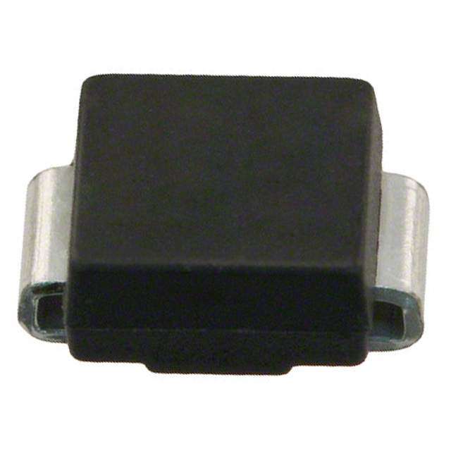
| 描述 | PWR LED SOURCE 1W GREEN INGAN |
| 产品分类 | |
| 品牌 | Avago Technologies US Inc. |
| 数据手册 | http://www.avagotech.com/docs/AV02-0129EN |
| 产品图片 | |
| 产品型号 | ASMT-MG00-NJK00 |
| rohs | 无铅 / 符合限制有害物质指令(RoHS)规范要求 |
| 产品系列 | - |
| 不同最大电流时的流明 | 60 lm |
| 不同测试电流时的流明/瓦 | 48 lm/W |
| 产品目录绘图 |
|
| 其它名称 | 516-2676-5 |
| 包装 | 管件 |
| 安装类型 | 表面贴装 |
| 封装/外壳 | TO-252-3,DPak(2 引线+接片),SC-63 |
| 封装热阻 | 10°C/W |
| 标准包装 | 500 |
| 波长 | 525nm (515nm ~ 535nm) |
| 电压-正向(Vf)(典型值) | 3.2V |
| 电压 -正向,最大电流时 | 3.2V |
| 电流-最大值 | 350mA |
| 电流-测试 | 350mA |
| 视角 | 120° |
| 颜色 | 绿 |




- 商务部:美国ITC正式对集成电路等产品启动337调查
- 曝三星4nm工艺存在良率问题 高通将骁龙8 Gen1或转产台积电
- 太阳诱电将投资9.5亿元在常州建新厂生产MLCC 预计2023年完工
- 英特尔发布欧洲新工厂建设计划 深化IDM 2.0 战略
- 台积电先进制程称霸业界 有大客户加持明年业绩稳了
- 达到5530亿美元!SIA预计今年全球半导体销售额将创下新高
- 英特尔拟将自动驾驶子公司Mobileye上市 估值或超500亿美元
- 三星加码芯片和SET,合并消费电子和移动部门,撤换高东真等 CEO
- 三星电子宣布重大人事变动 还合并消费电子和移动部门
- 海关总署:前11个月进口集成电路产品价值2.52万亿元 增长14.8%


PDF Datasheet 数据手册内容提取
ASMT-Mx00 MoonstoneTM 1 W Power LED Light Source Data Sheet Description Features The MoonstoneTM 1W Power LED Light Source is a high • Available in Red, Amber, Green, Blue, Cool White and Warm White color performance energy efficient device which can handle high thermal and high driving current. The exposed pad • Energy efficient design has excellent heat transfer from the package to • Exposed pad for excellent heat transfer the motherboard. • Suitable for reflow soldering process The Cool White Power LED is available in various color • High current operation temperature ranging from 4000K to 10000K and Warm • Long operation life White Power LED ranging from 2600K to 4000K. • Wide viewing angle The low profile package design is suitable for a wide • Silicone encapsulation variety of applications especially where height is a • ESD Class HBM Class 3B (threshold > 8 kV) constraint. • MSL 2A for InGaN products The package is compatible with reflow soldering • MSL 4 for AlInGaP products process. This will give more freedom and flexibility to the light source designer. Specifications Applications • AlInGaP technology for Red and Amber • Portable (flash light, bicycle head light) • 2.4 V (typ) at 350 mA for AlInGaP • InGaN technology for Green, Blue, Cool White and • Reading light Warm White • Architectural lighting • 3.6 V (typ) at 350 mA for InGaN • Garden lighting • 120 viewing angle • Decorative lighting
Package Dimensions 10.00 1 Anode 2 Cathode 3 Heat Sink 3.30 8.50 1.27 Metal Slug 3 Ø 5.26 LED + 10.60 ZENER 8.50 − Ø 8.00 2.00 5.25 1.30 1 2 0.81 5.08 Notes: 1. All dimensions are in millimeters. 2. Tolerance is ±0.1 mm unless otherwise specified. 3. Metal slug is connected to anode for electrically non-isolated option. Device Selection Guide ( T = 25°C) j Luminous Flux, f[1,2] (lm) V Test Current Dice Part Number Color Min. Typ. Max. (mA) Technology ASMT-MR00-AGH00 Red 25.5 35.0 43.0 350 AlInGaP ASMT-MR00-AHJ00 33.0 40.0 56.0 350 AlInGaP ASMT-MA00-AGH00 Amber 25.5 35.0 43.0 350 AlInGaP ASMT-MG00 Green 43.0 60.0 73.0 350 InGaN ASMT-MB00 Blue 11.5 15.0 25.5 350 InGaN ASMT-MW00 Cool White 43.0 60.0 73.0 350 InGaN ASMT-MY00 Warm White 43.0 50.0 73.0 350 InGaN ASMT-MWB1 Cool White Diffused 43.0 55.0 73.0 350 InGaN ASMT-MYB1 Warm White Diffused 43.0 46.0 73.0 350 InGaN Notes 1. f is the total luminous flux output as measured with an integrating sphere at 25 ms mono pulse condition. V 2. Flux tolerance is ± 10%. 2
Part Numbering System ASMT-M x xx – x x1 x2 x3 x4 Packaging Option Color Bin Selection Maximum Flux Bin Selection Minimum Flux Bin Selection Dice Type N – InGaN A – AllnGaP Silicone Type 00 – Non-diffused B1 – Diffused Color R – Red A – Amber G - Green B - Blue W - Cool White Y - Warm White Note: 1. Please refer to Page 8 for selection details. Absolute Maximum Ratings (T = 25°C) A Parameter ASMT-Mx00 / ASMT-MxB1 Units DC Forward Current [1] 350 mA Peak Pulsing Current [2] 1000 mA Power Dissipation for AlInGaP 1050 mW Power Dissipation for InGaN 1400 mW LED Junction Temperature for AlInGaP 125 °C LED Junction Temperature for InGaN 110 °C Operating Ambient Temperature Range -40 to +100 °C Storage Temperature Range -40 to +120 °C Notes: 1. DC forward current – derate linearly based on Figure 5 for AlInGaP & Figure 11 for InGaN. 2. Pulse condition duty factor = 10%, Frequency = 1kHz. 3
Optical Characteristics at 350 mA (T = 25°C) J Dominant Peak Wavelength Wavelength Viewing Angle Luminous l (nm) l [1] (nm) 2q [2] (°) Efficiency (lm/W) PEAK D 1/2 Part Number Color Typ. Typ. Typ. Typ. ASMT-MR00-AGH00 Red 635 625 120 42 ASMT-MR00-AHJ00 Red 635 625 120 48 ASMT-MA00-AGH00 Amber 598 590 120 42 ASMT-MG00 Green 519 525 120 48 ASMT-MB00 Blue 460 467 120 12 Correlated Color Temperature, Viewing Angle Luminous CCT (Kelvin) 2q [2] (°) Efficiency (lm/W) ½ Part Number Color Min. Max. Typ. Typ. ASMT-MW00 Cool White 4000 10000 110 48 ASMT-MY00 Warm White 2600 4000 110 40 ASMT-MWB1 Cool White Diffused 4000 10000 110 44 ASMT-MYB1 Warm White Diffused 2600 4000 110 37 Notes: 1. The dominant wavelength, l, is derived from the CIE Chromaticity Diagram and represents the color of the device. D 2. q is the off-axis angle where the luminous intensity is 1/2 the peak intensity. 1/2 Electrical Characteristic at 350 mA (T = 25°C) J Forward Voltage Reverse Voltage Thermal Resistance V (Volts) at I = 350mA V (Volts) Rq (°C/W) [1] F F R j-ms Dice Type Min Typ. Max. Max. Typ. AlInGaP 2.0 2.4 3.0 5 12 InGaN 3.2 3.6 4.0 5 10 Notes: 1. R is Thermal Resistance from LED junction to metal slug. qJ-ms 4
1.0 500 0.9 RED 450 AMBER 0.8 400 A Y0.7 m350 NSIT0.6 NT - 300 NTE0.5 RRE250 ELATIVE I00..34 WARD CU125000 R R 0.2 FO100 0.1 50 0.0 0 380 430 480 530 580 630 680 730 780 0.00 0.50 1.00 1.50 2.00 2.50 3.00 WAVELENGTH - nm FORWARD VOLTAGE - V Figure 1. Relative Intensity vs. Wavelength for AlInGaP Figure 2. Forward Current vs Forward Voltage for AlInGaP 1.4 1 0.9 1.2 m UX (-v) - l1.0 SITY00..78 S FL0.8 TEN0.6 U N0.5 MINO0.6 TIVE I0.4 U A VE L0.4 REL0.3 TI 0.2 LA0.2 RE 0.1 0.0 0 0 50 100 150 200 250 300 350 400 450 500 -90 -70 -50 -30 -10 10 30 50 70 90 MONO PULSE CURRENT - mA OFF-AXIS ANGLE(°) Figure 3. Relative Luminous Flux vs. Mono Pulse Current for AlInGaP Figure 4. Radiation Pattern for AlInGaP 400 2 350 C) RED FORWARD CURRENT - mA 122350500000 RJA = 60R°CJ/AW = 50°CR/WJA = 40°C/W OP (Normalized at 25° 1.51 AMBER MAX 100 VE L 0.5 I- F 50 LATI E R 0 0 0 10 20 30 40 50 60 70 80 90 -40 -25 -10 5 20 35 50 65 80 95 110 125 T - AMBIENT TEMPERATURE - °C A JUNCTION TEMPERATURE - °C Figure 5. Maximum forward current vs. ambient temperature for AlInGaP Figure 6. Relative LOP (Normalized at 25°C) vs. junction temperature for Derated based on TMAX = 125°C, Rθ = 40°C/W / 50°C/W and 60°C/W AlInGaP J JA 5
1.0 500 GREEN 0.9 450 BLUE 0.8 COOL WHITE 400 Y0.7 WARM WHITE mA350 SIT T - N0.6 N300 E E T R N0.5 R250 E I CU TIV0.4 RD 200 A A EL0.3 W150 R R O 0.2 F100 0.1 50 0.0 0 380 430 480 530 580 630 680 730 780 0.00 0.50 1.00 1.50 2.00 2.50 3.00 3.50 4.00 WAVELENGTH - nm FORWARD VOLTAGE - V Figure 7. Relative Intensity vs. Wavelength for InGaN Figure 8. Forward Current vs. Forward Voltage for InGaN 1.4 1.0 0.9 m 1.2 V) - l 0.8 US FLUX (φ 01..80 NTENSITY000...567 NO 0.6 E I MI TIV0.4 GREEN U A VE L 0.4 REL0.3 BLUE LATI 0.2 0.2 COOL WHITE RE 0.1 WARM WHITE 0.0 0.0 0 5 0 100 150 200 250 300 350 400 450 500 -90 -70 -50 -30 -10 10 30 50 70 90 MONO PULSE CURRENT - mA OFF-AXIS ANGLE (°) Figure 9. Relative Luminous Flux vs Mono Pulse Current for InGaN Figure 10. Radiation Pattern for InGaN 400 540 A m GREEN – 350 530 WARD CURRENT 322005000 RRθθJJAA == 5400 CC//WW VELENGTH – nm555012000 OR RθJA = 30 C/W WA490 M F150 NT 480 AXIMU100 OMINA470 BLUE – M 50 D460 F I 0 450 0 10 20 30 40 50 60 70 80 90 100 150 200 250 300 350 400 TA – AMBIENT TEMPERATURE – °C FORWARD CURRENT – mA Figure 11. Maximum Forward Current vs. Ambient Temperature for InGaN Figure 12. Dominant wavelength vs. forward current – InGaN devices Derated based on TMAX = 110°C, Rq = 30°C/W, 40°C/W and 50°C/W J JA 6
0.016 100 mA 0.014 150 mA 0.012 ES 0.01 T A N DI0.008 250 mA R O O0.006 C Y- 0.004 300 mA 0.002 350 mA 0 0 0.001 0.002 0.003 0.004 0.005 0.006 0.007 0.008 X-COORDINATES Figure 13. Chromaticity shift vs. current *Note: (x,y) values @ 350 mA reference to (0.0) 10.70 ± 0.10 10 - 30 SEC. 255 - 260 °C 217 °C 3 °C/SEC. MAX. 8.40 ± 0.10 E 200 °C -6 °C/SEC. MAX. R U AT 17.00 ± 0.20 R 150 °C E P M 3 °C/SEC. MAX. E 1.00 ± 0.10 T 60 - 120 SEC. 100 SEC. MAX. 3.1 ± 0.10 TIME 5.08 ± 0.10 (Acc. to J-STD-020C) Figure 14. Recommended reflow soldering profile Figure 15. Recommended soldering land pattern 300 100 mV)250 90 FT (200 80 HI150 S 70 GE 100 %) LTA 50 OP (60 VO 0 E L50 RD -50 TIV40 A A RW-100 REL30 GREEN O BLUE F-150 E 20 COOL WHITE LATIV--225000 10 WARM WHITE E R-300 0 -40 -15 10 35 60 85 25 30 35 40 45 50 55 60 65 70 75 80 85 90 95 100105110 TEMPERATURE - °C JUNCTION TEMPERATURE (°C) Figure 16. Temperature vs. relative forward voltage shift Figure 17. Relative LOP vs Junction Temperature for InGaN Devices Note: For detail information on reflow soldering of Avago surface mount LEDs, do refer to Avago Application Note AN1060 Surface Mounting SMT LED Indicator Components. 7
Option Selection Details Flux Bin Limit [x x] 1 2 ASMT-Mxxx – x x x x x Luminous Flux (lm) at I = 350mA 1 2 3 4 F x – Minimum Flux Bin Selection Bin Min. Max. 1 x – Maximum Flux Bin Selection D 11.5 15.0 2 x – Color Bin Selection E 15.0 19.5 3 x – Packaging Option F 19.5 25.5 4 G 25.5 33.0 H 33.0 43.0 J 43.0 56.0 K 56.0 73.0 Tolerance for each bin limits is ±10% Color Bin Selection [x ] 3 Individual reel will contain parts from one full bin only. Warm White Cool White 0 Full Distribution 0 Full Distribution A A only A A only B B only B B only C C only C C only D D only D D only E E only E E only F F only F F only N A and C only G G only P B and D only H H only Q E and C only L A and G only R F and D only M B and H only U E and F only N A and C only W C and D only P B and D only Z A and B only Q E and C only 1 A, B, C and D only R F and D only 4 C, D, E and F only S G and H only U E and F only Other Colors W C and D only 0 Full Distribution Z A and B only Z A and B 1 A, B, C and D only Y B and C 2 G, H, A and B only 4 C, D, E and F only W C and D V D and E Q A, B and C P B, C and D N C, D and E 8
0.44 0.48 0.42 0.46 0.40 G 0.44 0.38 Y - COORDINATE 0000....33330246 E 7kC D 5.6kBA 4H.5k 4.0Bklack Body Curve Y - COORDINATE000...344802 4.F0k E 3.5Dk C 3.0Bk A B2.l6akck Body Curve 0.36 0.28 10k F 0.34 0.26 0.24 0.32 0.24 0.26 0.28 0.30 0.32 0.34 0.36 0.38 0.40 0.42 0.44 0.34 0.36 0.38 0.40 0.42 0.44 0.46 0.48 0.50 0.52 X - COORDINATE X - COORDINATE Figure 18. Color bins (Cool White). Figure 19. Color bins (Warm White). Color Bin Limits Warm Color Limits Cool Color Limits White (Chromaticity Coordinates) White (Chromaticity Coordinates) Bin A x 0.452 0.488 0.470 0.438 Bin A x 0.367 0.362 0.329 0.329 y 0.434 0.447 0.414 0.403 y 0.400 0.372 0.345 0.369 Bin B x 0.438 0.470 0.452 0.424 Bin B x 0.362 0.356 0.329 0.329 y 0.403 0.414 0.384 0.376 y 0.372 0.330 0.302 0.345 Bin C x 0.407 0.418 0.452 0.438 Bin C x 0.329 0.329 0.305 0.301 y 0.393 0.422 0.434 0.403 y 0.369 0.345 0.322 0.342 Bin D x 0.395 0.407 0.438 0.424 Bin D x 0.329 0.329 0.311 0.305 y 0.362 0.393 0.403 0.376 y 0.345 0.302 0.285 0.322 Bin E x 0.381 0.387 0.418 0.407 Bin E x 0.303 0.307 0.283 0.274 y 0.377 0.404 0.422 0.393 y 0.333 0.311 0.284 0.301 Bin F x 0.373 0.381 0.407 0.395 Bin F x 0.307 0.311 0.290 0.283 y 0.349 0.377 0.393 0.362 y 0.311 0.285 0.265 0.284 Tolerance: ± 0.01 Bin G x 0.388 0.379 0.362 0.367 y 0.417 0.383 0.372 0.400 Color Bin Min. Max. Bin H x 0.379 0.369 0.356 0.362 y 0.383 0.343 0.330 0.372 Red Full Distribution 620.0 635.0 Tolerance: ± 0.01 Amber A 582.0 584.5 B 584.5 587.0 C 587.0 589.5 D 589.5 592.0 E 592.0 594.5 Blue A 460.0 465.0 B 465.0 470.0 C 470.0 475.0 D 475.0 480.0 Green A 515.0 520.0 B 520.0 525.0 C 525.0 530.0 D 530.0 535.0 Tolerance: ± 1 nm 9
Sub-Color Binning (Only Applicable for Color Bin A to Bin D and Bin G to Bin H) Color Limits Cool White (Chromaticity Coordinates) Cool White (Chromaticity Coordinates) Bin A1 X 0.364 0.367 0.348 0.347 Bin D1 X 0.329 0.329 0.317 0.316 Y 0.383 0.400 0.385 0.372 Y 0.345 0.331 0.320 0.333 Bin A2 X 0.364 0.362 0.346 0.347 Bin D2 X 0.329 0.329 0.318 0.317 Y 0.383 0.372 0.359 0.372 Y 0.331 0.320 0.310 0.320 Bin A3 X 0.329 0.329 0.348 0.347 Bin D3 X 0.329 0.329 0.320 0.318 Y 0.357 0.369 0.385 0.372 Y 0.320 0.302 0.293 0.310 Bin A4 X 0.329 0.329 0.347 0.346 Bin D4 X 0.316 0.317 0.307 0.305 Y 0.345 0.357 0.372 0.359 Y 0.333 0.320 0.311 0.322 Bin B1 X 0.362 0.360 0.344 0.346 Bin D5 X 0.317 0.318 0.309 0.307 Y 0.372 0.357 0.344 0.359 Y 0.320 0.310 0.300 0.311 Bin B2 X 0.360 0.358 0.343 0.344 Bin D6 X 0.318 0.320 0.311 0.309 Y 0.357 0.343 0.331 0.344 Y 0.310 0.293 0.285 0.300 Bin B3 X 0.358 0.356 0.341 0.343 Bin G1 X 0.392 0.386 0.364 0.367 Y 0.343 0.330 0.314 0.331 Y 0.421 0.400 0.383 0.400 Bin B4 X 0.329 0.329 0.346 0.344 Bin G2 X 0.386 0.382 0.362 0.364 Y 0.331 0.345 0.359 0.344 Y 0.400 0.385 0.372 0.383 Bin B5 X 0.329 0.344 0.343 0.329 Bin H1 X 0.382 0.378 0.360 0.362 Y 0.331 0.344 0.331 0.320 Y 0.385 0.370 0.357 0.372 Bin B6 X 0.343 0.341 0.329 0.329 Bin H2 X 0.378 0.375 0.358 0.360 Y 0.331 0.314 0.302 0.320 Y 0.370 0.358 0.343 0.357 Bin C1 X 0.329 0.329 0.315 0.314 Bin H3 X 0.375 0.371 0.356 0.358 Y 0.369 0.357 0.344 0.355 Y 0.358 0.344 0.330 0.343 Bin C2 X 0.329 0.329 0.316 0.315 Tolerances ±0.01 Y 0.357 0.345 0.333 0.344 Bin C3 X 0.314 0.315 0.303 0.301 Y 0.355 0.344 0.333 0.342 Bin C4 X 0.315 0.316 0.305 0.303 Y 0.344 0.333 0.322 0.333 0.44 0.42 0.40 G1 A1 G2 0.38 A3 A2 H1 4.0k ATE 0.36 C1 A4 B1 4.5kH2 N DI 0.34 C3 C2 B4 B2 H3 OOR C4 D1 B55.6k B3 Black Body Curve Y - C 0.32 D4 D2 B6 7k D5 D3 0.30 D6 0.28 10k 0.26 0.24 0.24 0.26 0.28 0.30 0.32 0.34 0.36 0.38 0.40 0.42 0.44 X - COORDINATE Figure 20. Sub-color bins (Cool White) 10
Packaging option [x] Example 4 Selection Option ASMT-MR00-AHJ00 0 Tube ASMT-MR00-Axxxx – AllnGaP Red, Non-diffused x = H – Minimum Flux Bin H 1 Tape & Reel 1 x = J – Maximum Flux Bin J 2 x = 0 – Full Distribution 3 x = 0 – Tube Option 4 Packing Tube - Option 0 1.00 5.80 4.65 5.50 37.00 5.45 10.10 8.30 535.00 SIDE VIEW TOP VIEW Figure 21. Tube dimensions Tape & Reel - Option 1 Tape Dimension A E Dim Value A0 8.80±0.10 F B0 16.45±0.10 W o B K0 3.60±0.10 W 24.0±0.10 B B P 16.0±0.10 5 A 2. Qty/Reel 250EA Ko Unit: mm P SECTION A Ao SECTION B Figure 22. Carrier tape dimensions
Tape & Reel - Option 1 (Cont.) Tape Dimension END START THERE SHALL BE A MINIMUM OF MOUNTED WITH THERE SHALL BE A MINIMUM OF 390 mm OF EMPTY 160 mm OF EMPTY COMPONENT COMPONENTS COMPONENT POCKETS SEALED WITH COVER TAPE. POCKETS SEALED WITH COVER TAPE. Figure 23. Carrier tape leader and trailer dimensions Reel Dimensions 24.0+1.00 −0.00 2.30 2.30 R10.00 0 0 1. ± 0 5 9. 9∅ 2.50 ± 0.50 6 0.0º ∅268.00 R10.50 ± 0.50 ∅13.50 ± 0.50 ∅330.00 ± 1.00 Figure 24. Reel dimensions 120.0º
Handling Precaution The encapsulation material of the product is made of sili- B. Control after opening the MBB cone for better reliability of the product. As silicone is a • The humidity indicator card (HIC) shall be read soft material, please do not press on the silicone or poke immediately upon opening of MBB. a sharp object onto the silicone. These might damage • The LEDs must be kept at <30°C/60%RH at all time the product and cause premature failure. During as- and all high temperature related process including sembly or handling, the unit should be held on the body soldering, curing or rework need to be completed only. Please refer to Avago Application Note AN5288 for within 672 hours for MSL 2a and 72 hours for MSL detail information. 4. Moisture Sensitivity C. Control for unfinished reel This product is qualified as Moisture Sensitive Level 2a • For any unused LEDs, they need to be stored for InGaN devices and MSL 4 for AlInGaP devices per in sealed MBB with desiccant or desiccator at Jedec J-STD-020. Precautions when handling this mois- <5%RH. ture sensitive product is important to ensure the reliabil- D. Control of assembly boards ity of the product. Do refer to Avago Application Note • If the PCB soldered with the LEDs is to be subjected AN5305 Handling of Moisture Sensitive Surface Mount to other high temperature processes, the PCB Devices for details. need to be stored in sealed MBB with desiccant A. Storage before use or desiccator at <5%RH to ensure no LEDs have • Unopen moisture barrier bag (MBB) can be stored exceeded their floor life of 672 hours for MSL 2a at <40°C/90%RH for 12 months. If the actual shelf and 72 hours for MSL 4. life has exceeded 12 months and the humidity E. Baking is required if indicator card (HIC) indicates that baking is not • HIC “10%” indicator is not blue and “5%” indicator required, then it is safe to reflow the LEDs per the is pink. - The LEDs are exposed to condition of original MSL rating. >30°C/60% RH at any time. • It is not recommended to open the MBB prior to • The LEDs floor life exceeded 672 hours for MSL 2a assembly (e.g. for IQC). and 72 hours for MSL 4. Recommended baking condition: 60±5ºC for 20hrs. DISCLAIMER AVAGO’S PRODUCTS AND SOFTWARE ARE NOT SPECIFICALLY DESIGNED, MANUFACTURED OR AUTHORIZED FOR SALE AS PARTS, COMPONENTS OR ASSEMBLIES FOR THE PLANNING, CONSTRUCTION, MAINTENANCE OR DIRECT OP- ERATION OF A NUCLEAR FACILITY OR FOR USE IN MEDICAL DEVICES OR APPLICATIONS. CUSTOMER IS SOLELY RE- SPONSIBLE, AND WAIVES ALL RIGHTS TO MAKE CLAIMS AGAINST AVAGO OR ITS SUPPLIERS, FOR ALL LOSS, DAMAGE, EXPENSE OR LIABILITY IN CONNECTION WITH SUCH USE. For product information and a complete list of distributors, please go to our web site: www.avagotech.com Avago, Avago Technologies, and the A logo are trademarks of Avago Technologies in the United States and other countries. Data subject to change. Copyright © 2005-2009 Avago Technologies. All rights reserved. Obsoletes AV01-0668EN AV02-0129EN - September 2, 2009

 Datasheet下载


