ICGOO在线商城 > 射频/IF 和 RFID > RFID,RF 接入,监控 IC > AS3933-BTST
 Datasheet下载
- 型号: AS3933-BTST
- 制造商: AUSTRIAMICROSYSTEMS
- 库位|库存: xxxx|xxxx
- 要求:
| 数量阶梯 | 香港交货 | 国内含税 |
| +xxxx | $xxxx | ¥xxxx |
查看当月历史价格
查看今年历史价格
AS3933-BTST产品简介:
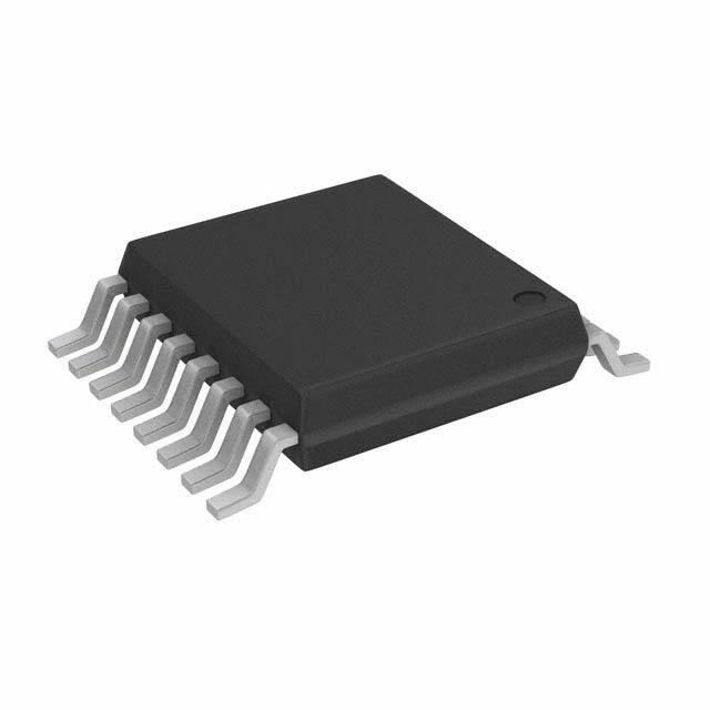
ICGOO电子元器件商城为您提供AS3933-BTST由AUSTRIAMICROSYSTEMS设计生产,在icgoo商城现货销售,并且可以通过原厂、代理商等渠道进行代购。 AS3933-BTST价格参考¥21.64-¥36.54。AUSTRIAMICROSYSTEMSAS3933-BTST封装/规格:RFID,RF 接入,监控 IC, RFID Reader IC 15kHz ~ 150kHz 2.4 V ~ 3.6 V 16-TSSOP (0.173", 4.40mm Width)。您可以下载AS3933-BTST参考资料、Datasheet数据手册功能说明书,资料中有AS3933-BTST 详细功能的应用电路图电压和使用方法及教程。
AS3933-BTST 是奥地利微电子公司(ams)推出的一款高性能、低功耗的RFID接收器集成电路,专为无源超高频(UHF)RFID系统设计。它主要应用于RFID标签读取和监控场景,具备高灵敏度和快速响应的特点。以下是该芯片的主要应用场景:

1. 资产管理与追踪:AS3933-BTST 可用于仓库、物流中心等场所,帮助实时追踪资产的位置和状态。通过安装在固定或移动设备上的读写器,可以实现对货物、工具、设备等物品的高效管理,减少丢失和损坏的风险。

2. 智能仓储与供应链管理:在自动化仓库中,AS3933-BTST 能够配合RFID标签实现库存盘点、出入库记录等功能。它可以大幅提高数据采集的速度和准确性,优化库存水平,降低运营成本。

3. 门禁控制与安全防护:该芯片也可用于构建基于RFID的身份验证系统,如企业园区、办公楼宇等场合的门禁控制系统。凭借其强大的信号处理能力,确保只有授权人员才能进入特定区域,提升安全性。

4. 工业自动化与智能制造:在工厂流水线、生产线等环境中,AS3933-BTST 有助于实现对原材料、半成品及成品的全程跟踪,支持精益生产和智能制造理念的应用。此外,它还能与其他传感器结合使用,提供更丰富的环境感知功能。

5. 零售行业应用:超市、商场等零售场景下,AS3933-BTST 支持自助结账、防伪溯源等功能,改善顾客购物体验的同时也增强了商品管理效率。

总之,AS3933-BTST 凭借其卓越的性能,在多个领域有着广泛的应用前景,能够有效提升系统的智能化水平和服务质量。
| 参数 | 数值 |
| 产品目录 | |
| 描述 | IC RECEIVER ASK 3CH LP 16TSSOPRFID应答器 3D Low Power Wakeup Receiver |
| 产品分类 | RFID IC集成电路 - IC |
| 品牌 | ams |
| 产品手册 | |
| 产品图片 |
|
| rohs | 符合RoHS无铅 / 符合限制有害物质指令(RoHS)规范要求 |
| 产品系列 | RF集成电路,RFID应答器,ams AS3933-BTST- |
| 数据手册 | |
| 产品型号 | AS3933-BTST |
| RF类型 | 接收器 |
| 产品种类 | RFID应答器 |
| 供应商器件封装 | 16-TSSOP |
| 其它名称 | AS3933-BTSTDKR |
| 包装 | Digi-Reel® |
| 商标 | ams |
| 安装风格 | SMD/SMT |
| 封装 | Reel |
| 封装/外壳 | 16-TSSOP(0.173",4.40mm 宽) |
| 封装/箱体 | TSSOP-16 |
| 工厂包装数量 | 1000 |
| 最大工作温度 | + 85 C |
| 最小工作温度 | - 40 C |
| 标准包装 | 1 |
| 特性 | - |
| 类型 | RF Receiver |
| 频率 | 15kHz ~ 150kHz |


- 商务部:美国ITC正式对集成电路等产品启动337调查
- 曝三星4nm工艺存在良率问题 高通将骁龙8 Gen1或转产台积电
- 太阳诱电将投资9.5亿元在常州建新厂生产MLCC 预计2023年完工
- 英特尔发布欧洲新工厂建设计划 深化IDM 2.0 战略
- 台积电先进制程称霸业界 有大客户加持明年业绩稳了
- 达到5530亿美元!SIA预计今年全球半导体销售额将创下新高
- 英特尔拟将自动驾驶子公司Mobileye上市 估值或超500亿美元
- 三星加码芯片和SET,合并消费电子和移动部门,撤换高东真等 CEO
- 三星电子宣布重大人事变动 还合并消费电子和移动部门
- 海关总署:前11个月进口集成电路产品价值2.52万亿元 增长14.8%


PDF Datasheet 数据手册内容提取
Datasheet AS3933 3D Low Frequency Wakeup Receiver 1 General Description (cid:132) Wakeup sensitivity 80 µVRMS (typ) (cid:132) Adjustable sensitivity level The AS3933 is a 3-channel low power ASK receiver that is able to (cid:132) Highly resistant to false wakeups generate a wakeup upon detection of a data signal which uses a LF carrier frequency between 15-150 kHz. The integrated correlator can (cid:132) Easy antenna tuning for perfect matching on the wanted carrier be used for detection of a programmable 16-bit or 32-bit Manchester frequency wakeup pattern. The device can operate using one, two, or three (cid:132) Self calibration of the internal RC-oscillator active channels. (cid:132) False wakeup counter The AS3933 provides a digital RSSI value for each active channel, it supports a programmable data rate and Manchester decoding with (cid:132) Periodical forced wakeup supported (1s – 2h) clock recovery. The AS3933 offers an internal Clock Generator, (cid:132) Low power listening modes which is either derived from a crystal oscillator or the internal RC oscillator. The user can decide to use the external clock generator (cid:132) Current consumption in 3-channel listening mode 1.7 µA (typ) instead. (cid:132) Data rate adjustable from 0.5- 4 kbps (Manchester) The programmable features of AS3933 enable to optimize its (cid:132) Manchester decoding with clock recovery settings for achieving a longer distance while retaining a reliable wakeup generation. The sensitivity level of AS3933 can be adjusted (cid:132) Digital RSSI values available for each channel in presence of a strong field or in noisy environments. (cid:132) Dynamic range 64dB Antenna tuning is greatly simplified, as the automatic tuning feature (cid:132) 5-bit RSSI step (2dB per step) ensures perfect matching to the desired carrier frequency. (cid:132) Clock Generator based on 32kHz XTAL, RC-OSC, or External The device is available in 16 pin TSSOP and QFN 4x4 16LD Clock packages. (cid:132) Operating temperature range -40 to +85ºC (cid:132) Operating supply voltage 2.4 - 3.6V (TA = 25ºC) 2 Key Features (cid:132) Bidirectional serial peripheral interface (SPI) (cid:132) 3-channel ASK wakeup receiver (cid:132) Package option: 16 pin TSSOP, QFN 4x4 16LD (cid:132) Carrier frequency range 15 - 150 kHz 3 Applications (cid:132) One, two, or three channel operation (cid:132) Reliable 1-, 2- or 3-D wakeup pattern detection The AS3933 is ideal for Active RFID tags, Real-time location systems, Operator identification, Access control, and Wireless (cid:132) Programmable wakeup pattern (16-bit or 32-bit) Manchester sensors. (cid:132) Doubling of wakeup pattern supported (both for 16 and 32 bits) (cid:132) Wakeup without pattern detection supported www.austriamicrosystems.com/LF-Receiver/AS3933 Revision 1.2 1 - 42
AS3933 Datasheet - Applications Figure 1. AS3933 Typical Application Diagram with Crystal Oscillator VCC VCC CS CBAT CL CL XIN CL_DAT XTAL XOUT DAT a n TRANSMITTER en TX ansmitting Ant ving Antennas LLFF12PP AS3933 WASKCEL Tr cei e R LF3P SDO Z d n a Y, LFN SDI X, VSS GND Figure 2. AS3933 Typical Application Diagram with RC Oscillator VCC VCC CS CBAT XIN CL_DAT XOUT DAT a n TRANSMITTER en TX ansmitting Ant ving Antennas LLFF12PP AS3933 WASKCEL Tr cei e R LF3P SDO Z d n a Y, LFN SDI X, VSS GND www.austriamicrosystems.com/LF-Receiver/AS3933 Revision 1.2 2 - 42
AS3933 Datasheet - Applications Figure 3. AS3933 Typical Application Diagram with Clock from External Source VCC VCC CS CBAT XIN CL_DAT EXT. CLOCK XOUT DAT a n TRANSMITTER en TX ansmitting Ant ving Antennas LLFF12PP AS3933 WASKCEL Tr cei e R LF3P SDO Z d n a Y, LFN SDI X, VSS GND www.austriamicrosystems.com/LF-Receiver/AS3933 Revision 1.2 3 - 42
AS3933 Datasheet - Contents Contents 1 General Description.................................................................................................................................................................. 1 2 Key Features............................................................................................................................................................................. 1 3 Applications............................................................................................................................................................................... 1 4 Pin Assignments....................................................................................................................................................................... 5 4.1 TSSOP-16 Package............................................................................................................................................................................. 5 4.1.1 Pin Descriptions........................................................................................................................................................................... 5 4.2 QFN-16 Package.................................................................................................................................................................................. 6 4.2.1 Pin Descriptions........................................................................................................................................................................... 6 5 Absolute Maximum Ratings...................................................................................................................................................... 7 6 Electrical Characteristics........................................................................................................................................................... 8 7 Typical Operating Characteristics........................................................................................................................................... 11 8 Detailed Description................................................................................................................................................................ 12 8.1 Operating Modes................................................................................................................................................................................ 13 8.1.1 Listening Mode.......................................................................................................................................................................... 14 8.1.2 Artificial Wakeup........................................................................................................................................................................ 15 8.1.3 Preamble Detection / Pattern Correlation.................................................................................................................................. 15 8.1.4 Data Receiving.......................................................................................................................................................................... 15 8.2 System and Block Specification......................................................................................................................................................... 16 8.2.1 Register Table........................................................................................................................................................................... 16 8.2.2 Register Table Description and Default Values......................................................................................................................... 16 8.2.3 Serial Peripheral Interface (SPI)................................................................................................................................................ 18 8.2.4 SDI Timing................................................................................................................................................................................. 22 8.3 Channel Amplifier, Frequency Detector and RSSI............................................................................................................................. 22 8.3.1 Frequency Detector / RSSI / Channel Selector......................................................................................................................... 23 8.3.2 Antenna Damper........................................................................................................................................................................ 24 8.4 Demodulator / Data Slicer.................................................................................................................................................................. 25 8.5 Correlator............................................................................................................................................................................................ 27 8.5.1 Pattern: Bit and Symbol Definition in Manchester Code............................................................................................................ 27 8.6 Wakeup Protocol................................................................................................................................................................................ 29 8.6.1 Wakeup Protocol: Frequency Detection Only............................................................................................................................ 30 8.6.2 Wakeup Protocol: Pattern Detection Enabled........................................................................................................................... 30 8.6.3 Manchester Decoder and Clock Recovery................................................................................................................................ 32 8.7 False Wakeup Register...................................................................................................................................................................... 32 8.8 Clock Generator................................................................................................................................................................................. 34 8.8.1 Crystal Oscillator........................................................................................................................................................................ 34 8.8.2 RC-Oscillator............................................................................................................................................................................. 35 8.8.3 External Clock Source............................................................................................................................................................... 36 8.9 Antenna Tuning.................................................................................................................................................................................. 36 8.10 Channel Selection in Scanning Mode and ON/OFF Mode............................................................................................................... 37 9 Package Drawings and Markings........................................................................................................................................... 38 10 Ordering Information............................................................................................................................................................. 41 www.austriamicrosystems.com/LF-Receiver/AS3933 Revision 1.2 4 - 42
AS3933 Datasheet - Pin Assignments 4 Pin Assignments 4.1 TSSOP-16 Package Figure 4. TSSOP Pin Assignments (Top View) CS 1 16 CL_DAT SCL 2 15 DAT SDI 3 14 WAKE SDO 4 13 VSS AS3933 VCC 5 12 XOUT GND 6 11 XIN LF3P 7 10 LFN LF2P 8 9 LF1P 4.1.1 Pin Descriptions Table 1. TSSOP-16 Pin Descriptions Pin Name Pin Number Pin Type Description CS 1 Chip select SCL 2 Digital input SDI interface clock SDI 3 SDI data input SDO 4 Digital output / tristate SDI data output (tristate when CS is low) VCC 5 Positive supply voltage Supply pad GND 6 Negative supply voltage LF3P 7 Input antenna channel three LF2P 8 Input antenna channel two LF1P 9 Input antenna channel one Analog I/O LFN 10 Common ground for antenna one, two and three XIN 11 Crystal oscillator input XOUT 12 Crystal oscillator output VSS 13 Supply pad Substrate WAKE 14 Wakeup output IRQ DAT 15 Digital output Data output CL_DAT 16 Manchester recovered clock www.austriamicrosystems.com/LF-Receiver/AS3933 Revision 1.2 5 - 42
AS3933 Datasheet - Pin Assignments 4.2 QFN-16 Package Figure 5. QFN Pin Assignments (Top View) ND CC DO DI G V S S 16 15 14 13 LF3P 1 12 SCL LF2P 2 11 CS AS3933 LF1P 3 10 CL_DAT LFN 4 9 DAT 5 6 7 8 XIN XOUT VSS WAKE 4.2.1 Pin Descriptions Table 2. QFN-16 Pin Descriptions Pin Name Pin Number Pin Type Description LF3P 1 Input antenna channel three LF2P 2 Input antenna channel two LF1P 3 Input antenna channel one Analog I/O LFN 4 Common ground for antenna one, two and three XIN 5 Crystal oscillator input XOUT 6 Crystal oscillator output VSS 7 Supply pad Substrate WAKE 8 Wakeup output IRQ DAT 9 Digital output Data output CL_DAT 10 Manchester recovered clock CS 11 Chip select SCL 12 Digital input SDI interface clock SDI 13 SDI data input SDO 14 Digital output / tristate SDI data output (tristate when CS is low) VCC 15 Positive supply voltage Supply pad GND 16 Negative supply voltage www.austriamicrosystems.com/LF-Receiver/AS3933 Revision 1.2 6 - 42
AS3933 Datasheet - Absolute Maximum Ratings 5 Absolute Maximum Ratings Stresses beyond those listed in Table 3 may cause permanent damage to the device. These are stress ratings only, and functional operation of the device at these or any other conditions beyond those indicated in Electrical Characteristics on page 8 is not implied. Exposure to absolute maximum rating conditions for extended periods may affect device reliability. Table 3. Absolute Maximum Ratings Parameter Min Max Units Comments Electrical Parameters DC supply voltage (VDD) -0.5 5 V Input pin voltage (VIN) -0.5 5 V Input current (latch up immunity) (ISOURCE) -100 100 mA Norm: Jedec 78 Electrostatic Discharge Electrostatic discharge (ESD) ±2 kV Norm: MIL 883 E method 3015 (HBM) Continuous Power Dissipation Total power dissipation 0.07 mW (all supplies and outputs) (Pt) Temperature Ranges and Storage Conditions Storage temperature (Tstrg) -65 150 ºC Norm: IPC/JEDEC J-STD-020 The reflow peak soldering temperature (body Package body temperature (Tbody) 260 ºC temperature) is specified according IPC/JEDEC J- STD-020 “Moisture/Reflow Sensitivity Classification for Non-hermetic Solid State Surface Mount Devices”. Humidity non-condensing 5 85 % www.austriamicrosystems.com/LF-Receiver/AS3933 Revision 1.2 7 - 42
AS3933 Datasheet - Electrical Characteristics 6 Electrical Characteristics Table 4. Operating Conditions Symbol Parameter Conditions Min Typ Max Units AVDD Positive supply voltage 2.4 3 3.6 V AVSS Negative supply voltage 0 0 V TAMB Ambient temperature -40 85 ºC Table 5. DC/AC Characteristics for Digital Inputs and Outputs Symbol Parameter Conditions Min Typ Max Units CMOS Input 0.6 * 0.7 * VIH High level input voltage VDD VDD 0.8 * VDD V 0.12 * 0.2 * 0.3 * VIL Low level input voltage VDD VDD DVDD V ILEAK Input leakage current 100 nA CMOS Output VOH High level output voltage With a load current of 1mA V0D.D4 - V VOL Low level output voltage With a load current of 1mA VSS + 0.4 V CL Capacitive load For a clock frequency of 1 MHz 400 pF Tristate CMOS Output VOH High level output voltage With a load current of 1mA V0D.D4 - V VOL Low level output voltage With a load current of 1mA VSS + 0.4 V IOZ Tristate leakage current to DVDD and DVSS 100 nA Table 6. Electrical System Specifications Symbol Parameter Conditions Min Typ Max Units Input Characteristics In case no antenna damper is set RIN AC Input Impedance at125kHz (R1<4>=0) 2 MΩ F1max Maximum Input Frequency Band1 150 kHz F1min Minimum Input Frequency Band1 95 kHz F2max Maximum Input Frequency Band2 95 kHz F2min Minimum Input Frequency Band2 65 kHz F3max Maximum Input Frequency Band3 65 kHz F3min Minimum Input Frequency Band3 40 kHz F4max Maximum Input Frequency Band4 40 kHz F4min Minimum Input Frequency Band4 23 kHz F5max Maximum Input Frequency Band5 23 kHz F5min Minimum Input Frequency Band5 15 kHz www.austriamicrosystems.com/LF-Receiver/AS3933 Revision 1.2 8 - 42
AS3933 Datasheet - Electrical Characteristics Table 6. Electrical System Specifications Symbol Parameter Conditions Min Typ Max Units Current Consumption Current Consumption in standard I1CHRC listening mode with one active channel 2.7 µA and RC-oscillator as Clock Generator Current Consumption in standard I2CHRC listening mode with two active channels 4.2 µA and RC-oscillator as Clock Generator Current Consumption in standard listening mode with three active I3CHRC 5.7 µA channels and RC-oscillator as Clock Generator Current Consumption in scanning I3CHSCRC mode with three active channels and 2.7 µA RC-oscillator as Clock Generator Current Consumption in ON/OFF mode 11% Duty Cycle 1.7 I3CHOORC with three active channels and RC- µA oscillator as Clock Generator 50% Duty Cycle 3.45 Current Consumption in standard listening mode with three active I3CHXT 6.5 8.9 µA channels and crystal oscillator as Clock Generator Current Consumption in Preamble With 125 kHz carrier frequency and 1 kbps IDATA detection / Pattern correlation / Data 8.3 12 µA data-rate. No load on the output pins. receiving mode (RC-oscillator) Additional current consumption per IBOOST 150 nA channel if gain boost enabled Input Sensitivity With 125 kHz carrier frequency, chip in Input Sensitivity on all channels in the SENS1 default mode, 4 half bits burst + 4 symbols 100 µVrms Band1 preamble and single preamble detection With 125 kHz carrier frequency, chip in Input Sensitivity on all channels in the SENS1B default mode, 4 half bits burst + 4 symbols 80 µVrms Band1 with 3dB gain boost preamble and single preamble detection With 90 kHz carrier frequency, chip in Input Sensitivity on all channels in the SENS2 default mode, 4 half bits burst + 4 symbols 100 µVrms Band2 preamble and single preamble detection With 90 kHz carrier frequency, chip in Input Sensitivity on all channels in the SENS2B default mode, 4 half bits burst + 4 symbols 80 µVrms Band2 with 3dB gain boost preamble and single preamble detection With 60 kHz carrier frequency, chip in Input Sensitivity on all channels in the SENS3 default mode, 4 half bits burst + 4 symbols 100 µVrms Band3 preamble and single preamble detection With 60 kHz carrier frequency, chip in Input Sensitivity on all channels in the SENS3B default mode, 4 half bits burst + 4 symbols 80 µVrms Band3 with 3dB gain boost preamble and single preamble detection With 30 kHz carrier frequency, chip in Input Sensitivity on all channels in the SENS4B default mode, 4 half bits burst + 4 symbols 80 µVrms Band4 with 3dB gain boost preamble and single preamble detection With 18 kHz carrier frequency, chip in Input Sensitivity on all channels in the SENS5B default mode, 4 half bits burst + 4 symbols 80 Band5 with 3dB gain boost preamble and single preamble detection www.austriamicrosystems.com/LF-Receiver/AS3933 Revision 1.2 9 - 42
AS3933 Datasheet - Electrical Characteristics Table 6. Electrical System Specifications Symbol Parameter Conditions Min Typ Max Units Channel Settling Time TSAMP Amplifier settling time 250 µs Crystal Oscillator FXTAL Frequency 25 32.768 45 kHz Crystal dependent TXTAL Start-up Time 1 s IXTAL Current consumption 300 nA External Clock Source IEXTCL Current consumption 0.8 µA FEXTCL Frequency 25 45 kHz RC Oscillator FRCNCAL If no calibration is performed 25 32.768 45 If calibration with 32.768 kHz reference FRCCAL32 31 32.768 34.5 signal is performed Frequency kHz Maximum achievable frequency after FRCCALMAX 25.8 calibration Minimum achievable frequency after FRCCALMIN 45 calibration Periods of TCALRC Calibration time 65 reference clock IRC Current consumption 650 nA LC Oscillator L=47mH (Premo: SDTR1103-0108+), FLCOMIN Minimum Frequency C=2.3nF 15 kHz L=7.2mH (Premo: SDTR1103-0720+), FLCOMAX Maximum Frequency C=1nF 150 kHz RPARMIN Minimum Eq. Parallel 10 kΩ Tuning Caps Maximum internal capacitance LF1Ptuning 32 pF (in step of 1pF) on LF1P Maximum internal capacitance LF2Ptuning Capacitance 32 pF (in step of 1pF) on LF2P Maximum internal capacitance LF3Ptuning 32 pF (in step of 1pF) on LF3P www.austriamicrosystems.com/LF-Receiver/AS3933 Revision 1.2 10 - 42
AS3933 Datasheet - Typical Operating Characteristics 7 Typical Operating Characteristics Figure 6. Sensitivity over Voltage and Temperature Figure 7. Sensitivity over RSSI 120 1000000 95 oC 100 100000 27 oC -40 oC 80 ms] 10000 Sensitivity [µVrms] 4600 nput Voltage [µVr 1010000 I 20 10 1 0 2.4 3 3.6 2 4 6 8 10 12 14 16 18 20 22 24 26 28 30 Supply Voltage [V] RSSI [dB] Figure 8. RC-Oscillator Frequency over Voltage (calibr.) Figure 9. RC-Oscillator Frequency over Temperature (calibr.) 34.5 34.5 34 34 RC-OSC Frequency [KHz]332333..2535 RC-OSC Frequency [KHz]332333..2355 31.5 31.5 31 31 2.4 2.6 2.8 3 3.2 3.4 3.6 -36 -30 -20 -10 0 10 20 30 40 50 60 70 80 90 Supply Voltage [V] Operating Temperature [oC] www.austriamicrosystems.com/LF-Receiver/AS3933 Revision 1.2 11 - 42
AS3933 Datasheet - Detailed Description 8 Detailed Description The AS3933 is a three-dimensional low power low-frequency wakeup receiver. The AS3933 is capable of detecting the presence of an inductive coupled carrier and can extract the envelope of the On-Off-Keying (OOK) modulated carrier. In case the carrier is Manchester coded, the clock can be recovered from the received signal and the data can be correlated with a programmed pattern. If the detected pattern corresponds to the stored one, a wake-up signal (IRQ) is risen up. The pattern correlation can be disabled; in this case and the wake-up detection is based only on the frequency detection. The AS3933 is made up of three independent receiving channels, one envelop detector, one data correlator, one Manchester decoder, 19 programmable registers with the main logic and a Clock Generator. The digital logic can be accessed by an SPI. The Clock Generator can be based on a crystal oscillator, or an internal RC-oscillator or an external clock. In case the RC-oscillator is used to improve its accuracy, a calibration can be performed. The internal LC-oscillator can deliver the antenna’s oscillation frequency for each channel and the internal tuning capacitor bank can provide fine tuning. The Internal RC-oscillator can be calibrated either over SPI or using the internal algorithm based on the antenna resonance frequency. Figure 10. Block Diagram of the LF Wakeup Receiver AS3933 LC-Oscillator Wakeup IRQ Data SCL Channel RSSI LF1P Amplifier 1 Main Logic SPI SDI Tuning Capacitors Freq. OK SDO CS Data Channel Envelope Detector / Correlator Selector Data Slicer Channel RSSI LF2P Amplifier 2 Tuning Manchester Capacitors Freq. OK Decoder DAT Data CL_DAT Channel RSSI LF3P Amplifier 3 Tuning Clock Generator Capacitors Freq. OK I/V Bias LFN Xtal Oscillator Clock Buffer RC Oscillator VCC GND Xin Xout www.austriamicrosystems.com/LF-Receiver/AS3933 Revision 1.2 12 - 42
AS3933 Datasheet - Detailed Description AS3933 needs the following external components: (cid:132) Power supply capacitor: CBAT – 100 nF (cid:132) 32.768 kHz crystal with its two pulling capacitors: XTAL and CL – (it is possible to omit these components if the internal RC oscillator is used instead of the crystal oscillator). (cid:132) One, two, or three LC resonators according to the number of used channels. In case the internal RC-oscillator is used (no crystal oscillator is mounted), the pin XIN has to be connected to the supply, while pin XOUT should stay floating. Application diagrams with and without crystal are shown in Figure1, Figure2 and Figure3. 8.1 Operating Modes The diagram in Figure11 shows how the AS3933 operates. Figure 11. Operating Modes Flow Chart Listening Mode (WAKE=0) Frequency Detection OK And Frequency Detection OK Pattern Detection Enabled And Pattern Detection Disabled Start RSSI Pattern doesn’t (Wake=0) match Clear Wake or Time out Pattern Start RSSI Correlation (Wake=1) (Wake=0) Pattern matches Data Receiving (WAKE=1) www.austriamicrosystems.com/LF-Receiver/AS3933 Revision 1.2 13 - 42
AS3933 Datasheet - Detailed Description 8.1.1 Listening Mode In listening mode, the chip is active and looks continuously for the presence of the carrier on the input of all active channels. In this mode, only the active channel amplifiers and the Clock Generator are running. In case the carrier is detected, then the RSSI measurements get started on all three channels and the result is stored in the memory. If the three dimensional detection is not required, then it is possible to deactivate one or more channels. In case only two channels are required, then the deactivated channel must be the number three; while in case only one channel is needed, then the active channel must be the number one. Inside the listening mode, it is possible to distinguish the following three low power sub modes: Standard Listening Mode. All channels are active at the same time. Scanning Mode (Low Power Mode 1). In this sub-mode, a time slot T=1ms is defined and in each time slot only one channel can be active. As shown in Figure12 when a certain time slot is over, the current active channel is switched off and the next channel becomes active and so on. If, for example all three channels are enabled, in the first time slot the only active channel is the number one. When the first time slot is over, the channel one is switched off and the channel two becomes active. During the third time slot, the channel three is active while the other two are off. This channel rotation starts back from the channel one and goes on until the presence of the carrier is detected by any channel. The Scanning mode (channel rotation) is managed internally by the AS3933 and doesn’t need any activity from the host system (MCU). As soon as one channel detects the frequency, all three channels become immediately active at the same time. The AS3933 can perform a simultaneous multidirectional evaluation (on all three channels) of the field and evaluate which channel has the strongest RSSI. The channel with the highest RSSI will be put through to the demodulator. In this way it is possible to perform multidirectional monitoring of the field with a current consumption of a single channel, keeping the sensitivity as good as if all channels are active at the same time. Figure 12. Scanning Mode Channel1 Channel2 time Channel3 time Presence of carrier time t0 t0+T t0+2T t0+3T t0+4T t0+5T t1 time ON/OFF Mode (Low Power Mode 2). In this low power sub-mode the chip sets the receiving channels in polling mode; all active channels are on at the same time only for a certain time T (where T is 1 ms). The off-time can be defined with the bits R4<7:6>. If, for example, R4<7:6>=11 (see Table 9) the active channels will be 1ms ON and 8ms OFF. www.austriamicrosystems.com/LF-Receiver/AS3933 Revision 1.2 14 - 42
AS3933 Datasheet - Detailed Description Figure 13. ON/OFF Mode Channel1 Channel2 time Channel3 time Presence of carrier time t0 t0+T 2*t0 2*t0+T 3*t0 time 8.1.2 Artificial Wakeup For each of these sub modes it is possible to enable a further feature called Artificial Wake-up. The Artificial Wake-up is a counter based on the used Clock Generator. Three bits define a time window (see R8<2:0>). If no activity is seen within this time window, the chip will produce an interrupt on the WAKE pin that lasts 128 µs. With this interrupt the microcontroller (µC) can get feedback on the surrounding environment (e.g. read the false wakeup register, see Correlator(page 27) register R13<7:0>) and/or take actions in order to change the setup. 8.1.3 Preamble Detection / Pattern Correlation The chip can go in to this mode after detecting a LF carrier only if the data correlation is enabled (R1<1>=1). The correlator searches first for preamble bits and then for data pattern. The paragraph 8.6.2 describes how the protocol can be implemented. Should the pattern correlation be disabled (R1<1>=0), the AS3933 goes directly in Data receiving mode (see paragraph 8.1.4). If the received pattern matches, then the wake-up interrupt is displayed on the WAKE output (Wake goes high) and the chip goes in Data receiving mode. If the pattern fails, then the internal wake-up (on all active channels) is terminated and no interrupt is produced. During the pattern correlation it is possible to display the data (received preamble + pattern) if the bit R0<6>=1, otherwise, this will be masked. In case the user decides to mask the data before the generation of the interrupt on the pin WAKE, then the data will be displayed only after the generation of the interrupt. 8.1.4 Data Receiving The user can enable this mode allowing the pattern correlation or just on the base of the frequency detection. In this mode the chip can be retained a normal OOK receiver. The data is provided on the DAT pin and in case the Manchester decoder is enabled (see R1<3>), the recovered clock is present on the CL_DAT. It is possible to set the chip back to listening mode either with a direct command CLEAR_WAKE (see Table 13) or by using the timeout feature. This feature automatically sets the chip back to listening mode after a certain time defined by the bits R7<7:5>. www.austriamicrosystems.com/LF-Receiver/AS3933 Revision 1.2 15 - 42
AS3933 Datasheet - Detailed Description 8.2 System and Block Specification 8.2.1 Register Table Table 7. Register Table 7 6 5 4 3 2 1 0 R0 PATT32 DAT_MASK ON_OFF MUX_123 EN_A2 EN_A3 EN_A1 R1 ABS_HY AGC_TLIM AGC_UD ATT_ON EN_MANCH EN_PAT2 EN_WPAT EN_XTAL R2 S_ABS EN_EXT_CLK G_BOOST Reserved S_WU1<1:0> R3 HY_20m HY_POS FS_SLC<2:0> FS_ENV<2:0> R4 T_OFF<1:0> R_VAL<1:0> GR<3:0> R5 PATT2B<7:0> R6 PATT1B<7:0> R7 T_OUT<2:0> T_HBIT<4:0> R8 BAND_SEL T_AUTO<2:0> R9 BLOCK_AGC Reserved R10 n.a. RSSI1<4:0> R11 n.a. RSSI3<4:0> R12 n.a. RSSI2<4:0> R13 F_WAKE R14 RC_CAL_KO RC_CAL_OK RC_OSC_TAPS R15 n.a. LC_OSC_KO LC_OSC_OK n.a. R16 CLOCK_GEN_DIS n.a. RC_OSC_MIN RC_OSC_MAX n.a. LC_OSC_MUX R17 n.a. CAP__CH1 R18 n.a. CAP__CH2 R19 n.a. CAP__CH3 8.2.2 Register Table Description and Default Values Table 8. Default Values of Registers Register Name Type Default Value Description R0<7> PAT32 W 0 Pattern extended to 32 bits (PAT32=0 16 bits, PAT32=1 32bits) R0<6> DAT_MASK W 0 Masks data on DAT pin before wakeup happens On/Off operation mode. (Duty-cycle defined in the register R0<5> ON_OFF W 0 R4<7:6>) R0<4> MUX_123 W 0 Scan mode enable R0<3> EN_A2 W 1 Channel 2 enable R0<2> EN_A3 W 1 Channel 3 enable R0<1> EN_A1 W 1 Channel 1 enable R0<0> W 0 Reserved R1<7> ABS_HY W 0 Enable Data slicer absolute reference R1<6> AGC_TLIM W 0 AGC acting only on the first carrier burst R1<5> AGC_UD W 1 AGC operating in both direction (up-down) www.austriamicrosystems.com/LF-Receiver/AS3933 Revision 1.2 16 - 42
AS3933 Datasheet - Detailed Description Table 8. Default Values of Registers Register Name Type Default Value Description R1<4> ATT_ON W 0 Antenna damper enable R1<3> EN_MANCH W 0 Manchester decoder enable R1<2> EN_PAT2 W 0 Double wakeup pattern correlation R1<1> EN_WPAT W 1 Correlator enable R1<0> EN_XTAL W 1 Crystal oscillator enable R2<7> S_ABSH W 0 Data slicer absolute threshold reduction R2<6> EN_EXT_CLK W 0 Enables external clock generator R2<5> G_BOOST W 0 +3dB Amplifier Gain Boost (G_BOOST=1) R2<4:2> 000 Reserved R2<1:0> S_WU1 W 00 Tolerance setting for the stage wakeup (see Table 16) Data slicer hysteresis R3<7> HY_20m W 0 if HY_20m = 0 then comparator hysteresis = 40mV if HY_20m = 1 then comparator hysteresis = 20mV Data slicer hysteresis only on positive edges (HY_POS=0, R3<6> HY_POS W 0 hysteresis on both edges, HY_POS=1, hysteresis only on positive edges) R3<5:3> FS_SCL W 100 Data slices time constant (see Table 21) R3<2:0> FS_ENV W 000 Envelop detector time constant (see Table 20) Off time in ON/OFF operation mode T_OFF=00 1ms R4<7:6> T_OFF W 00 T_OFF=01 2ms T_OFF=10 4ms T_OFF=11 8ms R4<5:4> D_RES W 01 Antenna damping resistor (see Table 19) R4<3:0> GR W 0000 Gain reduction (see Table 18) R5<7:0> TS2 W 01101001 2nd Byte of wakeup pattern R6<7:0> TS1 W 10010110 1st Byte of wakeup pattern R7<7:5> T_OUT W 000 Automatic time-out (see Table 23) R7<4:0> T_HBIT W 01011 Bit rate definition (see Table 22) R8<7:5> BAND_SEL W 000 Band selection (see Table 15) Artificial wake-up T_AUTO=000 No artificial wake-up T_AUTO=001 1 sec T_AUTO=010 5 sec R8<2:0> T_AUTO W 000 T_AUTO=011 20 sec T_AUTO=100 2 min T_AUTO=101 15min T_AUTO=110 1 hour T_AUTO=111 2 hour R9<7> BLOCK_AGC W 0 Disables AGC www.austriamicrosystems.com/LF-Receiver/AS3933 Revision 1.2 17 - 42
AS3933 Datasheet - Detailed Description Table 8. Default Values of Registers Register Name Type Default Value Description R9<6:0> 000000 Reserved R10<4:0> RSSI1 R RSSI channel 1 R11<4:0> RSSI3 R RSSI channel 3 R12<4:0> RSSI2 R RSSI channel 2 R13<7:0> F_WAK WR False wakeup register R14<7> RC_CAL_KO R Unsuccessful RC calibration R14<6> RC_CAL_OK R Successful RC calibration R14<5:0> RC_OSC_TAPS R RC-Oscillator taps setting R15<4> LC_OSC_OK R LC-Oscillator working R15<3> LC_OSC_KO R LC-Oscillator not working R16<7> CLOCK_GEN_DIS W 0 The Clock Generator output signal displayed on CL_DAT pin R16<6> LC_OSC_DIS W 0 The LC-oscillator output signal displayed on DAT pin R16<5> RC_OSC_MIN W 0 Sets the RC-oscillator to minimum frequency R16<4> RC_OSC_MAX W 0 Sets the RC-oscillator to maximum frequency R16<2> LC_OSC_MUX3 W 0 Connects LF3P to the LCO R16<1> LC_OSC_MUX2 W 0 Connects LF2P to the LCO R16<0> LC_OSC_MUX1 W 0 Connects LF1P to the LCO R17<4:0> CAPS_CH1 W 00000 Capacitor banks on the channel1 R18<4:0> CAPS_CH1 W 00000 Capacitor banks on the channel2 R19<4:0> CAPS_CH1 W 00000 Capacitor banks on the channel3 8.2.3 Serial Peripheral Interface (SPI) This 4-wire interface is used by the Microcontroller (µC) to program the AS3933. The maximum clock operation frequency of the SPI is 6MHz. Table 9. Serial Peripheral Interface (SPI) Pins Name Signal Signal Level Description CS Digital Input CMOS Chip Select Serial Data input for writing registers, data to transmit and/or SIN Digital Input CMOS writing addresses to select readable register Serial Data output for received data or read value of SOUT Digital Output CMOS selected registers SCLK Digital Input CMOS Clock for serial data read and write Note: SDO is set to tristate if CS is low. In this way more than one device can communicate on the same SDO bus. SPI Command Structure. To program the SPI the CS signal has to go high. A SPI command is made up by a two bytes serial command and the data is sampled on the falling edge of SCLK. Table 10 shows how the command looks like, from the MSB (B15) to LSB (B0). The command stream has to be sent to the SPI from the MSB (B15) to the LSB (B0). Table 10. SPI Command Structure Mode Register Address / Direct Command Register Data B15 B14 B13 B12 B11 B10 B9 B8 B7 B6 B5 B4 B3 B2 B1 B0 www.austriamicrosystems.com/LF-Receiver/AS3933 Revision 1.2 18 - 42
AS3933 Datasheet - Detailed Description The first two bits (B15 and B14) define the operating mode. There are three modes available (write, read, direct command) plus one spare (not used), as shown in Table 11. Table 11. SPI Command Structure B15 B14 Mode 0 0 WRITE 0 1 READ 1 0 NOT ALLOWED 1 1 DIRECT COMMAND In case a write or read command happens the next 5 bits (B13 to B9) define the register address which has to be written respectively read, as shown in Table 12. Table 12. SPI Command Structure B13 B12 B11 B10 B9 B8 Read / Write Register 0 0 0 0 0 0 R0 0 0 0 0 0 1 R1 0 0 0 0 1 0 R2 0 0 0 0 1 1 R3 0 0 0 1 0 0 R4 0 0 0 1 0 1 R5 0 0 0 1 1 0 R6 0 0 0 1 1 1 R7 0 0 1 0 0 0 R8 0 0 1 0 0 1 R9 0 0 1 0 1 0 R10 0 0 1 0 1 1 R11 0 0 1 1 0 0 R12 0 0 1 1 0 1 R13 0 0 1 1 1 0 R14 0 0 1 1 1 1 R15 0 1 0 0 0 0 R16 0 1 0 0 0 1 R17 0 1 0 0 1 0 R18 0 1 0 0 1 1 R19 The last 8 bits are the data that has to be written respectively read. A CS toggle high-low-high terminates the command mode. If a direct command is sent (B15-B14=11) the bits from B13 to B9 defines the direct command while the last 8 bits are omitted. Table 13 shows all possible direct commands: www.austriamicrosystems.com/LF-Receiver/AS3933 Revision 1.2 19 - 42
AS3933 Datasheet - Detailed Description Table 13. List of Direct Commands COMMAND_MODE B13 B12 B11 B10 B9 B8 clear_wake 0 0 0 0 0 0 reset_RSSI 0 0 0 0 0 1 Calib_RCosc 0 0 0 0 1 0 clear_false 0 0 0 0 1 1 preset_default 0 0 0 1 0 0 Calib_RCO_LC 0 0 0 1 0 1 All direct commands are explained below: - clear_wake: clears the wake state of the chip. In case the chip has woken up (WAKE pin is high) the chip is set back to listening mode - reset_RSSI: resets the RSSI measurement. - Calib_RCosc: starts the trimming procedure of the internal RC oscillator (see page 21) - clear_false: resets the false wakeup register (R13=00) - preset_default: sets all register in the default mode, as shown in Table 8 - Calib_RCO_LC: calibration of the RC-oscillator with the external LC tank (see page 22) Writing of Data to Addressable Registers (WRITE Mode). The SPI is sampled at the falling edge of CLK (as shown in the following diagrams). A CS toggling high-low-high indicates the end of the WRITE command after register has been written. The following example shows a write command. Figure 14. Writing of a Single Byte (falling edge sampling) CS SCLK SDI X 0 0 A5 A4 A3 A2 A1 A0 D7 D6 D5 D4 D3 D2 D1 D0 X SCLK raising SCLK CS falling Two leading edge Data is falling edge Data is moved edge signals Zeros indicate transfered from Data is to Address end of WRITE Mode µC sampled A5-A0 WRITE Mode Figure 15. Writing of Register Data with Auto-Incrementing Address CS SCLK SDI X 0 0 A5 A4 A3 A2 A1 A0 D7 D6 D5 D4 D3 D2 D1 D0 7D D6 5D 4D D3 2D 1D 0D 7D D6 D1 D0 D7 D6 D5 D4 D3 2D D1 D0 X CS falling Two leading Data is moved Data is moved Data is moved Data is moved edge signals Zeros indicate to Address to Address to Address to Address end of WRITE Mode <A5-A0> <A5-A0> + 1 <A5-A0> + (n-1) <A5-A0> + n WRITE Mode www.austriamicrosystems.com/LF-Receiver/AS3933 Revision 1.2 20 - 42
AS3933 Datasheet - Detailed Description Reading of Data from Addressable Registers (READ Mode). Once the address has been sent through SPI, the data can be fed through the SDO pin out to the microcontroller. A CS LOW toggling high-low-high has to be performed after finishing the read mode session, in order to indicate the end of the READ command and prepare the Interface to the next command control Byte. To transfer bytes from consecutive addresses, SPI master has to keep the CS signal high and the SCLK clock has to be active as long as data need to be read. Figure 16. Reading of Single Register Byte CS SCLK SDI X 0 1 A5 A4 A3 A2 A1 A0 X SDO X D7 D6 D5 D4 D3 D2 D1 D0 X SCLK raising 01 pattern SCLK raising SCLK edge Data is SCLK falling CS falling indicates edge Data is falling edge moved from edge Data is edge signals READ Mode transfered from Data is Address transfered to end of READ µC sampled <A5-A0> µC Mode Figure 17. Send Direct COMMAND Byte CS SCLK SDI X 1 1 C5 C4 C3 C2 C1 C0 X Two leading SCLK raising SCLK ONE indicate edge Data is falling edge CS falling edge COMMAND transfered from Data is signals the end of Mode µC sampled COMMAND Mode www.austriamicrosystems.com/LF-Receiver/AS3933 Revision 1.2 21 - 42
AS3933 Datasheet - Detailed Description 8.2.4 SDI Timing Table 14. SDI Timing Parameters Symbol Parameter Conditions Min Typ Max Units TCSCL Time CS to Sampling Data 150 ns TDCLK Time Data to Sampling Data 100 ns THCL SCL High Time 70 ns TCL SCL period 166 ns TCLKCS Time Sampling Data to CS down 150 ns TCST CS Toggling time 500 ns Figure 18. SDI Timing Diagram TCST CS t SPI TCSCLK SCL TDCLK t THCL TCLKCS t TCLK 8.3 Channel Amplifier, Frequency Detector and RSSI Each of the 3 channels consists of a variable gain amplifier (VGA) with automatic gain control (AGC) and a frequency detector. When the AS3933 is in listening mode (waiting for RF signal) the gain of all channel amplifiers is set to maximum. The frequency detector counts the zero crossing of the amplified RF signal to detect the presence of the wanted carrier. As soon as the carrier is detected the AGC is enabled, the gain of the VGA is reduced and set to the right value. The RSSI (Received Signal Strength Indicator) represents how strong the input signal is and it is the inverse representation of the gain of the VGA. In fact, if for example the input signal is very strong the AGC will reduce the gain of the VGA. The gain reduction will correspond to a big RSSI, as it is the inverse of the gain setting of the VGA (small gain corresponds to a big RSSI and vice versa). The AS3933 is a pretty wide LF wakeup receiver and can work between 15 kHz and 150 kHz. Once the carrier frequency has been chosen the user must set the amplifier working in the appropriate frequency band using the bits R8<7:5>, as described in the Table 15. www.austriamicrosystems.com/LF-Receiver/AS3933 Revision 1.2 22 - 42
AS3933 Datasheet - Detailed Description It is possible to boost the gain of the amplifiers for +3dB with an improvement of the sensitivity, as shown in the Table 6 (R2<5>=1). The gain boost will increase the current consumption of 100nA (typ) per channel. In case the lowest frequency band is used (15kHz – 20 kHz) the gain boos is automatically enabled from the logic. It is possible to enable/disable individual channels, in case not all three channels are needed. This enables to reduce the current consumption by 1.5 µA (typ) per channel. 8.3.1 Frequency Detector / RSSI / Channel Selector The frequency detection is based on a zero crossing counter and uses the Clock Generator as time base. This counter counts the zero crossing of the input signal within a time window defined by the clock generator and if it matches to the expected value it enabled the AGC (the RSSI measurement can get started). The Clock Generator can be based either on the internal RC-oscillator or on the Crystal oscillator or on the external clock source. The details on the choice of the Clock Generator are discussed in the Section 8.8. The Clock Generator generates time windows equal to N times its period, where N depends on the operating frequency band, as shown in the Table 15. Table 15. Bit Setting for the Operating Frequency Range and Time Windows Generation for the Frequency Detection R8<7> R8<6> R8<5> N Operating Frequency Range [kHz] 0 0 0 4 95-150 0 0 1 6 65-95 0 1 0 10 40-65 0 1 1 18 23-40 1 1 1 14 15-23 The frequency detection is successful if in two consecutive time windows the zero threshold counter detects M zero crossing, where M depends also on the operating frequency range. The frequency detection criteria can be tighter or more relaxed according to the setup described in R2<1:0> (see Table 15). Table 16. Tolerance Settings for Frequency Detection in the Bands 20-150 kHz R2<1> R2<0> M 0 0 16±6 0 1 16±4 1 0 16±2 1 1 n.a. Table 16 shows the value of M for the different tolerance settings for the operating frequency bands from 20 to 150kHz. Table 17 shows M in case the operating frequency range is the lowest one (15 to 20 kHz). Table 17. Tolerance Settings for Frequency Detection in the Bands 15-20 kHz R2<1> R2<0> M 0 0 8±3 0 1 8±2 1 0 8±1 1 1 n.a. The AGC starts working after the frequency detection. At the beginning the gain in the VGA is set to maximum and the AGC reduce it according to the received signal input level. The AGC needs maximum 35 carrier periods to settle, getting a stable RSSI. The AGC can operate in two modes: (cid:132) AGC down only (R1<5>=0) (cid:132) AGC up and down (R1<5>=1) If the AGC down only mode is selected, the AGC can only decrease the gain for the whole duration of the data reception; in this mode the system holds the RSSI peak. www.austriamicrosystems.com/LF-Receiver/AS3933 Revision 1.2 23 - 42
AS3933 Datasheet - Detailed Description When the AGC up and down mode is selected, the RSSI can dynamically follow the input signal strength variation in both directions. The RSSI is available for all 3 channels at the same time and it is stored in 3 registers (R10<4:0>, R11<4:0>, R12<4:0>). Once the RSSI gets stable (maximum after 35 carrier periods after frequency detection) the channel selector checks which channel receives the strongest signal. The channel selector compares the RSSI on the active channels and freezes the AGC on the channels which have the smaller RSSI. From this time on the AGC is active only on the selected channel. It is possible to set things back having the AGC active on all channels just sending a clear_wake (sets the chip back to listening mode) or reset_RSSI (resets the ACG) direct command. Both AGC modes (only down or down and up) can also operate with time limitation. This option allows AGC operation only in time slot of 256µs after the frequency detection (during carrier burst), then the RSSI is frozen till the wake-up or RSSI reset occurs (clear_wakeup or reset_RSSI). The RSSI is reset either with the direct command 'clear_wakeup' or 'reset_RSSI'. The 'reset_RSSI' command resets only the VGA setting but does not terminate wake-up frequency detection condition. This means that if the signal is still present the new AGC setting (RSSI) will appear not later than 35 LF carrier periods after the command was received. The AGC setting is reset during data receiving if for duration of 3 Manchester half symbols no carrier is detected. If the wake-up IRQ is cleared the chip will go back to listening mode. In case the maximum amplification at the beginning is a drawback (e.g. in noisy environment) it is possible to set a smaller starting gain on the amplifier, according to the Table 18. In this way it is possible to reduce the false frequency detection. Table 18. Bit Setting of Gain Reduction R4<3> R4<2> R4<1> R4<0> Gain Reduction 0 0 0 0 no gain reduction 0 0 0 1 n.a. 0 0 1 0 or 1 n.a. 0 1 0 0 or 1 -4dB 0 1 1 0 or 1 -8dB 1 0 0 0 or 1 -12dB 1 0 1 0 or 1 -16dB 1 1 0 0 or 1 -20dB 1 1 1 0 or 1 -24dB 8.3.2 Antenna Damper The antenna damper consists of internal resistor which can be connected in parallel to the external resonator, as shown in the Figure19 and allows the chip to deal with higher field strength. It is possible to enable the antenna damper with the bit R1<4> and the value of the resistor can be chosen with the bits R4<5:4>. The shunt resistors degrade the quality factor of the external resonator by reducing the signal at the input of the amplifier. In this way the resonator sees a smaller parallel resistance (in the band of interest) which degrades its quality factor in order to increase the linear range of the channel amplifier (the amplifier doesn't saturate in presence of bigger signals). Table 19 shows the bit setup. Table 19. Antenna Damper Bit Setup R4<5> R4<4> Shunt Resistor (parallel to the resonator at 125 kHz) 0 0 1 kΩ 0 1 3 kΩ 1 0 9 kΩ 1 1 27 kΩ www.austriamicrosystems.com/LF-Receiver/AS3933 Revision 1.2 24 - 42
AS3933 Datasheet - Detailed Description Figure 19. Antenna Damper LF1P Channel Amplifier1 L C R LF2P Channel Amplifier2 L C R LF3P Channel Amplifier1 L C R LFN 8.4 Demodulator / Data Slicer As soon as the AS3933 detects successfully the frequency and the RSSI has got stable the channel selector compares the RSSI on all active channels and connects the channel amplifier which has the biggest RSSI to the demodulator. The channel selector needs 32 RF carrier periods to take this decision. The output signal (amplified LF carrier) of selected channel is connected to the input of the demodulator. The demodulator takes the signal to base-band and recovers two signals from the amplified RF signal; a fast and a slow envelop. Those two signals are fed to the data slicer, which is a comparator with programmable hysteresis. At the output of the data slicer are streamed the digital received bits. A concept block diagram is shown in the Figure20. Figure 20. Concept Block Diagram Data Slicer Fast Envelop Channel Amplifier Demodulator Slow Envelop www.austriamicrosystems.com/LF-Receiver/AS3933 Revision 1.2 25 - 42
AS3933 Datasheet - Detailed Description Figure 21. Envelop Detector Signals - Dynamic Threshold Fast Envelop (red) Slow Envelop (blue) The performance of the demodulator can be optimized according to bit rate and preamble length as described in Table 20 and Table 21. Table 20. Bit Setup for the Envelop Detector for Different Symbol Rates R3<2> R3<1> R3<0> Symbol Rate [Manchester symbol/s] 0 0 0 4096 0 0 1 2184 0 1 0 1490 0 1 1 1130 1 0 0 910 1 0 1 762 1 1 0 655 1 1 1 512 If the bit rate gets higher the time constant in the fast envelop must be set to a smaller value (faster), this means that higher noise is injected because of the wider band. The Table 20 is a rough indication of how the envelop detector looks like for different bit rates. By using proper slow envelop settings it is possible to improve the noise immunity paying the penalty of a longer preamble. In fact if the slow envelop signal acts as envelop average signal and the bigger its time constant the better the noise rejection, but the bigger this time constant the longer the preamble must be. Table 21 gives a correlation between slow envelop time constant and minimum required preamble length. Table 21. Bit Setup for the Data Slicer for Different Preamble Length R3<5> R3<4> R3<3> Minimum Preamble Length [ms] 0 0 0 0.8 0 0 1 1.15 0 1 0 1.55 0 1 1 1.9 1 0 0 2.3 1 0 1 2.65 1 1 0 3 1 1 1 3.5 Note: These times are minimum required, but it is recommended to prolong the preamble. www.austriamicrosystems.com/LF-Receiver/AS3933 Revision 1.2 26 - 42
AS3933 Datasheet - Detailed Description With the bits R3<6> and R3<7> it is possible to change the hysteresis on the data slicer comparator (only positive, positive negative, 20mV, 40mV). The slow envelop signal (blue signal in Figure21) represents the average of the demodulated signal, therefore acts as a reference signal for the data slicer. In case the chosen protocol has a duty cycle far away from 50% (for example in the NRZ protocol there can be several consecutive ones or zeros) the slow envelop signal would not be a stable reference signal for the data slicer. In this case the data slicer can also work with an absolute threshold (R1<7>), as shown in the Figure22. Should the absolute threshold be enabled the bits R3<2:0> would not influence the performance. It is even possible to reduce the absolute threshold in case the environment is not particularly noisy (R2<7>). Figure 22. Envelop Detector Signals - Absolute Threshold Fast Envelop (red) Absolute Threshold (blue) Data Slicer Output 8.5 Correlator In order to prevent that the AS3933 wakes up the host system (MCU) from noise or disturbers (LF transmitter within the field) the internal correlator checks that the bit sequence delivered from the data slicer corresponds to stored pattern. The wanted pattern can be stored in the registers R5<7:0> and R6<7:0>. The data correlation is performed only if the correlator is enabled (R1<1>=1) and can start only after frequency detection. The pattern correlation is successful (Wake goes high) only if the bits sequence (pattern) and its timing (duration of the single bit) matches. 8.5.1 Pattern: Bit and Symbol Definition in Manchester Code The AS3933 can correlate the incoming pattern without the help of an external unit (MCU). The chosen pattern must be Manchester encoded. In the Manchester code each “Symbol” is defined by a transition (high-to-low for 1 and low-to-high for 0), therefore consists of two “bits”. In the Figure23 it is shown, as an example, how the encoding technique works. In this sequence a simple message made up by 3 symbols (1 0 1) is Manchester encoded. In the Manchester encoded bit stream there can not be three consecutive zeros or ones (in each symbol there is always a transition). This helps the receiver to recover the clock. www.austriamicrosystems.com/LF-Receiver/AS3933 Revision 1.2 27 - 42
AS3933 Datasheet - Detailed Description Figure 23. Manchester Encoding Symbol 1 0 1 Bits 1 0 0 1 1 0 OOK signal The bit duration is defined in the register R7<4:0> according to the Table 22 as function of the Clock Generator periods. Table 22. Bit Rate Setup Bit Duration in Clock Generator R7<4> R7<3> R7<2> R7<1> R7<0> Periods 0 0 0 1 1 4 0 0 1 0 0 5 0 0 1 0 1 6 0 0 1 1 0 7 0 0 1 1 1 8 0 1 0 0 0 9 0 1 0 0 1 10 0 1 0 1 0 11 0 1 0 1 1 12 0 1 1 0 0 13 0 1 1 0 1 14 0 1 1 1 0 15 0 1 1 1 1 16 1 0 0 0 0 17 1 0 0 0 1 18 1 0 0 1 0 19 1 0 0 1 1 20 1 0 1 0 0 21 www.austriamicrosystems.com/LF-Receiver/AS3933 Revision 1.2 28 - 42
AS3933 Datasheet - Detailed Description Table 22. Bit Rate Setup Bit Duration in Clock Generator R7<4> R7<3> R7<2> R7<1> R7<0> Periods 1 0 1 0 1 22 1 0 1 1 0 23 1 0 1 1 1 24 1 1 0 0 0 25 1 1 0 0 1 26 1 1 0 1 0 27 1 1 0 1 1 28 1 1 1 0 0 29 1 1 1 0 1 30 1 1 1 1 0 31 1 1 1 1 1 32 The user can define the pattern to correlate in the register R5<7:0> and R6<7:0> and can decide whether the stored pattern is a bit representation (16 Manchester bits corresponds to 8 Symbols) if R0<7>=0 or the symbol representation (16 symbols corresponds to 32 bits) of the pattern if R0<7>=1. The number of different pattern is 2^SYM, where SYM is the number of Manchester symbols. In case the R5<7:0> and R6<7:0> represent the bit sequence of the pattern there are 256 different possible combinations, while in case they are the symbol representation there are 65536 different patterns. 8.6 Wakeup Protocol The AS3933 can support different protocols: (cid:132) Frequency detection only (no pattern correlation) (cid:132) Single pattern detection - 16-bit pattern - 32-bit pattern (cid:132) Double pattern detection - 16-bits pattern - 32-bits pattern The wake-up state can be terminated either by the host system (MCU) with the direct command ‘clear_wake’ sent over SPI (see direct command details in Table 13) or with a time-out option. In case the latter is used the host system (MCU) does not need to take any action to terminate the wake-up state and the chip is set back to listening mode automatically after a predefined time. It is possible to set the duration of the time-out with the register R7<7:5>, as shown in the Table 23. Table 23. Timeout Setup R7<7> R7<6> R7<5> Timeout 0 0 0 0 sec 0 0 1 50 msec 0 1 0 100 msec 0 1 1 150 msec 1 0 0 200 msec 1 0 1 250 msec 1 1 0 300 msec 1 1 1 350 msec www.austriamicrosystems.com/LF-Receiver/AS3933 Revision 1.2 29 - 42
AS3933 Datasheet - Detailed Description 8.6.1 Wakeup Protocol: Frequency Detection Only Figure 24. Wakeup Protocol Overview Without Pattern Detection Carrier Burst Data Carrier Burst DAT WAKE Clear_wake In case the pattern correlation is disabled (R1<1>=0) the AS3933 wakes up upon detection of the carrier frequency only as shown in Figure24. The minimum duration of the carrier burst in order to ensure that AS3933 wakes up and the RSSI is settled is specified in the Table 24. In addition the carrier burst does not have to be longer than 155 periods of the Clock Generator (Crystal oscillator or RCO or External Clock). As shown in the Figure11, the AS3933 after the detection of the carrier goes directly from the Listening mode to Data receiving mode after settling the RSSI. 8.6.2 Wakeup Protocol: Pattern Detection Enabled In case the pattern correlation is enabled (R1<1>=1) the AS3933 generates a wake-up interrupt if the wake-up protocol is fulfilled. The communication protocol consists of a carrier burst, a preamble (0101010…. ON/OFF modulated carrier) and the 16-bit pattern. In case the double pattern option is enabled (R1<2>=1) the 16-bit pattern has to be repeated 2 times consequentially (2 times the same pattern). A graphic representation of the wakeup protocol is shown in the Figure25. www.austriamicrosystems.com/LF-Receiver/AS3933 Revision 1.2 30 - 42
AS3933 Datasheet - Detailed Description Figure 25. Wakeup Protocol Overview if Pattern Detection is Enabled Carrier Burst Preamble Pattern Data Separation bit DAT WAKE Clear_wake The minimum length for the carrier burst depends on the operating frequency range (see Table 15 bits R8<7:5>) and is described in the Table 24. Table 24. Minimum Duration of the Carrier Burst Operating Frequency Range [kHz] Minimum Duration of the Carrier Burst 95-150 16·Tclk+16Tcarr 65-95 28·Tclk+16Tcarr 40-65 52·Tclk+16Tcarr 23-40 96·Tclk+16Tcarr 15-23 92·Tclk+8Tcarr Notes: 1. Tclk is the period of the clock generator 2. Tcarr is the period of the carrier If the carrier burst is shorter than what has been specified in the Table 24, then the frequency detection is not guaranteed. In order to fulfill the protocol the carrier burst must be shorter than 155 periods of the clock generator (crystal oscillator or RCO or external clock). The carrier burst must be followed by a separation bit and at least 6 bits preamble (101010). The separation bit must last as half Manchester symbol (see paragraph 8.5.1). The preamble and the pattern cannot be longer than 30 symbols in sum in case 16-bit pattern detection is enabled and 46 symbols if the 32-bit pattern detection is enabled. In case the ON/OFF option is enabled (R0<5>=1) the minimum duration of the carrier burst must be prolonged by the off time defined in the R4<7:6>. Should the carrier burst be longer than what is defined in the Table 24 or the number of preamble bits longer than what has been specified above a false wakeup event might be recorded in the register R13<7:0>. www.austriamicrosystems.com/LF-Receiver/AS3933 Revision 1.2 31 - 42
AS3933 Datasheet - Detailed Description If the Scan Mode be enabled (R0<4>=1) the minimum duration of the carrier burst is defined in the Table 25. Table 25. Minimum Duration of the Carrier Burst in case the Scanning Mode is Enabled Operating Frequency Range [kHz] Minimum Duration of the Carrier Burst 95-150 80·Tclk+16Tcarr 65-95 92·Tclk+16Tcarr 40-65 180·Tclk+16Tcarr 23-40 224Tclk+16Tcarr 15-23 220·Tclk+8Tcarr 8.6.3 Manchester Decoder and Clock Recovery In case the Manchester decoder is enabled (R1<3>=1) the AS3933 decodes the incoming Manchester bits automatically and the Manchester decoded data are displayed on the DAT pin and the Manchester recovered clock on the CL_DAT. The data coming out from the DAT pin are stable (and therefore can be acquired) on the rising edge of the CL_DAT clock, as shown in Figure26. Figure 26. Synchronization of Data with the Manchester Recovered Clock CL_DAT DAT In case a Manchester timing violation happens, the signal on SPO goes high for a duration of 4 periods of internal clock (either crystal oscillator or RCO or external clock). 8.7 False Wakeup Register The wakeup strategy in the AS3933 is based on 2 steps: 1. Frequency Detection: in this phase the frequency of the received signal is checked. 2. Pattern Correlation: here the pattern is demodulated and checked whether it corresponds to the valid one. If there is a disturber or noise capable to overcome the first step (frequency detection) without producing a valid pattern, then a false wakeup call happens. Each time this event is recognized a counter is incremented by one and the respective counter value is stored in a memory cell (false wakeup register). Thus, the microcontroller can periodically look at the false wakeup register, to get a feeling how noisy the surrounding environment is and can then react accordingly (e.g. reducing the gain of the LNA during frequency detection, set the AS3933 temporarily to power down etc.), as shown in the Figure27. The false wakeup counter is a useful tool to quickly adapt the system to any changes in the noise environment and thus avoid false wakeup events. Most wakeup receivers have to deal with environments that can rapidly change. By periodically monitoring the number of false wakeup events it is possible to adapt the system setup to the actual characteristics of the environment and enables a better use of the full flexibility of AS3933. www.austriamicrosystems.com/LF-Receiver/AS3933 Revision 1.2 32 - 42
AS3933 Datasheet - Detailed Description Figure 27. Concept of the False Wakeup Register Together with the System Wakeup Wakeup Level 1 Level 2 Frequency Detector Pattern Correlator WAKE Unsuccessful pattern correlation False wakeup Register Setup register HANGE SETUP TO NIMIZE THE FALSE WAKEUP EVENTS READ FALSE WAKEUP REGISTER CMI Microcontroller www.austriamicrosystems.com/LF-Receiver/AS3933 Revision 1.2 33 - 42
AS3933 Datasheet - Detailed Description 8.8 Clock Generator The Clock Generator can be based on a crystal oscillator (R1<0>=1), the internal RC-oscillator (R1<0>=0), or an external clock source (R1<0>=1). The crystal oscillator has higher precision of the frequency with higher current consumption and needs three external components (crystal plus two capacitors). The RC-oscillator is completely integrated and can be calibrated to increase its precision. Should a digital clock already be available it can be applied directly to the XOUT pin (XIN to VDD). Regardless which clock generator is chosen, the frequency of the Clock Generator must be set according to the carrier frequency. Table 26 shows the dependency of the Clock Generator frequency from the carrier frequency and operating frequency band. Table 26. Clock Generator Frequency vs Frequency Band Carrier Frequency [kHz] Clock Generator Frequency 14 15 – 20 f = f ⋅------ RC carr 8 9 20 – 40 f = f ⋅--- RC carr 8 5 40-65 f = f ⋅--- RC carr 8 3 65 – 105 f = f ⋅--- RC carr 8 f 105 - 150 f = --c---a--r---r RC 4 It is possible to display the frequency of the clock generator on the CL_DAT pin writing R2<3:2>=11 and R16<7>=1. 8.8.1 Crystal Oscillator In case the user decides to use the Crystal Oscillator as reference clock a 32.768 kHz quartz can be used in case the tolerance setting for the frequency detection is relaxed (R2<1:0>=00). Should this not be the case, then Table 26 shows how the frequency of the quartz has to be chosen. If the AS3933 works in the bandwidth 23-40 kHz, then it is recommended not to use the XTAL oscillator to avoid any coupling between the input antennas and the quartz. Table 27. Characteristics of XTAL Symbol Parameter Conditions Min Typ Max Units Crystal accuracy Overall accuracy ±120 p.p.m (initial) Crystal motional resistance 60 KΩ Minimum Frequency For 32.768 kHz crystal 25 kHz Typical Frequency For 32.768 kHz crystal 32.768 kHz Maximum Frequency For 32.768 kHz crystal 45 kHz Contribution of the oscillator to the ±5 p.p.m frequency error Start-up Time Crystal dependent 1 s Duty cycle 45 50 55 % Current consumption 300 nA www.austriamicrosystems.com/LF-Receiver/AS3933 Revision 1.2 34 - 42
AS3933 Datasheet - Detailed Description 8.8.2 RC-Oscillator Table 28. Characteristics of RCO Symbol Parameter Conditions Min Typ Max Units Calibration time Periods of reference clock 65 cycles Current consumption 650 nA In case the pattern detection and the Manchester decoder are not enabled (R1<1>=0 and R1<3>=1) the calibration on the RC-oscillator is not needed. Should this not be the case, the RC-oscillator has to be calibrated. The calibration of the RC-oscillator can be done in two different ways: (cid:132) Over SPI, the host system (MCU) has to be able to provide 65 clock pulses of a reference clock. In this case the host has to have a precise reference clock (quartz, resonator etc.). (cid:132) Using the internal calibration procedure based on the antenna resonator. Using this calibration method the RC-oscillator is automatically trimmed to the proper frequency, according to the operating frequency band. The precision of the calibration depends on the tolerances of the resonator of the first channel (LC connected to LF1P). RC-Oscillator: Calibration Over SPI. The calibration gets started with the Calib_RCosc direct command. Since no non-volatile memory is available on the chip, the calibration must be done every time after battery replacement. Since the Clock Generator defines the time base of the frequency detection, the selected frequency depends on the carrier frequency. The choice of the reference clock frequency delivered by the host (MCU) is the same as the choice of the frequency in case the crystal oscillator is used and it is shown in the Table 26. To trim the RC-Oscillator, set the chip select (CS) to high before sending the direct command Calib_RCosc over SPI. Then 65 digital clock cycles of the reference clock (e.g. 32.768 kHz) have to be sent on the clock bus (SCL), as shown in Figure28. After that the signal on the chip select (CS) has to be pulled down. The calibration is effective after the 65th reference clock edge and it will be stored in a volatile memory. In case the RC-oscillator is switched off or a power-on-reset happens (e.g. battery change) the calibration has to be repeated. Figure 28. RC-Oscillator Calibration via SPI 65 clock cycles CS SCLK SDI X 1 1 0 0 0 0 1 0 X DIRECT COMMAND REFERENCE CLOCK Trim_osc RC-Oscillator: Self Calibration. This procedure uses the LC-tank (antenna) connected to the channel 1 (LF1P) not as antenna but as resonator for an oscillator. The internal LC oscillator is therefore connected through a multiplexer to the external tank. The LC-oscillator generates a clock which corresponds to the resonance frequency of the LC-tank. In a typical application the user designs the external resonators such to set the resonance frequency of the external LC-tank as close as possible to the carrier frequency. The mathematical relation between the oscillation frequency and the LC time constant is: 1 F = ------------------------------- (EQ 1) LC 2⋅π⋅ L⋅C Where: L is the inductance and C the capacitance of the external antenna To start the calibration the direct command Calib_RCO_LC must be sent over the SPI and as soon as the bit R14<6> is high, the RC-oscillator will be calibrated. The calibrated frequency of the RC-oscillator depends on the carrier frequency and is automatically set to better perform the frequency detection, according to the Table 26. www.austriamicrosystems.com/LF-Receiver/AS3933 Revision 1.2 35 - 42
AS3933 Datasheet - Detailed Description 8.8.3 External Clock Source To clock the AS3933 with an external signal the crystal oscillator has to be enabled (R1<1>=1). As shown in the Figure3 the clock can be directly applied on the pin XOUT while the pin XIN must be connected to VDD. In the Table 29 the clock characteristics are summarized. Table 29. Characteristics of External Clock Symbol Parameter Conditions Min Typ Max Units VI Low level 0 0.1 * VDD V Vh High level 0.9 * VDD VDD V Tr Rise-time 3 µs Tf Fall-time 3 µs Note: In power down mode the external clock has to be set to a definite potential (VDD or ground). The frequency of the external clock source must be set according to the Table 26. 8.9 Antenna Tuning The AS3933 offers the possibility to implement a fine antenna tuning. A block diagram shows how the tuning can be implemented with the help of the host system (MCU). Figure 29. Tuning Implementation MCU SPI LC-Oscillator LF1P Channel Amplifier1 L C R LF2P Channel Amplifier2 L C R LF3P Channel Amplifier1 L C R LFN www.austriamicrosystems.com/LF-Receiver/AS3933 Revision 1.2 36 - 42
AS3933 Datasheet - Detailed Description Each of the three antennas can be tuned with the internal capacitor banks. The capacitor can be connected or disconnected (adding or subtracting parallel capacitance to the external resonator) through registers R17<4:0>, R18<4:0> and R19<4:0>. Table 30. Parallel Tuning Capacitance on the LF1P R17 Capacitance on LF1P R17<0>=1 Adds 1pF to LF1P R17<1>=1 Adds 2pF to LF1P R17<2>=1 Adds 4pF to LF1P R17<3>=1 Adds 8pF to LF1P R17<4>=1 Adds 16pF to LF1P Table 31. Parallel Tuning Capacitance on the LF2P R18 Capacitance on LF2P R18<0>=1 Adds 1pF to LF2P R18<1>=1 Adds 2pF to LF2P R18<2>=1 Adds 4pF to LF2P R18<3>=1 Adds 8pF to LF2P R18<4>=1 Adds 16pF to LF2P Table 32. Parallel Tuning Capacitance on the LF3P R19 Capacitance on LF3P R19<0>=1 Adds 1pF to LF3P R19<1>=1 Adds 2pF to LF3P R19<2>=1 Adds 4pF to LF3P R19<3>=1 Adds 8pF to LF3P R19<4>=1 Adds 16pF to LF3P The Three channels can be tuned separately. The host system (MCU) has to connect the LC-oscillator to the antenna to measure the resonance frequency on the pin CL_DAT. The host should measure the frequency on this pin and just changing register setting fine tune it to get it as close as possible to the nominal value of the carrier frequency. With the bits R16<2:0> it is possible to connect the LC-oscillator to the three different antennas. 8.10 Channel Selection in Scanning Mode and ON/OFF Mode In case only 2 channels are active and one of the Low Power modes is enabled, then the channels 1 and 3 have to be active. If the chip works in On-Off mode and only one channel is active then the active channel has to be the channel 1. Both Low Power modes are not allowed to be enabled at the same time. www.austriamicrosystems.com/LF-Receiver/AS3933 Revision 1.2 37 - 42
AS3933 Datasheet - Package Drawings and Markings 9 Package Drawings and Markings The devices are available in a 16-pin TSSOP and QFN 4x4 16LD package. Figure 30. 16-pin TSSOP Package AS3933 YYWWMZZ Symbol Min Nom Max Symbol Min Nom Max A - - 1.20 R 0.09 - - A1 0.05 - 0.15 R1 0.09 - - A2 0.80 1.00 1.05 S 0.20 - - b 0.19 - 0.30 Θ1 0º 8º c 0.09 - 0.20 Θ2 - 12 REF - D 4.90 5.00 5.10 Θ3 - 12 REF - Notes: E - 6.40 BSC - aaa - 0.10 - E1 4.30 4.40 4.50 bbb - 0.10 - 1. Dimensioning & tolerancing conform to ASME Y14.5M-1994. e - 0.65 BSC - ccc - 0.05 - 2. All dimensions are in millimeters. L 0.45 0.60 0.75 ddd - 0.20 - Angles are in degrees. L1 - 1.00 REF - N 16 Marking: YYWWMZZ. YY WW M ZZ Year (i.e. 10 for 2010) Manufacturing Week Assembly plant identifier Assembly traceability code www.austriamicrosystems.com/LF-Receiver/AS3933 Revision 1.2 38 - 42
AS3933 Datasheet - Package Drawings and Markings Figure 31. QFN 4x4 16LD Package AS3933 YYWWXZZ Symbol Min Nom Max A 0.80 0.90 1.00 A1 0 0.02 0.05 A3 - 0.20 REF - L 0.35 0.40 0.45 L1 0 - 0.15 b 0.25 0.30 0.35 D 4.00 BSC E 4.00 BSC e 0.65 BSC Symbol Min Nom Max Notes: D2 2.50 2.70 2.70 1. Dimensioning & tolerancing conform to ASME Y14.5M-1994. E2 2.50 2.50 2.70 2. All dimensions are in millimeters. Angles are in degrees. aaa - 0.15 - 3. Dimension b applies to metallized terminal and is measured between 0.25mm bbb - 0.10 - and 0.30mm from terminal tip. Dimension L1 represents terminal full back from ccc - 0.10 - package edge up to 0.15mm is acceptable. ddd - 0.05 - 4. Coplanarity applies to the exposed heat slug as well as the terminal. eee - 0.08 - 5. Radius on terminal is optional. fff - 0.10 - 6. N is the total number of terminals. N 16 Marking: YYWWXZZ. YY WW X ZZ Year (i.e. 10 for 2010) Manufacturing Week Assembly plant identifier Assembly traceability code www.austriamicrosystems.com/LF-Receiver/AS3933 Revision 1.2 39 - 42
AS3933 Datasheet - Revision History Revision History Revision Date Owner Description 0.1 31 Mar, 2010 Initial revision Updated Table 6, Table 8, Table 12, Table 13, Table 27, Table 28, Table 30, 1.0 01 Jul, 2010 Table 31, Table 32 12 Oct, 2010 Updated Table 6 (Input Sensitivity), Table 7, Table 8 1.1 rlc 03 Nov, 2010 Updated JEDEC standard in Absolute Maximum Ratings. 12 Nov, 2010 Updated Package Drawings and Markings. 1.2 Added Marking related information in Package Drawings and Markings and 16 Nov, 2010 updated footnote in Ordering Information. Note: Typos may not be explicitly mentioned under revision history. www.austriamicrosystems.com/LF-Receiver/AS3933 Revision 1.2 40 - 42
AS3933 Datasheet - Ordering Information 10 Ordering Information The devices are available as the standard products shown in Table 33. Table 33. Ordering Information Ordering Code Type Marking Delivery Form1 Delivery Quantity AS3933-BTST 16-pin TSSOP AS3933 7 inches Tape & Reel 1000 pcs AS3933-BQFT QFN 4x4 16LD AS3933 7 inches Tape & Reel 1000 pcs 1. Dry Pack: Moisture Sensitivity Level (MSL) = 3, according to IPC/JEDEC J-STD-033A. Note: All products are RoHS compliant and austriamicrosystems green. Buy our products or get free samples online at ICdirect: http://www.austriamicrosystems.com/ICdirect Technical Support is available at http://www.austriamicrosystems.com/Technical-Support For further information and requests, please contact us mailto: sales@austriamicrosystems.com or find your local distributor at http://www.austriamicrosystems.com/distributor www.austriamicrosystems.com/LF-Receiver/AS3933 Revision 1.2 41 - 42
AS3933 Datasheet - Copyrights Copyrights Copyright © 1997-2010, austriamicrosystems AG, Tobelbaderstrasse 30, 8141 Unterpremstaetten, Austria-Europe. Trademarks Registered ®. All rights reserved. The material herein may not be reproduced, adapted, merged, translated, stored, or used without the prior written consent of the copyright owner. All products and companies mentioned are trademarks or registered trademarks of their respective companies. Disclaimer Devices sold by austriamicrosystems AG are covered by the warranty and patent indemnification provisions appearing in its Term of Sale. austriamicrosystems AG makes no warranty, express, statutory, implied, or by description regarding the information set forth herein or regarding the freedom of the described devices from patent infringement. austriamicrosystems AG reserves the right to change specifications and prices at any time and without notice. Therefore, prior to designing this product into a system, it is necessary to check with austriamicrosystems AG for current information. This product is intended for use in normal commercial applications. Applications requiring extended temperature range, unusual environmental requirements, or high reliability applications, such as military, medical life-support or life-sustaining equipment are specifically not recommended without additional processing by austriamicrosystems AG for each application. For shipments of less than 100 parts the manufacturing flow might show deviations from the standard production flow, such as test flow or test location. The information furnished here by austriamicrosystems AG is believed to be correct and accurate. However, austriamicrosystemsAG shall not be liable to recipient or any third party for any damages, including but not limited to personal injury, property damage, loss of profits, loss of use, interruption of business or indirect, special, incidental or consequential damages, of any kind, in connection with or arising out of the furnishing, performance or use of the technical data herein. No obligation or liability to recipient or any third party shall arise or flow out of austriamicrosystemsAG rendering of technical or other services. Contact Information Headquarters austriamicrosystems AG Tobelbaderstrasse 30 A-8141 Unterpremstaetten, Austria Tel: +43 (0) 3136 500 0 Fax: +43 (0) 3136 525 01 For Sales Offices, Distributors and Representatives, please visit: http://www.austriamicrosystems.com/contact www.austriamicrosystems.com/LF-Receiver/AS3933 Revision 1.2 42 - 42
Mouser Electronics Authorized Distributor Click to View Pricing, Inventory, Delivery & Lifecycle Information: a ms: AS3933-BTST