ICGOO在线商城 > 集成电路(IC) > 数据采集 - 触摸屏控制器 > AR1021-I/SS

 Datasheet下载
- 型号: AR1021-I/SS
- 制造商: Microchip
- 库位|库存: xxxx|xxxx
- 要求:
| 数量阶梯 | 香港交货 | 国内含税 |
| +xxxx | $xxxx | ¥xxxx |
查看当月历史价格
查看今年历史价格
AR1021-I/SS产品简介:
ICGOO电子元器件商城为您提供AR1021-I/SS由Microchip设计生产,在icgoo商城现货销售,并且可以通过原厂、代理商等渠道进行代购。 AR1021-I/SS价格参考。MicrochipAR1021-I/SS封装/规格:数据采集 - 触摸屏控制器, Touchscreen Controller, 4, 5, or 8 Wire Resistive 10 bit I²C, Serial, SPI Interface 20-SSOP。您可以下载AR1021-I/SS参考资料、Datasheet数据手册功能说明书,资料中有AR1021-I/SS 详细功能的应用电路图电压和使用方法及教程。
AR1021-I/SS 是由 Microchip Technology 提供的一款数据采集 - 触摸屏控制器,广泛应用于需要高精度触摸检测和低功耗的设备中。以下是其主要应用场景:

 1. 消费电子设备
   - 智能手机和平板电脑:AR1021-I/SS 支持多点触控功能,能够实现流畅的手势操作,适用于中小尺寸的电容式触摸屏。
   - 家用电器:如智能冰箱、微波炉、洗衣机等,提供直观的用户界面,增强用户体验。
   - 便携式媒体播放器:用于音乐播放器、电子书阅读器等设备,支持灵敏的触摸控制。

 2. 工业自动化
   - 人机界面 (HMI):在工业控制面板和触摸屏显示器中,AR1021-I/SS 提供稳定可靠的触摸性能,适应恶劣的工作环境。
   - 可编程逻辑控制器 (PLC):集成到工业触摸屏中,用于监控和控制生产线。
   - 测试与测量设备:用于仪器仪表的操作界面,提升交互效率。

 3. 医疗设备
   - 监护仪和超声设备:支持快速响应的触摸屏操作,便于医护人员调整设置。
   - 便携式医疗设备:如血糖仪、血压计等,提供简单易用的用户界面。

 4. 汽车电子
   - 车载信息娱乐系统:用于导航屏幕、多媒体控制面板等,支持多种手势识别。
   - 车内环境控制系统:如空调调节面板,通过触摸屏实现温度和风速的精准控制。

 5. 物联网 (IoT) 设备
   - 智能家居控制面板:如智能灯控、温控面板等,支持便捷的触摸操作。
   - 安防设备:如门禁系统、视频监控设备,提供安全且高效的用户交互。

 6. 其他应用
   - POS 终端:用于零售行业的支付终端,支持快速准确的触摸输入。
   - 教育设备:如互动白板和学习平板,满足教育场景中的多样化需求。

AR1021-I/SS 的低功耗设计和高抗噪能力使其特别适合对能效和稳定性要求较高的场景,同时其灵活的配置选项也方便开发者根据具体需求进行定制化设计。
| 参数 | 数值 |
| 产品目录 | 集成电路 (IC)半导体 |
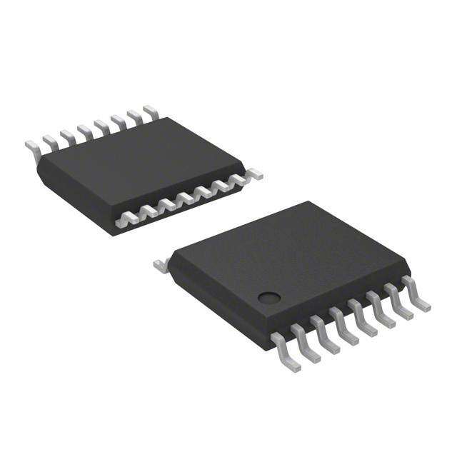
| 描述 | IC CTLR TOUCH SENSE 20SSOP触摸屏转换器和控制器 Touch Sensing Controller |
| 产品分类 | |
| 品牌 | Microchip Technology |
| 产品手册 | |
| 产品图片 |
|
| rohs | 符合RoHS无铅 / 符合限制有害物质指令(RoHS)规范要求 |
| 产品系列 | 数据转换器IC,触摸屏转换器和控制器,Microchip Technology AR1021-I/SSmTouch™ |
| 数据手册 | http://www.microchip.com/mymicrochip/filehandler.aspx?ddocname=en544070http://www.microchip.com/mymicrochip/filehandler.aspx?ddocname=en544898http://www.microchip.com/mymicrochip/filehandler.aspx?ddocname=en555235 |
| 产品型号 | AR1021-I/SS |
| 产品种类 | 触摸屏转换器和控制器 |
| 供应商器件封装 | 20-SSOP |
| 其它名称 | AR1021ISS |
| 分辨率 | 10 bit |
| 分辨率(位) | 10 b |
| 包装 | 管件 |
| 商标 | Microchip Technology |
| 安装类型 | 表面贴装 |
| 安装风格 | SMD/SMT |
| 封装 | Tube |
| 封装/外壳 | 20-SSOP(0.209",5.30mm 宽) |
| 封装/箱体 | SSOP-20 |
| 工作温度 | - 40 C to + 85 C |
| 工厂包装数量 | 67 |
| 接口类型 | 4-Wire, 5-Wire, 8-Wire, I2C, SPI |
| 数据接口 | I²C, 串行, SPI™ |
| 数据速率 | 140 SPS |
| 数据速率/采样率(SPS,BPS) | - |
| 最大工作温度 | + 85 C |
| 最小工作温度 | - 40 C |
| 标准包装 | 67 |
| 电压-电源 | 2.5 V ~ 5 V |
| 电压基准 | - |
| 电流-电源 | 17mA |
| 电源电压 | 2.5 V to 5.25 V |
| 电源电压-最大 | 5.25 V |
| 电源电压-最小 | 2.5 V |
| 电源电流 | 17 mA |
| 类型 | Resistive Touch Controllers |
| 触摸面板接口 | 4 线,5 线,8 线 |
| 评估工具 | * |
| 输入/按键数 | 3 键 |
| 输入类型 | 3 Key |
-300dpi-lyrd.jpg)


- 商务部:美国ITC正式对集成电路等产品启动337调查
- 曝三星4nm工艺存在良率问题 高通将骁龙8 Gen1或转产台积电
- 太阳诱电将投资9.5亿元在常州建新厂生产MLCC 预计2023年完工
- 英特尔发布欧洲新工厂建设计划 深化IDM 2.0 战略
- 台积电先进制程称霸业界 有大客户加持明年业绩稳了
- 达到5530亿美元!SIA预计今年全球半导体销售额将创下新高
- 英特尔拟将自动驾驶子公司Mobileye上市 估值或超500亿美元
- 三星加码芯片和SET,合并消费电子和移动部门,撤换高东真等 CEO
- 三星电子宣布重大人事变动 还合并消费电子和移动部门
- 海关总署:前11个月进口集成电路产品价值2.52万亿元 增长14.8%


PDF Datasheet 数据手册内容提取
AR1000 Series Resistive Touch Screen Controller Data Sheet Preliminary 2009-2012 Microchip Technology Inc. DS41393B
Note the following details of the code protection feature on Microchip devices: • Microchip products meet the specification contained in their particular Microchip Data Sheet. • Microchip believes that its family of products is one of the most secure families of its kind on the market today, when used in the intended manner and under normal conditions. • There are dishonest and possibly illegal methods used to breach the code protection feature. All of these methods, to our knowledge, require using the Microchip products in a manner outside the operating specifications contained in Microchip’s Data Sheets. Most likely, the person doing so is engaged in theft of intellectual property. • Microchip is willing to work with the customer who is concerned about the integrity of their code. • Neither Microchip nor any other semiconductor manufacturer can guarantee the security of their code. Code protection does not mean that we are guaranteeing the product as “unbreakable.” Code protection is constantly evolving. We at Microchip are committed to continuously improving the code protection features of our products. Attempts to break Microchip’s code protection feature may be a violation of the Digital Millennium Copyright Act. If such acts allow unauthorized access to your software or other copyrighted work, you may have a right to sue for relief under that Act. Information contained in this publication regarding device Trademarks applications and the like is provided only for your convenience The Microchip name and logo, the Microchip logo, dsPIC, and may be superseded by updates. It is your responsibility to KEELOQ, KEELOQ logo, MPLAB, PIC, PICmicro, PICSTART, ensure that your application meets with your specifications. PIC32 logo, rfPIC and UNI/O are registered trademarks of MICROCHIP MAKES NO REPRESENTATIONS OR Microchip Technology Incorporated in the U.S.A. and other WARRANTIES OF ANY KIND WHETHER EXPRESS OR countries. IMPLIED, WRITTEN OR ORAL, STATUTORY OR OTHERWISE, RELATED TO THE INFORMATION, FilterLab, Hampshire, HI-TECH C, Linear Active Thermistor, INCLUDING BUT NOT LIMITED TO ITS CONDITION, MXDEV, MXLAB, SEEVAL and The Embedded Control QUALITY, PERFORMANCE, MERCHANTABILITY OR Solutions Company are registered trademarks of Microchip FITNESS FOR PURPOSE. Microchip disclaims all liability Technology Incorporated in the U.S.A. arising from this information and its use. Use of Microchip Analog-for-the-Digital Age, Application Maestro, chipKIT, devices in life support and/or safety applications is entirely at chipKIT logo, CodeGuard, dsPICDEM, dsPICDEM.net, the buyer’s risk, and the buyer agrees to defend, indemnify and dsPICworks, dsSPEAK, ECAN, ECONOMONITOR, hold harmless Microchip from any and all damages, claims, FanSense, HI-TIDE, In-Circuit Serial Programming, ICSP, suits, or expenses resulting from such use. No licenses are Mindi, MiWi, MPASM, MPLAB Certified logo, MPLIB, conveyed, implicitly or otherwise, under any Microchip MPLINK, mTouch, Omniscient Code Generation, PICC, intellectual property rights. PICC-18, PICDEM, PICDEM.net, PICkit, PICtail, REAL ICE, rfLAB, Select Mode, Total Endurance, TSHARC, UniWinDriver, WiperLock and ZENA are trademarks of Microchip Technology Incorporated in the U.S.A. and other countries. SQTP is a service mark of Microchip Technology Incorporated in the U.S.A. All other trademarks mentioned herein are property of their respective companies. © 2009-2012, Microchip Technology Incorporated, Printed in the U.S.A., All Rights Reserved. Printed on recycled paper. ISBN: 9781620761366 QUALITY MANAGEMENT SYSTEM Microchip received ISO/TS-16949:2009 certification for its worldwide CERTIFIED BY DNV headquarters, design and wafer fabrication facilities in Chandler and Tempe, Arizona; Gresham, Oregon and design centers in California and India. The Company’s quality system processes and procedures == ISO/TS 16949 == are for its PIC® MCUs and dsPIC® DSCs, KEELOQ® code hopping devices, Serial EEPROMs, microperipherals, nonvolatile memory and analog products. In addition, Microchip’s quality system for the design and manufacture of development systems is ISO 9001:2000 certified. Preliminary DS41393B-page 2 2009-2012 Microchip Technology Inc.
AR1000 SERIES RESISTIVE TOUCH SCREEN CONTROLLER AR1000 Series Resistive Touch Screen Controller Special Features: Touch Sensor Support: • RoHS Compliant • 4-Wire, 5-Wire and 8-Wire Analog Resistive • Power-Saving Sleep mode • Lead-to-Lead Resistance: 50-2,000typical) • Industrial Temperature Range • Layer-to-Layer Capacitance: 0-0.5 uF • Built-in Drift Compensation Algorithm • Touch Sensor Time Constant: 500 us (maximum) • 128 Bytes of User EEPROM Touch Resolution: Power Requirements: • 10-bit Resolution (maximum) • Operating Voltage: 2.5-5.0V ±5% • Standby Current: Touch Coordinate Report Rate: - 5V: 85 uA, typical; 125 uA (maximum) - 2.5V: 40 uA, typical; 60 uA (maximum) • 140 Reports Per Second (typical) with a Touch • Operating “No touch” Current: Sensor of 0.02 uF with 200 Layers - 3.0 mA (typical) • Actual Report Rate is dependent on the Touch • Operating “Touch” Current: Sensor used. - 17 mA, typical, with a touch sensor having 200 layers. Communications: - Actual current is dependent on the touch sensor used • SPI, Slave mode, p/n AR1021 • AR1011/AR1021 Brown-Out Detection (BOR) set • I2CTM, Slave mode, p/n, AR1021 to 2.2V. • UART, 9600 Baud Rate, p/n AR1011 Touch Modes: • Off, Stream, Down, Up and more. Preliminary 2009-2012 Microchip Technology Inc. DS41393B-page 3
AR1000 SERIES RESISTIVE TOUCH SCREEN CONTROLLER Table of Contents 1.0 Device Overview..........................................................................................................................................................................5 2.0 Basics of Resistive Sensors.........................................................................................................................................................7 3.0 Hardware....................................................................................................................................................................................11 4.0 I2C Communications..................................................................................................................................................................17 5.0 SPI Communications..................................................................................................................................................................21 6.0 UART Communications..............................................................................................................................................................25 7.0 Touch Reporting Protocol...........................................................................................................................................................27 8.0 Configuration Registers..............................................................................................................................................................29 9.0 Commands.................................................................................................................................................................................35 10.0 Application Notes.......................................................................................................................................................................45 11.0 Electrical Specifications..............................................................................................................................................................51 12.0 Packaging Information................................................................................................................................................................53 Appendix A: Revision History...............................................................................................................................................................63 Appendix B: Device Differences...........................................................................................................................................................64 Index....................................................................................................................................................................................................65 The Microchip Web Site.......................................................................................................................................................................67 Customer Change Notification Service................................................................................................................................................67 Customer Support................................................................................................................................................................................67 Reader Response................................................................................................................................................................................68 TO OUR VALUED CUSTOMERS It is our intention to provide our valued customers with the best documentation possible to ensure successful use of your Microchip products. To this end, we will continue to improve our publications to better suit your needs. Our publications will be refined and enhanced as new volumes and updates are introduced. If you have any questions or comments regarding this publication, please contact the Marketing Communications Department via E-mail at docerrors@microchip.com or fax the Reader Response Form in the back of this data sheet to (480) 792-4150. We welcome your feedback. Most Current Data Sheet To obtain the most up-to-date version of this data sheet, please register at our Worldwide Web site at: http://www.microchip.com You can determine the version of a data sheet by examining its literature number found on the bottom outside corner of any page. The last character of the literature number is the version number, (e.g., DS30000A is version A of document DS30000). Errata An errata sheet, describing minor operational differences from the data sheet and recommended workarounds, may exist for current devices. As device/documentation issues become known to us, we will publish an errata sheet. The errata will specify the revision of silicon and revision of document to which it applies. To determine if an errata sheet exists for a particular device, please check with one of the following: • Microchip’s Worldwide Web site; http://www.microchip.com • Your local Microchip sales office (see last page) When contacting a sales office, please specify which device, revision of silicon and data sheet (include literature number) you are using. Customer Notification System Register on our web site at www.microchip.com to receive the most current information on all of our products. Preliminary DS41393B-page 4 2009-2012 Microchip Technology Inc.
AR1000 SERIES RESISTIVE TOUCH SCREEN CONTROLLER 1.0 DEVICE OVERVIEW 1.1 Applications The Microchip mTouchTM AR1000 Series Resistive The AR1000 Series is designed for high volume, small Touch Screen Controller is a complete, easy to form factor touch solutions with quick time to market integrate, cost-effective and universal touch screen requirements – including, but not limited to: controller chip. • Mobile communication devices The AR1000 Series has sophisticated proprietary • Personal Digital Assistants (PDA) touch screen decoding algorithms to process all touch • Global Positioning Systems (GPS) data, saving the host from the processing overhead. • Touch Screen Monitors Providing filtering capabilities beyond that of other • KIOSK low-cost devices, the AR1000 delivers reliable, vali- • Media Players dated, and calibrated touch coordinates. • Portable Instruments • Point of Sale Terminals Using the on-board EEPROM, the AR1000 can store and independently apply the calibration to the touch coordinates before sending them to the host. This unique combination of features makes the AR1000 the most resource-efficient touch screen controller for system designs, including embedded system integrations. FIGURE 1-1: BLOCK DIAGRAM FIGURE 1-2: PIN DIAGRAM AR1000 Series (SSOP, SOIC) AR1000 Series (QFN) 09876 21111 1 VDD VSS 20 Y-M1DD SSX- 2 M1 X- 19 S VV 3 SY- X+ 18 1 M2 X+ 15 4 M2 5WSX- 17 2 WAKE 5WSX- 14 5 WAKE Y- 16 3 SIQ Y- 13 6 SIQ Y+ 15 X X 7 SY+ SX+ 14 45 SSYS+ L/T A/R SYX++1112 8 SS SDI/SDA/RX 13 C D 190 SNDCO SCK/SCL/NTCX 1112 DOCCK/SCDI/S SNSNS 0 67891 Preliminary 2009-2012 Microchip Technology Inc. DS41393B-page 5
AR1000 SERIES RESISTIVE TOUCH SCREEN CONTROLLER TABLE 1-1: PIN DESCRIPTIONS Pin Function Description/Comments SSOP, SOIC QFN 1 18 VDD Supply Voltage 2 19 M1 Communication Selection 3 20 SY- Sense Y- (8-wire). Tie to VSS, if not used. 4 1 M2 4/8-wire or 5-wire Sensor Selection 5 2 WAKE Touch Wake-up/Touch Detection 6 3 SIQ LED Drive/SPI Interrupt. No connect, if not used. 7 4 SY+ Sense Y+ (8-wire). Tie to VSS, if not used. 8 5 SS Slave Select (SPI). Tie to VSS, if not used. 9 6 SDO SPI Serial Data Output/I2C™ Interrupt. Tie to Vss, if UART. 10 7 NC No connection. No connect or tie to VSS or VDD. 11 8 SCK/SCL/TX SPI/I2C™ Serial Clock/UART Transmit 12 9 NC No connection. No connect or tie to VSS or VDD. 13 10 SDI/SDA/RX I2C™ Serial Data/SPI Serial Data Input/UART Receive 14 11 SX+ Sense X+ (8-wire). Tie to VSS, if not used. 15 12 Y+ Y+ Drive 16 13 Y- Y- Drive 17 14 5WSX- 5W Sense (5-wire)/Sense X- (8-wire). Tie to VSS, if not used. 18 15 X+ X+ Drive 19 16 X- X- Drive 20 17 VSS Supply Voltage Ground Preliminary DS41393B-page 6 2009-2012 Microchip Technology Inc.
AR1000 SERIES RESISTIVE TOUCH SCREEN CONTROLLER 2.0 BASICS OF RESISTIVE Bus Bars or Silver Frit electrically connect the ITO on SENSORS the flex and stable layers to the sensor’s interface tail. Bus bars are typically screen printed silver ink. They are typically much lower in resistivity than the ITO. 2.1 Terminology X-Axis is the left and right direction on the touch sensor. ITO (Indium Tin Oxide) is the resistive coating that Y-Axis is the top and bottom direction on the touch makes up the active area of the touch sensor. ITO is a sensor. transparent semiconductor that is sputtered onto the touch sensor layers. Drive Lines supply a voltage gradient across the sensor. Flex or Film or Topsheet is the top sensor layer that a user touches. Flex refers to the fact that the top layer 2.2 General physically flexes from the pressure of a touch. Stable or Glass is the bottom sensor layer that Resistive 4, 5, and 8-wire touch sensors consist of two interfaces against the display. facing conductive layers, held in physical separation from each other. The force of a touch causes the top Spacer Adhesive is a frame of adhesive that connects layer to deflect and make electrical contact with the the flex and stable layers together around the perimeter bottom layer. of the sensor. Touch position measurements are made by applying a Spacer Dots maintain physical and electrical voltage gradient across a layer or axis of the touch separation between the flex and stable layers. The dots sensor. The touch position voltage for the axis can be are typically printed onto the stable layer. measured using the opposing layer. A comparison of typical sensor constructions is shown below in Table2-1. TABLE 2-1: SENSOR COMPARISON Sensor Comments 4-Wire Less expensive than 5-wire or 8-wire Lower power than 5-wire More linear (without correction) than 5-wire Touch inaccuracies occur from flex layer damage or resistance changes 5-Wire Maintains touch accuracy with flex layer damage Inherent nonlinearity often requires touch data correction Touch inaccuracies occur from resistance changes 8-Wire More expensive than 4-wire Lower power than 5-wire More linear (without correction) than 5-wire Touch inaccuracies occur from flex layer damaged Maintains touch accuracy with resistance changes The AR1000 Series Resistive Touch Screen Controllers will work with any manufacturers of analog resistive 4, 5 and 8-wire touch screens. The communications and decoding are included, allowing the user the quickest simplest method of interfacing analog resistive touch screens into their applications. The AR1000 Series was designed with an understanding of the materials and processes that make up resistive touch screens. The AR1000 Series Touch Controller is not only reliable, but can enhance the reliability and longevity of the resistive touch screen, due to its advanced filtering algorithms and wide range of operation. Preliminary 2009-2012 Microchip Technology Inc. DS41393B-page 7
AR1000 SERIES RESISTIVE TOUCH SCREEN CONTROLLER 2.3 4-Wire Sensor A 4-wire resistive touch sensor consists of a stable and flex layer, electrically separated by spacer dots. The layers are assembled perpendicular to each other. The touch position is determined by first applying a voltage gradient across the flex layer and using the stable layer to measure the flex layer’s touch position voltage. The second step is applying a voltage gradient across the stable layer and using the flex layer to measure the stable layer’s touch position voltage. The measured voltage at any position across a driven axis is predictable. A touch moving in the direction of the driven axis will yield a linearly changing voltage. A touch moving perpendicular to the driven axis will yield a relatively unchanging voltage (See Figure2-1). FIGURE 2-1: 4-WIRE DECODING Preliminary DS41393B-page 8 2009-2012 Microchip Technology Inc.
AR1000 SERIES RESISTIVE TOUCH SCREEN CONTROLLER 2.4 8-Wire Sensor The basic decoding of an 8-wire sensor is similar to a 4-wire. The difference is that an 8-wire sensor has four An 8-wire resistive touch sensor consists of a stable additional interconnects used to reference sensor and flex layer, electrically separated by spacer dots. voltage back to the controller. The layers are assembled perpendicular to each other. A touch system may experience voltage losses due to The touch position is determined by first applying a resistance changes in the bus bars and connection voltage gradient across the flex layer and using the between the controller and sensor. The losses can vary stable layer to measure the flex layer’s touch position with product use, temperature, and humidity. In a voltage. The second step is applying a voltage gradient 4-wire sensor, variations in the losses manifest them- across the stable layer and using the flex layer to selves as error or drift in the reported touch location. measure the stable layer’s touch position voltage. The four additional sense lines found on 8-wire sensors The measured voltage at any position across a driven are added to dynamically reference the voltage to cor- axis is predictable. A touch moving in the direction of rect for this fluctuation during use (See Figure2-2). the driven axis will yield a linearly changing voltage. A touch moving perpendicular to the driven axis will yield a relatively unchanging voltage. FIGURE 2-2: 8-WIRE DECODING Preliminary 2009-2012 Microchip Technology Inc. DS41393B-page 9
AR1000 SERIES RESISTIVE TOUCH SCREEN CONTROLLER 2.5 5-Wire Sensor To measure the X-axis, the left edge of the layer is driven with 0V (ground), using connections to the upper A 5-wire resistive touch sensor consists of a flex and left and lower left sensor corners. The right edge is stable layer, electrically separated by spacer dots. The driven with +5 VDC, using connections to the upper touch position is determined by first applying a voltage right and lower right sensor corners. gradient across the stable layer in the X-axis direction To measure the Y-axis, the top edge of the layer is and using the flex layer to measure the axis touch posi- driven with 0V (ground), using connections to the upper tion voltage. The second step is applying a voltage gra- left and upper right sensor corners. The bottom edge is dient across the stable layer in the Y-axis direction and using the flex layer to measure the axis touch position driven with +5 VDC, using connections to the lower left and lower right sensor corners. voltage. The measured voltage at any position across a driven The voltage is not directly applied to the edges of the axis is predictable. A touch moving in the direction of active layer, as it is for 4-wire and 8-wire sensors. The the driven axis will yield a linearly changing voltage. A voltage is applied to the corners of a 5-wire sensor. touch moving perpendicular to the driven axis will yield a relatively unchanging voltage (See Figure2-3). FIGURE 2-3: 5-Wire Decoding Preliminary DS41393B-page 10 2009-2012 Microchip Technology Inc.
AR1000 SERIES RESISTIVE TOUCH SCREEN CONTROLLER 3.0 HARDWARE 3.1 Main Schematic A main application schematic for the SOIC/SSOP package pinout is shown in Figure3-1. See Figure1-2 for the QFN package pinout. FIGURE 3-1: MAIN SCHEMATIC (SOIC/SSOP PACKAGE PINOUT) Preliminary 2009-2012 Microchip Technology Inc. DS41393B-page 11
AR1000 SERIES RESISTIVE TOUCH SCREEN CONTROLLER 3.2 4, 5, 8-Wire Sensor Selection 3.3 4-Wire Touch Sensor Interface The desired sensor type of 4/8-wire or 5-wire is Sensor tail pinouts can vary by manufacturer and part hardware selectable using pin M2. number. Ensure that both sensor tail pins for one sensor axis (layer) are connected to the controller’s X-/X+ pins and the tail pins for the other sensor axis TABLE 3-1: 4/8-WIRE vs. 5-WIRE (layer) are connected to the controller’s Y-/Y+ pins. The SELECTION controller’s X-/X+ and Y-/Y+ pin pairs do not need to Type M2 pin connect to a specific sensor axis. The orientation of controller pins X- and X+ to the two sides of a given 4/8-wire VSS sensor axis is not important. Likewise, the orientation of 5-wire VDD controller pins Y- and Y+ to the two sides of the other sensor axis is not important. If 4/8-wire has been hardware-selected, then the choice of 4-wire or 8-wire is software-selectable via the Connections to a 4-wire touch sensor are as follows TouchOptions Configuration register. (See Figure3-2). When 4/8-wire is hardware-selected, the controller defaults to 4-wire operation. If 8-wire operation is desired, then the TouchOptions Configuration register must be changed. FIGURE 3-2: 4-WIRE TOUCH SENSOR INTERFACE Tie unused controller pins 5WSX-, SX+, SY-, and SY+ to VSS. See Section3.8 “ESD Considerations” and Section3.9 “Noise Considerations” for important information regarding the capacitance of the controller schematic hardware. Preliminary DS41393B-page 12 2009-2012 Microchip Technology Inc.
AR1000 SERIES RESISTIVE TOUCH SCREEN CONTROLLER 3.4 5-Wire Touch Sensor Interface Sensor tail pinouts can vary by manufacturer and part number. Ensure sensor tail pins for one pair of diagonally related sensor corners are connected to the controller’s X-/X+ pins and the tail pins for the other pair of diagonally related corners are connected to the controller’s Y-/Y+ pins. The controller’s X-/X+ and Y-/Y+ pin pairs do not need to connect to a specific sensor axis. The orientation of controller pins X- and X+ to the two selected diagonal sensor corners is not important. Likewise, the orientation of controller pins Y- and Y+ to the other two selected diagonal sensor corners is not important. The sensor tail pin connected to its top layer must be connected to the controller’s 5WSX- pin. Connections to a 5-wire touch sensor are shown in Figure3-3 below. FIGURE 3-3: 5-WIRE TOUCH SENSOR INTERFACE Tie unused controller pins SX+, SY-, and SY+ to VSS. See “Section3.8 “ESD Considerations” and Section3.9 “Noise Considerations” for important information regarding the capacitance of the controller schematic hardware. Preliminary 2009-2012 Microchip Technology Inc. DS41393B-page 13
AR1000 SERIES RESISTIVE TOUCH SCREEN CONTROLLER 3.5 8-Wire Touch Sensor Interface Consult with the sensor manufacturer’s specification to determine which member of each edge connected pair Sensor tail pinouts can vary by manufacturer and part is the special 8-wire “sense” connection. Incorrectly number. Ensure both sensor tail pins for one sensor connecting the sense and excite lines to the controller axis (layer) are connected to the controller’s X-/X+ pins will adversely affect performance. and the tail pins for the other sensor axis (layer) are The controller requires that the main and “sense” tail connected to the controller’s Y-/Y+ pins. pin pairs for sensor edges be connected to controller The controller’s X-/X+ and Y-/Y+ pin pairs do not need pin pairs as follows: to connect to a specific sensor axis. The orientation of • Y- and SY- controller pins X- and X+ to the two sides of a given • Y+ and SY+ sensor axis is not important. Likewise, the orientation of • X- and 5WSX- controller pins Y- and Y+ to the two sides of the other • X+ and SX+ sensor axis is not important. Connections to a 8-wire touch sensor are shown in The 8-wire sensor differs from a 4-wire sensor in that Figure3-4 below. each edge of an 8-wire sensor has a secondary connection brought to the sensor’s tail. These secondary connections are referred to as “sense” lines. The controller pins associated with the sense line for an 8-wire sensor contain an ‘S’ prefix in their respective names. For example, the SY- pin is the sense line connection associated with the main Y- pin connection. FIGURE 3-4: 8-WIRE TOUCH SENSOR INTERFACE See Section3.8 “ESD Considerations” and Section3.9 “Noise Considerations” for important information regarding the capacitance of the controller schematic hardware. Preliminary DS41393B-page 14 2009-2012 Microchip Technology Inc.
AR1000 SERIES RESISTIVE TOUCH SCREEN CONTROLLER 3.6 Status LED 3.8 ESD Considerations The LED and associated resistor are optional. ESD protection is shown on the 4-wire, 5-wire, and 8-wire interface applications schematics. FIGURE 3-5: The capacitance of alternate ESD diodes may adversely affect touch performance. A lower capacitance is better. The PESD5V0S1BA parts shown in the reference design have a typical capacitance of 35 pF. Test to ensure that selected ESD protection does not degrade touch performance. ESD protection is shown in the reference design, but acceptable protection is dependent on your specific The LED serves as a status indicator that the controller application. Ensure your ESD solution meets your is functioning. It will slow flash when the controller is design requirements. running with no touch in progress. It will flicker quickly (mid-level on) when a touch is in progress. 3.9 Noise Considerations If the LED is used with SPI communication, then the LED will be off with no touch and flicker quickly Touch sensor filtering capacitors are included in the (mid-level on) when a touch is in progress. reference design. Note: If the SIQ pin is not used, it must be left as a No Connect and NOT tied to circuit VDD or Warning: Changing the value of the capacitors may VSS. adversely affect performance of the touch system. 3.7 WAKE Pin The AR1000’s WAKE pin is described as “Touch Wake-Up/Touch Detection”. It serves the following three roles in the controller’s functionality: • Wake-up from touch • Touch detection • Measure sensor capacitance The application circuit shows a 20 KΩ resistor connected between the WAKE pin and the X- pin on the controller chip. The resistor is required for product operation, based on all three of the above roles. Preliminary 2009-2012 Microchip Technology Inc. DS41393B-page 15
AR1000 SERIES RESISTIVE TOUCH SCREEN CONTROLLER NOTES: Preliminary DS41393B-page 16 2009-2012 Microchip Technology Inc.
AR1000 SERIES RESISTIVE TOUCH SCREEN CONTROLLER 4.0 I2CTM COMMUNICATIONS The AR1021 is an I2C slave device with a 7-bit address of 0x4D, supporting up to 400 kHz bit rate. A master (host) device interfaces with the AR1021. 4.1 I2C Hardware Interface A summary of the hardware interface pins is shown below in Table4-1. TABLE 4-1: I2C HARDWARE INTERFACE AR1021 Pin Description M1 Connect to VSS to select I2C™ communications SCL Serial Clock to master I2C SDA Serial Data to master I2C SDO Data ready interrupt output to master M1 Pin • The M1 pin must be connected to VSS to config- ure the AR1021 for I2C communications. SCL Pin • The SCL (Serial Clock) pin is electrically open-drain and requires a pull-up resistor, typi- cally 2.2 K to 10 K, from SCL to VDD. • SCL Idle state is high. SDA Pin • The SDA (Serial Data) pin is electrically open-drain and requires a pull-up resistor, typi- cally 2.2K to 10K, from SDA to VDD. • SDA Idle state is high. • Master write data is latched in on SCL rising edges. • Master read data is latched out on SCL falling edges to ensure it is valid during the subsequent SCL high time. SDO Pin • The SDO pin is a driven output interrupt to the master. • SDO Idle state is low. • SDO will be asserted high when the AR1021 has data ready (touch report or command response) for the master to read. Preliminary 2009-2012 Microchip Technology Inc. DS41393B-page 17
AR1000 SERIES RESISTIVE TOUCH SCREEN CONTROLLER 4.2 I2C Pin Voltage Level Characteristics TABLE 4-2: I2C PIN VOLTAGE LEVEL CHARACTERISTICS Function Pin Input Output SCL/SCK SCL/SCK/TX VSS ≤ VIL≤ 0.2*VDD — 0.8*VDD ≤ VIH ≤ VDD SDO SDO — VSS ≤ VOL(1) ≤ (1.2V – 0.15*VDD)(2) (1.25*VDD – 2.25V)(3) ≤ VOH(1) ≤ VDD SDA SDI/SDA/RX VSS ≤ VIL ≤ 0.2*VDD Open-drain 0.8*VDD ≤ VIH ≤ VDD Note 1: These parameters are characterized but not tested. 2: At 10 mA. 3: At –4 mA. 4.3 Addressing The AR1021’s device ID 7-bit address is: 0x4D TABLE 4-5: I2C DEVICE READ ID (0b1001101) ADDRESS A7 A6 A5 A4 A3 A2 A1 A0 TABLE 4-3: I2C DEVICE ID ADDRESS 1 0 0 1 1 0 1 1 0x9B Device ID Address, 7-bit 4.4 Master Read Bit Timing A7 A6 A5 A4 A3 A2 A1 Master read is to receive touch reports and command 1 0 0 1 1 0 1 responses from the AR1021. • Address bits are latched into the AR1021 on the TABLE 4-4: I2C DEVICE WRITE ID rising edges of SCL. ADDRESS • Data bits are latched out of the AR1021 on the rising edges of SCL. A7 A6 A5 A4 A3 A2 A1 A0 • ACK is presented (by AR1021 for address, by 1 0 0 1 1 0 1 0 0x9A master for data) on the ninth clock. • The master must monitor the SCL pin prior to asserting another clock pulse, as the AR1021 may be holding off the master by stretching the clock. FIGURE 4-1: I2C MASTER READ BIT TIMING DIAGRAM Steps 4. AR1021 compares the received address to its device ID. If they match, the AR1021 1. SCL and SDA lines are Idle high. acknowledges (ACK) the master sent address 2. Master presents “Start” bit to the AR1021 by by presenting a low on SDA, followed by a taking SDA high-to-low, followed by taking SCL low-high-low on SCL. high-to-low. 5. Master monitors SCL, as the AR1021 may be 3. Master presents 7-bit Address, followed by a “clock stretching”, holding SCL low to indicate R/W = 1 (Read mode) bit to the AR1021 on that the master should wait. SDA, at the rising edge of eight master clock (SCL) cycles. Preliminary DS41393B-page 18 2009-2012 Microchip Technology Inc.
AR1000 SERIES RESISTIVE TOUCH SCREEN CONTROLLER 6. Master receives eight data bits (MSb first) 9. Master presents a “Stop” bit to the AR1021 by presented on SDA by the AR1021, at eight taking SCL low-high, followed by taking SDA sequential master clock (SCL) cycles. The data low-to-high. is latched out on SCL falling edges to ensure it is valid during the subsequent SCL high time. 4.5 Master Write Bit Timing 7. If data transfer is not complete, then: Master write is to send supported commands to the - Master acknowledges (ACK) reception of the AR1021. eight data bits by presenting a low on SDA, followed by a low-high-low on SCL. • Address bits are latched into the AR1021 on the - Go to step 5. rising edges of SCL. • Data bits are latched into the AR1021 on the 8. If data transfer is complete, then: rising edges of SCL. - Master acknowledges (ACK) reception of the • ACK is presented by AR1021 on the ninth clock. eight data bits and a completed data transfer • The master must monitor the SCL pin prior to by presenting a high on SDA, followed by a asserting another clock pulse, as the AR1021 low-high-low on SCL. may be holding off the master by stretching the clock. FIGURE 4-2: I2C MASTER WRITE BIT TIMING DIAGRAM Steps 4.6 Clock Stretching 1. SCL and SDA lines are Idle high. The master normally controls the clock line SCL. Clock 2. Master presents “Start” bit to the AR1021 by stretching is when the slave device holds the SCL line taking SDA high-to-low, followed by taking SCL low, indicating to the master that it is not ready to high-to-low. continue the communications. 3. Master presents 7-bit Address, followed by a During communications, the AR1021 may hold off the R/W = 0 (Write mode) bit to the AR1021 on master by stretching the clock with a low on SCL. SDA, at the rising edge of eight master clock (SCL) cycles. The master must monitor the slave SCL pin to ensure the AR1021 is not holding it low, prior to asserting 4. AR1021 compares the received address to its another clock pulse for transmitting or receiving. device ID. If they match, the AR1021 acknowledges (ACK) the master sent address 4.7 AR1020 Write Conditions by presenting a low on SDA, followed by a low-high-low on SCL. The AR1020 part does not implement clock stretching 5. Master monitors SCL, as the AR1021 may be on write conditions. “clock stretching”, holding SCL low to indicate A 50 us delay is needed before the Stop bit, when the master should wait. clocking a command to the AR1020. 6. Master presents eight data bits (MSb first) to the AR1021 on SDA, at the rising edge of eight mas- ter clock (SCL) cycles. 7. AR1021 acknowledges (ACK) receipt of the eight data bits by presenting a low on SDA, fol- lowed by a low-high-low on SCL. 8. If data transfer is not complete, then go to step 5. 9. Master presents a “Stop” bit to the AR1021 by taking SCL low-high, followed by taking SDA low-to-high. Preliminary 2009-2012 Microchip Technology Inc. DS41393B-page 19
AR1000 SERIES RESISTIVE TOUCH SCREEN CONTROLLER 4.8 Touch Report Protocol Touch coordinates, when available, are provided to the master by the AR1021 in the following protocol (See Figure4-3). FIGURE 4-3: I2C TOUCH REPORT PROTOCOL Note that the IRQ signal shown above occurs on the SDO pin of the AR1021. 4.9 Command Protocol The master issues supported commands to the AR1021 in the following protocol. Below is an example of the ENABLE_TOUCH command (see Figure4-4). FIGURE 4-4: I2C COMMAND PROTOCOL Note that the IRQ shown above occurs on the SDO pin. 4.10 Sleep State • 0x9A AR1021 Device ID address Pending communications are not maintained through a • 0x00 Protocol command byte (send 0x00 for sleep/wake cycle. the protocol command register) • 0x55 Header If the SDO pin is asserted for a pending touch report or • 0x01 Data size command response, and the AR1021 enters a Sleep • 0x12 Command state, prior to the master performing a read on the data, then the data is lost. Preliminary DS41393B-page 20 2009-2012 Microchip Technology Inc.
AR1000 SERIES RESISTIVE TOUCH SCREEN CONTROLLER 5.0 SPI COMMUNICATIONS SPI operates in Slave mode with an Idle low SCK and data transmitted on the SCK falling edge. 5.1 SPI Hardware Interface A summary of the hardware interface pins is shown below in Table5-1. TABLE 5-1: SPI HARDWARE INTERFACE AR1021 Pin Description M1 Connect to VDD to select SPI communications SDI Serial data sent from master SCK Serial clock to master SDO Serial data to master SPI SIQ Interrupt output to master (optional) SS Slave Select (optional) SCK Pin SIQ Pin • The AR1021 controller’s SCL/SCK/TX pin • The AR1021 controller’s SIQ pin provides an receives Serial Clock (SCK), controlled by the optional interrupt output from the controller to the host. host. • The Idle state of the SCK should be low. • The SIQ pin is asserted high when the controller • Data is transmitted on the falling edge of SCK. has data available (a touch report or a command response) for the host. SDI Pin • The SIQ pin is deasserted after the host clocks • The AR1021 controller’s SDI/SDA/RX pin reads out the first byte of the data packet. Serial Data Input (SDI), sent by the host. SDO Pin Note: The AR1000 Development kit PICkit™ • The AR1021 controller’s SDO pin presents Serial Serial Pin 1 is designated for the SIQ Data Output (SDO) to the host. interrupt pin after the firmware updated is executed for the PICkit. SS Pin • The AR1021 controller’s SS pin provides optional “slave select” functionality. SS Pin Level AR1021 Select VSS Active VDD Inactive In the ‘inactive’ state, the controller’s SDO pin presents a high-impedance in order to prevent bus contention with another device on the SPI bus. Preliminary 2009-2012 Microchip Technology Inc. DS41393B-page 21
AR1000 SERIES RESISTIVE TOUCH SCREEN CONTROLLER 5.2 SPI Pin Voltage Level Characteristics TABLE 5-2: SPI PIN VOLTAGE CHARACTERISTICS Operating Voltage: 2.5V ≤ VDD ≤ 5.25V Function Pin Input Output SCK SCL/SCK/TX VSS ≤ VIL ≤ 0.2*VDD — 0.8*VDD ≤ VIH ≤ VDD SDI SDI/SDA/RX VSS ≤ VIL ≤ 0.2*VDD — 0.8*VDD ≤ VIH ≤ VDD SDO SDO — VSS ≤ VOL(1) ≤ (1.2V – 0.15*VDD)(2) (1.25*VDD – 2.25V)(3) ≤ VOH(1) ≤ VDD SIQ SIQ — VSS ≤ VOL(1) ≤ (1.2V – 0.15*VDD)(2) (1.25*VDD – 2.25V)(3) ≤ VOH(1) ≤ VDD SS SS VSS ≤ VIL ≤ 0.2*VDD 0.8*VDD ≤ VIH ≤ VDD Note 1: These parameters are characterized but not tested. 2: At 10 mA. 3: At -4 mA. 5.3 Data Flow 5.4 Touch Report Protocol SPI data is transferred by the host clocking the AR1021 The AR1021 controller’s touch reporting is interrupt controller’s Serial Clock (SCK) pin. driven: Each host driven clock cycle simultaneously shifts a bit • The AR1021 controller asserts the SIQ interrupt of data into and out from the AR1021 controller: pin high when it has a touch report ready. • The host clocks out the bytes of the touch report • Out from the AR1021 controller’s Serial Data Out packet from the AR1021 controller. (SDO) line. • The AR1021 controller clears the SIQ interrupt pin • Into the AR1021 controller’s Serial Data In (SDI) low, after the first byte of the touch report packet line. has been clocked out by the host. The data is shifted Most Significant bit (MSb) first. The communication protocol for the AR1021 controller If the host clocks data out from the AR1021 controller reporting touches to the host as shown below in when no valid data is available, then a byte value of Figure5-1. 0x4d will be presented by the controller. FIGURE 5-1: SPI TOUCH REPORT PROTOCOL Preliminary DS41393B-page 22 2009-2012 Microchip Technology Inc.
AR1000 SERIES RESISTIVE TOUCH SCREEN CONTROLLER 5.5 Command Protocol • The host clocks out the bytes of the command response from the AR1021 controller. The AR1021 controller receives commands from the • The AR1021 controller clears the SIQ interrupt pin host as follows: low, after the first byte of the command response • The host clocks the bytes of a command to the has been clocked out by the host. AR1021 controller. The communication protocol for the host sending the • The AR1021 controller asserts the SIQ interrupt ENABLE_TOUCH command to the AR1021 controller is pin high when it is ready with a response to the shown below in Figure5-2. command sent by the host. FIGURE 5-2: SPI TIMING DIAGRAM – COMMAND PROTOCOL (ENABLE_TOUCH) 5.6 SPI Bit Timing – General General timing waveforms are shown below in Figure5-3. FIGURE 5-3: SPI GENERAL BIT TIMING WAVEFORM Preliminary 2009-2012 Microchip Technology Inc. DS41393B-page 23
AR1000 SERIES RESISTIVE TOUCH SCREEN CONTROLLER 5.7 Timing – Bit Details 5.7.2 INTER-BYTE DELAY The AR1021 controller requires an inter-byte delay of 5.7.1 BIT RATE ~50 us. This means the host should wait ~50 us The SPI standard does not specify a maximum data between the end of clocking a given byte and the start rate for the serial bus. In general, SPI data rates can be of clocking the next byte. in MHz. Peripherals devices, such as the AR1021 controller, specify their own unique maximum SPI data 5.7.3 BIT TIMING – DETAIL rates. Characterized timing details are shown below, in The maximum SPI bit rate for the AR1021 controller is Figure5-4. ~900 kHz. Characterization has been performed at bit rates of ~39 kHz and ~156 kHz. FIGURE 5-4: SPI BIT TIMING – DETAIL TABLE 5-3: SPI BIT TIMING MIN. AND MAX. VALUES Parameter Number(1) Parameter Description Min. Max. Units 10 SS↓ (select) to SCK↑ (initial) 500 — ns 11 SCK high 550 — ns 12 SCK low 550 — ns 13 SCK↓ (last) to SS↑ (deselect) 800 — ns 14 SDI setup before SCK↓ 100 — ns 15 SDI hold after SCK↓ 100 — ns 16 SDO valid after SCK↓ — 150 ns 17 SDO↑ rise — 50 ns 18 SDO↓ fall — 50 ns 19 SS↑ (deselect) to SDO High-z 10 50 ns Note 1: Parameters are characterized, but not tested. Preliminary DS41393B-page 24 2009-2012 Microchip Technology Inc.
AR1000 SERIES RESISTIVE TOUCH SCREEN CONTROLLER 6.0 UART COMMUNICATIONS TABLE 6-1: UART HARDWARE INTERFACE AR1011 Pin Description M1 Connect M1 to VDD to select UART communications TX Transmit to host RX Receive from host SDO Connect SDO to VSS UART communication is fixed at 9600 baud rate, 8N1 format. Sleep mode will cause the TX line to drop low, which may appear as a 0x00 byte sent from the controller. Preliminary 2009-2012 Microchip Technology Inc. DS41393B-page 25
AR1000 SERIES RESISTIVE TOUCH SCREEN CONTROLLER NOTES: Preliminary DS41393B-page 26 2009-2012 Microchip Technology Inc.
AR1000 SERIES RESISTIVE TOUCH SCREEN CONTROLLER 7.0 TOUCH REPORTING PROTOCOL Touch coordinates are sent from the controller to the host system in a 5-byte data packet, which contains the X-axis coordinate, Y-axis coordinate, and a “Pen-Up/ Down” touch status. The range for X-axis and Y-axis coordinates is from 0- 4095 (12-bit). The realized resolution is 1024, and bits X1:X0 and Y1:Y0 are zeros. It is recommended that applications be developed to read the 12-bit coordinates from the packet and use them in a 12-bit format. This enhances the application robustness, as it will work with either 10 or 12 bits of coordinate information. The touch coordinate reporting protocol is shown below in Table7-1. TABLE 7-1: TOUCH COORDINATE REPORTING PROTOCOL Byte # Bit 7 Bit 6 Bit 5 Bit 4 Bit 3 Bit 2 Bit 1 Bit 0 1 1 R R R R R R P 2 0 X6 X65 X4 X3 X2 X1 X0 3 0 0 0 X11 X10 X9 X8 X7 4 0 Y6 Y5 Y4 Y3 Y2 Y1 Y0 5 0 0 0 Y11 Y10 Y9 Y8 Y7 where: • P: 0 Pen Up, 1 Pen Down • R: Reserved • X11-X0: X-axis coordinate • Y11-Y0: Y-axis coordinate Preliminary 2009-2012 Microchip Technology Inc. DS41393B-page 27
AR1000 SERIES RESISTIVE TOUCH SCREEN CONTROLLER NOTES: Preliminary DS41393B-page 28 2009-2012 Microchip Technology Inc.
AR1000 SERIES RESISTIVE TOUCH SCREEN CONTROLLER 8.0 CONFIGURATION REGISTERS 8.1 Restoring Default Parameters The Configuration registers allow application specific • AR1010/AR1020 customization of the controller. The default values have The factory default settings for the Configuration been optimized for most applications and are registers can be recovered by writing a value of 0xFF automatically used, unless you choose to change to address 0x00 of the EEPROM, then cycling power. them. • AR1011/AR1021 Unique sensors and/or product applications may The factory default settings for the Configuration benefit from adjustment of Configuration registers. registers can be recovered by writing a value of 0xFF to addresses 0x01 and 0x29 of the EEPROM, then cycling power. Note: Although most registers can be configured for a value ranging from 0 to 255, using a value outside the specified range for the specific register may negatively impact performance. TABLE 8-1: CONFIGURATION REGISTERS AR1010/ AR1011/ Address Register Name Bit 7 Bit 6 Bit 5 Bit 4 Bit 3 Bit 2 Bit 1 Bit 0 AR1020 AR1021 Offset Default Default <Special Use> 0x00 <Non-Configurable> 0x58 0x58 <Special Use> 0x01 <Non-Configurable> 0x01 0x01 TouchThreshold 0x02 Value of: 0-255 0xC5 0xC5 SensitivityFilter 0x03 Value of: 0-255 0x04 0x04 SamplingFast 0x04 Value of: 1, 2, 4, 8, 16, 32, 64, 128 0x04 0x04 SamplingSlow 0x05 Value of: 1, 2, 4, 8, 16, 32, 64, 128 0x10 0x10 AccuracyFilterFast 0x06 Value of: 1-8 0x02 0x04 AccuracyFilterSlow 0x07 Value of: 1-8 0x08 0x08 SpeedThreshold 0x08 Value of: 0-255 0x04 0x04 <Special Use> 0x09 <Non-Configurable> 0x23 0x23 SleepDelay 0x0A Value of: 0-255 0x64 0x64 PenUpDelay 0x0B Value of: 0-255 0x80 0x80 TouchMode 0x0C PD2 PD1 PD0 PM1 PM0 PU2 PU1 PU0 0xB1 0xB1 TouchOptions 0x0D — — — — — — 48W CCE 0x00 0x00 CalibrationInset 0x0E 0x19 0x19 PenStateReportDelay 0x0F Value of: 0-40 0xC8 0xC8 <Special Use> 0x10 Value of: 0-255 0x03 0x03 TouchReportDelay 0x11 <Non-Configurable> 0x00 0x00 <Special Use> 0x12 Value of: 0-255 0x00 0x00 Configuration registers are defined as an Offset value • Issue the REGISTER_READ or REGISTER_WRITE from the Start address for the register group. command, using the calculated register’s absolute address. To read or write to a register, do the following: • Issue the REGISTER_START_ADDRESS_REQUEST com- Warning: Use of invalid register values will yield mand to obtain the Start address for the register unpredictable results. group. • Calculate the desired register’s absolute address by adding the register’s Offset value to Start address for the register group. Preliminary 2009-2012 Microchip Technology Inc. DS41393B-page 29
AR1000 SERIES RESISTIVE TOUCH SCREEN CONTROLLER 8.2 Register Descriptions 8.2.5 AccuracyFilterFast Register (OFFSET 0x06) 8.2.1 TouchThreshold Register (OFFSET The AccuracyFilterFast register sets the level of an 0x02) accuracy enhancement filter, used when the touch The TouchThreshold register sets the threshold for a movement is fast. See the SpeedThreshold register for touch condition to be detected as a touch. A touch is information on the touch movement threshold. A lower detected if it is below the TouchThreshold setting. Too value will provide better touch coordinate resolution small of a value might prevent the controller from when the touch motion is fast, but may exhibit more accepting a real touch, while too large of a value might low-frequency noise error in the touch position. A allow the controller to accept very light or false touch higher value will reduce touch coordinate resolution conditions. Valid values are as follows: when the touch motion is fast, but will reduce low-fre- quency random noise error in the touch position. Valid 0 ≤ TouchThreshold ≤ 255 values are as follows: 8.2.2 SensitivityFilter Register (OFFSET 1 ≤ AccuracyFilterFast ≤ 8 0x03) Higher values may improve accuracy with some The SensitivityFilter register sets the level of touch sen- sensors. sitivity. A higher value is more sensitive to a touch (accepts a lighter touch), but may exhibit a less stable 8.2.6 AccuracyFilterSlow Register touch position. A lower value is less sensitive to a touch (OFFSET 0x07) (requires a harder touch), but will provide a more stable The AccuracyFilterSlow register sets the level of an touch position. Valid values are as follows: accuracy enhancement filter, used when the touch 0 ≤ SensitivityFilter ≤ 10 movement is slow. See the SpeedThreshold register for information on the touch movement threshold. A lower 8.2.3 SamplingFast Register (OFFSET value will provide better touch coordinate resolution 0x04) when the touch motion is slow, but may exhibit more low-frequency noise error in the touch position. A The SamplingFast register sets the level of touch mea- higher value will reduce touch coordinate resolution surement sample averaging, when touch movement is when the touch motion is slow, but will reduce low-fre- determined to be fast. See the SpeedThreshold regis- quency random noise error in the touch position. Valid ter for information on the touch movement threshold. A values are as follows: lower value will provide for a higher touch coordinate reporting rate when touch movement is fast, but may 1 ≤ AccuracyFilterSlow ≤ 8 exhibit more high-frequency random noise error in the touch position. A higher value will reduce the touch 8.2.7 SpeedThreshold Register (OFFSET coordinate reporting rate when touch movement is fast, 0x08) but will reduce high-frequency random noise error in The SpeedThreshold register sets the threshold for the touch position. Valid values are as follows: touch movement to be considered as slow or fast. A SamplingFast: <1, 4, 8, 16, 32, 64, 128> lower value reduces the touch movement speed that will be considered as fast. A higher value increases the Recommended Values: <4, 8, 16> touch movement speed that will be considered as fast. Higher values may improve accuracy with some Valid values are as follows: sensors. 0 ≤ SpeedThreshhold ≤ 255 8.2.4 SamplingSlow Register (OFFSET 0x05) The SamplingSlow register sets the level of touch mea- surement sample averaging, when touch movement is slow. See the SpeedThreshold register for information on the touch movement threshold. A lower value will increase the touch coordinate reporting rate when the touch motion is slow, but may exhibit a less stable more jittery touch position. A higher value will decrease the touch coordinate reporting rate when the touch motion is slow, but will provide a more stable touch position. Valid values are as follows: SamplingSlow: 1, 2, 4, 8, 16, 32, 64, 128 Preliminary DS41393B-page 30 2009-2012 Microchip Technology Inc.
AR1000 SERIES RESISTIVE TOUCH SCREEN CONTROLLER 8.2.8 SleepDelay Register (OFFSET 0x0A) 8.2.10 TouchMode Register (OFFSET 0x0C) The SleepDelay register sets the time duration with no The TouchMode register configures the action taken for touch or command activity that will cause the controller various touch states. to enter a low-power Sleep mode. Valid values are as There are three states of touch for the controller’s touch follows: reporting action which can be independently controlled. 0 ≤ SleepDelay ≤ 255 Touch States: Sleep Delay Time = SleepDelay * 100 ms; when Sleep- 1. Pen Down (initial touch) Delay > 0 User defined 0-3 touch reports, with selectable pen A value of zero disables the Sleep mode, such that the states. controller will never enter low-power Sleep mode. 2. Pen Movement (touch movement after initial A touch event will wake the controller from low-power touch) Sleep mode and start sending touch reports. Commu- nications sent to the controller will wake it from the low- User defined no-touch reports or streaming touch power Sleep mode and initiate action to the command. reports, with selectable pen states. 3. Pen Up (touch release) 8.2.9 PenUpDelay Register (OFFSET User defined 0-3 touch reports, with selectable pen 0x0B) states. The PenUpDelay register sets the duration of a pen-up Every touch report includes a “P” (Pen) bit that event that the controller will allow, without sending a indicates the pen state. pen-up report for the event. The delay time is started upon detecting a pen-up condition. • Pen Down: P = 1 • Pen Up: P = 0 If a pen down is reestablished before the delay time expires, then pen-down reports will continue without a pen up being sent. This effectively debounces a touch event in process. A lower value will make the controller more responsive to pen ups, but will cause more touch drop outs with a lighter touch. A higher value will make the controller less responsive to pen ups, but will reduce the number of touch drop outs with a lighter touch. Valid values are as follows: 0 ≤ PenUpDelay ≤ 255 Pen-up Delay Time ≈ PenUpDelay * 240 μs Preliminary 2009-2012 Microchip Technology Inc. DS41393B-page 31
AR1000 SERIES RESISTIVE TOUCH SCREEN CONTROLLER REGISTER 8-1: TouchMode REGISTER FORMAT R/W R/W R/W R/W R/W R/W R/W R/W PD2 PD1 PD0 PM1 PM0 PU2 PU1 PU0 bit 7 bit 0 Legend: R = Readable bit W = Writable bit U = Unimplemented bit, read as ‘0’ bit 7-5 PD<2:0>: Pen-Down State bits (action taken upon pen down). 000 = No touch report 001 = Touch report with P=0 010 = Touch report with P=1 011 = Touch report with P=1, then touch report with P=0 100 = Touch report with P=0, then touch report with P=1, then touch report with P=0 101 = Touch report with P=0, then touch report with P=1 bit 4-3 PM<1:0>: Pen Movement State bits (action taken upon pen movement). 00 = No touch report 01 = Touch report with P=0 10 = Touch report with P=1 bit 2-0 PU<2:0>: Pen-Up State bits (action taken upon pen up). 000 = No touch report 001 = Touch report with P=0 010 = Touch report with P=1 011 = Touch report with P=1, then touch report with P=0 100 = Touch report with P=0, then touch report with P=1, then touch report with P=0 101 = Touch report with P=0, then touch report with P=1 A couple of typical setup examples for the TouchMode are as follows: • Report a pen down P=1 on initial touch, followed by reporting a stream of pen downs P=1 during the touch, followed by a final pen up P=0 on touch release. TouchMode = 0b01010001 = 0x51 • Report a pen up P=0 then a pen down P=1 on initial touch, followed by reporting a stream of pen downs P=1 during the touch, followed by a final pen up P=0 on touch release. TouchMode = 0b10110001 = 0xB1 Preliminary DS41393B-page 32 2009-2012 Microchip Technology Inc.
AR1000 SERIES RESISTIVE TOUCH SCREEN CONTROLLER 8.2.11 TouchOptions Register (OFFSET 0x0D) The TouchOptions register contains various “touch” related option bits. REGISTER 8-2: TouchOptions REGISTER U-0 U-0 U-0 U-0 U-0 U-0 R/W R/W — — — — — — 48W CCE bit 7 bit 0 Legend: R = Readable bit W = Writable bit U = Unimplemented bit, read as ‘0’ bit 7-2 Unimplemented: Read as ‘0’ bit 1 48W: 4-Wire or 8-Wire Sensor Selection bit 1 = Selects 8-wire Sensor Operating mode 0 = Selects 4-wire Sensor Operating mode bit 0 CCE: Calibrated Coordinates Enable bit 1 = Enables calibrated coordinates, if the controller has been calibrated 0 = Disables calibrated coordinates Calibration Inset = (CalibrationInset/2) %, Range of 0- 20% with 0.5% resolution Note: A 4-wire touch sensor will not work if the For example, CalibrationInset = 25 (0x19) yields a cal- 48W Configuration bit is incorrectly ibration inset of (25/2) or 12.5%. During the calibration defined as 1, which selects 8-wire. procedure, the controller will internally extrapolate the An 8-wire touch sensor will provide basic calibration point touch values in Calibration mode by operation if the 48W Configuration bit is 12.5% to achieve full scale. incorrectly defined as 0, which selects 4- wire. However, the benefit of the 8-wire FIGURE 8-1: sensor will only be realized if the 48W Configuration bit is correctly defined as 1, selecting 8-wire. 12.5% of 8.2.12 CalibrationInset Register (OFFSET Full Scale 0x0E) The CalibrationInset register defines the expected 12.5% of position of the calibration points, inset from the perime- Full Scale Location of Calibration ter of the touch sensor’s active area, by a percentage Targets presented during of the full scale dimension. Calibration. This allows for the calibration targets to be placed inset from edge to make it easier for a user to touch them. The CalibrationInset register value is only used when the CALIBRATION_MODE command is issued to the controller. In Calibration mode, the controller will extrapolate the calibration point touch report values by the defined CalibrationInset percentage to achieve full scale. A software application that issues the CALIBRATION_MODE command must present the displayed calibration targets at the same inset percentage as defined in this CalibrationInset register. Valid values are as follows: 0 ≤ CalibrationInset ≤ 40 Preliminary 2009-2012 Microchip Technology Inc. DS41393B-page 33
AR1000 SERIES RESISTIVE TOUCH SCREEN CONTROLLER 8.2.13 PenStateReportDelay Register (OFFSET 0x0F) The PenStateReportDelay register sets the delay time between sending of sequential touch reports for the “Pen-Down” and “Pen-Up” Touch mode states. See Section8.2.10 “TouchMode Register (offset 0x0C)” for touch modes. For example, if “Pen-Up” state of the TouchMode register is configured to send a touch report with P=1, followed by a touch report with P=0, then this delay occurs between the two touch reports. This provides some timing flexibility between the two touch reports that may be desired in certain applications. Valid values are as follows. 0 ≤ PenStateReportDelay ≤ 255 Pen State Report Delay Time = PenStateReportDelay * 50 μs 8.2.14 TouchReportDelay Register (OFFSET 0x11) The TouchReportDelay register sets a forced delay time between successive touch report packets. This allows slowing down of the touch report rate, if desir- able for a given application. For example, a given appli- cation may not need a high rate of touch reports and may want to reduce the overhead used to service all of the touch reports being sent. In this situation, increas- ing the value of this register will reduce the rate at which the controller sends touch reports. Valid values are as follows: 0 ≤ TouchReportDelay ≤ 255 Touch Report Delay Time ≈ TouchReportDelay * 500 μs Preliminary DS41393B-page 34 2009-2012 Microchip Technology Inc.
AR1000 SERIES RESISTIVE TOUCH SCREEN CONTROLLER 9.0 COMMANDS 9.1 Sending Commands 9.1.1 COMMAND SEND FORMAT The controller supports application-specific configuration commands as shown in Table9-1, below. TABLE 9-1: COMMAND SEND FORMAT Byte # Name Value Description 1 Header 0x55 Header (mark beginning of command packet) 2 Size 0x<> Size, # of bytes following this byte 3 Command 0x<> Command ID 4 Data 0x<> Data, if applicable for the command : Data 0x<> Data, if applicable for the command To ensure command communication is not interrupted by touch activity, it is recommended that the controller touch is disabled, prior to other commands. This can be done as follows: 1. Send DISABLE_TOUCH command 2. Wait 50 ms 3. Send desired commands 4. Send ENABLE_TOUCH command 9.1.2 COMMAND RESPONSE A received command will be responded to as seen in Table9-2 below. TABLE 9-2: COMMAND RESPONSE FORMAT Byte # Name Value Description 1 Header 0x55 Header (mark beginning of command packet) 2 Size 0x<> Size, # of bytes following this byte 3 Status 0x<> Status 4 Command 0x<> Command ID 5 Data 0x<> Data, if applicable for the command : Data 0x<> Data, if applicable for the command The “Status” value within the response packet should be one of the following (See Table9-3): TABLE 9-3: COMMAND RESPONSE STATUS VALUES Status Value Description 0x00 Success 0x01 Command Unrecognized 0x03 Header Unrecognized 0x04 Command Time Out (exceeded ~100 ms) 0xFC Cancel Calibration mode Preliminary 2009-2012 Microchip Technology Inc. DS41393B-page 35
AR1000 SERIES RESISTIVE TOUCH SCREEN CONTROLLER 9.1.3 DISABLE TOUCH BEFORE SENDING SUBSEQUENT COMMANDS The AR1000 does not support full duplex communications. It cannot send touch reports to the host simultaneously with receiving commands from the host. Disable AR1000 touch reporting prior to sending any other command(s), then re-enable touch reporting when complete with executing other commands. 1. Send the DISABLE_TOUCH command. Check for expected command response. 2. Send a desired command. Check for expected command response. 3. Repeat at step 2 if another command is to be sent. 4. Send the ENABLE_TOUCH command. Check for expected command response. 9.1.4 CONFIRM COMMAND IS SENT Confirm each command sent to the AR1000, prior to issuing another command, to ensure it is executed. This is accomplished by evaluating the AR1000 response to a command that has been sent to it. Check for each of the following five conditions to be met (See Table9-4). TABLE 9-4: COMMAND RESPONSE ERROR CONDITIONS Condition Response Byte Description Header 1 Header 0x55 value is expected Size 2 Size 0x<> value to match what is expected for command sent Status 3 Status 0x00 “success” value is expected ID 4 Command ID 0x<> value to match what is expected (ID of sent command) Data 5 to end Data byte count to match what is expected for command sent 0x<> represents a value that is dependent on the com- mand. An error has occurred if no response is received at all or if any of the above conditions are not met in the response from the AR1000. If an error condition occurs, delay for a period of ~50 ms then send the same command again. Preliminary DS41393B-page 36 2009-2012 Microchip Technology Inc.
AR1000 SERIES RESISTIVE TOUCH SCREEN CONTROLLER 9.2 AR1000 Commands TABLE 9-5: COMMAND SET SUMMARY Command Command Description Value 0x10 GET_VERSION 0x12 ENABLE_TOUCH 0x13 DISABLE_TOUCH 0x14 CALIBRATE_MODE 0x20 REGISTER_READ 0x21 REGISTER_WRITE 0x22 REGISTER_START_ADDRESS_REQUEST 0x23 REGISTERS_WRITE_TO_EEPROM 0x28 EEPROM_READ 0x29 EEPROM_WRITE 0x2B EEPROM_WRITE_TO_REGISTERS 9.3 AR1000 Command Descriptions 9.3.1 GET_VERSION – 0x10 Controller will return version number and type. Send: <0x55><0x01><0x10> Receive: <0x55><0x05><Response><0x10><Ver- sion High><Version Low><Type> where <Type> REGISTER 9-1: GET_VERSION <TYPE> FORMAT R/W R/W R/W R/W R/W R/W R/W R/W RS1 RS0 TP5 TP4 TP3 TP2 TP1 TP0 bit 7 bit 0 Legend: R = Readable bit W = Writable bit U = Unimplemented bit, read as ‘0’ bit 7-6 RS<1:0>: Resolution of Touch Coordinates bits 00 = 8-bit 01 = 10-bit 10 = 12-bit bit 5-0 TP<5:0>: Type of Controller bits 001010 = ARA10 9.3.2 ENABLE_TOUCH – 0x12 9.3.3 DISABLE_TOUCH – 0x13 Controller will send touch coordinate reports for valid Controller will not send any touch coordinate reports. A touch conditions. touch will, however, still wake-up the controller if asleep. Send: <0x55><0x01><0x12> Send: <0x55><0x01><0x13> Receive: <0x55><0x02><Response><0x12> Receive: <0x55><0x02><Response><0x13> Preliminary 2009-2012 Microchip Technology Inc. DS41393B-page 37
AR1000 SERIES RESISTIVE TOUCH SCREEN CONTROLLER 9.3.4 CALIBRATE – 0x14 Enter Calibration mode. This instructs the controller to enter a mode of accepting the next four touches as the calibration point coordinates. See Section10.1 “Cali- bration of Touch Sensor with Controller” for an example. Completion of Calibration mode will automatically store the calibration point coordinates in on-board controller memory and set (to 1) the CCE bit of the TouchOptions register. This bit enables the controller to report touch coordinates that have been processed with the previously collected calibration data. To provide for proper touch orientation, the four sequential calibration touches must be input in the physical order on the touch sensor, as shown in Figure9-1. FIGURE 9-1: CALIBRATION ROUTINE SEQUENCE #1 #2 Upper Left Upper Right Touch Sensor #4 #3 Lower Left Lower Right Upon completion, the controller’s register values and calibration data are stored to the EEPROM. The Calibration mode will be cancelled by sending any command before the mode has been completed. If the calibration is canceled, the controller response may appear incorrect or incomplete. This is expected behavior. Preliminary DS41393B-page 38 2009-2012 Microchip Technology Inc.
AR1000 SERIES RESISTIVE TOUCH SCREEN CONTROLLER 9.3.4.1 AR1010/AR1020 Calibrate Response Send: <0x55><0x02><0x14><Calibration Type> Calibration Type Description 0x04 4 point Receive: <0x55><0x02><0x00><0x14> for initial command response <0x55><0x02><0x00><0x14> Response for touch of Calibration point #1 <0x55><0x02><0x00><0x14> Response for touch of Calibration point #2 <0x55><0x02><0x00><0x14> Response for touch of Calibration point #3 <0x55><0x02><0x00><0x14> Response for touch of Calibration point #4 A successful CALIBRATE command results in 5 response packets being sent to the host. Once the response has been received for the completed 4th target, a delay of one second must be implemented prior to sending any commands to the controller. This one second delay insures all data has been completely written to the EEPROM. 9.3.4.2 AR1011/AR1021 Calibrate Response Send: <0x55><0x02><0x14><Calibration Type> Calibration Type Description 0x04 4 point Receive: <0x55><0x02><0x00><0x14> for initial command response <0x55><0x02><0x00><0x14> Response for touch of Calibration point #1 <0x55><0x02><0x00><0x14> Response for touch of Calibration point #2 <0x55><0x02><0x00><0x14> Response for touch of Calibration point #3 <0x55><0x02><0x00><0x14> Response for touch of Calibration point #4 <0x55><0x02><0x00><0x14> Response after EEPROM has been written A successful CALIBRATE command results in six response packets being sent to the host. Preliminary 2009-2012 Microchip Technology Inc. DS41393B-page 39
AR1000 SERIES RESISTIVE TOUCH SCREEN CONTROLLER 9.3.4.3 Calibration Data Encoded and The raw touch coordinates, decoded by the controller, Stored in EEPROM for each of the four calibration touches are extrapolated if CalibrationInset was non-zero. The four coordinate System integrators may prefer to pre-load a calibration pairs are then re-oriented, if required, such that the into their design. This allows the user to properly upper left corner is the minimum (X,Y) “origin” value navigate to the calibration routine icon or shortcut pair and the lower right corner is the maximum (X,Y) without the use of a mouse. This also addresses the value pair. need to calibrate each system individually before deploying it to the field. Coordinates are 10-bit significant values, scaled to 16-bit and stored in a High (Hi) and Low (Lo) byte pair. Separator Upper Left (Node 1) Upper Right (Node 2) Lower Right (Node 3) Lower Left (Node 4) Flip State X Y X Y X Y X Y Lo Hi Lo Hi Lo Hi Lo Hi Lo Hi Lo Hi Lo Hi Lo Hi Decode the above data to as follows: 1. Swap the order of stored low and high bytes for a given coordinate. 2. Convert the 16-bit value (stored high and low bytes) from hexadecimal to decimal. 3. Divide the result by 64 to properly rescale the 16-bit stored value back to a 10-bit significant coordinate. Example of Low = 0x40 and High = 0xF3: Swap: 0xF340 Hex to Decimal: 62272 Divide by 64: 973 REGISTER 9-2: Flip State Byte U-0 U-0 U-0 U-0 U-0 R/W R/W R/W — — — — — XYFLIP XFLIP YFLIP bit 7 bit 0 Legend: R = Readable bit W = Writable bit U = Unimplemented bit, read as ‘0’ bit 7-3 Unimplemented: Read as ‘0’ bit 2 XYFLIP: X and Y Axis Flip bit 1 = X and Y axis are flipped 0 = X an Y axis are not flipped bit 1 XFLIP: X-Axis Flip bit 1 = X-axis flipped 0 = X-axis not flipped bit 0 YFLIP:Y-Axis Flip bit 1 = Y-axis flipped 0 = Y-axis not flipped For storing desired calibration values to the EEPROM: • AR1010/AR1020 (See Section9.3.12 “EEPROM Map”). • AR1011/AR1021 (See Section9.3.12 “EEPROM Map” and Section10.2 “AR1011/AR1021 Stor- ing Default Calibration Values to EEPROM”). Preliminary DS41393B-page 40 2009-2012 Microchip Technology Inc.
AR1000 SERIES RESISTIVE TOUCH SCREEN CONTROLLER 9.3.5 REGISTER_READ – 0x20 The AR1000 controller will ignore the value entered for the Register Address High Byte. However, 0x00 is Reads a value from a controller register location. This recommended to safeguard against any possible future can be used to determine a controller configuration product development. setting. Configuration registers are defined as an Offset value 9.3.7 REGISTER_START_ADDRESS_REQUEST from the Start address for the register group. Read a – 0x22 register as follows: Configuration registers are defined as an Offset value 1. Issue the REGISTER_START_ADDRESS_REQUEST from the Start address for the register group. This command to obtain the Start address for the command returns the Start address for the register register group. group. 2. Calculate the desired register’s absolute Send: <0x55><0x01><0x22> address by adding the register’s Offset value to Start address for the register group. Receive: <0x55><0x03><Response><0x22><Regi 3. Issue this REGISTER_READ command, as ster Start Address> follows, using the calculated register’s absolute address: 9.3.8 REGISTERS_WRITE_TO_EEPROM – Send: <0x55><0x04><0x20><Register Address 0x23 High byte><Register Address Low Save Configuration register values to EEPROM. This byte><# of Registers to Read> allows the controller to remember configurations Register Address High byte: 0x00 settings through controller power cycles. # of Registers to Read: 0x01 thru 0x08 Send: <0x55><0x01><0x23> Receive: <0x55><0x02 + # of Registers Receive: <0x55><0x02><Response><0x23> Read><Response><0x20><Register value>…<Register value> 9.3.9 EEPROM_READ – 0X28 The AR1000 controller will ignore the value entered for The controller has 256 bytes of on-board EEPROM. the Register Address High Byte. However, 0x00 is • The first 128 bytes (address range 0x00-0x7F) recommended to safeguard against any possible future are reserved by the controller for the Configura- product development. tion register settings and calibration data. • The second 128 bytes (address range 9.3.6 REGISTER_WRITE – 0x21 0x80-0xFF) are provided for the user’s Write a value to a controller register location. This can application, if desired. be used to change a controller configuration setting. This command provides a means to read values from Configuration registers are defined as an Offset value the EEPROM. from the Start address for the register group. Write a Send: <0x55><0x04><0x28><EEPROM Address register as follows: High byte><EEPROM Address Low 1. Issue the REGISTER_START_ADDRESS_REQUEST byte><# of EEPROM to Read> command to obtain the Start address for the Register Address High byte: 0x00 register group. 2. Calculate the desired register’s absolute # of Registers to Read: 0x01 thru 0x08 address by adding the register’s Offset value to Receive: <0x55><0x02 + # EEPROM Start address for the register group. Read><Response><0x28><EEPROM 3. Issue this REGISTER_WRITE command, as value>…<EEPROM value> follows, using the calculated register’s absolute The AR1000 controller will ignore the value entered for address: the EEPROM Address High Byte. However, 0x00 is Send: <0x55><0x04 + # Registers to recommended to safeguard against any possible future Write><0x21><Register Address High product development. byte><Register Address Low byte> <# of Registers to Write><Data>…<Data> Register Address High byte: 0x00 # of Registers to Read: 0x01 thru 0x08 Receive: <0x55><0x02><Response><0x21> Preliminary 2009-2012 Microchip Technology Inc. DS41393B-page 41
AR1000 SERIES RESISTIVE TOUCH SCREEN CONTROLLER 9.3.10 EEPROM_WRITE – 0x29 9.3.12 EEPROM MAP The controller has 256 bytes of on-board EEPROM. The first 128 bytes in address range 0x00:0x7F are reserved by the controller for the Configuration register This command provides a means to write values to the settings and calibration data. The mapping of data in user space within the EEPROM. this reserved controller space of the EEPROM may • The first 128 bytes (address range 0x00-0x7F) change over different revisions within the product are reserved by the controller for the Configura- lifetime. tion register settings and calibration data. Only the The EEPROM_WRITE command must not be used to Register Write to EEPROM command should be write directly to the lower 128 bytes of the controller used to write Configuration registers to EEPROM. EEPROM space of 0x00:0x7F. Failure to use the Register Write command to save Configuration registers to EEPROM may The second 128 bytes in address range 0x80:0xFF are result in failures or reverting to previously stored provided for the user’s application, if desired. Configuration register values. • The second 128 bytes (address range TABLE 9-6: AR1010/AR1020 EEPROM 0x80-0xFF) are provided for the user’s applica- AND REGISTER MAP tion, if desired. EEPROM Address Function 0x00 <Special Use> Warning: ONLY write to user EEPROM addresses of 0x80-0xFF. 0x01 <Special Use> One of the following actions is required for 0x02 <Special Use> EEPROM changes to be used by the 0x03 Touch Threshold controller: 0x04 Sensitivity Filter • The controller power must be cycled 0x05 Sampling Fast from OFF to ON or 0x06 Sampling Slow • Issue the EEPROM_WRITE_TO_REGISTERS 0x07 Accuracy Filter Fast command. 0x08 Accuracy Filter Slow Write to EEPROM as follows: 0x09 Speed Threshold Send: <0x55><0x04 + # EEPROM to 0x0A <Special Use> Write><0x29><EEPROM Address High 0x0B Sleep Delay byte><EEPROM Address Low byte> 0x0C Pen-Up Delay <# of EEPROM to 0x0D Touch Mode Write><Data>…<Data> 0x0E Touch Options Register Address High byte: 0x00 0x0F Calibration Inset # of Registers to Read: 0x01 thru 0x08 0x10 Pen State Report Delay Receive: <0x55><0x02><Response><0x29> 0x11 <Reserved> The AR1000 controller will ignore the value entered for 0x12 Touch Report Delay the EEPROM Address High Byte. However, 0x00 is 0x13 <Special Use> recommended to safeguard against any possible future 0x14 Data Block Separator product development. 0x15 Calibration UL X-low 9.3.11 EEPROM_WRITE_TO_REGISTERS – 0x16 Calibration UL X-high 0x2B 0x17 Calibration UL Y-low Write applicable EEPROM data to Configuration regis- 0x18 Calibration UL Y-high ters. This will cause the controller to immediately begin using changes made to EEPROM stored Configuration 0x19 Calibration UR X-low register values. A power cycle of the controller will 0x1A Calibration UR X-high automatically cause the controller to use changes 0x1B Calibration UR Y-low made to the EEPROM stored Configuration register 0x1C Calibration UR Y-high values, without the need for issuing this command. This command eliminates the need for the power cycle. 0x1D Calibration LR X-low Send: <0x55><0x01><0x2B> 0x1E Calibration LR X-high 0x1F Calibration LR Y-low Receive: <0x55><0x02><Response><0x2B> Preliminary DS41393B-page 42 2009-2012 Microchip Technology Inc.
AR1000 SERIES RESISTIVE TOUCH SCREEN CONTROLLER TABLE 9-6: AR1010/AR1020 EEPROM TABLE 9-7: AR1011/AR1021 EEPROM AND REGISTER MAP AND REGISTER MAP EEPROM Address Function EEPROM Address Function 0x20 Calibration LR Y-high 0x1D Calibration UR Y-low 0x21 Calibration LL X-low 0x1E Calibration UR Y-high 0x22 Calibration LL X-high 0x1F Calibration LR X-low 0x23 Calibration LL Y-low 0x20 Calibration LR X-high 0x24 Calibration LL Y-high 0x21 Calibration LR Y-low 0x25 Calibration Flip State 0x22 Calibration LR Y-high 0x26:0x7E <Special Use> 0x23 Calibration LL X-low 0x7F End of Controller Space 0x24 Calibration LL X-high 0x80:0xFF User Space 0x25 Calibration LL Y-low 0x26 Calibration LL Y-high TABLE 9-7: AR1011/AR1021 EEPROM 0x27 Calibration Flip State AND REGISTER MAP 0x28 Calibration – Checksum EEPROM Address Function 0x29:0x50 <Special Use> 0x00 Not used 0x51:0x7F <Reserved> 0x01 Configuration Registers – 0x80:0xFF User Space Block Key 0x02 <Special Use> 0x03 <Special Use> 0x04 Touch Threshold 0x05 Sensitivity Filter 0x06 Sampling Fast 0x07 Sampling Slow 0x08 Accuracy Filter Fast 0x09 Accuracy Filter Slow 0x0A Speed Threshold 0x0B <Special Use> 0x0C Sleep Delay 0x0D Pen-Up Delay 0x0E Touch Mode 0x0F Touch Options 0x10 Calibration Inset 0x11 Pen State Report Delay 0x12 <Special Use> 0x13 Touch Report Delay 0x14 <Special Use> 0x15 Configuration Registers – Checksum 0x16 Calibration - Block Key 0x17 Calibration UL X-low 0x18 Calibration UL X-high 0x19 Calibration UL Y-low 0x1A Calibration UL Y-high 0x1B Calibration UR X-low 0x1C Calibration UR X-high Preliminary 2009-2012 Microchip Technology Inc. DS41393B-page 43
AR1000 SERIES RESISTIVE TOUCH SCREEN CONTROLLER NOTES: Preliminary DS41393B-page 44 2009-2012 Microchip Technology Inc.
AR1000 SERIES RESISTIVE TOUCH SCREEN CONTROLLER 10.0 APPLICATION NOTES 5. Set the Calibration Inset by writing the desired value to the CalibrationInset register. 10.1 Calibration of Touch Sensor with Send:<0x55><0x05><0x21><0x00><0x2E><0x01 Controller ><0x19> Receive: <0x55><0x02><0x00><0x21> The reported coordinates from a touch screen controller are typically calibrated to the application’s 6. Issue the CALIBRATE_MODE command. video display. The task is often left up to the host to Send: <0x55><0x02><0x14><0x04> perform. This controller provides a feature for it to send Receive: <0x55><0x02><0x00><0x14> coordinates that have already been calibrated, rather than the host needing to perform this task. If enabled, 7. Software must display the first calibration point the feature will apply pre-collected 4-point calibration target in the upper left quadrant of the display data to the reported touch coordinates. Calibration only and prompt the user to touch and release the accounts for X and Y directional scaling. It does not target. correct for angular errors due to rotation of the touch sensor on the video display. FIGURE 10-1: SUGGESTED TEXT FOR FIRST CALIBRATION The calibration process can be cancelled at anytime by sending a command to the controller. TARGET Upon completion of the calibration process, the calibration data is automatically stored to the EEPROM and “Calibrated Coordinates” is enabled. Touch and The process of “calibration” with the controller is Release Target described below. 1. Disable touch reporting by issuing <Disable Touch> command. Send: <0x55><0x01><0x13> 8. Wait for the user to touch and release the first calibration point target. Do this by looking for a Receive: <0x55><0x02><Response><0x13> controller response of: 2. Get register group Start address by issuing <0x55><0x02><0x00> <0x14> REGISTER_START_ADDRESS_REQUEST 9. Software must display the second calibration command. point target in the upper right quadrant of the A register Start address of 0x20 is used below, for display and prompt the user to touch and this example. release the target. Send: <0x55><0x01><0x22> FIGURE 10-2: SUGGESTED TEXT FOR Receive: <0x55><0x03><0x00><0x22><0x20> SECOND CALIBRATION 3. Calculate the CalibrationInset register’s address TARGET by adding its offset value of 0x0E to the register group Start address of 0x20. Register Address = Register Start Address + CalibratioInset Register Offset = 0x20 + 0x0E = 0x2E Touch and 4. Calculate the desired value for the CalibrationIn- Release Target set register. A Calibration Inset of 12.5% is used below for this example. 10. Wait for the user to touch and release the CalibrationInset = 2 * Desire Calibration Inset % = 2 * second calibration point target. Do this by 12.5 = 25 = 0x19 looking for a controller response of: <0x55><0x02><0x00><0x14> Preliminary 2009-2012 Microchip Technology Inc. DS41393B-page 45
AR1000 SERIES RESISTIVE TOUCH SCREEN CONTROLLER 11. Software must display the third calibration point 14. Wait for the user to touch and release the fourth target in the lower right quadrant of the display calibration point target. Do this by looking for a and prompt the user to touch and release the controller response of: target. <0x55><0x02><0x00><0x14> 15. Wait for the controller to correctly write FIGURE 10-3: SUGGESTED TEXT FOR calibration data into EEPROM THIRD CALIBRATION • AR1010/AR1020: Wait one second for data to TARGET be stored into EEPROM • AR1011/AR1021: Wait for a controller response of <0x55><0x02><0x00><0x14> 16. Enable touch reporting by issuing Touch and ENABLE_TOUCH command. Release Target Send: <0x55><0x01><0x12> Receive: <0x55><0x02><Response><0x12> 12. Wait for the user to touch and release the third calibration point target. Do this by looking for a controller response of: <0x55><0x02><0x00><0x14> 13. Software must display the fourth calibration point target in the lower left quadrant of the display and prompt the user to touch and release the target. FIGURE 10-4: SUGGESTED TEXT FOR FOURTH CALIBRATION TARGET Touch and Release Target Preliminary DS41393B-page 46 2009-2012 Microchip Technology Inc.
AR1000 SERIES RESISTIVE TOUCH SCREEN CONTROLLER 10.2 AR1011/AR1021 Storing Default An example of calculating the checksum is shown Calibration Values to EEPROM below (See Table10-1). If you wish to implement fixed calibration values, pre-loaded into the AR1000 EEPROM, then the following procedure must be followed (See Section10.2.1 “Preparation for Fixed Calibration Values”). 10.2.1 PREPARATION FOR FIXED CALIBRATION VALUES Determine if fixed calibration values are suitable for your application and determine your desired values. Calculate a checksum for your custom data set. See Section9.3.4.3 “Calibration Data Encoded and Stored in EEPROM” for additional details regarding calibration data format. TABLE 10-1: CHECKSUM CALCULATION EXAMPLE Description Value Operation Checksum Result Seed 0x45 n/a 0x45 Block Key 0x55 0x45 + 0x55 = 0x9A Upper Left X Low byte 0x06 0x9A + 0x06 = 0xA0 Upper Left X High byte 0x1B 0xA0 + 0x1B = 0xBB Upper Left Y Low byte 0xA5 0xBB + 0xA5 = 0x60 Upper Left Y High byte 0x08 0x60 + 0x08 = 0x68 Upper Right X Low byte 0x13 0x68 + 0x13 = 0x7B Upper Right X High byte 0xDF 0x7B + 0xDF = 0x5A Upper Right Y Low byte 0xF4 0x5A + 0xF4 = 0x4E Upper Right Y High byte 0x0B 0x4E + 0x0B = 0x59 Lower Right X Low byte 0x98 0x59 + 0x98 = 0xF1 Lower Right X High byte 0xE4 0xF1 + 0xE4 = 0xD5 Lower Right Y Low byte 0x1E 0xD5 + 0x1E = 0xF3 Lower Right Y High byte 0xEC 0xF3 + 0xEC = 0xDF Lower Left X Low byte 0xBF 0xDF + 0xBF = 0x9E Lower Left X High byte 0x1A 0x9E + 0x1A = 0xB8 Lower Left Y Low byte 0x32 0xB8 + 0x32 = 0xEA Lower Left Y High byte 0xE7 0xEA + 0xE7 = 0xD1 Flip State 0x01 0xD1 + 0x01 = 0xD2 Checksum 0xD2 The Checksum is an 8-bit value calculated by successive additions with overflow ignored, as shown below. Checksum = 0x45 For each of the 18 calibration values, starting at the Block Key and ending with the Flip State Checksum += Calibration value Next Calibration value Preliminary 2009-2012 Microchip Technology Inc. DS41393B-page 47
AR1000 SERIES RESISTIVE TOUCH SCREEN CONTROLLER 10.2.2 EXECUTION OF FIXED CALIBRATION VALUE LOADING Follow error checking practices by checking the AR1000 responses to issued commands. 1. Send the AR1000 DISABLE_TOUCH command. 2. Use the AR1000 EEPROM_WRITE command multiple times to write the following to the AR1000 EEPROM. a. Block Key 0x55 to address 0x16 b. Data set to addresses 0x17:0x27. See Section9.3.4.3 “Calibration Data Encoded and Stored in EEPROM” and Section9.3.12 “EEPROM Map”. c. Checksum for the data block to address 0x28 d. Mirror image of a, b and c from above to address 0x3E:0x50 3. Set the CCE bit of the TouchOptions register. This will enable the controller to use the calibration data on the next power boot. See Section10.2.3 “Configuring the CCE bit to Use Fixed Calibration Values” for additional details on the CCE bit. 4. Send the AR1000 ENABLE_TOUCH (0x12) command. 10.2.3 CONFIGURING THE CCE BIT TO USE FIXED CALIBRATION VALUES The CCE bit of the TouchOptions Register (offset 0x0D) must be set to ‘1’ to enable the usage of the stored calibration values in EEPROM. This should be completed before re-enabling the controller via the ENABLE_TOUCH command. REGISTER 10-1: CCE BIT FORMAT U-0 U-0 U-0 U-0 U-0 U-0 R/W R/W — — — — — — 48W CCE bit 7 bit 0 Legend: R = Readable bit W = Writable bit U = Unimplemented bit, read as ‘0’ bit 7-2 Unimplemented: Read as ‘0’ bit 1 48W: 4-Wire or 8-Wire Sensor Selection bit 1 = Selects 8-wire Sensor Operating mode 0 = Selects 4-wire Sensor Operating mode bit 0 CCE: Calibrated Coordinates Enable bit 1 = Enables calibrated coordinates, if the controller has been calibrated 0 = Disables calibrated coordinates Preliminary DS41393B-page 48 2009-2012 Microchip Technology Inc.
AR1000 SERIES RESISTIVE TOUCH SCREEN CONTROLLER 1. Send the DISABLE_TOUCH (0x13) command. 10.2.5 QUALITY TEST 2. Send the Although not required, a level of quality assurance can REGISTER_START_ADDRESS_REQUEST be added to the process by the application issuing (0x22) to determine the absolute address for multiple EEPROM_READ commands to the AR1000. TouchOptions Register. The response data from the EEPROM_READ commands 3. Send the REGISTER_WRITE (0x21) command would be tested by the application against the to set the CCE bit of the TouchOptions Register. application’s desired data as a quality check. 4. Send REGISTERS_WRITE_TO_EEPROM (0x23) command to have all current registers stored 10.2.6 EXAMPLE COMMAND SEQUENCE into EEPROM. An example eight command sequence for the entire 5. Send the AR1000 ENABLE_TOUCH (0x12) process is shown below. command. All values shown are in hexadecimal. The controller will use the stored calibration data after cycling power to the controller. Calibration values are applications specific and have been symbolically represented as follows: 10.2.4 EEPROM_WRITE COMMAND TO STORE DEFAULT CALIBRATION ULxL = Upper Left corner x-coordinate Low byte The EEPROM_WRITE command is shown in this : section. See Section9.0 “Commands” for more command details. LLyH = Lower Left corner y-coordinate High byte DISABLE_TOUCH <> = application specific value Send to AR1000: 0x55 Header 0x<> Number of bytes to follow this one 0x29 Command ID 0x00 Desired EEPROM address to write high byte. Always 0x00 0x<> Desired EEPROM address to write low byte 0x<> Number of consecutive EEPROM addresses to write (supports 0x01 to 0x08) 0x<> Value # 1 to write 0x<> Value # 2 to write, if applicable 0x<> Value # 3 to write, if applicable 0x<> Value # 4 to write, if applicable 0x<> Value # 5 to write, if applicable 0x<> Value # 6 to write, if applicable 0x<> Value # 7 to write, if applicable 0x<> Value # 8 to write, if applicable Response from AR1000: 0x55 Header 0x02 Number of bytes to follow this one 0x00 Success response 0x29 Command ID Preliminary 2009-2012 Microchip Technology Inc. DS41393B-page 49
AR1000 SERIES RESISTIVE TOUCH SCREEN CONTROLLER Disable Touch Command: 55 01 13 Response: 55 02 00 13 Write Calibration to EEPROM Image # 1 Command: 55 0C 29 00 16 08 55 ULxL ULxH ULyL ULyH URxL URxH URyL Response: 55 02 00 29 Command: 55 0C 29 00 1E 08 URyH LRxL LRxH LRyL LRyH LLxL LLxH LLyL Response: 55 02 00 29 Command: 55 07 29 00 26 03 LLyH FlipS Chksm Response: 55 02 00 29 Write Calibration to EEPROM Image # 2 Command: 55 0C 29 00 3E 08 55 ULxL ULxH ULyL ULyH URxL URxH URyL Response: 55 02 00 29 Command: 55 0C 29 00 46 08 URyH LRxL LRxH LRyL LRyH LLxL LLxH LLyL Response: 55 02 00 29 Command: 55 07 29 00 4E 03 LLyH FlipS Chksm Response: 55 02 00 29 Enable Use of Calibrated Data Command: 55 01 22 Response: 55 03 00 22 <Start Address> Command: 4/8-Wire 55 05 21 00 <Start Address + 0x0D> 01 01 5-Wire 55 05 21 00 <Start Address + 0x0D> 01 03 Response: 55 02 00 21 Enable Touch Command: 55 01 12 Response: 55 02 00 12 Preliminary DS41393B-page 50 2009-2012 Microchip Technology Inc.
AR1000 SERIES RESISTIVE TOUCH SCREEN CONTROLLER 11.0 ELECTRICAL SPECIFICATIONS Absolute Maximum Ratings(†) Ambient temperature under bias.......................................................................................................-40°C to +125°C Storage temperature........................................................................................................................ -65°C to +150°C Voltage on VDD with respect to VSS.................................................................................................... -0.3V to +6.5V Voltage on all other pins with respect to VSS ...........................................................................-0.3V to (VDD + 0.3V) Total power dissipation...................................................................................................................................800 mW Maximum current out of VSS pin.................................................................................................................... 300 mA Maximum current into VDD pin....................................................................................................................... 250 mA Input clamp current (VI < 0 or VI > VDD)20 mA Maximum output current sunk by any I/O pin....................................................................................................25 mA Maximum output current sourced by any I/O pin..............................................................................................25 mA † NOTICE: Stresses above those listed under “Absolute Maximum Ratings” may cause permanent damage to the device. This is a stress rating only and functional operation of the device at those or any other conditions above those indicated in the operation listings of this specification is not implied. Exposure to maximum rating conditions for extended periods may affect device reliability. † NOTICE: This device is sensitive to ESD damage and must be handled appropriately. Failure to properly handle and protect the device in an application may cause partial to complete failure of the device. Preliminary 2009-2012 Microchip Technology Inc. DS41393B-page 51
AR1000 SERIES RESISTIVE TOUCH SCREEN CONTROLLER 11.1 Minimum Operating Voltage The AR1000 series controller will operate down to 2.5V ± 5%. Touch performance will be optimized by using the high- est allowable voltage for the design. The PICkit Serial included in the AR1000 Development kit supports 3V-5V range of operation. 11.2 AR1000 Electrical Characteristics Operating Voltage: 2.5 ≤ VDD ≤ 5.25V Function Pin Input Output M1 M1 VSS ≤ VIL ≤ 0.15*VDD — (0.25*VDD + 0.9V) ≤ VIH ≤ VDD M2 M2 VSS ≤ VIL ≤ 0.15*VDD — (0.25*VDD + 0.9V) ≤ VIH ≤ VDD SCL/SCK SCL/SCK/TX VSS ≤ VIL ≤ 0.2*VDD — 0.8*VDD ≤ VIH ≤ VDD TX SCL/SCK/TX — VSS ≤ VOL(1) ≤ (1.2V – 0.15*VDD)(2) (1.25*VDD – 2.25V)(3) ≤ VOH(1) ≤ VDD SDI SDI/SDA/RX VSS ≤ VIL ≤ 0.2*VDD — 0.8*VDD ≤ VIH ≤ VDD SDO SDO — VSS ≤ VOL(1) ≤ (1.2V – 0.15*VDD)(2) (1.25*VDD – 2.25V)(3) ≤ VOH(1) ≤ VDD SIQ SIQ — VSS ≤ VOL(1) ≤ (1.2V – 0.15*VDD)(2) (1.25*VDD – 2.25V)(3) ≤ VOH(1) ≤ VDD SDA SDI/SDA/RX VSS ≤ VIL ≤ 0.2*VDD Open-drain 0.8*VDD ≤ VIH ≤ VDD RX SDI/SDA/RX VSS ≤ VIL ≤ 0.2*VDD — 0.8*VDD ≤ VIH ≤ VDD SS SS VSS ≤ VIL ≤ 0.2*VDD — 0.8*VDD ≤ VIH ≤ VDD Note 1: These parameters are characterized but not tested. 2: At 10 mA. 3: At -4 mA. Preliminary DS41393B-page 52 2009-2012 Microchip Technology Inc.
AR1000 SERIES RESISTIVE TOUCH SCREEN CONTROLLER 12.0 PACKAGING INFORMATION 12.1 Package Marking Information 20-Lead SSOP (5.30 mm) Example AR1021 I/SS e3 1042256 20-Lead SOIC (7.50 mm) Example XXXXXXXXXXXX AR1021 XXXXXXXXXXXX I/SO e3 XXXXXXXXXXXX YYWWNNN 1042256 Legend: XX...X Customer-specific information Y Year code (last digit of calendar year) YY Year code (last 2 digits of calendar year) WW Week code (week of January 1 is week ‘01’) NNN Alphanumeric traceability code e3 Pb-free JEDEC designator for Matte Tin (Sn) * This package is Pb-free. The Pb-free JEDEC designator ( e 3 ) can be found on the outer packaging for this package. Note: In the event the full Microchip part number cannot be marked on one line, it will be carried over to the next line, thus limiting the number of available characters for customer-specific information. * Standard PICmicro® device marking consists of Microchip part number, year code, week code and traceability code. For PICmicro device marking beyond this, certain price adders apply. Please check with your Microchip Sales Office. For QTP devices, any special marking adders are included in QTP price. Preliminary 2009-2012 Microchip Technology Inc. DS41393B-page 53
AR1000 SERIES RESISTIVE TOUCH SCREEN CONTROLLER 12.2 Package Marking Information (Continued) 20-Lead QFN (4x4x0.9 mm) Example AR1021 PIN 1 PIN 1 I/ML e3 1042256 Legend: XX...X Customer-specific information Y Year code (last digit of calendar year) YY Year code (last 2 digits of calendar year) WW Week code (week of January 1 is week ‘01’) NNN Alphanumeric traceability code e3 Pb-free JEDEC designator for Matte Tin (Sn) * This package is Pb-free. The Pb-free JEDEC designator ( e 3 ) can be found on the outer packaging for this package. Note: In the event the full Microchip part number cannot be marked on one line, it will be carried over to the next line, thus limiting the number of available characters for customer-specific information. * Standard PICmicro® device marking consists of Microchip part number, year code, week code and traceability code. For PICmicro device marking beyond this, certain price adders apply. Please check with your Microchip Sales Office. For QTP devices, any special marking adders are included in QTP price. Preliminary DS41393B-page 54 2009-2012 Microchip Technology Inc.
AR1000 SERIES RESISTIVE TOUCH SCREEN CONTROLLER 12.3 Ordering Note: The AR1011/AR1021 are recommended for new designs. The AR1010/AR1020 are still supported and available, but are not recommended for new designs. TABLE 12-1: ORDERING PART NUMBERS Communication Part Number Temp. Range Pin Package Packing Type AR1011-I/ML UART -40°C to + 85°C QFN, 20 pin Tube AR1011-I/SO UART -40°C to + 85°C SOIC, 20 pin Tube AR1011-I/SS UART -40°C to + 85°C SSOP, 20 pin Tube AR1011T-I/ML UART -40°C to + 85°C QFN, 20 pin T/R AR1011T-I/SO UART -40°C to + 85°C SOIC, 20 pin T/R AR1011T-I/SS UART -40°C to + 85°C SSOP, 20 pin T/R AR1021-I/ML I2CTM/SPI -40°C to + 85°C QFN, 20 pin Tube AR1021-I/SO I2CTM/SPI -40°C to + 85°C SOIC, 20 pin Tube AR1021-I/SS I2CTM/SPI -40°C to + 85°C SSOP, 20 pin Tube AR1021T-I/ML I2CTM/SPI -40°C to + 85°C QFN, 20 pin T/R AR1021T-I/SO I2CTM/SPI -40°C to + 85°C SOIC, 20 pin T/R AR1021T-I/SS I2CTM/SPI -40°C to + 85°C SSOP, 20 pin T/R AR1010-I/ML UART -40°C to + 85°C QFN, 20 pin Tube AR1010-I/SO UART -40°C to + 85°C SOIC, 20 pin Tube AR1010-I/SS UART -40°C to + 85°C SSOP, 20 pin Tube AR1010T-I/ML UART -40°C to + 85°C QFN, 20 pin T/R AR1010T-I/SO UART -40°C to + 85°C SOIC, 20 pin T/R AR1010T-I/SS UART -40°C to + 85°C SSOP, 20 pin T/R AR1020-I/ML I2CTM/SPI -40°C to + 85°C QFN, 20 pin Tube AR1020-I/SO I2CTM/SPI -40°C to + 85°C SOIC, 20 pin Tube AR1020-I/SS I2CTM/SPI -40°C to + 85°C SSOP, 20 pin Tube AR1020T-I/ML I2CTM/SPI -40°C to + 85°C QFN, 20 pin T/R AR1020T-I/SO I2CTM/SPI -40°C to + 85°C SOIC, 20 pin T/R AR1020T-I/SS I2CTM/SPI -40°C to + 85°C SSOP, 20 pin T/R Preliminary 2009-2012 Microchip Technology Inc. DS41393B-page 55
AR1000 SERIES RESISTIVE TOUCH SCREEN CONTROLLER 12.4 Package Details The following sections give the technical details of the packages. (cid:2)(cid:3)(cid:4)(cid:5)(cid:6)(cid:7)(cid:8)(cid:9)(cid:10)(cid:11)(cid:7)(cid:12)(cid:13)(cid:14)(cid:15)(cid:9)(cid:16)(cid:17)(cid:18)(cid:14)(cid:19)(cid:20)(cid:9)(cid:16)(cid:21)(cid:7)(cid:11)(cid:11)(cid:9)(cid:22)(cid:23)(cid:13)(cid:11)(cid:14)(cid:19)(cid:6)(cid:9)(cid:24)(cid:16)(cid:16)(cid:25)(cid:9)(cid:26)(cid:9)(cid:27)(cid:28)(cid:29)(cid:3)(cid:9)(cid:21)(cid:21)(cid:9)(cid:30)(cid:31)(cid:8) (cid:9)!(cid:16)(cid:16)(cid:22)(cid:10)"(cid:9) #(cid:31)(cid:13)(cid:6)$ 1(cid:22)(cid:21)(cid:14)%(cid:23)(cid:13)(cid:14)&(cid:22) %(cid:14)(cid:20)!(cid:21)(cid:21)(cid:13)(cid:25)%(cid:14)(cid:10)(cid:11)(cid:20)2(cid:11)(cid:12)(cid:13)(cid:14)"(cid:21)(cid:11))(cid:19)(cid:25)(cid:12) ’(cid:14)(cid:10)(cid:26)(cid:13)(cid:11) (cid:13)(cid:14) (cid:13)(cid:13)(cid:14)%(cid:23)(cid:13)(cid:14)(cid:18)(cid:19)(cid:20)(cid:21)(cid:22)(cid:20)(cid:23)(cid:19)(cid:10)(cid:14)(cid:30)(cid:11)(cid:20)2(cid:11)(cid:12)(cid:19)(cid:25)(cid:12)(cid:14)(cid:3)(cid:10)(cid:13)(cid:20)(cid:19)$(cid:19)(cid:20)(cid:11)%(cid:19)(cid:22)(cid:25)(cid:14)(cid:26)(cid:22)(cid:20)(cid:11)%(cid:13)"(cid:14)(cid:11)%(cid:14) (cid:23)%%(cid:10)033)))(cid:29)&(cid:19)(cid:20)(cid:21)(cid:22)(cid:20)(cid:23)(cid:19)(cid:10)(cid:29)(cid:20)(cid:22)&3(cid:10)(cid:11)(cid:20)2(cid:11)(cid:12)(cid:19)(cid:25)(cid:12) D N E E1 NOTE1 1 2 e b c A A2 φ A1 L1 L 4(cid:25)(cid:19)% (cid:18)(cid:28)55(cid:28)(cid:18)*(cid:24)*(cid:8)(cid:3) (cid:2)(cid:19)&(cid:13)(cid:25) (cid:19)(cid:22)(cid:25)(cid:14)5(cid:19)&(cid:19)% (cid:18)(cid:28)6 67(cid:18) (cid:18)(cid:7)8 6!&((cid:13)(cid:21)(cid:14)(cid:22)$(cid:14)(cid:30)(cid:19)(cid:25) 6 (cid:16)(cid:4) (cid:30)(cid:19)%(cid:20)(cid:23) (cid:13) (cid:4)(cid:29)9-(cid:14).(cid:3)/ 7(cid:31)(cid:13)(cid:21)(cid:11)(cid:26)(cid:26)(cid:14):(cid:13)(cid:19)(cid:12)(cid:23)% (cid:7) ; ; (cid:16)(cid:29)(cid:4)(cid:4) (cid:18)(cid:22)(cid:26)"(cid:13)"(cid:14)(cid:30)(cid:11)(cid:20)2(cid:11)(cid:12)(cid:13)(cid:14)(cid:24)(cid:23)(cid:19)(cid:20)2(cid:25)(cid:13) (cid:7)(cid:16) (cid:15)(cid:29)9- (cid:15)(cid:29)(cid:17)- (cid:15)(cid:29)<- (cid:3)%(cid:11)(cid:25)"(cid:22)$$(cid:14) (cid:7)(cid:15) (cid:4)(cid:29)(cid:4)- ; ; 7(cid:31)(cid:13)(cid:21)(cid:11)(cid:26)(cid:26)(cid:14)=(cid:19)"%(cid:23) * (cid:17)(cid:29)(cid:5)(cid:4) (cid:17)(cid:29)<(cid:4) <(cid:29)(cid:16)(cid:4) (cid:18)(cid:22)(cid:26)"(cid:13)"(cid:14)(cid:30)(cid:11)(cid:20)2(cid:11)(cid:12)(cid:13)(cid:14)=(cid:19)"%(cid:23) *(cid:15) -(cid:29)(cid:4)(cid:4) -(cid:29)+(cid:4) -(cid:29)9(cid:4) 7(cid:31)(cid:13)(cid:21)(cid:11)(cid:26)(cid:26)(cid:14)5(cid:13)(cid:25)(cid:12)%(cid:23) (cid:2) 9(cid:29)(cid:6)(cid:4) (cid:17)(cid:29)(cid:16)(cid:4) (cid:17)(cid:29)-(cid:4) 1(cid:22)(cid:22)%(cid:14)5(cid:13)(cid:25)(cid:12)%(cid:23) 5 (cid:4)(cid:29)-- (cid:4)(cid:29)(cid:17)- (cid:4)(cid:29)(cid:6)- 1(cid:22)(cid:22)%(cid:10)(cid:21)(cid:19)(cid:25)% 5(cid:15) (cid:15)(cid:29)(cid:16)-(cid:14)(cid:8)*1 5(cid:13)(cid:11)"(cid:14)(cid:24)(cid:23)(cid:19)(cid:20)2(cid:25)(cid:13) (cid:20) (cid:4)(cid:29)(cid:4)(cid:6) ; (cid:4)(cid:29)(cid:16)- 1(cid:22)(cid:22)%(cid:14)(cid:7)(cid:25)(cid:12)(cid:26)(cid:13) (cid:3) (cid:4)> (cid:5)> <> 5(cid:13)(cid:11)"(cid:14)=(cid:19)"%(cid:23) ( (cid:4)(cid:29)(cid:16)(cid:16) ; (cid:4)(cid:29)+< #(cid:31)(cid:13)(cid:6)(cid:12)$ (cid:15)(cid:29) (cid:30)(cid:19)(cid:25)(cid:14)(cid:15)(cid:14)(cid:31)(cid:19) !(cid:11)(cid:26)(cid:14)(cid:19)(cid:25)"(cid:13)#(cid:14)$(cid:13)(cid:11)%!(cid:21)(cid:13)(cid:14)&(cid:11)(cid:27)(cid:14)(cid:31)(cid:11)(cid:21)(cid:27)’(cid:14)(!%(cid:14)&! %(cid:14)((cid:13)(cid:14)(cid:26)(cid:22)(cid:20)(cid:11)%(cid:13)"(cid:14))(cid:19)%(cid:23)(cid:19)(cid:25)(cid:14)%(cid:23)(cid:13)(cid:14)(cid:23)(cid:11)%(cid:20)(cid:23)(cid:13)"(cid:14)(cid:11)(cid:21)(cid:13)(cid:11)(cid:29) (cid:16)(cid:29) (cid:2)(cid:19)&(cid:13)(cid:25) (cid:19)(cid:22)(cid:25) (cid:14)(cid:2)(cid:14)(cid:11)(cid:25)"(cid:14)*(cid:15)(cid:14)"(cid:22)(cid:14)(cid:25)(cid:22)%(cid:14)(cid:19)(cid:25)(cid:20)(cid:26)!"(cid:13)(cid:14)&(cid:22)(cid:26)"(cid:14)$(cid:26)(cid:11) (cid:23)(cid:14)(cid:22)(cid:21)(cid:14)(cid:10)(cid:21)(cid:22)%(cid:21)! (cid:19)(cid:22)(cid:25) (cid:29)(cid:14)(cid:18)(cid:22)(cid:26)"(cid:14)$(cid:26)(cid:11) (cid:23)(cid:14)(cid:22)(cid:21)(cid:14)(cid:10)(cid:21)(cid:22)%(cid:21)! (cid:19)(cid:22)(cid:25) (cid:14) (cid:23)(cid:11)(cid:26)(cid:26)(cid:14)(cid:25)(cid:22)%(cid:14)(cid:13)#(cid:20)(cid:13)(cid:13)"(cid:14)(cid:4)(cid:29)(cid:16)(cid:4)(cid:14)&&(cid:14)(cid:10)(cid:13)(cid:21)(cid:14) (cid:19)"(cid:13)(cid:29) +(cid:29) (cid:2)(cid:19)&(cid:13)(cid:25) (cid:19)(cid:22)(cid:25)(cid:19)(cid:25)(cid:12)(cid:14)(cid:11)(cid:25)"(cid:14)%(cid:22)(cid:26)(cid:13)(cid:21)(cid:11)(cid:25)(cid:20)(cid:19)(cid:25)(cid:12)(cid:14)(cid:10)(cid:13)(cid:21)(cid:14)(cid:7)(cid:3)(cid:18)*(cid:14),(cid:15)(cid:5)(cid:29)-(cid:18)(cid:29) .(cid:3)/0 .(cid:11) (cid:19)(cid:20)(cid:14)(cid:2)(cid:19)&(cid:13)(cid:25) (cid:19)(cid:22)(cid:25)(cid:29)(cid:14)(cid:24)(cid:23)(cid:13)(cid:22)(cid:21)(cid:13)%(cid:19)(cid:20)(cid:11)(cid:26)(cid:26)(cid:27)(cid:14)(cid:13)#(cid:11)(cid:20)%(cid:14)(cid:31)(cid:11)(cid:26)!(cid:13)(cid:14) (cid:23)(cid:22))(cid:25)(cid:14))(cid:19)%(cid:23)(cid:22)!%(cid:14)%(cid:22)(cid:26)(cid:13)(cid:21)(cid:11)(cid:25)(cid:20)(cid:13) (cid:29) (cid:8)*10 (cid:8)(cid:13)$(cid:13)(cid:21)(cid:13)(cid:25)(cid:20)(cid:13)(cid:14)(cid:2)(cid:19)&(cid:13)(cid:25) (cid:19)(cid:22)(cid:25)’(cid:14)! !(cid:11)(cid:26)(cid:26)(cid:27)(cid:14))(cid:19)%(cid:23)(cid:22)!%(cid:14)%(cid:22)(cid:26)(cid:13)(cid:21)(cid:11)(cid:25)(cid:20)(cid:13)’(cid:14)$(cid:22)(cid:21)(cid:14)(cid:19)(cid:25)$(cid:22)(cid:21)&(cid:11)%(cid:19)(cid:22)(cid:25)(cid:14)(cid:10)!(cid:21)(cid:10)(cid:22) (cid:13) (cid:14)(cid:22)(cid:25)(cid:26)(cid:27)(cid:29) (cid:18)(cid:19)(cid:20)(cid:21)(cid:22)(cid:20)(cid:23)(cid:19)(cid:10)(cid:24)(cid:13)(cid:20)(cid:23)(cid:25)(cid:22)(cid:26)(cid:22)(cid:12)(cid:27)(cid:2)(cid:21)(cid:11))(cid:19)(cid:25)(cid:12)/(cid:4)(cid:5)(cid:9)(cid:4)(cid:17)(cid:16). Preliminary DS41393B-page 56 2009-2012 Microchip Technology Inc.
AR1000 SERIES RESISTIVE TOUCH SCREEN CONTROLLER Note: For the most current package drawings, please see the Microchip Packaging Specification located at http://www.microchip.com/packaging Preliminary 2009-2012 Microchip Technology Inc. DS41393B-page 57
AR1000 SERIES RESISTIVE TOUCH SCREEN CONTROLLER Note: For the most current package drawings, please see the Microchip Packaging Specification located at http://www.microchip.com/packaging Preliminary DS41393B-page 58 2009-2012 Microchip Technology Inc.
AR1000 SERIES RESISTIVE TOUCH SCREEN CONTROLLER Note: For the most current package drawings, please see the Microchip Packaging Specification located at http://www.microchip.com/packaging Preliminary 2009-2012 Microchip Technology Inc. DS41393B-page 59
AR1000 SERIES RESISTIVE TOUCH SCREEN CONTROLLER Note: For the most current package drawings, please see the Microchip Packaging Specification located at http://www.microchip.com/packaging Preliminary DS41393B-page 60 2009-2012 Microchip Technology Inc.
AR1000 SERIES RESISTIVE TOUCH SCREEN CONTROLLER (cid:2)(cid:3)(cid:4)(cid:5)(cid:6)(cid:7)(cid:8)(cid:9)(cid:10)(cid:11)(cid:7)(cid:12)(cid:13)(cid:14)(cid:15)(cid:9)%(cid:23)(cid:7)(cid:8)(cid:9)&(cid:11)(cid:7)(cid:13)’(cid:9)#(cid:31)(cid:9)(cid:5)(cid:6)(cid:7)(cid:8)(cid:9)(cid:10)(cid:7)(cid:15)(cid:20)(cid:7)((cid:6)(cid:9)(cid:24))(cid:5)(cid:25)(cid:9)(cid:26)(cid:9)*+*+(cid:3)(cid:28),(cid:9)(cid:21)(cid:21)(cid:9)(cid:30)(cid:31)(cid:8) (cid:9)!%&#" #(cid:31)(cid:13)(cid:6)$ 1(cid:22)(cid:21)(cid:14)%(cid:23)(cid:13)(cid:14)&(cid:22) %(cid:14)(cid:20)!(cid:21)(cid:21)(cid:13)(cid:25)%(cid:14)(cid:10)(cid:11)(cid:20)2(cid:11)(cid:12)(cid:13)(cid:14)"(cid:21)(cid:11))(cid:19)(cid:25)(cid:12) ’(cid:14)(cid:10)(cid:26)(cid:13)(cid:11) (cid:13)(cid:14) (cid:13)(cid:13)(cid:14)%(cid:23)(cid:13)(cid:14)(cid:18)(cid:19)(cid:20)(cid:21)(cid:22)(cid:20)(cid:23)(cid:19)(cid:10)(cid:14)(cid:30)(cid:11)(cid:20)2(cid:11)(cid:12)(cid:19)(cid:25)(cid:12)(cid:14)(cid:3)(cid:10)(cid:13)(cid:20)(cid:19)$(cid:19)(cid:20)(cid:11)%(cid:19)(cid:22)(cid:25)(cid:14)(cid:26)(cid:22)(cid:20)(cid:11)%(cid:13)"(cid:14)(cid:11)%(cid:14) (cid:23)%%(cid:10)033)))(cid:29)&(cid:19)(cid:20)(cid:21)(cid:22)(cid:20)(cid:23)(cid:19)(cid:10)(cid:29)(cid:20)(cid:22)&3(cid:10)(cid:11)(cid:20)2(cid:11)(cid:12)(cid:19)(cid:25)(cid:12) (cid:14) D D2 EXPOSED PAD e E2 E 2 2 b 1 1 K N N TOPVIEW NOTE1 BOTTOMVIEW L A A3 A1 4(cid:25)(cid:19)% (cid:18)(cid:28)55(cid:28)(cid:18)*(cid:24)*(cid:8)(cid:3) (cid:2)(cid:19)&(cid:13)(cid:25) (cid:19)(cid:22)(cid:25)(cid:14)5(cid:19)&(cid:19)% (cid:18)(cid:28)6 67(cid:18) (cid:18)(cid:7)8 6!&((cid:13)(cid:21)(cid:14)(cid:22)$(cid:14)(cid:30)(cid:19)(cid:25) 6 (cid:16)(cid:4) (cid:30)(cid:19)%(cid:20)(cid:23) (cid:13) (cid:4)(cid:29)-(cid:4)(cid:14).(cid:3)/ 7(cid:31)(cid:13)(cid:21)(cid:11)(cid:26)(cid:26)(cid:14):(cid:13)(cid:19)(cid:12)(cid:23)% (cid:7) (cid:4)(cid:29)<(cid:4) (cid:4)(cid:29)(cid:6)(cid:4) (cid:15)(cid:29)(cid:4)(cid:4) (cid:3)%(cid:11)(cid:25)"(cid:22)$$(cid:14) (cid:7)(cid:15) (cid:4)(cid:29)(cid:4)(cid:4) (cid:4)(cid:29)(cid:4)(cid:16) (cid:4)(cid:29)(cid:4)- /(cid:22)(cid:25)%(cid:11)(cid:20)%(cid:14)(cid:24)(cid:23)(cid:19)(cid:20)2(cid:25)(cid:13) (cid:7)+ (cid:4)(cid:29)(cid:16)(cid:4)(cid:14)(cid:8)*1 7(cid:31)(cid:13)(cid:21)(cid:11)(cid:26)(cid:26)(cid:14)=(cid:19)"%(cid:23) * (cid:5)(cid:29)(cid:4)(cid:4)(cid:14).(cid:3)/ *#(cid:10)(cid:22) (cid:13)"(cid:14)(cid:30)(cid:11)"(cid:14)=(cid:19)"%(cid:23) *(cid:16) (cid:16)(cid:29)9(cid:4) (cid:16)(cid:29)(cid:17)(cid:4) (cid:16)(cid:29)<(cid:4) 7(cid:31)(cid:13)(cid:21)(cid:11)(cid:26)(cid:26)(cid:14)5(cid:13)(cid:25)(cid:12)%(cid:23) (cid:2) (cid:5)(cid:29)(cid:4)(cid:4)(cid:14).(cid:3)/ *#(cid:10)(cid:22) (cid:13)"(cid:14)(cid:30)(cid:11)"(cid:14)5(cid:13)(cid:25)(cid:12)%(cid:23) (cid:2)(cid:16) (cid:16)(cid:29)9(cid:4) (cid:16)(cid:29)(cid:17)(cid:4) (cid:16)(cid:29)<(cid:4) /(cid:22)(cid:25)%(cid:11)(cid:20)%(cid:14)=(cid:19)"%(cid:23) ( (cid:4)(cid:29)(cid:15)< (cid:4)(cid:29)(cid:16)- (cid:4)(cid:29)+(cid:4) /(cid:22)(cid:25)%(cid:11)(cid:20)%(cid:14)5(cid:13)(cid:25)(cid:12)%(cid:23) 5 (cid:4)(cid:29)+(cid:4) (cid:4)(cid:29)(cid:5)(cid:4) (cid:4)(cid:29)-(cid:4) /(cid:22)(cid:25)%(cid:11)(cid:20)%(cid:9)%(cid:22)(cid:9)*#(cid:10)(cid:22) (cid:13)"(cid:14)(cid:30)(cid:11)" ? (cid:4)(cid:29)(cid:16)(cid:4) ; ; #(cid:31)(cid:13)(cid:6)(cid:12)$ (cid:15)(cid:29) (cid:30)(cid:19)(cid:25)(cid:14)(cid:15)(cid:14)(cid:31)(cid:19) !(cid:11)(cid:26)(cid:14)(cid:19)(cid:25)"(cid:13)#(cid:14)$(cid:13)(cid:11)%!(cid:21)(cid:13)(cid:14)&(cid:11)(cid:27)(cid:14)(cid:31)(cid:11)(cid:21)(cid:27)’(cid:14)(!%(cid:14)&! %(cid:14)((cid:13)(cid:14)(cid:26)(cid:22)(cid:20)(cid:11)%(cid:13)"(cid:14))(cid:19)%(cid:23)(cid:19)(cid:25)(cid:14)%(cid:23)(cid:13)(cid:14)(cid:23)(cid:11)%(cid:20)(cid:23)(cid:13)"(cid:14)(cid:11)(cid:21)(cid:13)(cid:11)(cid:29) (cid:16)(cid:29) (cid:30)(cid:11)(cid:20)2(cid:11)(cid:12)(cid:13)(cid:14)(cid:19) (cid:14) (cid:11))(cid:14) (cid:19)(cid:25)(cid:12)!(cid:26)(cid:11)%(cid:13)"(cid:29) +(cid:29) (cid:2)(cid:19)&(cid:13)(cid:25) (cid:19)(cid:22)(cid:25)(cid:19)(cid:25)(cid:12)(cid:14)(cid:11)(cid:25)"(cid:14)%(cid:22)(cid:26)(cid:13)(cid:21)(cid:11)(cid:25)(cid:20)(cid:19)(cid:25)(cid:12)(cid:14)(cid:10)(cid:13)(cid:21)(cid:14)(cid:7)(cid:3)(cid:18)*(cid:14),(cid:15)(cid:5)(cid:29)-(cid:18)(cid:29) .(cid:3)/0 .(cid:11) (cid:19)(cid:20)(cid:14)(cid:2)(cid:19)&(cid:13)(cid:25) (cid:19)(cid:22)(cid:25)(cid:29)(cid:14)(cid:24)(cid:23)(cid:13)(cid:22)(cid:21)(cid:13)%(cid:19)(cid:20)(cid:11)(cid:26)(cid:26)(cid:27)(cid:14)(cid:13)#(cid:11)(cid:20)%(cid:14)(cid:31)(cid:11)(cid:26)!(cid:13)(cid:14) (cid:23)(cid:22))(cid:25)(cid:14))(cid:19)%(cid:23)(cid:22)!%(cid:14)%(cid:22)(cid:26)(cid:13)(cid:21)(cid:11)(cid:25)(cid:20)(cid:13) (cid:29) (cid:8)*10 (cid:8)(cid:13)$(cid:13)(cid:21)(cid:13)(cid:25)(cid:20)(cid:13)(cid:14)(cid:2)(cid:19)&(cid:13)(cid:25) (cid:19)(cid:22)(cid:25)’(cid:14)! !(cid:11)(cid:26)(cid:26)(cid:27)(cid:14))(cid:19)%(cid:23)(cid:22)!%(cid:14)%(cid:22)(cid:26)(cid:13)(cid:21)(cid:11)(cid:25)(cid:20)(cid:13)’(cid:14)$(cid:22)(cid:21)(cid:14)(cid:19)(cid:25)$(cid:22)(cid:21)&(cid:11)%(cid:19)(cid:22)(cid:25)(cid:14)(cid:10)!(cid:21)(cid:10)(cid:22) (cid:13) (cid:14)(cid:22)(cid:25)(cid:26)(cid:27)(cid:29) (cid:18)(cid:19)(cid:20)(cid:21)(cid:22)(cid:20)(cid:23)(cid:19)(cid:10)(cid:24)(cid:13)(cid:20)(cid:23)(cid:25)(cid:22)(cid:26)(cid:22)(cid:12)(cid:27)(cid:2)(cid:21)(cid:11))(cid:19)(cid:25)(cid:12)/(cid:4)(cid:5)(cid:9)(cid:15)(cid:16)9. Preliminary 2009-2012 Microchip Technology Inc. DS41393B-page 61
AR1000 SERIES RESISTIVE TOUCH SCREEN CONTROLLER #(cid:31)(cid:13)(cid:6)$ 1(cid:22)(cid:21)(cid:14)%(cid:23)(cid:13)(cid:14)&(cid:22) %(cid:14)(cid:20)!(cid:21)(cid:21)(cid:13)(cid:25)%(cid:14)(cid:10)(cid:11)(cid:20)2(cid:11)(cid:12)(cid:13)(cid:14)"(cid:21)(cid:11))(cid:19)(cid:25)(cid:12) ’(cid:14)(cid:10)(cid:26)(cid:13)(cid:11) (cid:13)(cid:14) (cid:13)(cid:13)(cid:14)%(cid:23)(cid:13)(cid:14)(cid:18)(cid:19)(cid:20)(cid:21)(cid:22)(cid:20)(cid:23)(cid:19)(cid:10)(cid:14)(cid:30)(cid:11)(cid:20)2(cid:11)(cid:12)(cid:19)(cid:25)(cid:12)(cid:14)(cid:3)(cid:10)(cid:13)(cid:20)(cid:19)$(cid:19)(cid:20)(cid:11)%(cid:19)(cid:22)(cid:25)(cid:14)(cid:26)(cid:22)(cid:20)(cid:11)%(cid:13)"(cid:14)(cid:11)%(cid:14) (cid:23)%%(cid:10)033)))(cid:29)&(cid:19)(cid:20)(cid:21)(cid:22)(cid:20)(cid:23)(cid:19)(cid:10)(cid:29)(cid:20)(cid:22)&3(cid:10)(cid:11)(cid:20)2(cid:11)(cid:12)(cid:19)(cid:25)(cid:12) Preliminary DS41393B-page 62 2009-2012 Microchip Technology Inc.
AR1000 SERIES RESISTIVE TOUCH SCREEN CONTROLLER APPENDIX A: DATA SHEET REVISION HISTORY Revision A (07/2009) Original release of this data sheet. Revision B (03/2012) Updated data sheet. Preliminary 2009-2012 Microchip Technology Inc. DS41393B-page 63
AR1000 SERIES RESISTIVE TOUCH SCREEN CONTROLLER APPENDIX B: Modifying, removing or adding components may adversely affect touch performance. Specific manufacturers and part numbers are provided only as a guide. Equivalents can be used. TABLE B-1: BILL OF MATERIALS Label Quantity Value Description Manufacturer Part Number C1 1 10 uF Capacitor – Ceramic, 10 uF, 20%, 6.3V, AVX 06036D106MAT2A X7R, 0603 C2 1 0.1 uF Capacitor – Ceramic, 0.1 uF, 10%, 16V, AVX 0603YC104KAT2A X7R, 0603 C3, C4, C5(1) 2-3 0.01 uF Capacitor – Ceramic, 0.01 uF, 10%, AVX 06035C103KAT2A 50V, X7R, 0603 D1-D8(2) 4-8 130W Diode – Bidirectional, 130W, ESD NXP PESD5V0S1BA Protection, SOD323 R1 1 20 K Resistor – 20 K, 1/10W, 5%, 0603 Yageo America RC0603JR-0720KL U1 1 N/A Touch controller IC Microchip AR1011 or AR1021 Note 1: C5 is only needed for 5-wire applications. 2: D1-D8 are for ESD protection. - 4-wire touch screen, use D1-D4 - 5-wire touch screen, use D1-D5 - 8-wire touch screen, use D1-D8 See Section3.8 “ESD Considerations” and Section3.9 “Noise Considerations” for important information regarding the capacitance of the controller schematic hardware. Preliminary DS41393B-page 64 2009-2012 Microchip Technology Inc.
AR1000 SERIES RESISTIVE TOUCH SCREEN CONTROLLER INDEX Numerics P 4, 5, 8-Wire Sensor Selection.............................................12 Packaging...........................................................................53 4-Wire Sensor.......................................................................7 Marking.................................................................53, 54 4-Wire Touch Sensor Interface...........................................12 Power Requirements............................................................3 4-Wire Touch Sensor Interface...........................................12 R 5-Wire Sensor.....................................................................10 5-Wire Touch Sensor Interface...........................................13 Reader Response...............................................................68 8-Wire Sensor.......................................................................9 Register Descriptions..........................................................30 8-Wire Touch Sensor Interface...........................................14 Restoring Default Parameters............................................29 Revision History..................................................................63 A S Absolute Maximum Ratings................................................51 Addressing..........................................................................18 Sending Commands...........................................................35 Application Notes................................................................45 Sleep State.........................................................................20 Applications...........................................................................5 Special Features...................................................................3 AR1011/AR1021 Storing Default Calibration Values SPI Bit Timing - General.....................................................23 to EEPROM................................................................47 SPI Communications..........................................................21 AR1020 Write Conditions....................................................19 SPI Hardware Interface......................................................21 SPI Pin Voltage Level Characteristics................................22 B Status LED.........................................................................15 Basics...................................................................................7 T Basics of Resistive Sensors..................................................7 Terminology..........................................................................7 C Timing – Bit Details.............................................................24 Calibration of Touch Sensor with Controller.......................45 Touch Modes........................................................................3 Clock Stretching..................................................................19 Touch Report Protocol........................................................20 Command Protocol.............................................................20 Touch Report Protocol........................................................22 Commands..........................................................................35 Touch Reporting Protocol...................................................27 Communication...................................................................17 Touch Resolution..................................................................3 Communications...................................................................3 Touch Sensor Support..........................................................3 Configuration Registers................................................25, 29 U Customer Change Notification Service...............................67 Customer Notification Service.............................................67 UART Communications......................................................25 Customer Support...............................................................67 W D Wake Pin............................................................................15 Data Flow............................................................................22 WWW Address...................................................................67 Device Overview...................................................................5 WWW, On-Line Support.......................................................4 E Electrical Specifications......................................................51 Errata....................................................................................4 G General.................................................................................7 H Hardware............................................................................11 I I2C Hardware Interface.......................................................17 I2C Pin Voltage Level Characteristics.................................18 Internet Address..................................................................67 M Main Schematic..................................................................11 Master Read Bit Timing......................................................18 Master Write Bit Timing.......................................................19 Microchip Internet Web Site................................................67 N Noise Considerations..........................................................15 Preliminary 2009-2012 Microchip Technology Inc. DS41393B-page 65
AR1000 SERIES RESISTIVE TOUCH SCREEN CONTROLLER NOTES: Preliminary DS41393B-page 66 2009-2012 Microchip Technology Inc.
AR1000 SERIES RESISTIVE TOUCH SCREEN CONTROLLER THE MICROCHIP WEB SITE CUSTOMER SUPPORT Microchip provides online support via our WWW site at Users of Microchip products can receive assistance www.microchip.com. This web site is used as a means through several channels: to make files and information easily available to • Distributor or Representative customers. Accessible by using your favorite Internet • Local Sales Office browser, the web site contains the following • Field Application Engineer (FAE) information: • Technical Support • Product Support – Data sheets and errata, • Development Systems Information Line application notes and sample programs, design resources, user’s guides and hardware support Customers should contact their distributor, documents, latest software releases and archived representative or field application engineer (FAE) for software support. Local sales offices are also available to help • General Technical Support – Frequently Asked customers. A listing of sales offices and locations is Questions (FAQ), technical support requests, included in the back of this document. online discussion groups, Microchip consultant Technical support is available through the web site program member listing at: http://microchip.com/support • Business of Microchip – Product selector and ordering guides, latest Microchip press releases, listing of seminars and events, listings of Microchip sales offices, distributors and factory representatives CUSTOMER CHANGE NOTIFICATION SERVICE Microchip’s customer notification service helps keep customers current on Microchip products. Subscribers will receive e-mail notification whenever there are changes, updates, revisions or errata related to a specified product family or development tool of interest. To register, access the Microchip web site at www.microchip.com. Under “Support”, click on “Customer Change Notification” and follow the registration instructions. Preliminary 2009-2012 Microchip Technology Inc. DS41393B-page 67
AR1000 SERIES RESISTIVE TOUCH SCREEN CONTROLLER READER RESPONSE It is our intention to provide you with the best documentation possible to ensure successful use of your Microchip product. If you wish to provide your comments on organization, clarity, subject matter, and ways in which our documentation can better serve you, please FAX your comments to the Technical Publications Manager at (480)792-4150. Please list the following information, and use this outline to provide us with your comments about this document. TO: Technical Publications Manager Total Pages Sent ________ RE: Reader Response From: Name Company Address City / State / ZIP / Country Telephone: (_______) _________ - _________ FAX: (______) _________ - _________ Application (optional): Would you like a reply? Y N Device: AR1000 Series Resistive Touch Screen Controller Literature Number: DS41393B Questions: 1. What are the best features of this document? 2. How does this document meet your hardware and software development needs? 3. Do you find the organization of this document easy to follow? If not, why? 4. What additions to the document do you think would enhance the structure and subject? 5. What deletions from the document could be made without affecting the overall usefulness? 6. Is there any incorrect or misleading information (what and where)? 7. How would you improve this document? Preliminary DS41393B-page 68 2009-2012 Microchip Technology Inc.
AR1000 SERIES RESISTIVE TOUCH SCREEN CONTROLLER NOTES: Preliminary 2009-2012 Microchip Technology Inc. DS41393B-page 69
Worldwide Sales and Service AMERICAS ASIA/PACIFIC ASIA/PACIFIC EUROPE Corporate Office Asia Pacific Office India - Bangalore Austria - Wels 2355 West Chandler Blvd. Suites 3707-14, 37th Floor Tel: 91-80-3090-4444 Tel: 43-7242-2244-39 Chandler, AZ 85224-6199 Tower 6, The Gateway Fax: 91-80-3090-4123 Fax: 43-7242-2244-393 Tel: 480-792-7200 Harbour City, Kowloon India - New Delhi Denmark - Copenhagen Fax: 480-792-7277 Hong Kong Tel: 91-11-4160-8631 Tel: 45-4450-2828 Technical Support: Tel: 852-2401-1200 Fax: 91-11-4160-8632 Fax: 45-4485-2829 http://www.microchip.com/ support Fax: 852-2401-3431 India - Pune France - Paris Web Address: Australia - Sydney Tel: 91-20-2566-1512 Tel: 33-1-69-53-63-20 www.microchip.com Tel: 61-2-9868-6733 Fax: 91-20-2566-1513 Fax: 33-1-69-30-90-79 Atlanta Fax: 61-2-9868-6755 Japan - Osaka Germany - Munich Duluth, GA China - Beijing Tel: 81-66-152-7160 Tel: 49-89-627-144-0 Tel: 86-10-8569-7000 Fax: 49-89-627-144-44 Tel: 678-957-9614 Fax: 81-66-152-9310 Fax: 678-957-1455 Fax: 86-10-8528-2104 Japan - Yokohama Italy - Milan China - Chengdu Tel: 39-0331-742611 Boston Tel: 81-45-471- 6166 Tel: 86-28-8665-5511 Fax: 39-0331-466781 Westborough, MA Fax: 81-45-471-6122 Tel: 774-760-0087 Fax: 86-28-8665-7889 Korea - Daegu Netherlands - Drunen Fax: 774-760-0088 China - Chongqing Tel: 82-53-744-4301 Tel: 31-416-690399 Chicago Tel: 86-23-8980-9588 Fax: 82-53-744-4302 Fax: 31-416-690340 Itasca, IL Fax: 86-23-8980-9500 Korea - Seoul Spain - Madrid Tel: 630-285-0071 China - Hangzhou Tel: 82-2-554-7200 Tel: 34-91-708-08-90 Fax: 630-285-0075 Tel: 86-571-2819-3187 Fax: 82-2-558-5932 or Fax: 34-91-708-08-91 Cleveland Fax: 86-571-2819-3189 82-2-558-5934 UK - Wokingham Independence, OH China - Hong Kong SAR Malaysia - Kuala Lumpur Tel: 44-118-921-5869 Tel: 216-447-0464 Tel: 852-2401-1200 Tel: 60-3-6201-9857 Fax: 44-118-921-5820 Fax: 216-447-0643 Fax: 852-2401-3431 Fax: 60-3-6201-9859 Dallas China - Nanjing Malaysia - Penang Addison, TX Tel: 86-25-8473-2460 Tel: 60-4-227-8870 Tel: 972-818-7423 Fax: 86-25-8473-2470 Fax: 60-4-227-4068 Fax: 972-818-2924 China - Qingdao Philippines - Manila Detroit Tel: 86-532-8502-7355 Tel: 63-2-634-9065 Farmington Hills, MI Fax: 86-532-8502-7205 Fax: 63-2-634-9069 Tel: 248-538-2250 Fax: 248-538-2260 China - Shanghai Singapore Tel: 86-21-5407-5533 Tel: 65-6334-8870 Indianapolis Fax: 86-21-5407-5066 Fax: 65-6334-8850 Noblesville, IN Tel: 317-773-8323 China - Shenyang Taiwan - Hsin Chu Fax: 317-773-5453 Tel: 86-24-2334-2829 Tel: 886-3-5778-366 Fax: 86-24-2334-2393 Fax: 886-3-5770-955 Los Angeles Mission Viejo, CA China - Shenzhen Taiwan - Kaohsiung Tel: 949-462-9523 Tel: 86-755-8203-2660 Tel: 886-7-536-4818 Fax: 949-462-9608 Fax: 86-755-8203-1760 Fax: 886-7-330-9305 Santa Clara China - Wuhan Taiwan - Taipei Santa Clara, CA Tel: 86-27-5980-5300 Tel: 886-2-2500-6610 Tel: 408-961-6444 Fax: 86-27-5980-5118 Fax: 886-2-2508-0102 Fax: 408-961-6445 China - Xian Thailand - Bangkok Toronto Tel: 86-29-8833-7252 Tel: 66-2-694-1351 Mississauga, Ontario, Fax: 86-29-8833-7256 Fax: 66-2-694-1350 Canada China - Xiamen Tel: 905-673-0699 Tel: 86-592-2388138 Fax: 905-673-6509 Fax: 86-592-2388130 China - Zhuhai Tel: 86-756-3210040 11/29/11 Fax: 86-756-3210049 Preliminary DS41393B-page 70 2009-2012 Microchip Technology Inc.
Mouser Electronics Authorized Distributor Click to View Pricing, Inventory, Delivery & Lifecycle Information: M icrochip: AR1011-I/SS AR1011T-I/ML AR1021-I/ML AR1011-I/ML AR1021T-I/ML AR1011T-I/SS AR1011-I/SO AR1011T- I/SO AR1021-I/SO AR1021-I/SS AR1021T-I/SO AR1021T-I/SS