ICGOO在线商城 > 集成电路(IC) > PMIC - 稳压器 - 线性 > AP7363-10D-13

 Datasheet下载
- 型号: AP7363-10D-13
- 制造商: Diodes Inc.
- 库位|库存: xxxx|xxxx
- 要求:
| 数量阶梯 | 香港交货 | 国内含税 |
| +xxxx | $xxxx | ¥xxxx |
查看当月历史价格
查看今年历史价格
AP7363-10D-13产品简介:
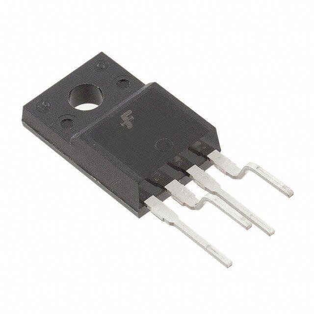
ICGOO电子元器件商城为您提供AP7363-10D-13由Diodes Inc.设计生产,在icgoo商城现货销售,并且可以通过原厂、代理商等渠道进行代购。 AP7363-10D-13价格参考¥3.34-¥7.87。Diodes Inc.AP7363-10D-13封装/规格:PMIC - 稳压器 - 线性, Linear Voltage Regulator IC Positive Fixed 1 Output 1V 1.5A TO-252-3。您可以下载AP7363-10D-13参考资料、Datasheet数据手册功能说明书,资料中有AP7363-10D-13 详细功能的应用电路图电压和使用方法及教程。
AP7363-10D-13 是由 Diodes 公司推出的一款线性稳压器(LDO),属于电源管理集成电路(PMIC)中的一种。该器件主要应用于对电源噪声敏感、要求稳定电压输出的电子系统中。

其典型应用场景包括:

1. 便携式设备供电:如智能手机、平板电脑、可穿戴设备等,适用于电池供电系统中为处理器、传感器或其他低功耗模块提供稳定电压。

2. 通信模块电源管理:用于无线通信模块(如 Wi-Fi、蓝牙、LTE 模块)的电源调节,提供低噪声、高稳定性的供电环境。

3. 工业控制系统:在工业自动化设备中,为精密模拟电路、传感器接口或微控制器单元(MCU)提供干净电源。

4. 音频与射频电路:因其低噪声特性,适合用于音频放大器、射频接收器等对电源纹波敏感的电路中。

5. 测试与测量设备:如示波器、万用表等精密仪器,确保高精度测量所需的稳定电源。

该器件具有低静态电流、高电源抑制比(PSRR)和快速瞬态响应等特点,封装小巧,适合空间受限的设计。其输出电压为固定1.0V,适合为低电压数字电路和模拟电路提供高效稳压。
| 参数 | 数值 |
| 产品目录 | 集成电路 (IC) |
| 描述 | IC REG LDO 1V 1.5A TO252-3 |
| 产品分类 | |
| 品牌 | Diodes Incorporated |
| 数据手册 | |
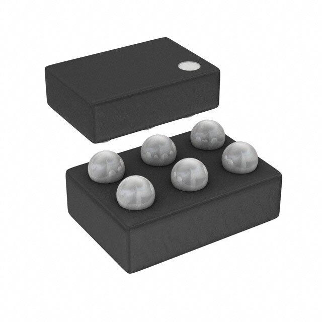
| 产品图片 |
|
| 产品型号 | AP7363-10D-13 |
| rohs | 无铅 / 符合限制有害物质指令(RoHS)规范要求 |
| RoHS指令信息 | http://diodes.com/download/4349 |
| 产品系列 | - |
| 供应商器件封装 | TO-252-3 |
| 其它名称 | AP7363-10D-13TR |
| 包装 | 带卷 (TR) |
| 安装类型 | 表面贴装 |
| 封装/外壳 | TO-252-3,DPak(2 引线+接片),SC-63 |
| 工作温度 | -40°C ~ 85°C |
| 标准包装 | 2,500 |
| 电压-跌落(典型值) | - |
| 电压-输入 | 2.2 V ~ 5.5 V |
| 电压-输出 | 1V |
| 电流-输出 | 1.5A |
| 电流-限制(最小值) | - |
| 稳压器拓扑 | 正,固定式 |
| 稳压器数 | 1 |


- 商务部:美国ITC正式对集成电路等产品启动337调查
- 曝三星4nm工艺存在良率问题 高通将骁龙8 Gen1或转产台积电
- 太阳诱电将投资9.5亿元在常州建新厂生产MLCC 预计2023年完工
- 英特尔发布欧洲新工厂建设计划 深化IDM 2.0 战略
- 台积电先进制程称霸业界 有大客户加持明年业绩稳了
- 达到5530亿美元!SIA预计今年全球半导体销售额将创下新高
- 英特尔拟将自动驾驶子公司Mobileye上市 估值或超500亿美元
- 三星加码芯片和SET,合并消费电子和移动部门,撤换高东真等 CEO
- 三星电子宣布重大人事变动 还合并消费电子和移动部门
- 海关总署:前11个月进口集成电路产品价值2.52万亿元 增长14.8%


PDF Datasheet 数据手册内容提取
AP7363 1.5A LOW QUIESCENT CURRENT, FAST TRANSIENT ULTRA-LOW DROPOUT LINEAR REGULATOR Description Pin Assignments The AP7363 is a 1.5A adjustable-output voltage linear regulator with (Top View) ultra-low dropout. The device includes pass element, error amplifier, ADJ/ band-gap, current limit, and thermal shutdown circuitry. NC OUTOUTOUT 8 7 6 5 The characteristics of low dropout voltage and fast transient response to step changes in load make the device suitable for low-voltage microprocessor applications. The typical quiescent current is approximately 0.5mA and changes little with load current. The built-in current-limit and thermal-shutdown functions prevent IC damage in fault conditions. 1 2 3 4 This device is available in U-DFN2030-8, SO-8EP, SOT223 and GND IN IN IN TO252 packages. U-DFN2030-8 (Top View) Features 1.5A Ultra-Low Dropout Linear Regulator GND 1 8 ADJ/NC Ultra-Low Dropout: 190mV at 1.5A Stable With 10µF Input/Output Capacitor, Any Types IN 2 7 OUT Wide Input Voltage Range: 2.2V to 5.5V IN 3 6 OUT Adjustable Output Voltage: 0.6V to 5.0V Fixed Output Options: 1V, 1.2V, 1.5V, 1.8V, 2.5V, 3.3V IN 4 5 OUT Low Ground Pin Current 25nA Quiescent Current in Shutdown Mode Excellent Load/Line Transient Response SO-8EP Current Limit and Thermal Shutdown Protection (Top View) Ambient Temperature Range: -40°C to +85°C U-DFN2030-8, SO-8EP, SOT223 and TO252: Available in 3 OUT “Green” Molding Compound (No Br, Sb) Totally Lead-Free & Fully RoHS Compliant (Notes 1 & 2) 2 GND (TAB) Halogen and Antimony Free. “Green” Device (Note 3) 1 IN Applications SOT223 ASIC Power Supplies In Printers, Graphics Cards, DVD Players, (Fixed Output) STBs, Routers, and so on (Top View) FPGA and DSP Core or I/O Power Supplies SMPS Regulator 3 Conversion From 3.3V or 5V Rail 2 GND 1 TO252 Notes: 1. No purposely added lead. Fully EU Directive 2002/95/EC (RoHS), 2011/65/EU (RoHS 2) & 2015/863/EU (RoHS 3) compliant. 2. See https://www.diodes.com/quality/lead-free/ for more information about Diodes Incorporated’s definitions of Halogen- and Antimony-free, "Green" and Lead-free. 3. Halogen- and Antimony-free "Green” products are defined as those which contain <900ppm bromine, <900ppm chlorine (<1500ppm total Br + Cl) and <1000ppm antimony compounds. AP7363 1 of 15 June 2018 Document number: DS35059 Rev. 9 - 2 www.diodes.com © Diodes Incorporated
AP7363 Typical Applications Circuit V V V V IN OUT IN OUT IN OUT IN OUT AP7363 AP7363 R1 10µF 10µF 10µF 10µF ADJ GND GND R2 Fixed Output Adjustable Output R V V 1 1 whereR 10kΩ OUT REF 2 R2 Pin Descriptions Pin Number Pin Name SOT223 U-DFN2030-8 Function TO252 SO-8EP GND 2 1 Ground IN 1 2, 3, 4 Voltage Input Pin OUT 3 5, 6, 7 Voltage Output Pin Output feedback pin for adjustable version only—a resistor divider from this pin to ADJ NA 8 the OUT pin and ground sets the output voltage. NC NA 8 No connection for fixed output version. The exposed pad (EP) removes heat from the package, and it is recommended that the EP is connected to a copper area. The die is electrically connected to the EP/TAB — — exposed pad. It is recommended to connect the EP externally to GND, but it should not be the only ground connection. Functional Block Diagram IN OUT IN OUT EN DGraivteer CanSudrhr ueTtnhdteo Lrwmimnailt R EN DGraivteer CanSudrhr ueTtnhdteo Lrwmimnailt ADJ 0.605V 0.605V R GND GND Fixed Version Adjustable Version AP7363 2 of 15 June 2018 Document number: DS35059 Rev. 9 - 2 www.diodes.com © Diodes Incorporated
AP7363 Absolute Maximum Ratings (@TA = +25°C, unless otherwise specified.) Symbol Parameter Ratings Unit ESD HBM Human Body Model ESD Protection 2000 V ESD MM Machine Model ESD Protection 200 V VIN Input Voltage -0.3 to +6.0 V VOUT OUT Voltage -0.3 to VIN +0.3 V IOUT Continuous Load Current Internal Limited — TST Storage Temperature Range -65 to +150 °C TJ Maximum Junction Temperature 150 °C Recommended Operating Conditions (@TA = +25°C, unless otherwise specified.) Symbol Parameter Min Max Unit VIN Input Voltage 2.2 5.5 V IOUT Output Current 0 1.5 A TA Operating Ambient Temperature -40 +85 °C TJ Operating Junction Temperature (Note 5) -40 +125 °C Notes: 4. Stresses beyond those listed under Absolute Maximum Ratings may cause permanent damage to the device. These are stress ratings only and functional operation of the device at these or any other conditions beyond those indicated are not implied. Exposure to absolute-maximum rated conditions for extended periods may affect device reliability. 5. Operating junction temperature must be evaluated and derated as needed, based on ambient temperature (TA), power dissipation (PD), maximum allowable operating junction temperature (TJ-MAX), and package thermal resistance (θJA). AP7363 3 of 15 June 2018 Document number: DS35059 Rev. 9 - 2 www.diodes.com © Diodes Incorporated
AP7363 Electrical Characteristics (@TA = +25°C, VIN = 3.3V, IOUT = 10mA, CIN = 10µF, COUT = 10µF, unless otherwise specified.) Minimum and maximum limits are guaranteed through test, design, or statistical correlation. Typical values represent the most likely parametric norm at T = +25°C, and are provided for reference purposes only. A Symbol Parameter Test Conditions Min Typ Max Unit VADJ ADJ Pin Voltage VIN = VIN-MIN to VIN-MAX, TA = +25°C 0.584 0.605 0.626 V IOUT = 10mA to 1.5A Over temp 0.575 — 0.635 TA = +25°C — 50 — IADJ ADJ Pin Bias Current VIN = VIN-MIN to VIN-MAX nA Over temp — — 750 TA = +25°C — 190 240 VDROPOUT Dropout Voltage (Note 6) IOUT = 1.5A, VOUT = 2.5V mV Over temp — — 280 VOUT / VIN Line Regulation (Note 7) VIN = VIN-MIN to VIN-MAX TA = +25°C — 0.04 — %/V Over temp — 0.05 VOUT / IOUT Load Regulation (Note 7) IOUT = 10mA to 1.5A TA = +25°C — 0.18 — %/A Over temp — 0.33 Ground Pin Current in Normal TA = +25°C — 1.0 1.2 IGND Operation Mode IOUT = 10mA to 1.5A Over temp — — 1.3 mA IOUT-PK Peak Output Current VOUT VOUT - NOM -5% — — A TA = +25°C — 3.7 — ISC Short Circuit Current OUT Grounded A Over temp 2 — — td(off) Turn-Off Delay From VEN < VIL to VOUT = OFF, IOUT = 1.5A — 25 — μs td(on) Turn-On Delay From VEN > VIH to VOUT = ON, IOUT = 1.5A — 25 — μs VIN = 3.0V, IOUT = 1.5A, f = 120Hz — 65 — PSRR Ripple Rejection dB VIN = 3.0V, IOUT = 1.5A, f = 1kHz — 61 — n(l/f) Output Noise Density F = 120Hz, COUT = 10μF Ceramic — 1.0 — µV/Hz BW = 100Hz – 100kHz, — — en Output Noise Voltage COUT = 10μF Ceramic 100 µV(rms) TSHDN Thermal Shutdown Threshold TJ Rising — 170 — °C THYS Thermal Shutdown Hysteresis TJ Falling From TSHDN — 10 — U-DFN2030-8 (Note 8) — 174.0 — Thermal Resistance Junction-to- SO-8EP (Note 8) — 52.8 — ϴJA Ambient SOT223 (Note 8) — 105.7 — °C/W TO252 (Note 8) — 87.8 — U-DFN2030-8 (Note 8) — 28.2 — SO-8EP (Note 8) — 10.0 — ϴJC Thermal Resistance Junction-to-Case °C/W SOT223 (Note 8) — 18.5 — TO252 (Note 8) — 17.3 — Notes: 6. Dropout voltage is the minimum voltage difference between the input and the output at which the output voltage drops 2% below its nominal value. For any output voltage less than 2.5V, the minimum VIN operating voltage is the limiting factor. 7. The line and load regulation specification contains only the typical number. However, the limits for line and load regulation are included in the adjust voltage tolerance specification. 8. Device mounted on 2” × 2” FR-4 substrate PCB, 2oz copper with minimum recommended pad layout. AP7363 4 of 15 June 2018 Document number: DS35059 Rev. 9 - 2 www.diodes.com © Diodes Incorporated
AP7363 Typical Performance Characteristics (@TJ = +25°C, VIN = 2.7V, CIN = 10µF, COUT = 10µF, IOUT = 10mA, VOUT = 1.8V) 10k 10k COUT = 10µF CER COUT = 10µF z) 1k z) 1k H H V/ V/ n n E ( E ( S S OI OI N 100 N 100 10 10 100 1000 10k 100k 100 1000 10k 100k FREQUENCY (Hz) FREQUENCY (Hz) Noise Density Noise Density 3 2 2.5 2 (mA)D 1.5 (V)UT 1 N O G V 25°C I 1 125°C 0.5 -40°C 0 0 0 0.5 1 1.5 0 1 2 3 I (A) V (V) LOAD IN I vs. Load Current Turn-On Characteristics GND 0.615 0.3 0.610 V) 125°C E ( G 0.2 V) 0.605 LTA 25°C (DJ VO VA 0.600 UT O -40°C P O 0.1 R D 0.595 0.590 0 -50 -25 0 25 50 75 100 125 0 0.5 1 1.5 TEMPERATURE (°C) LOAD CURRENT (A) V vs. Temperature Dropout Voltage vs. Load Current ADJ AP7363 5 of 15 June 2018 Document number: DS35059 Rev. 9 - 2 www.diodes.com © Diodes Incorporated
AP7363 Typical Performance Characteristics (continued) (@TJ = +25°C, VIN = 2.7V, CIN = 10µF, COUT = 10µF, IOUT = 10mA, VOUT = 1.8V) Turn-On Time Turn-On Time V = 1.2V (500mV/div) V = 1.2V (500mV/div) OUT OUT I = 1.5A, C = 10μF CER I = 0A, C = 10μF CER L OUT L OUT V = 3.0V (2V/div) V = 3.0V (2V/div) IN IN Time (10μs/div) Time (10μs/div) Load Transient Response 90 V = 3.3V IN COUT =10μF CER 80 70 B) O (d 60 V = 1.8V (50mV/div) OUT TI A 50 R N O 40 TI C 30 E EJ VIN = 3.3V R 20 VOUT = 1.8V IOUT = 1A 10 CIN = 1µF CER ILOAD = 100mA to 1.5A (1A/div) COUT = 1µF CER 0 100 1k 10k 100k 1M FREQUENCY (kHz) PSRR Time (40μs/div) AP7363 6 of 15 June 2018 Document number: DS35059 Rev. 9 - 2 www.diodes.com © Diodes Incorporated
AP7363 Application Note Input Capacitor A minimum 2.2μF ceramic capacitor is recommended between IN and GND pins to decouple input power supply glitch and noise. The amount of the capacitance can be increased without limit. A larger input capacitor, like 10μF, provides better load transient response. This input capacitor must be located as close as possible to the device to assure input stability and to reduce noise. For PCB layout, a wide copper trace is required for both IN and GND pins. A lower ESR capacitor type allows the use of less capacitance, while a higher ESR type requires more capacitance. Output Capacitor The output capacitor is required to stabilize and help the transient response of the LDO. The AP7363 is stable with any type of capacitor with no limitations on minimum or maximum ESR. The device is designed to have excellent transient response for most applications with a small amount of output capacitance. The device is also stable with multiple capacitors in parallel, which can be of any type of value. Additional capacitance helps reduce undershoot and overshoot during transient loads. This capacitor must be placed as close as possible to OUT and GND pins for optimum performance. Adjustable Operation The AP7363 provides output voltage from 0.6V to 5.0V through external resistor divider as shown below. The output voltage is calculated by the following equation: R VOUT VREF1R1 2 Where VREF = 0.6V (the internal reference voltage) Rearranging the previous equation gives the following equation that is used for adjusting the output to a particular voltage: V R R OUT 1 1 2V REF To maintain the stability of the internal reference voltage, R2 must be kept smaller than 10kΩ. No Load Stability Other than external resistor divider, no minimum load is required to keep the device stable. The device will remain stable and regulated in no load condition. AP7363 7 of 15 June 2018 Document number: DS35059 Rev. 9 - 2 www.diodes.com © Diodes Incorporated
AP7363 Application Note (continued) Stability and Phase Margin Any regulator that operates using a feedback loop must be compensated in such a way as to ensure adequate phase margin, which is defined as the difference between the phase shift and -180 degrees at the frequency where the loop gain crosses unity (0 dB). For most LDO regulators, the ESR of the output capacitor is required to create a zero to add enough phase lead to ensure stable operation. The AP7363 has an internal compensation circuit that maintains phase margin regardless of the ESR of the output capacitor—any type of capacitors can be used. The following charts show the gain/phase plot of the AP7363 with an output of 1.2V, 10μF ceramic output capacitor, and delivering 1.5A load current and no load. The phase margin is about 90°, which is very stable. 120 140 120 140 100 PHASE 120 100 120 80 100 80 PHASE 100 60 GAIN 80 60 80 LOOP GAIN (dB) --244200000 6420000 ASE MARGIN (°) LOOP GAIN (dB) --244200000 GAIN 6420000 ASE MARGIN (°) H H -1--086000 VVICLIOO N=UU =1TT . 25==.A 711V.02µVF CER ---246000 P -1--086000 VVICLIOO N=UU =T0T A 2==. 711V.02µVF CER ---246000 P -120 -80 -120 -80 100 1k 10k 100k 1M 100 1k 10k 100k 1M FREQUENCY(Hz) FREQUENCY(Hz) Gain-Bandwidth Plot for 1.5A Load Gain-Bandwidth Plot for no Load Short-Circuit Protection When the output current at the OUT pin is higher than the current limit threshold, the current limit protection triggers and clamps the output current to prevent overcurrent and to protect the regulator from damage due to overheating. Thermal Shutdown Protection Thermal protection disables the output when the junction temperature rises to approximately +170°C, which allows the device to cool down. When the junction temperature reduces to approximately +160°C, the output circuitry is enabled again. Depending on power dissipation, thermal resistance, and ambient temperature, the thermal protection circuit may cycle on and off. This cycling limits the heat dissipation of the regulator and protects it from damage due to overheating. Low Quiescent Current The AP7363, consuming only around 0.5mA for all input range, provides great power saving in portable and low-power applications. Output Noise This is the integrated value of the output noise over a specified frequency range. Input voltage and output load current are kept constant during the measurement. Results are expressed in µVrms or µV√Hz. The AP7363 is a low-noise regulator and requires no external noise reduction capacitor. Output voltage noise is typically 100μVrms, and overall noise level is between 100 Hz and 100 kHz. Noise is specified in two ways: Output noise density is the RMS sum of all noise sources, measured at the regulator output, at a specific frequency (measured with a 1Hz bandwidth). This type of noise is usually plotted on a curve as a function of frequency. Output noise voltage is the RMS sum of spot noise over a specified bandwidth. Spot noise is measured in units µV/√Hz or nV/√Hz, and total output noise is measured in µV(rms). The primary source of noise in low-dropout regulators is the internal reference. AP7363 8 of 15 June 2018 Document number: DS35059 Rev. 9 - 2 www.diodes.com © Diodes Incorporated
AP7363 Application Note (cont.) Power Dissipation The device power dissipation and proper sizing of the thermal plane connected to the thermal pad is critical to avoid thermal shutdown and ensure reliable operation. Power dissipation of the device depends on input voltage and load conditions and can be calculated by: PD = (VIN - VOUT) × IOUT The maximum power dissipation, handled by the device, depends on the junction-to-ambient thermal resistance and maximum ambient temperature, which can be calculated by the following equation: (150C-T ) A P D_max R JA Ordering Information AP7363- XX XX- XX Output Package Packing 7/13 : Tape & Reel BLANK : ADJ HA : U-DFN203 10 : 1.0V SP : SO-8EP 12 : 1.2V E : SOT223-3L 15 : 1.5V D : TO252-3L 18 : 1.8V 25 : 2.5V 33 : 3.3V Packaging 7”/13” Tape and Reel Part Number Package Code (Note 9) Quantity Part Number Suffix AP7363-XXHA-7 HA U-DFN2030-8 3000/Tape & Reel -7 AP7363-XXSP-13 SP SO-8EP 2500/Tape & Reel -13 AP7363-XXE-13 E SOT223-3L 2500/Tape & Reel -13 AP7363-XXD-13 D TO252-3L 2500/Tape & Reel -13 Note: 9. TO252 and SOT223 are only available with fixed output version. Marking Information (1) U-DFN2030-8 ( Top View ) XX : Identification Code XX Y : Year : 0~9 Y WX W : Week : A~Z : 1~26 week; a~z : 27~52 week; z represents 52 and 53 week X : Internal Code Device Package Identification Code AP7363ADJ U-DFN2030-8 SA AP7363-10 U-DFN2030-8 SB AP7363-12 U-DFN2030-8 SC AP7363-15 U-DFN2030-8 SD AP7363-18 U-DFN2030-8 SE AP7363-25 U-DFN2030-8 SF AP7363-33 U-DFN2030-8 SG AP7363 9 of 15 June 2018 Document number: DS35059 Rev. 9 - 2 www.diodes.com © Diodes Incorporated
AP7363 Marking Information (continued) (2) SO-8EP ( Top View ) 8 5 YY : Year : 08, 09,10~ Logo WW : Week : 01~52; 52 Part Number AP7363-VV represents 52 and 53 week YYWWXXE XX : Internal Code AP7363 for ADJ AP7363-10 for 1.0V SO-8-EP AP7363-12 for 1.2V 1 4 AP7363-15 for 1.5V AP7363-18 for 1.8V AP7363-25 for 2.5V AP7363-33 for 3.3V (3) SOT223 ( Top View ) Y : Year : 0~9 Logo Y W X W : Week : A~Z : 1~26 week; a~z : 27~52 week; Part Number 6 3-VV z repersents 52 and 53 week X : Internal Code 63 for ADJ 63-VV:10 for 1.0V 12 for 1.2V 15 for 1.5V 18 for 1.8V 25 for 2.5V 33 for 3.3V (4) TO252 ( Top View ) Logo 63-VV YY : Year : 01~09 Part Number YY WW Xx WW : Week : 01~52, 52 represents 63-VV : 10 for 1.0V 52 and 53 week 12 for 1.2V Xx : Internal Code 15 for 1.5V 18 for 1.8V 25 for 2.5V 33 for 3.3V AP7363 10 of 15 June 2018 Document number: DS35059 Rev. 9 - 2 www.diodes.com © Diodes Incorporated
AP7363 Package Outline Dimensions (All dimensions in mm.) Please see http://www.diodes.com/package-outlines.html for the latest version. 1) U-DFN2030-8 A A1 A3 U-DFN2030-8 Seating Plane Dim Min Max Typ A 0.57 0.63 0.60 D A1 0 0.05 0.02 e L A3 - - 0.15 (Pin #1 ID) b 0.20 0.30 0.25 D 1.95 2.05 2.00 D2 1.40 1.60 1.50 e - - 0.50 E 2.95 3.05 3.00 C'0.25*45° E2 1.50 1.70 1.60 E E2 L 0.35 0.45 0.40 D2 Z - - 0.125 All Dimensions in mm z b 2) SO-8EP SO-8EP EXPOSED PAD F Dim Min Max Typ A 1.40 1.50 1.45 A1 0.00 0.13 - E1 H b 0.30 0.50 0.40 C 0.15 0.25 0.20 1 D 4.85 4.95 4.90 E 3.80 3.90 3.85 E0 3.85 3.95 3.90 b E1 5.90 6.10 6.00 E 9° (All side) N Q Fe 2.-7 5 3.-3 5 13..2075 7° 45° C H 2.11 2.71 2.41 °3±°4 Gauge Plane L 0.62 0.82 0.72 Seating Plane N - - 0.35 R 0.1 A L Q 0.60 0.70 0.65 e A1 E0 All Dimensions in mm D AP7363 11 of 15 June 2018 Document number: DS35059 Rev. 9 - 2 www.diodes.com © Diodes Incorporated
AP7363 Package Outline Dimensions (continued) (All dimensions in mm.) Please see http://www.diodes.com/package-outlines.html for the latest version. 3) SOT223 D b1 Q C SOT223 Dim Min Max Typ A 1.55 1.65 1.60 A1 0.010 0.15 0.05 E E1 b 0.60 0.80 0.70 b1 2.90 3.10 3.00 Gauge Plane C 0.20 0.30 0.25 0.25 D 6.45 6.55 6.50 Seating L E 3.45 3.55 3.50 Plane E1 6.90 7.10 7.00 e1 e b 0°-10° ee1 -- -- 42..6300 L 0.85 1.05 0.95 Q 0.84 0.94 0.89 A A1 All Dimensions in mm 7° 7° 4) TO252 (Standard) E TO252 (S tandard) A b3 Dim Min Max Typ L3 7°±1° c A 2.19 2.39 2.29 A1 0.00 0.13 0.08 E1 D1 A2 0.97 1.17 1.07 D A2 H Gauge Plane 0.508 A1 bb2 00..6746 01..8184 00..79853 b3 5.21 5.46 5.33 L4 a L c 0.45 0.58 0.531 Seating Plane 2.74REF D 6.00 6.20 6.10 e b(3x) D1 5.21 - - b2(2x) e - - 2.286 E 6.45 6.70 6.58 E1 4.32 - - H 9.40 10.41 9.91 L 1.40 1.78 1.59 L3 0.88 1.27 1.08 L4 0.60 1.02 0.83 a 0° 10° - Option A Option B Option A Option B (Top View) (Top View) (Bottom View) (Bottom View) All Dimensions in mm AP7363 12 of 15 June 2018 Document number: DS35059 Rev. 9 - 2 www.diodes.com © Diodes Incorporated
AP7363 Suggested Pad Layout Please see http://www.diodes.com/package-outlines.html for the latest version. 1) U-DFN2030-8 X2 C Y Value Dimensions (in mm) C 0.500 G 0.250 X 0.350 Y2 Y1 X1 1.500 X2 1.850 X1 Y 0.600 Y1 1.600 Y2 3.300 G Pin1 X 2) SO-8EP X2 Value Dimensions (in mm) C 1.270 Y1 X 0.802 Y2 X1 3.502 X1 X2 4.612 Y 1.505 Y1 2.613 Y Y2 6.500 C X AP7363 13 of 15 June 2018 Document number: DS35059 Rev. 9 - 2 www.diodes.com © Diodes Incorporated
AP7363 Suggested Pad Layout (continued) Please see http://www.diodes.com/package-outlines.html for the latest version. 3) SOT223 X1 Y1 Dimensions Value (in mm) C 2.30 C1 6.40 C1 Y2 X 1.20 X1 3.30 Y 1.60 Y1 1.60 Y2 8.00 Y X C 4) TO252 (Standard) X1 Y1 Dimensions Value (in mm) C 4.572 X 1.060 Y2 X1 5.632 Y 2.600 C Y1 5.700 Y2 10.700 Y X AP7363 14 of 15 June 2018 Document number: DS35059 Rev. 9 - 2 www.diodes.com © Diodes Incorporated
AP7363 IMPORTANT NOTICE DIODES INCORPORATED MAKES NO WARRANTY OF ANY KIND, EXPRESS OR IMPLIED, WITH REGARDS TO THIS DOCUMENT, INCLUDING, BUT NOT LIMITED TO, THE IMPLIED WARRANTIES OF MERCHANTABILITY AND FITNESS FOR A PARTICULAR PURPOSE (AND THEIR EQUIVALENTS UNDER THE LAWS OF ANY JURISDICTION). Diodes Incorporated and its subsidiaries reserve the right to make modifications, enhancements, improvements, corrections or other changes without further notice to this document and any product described herein. Diodes Incorporated does not assume any liability arising out of the application or use of this document or any product described herein; neither does Diodes Incorporated convey any license under its patent or trademark rights, nor the rights of others. Any Customer or user of this document or products described herein in such applications shall assume all risks of such use and will agree to hold Diodes Incorporated and all the companies whose products are represented on Diodes Incorporated website, harmless against all damages. Diodes Incorporated does not warrant or accept any liability whatsoever in respect of any products purchased through unauthorized sales channel. Should Customers purchase or use Diodes Incorporated products for any unintended or unauthorized application, Customers shall indemnify and hold Diodes Incorporated and its representatives harmless against all claims, damages, expenses, and attorney fees arising out of, directly or indirectly, any claim of personal injury or death associated with such unintended or unauthorized application. Products described herein may be covered by one or more United States, international or foreign patents pending. Product names and markings noted herein may also be covered by one or more United States, international or foreign trademarks. This document is written in English but may be translated into multiple languages for reference. Only the English version of this document is the final and determinative format released by Diodes Incorporated. LIFE SUPPORT Diodes Incorporated products are specifically not authorized for use as critical components in life support devices or systems without the express written approval of the Chief Executive Officer of Diodes Incorporated. As used herein: A. Life support devices or systems are devices or systems which: 1. are intended to implant into the body, or 2. support or sustain life and whose failure to perform when properly used in accordance with instructions for use provided in the labeling can be reasonably expected to result in significant injury to the user. B. A critical component is any component in a life support device or system whose failure to perform can be reasonably expected to cause the failure of the life support device or to affect its safety or effectiveness. Customers represent that they have all necessary expertise in the safety and regulatory ramifications of their life support devices or systems, and acknowledge and agree that they are solely responsible for all legal, regulatory and safety-related requirements concerning their products and any use of Diodes Incorporated products in such safety-critical, life support devices or systems, notwithstanding any devices- or systems-related information or support that may be provided by Diodes Incorporated. Further, Customers must fully indemnify Diodes Incorporated and its representatives against any damages arising out of the use of Diodes Incorporated products in such safety-critical, life support devices or systems. Copyright © 2018, Diodes Incorporated www.diodes.com AP7363 15 of 15 June 2018 Document number: DS35059 Rev. 9 - 2 www.diodes.com © Diodes Incorporated
Mouser Electronics Authorized Distributor Click to View Pricing, Inventory, Delivery & Lifecycle Information: D iodes Incorporated: AP7363-10D-13 AP7363-12D-13 AP7363-15D-13 AP7363-18D-13 AP7363-25D-13 AP7363-33D-13 AP7363-HA-7