ICGOO在线商城 > 集成电路(IC) > PMIC - 稳压器 - 线性 > AP2318M-ADJTRG1
 Datasheet下载
- 型号: AP2318M-ADJTRG1
- 制造商: Diodes Inc.
- 库位|库存: xxxx|xxxx
- 要求:
| 数量阶梯 | 香港交货 | 国内含税 |
| +xxxx | $xxxx | ¥xxxx |
查看当月历史价格
查看今年历史价格
AP2318M-ADJTRG1产品简介:
ICGOO电子元器件商城为您提供AP2318M-ADJTRG1由Diodes Inc.设计生产,在icgoo商城现货销售,并且可以通过原厂、代理商等渠道进行代购。 AP2318M-ADJTRG1价格参考。Diodes Inc.AP2318M-ADJTRG1封装/规格:PMIC - 稳压器 - 线性, Linear Voltage Regulator IC Positive Adjustable 1 Output Adj to 0.8V 600mA 8-SOIC。您可以下载AP2318M-ADJTRG1参考资料、Datasheet数据手册功能说明书,资料中有AP2318M-ADJTRG1 详细功能的应用电路图电压和使用方法及教程。
Diodes Incorporated的AP2318M-ADJTRG1是一款低噪声、低压差(LDO)线性稳压器,适用于多种应用场景。该器件具有可调输出电压功能,能够在1.2V至5.5V范围内调节输出电压,适用于需要精确电压控制的系统。

 主要应用场景:

 1. 便携式电子设备
   AP2318M-ADJTRG1广泛应用于便携式电子设备中,如智能手机、平板电脑、可穿戴设备等。这些设备通常依赖电池供电,因此对电源管理芯片的要求较高。AP2318M-ADJTRG1的低静态电流(典型值为10µA)和高效率特性使其非常适合用于延长电池寿命。此外,其低噪声特性有助于减少对敏感电路(如射频模块、音频电路)的干扰,确保设备性能稳定。

 2. 通信设备
   在通信设备中,如路由器、调制解调器、无线接入点等,AP2318M-ADJTRG1可以为各种微控制器、传感器和其他外围设备提供稳定的电源。由于其低压差特性,即使在输入电压波动较大的情况下,也能保持输出电压的稳定性,确保通信系统的可靠运行。

 3. 工业自动化
   在工业自动化领域,AP2318M-ADJTRG1可用于为传感器、执行器、PLC(可编程逻辑控制器)等设备供电。工业环境中的电源波动较大,而AP2318M-ADJTRG1的高压差特性使其能够在这种环境下保持稳定的输出电压,确保设备的正常工作。此外,其过流保护和热关断功能也增强了系统的安全性。

 4. 消费类电子产品
   对于消费类电子产品,如智能家居设备、音频播放器、数码相机等,AP2318M-ADJTRG1可以为音频放大器、显示屏驱动器等组件提供干净、稳定的电源。其低噪声特性有助于提高音频质量,减少图像显示中的噪点,提升用户体验。

 5. 汽车电子
   在汽车电子系统中,AP2318M-ADJTRG1可以为车载信息娱乐系统、导航系统、摄像头模块等提供电源。汽车环境中电源波动较大,且温度范围较广,而AP2318M-ADJTRG1的宽工作温度范围(-40°C至+125°C)和良好的抗噪能力使其成为理想选择。

总之,AP2318M-ADJTRG1凭借其低噪声、低压差、高精度输出电压调节等优点,适用于多种需要高效、稳定电源管理的应用场景。
| 参数 | 数值 |
| 产品目录 | 集成电路 (IC) |
| 描述 | IC REG LDO ADJ 0.6A 8SOIC |
| 产品分类 | |
| 品牌 | Diodes Incorporated |
| 数据手册 | |
| 产品图片 |
|
| 产品型号 | AP2318M-ADJTRG1 |
| rohs | 无铅 / 符合限制有害物质指令(RoHS)规范要求 |
| RoHS指令信息 | http://diodes.com/download/4349 |
| 产品系列 | - |
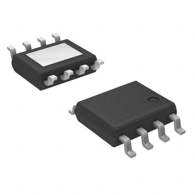
| 供应商器件封装 | 8-SOIC |
| 其它名称 | AP2318M-ADJTRG1DICT |
| 包装 | 剪切带 (CT) |
| 安装类型 | 表面贴装 |
| 封装/外壳 | 8-SOIC(0.154",3.90mm 宽) |
| 工作温度 | -40°C ~ 125°C |
| 标准包装 | 1 |
| 电压-跌落(典型值) | 0.35V @ 600mA |
| 电压-输入 | 2.5 V ~ 12 V |
| 电压-输出 | 可调至 0.8V |
| 电流-输出 | 600mA |
| 电流-限制(最小值) | - |
| 稳压器拓扑 | 正,可调式 |
| 稳压器数 | 1 |


- 商务部:美国ITC正式对集成电路等产品启动337调查
- 曝三星4nm工艺存在良率问题 高通将骁龙8 Gen1或转产台积电
- 太阳诱电将投资9.5亿元在常州建新厂生产MLCC 预计2023年完工
- 英特尔发布欧洲新工厂建设计划 深化IDM 2.0 战略
- 台积电先进制程称霸业界 有大客户加持明年业绩稳了
- 达到5530亿美元!SIA预计今年全球半导体销售额将创下新高
- 英特尔拟将自动驾驶子公司Mobileye上市 估值或超500亿美元
- 三星加码芯片和SET,合并消费电子和移动部门,撤换高东真等 CEO
- 三星电子宣布重大人事变动 还合并消费电子和移动部门
- 海关总署:前11个月进口集成电路产品价值2.52万亿元 增长14.8%


PDF Datasheet 数据手册内容提取
AP2318 600mA ULDO REGULATOR WITH ENABLE Description Pin Assignments The AP2318 is a series of ultra low dropout regulators optimized for low voltage applications where transient response and minimum input (Top View) voltage are critical. The AP2318 provides current limit and thermal shutdown. Its circuit includes a trimmed bandgap reference to assure output voltage accuracy to be within ±1.5%. On-chip thermal shutdown provides protection against any combination of overload and ambient temperatures that would create excessive junction temperatures. The AP2318 has both fixed and adjustable versions. The 1.3V fixed versions integrate the corresponding resistor divider. The adjustable version can set the output voltage through two external resistors. DFN-3x3-8 The AP2318 is available in the standard DFN-3x3-8 and SOIC-8 (Top View) packages. Features NC 1 8 GND Wide Operating Voltage Ranges: 2.5V to 12V EN 2 7 ADJ/NC Output Voltage Accuracy: ±1.5% VIN 3 6 VOUT On-chip Thermal Shutdown ESD VIN 4 5 NC Human Body Model 3kV Machine Model 600V SOIC-8 Operating Junction Temperature: -40°C to +125°C Applications Notebook USB Device Add-on Card DVD Player PC Motherboard AP2318 1 of 13 July 2018 Document number: DS41226 Rev. 2 - 2 www.diodes.com © Diodes Incorporated
AP2318 Typical Applications Circuit V V IN OUT VIN VOUT AP2318-ADJ R1 ADJ/ EN NC GND + COUT CIN + 2.2F 1F R2 ADJ Version, V = 0.8*(R1+R2)/R2 OUT VIN=3.3V VOUT=1.3V VIN VOUT AP2318-1.3 ADJ/ EN NC GND + COUT CIN + 2.2F 1F Fixed 1.3V Version, V = 1.3V OUT Pin Description Pin Number Pin Name Function DFN-3x3-8 SOIC-8 1, 2 3, 4 VIN Input Voltage 3, 4 6 VOUT Output Voltage 5 7 ADJ/NC Adjust Voltage/No Connection 6 8 GND Ground 7 1, 5 NC No Connection 8 2 EN On/Off Control AP2318 2 of 13 July 2018 Document number: DS41226 Rev. 2 - 2 www.diodes.com © Diodes Incorporated
AP2318 Functional Block Diagram V 1, 2 (3, 4) 3, 4 (6) IN V OUT 8 (2) EN RC Enable OVP Compensation 5 (7) ADJ/NC Bandgap Error A1 B Reference V FB Amplifier Thermal Current A2 Shutdown Limit 6 (8) GND Connect A1 and A2, disconnect B: Fixed Voltage Version Connect B, disconnect A1 and A2:Adjustable Voltage Version A(B) A: DFN-3x3-8 B: SOIC-8 Absolute Maximum Ratings (Note 1) Symbol Parameter Rating Unit VIN Input Voltage 15 V TJ Operating Junction Temperature +150 °C TSTG Storage Temperature Range -65 to +150 °C TLEAD Lead Temperature (Soldering, 10sec) +260 °C SOIC-8 135 θJA Thermal Resistance (Note 2) °C/W DFN-3x3-8 120 ESD ESD (Human Body Model) 3000 V ESD ESD (Machine Model) 600 V Notes: 1. Stresses greater than those listed under “Absolute Maximum Ratings” may cause permanent damage to the device. These are stress ratings only, and functional operation of the device at these or any other conditions beyond those indicated under “Recommended Operating Conditions” is not implied. Exposure to “Absolute Maximum Ratings” for extended periods may affect device reliability. 2. Absolute maximum ratings indicate limits beyond which damage to the component may occur. Electrical specifications do not apply when operating the device outside of its operating ratings. The maximum allowable power dissipation is a function of the maximum junction temperature, TJ(max), the junction- to-ambient thermal resistance, θJA, and the ambient temperature, TA. The maximum allowable power dissipation at any ambient temperature is calculated using: PD(max) = (TJ(max)-TA)/θJA. Exceeding the maximum allowable power dissipation will result in excessive die temperature, and the regulator will go into thermal shutdown. AP2318 3 of 13 July 2018 Document number: DS41226 Rev. 2 - 2 www.diodes.com © Diodes Incorporated
AP2318 Recommended Operating Conditions Symbol Parameter Min Max Unit VIN Input Voltage 2.5 12 V VEN Enable Voltage — 12 V TJ Operating Junction Temperature Range -40 +125 °C Electrical Characteristics (Operating Conditions: 2.5V ≤ VIN ≤ 12V, CIN = 1µF, COUT = 2.2µF, TJ = +25°C, unless otherwise specified. (P ≤ Maximum Power Dissipation). Limits appearing in Boldface type apply over the entire junction temperature range for operation of - 40°C to +125°C.) Symbol Parameter Conditions Min Typ Max Unit AP2318-ADJ IOUT = 10mA, VIN-VOUT = 2V, TJ = +25°C 0.788 0.800 0.812 VREF Reference Voltage V 10mA ≤ IOUT ≤ 600mA, VOUT+2V ≤ VIN ≤ 12V 0.784 0.800 0.816 IOUT = 10mA, VIN = 2.5V, TJ = +25°C -1.5% 1.5% VOUT Output Voltage — V 10mA ≤ IOUT ≤ 600mA, 2.5V ≤ VIN ≤ 12V -2% 2% IOUT(max) Maximum Output Current VIN-VOUT = 2V 0.85 1.2 — A AP2318-ADJ — 1 6 mV VRLINE Line Regulation IOUT = 10mA, VOUT+2V ≤ VIN ≤ 12V IOUT = 10mA, 2.5V ≤ VIN ≤ 12V — 1 6 mV AP2318-ADJ — 1 10 mV VRLOAD Load Regulation VIN = VOUT+2V, 10mA ≤ IOUT ≤ 600mA VIN = 2.5V, 10mA ≤ IOUT ≤ 600mA — 1 10 mV VDROP Dropout Voltage ∆VOUT (∆VREF) = 1%, IOUT = 600mA — 0.35 — V IADJ Adjust Pin Current — — 0.05 1 µA ILOAD(min) Minimum Load Current VOUT+2V ≤ VIN ≤ 12V (ADJ only) — 1.7 5 mA IQ Quiescent Current VIN = VOUT+2V, IOUT = 0mA — 250 — µA RMS Output Noise VNOI TA = +25°C, 10Hz ≤ f ≤ 20kHz — 0.003 — % (% of VOUT) Thermal Shutdown — — — +150 — °C Temperature Thermal Shutdown — — — +25 — °C Hysteresis Enable Logic Low — — 0.8 VEN Enable Input Voltage V Enable Logic High 2.25 — — VEN = 2.25V — 5 15 µA IEN Enable Input Current VEN = 0.8V — — 4 µA DFN-3x3-8 — 15 — Thermal Resistance θJC °C/W (Junction to Case) SOIC-8 — 24 — AP2318 4 of 13 July 2018 Document number: DS41226 Rev. 2 - 2 www.diodes.com © Diodes Incorporated
AP2318 Performance Characteristics Output Voltage vs. Output Current Output Voltage vs. Output Current (Conditions: V = 0.8V, ADJ Short to GND) (Conditions: V = 1.2V, R1 = 3kΩ, R2 = 6.2kΩ) OUT OUT 0.90 1.30 0.88 AP2318-ADJ 1.28 AP2318-ADJ V =0.8V V =1.2V 0.86 AODUJT short to GND 1.26 RO1U=T3k ge (V) 00..8824 TVCIN==225.o8CV age (V) 11..2224 RTVC2=IN=2=653.2o.2CkV olta 0.80 Volt 1.20 ut V 0.78 put 1.18 utp Out O 0.76 1.16 0.74 1.14 0.72 1.12 0.70 1.10 0 50 100 150 200 250 300 0 50 100 150 200 250 300 Output Current (mA) Output Current (mA) Output Voltage vs. Output Current Output Voltage vs. Output Current (Conditions: V = 0.8V, ADJ Short to GND) (Conditions: V = 1.2V, R1 = 3kΩ, R2 = 6.2kΩ) OUT OUT 1.0 1.5 0.9 1.4 AP2318-ADJ 1.3 V =1.2V 0.8 1.2 RO1U=T3k 1.1 R2=6.2k Output Voltage (V) 0000....4567 AVATCOPD=U2JT23 =s510ho8.Co8-rVAt DtoJ GND utput Voltage (V) 000001......567890 TC=25oC 0.3 O 0.4 V =3.2V 0.2 VIN=3.2V 0.3 VIN=2.5V 0.1 V VININ==81V2V 00..12 VIINN=12V 0.0 0.0 0 150 300 450 600 750 900 1050 1200 1350 1500 0 150 300 450 600 750 900 1050 1200 1350 1500 Output Current (mA) Output Current (mA) Output Voltage vs. Output Current Output Voltage vs. Output Current (Conditions: VOUT = 0.8V, ADJ Short to GND) (Conditions: VOUT = 1.2V, R1 = 3kΩ, R2 = 6.2kΩ) 1.1 1.5 1.4 1.0 1.3 0.9 1.2 0.8 1.1 Output Voltage (V) 0000000.......1234567 AVVAIOPDNU=2JT23 =s .10TTTh88.CCCoV8===-rVAt2-1 4Dt52o05oJ CoGoCCND Output Voltage (V) 0000000001..........1234567890 AVVRRIOP12NU===2T3363=.k.1 122TTT8.Vk2CCC-===VA2-1D4520J5oCooCC 0.0 0.0 0 150 300 450 600 750 900 1050 1200 1350 1500 0 150 300 450 600 750 900 1050 1200 1350 1500 Output Current (mA) Output Current (mA) AP2318 5 of 13 July 2018 Document number: DS41226 Rev. 2 - 2 www.diodes.com © Diodes Incorporated
AP2318 Performance Characteristics (Cont.) Output Voltage vs. Input Voltage Output Voltage vs. Input Voltage (Conditions: V = 0.8V, ADJ Short to GND) (Conditions: V = 1.2V, R1 = 3kΩ, R2 = 6.2kΩ) OUT OUT 1.0 VCC=5V 1.4 0.9 0.8 1.2 0.7 Output Voltage (V) 0000....3456 AVATCOPD=U2JT23 =s510ho8.Co8-rVAt DtoJ GND Output Voltage (V) 001...680 AVRRTCOP12=U==2T2363=5k.112o8.Ck2-VADJ 300mA 0.4 300mA 0.2 10mA 10mA 600mA 0.2 600mA 0.1 0.0 0.0 0 1 2 3 4 5 6 7 8 9 10 11 12 0 1 2 3 4 5 6 7 8 9 10 11 12 Input Voltage (V) Input Voltage (V) Output Voltage vs. Case Temperature Output Voltage vs. Case Temperature (Conditions: V = 0.8V, ADJ Short to GND) (Conditions: V = 1.2V, R1 = 3kΩ, R2 = 6.2kΩ) OUT OUT 0.90 1.30 0.88 1.28 AP2318-ADJ V =3.2V 0.86 1.26 IN V =1.2V oltage (V) 000...888024 Voltage (V) 111...222024 RRIOO12UUT===T361k.02mkA ut V 0.78 put 1.18 Outp 0.76 AVIPN=223.188V-ADJ Out 1.16 V =0.8V 0.74 AODUJT short to GND 1.14 0.72 IOUT=10mA 1.12 0.70 1.10 -40 -20 0 20 40 60 80 100 120 -40 -20 0 20 40 60 80 100 120 Case Temperature (oC) Case Temperature (oC) Supply Voltage vs. Input Voltage Supply Voltage vs. Input Voltage (Conditions: V = 0.8V, ADJ Short to GND) (Conditions: V = 1.2V, R1 = 3kΩ, R2 = 6.2kΩ) OUT OUT 250 400 225 350 200 300 A) 175 A) Current ( 112550 AVAOPDU2JT3 =s10h8.o8-rVAt DtoJ GND Current ( 220500 AVRROP12U==2T363=k.1128.k2-VADJ ply 100 No Load ply 150 No Load up T =-40oC up T =-40oC S 75 C S C T =25oC 100 T =25oC C C 50 T =125oC T =125oC C 50 C 25 0 0 0 1 2 3 4 5 6 7 8 0 1 2 3 4 5 6 7 8 Input Voltage (V) Input Voltage (V) AP2318 6 of 13 July 2018 Document number: DS41226 Rev. 2 - 2 www.diodes.com © Diodes Incorporated
AP2318 Performance Characteristics (Cont.) Supply Current vs. Case Temperature Supply Current vs. Case Temperature (Conditions: V = 0.8V, ADJ Short to GND) (Conditions: V = 1.2V, R1 = 3kΩ, R2 = 6.2kΩ) OUT OUT VCC=5V 220 340 216 336 AP2318-ADJ 212 AVP=223.188V-ADJ 332 VVIN=3=.12.V2V nt (A) 220048 VANIODoNU JTL =os0ha.od8rVt to GND nt (A) 332248 RRNO12oU== TL36ok.a2dk e e Curr 200 Curr 320 y y pl 196 pl 316 p p Su 192 Su 312 188 308 184 304 180 300 -40 -20 0 20 40 60 80 100 120 -40 -20 0 20 40 60 80 100 120 Case Temperature (oC) Case Temperature (oC) Supply Current vs. Output Current Supply Current vs. Output Current (Conditions: V = 0.8V, ADJ Short to GND) (Conditions: V = 1.2V, R1 = 3kΩ, R2 = 6.2kΩ) OUT OUT 20 20 18 18 16 16 mA) 14 AP2318-ADJ A) 14 Supply Current ( 116802 VVAIODNU=JT2 =s. 0h8TT.oV8CCr==Vt2- t45o0o GCoCND Supply Current (m 110268 AVVRRIOP12NU===2T3363=. k.112T28.VkC2-=VA2D5JoC 4 TC=125oC 4 TC=-40oC T =125oC 2 2 C 0 0 0 150 300 450 600 750 900 1050 1200 1350 1500 0 150 300 450 600 750 900 1050 1200 1350 1500 Output Current (mA) Output Current (mA) Supply Current vs. Output Current Supply Current vs. Output Current (Conditions: V = 0.8V, ADJ Short to GND) (Conditions: V = 1.2V, R1 = 3kΩ, R2 = 6.2kΩ) OUT OUT 20 20 18 18 16 16 A) 14 A) 14 Supply Current (m 116802 AVATCOPD=U2JT2 3=s510 hoVV8.Co8I-NrVA==t Dt38o.VJ 2GVND Supply Current (m 110268 AVRRTCOP12=U==2T2363=5k.11 2oV8.Ck2-VA=D3.J2V VIN=12V VIN=2.5V 4 IN 4 IN V =12V IN 2 2 0 0 0 150 300 450 600 750 900 1050 1200 1350 1500 0 150 300 450 600 750 900 1050 1200 1350 1500 Output Current (mA) Output Current (mA) AP2318 7 of 13 July 2018 Document number: DS41226 Rev. 2 - 2 www.diodes.com © Diodes Incorporated
AP2318 Performance Characteristics (Cont.) Load Transient Response Load Transient Response (Conditions: V = 2.5V, V = 1.3V, I = 1mA to 300mA, (Conditions: V = 2.5V, V = 1.8V, I = 1mA to 600mA, IN OUT OUT IN OUT OUT C = 1µF, C = 2.2µF) C = 1µF, C = 2.2µF) IN OUT IN OUT Div) Div) A/ A/ m m 0 0 0 0 1 2 (UT (UT O O I I Div) Div) V/ V/ m m 0 0 5 0 (OUT (1UT V O ∆ V ∆ Time (200µs/Div) Time (200µs/Div) Line Transient Response Line Transient Response (Conditions: V = 2.5V to 5V, V = 0.8V, I = 10mA, (Conditions: V = 2.5V to 10V, V = 0.8V, I = 10mA, IN OUT OUT IN OUT OUT C = 0µF, C = 2.2µF) C = 0µF, C = 2.2µF) IN OUT IN OUT V/Div) 5V/Div) (2OUT V(OUT V ∆ ∆ V(50mV/Div) IN V(50mV/Div) IN ∆ ∆ PSRR vs. Frequency PSRR vs. Frequency 100 100 90 90 80 80 70 70 B) 60 B) 60 R (d 50 R (d 50 R R PS 40 PS 40 AP2318-ADJ AP2318-ADJ 30 V =1.2V 30 V =0.8V OUT OUT V =3 to 4V V =3 to 4V 20 IN 20 IN CIN=1F, COUT=2.2F CIN=1F, COUT=2.2F 10 ILOAD=10mA 10 ILOAD=10mA 0 0 10 100 1k 10k 100k 10 100 1k 10k 100k Frequency (Hz) Frequency (Hz) AP2318 8 of 13 July 2018 Document number: DS41226 Rev. 2 - 2 www.diodes.com © Diodes Incorporated
AP2318 Performance Characteristics (Cont.) Power Dissipation vs. Ambient Temperature Output Voltage vs. Enable Input Voltage (Conditions: V = 1.2V, R1 = 3kΩ, R2 = 6.2kΩ) (Conditions: V = 1.2V, R1 = 3kΩ, R2 = 6.2kΩ) OUT OUT 1.2 1.4 1.1 1.2 1.0 0.9 W) 0.8 V) 1.0 Power Dissipation ( 00000.....34567 AVVRRSIOPO12NU===2ITC3363=.k.-112288.Vk2-VADJ Output Voltage ( 000...468 AVVRRTCOIP12N=U===2T23363=5.k.1132o8.CVk2-VADJ C =1F I =10mA 0.2 IN OUT C =2.2F 0.2 0.1 OUT 0.0 0.0 30 40 50 60 70 80 90 100 110 120 0.0 0.5 1.0 1.5 2.0 2.5 3.0 3.5 4.0 4.5 5.0 5.5 6.0 Ambient Temperature (oC) Enable Input Voltage (V) AP2318 9 of 13 July 2018 Document number: DS41226 Rev. 2 - 2 www.diodes.com © Diodes Incorporated
AP2318 Ordering Information AP2318 X - X X X Product Name Package Output Voltage Packing E1/G1 M : SOIC-8 ADJ : Adjustable Output TR : Tape & Reel E1 : RoHS Compliant DN : DFN-3x3-8 1.3 : Fixed Output 1.3V Blank : Tube G1 : RoHS Compliant and Green Part Number Marking ID Temperature Package Packing Range RoHS Compliant RoHS Compliant RoHS Compliant RoHS Compliant and Green and Green AP2318M-ADJE1 AP2318M-ADJG1 2318M-ADJE1 2318M-ADJG1 Tube AP2318M- AP2318M-ADJTRG1 2318M-ADJE1 2318M-ADJG1 Tape & Reel ADJTRE1 SOIC-8 -40 to +125°C AP2318M-1.3E1 AP2318M-1.3G1 2318M-1.3E1 2318M-1.3G1 Tube AP2318M- AP2318M-1.3TRG1 2318M-1.3E1 2318M-1.3G1 Tape & Reel 1.3TRE1 AP2318DN- AP2318DN- F9E B9E Tape & Reel ADJTRE1 ADJTRG1 DFN-3x3-8 -40 to +125°C AP2318DN- AP2318DN- F9B B9B Tape & Reel 1.3TRE1 1.3TRG1 AP2318 10 of 13 July 2018 Document number: DS41226 Rev. 2 - 2 www.diodes.com © Diodes Incorporated
AP2318 Package Outline Dimensions (All dimensions in mm(inch).) (1) Package Type: SOIC-8 AP2318 11 of 13 July 2018 Document number: DS41226 Rev. 2 - 2 www.diodes.com © Diodes Incorporated
AP2318 Package Outline Dimensions (Cont. All dimensions in mm(inch).) (2) Package Type: DFN-3x3-8 AP2318 12 of 13 July 2018 Document number: DS41226 Rev. 2 - 2 www.diodes.com © Diodes Incorporated
AP2318 IMPORTANT NOTICE DIODES INCORPORATED MAKES NO WARRANTY OF ANY KIND, EXPRESS OR IMPLIED, WITH REGARDS TO THIS DOCUMENT, INCLUDING, BUT NOT LIMITED TO, THE IMPLIED WARRANTIES OF MERCHANTABILITY AND FITNESS FOR A PARTICULAR PURPOSE (AND THEIR EQUIVALENTS UNDER THE LAWS OF ANY JURISDICTION). Diodes Incorporated and its subsidiaries reserve the right to make modifications, enhancements, improvements, corrections or other changes without further notice to this document and any product described herein. Diodes Incorporated does not assume any liability arising out of the application or use of this document or any product described herein; neither does Diodes Incorporated convey any license under its patent or trademark rights, nor the rights of others. Any Customer or user of this document or products described herein in such applications shall assume all risks of such use and will agree to hold Diodes Incorporated and all the companies whose products are represented on Diodes Incorporated website, harmless against all damages. Diodes Incorporated does not warrant or accept any liability whatsoever in respect of any products purchased through unauthorized sales channel. Should Customers purchase or use Diodes Incorporated products for any unintended or unauthorized application, Customers shall indemnify and hold Diodes Incorporated and its representatives harmless against all claims, damages, expenses, and attorney fees arising out of, directly or indirectly, any claim of personal injury or death associated with such unintended or unauthorized application. Products described herein may be covered by one or more United States, international or foreign patents pending. Product names and markings noted herein may also be covered by one or more United States, international or foreign trademarks. This document is written in English but may be translated into multiple languages for reference. Only the English version of this document is the final and determinative format released by Diodes Incorporated. LIFE SUPPORT Diodes Incorporated products are specifically not authorized for use as critical components in life support devices or systems without the express written approval of the Chief Executive Officer of Diodes Incorporated. As used herein: A. Life support devices or systems are devices or systems which: 1. are intended to implant into the body, or 2. support or sustain life and whose failure to perform when properly used in accordance with instructions for use provided in the labeling can be reasonably expected to result in significant injury to the user. B. A critical component is any component in a life support device or system whose failure to perform can be reasonably expected to cause the failure of the life support device or to affect its safety or effectiveness. Customers represent that they have all necessary expertise in the safety and regulatory ramifications of their life support devices or systems, and acknowledge and agree that they are solely responsible for all legal, regulatory and safety-related requirements concerning their products and any use of Diodes Incorporated products in such safety-critical, life support devices or systems, notwithstanding any devices- or systems-related information or support that may be provided by Diodes Incorporated. Further, Customers must fully indemnify Diodes Incorporated and its representatives against any damages arising out of the use of Diodes Incorporated products in such safety-critical, life support devices or systems. Copyright © 2018, Diodes Incorporated www.diodes.com AP2318 13 of 13 July 2018 Document number: DS41226 Rev. 2 - 2 www.diodes.com © Diodes Incorporated
Mouser Electronics Authorized Distributor Click to View Pricing, Inventory, Delivery & Lifecycle Information: D iodes Incorporated: AP2318DN-ADJTRG1 AP2318M-ADJTRG1