ICGOO在线商城 > 集成电路(IC) > PMIC - 配电开关,负载驱动器 > AOZ1360AIL

 Datasheet下载
- 型号: AOZ1360AIL
- 制造商: ALPHA&OMEGA
- 库位|库存: xxxx|xxxx
- 要求:
| 数量阶梯 | 香港交货 | 国内含税 |
| +xxxx | $xxxx | ¥xxxx |
查看当月历史价格
查看今年历史价格
AOZ1360AIL产品简介:
ICGOO电子元器件商城为您提供AOZ1360AIL由ALPHA&OMEGA设计生产,在icgoo商城现货销售,并且可以通过原厂、代理商等渠道进行代购。 AOZ1360AIL价格参考。ALPHA&OMEGAAOZ1360AIL封装/规格:PMIC - 配电开关,负载驱动器, 。您可以下载AOZ1360AIL参考资料、Datasheet数据手册功能说明书,资料中有AOZ1360AIL 详细功能的应用电路图电压和使用方法及教程。
AOZ1360AIL 是由 Alpha & Omega Semiconductor Inc.(万国半导体)生产的一款 PMIC(电源管理集成电路),属于配电开关和负载驱动器类别。该型号主要应用于以下场景:

 1. 消费电子设备
   - 智能手机和平板电脑:用于管理电池供电的多个子系统,例如显示屏、摄像头模块、音频放大器等,确保每个负载获得适当的电流和电压。
   - 笔记本电脑与超极本:支持动态电源分配,优化系统功耗并延长电池寿命。
   - 可穿戴设备:如智能手表或健康追踪器,提供高效的负载切换以减少能量损耗。

 2. 工业控制
   - 电机驱动:在小型电机控制系统中,作为功率级开关,实现精确的负载控制。
   - 传感器接口:为各种工业传感器供电,并根据需求快速开启或关闭相关电路以节省能源。
   - 自动化设备:用作多路电源分配单元,满足不同模块对电能的需求。

 3. 通信基础设施
   - 路由器与交换机:负责内部组件(如处理器、存储器、PHY芯片)的独立供电路径管理。
   - 基站设备:提供稳定的负载切换功能,适应复杂环境下的高效运行要求。

 4. 汽车电子
   - 信息娱乐系统:为车载导航、音响系统等提供可靠的电源管理解决方案。
   - ADAS(高级驾驶辅助系统):支持摄像头、雷达和其他传感器的负载驱动,保障实时数据处理能力。
   - 车身电子:例如电动车窗、座椅加热等功能模块的电源控制。

 5. 物联网 (IoT) 设备
   - 智能家居产品:如智能灯泡、恒温器等,利用其低静态电流特性来提升整体效率。
   - 无线传感器网络:通过精准的负载调控降低待机功耗,延长电池续航时间。

AOZ1360AIL 凭借其高效率、小尺寸封装以及出色的热性能,在需要灵活且可靠电源管理的场合表现出色,适合广泛的应用领域。
| 参数 | 数值 |
| 产品目录 | 集成电路 (IC) |
| 描述 | IC LOAD SW HI-SIDE CC 8SOIC |
| 产品分类 | PMIC - 电源分配开关 |
| 品牌 | Alpha & Omega Semiconductor Inc |
| 数据手册 | |
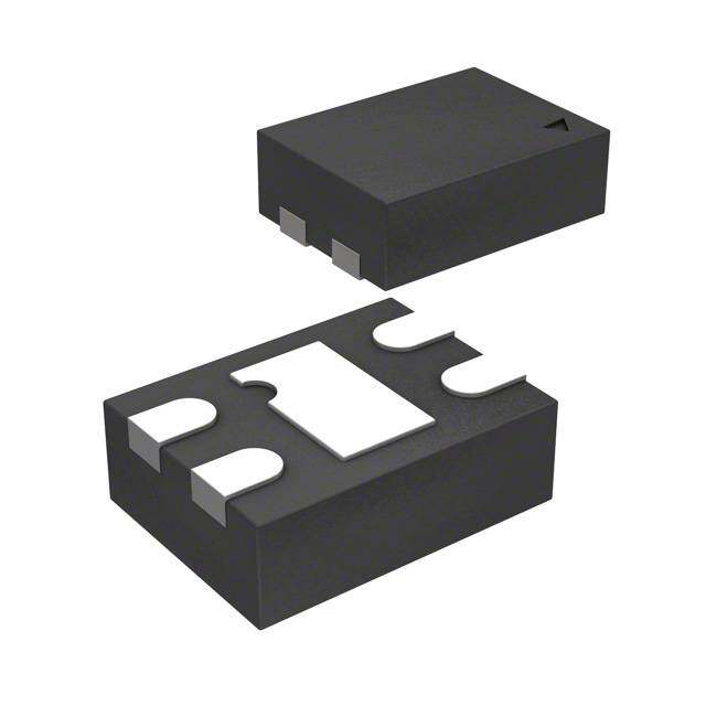
| 产品图片 |
|
| 产品型号 | AOZ1360AIL |
| Rds(On) | 35 毫欧 |
| rohs | 无铅 / 符合限制有害物质指令(RoHS)规范要求 |
| 产品系列 | EZPower™ |
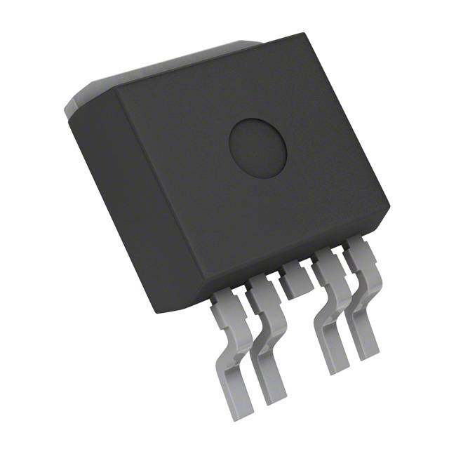
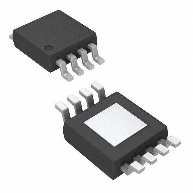
| 供应商器件封装 | 8-SOIC |
| 其它名称 | 785-1418-6 |
| 内部开关 | 是 |
| 包装 | Digi-Reel® |
| 安装类型 | 表面贴装 |
| 封装/外壳 | 8-SOIC(0.154",3.90mm 宽) |
| 工作温度 | -40°C ~ 85°C |
| 标准包装 | 1 |
| 电压-输入 | 5.5 V ~ 28 V |
| 电流限制 | 可调 |
| 类型 | 高端开关 |
| 输出数 | 1 |


- 商务部:美国ITC正式对集成电路等产品启动337调查
- 曝三星4nm工艺存在良率问题 高通将骁龙8 Gen1或转产台积电
- 太阳诱电将投资9.5亿元在常州建新厂生产MLCC 预计2023年完工
- 英特尔发布欧洲新工厂建设计划 深化IDM 2.0 战略
- 台积电先进制程称霸业界 有大客户加持明年业绩稳了
- 达到5530亿美元!SIA预计今年全球半导体销售额将创下新高
- 英特尔拟将自动驾驶子公司Mobileye上市 估值或超500亿美元
- 三星加码芯片和SET,合并消费电子和移动部门,撤换高东真等 CEO
- 三星电子宣布重大人事变动 还合并消费电子和移动部门
- 海关总署:前11个月进口集成电路产品价值2.52万亿元 增长14.8%


PDF Datasheet 数据手册内容提取
AOZ1360 28V Programmable Current-Limited Load Switch General Description Features The AOZ1360 is a member of Alpha and Omega 35m maximum on resistance Semiconductor’s high-side load switch family intended Programmable current limit for applications that require circuit protection. The device 5.5V to 28V operating input voltage operates from a source voltage between 5.5V and 28V. The internal current limiting circuit protects the input Low quiescent current supply voltage from large current load. The current limit Under-voltage lockout can be set with an external resistor. The AOZ1360 Thermal shutdown protection provides thermal protection function that limits excessive 2.5kV ESD rating power dissipation. The device employs internal soft-start circuitry to control in-rush current due to highly capacitive Available in SO-8 or DFN-10 package loads associated with hot-plug events. It features low Applications quiescent current of 220 µA and the supply current reduces to less than 1 µA at shutdown. Notebook PCs Hot swap supplies The AOZ1360 is available in either an SO-8 or a DFN-10 4 mm x 4 mm package which can operate over a -40C to +85C temperature range. Typical Application V V IN OUT IN OUT C1 C2 1μF 1μF AOZ1360 OFF ON EN SET R1 84.5k SS GND C3 1nF Rev. 2.0 January 2015 www.aosmd.com Page 1 of 16
AOZ1360 Ordering Information Part Number Package Temperature Range Environmental AOZ1360AIL SO-8 -40 °C to +85 °C Green Product AOZ1360DIL DFN-10 4x4 AOS Green Products use reduced levels of Halogens, and are also RoHS compliant. Please visit www.aosmd.com/media/AOSGreenPolicy.pdf for additional information. Pin Configuration IN 1 8 OUT IN 1 10 OUT IN 2 7 OUT IN OUT OUT 2 9 GND 3 6 SET NC 3 8 NC GND 4 7 SET SS 4 5 EN SS 5 GND 6 EN SO-8 DFN-10 (Top View) (Top View) Pin Description Pin Number Pin Name SO-8 DFN 4x4 10L Pin Function IN 1, 2 1, 2 P-channel MOSFET source. Connect a 1 µF capacitor from IN to GND. GND 3 4 Ground. SS 4 5 Soft-Start Pin. Connect a capacitor from SS to GND to set the soft-start time. Connect SS to IN to set to the default soft-start time of 100us. EN 5 6 Enable Input. SET 6 7 Current Limit Set Pin. Connect a resistor from SET to GND to set the switch current limit. NC 3, 8 No Connect OUT 7, 8 9, 10 P-channel MOSFET Drain. Connect a capacitor with 0.1 µF or above from OUT to GND. Rev. 2.0 January 2015 www.aosmd.com Page 2 of 16
AOZ1360 Functional Block Diagram IN OUT C1 C2 1μF 1μF 5V Linear Gate Driver & SET Slew Rate Current Limit Regulator Control R1 84.5kΩ 5.5V SS UVLO Comparator C3 Thermal 1nF EN Shutdown AOZ1360 Figure 1. Functional Block Diagram Timing Diagram VIH EN VIL 90% 90% 10% OUT TD(ON) TD(OFF) TR Figure 2. AOZ1360 Timing Diagram Absolute Maximum Ratings Recommended Operating Conditions Exceeding the Absolute Maximum Ratings may damage the The device is not guaranteed to operate beyond the maximum device. Recommended Operating Conditions. Parameter Rating Parameter Rating IN to GND -0.3 V to +30 V Junction Temperature (T ) -40 °C to +125 °C J EN, OUT to GND -0.3 V to VIN + 0.3 V Thermal Resistance SS, SET -0.3 V to +6 V SO-8 (JA) 82 °C/W DFN-10 ( ) Maximum Junction Temperature (T ) +150 °C JA 63 °C/W J ESD Rating (Human Body Model) 2.5 kV Rev. 2.0 January 2015 www.aosmd.com Page 3 of 16
AOZ1360 Electrical Characteristics V = 12V, T = 25°C unless otherwise stated. IN A Symbol Parameter Conditions Min. Typ. Max Units V Input Supply Voltage 5.5 28 V IN V Undervoltage Lockout IN rising 4.9 5.4 V UVLO Threshold V Undervoltage Lockout 400 mV UVHYS Hysteresis I Input Quiescent Current EN = IN, no load 220 400 A IN_ON I Input Shutdown Current EN = GND, no load 1 A IN_OFF I Output Leakage Current EN = GND, no load 1 A LEAK R Switch On Resistance AOZ1360AI V = 12 V 22 35 m DS(ON) IN R Switch On Resistance AOZ1360AI V = 5.5 V 33 43 m DS(ON) IN I Current Limit R = 84.5 k 2 2.7 3.4 A LIM SET V Enable Input Low Voltage 0.8 V EN_L V Enable Input High Voltage 2.0 V EN_H V Enable Input Hysteresis 100 mV EN_HYS I Enable Input Bias Current 1 A EN_BIAS Td_on Turn-On Delay Time R = 120 , C = 1 F, SS = Floated 220 s L L EN_50% to OUT_10% t Turn-On Rise Time R = 120 , C = 1 F, SS = Floated 280 s ON L L OUT_10% to 90% R = 120 , C = 1 F, C = 1 nF 360 L L SS t Turn-Off Fall Time R = 120 , C = 1 F, SS = Floated 280 s OFF L L T Thermal Shutdown Threshold 130 C SD T Thermal Shutdown Hysteresis 30 C SD_HYS Rev. 2.0 January 2015 www.aosmd.com Page 4 of 16
AOZ1360 Typical Performance Characteristics Input Quiescent Current Input Shutdown Current 290 1.0 0.9 270 0.8 A) 250 A) 0.7 μ μ nt ( 230 nt ( 0.6 e e urr 85°C urr 0.5 C C pply 210 2-450°°CC pply 0.4 8255°°CC Su 190 Su 0.3 -40°C 0.2 170 0.1 150 0 5 10 15 20 25 30 5 10 15 20 25 30 VIN (V) VIN (V) Output Leakage Current UVLO Threshold vs. Temperature 1.0 4.8 0.9 VIN = 12V A) 0.8 VIN = 5.5V 4.7 μ Current ( 00..67 d (V) 4.6 RFaislliinngg ge 0.5 hol 4.5 a s k e ea 0.4 hr ut L 0.3 T 4.4 p Out 0.2 4.3 0.1 0 4.2 -50 -30 -10 10 30 50 70 90 -60 -40 -20 0 20 40 60 80 100 120 Temperature (°C) Temperature (°C) RDS(ON) vs. Supply Voltage RDS(ON) vs. Temperature 35 40 30 35 30 25 mΩ) 20 mΩ) 25 VIN = 12V (N) (N) 20 VIN = 5.5V O O S( 15 S( D D 15 R R 10 10 5 5 0 0 -50 -30 -10 10 30 50 70 90 -60 -40 -20 0 20 40 60 80 100 120 VIN (V) Temperature (°C) Rev. 2.0 January 2015 www.aosmd.com Page 5 of 16
AOZ1360 Typical Performance Characteristics (Continued) Enable Input Threshold (Rising) vs. Temperature Enable Input Threshold (Falling) vs. Temperature 1.8 1.8 1.6 VIN = 12V 1.6 VIN = 12V VIN = 5.5V VIN = 5.5V 1.4 1.4 1.2 1.2 V) 1.0 V) 1.0 (N (N VE0.8 VE 0.8 0.6 0.6 0.4 0.4 0.2 0.2 0 0 -60 -40 -20 0 20 40 60 80 100 120 -60 -40 -20 0 20 40 60 80 100 120 Temperature (°C) Temperature (°C) Current Derating Curve for SO8 Current Derating Curve for DFN-10 4x4 7.0 6.5 6.3 6.5 6.1 6.0 5.9 A) 5.5 A) 5.7 ent ( 5.0 ent ( 5.5 Curr 4.5 Curr 5.3 5.1 4.0 4.9 3.5 4.7 3.0 4.5 0 10 20 30 40 50 60 70 80 90 -40 -20 0 20 40 60 80 100 Ambient Temperature (°C) Ambient Temperature (°C) Internal Power MOSFET SOA 100.0 10ms 10.0 RDS(ON) 100m limited s) 1ms mp 1.0 A ( D -I 0.1 TJ(Max)=150(cid:101)C 10s TA=25(cid:101)C DC 0.0 0.01 0.1 1 10 100 -VDS(Volts) Rev. 2.0 January 2015 www.aosmd.com Page 6 of 16
AOZ1360 Typical Performance Characteristics (Continued) Turn-On Turn-Off (V = 12V, R = 5.6Ω) (V = 12V, R = 5.6Ω) IN IN VIN VIN 2V/div 2V/div VOUT VOUT 2V/div 2V/div EN EN 1V/div 1V/div IOUT IOUT 0.5A/div 0.5A/div 1ms/div 20μs/div Current Limit Over Temperature (V = 12V, R = 3.6Ω) (V = 12V, R = 3.6Ω) IN IN V V IN IN 5V/div 2V/div VOUT VOUT 2V/div 2V/div EN EN 1V/div 1V/div IOUT IOUT 0.5A/div 0.5A/div 5ms/div 100ms/div Rev. 2.0 January 2015 www.aosmd.com Page 7 of 16
AOZ1360 Detailed Description Introduction The slew rate rise time, Ton, can be set using the following equation: The AOZ1360 is a 35 m P-channel high-side load switch with adjustable soft-start slew-rate control, CssV programmable current limit and thermal shutdown. Ton = ----------------------I--N-- 30A It operates with an input voltage range from 5.5 V to 28 V. Enable Programmable Current Limit The EN pin is the On/Off control for the output switch. The current limit is programmed by an external resistor It is an active-high input. The EN pin is active after V is connected between the SET pin and ground. This sets a IN above the UVLO threshold of 4.9 V. Conversely, the reference voltage to the current limit error amplifier that EN pin will be deactivated if the V falls below the UVLO compares it to a sensed voltage that is generated by IN of 2.0V. The EN pin must be driven to a logic high or logic passing a small portion of the load current through an low state to guarantee operation. While disabled, the internal amplifier. When the sensed load current exceeds AOZ1360 only draws approximately 1 µA supply current. the set current limit, the load current is then clamped at The EN is a high impedance input with an ESD protection the set limit and the Vout drops to whatever voltage is diode to ground and should not be forced below ground. necessary to clamp the load current. The AOZ1360 will This input level is compatible with most microcontroller stay in this condition until the load current no longer outputs and other logic families. exceeds the current limit or if the thermal shutdown protection is engaged. Under-Voltage Lockout (UVLO) The under-voltage lockout (UVLO) circuit of the Thermal-Shutdown Protection AOZ1360 monitors the input voltage and prevents the During current limit or short circuit conditions, the PMOS output MOSFET from turning on until V exceeds 4.9 V. resistance is increased to clamp the load current. This IN increases the power dissipation in the chip causing the Adjustable Soft-Start Slew-Rate Control die temperature to rise. When the die temperature When the EN pin is high, the slew rate control circuitry reaches 130 °C the thermal shutdown circuitry will applies voltage on the gate of the PMOS switch in a shutdown the device. There is a 30 °C hysteresis after manner such that the output voltage and current is which the device will turn back on and go through soft ramped up linearly until it reaches the steady-state load start. The thermal shutdown will cycle repeatedly until the current level. The slew rate can be adjusted by an short circuit condition is resolved or the enable pin is external capacitor connected between the SS pin pulled LOW externally. and ground. Rev. 2.0 January 2015 www.aosmd.com Page 8 of 16
AOZ1360 Application Information Input Capacitor Selection Slew Rate Setting The input capacitor prevents large voltage transients Slew rate is set by changing the capacitor value on the from appearing at the input and provides the SS pin of the device. A capacitor connected between the instantaneous current needed each time the switch SS pin and ground will reduce the output slew-rate. The turns on. The input capacitor also limits input voltage capacitive range is 0.001 µF to 0.1 µF. Refer to Figure 4. drop and prevents high-frequency noise on the power 45 line from passing through the output of the power side. 40 The choice of input capacitor is based on its ripple current and voltage ratings rather than the actual 35 capacitance value. The input capacitor should be located 30 as close to VIN as possible. A 1 µF ceramic cap is Slew Rate 25 recommended. However, higher capacitor values will (ms) further reduce the voltage drop at the input. 20 15 Output Capacitor Selection 10 The output capacitor acts in a similar way. A small 0.1 µF 5 capacitor prevents high-frequency noise from going into the system. Also, the output capacitor has to supply 0 0 0.02 0.04 0.06 0.08 0.1 enough current for any large load that may occur during system transients. This bulk capacitor must be large Capacitance (μF) enough to supply fast transient load in order to Figure 4. Output Slew Rate Adjustment vs. Capacitance prevent the output from dropping. Current Limit Setting The current limit is set by an external resistor connected Power Dissipation Calculation to the SET pin. Refer to Figure 3 for current limit settings. Calculate the power dissipation for normal load condition using the following equation: AOZ1360 Rset vs ILIM P = R x (I )2 D ON OUT 7 The worst case power dissipation occurs when the 6 load current hits the current limit due to over-current or short circuit faults. The power dissipation under these 5 conditions can be calculated using the following 4 equation: ILIM (A) 3 P = (V – V ) x I D IN OUT LIMIT 2 1 0 35 45 55 65 75 85 95 105 RSET (kΩ) Figure 3 Rev. 2.0 January 2015 www.aosmd.com Page 9 of 16
AOZ1360 Layout Guidelines Proper PCB layout is important for improving the thermal Place the input and output bypass capacitors as close as and overall performance of the AOZ1360. To optimize the possible to the IN and OUT pins. The input and output switch response time for outputting short-circuit PCB traces should be as wide as possible for the given conditions, keep all traces as short as possible. This will PCB space. Use a ground plane to enhance the power also reduce the effect of unwanted parasitic inductance. dissipation capability of the device. IN 1 10 OUT IN 1 8 OUT OUT IN 2 9 OUT IN 2 7 OUT NC 3 8 NC C1 C1 GND 3 6 SET C2 GND 4 7 SET C2 GGNNDD SS 4 5 EN R1 SS 5 6 EN R1 C3 C3 GND Figure 5. AOZ1360AI (SO-8) Layout Figure 6. AOZ1360DI (DFN4x4 10L) Layout Rev. 2.0 January 2015 www.aosmd.com Page 10 of 16
AOZ1360 Package Dimensions, SO-8L D Gauge Plane Seating Plane e 0.25 8 L E1 E h x 45 1 C θ 7 (4x) A2 A 0.1 b A1 RECOMMENDED LAND PATTERN Dimensions in millimeters Dimensions in inches Symbols Min. Nom. Max. Symbols Min. Nom. Max. A 1.35 1.65 1.75 A 0.053 0.065 0.069 2.20 A1 0.10 — 0.25 A1 0.004 — 0.010 A2 1.25 1.50 1.65 A2 0.049 0.059 0.065 b 0.31 — 0.51 b 0.012 — 0.020 c 0.17 — 0.25 c 0.007 — 0.010 D 4.80 4.90 5.00 D 0.189 0.193 0.197 5.74 E 3.80 3.90 4.00 E 0.150 0.154 0.157 e 1.27 BSC e 0.050 BSC 2.87 1.27 E1 5.80 6.00 6.20 E1 0.228 0.236 0.244 h 0.25 — 0.50 h 0.010 — 0.020 L 0.40 — 1.27 L 0.016 — 0.050 θ 0° — 8° θ 0° — 8° 0.80 0.635 UNIT: mm Notes: 1. All dimensions are in millimeters. 2. Dimensions are inclusive of plating 3. Package body sizes exclude mold flash and gate burrs. Mold flash at the non-lead sides should be less than 6 mils. 4. Dimension L is measured in gauge plane. 5. Controlling dimension is millimeter, converted inch dimensions are not necessarily exact. Rev. 2.0 January 2015 www.aosmd.com Page 11 of 16
AOZ1360 Tape and Reel Dimensions, SO-8 Carrier Tape P1 D1 P2 T E1 E2 E B0 K0 D0 A0 P0 Feeding Direction UNIT: mm Package A0 B0 K0 D0 D1 E E1 E2 P0 P1 P2 T SO-8 6.40 5.20 2.10 1.60 1.50 12.00 1.75 5.50 8.00 4.00 2.00 0.25 (12mm) ±0.10 ±0.10 ±0.10 ±0.10 ±0.10 ±0.10 ±0.10 ±0.10 ±0.10 ±0.10 ±0.10 ±0.10 Reel W1 S G N M K V R H W UNIT: mm Tape Size Reel Size M N W W1 H K S G R V 12mm ø330 ø330.00 ø97.00 13.00 17.40 ø13.00 10.60 2.00 — — — ±0.50 ±0.10 ±0.30 ±1.00 +0.50/-0.20 ±0.50 Leader/Trailer and Orientation Trailer Tape Components Tape Leader Tape 300mm min. or Orientation in Pocket 500mm min. or 75 empty pockets 125 empty pockets Rev. 2.0 January 2015 www.aosmd.com Page 12 of 16
AOZ1360 Package Dimensions, DFN-10L, 4x4 D A 3 B e * INDEX AREA D/2 6 10 L3 (D/2xE/2) L D/2 *L4 L1 E1/2 E E1 L2 2 Pin #1 IDA Pin 1 *L4 5 1 Chamfer 0.20 D2 D1 6 TOP VIEW BOTTOM VIEW A3 A1 C A Seating Plane 10x 5 ddd b 4 SIDE VIEW eee Dimensions in millimeters Dimensions in inches Symbols Min. Nom. Max. Symbols Min. Nom. Max. A 0.70 0.75 0.80 A 0.028 0.030 0.031 RECOMMENDED LAND PATTERN A1 0.00 0.02 0.05 A1 0.000 0.001 0.002 0.65 Typ. A3 0.203 REF A3 0.008 REF 0.65 Typ. b 0.30 0.35 0.40 b 0.012 0.014 0.016 0.35 TYP D 3.95 4.00 4.05 D 0.156 0.157 0.159 10 6 0.30 D1 1.58 1.68 1.78 D1 0.062 0.066 0.070 D2 1.22 1.32 1.42 D2 0.048 0.052 0.056 E 3.95 4.00 4.05 E 0.156 0.157 0.159 E1 2.20 2.30 2.40 E1 0.087 0.091 0.094 0.38 2.30 3.55 e 0.65 BSC e 0.026 BSC 1.15 L 0.50 0.55 0.60 L 0.020 0.022 0.024 0.02 L1 — 0.02 0.12 L1 — 0.001 0.005 L2 0.28 0.38 0.48 L2 0.011 0.015 0.019 L3 0.85 REF L3 0.033 REF. Pin #1 IDA Chamfer 0.20 1 5 0.30 L4 0.30 REF L4 0.012 REF 1.78 1.42 aaa 0.15 aaa 0.006 Unit: mm bbb 0.10 bbb 0.004 ccc 0.10 ccc 0.004 ddd 0.08 ddd 0.003 Notes: eee 0.05 eee 0.002 1. All dimensions are in millimeters. 2. The dimensions with * are just for reference. 3. The location of the terminal #1 identifier and terminal numbering convention conforms to JEDEC publication 95 SPP-002. 4. Dimension b applies to metallized terminal and is measured between 0.15mm and 0.30mm from the terminal tip. If the terminal has the optional radius on the other end of the terminal, then dimension b should not be measured in that radius area. 5. Coplanarity applies to the terminals and all other bottom surface metallization. 6. Drawings shown are for illustration only. Rev. 2.0 January 2015 www.aosmd.com Page 13 of 16
AOZ1360 Tape and Reel Dimensions, DFN-10L, 4x4 Carrier Tape D1 P1 P2 T E1 E2 E CL B0 K0 P0 D0 A0 Feeding Direction UNIT: MM Package A0 B0 K0 D0 D1 E E1 E2 P0 P1 P2 T DFN 4x4 4.35 4.35 1.10 1.50 1.50 12.0 1.75 5.50 8.00 4.00 2.00 0.30 (12mm) ±0.10 ±0.10 ±0.10 Min. +0.1/-0.0 ±0.3 ±0.10 ±0.05 ±0.10 ±0.10 ±0.05 ±0.05 Reel W1 S G N M K V R H W UNIT: MM Tape Size Reel Size M N W W1 H K S G R V 12 mm ø330 ø330.0 ø79.0 12.4 17.0 ø13.0 10.5 2.0 — — — ±2.0 ±1.0 +2.0/-0.0 +2.6/-0.0 ±0.5 ±0.2 ±0.5 Leader/Trailer and Orientation Trailer Tape Components Tape Leader Tape 300mm min. or Orientation in Pocket 500mm min. or 75 empty pockets 125 empty pockets Rev. 2.0 January 2015 www.aosmd.com Page 14 of 16
AOZ1360 Part Marking SO-8 Z1360AI Underscore Indicates Part Number Code Green Product FAYWLT Fab & Assembly Location Assembly Lot Code Year & Week Code DFN-10 Z1360DI Underscore Indicates Part Number Code Green Product ZA8R1B Fab & Assembly Location Assembly Lot Code Year & Week Code Rev. 2.0 January 2015 www.aosmd.com Page 15 of 16
AOZ1360 LEGAL DISCLAIMER Alpha and Omega Semiconductor makes no representations or warranties with respect to the accuracy or completeness of the information provided herein and takes no liabilities for the consequences of use of such information or any product described herein.Alpha and Omega Semiconductor reserves the right to make changes to such information at any time without further notice. This document does not constitute the grant of any intellectual property rights or representation of non-infringement of any third party’s intellectual property rights. LIFE SUPPORT POLICY ALPHA AND OMEGA SEMICONDUCTOR PRODUCTS ARE NOT AUTHORIZED FOR USE AS CRITICAL COMPONENTS IN LIFE SUPPORT DEVICES OR SYSTEMS. As used herein: 1. Life support devices or systems are devices or 2. A critical component in any component of a life systems which, (a) are intended for surgical implant into support, device, or system whose failure to perform can the body or (b) support or sustain life, and (c) whose be reasonably expected to cause the failure of the life failure to perform when properly used in accordance support device or system, or to affect its safety or with instructions for use provided in the labeling, can be effectiveness. reasonably expected to result in a significant injury of the user. Rev. 2.0 January 2015 www.aosmd.com Page 16 of 16