ICGOO在线商城 > 集成电路(IC) > 数据采集 - 数模转换器 > ADV7123JSTZ240

 Datasheet下载
- 型号: ADV7123JSTZ240
- 制造商: Analog
- 库位|库存: xxxx|xxxx
- 要求:
| 数量阶梯 | 香港交货 | 国内含税 |
| +xxxx | $xxxx | ¥xxxx |
查看当月历史价格
查看今年历史价格
ADV7123JSTZ240产品简介:
ICGOO电子元器件商城为您提供ADV7123JSTZ240由Analog设计生产,在icgoo商城现货销售,并且可以通过原厂、代理商等渠道进行代购。 ADV7123JSTZ240价格参考¥81.89-¥104.16。AnalogADV7123JSTZ240封装/规格:数据采集 - 数模转换器, 10 位 数模转换器 3 48-LQFP(7x7)。您可以下载ADV7123JSTZ240参考资料、Datasheet数据手册功能说明书,资料中有ADV7123JSTZ240 详细功能的应用电路图电压和使用方法及教程。
Analog Devices Inc.(ADI)的ADV7123JSTZ240是一款高性能、三通道、10位数模转换器(DAC),广泛应用于需要高速、高精度模拟信号输出的场合。以下是该型号的主要应用场景:

 1. 视频处理与显示
   ADV7123JSTZ240在视频处理领域有广泛应用,尤其适用于需要高质量RGB或YCbCr视频信号输出的设备。它能够提供高达330 MHz的像素时钟频率,支持标准和非标准的视频格式,如VGA、SVGA、XGA、SXGA等。其三通道设计可以分别处理红、绿、蓝(RGB)信号,确保图像色彩的准确性和清晰度。

 2. 测试与测量设备
   在测试与测量仪器中,ADV7123JSTZ240用于生成精确的模拟波形,如正弦波、方波、三角波等。它的高分辨率和快速响应特性使其适合用于示波器、信号发生器、频谱分析仪等设备中,帮助工程师进行精确的信号分析和调试。

 3. 通信系统
   该器件在通信系统中也有重要应用,特别是在基带信号处理和调制解调器中。它可以将数字基带信号转换为模拟信号,用于发送端的信号发射,或者在接收端将接收到的模拟信号转换回数字形式进行进一步处理。其低延迟和高线性度特性有助于提高通信系统的性能和可靠性。

 4. 医疗成像
   在医疗成像设备中,ADV7123JSTZ240用于将数字图像数据转换为模拟信号,驱动显示器或其他成像组件。例如,在超声、CT扫描仪、MRI等设备中,它能够确保图像的高分辨率和实时性,帮助医生更准确地诊断病情。

 5. 工业自动化与控制
   在工业自动化领域,ADV7123JSTZ240可用于控制系统中的信号调理和反馈机制。它能够将传感器采集到的数字信号转换为模拟信号,驱动执行器或电机,实现精确的闭环控制。此外,它还适用于各种工业级数据采集系统,确保数据传输的稳定性和准确性。

 6. 音频处理
   尽管主要用于视频和通信,ADV7123JSTZ240也可用于高端音频设备中,如专业音响系统、录音设备等。其高保真度和低失真特性能够确保音频信号的质量,提供更加逼真的听觉体验。

总之,ADV7123JSTZ240凭借其高性能和多功能性,适用于多种需要高速、高精度数模转换的应用场景。
| 参数 | 数值 |
| 产品目录 | 集成电路 (IC)半导体 |
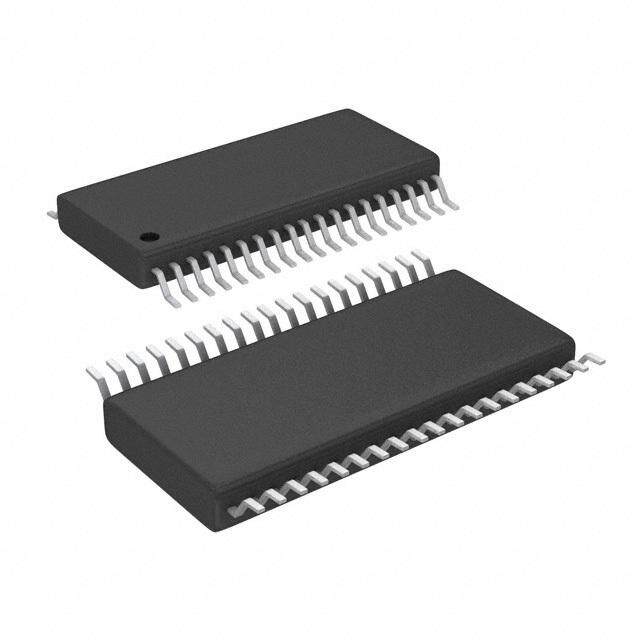
| 描述 | IC DAC VIDEO TRPL HI SPD 48-LQFP视频 IC 330MHz Triple 10B High Speed DAC |
| 产品分类 | |
| 品牌 | Analog Devices |
| 产品手册 | |
| 产品图片 |
|
| rohs | 符合RoHS无铅 / 符合限制有害物质指令(RoHS)规范要求 |
| 产品系列 | 多媒体 IC,视频 IC,Analog Devices ADV7123JSTZ240- |
| 数据手册 | |
| 产品型号 | ADV7123JSTZ240 |
| 产品培训模块 | http://www.digikey.cn/PTM/IndividualPTM.page?site=cn&lang=zhs&ptm=19145http://www.digikey.cn/PTM/IndividualPTM.page?site=cn&lang=zhs&ptm=18614http://www.digikey.cn/PTM/IndividualPTM.page?site=cn&lang=zhs&ptm=26125http://www.digikey.cn/PTM/IndividualPTM.page?site=cn&lang=zhs&ptm=26140http://www.digikey.cn/PTM/IndividualPTM.page?site=cn&lang=zhs&ptm=26150http://www.digikey.cn/PTM/IndividualPTM.page?site=cn&lang=zhs&ptm=26147 |
| 产品目录页面 | |
| 产品种类 | 视频 IC |
| 位数 | 10 |
| 供应商器件封装 | 48-LQFP(7x7) |
| 分辨率 | 10 bit |
| 包装 | 托盘 |
| 商标 | Analog Devices |
| 安装类型 | 表面贴装 |
| 安装风格 | SMD/SMT |
| 封装 | Tray |
| 封装/外壳 | 48-LQFP |
| 封装/箱体 | LQFP-48 |
| 工作温度 | 0°C ~ 70°C |
| 工作电源电压 | 3 V to 5.25 V |
| 工厂包装数量 | 250 |
| 建立时间 | - |
| 数据接口 | 并联 |
| 最大功率耗散 | 485 mW |
| 最大工作温度 | + 85 C |
| 最小工作温度 | - 40 C |
| 标准包装 | 1 |
| 电压源 | 单电源 |
| 类型 | Video Encoder |
| 系列 | ADV7123 |
| 转换器数 | 3 |
| 输出数和类型 | 6 电流,单极 |
| 通道数量 | 3 Channel |
| 采样率(每秒) | 240M |


- 商务部:美国ITC正式对集成电路等产品启动337调查
- 曝三星4nm工艺存在良率问题 高通将骁龙8 Gen1或转产台积电
- 太阳诱电将投资9.5亿元在常州建新厂生产MLCC 预计2023年完工
- 英特尔发布欧洲新工厂建设计划 深化IDM 2.0 战略
- 台积电先进制程称霸业界 有大客户加持明年业绩稳了
- 达到5530亿美元!SIA预计今年全球半导体销售额将创下新高
- 英特尔拟将自动驾驶子公司Mobileye上市 估值或超500亿美元
- 三星加码芯片和SET,合并消费电子和移动部门,撤换高东真等 CEO
- 三星电子宣布重大人事变动 还合并消费电子和移动部门
- 海关总署:前11个月进口集成电路产品价值2.52万亿元 增长14.8%


PDF Datasheet 数据手册内容提取
CMOS, 170 MHz, Triple, 10-Bit High Speed Video DAC Enhanced Product ADV7123-EP FEATURES FUNCTIONAL BLOCK DIAGRAM 170 MSPS throughput rate VAA Triple, 10-bit digital-to-analog converters (DACs) SFDR BLANK BLANKAND SYNC LOGIC −70 dB at f = 50 MHz; f = 1 MHz SYNC CLK OUT −53 dB at fCLK = 140 MHz; fOUT = 40 MHz DATA IOR RS-343A-/RS-170-compatible output R9TO R0 10 REGISTER 10 DAC IOR Complementary outputs DATA IOG DAC output current range: 2.0 mA to 26.5 mA G9TO G0 10 REGISTER 10 DAC IOG TTL-compatible inputs Internal reference: 1.235 V DATA IOB B9TO B0 10 REGISTER 10 DAC Single-supply 3.3 V operation IOB 48-lead LFCSP package POWER-DOWN VOLTAGE Low power dissipation: 30 mW minimum at 3 V PSAVE MODE REFERENCE VREF CIRCUIT Low power standby mode: 6 mW typical at 3 V CLOCK ADV7123-EP ENHANCED PRODUCT FEATURES GND RSET COMP 09200-001 Supports defense and aerospace applications Figure 1. (AQEC standard) Military temperature range: −55°C to +105°C GENERAL DESCRIPTION Controlled manufacturing baseline One assembly/test site The ADV7123-EP is a triple, high speed digital-to-analog One fabrication site converter (DAC) on a single monolithic chip. It consists of three Product change notification high speed, 10-bit video DACs with complementary outputs, Qualification data available on request a standard TTL input interface, and a high impedance, analog APPLICATIONS output current source. Digital video systems The ADV7123-EP has three separate 10-bit-wide input ports. High resolution color graphics A single 3.3 V power supply and clock are the only components Digital radio modulation required to make the part functional. The ADV7123-EP has Image processing additional video control signals: composite SYNC and BLANK. Instrumentation The ADV7123-EP also has a power save mode. Video signal reconstruction The ADV7123-EP is fabricated in a 5 V CMOS process. Its monolithic CMOS construction ensures greater functionality with lower power dissipation. The ADV7123-EP is available in a 48-lead LFCSP package. Full details about this enhanced product are available in the ADV7123 data sheet, which should be consulted in conjunction with this data sheet. PRODUCT HIGHLIGHTS 1. Guaranteed monotonic to 10 bits. 2. Compatible with a wide variety of high resolution color graphics systems, including RS-343A and RS-170. Rev. A Document Feedback Information furnished by Analog Devices is believed to be accurate and reliable. However, no responsibility is assumed by Analog Devices for its use, nor for any infringements of patents or other One Technology Way, P.O. Box 9106, Norwood, MA 02062-9106, U.S.A. rights of third parties that may result from its use. Specifications subject to change without notice. No license is granted by implication or otherwise under any patent or patent rights of Analog Devices. Tel: 781.329.4700 ©2010-2018 Analog Devices, Inc. All rights reserved. Trademarks and registered trademarks are the property of their respective owners. Technical Support www.analog.com
ADV7123-EP Enhanced Product TABLE OF CONTENTS Features .............................................................................................. 1 Dynamic Specifications ................................................................4 Enhanced Product Features ............................................................ 1 Timing Specifications ...................................................................5 Applications ....................................................................................... 1 Absolute Maximum Ratings ............................................................7 Functional Block Diagram .............................................................. 1 ESD Caution...................................................................................7 General Description ......................................................................... 1 Pin Configuration and Function Descriptions ..............................8 Product Highlights ........................................................................... 1 Outline Dimensions ....................................................................... 10 Revision History ............................................................................... 2 Ordering Guide .......................................................................... 10 Specifications ..................................................................................... 3 REVISION HISTORY 5/2018—Rev. 0 to Rev. A Changes to Features Section............................................................ 1 Added Enhanced Product Features Section .................................. 1 Updated Outline Dimensions ....................................................... 10 Changes to Ordering Guide .......................................................... 10 7/2010—Revision 0: Initial Version Rev. A | Page 2 of 10
Enhanced Product ADV7123-EP SPECIFICATIONS V = 3.0 V to 3.6 V, V = 1.235 V, R = 560 Ω, C = 10 pF. All specifications T to T ,1 unless otherwise noted; T = 110°C. AA REF SET L MIN MAX J MAX Table 1. Parameter2 Min Typ Max Unit Test Conditions/Comments1 STATIC PERFORMANCE Resolution (Each DAC) 10 Bits R = 680 Ω SET Integral Nonlinearity (BSL) −1 +0.5 +1 LSB R = 680 Ω SET Differential Nonlinearity −1 +0.25 +1 LSB R = 680 Ω SET DIGITAL AND CONTROL INPUTS Input High Voltage, V 2.0 V IH Input Low Voltage, V 0.8 V IL Input Current, I −1 +1 μA V = 0.0 V or V IN IN DD PSAVE Pull-Up Current 20 μA Input Capacitance, C 10 pF IN ANALOG OUTPUTS Output Current 2.0 26.5 mA Green DAC, SYNC = high 2.0 18.5 mA RGB DAC, SYNC = low DAC-to-DAC Matching 1.0 % Output Compliance Range, V 0 1.4 V OC Output Impedance, R 70 kΩ OUT Output Capacitance, C 10 pF OUT Offset Error 0 0 % FSR Tested with DAC output = 0 V Gain Error3 0 % FSR FSR = 17.62 mA VOLTAGE REFERENCE, EXTERNAL Reference Range, V 1.12 1.235 1.35 V REF VOLTAGE REFERENCE, INTERNAL Voltage Reference, V 1.235 V REF POWER DISSIPATION Digital Supply Current4 2.2 5.0 mA f = 50 MHz CLK 6.5 12.0 mA f = 140 MHz CLK 7.5 13.5 mA f = 170 MHz CLK Analog Supply Current 67 72 mA R = 560 Ω SET 8 mA R = 4933 Ω SET Standby Supply Current 2.1 5.0 mA PSAVE = low, digital and control inputs at VDD Power Supply Rejection Ratio 0.1 0.5 %/% 1 Temperature range TMIN to TMAX: −55°C to +105°C. 2 These maximum/minimum specifications are guaranteed by characterization over the 3.0 V to 3.6 V range. 3 Gain error = {(Measured (FSC)/Ideal (FSC) − 1) × 100}, where Ideal (FSC) = VREF/RSET × K × (0x3FFH) and K = 7.9896. 4 Digital supply is measured with a continuous clock that has data input corresponding to a ramp pattern and with an input level at 0 V and VDD. Rev. A | Page 3 of 10
ADV7123-EP Enhanced Product DYNAMIC SPECIFICATIONS V = 3.0 V to 3.6 V, V = 1.235 V, R = 680 Ω, C = 10 pF. All specifications are at T = 25°C, unless otherwise noted; T = 110°C. AA REF SET L A J MAX Table 2. Parameter1 Min Typ Max Unit AC LINEARITY Spurious-Free Dynamic Range to Nyquist2 Single-Ended Output f = 50 MHz; f = 1.00 MHz 67 dBc CLK OUT f = 50 MHz; f = 2.51 MHz 67 dBc CLK OUT f = 50 MHz; f = 5.04 MHz 63 dBc CLK OUT f = 50 MHz; f = 20.2 MHz 55 dBc CLK OUT f = 100 MHz; f = 2.51 MHz 62 dBc CLK OUT f = 100 MHz; f = 5.04 MHz 60 dBc CLK OUT f = 100 MHz; f = 20.2 MHz 54 dBc CLK OUT f = 100 MHz; f = 40.4 MHz 48 dBc CLK OUT f = 140 MHz; f = 2.51 MHz 57 dBc CLK OUT f = 140 MHz; f = 5.04 MHz 58 dBc CLK OUT f = 140 MHz; f = 20.2 MHz 52 dBc CLK OUT f = 140 MHz; f = 40.4 MHz 41 dBc CLK OUT Double-Ended Output f = 50 MHz; f = 1.00 MHz 70 dBc CLK OUT f = 50 MHz; f = 2.51 MHz 70 dBc CLK OUT f = 50 MHz; f = 5.04 MHz 65 dBc CLK OUT f = 50 MHz; f = 20.2 MHz 54 dBc CLK OUT f = 100 MHz; f = 2.51 MHz 67 dBc CLK OUT f = 100 MHz; f = 5.04 MHz 63 dBc CLK OUT f = 100 MHz; f = 20.2 MHz 58 dBc CLK OUT f = 100 MHz; f = 40.4 MHz 52 dBc CLK OUT f = 140 MHz; f = 2.51 MHz 62 dBc CLK OUT f = 140 MHz; f = 5.04 MHz 61 dBc CLK OUT f = 140 MHz; f = 20.2 MHz 55 dBc CLK OUT f = 140 MHz; f = 40.4 MHz 53 dBc CLK OUT Spurious-Free Dynamic Range Within a Window Single-Ended Output f = 50 MHz; f = 1.00 MHz; 1 MHz Span 77 dBc CLK OUT f = 50 MHz; f = 5.04 MHz; 2 MHz Span 73 dBc CLK OUT f = 140 MHz; f = 5.04 MHz; 4 MHz Span 64 dBc CLK OUT Double-Ended Output f = 50 MHz; f = 1.00 MHz; 1 MHz Span 74 dBc CLK OUT f = 50 MHz; f = 5.00 MHz; 2 MHz Span 73 dBc CLK OUT f = 140 MHz; f = 5.00 MHz; 4 MHz Span 60 dBc CLK OUT Total Harmonic Distortion f = 50 MHz; f = 1.00 MHz CLK OUT T = 25°C 66 dBc A T to T 65 dBc MIN MAX f = 50 MHz; f = 2.00 MHz 64 dBc CLK OUT f = 100 MHz; f = 2.00 MHz 64 dBc CLK OUT f = 140 MHz; f = 2.00 MHz 55 dBc CLK OUT Rev. A | Page 4 of 10
Enhanced Product ADV7123-EP Parameter1 Min Typ Max Unit DAC PERFORMANCE Glitch Impulse 10 pV-sec DAC-to-DAC Crosstalk3 23 dB Data Feedthrough4, 5 22 dB Clock Feedthrough4, 5 33 dB 1 These maximum/minimum specifications are guaranteed by characterization over the 3.0 V to 3.6 V range. 2 The ADV7123-EP exhibits high performance when operating with an internal voltage reference, VREF. 3 DAC-to-DAC crosstalk is measured by holding one DAC high while the other two DACs are making low-to-high and high-to-low transitions. 4 Clock and data feedthrough is a function of the amount of overshoot and undershoot on the digital inputs. Glitch impulse includes clock and data feedthrough. 5 TTL input values are 0 V to 3 V, with input rise/fall times of 3 ns, measured at the 10% and 90% points. Timing reference points are 50% for inputs and outputs. TIMING SPECIFICATIONS V = 3.0 V to 3.6 V, V = 1.235 V, R = 560 Ω, C = 10 pF. All specifications T to T ,1 unless otherwise noted; T = 110°C. AA REF SET L MIN MAX J MAX Table 3. Parameter2, 3 Symbol Min Typ Max Unit Test Conditions/Comments ANALOG OUTPUTS Analog Output Delay t 7.5 ns 6 Analog Output Rise/Fall Time4 t 1.0 ns 7 Analog Output Transition Time5 t 15 ns 8 Analog Output Skew6 t 1 2 ns 9 CLOCK CONTROL CLOCK Frequency7 f 170 MHz CLK Data and Control Setup t 0.68 ns 1 Data and Control Hold t 2.9 ns 2 CLOCK Period t 5.88 ns 3 CLOCK Pulse Width High6 t 2.6 ns f = 170 MHz 4 CLK_MAX CLOCK Pulse Width Low6 t 2.6 ns f = 170 MHz 5 CLK_MAX Pipeline Delay6 t 1.0 1.0 1.0 Clock cycles PD PSAVE Up Time6 t10 4 10 ns 1 Temperature range TMIN to TMAX: −55°C to +105°C. 2 These maximum/minimum specifications are guaranteed by characterization over the 3.0 V to 3.6 V range. 3 Timing specifications are measured with input levels of 3.0 V (VIH) and 0 V (VIL). 4 Rise time was measured from the 10% to 90% point of zero to full-scale transition, fall time from the 90% to 10% point of a full-scale transition. 5 Measured from the 50% point of full-scale transition to within 2% of the final output value. 6 Guaranteed by characterization. 7 fCLK maximum specification production tested at 125 MHz. Rev. A | Page 5 of 10
ADV7123-EP Enhanced Product t3 t4 t5 CLOCK t2 DIGITAL INPUTS (R9TO R0, G9TO G0, B9TO B0, SYNC, BLANK) t1 t6 t8 ANALOG INPUTS (IOR, IOR, IOG, IOG, IOB, IOB) t7 NOTES 1. OUTPUT DELAY (t6) MEASURED FROM THE 50% POINT OF THE RISING EDGE OF CLOCKTO THE 50% POINT OF FULL-SCALE TRANSITION. 32.. TOFRIUNATANPLSU OITTU IROTIPNSUE TT/FIMAVEAL LL(t UT8E)I MM.EE A(tS7)U MREEADS FURROEMD TBHEET W50E%E NP OTIHNET 1O0F% FAUNLDL -9S0C%A PLEO ITNRTASN OSFIT FIOUNLLT-OS CWAILTEH ITNR 2A%N SOIFT ITOHNE. 09200-002 Figure 2. Timing Diagram Rev. A | Page 6 of 10
Enhanced Product ADV7123-EP ABSOLUTE MAXIMUM RATINGS Table 4. Stresses at or above those listed under Absolute Maximum Parameter Rating Ratings may cause permanent damage to the product. This is a V to GND 7 V stress rating only; functional operation of the product at these AA Voltage on Any Digital Pin GND − 0.5 V to V + 0.5 V or any other conditions above those indicated in the operational AA Ambient Operating Temperature (T ) −55°C to +105°C section of this specification is not implied. Operation beyond A Storage Temperature (T) −65°C to +150°C the maximum operating conditions for extended periods may S Junction Temperature (T) 150°C affect product reliability. J Lead Temperature (Soldering, 10 sec) 300°C ESD CAUTION Vapor Phase Soldering (1 Minute) 220°C I to GND1 0 V to V OUT AA 1 Analog output short circuit to any power supply or common GND can be of an indefinite duration. Rev. A | Page 7 of 10
ADV7123-EP Enhanced Product PIN CONFIGURATION AND FUNCTION DESCRIPTIONS E 9876543210SAV SET RRRRRRRRRRPR 876543210987 444444444333 G0 1 PIN 1 36 VREF G1 2 INDICATOR 35 COMP G2 3 34 IOR G3 4 33 IOR G4 5 32 IOG G5 6 ADV7123-EP 31 IOG G6 7 TOP VIEW 30 VAA G7 8 (Not to Scale) 29 VAA G8 9 28 IOB G910 27 IOB BLANK 11 26 GND SYNC12 25 GND 131415161718192021222324 VAAB0B1B2B3B4B5B6B7B8B9CLOCK 09200-003 NOTES 1. THE EXPOSED PADDLE ON THE UNDERSIDE OF THE PACKAGE MUST BE SOLDERED TO THE GROUND PLANE TO INCREASE THE RELIABILITY OF THE SOLDER JOINTS AND TO MAXIMIZE THE THERMAL CAPABILITY OF THE PACKAGE. Figure 3. Pin Configuration Table 5. Pin Function Descriptions Pin No. Mnemonic Description 1 to 10, G0 to G9, Red, Green, and Blue Pixel Data Inputs (TTL Compatible). Pixel data is latched on the rising edge of CLOCK. 14 to 23, B0 to B9, R0, G0, and B0 are the least significant data bits. Unused pixel data inputs should be connected to either the 39 to 48 R0 to R9 regular printed circuit board (PCB) power or ground plane. 11 BLANK Composite Blank Control Input (TTL Compatible). A Logic 0 on this control input drives the analog outputs— IOR, IOB, and IOG—to the blanking level. The BLANK signal is latched on the rising edge of CLOCK. When BLANK is a Logic 0, the R0 to R9, G0 to G9, and B0 to B9 pixel inputs are ignored. 12 SYNC Composite Sync Control Input (TTL Compatible). A Logic 0 on the SYNC input switches off a 40 IRE current source. The sync current is internally connected to the IOG analog output. SYNC does not override any other control or data input; therefore, it should only be asserted during the blanking interval. SYNC is latched on the rising edge of CLOCK. If sync information is not required on the green channel, the SYNC input should be tied to Logic 0. 13, 29, 30 V Analog Power Supply (3.3 V ± 10%). All V pins on the ADV7123-EP must be connected. AA AA 24 CLOCK Clock Input (TTL Compatible). The rising edge of CLOCK latches the R0 to R9, G0 to G9, B0 to B9, SYNC, and BLANK pixel and control inputs. Typically, the CLOCK input is the pixel clock rate of the video system. CLOCK should be driven by a dedicated TTL buffer. 25, 26 GND Ground. The GND pins must be connected. 27, 31, 33 IOB, IOG, IOR Differential Red, Green, and Blue Current Outputs (High Impedance Current Sources). These RGB video outputs are specified to directly drive RS-343A and RS-170 video levels into a doubly terminated 75 Ω coaxial cable. If the complementary outputs are not required, these outputs should be tied to ground. 28, 32, 34 IOB, IOG, IOR Red, Green, and Blue Current Outputs (High Impedance Current Sources). These RGB video outputs are specified to directly drive RS-343A and RS-170 video levels into a doubly terminated 75 Ω coaxial cable. All three current outputs should have similar output loads whether or not they are all being used. 35 COMP Compensation Pin for the Internal Reference Amplifier. A 0.1 μF ceramic capacitor must be connected between COMP and V . AA 36 V Voltage Reference Input for DACs or Voltage Reference Output (1.235 V). The V pin is normally terminated REF REF to V through a 0.1 μF capacitor. However, the ADV7123-EP can be overdriven by an external 1.23 V reference AA (AD1580), if required. Rev. A | Page 8 of 10
Enhanced Product ADV7123-EP Pin No. Mnemonic Description 37 R A resistor (R ) connected between this pin and GND controls the magnitude of the full-scale video signal. SET SET Note that the IRE relationships are maintained, regardless of the full-scale output current. For nominal video levels into a doubly terminated 75 Ω load, R = 530 Ω. SET The relationship between R and the full-scale output current on IOG (assuming I is connected to IOG) is SET SYNC given by R (Ω) = 11,445 × V (V)/IOG (mA) SET REF The relationship between R and the full-scale output current on IOR, IOG, and IOB is given by SET IOG (mA) = 11,445 × VREF (V)/RSET (Ω) (SYNC being asserted) IOR, IOB (mA) = 7989.6 × V (V)/R (Ω) REF SET The equation for IOG is the same as that for IOR and IOB when SYNC is not being used, that is, SYNC is tied permanently low. 38 PSAVE Power Save Control Pin. Reduced power consumption is available on the ADV7123-EP when this pin is active. EP Exposed Pad The exposed paddle on the underside of the package must be soldered to the ground plane to increase the reliability of the solder joints and to maximize the thermal capability of the package. Rev. A | Page 9 of 10
ADV7123-EP Enhanced Product OUTLINE DIMENSIONS 7.10 DETAIL A 7.00 SQ 0.30 (JEDEC 95) 6.90 0.23 PIN 1 0.18 INDICATOR 3637 481 PININD I1CATOR AREA OPTIONS (SEE DETAIL A) 0.50 BSC 4.20 EXPOSED 4.10 SQ PAD 4.00 0.45 24 13 0.20 MIN TOP VIEW BOTTOM VIEW 0.40 0.35 5.50 REF 0.80 FOR PROPER CONNECTION OF 0.75 END VIEW THE EXPOSED PAD, REFER TO 0.70 0.05 MAX THE PIN CONFIGURATION AND 0.02 NOM FUNCTION DESCRIPTIONS COPLANARITY SECTION OF THIS DATA SHEET. SEATING 0.08 PKG-005092 PLANE COMPLIANT TO JEDEC 0S.T20A0N RDEAFRDS MO-220-WKKD-4 10-26-2017-B Figure 4. 48-Lead Lead Frame Chip Scale Package [LFCSP] 7 mm × 7 mm Body and 0.75 mm Package Height (CP-48-5) Dimensions shown in millimeters ORDERING GUIDE Model1, 2 Temperature Range Speed Option Package Description Package Option ADV7123SCP170EP-RL −55°C to +105°C 170 MHz 48-Lead LFCSP CP-48-5 ADV7123SCP170ZEPRL −55°C to +105°C 170 MHz 48-Lead LFCSP CP-48-5 1 Z = RoHS Compliant Part. 2 Available in 3.3 V version only. ©2010-2018 Analog Devices, Inc. All rights reserved. Trademarks and registered trademarks are the property of their respective owners. D09200-0-5/18(A) Rev. A | Page 10 of 10
Mouser Electronics Authorized Distributor Click to View Pricing, Inventory, Delivery & Lifecycle Information: A nalog Devices Inc.: ADV7123JSTZ240 ADV7123JSTZ240-RL ADV7123JSTZ330 ADV7123KSTZ140 ADV7123KSTZ140-RL ADV7123KSTZ50 ADV7123SCP170EP-RL ADV7123SCP170ZEPRL