ICGOO在线商城 > 隔离器 > 隔离器 - 栅极驱动器 > ADUM6132ARWZ
 Datasheet下载
- 型号: ADUM6132ARWZ
- 制造商: Analog
- 库位|库存: xxxx|xxxx
- 要求:
| 数量阶梯 | 香港交货 | 国内含税 |
| +xxxx | $xxxx | ¥xxxx |
查看当月历史价格
查看今年历史价格
ADUM6132ARWZ产品简介:
ICGOO电子元器件商城为您提供ADUM6132ARWZ由Analog设计生产,在icgoo商城现货销售,并且可以通过原厂、代理商等渠道进行代购。 ADUM6132ARWZ价格参考¥26.18-¥49.16。AnalogADUM6132ARWZ封装/规格:隔离器 - 栅极驱动器, 200mA Gate Driver Magnetic Coupling 3750Vrms 2 Channel 16-SOIC。您可以下载ADUM6132ARWZ参考资料、Datasheet数据手册功能说明书,资料中有ADUM6132ARWZ 详细功能的应用电路图电压和使用方法及教程。
ADUM6132ARWZ是Analog Devices Inc.推出的一款隔离式双通道栅极驱动器,广泛应用于需要电气隔离和高可靠性的功率电子系统中。该器件集成了iCoupler®数字隔离技术与DC-DC转换功能,可为高端和低端MOSFET或IGBT提供隔离驱动信号及独立供电,适用于高噪声、高电压工业环境。

典型应用场景包括:工业电机驱动、开关电源(SMPS)、光伏逆变器、不间断电源(UPS)以及电动汽车充电系统。在这些系统中,ADUM6132ARWZ可有效实现控制电路与功率电路之间的电气隔离,防止高压干扰影响控制器,提升系统安全性和抗干扰能力。其集成的隔离电源功能减少了外部隔离电源设计的复杂性,节省了PCB空间并降低了整体成本。

此外,该器件具备高达5kV的隔离耐压和出色的共模瞬态抗扰度(CMTI),可在恶劣电磁环境下稳定工作。由于采用小型化SOIC宽体封装,适合对空间要求严格的高密度设计。ADUM6132ARWZ还支持高达1MHz的开关频率,满足高频功率转换需求,提高系统效率。

综上所述,ADUM6132ARWZ特别适用于需集成隔离电源与栅极驱动的高性能、高可靠性功率控制系统,是现代工业与能源转换设备中的理想选择。
| 参数 | 数值 |
| 产品目录 | |
| ChannelType | 单向 |
| 描述 | IC DGTL ISO 2CH LOGIC 16SOIC数字隔离器 Half-Bridge Dvr w/ Intg Hi-Side Supply |
| 产品分类 | 光隔离器 - 栅极驱动器集成电路 - IC |
| IsolatedPower | 是 |
| 品牌 | Analog Devices |
| 产品手册 | |
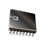
| 产品图片 |
|
| rohs | 符合RoHS无铅 / 符合限制有害物质指令(RoHS)规范要求 |
| 产品系列 | 接口 IC,数字隔离器,Analog Devices ADUM6132ARWZIsoPower®, iCoupler® |
| 数据手册 | |
| 产品型号 | ADUM6132ARWZ |
| PCN设计/规格 | |
| PulseWidthDistortion(Max) | 10ns |
| 上升/下降时间(典型值) | 15ns, 15ns |
| 产品目录页面 | |
| 产品种类 | |
| 传播延迟tpLH/tpHL(最大值) | 100ns, 100ns |
| 传播延迟时间 | 100 ns |
| 供应商器件封装 | 16-SOIC W |
| 共模瞬态抗扰度(最小值) | 50kV/µs |
| 其它图纸 |
|
| 功率耗散 | 275 mW |
| 包装 | 管件 |
| 商标 | Analog Devices |
| 安装类型 | 表面贴装 |
| 安装风格 | SMD/SMT |
| 封装 | Tube |
| 封装/外壳 | 16-SOIC(0.295",7.50mm 宽) |
| 封装/箱体 | SOIC-16 |
| 工作温度 | -40°C ~ 85°C |
| 工厂包装数量 | 47 |
| 技术 | 磁耦合 |
| 数据速率 | 1MHz |
| 最大工作温度 | + 85 C |
| 最小工作温度 | - 40 C |
| 标准包装 | 47 |
| 电压-正向(Vf)(典型值) | - |
| 电压-电源 | 4.5 V ~ 5.5 V, 12.5 V ~ 17 V |
| 电压-隔离 | 3750Vrms |
| 电流-DC正向(If) | - |
| 电流-峰值输出 | - |
| 电流-输出高,低 | - |
| 电源电压-最大 | 5.5 V |
| 电源电压-最小 | 4.5 V |
| 电源电流 | 350 mA |
| 类型 | General Purpose |
| 系列 | ADUM6132 |
| 绝缘电压 | 3.75 kVrms |
| 脉宽失真(最大) | 10ns |
| 视频文件 | http://www.digikey.cn/classic/video.aspx?PlayerID=1364138032001&width=640&height=505&videoID=2219593469001http://www.digikey.cn/classic/video.aspx?PlayerID=1364138032001&width=640&height=505&videoID=2474710092001 |
| 认可 | CSA, UR |
| 输入-输入侧1/输入侧2 | 2/0 |
| 通道数 | 1 |
| 通道数量 | 1 Channel |


- 商务部:美国ITC正式对集成电路等产品启动337调查
- 曝三星4nm工艺存在良率问题 高通将骁龙8 Gen1或转产台积电
- 太阳诱电将投资9.5亿元在常州建新厂生产MLCC 预计2023年完工
- 英特尔发布欧洲新工厂建设计划 深化IDM 2.0 战略
- 台积电先进制程称霸业界 有大客户加持明年业绩稳了
- 达到5530亿美元!SIA预计今年全球半导体销售额将创下新高
- 英特尔拟将自动驾驶子公司Mobileye上市 估值或超500亿美元
- 三星加码芯片和SET,合并消费电子和移动部门,撤换高东真等 CEO
- 三星电子宣布重大人事变动 还合并消费电子和移动部门
- 海关总署:前11个月进口集成电路产品价值2.52万亿元 增长14.8%


PDF Datasheet 数据手册内容提取
Isolated Half-Bridge Gate Driver with Integrated Isolated High-Side Supply Data Sheet ADuM6132 FEATURES GENERAL DESCRIPTION isoPower integrated isolated high-side supply The ADuM61321 is an isolated half-bridge gate driver that 275 mW isolated dc-to-dc converter employs the Analog Devices, Inc., iCoupler® technology to 200 mA output sink current, 200 mA output source current provide an isolated high-side driver with an integrated 275 mW High common-mode transient immunity: >50 kV/µs high-side supply. This supply, provided by an internal isolated Wide-body 16-lead SOIC package dc-to-dc converter, powers not only the ADuM6132 high-side Safety and regulatory approvals output but also any external buffer circuitry that is commonly UL recognition used with the ADuM6132. This functionality eliminates the 3750 V rms for 1 minute per UL 1577 cost, space, and performance issues associated with external CSA Component Acceptance Notice #5A supply configurations such as a bootstrap circuit. CSA/IEC 60950-1, 400 V rms The architecture of the ADuM6132 isolates the high-side VDE certificate of conformity (pending) channel and the high-side power from the control and low- DIN V VDE V 0884-10 (VDE V 0884-10):2006-12 side interface circuitry. Care has been taken to ensure close V = 560 V peak IORM matching between the high-side and low-side driver timing characteristics to reduce the need for a dead time margin. APPLICATIONS In comparison to gate drivers that employ high voltage level MOSFET/IGBT gate drivers translation methodologies, the ADuM6132 offers the benefit Motor drives of true, galvanic isolation. The differential voltage between Solar panel inverters high-side and low-side channels can be as high as 800 V with Power supplies good insulation lifetime (see Table 12). isoPower® uses high frequency switching elements to transfer power through its transformer. Special care must be taken during printed circuit board (PCB) layout to meet emissions standards. Refer to the AN-0971 Application Note for information about board layout considerations. FUNCTIONAL BLOCK DIAGRAM VDD 1 ISOLATED 16VISO DC-TO-DC GND 2 CONVERTER 15 GNDISO VDDL 3 14 GNDA DT VIA 4 ENCODE ANHIF 13 VDDA VVOIBB 56 LEVEL-SHIFT DECODE LEVEL-S 1121 VNOCA VDDB 7 10 NC GND 8 ADuM6132 9 GNDISO 07393-001 Figure 1. 1 Protected by U.S. Patents 5,952,849; 6,873,065; 6,903,578; 7,075,329; and other pending patents. Rev. B Document Feedback Information furnished by Analog Devices is believed to be accurate and reliable. However, no responsibility is assumed by Analog Devices for its use, nor for any infringements of patents or other One Technology Way, P.O. Box 9106, Norwood, MA 02062-9106, U.S.A. rights of third parties that may result from its use. Specifications subject to change without notice. No license is granted by implication or otherwise under any patent or patent rights of Analog Devices. Tel: 781.329.4700 ©2008–2014 Analog Devices, Inc. All rights reserved. Trademarks and registered trademarks are the property of their respective owners. Technical Support www.analog.com
ADuM6132 Data Sheet TABLE OF CONTENTS Features .............................................................................................. 1 ESD Caution...................................................................................6 Applications ....................................................................................... 1 Pin Configuration and Function Descriptions ..............................7 General Description ......................................................................... 1 Typical Performance Characteristics ..............................................8 Functional Block Diagram .............................................................. 1 Terminology .................................................................................... 10 Revision History ............................................................................... 2 Applications Information .............................................................. 11 Specifications ..................................................................................... 3 Typical Application Usage ......................................................... 11 Electrical Characteristics ............................................................. 3 PCB Layout ................................................................................. 11 Package Characteristics ............................................................... 4 Thermal Analysis ....................................................................... 12 Regulatory Information ............................................................... 4 Undervoltage Lockout ............................................................... 12 Insulation and Safety-Related Specifications ............................ 4 Propagation Delay-Related Parameters ................................... 13 DIN V VDE V 0884-10 (VDE V 0884-10) Insulation Magnetic Field Immunity .......................................................... 13 Characteristics .............................................................................. 5 Insulation Lifetime ..................................................................... 14 Recommended Operating Conditions ...................................... 5 Outline Dimensions ....................................................................... 15 Absolute Maximum Ratings ............................................................ 6 Ordering Guide .......................................................................... 15 REVISION HISTORY 4/14—Rev. A to Rev. B Change to Table 3 ............................................................................. 4 6/12—Rev. 0 to Rev. A Created Hyperlink for Safety and Regulatory Approvals Entry in Features Section ................................................................. 1 Changes to Regulatory Information Section and Table 3 ........... 4 Change to PCB Layout Section ..................................................... 12 Updated Outline Dimensions ....................................................... 15 7/08—Revision 0: Initial Version Rev. B | Page 2 of 16
Data Sheet ADuM6132 SPECIFICATIONS ELECTRICAL CHARACTERISTICS All voltages are relative to their respective ground; 4.5 V ≤ V = V ≤ 5.5 V; 12.5 V ≤ V ≤ 17.0 V; V = V . All minimum/maximum DD DDL DDB DDA ISO specifications apply over the entire recommended operating range, unless otherwise noted. All typical specifications are at T = 25°C, A V = V = 5.0 V, V = 15 V, V = V . DD DDL DDB DDA ISO Table 1. Parameter Symbol Min Typ Max Unit Test Conditions/Comments DC SPECIFICATIONS Isolated Power Supply Input Current, Quiescent I 280 mA I = 0 mA, dc signal inputs DD(Q) ISO Input Current, Loaded I 350 mA I = I DD ISO ISO(MAX) Maximum Output Current1 I 22 mA 12.5 V ≤ V ≤ 17.0 V ISO(MAX) ISO Output Voltage V 12.5 15 17 V 0 mA ≤ I ≤ 22 mA ISO ISO Logic Supply Input Current I 1.8 3.0 mA DDL Output Supplies, Channel A or Channel B2 Supply Current, Quiescent I , I 1.0 2.0 mA DDA(Q) DDB(Q) Supply Current, f = 20 kHz I , I 1.1 2.1 mA C = 200 pF IN DDA(20) DDB(20) L Supply Current, f = 100 kHz I , I 1.3 2.3 mA C = 200 pF IN DDA(100) DDB(100) L Supply Current, f = 1000 kHz I , I 4.5 5.5 mA C = 200 pF IN DDA(1000) DDB(1000) L Logic Inputs, Channel A or Channel B Input Current I , I −10 +0.01 +10 µA 0 V ≤ V , V ≤ 5.5 V IA IB IA IB Logic High Input Voltage V , V 0.7 × V V IAH IBH DDL Logic Low Input Voltage V , V 0.3 × V V IAL IBL DDL Outputs, Channel A or Channel B Channel A High Level Output Voltage V V − 0.1 V I = −1 mA OAH DDA OAH Channel B High Level Output Voltage V V − 0.1 V I = −1 mA OBH DDB OBH Low Level Output Voltages V ,V 0.1 V I , I = 1 mA OAL OBL OAL OBL High Level Output Current, Peak3 I , I 200 mA OAH OBH Low Level Output Current, Peak3 I , I 200 mA OAL OBL Undervoltage Lockout, V or V Supply4 DDA DDB Positive Going Threshold V , V 11.0 11.7 12.3 V DDAUV+ DDBUV+ Negative Going Threshold V , V 10.0 10.7 11.2 V DDAUV− DDBUV− Hysteresis V , V 1.0 V DDAUVH DDBUVH Undervoltage Lockout, V Supply4 DDL Positive Going Threshold V 3.5 4.2 V DDLUV+ Negative Going Threshold V 3.1 3.8 V DDLUV− Hysteresis V 0.5 V DDLUVH SWITCHING SPECIFICATIONS Minimum Pulse Width1 PW 50 ns C = 200 pF L Maximum Switching Frequency1 f 1000 kHz C = 200 pF IN L Propagation Delay1 t , t 40 60 100 ns C = 200 pF PHL PLH L Change vs. Temperature 100 ps/°C Pulse Width Distortion, |t − t | PWD 10 ns C = 200 pF PLH PHL L Channel-to-Channel Matching, Rising or t 20 ns C = 200 pF M2 L Falling Matching Edge Polarity1 Channel-to-Channel Matching, Rising vs. t 20 ns C = 200 pF M1 L Falling Opposite Edge Polarity1 Rev. B | Page 3 of 16
ADuM6132 Data Sheet Parameter Symbol Min Typ Max Unit Test Conditions/Comments Part-to-Part Matching1 60 ns C = 200 pF L Output Rise Time (10% to 90%) t 15 ns C = 200 pF R L Output Fall Time (10% to 90%) t 15 ns C = 200 pF F L 1 See the Terminology section. 2 IDDA is supplied by the output of the integrated isolated dc-to-dc power supply. IDDB is supplied by an external power connection to the VDDB pin. See Figure 16. 3 Duration less than 1 second. Average output current must conform to the limit shown in the Absolute Maximum Ratings section. 4 Undervoltage lockout (UVLO) holds the outputs in a low state if the corresponding input or output power supply is below the referenced threshold. Hysteresis is built into the detection threshold to prevent oscillations and noise sensitivity. PACKAGE CHARACTERISTICS Table 2. Parameter Symbol Min Typ Max Unit Test Conditions/Comments Resistance (Input Side to High-Side Output)1 R 1012 Ω I-O Capacitance (Input Side to High-Side Output)1 C 2.0 pF I-O Input Capacitance C 4.0 pF I Junction-to-Ambient Thermal Resistance θ 45 °C/W 4-layer PCB JA 1 The device is considered a two-terminal device: Pin 1 through Pin 8 are shorted together, and Pin 9 through Pin 16 are shorted together. REGULATORY INFORMATION Table 3. UL CSA VDE (Pending) Recognized under UL 1577 Approved under CSA Component Acceptance Certified according to DIN V VDE V 0884-10 component recognition program1 Notice #5A (VDE V 0884-10):2006-122 Single protection, Basic insulation per CSA 60950-1-03 and IEC 60950-1, Reinforced insulation, 560 V peak 3750 V rms isolation voltage 400 V rms (566 V peak) maximum working voltage Reinforced insulation per CSA 60950-1-03 and IEC 60950-1, 250 V rms (354 V peak) maximum working voltage File E214100 File 205078 File 2471900-4880-0001 1 In accordance with UL 1577, each ADuM6132 is proof-tested by applying an insulation test voltage ≥ 4500 V rms for 1 second (current leakage detection limit = 10 µA). 2 In accordance with DIN V VDE V 0884-10, each ADuM6132 is proof-tested by applying an insulation test voltage ≥ 1050 V peak for 1 second (partial discharge detection limit = 5 pC). The asterisk (*) marking branded on the component designates DIN V VDE V 0884-10 approval. INSULATION AND SAFETY-RELATED SPECIFICATIONS Table 4. Parameter Symbol Value Unit Test Conditions/Comments Rated Dielectric Insulation Voltage 3750 V rms 1 minute duration Minimum External Air Gap (Clearance) L(I01) >8.0 mm Measured from input terminals to output terminals, shortest distance through air Minimum External Tracking (Creepage) L(I02) >8.0 mm Measured from input terminals to output terminals, shortest distance path along body Minimum Internal Gap (Internal Clearance) 0.017 min mm Insulation distance through insulation Tracking Resistance (Comparative Tracking Index) CTI >175 V DIN IEC 112/VDE 0303 Part 1 Isolation Group IIIa Material Group (DIN VDE 0110, 1/89, Table 1) Rev. B | Page 4 of 16
Data Sheet ADuM6132 DIN V VDE V 0884-10 (VDE V 0884-10) INSULATION CHARACTERISTICS The ADuM6132 is suitable for reinforced electrical isolation only within the safety limit data. Maintenance of the safety data is ensured by protective circuits. The asterisk (*) marking on the package denotes DIN V VDE V 0884-10 approval. Table 5. Parameter Test Conditions/Comments Symbol Value Unit Installation Classification per DIN VDE 0110 For Rated Mains Voltage ≤ 150 V rms I to IV For Rated Mains Voltage ≤ 300 V rms I to III For Rated Mains Voltage ≤ 400 V rms I to II Climatic Classification 40/105/21 Pollution Degree (DIN VDE 0110, Table 1) 2 Maximum Working Insulation Voltage V 560 V peak IORM Input-to-Output Test Voltage, Method B1 V × 1.875 = V , 100% production test, t = 1 sec, V 1050 V peak IORM PR m PR partial discharge <5 pC Input-to-Output Test Voltage, Method A V PR After Environmental Tests Subgroup 1 V × 1.6 = V , t = 60 sec, partial discharge <5 pC 896 V peak IORM PR m After Input and/or Safety Test Subgroup 2 V × 1.2 = V , t = 60 sec, partial discharge <5 pC 672 V peak IORM PR m and Subgroup 3 Highest Allowable Overvoltage Transient overvoltage, t = 10 sec V 6000 V peak TR TR Safety-Limiting Values Maximum value allowed in the event of a failure (see Figure 2) Case Temperature T 150 °C S Side 1 Current I 555 mA S1 Insulation Resistance at T V = 500 V R >109 Ω S IO S 600 RECOMMENDED OPERATING CONDITIONS A) m 500 Table 6. NT ( Parameter Rating E URR 400 Operating Temperature Range, TA −40°C to +85°C CD Input Supply Voltage, VDD and VDDL1 4.5 V to 5.5 V D G V 300 Channel A, Channel B Supply Voltage, 12.5 V to 17 V TIN VDDA and VDDB1 A R 200 Input Signal Rise and Fall Times 1 ms E P O Common-Mode Transient Immunity, −50 kV/µs to +50 kV/µs E AF 100 Input to Output S Minimum Power-On Slew Rate (P ), 1 V/ms SLEW V and V 2 0 DD DDL 0 50AMBIENT TEM1P00ERATURE (°C1)50 200 07393-002 1 All voltages are relative to their respective ground. Figure 2. Thermal Derating Curve, Dependence of Safety-Limiting Values 2 The ADuM6132 power supply may fail to properly initialize if VDD and VDDL are applied too slowly. The power supply slew rate must be faster than specified with Ambient Temperature per DIN V VDE V 0884-10 over the entire turn-on ramp. Power-on should start from a completely discharged state. Rev. B | Page 5 of 16
ADuM6132 Data Sheet ABSOLUTE MAXIMUM RATINGS T = 25°C, unless otherwise noted. Stresses above those listed under Absolute Maximum Ratings A may cause permanent damage to the device. This is a stress Table 7. rating only; functional operation of the device at these or any Parameter Rating other conditions above those indicated in the operational Storage Temperature Range, T −55°C to +150°C ST section of this specification is not implied. Exposure to absolute Ambient Operating Temperature −40°C to +85°C maximum rating conditions for extended periods may affect Range, T A device reliability. Input Supply Voltage, V , V 1 −0.5 V to +7.0 V DDL DD Channel A, Channel B Supply −0.5 V to +27 V Voltage, VDDA, VDDB1 ESD CAUTION Input Voltage, V , V 1 −0.5 V to V + 0.5 V IA IB DDL Output Voltage, V 1 −0.5 V to V + 0.5 V OA ISO Output Voltage, V 1 −0.5 V to V + 0.5 V OB DDB Average DC Output Current, −10 mA to +10 mA I , I OA OB Peak Output Current, IOA, IOB −200 mA to +200 mA Common-Mode Transients2 −100 kV/µs to +100 kV/µs 1 All voltages are relative to their respective ground. 2 Refers to common-mode transients across any insulation barrier. Common- mode transients exceeding the absolute maximum ratings can cause latch-up or permanent damage. Rev. B | Page 6 of 16
Data Sheet ADuM6132 PIN CONFIGURATION AND FUNCTION DESCRIPTIONS VDD 1 16 VISO GND 2 15 GNDISO VDDL 3 ADuM6132 14 GNDA VIA 4 TOP VIEW 13 VDDA VIB 5 (Not to Scale) 12 VOA VOB 6 11 NC VDDB 7 10 NC GND 8NC = NO CONNECT9 GNDISO 07393-003 Figure 3. Pin Configuration Table 8. Pin Function Descriptions Pin No. Mnemonic Description 1 V Input Supply Voltage for Isolated Power Supply, 4.5 V to 5.5 V. DD 2, 8 GND Ground Reference for Isolated Power Supply Input and Logic Inputs. 3 V Input Supply Voltage for Logic, 4.5 V to 5.5 V. DDL 4 V Logic Input A. IA 5 V Logic Input B. IB 6 V Output B (Nonisolated). OB 7 V Output B Supply Voltage Input (Nonisolated), 12.5 V to 17 V. DDB 9, 15 GND Ground Reference for Isolated Power Supply Output. ISO 10, 11 NC No Connect. 12 V Output A (Isolated). OA 13 V Output A Supply Voltage Input. Must be connected externally to V (Pin 16). DDA ISO 14 GND Output A Ground Reference. Must be connected externally to GND (Pin 15). A ISO 16 V Isolated Power Supply Voltage Output. ISO Table 9. Truth Table (Positive Logic)1 V Input V Input V State V State V Output V Output Notes IA IB DDL DDB OA OB L L Powered Powered L L L H Powered Powered L H H L Powered Powered H L H H Powered Powered H H X X Unpowered Powered L L V returns to input state within 1 μs of V OA DDL power restoration X X Powered Unpowered L L 1 L = low; H = high; X = high or low. Rev. B | Page 7 of 16
ADuM6132 Data Sheet TYPICAL PERFORMANCE CHARACTERISTICS All typical performance curves are based on operation at T = 25°C, unless otherwise noted. A 16.0 1.2 15.5 1.0 VDD = 5.0V W) 15.0 TION ( 0.8 VDD = 4.5V VDD = 5.5V (V)O14.5 VDD = 5.5V SIPA 0.6 S S VI DI VDD = 4.5V ER 14.0 W 0.4 O VDD = 5.0V P 13.5 0.2 13.00 5 IISO LO10AD CURREN15T (mA) 20 25 07393-024 00 5 IISOLO10AD CURREN15T (mA) 20 25 07393-027 Figure 4. Typical VISO Supply Voltage vs. IISO External Load Figure 7. Typical Total Power Dissipation vs. IISO External Load 300 14.8 VDD = 4.5V 14.6 VDD = 5.5V 250 VDD = 5.0V 14.4 RRENT (mA) 200 VDD = 5.5V A LOAD (V) 111344...802 VDD = 5.0V U 150 m UT C T 22 13.6 INPDD100 V AISO 1133..24 VDD = 4.5V I 50 13.0 12.8 00 5 IISO LO10AD CURREN15T (mA) 20 25 07393-025 12.6–40 –20 0AMBIE2N0T TEM4P0ERATU6R0E (°C)80 100 120 07393-028 Figure 5. Typical IDD Supply Current vs. IISO External Load Figure 8. Typical VISO Output Voltage at Maximum Combined Load over Temperature 30 2500 VDD = 5.5V 25 2000 VDD = 4.5V W) VDD = 4.5V m CIENCY (%) 1250 VDD = 5.0V SSIPATION (1500 VDD = 5.0V FI DI1000 EF 10 WER VDD = 5.5V O P 500 5 00 5 IISO LO10AD CURREN15T (mA) 20 25 07393-026 01 VIS1O0 LOAD IMPEDANCE10 (0Ω) 100007393-029 Figure 6. Typical VISO Supply Efficiency vs. IISO External Load Figure 9. Power Dissipation vs. Load Impedance for Fault Conditions Rev. B | Page 8 of 16
Data Sheet ADuM6132 6 4 5 VDDA = 17V V) 3 mA) 4 AGE ( NT ( OLT CURREA 3 VDDA = 12.5V UTPUT V 2 IDD 2 VDDA = 15V OL VO 1 1 00 200 VOA DA4T0A0 FREQUE6N0C0Y (kHz) 800 100007393-030 00 50 100IOL (mA)150 200 250 07393-033 Figure 10. Typical IDDA Supply Current, CL = 200 pF Figure 13. Typical VOL vs. IOL (VDD = VDDL = 5 V, VDDA = VDDB = 12 V to 17 V) 6 70 5 s) NT (mA) 4 VDDB = 17V N DELAY (n 65 tPLH CHA E O RR 3 ATI 60 U G C A I DDB 2 VDDB = 12.5V PROP tPHL CHA VDDB = 15V OA 55 V 1 00 200 VOB DA4T0A0 FREQUE6N0C0Y (kHz) 800 100007393-031 50–50 –25 0TEMPE2R5ATURE (5°0C) 75 100 07393-034 Figure 11. Typical IDDB Supply Current, CL = 200 pF Figure 14. Typical Channel A Propagation Delay vs. Temperature 0 70 V) P ( O –1 s) AGE DR ELAY (n 65 tPLH CHB OLT –2 N D V O UT ATI 60 tPHL CHB P G T –3 A U P O O – V) HDD –4 V PROB 55 O V ( –50 50 100IOH (mA)150 200 250 07393-032 50–50 –25 0TEMPE2R5ATURE (5°C0) 75 100 07393-035 Figure 12. Typical VOH Voltage Drop vs. IOH (VDD = VDDL = 5 V, Figure 15. Typical Channel B Propagation Delay vs. Temperature VDDA = VDDB = 12 V to 17 V) Rev. B | Page 9 of 16
ADuM6132 Data Sheet TERMINOLOGY Channel-to-Channel Matching Minimum Pulse Width Channel-to-channel matching with rising or falling matching The minimum pulse width is the shortest pulse width at which edge polarity is the magnitude of the propagation delay differ- the specified pulse width distortion is guaranteed. Operation ence between two channels of the same part when the inputs below the minimum pulse width is not recommended. are both rising edges or both falling edges. The loads on each Part-to-Part Matching channel are equal. Part-to-part matching is the magnitude of the propagation Channel-to-channel matching with rising vs. falling opposite delay difference between the same channels of two different edge polarity is the magnitude of the propagation delay differ- parts. This includes rising vs. rising edges, falling vs. falling ence between two channels of the same part when one input is edges, or rising vs. falling edges. The supply voltages, temp- a rising edge and one input is a falling edge. The loads on each eratures, and loads of each part are equal. channel are equal. Propagation Delay Maximum Output Current The propagation delay is the time that it takes a logic signal to The maximum output current is the maximum isolated supply propagate through a component. The propagation delay to a current that the ADuM6132 can provide. This current supports logic low output may differ from the propagation delay to a external loads as well as the needs of the ADuM6132 Channel A logic high output. output circuitry. This is achieved via external connection of the The t propagation delay is measured from the 50% level PHL V pin to the V pin and of the GND pin to the GND pin ISO DDA ISO A of the falling edge of the V or V signal to the 50% level of IA IB (see Figure 16). The net current available to power external loads the falling edge of the V or V signal. The t propagation OA OB PLH is the ADuM6132 output current, I , minus the Channel A ISO delay is measured from the 50% level of the rising edge of the supply current, I . DDA V or V signal to the 50% level of the rising edge of the V IA IB OA Maximum Switching Frequency or VOB signal. The maximum switching frequency is the maximum signal Capacitive Load (C ) L frequency at which the specified timing parameters are guar- The output capacitive load simulates a typical FET, IGBT, or anteed. Operation beyond the maximum switching frequency buffer for timing or current measurements. This load includes is not recommended, because high switching rates can cause all discrete and parasitic capacitive loads on the output. droop in the output supply voltage. Rev. B | Page 10 of 16
Data Sheet ADuM6132 APPLICATIONS INFORMATION TYPICAL APPLICATION USAGE greatest amount of design flexibility. The precise buffer/high voltage transistor combination can be selected to suit the The architecture of the ADuM6132 is ideal for motor drive and requirements of the application. inverter applications where the low-side channels are common to the controller. This arrangement requires only two isolation PCB LAYOUT regions in a package. All the isolated signals and the isolated The ADuM6132 digital isolator with integrated 275 mW power are grouped on one side of the package to maintain full isoPower dc-to-dc converter requires no external interface package creepage and clearance. The low-side driver, as well as the circuitry for the logic interfaces. Power supply bypassing is control signals, share a common reference and are also grouped. required at the input and output supply pins (see Figure 17). To maximize the effectiveness of external bypass capacitors, the The power supply section of the ADuM6132 uses a very high isoPower dc-to-dc converter is not internally tied to the data oscillator frequency to efficiently pass power through its chip channels, and should be treated as a completely independent scale transformers. In addition, the normal operation of the subsystem, except for a UVLO function (see the Undervoltage data section of the iCoupler introduces switching transients Lockout section). This means that power must be applied to VDD on the power supply pins. Bypass capacitors are required for to operate the dc-to-dc converter. Power must also be applied to several operating frequencies. Noise suppression requires a low VDDL and VDDB to operate the data input and the Channel B ESR, high frequency capacitor; ripple suppression and proper driver output. On the secondary side, the power generated at regulation require a large value capacitor in parallel (see Table 10). the VISO pin must be applied as an input power supply to the The total lead length between both ends of the capacitor and VDDA pin. GNDISO and GNDA must also be connected. the input power supply pin should not exceed 20 mm. The ADuM6132 is intended for use in driving low gate Table 10. Recommended Bypass Capacitors capacitance transistors (200 pF typically). Most high voltage Supply Pins Bypass Capacitors applications involve larger transistors than this. To accom- V 1, 2 0.1 μF, 10 μF DD modate these applications, users can implement a buffer V 7, 8 0.1 μF DDB configuration with the ADuM6132, as shown in Figure 16. In V 2, 3 0.1 μF many cases, this buffer configuration is the least expensive DDL V 13, 14 0.1 μF option to drive high capacitance devices and provides the DDA V 15, 16 0.1 μF, 10 μF ISO ADuM6132 VDC+ VDD VISO +5V 1 ISOLATED 16 10µF 0.1µF DC-TO-DC 0.1µF GND GND 2 CONVERTER 15 GNDISO IISO 0.1µF 9 GNDISO VDDL VDDA IDDA IAVAIL +5V 3 13 BUFFER 0.1µF VIA ISOLATED VOA CBUF RG 4 GATE 12 DRIVE RBUF GNDA 14 VDDB +15V +15V 7 0.1µF CBUF BUFFER VIB 5 NONDIGSRAOITVLEEATED 6 VOB RBUF RG GND 8 GND VDC– 07393-016 Figure 16. Typical Application Circuit Rev. B | Page 11 of 16
ADuM6132 Data Sheet In applications involving high common-mode transients, care UNDERVOLTAGE LOCKOUT should be taken to ensure that board capacitive coupling across The ADuM6132 has undervoltage lockout (UVLO) circuits on the isolation barrier is minimized. Furthermore, the board the V , V , and V supplies. For each supply, the respective DDL DDA DDB layout should be designed so that any coupling that does occur UVLO circuit monitors the supply voltage and takes a predeter- affects all pins on a given component side equally. Failure to mined action based on whether the supply voltage is above or ensure this may cause voltage differentials between pins that below a given threshold. These thresholds are specified in Table 1. exceed the absolute maximum ratings of the device (see Table 7), In the recommended configuration shown in Figure 16, only leading to latch-up or permanent damage. two independent supplies are controlled by the user: V and DDB VDD VISO GND GNDISO VDDL/VDD (VDDL = VDD in Figure 16). VDDA is supplied by the VDDL GNDA internal dc-to-dc converter via the VISO = VDDA external connec- VIA VDDA VIB VOA tion. Nevertheless, the VDDA UVLO functionality is included in VGVDNODDBB NNGCCNDISO 07393-017 Tdac-btloe- 1d1c tcoo nshvoerwte hro pwo wtheer sV oOnA aonudtp ouftf .b ehaves when the internal Figure 17. Recommended PCB Layout Table 11. Undervoltage Lockout Functionality1 The ADuM6132 is a power device that dissipates approximately User-Provided VISO Powered Supplies Supply 1 W of power when fully loaded and running at maximum speed. V V V Effect Because it is not possible to apply a heat sink to an isolation DDL DDB DDA H H H Normal operation. device, the device depends primarily on heat dissipation into Internal dc-to-dc converter is the PCB through the GND pins. If the device will be used at active. high ambient temperatures, provide a thermal path from the V /V output logic states OA OB GND pins to the PCB ground plane. match VIA/VIB input logic states. H H L Internal dc-to-dc converter is The board layout in Figure 17 shows enlarged pads for Pin 8 active but V is below UVLO ISO (GND) and Pin 9 (GNDISO). Multiple vias should be implemented threshold. from the pad to the ground plane. This layout significantly reduces VOA output is driven low. V output operates normally. the temperatures inside the chip. The dimensions of the expanded OB X L X Internal dc-to-dc converter is pads are left to the discretion of the designer and the available turned off (V = 0 V). ISO board space. See the AN-0971 Application Note for board V output is driven low. OA layout recommendations. VOB output is driven low. L X X Internal dc-to-dc converter is THERMAL ANALYSIS turned off (V = 0 V). ISO The ADuM6132 consists of several internal die attached to VOA output is driven low. V output is driven low. two lead frame paddles. For the purposes of thermal analysis, OB the part is treated as a thermal unit with the highest junction 1 H: supply voltage > UVLO threshold; L: supply voltage < UVLO threshold; temperature determining θ , as shown in Table 2. The value of X: supply voltage level is irrelevant. JA θJA is based on measurements taken with the part mounted on When all three supplies are above their respective UVLO a JEDEC standard 4-layer board with fine width traces and still thresholds, the ADuM6132 operates normally. The internal air. Under normal operating conditions, the ADuM6132 oper- dc-to-dc converter is active, and both outputs operate as ates at full load across the full temperature range without derating determined by their respective input logic signals. If either of the output current. However, following the recommendations in the user-provided supplies is below its UVLO threshold, the the PCB Layout section decreases the thermal resistance to the ADuM6132 is put into a disabled mode. In this mode, the PCB, allowing increased thermal margin at high ambient internal dc-to-dc converter is turned off and both outputs are temperatures. driven low. Under VISO output short-circuit conditions, as shown in The VOB output is driven low by either the VDDL or VDDB Figure 9, the package power dissipation quickly exceeds the safe UVLO circuit (whichever is below its threshold). The V OA operating limit of 1.44 W for ambient temperatures up to 85°C. output is driven low when the internal dc-to-dc converter is At low input voltage, the power dissipation can approach 2 W. turned off. The V supply voltage drops to 0 V, causing V ISO DDA Because internal compensation of the PWM makes low VDD a to drop also because VISO and VDDA are externally connected. worst-case condition, input voltage limiting is not an effective When V is below its UVLO threshold, the V UVLO DDA DDA strategy for protecting the ADuM6132 from output load fault circuit drives V low. OA conditions. Therefore, the preferred protection methods, where required, are either limiting ambient temperature to 60°C or the use of a fuse. Rev. B | Page 12 of 16
Data Sheet ADuM6132 PROPAGATION DELAY-RELATED PARAMETERS 100 X U Propagation delay is a parameter that describes the time it takes L F a logic signal to propagate through a component. The propaga- TIC 10 E tion delay to a logic low output may differ from the propagation N delay to a logic high output. E MAGgauss) 1 Lk INPUT (VIx) tPLH tPHL 50% ALLOWABDENSITY (0.1 OUTPUT (VOx) 50% 07393-018 XIMUM 0.01 A Figure 18. Propagation Delay Parameters M Pthuelssee twwiod tphr odpisatgoarttiioonn dise tlhaye vmaaluxeims aunmd idsi fafner ienndciec abteiotwn eoefn h ow 0.0011k 10kMAGNETI1C0 0FkIELD FREQ1MUENCY (Hz1)0M 100M 07393-019 accurately the timing of the input signal is preserved. Figure 19. Maximum Allowable External Magnetic Flux Density Channel-to-channel matching refers to the maximum amount For example, at a magnetic field frequency of 1 MHz, the that the propagation delay differs between channels within a maximum allowable magnetic flux density of 0.2 kgauss single ADuM6132 component. induces a voltage of 0.25 V at the receiving coil. This voltage MAGNETIC FIELD IMMUNITY is approximately 50% of the sensing threshold and does not cause a faulty output transition. Similarly, if such an event The ADuM6132 is extremely immune to external magnetic occurs during a transmitted pulse (with the worst-case polarity), fields. The limitation on the ADuM6132 magnetic field immunity the received pulse is reduced from >1.0 V to 0.75 V—still well is set by the condition in which induced voltage in the receiving above the 0.5 V sensing threshold of the decoder. coil of the transformer is sufficiently large to falsely set or reset the decoder. The following analysis defines the conditions The preceding magnetic flux density values correspond to under which this may occur. specific current magnitudes at given distances from the ADuM6132 transformers. Figure 20 expresses these allowable The pulses at the transformer output have an amplitude greater current magnitudes as a function of frequency for selected than 1.0 V. The decoder has a sensing threshold at approximately distances. As shown in Figure 20, the ADuM6132 is extremely 0.5 V, thus establishing a 0.5 V margin in which induced voltages immune and can be affected only by extremely large currents can be tolerated. The voltage induced across the receiving coil is operated at high frequency and very close to the component. given by For example, at a magnetic field frequency of 1 MHz, a 0.5 kA V = (−dβ/dt) Σπrn2 ; n = 1, 2, … N current would need to be placed 5 mm away from the ADuM6132 where: to affect the operation of the component. 1000 β is the magnetic flux density (gauss). rn is the radius of the nth turn in the receiving coil (cm). kA) DISTANCE = 1m N is the number of turns in the receiving coil. T ( 100 N E R Given the geometry of the receiving coil in the ADuM6132 and R U C an imposed requirement that the induced voltage be at most E 10 L 50% of the 0.5 V margin at the decoder, a maximum allowable AB DISTANCE = 100mm W magnetic flux density is calculated, as shown in Figure 19. O L 1 L A DISTANCE = 5mm M U M XI 0.1 A M 0.01 1k 10MkAGNET1IC0 0FkIELD FRE1QMUENCY (H1z0)M 100M 07393-020 Figure 20. Maximum Allowable Current for Various Current-to-ADuM6132 Spacings Rev. B | Page 13 of 16
ADuM6132 Data Sheet Note that in the presence of strong magnetic fields and high In the case of unipolar ac or dc voltage, the stress on the frequencies, any loops formed by PCB traces may induce insulation is significantly lower, which allows operation at sufficiently large error voltages to trigger the threshold of higher working voltages while still achieving a 50-year service succeeding circuitry. Care should be taken in the layout of such life. The working voltages listed in Table 12 can be applied while traces to avoid this possibility. maintaining the 50-year minimum lifetime, provided that the voltage conforms to either the unipolar ac or dc voltage cases. INSULATION LIFETIME Any cross-insulation voltage waveform that does not conform to All insulation structures eventually break down when subjected Figure 22 or Figure 23 should be treated as a bipolar ac waveform, to voltage stress over a sufficiently long period. The rate of insu- and its peak voltage should be limited to the 50-year lifetime lation degradation depends on the characteristics of the voltage voltage value listed in Table 12. Note that the voltage shown in waveform applied across the insulation. In addition to the testing Figure 22 is sinusoidal for illustration purposes only. It is meant performed by the regulatory agencies, Analog Devices conducts to represent any voltage waveform varying between 0 V and an extensive set of evaluations to determine the lifetime of the some limiting value. The limiting value can be positive or insulation structure within the ADuM6132. negative, but the voltage cannot cross 0 V. Analog Devices performs accelerated life testing using voltage levels higher than the rated continuous working voltage. Accel- eration factors for several operating conditions are determined. RATED PEAK VOLTAGE Twhoerskein fagc vtoorltsa aglelo. wTa cballec u12la tsiuomn mofa trhiez etsim thee t ore fcaoilmurme eant dtheed a pcetuaakl 0V 07393-021 working voltages for 50 years and 15 years of service life for Figure 21. Bipolar AC Waveform various operating conditions evaluated by Analog Devices. In many cases, the approved working voltage is higher than the RATED PEAK VOLTAGE 50-year service life voltage. Operation at these high working vTohleta ignessu claatnio lnea ldif etoti msheo ortfe tnheed A inDsuuMlat6io13n2 l idfee pine nsdosm oen c tahsees . 0V 07393-022 Figure 22. Unipolar AC Waveform voltage waveform type imposed across the isolation barrier. The iCoupler insulation structure degrades at different rates depending on whether the waveform is bipolar ac, unipolar ac, RATED PEAK VOLTAGE or dc. Figure 21, Figure 22, and Figure 23 illustrate these different isolation voltage waveforms. 0V 07393-023 Bipolar ac voltage is the most stringent environment. The goal Figure 23. DC Waveform of a 50-year operating lifetime under the bipolar ac condition determines the maximum working voltage recommended by Analog Devices. Table 12. Maximum Continuous Working Voltage1 Parameter Peak Voltage Lifetime AC Voltage, Bipolar Waveform 424 V peak 50-year minimum lifetime AC Voltage, Unipolar Waveform Basic Insulation 800 V peak 15-year minimum lifetime Basic Insulation 660 V peak 50-year minimum lifetime DC Voltage Waveform Basic Insulation 800 V peak 15-year minimum lifetime Basic Insulation 660 V peak 50-year minimum lifetime 1 Refers to continuous voltage magnitude imposed across the isolation barrier. See the Insulation Lifetime section for more information. Rev. B | Page 14 of 16
Data Sheet ADuM6132 OUTLINE DIMENSIONS 10.50(0.4134) 10.10(0.3976) 16 9 7.60(0.2992) 7.40(0.2913) 1 8 10.65(0.4193) 10.00(0.3937) 1.27(0.0500) 0.75(0.0295) BSC 2.65(0.1043) 0.25(0.0098) 45° 0.30(0.0118) 2.35(0.0925) 8° 0.10(0.0039) 0° COPLANARITY 0.10 0.51(0.0201) SPELAATNIENG 0.33(0.0130) 1.27(0.0500) 0.31(0.0122) 0.20(0.0079) 0.40(0.0157) C(RINOEFNPEATRRREOENNLCLTEIHNCEOGOSNDMELISPYM)LAEAIANNRNDSETIAORTRNOOESUJNANEORDDETEEDAICN-POSMPFTRIFALONLMPIDMIRLAELIRATIMTDEEESRTFSMEO;SRIRN-0ECU1QH3SU-EADIVAIINMAELDENENSSTIIOGSNNFS.OR 03-27-2007-B Figure 24. 16-Lead Standard Small Outline Package [SOIC_W] Wide Body (RW-16) Dimensions shown in millimeters and (inches) ORDERING GUIDE No. of Output Peak Output Package Model1 Channels Current (A) Voltage (V) Temperature Range Package Description Option ADuM6132ARWZ 2 0.2 15 −40°C to +85°C 16-Lead SOIC_W RW-16 ADuM6132ARWZ-RL 2 0.2 15 −40°C to +85°C 16-Lead SOIC_W, 13-inch Tape RW-16 and Reel Option (1,000 Units) 1 Z = RoHS Compliant Part. Rev. B | Page 15 of 16
ADuM6132 Data Sheet NOTES ©2008–2014 Analog Devices, Inc. All rights reserved. Trademarks and registered trademarks are the property of their respective owners. D07393-0-4/14(B) Rev. B | Page 16 of 16
Mouser Electronics Authorized Distributor Click to View Pricing, Inventory, Delivery & Lifecycle Information: A nalog Devices Inc.: ADUM6132ARWZ-RL ADUM6132ARWZ