 Datasheet下载
- 型号: ADUM5400ARWZ
- 制造商: Analog
- 库位|库存: xxxx|xxxx
- 要求:
| 数量阶梯 | 香港交货 | 国内含税 |
| +xxxx | $xxxx | ¥xxxx |
查看当月历史价格
查看今年历史价格
ADUM5400ARWZ产品简介:
ICGOO电子元器件商城为您提供ADUM5400ARWZ由Analog设计生产,在icgoo商城现货销售,并且可以通过原厂、代理商等渠道进行代购。 ADUM5400ARWZ价格参考¥50.39-¥50.39。AnalogADUM5400ARWZ封装/规格:数字隔离器, 通用 数字隔离器 2500Vrms 4 通道 1Mbps 25kV/µs CMTI 16-SOIC(0.295",7.50mm 宽)。您可以下载ADUM5400ARWZ参考资料、Datasheet数据手册功能说明书,资料中有ADUM5400ARWZ 详细功能的应用电路图电压和使用方法及教程。
ADUM5400ARWZ 是由 Analog Devices Inc.(现为 ADI 公司)生产的一款数字隔离器,属于 iCoupler 系列。该型号具有四通道双向隔离功能,支持最高 25 Mbps 的数据传输速率,适用于需要电气隔离的高速数字信号传输场景。以下是其主要应用场景:

1. 工业自动化与控制
   - 在工业控制系统中,ADUM5400ARWZ 可用于隔离现场设备(如传感器、执行器)和控制器之间的通信信号,防止噪声干扰和地环路问题,确保系统稳定运行。
   - 适用于 PLC(可编程逻辑控制器)、DCS(分布式控制系统)以及远程 I/O 模块。

2. 电机驱动与逆变器
   - 在电机驱动和逆变器应用中,该器件可用于隔离栅极驱动信号或反馈信号,保护控制电路免受高压影响。
   - 提供可靠的隔离屏障,同时支持快速信号传递。

3. 医疗设备
   - 医疗设备(如监护仪、超声设备、心电图机等)通常需要高精度的数据采集和隔离保护。ADUM5400ARWZ 可用于隔离患者接口电路与主控电路,保障患者和操作人员的安全。

4. 通信系统
   - 在通信接口设计中(如 RS-485、RS-232 或 CAN 总线),ADUM5400ARWZ 可提供信号隔离,避免长距离传输中的电磁干扰和电压浪涌对系统的影响。
   - 特别适合多节点网络环境下的数据通信。

5. 汽车电子
   - 在汽车电子领域,该器件可用于车载网络(如 LIN、CAN 总线)中的信号隔离,保护敏感电子单元免受瞬态电压冲击。
   - 支持电动汽车(EV)和混合动力汽车(HEV)中的高压电池管理系统(BMS)信号隔离。

6. 电源管理与转换
   - 在开关电源(SMPS)、DC-DC 转换器和光伏逆变器中,ADUM5400ARWZ 可用于隔离反馈信号或控制信号,确保系统的可靠性和安全性。

7. 消费类电子产品
   - 部分高端家用电器(如智能家电、家用能源管理系统)可能需要信号隔离功能,以提高产品的抗干扰能力和安全性。

总结:ADUM5400ARWZ 凭借其高性能的数字隔离能力,在工业、医疗、通信、汽车和消费电子等领域均有广泛的应用价值。其紧凑的封装形式(SOIC_Wide)和低功耗特性使其成为许多现代电子系统中理想的隔离解决方案。
| 参数 | 数值 |
| 产品目录 | |
| ChannelType | 单向 |
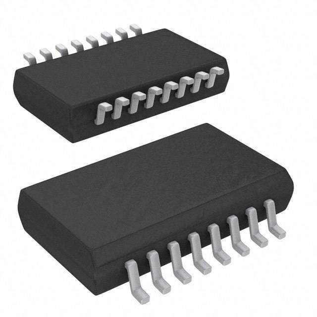
| 描述 | IC DGTL ISO 4CH LOGIC 16SOIC数字隔离器 Quad-CH w/ Intg DC/DC Converter |
| 产品分类 | |
| IsolatedPower | 是 |
| 品牌 | Analog Devices Inc |
| 产品手册 | |
| 产品图片 |
|
| rohs | 符合RoHS无铅 / 符合限制有害物质指令(RoHS)规范要求 |
| 产品系列 | 接口 IC,数字隔离器,Analog Devices ADUM5400ARWZIsoPower®, iCoupler® |
| 数据手册 | |
| 产品型号 | ADUM5400ARWZ |
| PulseWidthDistortion(Max) | 40ns |
| 上升/下降时间(典型值) | 2.5ns, 2.5ns |
| 产品培训模块 | http://www.digikey.cn/PTM/IndividualPTM.page?site=cn&lang=zhs&ptm=25760 |
| 产品目录页面 | |
| 产品种类 | |
| 传播延迟tpLH/tpHL(最大值) | 100ns, 100ns |
| 传播延迟时间 | 60 ns |
| 供应商器件封装 | 16-SOIC |
| 共模瞬态抗扰度(最小值) | 25kV/µs |
| 其它图纸 |
|
| 功率耗散 | 500 mW |
| 包装 | 管件 |
| 商标 | Analog Devices |
| 安装风格 | SMD/SMT |
| 封装 | Tube |
| 封装/外壳 | 16-SOIC(0.295",7.50mm 宽) |
| 封装/箱体 | SOIC-16 |
| 工作温度 | -40°C ~ 105°C |
| 工厂包装数量 | 47 |
| 技术 | 磁耦合 |
| 数据速率 | 1Mbps |
| 最大工作温度 | + 105 C |
| 最大数据速率 | 1 Mb/s |
| 最小工作温度 | - 40 C |
| 标准包装 | 47 |
| 电压-电源 | 4.5 V ~ 5.5 V |
| 电压-隔离 | 2500Vrms |
| 电源电压-最大 | 5.5 V |
| 电源电压-最小 | 3 V |
| 电源电流 | 30 mA |
| 类型 | 通用 |
| 系列 | ADUM5400 |
| 绝缘电压 | 2.5 kVrms |
| 脉宽失真(最大) | 40ns |
| 视频文件 | http://www.digikey.cn/classic/video.aspx?PlayerID=1364138032001&width=640&height=505&videoID=2219593469001http://www.digikey.cn/classic/video.aspx?PlayerID=1364138032001&width=640&height=505&videoID=2474710092001 |
| 输入-输入侧1/输入侧2 | 4/0 |
| 通道数 | 4 |
| 通道数量 | 4 Channel |
| 通道类型 | 单向 |
| 隔离式电源 | 是 |


- 商务部:美国ITC正式对集成电路等产品启动337调查
- 曝三星4nm工艺存在良率问题 高通将骁龙8 Gen1或转产台积电
- 太阳诱电将投资9.5亿元在常州建新厂生产MLCC 预计2023年完工
- 英特尔发布欧洲新工厂建设计划 深化IDM 2.0 战略
- 台积电先进制程称霸业界 有大客户加持明年业绩稳了
- 达到5530亿美元!SIA预计今年全球半导体销售额将创下新高
- 英特尔拟将自动驾驶子公司Mobileye上市 估值或超500亿美元
- 三星加码芯片和SET,合并消费电子和移动部门,撤换高东真等 CEO
- 三星电子宣布重大人事变动 还合并消费电子和移动部门
- 海关总署:前11个月进口集成电路产品价值2.52万亿元 增长14.8%


PDF Datasheet 数据手册内容提取
Quad-Channel Isolator with Integrated DC-to-DC Converter Data Sheet ADuM5400 FEATURES GENERAL DESCRIPTION isoPower integrated, isolated dc-to-dc converter The ADuM54001 device is a quad-channel digital isolator with Regulated 5 V output isoPower®, an integrated, isolated dc-to-dc converter. Based on 500 mW output power the Analog Devices, Inc., iCoupler® technology, the dc-to-dc Quad dc-to-25 Mbps (NRZ) signal isolation channels converter provides up to 500 mW of regulated, isolated power Schmitt trigger inputs with 5.0 V input and 5.0 V output voltages. This architecture 16-lead SOIC package with >7.6 mm creepage eliminates the need for a separate, isolated dc-to-dc converter in High temperature operation: 105°C maximum low power, isolated designs. The iCoupler chip scale transformer High common-mode transient immunity: >25 kV/μs technology is used to isolate the logic signals and the magnetic Safety and regulatory approvals components of the dc-to-dc converter. The result is a small form UL recognition factor, total isolation solution. 2500 V rms for 1 minute per UL 1577 The ADuM5400 isolator provides four independent isolation CSA Component Acceptance Notice #5A channels in two speed grades (see the Ordering Guide for more VDE certificate of conformity (pending) information). IEC 60747-5-2 (VDE 0884, Part 2) V = 560 V peak isoPower uses high frequency switching elements to transfer IORM power through its transformer. Special care must be taken APPLICATIONS during printed circuit board (PCB) layout to meet emissions RS-232/RS-422/RS-485 transceivers standards. Refer to the AN-0971 Application Note for details Industrial field bus isolation on board layout recommendations. Power supply start-up bias and gate drives Isolated sensor interfaces Industrial PLCs FUNCTIONAL BLOCK DIAGRAM VDD1 1 OSC RECT REG 16 VISO GND1 2 15 GNDISO VIA 3 4-CHANNELiCOUPLER CORE 14 VOA VIB 4 13 VOB ADuM5400 VIC 5 12 VOC VID 6 11 VOD VDDL 7 10 VISO GND1 8 9 GNDISO 07509-001 Figure 1. 1 Protected by U.S. Patents 5,952,849; 6,873,065; 6,903,578; and 7,075,329. Rev. B Information furnished by Analog Devices is believed to be accurate and reliable. However, no responsibility is assumed by Analog Devices for its use, nor for any infringements of patents or other One Technology Way, P.O. Box 9106, Norwood, MA 02062-9106, U.S.A. rights of third parties that may result from its use. Specifications subject to change without notice. No license is granted by implication or otherwise under any patent or patent rights of Analog Devices. Tel: 781.329.4700 www.analog.com Trademarks and registered trademarks are the property of their respective owners. Fax: 781.461.3113 ©2008–2012 Analog Devices, Inc. All rights reserved.
ADuM5400 Data Sheet TABLE OF CONTENTS Features .............................................................................................. 1 Pin Configuration and Function Descriptions ..............................8 Applications ....................................................................................... 1 Typical Performance Characteristics ..............................................9 General Description ......................................................................... 1 Terminology .................................................................................... 11 Functional Block Diagram .............................................................. 1 Applications Information .............................................................. 12 Revision History ............................................................................... 2 PCB Layout ................................................................................. 12 Specifications ..................................................................................... 3 EMI Considerations ................................................................... 12 Electrical Characteristics ............................................................. 3 Propagation Delay Parameters ................................................. 13 Package Characteristics ............................................................... 5 DC Correctness and Magnetic Field Immunity ..................... 13 Regulatory Information ............................................................... 5 Power Consumption .................................................................. 14 Insulation and Safety Related Specifications ............................ 5 Power Considerations ................................................................ 14 IEC 60747-5-2 (VDE 0884, Part 2):2003-01 Insulation Thermal Analysis ....................................................................... 15 Characteristics .............................................................................. 6 Insulation Lifetime ..................................................................... 15 Recommended Operating Conditions ...................................... 6 Outline Dimensions ....................................................................... 16 Absolute Maximum Ratings ............................................................ 7 Ordering Guide .......................................................................... 16 ESD Caution .................................................................................. 7 REVISION HISTORY 6/12—Rev. A to Rev. B Changes to Table 5, Table 6, and Table 7 ........................................ 5 Created Hyperlink for Safety and Regulatory Approvals Changed DIN V VDE V 0884-10 to IEC 60747-5-2 Entry in Features Section ................................................................. 1 (VDE 0884, Part 2) Throughout ...................................................... 6 Change to EMI Considerations Section ...................................... 12 Changes to Table 8 and Table 9 ....................................................... 6 Changes to Table 11 .......................................................................... 7 9/11—Rev. 0 to Rev. A Added Figure 9; Renumbered Sequentially ................................... 9 Changes to Features Section............................................................ 1 Changes to Applications Information Section ........................... 12 Changes to Table 1 ............................................................................ 3 Change to Figure 17 ....................................................................... 14 Added Table 2 and Table 3; Renumbered Sequentially ............... 3 Added Table 4 .................................................................................... 4 10/08—Revision 0: Initial Version Rev. B | Page 2 of 16
Data Sheet ADuM5400 SPECIFICATIONS ELECTRICAL CHARACTERISTICS 4.5 V ≤ V ≤ 5.5 V; each voltage is relative to its respective ground. All minimum/maximum specifications apply over the entire DD1 recommended operating range, unless otherwise noted. All typical specifications are at T = 25°C, V = 5.0 V, V = 5.0 V. A DD1 ISO Table 1. DC-to-DC Converter Static Specifications Parameter Symbol Min Typ Max Unit Test Conditions/Comments DC-TO-DC CONVERTER SUPPLY Setpoint V 4.7 5.0 5.4 V I = 0 mA ISO ISO Line Regulation V 1 mV/V I = 50 mA, V = 4.5 V to 5.5 V ISO(LINE) ISO DD1 Load Regulation V 1 5 % I = 10 mA to 90 mA ISO(LOAD) ISO Output Ripple V 75 mV p-p 20 MHz bandwidth, C 1 = 0.1 µF||10 µF, I = 90 mA ISO(RIP) BO ISO Output Noise V 200 mV p-p C 1 = 0.1 µF||10 µF, I = 90 mA ISO(NOISE) BO ISO Switching Frequency f 180 MHz OSC PWM Frequency f 625 kHz PWM Output Supply Current I 100 mA V > 4.5 V ISO(MAX) ISO Efficiency at I 34 % I = 100 mA ISO(MAX) ISO I , No V Load I 19 30 mA DD1 ISO DD1(Q) I , Full V Load I 290 mA DD1 ISO DD1(MAX) 1 C = capacitive bypass output. This represents the parallel combination of high frequency bypass capacitors between Pin 15 and Pin 16. BO Table 2. DC-to-DC Converter Dynamic Specifications 1 Mbps— A Grade, C Grade 25 Mbps—C Grade Parameter Symbol Min Typ Max Min Typ Max Unit Test Conditions/Comments SUPPLY CURRENT Input I 19 64 mA No V load DD1 ISO Available to Load I 100 89 mA ISO(LOAD) Table 3. Switching Specifications A Grade C Grade Parameter Symbol Min Typ Max Min Typ Max Unit Test Conditions/Comments SWITCHING SPECIFICATIONS Maximum Data Rate 1 25 Mbps Within PWD limit Propagation Delay t , t 55 100 45 60 ns 50% input to 50% output PHL PLH Pulse Width Distortion PWD 40 6 ns |t − t | PLH PHL Change vs. Temperature 5 ps/°C Minimum Pulse Width PW 1000 40 ns Within PWD limit Propagation Delay Skew t 50 15 ns Between any two units PSK Channel-to-Channel t /t 50 6 ns PSKCD PSKOD Matching Rev. B | Page 3 of 16
ADuM5400 Data Sheet Table 4. Input and Output Characteristics Parameter Symbol Min Typ Max Unit Test Conditions/Comments DC SPECIFICATIONS Logic High Input Threshold V 0.7 × V V IH DD1 Logic Low Input Threshold V 0.3 × V V IL DD1 Logic High Output Voltages V V − 0.3 5.0 V I = −20 µA, V = V OH ISO Ox Ix IxH V − 0.5 4.8 V I = −4 mA, V = V ISO Ox Ix IxH Logic Low Output Voltages V 0.0 0.1 V I = 20 µA, V = V OL Ox Ix IxL 0.0 0.4 V I = 4 mA, V = V Ox Ix IxL Undervoltage Lockout UVLO V , V , V supplies DD1 DDL ISO Positive Going Threshold V 2.7 V UV+ Negative Going Threshold V 2.4 V UV− Hysteresis V 0.3 V UVH Input Currents per Channel I −20 +0.01 +20 µA 0 V ≤ V ≤ V I Ix DDx AC SPECIFICATIONS Output Rise/Fall Time t /t 2.5 ns 10% to 90% R F Common-Mode Transient |CM| 25 35 kV/µs V = V or V , V = 1000 V, Ix DD1 ISO CM Immunity1 transient magnitude = 800 V Refresh Rate f 1.0 Mbps r 1 |CM| is the maximum common-mode voltage slew rate that can be sustained while maintaining V > 0.7 × V or 0.7 × V for a high output or V < 0.3 × V or 0.3 × V for a O DD1 ISO O DD1 ISO low output. The common-mode voltage slew rates apply to both rising and falling common-mode voltage edges. Rev. B | Page 4 of 16
Data Sheet ADuM5400 PACKAGE CHARACTERISTICS Table 5. Parameter Symbol Min Typ Max Unit Test Conditions/Comments RESISTANCE AND CAPACITANCE Resistance (Input-to-Output)1 R 1012 Ω I-O Capacitance (Input-to-Output)1 C 2.2 pF f = 1 MHz I-O Input Capacitance2 C 4.0 pF I IC Junction-to-Ambient Thermal θ 45 °C/W Thermocouple located at center of package underside; JA Resistance test conducted on 4-layer board with thin traces3 1 This device is considered a 2-terminal device; Pin 1 through Pin 8 are shorted together, and Pin 9 through Pin 16 are shorted together. 2 Input capacitance is from any input data pin to ground. 3 See the Thermal Analysis section for thermal model definitions. REGULATORY INFORMATION The ADuM5400 is approved by the organizations listed in Table 6. Refer to Table 11 and to the Insulation Lifetime section for details regarding the recommended maximum working voltages for specific cross-isolation waveforms and insulation levels. Table 6. UL1 CSA VDE (Pending)2 Recognized Under 1577 Component Approved under CSA Component Certified according to IEC 60747-5-2 Recognition Program1 Acceptance Notice #5A (VDE 0884 Part 2):2003-012 Single Protection, 2500 V rms Testing was conducted per CSA 60950-1-07 Basic insulation, 560 V peak Isolation Voltage and IEC 60950-1 2nd Ed. at 2.5 kV rated voltage Basic insulation at 600 V rms (848 V peak) working voltage Reinforced insulation at 250 V rms (353 V peak) working voltage File E214100 File 205078 File 2471900-4880-0001 1 In accordance with UL 1577, each ADuM5400 is proof tested by applying an insulation test voltage ≥ 3000 V rms for 1 second (current leakage detection limit = 10 µA). 2 In accordance with IEC 60747-5-2 (VDE 0884 Part 2):2003-01, each ADuM5400 is proof tested by applying an insulation test voltage ≥ 1590 V peak for 1 second (partial discharge detection limit = 5 pC). The asterisk (*) marking branded on the component designates IEC 60747-5-2 (VDE 0884 Part 2):2003-01 approval. INSULATION AND SAFETY RELATED SPECIFICATIONS Table 7. Critical Safety Related Dimensions and Material Properties Parameter Symbol Value Unit Test Conditions/Comments Rated Dielectric Insulation Voltage 2500 V rms 1 minute duration Minimum External Air Gap L(I01) 8.0 mm Measured from input terminals to output terminals, shortest distance through air Minimum External Tracking (Creepage) L(I02) 7.6 mm Measured from input terminals to output terminals, shortest distance path along body Minimum Internal Gap (Internal Clearance) 0.017 min mm Distance through insulation Tracking Resistance (Comparative Tracking CTI >175 V DIN IEC 112/VDE 0303 Part 1 Index) Material Group IIIa Material group (DIN VDE 0110, 1/89, Table 1) Rev. B | Page 5 of 16
ADuM5400 Data Sheet IEC 60747-5-2 (VDE 0884, PART 2):2003-01 INSULATION CHARACTERISTICS The ADuM5400 is suitable for reinforced electrical isolation only within the safety limit data. Maintenance of the safety data is ensured by protective circuits. The asterisk (*) marking branded on the component denotes IEC 60747-5-2 (VDE 0884, Part 2) approval. Table 8. VDE Characteristics Description Conditions Symbol Characteristic Unit Installation Classification per DIN VDE 0110 For Rated Mains Voltage ≤ 150 V rms I to IV For Rated Mains Voltage ≤ 300 V rms I to III For Rated Mains Voltage ≤ 400 V rms I to II Climatic Classification 40/105/21 Pollution Degree per DIN VDE 0110, Table 1 2 Maximum Working Insulation Voltage V 560 V IORM PEAK Input-to-Output Test Voltage, Method b1 V × 1.875 = V , 100% production test, t = t = V 1050 V IORM pd(m) ini m pd(m) PEAK 1 sec, partial discharge < 5 pC Input-to-Output Test Voltage, Method a After Environmental Tests Subgroup 1 V × 1.5 = V , t = 60 sec, t = 10 sec, partial V 840 V IORM pd(m) ini m pd(m) PEAK discharge < 5 pC After Input and/or Safety Test Subgroup 2 V × 1.2 = V , t = 60 sec, t = 10 sec, partial V 672 V IORM pd(m) ini m pd(m) PEAK and Subgroup 3 discharge < 5 pC Highest Allowable Overvoltage V 4000 V IOTM PEAK Withstand Isolation Voltage 1 minute withstand rating V 2500 V ISO RMS Surge Isolation Voltage V = 6 kV, 1.2 µs rise time, 50 µs, 50% fall time V 6000 V PEAK IOSM PEAK Safety Limiting Values Maximum value allowed in the event of a failure (see Figure 2) Case Temperature T 150 °C S Side 1 I Current I 555 mA DD1 S1 Insulation Resistance at T V = 500 V R >109 Ω S IO S 600 A) m500 T ( N E R R400 U C D1 VD300 G N TI RA200 E P O E F100 A S 00 50AMBIENT TEM1P00ERATURE (°C1)50 200 07509-003 Figure 2. Thermal Derating Curve, Dependence of Safety Limiting Values on Case Temperature, per DIN EN 60747-5-2 RECOMMENDED OPERATING CONDITIONS Table 9. Parameter Symbol Min Max Unit Operating Temperature Range T −40 +105 °C A Supply Voltages1 V 4.5 5.5 V DD 1 Each voltage is relative to its respective ground. Rev. B | Page 6 of 16
Data Sheet ADuM5400 ABSOLUTE MAXIMUM RATINGS T = 25°C, unless otherwise noted. A Stresses above those listed under Absolute Maximum Ratings may cause permanent damage to the device. This is a stress Table 10. rating only; functional operation of the device at these or any Parameter Rating other conditions above those indicated in the operational Storage Temperature (T ) −55°C to +150°C ST section of this specification is not implied. Exposure to absolute Ambient Operating Temperature (T ) −40°C to +85°C A maximum rating conditions for extended periods may affect Supply Voltages (V , V )1 −0.5 V to +7.0 V DD1 ISO device reliability. V Supply Current2 ISO −40°C to +85°C 100 mA −40°C to +105°C 60 mA ESD CAUTION Input Voltage (V , V , V , V )1, 3 −0.5 V to V + 0.5 V IA IB IC ID DDI Output Voltage (V , V , V , V )1, 3 −0.5 V to V + 0.5 V OA OB OC OD ISO Average Output Current −10 mA to +10 mA per Data Output Pin4 Common-Mode Transients5 −100 kV/µs to +100 kV/µs 1 Each voltage is relative to its respective ground. 2 VISO provides current for dc and dynamic loads on the Side 2 I/O channels. This current must be included when determining the total V supply ISO current. 3 V and V refer to the supply voltages on the input and output sides of DDI ISO a given channel, respectively. See the PCB Layout section. 4 See Figure 2 for maximum rated current values for various temperatures. 5 Refers to common-mode transients across the insulation barrier. Common- mode transients exceeding the absolute maximum ratings may cause latch-up or permanent damage. Table 11. Maximum Continuous Working Voltage Supporting 50-Year Minimum Lifetime1 Parameter Max Unit Applicable Certification AC Voltage, Bipolar Waveform 424 V peak All certifications, 50 year operation AC Voltage, Unipolar Waveform Basic Insulation 600 V peak Working voltage per IEC 60950-1 Reinforced Insulation 353 V peak Working voltage per IEC 60950-1 DC Voltage Basic Insulation 600 V peak Working voltage per IEC 60950-1 Reinforced Insulation 353 V peak Working voltage per IEC 60950-1 1 Refers to the continuous voltage magnitude imposed across the isolation barrier. See the Insulation Lifetime section for more information. Rev. B | Page 7 of 16
ADuM5400 Data Sheet PIN CONFIGURATION AND FUNCTION DESCRIPTIONS VDD1 1 16 VISO GND1 2 15 GNDISO VIA 3 ADuM5400 14 VOA VIB 4 TOP VIEW 13 VOB VIC 5 (Not to Scale) 12 VOC VID 6 11 VOD GVNDDDL1 78 190 VGINSODISO 07509-004 Figure 3. Pin Configuration Table 12. Pin Function Descriptions Pin No. Mnemonic Description 1 V Primary Supply Voltage, 4.5 V to 5.5 V. DD1 2, 8 GND Ground 1. Ground reference for isolator primary. Pin 2 and Pin 8 are internally connected to each other, 1 and it is recommended that both pins be connected to a common ground. 3 V Logic Input A. IA 4 V Logic Input B. IB 5 V Logic Input C. IC 6 V Logic Input D. ID 7 V Logic Power Supply Voltage. This pin must be connected to V and have a dedicated bypass capacitor. DDL DD1 9, 15 GND Ground Reference for Isolator Side 2. Pin 9 and Pin 15 are internally connected to each other, and it is ISO recommended that both pins be connected to a common ground. 10, 16 V Secondary Supply Voltage Output for External Loads, 5.0 V. These pins are not tied together internally ISO and must be connected together on the PCB. 11 V Logic Output D. OD 12 V Logic Output C. OC 13 V Logic Output B. OB 14 V Logic Output A. OA Table 13. Truth Table (Positive Logic) V Input1 V /V State V /V Input (V) V State V Output (V) V Output1 Operation Ix DD1 DDL DD1 DDL ISO ISO Ox High Powered 5.0 Powered 5.0 High Normal operation, data is high Low Powered 5.0 Powered 5.0 Low Normal operation, data is low 1 V and V refer to the input and output signals of a given channel (A, B, C, or D). Ix Ox Rev. B | Page 8 of 16
Data Sheet ADuM5400 TYPICAL PERFORMANCE CHARACTERISTICS Each voltage is relative to its respective ground; all typical specifications are at T = 25°C. A 40 4.0 4.0 5V IN/5V OUT 35 3.5 3.5 POWER 30 3.0 3.0 %) A) EFFICIENCY ( 122505 UTCURRENT(122...055 212...055 POWER(W) P N I 10 1.0 1.0 IDD 5 0.5 0.5 00 0.02 0.O0U4TPUT 0C.U06RRENT 0(A.0)8 0.10 0.12 07509-005 03.0 3.5 4.0INPUT4V.5OLTAG5E.0(V) 5.5 6.0 6.50 07509-008 Figure 4. Typical Power Supply Efficiency at 5 V/5 V Figure 7. Typical Short-Circuit Input Current and Power vs. V Supply Voltage DD1 1.0 E G 0.9 TAV) TION (W)000...678 VDD1= 5V, VISO= 5V OUTPUT VOL(500mV/DI A P SI0.5 R DIS0.4 AD 10% LOAD 90% LOAD E O W L O0.3 C P MI 0.2 NA Y D 0.1 00 0.02 0.04 IIS0O.0 6(A) 0.08 0.10 0.12 07509-006 (100µs/DIV) 07509-009 Figure 5. Typical Total Power Dissipation vs. I with Data Channels Idle Figure 8. Typical V Transient Load Response, 5 V Output, ISO ISO 10% to 90% Load Step 0.12 7 10% LOAD 6 0.10 5V IN/5V OUT T (A)0.08 5 N E RR V) 4 CU0.06 (O 90% LOAD UT VIS 3 P T OU 0.04 2 0.02 1 0 0 07509-027 0 0.05 0.10 INPU0.T1 5CURR0E.2N0T (A)0.25 0.30 0.35 07509-007 –1 0 TIME1 (ms) 2 3 Figure 6. Typical Isolated Output Supply Current, I , as a Function Figure 9. Typical V = 5 V Output Voltage Start-Up Transient ISO ISO of External Load, No Dynamic Current Draw at 5 V/5 V at 10% and 90% Load Rev. B | Page 9 of 16
ADuM5400 Data Sheet 20 DIV) 16 mV/ mA) E (10 NT ( 12 L E PP RR 5V IN/5V OUT V OUTPUT RI SUPPLY CU 8 5 4 BW = 20MHz (400ns/DIV) 07509-011 00 5 DA1T0A RATE (M1b5ps) 20 25 07509-013 Figure 10. Typical V = 5 V Output Voltage Ripple at 90% Load Figure 12. Typical I Supply Current per Forward Data Channel ISO CH (15 pF Output Load) 3.0 2.5 A) m T (2.0 N E R UR1.5 C 5V Y L P P1.0 U S 0.5 00 5 DA1T0A RATE (M1b5ps) 20 25 07509-016 Figure 11. Typical I Dynamic Supply Current per Output ISO(D) (15 pF Output Load) Rev. B | Page 10 of 16
Data Sheet ADuM5400 TERMINOLOGY I Propagation Delay Skew (t ) DD1(Q) PSK I is the minimum operating current drawn at the V t is the magnitude of the worst-case difference in t and/or DD1(Q) DD1 PSK PHL pin when there is no external load at V and the I/O pins t that is measured between units at the same operating ISO PLH are operating below 2 Mbps, requiring no additional dynamic temperature, supply voltages, and output load within the supply current. recommended operating conditions. I Channel-to-Channel Matching DD1(MAX) I is the input current under full dynamic and V load Channel-to-channel matching is the absolute value of the DD1(MAX) ISO conditions. difference in propagation delays between two channels when operated with identical loads. t Propagation Delay PHL t propagation delay is measured from the 50% level of the Minimum Pulse Width PHL falling edge of the V signal to the 50% level of the falling edge The minimum pulse width is the shortest pulse width at which Ix of the V signal. the specified pulse width distortion is guaranteed. Ox t Propagation Delay Maximum Data Rate PLH t propagation delay is measured from the 50% level of the The maximum data rate is the fastest data rate at which the PLH rising edge of the V signal to the 50% level of the rising edge specified pulse width distortion is guaranteed. Ix of the V signal. Ox Rev. B | Page 11 of 16
ADuM5400 Data Sheet APPLICATIONS INFORMATION The dc-to-dc converter section of the ADuM5400 works on BYPASS < 2mm principles that are common to most modern power supplies. It VDD1 VISO GND1 GNDISO has a secondary side controller architecture with isolated pulse- VIA VOA width modulation (PWM) feedback. VDD1 power is supplied to VIB VOB ADuM5400 an oscillating circuit that switches current into a chip scale air VIC VOC core transformer. Power transferred to the secondary side is VID VOD rceocnttirfioeldle ar nredg ruelgautelas ttehde toou 5tp Vu. tT bhye c sreecaotinndga ar yP (WVMISO )c soindter ol GVNDDDL1 VGINSODISO 07509-017 signal that is sent to the primary (V ) side by a dedicated Figure 13. Recommended PCB Layout DD1 iCoupler data channel. The PWM modulates the oscillator In applications involving high common-mode transients, ensure circuit to control the power being sent to the secondary side. that board capacitive coupling across the isolation barrier is Feedback allows for significantly higher power and efficiency. minimized. Furthermore, design the board layout so that any The ADuM5400 implements undervoltage lockout (UVLO) coupling that does occur affects all pins on a given component with hysteresis on the V , V , and V power supplies. This side equally. Failure to ensure this can cause differential voltages DD1 DDL ISO feature ensures that the converter does not enter oscillation due between pins, exceeding the absolute maximum ratings for the to noisy input power or slow power-on ramp rates. device (specified in Table 10) and thereby leading to latch-up and/or permanent damage. PCB LAYOUT The ADuM5400 is a power device that dissipates about 1 W The ADuM5400 digital isolator with integrated 0.5 W isoPower of power when fully loaded and running at maximum speed. dc-to-dc converter requires no external interface circuitry for the Because it is not possible to apply a heat sink to an isolation logic interfaces. Power supply bypassing is required at the input device, the device depends primarily on heat dissipation into and output supply pins (see Figure 13). Note that a low ESR bypass the PCB through the GND pins. If the device is used at high capacitor is required between Pin 1 and Pin 2, within 2 mm of ambient temperatures, provide a thermal path from the GND the chip leads. pins to the PCB ground plane. The board layout in Figure 13 The power supply section of the ADuM5400 uses a 180 MHz shows enlarged pads for Pin 8 (GND) and Pin 9 (GND ). 1 ISO oscillator frequency to efficiently pass power through its chip Large diameter vias should be implemented from the pad to the scale transformers. In addition, normal operation of the data ground, and power planes should be used to reduce inductance. section of the iCoupler introduces switching transients on the Multiple vias in the thermal pads can significantly reduce temper- power supply pins. Bypass capacitors are required and must atures inside the chip. The dimensions of the expanded pads are provide transient suppression at several operating frequencies. at the discretion of the designer and depend on the available Noise suppression requires a low inductance, high frequency board space. capacitor that is effective at 180 MHz and 360 MHz. Ripple EMI CONSIDERATIONS suppression and proper regulation require a large value capacitor to provide bulk current at 625 kHz. These are most conveniently The dc-to-dc converter section of the ADuM5400 component connected between Pin 1 and Pin 2 for V and between Pin 15 must operate at a very high frequency to allow efficient power DD1 and Pin 16 for V . To suppress noise and reduce ripple, a transfer through the small transformers. This creates high ISO parallel combination of at least two capacitors is required. The frequency currents that can propagate in circuit board ground recommended capacitor values are 0.1 μF and 10 μF for V . and power planes, causing edge emissions and dipole radiation DD1 The smaller capacitor must have low ESR; for example, use of a between the primary and secondary ground planes. Grounded ceramic capacitor is advised. enclosures are recommended for applications that use these devices. If grounded enclosures are not possible, follow good Note that the total lead length between the ends of the low ESR RF design practices in the layout of the PCB. See the AN-0971 capacitor and the input power supply pin must not exceed 2 mm. Application Note for board layout recommendations. Installing the bypass capacitor with traces more than 2 mm in length may result in data corruption. Consider a bypass capacitor between Pin 1 and Pin 8 and between Pin 9 and Pin 16 unless both common ground pins are connected together close to the package. Rev. B | Page 12 of 16
Data Sheet ADuM5400 PROPAGATION DELAY PARAMETERS Given the geometry of the receiving coil in the ADuM5400 and an imposed requirement that the induced voltage be, at most, Propagation delay is a parameter that describes the time it takes a 50% of the 0.5 V margin at the decoder, a maximum allowable logic signal to propagate through a component (see Figure 14). magnetic field is calculated as shown in Figure 15. The propagation delay to a logic low output may differ from the propagation delay to a logic high output. 100 X U INPUT (VIx) 50% C FL 10 TI tPLH tPHL NE OUTPUT (VOx) 50% 07509-018 LE MAGkgauss) 1 Figure 14. Propagation Delay Parameters ABY ( Pulse width distortion is the maximum difference between ALLOWDENSIT0.1 these two propagation delay values and is an indication of how M U accurately the timing of the input signal is preserved. XIM 0.01 A M Channel-to-channel matching refers to the maximum amount sthinagt lteh Ae DpruoMpa5g4a0ti0o cno dmeplaoyn deinffte. rs between channels within a 0.0011k 10kMAGNETI1C0 0FkIELD FREQ1MUENCY (Hz1)0M 100M 07509-019 Propagation delay skew refers to the maximum amount that Figure 15. Maximum Allowable External Magnetic Flux Density the propagation delay differs between multiple ADuM540x For example, at a magnetic field frequency of 1 MHz, the components operating under the same conditions. maximum allowable magnetic field of 0.2 kgauss induces a DC CORRECTNESS AND MAGNETIC FIELD voltage of 0.25 V at the receiving coil. This is about 50% of the IMMUNITY sensing threshold and does not cause a faulty output transition. Similarly, if such an event occurs during a transmitted pulse Positive and negative logic transitions at the isolator input cause (and is of the worst-case polarity), the received pulse is reduced narrow (~1 ns) pulses to be sent to the decoder via the trans- from >1.0 V to 0.75 V, which is still well above the 0.5 V sensing former. The decoder is bistable and is, therefore, either set or threshold of the decoder. reset by the pulses, indicating input logic transitions. In the absence of logic transitions at the input for more than 1 µs, The preceding magnetic flux density values correspond to periodic sets of refresh pulses indicative of the correct input specific current magnitudes at given distances from the state are sent to ensure dc correctness at the output. If the decoder ADuM5400 transformers. Figure 16 expresses these allowable receives no internal pulses for more than approximately 5 µs, current magnitudes as a function of frequency for selected the input side is assumed to be unpowered or nonfunctional, in distances. As shown in Figure 16, the ADuM5400 is extremely which case the isolator output is forced to a default state by the immune and can be affected only by extremely large currents watchdog timer circuit. This situation should occur in the operated at high frequency very close to the component. For ADuM5400 only during power-up and power-down operations. example, at a magnetic field frequency of 1 MHz, a 0.5 kA current placed 5 mm away from the ADuM5400 is required to affect the The limitation on the ADuM5400 magnetic field immunity is operation of the component. set by the condition in which induced voltage in the receiving 1000 coil of the transformer is sufficiently large to falsely set or reset the decoder. The following analysis defines the conditions A) DISTANCE = 1m k under which this can occur. T ( 100 N E The 3.3 V operating condition of the ADuM5400 is examined RR U because it represents the most susceptible mode of operation. E C 10 L The pulses at the transformer output have an amplitude of >1.0 V. AB DISTANCE = 100mm W The decoder has a sensing threshold of about 0.5 V, thus estab- LO 1 L lishing a 0.5 V margin in which induced voltages can be tolerated. M A DISTANCE = 5mm The voltage induced across the receiving coil is given by MU XI 0.1 A V = (−dβ/dt)∑πr 2; n = 1, 2, … , N M n where: 0.01 βN iiss tthhee mnuamgnbeetirc o ffl utuxr dnesn isni ttyh (eg raeucsesi)v.i ng coil. 1k 10MkAGNET1IC00 FkIELD FRE1QMUENCY (H1z0)M 100M 07509-020 Figure 16. Maximum Allowable Current rn is the radius of the nth turn in the receiving coil (cm). for Various Current-to-ADuM5400 Spacings Rev. B | Page 13 of 16
ADuM5400 Data Sheet Note that in the presence of strong magnetic fields and high I is the maximum external secondary side load current ISO(MAX) frequencies, any loops formed by PCB traces may induce error available at V . ISO voltages sufficiently large to trigger the thresholds of succeeding I is the dynamic load current drawn from V by an ISO(D)n ISO circuitry. Exercise care in the layout of such traces to avoid this output channel, as shown in Figure 11. possibility. The preceding analysis assumes a 15 pF capacitive load on POWER CONSUMPTION each data output. If the capacitive load is larger than 15 pF, the additional current must be included in the analysis of I The V power supply input provides power to the iCoupler DD1 DD1 and I . data channels, as well as to the power converter. For this reason, ISO(LOAD) the quiescent currents drawn by the data converter and the POWER CONSIDERATIONS primary and secondary I/O channels cannot be determined The ADuM5400 power input, the data input channels on the separately. All of these quiescent power demands have been primary side, and the data output channels on the secondary side combined into the I current, as shown in Figure 17. The DD1(Q) are all protected from premature operation by UVLO circuitry. total I supply current is equal to the sum of the quiescent DD1 Below the minimum operating voltage, the power converter holds operating current; the dynamic current due to high data rate, its oscillator inactive, and all input channel drivers and refresh and any external I load. ISO circuits are idle. Outputs are held in a low state to prevent trans- mission of undefined states during power-up and power-down IDD1 IISO operations. CONVERTER CONVERTER PRIMARY SECONDARY During application of power to V , the primary side circuitry DD1 is held idle until the UVLO preset voltage is reached. IDDP(D) IISO(D) The primary side input channels sample the input and send a pulse to the inactive secondary output. As the secondary side PRIMARY SECONDARY DATA DATA converter begins to accept power from the primary, the VISO I/O I/O voltage starts to rise. When the secondary side UVLO is reached, 4-CHANNEL 4-CHANNEL 07509-021 tshtaet es eucnotnild daartya s, iedieth oeur tfpruotms aar elo igniict itarlaiznesdit itoon t hoeri ar ddecf raeuflrte lsohw Figure 17. Power Consumption Within the ADuM5400 cycle, is received from the corresponding primary side input. It Dynamic I/O current is consumed only when operating a channel can take up to 1 μs after the secondary side is initialized for the at speeds higher than the refresh rate of f. The dynamic current state of the output to correlate to the primary side input. r of each channel is determined by its data rate. Figure 12 shows The dc-to-dc converter section goes through its own power-up the current for a channel in the forward direction, meaning that sequence. When UVLO is reached, the primary side oscillator the input is on the VDD1 side of the part. also begins to operate, transferring power to the secondary power The following relationship allows the total IDD1 current to be circuits. The secondary VISO voltage is below its UVLO limit at calculated: this point; the regulation control signal from the secondary is not being generated. The primary side power oscillator is allowed I = (I × V )/(E × V ) + Σ I ; n = 1 to 4 (1) DD1 ISO ISO DD1 CHn to free run in this circumstance, supplying the maximum amount where: of power to the secondary, until the secondary voltage rises to its IDD1 is the total supply input current. regulation setpoint. This creates a large inrush current transient ICHn is the current drawn by a single channel determined from at VDD1. When the regulation point is reached, the regulation Figure 12. control circuit produces the regulation control signal that mod- IISO is the current drawn by the secondary side external load. ulates the oscillator on the primary side. The VDD1 current is E is the power supply efficiency at 100 mA load from Figure 4 reduced and is then proportional to the load current. The at the VISO and VDD1 condition of interest. inrush current is less than the short-circuit current shown in The maximum external load can be calculated by subtracting Figure 7. The duration of the inrush depends on the VISO load the dynamic output load from the maximum allowable load. conditions and the current available at the VDD1 pin. I = I − Σ I ; n = 1 to 4 (2) Because the rate of charge of the secondary side is dependent on ISO(LOAD) ISO(MAX) ISO(D)n load conditions, the input voltage, and the output voltage level where: selected, ensure that the design allows the converter to stabilize I is the current available to supply an external secondary ISO(LOAD) before valid data is required. side load. Rev. B | Page 14 of 16
Data Sheet ADuM5400 When power is removed from V , the primary side converter Bipolar ac voltage is the most stringent environment. A 50-year DD1 and coupler shut down when the UVLO level is reached. The operating lifetime under the bipolar ac condition determines secondary side stops receiving power and starts to discharge. the maximum working voltage recommended by Analog Devices. The outputs on the secondary side hold the last state that they In the case of unipolar ac or dc voltage, the stress on the insulation received from the primary until one of these events occurs: is significantly lower. This allows operation at higher working • The UVLO level is reached and the outputs are placed in voltages while still achieving a 50-year service life. The working their high impedance state. voltages listed in Table 11 can be applied while maintaining the • The outputs detect a lack of activity from the inputs and 50-year minimum lifetime, provided that the voltage conforms the outputs transition to their default low state until the to either the unipolar ac or dc voltage cases. secondary power reaches UVLO and the outputs transition Any cross-insulation voltage waveform that does not conform to their high impedance state. to Figure 19 or Figure 20 should be treated as a bipolar ac wave- THERMAL ANALYSIS form, and its peak voltage limited to the 50-year lifetime voltage value listed in Table 11. The ADuM5400 consists of four internal die attached to a split The voltage presented in Figure 20 is shown as sinusoidal for lead frame with two die attach paddles. For the purposes of illustration purposes only. It is meant to represent any voltage thermal analysis, the die are treated as a thermal unit, with the waveform varying between 0 V and some limiting value. The highest junction temperature reflected in the θ from Table 5. JA limiting value can be positive or negative, but the voltage cannot The value of θ is based on measurements taken with the part JA cross 0 V. mounted on a JEDEC standard 4-layer board with fine width traces and still air. Under normal operating conditions, the RATED PEAK VOLTAGE AupD tuoM 10554°0C0. operates at full load up to 85°C and at derated load 0V 07509-022 Figure 18. Bipolar AC Waveform INSULATION LIFETIME All insulation structures eventually break down when subjected to voltage stress over a sufficiently long period. The rate of insu- RATED PEAK VOLTAGE lation degradation depends on the characteristics of the voltage waveform applied across the insulation. Analog Devices conducts 0V 07509-024 an extensive set of evaluations to determine the lifetime of the Figure 19. DC Waveform insulation structure within the ADuM5400. Accelerated life testing is performed using voltage levels higher RATED PEAK VOLTAGE than the rated continuous working voltage. Acceleration factors flaotri osnev oefr athl oe ptiemraet itnog f acoilnudreit aiot nths ea rweo drektienrgm vionletadg, ea lolof winitnegr ecsatl.c u- 0V 07509-023 Table 11 summarizes the peak voltages for 50 years of service Figure 20. Unipolar AC Waveform life in several operating conditions. In many cases, the working voltage approved by agency testing is higher than the 50-year service life voltage. Operation at working voltages higher than the service life voltage listed can lead to premature insulation failure. The insulation lifetime of the ADuM5400 depends on the voltage waveform type imposed across the isolation barrier. The iCoupler insulation structure degrades at different rates, depending on whether the waveform is bipolar ac, unipolar ac, or dc. Figure 18, Figure 19, and Figure 20 illustrate these different isolation voltage waveforms. Rev. B | Page 15 of 16
ADuM5400 Data Sheet OUTLINE DIMENSIONS 10.50(0.4134) 10.10(0.3976) 16 9 7.60(0.2992) 7.40(0.2913) 1 8 10.65(0.4193) 10.00(0.3937) 1.27(0.0500) 0.75(0.0295) BSC 2.65(0.1043) 0.25(0.0098) 45° 0.30(0.0118) 2.35(0.0925) 8° 0.10(0.0039) 0° COPLANARITY 0.10 0.51(0.0201) SPLEAATNIENG 0.33(0.0130) 1.27(0.0500) 0.31(0.0122) 0.20(0.0079) 0.40(0.0157) C(RINOEFNPEATRRREOENNLCLTEIHNCEOGOSNDMELISPYM)LAEAIANNRNDSETIAORTRNOOESUJNANEORDDETEEDAICN-POSMPFTRIFALONLMPIDMIRLAELIRATIMTDEEESRTFSMEO;SRIRN-0ECU1QH3SU-EADIVAIINMAELDENENSSTIIOGSNNFS.OR 03-27-2007-B Figure 21. 16-Lead Standard Small Outline Package [SOIC_W] Wide Body (RW-16) Dimensions shown in millimeters and (inches) ORDERING GUIDE Number Number Maximum Maximum Maximum of Inputs, of Inputs, Data Rate Propagation Pulse Width Temperature Package Package Model1, 2 V Side V Side (Mbps) Delay, 5 V (ns) Distortion (ns) Range Description Option DD1 ISO ADuM5400ARWZ 4 0 1 100 40 −40°C to +105°C 16-Lead SOIC_W RW-16 ADuM5400CRWZ 4 0 25 60 6 −40°C to +105°C 16-Lead SOIC_W RW-16 1 Z = RoHS Compliant Part. 2 Tape and reel are available. The addition of an RL suffix designates a 13” (1,000 units) tape and reel option. ©2008–2012 Analog Devices, Inc. All rights reserved. Trademarks and registered trademarks are the property of their respective owners. D07509-0-6/12(B) Rev. B | Page 16 of 16