 Datasheet下载
- 型号: ADUM3482ARSZ
- 制造商: Analog
- 库位|库存: xxxx|xxxx
- 要求:
| 数量阶梯 | 香港交货 | 国内含税 |
| +xxxx | $xxxx | ¥xxxx |
查看当月历史价格
查看今年历史价格
ADUM3482ARSZ产品简介:
ICGOO电子元器件商城为您提供ADUM3482ARSZ由Analog设计生产,在icgoo商城现货销售,并且可以通过原厂、代理商等渠道进行代购。 ADUM3482ARSZ价格参考。AnalogADUM3482ARSZ封装/规格:数字隔离器, 通用 数字隔离器 3750Vrms 4 通道 1Mbps 25kV/µs CMTI 20-SSOP(0.209",5.30mm 宽)。您可以下载ADUM3482ARSZ参考资料、Datasheet数据手册功能说明书,资料中有ADUM3482ARSZ 详细功能的应用电路图电压和使用方法及教程。
ADUM3482ARSZ 是由 Analog Devices Inc.(亚德诺半导体公司)生产的一款数字隔离器,属于 iCoupler® 系列。该器件广泛应用于需要电气隔离的场合,以确保数据传输的安全性和可靠性。以下是其主要应用场景:

 1. 工业自动化与控制
在工业环境中,ADUM3482ARSZ 可用于将控制器和传感器之间的信号进行隔离。例如,在工厂自动化系统中,PLC(可编程逻辑控制器)与现场设备之间的通信可能涉及高电压或噪声干扰,使用 ADUM3482ARSZ 可以有效防止这些干扰,确保数据的准确传输。

 2. 电机驱动与逆变器
在电机驱动和逆变器应用中,ADUM3482ARSZ 可以隔离控制信号和功率级电路。由于电机驱动器通常工作在高压环境下,隔离器能够保护低压侧的控制电路免受高压冲击,同时保证信号的稳定传输。

 3. 电力监控与配电系统
在电力监控和配电系统中,ADUM3482ARSZ 可用于隔离电流、电压传感器与监控设备之间的信号。这种隔离可以防止高压侧的瞬态电压对低压侧设备造成损害,确保系统的安全运行。

 4. 医疗设备
在医疗设备中,尤其是那些直接接触患者或处理敏感信号的设备,如心电图机、监护仪等,ADUM3482ARSZ 提供了必要的电气隔离,以确保患者和操作人员的安全。它能够防止漏电流通过设备传递到人体,符合严格的医疗安全标准。

 5. 通信设备
在通信设备中,ADUM3482ARSZ 可用于隔离电源和信号线,特别是在长距离通信链路中,隔离器可以防止地电位差引起的干扰,确保通信的稳定性和可靠性。

 6. 汽车电子
在汽车电子系统中,ADUM3482ARSZ 可用于隔离车载网络(如 CAN 总线)中的信号,防止不同模块之间的电气干扰。此外,在电动汽车中,它还可以用于隔离电池管理系统(BMS)和其他关键组件之间的信号,确保系统的安全性。

总之,ADUM3482ARSZ 的高性能隔离特性使其适用于多种需要电气隔离的应用场景,尤其是在要求高可靠性和安全性的领域。
| 参数 | 数值 |
| 产品目录 | |
| ChannelType | 单向 |
| 描述 | IC DGTL ISO 4CH LOGIC 20SSOP数字隔离器 Small 3.75kV RMS Quad-CH Digital |
| 产品分类 | |
| IsolatedPower | 无 |
| 品牌 | Analog Devices |
| 产品手册 | |
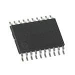
| 产品图片 |
|
| rohs | 符合RoHS无铅 / 符合限制有害物质指令(RoHS)规范要求 |
| 产品系列 | 接口 IC,数字隔离器,Analog Devices ADUM3482ARSZiCoupler® |
| 数据手册 | |
| 产品型号 | ADUM3482ARSZ |
| PulseWidthDistortion(Max) | 6ns |
| 上升/下降时间(典型值) | 2.5ns, 2.5ns |
| 产品种类 | |
| 传播延迟tpLH/tpHL(最大值) | 90ns, 90ns |
| 传播延迟时间 | 33 ns |
| 供应商器件封装 | 20-SSOP |
| 共模瞬态抗扰度(最小值) | 25kV/µs |
| 包装 | 管件 |
| 商标 | Analog Devices |
| 安装风格 | SMD/SMT |
| 封装 | Tube |
| 封装/外壳 | 20-SSOP(0.209",5.30mm 宽) |
| 封装/箱体 | SSOP-20 |
| 工作温度 | -40°C ~ 125°C |
| 工厂包装数量 | 66 |
| 技术 | 磁耦合 |
| 数据速率 | 1Mbps |
| 最大功率耗散 | 2470 mW |
| 最大工作温度 | + 125 C |
| 最大数据速率 | 1 Mb/s |
| 最小工作温度 | - 40 C |
| 标准包装 | 66 |
| 电压-电源 | 1.8 V ~ 5.5 V,3 V ~ 5.5 V |
| 电压-隔离 | 3750Vrms |
| 电源电压-最大 | 5.5 V |
| 电源电流 | 0.6 mA |
| 类型 | General Purpose |
| 系列 | ADUM3482 |
| 绝缘电压 | 3.75 kVrms |
| 脉宽失真(最大) | 6ns |
| 视频文件 | http://www.digikey.cn/classic/video.aspx?PlayerID=1364138032001&width=640&height=505&videoID=2219593469001http://www.digikey.cn/classic/video.aspx?PlayerID=1364138032001&width=640&height=505&videoID=2219593470001http://www.digikey.cn/classic/video.aspx?PlayerID=1364138032001&width=640&height=505&videoID=2219614223001 |
| 输入-输入侧1/输入侧2 | 2/2 |
| 通道数 | 4 |
| 通道数量 | 4 Channel |
| 通道类型 | 单向 |
| 隔离式电源 | 无 |


- 商务部:美国ITC正式对集成电路等产品启动337调查
- 曝三星4nm工艺存在良率问题 高通将骁龙8 Gen1或转产台积电
- 太阳诱电将投资9.5亿元在常州建新厂生产MLCC 预计2023年完工
- 英特尔发布欧洲新工厂建设计划 深化IDM 2.0 战略
- 台积电先进制程称霸业界 有大客户加持明年业绩稳了
- 达到5530亿美元!SIA预计今年全球半导体销售额将创下新高
- 英特尔拟将自动驾驶子公司Mobileye上市 估值或超500亿美元
- 三星加码芯片和SET,合并消费电子和移动部门,撤换高东真等 CEO
- 三星电子宣布重大人事变动 还合并消费电子和移动部门
- 海关总署:前11个月进口集成电路产品价值2.52万亿元 增长14.8%


PDF Datasheet 数据手册内容提取
Small, 3.75 kV RMS Quad Digital Isolators Data Sheet ADuM3480/ADuM3481/ADuM3482 FEATURES FUNCTIONAL BLOCK DIAGRAMS Up to 25 Mbps data rate (NRZ) ADuM3480 Low propagation delay: 25 ns typical VDDL1 1 20VDDL2 Low dynamic power consumption GND1 2 19GND2 1.8 V to 5 V level translation VIA 3 ENCODE DECODE 18VOA High temperature operation: 125°C High common-mode transient immunity: >25 kV/µs VIB 4 ENCODE DECODE 17VOB Output default select VIC 5 ENCODE DECODE 16VOC 20-lead, RoHS-compliant, SSOP package VID 6 ENCODE DECODE 15VOD Safety and regulatory approvals: NC 7 14CTRL2 UL recognition: 3750 V rms for 1 minute per UL 1577 VDD1 8 REG REG 13VDD2 CSA Component Acceptance Notice #5A VDDC1 9 12VDDC2 VDDEI cNe Vrt VifiDcEat Ve 0o8f 8co4n-1f0o r(mVDitEy V 0884-10):2006-12 GND110 11GND2 10459-001 VIORM = 560 V peak Figure 1. ADuM3480 APPLICATIONS ADuM3481 General-purpose multichannel isolation VDDL1 1 20VDDL2 SPI interface/data converter isolation GND1 2 19GND2 Industrial field bus isolation VIA 3 ENCODE DECODE 18VOA GENERAL DESCRIPTION VIB 4 ENCODE DECODE 17VOB The ADuM3480/ADuM3481/ADuM34821 are quad-channel VIC 5 ENCODE DECODE 16VOC digital isolators based on the Analog Devices, Inc., iCoupler® VOD 6 DECODE ENCODE 15VID technology. Combining high speed CMOS and monolithic air CTRL1 7 14CTRL2 core transformer technology, these isolation components provide VDD1 8 REG REG 13VDD2 outstanding performance characteristics superior to alternatives VDDC1 9 12VDDC2 styupcihc aals porpotpoacgoautpiolenr ddeelvayic reesd auncde do tthoe 2r 5in ntse,g prautlesde wcoiudtphle rs. With GND110 11GND2 10459-002 distortion is also halved. Figure 2. ADuM3481 The four channels of the ADuM3480/ADuM3481/ADuM3482 ADuM3482 are available in a variety of channel configurations with two data VDDL1 1 20VDDL2 rate grades up to 25 Mbps (see the Ordering Guide section). All GND1 2 19GND2 models use separate core and I/O power supplies. The core VIA 3 ENCODE DECODE 18VOA operates between 3.0 V and 5.5 V, whereas the I/O supply can VIB 4 ENCODE DECODE 17VOB range from 1.8 V to 5.5 V. If I/O operation is required within the range of the core supply, the two supplies can be tied together VOC 5 DECODE ENCODE 16VIC to allow single-supply operation. When the I/O must interface VOD 6 DECODE ENCODE 15VID with logic levels that are different from the core supply voltage, CTRL1 7 14CTRL2 the I/O supply operates independently of the core supply over VDD1 8 REG REG 13VDD2 its wider range. The minimum I/O supply voltage is 1.8 V, which VDDC1 9 12VDDC2 saullpopwlsie cso amrep raetqibuiilriteyd w foitrh p lroowp evro oltpaegrea ltoiognic.. Both core and I/O GND110 11GND2 10459-003 Figure 3. ADuM3482 1 Protected by U.S. Patents 5,952,849; 6,873,065; 6,903,578; and 7,075,329. Other patents are pending. Rev. A Document Feedback Information furnished by Analog Devices is believed to be accurate and reliable. However, no responsibility is assumed by Analog Devices for its use, nor for any infringements of patents or other One Technology Way, P.O. Box 9106, Norwood, MA 02062-9106, U.S.A. rights of third parties that may result from its use. Specifications subject to change without notice. No license is granted by implication or otherwise under any patent or patent rights of Analog Devices. Tel: 781.329.4700 ©2012–2014 Analog Devices, Inc. All rights reserved. Trademarks and registered trademarks are the property of their respective owners. Technical Support www.analog.com
ADuM3480/ADuM3481/ADuM3482 Data Sheet TABLE OF CONTENTS Features .............................................................................................. 1 Recommended Operating Conditions .................................... 10 Applications ....................................................................................... 1 Absolute Maximum Ratings ......................................................... 11 General Description ......................................................................... 1 ESD Caution................................................................................ 11 Functional Block Diagrams ............................................................. 1 Pin Configurations and Function Descriptions ......................... 12 Revision History ............................................................................... 2 Typical Performance Characteristics ........................................... 15 Specifications ..................................................................................... 3 Applications Information .............................................................. 17 Electrical Characteristics—5 V Operation................................ 3 Supply Voltages ........................................................................... 17 Electrical Characteristics—3 V Operation................................ 5 Printed Circuit Board Layout ................................................... 17 Electrical Characteristics—1.8 V Operation ............................ 7 Propagation Delay Related Parameters ................................... 17 Package Characteristics ............................................................... 9 DC Correctness and Magnetic Field Immunity ..................... 17 Regulatory Information ............................................................... 9 Power Consumption .................................................................. 18 Regulatory Approvals ................................................................... 9 Insulation Lifetime ..................................................................... 19 Insulation and Safety Related Specifications ............................ 9 Outline Dimensions ....................................................................... 20 DIN V VDE V 0884-10 (VDE V 0884-10) Insulation Ordering Guide .......................................................................... 20 Characteristics ............................................................................ 10 REVISION HISTORY 6/14—Rev. 0 to Rev. A Changed Safety Certification Status from Pending to Approved (Throughout) .................................................................................... 1 Changes to Table 12 .......................................................................... 9 Changed Highest Allowable Overvoltage from 5300 V to PEAK 4000 V ........................................................................................ 10 PEAK Changes to DC Correctness and Magnetic Field Immunity Section .............................................................................................. 17 Changes to Ordering Guide .......................................................... 20 7/12—Revision 0: Initial Version Rev. A | Page 2 of 20
Data Sheet ADuM3480/ADuM3481/ADuM3482 SPECIFICATIONS ELECTRICAL CHARACTERISTICS—5 V OPERATION All typical specifications are at T = 25°C, V = V = V = V = 5 V. Minimum/maximum specifications apply over the entire A DDL1 DD1 DDL2 DD2 recommended operation range: 4.5 V ≤ V , V ≤ 5.5 V, 4.5 V ≤ V , V ≤ 5.5 V, −40°C ≤ T ≤ +125°C, unless otherwise noted. DDL1 DD1 DDL2 DD2 A Switching specifications are tested with C = 15 pF, and CMOS signal levels, unless otherwise noted. L Table 1. A Grade B Grade Parameter Symbol Min Typ Max Min Typ Max Unit Test Conditions/Comments SWITCHING SPECIFICATIONS Pulse Width PW 1000 40 ns Within PWD limit Data Rate 1 25 Mbps Within PWD limit Propagation Delay t , t 65 90 25 33 ns 50% input to 50% output PHL PLH Pulse Width Distortion PWD 6 3 ns |t − t | PLH PHL Change vs. Temperature 7 3 ps/°C Propagation Delay Skew t 50 17 ns Between any two units PSK Channel Matching Codirectional t 19 5 ns PSKCD Opposing Direction t 25 7 ns PSKOD Jitter 2 2 ns Table 2. 1 Mbps—A, B Grades 25 Mbps—B Grade Parameter Symbol Min Typ Max Min Typ Max Unit Test Conditions/Comments SUPPLY CURRENT ADuM3480 I 2.0 2.9 8.6 12 mA DD1 I 0.11 0.4 0.2 0.6 mA DDL1 I 5.1 6.9 6.0 7.5 mA DD2 I 0.2 0.7 2.1 4.8 mA C = 0 pF DDL2 L ADuM3481 I 2.8 3.0 7.9 10 mA DD1 I 0.14 0.5 0.7 1.4 mA C = 0 pF DDL1 L I 4.3 5.7 6.7 7.8 mA DD2 I 0.18 0.6 1.6 3.2 mA C = 0 pF DDL2 L ADuM3482 I 3.5 4.1 7.3 8.8 mA DD1 I 0.16 0.5 1.2 2.4 mA C = 0 pF DDL1 L I 3.5 4.7 7.3 8.8 mA DD2 I 0.16 0.65 1.2 2.4 mA C = 0 pF DDL2 L Rev. A | Page 3 of 20
ADuM3480/ADuM3481/ADuM3482 Data Sheet Table 3. Parameter Symbol Min Typ Max Unit Test Conditions/Comments DC SPECIFICATIONS Input Voltage Threshold Logic High V 0.7 V V IH DDLx Logic Low V 0.3 V V IL DDLx Output Voltages Logic High V V − 0.1 5.0 V I = −20 µA, V = V OH DDLx Ox Ix IxH V − 0.4 4.8 V I = −4 mA, V = V DDLx Ox Ix IxH Logic Low V 0.0 0.1 V I = 20 µA, V = V OL Ox Ix IxL 0.2 0.4 V I = 4 mA, V = V Ox Ix IxL Input Current per Channel I −10 +0.01 +10 µA 0 V ≤ V ≤ V , 0 V ≤ V ≤ V I Ix DDLx CTRLx DDLx Supply Current per Channel Quiescent Supply Current Regulator Input Side I 0.50 0.60 mA DDI (Q) I/O Input I 0.027 0.05 mA DDIL (Q) Regulator Output Side I 1.26 1.7 mA DDO (Q) I/O Output I 0.031 0.10 mA DDOL (Q) Dynamic Supply Current Regulator Input Side I 0.070 mA/Mbps DDI (D) I/O Input I 0.90 µA/Mbps DDIL (D) Regulator Output Side I 0.010 mA/Mbps DDO (D) I/O Output I 0.020 mA/Mbps DDOL (D) AC SPECIFICATIONS Output Rise/Fall Time t /t 2.5 ns 10% to 90% R F Common-Mode Transient Immunity1 |CM| 25 35 kV/µs V = V , V = 1000 V, transient Ix DDLx CM magnitude = 800 V Refresh Period t 1.66 µs r 1 |CM| is the maximum common-mode voltage slew rate that can be sustained while maintaining VOL < 0.8 × VDDLx or VOH > 0.7 × VDDIx. The common-mode voltage slew rates apply to both rising and falling common-mode voltage edges. Rev. A | Page 4 of 20
Data Sheet ADuM3480/ADuM3481/ADuM3482 ELECTRICAL CHARACTERISTICS—3 V OPERATION All typical specifications are at T = 25°C, V = V = V = V = 3.0 V. Minimum/maximum specifications apply over the entire A DDL1 DD1 DDL2 DD2 recommended operation range: 3.0 V ≤ V ,V ≤ 3.6 V, 3.0 V ≤ V , V ≤ 3.6 V, −40°C ≤ T ≤ +125°C, unless otherwise noted. DDL1 DD1 DDL2 DD2 A Switching specifications are tested with C = 15 pF and CMOS signal levels, unless otherwise noted. L Table 4. A Grade B Grade Parameter Symbol Min Typ Max Min Typ Max Unit Test Conditions/Comments SWITCHING SPECIFICATIONS Pulse Width PW 1000 40 ns Within PWD limit Data Rate 1 25 Mbps Within PWD limit Propagation Delay t , t 71 99 28 38 ns 50% input to 50% output PHL PLH Pulse Width Distortion PWD 2 12 3 5 ns |t − t | PLH PHL Change vs. Temperature 7 3 ps/°C Propagation Delay Skew t 58 20 ns Between any two units PSK Channel Matching Codirectional t 20 6 ns PSKCD Opposing Direction t 26 9 ns PSKOD Jitter 4 3 ns Table 5. 1 Mbps—A, B Grades 25 Mbps—B Grade Parameter Symbol Min Typ Max Min Typ Max Unit Test Conditions/Comments SUPPLY CURRENT ADuM3480 I 1.4 2.9 8.1 11 mA DD1 I 0.08 0.4 0.13 0.5 mA DDL1 I 4.9 6.7 5.8 7.2 mA DD2 I 0.14 0.40 1.4 2.5 mA C = 0 pF DDL2 L ADuM3481 I 2.3 3.0 7.5 9.8 mA DD1 I 0.09 0.4 0.46 1.4 mA C = 0 pF DDL1 L I 4.0 5.7 6.4 7.5 mA DD2 I 0.12 0.5 1.1 2.7 mA C = 0 pF DDL2 L ADuM3482 I 3.2 4.2 7.0 8.8 mA DD1 I 0.11 0.5 0.78 1.7 mA C = 0 pF DDL1 L I 3.2 4.2 7.0 8.8 mA DD2 I 0.11 0. 5 0.78 1.7 mA C = 0 pF DDL2 L Rev. A | Page 5 of 20
ADuM3480/ADuM3481/ADuM3482 Data Sheet Table 6. Parameter Symbol Min Typ Max Unit Test Conditions/Comments DC SPECIFICATIONS Input Voltage Threshold Logic High V 0.7 V V IH DDLx Logic Low V 0.3 V V IL DDLx Output Voltages Logic High V V − 0.1 3.0 V I = −20 µA, V = V OH DDLx Ox Ix IxH V − 0.4 2.8 V I = −4 mA, V = V DDLx Ox Ix IxH Logic Low V 0.0 0.1 V I = 20 µA, V = V OL Ox Ix IxL 0.2 0.4 V I = 4 mA, V = V Ox Ix IxL Input Current per Channel I −10 +0.01 +10 µA 0 V ≤ V ≤ V , 0 V ≤ V ≤ V I Ix DDLx CTRLx DDLx Supply Current per Channel Quiescent Supply Current Regulator Input Side I 0.36 0.5 mA DDI (Q) I/O Input I 0.019 0.050 mA DDIL (Q) Regulator Output Side I 1.21 1.7 mA DDO (Q) I/O Output I 0.021 0.050 mA DDOL (Q) Dynamic Supply Current Regulator Input Side I 0.070 mA/Mbps DDI (D) I/O Input I 0.53 µA/Mbps DDIL (D) Regulator Output Side I 0.010 mA/Mbps DDO (D) I/O Output I 0.013 mA/Mbps DDOL (D) AC SPECIFICATIONS Output Rise/Fall Time t /t 3 ns 10% to 90% R F Common-Mode Transient Immunity1 |CM| 25 35 kV/µs V = V , V = 1000 V, Ix DDLx CM transient magnitude = 800 V Refresh Period t 1.66 µs r 1 |CM| is the maximum common-mode voltage slew rate that can be sustained while maintaining VOL < 0.8 × VDDLx or VOH > 0.7 × VDDIx. The common-mode voltage slew rates apply to both rising and falling common-mode voltage edges. Rev. A | Page 6 of 20
Data Sheet ADuM3480/ADuM3481/ADuM3482 ELECTRICAL CHARACTERISTICS—1.8 V OPERATION All typical specifications are at T = 25°C, V = 1.8 V, V = 3.0 V, V = 1.8 V, V = 3.0 V. Minimum/maximum specifications A DDL1 DD1 DDL2 DD2 apply over the entire recommended operation range: V = 1.8 V, 3.0 V ≤ V ≤ 3.6 V, V = 1.8 V, 3.0 V ≤ V ≤ 3.6 V,−40°C ≤ T ≤ DDL1 DD1 DDL2 DD2 A +125°C; unless otherwise noted. Switching specifications are tested with C = 15 pF and CMOS signal levels, unless otherwise noted. L Table 7. A Grade B Grade Parameter Symbol Min Typ Max Min Typ Max Unit Test Conditions/Comments SWITCHING SPECIFICATIONS Pulse Width PW 1000 40 ns Within PWD limit Data Rate 1 25 Mbps Within PWD limit Propagation Delay t , t 86 145 43 85 ns 50% input to 50% output PHL PLH Pulse Width Distortion PWD 6 32 6 30 ns |t − t | PLH PHL Change vs. Temperature 7 3 ps/°C Propagation Delay Skew t 93 60 ns Between any two units PSK Channel Matching Codirectional t 40 34 ns PSKCD Opposing Direction t 55 37 ns PSKOD Jitter 4 3 ns Table 8. 1 Mbps—A, B Grades 25 Mbps—B Grade Parameter Symbol Min Typ Max Min Typ Max Unit Test Conditions/Comments SUPPLY CURRENT ADuM3480 I 1.4 1.9 8.1 11 mA DD1 I 0.04 0.3 0.07 0.4 mA DDL1 I 4.7 6.5 5.7 7.3 mA DD2 I 0.08 0.5 0.82 1.5 mA C = 0 pF DDL2 L ADuM3481 I 2.3 2.8 7.5 10 mA DD1 I 0.05 0.35 0.25 0.7 mA C = 0 pF DDL1 L I 3.9 5.7 6.3 8.0 mA DD2 I 0.07 0.4 0.63 1.3 mA C = 0 pF DDL2 L ADuM3482 I 3.1 3.8 6.9 8.7 mA DD1 I 0.06 0.4 0.44 1.1 mA C = 0 pF DDL1 L I 3.1 4.5 6.9 8.8 mA DD2 I 0.06 0.40 0.44 1.1 mA C = 0 pF DDL2 L Rev. A | Page 7 of 20
ADuM3480/ADuM3481/ADuM3482 Data Sheet Table 9. Parameter Symbol Min Typ Max Unit Test Conditions/Comments DC SPECIFICATIONS Input Voltage Threshold Logic High V 0.7 V V IH DDLx Logic Low V 0.3 V V IL DDLx Output Voltages Logic High V V − 0.1 1.8 V I = −20 µA, V = V OH DDLx Ox Ix IxH V − 0.4 1.6 V I = −2 mA, V = V DDLx Ox Ix IxH Logic Low V 0.0 0.1 V I = 20 µA, V = V OL Ox Ix IxL 0.2 0.4 V I = 2 mA, V = V Ox Ix IxL Input Current per Channel I −10 +0.01 +10 µA 0 V ≤ V ≤ V , 0 V ≤ V ≤ V I Ix DDLx CTRLx DDLx Supply Current per Channel Quiescent Supply Current Regulator Input Side I 0.39 0.45 mA DDI (Q) I/O Input I 0.010 0.025 mA DDIL (Q) Regulator Output Side I 1.17 1.5 mA DDO (Q) I/O Output I 0.012 0.038 mA DDOL (Q) Dynamic Supply Current Regulator Input Side I 0.071 mA/Mbps DDI (D) I/O Input I 0.25 µA/Mbps DDIL (D) Regulator Output Side I 0.010 mA/Mbps DDO (D) I/O Output I 0.0077 mA/Mbps DDOL (D) AC SPECIFICATIONS Output Rise/Fall Time t /t 3 ns 10% to 90% R F Common-Mode Transient Immunity1 |CM| 25 35 kV/µs V = V , V = 1000 V, Ix DDLx CM transient magnitude = 800 V Refresh Period t 1.66 µs r 1 |CM| is the maximum common-mode voltage slew rate that can be sustained while maintaining VOL < 0.8 × VDDLx or VOH > 0.7 × VDDIx. The common-mode voltage slew rates apply to both rising and falling common-mode voltage edges. Rev. A | Page 8 of 20
Data Sheet ADuM3480/ADuM3481/ADuM3482 PACKAGE CHARACTERISTICS Table 10. Parameter Symbol Min Typ Max Unit Test Conditions/Comments Resistance (Input-to-Output)1 R 1012 Ω I-O Capacitance (Input-to-Output)1 C 2.2 pF f = 1 MHz I-O Input Capacitance2 C 4.0 pF I IC Junction-to-Case Thermal Resistance θ 50.5 °C/W Thermocouple located at center of package underside, JC test conducted on 4-layer board with thin traces 1 The device is considered a 2-terminal device: Pin 1 to Pin 10 are shorted together; Pin 11 to Pin 20 are shorted together. 2 Input capacitance is from any input data pin to ground. REGULATORY INFORMATION The ADuM3480/ADuM3481/ADuM3482 are approved by the organizations listed in Table 11. See Table 16 and the Insulation Lifetime section for the recommended maximum working voltages for specific cross-isolation waveforms and insulation levels. REGULATORY APPROVALS Table 11. UL CSA VDE Recognized under the UL 1577 Approved under CSA Component Certified according to DIN V VDE V 0884-10 component recognition program1 Acceptance Notice #5A (VDE V 0884-10):2006-122 Single protection, 3750 V rms Basic insulation per CSA 60950-1-03 and Reinforced insulation, 560 V peak isolation voltage IEC 60950-1, 400 V rms (565 V peak) maximum working voltage File E214100 File 205078 File 2471900-4880-0001 1 In accordance with UL 1577, each ADuM3480/ADuM3481/ADuM3482 is proof tested by applying an insulation test voltage of ≥4500 V rms for 1 second (current leakage detection limit = 10 µA). 2 In accordance with DIN V VDE V 0884-10, each of the ADuM348x is proof tested by applying an insulation test voltage of ≥1050 V peak for 1 second (partial discharge detection limit = 5 pC). The asterisk (*) marking branded on the component designates DIN V VDE V 0884-10 approval. INSULATION AND SAFETY RELATED SPECIFICATIONS Table 12. Parameter Symbol Value Unit Test Conditions/Comments Rated Dielectric Insulation Voltage 3750 V rms 1-minute duration Minimum External Air Gap (Clearance) L(I01) >5.1 mm Measured from input terminals to output terminals, shortest distance through air, in the plane of the PCB Minimum External Tracking (Creepage) L(I02) >5.1 mm Measured from input terminals to output terminals, shortest distance path along body Minimum Internal Gap (Internal Clearance) 0.017 min mm Distance through insulation Tracking Resistance (Comparative Tracking Index) CTI >400 V DIN IEC 112/VDE 0303 Part 1 Isolation Group II Material Group (DIN VDE 0110, 1/89, Table 1) Rev. A | Page 9 of 20
ADuM3480/ADuM3481/ADuM3482 Data Sheet DIN V VDE V 0884-10 (VDE V 0884-10):2006-12 INSULATION CHARACTERISTICS These isolators are suitable for reinforced electrical isolation only within the safety limit data. Maintenance of the safety data is ensured by protective circuits. The asterisk (*) marking on packages denotes DIN V VDE V 0884-10 approval. Table 13. Description Test Conditions/Comments Symbol Characteristic Unit Installation Classification per DIN VDE 0110 For Rated Mains Voltage ≤ 150 V rms I to IV For Rated Mains Voltage ≤ 300 V rms I to III For Rated Mains Voltage ≤ 400 V rms I to II Climatic Classification 40/105/21 Pollution Degree per DIN VDE 0110, Table 1 2 Maximum Working Insulation Voltage V 560 V IORM PEAK Input-to-Output Test Voltage, Method B1 V × 1.875 = V , 100% production test, t = t = V 1050 V IORM pd(m) ini m pd(m) PEAK 1 sec, partial discharge < 5 pC Input-to-Output Test Voltage, Method A After Environmental Tests Subgroup 1 V × 1.5 = V , t = 60 sec, t = 10 sec, partial V 840 V IORM pd(m) ini m pd(m) PEAK discharge < 5 pC After Input and/or Safety Test Subgroup 2 V × 1.2 = V , t = 60 sec, t = 10 sec, partial V 672 V IORM pd(m) ini m pd(m) PEAK and Subgroup 3 discharge < 5 pC Highest Allowable Overvoltage V 4000 V IOTM PEAK Withstand Isolation Voltage 1 minute withstand rating V 3750 V ISO RMS Surge Isolation Voltage V = 10 kV, 1.2 µs rise time, 50 µs, 50% fall time V 6000 V PEAK IOSM PEAK Safety Limiting Values Maximum value allowed in the event of a failure (see Figure 4) Case Temperature T 150 °C S Total Power Dissipation I 2.47 W S1 Insulation Resistance at T V = 500 V R >109 Ω S IO S RECOMMENDED OPERATING CONDITIONS 3.0 Table 14. 2.5 W) Parameter Symbol Min Max Unit R ( WE 2.0 Operating Temperature TA −40 +125 °C O Supply Voltages1 V , V 1.8 5.5 V P DDL1 DDL2 TING 1.5 VDD1, VDD2 3.0 5.5 V MI Input Signal Rise and Fall 1.0 ms TY-LI 1.0 Times FE 1 See the DC Correctness and Magnetic Field Immunity section for information A S on immunity to external magnetic fields. 0.5 00 50AMBIENT TEM1P00ERATURE (°C1)50 200 10459-004 Figure 4. Thermal Derating Curve, Dependence of Safety Limiting Values with Ambient Temperature per DIN V VDE V 0884-10 Rev. A | Page 10 of 20
Data Sheet ADuM3480/ADuM3481/ADuM3482 ABSOLUTE MAXIMUM RATINGS T = 25°C, unless otherwise noted. Table 16. Maximum Continuous Working Voltage A Supporting 50-Year Minimum Lifetime1 Table 15. Applicable Parameter Rating Parameter Max Unit Certification Supply Voltages (VDD1, VDD2, VDDL1, −0.5 V to +7.0 V AC Voltage, Bipolar 565 V peak All certifications VDDL2, VDDC1, VDDC2) Waveform Input Voltages (VIA, VIB, VIC, VID, VCTRL1, −0.5 V to VDDI + 0.5 V AC Voltage, Unipolar 848 V peak VCTRL2) Waveform Output Voltages (VOA, VOB, VOC, VOD) −0.5 V to VDDO + 0.5 V DC Voltage 848 V peak Average Output Current per Pin1 −10 mA to +10 mA Common-Mode Transients2 −100 kV/μs to +100 kV/μs 1 Refers to the continuous voltage magnitude imposed across the isolation barrier. See the Insulation Lifetime section for more information. Storage Temperature (T ) Range −65°C to +150°C ST ESD CAUTION Ambient Operating Temperature −40°C to +125°C (T ) Range A 1 See Figure 4 for maximum rated current values for various temperatures. 2 Refers to common-mode transients across the insulation barrier. Common- mode transients exceeding the absolute maximum ratings may cause latch-up or permanent damage. Stresses above those listed under Absolute Maximum Ratings may cause permanent damage to the device. This is a stress rating only; functional operation of the device at these or any other conditions above those indicated in the operational section of this specification is not implied. Exposure to absolute maximum rating conditions for extended periods may affect device reliability. Rev. A | Page 11 of 20
ADuM3480/ADuM3481/ADuM3482 Data Sheet PIN CONFIGURATIONS AND FUNCTION DESCRIPTIONS VDDL1 1 20 VDDL2 GND1* 2 19 GND2* VIA 3 18 VOA VIB 4 ADuM3480 17 VOB VIC 5 TOP VIEW 16 VOC (Not to Scale) VID 6 15 VOD NC 7 14 CTRL2 VDD1 8 13 VDD2 VDDC1 9 12 VDDC2 GND1* 10 11 GND2* NOTES 1. NC = NO CONNECTION. THIS PIN IS NOT CONNECTED INTERNALLY AND CAN BE LEFT FLOATING OR CONNECTED TO VDD1 OR GND1. *PIN 2 AND PIN 10 ARE INTERNALLY CONNECTED. CONNECTING BOTH TO PCB SIDE 1 GROUND IS RITNOETC EPORCMNBMA SLEILDNYED EC2 DOG.N RPNOIENUC 1NT1DE A DISN. DCR OEPCNINON 1ME9CM ATERINNEGDE BDO.TH 10459-005 Figure 5. ADuM3480 Pin Configuration Table 17. ADuM3480 Pin Function Descriptions Pin No. Mnemonic Description 1 V 1.8 V to 5.5 V Supply Voltage for Isolator Side 1 Input/Output Circuits. Bypass V to GND with a 0.01 µF to 0.1 µF DDL1 DDL1 1 ceramic capacitor. For 3.0 V to 5.5 V input/output operation, V can be connected directly to V . DDL1 DD1 2 GND Ground 1. Ground reference for Isolator Side 1. Pin 2 and Pin 10 are internally connected, and connecting both to 1 the PCB ground plane as close to the part as possible is recommended. 3 V Logic Input A. IA 4 V Logic Input B. IB 5 V Logic Input C. IC 6 V Logic Input D. ID 7 NC No Connection. This pin is not connected internally and can be left floating or connected to V or GND. DD1 1 8 V 3.0 V to 5.5 V Supply Voltage for Isolator Side 1. DD1 9 V Output Pin of an Internal Regulator for Side 1. Bypass V to GND with a 0.01 µF to 0.1 µF ceramic capacitor. Do DDC1 DDC1 1 not use this pin to power external circuits. 10 GND Ground 1. Ground reference for Isolator Side 1. Pin 2 and Pin 10 are internally connected, and connecting both to 1 the PCB ground plane as close to the part as possible is recommended. 11 GND Ground 2. Ground reference for Isolator Side 2. Pin 11 and Pin 19 are internally connected, and connecting both to 2 the PCB ground plane as close to the part as possible is recommended. 12 V Output Pin of an Internal Regulator for Side 2. Bypass V to GND with a 0.01 µF to 0.1 µF ceramic capacitor. Do DDC2 DDC2 2 not use this pin to power external circuits. 13 V 3.0 V to 5.5 V Supply Voltage for Isolator Side 2. DD2 14 CTRL Select Side 2 Output Default Level. Low = default output low. High = default output high. 2 15 V Logic Output D. OD 16 V Logic Output C. OC 17 V Logic Output B. OB 18 V Logic Output A. OA 19 GND Ground 2. Ground reference for Isolator Side 2. Pin 11 and Pin 19 are internally connected, and connecting both to 2 the PCB ground plane as close to the part as possible is recommended. 20 V 1.8 V to 5.5 V Supply Voltage for Isolator Side 2 Input/Output Circuits. Bypass V to GND with a 0.01 µF to 0.1 µF DDL2 DDL2 2 ceramic capacitor. For 3.0 V to 5.5 V input/output operation, V can be connected directly to V . DDL2 DD2 Rev. A | Page 12 of 20
Data Sheet ADuM3480/ADuM3481/ADuM3482 VDDL1 1 20 VDDL2 GND1* 2 19 GND2* VIA 3 18 VOA VIB 4 ADuM3481 17 VOB VIC 5 TOP VIEW 16 VOC (Not to Scale) VOD 6 15 VID CTRL1 7 14 CTRL2 VDD1 8 13 VDD2 VDDC1 9 12 VDDC2 GND1* 10 11 GND2* *PIN 2 AND PIN 10 ARE INTERNALLY CONNECTED. CONNECTING BOTH TO PCB SIDE 1 GROUND IS RITNOETC EPORCMNBMA SLEILDNYED EC2 DOG.N RPNOIENUC 1NT1DE A DISN. DCR OEPCNINON 1ME9CM ATERINNEGDE BDO.TH 10459-006 Figure 6. ADuM3481 Pin Configuration Table 18. ADuM3481 Pin Function Descriptions Pin No. Mnemonic Description 1 V 1.8 V to 5.5 V Supply Voltage for Isolator Side 1 Input/Output Circuits. Bypass V to GND with a 0.01 µF to 0.1 µF DDL1 DDL1 1 ceramic capacitor. For 3.0 V to 5.5 V input/output operation, V can be connected directly to V . DDL1 DD1 2 GND Ground 1. Ground reference for Isolator Side 1. Pin 2 and Pin 10 are internally connected, and connecting both to 1 the PCB ground plane as close to the part as possible is recommended. 3 V Logic Input A. IA 4 V Logic Input B. IB 5 V Logic Input C. IC 6 V Logic Output D. OD 7 CTRL Select Side 1 Output Default Level. Low = default output low. High = default output high. 1 8 V 3.0 V to 5.5 V Supply Voltage for Isolator Side 1. DD1 9 V Output Pin of an Internal Regulator for Side 1. Bypass V to GND with a 0.01 µF to 0.1 µF ceramic capacitor. Do DDC1 DDC1 1 not use this pin to power external circuits. 10 GND Ground 1. Ground reference for Isolator Side 1. Pin 2 and Pin 10 are internally connected, and connecting both to 1 the PCB ground plane as close to the part as possible is recommended. 11 GND Ground 2. Ground reference for Isolator Side 2. Pin 11 and Pin 19 are internally connected, and connecting both to 2 the PCB ground plane as close to the part as possible is recommended. 12 V Output Pin of an Internal Regulator for Side 2. Bypass V to GND with a 0.01 µF to 0.1 µF ceramic capacitor. Do DDC2 DDC2 2 not use this pin to power external circuits. 13 V 3.0 V to 5.5 V Supply Voltage for Isolator Side 2. DD2 14 CTRL Select Side 2 Output Default Level. Low = default output low. High = default output high. 2 15 V Logic Input D. ID 16 V Logic Output C. OC 17 V Logic Output B. OB 18 V Logic Output A. OA 19 GND Ground 2. Ground reference for Isolator Side 2. Pin 11 and Pin 19 are internally connected, and connecting both to 2 the PCB ground plane as close to the part as possible is recommended. 20 V 1.8 V to 5.5 V Supply Voltage for Isolator Side 2 Input/Output Circuits. Bypass V to GND with a 0.01 µF to 0.1 µF DDL2 DDL2 2 ceramic capacitor. For 3.0 V to 5.5 V input/output operation, V can be connected directly to V . DDL2 DD2 Rev. A | Page 13 of 20
ADuM3480/ADuM3481/ADuM3482 Data Sheet VDDL1 1 20 VDDL2 GND1* 2 19 GND2* VIA 3 18 VOA VIB 4 ADuM3482 17 VOB VOC 5 TOP VIEW 16 VIC (Not to Scale) VOD 6 15 VID CTRL1 7 14 CTRL2 VDD1 8 13 VDD2 VDDC1 9 12 VDDC2 GND1* 10 11 GND2* *PIN 2 AND PIN 10 ARE INTERNALLY CONNECTED. CONNECTING BOTH TO PCB SIDE 1 GROUND IS RITNOETC EPORCMNBMA SLEILDNYED EC2 DOG.N RPNOIENUC 1NT1DE A DISN. DCR OEPCNINON 1ME9CM ATERINNEGDE BDO.TH 10459-007 Figure 7. ADuM3482 Pin Configuration Table 19. ADuM3482 Pin Function Descriptions Pin No. Mnemonic Description 1 V 1.8 V to 5.5 V Supply Voltage for Isolator Side 1 Input/Output Circuits. Bypass V to GND with a 0.01 µF to 0.1 µF DDL1 DDL1 1 ceramic capacitor. For 3.0 V to 5.5 V input/output operation, V can be connected directly to V . DDL1 DD1 2 GND Ground 1. Ground reference for Isolator Side 1. Pin 2 and Pin 10 are internally connected, and connecting both to 1 the PCB ground plane as close to the part as possible is recommended. 3 V Logic Input A. IA 4 V Logic Input B. IB 5 V Logic Output C. OC 6 V Logic Output D. OD 7 CTRL Select Side 1 Output Default Level. Low = default output low. High = default output high. 1 8 V 3.0 V to 5.5 V Supply Voltage for Isolator Side 1. DD1 9 V Output Pin of Internal Regulator for Side 1. Bypass V to GND with a 0.01 µF to 0.1 µF ceramic capacitor. Do not DDC1 DDC1 1 use this pin to power external circuits. 10 GND Ground 1. Ground reference for Isolator Side 1. Pin 2 and Pin 10 are internally connected, and connecting both to 1 the PCB ground plane as close to the part as possible is recommended. 11 GND Ground 2. Ground reference for Isolator Side 2. Pin 11 and Pin 19 are internally connected, and connecting both to 2 the PCB ground plane as close to the part as possible is recommended. 12 V Output Pin of Internal Regulator for Side 2. Bypass V to GND with a 0.01 µF to 0.1 µF ceramic capacitor. Do not DDC2 DDC2 2 use this pin to power external circuits. 13 V 3.0 V to 5.5 V Supply Voltage for Isolator Side 2. DD2 14 CTRL Select Side 2 Output Default Level. Low = default output low. High = default output high. 2 15 V Logic Input D. ID 16 V Logic Input C. IC 17 V Logic Output B. OB 18 V Logic Output A. OA 19 GND Ground 2. Ground reference for Isolator Side 2. Pin 11 and Pin 19 are internally connected, and connecting both to 2 the PCB ground plane as close to the part as possible is recommended. 20 V 1.8 V to 5.5 V Supply Voltage for Isolator Side 2 Input/Output Circuits. Bypass V to GND with a 0.01 µF to 0.1 µF DDL2 DDL2 2 ceramic capacitor. For 3.0 V to 5.5 V input/output operation, V can be connected directly to V . DDL2 DD2 Rev. A | Page 14 of 20
Data Sheet ADuM3480/ADuM3481/ADuM3482 TYPICAL PERFORMANCE CHARACTERISTICS 2.5 1.6 1.4 VDD = 3.3V/VDDL = 1.8V A) 2.0 A) ANNEL (m 1.5 ANNEL (m 11..20 VDD = 3.3V/VDDL = 3.3V NT/CH VDD = 5V/VDDL = 1.8V VDD = 5V/VDDL = 5V NT/CH 0.8 RRE 1.0 RRE 0.6 CU CU I DDI 0.5 I DDO 0.4 0.2 00 5 DA1T0A RATE (M1b5ps) 20 25 10459-008 00 5 DA1T0A RATE (M1b5ps) 20 25 10459-011 Figure 8. Typical VDDI = 5 V Supply Current per Input Channel vs. Data Rate Figure 11. Typical VDDO = 3.3 V Supply Current per Output Channel vs. Data for 5 V and 1.8 V I/O Operation Rate for 3.3 V and 1.8 V I/O Operation 2.5 0.06 0.05 CURRENT/CHANNEL (mA)DI 211...050 VDD = 3.3V/VDDL = 1.8V CURRENT/CHANNEL (mA)DIL 000...000432 VVVDDDDDDLLL == = 31 5..38VVV ID 0.5 VD VDD = 3.3V/VDDL = 3.3V 0.01 00 5 DA1T0A RATE (M1b5ps) 20 25 10459-009 00 5 DA1T0A RATE (M1b5ps) 20 25 10459-012 Figure 9. Typical VDDI = 3.3 V Supply Current per Input Channel vs. Data Rate Figure 12. Typical VDDIL Input Supply Current vs. Data Rate for 5 V, 3.3 V, and for 3.3 V, and 1.8 V I/O Operation 1.8 V Operation 1.6 0.6 VDD = 5V/VDDL = 1.8V 1.4 0.5 I CURRENT/CHANNEL (mA)DDO 11000.....20864 VDD = 5V/VDDL = 5V I CURRENT/CHANNEL (mA)DDOL 0000....4321 VDDL = 5V VDDL = 3.3V 0.2 VDDL = 1.8V 00 5 DA1T0A RATE (M1b5ps) 20 25 10459-010 00 5 DA1T0A RATE (M1b5ps) 20 25 10459-013 Figure 10. Typical VDDO = 5 V Supply Current per Output Channel vs. Data Figure 13. Typical VDDOL Output Supply Current vs. Data Rate Rate for 5 V and 1.8 V I/O Operation for 5 V, 3.3 V, and 1.8 V, CL = 0 pF Operation Rev. A | Page 15 of 20
ADuM3480/ADuM3481/ADuM3482 Data Sheet 1.6 1.4 A) L (m 1.2 VDDL = 5V E N N 1.0 A H C T/ 0.8 EN VDDL = 3.3V R R 0.6 U CL VDDL = 1.8V O 0.4 D D I 0.2 00 5 DA1T0A RATE (M1b5ps) 20 25 10459-014 Figure 14. Typical VDDOL Output Supply Current vs. Data Rate for 5 V, 3.3 V, and 1.8 V, CL = 15 pF Operation Rev. A | Page 16 of 20
Data Sheet ADuM3480/ADuM3481/ADuM3482 APPLICATIONS INFORMATION SUPPLY VOLTAGES In applications involving high common-mode transients, it is important to minimize board coupling across the isolation barrier. The ADuM3480/ADuM3481/ADuM3482 devices are built Furthermore, design the board layout so that any coupling that around a fixed voltage internal data transfer core. The core does occur equally affects all pins on a given component side. voltage is 2.7 V, which is generated by regulating the V and DD1 Failure to follow this design guideline can allow voltage differentials V voltages with an internal LDO. To ensure proper headroom DD2 between pins that exceed the absolute maximum ratings of the for the LDO, the V and V inputs must be in the 3.0 V to 5.5 V DD1 DD2 device during high voltage transients, which can lead to latch-up or range. Additional pins, V and V , are provided for direct DDC1 DDC2 permanent damage. bypass of the LDO output, ensuring clean stable core operation. PROPAGATION DELAY RELATED PARAMETERS Bypass capacitors to ground of between 0.01 μF and 0.1 μF are required for each of these supply or dedicated bypass pins. Propagation delay is a parameter that describes the time it takes The ADuM3480/ADuM3481/ADuM3482 provide independent a logic signal to propagate through a component. The input-to- supplies for the I/O buffers, V and V , which have wider output propagation delay time for a high to low transition may DDL1 DDL2 differ from the propagation delay time of a low to high transition. operating ranges than that required for the core. This allows the I/O supply voltage to range between 1.8 V and 5.5 V. The V DDLx supplies must also be bypassed with between 0.01 μF and 0.1 μF INPUT (VIx) 50% capacitors. tPLH tPHL Hseavveirnagl pinodweepre cnodnefnigt uproawtieorn ssu dpeppleiensd fionrg t ohne It/hOe Ia/nOd vcoolrtea gael lows OUTPUT (VOx) 50% 10459-017 required and the available power supply rails. If one power Figure 16. Propagation Delay Parameters supply is available, the VDDx and VDDLx pins can be connected Pulse width distortion is the maximum difference between together and operate between 3.0 V and 5.5 V. If lower I/O these two propagation delay values and an indication of how supply voltage is required, to interface with low voltage logic, accurately the timing of the input signal is preserved. two supply rails are required. For example, if the I/O is 1.8 V Channel to channel matching refers to the maximum amount of logic, the V pin can be connected to a 1.8 V supply rail. The DDLx time that the propagation delay differs between channels within core supply voltage for V requires an input of between 3.0 V and DDx a single ADuM3480/ADuM3481/ADuM3482 component. 5.5 V, so an available 3.3 V or 5 V supply rail can be used. The I/O and core supply voltage on each side are independent and different Propagation delay skew refers to the maximum amount of time configurations can be used on each side of the device. that the propagation delay differs between multiple ADuM3480/ ADuM3481/ADuM3482 components operating under the same PRINTED CIRCUIT BOARD LAYOUT conditions. The ADuM3480/ADuM3481/ADuM3482 digital isolator requires DC CORRECTNESS AND MAGNETIC FIELD no external interface circuitry for the logic interfaces. Power supply IMMUNITY bypassing to the local ground is required at all four power supply pins, V , V , V , and V , as well as at the two internal Positive and negative logic transitions at the isolator input cause DD1 DDL1 DD2 DDL2 regulator bypass pins: V and V (see Figure 15). Placement narrow (~1 ns) pulses to be sent via the transformer to the decoder. DDC1 DDC2 of the recommended bypass capacitors is shown in Figure 15. The The decoder is bistable and is, therefore, either set or reset by capacitor value should be between 0.01 μF and 0.1 μF. The total lead the pulses indicating input logic transitions. In the absence of length between both ends of the capacitor and the input power logic transitions at the input for more than ~1.7 μs, the current supply pin should not exceed 20 mm. dc state is sent to the output to ensure dc correctness at the output. If the decoder receives no pulses for more than about 5 μs, the VDDL1 VDDL2 GND1 GND2 input side is assumed to be unpowered or nonfunctional, in which VIA VOA case the isolator output is forced to a default state (see Table 17, VIB VOB VIC/VOC VOC/VIC Table 18, or Table 19) by the watchdog timer circuit. VID/VOD VOD/VID CTRL1 CTRL2 VGVDNDDDCD111 VVGDDNDDD2C22 10459-016 Figure 15. Recommended Printed Circuit Board (PCB) Layout Rev. A | Page 17 of 20
ADuM3480/ADuM3481/ADuM3482 Data Sheet The limitation on the magnetic field immunity of the device is set The preceding magnetic flux density values correspond to by the condition in which induced voltage in the receiving coil specific current magnitudes at given distances away from the of the transformer is sufficiently large to either falsely set or ADuM3480/ADuM3481/ADuM3482 transformers. Figure 18 reset the decoder. The following analysis defines such conditions. expresses these allowable current magnitudes as a function of The ADuM3480/ADuM3481/ADuM3482 are examined in a frequency for selected distances. The ADuM3480/ADuM3481/ 3 V operating condition because it represents the most ADuM3482 are very insensitive to external fields. Only extremely susceptible mode of operation of these products. large, high frequency currents that are very close to the component are a concern. For the 1 MHz example noted, a 1.2 kA current would The pulses at the transformer output have an amplitude of need to be placed 5 mm away from the ADuM3480/ADuM3481/ greater than 1.5 V. The decoder has a sensing threshold of ADuM3482 to affect component operation. approximately = 1.0 V, thereby establishing a 0.5 V margin within which induced voltages can be tolerated. The voltage 1000 induced across the receiving coil is given by kA) DISTANCE = 1m V = (−dβ / dt)∑πrn2; n = 1, 2, …, N NT ( 100 E R where: UR β is the magnetic flux density. E C 10 rn is the radius of the nth turn in the receiving coil. WABL DISTANCE = 100mm N is the number of turns in the receiving coil. LO 1 L A Given the geometry of the receiving coil in the ADuM3480/ M U DISTANCE = 5mm M ADuM3481/ADuM3482 and an imposed requirement that the XI 0.1 A induced voltage be, at most, 50% of the 0.5 V margin at the M decoder, a maximum allowable magnetic field is calculated as shown in Figure 17. 0.011k 10kMAGNETI1C0 0FkIELD FREQ1MUENCY (Hz1)0M 100M 10459-019 100 Figure 18. Maximum Allowable Current for Various Current to ADuM3480 X Spacings U L F C 10 Note that at combinations of strong magnetic field and high TI NE frequency, or any loops formed by PCB traces, can induce Gs) OWABLE MANSITY (kgaus 0.11 ssfouurfcmfciec eiloednointplgys. clairrcgue ietrryro. Tr avkoelt caagrees ttoo atrviogigde rP CthBe sthtrruecsthuorledss tohfa t ALLDE POWER CONSUMPTION M MU 0.01 The supply current at a given channel of the ADuM3480/ XI A ADuM3481/ADuM3482 isolator is a function of the supply M voltage, the data rate of the channel, and the output load of the 0.0011k 10kMAGNETI1C0 0FkIELD FRE1QMUENCY (Hz1)0M 100M 10459-018 cChaalncnuelal. ting I or I DD1 DD2 Figure 17. Maximum Allowable External Magnetic Flux Density For each input channel, assuming worst case I/O voltage, the For example, at a magnetic field frequency of 1 MHz, the supply current is given by maximum allowable magnetic field of 0.5 kgauss induces a voltage I = I R ≤ 2.5 × R of 0.25 V at the receiving coil. This is about 50% of the sensing DDI DDI (Q) D R threshold and does not cause a faulty output transition. If such I = I × (R −R ) + I R > 2.5 × R DDI DDI (D) D R DDI (Q) D R an event occurs, with the worst-case polarity, during a transmitted For each output channel, the supply current is given by pulse, it reduces the received pulse from >1.0 V to 0.75 V. This is I = I × R + I still well above the 0.5 V sensing threshold of the decoder. DDO DDO (D) D DDO (Q) Rev. A | Page 18 of 20
Data Sheet ADuM3480/ADuM3481/ADuM3482 Calculating IDDL1 or IDDL2 Acceleration factors for several operating conditions are determined. These factors allow calculation of the time to failure at the actual For each input channel, the supply current is given by working voltage. The values shown in Table 16 summarize the I = I × R + I DDIL DDIL (D) D DDIL (Q) peak voltage for 50 years of service life for a bipolar ac operating For each output channel, the supply current is given by condition and the maximum CSA/VDE approved working voltages. C ×V ×10−3 In many cases, the approved working voltage is higher than the IDDOL =IDDOL(D)+ L DD2OL RD+IDDOL(Q) 50-year service life voltage. Operation at these high working voltages can lead to shortened insulation life in some cases. where: The insulation lifetime of the C is the output load capacitance (pF). L ADuM3480/ADuM3481/ADuM3482 depends on the voltage V is the output supply voltage (V). DDOL waveform type imposed across the isolation barrier. The iCoupler R is the input logic signal data rate (Mbps); it is twice the input D insulation structure degrades at different rates depending on frequency, expressed in units of MHz. whether the waveform is bipolar ac, unipolar ac, or dc. Figure 19, R is the input stage refresh rate (Mbps) = 1/t (µs) R r Figure 20,and Figure 21 illustrate these different isolation I , I , I , I are the specified input and output DDI (Q) DDIL (Q) DDO (Q) DDOL (Q) voltage waveforms. quiescent supply currents (mA). I , I , I , and I are the input and output Bipolar ac voltage is the most stringent environment. The goal DDI (D) DDIL (D) DDO (D) DDOL(D) dynamic supply currents per channel (mA/Mbps). of a 50-year operating lifetime under the ac bipolar condition determines the maximum working voltage recommended by As inputs and outputs can be present on each side of the device, Analog Devices. the calculations refer to the current drawn from the local supply. For example, if an output is on Side 2 of a part, the I current In the case of unipolar ac or dc voltage, the stress on the insulation DDOL is drawn from the V pin of the part. The I and I currents is significantly lower. This allows operation at higher working DDL2 DDL1 DDL2 are dependent on V and V , the data rate, and the capacitive voltages while still achieving a 50-year service life. The working DDL1 DDL2 load. It is nearly independent of the value of the core supplies. voltages listed in Table 16 can be applied while maintaining the 50-year minimum lifetime, provided that the voltage conforms to To calculate the total I , I , I , and I supply current, the DD1 DDL1 DD2 DDL2 either the unipolar ac or dc voltage case. Treat any cross-insulation supply currents for each input and output channel corresponding to voltage waveform that does not conform to Figure 19, Figure 20, V , V , V , and V are calculated and totaled, or read from DD1 DDL1 DD2 DDL2 or Figure 21 as a bipolar ac waveform, and limit its peak voltage Figure 8 through Figure 14. to the 50-year lifetime voltage value listed in Table 16. The input current for the regulated core power supplies is Note that the voltage presented in Figure 20 is shown as sinusoidal nearly independent of the I/O voltage, and scales with data rate. for illustration purposes only. It is meant to represent any voltage The I current is not linear down to dc, but goes to a minimum DDI waveform varying between 0 V and some limiting value. The limiting value between about 2.5 × R and dc. This is due to the refresh R value can be positive or negative, but the voltage cannot cross 0 V. circuit establishing a minimum data rate; the values in Figure 8 and RATED PEAK VOLTAGE Figure 9 and the quiescent currents in Table 3, Table 6, and Table 9 VapDpDrOoLx riempraetese tnhte t chuer vreonltta gine st hoins trhegei coonr.e V aDnDdI, IV/ODD pO,o VwDeDrI Ls,u apnpdly 0V 10459-020 pins for the input and output of a given channel. I represents an Figure 19. Bipolar AC Waveform input, O is an output, and L denotes an I/O supply. RATED PEAK VOLTAGE INSULATION LIFETIME Avolll tiangseu slatrteiossn osvtreur cat usurefsfi ceiveennttluy alollny gb rpeearkio ddo. wTnh ew rhaeten o sfu ibnjseucltaetdio tno 0V 10459-021 Figure 20. Unipolar AC Waveform degradation depends on the characteristics of the voltage waveform applied across the insulation. In addition to the testing performed RATED PEAK VOLTAGE by the regulatory agencies, Analog Devices carries out an extensive sstertu ocft uevrea lwuaitthioinn st htoe dAeDteurMmi3n4e8 t0h/Ae lDifuetMim3e4 8o1f /tAhDe iunMsu3l4at8i2o.n 0V 10459-023 Figure 21. DC Waveform Analog Devices performs accelerated life testing using voltage levels that are higher than the rated continuous working voltage. Rev. A | Page 19 of 20
ADuM3480/ADuM3481/ADuM3482 Data Sheet OUTLINE DIMENSIONS 7.50 7.20 6.90 20 11 5.60 5.30 5.00 8.20 7.80 1 7.40 10 1.85 0.25 2.00 MAX 1.75 0.09 1.65 COPLA0N.0A5R MITIYN 0.65 BSC 00..3282 SPLEAATNIENG 840°°° 000...975555 0.10 COMPLIANTTO JEDEC STANDARDS MO-150-AE 060106-A Figure 22. 20-Lead Standard Small Outline Package [SSOP] (RS-20) Dimensions shown in millimeters ORDERING GUIDE No. of Inputs, No. of Inputs, Maximum Max Prop Temperature Package Model1 V Side V Side Data Rate Delay, 5 V Range Package Description Option DD1 DD2 ADuM3480ARSZ 4 0 1 Mbps 90 ns −40°C to +125°C 20-Lead SSOP RS-20 ADuM3480ARSZ-RL7 4 0 1 Mbps 90 ns −40°C to +125°C 20-Lead SSOP, 7” Reel RS-20 ADuM3480BRSZ 4 0 25 Mbps 33 ns −40°C to +125°C 20-Lead SSOP RS-20 ADuM3480BRSZ-RL7 4 0 25 Mbps 33 ns −40°C to +125°C 20-Lead SSOP, 7” Reel RS-20 ADuM3481ARSZ 3 1 1 Mbps 90 ns −40°C to +125°C 20-Lead SSOP RS-20 ADuM3481ARSZ-RL7 3 1 1 Mbps 90 ns −40°C to +125°C 20-Lead SSOP, 7” Reel RS-20 ADuM3481BRSZ 3 1 25 Mbps 33 ns −40°C to +125°C 20-Lead SSOP RS-20 ADuM3481BRSZ-RL7 3 1 25 Mbps 33 ns −40°C to +125°C 20-Lead SSOP, 7” Reel RS-20 EVAL-ADuM3481EBZ Evaluation Board ADuM3482ARSZ 2 2 1 Mbps 90 ns −40°C to +125°C 20-Lead SSOP RS-20 ADuM3482ARSZ-RL7 2 2 1 Mbps 90 ns −40°C to +125°C 20-Lead SSOP, 7” Reel RS-20 ADuM3482BRSZ 2 2 25 Mbps 33 ns −40°C to +125°C 20-Lead SSOP RS-20 ADuM3482BRSZ-RL7 2 2 25 Mbps 33 ns −40°C to +125°C 20-Lead SSOP, 7” Reel RS-20 1 Z = RoHS Compliant Part. ©2012–2014 Analog Devices, Inc. All rights reserved. Trademarks and registered trademarks are the property of their respective owners. D10459-0-6/14(A) Rev. A | Page 20 of 20
Mouser Electronics Authorized Distributor Click to View Pricing, Inventory, Delivery & Lifecycle Information: A nalog Devices Inc.: ADUM3481BRSZ ADUM3481BRSZ-RL7 ADUM3482BRSZ ADUM3480ARSZ ADUM3480BRSZ-RL7 ADUM3480ARSZ-RL7 ADUM3482BRSZ-RL7 ADUM3480BRSZ ADUM3482ARSZ-RL7 ADUM3481ARSZ ADUM3481ARSZ-RL7 ADUM3482ARSZ EVAL-ADUM3481EBZ