ICGOO在线商城 > 集成电路(IC) > 嵌入式 - 微控制器 > ADUC848BCPZ8-3
 Datasheet下载
- 型号: ADUC848BCPZ8-3
- 制造商: Analog
- 库位|库存: xxxx|xxxx
- 要求:
| 数量阶梯 | 香港交货 | 国内含税 |
| +xxxx | $xxxx | ¥xxxx |
查看当月历史价格
查看今年历史价格
ADUC848BCPZ8-3产品简介:
ICGOO电子元器件商城为您提供ADUC848BCPZ8-3由Analog设计生产,在icgoo商城现货销售,并且可以通过原厂、代理商等渠道进行代购。 ADUC848BCPZ8-3价格参考¥57.18-¥67.17。AnalogADUC848BCPZ8-3封装/规格:嵌入式 - 微控制器, 8052 微控制器 IC MicroConverter® ADuC8xx 8-位 12.58MHz 8KB(8K x 8) 闪存 56-LFCSP-VQ(8x8)。您可以下载ADUC848BCPZ8-3参考资料、Datasheet数据手册功能说明书,资料中有ADUC848BCPZ8-3 详细功能的应用电路图电压和使用方法及教程。
Analog Devices Inc.的ADUC848BCPZ8-3是一款高精度、高性能的混合信号微控制器,广泛应用于对精度和稳定性要求较高的工业、仪器仪表和自动化领域。该器件内置8051兼容内核,具备多通道24位Σ-Δ ADC和12位DAC,能够实现高精度的模拟信号采集与控制。

其主要应用场景包括:

1. 工业自动化与过程控制:适用于温度、压力、流量等传感器信号的采集和处理,广泛用于PLC、智能变送器等工业设备中。

2. 精密测量仪器:如高精度万用表、数据采集系统、电化学分析仪等,得益于其高分辨率ADC,适合用于微弱信号的测量。

3. 医疗设备:用于便携式诊断设备、生命体征监测仪等对精度和稳定性有严格要求的场合。

4. 测试与测量设备:如信号分析仪、校准设备等,利用其高精度模拟接口实现对信号的精确处理。

5. 智能传感器节点:在物联网系统中,作为具备本地处理与高精度采集能力的终端节点使用。

ADUC848BCPZ8-3凭借其集成度高、精度高、稳定性强的特点,在需要精密模拟处理和嵌入式控制的应用中具有显著优势。
| 参数 | 数值 |
| A/D位大小 | 16 bit |
| 产品目录 | 集成电路 (IC)半导体 |
| 描述 | IC MCU 8BIT 8KB FLASH 56LFCSP8位微控制器 -MCU Microcnvtr w/ Built In 16B ADC & 12B DAC |
| EEPROM容量 | 4K x 8 |
| 产品分类 | |
| I/O数 | 34 |
| 品牌 | Analog Devices |
| 产品手册 | |
| 产品图片 |
|
| rohs | 符合RoHS无铅 / 符合限制有害物质指令(RoHS)规范要求 |
| 产品系列 | 嵌入式处理器和控制器,微控制器 - MCU,8位微控制器 -MCU,Analog Devices ADUC848BCPZ8-3MicroConverter® ADuC8xx |
| 数据手册 | |
| 产品型号 | ADUC848BCPZ8-3 |
| RAM容量 | 2.25K x 8 |
| 产品种类 | 8位微控制器 -MCU |
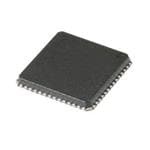
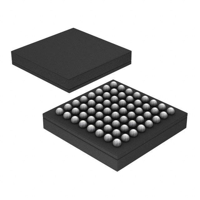
| 供应商器件封装 | 56-LFCSP-VQ(8x8) |
| 包装 | 托盘 |
| 可用A/D通道 | 10 |
| 可编程输入/输出端数量 | 34 |
| 商标 | Analog Devices |
| 处理器系列 | ADUC848 |
| 外设 | POR,PSM,PWM,温度传感器,WDT |
| 安装风格 | SMD/SMT |
| 定时器数量 | 3 Timer |
| 封装 | Tray |
| 封装/外壳 | 56-VFQFN 裸露焊盘,CSP |
| 封装/箱体 | LFCSP-56 |
| 工作温度 | -40°C ~ 85°C |
| 工厂包装数量 | 260 |
| 振荡器类型 | 内部 |
| 接口类型 | I2C/SPI/UART |
| 数据RAM大小 | 2304 B |
| 数据总线宽度 | 8 bit |
| 数据转换器 | A/D 10x16b; D/A 1x12b,2x16b |
| 最大工作温度 | + 125 C |
| 最大时钟频率 | 12 MHz |
| 最小工作温度 | - 40 C |
| 标准包装 | 1 |
| 核心 | 8052 |
| 核心处理器 | 8052 |
| 核心尺寸 | 8-位 |
| 片上ADC | Yes |
| 片上DAC | With DAC |
| 电压-电源(Vcc/Vdd) | 2.7 V ~ 3.6 V |
| 电源电压-最大 | 3.6 V, 5.25 V |
| 电源电压-最小 | 2.7 V, 4.75 V |
| 程序存储器大小 | 62 kB |
| 程序存储器类型 | Flash |
| 程序存储容量 | 8KB(8K x 8) |
| 系列 | ADUC848 |
| 输入/输出端数量 | 34 I/O |
| 连接性 | I²C, SPI, UART/USART |
| 速度 | 12.58MHz |


- 商务部:美国ITC正式对集成电路等产品启动337调查
- 曝三星4nm工艺存在良率问题 高通将骁龙8 Gen1或转产台积电
- 太阳诱电将投资9.5亿元在常州建新厂生产MLCC 预计2023年完工
- 英特尔发布欧洲新工厂建设计划 深化IDM 2.0 战略
- 台积电先进制程称霸业界 有大客户加持明年业绩稳了
- 达到5530亿美元!SIA预计今年全球半导体销售额将创下新高
- 英特尔拟将自动驾驶子公司Mobileye上市 估值或超500亿美元
- 三星加码芯片和SET,合并消费电子和移动部门,撤换高东真等 CEO
- 三星电子宣布重大人事变动 还合并消费电子和移动部门
- 海关总署:前11个月进口集成电路产品价值2.52万亿元 增长14.8%


PDF Datasheet 数据手册内容提取
MicroConverter® Multichannel 24-/16-Bit ADCs with Embedded 62 kB Flash and Single-Cycle MCU Data Sheet ADuC845/ADuC847/ADuC848 FEATURES Power Normal: 4.8 mA max at 3.6 V (core CLK = 1.57 MHz) High resolution Σ-Δ ADCs Power-down: 20 μA max with wake-up timer running 2 independent 24-bit ADCs on the ADuC845 Specified for 3 V and 5 V operation Single 24-bit ADC on the ADuC847 and Package and temperature range: single 16-bit ADC on the ADuC848 52-lead MQFP (14 mm × 14 mm), −40°C to +125°C Up to 10 ADC input channels on all devices 56-lead LFCSP (8 mm × 8 mm), −40°C to +85°C 24-bit no missing codes 22-bit rms (19.5 bit p-p) effective resolution APPLICATIONS Offset drift 10 nV/°C, gain drift 0.5 ppm/°C chop enabled Multichannel sensor monitoring Memory Industrial/environmental instrumentation 62-kbyte on-chip Flash/EE program memory Weigh scales, pressure sensors, temperature monitoring 4-kbyte on-chip Flash/EE data memory Portable instrumentation, battery-powered systems Flash/EE, 100-year retention, 100 kcycle endurance Data logging, precision system monitoring 3 levels of Flash/EE program memory security In-circuit serial download (no external hardware) High speed user download (5 sec) FUNCTIONAL BLOCK DIAGRAM 2304 bytes on-chip data RAM 8051-based core AVDD 8051-compatible instruction set ADuC845 High performance single-cycle core AVCO CURRENT IEXC1 32 kHz external crystal SOURCE IEXC2 AIN1 O3 n×- 1ch6-ipb ipt rtoimgrearm/comuanbtleer PLL (12.58 MHz max) BUF PGA 24-PBRITIMA-RYADC 1D2-ABCIT BUF DAC MUX 24 programmable I/O lines, plus 8 analog or digital input lines AINACINO1M0 AGND AUXILIARY DUA-LD 1A6-CBIT PWM0 11 interrupt sources, two priority levels 24-BIT-ADC MUX Dual data pointer, extended 11-bit stack pointer REFIN2+ SETENMSOPR DUAPLW 1M6-BIT PWM1 On-chip peripherals REFIN2– REFIN– EXTERNAL INTERNAL I1n2t-ebrint avlo pltoawgeer o-ountp ruest eDtA cCir cuit REFIN+ DEVTREEFCT BANVDRE GFAP SINGLE-CYCLE 8061-BASED MCU Dual 16-bit Σ-Δ DACs RESET 62kBYTES FLASH/EE PROGRAM MEMORY On-chip temperature sensor (ADuC845 only) DVDD POR 4kBYT2E3S0 4F LBAYSTHE/SE EU SDEART AR AMMEMORY Dual excitation current sources (200 μA) DGND PCLLL OACNKD DPIRVG 3BAU1D6 BRIATT TEIMTIEMRESR PWOWATECRH SDUOPGP LTYIM MEORN TUiAmReT ,i nStPeIr®v, aaln cdo Iu2nCt®e sre (rwiaalk Ie/O-u p/RTC timer) OSC RWTACK TEIM-UEPR/ 4P POARRTASLLEL UARSTE,SRPIAI,LA IN/ODI2C 04741-001 High speed dedicated baud rate generator (incl. 115,200) XTAL1 XTAL2 Watchdog timer (WDT) Figure 1. ADuC845 Functional Block Diagram Power supply monitor (PSM) Rev. D Document Feedback Information furnished by Analog Devices is believed to be accurate and reliable. However, no responsibility is assumed by Analog Devices for its use, nor for any infringements of patents or other One Technology Way, P.O. Box 9106, Norwood, MA 02062-9106, U.S.A. rights of third parties that may result from its use. Specifications subject to change without notice. No license is granted by implication or otherwise under any patent or patent rights of Analog Devices. Tel: 781.329.4700 ©2004–2016 Analog Devices, Inc. All rights reserved. Trademarks and registered trademarks are the property of their respective owners. Technical Support www.analog.com
ADuC845/ADuC847/ADuC848 Data Sheet TABLE OF CONTENTS Features .............................................................................................. 1 ADC Power-On .......................................................................... 36 Applications ....................................................................................... 1 Typical Performance Characteristics ........................................... 37 Revision History ............................................................................... 3 Functional Description .................................................................. 39 Specifications ..................................................................................... 4 ADC SFR Interface ..................................................................... 39 Abosolute Maximum Ratings ....................................................... 10 ADCSTAT (ADC Status Register) ........................................... 40 ESD Caution ................................................................................ 10 ADCMODE (ADC Mode Register) ......................................... 41 Pin Configurations and Function Descriptions ......................... 11 ADC0CON1 (Primary ADC Control Register) ..................... 43 General Description ....................................................................... 15 ADC0CON2 (Primary ADC Channel Select Register) ........ 44 8052 Instruction Set ................................................................... 18 SF (ADC Sinc Filter Control Register) .................................... 46 Timer Operation ......................................................................... 18 ICON (Excitation Current Sources Control Register) .......... 47 ALE ............................................................................................... 18 Nonvolatile Flash/EE Memory Overview ............................... 48 External Memory Access ........................................................... 18 Flash/EE Program Memory ...................................................... 49 Complete SFR Map .................................................................... 19 User Download Mode (ULOAD) ............................................. 50 Functional Description .................................................................. 20 Using Flash/EE Data Memory .................................................. 51 8051 Instruction Set ................................................................... 20 Flash/EE Memory Timing ........................................................ 52 Memory Organization ............................................................... 22 DAC Circuit Information .......................................................... 53 Special Function Registers (SFRs) ............................................ 24 Pulse-Width Modulator (PWM) .............................................. 55 ADC Circuit Information .......................................................... 26 On-Chip PLL (PLLCON) .......................................................... 60 Auxiliary ADC (ADuC845 Only) ............................................ 32 I2C Serial Interface ..................................................................... 61 Reference Inputs ......................................................................... 32 SPI Serial Interface ..................................................................... 63 Burnout Current Sources .......................................................... 32 Using the SPI Interface .............................................................. 66 Reference Detect Circuit ........................................................... 33 Dual Data Pointers ..................................................................... 67 Sinc Filter Register (SF) ............................................................. 33 Power Supply Monitor ............................................................... 68 Σ-Δ Modulator ............................................................................ 33 Watchdog Timer ......................................................................... 69 Digital Filter ................................................................................ 33 Time Interval Counter (TIC) .................................................... 70 ADC Chopping ........................................................................... 34 8052-Compatible On-Chip Peripherals .................................. 73 Calibration ................................................................................... 34 Timers/Counters ........................................................................ 75 Programmable Gain Amplifier ................................................. 35 UART Serial Interface ................................................................ 80 Bipolar/Unipolar Configuration .............................................. 35 Interrupt System ......................................................................... 87 Data Output Coding .................................................................. 36 Interrupt Priority ........................................................................ 88 Excitation Currents .................................................................... 36 Interrupt Vectors ........................................................................ 88 Rev. D | Page 2 of 110
Data Sheet ADuC845/ADuC847/ADuC848 Hardware Design Considerations ................................................. 89 Other Hardware Considerations ............................................... 92 External Memory Interface ........................................................ 89 QuickStart Development System .................................................. 96 Power Supplies ............................................................................. 89 QuickStart-PLUS Development System .................................. 96 Power-On Reset Operation ........................................................ 90 Timing Specifications ..................................................................... 97 Power Consumption ................................................................... 90 Outline Dimensions ...................................................................... 106 Power-Saving Modes .................................................................. 90 Ordering Guide ......................................................................... 107 Grounding and Board Layout Recommendations ................. 91 REVISION HISTORY 5/2016—Rev. C to Rev. D 6/2004—Rev. 0 to Rev. A Changed uC004 to AN-1074 ....................................... Throughout Changes to Figure 5 ........................................................................ 17 Updated Outline Dimensions ......................................................108 Changes to Figure 6 ........................................................................ 18 Changes to Ordering Guide .........................................................109 Changes to Figure 7 ........................................................................ 19 Changes to Table 5 .......................................................................... 24 12/2012—Rev. B to Rev. C Changes to Table 24 ........................................................................ 41 Changes to Figure 3 and Table 3 ................................................... 11 Changes to Table 25 ........................................................................ 43 Changes to Burnout Current Sources Section ............................. 32 Changes to Table 26 ........................................................................ 44 Change to ADCMODE (ADC Mode Register) Section............. 42 Changes to Table 27 ........................................................................ 45 Changes to Mode 4 (Dual NRZ 16-Bit Σ-Δ DAC) Section ............ 58 Changes to User Download Mode Section .................................. 50 Change to Hardware Slave Mode Section .................................... 63 Added Figure 51 and Renumbered Subsequent Figures ............ 50 Updated Outline Dimensions ......................................................104 Edits to the DACH/DACL Data Registers Section ..................... 53 Changes to Ordering Guide .........................................................105 Changes to Table 34 ........................................................................ 56 Added SPIDAT: SPI Data Register Section ................................. 65 2/2005—Rev. A to Rev. B Changes to Table 42 ........................................................................ 67 Changes to Figure 1 ........................................................................... 1 Changes to Table 43 ........................................................................ 68 Changes to the Burnout Current Sources Section ...................... 32 Changes to Table 44 ........................................................................ 69 Changes to the Excitation Currents Section ................................ 36 Changes to Table 45 ........................................................................ 71 Changes to Table 30 ........................................................................ 47 Changes to Table 50 ........................................................................ 75 Changes to the Flash/EE Memory on the ADuC845, ADuC847, Changes to Timer/Counter 0 and 1 Data Registers Section ........... 76 ADuC848 Section ............................................................................. 48 Changes to Table 54 ........................................................................ 80 Changes to Figure 39 ...................................................................... 57 Added the SBUF—UART Serial Port Data Register Section ......... 80 Changes to On-Chip PLL (PLLCON) Section ............................ 60 Addition to the Timer 3 Generated Baud Rates Section ........... 83 Added 3 V Part Section Heading .................................................. 88 Added Table 57 and Renumbered Subsequent Tables ............... 84 Added 5 V Part Section .................................................................. 88 Changes to Table 61 ........................................................................ 86 Changes to Figure 70 ...................................................................... 91 Changes to Figure 71 ...................................................................... 93 4/2004—Revision 0: Initial Version Rev. D | Page 3 of 110
ADuC845/ADuC847/ADuC848 Data Sheet SPECIFICATIONS1 AV = 2.7 V to 3.6 V or 4.75 V to 5.25 V, DV = 2.7 V to 3.6 V or 4.75 V to 5.25 V, REFIN(+) = 2.5 V, REFIN(–) = AGND; AGND = DD DD DGND = 0 V; XTAL1/XTAL2 = 32.768 kHz crystal; all specifications T to T , unless otherwise noted. Input buffer on for primary MIN MAX ADC, unless otherwise noted. Core speed = 1.57 MHz (default CD = 3), unless otherwise noted. Table 1. Parameter Min Typ Max Unit Test Conditions/Comments PRIMARY ADC Conversion Rate 5.4 105 Hz Chop on (ADCMODE.3 = 0) 16.06 1365 Hz Chop off (ADCMODE.3 = 1) No Missing Codes2 24 Bits ≤26.7 Hz update rate with chop enabled 24 Bits ≤80.3 Hz update rate with chop disabled Resolution (ADuC845/ADuC847) See Table 11 and Table 15 Resolution (ADuC848) See Table 13 and Table 17 Output Noise (ADuC845/ADuC847) See Table 10 and Table 14 μV (rms) Output noise varies with selected update rates, gain range, and chop status. Output Noise (ADuC848) See Table 12 and Table 16 μV (rms) Output noise varies with selected update rates, gain range, and chop status. Integral Nonlinearity ±15 ppm of FSR 1 LSB 16 Offset Error3 ±3 μV Chop on Chop off, offset error is in the order of the noise for the programmed gain and update rate following a calibration. Offset Error Drift vs. Temperature2 ±10 nV/°C Chop on (ADCMODE.3 = 0) ±200 nV/°C Chop off (ADCMODE.3 = 1) Full-Scale Error4 ADuC845/ADuC847 ±10 μV ±20 mV to ±2.56 V ADuC848 ±10 μV ±20 mV to ±640 mV ±0.5 LSB ±1.28 V to ±2.56 V 16 Gain Error Drift vs. Temperature4 ±0.5 ppm/°C Power Supply Rejection 80 dB AIN = 1 V, ±2.56 V, chop enabled 113 dB AIN = 7.8 mV, ±20 mV, chop enabled 80 dB AIN = 1 V, ±2.56 V, chop disabled2 PRIMARY ADC ANALOG INPUTS Differential Input Voltage Ranges 5, 6 Gain = 1 to 128 Bipolar Mode (ADC0CON1.5 = 0) ±1.024 × V V = REFIN(+) − REFIN(−) or REFIN2(+) − REF V /GAIN REFIN2(−) (or Int 1.25 V ) REF REF Unipolar Mode (ADC0CON1.5 = 1) 0 – 1.024 × V V = REFIN(+) − REFIN(−) or REFIN2(+) − REF V /GAIN REFIN2(−) (or Int 1.25 V ) REF REF ADC Range Matching ±2 μV AIN = 18 mV, chop enabled Common-Mode Rejection DC Chop enabled, chop disabled On AIN 95 dB AIN = 7.8 mV, range = ±20 mV 113 dB AIN = 1 V, range = ±2.56 V Common-Mode Rejection 50 Hz/60 Hz ± 1 Hz, 16.6 Hz and 50 Hz update 50 Hz/60 Hz2 rate, chop enabled, REJ60 enabled On AIN 95 dB AIN = 7.8 mV, range = ±20 mV 90 dB AIN = 1 V, range = ±2.56 V Rev. D | Page 4 of 110
Data Sheet ADuC845/ADuC847/ADuC848 Parameter Min Typ Max Unit Test Conditions/Comments Normal Mode Rejection 50 Hz/60 Hz2 On AIN 75 dB 50 Hz/60 Hz ± 1 Hz, 16.6 Hz Fadc, SF = 52H, chop on, REJ60 on 100 dB 50 Hz ± 1 Hz, 16.6 Hz Fadc, SF = 52H, chop on 67 dB 50 Hz/60 Hz ± 1 Hz, 50 Hz Fadc, SF = 52H, chop off, REJ60 on 100 dB 50 Hz ± 1 Hz, 50 Hz Fadc, SF = 52H, chop off Analog Input Current2 ±1 nA T = 85°C, buffer on MAX ±5 nA T = 125°C, buffer on MAX Analog Input Current Drift ±5 pA/°C T = 85°C, buffer on MAX ±15 pA/°C T = 125°C, buffer on MAX Average Input Current ±125 nA/V ±2.56 V range, buffer bypassed Average Input Current Drift ±2 pA/V/°C Buffer bypassed Absolute AIN Voltage Limits2 A + AV − V AIN1 … AIN10 and AINCOM with buffer enabled GND DD 0.1 0.1 Absolute AIN Voltage Limits2 A − AV + V AIN1 … AIN10 and AINCOM with buffer bypassed GND DD 0.03 0.03 EXTERNAL REFERENCE INPUTS REFIN(+) to REFIN(–) Voltage 2.5 V REFIN refers to both REFIN and REFIN2 REFIN(+) to REFIN(–) Range2 1 AV V REFIN refers to both REFIN and REFIN2 DD Average Reference Input Current ±1 μA/V Both ADCs enabled Average Reference Input Current ±0.1 nA/V/°C Drift NOXREF Trigger Voltage 0.3 0.65 V NOXREF (ADCSTAT.4) bit active if V > 0.3 V, and REF inactive if V > 0.65 V REF Common-Mode Rejection DC Rejection 125 dB AIN = 1 V, range = ±2.56 V 50 Hz/60 Hz Rejection2 90 dB 50 Hz/60 Hz ± 1 Hz, AIN = 1 V, range = ±2.56 V, SF = 82 Normal Mode Rejection 75 dB 50 Hz/60 Hz ±1 Hz, AIN = 1 V, range = ±2.56 V, 50 Hz/60 Hz2 SF = 52H, chop on, REJ60 on 100 dB 50 Hz ± 1 Hz, AIN = 1 V, range = ±2.56 V, SF = 52H, chop on 67 dB 50 Hz/60 Hz ± 1 Hz, AIN = 1 V, range = ±2.56 V, SF = 52H, chop off, REJ60 on 100 dB 50 Hz ± 1 Hz, AIN = 1 V, range = ±2.56 V, SF = 52H, chop off AUXILIARY ADC (ADuC845 Only) Conversion Rate 5.4 105 Hz Chop on 16.06 1365 Hz Chop off No Missing Codes2 24 Bits ≤26.7 Hz update rate, chop enabled 24 Bits 80.3 Hz update rate, chop disabled Resolution See Table 19 and Table 21 Output Noise See Table 18 and Table 20 Output noise varies with selected update rates. Integral Nonlinearity ±15 ppm of FSR 1 LSB 16 Offset Error3 ±3 μV Chop on ±0.25 LSB Chop off 16 Offset Error Drift2 10 nV/°C Chop on 200 nV/°C Chop off Full-Scale Error4 ±0.5 LSB 16 Gain Error Drift4 ±0.5 ppm/°C Power Supply Rejection 80 dB AIN = 1 V, range = ±2.56 V, chop enabled 80 dB AIN = 1 V, range = ±2.56 V, chop disabled Rev. D | Page 5 of 110
ADuC845/ADuC847/ADuC848 Data Sheet Parameter Min Typ Max Unit Test Conditions/Comments AUXILIARY ADC ANALOG INPUTS (ADuC845 ONLY) Differential Input Voltage Ranges5, 6 Bipolar Mode (ADC1CON.5 = 0) ±V V REFIN = REFIN(+) − REFIN(−) (or Int 1.25 V ) REF REF Unipolar Mode (ADC1CON.5 = 1) 0 – V V REFIN = REFIN(+) − REFIN(−) (or Int 1.25 V ) REF REF Average Analog Input Current 125 nA/V Analog Input Current Drift ±2 pA/V/°C Absolute AIN/AINCOM Voltage A − AV + V GND DD Limits2, 7 0.03 0.03 Normal Mode Rejection 50 Hz/60 Hz2 On AIN and REFIN 75 dB 50 Hz/60 Hz ± 1 Hz, 16.6 Hz Fadc, SF = 52H, chop on, REJ60 on 100 dB 50 Hz ± 1 Hz, 16.6 Hz Fadc, SF = 52H, chop on 67 dB 50 Hz/60 Hz ± 1 Hz, 50 Hz Fadc, SF = 52H, chop off, REJ60 on 100 dB 50 Hz ± 1 Hz, 50 Hz Fadc, SF = 52H, chop off ADC SYSTEM CALIBRATION Full-Scale Calibration Limit +1.05 × FS V Zero-Scale Calibration Limit −1.05 × FS V Input Span 0.8 × FS 2.1 × FS V DAC Voltage Range 0 – V V DACCON.2 = 0 REF 0 – AV V DACCON.2 = 1 DD Resistive Load 10 kΩ From DAC output to AGND Capactive Load 100 pF From DAC output to AGND Output Impedance 0.5 Ω I 50 μA SINK DC Specifications8 Resolution 12 Bits Relative Accuracy ±3 LSB Differential Nonlinearity −1 LSB Guaranteed 12-bit monotonic Offset Error ±50 mV Gain Error ±1 % AV range DD ±1 % V range REF AC Specifications2, 8 Voltage Output Settling Time 15 μs Settling time to 1 LSB of final value Digital-to-Analog Glitch Energy 10 nVs 1 LSB change at major carry INTERNAL REFERENCE ADC Reference Chop enabled Reference Voltage 1.25 − 1% 1.25 1.25 + 1% V Initial tolerance @ 25°C, V = 5 V DD Power Supply Rejection 45 dB Reference Tempco 100 ppm/°C DAC Reference Reference Voltage 2.5 – 1% 2.5 2.5 + 1% ±1% V Initial tolerance @ 25°C, V = 5 V DD Power Supply Rejection 50 dB Reference Tempco ±100 ppm/°C TEMPERATURE SENSOR (ADuC845 ONLY) Accuracy ±2 °C Thermal Impedance 90 °C/W MQFP 52 °C/W LFCSP Rev. D | Page 6 of 110
Data Sheet ADuC845/ADuC847/ADuC848 Parameter Min Typ Max Unit Test Conditions/Comments TRANSDUCER BURNOUT CURRENT SOURCES AIN+ Current −100 nA AIN+ is the selected positive input (AIN4 or AIN6 only) to the primary ADC AIN− Current 100 nA AIN− is the selected negative input (AIN5 or AIN7 only) to the primary ADC Initial Tolerance at 25°C ±10 % Drift 0.03 %/°C EXCITATION CURRENT SOURCES Output Current 200 μA Available from each current source Initial Tolerance at 25°C ±10 % Drift 200 ppm/°C Initial Current Matching at 25°C ±1 % Matching between both current sources Drift Matching 20 ppm/°C Line Regulation (AV ) 1 μA/V AV = 5 V ± 5% DD DD Load Regulation 0.1 μA/V Output Compliance2 AGND AV − 0.6 V DD POWER SUPPLY MONITOR (PSM) AV Trip Point Selection Range 2.63 4.63 V Four trip points selectable in this range DD AV Trip Point Accuracy ±3.0 % T = 85°C DD MAX ±4.0 % T = 125°C MAX DV Trip Point Selection Range 2.63 4.63 V Four trip points selectable in this range DD DV Trip Point Accuracy ±3.0 % T = 85°C DD MAX ±4.0 % T = 125°C MAX CRYSTAL OSCILLATOR (XTAL1 AND XTAL2) Logic Inputs, XTAL1 Only2 V , Input Low Voltage 0.8 V DV = 5 V INL DD 0.4 V DV = 3 V DD V , Input Low Voltage 3.5 V DV = 5 V INH DD 2.5 V DV = 3 V DD XTAL1 Input Capacitance 18 pF XTAL2 Output Capacitance 18 pF LOGIC INPUTS All Inputs Except SCLOCK, RESET, and XTAL12 V , Input Low Voltage 0.8 V DV = 5 V INL DD 0.4 V DV = 3 V DD V , Input Low Voltage 2.0 V INH SCLOCK and RESET Only (Schmidt Triggered Inputs)2 V 1.3 3.0 V DV = 5 V T+ DD 0.95 2.5 V DV = 3 V DD V 0.8 1.4 V DV = 5 V T− DD 0.4 1.1 V DV = 3 V DD V − V 0.3 0.85 V DV = 5 V or 3 V T+ T− DD Input Currents Port 0, P1.0 to P1.7, EA ±10 μA V = 0 V or V IN DD RESET ±10 μA V = 0 V, DV = 5 V IN DD 35 105 μA V = DV , DV = 5 V, internal pull-down IN DD DD Port 2, Port 3 ±10 μA V = DV , DV = 5 V IN DD DD −180 −660 μA V = 2 V, DV = 5 V IN DD −20 −75 μA V = 0.45 V, DV = 5 V IN DD Input Capacitance 10 pF All digital inputs Rev. D | Page 7 of 110
ADuC845/ADuC847/ADuC848 Data Sheet Parameter Min Typ Max Unit Test Conditions/Comments LOGIC OUTPUTS (ALL DIGITAL OUTPUTS EXCEPT XTAL2) V , Output High Voltage2 2.4 V DV = 5 V, I = 80 μA OH DD SOURCE 2.4 V DV = 3 V, I = 20 μA DD SOURCE V , Output Low Voltage 0.4 V I = 8 mA, SCLOCK, SDATA OL SINK 0.4 V I = 1.6 mA on P0, P1, P2 SINK Floating State Leakage Current2 ±10 μA Floating State Output Capacitance 10 pF START-UP TIME At Power-On 600 ms After Ext RESET in Normal Mode 3 ms After WDT RESET in Normal Mode 2 ms Controlled via WDCON SFR From Power-Down Mode Oscillator Running PLLCON.7 = 0 Wake-Up with INT0 Interrupt 20 μs Wake-Up with SPI Interrupt 20 μs Wake-Up with TIC Interrupt 20 μs Oscillator Powered Down PLLCON.7 = 1 Wake-Up with INT0 Interrupt 30 μs Wake-Up with SPI Interrupt 30 μs FLASH/EE MEMORY RELIABILITY CHARACTERISTICS Endurance9 100,000 Cycles Data Retention10 100 Years POWER REQUIREMENTS Power Supply Voltages AV 3 V Nominal 2.7 3.6 V DD AV 5 V Nominal 4.75 5.25 V DD DV 3 V Nominal 2.7 3.6 V DD DV 5 V Nominal 4.75 5.25 V DD 5 V Power Consumption 4.75 V < DV < 5.25 V, AV = 5.25 V DD DD Normal Mode11, 12 DV Current 10 mA Core clock = 1.57 MHz DD 25 31 mA Core clock = 12.58 MHz AV Current 180 μA DD Power-Down Mode11, 12 DV Current 40 53 μA T = 85°C; OSC on; TIC on DD MAX 50 μA T = 125°C; OSC on; TIC on MAX 20 33 μA T = 85°C; OSC off MAX 30 μA T = 125°C; OSC off MAX AV Current 1 μA T = 85°C; OSC on or off DD MAX 3 μA T = 125°C; OSC on or off MAX Typical Additional Peripheral 5 V V , CD = 3 DD Currents (AI and DI ) DD DD Primary ADC 1 mA Auxiliary ADC (ADuC845 Only) 0.5 mA Power Supply Monitor 30 μA DAC 60 μA DACH/L = 000H Dual Excitation Current Sources 200 μA 200 μA each. Can be combined to give 400 μA on a single output. ALE Off −20 μA PCON.4 = 1 (see Table 6) WDT 10 μA Rev. D | Page 8 of 110
Data Sheet ADuC845/ADuC847/ADuC848 Parameter Min Typ Max Unit Test Conditions/Comments PWM −Fxtal 3 μA −Fvco 0.5 mA TIC 1 μA 3 V Power Consumption 2.7 V < DV < 3.6 V, AV = 3.6 V DD DD Normal Mode11, 12 DV Current 4.8 mA Core clock = 1.57 MHz DD 9 11 mA Core clock = 6.29 MHz (CD = 1) AV Current 180 μA ADC not enabled DD Power-Down Mode11, 12 DV Current 20 26 μA T = 85°C; OSC on; TIC on DD MAX 29 μA T = 125°C; OSC on; TIC on MAX 14 20 μA T = 85°C; OSC off MAX 21 μA T = 125°C; OSC off MAX AV Current 1 μA T = 85°C; OSC on or off DD MAX 3 μA T = 125°C; OSC on or off MAX 1 Temperature range is for ADuC845BS; for the ADuC847BS and ADuC848BS (MQFP package), the range is –40°C to +125°C. Temperature range for ADuC845BCP, ADuC847BCP, and ADuC848BCP (LFCSP package) is –40°C to +85°C. 2 These numbers are not production tested but are guaranteed by design and/or characterization data on production release. 3 System zero-scale calibration can remove this error. 4 Gain error drift is a span drift. To calculate full-scale error drift, add the offset error drift to the gain error drift times the full-scale input. 5 In general terms, the bipolar input voltage range to the primary ADC is given by the ADC range = ±(VREF 2RN )/1.25, where: VREF = REFIN(+) to REFIN(–) voltage and VREF = 1.25 V when internal ADC VREF is selected. RN = decimal equivalent of RN2, RN1, RN0. For example, if VREF = 2.5 V and RN2, RN1, RN0 = 1, 1, 0, respectively, then the ADC range = ±1.28 V. In unipolar mode, the effective range is 0 V to 1.28 V in this example. 6 1.25 V is used as the reference voltage to the ADC when internal VREF is selected via XREF0/XREF1 or AXREF bits in ADC0CON2 and ADC1CON, respectively. (AXREF is available only on the ADuC845.) 7 In bipolar mode, the auxiliary ADC can be driven only to a minimum of AGND – 30 mV as indicated by the auxiliary ADC absolute AIN voltage limits. The bipolar range is still –VREF to +VREF. 8 DAC linearity and ac specifications are calculated using a reduced code range of 48 to 4095, 0 V to VREF, reduced code range of 100 to 3950, 0 V to VDD. 9 Endurance is qualified to 100 kcycle per JEDEC Std. 22 method A117 and measured at –40°C, +25°C, +85°C, and +125°C. Typical endurance at 25°C is 700 kcycles. 10 Retention lifetime equivalent at junction temperature (TJ) = 55°C per JEDEC Std. 22, Method A117. Retention lifetime based on an activation energy of 0.6 eV derates with junction temperature. 11 Power supply current consumption is measured in normal mode following the power-on sequence, and in power-down modes under the following conditions: Normal mode: reset = 0.4 V, digital I/O pins = open circuit, Core Clk changed via CD bits in PLLCON, core executing internal software loop. Power-down mode: reset = 0.4 V, all P0 pins and P1.2 to P1.7 pins = 0.4 V. All other digital I/O pins are open circuit, core Clk changed via CD bits in PLLCON, PCON.1 = 1, core execution suspended in power-down mode, OSC turned on or off via OSC_PD bit (PLLCON.7) in PLLCON SFR. 12 DVDD power supply current increases typically by 3 mA (3 V operation) and 10 mA (5 V operation) during a Flash/EE memory program or erase cycle. General Notes about Specifications DAC gain error is a measure of the span error of the DAC. The ADuC845BCP, ADuC847BCP, and ADuC848BCP (LFCSP package) have been qualified and tested with the base of the LFCSP package floating. The base of the LFCSP package should be soldered to the board, but left floating electrically, to ensure good mechanical stability. Flash/EE memory reliability characteristics apply to both the Flash/EE program memory and Flash/EE data memory. Rev. D | Page 9 of 110
ADuC845/ADuC847/ADuC848 Data Sheet ABOSOLUTE MAXIMUM RATINGS T = 25°C, unless otherwise noted. Stresses at or above those listed under Absolute Maximum A Ratings may cause permanent damage to the product. This is a Table 2. stress rating only; functional operation of the product at these Parameter Rating or any other conditions above those indicated in the operational AV to AGND –0.3 V to +7 V section of this specification is not implied. Operation beyond DD AV to DGND –0.3 V to +7 V the maximum operating conditions for extended periods may DD DV to DGND –0.3 V to +7 V affect product reliability. DD DV to DGND –0.3 V to +7 V DD AGND to DGND1 –0.3 V to +0.3 V AVDD to DVDD –2 V to +5 V ESD CAUTION Analog Input Voltage to AGND2 –0.3 V to AV + 0.3 V DD Reference Input Voltage to AGND –0.3 V to AV + 0.3 V DD AIN/REFIN Current (Indefinite) 30 mA Digital Input Voltage to DGND –0.3 V to DV + 0.3 V DD Digital Output Voltage to DGND –0.3 V to DV + 0.3 V DD Operating Temperature Range –40°C to +125°C Storage Temperature Range –65°C to +150°C Junction Temperature 150°C θ Thermal Impedance (MQFP) 90°C/W JA θ Thermal Impedance (LFCSP) 52°C/W JA Lead Temperature, Soldering Vapor Phase (60 sec) 215°C Infrared (15 sec) 220°C 1 AGND and DGND are shorted internally on the ADuC845, ADuC847, and ADuC848. 2 Applies to the P1.0 to P1.7 pins operating in analog or digital input modes. Rev. D | Page 10 of 110
Data Sheet ADuC845/ADuC847/ADuC848 PIN CONFIGURATIONS AND FUNCTION DESCRIPTIONS P0.7/AD7P0.6/AD6P0.5/AD5P0.4/AD4DVDDDGNDP0.3/AD3P0.2/AD2P0.1/AD1P0.0/AD0ALE PSENEA P1.0/AIN1P0.7/AD7 P0.6/AD6P0.5/AD5 P0.4/AD4DVDDDGNDP0.3/AD3 P0.2/AD2P0.1/AD1P0.0/AD0 ALE PSENEA 52 51 5049 48 4746 45 4443 42 41 40 P1.0/AIN1 1 PIN 1 39 P2.7/PWMCLK P1.1/AIN2 15655545352515049 484746 45444342 P2.7/PWMCLK P1.1/AIN2 2 IDENTIFIER 38 P2.6/PWM1 P1.2/AIN3/REFIN2+ 2 41 P2.6/PWM1 P1.2/AIN3/REFIN2+ 3 37 P2.5/PWM0 P1.3/AIN4/REFIN2– 3 40 P2.5/PWM0 P1.3/AIN4/REFIN2– 4 36 P2.4/T2EX AVDD 4 39 P2.4/T2EX REAAFGVINNDDD– 567 ADuC845/ADuC847/ADuC848 333543 DXDGVTADNDLD2 RAAEGFGINNNDD– 567 ADuCA8D45u/CA8D4u8C847/ 333876 DDDGGVNDNDDD PR1.E4/FAIINN+5 89 (NToOtPtoVSIEcaWle) 3321 PX2T.A3/LS1S/T2 P1R.4E/AFIINN+5 89 (NToOt Pto V SIEcaWle) 3354 XXTTAALL21 P1.5/AIN6 10 30 P2.2/MISO P1.5/AIN6 10 33 P2.3/SS/T2 P1.6/AIN7/IEXC1 11 29 P2.1/MOSI P1.6/AIN7/IEXC1 11 32 P2.2/MISO P1.7/AIN8/IEXC2 12 31 P2.1/MOSI P1.7/AIN8/IEXC2 12 28 P2.0/SCLOCK (SPI) AINCOM/DAC 13 30 P2.0/SCLOCK (SPI) AINCOM/DAC 13 27 SDATA DAC 14 29 SDATA 14 15 16 17 18 19 20 21 22 23 24 25 26 1516171819202122232425262728 FiguDACre RESET2. 5P3.0/RxD2-P3.1/TxDLeaP3.2/INT0d P3.3/INT1MQDVDDFPDGND PP3.4/T0in CP3.5/T1onP3.6/WRfigP3.7/RDur2SCLOCK (IC)ation 04741-002 N1.O TTHEES EAIN9XPAIN10OSRESETED P3.0/RxDPADP3.1/TxDDLP3.2/INT0E MP3.3/INT1USDVDDT BDGNDE LP3.4/T0EFP3.5/T1T UP3.6/WRNCP3.7/RDON2SCLK (IC)NECTED. 04741-003 Figure 3. 56-Lead LFCSP Pin Configuration Table 3. Pin Function Descriptions Pin No. 52-MQFP 56-LFCSP Mnemonic Type1 Description 1 56 P1.0/AIN1 I By power-on default, P1.0/AIN1 is configured as the AIN1 analog input. AIN1 can be used as a pseudo differential input when used with AINCOM or as the positive input of a fully differential pair when used with AIN2. P1.0 has no digital output driver. It can function as a digital input for which 0 must be written to the port bit. As a digital input, this pin must be driven high or low externally. 2 1 P1.1/AIN2 I On power-on default, P1.1/AIN2 is configured as the AIN2 analog input. AIN2 can be used as a pseudo differential input when used with AINCOM or as the negative input of a fully differential pair when used with AIN1. P1.1 has no digital output driver. It can function as a digital input for which 0 must be written to the port bit. As a digital input, this pin must be driven high or low externally. 3 2 P1.2/AIN3/REFIN2+ I On power-on default, P1.2/AIN3 is configured as the AIN3 analog input. AIN3 can be used as a pseudo differential input when used with AINCOM or as the positive input of a fully differential pair when used with AIN4. P1.2 has no digital output driver. It can function as a digital input for which 0 must be written to the port bit. As a digital input, this pin must be driven high or low externally. This pin also functions as a second external differential reference input, positive terminal. 4 3 P1.3/AIN4/REFIN2− I On power-on default, P1.3/AIN4 is configured as the AIN4 analog input. AIN4 can be used as a pseudo differential input when used with AINCOM or as the negative input of a fully differential pair when used with AIN3. P1.3 has no digital output driver. It can function as a digital input for which 0 must be written to the port bit. As a digital input, this pin must be driven high or low externally. This pin also functions as a second external differential reference input, negative terminal. 5 4 AV S Analog Supply Voltage. DD 6 5 AGND S Analog Ground. Not 6 AGND S A second analog ground is provided with the LFCSP version only. applicable 7 7 REFIN− I External Differential Reference Input, Negative Terminal. 8 8 REFIN+ I External Differential Reference Input, Positive Terminal. Rev. D | Page 11 of 110
ADuC845/ADuC847/ADuC848 Data Sheet Pin No. 52-MQFP 56-LFCSP Mnemonic Type1 Description 9 9 P1.4/AIN5 I On power-on default, P1.4/AIN5 is configured as the AIN5 analog input. AIN5 can be used as a pseudo differential input when used with AINCOM or as the positive input of a fully differential pair when used with AIN6. P1.0 has no digital output driver. It can function as a digital input for which 0 must be written to the port bit. As a digital input, this pin must be driven high or low externally. 10 10 P1.5/AIN6 I On power-on default, P1.5/AIN6 is configured as the AIN6 analog input. AIN6 can be used as a pseudo differential input when used with AINCOM or as the negative input of a fully differential pair when used with AIN5. P1.1 has no digital output driver. It can function as a digital input for which 0 must be written to the port bit. As a digital input, this pin must be driven high or low externally. 11 11 P1.6/AIN7/IEXC1 I/O On power-on default, P1.6/AIN7 is configured as the AIN7 analog input. AIN7 can be used as a pseudo differential input when used with AINCOM or as the positive input of a fully differential pair when used with AIN8. One or both current sources can also be configured at this pin. P1.6 has no digital output driver. It can, however, function as a digital input for which 0 must be written to the port bit. As a digital input, this pin must be driven high or low externally. 12 12 P1.7/AIN8/IEXC2 I/O On power-on default, P1.7/AIN8 is configured as the AIN8 analog input. AIN8 can be used as a pseudo differential input when used with AINCOM or as the negative input of a fully differential pair when used with AIN7. One or both current sources can also be configured at this pin. P1.7 has no digital output driver. It can, however, function as a digital input for which 0 must be written to the port bit. As a digital input, this pin must be driven high or low externally. 13 13 AINCOM/DAC I/O All analog inputs can be referred to this pin, provided that a relevant pseudo differential input mode is selected. This pin also functions as an alternative pin out for the DAC. 14 14 DAC O The voltage output from the DAC, if enabled, appears at this pin. Not 15 AIN9 I AIN9 can be used as a pseudo differential analog input when used with applicable AINCOM or as the positive input of a fully differential pair when used with AIN10 (LFCSP version only). Not 16 AIN10 I AIN10 can be used as a pseudo differential analog input when used with applicable AINCOM or as the negative input of a fully differential pair when used with AIN9 (LFCSP version only). 15 17 RESET I Reset Input. A high level on this pin for 16 core clock cycles while the oscillator is running resets the device. This pin has an internal weak pull-down and a Schmitt trigger input stage. 16 to 19, 18 to 21, P3.0 to P3.7 I/O P3.0 to P3.7 are bidirectional port pins with internal pull-up resistors. Port 3 22 to 25 24 to 27 pins that have 1s written to them are pulled high by the internal pull-up resistors, and in that state can be used as inputs. As inputs, Port 3 pins being pulled externally low source current because of the internal pull-up resistors. When driving a 0-to-1 output transition, a strong pull-up is active for one core clock period of the instruction cycle. Port 3 pins also have the various secondary functions described in this table. 16 18 P3.0/RxD Receiver Data for UART Serial Port. 17 19 P3.1/TxD Transmitter Data for UART Serial Port. 18 20 P3.2/INT0 External Interrupt 0. This pin can also be used as a gate control input to Timer 0. 19 21 P3.3/INT1 External Interrupt 1. This pin can also be used as a gate control input to Timer 1. 22 24 P3.4/T0 Timer/Counter 0 External Input. 23 25 P3.5/T1 Timer/Counter 1 External Input. 24 26 P3.6/WR External Data Memory Write Strobe. This pin latches the data byte from Port 0 into an external data memory. 25 27 P3.7/RD External Data Memory Read Strobe. This pin enables the data from an external data memory to Port 0. Rev. D | Page 12 of 110
Data Sheet ADuC845/ADuC847/ADuC848 Pin No. 52-MQFP 56-LFCSP Mnemonic Type1 Description 20, 34, 48 22, 36, 51 DV S Digital Supply Voltage. DD 21, 35, 47 23, 37, 38, DGND S Digital Ground. 50 26 28 SCLK (I2C) I/O Serial Interface Clock for the I2C Interface. As an input, this pin is a Schmitt- triggered input. A weak internal pull-up is present on this pin unless it is outputting logic low. This pin can also be controlled in software as a digital output pin. 27 29 SDATA I/O Serial Data Pin for the I2C Interface. As an input, this pin has a weak internal pull-up present unless it is outputting logic low. 28 to 31, 30 to 33, P2.0 to P2.7 I/O Port 2 is a bidirectional port with internal pull-up resistors. Port 2 pins that 36 to 39 39 to 42 have 1s written to them are pulled high by the internal pull-up resistors, and in that state can be used as inputs. As inputs, Port 2 pins being pulled externally low source current because of the internal pull-up resistors. Port 2 emits the middle and high-order address bytes during accesses to the 24-bit external data memory space. Port 2 pins also have the various secondary functions described in this table. 28 30 P2.0/SCLOCK (SPI) Serial Interface Clock for the SPI Interface. As an input this pin is a Schmitt- triggered input. A weak internal pull-up is present on this pin unless it is outputting logic low. 29 31 P2.1/MOSI Serial Master Output/Slave Input Data for the SPI Interface. A strong internal pull-up is present on this pin when the SPI interface outputs a logic high. A strong internal pull-down is present on this pin when the SPI interface outputs a logic low. 30 32 P2.2/MISO Master Input/Slave Output for the SPI Interface. A weak pull-up is present on this input pin. 31 33 P2.3/SS/T2 Slave Select Input for the SPI Interface. A weak pull-up is present on this pin. For both package options, this pin can also be used to provide a clock input to Timer 2. When enabled, Counter 2 is incremented in response to a negative transition on the T2 input pin. 36 39 P2.4/T2EX Control Input to Timer 2. When enabled, a negative transition on the T2EX input pin causes a Timer 2 capture or reload event. 37 40 P2.5/PWM0 If the PWM is enabled, the PWM0 output appears at this pin. 38 41 P2.6/PWM1 If the PWM is enabled, the PWM1 output appears at this pin. 39 42 P2.7/PWMCLK If the PWM is enabled, an external PWM clock can be provided at this pin. 32 34 XTAL1 I Input to the Crystal Oscillator Inverter. 33 35 XTAL2 O Output from the Crystal Oscillator Inverter. See the Hardware Design Considerations section for a description. 40 43 EA External Access Enable, Logic Input. When held high, this input enables the device to fetch code from internal program memory locations 0000H to F7FFH. No external program memory access is available on the ADuC845, ADuC847, or ADuC848. To determine the mode of code execution, the EA pin is sampled at the end of an external RESET assertion or as part of a device power cycle. EA can also be used as an external emulation I/O pin, and therefore the voltage level at this pin must not be changed during normal operation because this might cause an emulation interrupt that halts code execution. 41 44 PSEN O Program Store Enable, Logic Output. This function is not used on the ADuC845, ADuC847, or ADuC848. This pin remains high during internal program execution. PSEN can also be used to enable serial download mode when pulled low through a resistor at the end of an external RESET assertion or as part of a device power cycle. 42 45 ALE O Address Latch Enable, Logic Output. This output is used to latch the low byte (and page byte for 24-bit data address space accesses) of the address to external memory during external data memory access cycles. It can be disabled by setting the PCON.4 bit in the PCON SFR. Rev. D | Page 13 of 110
ADuC845/ADuC847/ADuC848 Data Sheet Pin No. 52-MQFP 56-LFCSP Mnemonic Type1 Description 43 to 46, 46 to 49, P0.0 to P0.7 I/O These pins are part of Port 0, which is an 8-bit open-drain bidirectional I/O 49 to 52 52 to 55 port. Port 0 pins that have 1s written to them float, and, in that state, can be used as high impedance inputs. An external pull-up resistor is required on P0 outputs to force a valid logic high level externally. Port 0 is also the multiplexed low-order address and data bus during accesses to external data memory. In this application, Port 0 uses strong internal pull-ups when emitting 1s. EP EPAD Exposed Pad. For the LFCSP, the exposed paddle must be left unconnected. 1 I = input, S = supply, I/O means input/output, and O = output. Rev. D | Page 14 of 110
Data Sheet ADuC845/ADuC847/ADuC848 GENERAL DESCRIPTION The ADuC845, ADuC847, and ADuC848 are single-cycle, The devices operate from a 32 kHz crystal with an on-chip PLL 12.58 MIPs, 8052 core upgrades to the ADuC834 and generating a high frequency clock of 12.58 MHz. This clock is ADuC836. They include additional analog inputs for routed through a programmable clock divider from which the applications requiring more ADC channels. MCU core clock operating frequency is generated. The micro- controller core is an optimized single-cycle 8052 offering up to The ADuC845, ADuC847, and ADuC848 are complete smart 12.58 MIPs performance while maintaining 8051 instruction set transducer front ends. The family integrates high resolution compatibility. Σ-Δ ADCs with flexible, up to 10-channel, input multiplexing, a fast 8-bit MCU, and program and data Flash/EE memory on a The available nonvolatile Flash/EE program memory options single chip. are 62 kbytes, 32 kbytes, and 8 kbytes. 4 kbytes of nonvolatile Flash/EE data memory and 2304 bytes of data RAM are also The ADuC845 includes two (primary and auxiliary) 24-bit Σ-Δ provided on-chip. The program memory can be configured as ADCs with internal buffering and PGA on the primary ADC. data memory to give up to 60 kbytes of NV data memory in The ADuC847 includes the same primary ADC as the ADuC845 data logging applications. (auxiliary ADC removed). The ADuC848 is a 16-bit ADC version of the ADuC847. On-chip factory firmware supports in-circuit serial download and debug modes (via UART), as well as single-pin emulation The ADCs incorporate flexible input multiplexing, a temperature mode via the EA pin. The ADuC845, ADuC847, and ADuC848 sensor (ADuC845 only), and a PGA (primary ADC only) are supported by the QuickStart™ development system featuring allowing direct measurement of low-level signals. The ADCs low cost software and hardware development tools. include on-chip digital filtering and programmable output data rates that are intended for measuring wide dynamic range and low frequency signals, such as those in weigh scale, strain gage, pressure transducer, or temperature measurement applications. Rev. D | Page 15 of 110
ADuC845/ADuC847/ADuC848 Data Sheet 3) 2 0 (AD0) 1 (AD1) 2 (AD2) 3 (AD3) 4 (AD4) 5 (AD5) 6 (AD6) 7 (AD7) 0/AIN1 1/AIN2 2/AIN3/REFIN2+ 3/AIN4/REFIN2– 4/AIN5 5/AIN6 6/AIN7/IEXC1 7/AIN8/IEXC2 0/SCLK (A8/A16) 1/MOSI (A9/A17) 2/MISO (A10/A18) 3/SS/T2 (A11/A19) 4/T2EX (A12/A20) 5/PWM0 (A13/A21) 6/PWM1 (A14/A22) 7/PWMCLK (A15/A 0 (RxD) 1 (TxD) 2 (INT0) 3 (INT1) 4 (T0) 5 (T1) 6 (WR) 7 (RD) 0. 0. 0. 0. 0. 0. 0. 0. 1. 1. 1. 1. 1. 1. 1. 1. 2. 2. 2. 2. 2. 2. 2. 2. 3. 3. 3. 3. 3. 3. 3. 3. P P P P P P P P P P P P P P P P P P P P P P P P P P P P P P P P 46 47 48 49 52 53 54 55 56 1 2 3 9 10 11 12 30 31 32 33 39 40 41 42 18 19 20 21 24 25 26 27 AIN1 56 ADuC845 AIN2 1 AAIINN34 23 BUF PGA PRIM2A4-RBYIT ADC COAANNDTRDCOL CODNATRCOL OUVTO1P2LU-TBTAI TGDEAC BUF 14 DAC AIN5 9 - ADC CALIBRATION AIN AIN6 10 MUX DUAL AAAIIINNN789 111251 AUXI2L-4IA -ABRDIYTC ADC CACLOIBAANRDNTACDRTOILON COPNWTRMOL 11-D66U--DBBAAIILTTC MUX 4410 PPWWMM10 AIN10 16 PWM 42 PWMCLK AINCOM/DAC 13 RBEAFNEDR EGNACPE 62 kBYFTLEASS PHR/EOEGRAM/ 2U3S0E4 RB YRTAEMS 24 T0 TEMP SINGLE- 16-BIT 25 T1 COUNTER REFIN+ 8 SENSOR VREF 4 kBFLYATSEHS /DEEATA/ C8Y0C5L2E WATTICMHEDROG TIMERS 3393 TT22EX REFIN– 7 DETECT MCU POWER SUPPLY 2DATA POINTERS CORE MONITOR 11-BIT STACK POINTER 20 INT0 PLL WITH PROG. 200A 200A CLOCK DIVIDER 21 INT1 DOWNLOADER IEXC1 11 CSUORURRECNET DEBUGGER RWTACK TEIM-UEPR/ IEXC2 12 MIX PINOR POR SERUIAALR PTORT TUIMARETR NGLE-MULAT ISNPTIE SREFRAIACLE IIN2CT ESREFRAIACLE OSC SIE 4 5 6 22 36 51 23 37 38 50 17 18 19 44 43 45 30 31 32 33 28 29 34 35 AVDD AGND DVDD DGND RESET RxD TxD PSEN EA ALE SCLK MOSI MISO SS SCLK SDATA XTAL1 XTAL2 NOTES 1.THE PIN NUMBERS REFER TO THE LFCSP PACKAGE ONLY. 04741-004 Figure 4. Detailed Block Diagram of the ADuC845 Rev. D | Page 16 of 110
Data Sheet ADuC845/ADuC847/ADuC848 3) 2 0 (AD0) 1 (AD1) 2 (AD2) 3 (AD3) 4 (AD4) 5 (AD5) 6 (AD6) 7 (AD7) 0/AIN1 1/AIN2 2/AIN3/REFIN2+ 3/AIN4/REFIN2– 4/AIN5 5/AIN6 6/AIN7/IEXC1 7/AIN8/IEXC2 0/SCLK (A8/A16) 1/MOSI (A9/A17) 2/MISO (A10/A18) 3/SS/T2 (A11/A19) 4/T2EX (A12/A20) 5/PWM0 (A13/A21) 6/PWM1 (A14/A22) 7/PWMCLK (A15/A 0 (RxD) 1 (TxD) 2 (INT0) 3 (INT1) 4 (T0) 5 (T1) 6 (WR) 7 (RD) 0. 0. 0. 0. 0. 0. 0. 0. 1. 1. 1. 1. 1. 1. 1. 1. 2. 2. 2. 2. 2. 2. 2. 2. 3. 3. 3. 3. 3. 3. 3. 3. P P P P P P P P P P P P P P P P P P P P P P P P P P P P P P P P 46 47 48 49 52 53 54 55 56 1 2 3 9 10 11 12 30 31 32 33 39 40 41 42 18 19 20 21 24 25 26 27 AIN1 56 ADuC847 AIN2 1 AAIINN34 23 BUF PGA PRIM2A4-RBYIT ADC COAANDNTRCDOL CODNATRCOL OUVTO1P2LU-TBTAI TGDEAC BUF 14 DAC AIN5 9 - ADC CALIBRATION AIN AIN6 10 MUX DUAL AIN7 11 16-BIT 40 PWM0 PWM -DAC AIN8 12 CONTROL MUX AIN9 15 1D6U-BAILT 41 PWM1 AIN10 16 PWM 42 PWMCLK AINCOM/DAC 13 RBEAFNEDR EGNACPE 62 kBYFTLEASS PHR/EOEGRAM/ 2U3S0E4 RB YRTAEMS 24 T0 SINGLE- 16-BIT 25 T1 COUNTER REFIN+ 8 VREF 4 kBFYLTAESSH /DEAETA/ C8Y0C5L2E WATTICMHEDROG TIMERS 3393 TT22EX REFIN– 7 DETECT MCU POWER SUPPLY 2DATA POINTERS CORE MONITOR 11-BIT STACK POINTER 20 INT0 PLL WITH PROG. 200A 200A CLOCK DIVIDER 21 INT1 DOWNLOADER IEXC1 11 CSUORURRECNET DEBUGGER RWTACK TEIM-UEPR/ IEXC2 12 MIX PINOR POR SERUIAALR PTORT TUIMARETR NGLE-MULAT ISNPTIE SREFRAIACLE IIN2CT ESREFRAIACLE OSC SIE 4 5 6 22 36 51 23 37 38 50 17 18 19 44 43 45 30 31 32 33 28 29 34 35 AVDD AGND DVDD DGND RESET RxD TxD PSEN EA ALE SCLK MOSI MISO SS SCLK SDATA XTAL1 XTAL2 NOTES 1.THE PIN NUMBERS REFER TO THE LFCSP PACKAGE ONLY. 04741-070 Figure 5. Detailed Block Diagram of the ADuC847 Rev. D | Page 17 of 110
ADuC845/ADuC847/ADuC848 Data Sheet 3) 2 0 (AD0) 1 (AD1) 2 (AD2) 3 (AD3) 4 (AD4) 5 (AD5) 6 (AD6) 7 (AD7) 0/AIN1 1/AIN2 2/AIN3/REFIN2+ 3/AIN4/REFIN2– 4/AIN5 5/AIN6 6/AIN7/IEXC1 7/AIN8/IEXC2 0/SCLK (A8/A16) 1/MOSI (A9/A17) 2/MISO (A10/A18) 3/SS/T2 (A11/A19) 4/T2EX (A12/A20) 5/PWM0 (A13/A21) 6/PWM1 (A14/A22) 7/PWMCLK (A15/A 0 (RxD) 1 (TxD) 2 (INT0) 3 (INT1) 4 (T0) 5 (T1) 6 (WR) 7 (RD) 0. 0. 0. 0. 0. 0. 0. 0. 1. 1. 1. 1. 1. 1. 1. 1. 2. 2. 2. 2. 2. 2. 2. 2. 3. 3. 3. 3. 3. 3. 3. 3. P P P P P P P P P P P P P P P P P P P P P P P P P P P P P P P P 46 47 48 49 52 53 54 55 56 1 2 3 9 10 11 12 30 31 32 33 39 40 41 42 18 19 20 21 24 25 26 27 AIN1 56 ADuC848 AIN2 1 AAIINN34 23 BUF PGA PRIM1A6-RBYIT ADC COAANDNTRCDOL CODNATRCOL OUVTO1P2LU-TBTAI TGDEAC BUF 14 DAC AIN5 9 - ADC CALIBRATION AIN AIN6 10 MUX DUAL AIN7 11 16-BIT 40 PWM0 PWM -DAC AIN8 12 CONTROL MUX AIN9 15 1D6U-BAILT 41 PWM1 AIN10 16 PWM 42 PWMCLK AINCOM/DAC 13 RBEAFNEDR EGNACPE 62 kBYTFELAS SPHR/OEEGRAM/ 2U3S0E4 RB YRTAEMS 24 T0 SINGLE- 16-BIT 25 T1 COUNTER REFIN+ 8 VREF 4 kBFYLATESSH /DEAETA/ C8Y0C5L2E WATTICMHEDROG TIMERS 3393 TT22EX REFIN– 7 DETECT MCU POWER SUPPLY 2DATA POINTERS CORE MONITOR 11-BIT STACK POINTER 20 INT0 PLL WITH PROG. 200A 200A CLOCK DIVIDER 21 INT1 DOWNLOADER IEXC1 11 CSUORURRECNET DEBUGGER RWTACK TEIM-UEPR/ IEXC2 12 MIX POR SERUIAALR PTORT TUIMARETR NGLE-PINMULATOR ISNPTIE SREFRAIACLE IIN2CT ESREFRAIACLE OSC SIE 4 5 6 22 36 51 23 37 38 50 17 18 19 44 43 45 30 31 32 33 28 29 34 35 AVDD AGND DVDD DGND RESET RxD TxD PSEN EA ALE SCLK MOSI MISO SS SCLK SDATA XTAL1 XTAL2 NOTES 1.THE PIN NUMBERS REFER TO THE LFCSP PACKAGE ONLY. 04741-072 Figure 6. Detailed Block Diagram of the ADuC848 8052 INSTRUCTION SET ALE Table 4 documents the number of clock cycles required for each On the ADuC834, the output on the ALE pin is a clock at 1/6th instruction. Most instructions are executed in one or two clock of the core operating frequency. On the ADuC845, ADuC847, cycles resulting in 12.58 MIPs peak performance when operating and ADuC848, the ALE pin operates as follows. For a single at PLLCON = 00H. machine cycle instruction, ALE is high for the entire machine cycle. For a two or more machine cycle instruction, ALE is high TIMER OPERATION for the first machine cycle and then low for the remainder of the Timers on a standard 8052 increment by one with each machine machine cycles. cycle. On the ADuC845, ADuC847, and ADuC848, one EXTERNAL MEMORY ACCESS machine cycle is equal to one clock cycle; therefore, the timers increment at the same rate as the core clock. The ADuC845, ADuC847, and ADuC848 do not support external program memory access, but the devices can access up to 16 MB (24 address bits) of external data memory. When accessing external RAM, the EWAIT register might need to be programmed to give extra machine cycles to MOVX commands to allow differing external RAM access speeds. Rev. D | Page 18 of 110
Data Sheet ADuC845/ADuC847/ADuC848 COMPLETE SFR MAP ISPI WCOL SPE SPIM CPOL CPHA SPR1 SPR0 SPICON DACL DACH DACCON BITS RESERVED RESERVED RESERVED RESERVED FFH 0 FEH 0 FDH 0 FCH 0 FBH 0 FAH 1 F9H 0 F8H 0 F8H 05H FBH 00H FCH 00H FDH 00H B I2CADD1 SPIDAT BITS RESERVED NOT USED RESERVED RESERVED RESERVED F7H 0 F6H 0 F5H 0 F4H 0 F3H 0 F2H 0 F1H 0 F0H 0 F0H 00H F2H 7FH F7H 00H MDO MDE MCO MDI I2CM I2CRS I2CTX I2CI I2CCON GN0L2 GN0M2 GN0H2 GN1L2 GN1H2 EFH 0 EEH 0 EDH 0 ECH 0 EBH 0 EAH 0 E9H 0 E8H 0 BITS E8H 00H E9H xxH EAH xxH EBH xxH AEDCuHC845 OxNxHLY EADDuHC845 xOxNHLY RESERVED RESERVED ACC OF0L OF0M OF0H OF1L OF1H ADC0CON2 E7H 0 E6H 0 E5H 0 E4H 0 E3H 0 E2H 0 E1H 0 E0H 0 BITS E0H 00H E1H xxH E2H xxH E3H xxH EA4DHuC845 xOxNHLYEA5DHuC845 xOxNHLYE6H 00H RESERVED DRFHDY00 DERHDY10 DDCHAL0 NDOCXHREF0 DEBRHR00 DEAHRR10 D9H 0 D8H 0 BITS DA8DHCST0A0HT NDOO9ATNH D AAVCDAu0I0CL0L8AH4B8LEDAAHDC00M0H DABHDC00H0H DACADHuDCC84105 M0OHNLYDADADHuDCC84150 H0OHNLYDAEADHDuCC8140L50 OHNLYDPFSHMCDOEHN CY AC F0 RS1 RS0 OV FI P PSW ADCMODE ADC0CON1 ADC1CON SF ICON PLLCON D7H 0 D6H 0 D5H 0 D4H 0 D3H 0 D2H 0 D1H 0 D0H 0 BITS D0H 00H D1H 08H D2H 07H DAD3uHC8450 O0NHLY D4H 45H D5H 00H RESERVED D7H 53H TF2 EXF2 RCLK TCLK EXEN2 TR2 CNT2 CAP2 T2CON RCAP2L RCAP2H TL2 TH2 BITS RESERVED RESERVED RESERVED CFH 0 CEH 0 CDH 0 CCH 0 CBH 0 CAH 0 C9H 0 C8H 0 C8H 00H CAH 00H CBH 00H CCH 00H CDH 00H PRE3 PRE2 PRE1 PRE0 WDIR WDS WDE WDWR BITS WDCON RESERVED CHIPID RESERVED RESERVED RESERVED EDARL EDARH C7H 0 C6H 0 C5H 0 C4H 1 C3H 0 C2H 0 C1H 0 C0H 0 C0H 10H C2H A0H C6H 00H C7H 00H PADC PT2 PS PT1 PX1 PT0 PX0 BITS IP ECON RESERVED RESERVED EDATA1 EDATA2 EDATA3 EDATA4 BFH 0 BEH 0 BDH 0 BCH 0 BBH 0 BAH 0 B9H 0 B8H 0 B8H 00H B9H 00H BCH 00H BDH 00H BEH 00H BFH 00H RD WR T1 T0 INT1 INT0 TxD RxD P3 PWM0L PWM0H PWM1L PWM1H SPH BITS RESERVED RESERVED B7H 1 B6H 1 B5H 1 B4H 1 B3H 1 B2H 1 B1H 1 B0H 1 B0H FFH B1H 00H B2H 00H B3H 00H B4H 00H B7H 00H EA EADC ET2 ES ET1 EX1 ET0 EX0 IE IEIP2 PWMCON CFG845/7/8 BITS RESERVED RESERVED RESERVED RESERVED AFH 0 AEH 0 ADH 0 ACH 0 ABH 0 AAH 0 A9H 0 A8H 0 A8H 00H A9H A0H AEH 00H AFH 00H P2 TIMECON HTHSEC1 SEC1 MIN1 HOUR1 INTVAL DPCON BITS A7H 1 A6H 1 A5H 1 A4H 1 A3H 1 A2H 1 A1H 1 A0H 1 A0H FFH A1H 00H A2H 00H A3H 00H A4H 00H A5H 00H A6H 00H A7H 00H SM0 SM1 SM2 REN TB8 RB8 TI RI SCON SBUF I2CDAT I2CADD T3FD T3CON EWAIT BITS RESERVED 9FH 0 9EH 0 9DH 0 9CH 0 9BH 0 9AH 0 99H 0 98H 0 98H 00H 99H 00H 9AH 00H 9BH 55H 9DH 00H 9EH 00H 9FH 00H T2EX T2 P1 BITS RESERVED RESERVED RESERVED RESERVED RESERVED RESERVED RESERVED 97H 1 96H 1 95H 1 94H 1 93H 1 92H 1 91H 1 90H 1 90H FFH TF1 TR1 TF0 TR0 IE1 IT1 IE0 IT0 BITS TCON TMOD TL0 TL1 TH0 TH1 RESERVED RESERVED 8FH 0 8EH 0 8DH 0 8CH 0 8BH 0 8AH 0 89H 0 88H 0 88H 00H 89H 00H 8AH 00H 8BH 00H 8CH 00H 8DH 00H P0 SP DPL DPH DPP PCON BITS RESERVED RESERVED 87H 1 86H 1 85H 1 84H 1 83H 1 82H 1 81H 1 80H 1 80H FFH 81H 07H 82H 00H 83H 00H 84H 00H 87H 00H 1THESE SFRs MAINTAIN THEIR PRE-RESET VALUES AFTER A RESET IF TIMECON.0 = 1. 2CALIBRATION COEFFICIENTS ARE PRECONFIGURED ON POWER-UP TO FACTORY CALIBRATED VALUES. SFR MAP KEY: THESE BITS ARE CONTAINED IN THIS BYTE. BIT MNEMONIC IE0 IT0 TCON MNEMONIC BIT ADDRESS 89H 0 88H 0 88H 00H RESET DEFAULT VALUE RESET DEFAULT BIT VALUE SFR ADDRESS SSFFRR sN WOTHEO:SE ADDRESSES END IN 0H OR 8H ARE BIT ADDRESSABLE. 04741-073 Figure 7. Complete SFR Map for the ADuC845, ADuC847, and ADuC848 Rev. D | Page 19 of 110
ADuC845/ADuC847/ADuC848 Data Sheet FUNCTIONAL DESCRIPTION 8051 INSTRUCTION SET Table 4. Optimized Single-Cycle 8051 Instruction Set Mnemonic Description Bytes Cycles1 Arithmetic A A,Rn Add register to A 1 1 ADD A,@Ri Add indirect memory to A 1 2 ADD A,dir Add direct byte to A 2 2 ADD A,#data Add immediate to A 2 2 ADDC A,Rn Add register to A with carry 1 1 ADDC A,@Ri Add indirect memory to A with carry 1 2 ADDC A,dir Add direct byte to A with carry 2 2 ADD A,#data Add immediate to A with carry 2 2 SUBB A,Rn Subtract register from A with borrow 1 1 SUBB A,@Ri Subtract indirect memory from A with borrow 1 2 SUBB A,dir Subtract direct from A with borrow 2 2 SUBB A,#data Subtract immediate from A with borrow 2 2 INC A Increment A 1 1 INC Rn Increment register 1 1 INC @Ri Increment indirect memory 1 2 INC dir Increment direct byte 2 2 INC DPTR Increment data pointer 1 3 DEC A Decrement A 1 1 DEC Rn Decrement register 1 1 DEC @Ri Decrement indirect memory 1 2 DEC dir Decrement direct byte 2 2 MUL AB Multiply A by B 1 4 DIV AB Divide A by B 1 9 DA A Decimal adjust A 1 2 Logic ANL A,Rn AND register to A 1 1 ANL A,@Ri AND indirect memory to A 1 2 ANL A,dir AND direct byte to A 2 2 ANL A,#data AND immediate to A 2 2 ANL dir,A AND A to direct byte 2 2 ANL dir,#data AND immediate data to direct byte 3 3 ORL A,Rn OR register to A 1 1 ORL A,@Ri OR indirect memory to A 1 2 ORL A,dir OR direct byte to A 2 2 ORL A,#data OR immediate to A 2 2 ORL dir,A OR A to direct byte 2 2 ORL dir,#data OR immediate data to direct byte 3 3 XRL A,Rn Exclusive-OR register to A 1 1 XRL A,@Ri Exclusive-OR indirect memory to A 2 2 XRL A,#data Exclusive-OR immediate to A 2 2 XRL dir,A Exclusive-OR A to direct byte 2 2 XRL A,dir Exclusive-OR indirect memory to A 2 2 XRL dir,#data Exclusive-OR immediate data to direct 3 3 CLR A Clear A 1 1 CPL A Complement A 1 1 SWAP A Swap nibbles of A 1 1 RL A Rotate A left 1 1 Rev. D | Page 20 of 110
Data Sheet ADuC845/ADuC847/ADuC848 Mnemonic Description Bytes Cycles1 RLC A Rotate A left through carry 1 1 RR A Rotate A right 1 1 RRC A Rotate A right through carry 1 1 Data Transfer MOV A,Rn Move register to A 1 1 MOV A,@Ri Move indirect memory to A 1 2 MOV Rn,A Move A to register 1 1 MOV @Ri,A Move A to indirect memory 1 2 MOV A,dir Move direct byte to A 2 2 MOV A,#data Move immediate to A 2 2 MOV Rn,#data Move register to immediate 2 2 MOV dir,A Move A to direct byte 2 2 MOV Rn, dir Move register to direct byte 2 2 MOV dir, Rn Move direct to register 2 2 MOV @Ri,#data Move immediate to indirect memory 2 2 MOV dir,@Ri Move indirect to direct memory 2 2 MOV @Ri,dir Move direct to indirect memory 2 2 MOV dir,dir Move direct byte to direct byte 3 3 MOV dir,#data Move immediate to direct byte 3 3 MOV DPTR,#data Move immediate to data pointer 3 3 MOVC A,@A+DPTR Move code byte relative DPTR to A 1 4 MOVC A,@A+PC Move code byte relative PC to A 1 4 MOVX2 A,@Ri Move external (A8) data to A 1 4 MOVX2 A,@DPTR Move external (A16) data to A 1 4 MOVX2 @Ri,A Move A to external data (A8) 1 4 MOVX2 @DPTR,A Move A to external data (A16) 1 4 PUSH dir Push direct byte onto stack 2 2 POP dir Pop direct byte from stack 2 2 XCH A,Rn Exchange A and register 1 1 XCH A,@Ri Exchange A and indirect memory 1 2 XCHD A,@Ri Exchange A and indirect memory nibble 1 2 XCH A,dir Exchange A and direct byte 2 2 Boolean CLR C Clear carry 1 1 CLR bit Clear direct bit 2 2 SETB C Set carry 1 1 SETB bit Set direct bit 2 2 CPL C Complement carry 1 1 CPL bit Complement direct bit 2 2 ANL C,bit AND direct bit and carry 2 2 ANL C,/bit AND direct bit inverse to carry 2 2 ORL C,bit OR direct bit and carry 2 2 ORL C,/bit OR direct bit inverse to carry 2 2 MOV C,bit Move direct bit to carry 2 2 MOV bit,C Move carry to direct bit 2 2 Branching JMP @A+DPTR Jump indirect relative to DPTR 1 3 RET Return from subroutine 1 4 RETI Return from interrupt 1 4 ACALL addr11 Absolute jump to subroutine 2 3 AJMP addr11 Absolute jump unconditional 2 3 Rev. D | Page 21 of 110
ADuC845/ADuC847/ADuC848 Data Sheet Mnemonic Description Bytes Cycles1 SJMP rel Short jump (relative address) 2 3 JC rel Jump on carry = 1 2 3 JNC rel Jump on carry = 0 2 3 JZ rel Jump on accumulator = 0 2 3 JNZ rel Jump on accumulator ! = 0 2 3 DJNZ Rn,rel Decrement register, JNZ relative 2 3 LJMP Long jump unconditional 3 4 LCALL3 addr16 Long jump to subroutine 3 4 JB bit,rel Jump on direct bit = 1 3 4 JNB bit,rel Jump on direct bit = 0 3 4 JBC bit,rel Jump on direct bit = 1 and clear 3 4 CJNE A,dir,rel Compare A, direct JNE relative 3 4 CJNE A,#data,rel Compare A, immediate JNE relative 3 4 CJNE Rn,#data,rel Compare register, immediate JNE relative 3 4 CJNE @Ri,#data,rel Compare indirect, immediate JNE relative 3 4 DJNZ dir,rel Decrement direct byte, JNZ relative 3 4 Miscellaneous NOP No operation 1 1 1 One cycle is one clock. 2 MOVX instructions are four cycles when they have 0 wait state. Cycles of MOVX instructions are 4 + n cycles when they have n wait states as programmed via EWAIT. 3 LCALL instructions are three cycles when the LCALL instruction comes from an interrupt. MEMORY ORGANIZATION Flash/EE Data Memory The ADuC845, ADuC847, and ADuC848 contain four memory The user has 4 kbytes of Flash/EE data memory available that blocks: can be accessed indirectly by using a group of registers mapped into the special function register (SFR) space. For details, see 62 kbytes/32 kbytes/8 kbytes of on-chip Flash/EE program the Nonvolatile Flash/EE Memory Overview section. memory General-Purpose RAM 4 kbytes of on-chip Flash/EE data memory The general-purpose RAM is divided into two separate 256 bytes of general-purpose RAM memories, the upper and the lower 128 bytes of RAM. The 2 kbytes of internal XRAM lower 128 bytes of RAM can be accessed through direct or indirect addressing. The upper 128 bytes of RAM can be Flash/EE Program Memory accessed only through indirect addressing because it shares the The devices provide up to 62 kbytes of Flash/EE program same address space as the SFR space, which must be accessed memory to run user code. All further references to Flash/EE through direct addressing. program memory assume the 62-kbyte option. The lower 128 bytes of internal data memory are mapped as When EA is pulled high externally during a power cycle or a shown in Figure 8. The lowest 32 bytes are grouped into four hardware reset, the devices default to code execution from their banks of eight registers addressed as R0 to R7. The next 16 bytes internal 62 kbytes of Flash/EE program memory. The devices (128 bits), locations 20H to 2FH above the register banks, form do not support the rollover from internal code space to external a block of directly addressable bit locations at Bit Addresses code space. No external code space is available on the devices. 00H to 7FH. The stack can be located anywhere in the internal Permanently embedded firmware allows code to be serially memory address space, and the stack depth can be expanded up downloaded to the 62 kbytes of internal code space via the to 2048 bytes. UART serial port while the device is in-circuit. No external hardware is required. Reset initializes the stack pointer to location 07H. Any call or push pre-increments the SP before loading the stack. Therefore, During run time, 56 kbytes of the 62-kbyte program memory loading the stack starts from location 08H, which is also the can be reprogrammed. This means that the code space can be first register (R0) of Register Bank 1. Thus, if one is going to use upgraded in the field by using a user-defined protocol running more than one register bank, the stack pointer should be on the devices, or it can be used as a data memory. For details, see initialized to an area of RAM not used for data storage. the Nonvolatile Flash/EE Memory Overview section. Rev. D | Page 22 of 110
Data Sheet ADuC845/ADuC847/ADuC848 7FH is possible (by setting CFG845.7/ADuC847.7/ADuC848.7) to GENERAL-PURPOSE AREA enable the 11-bit extended stack pointer. In this case, the stack rolls over from FFH in RAM to 0100H in XRAM. 30H 2FH The 11-bit stack pointer is visible in the SPH and SP SFRs. The BANKS BIT-ADDRESSABLE SELECTED (BIT ADDRESSES) SP SFR is located at 81H as with a standard 8052. The SPH SFR VIA BITS IN PSW 20H is located at B7H. The 3 LSBs of the SPH SFR contain the 3 1FH extra bits necessary to extend the 8-bit stack pointer in the SP 11 SFR into an 11-bit stack pointer. 18H 17H 10 07FFH 10H FOUR BANKS OF EIGHT 0FH REGISTERS R0 TO R7 01 08H 07H RESET VALUE OF UPPER 1792 Fig00ure 8. 0L0oHwer 128 Bytes of Internal DaStaT AMCeKm PoOrIyN TER 04741-008 (ODFNOAB-RTCYA HET +IXEP SSS XP TOR A=FAC 1MK, DATA ONLY FOR EXSP = 0) Internal XRAM CFG845/7/8.7 = 0 CFG845/7/8.7 = 1 The ADuC845, ADuC847, and ADuC848 contain 2 kbytes of on-chip extended data memory. This memory, although on-chip, is 100H accessed via the MOVX instruction. The 2 kbytes of internal FFH XRAM are mapped into the bottom 2 kbytes of the external O25N6-C BHYITPE DSA OTFA LBOYWTEERS O25F6 atod dthrees se xsptearcnea ilf dthaeta C mFGem84oxr.y0 o(Tcacbulres 7 j)u bstit l iisk ese at; sottahnedrawridse 8, 0a5cc1e. ss 00H (SDTRAAATCMAK +) 00H O(ND-ACTHAIP O XNRLAYM) 04741-010 Figure 10. Extended Stack Pointer Operation Even with the CFG84x.0 bit set, access to the external (off chip), XRAM occurs once the 24-bit DPTR is greater than 0007FFH. External Data Memory (External XRAM) There is no support for external program memory access to the FFFFFFH FFFFFFH devices. However, just like a standard 8051-compatible core, the ADuC845/ADuC847/ADuC848 can access external data memory using a MOVX instruction. The MOVX instruction automatically outputs the various control strobes required to EXTERNAL EXTERNAL DATA DATA access the data memory. The devices, however, can access up to MEMORY MEMORY SPACE SPACE 16 Mbytes of external data memory. This is an enhancement of (24-BIT (24-BIT ADDRESS ADDRESS the 64 kbytes of external data memory space available on a SPACE) SPACE) standard 8051-compatible core. See the Hardware Design Considerations section for details. 000800H When accessing external RAM, the EWAIT register might need 0007FFH 2 kBYTES to be programmed to give extra machine cycles to the MOVX ON-CHIP XRAM operation. This is to account for differing external RAM access 000000H CFG845/7/8.0 = 0 000000H CFG845/7/8.0 = 104741-009 speeds. Figure 9. Internal and External XRAM EWAIT SFR When enabled and when accessing the internal XRAM, the P0 SFR Address: 9FH and P2 port pin operations, as well as the RD and WR strobes, Power-On Default: 00H Bit Addressable: No do not operate as a standard 8051 MOVX instruction. This allows the user to use these port pins as standard I/O. The This special function register (SFR), when programmed, internal XRAM can be configured as part of the extended 11-bit dictates the number of wait states for the MOVX instruction. stack pointer. By default, the stack operates exactly like an 8052 The value can vary between 0H and 7H. The MOVX instruc- in that it rolls over from FFH to 00H in the general-purpose tion increases by one machine cycle (4 + n, where n = EWAIT RAM. On the ADuC845, ADuC847, and ADuC848, however, it number in decimal) for every increase in the EWAIT value. Rev. D | Page 23 of 110
ADuC845/ADuC847/ADuC848 Data Sheet SPECIAL FUNCTION REGISTERS (SFRs) Data Pointer (DPTR) The SFR space is mapped into the upper 128 bytes of internal The data pointer is made up of three 8-bit registers: DPP (page data memory space and accessed by direct addressing only. It byte), DPH (high byte), and DPL (low byte). These provide provides an interface between the CPU and all on-chip periph- memory addresses for internal code and data memory access. erals. A block diagram showing the programming model of the The DPTR can be manipulated as a 16-bit register (DPTR = ADuC845/ADuC847/ADuC848 via the SFR area is shown in DPH, DPL), although INC DPTR instructions automatically Figure 11. carry over to DPP, or as three independent 8-bit registers (DPP, DPH, DPL). All registers except the program counter (PC) and the four general-purpose register banks reside in the SFR area. The SFR The ADuC845/ADuC847/ADuC848 support dual data registers include control, configuration, and data registers that pointers. See the Dual Data Pointers section. provide an interface between the CPU and all on-chip peripherals. Stack Pointer (SP and SPH) 62-kBYTE The SP SFR is the stack pointer, which is used to hold an ELECTRICALLY 4-kBYTE REPROGRAMMABLE ELECTRICALLY internal RAM address called the top of the stack. The SP register FLANSOHN/EVEO PLARTOIGLERAM REPNROONGVROALAMTMILAEBLE is incremented before data is stored during PUSH and CALL MEMORY FLASH/EE DATA executions. Although the stack can reside anywhere in on-chip MEMORY RAM, the SP register is initialized to 07H after a reset. This causes the stack to begin at location 08H. 128-BYTE 8051- SPECIAL COMPATIBLE FUNCTION - ADC CORE REGISTER As mentioned earlier, the devices offer an extended 11-bit stack AREA pointer. The three extra bits needed to make up the 11-bit stack pointer are the three LSBs of the SPH byte located at B7H. To OTHER ON-CHIP 256 BYTES RAM TPEEMRPIPEHREARTAULRSE enable the SPH SFR, the EXSP (CFG84x.7) bit must be set; 2kBYTES XRAM SENSOR otherwise, the SPH SFR can be neither written to nor read from. CURRENT SOURCES 12-BIT DAC SERIAL I/O Program Status Word (PSW) WDT PSM PTWICM 04741-011 Tsthateu Ps SoWf t hSeF CR PcUon atas ilnisst esedv ienr aTla bbiltes 5th. at reflect the current Figure 11. Programming Model SFR Address: D0H Accumulator SFR (ACC) Power-On Default: 00H ACC is the accumulator register, which is used for math opera- Bit Addressable: Yes tions including addition, subtraction, integer multiplication and division, and Boolean bit manipulations. The mnemonics for accumulator-specific instructions usually refer to the Table 5. PSW SFR Bit Designations accumulator as A. Bit No. Name Description 7 CY Carry Flag. B SFR (B) 6 AC Auxiliary Carry Flag. The B register is used with the accumulator for multiplication 5 F0 General-Purpose Flag. and division operations. For other instructions, it can be treated 4, 3 RS1, RS0 Register Bank Select Bits. as a general-purpose scratch pad register. RS1 RS0 Selected Bank 0 0 0 0 1 1 1 0 2 1 1 3 2 OV Overflow Flag. 1 F1 General-Purpose Flag. 0 P Parity Bit. Rev. D | Page 24 of 110
Data Sheet ADuC845/ADuC847/ADuC848 Power Control Register (PCON) ADuC845/ADuC847/ADuC848 Configuration Register (CFG845/CFG847/CFG848) The PCON SFR contains bits for power-saving options and general-purpose status flags as listed in Table 6. The CFG845/CFG847/CFG848 SFR contains the bits necessary to configure the internal XRAM and the extended SP. By default, SFR Address: 87H it configures the user into 8051 mode, that is, extended SP, and Power-On Default: 00H the internal XRAM are disabled. When using in a program, use Bit Addressable: No the device name only, that is, CFG845, CFG847, or CFG848. Table 6. PCON SFR Bit Designations SFR Address: AFH Bit No. Name Description Power-On Default: 00H 7 SMOD Double UART Baud Rate. Bit Addressable: No 0 = Normal, 1 = Double Baud Rate. 6 SERIPD Serial Power-Down Interrupt Enable. If this Table 7. CFG845/CFG847/CFG848 SFR Bit Designations bit is set, a serial interrupt from either SPI Bit No. Name Description or I2C can terminate the power-down 7 EXSP Extended SP Enable. mode. If this bit is set to 1, the stack rolls over 5 INT0PD INT0 Power-Down Interrupt Enable. from SPH/SP = 00FFH to 0100H. If this bit is set, either a level (IT0 = 0) or a If this bit is cleared to 0, SPH SFR is negative-going transition (IT0 = 1) on the disabled and the stack rolls over from INT0 pin terminates power-down mode. SP = FFH to SP = 00H. 4 ALEOFF If set to 1, the ALE output is disabled. 6 ---- Not Implemented. Write Don’t Care. 3 GF1 General-Purpose Flag Bit. 5 ---- Not Implemented. Write Don’t Care. 2 GF0 General-Purpose Flag Bit. 4 ---- Not Implemented. Write Don’t Care. 1 PD Power-Down Mode Enable. If set to 1, the 3 ---- Not Implemented. Write Don’t Care. device enters power-down mode. 2 ---- Not Implemented. Write Don’t Care. 0 ----- Not Implemented. Write Don’t Care. 1 ---- Not Implemented. Write Don’t Care. 0 XRAMEN If this bit is set to 1, the internal XRAM is mapped into the lower 2 kbytes of the external address space. If this bit is cleared to 0, the internal XRAM is accessible and up to 16 MB of external data memory become available. See Figure 8. Rev. D | Page 25 of 110
ADuC845/ADuC847/ADuC848 Data Sheet ADC CIRCUIT INFORMATION capacitor (10 nF to 100 nF) be placed on the input to the ADC (usually as part of an antialiasing filter) to aid in noise The ADuC845 incorporates two 10-channel (8-channel on the performance. MQFP package) 24-bit Σ-Δ ADCs, while the ADuC847 and ADuC848 each incorporate a single 10-channel (8-channel on The input channels are intended to convert signals directly from the MQFP package) 24-bit and 16-bit Σ-Δ ADC. sensors without the need for external signal conditioning. With internal buffering disabled (relevant bits set/cleared in Each device also includes an on-chip programmable gain ADC0CON1), external buffering might be required. amplifier and configurable buffering (neither is available on the auxiliary ADC on the ADuC845). The devices also incorporate When the internal buffer is enabled, it might be necessary to digital filtering intended for measuring wide dynamic range and offset the negative input channel by +100 mV and to offset the low frequency signals such as those in weigh-scale, strain-gage, positive channel by −100 mV if the reference range is AV . DD pressure transducer, or temperature measurement applications. This accounts for the restricted common-mode input range in the buffer. Some circuits, for example, bridge circuits, are The ADuC845/ADuC847/ADuC848 can be configured as four inherently suitable to use without having to offset where the or five (MQFP/LFCSP package) fully-differential input channels output voltage is balanced around V /2 and is not sufficiently or as eight or ten (MQFP/LFCSP package) pseudo differential REF large to encroach on the supply rails. Internal buffering is not input channels referenced to AINCOM. The ADC on each available on the auxiliary ADC (ADuC845 only). The auxiliary device (primary only on the ADuC845) can be fully buffered ADC (ADuC845 only) is fixed at a gain range of ±2.50 V. internally, and can be programmed for one of eight input ranges from ±20 mV to ±2.56 V (V × 1.024). Buffering the input REF The ADCs use a Σ-Δ conversion technique to realize up to channel means that the device can handle significant source 24 bits on the ADuC845 and the ADuC847, and up to 16 bits on impedances on the selected analog input and that RC filtering the ADuC848 of no missing codes performance (20 Hz update (for noise rejection or RFI reduction) can be placed on the rate, chop enabled). The Σ-Δ modulator converts the sampled analog inputs. If the ADC is used with internal buffering input signal into a digital pulse train whose duty cycle contains disabled (ADC0CON1.7 = 1, ADC0CON1.6 = 0), these un- the digital information. A sinc3 programmable low-pass filter buffered inputs provide a dynamic load to the driving source. (see Table 28) is then used to decimate the modulator output Therefore, resistor/capacitor combinations on the inputs can data stream to give a valid data conversion result at program- cause dc gain errors, depending on the output impedance of the mable output rates. The signal chain has two modes of operation, source that is driving the ADC inputs. chop enabled and chop disabled. The CHOP bit in the Table 8 and Table 9 show the allowable external resistance/ ADCMODE register enables or disables the chopping scheme. capacitance values for unbuffered mode such that no gain error at the 16-bit and 20-bit levels, respectively, is introduced. When used with internal buffering enabled, it is recommended that a Table 8. Maximum Resistance for No 16-Bit Gain Error (Unbuffered Mode) External Capacitance Gain 0 pF 50 pF 100 pF 500 pF 1000 pF 5000 pF 1 111.3 kΩ 27.8 kΩ 16.7 kΩ 4.5 kΩ 2.58 kΩ 700 Ω 2 53.7 kΩ 13.5 kΩ 8.1 kΩ 2.2 kΩ 1.26 kΩ 360 Ω 4 25.4 kΩ 6.4 kΩ 3.9 kΩ 1.0 kΩ 600 Ω 170 Ω 8–128 10.7 kΩ 2.9 kΩ 1.7 kΩ 480 Ω 270 Ω 75 Ω Table 9. Maximum Resistance for No 20-Bit Gain Error (Unbuffered Mode) External Capacitance Gain 0 pF 50 pF 100 pF 500 pF 1000 pF 5000 pF 1 84.9 kΩ 21.1 kΩ 12.5 kΩ 3.2 kΩ 1.77 kΩ 440 Ω 2 42.0 kΩ 10.4 kΩ 6.1 kΩ 1.6 kΩ 880 Ω 220 Ω 4 20.5 kΩ 5.0 kΩ 2.9 kΩ 790 Ω 430 Ω 110 Ω 8–128 8.8 kΩ 2.3 k Ω 1.3 k Ω 370 Ω 195 Ω 50 Ω Rev. D | Page 26 of 110
Data Sheet ADuC845/ADuC847/ADuC848 Signal Chain Overview (Chop Enabled, CHOP = 0) With chop enabled, the ADC repeatedly reverses its inputs. The With the CHOP bit = 0 (see the ADCMODE SFR bit designa- decimated digital output words from the Sinc3 filter, therefore, tions in Table 24), the chopping scheme is enabled. This is the have a positive offset and a negative offset term included. As a default condition and gives optimum performance in terms of result, a final summing stage is included so that each output offset errors and drift performance. With chop enabled, the word from the filter is summed and averaged with the previous available output rates vary from 5.35 Hz to 105 Hz (SF = 255 filter output to produce a new valid output result to be written and 13, respectively). A typical block diagram of the ADC input to the ADC data register. Programming the Sinc3 decimation channel with chop enabled is shown in Figure 12. factor is restricted to an 8-bit register called SF (see Table 28), the actual decimation factor is the register value times 8. The sampling frequency of the modulator loop is many times Therefore, the decimated output rate from the Sinc3 filter (and higher than the bandwidth of the input signal. The integrator in the ADC conversion rate) is the modulator shapes the quantization noise (which results from the analog-to-digital conversion) so that the noise is pushed f 1 1 f toward one-half of the modulator frequency. The output of the ADC 3 8SF MOD Σ-Δ modulator feeds directly into the digital filter. The digital where: filter then band-limits the response to a frequency significantly f is the ADC conversion rate. ADC lower than one-half of the modulator frequency. In this manner, SF is the decimal equivalent of the word loaded to the filter the 1-bit output of the comparator is translated into a band register. limited, low noise output from the ADCs. f is the modulator sampling rate of 32.768 kHz. MOD The ADC filter is a low-pass Sinc3 or (sinx/x)3 filter whose The chop rate of the channel is half the output data rate: primary function is to remove the quantization noise introduced at the modulator. The cutoff frequency and decimated output 1 data rate of the filter are programmable via the Sinc filter word fCHOP2f ADC loaded into the filter (SF) register (see Table 28). The complete signal chain is chopped, resulting in excellent dc offset and As shown in the block diagram (Figure 12), the Sinc3 filter offset drift specifications and is extremely beneficial in applica- outputs alternately contain +V and −V , where V is the OS OS OS tions where drift, noise rejection, and optimum EMI rejection respective channel offset. are important. FCHOP FIN FMOD FCHOP FADC ANIANLPOUGT MUX BUF PGA MO-D XOR SINC3 FILTER 3 (8 SF) -2 DOIUGTITPAULT 04741-013 AIN + VOS AIN– VOS Figure 12. Block Diagram of the ADC Input Channel with Chop Enabled Rev. D | Page 27 of 110
ADuC845/ADuC847/ADuC848 Data Sheet This offset is removed by performing a running average of 2. The allowable range for SF (chop enabled) is 13 to 255 with This average by 2 means that the settling time to any change in a default of 69 (45H). The corresponding conversion rates, programming of the ADC is twice the normal conversion time, rms and peak-to-peak noise performances are shown in while an asynchronous step change on the analog input is not Table 10, Table 11, Table 12, and Table 13. The numbers are fully reflected until the third subsequent output. See Figure 13. typical and generated at a differential input voltage of 0 V and a common-mode voltage of 2.5 V. Note that the con- 2 t 2t version time increases by 0.732 ms for each increment in SF. SETTLE ADC f ADC SYNCHRONOUS CHANGE (I.E. CHANNEL CHANGE) SAMPLE 1 SAMPLE 2 SAMPLE 3 SAMPLE 4 SAMPLE 5 SAMPLE 6 NO/INVALID OUTPUT SAMPLE 3 + SAMPLE 4 2 SAMPLE 1 + SAMPLE 2 2 NO OUTPUT VALID OUTPUT SAMPLE 2 + SAMPLE 3 SAMPLE 4 + SAMPLE 5 2 2 VALID OUTPUT VALID OUTPUT SAMPLE 5 + SAMPLE 6 2 VALID OUTPUT 04741-012 Figure 13. ADC Settling Time Following a Synchronous Change with Chop Enabled ASYNCHRONOUS CHANGE (I.E. DISCONTINUOUS INPUT CHANGE) SAMPLE 1 SAMPLE 2 SAMPLE 3 SAMPLE 4 SAMPLE 5 SAMPLE 6 NO OUTPUT SAMPLE 3 + SAMPLE 4 2 SAMPLE 1 + SAMPLE 2 2 UNSETTLED OUTPUT VALID OUTPUT SAMPLE 2 + SAMPLE 3 SAMPLE 4 + SAMPLE 5 2 2 VALID OUTPUT UNSETTLED OUTPUT SAMPLE 5 + SAMPLE 6 2 VALID OUTPUT 04741-014 Figure 14. ADC Settling Time Following an Asynchronous Change with Chop Enabled Rev. D | Page 28 of 110
Data Sheet ADuC845/ADuC847/ADuC848 ADC Noise Performance with Chop Enabled (CHOP = 0) The output noise comes from two sources. The first source is the electrical noise in the semiconductor devices (device noise) Table 10, Table 11, Table 12, and Table 13 show the output rms used in the implementation of the modulator. The second noise and output peak-to-peak resolution in bits (rounded to source is quantization noise, which is added when the analog the nearest 0.5 LSB) for some typical output update rates for the input is converted to the digital domain. The device noise is at a ADuC845, ADuC847, and ADuC848. The numbers are typical low level and is independent of frequency. The quantization and are generated at a differential input voltage of 0 V and a noise starts at an even lower level but rises rapidly with increasing common-mode voltage of 2.5 V. The output update rate is frequency to become the dominant noise source. selected via the SF7 to SF0 bits in the SF filter register. It is important to note that the peak-to-peak resolution figures The numbers in the tables are given for the bipolar input ranges. represent the resolution for which there is no code flicker For the unipolar ranges, the rms noise numbers are in the same within a 6-sigma limit. range as the bipolar figures, but the peak-to-peak resolution is based on half the signal range, which effectively means losing 1 bit of resolution. Table 10. ADuC845 and ADuC847 Typical Output RMS Noise (μV) vs. Input Range and Update Rate with Chop Enabled Input Range SF Word Data Update Rate (Hz) ±20 mV ±40 mV ±80 mV ±160 mV ±320 mV ±640 mV ±1.28 V ±2.56 V 13 105.03 1.75 1.30 1.65 1.5 2.1 3.1 7.15 13.3 23 59.36 1.25 0.95 1.08 0.94 1.0 1.87 3.24 7.1 27 50.56 1.0 1.0 0.85 0.85 1.13 1.56 2.9 3.6 69 19.79 0.63 0.68 0.52 0.7 0.61 1.1 1.3 2.75 255 5.35 0.31 0.38 0.34 0.32 0.4 0.45 0.68 1.22 Table 11. ADuC845 and ADuC847 Typical Peak-to-Peak Resolution (Bits) vs. Input Range and Update Rate with Chop Enabled Input Range SF Word Data Update Rate (Hz) ±20 mV ±40 mV ±80 mV ±160 mV ±320 mV ±640 mV ±1.28 V ±2.56 V 13 105.03 12 13 14 15 15.5 16 16 16 23 59.36 12 13.5 14.5 15.5 16.5 16.5 17 16.5 27 50.56 12.5 13.5 15 16 16.5 17 17 17.5 69 19.79 13 14 15.5 16 17.5 17.5 18 18 255 5.35 14.5 15 16 17 18 18.5 19 19.5 Table 12. ADuC848 Typical Output Noise (μV) vs. Input Range and Update Rate with Chop Enabled Input Range SF Word Data Update Rate (Hz) ±20 mV ±40 mV ±80 mV ±160 mV ±320 mV ±640 mV ±1.28 V ±2.56 V 13 105.03 1.75 1.30 1.65 1.5 2.1 3.1 7.15 13.3 23 59.36 1.25 0.95 1.08 0.94 1.0 1.87 3.24 7.1 27 50.56 1.0 1.0 0.85 0.85 1.13 1.56 2.9 3.6 69 19.79 0.63 0.68 0.52 0.7 0.61 1.1 1.3 2.75 255 5.35 0.31 0.38 0.34 0.32 0.4 0.45 0.68 1.22 Table 13. ADuC848 Typical Peak-to-Peak Resolution (Bits) vs. Input Range and Update Rate with Chop Enabled Input Range SF Word Data Update Rate (Hz) ±20 mV ±40 mV ±80 mV ±160 mV ±320 mV ±640 mV ±1.28 V ±2.56 V 13 105.03 12 13 14 15 15.5 16 16 16 23 59.36 12 13.5 14.5 15.5 16 16 17 16 27 50.56 12.5 13.5 15 16 16 16 16 16 69 19.79 13 14 15.5 16 16 16 16 16 255 5.35 14.5 15 16 16 16 16 16 16 Rev. D | Page 29 of 110
ADuC845/ADuC847/ADuC848 Data Sheet Signal Chain Overview with Chop Disabled (CHOP = 1) The settling time to a step input is governed by the digital filter. A synchronized step change requires a settling time of three With CHOP = 1, chop is disabled and the available output rates times the programmed update rate; a channel change can be vary from 16.06 Hz to 1.365 kHz. The range of applicable SF treated as a synchronized step change. This is one conversion words is from 3 to 255. When switching between channels with longer than the case for chop enabled. However, because the chop disabled, the channel throughput rate is higher than when ADC throughput is three times faster with chop disabled than it chop is enabled. The drawback with chop disabled is that the is with chop enabled, the actual time to a settled ADC output is drift performance is degraded and offset calibration is required significantly less also. This means that following a synchronized following a gain range change or significant temperature step change, the ADC requires three conversions (note: data is change. A block diagram of the ADC input channel with chop not output following a synchronized ADC change until data has disabled is shown in Figure 15. settled) before the result accurately reflects the new input The signal chain includes a multiplex or buffer, PGA, Σ-Δ voltage. modulator, and digital filter. The modulator bit stream is 3 applied to a Sinc3 filter. Programming the Sinc3 decimation tSETTLE 3tADC f factor is restricted to an 8-bit register SF; the actual decimation ADC factor is the register value times 8. The decimated output rate An unsynchronized step change requires four conversions to from the Sinc3 filter (and the ADC conversion rate) is therefore accurately reflect the new analog input at its output. Note that f 1 f with an unsynchronized change the ADC continues to output ADC 8SF MOD data and so the user must take unsettled outputs into account. Again, this is one conversion longer than with chop enabled, but where: because the ADC throughput with chop disabled is faster than f is the ADC conversion rate. ADC with chop enabled, the actual time taken to obtain a settled SF is the decimal equivalent of the word loaded to the filter ADC output is less. register, valid range is from 3 to 255. fMOD is the modulator sampling rate of 32.768 kHz. The allowable range for SF is 3 to 255 with a default of 69 (45H). The corresponding conversion rates, rms, and peak-to-peak noise performances are shown in Table 14, Table 15, Table 16, and Table 17. Note that the conversion time increases by 0.244 ms for each increment in SF. FIN FMOD FADC ANIANLPOUGT MUX BUF PGA MO-D SINC3 FILTER 8 SF DOIUGTITPAULT 04741-015 Figure 15. Block Diagram of ADC Input Channel with Chop Disabled Rev. D | Page 30 of 110
Data Sheet ADuC845/ADuC847/ADuC848 ADC Noise Performance with Chop Disabled (CHOP = 1) source is quantization noise, which is added when the analog input is converted to the digital domain. The device noise is at a Table 14 through Table 17 show the output rms noise and low level and is independent of frequency. The quantization output peak-to-peak resolution in bits (rounded to the nearest noise starts at an even lower level but rises rapidly with increasing 0.5 LSB) for some typical output update rates. The numbers are frequency to become the dominant noise source. typical and are generated at a differential input voltage of 0 V and a common-mode voltage of 2.5 V. The output update rate is The numbers in the tables are given for the bipolar input ranges. selected via the SF7 to SF0 bits in the SF filter register. Note that For the unipolar ranges, the rms noise numbers are the same as the peak-to-peak resolution figures represent the resolution for the bipolar range, but the peak-to-peak resolution is based on which there is no code flicker within a 6-sigma limit. half the signal range, which effectively means losing 1 bit of resolution. Typically, the performance of the ADC with chop The output noise comes from two sources. The first source is disabled shows a 0.5 LSB degradation over the performance the electrical noise in the semiconductor devices (device noise) with chop enabled. used in the implementation of the modulator. The second Table 14. ADuC845 and ADuC847 Typical Output RMS Noise (μV) vs. Input Range and Update Rate with Chop Disabled Input Range Data Update SF Word Rate (Hz) 20 mV 40 mV 80 mV 160 mV 320 mV 640 mV 1.28 V 2.56 V 3 1365.33 30.64 24.5 56.18 100.47 248.39 468.65 774.36 1739.5 13 315.08 2.07 1.95 2.28 3.24 8.22 13.9 20.98 49.26 68 59.36 0.85 0.79 1.01 0.99 0.79 1.29 2.3 3.7 82 49.95 0.83 0.77 0.85 0.77 0.91 1.12 1.59 3.2 255 16.06 0.52 0.58 0.59 0.48 0.52 0.57 1.16 1.68 Table 15. ADuC845 and ADuC847 Typical Peak-to-Peak Resolution (Bits) vs. Input Range and Update Rate with Chop Disabled Input Range Data Update SF Word Rate (Hz) 20 mV 40 mV 80 mV 160 mV 320 mV 640 mV 1.28 V 2.56 V 3 1365.33 7.5 9 9 9 9 9 9 9 13 315.08 11.5 12.5 13.5 14 13.5 14 14 14 68 59.36 13 14 14.5 15.5 17 17 17.5 18 82 49.95 13 14 15 16 16.5 17.5 18 18 255 16.06 13.5 14.5 15.5 16.5 17.5 18.5 18.5 19 Table 16. ADuC848 Typical Output RMS Noise (μV) vs. Input Range and Update Rate with Chop Disabled Input Range Data Update SF Word Rate (Hz) 20 mV 40 mV 80 mV 160 mV 320 mV 640 mV 1.28 V 2.56 V 3 1365.33 30.64 24.5 56.18 100.47 248.39 468.65 774.36 1739.5 13 315.08 2.07 1.95 2.28 3.24 8.22 13.9 20.98 49.26 69 59.36 0.85 0.79 1.01 0.99 0.79 1.29 2.3 3.7 82 49.95 0.83 0.77 0.85 0.77 0.91 1.12 1.59 3.2 255 16.06 0.52 0.58 0.59 0.48 0.52 0.57 1.16 1.68 Table 17. ADuC848 Typical Peak-to-Peak Resolution (Bits) vs. Input Range and Update Rate with Chop Disabled Data Update Input Range SF Word Rate (Hz) ±20 mV ±40 mV ±80 mV ±160 mV ±320mV ±640mV ±1.28 V ±2.56 V 3 1365.33 7.5 9 9 9 9 9 9 9 13 315.08 11.5 12.5 13.5 14 13.5 14 14 14 68 59.36 13 14 14.5 15.5 16 16 16 16 82 49.95 13 14 15 16 16 16 16 16 255 16.06 13.5 14.5 15.5 16 16 16 16 16 Rev. D | Page 31 of 110
ADuC845/ADuC847/ADuC848 Data Sheet AUXILIARY ADC (ADUC845 ONLY) 2.5 V, with the primary and auxiliary (ADuC845 only) reference select bits configured from the ADC0CON2 and ADC1CON Table 18. ADuC845 Typical Output RMS Noise (μV) vs. (ADuC845 only), respectively. Update Rate with Chop Enabled When an external reference voltage is used, the primary ADC SF Word Data Update Rate (Hz) μV sees this internally as a 2.56 V reference (V × 1.024). 13 105.03 17.46 REF Therefore, any calculations of LSB size should account for this. 23 59.36 3.13 For instance, with a 2.5 V external reference connected and 27 50.56 4.56 using a gain of 1 on a unipolar range (2.56 V), the LSB size is 69 19.79 2.66 (2.56/224) = 152.6 nV (if using the 24-bit ADC on the ADuC845 255 5.35 1.13 or ADuC847). If a bipolar gain of 4 is used (±640 mV), the LSB size is (±640 mV)/224) = 76.3 nV (again using the 24-bit ADC on the ADuC845 or ADuC847). Table 19. ADuC845 Typical Peak-to-Peak Resolution (Bits) vs. Update Rate1 with Chop Enabled The ADuC845/ADuC847/ADuC848 can also be configured to SF Word Data Update Rate (Hz) Bits use the on-chip band gap reference via the XREF0/1 bits in the 13 105.03 15.5 ADC0CON2 SFR (for primary ADC) or the AXREF bit in 23 59.36 18 ADC1CON (for auxiliary ADC (ADuC845 only)). In this mode 27 50.56 17.5 of operation, the ADC sees the internal reference of 1.25 V, 69 19.79 18 thereby halving all the input ranges. A consequence of using the 255 5.35 19.5 internal band gap reference is a noticeable degradation in peak- to-peak resolution. For this reason, operation with an external 1 ADC converting in bipolar mode. reference is recommended. In applications where the excitation (voltage or current) for the transducer on the analog input also drives the reference inputs Table 20. ADuC845 Typical Output RMS Noise (μV) vs. for the device, the effect of any low frequency noise in the Update Rate with Chop Disabled excitation source is removed because the application is ratio- SF Word Data Update Rate (Hz) μV metric. If the devices are not used in a ratiometric configuration, 3 1365.33 1386.58 use a low noise reference. Recommended reference voltage 13 315.08 34.94 sources for the ADuC845/ADuC847/ADuC848 include the 66 62.06 3.2 ADR421, REF43, and REF192. 69 59.36 3.19 81 50.57 3.14 The reference inputs provide a high impedance, dynamic load 255 16.06 1.71 to external connections. Because the impedance of each reference input is dynamic, resistor/capacitor combinations on these pins can cause dc gain errors, depending on the output impedance of Table 21. ADuC845 Peak-to-Peak Resolution (Bits) vs. the source that is driving the reference inputs. Reference voltage Update Rate with Chop Disabled sources, such as those mentioned above, for example, the ADR421, SF Word Data Update Rate (Hz) Bits typically have low output impedances, and, therefore, decoupling 3 1365.33 9 capacitors on the REFIN± or REFIN2± inputs would be recom- 13 315.08 14.5 mended (typically 0.1 μF). Deriving the reference voltage from 66 62.06 18 an external resistor configuration means that the reference input 69 59.36 18 sees a significant external source impedance. External decoupling 81 50.57 18 of the REFIN± and/or REFIN2± inputs is not recommended in 255 16.06 19 this type of configuration. BURNOUT CURRENT SOURCES REFERENCE INPUTS The primary ADC on the ADuC845 and the ADC on the The ADuC845/ADuC847/ADuC848 each have two separate ADuC847 and ADuC848 incorporate two 100 nA constant differential reference inputs, REFIN± and REFIN2±. While current generators that are used to detect a failure in a connected both references are available for use with the primary ADC, sensor. One sources current from the AV to AIN(+), and one DD only REFIN± is available for the auxiliary ADC (ADuC845 only). sinks current from AIN(−) to AGND. These currents are only The common-mode range for these differential references is configurable for use on AIN5/AIN6 and/or AIN7/AIN8 in from AGND to AVDD. The nominal external reference voltage is differential mode only, from the ICON.6 bit in the ICON SFR Rev. D | Page 32 of 110
Data Sheet ADuC845/ADuC847/ADuC848 (see Table 30). These burnout current sources are also available ADCMODE register (ADCMODE.6). The notch is valid only only with buffering enabled via the BUF0/BUF1 bits in the for SF words ≥ 68; otherwise, ADC errors occur, and, the notch ADC0CON1 SFR. Once the burnout currents are turned on, a is best used with an SF word of 82d giving simultaneous 50 Hz current flows in the external transducer circuit, and a measurement and 60 Hz rejection. This function is useful only with an ADC of the input voltage on the analog input channel can be taken. clock (modulator rate) of 32.768 kHz. During calibration, the When the resulting voltage measured is full scale, the transducer current (user-written) value of the SF register is used. has gone open circuit. When the voltage measured is 0 V, this Σ-∆ MODULATOR indicates that the transducer has gone short circuit. The current sources work over the normal absolute input voltage range A Σ-Δ ADC usually consists of two main blocks, an analog specifications. modulator, and a digital filter. For the ADuC845/ADuC847/ ADuC848, the analog modulator consists of a difference REFERENCE DETECT CIRCUIT amplifier, an integrator block, a comparator, and a feedback The main and auxiliary (ADuC845 only) ADCs can be config- DAC as shown in Figure 16. ured to allow the use of the internal band gap reference or an DIFFERENCE external reference that is applied to the REFIN± pins by means ANALOG AMP COMPARATOR HIGH of the XREF0/1 bit in the Control Registers AD0CON2 and INPUT FREQUENCY INTEGRATOR BIT STREAM AD1CON (ADuC845 only). A reference detection circuit is TO DIGITAL FILTER provided to detect whether a valid voltage is applied to the REFIN± pins. This feature arose in connection with strain-gage DAC 04741-016 sensors in weigh scales where the reference and signal are Figure 16. Σ-∆ Modulator Simplified Block Diagram provided via a cable from the remote sensor. It is desirable to detect whether the cable is disconnected. If either of the pins is In operation, the analog signal is fed to the difference amplifier floating or if the applied voltage is below a specified threshold, a along with the output from the feedback DAC. The difference flag (NOXREF) is set in the ADC status register (ADCSTAT), between these two signals is integrated and fed to the comparator. conversion results are clamped, and calibration registers are not The output from the comparator provides the input to the feed- updated if a calibration is in progress. back DAC so the system functions as a negative feedback loop that tries to minimize the difference signal. The digital data that Note that the reference detect does not look at REFIN2± pins. represents the analog input voltage is contained in the duty cycle of If, during either an offset or gain calibration, the NOEXREF bit the pulse train appearing at the output of the comparator. This duty becomes active, indicating an incorrect V , updating the relevant cycle data can be recovered as a data-word by using a subsequent REF calibration register is inhibited to avoid loading incorrect data digital filter stage. The sampling frequency of the modulator into these registers, and the appropriate bits in ADCSTAT (ERR0 loop is many times higher than the bandwidth of the input signal. or ERR1) are set. If the user needs to verify that a valid reference The integrator in the modulator shapes the quantization noise is in place every time a calibration is performed, the status of (that results from the analog-to-digital conversion) so that the the ERR0 and ERR1 bits should be checked at the end of every noise is pushed toward one-half of the modulator frequency. calibration cycle. DIGITAL FILTER SINC FILTER REGISTER (SF) The output of the ∑-Δ modulator feeds directly into the digital The number entered into the SF register sets the decimation filter. The digital filter then band-limits the response to a frequency factor of the Sinc3 filter for the ADC. See Table 28 and Table 29. significantly lower than one-half of the modulator frequency. In this manner, the 1-bit output of the comparator is translated The range of operation of the SF word depends on whether into a band-limited, low noise output from the device. ADC chop is on or off. With chop disabled, the minimum SF word is 3 and the maximum is 255. This gives an ADC through- The ADuC845/ADuC847/ADuC848 filter is a low-pass, Sinc3 put rate from 16.06 Hz to 1.365 kHz. With chop enabled, the or [(SINx)/x]3 filter whose primary function is to remove the minimum SF word is 13 (all values lower than 13 are clamped quantization noise introduced at the modulator. The cutoff to 13) and the maximum is 255. This gives an ADC throughput frequency and decimated output data rate of the filter are rate of 5.4 Hz to 105 Hz. See the f equation in the ADC programmable via the SF (Sinc filter) SFR as listed in Table 28 ADC description preceding section. and Table 29. An additional feature of the Sinc3 filter is a second notch filter Figure 22, Figure 23, Figure 24, and Figure 25 show the frequency positioned in the frequency response at 60 Hz. This gives response of the ADC, yielding an overall output rate of 16.6 Hz simultaneous 60 Hz rejection to whatever notch is defined by with chop enabled and 50 Hz with chop disabled. Also detailed the SF filter. This 60 Hz filter is enabled via the REJ60 bit in the in these plots is the effect of the fixed 60 Hz drop-in notch filter Rev. D | Page 33 of 110
ADuC845/ADuC847/ADuC848 Data Sheet (REJ60 bit, ADCMODE.6). This fixed filter can be enabled or The ADuC845/ADuC847/ADuC848 each offer internal or disabled by setting or clearing the REJ60 bit in the ADCMODE system calibration facilities. For full calibration to occur on the register (ADCMODE.6). This 60 Hz drop-in notch filter can be selected ADC, the calibration logic must record the modulator enabled for any SF word that yields an ADC throughput that is output for two input conditions: zero-scale and full-scale points. less than 20 Hz with chop enabled (SF ≥ 68 decimal). These points are derived by performing a conversion on the different input voltages (zero-scale and full-scale) provided to the ADC CHOPPING input of the modulator during calibration. The result of the The ADCs on the ADuC845/ADuC847/ADuC848 implement a zero-scale calibration conversion is stored in the offset chopping scheme whereby the ADC repeatedly reverses its calibration registers for the appropriate ADC. The result of the inputs. The decimated digital output words from the Sinc3 filter, full-scale calibration conversion is stored in the gain calibration therefore, have a positive and negative offset term included. As registers for the appropriate ADC. With these readings, the a result, a final summing stage is included in each ADC so that calibration logic can calculate the offset and the gain slope for each output word from the filter is summed and averaged with the input-to-output transfer function of the converter. the previous filter output to produce a new valid output result During an internal zero-scale or full-scale calibration, the to be written to the ADC data SFRs. The ADC throughput or respective zero-scale input or full-scale input is automatically update rate is listed in Table 29. The chopping scheme incor- connected to the ADC inputs internally. A system calibration, porated into the devices results in excellent dc offset and offset however, expects the system zero-scale and system full-scale drift specifications, and is extremely beneficial in applications voltages to be applied externally to the ADC pins by the user where drift, noise rejection, and optimum EMI performance are before the calibration mode is initiated. In this way, external important. ADC chop can be disabled via the chop bit in the errors are taken into account and minimized. Note that all ADCMODE SFR (ADCMODE.3). Setting this bit to 1 (logic ADuC845/ADuC847/ADuC848 ADC calibrations are carried high) disables chop mode. out at the user-selected SF word update rate. To optimize CALIBRATION calibration accuracy, it is recommended that the slowest possible update rate be used. The ADuC845/ADuC847/ADuC848 incorporate four calibration modes that can be programmed via the mode bits in Internally in the devices, the coefficients are normalized before the ADCMODE SFR detailed in Table 24. Every device is being used to scale the words coming out of the digital filter. calibrated before it leaves the factory. The resulting offset and The offset calibration coefficient is subtracted from the result gain calibration coefficients for both the primary and auxiliary prior to the multiplication by the gain coefficient. (ADuC845 only) ADCs are stored on-chip in manufacturing- specific Flash/EE memory locations. At power-on or after a From an operational point of view, a calibration should be reset, these factory calibration registers are automatically treated just like an ordinary ADC conversion. A zero-scale downloaded to the ADC calibration registers in the SFR space calibration (if required) should always be carried out before a of the device. To facilitate user calibration, each of the primary full-scale calibration. System software should monitor the and auxiliary (ADuC845 only) ADCs have dedicated calibration relevant ADC RDY0/1 bit in the ADCSTAT SFR to determine control SFRs, which are described in the ADC SFR Interface the end of calibration by using a polling sequence or an interrupt section. Once a user initiates a calibration procedure, the factory driven routine. If required, the NOEXREF0/1 bits can be moni- calibration values that were initially downloaded during the tored to detect unconnected or low voltage errors in the reference power-on sequence to the ADC calibration SFRs are overwritten. during conversion. In the event of the reference becoming The ADC to be calibrated must be enabled via the ADC enable disconnected, causing a NOXREF flag during a calibration, the bits in the ADCMODE register. calibration is immediately halted and no write to the calibration SFRs takes place. Even though an internal offset calibration mode is described in this section, note that the ADCs can be chopped. This chopping Internal Calibration Example scheme inherently minimizes offset errors and means that an With chop enabled, a zero-scale or offset calibration should offset calibration should never be required. Also, because never be required, although a full-scale or gain calibration may factory 5 V/25°C gain calibration coefficients are automatically be required. However, if a full internal calibration is required, present at power-on, an internal full-scale calibration is required the procedure should be to select a PGA gain of 1 (±2.56 V) and only if the device is operated at 3 V or at temperatures perform a zero-scale calibration (MD2...0 = 100B in the significantly different from 25°C. ADCMODE register). Next, select and perform full-scale calibration by setting MD2...0 = 101B in the ADCMODE SFR. If the device is operated in chop disabled mode, a calibration Now select the desired PGA range and perform a zero-scale may need to be done with every gain range change that occurs calibration again (MD2..0 = 100B in ADCMODE) at the new via the PGA. PGA range. The reason for the double zero-scale calibration is Rev. D | Page 34 of 110
Data Sheet ADuC845/ADuC847/ADuC848 that the internal calibration procedure for full-scale calibration changed. This is a significant advantage compared to similar automatically selects the reference in voltage at PGA = 1. mixed-signal solutions available on the market. The auxiliary (ADuC845 only) ADC does not incorporate a PGA, and the Therefore, the full-scale endpoint calibration automatically gain is fixed at 0 V to 2.50 V in unipolar mode, and ±2.50 V in subtracts the offset calibration error, it is advisable to perform bipolar mode. an offset calibration at the same gain range as that used for full- scale calibration. There is no penalty to the full-scale calibration BIPOLAR/UNIPOLAR CONFIGURATION in redoing the zero-scale calibration at the required PGA range The analog inputs of the ADuC845/ADuC847/ADuC848 can because the full-scale calibration has very good matching at all accept either unipolar or bipolar input voltage ranges. Bipolar the PGA ranges. input ranges do not imply that the device can handle negative voltages with respect to system AGND, but rather with respect This procedure also applies when chop is disabled. to the negative reference input. Unipolar and bipolar signals on Note that for internal calibration to be effective, the AIN− pin the AIN(+) input on the ADC are referenced to the voltage on should be held at a steady voltage, within the allowable common- the respective AIN(−) input. AIN(+) and AIN(−) refer to the mode range to keep it from floating during calibration. signals seen by the ADC. System Calibration Example For example, if AIN(−) is biased to 2.5 V (tied to the external With chop enabled, a system zero-scale or offset calibration reference voltage) and the ADC is configured for a unipolar should never be required. However, if a full-scale or gain analog input range of 0 mV to >20 mV, the input voltage range calibration is required for any reason, use the following typical on AIN(+) is 2.5 V to 2.52 V. On the other hand, if AIN(−) is procedure for doing so. biased to 2.5 V (again the external reference voltage) and the ADC is configured for a bipolar analog input range of ±1.28 V, 1. Apply a differential voltage of 0 V to the selected analog the analog input range on the AIN(+) is 1.22 V to 3.78 V, that is, inputs (AIN+ to AIN−) that are held at a common-mode 2.5 V ± 1.28 V. voltage. The modes of operation for the ADC are fully differential mode Perform a system zero-scale or offset calibration by setting or pseudo differential mode. In fully differential mode, AIN1 to the MD2...0 bits in the ADCMODE register to 110B. AIN2 are one differential pair, and AIN3 to AIN4 are another pair (AIN5 to AIN6, AIN7 to AIN8, and AIN9 to AIN10 are the 2. Apply a full-scale differential voltage across the ADC others). In differential mode, all AIN(−) pin names imply the inputs again at the same common-mode voltage. negative analog input of the selected differential pair, that is, Perform a system full-scale or gain calibration by setting AIN2, AIN4, AIN6, AIN8, AIN10. The term AIN(+) implies the MD2...0 bits in the ADCMODE register to 111B. the positive input of the selected differential pair, that is, AIN1, AIN3, AIN5, AIN7, AIN9. In pseudo differential mode, each Perform a system calibration at the required PGA range to be analog input is paired with the AINCOM pin, which can be used since the ADC scales to the differential voltages that are biased up or tied to AGND. In this mode, the AIN(−) implies applied to the ADC during the calibration routines. AINCOM, and AIN(+) implies any one of the ten analog input channels. In bipolar mode, the zero-scale calibration determines the mid- scale point of the ADC (800000H) or 0 V. The configuration of the inputs (unipolar vs. bipolar) is shown in Figure 17. PROGRAMMABLE GAIN AMPLIFIER The primary ADC incorporates an on-chip programmable gain AIN1 AIN1 amplifier (PGA). The PGA can be programmed through eight UT 1 AIN2 FULLY DIFFERENTIAL AIN2 dtrt0ooe imff R4efer0VNre em n2tnoc)Vt e i6,r n a4a0 p0nt mhp gmeleVi esVA, d t,Dw o,0 t hC 8hVi00ec Chtmuo Ona V1riNp,.e 20 o1p8 l mr arVoerV gg rari anstanotdmeg r10em.6 s WV 0ea d rmitte ovh V 0i 2aa, .m n05th 6Vmee xV Vttr,oea wr nt2nohg0a ei3 llm 2eb2 0iVi.t5n sm, V0(VR m,N V0 INP INPUT 2 INPUT 3 INPUT 4 INPUT 5 INPUT 6 UT 7 AAAAAAIIIIIINNNNNN345678 845/ADuC847/ADuC848CSP PACKAGE FFFUUULLLLLLYYY DDDIIIFFFFFFEEERRREEENNNTTTIIIAAALLL AAAAAAIIIIIINNNNNN345678 845/ADuC847/ADuC848CSP PACKAGE b±ampi3pap2toec0laha mrri n omVgn, o s±tdph6eee4 ct iih0nfei pmc ruaaVttni ,ot go±ne 1 stoh .a2fer 82 eo Vμ±n,V2- ac0 nh( mtdiyp pV± Pi,2c G±.a54lA6 0w . V mTit. hhVT e,ch ±hAe8osDe0p C rmea nnrVaag,nb e±lgse1 eds6-h)0 o mulVd, FiINPguINPUT 8re INPUT 917.INPUT 10 UniAAApIIINNNo91Cla0OrMADuC and BFiUpLoLlYa Dr ICFFhEaRnENnTeIAl LPairs AAAIIINNN91C0OMADuC 04741-017 means that calibration need only be carried out on a single range and need not be repeated when the ADC range is Rev. D | Page 35 of 110
ADuC845/ADuC847/ADuC848 Data Sheet DATA OUTPUT CODING EXCITATION CURRENTS When the primary ADC is configured for unipolar operation, The ADuC845/ADuC847/ADuC848 contain two matched, the output coding is natural (straight) binary with a zero differ- software-configurable 200 μA current sources. Both source ential input voltage resulting in a code of 000...000, a midscale current from AV , which is directed to either or both of the DD voltage resulting in a code of 100...000, and a full-scale voltage IEXC1 (Pin 11 whose alternate functions are P1.6/AIN7) or resulting in a code of 111...111. The output code for any analog IEXC2 (Pin 12, whose alternate functions are P1.7/AIN8) pins input voltage on the main ADC can be represented as follows: on the device. These currents are controlled via the lower four bits in the ICON register (Table 30). These bits not only enable Code – (AIN × GAIN × 2N)/(1.024 × V ) REF the current sources but also allow the configuration of the currents such that 200 μA can be sourced individually from where: both pins or can be combined to give a 400 μA source from one AIN is the analog input voltage. or the other of the outputs. These sources can be used to excite GAIN is the PGA gain setting, that is, 1 on the 2.56 V range and external resistive bridge or RTD sensors (see Figure 71). 128 on the 20 mV range, and N = 24 (16 on the ADuC848). ADC POWER-ON The output code for any analog input voltage on the auxiliary The ADC typically takes 0.5 ms to power up from an initial ADC can be represented as follows: start-up sequence or following a power-down event. Code = (AIN × 2N)/(V ) REF with the same definitions as used for the primary ADC above. When the primary ADC is configured for bipolar operation, the coding is offset binary with negative full-scale voltage resulting in a code of 000...000, a zero differential voltage resulting in a code of 800…000, and a positive full-scale voltage resulting in a code of 111...111. The output from the primary ADC for any analog input voltage can be represented as follows: Code = 2N−1[(AIN × GAIN)/(1.024 ×V ) + 1] REF where: AIN is the analog input voltage. GAIN is the PGA gain, that is, 1 on the ±2.56 V range and 128 on the ±20 mV range. N = 24 (16 on the ADuC848). The output from the auxiliary ADC in bipolar mode can be represented as follows: Code = 2N−1 [(AIN/V ) + 1] REF Rev. D | Page 36 of 110
Data Sheet ADuC845/ADuC847/ADuC848 TYPICAL PERFORMANCE CHARACTERISTICS 0 0 –10 –10 –20 –20 –30 –30 –40 –40 B) –50 B) –50 d d N ( –60 N ( –60 AI AI G –70 G –70 –80 –80 –90 –90 –100 –100 –110 –110 –1200 10 20 30 4F0REQ5U0ENC60Y (Hz7)0 80 90 100 110 04741-018 –12010 30 50 70 90 11S0F (1D3e0cim15a0l)170 190 210 230 250 04741-021 Figure 18. Filter Response, Chop On, SF = 69 Decimal Figure 21. 60 Hz Normal Mode Rejection vs. SF, Chop On 10 –10 –10 –30 –30 E (dB) –50 E (dB) –50 D –70 D U U –70 T T LI LI MP –90 MP –90 A A –110 –110 –130 –130 –1500 10 20 30 4F0REQ5U0ENC60Y (Hz7)0 80 90 100 04741-019 –1500.1 10.1 20.1 30.1 40.1 50.1 60.1FR70.1EQ80.1UEN90.1CY100.1 (Hz110.1) 120.1 130.1 140.1 150.1 160.1 170.1 04741-022 Figure 22. Chop Off, Fadc = 50 Hz, SF = 52H Figure 19. Filter Response, Chop On, SF = 255 Decimal 10 0 –10 –10 –20 –30 –30 –40 dB) –50 AIN (dB) ––5600 PLITUDE ( –70 G –70 M –190 A –80 –110 –90 –100 –130 –110 –150 –12010 30 50 70 90 11S0F (1D3e0cim15a0l)170 190 210 230 250 04741-020 0.1 10.1 20.1 30.1 40.1 50.1 60.1FR70.1EQ80.1UEN90.1CY100.1 (Hz110.1) 120.1 130.1 140.1 150.1 160.1 170.1 04741-023 Figure 23. Chop Off, SF = 52H, REJ60 Enabled Figure 20. 50 Hz Normal Mode Rejection vs. SF Word, Chop On Rev. D | Page 37 of 110
ADuC845/ADuC847/ADuC848 Data Sheet 0 0 –20 –20 B) –40 B) –40 d d E ( E ( D D U –60 U –60 T T LI LI P P M M A –80 A –80 –100 –100 –120 –120 05101520253035F40RE45QU50EN55CY60 (H65z)7075808590 95100 04741-024 05101520253035F40RE45QU50EN55CY60 (H65z)7075808590 95100 04741-025 Figure 24. Chop On, Fadc = 16.6 Hz, SF = 52H Figure 25. Chop On, Fadc = 16.6 Hz, SF = 52H, REJ60 Enabled Rev. D | Page 38 of 110
Data Sheet ADuC845/ADuC847/ADuC848 FUNCTIONAL DESCRIPTION ADC SFR INTERFACE The ADCs are controlled and configured via a number of SFRs that are mentioned here and described in more detail in the following sections. Table 22. ADC SFR Interface Name Description ADCSTAT ADC Status Register. Holds the general status of the primary and auxiliary (ADuC845 only) ADCs. ADCMODE ADC Mode Register. Controls the general modes of operation for primary and auxiliary (ADuC845 only) ADCs. ADC0CON1 Primary ADC Control Register 1. Controls the specific configuration of the primary ADC. ADC0CON2 Primary ADC Control Register 2. Controls the specific configuration of the primary ADC. ADC1CON Auxiliary ADC Control Register. Controls the specific configuration of the auxiliary ADC. ADuC845 only. SF Sinc Filter Register. Configures the decimation factor for the Sinc3 filter and, therefore, the primary and auxiliary (ADuC845 only) ADC update rates. ICON Current Source Control Register. Allows user control of the various on-chip current source options. ADC0L/M/H Primary ADC 24-bit (16-bit on the ADuC848) conversion result is held in these three 8-bit registers. ADC0L is not available on the ADuC848. ADC1L/M/H Auxiliary ADC 24-bit conversion result is held in these two 8-bit registers. ADuC845 only. OF0L/M/H Primary ADC 24-bit offset calibration coefficient is held in these three 8-bit registers. OF0L is not available on the ADuC848. OF1L/H Auxiliary ADC 16-bit offset calibration coefficient is held in these two 8-bit registers. ADuC845 only. GN0L/M/H Primary ADC 24-bit gain calibration coefficient is held in these three 8-bit registers. GN0L is not available on the ADuC848. GN1L/H Auxiliary ADC 16-bit gain calibration coefficient is held in these two 8-bit registers. ADuC845 only. Rev. D | Page 39 of 110
ADuC845/ADuC847/ADuC848 Data Sheet ADCSTAT (ADC STATUS REGISTER) This SFR reflects the status of both ADCs including data ready, calibration, and various (ADC-related) error and warning conditions including REFIN± reference detect and conversion overflow/underflow flags. SFR Address: D8H Power-On Default: 00H Bit Addressable: Yes Table 23. ADCSTAT SFR Bit Designation Bit No. Name Description 7 RDY0 Ready Bit for the Primary ADC. Set by hardware on completion of conversion or calibration. Cleared directly by the user, or indirectly by a write to the mode bits, to start calibration. The primary ADC is inhibited from writing further results to its data or calibration registers until the RDY0 bit is cleared. 6 RDY1 Ready Bit for Auxiliary (ADuC845 only) ADC. Same definition as RDY0 referred to the auxiliary ADC. Valid on the ADuC845 only. 5 CAL Calibration Status Bit. Set by hardware on completion of calibration. Cleared indirectly by a write to the mode bits to start another ADC conversion or calibration. Note that calibration with the temperature sensor selected (auxiliary ADC on the ADuC845 only) fails to complete. 4 NOXREF No External Reference Bit (only active if primary or auxiliary (ADuC845 only) ADC is active). Set to indicate that one or both of the REFIN pins is floating or the applied voltage is below a specified threshold. When set, conversion results are clamped to all 1s. Only detects invalid REFIN±, does not check REFIN2±. Cleared to indicate valid V . REF 3 ERR0 Primary ADC Error Bit. Set by hardware to indicate that the result written to the primary ADC data registers has been clamped to all 0s or all 1s. After a calibration, this bit also flags error conditions that caused the calibration registers not to be written. Cleared by a write to the mode bits to initiate a conversion or calibration. 2 ERR1 Auxiliary ADC Error Bit. Same definition as ERR0 referred to the auxiliary ADC. Valid on the ADuC845 only. 1 ––– Not Implemented. Write Don’t Care. 0 ––– Not Implemented. Write Don’t Care. Rev. D | Page 40 of 110
Data Sheet ADuC845/ADuC847/ADuC848 ADCMODE (ADC MODE REGISTER) Used to control the operational mode of both ADCs. SFR Address: D1H Power-On Default: 08H Bit Addressable: No Table 24. ADCMODE SFR Bit Designations Bit No. Name Description 7 ––– Not Implemented. Write Don’t Care. 6 REJ60 Automatic 60 Hz Notch Select Bit. Setting this bit places a notch in the frequency response at 60 Hz, allowing simultaneous 50 Hz and 60 Hz rejection at an SF word of 82 decimal. This 60 Hz notch can be set only if SF ≥68 decimal, that is, the regular filter notch must be ≤60 Hz. This second notch is placed at 60 Hz only if the device clock is at 32.768 kHz. 5 ADC0EN Primary ADC Enable. Set by the user to enable the primary ADC and place it in the mode selected in MD2–MD0. Cleared by the user to place the primary ADC into power-down mode. 4 ADC1EN Auxiliary (ADuC845 only) ADC Enable. (ADuC845 only) Set by the user to enable the auxiliary (ADuC845 only) ADC and place it in the mode selected in MD2–MD0. Cleared by the user to place the auxiliary (ADuC845 only) ADC in power-down mode. 3 CHOP Chop Mode Disable. Set by the user to disable chop mode on both the primary and auxiliary (ADuC845 only) ADC allowing a three times higher ADC data throughput. SF values as low as 3 are allowed with this bit set, giving up to 1.3 kHz ADC update rates. Cleared by the user to enable chop mode on both the primary and auxiliary (ADuC845 only) ADC. 2, 1, 0 MD2, MD1, MD0 Primary and Auxiliary (ADuC845 only) ADC Mode Bits. These bits select the operational mode of the enabled ADC as follows: MD2 MD1 MD0 0 0 0 ADC Power-Down Mode (Power-On Default). 0 0 1 Idle Mode. In idle mode, the ADC filter and modulator are held in a reset state although the modulator clocks are still provided. 0 1 0 Single Conversion Mode. In single conversion mode, a single conversion is performed on the enabled ADC. Upon completion of a conversion, the ADC data registers (ADC0H/M/L and/or ADC1H/M/L (ADuC845 only)) are updated. The relevant flags in the ADCSTAT SFR are written, and power-down is re-entered with the MD2−MD0 accordingly being written to 000. Note that ADC0L is not available on the ADuC848. 0 1 1 Continuous Conversion. In continuous conversion mode, the ADC data registers are regularly updated at the selected update rate (see the Sinc Filter SFR Bit Designations in Table 28). 1 0 0 Internal Zero-Scale Calibration. Internal short automatically connected to the enabled ADC input(s). 1 0 1 Internal Full-Scale Calibration. Internal or external REFIN± or REFIN2± V (as REF determined by XREF bits in ADC0CON2 and/or AXREF (ADuC845 only) in ADC1CON (ADuC845 only) is automatically connected to the enabled ADC input(s) for this calibration. 1 1 0 System Zero-Scale Calibration. User should connect system zero-scale input to the enabled ADC input(s) as selected by CH3–CH0 and ACH3–ACH0 bits in the ADC0CON2 and ADC1CON (ADuC845 only) registers. 1 1 1 System Full-Scale Calibration. User should connect system full-scale input to the enabled ADC input(s) as selected by CH3–CH0 and ACH3–ACH0 bits in the ADC0CON2 and ADC1CON (ADuC845 only) registers. Rev. D | Page 41 of 110
ADuC845/ADuC847/ADuC848 Data Sheet Notes on the ADCMODE Register If the devices are powered down via the PD bit in the PCON register, the current ADCMODE bits are preserved, that is, they Any change to the MD bits immediately resets both ADCs are not reset to default state. Upon a subsequent resumption of (auxiliary ADC only applicable to the ADuC845). A write to the normal operating mode, the ADCs restarts the selected MD2–MD0 bits with no change in contents is also treated as a operation defined by the ADCMODE register. reset. (See the exception to this in the third note of this section.) Once ADCMODE has been written with a calibration mode, If ADC1CON1 and ADC1CON2 are written when ADC0EN = the RDY0/1 (ADuC845 only) bits (ADCSTAT) are reset and the 1, or if ADC0EN is changed from 0 to 1, both ADCs are also calibration commences. On completion, the appropriate immediately reset. In other words, the primary ADC is given calibration registers are written, the relevant bits in ADCSTAT priority over the auxiliary ADC and any change requested on are written, and the MD2–MD0 bits are reset to 000B to the primary ADC is immediately responded to. Only applicable indicate that the ADC is back in power-down mode. to the ADuC845. Any calibration request of the auxiliary ADC while the On the other hand, if ADC1CON is written to or if ADC1EN is temperature sensor is selected fails to complete. Although the changed from 0 to 1, only the auxiliary ADC is reset. For RDY1 bit is set at the end of the calibration cycle, no update of example, if the primary ADC is continuously converting when the calibration SFRs takes place, and the ERR1 bit is set. the auxiliary ADC change or enable occurs, the primary ADC ADuC845 only. continues undisturbed. Rather than allow the auxiliary ADC to operate with a phase difference from the primary ADC, the Calibrations performed at maximum SF (see Table 28) value auxiliary ADC falls into step with the outputs of the primary (slowest ADC throughput rate) help to ensure optimum ADC. The result is that the first conversion time for the calibration. auxiliary ADC is delayed by up to three outputs while the auxiliary ADC update rate is synchronized to the primary ADC. The duration of a calibration cycle is 2/Fadc for chop-on mode Only applicable to ADuC845. If the ADC1CON write occurs and 4/Fadc for chop-off mode. after the primary ADC has completed its operation, the auxiliary ADC can respond immediately without having to fall into step with the primary ADCs output cycle. Rev. D | Page 42 of 110
Data Sheet ADuC845/ADuC847/ADuC848 ADC0CON1 (PRIMARY ADC CONTROL REGISTER) ADC0CON1 is used to configure the primary ADC for buffer, unipolar, or bipolar coding, and ADC range configuration. SFR Address: D2H Power-On Default: 07H Bit Addressable: No Table 25. ADC0CON1 SFR Bit Designations Bit No. Name Description 7, 6 BUF1, BUF0 Buffer Configuration Bits. BUF1 BUF0 Buffer Configuration 0 0 ADC0+ and ADC0− are buffered 0 1 Reserved 1 0 Buffer Bypass 1 1 Reserved 5 UNI Primary ADC Unipolar Bit. Set by the user to enable unipolar coding; zero differential input results in 000000H output. Cleared by the user to enable bipolar coding; zero differential input results in 800000H output. 4 ––– Not Implemented. Write Don’t Care. 3 ––– Not Implemented. Write Don’t Care. 2, 1, 0 RN2, RN1, RN0 Primary ADC Range Bits. Written by the user to select the primary ADC input range as follows: RN2 RN1 RN0 Selected primary ADC input range (V = 2.5 V) REF 0 0 0 ±20 mV (0 mV to 20 mV in unipolar mode) 0 0 1 ±40 mV (0 mV to 40 mV in unipolar mode) 0 1 0 ±80 mV (0 mV to 80 mV in unipolar mode) 0 1 1 ±160 mV (0 mV to 160 mV in unipolar mode) 1 0 0 ±320 mV (0 mV to 320 mV in unipolar mode) 1 0 1 ±640 mV (0 mV to 640 mV in unipolar mode) 1 1 0 ±1.28 V (0 V to 1.28 V in unipolar mode) 1 1 1 ±2.56 V (0 V to 2.56 V in unipolar mode) Rev. D | Page 43 of 110
ADuC845/ADuC847/ADuC848 Data Sheet ADC0CON2 (PRIMARY ADC CHANNEL SELECT REGISTER) ADC0CON2 is used to select a reference source and channel for the primary ADC. SFR Address: E6H Power-On Default: 00H Bit Addressable: No Table 26. ADC0CON2 SFR Bit Designations Bit No. Name Description 7, 6 XREF1, XREF0 Primary ADC External Reference Select Bit. Set by the user to enable the primary ADC to use the external reference via REFIN± or REFIN2±. Cleared by the user to enable the primary ADC to use the internal band gap reference (V = 1.25 V). REF XREF1 XREF0 0 0 Internal 1.25 V Reference. 0 1 REFIN± Selected. 1 0 REFIN2± (AIN3/AIN4) Selected. 1 1 Reserved. 5 ––– Not Implemented. Write Don’t Care. 4 ––– Not Implemented. Write Don’t Care. 3, 2, 1, 0 CH3, CH2, CH1, CH0 Primary ADC Channel Select Bits. Written by the user to select the primary ADC channel as follows: CH3 CH2 CH1 CH0 Selected Primary ADC Input Channel. 0 0 0 0 AIN1–AINCOM 0 0 0 1 AIN2–AINCOM 0 0 1 0 AIN3–AINCOM 0 0 1 1 AIN4–AINCOM 0 1 0 0 AIN5–AINCOM 0 1 0 1 AIN6–AINCOM 0 1 1 0 AIN7–AINCOM 0 1 1 1 AIN8–AINCOM 1 0 0 0 AIN9–AINCOM (LFCSP package only; not a valid selection on the MQFP package) 1 0 0 1 AIN10–AINCOM (LFCSP package only; not a valid selection on the MQFP package) 1 0 1 0 AIN1–AIN2 1 0 1 1 AIN3–AIN4 1 1 0 0 AIN5–AIN6 1 1 0 1 AIN7–AIN8 1 1 1 0 AIN9–AIN10 (LFCSP package only; not a valid selection on the MQFP package) 1 1 1 1 AINCOM–AINCOM Note that because the reference-detect does not operate on the REFIN2± pair, the REFIN2± pins can go below 1 V. Rev. D | Page 44 of 110
Data Sheet ADuC845/ADuC847/ADuC848 ADC1CON (AUXILIARY ADC CONTROL REGISTER) (ADUC845 ONLY) ADC1CON is used to configure the auxiliary ADC for reference, channel selection, and unipolar or bipolar coding. The auxiliary ADC is available only on the ADuC845. SFR Address: D3H Power-On Default: 00H Bit Addressable: No Table 27. ADC1CON SFR Bit Designations Bit No. Name Description 7 ––– Not Implemented. Write Don’t Care. 6 AXREF Auxiliary (ADuC845 only) ADC External Reference Bit. Set by the user to enable the auxiliary ADC to use the external reference via REFIN±. Cleared by the user to enable the auxiliary ADC to use the internal band gap reference. Auxiliary ADC cannot use the REFIN2± reference inputs. 5 AUNI Auxiliary (ADuC845 only) ADC Unipolar Bit. Set by the user to enable unipolar coding, that is, zero input results in 000000H output. Cleared by the user to enable bipolar coding, zero input results in 800000H output. 4 ––– Not Implemented. Write Don’t Care. 3, 2, 1, 0 ACH3, ACH2, ACH1, ACH0 Auxiliary ADC Channel Select Bits. Written by the user to select the auxiliary ADC channel. ACH3 ACH2 ACH1 ACH0 Selected Auxiliary ADC Input Range (V = 2.5 V). REF 0 0 0 0 AIN1–AINCOM 0 0 0 1 AIN2–AINCOM 0 0 1 0 AIN3–AINCOM 0 0 1 1 AIN4–AINCOM 0 1 0 0 AIN5–AINCOM 0 1 0 1 AIN6–AINCOM 0 1 1 0 AIN7–AINCOM 0 1 1 1 AIN8–AINCOM 1 0 0 0 AIN9–AINCOM (not a valid selection on the MQFP package) 1 0 0 1 AIN10–AINCOM (not a valid selection on the MQFP package) 1 0 1 0 AIN1–AIN2 1 0 1 1 AIN3–AIN4 1 1 0 0 AIN5–AIN6 1 1 0 1 AIN7–AIN8 1 1 1 0 Temperature Sensor1 1 1 1 1 AINCOM–AINCOM 1 Note the following about the temperature sensor: When the temperature sensor is selected, user code must select the internal reference via the AXREF bit and clear the AUNI bit (ADC1CON.5) to select bipolar coding. Chop mode must be enabled for correct temperature sensor operation. The temperature sensor is factory calibrated to yield conversion results 800000H at 0°C (ADC chop on). A +1°C change in temperature results in a +1 LSB change in the ADC1H register ADC conversion result The temperature sensor is not available on the ADuC847 or ADuC848. Rev. D | Page 45 of 110
ADuC845/ADuC847/ADuC848 Data Sheet SF (ADC SINC FILTER CONTROL REGISTER) The SF register is used to configure the decimation factor for the ADC, and therefore, has a direct influence on the ADC throughput rate. SFR Address: D4H Power-On Default: 45H Bit Addressable: No Table 28. Sinc Filter SFR Bit Designations SF.7 SF.6 SF.5 SF.4 SF.3 SF.2 SF.1 SF.0 0 1 0 0 0 1 0 1 The bits in this register set the decimation factor of the ADC. This has a direct bearing on the throughput rate of the ADC along with the chop setting. The equations used to determine the ADC throughput rate are Fadc (Chop On) = 1 × 32.768 kHz 38SFword where SFword is in decimal. Fadc (Chop Off) = 1 × 32.768 kHz 8SFword where SFword is in decimal. Table 29. SF SFR Bit Examples Chop Enabled (ADCMODE.3 = 0) SF (Decimal) SF (Hexadecimal) Fadc (Hz) Tadc (ms) Tsettle (ms) 131 0D 105.3 9.52 19.04 69 45 19.79 50.53 101.1 82 52 16.65 60.06 120.1 255 FF 5.35 186.77 373.54 Chop Disabled (ADCMODE.3 = 1) SF (Decimal) SF (Hexadecimal) Fadc (Hz) Tadc (ms) Tsettle (ms) 3 03 1365.3 0.73 2.2 69 45 59.36 16.84 50.52 82 52 49.95 20.02 60.06 255 FF 16.06 62.25 186.8 1 With chop enabled, if an SF word smaller than 13 is written to this SF register, the filter automatically defaults to 13. During ADC calibration, the user-programmed value of SF word is used. The SF word does not default to the maximum setting (255) as it did on previous MicroConverter® products. However, for optimum calibration results, it is recommended that the maximum SF word be set. Rev. D | Page 46 of 110
Data Sheet ADuC845/ADuC847/ADuC848 ICON (EXCITATION CURRENT SOURCES CONTROL REGISTER) The ICON register is used to configure the current sources and the burnout detection source. SFR Address: D5H Power-On Default: 00H Bit Addressable: No Table 30. Excitation Current Source SFR Bit Designations Bit No. Name Description 7 ––– Not Implemented. Write Don’t Care. 6 ICON.6 Burnout Current Enable Bit. When set, this bit enables the sensor burnout current sources on primary ADC channels AIN5/AIN6 or AIN7/AIN8. Not available on any other ADC input pins or on the auxiliary ADC (ADuC845 only). 5 ICON.5 Not Implemented. Write Don’t Care. 4 ICON.4 Not Implemented. Write Don’t Care. 3 ICON.3 IEXC2 Pin Select. 0 selects AIN8, 1 selects AIN7 2 ICON.2 IEXC1 Pin Select. 0 selects AIN7, 1 selects AIN8 1 ICON.1 IEXC2 Enable Bit (0 = disable). 0 ICON.0 IEXC1 Enable Bit (0 = disable). A write to the ICON register has an immediate effect but does not reset the ADCs. Therefore, if a current source is changed while an ADC is already converting, the user must wait until the third or fourth output at least (depending on the status of the chop mode) to see a fully settled new output. Both IEXC1 and IEXC2 can be configured to operate on the same output pin thereby increasing the current source capability to 400 μA. Rev. D | Page 47 of 110
ADuC845/ADuC847/ADuC848 Data Sheet NONVOLATILE FLASH/EE MEMORY OVERVIEW No ULOAD mode is available on the 8-kbyte part since the bootload area on the 8-kbyte part is 8 kbytes long, so no usable The ADuC845/ADuC847/ADuC848 incorporate Flash/EE user program space remains. The kernel still resides in the memory technology on-chip to provide the user with nonvolatile, protected area from 62 kbytes to 64 kbytes. in-circuit reprogrammable code and data memory space. Flash/EE Memory Reliability Like EEPROM, flash memory can be programmed in-system at The Flash/EE program and data memory arrays on the the byte level, although it must first be erased, in page blocks. ADuC845/ADuC847/ADuC848 are fully qualified for two key Thus, flash memory is often and more correctly referred to as Flash/EE memory characteristics: Flash/EE memory cycling Flash/EE memory. endurance and Flash/EE memory data retention. EPROM EEPROM TECHNOLOGY TECHNOLOGY Endurance quantifies the ability of the Flash/EE memory to be cycled through many program, read, and erase cycles. In real SPACE EFFICIENT/ IN-CIRCUIT terms, a single endurance cycle is composed of four independent, DENSITY REPROGRAMMABLE sequential events: FLATSEHC/HENEO MLEOMGOYRY 04741-026 1. Initial page erase sequence Figure 26. Flash/EE Memory Development 2. Read/verify sequence Overall, Flash/EE memory represents a step closer to the ideal 3. Byte program sequence memory device that includes nonvolatility, in-circuit program- mability, high density, and low cost. The Flash/EE memory 4. Second read/verify sequence technology allows the user to update program code space in- circuit, without needing to replace onetime programmable In reliability qualification, every byte in both the program and (OTP) devices at remote operating nodes. data Flash/EE memory is cycled from 00H to FFH until a first fail is recorded, signifying the endurance limit of the on-chip Flash/EE Memory on the ADuC845, ADuC847, ADuC848 Flash/EE memory. The ADuC845/ADuC847/ADuC848 provide two arrays of As indicated in the Specifications table, the Flash/EE memory for user applications—up to 62 kbytes of ADuC845/ADuC847/ ADuC848 Flash/EE memory endurance Flash/EE program space and 4 kbytes of Flash/EE data memory qualification has been carried out in accordance with JEDEC space. Also, 8-kbyte and 32-kbyte program memory options are Specification A117 over the industrial temperature range of – available. All examples and references in this datasheet use the 40°C, +25°C, +85°C, and +125°C. (The LFCSP package is 62-kbyte option; however, similar protocols and procedures are qualified to +85°C only.) The results allow the specification of a applicable to the 32-kbyte and 8-kbyte options unless otherwise minimum endurance figure over supply and temperature of noted, provided that the difference in memory size is taken into 100,000 cycles, with an endurance figure of 700,000 cycles being account. typical of operation at 25°C. The 62 kbytes Flash/EE code space are provided on-chip to Retention is the ability of the Flash/EE memory to retain its facilitate code execution without any external discrete ROM programmed data over time. Again, the devices have been qualified device requirements. The program memory can be programmed in accordance with the formal JEDEC Retention Lifetime Specifi- in-circuit, using the serial download mode provided, using cation (A117) at a specific junction temperature (T = 55°C). As conventional third party memory programmers, or via any J part of this qualification procedure, the Flash/EE memory is user-defined protocol in user download (ULOAD) mode. cycled to its specified endurance limit described previously, The 4-kbyte Flash/EE data memory space can be used as a before data retention is characterized. This means that the general-purpose, nonvolatile scratchpad area. User access to Flash/EE memory is guaranteed to retain its data for its full this area is via a group of seven SFRs. This space can be specified retention lifetime every time the Flash/EE memory is programmed at a byte level, although it must first be erased in reprogrammed. It should also be noted that retention lifetime, 4-byte pages. based on an activation energy of 0.6 eV, derates with T as shown J in Figure 27. All the following sections use the 62-kbyte program space as an example when referring to program and ULOAD mode. For the 64-kbyte part, the ULOAD area takes up the top 6 kbytes of the program space, that is, from 56 kbytes to 62 kbytes. For the 32-kbyte part, the ULOAD space moves to the top 8 kbytes of the on-chip program memory, that is., from 24 kbytes to 32 kbytes. Rev. D | Page 48 of 110
Data Sheet ADuC845/ADuC847/ADuC848 300 Serial Downloading (In-Circuit Programming) The ADuC845/ADuC847/ADuC848 facilitate code download 250 via the standard UART serial port. The devices enter serial download mode after a reset or a power cycle if the PSEN pin s)200 ear ADI SPECIFICATION is pulled low through an external 1 kΩ resistor. Once in serial Y 100 YEARS MIN. (ON150 AT TJ = 55C download mode, the hidden embedded download kernel TI executes. This allows the user to download code to the full N ETE100 62 kbytes of Flash/EE program memory while the device is R in circuit in its target application hardware. 50 A PC serial download executable (WSD.EXE) is provided as 040 50 60 70 80 90 100 110 04741-028 dpeavrte loofp tmhee nAtD syusCte8m45. /TAhDe uACN8-4170/7A4D AupCp8li4c8a tQiouni cNko Sttea rfut lly TJ JUNCTION TEMPERATURE (C) describes the serial download protocol that is used by the Figure 27. Flash/EE Memory Data Retention embedded download kernel. FLASH/EE PROGRAM MEMORY Parallel Programming The ADuC845/ADuC847/ADuC848 contain a 64-kbyte array of The parallel programming mode is fully compatible with Flash/EE program memory. The lower 62 kbytes of this program conventional third-party flash or EEPROM device programmers. memory are available to the user for program storage or as A block diagram of the external pin configuration required to additional NV data memory. support parallel programming is shown in Figure 29. In this mode, Ports 0 and 2 operate as the external address bus interface, The upper 2 kbytes of this Flash/EE program memory array P3 operates as the external data bus interface, and P1.0 operates contain permanently embedded firmware, allowing in-circuit as the write enable strobe. P1.1, P1.2, P1.3, and P1.4 are used as serial download, serial debug, and nonintrusive single-pin general configuration ports that configure the device for various emulation. These 2 kbytes of embedded firmware also contain program and erase operations during parallel programming. a power-on configuration routine that downloads factory cali- brated coefficients to the various calibrated peripherals such +5V as ADC, temperature sensor, current sources, band gap, and ADuC845/ references. ADuC847/ ADuC848 These 2 kbytes of embedded firmware are hidden from the user COMMAND P1.4–P1.1 code. Attempts to read this space read 0s; therefore, the embed- P3.7–P3.0 DATA ded firmware appears as NOP instructions to user code. TIMING P1.7–P1.5 In normal operating mode (power-on default), the 62 kbytes of EA GND ublsoecrk F ilsa suhs/eEdE t op rsotogrrea mth em uesmero cryo daep paes asrh aosw an s iinn gFlieg bulroec 2k8. .T his ENABLE P1.0 RESET VDD 04741-030 Figure 29. Flash/EE Memory Parallel Programming EMBEDDED DOWNLOAD/DEBUG KERNEL PERMANENTLY EMBEDDED FIRMWARE ALLOWS CODE TO BE DOWNLOADED TO ANY OF THE FFFFH The command words that are assigned to P1.1, P1.2, P1.3, and 62 kBYTES OF ON-CHIP PROGRAM MEMORY. 2kBYTE P1.4 are described in Table 31. THE KERNEL PROGRAM APPEARS AS NOP F800H INSTRUCTIONS TO USER CODE. Table 31. Flash/EE Memory Parallel Programming Modes Port 1 Pins USER PROGRAM MEMORY 62 kBYTES OF FLASH/EE PROGRAM MEMORY F7FFH P1.4 P1.3 P1.2 P1.1 Programming Mode ARE AVAILABLE TO THE USER. ALL OF THIS 62kBYTE 0 0 0 0 Erase Flash/EE Program, Data, and SPACE CAN BE PROGRAMMED FROM THE 0000H PERMANENTLY EMBEDDED DOWNLOAD/DEBUG Security Mode KERNEL OR IN PARALLEL PROGRAMMING MODE. 1 0 1 0 Program Code Byte Figure 28. Flash/EE Program Memory Map in Normal Mode 04741-029 010 000 111 011 PRRreeoaagddr aCDmoadt aDe aB Btyyatt eBe y te 1 1 0 0 Program Security Modes In normal mode, the 62 kbytes of Flash/EE program memory 1 1 0 1 Read/Verify Security Modes can be programmed by serial downloading and by parallel All other codes Redundant programming. Rev. D | Page 49 of 110
ADuC845/ADuC847/ADuC848 Data Sheet USER DOWNLOAD MODE (ULOAD) The 32-kbyte memory parts have the user bootload space starting at 6000H. The memory mapping is shown in Figure 31. Figure 28 shows that it is possible to use the 62 kbytes of Flash/EE program memory available to the user as one single EMBEDDED DOWNLOAD/DEBUG KERNEL block of memory. In this mode, all the Flash/EE memory is PERMANENTLY EMBEDDED FIRMWARE ALLOWS CODE TO BE DOWNLOADED TO ANY OF THE FFFFH read-only to user code. 32 kBYTES OF ON-CHIP PROGRAM MEMORY. 2kBYTE THE KERNEL PROGRAM APPEARS AS NOP F800H INSTRUCTIONS TO USER CODE. However, most of the Flash/EE program memory can also be written to during run time simply by entering ULOAD mode. NOT AVAILABLE TO USER In ULOAD mode, the lower 56 kbytes of program memory can be erased and reprogrammed by the user software as shown in USER BOOTLOADER SPACE THE USER BOOTLOADER Figure 30. ULOAD mode can be used to upgrade the code in SPACE CAN BE PROGRAMMED IN 8000H DOWNLOAD/DEBUG MODE VIA THE 8kBYTE the field via any user-defined download protocol. By configuring KERNEL BUT IS READ ONLY WHEN 6000H the SPI port on the ADuC845/ADuC847/ADuC848 as a slave, it 32 kBYTES EXECUTING USER CODE OF USER is possible to completely reprogram the 56 kbytes of Flash/EE CODE USER DOWNLOADER SPACE 5FFFH pNrootger)a. m memory in under 5 s (see the AN-1074 Application MEMORY KMEEORIDTNHEE)E LCR OA TRNH EUP RSDEOORGW RCNAOLMDO EAT HD(INI/SD UESLBPOUAAGCDE 240k0B00YHTE 04741-074 Figure 31. Flash/EE Program Memory Map in ULOAD Mode (32-kbyte Part) Alternatively, ULOAD mode can be used to save data to the ULOAD mode is not available on the 8-kbyte Flash/EE program 56 kbytes of Flash/EE memory. This can be extremely useful in memory parts. data logging applications where the devices can provide up to 60 kbytes of data memory on-chip (4 kbytes of dedicated Flash/EE Program Memory Security Flash/EE data memory also exist). The ADuC845/ADuC847/ADuC848 facilitate three modes of Flash/EE program memory security: the lock, secure, and serial The upper 6 kbytes of the 62 kbytes of Flash/EE program safe modes. These modes can be independently activated, memory (8 kbytes on the 32-kbyte parts) are programmable restricting access to the internal code space. They can be only via serial download or parallel programming. This means enabled as part of serial download protocol, as described in the that this space appears as read-only to user code; therefore, it AN-1074 Application Note, or via parallel programming. cannot be accidentally erased or reprogrammed by erroneous code execution, making it very suitable to use the 6 kbytes as a Lock Mode bootloader. A bootload enable option exists in the Windows® This mode locks the code memory, disabling parallel program- serial downloader (WSD) to “Always RUN from E000H after ming of the program memory. However, reading the memory in Reset.” If using a bootloader, this option is recommended to parallel mode and reading the memory via a MOVC command ensure that the bootloader always executes correct code after from external memory are still allowed. This mode is deactivated reset. by initiating an ERASE CODE AND DATA command in serial Programming the Flash/EE program memory via ULOAD download or parallel programming modes. mode is described in the Flash/EE Memory Control SFR Secure Mode section of ECON and also in the AN-1074 Application Note. This mode locks the code memory, disabling parallel program- EMBEDDED DOWNLOAD/DEBUG KERNEL ming of the program memory. Reading/verifying the memory PERMANENTLY EMBEDDED FIRMWARE ALLOWS CODE TO BE DOWNLOADED TO ANY OF THE FFFFH in parallel mode and reading the internal memory via a MOVC 62 kBYTES OF ON-CHIP PROGRAM MEMORY. 2kBYTE THE KERNEL PROGRAM APPEARS AS NOP F800H command from external memory are also disabled. This mode INSTRUCTIONS TO USER CODE. is deactivated by initiating an ERASE CODE AND DATA F7FFH USER BOOTLOADER SPACE 6kBYTE command in serial download or parallel programming modes. E000H THE USER BOOTLOADER SPACE CAN BE PROGRAMMED IN Serial Safe Mode DOWNLOAD/DEBUG MODE VIA THE KERNEL BUT IS READ ONLY WHEN 62 kBYTES This mode disables serial download capability on the device. If EXECUTING USER CODE OF USER CODE dFFFH serial safe mode is activated and an attempt is made to reset the USER DOWNLOADER SPACE 56kBYTE MEMORY EITHER THE DOWNLOAD/DEBUG 0000H device into serial download mode, that is, RESET asserted KERNEL OR USER CODE (IN (pulled high) and de-asserted (pulled low) with PSEN low, the ULOAD MOTHDIES) SCPAANC PEROGRAM 04741-031 device interprets the serial download reset as a normal reset only. It therefore does not enter serial download mode, but Figure 30. Flash/EE Program Memory Map in ULOAD Mode (62-kbyte Part) executes only a normal reset sequence. Serial safe mode can be disabled only by initiating an ERASE CODE AND DATA command in parallel programming mode. Rev. D | Page 50 of 110
Data Sheet ADuC845/ADuC847/ADuC848 USING FLASH/EE DATA MEMORY erase, or verify the 4 kbytes of Flash/EE data memory or the 56 kbytes of Flash/EE program memory. The 4 kbytes of Flash/EE data memory are configured as 1024 pages, each of 4 bytes. As with the other ADuC845/ADuC847/ BYTE 1 BYTE 2 BYTE 3 BYTE 4 ADuC848 peripherals, the interface to this memory space is via 3FFH (0FFCH) (0FFDH) (0FFEH) (0FFFH) a group of registers mapped in the SFR space. A group of four 3FEH (B0FYFT8EH 1) (B0FYFT9EH 2) (B0YFTFEA H3) (B0FYFTBEH 4) data registers (EDATA1–4) holds the 4 bytes of data at each S S page. The page is addressed via the EADRH and EADRL DREH/L) rwtoerg tiitrstietgengr esto.r F vwianirtaihol luoy,ns Eer eCoafOd n,N iwn iersi Ftaeln,a se8hr-a/bEsietE ,c amonnedtm rvooelrr ryief yagc ifscuteensrsc ttcihooamnt scm. aAann bdes PAGE AD(EADR0023HH ((BB0000YY00TTC8EEHH 11)) ((BB000YY000TTD9EEHH 22)) ((BB00YY0000TTAEEEHH 33)) ((BB00Y00Y00TTBFEEHH 44)) block diagram of the SFR interface to the Flash/EE data memory 01H BYTE 1 BYTE 2 BYTE 3 BYTE 4 (0004H) (0005H) (0006H) (0007H) array is shown in Figure 32. 00H BYTE 1 BYTE 2 BYTE 3 BYTE 4 (0000H) (0001H) (0002H) (0003H) ECON—Flash/EE Memory Control SFR R R R R F F F F Programming either Flash/EE data memory or Flash/EE BAYDTDERESSES A1 S A2 S A3 S A4 S pcorongtrroalm S FmRe (mEoCrOy Nis )d. oTnhei st hSrFoRu galhlo twhes Fthlaes uhs/eErE t om reemado,r wy rite, ABRREACGKIVEETNSIN EDAT EDAT EDAT EDAT 04741-032 Figure 32. Flash/EE Data Memory Control and Configuration Table 32. ECON—Flash/EE Memory Commands ECON Value Command Description (Normal Mode, Power-On Default) Command Description (ULOAD Mode) 01H Read 4 bytes in the Flash/EE data memory, addressed by the page Not implemented. Use the MOVC instruction. address EADRH/L, are read into EDATA1–4. 02H Write Results in 4 bytes in EDATA1–4 being written to the Flash/EE Bytes 0 to 255 of internal XRAM are written to the 256 bytes data memory, at the page address given by EADRH (0 ≤ of Flash/EE program memory at the page address given by EADRH < 0400H). Note that the 4 bytes in the page being EADRH/L (0 ≤ EADRH/L < E0H). addressed must be pre-erased. Note that the 256 bytes in the page being addressed must be pre-erased. 03H Reserved. Reserved. 04H Verify Verifies that the data in EDATA1–4 is contained in the page Not implemented. Use the MOVC and MOVX instructions to address given by EADRH/L. A subsequent read of the ECON verify the Write in software. SFR results in a 0 being read if the verification is valid, or a nonzero value being read to indicate an invalid verification. 05H Erase 4-byte page of Flash/EE data memory address is erased by 64-byte page of FLASH/EE program memory addressed by Page the page address EADRH/L. the byte address EADRH/L is erased. A new page starts when EADRL is equal to 00H, 80H, or C0H. 06H Erase All 4 kbytes of Flash/EE data memory are erased. The entire 56 kbytes of ULOAD are erased. 81H ReadByte The byte in the Flash/EE data memory, addressed by the Not implemented. Use the MOVC command. byte address EADRH/L, is read into EDATA1 (0 ≤ EADRH/L ≤ 0FFFH). 82H WriteByte The byte in EDATA1 is written into Flash/EE data memory at The byte in EDATA1 is written into Flash/EE program memory the byte address EADRH/L. at the byte address EADRH/L (0 ≤ EADRH/L ≤ DFFFH). 0FH EXULOAD Configures the ECON instructions (above) to operate on Enters normal mode, directing subsequent ECON instructions Flash/EE data memory. to operate on the Flash/EE data memory. F0H ULOAD Enters ULOAD mode; subsequent ECON instructions operate Enables the ECON instructions to operate on the Flash/EE on Flash/EE program memory. program memory. ULOAD entry mode. Rev. D | Page 51 of 110
ADuC845/ADuC847/ADuC848 Data Sheet Example: Programming the Flash/EE Data Memory FLASH/EE MEMORY TIMING A user wants to program F3H into the second byte on Page 03H Typical program and erase times for the devices are as follows: of the Flash/EE data memory space while preserving the other Normal Mode (Operating on Flash/EE Data Memory) 3 bytes already in this page. A typical program of the Flash/EE Command Bytes Affected data array involves READPAGE 4 bytes 25 machine cycles 1. Setting EADRH/L with the page address. WRITEPAGE 4 bytes 380 μs VERIFYPAGE 4 bytes 25 machine cycles 2. Writing the data to be programmed to the EDATA1–4. ERASEPAGE 4 bytes 2 ms 3. Writing the ECON SFR with the appropriate command. ERASEALL 4 kbytes 2 ms READBYTE 1 byte 10 machine cycles Step 1: Set Up the Page Address Address registers EADRH and EADRL hold the high byte WRITEBYTE 1 byte 200 μs address and the low byte address of the page to be addressed. The assembly language to set up the address may appear as ULOAD Mode (Operating on Flash/EE Program Memory) WRITEPAGE 256 bytes 15 ms MOV EADRH, #0 ;Set Page Address Pointer ERASEPAGE 64 bytes 2 ms MOV EADRL, #03H ERASEALL 56 kbytes 2 ms Step 2: Set Up the EDATA Registers WRITEBYTE 1 byte 200 μs Write the four values to be written into the page into the four SFRs EDATA1–4. Unfortunately, the user does not know three A given mode of operation is initiated as soon as the command of them. Thus, the user must read the current page and overwrite word is written to the ECON SFR. The core microcontroller the second byte. operation is idled until the requested program/read or erase MOV ECON, #1 ;Read Page into EDATA1-4 mode is completed. In practice, this means that even though the MOV EDATA2, #0F3H ;Overwrite Byte 2 Flash/EE memory mode of operation is typically initiated with a two-machine-cycle MOV instruction (to write to the ECON Step 3: Program Page SFR), the next instruction is not executed until the Flash/EE A byte in the Flash/EE array can be programmed only if it has operation is complete. This means that the core cannot respond previously been erased. Specifically, a byte can be programmed to interrupt requests until the Flash/EE operation is complete, only if it already holds the value FFH. Because of the Flash/EE although the core peripheral functions such as counter/timers architecture, this erasure must happen at a page level; therefore, continue to count as configured throughout this period. a minimum of 4 bytes (1 page) are erased when an erase command is initiated. Once the page is erased, the user can program the 4 bytes in-page and then perform a verification of the data. MOV ECON, #5 ;ERASE Page MOV ECON, #2 ;WRITE Page MOV ECON, #4 ;VERIFY Page MOV A, ECON ;Check if ECON = 0 (OK!) Although the 4 kbytes of Flash/EE data memory are factory pre- erased, that is, byte locations set to FFH, it is good programming practice to include an ERASEALL routine as part of any configuration/set-up code running on the devices. An ERASEALL command consists of writing 06H to the ECON SFR, which initiates an erase of the 4-kbyte Flash/EE array. This command coded in 8051 assembly language would appear as MOV ECON, #06H ;ERASE all Command ;2ms duration Rev. D | Page 52 of 110
Data Sheet ADuC845/ADuC847/ADuC848 DAC CIRCUIT INFORMATION The ADuC845/ADuC847/ADuC848 incorporate a 12-bit, In 12-bit mode, the DAC voltage output is updated as soon as voltage output DAC on-chip. It has a rail-to-rail voltage output the DACL data SFR is written; therefore, the DAC data registers buffer capable of driving 10 kΩ/100 pF, and has two selectable should be updated as DACH first, followed by DACL. The 12- ranges, 0 V to V and 0 V to AV . It can operate in 12-bit or bit DAC data should be written into DACH/L right-justified REF DD 8-bit mode. The DAC has a control register, DACCON, and two such that DACL contains the lower 8 bits, and the lower nibble data registers, DACH/L. The DAC output can be programmed of DACH contains the upper 4 bits. to appear at Pin 14 (DAC) or Pin 13 (AINCOM). DACCON Control Register SFR Address: FDH Power-On Default: 00H Bit Addressable: No Table 33. DACCON—DAC Configuration Commands Bit No. Name Description 7 ––– Not Implemented. Write Don’t Care. 6 ––– Not Implemented. Write Don’t Care. 5 ––– Not Implemented. Write Don’t Care. 4 DACPIN DAC Output Pin Select. Set to 1 by the user to direct the DAC output to Pin 13 (AINCOM). Cleared to 0 by the user to direct the DAC output to Pin 14 (DAC). 3 DAC8 DAC 8-Bit Mode Bit. Set to 1 by the user to enable 8-bit DAC operation. In this mode, the 8 bits in DACL SFR are routed to the 8 MSBs of the DAC, and the 4 LSBs of the DAC are set to 0. Cleared to 0 by the user to enable 12-bit DAC operation. In this mode, the 8 LSBs of the result are routed to DACL, and the upper 4 MSB bits are routed to the lower 4 bits of DACH. 2 DACRN DAC Output Range Bit. Set to 1 by the user to configure the DAC range of 0 V to AV . DD Cleared to 0 by the user to configure the DAC range of 0 V to 2.5 V (V ). REF 1 DACCLR DAC Clear Bit. Set to 1 by the user to enable normal DAC operation. Cleared to 0 by the user to reset the DAC data registers DACL/H to 0. 0 DACEN DAC Enable Bit. Set to 1 by the user to enable normal DAC operation. Cleared to 0 by the user to power down the DAC. DACH/DACL Data Registers These DAC data registers are written to by the user to update the DAC output. SFR Address: DACL (DAC data low byte)—FBH DACH (DAC data high byte)—FCH Power-On Default: 00H (both registers) Bit Addressable: No (both registers) Rev. D | Page 53 of 110
ADuC845/ADuC847/ADuC848 Data Sheet Using the DAC VDD The on-chip DAC architecture consists of a resistor string DAC VDD–50mV followed by an output buffer amplifier, the functional equivalent VDD–100mV of which is shown in Figure 33. AVDD VREF R OUTPUT BUFFER 100mV R 14 50mV R HIGH-Z 0mV 000H FFFH 04741-034 DISABLE Figure 34. Endpoint Nonlinearities Due to Amplifier Saturation (FROM MCU) R The endpoint nonlinearities shown in Figure 34 become worse as a function of output loading. Most data sheet specifications R assume a 10 kΩ resistive load to ground at the DAC output. As 04741-033 trhege ioountsp autt tihs efo trocpe do rt ob soottuormce, orer sspineckt miveolrye, ocuf rFriegnutr, et h3e4 nboencloinmeea r Figure 33. Resistor String DAC Functional Equivalent larger. With larger current demands, this can significantly limit output voltage swing. Figure 35 and Figure 36 illustrate this Features of this architecture include inherent guaranteed behavior. Note that the upper trace in each of these figures is monotonicity and excellent differential linearity. As shown in valid only for an output range selection of 0 V to AV . In 0 V- Figure 33, the reference source for the DAC is user-selectable in DD to-V mode, DAC loading does not cause high-side voltage software. It can be either AV or V . In 0 V-to-AV mode, REF DD REF DD nonlinearities while the reference voltage remains below the the DAC output transfer function spans from 0 V to the voltage upper trace in the corresponding figure. For example, if AV = at the AV pin. In 0 V-to-V mode, the DAC output transfer DD DD REF 3 V and V = 2.5 V, the high-side voltage is not affected by function spans from 0 V to the internal V (2.5 V). The DAC REF REF loads of less than 5 mA. But around 7 mA, the upper curve in output buffer amplifier features a true rail-to-rail output stage Figure 36 drops below 2.5 V (V ), indicating that at these implementation. This means that, unloaded, each output is REF higher currents, the output is not capable of reaching V . capable of swinging to within less than 100 mV of both AV REF DD and ground. Moreover, the DAC’s linearity specification (when 5 driving a 10 kΩ resistive load to ground) is guaranteed through the full transfer function except Codes 0 to 48 in 0 V-to-VREF DAC LOADED WITH 0FFFH 4 mode; Codes 0 to 100; and Codes 3950 to 4095 in 0 V-to-V DD mode. V) E ( G 3 A Linearity degradation near ground and V is caused by satura- T DD L O tion of the output amplifier; a general representation of its effects V T U 2 (neglecting offset and gain error) is shown in Figure 34. The P T U dotted line indicates the ideal transfer function, and the solid O line represents what the transfer function might look like with 1 endpoint nonlinearities due to saturation of the output amplifier. DAC LOADED WITH 0000H Nmootdee t hoantl yF. iIgnu r0e V 3-4t or-eVprReEFs emntosd ae t(rwanitshf eVr RfEuFn <c tVioDnD )i,n t h0e- tloo-wVeDrD 00 SOU5RCE/SINK CURRENT1 0(mA) 1504741-035 nonlinearity would be similar, but the upper portion of the Figure 35. Source and Sink Current Capability with VREF = AVDD = 5 V transfer function would follow the ideal line to the end, showing no signs of the high-end endpoint linearity error. Rev. D | Page 54 of 110
Data Sheet ADuC845/ADuC847/ADuC848 3 PULSE-WIDTH MODULATOR (PWM) The ADuC845/ADuC847/ADuC848 has a highly flexible PWM DAC LOADED WITH 0FFFH offering programmable resolution and an input clock. The V) PWM can be configured in six different modes of operation. GE ( 2 Two of these modes allow the PWM to be configured as a Σ-Δ A LT DAC with up to 16 bits of resolution. A block diagram of the O V PWM is shown in Figure 38. T U P OUT 1 12.583MHz (FVCO) EXTERNAL CLOCK ON P2.7 CLOCK PROGRAMMABLE DAC LOADED WITH 0000H 32.768kHz (FXTAL) SELECT DIVIDER 32.768kHz/15 00 SOU5RCE/SINK CURRENT1 0(mA) 15 04741-036 16-BIT PWM COUNTER Figure 36. Source and Sink Current Capability with VREF = AVDD = 3 V For larger loads, the current drive capability may not be suffi- P2.5 COMPARE cient. To increase the source and sink current capability of the P2.6 DAC, an external buffer should be added as shown in Figure 37. MODE PWM0H/L PWM1H/L 04741-038 Figure 38. PWM Block Diagram ADuC845/ The PWM uses control SFR, PWMCON, and four data SFRs: ADuC847/DAC 14 PWM0H, PWM0L, PWM1H, and PWM1L. ADuC848 PWMCON (as described in Table 34) controls the different 04741-037 mfreoqdueesn ocfy o. PpWeraMtio0nH /oLf tahned P PWWMM 1aHs w/Le lal raes t thhee d PaWta Mreg cislotecrks that Figure 37. Buffering the DAC Output determine the duty cycles of the PWM outputs at P2.5 and P2.6. The internal DAC output buffer also features a high impedance To use the PWM user software, first write to PWMCON to disable function. In the chip’s default power-on state, the DAC select the PWM mode of operation and the PWM input clock. is disabled and its output is in a high impedance state (or three- Writing to PWMCON also resets the PWM counter. In any of state) where it remains inactive until enabled in software. This the 16-bit modes of operation (Modes 1, 3, 4, 6), user software means that if a zero output is desired during power-on or should write to the PWM0L or PWM1L SFRs first. This value is power-down transient conditions, a pull-down resistor must be written to a hidden SFR. Writing to the PWM0H or PWM1H added to each DAC output. Assuming that this resistor is in SFRs updates both the PWMxH and the PWMxL SFRs but does place, the DAC output remains at ground potential whenever not change the outputs until the end of the PWM cycle in the DAC is disabled. progress. The values written to these 16-bit registers are then used in the next PWM cycle. Rev. D | Page 55 of 110
ADuC845/ADuC847/ADuC848 Data Sheet PWMCON PWM Control SFR SFR Address: AEH Power-On Default: 00H Bit Addressable: No Table 34. PWMCON PWM Control SFR Bit No. Name Description 7 ––– Not Implemented. Write Don’t Care. 6, 5, 4 PWM2, PWM1, PWM0 PMW Mode Selection. PWM2 PWM1 PWM0 0 0 0 Mode 0: PWM disabled. 0 0 1 Mode 1: Single 16-bit output with programmable pulse and cycle time. 0 1 0 Mode 2: Twin 8-bit outputs. 0 1 1 Mode 3: Twin 16-bit outputs. 1 0 0 Mode 4: Dual 16-bit pulse density outputs. 1 0 1 Mode 5: Dual 8-bit outputs. 1 1 0 Mode 6: Dual 16-bit pulse density RZ outputs. 1 1 1 Mode 7: PWM counter reset with outputs not used. 3, 2 PWS1, PWS0 PWM Clock Source Divider. PWS1 PWS0 0 0 Selected clock. 0 1 Selected clock divided by 4. 1 0 Selected clock divided by 16. 1 1 Selected clock divided by 64. 1, 0 PWC1, PWC0 PWM Clock Source Selection. PWC1 PWC0 0 0 F /15 (2.184 kHz). XTAL 0 1 F (32.768 kHz). XTAL 1 0 External input on P2.7. 1 1 F (12.58 MHz). VCO PWM Pulse Width High Byte (PWM0H) SFR Address: B2H Power-On Default: 00H Bit Addressable: No Table 35. PWM0H: PWM Pulse Width High Byte PWM0H.7 PWM0H.6 PWM0H.5 PWM0H.4 PWM0H.3 PWM0H.2 PWM0H.1 PWM0H.0 0 0 0 0 0 0 0 0 R/W R/W R/W R/W R/W R/W R/W R/W PWM Pulse Width Low Byte (PWM0L) SFR Address: B1H Power-On Default: 00H Bit Addressable: No Rev. D | Page 56 of 110
Data Sheet ADuC845/ADuC847/ADuC848 Table 36. PWM0L: PWM Pulse Width Low Byte PWM0L.7 PWM0L.6 PWM0L.5 PWM0L.4 PWM0L.3 PWM0L.2 PWM0L.1 PWM0L.0 0 0 0 0 0 0 0 0 R/W R/W R/W R/W R/W R/W R/W R/W PWM Cycle Width High Byte (PWM1H) SFR Address: B4H Power-On Default: 00H Bit Addressable: No Table 37. PWM1H: PWM Cycle Width High Byte PWM1H.7 PWM1H.6 PWM1H.5 PWM1H.4 PWM1H.3 PWM1H.2 PWM1H.1 PWM1H.0 0 0 0 0 0 0 0 0 R/W R/W R/W R/W R/W R/W R/W R/W PWM Cycle Width Low Byte (PWM1L) SFR Address: B3H Power-On Default: 00H Bit Addressable: No Table 38. PWM1L: PWM Cycle Width Low Byte PWM1L.7 PWM1L.6 PWM1L.5 PWM1L.4 PWM1L.3 PWM1L.2 PWM1L.1 PWM1L.0 0 0 0 0 0 0 0 0 R/W R/W R/W R/W R/W R/W R/W R/W Mode 0 PWM1H/L PWM COUNTER In Mode 0, the PWM is disabled, allowing P2.5 and P2.6 to be PWM0H/L used as normal digital I/Os. Mode 1 (Single-Variable Resolution PWM) In Mode 1, both the pulse length and the cycle time (period) are 0 ptor obger vaamrimabalbel.e P iWn uMse1rH c/oLd ese, tasl ltohwe ipnegr tiohde roefs tohlue toiountp ouft twhea vPeWforMm . P2.5 04741-039 Reducing PWM1H/L reduces the resolution of the PWM output Figure 39. PWM in Mode 1 but increases the maximum output rate of the PWM. For Mode 2 (Twin 8-Bit PWM) example, setting PWM1H/L to 65536 gives a 16-bit PWM with a maximum output rate of 192 Hz (12.583 MHz/65536). Setting In Mode 2, the duty cycle and the resolution of the PWM PWM1H/L to 4096 gives a 12-bit PWM with a maximum outputs are programmable. The maximum resolution of the output rate of 3072 Hz (12.583 MHz/4096). PWM output is 8 bits. PWM0H/L sets the duty cycle of the PWM output waveform as PWM1L sets the period for both PWM outputs. Typically, this shown in Figure 39. is set to 255 (FFH) to give an 8-bit PWM, although it is possible to reduce this as necessary. A value of 100 can be loaded here to give a percentage PWM, that is, the PWM is accurate to 1%. Rev. D | Page 57 of 110
ADuC845/ADuC847/ADuC848 Data Sheet The outputs of the PWM at P2.5 and P2.6 are shown in Figure 40. Mode 4 (Dual NRZ 16-Bit Σ-∆ DAC) As can be seen, the output of PWM0 (P2.5) goes low when the Mode 4 provides a high speed PWM output similar to that of a PWM counter equals PWM0L. The output of PWM1 (P2.6) goes Σ-Δ DAC. Typically, this mode is used with the PWM clock high when the PWM counter equals PWM1H and goes low equal to 12.58 MHz. again when the PWM counter equals PWM0H. Setting PWM1H to 0 ensures that both PWM outputs start simultaneously. In this mode, P2.5 and P2.6 are updated every PWM clock (80 ns in the case of 12.58 MHz). Over any 65536 cycles (16-bit PWM1L PWM COUNTER PWM), PWM0 (P2.5) is high for PWM0H/L cycles and low for (65536 – PWM0H/L) cycles. Similarly, PWM1 (P2.6) is high for PWM0H PWM1H/L cycles and low for (65536 – PWM1H/L) cycles. PWM0L PWM1H If PWM1H is set to 4010H (slightly above one-quarter of FS), 0 typically P2.6 is low for three clocks and high for one clock (each clock is approximately 80 ns). Over every 65536 clocks, P2.5 the PWM compromises for the fact that the output should be P2.6 04741-040 sfolilglohwtlye da bboyv oen olyn etw-qou alorwte rc yocf lfeusl.l scale, by having a high cycle Figure 40. PWM Mode 2 Mode 3 (Twin 16-Bit PWM) PWM0H/L = C000H CARRY OUT AT P2.5 In Mode 3, the PWM counter is fixed to count from 0 to 65536, 16-BIT 0 1 1 1 0 1 1 giving a fixed 16-bit PWM. Operating from the 12.58 MHz core clock results in a PWM output rate of 192 Hz. The duty cycle of the PWM outputs at P2.5 and P2.6 are independently 80s 16-BIT 16-BIT programmable. As shown in Figure 41, while the PWM counter is less than 12.583MHz LATCH PWM0H/L, the output of PWM0 (P2.5) is high. Once the PWM counter equals PWM0H/L, PWM0 (P2.5) goes low and 16-BIT 16-BIT remains low until the PWM counter rolls over. 0 0 1 0 0 CARRY OUT AT P2.6 Similarly, while the PWM counter is less than PWM1H/L, the output of PWM1 (P2.6) is high. Once the PWM counter equals 16-BIT PPWWMM 1cHou/Ln,t ePrW roMlls1 o(vPe2r..6 ) goes low and remains low until the PWM1H/L = 4000H 80s 04741-042 Figure 42. PWM Mode 4 In this mode, both PWM outputs are synchronized, that is, once For faster DAC outputs (at lower resolution), write 0s to the the PWM counter rolls over to 0, both PWM0 (P2.5) and PWM1 LSBs that are not required with a 1 in the LSB position. If, for (P2.6) go high. example, only 12-bit performance is required, write 0001 to the 65536 4 LSBs. This means that a 12-bit accurate Σ-Δ DAC output can PWM COUNTER occur at 3 kHz. Similarly, writing 00000001 to the 8 LSBs gives PWM1H/L an 8-bit accurate Σ-Δ DAC output at 49 kHz. PWM0H/L 0 P2.5 P2.6 04741-041 Figure 41. PWM Mode 3 Rev. D | Page 58 of 110
Data Sheet ADuC845/ADuC847/ADuC848 Mode 5 (Dual 8-Bit PWM) The output resolution is set by the PWM1L and PWM1H SFRs In Mode 5, the duty cycle and the resolution of the PWM outputs for the P2.5 and P2.6 outputs, respectively. PWM0L and PWM0H are individually programmable. The maximum resolution of the set the duty cycles of the PWM outputs at P2.5 and P2.6, PWM output is 8 bits. respectively. Both PWMs have the same clock source and clock divider. PWM1L PWM COUNTERS PWM0H/L = C000H PWM1H CARRY OUT AT P2.5 PWM0L 16-BIT 0 1 1 1 0 1 1 PWM0H 0 318s 16-BIT 16-BIT P2.5 P2.6 04741-043 3.146MHz LATCH Figure 43. PWM Mode 5 16-BIT 16-BIT Mode 6 (Dual RZ 16-Bit Σ-∆ DAC) 0 0 0 1 0 0 0 Mode 6 provides a high speed PWM output similar to that of a 0, 3/4, 1/2, 1/4, 0 CARRY OUT AT P2.6 Σ-Δ DAC. Mode 6 operates very similarly to Mode 4; however, 16-BIT tΣh-eΔ k DeyA dCi fofeurtepnucte. Mis othdaet 4M porodvei 6d epsr novoind-erse truertunr-nto t-oz ezreor oΣ (-RΔZ ) PWM1H/L = 4000H 318s 04741-044 DAC outputs. RZ mode ensures that any difference in the rise Figure 44. PWM Mode 6 and fall times does not affect the Σ-Δ DAC INL. However, RZ mode halves the dynamic range of the Σ-Δ DAC outputs from Mode 7 0 V− to AV down to 0 V to AV /2. For best results, this DD DD In Mode 7, the PWM is disabled, allowing P2.5 and P2.6 to be mode should be used with a PWM clock divider of 4. used as normal. If PWM1H is set to 4010H (slightly above one-quarter of FS), typically P2.6 is low for three full clocks (3 × 80 ns), high for one-half a clock (40 ns), and then low again for one-half a clock (40 ns) before repeating itself. Over every 65536 clocks, the PWM compromises for the fact that the output should be slightly above one-quarter of full scale by leaving the output high for two half clocks in four every so often. For faster DAC outputs (at lower resolution), write 0s to the LSBs that are not required with a 1 in the LSB position. If, for example, only 12-bit performance is required, write 0001 to the 4 LSBs. This means that a 12-bit accurate Σ-Δ DAC output can occur at 3 kHz. Similarly, writing 00000001 to the 8 LSBs gives an 8-bit accurate Σ-Δ DAC output at 49 kHz. Rev. D | Page 59 of 110
ADuC845/ADuC847/ADuC848 Data Sheet ON-CHIP PLL (PLLCON) The 5 V parts can be set to a maximum core frequency of 12.58 MHz (CD2...0 = 000) while at 3 V, the maximum core The ADuC845/ADuC847/ADuC848 are intended for use with a clock rate is 6.29 MHz (CD2...0 = 001). The CD bits should not 32.768 kHz watch crystal. A PLL locks onto a multiple (384) of be set to 000b on the 3 V parts. this to provide a stable 12.582912 MHz clock for the system. The core can operate at this frequency or at binary submultiples The 3 V parts are limited to a core clock speed of 6.29 MHz of it to allow power saving when maximum core performance is (CD = 1). not required. The default core clock is the PLL clock divided by 8 or 1.572864 MHz. The ADC clocks are also derived from the PLLCON PLL Control Register PLL clock, with the modulator rate being the same as the crystal SFR Address: D7H oscillator frequency. The control register for the PLL is called Power-On Default: 53H PLLCON and is described as follows. Bit Addressable: No Table 39. PLLCON PLL Control Register Bit No. Name Description 7 OSC_PD Oscillator Power-Down Bit. If low, the 32 kHz crystal oscillator continues running in power-down mode. If high, the 32.768 kHz oscillator is powered down. When this bit is low, the seconds counter continues to count in power-down mode and can interrupt the CPU to exit power-down. The oscillator is always enabled in normal mode. 6 LOCK PLL Lock Bit. This is a read-only bit. Set automatically at power-on to indicate that the PLL loop is correctly tracking the crystal clock. After power- down, this bit can be polled to wait for the PLL to lock. Cleared automatically at power-on to indicate that the PLL is not correctly tracking the crystal clock. This might be due to the absence of a crystal clock or an external crystal at power-on. In this mode, the PLL output can be 12.58 MHz ± 20%. After the device wakes up from power-down, user code can poll this bit to wait for the PLL to lock. If LOCK = 0, the PLL is not locked. 5 ––– Not Implemented. Write Don’t Care. 4 LTEA EA Status. Read-only bit. Reading this bit returns the state of the external EA pin latched at reset or power-on. 3 FINT Fast Interrupt Response Bit. Set by the user to enable the response to any interrupt to be executed at the fastest core clock frequency. Cleared by the user to disable the fast interrupt response feature. This function must not be used on 3 V parts. 2, 1, 0 CD2, CD1, CD0 CPU (Core Clock) Divider Bits. This number determines the frequency at which the core operates. CD2 CD1 CD0 Core Clock Frequency (MHz) 0 0 0 12.582912. Not a valid selection on 3 V parts. 0 0 1 6.291456 (Maximum core clock rate allowed on the 3 V parts) 0 1 0 3.145728 0 1 1 1.572864 (Default core frequency) 1 0 0 0.786432 1 0 1 0.393216 1 1 0 0.196608 1 1 1 0.098304 On 3 V parts (ADuC84xBCPxx-3 or ADuC84xBSxx-3), the CD settings can be only CD = 1; CD = 0 is not a valid selection. If CD = 0 is selected on a 3 V part by writing to PLLCON, the instruction is ignored, and the previous CD value is retained. The Fast Interrupt bit (FINT) must not be used on 3 V parts since it automatically sets the CD bits to 0, which is not a valid setting. Rev. D | Page 60 of 110
Data Sheet ADuC845/ADuC847/ADuC848 I2C SERIAL INTERFACE Note that when using the I2C and SPI interfaces simultaneously, they both use the same interrupt routine (Vector Address 3BH). The ADuC845/ADuC847/ADuC848 support a fully licensed When an interrupt occurs from one of these, it is necessary to I2C serial interface. The I2C interface is implemented as a full interrogate each interface to see which one has triggered the ISR hardware slave and software master. SDATA (Pin 27 on the request. MQFP package and Pin 29 on the LFCSP package) is the data I/O pin. SCLK (Pin 26 on the MQFP package and Pin 28 on the The four SFRs that are used to control the I2C interface are LFCSP package) is the serial interface clock for the SPI interface. described next. The I2C interface on the devices is fully independent of all other I2CCON—I2C Control Register pin/function multiplexing. The I2C interface incorporated on the ADuC845/ADuC847/ADuC848 also includes a second SFR Address: E8H address register (I2CADD1) at SFR Address F2H with a default Power-On Default: 00H power-on value of 7FH. The I2C interface is always available to Bit Addressable: Yes the user and is not multiplexed with any other I/O functionality on the chip. This means that the I2C and SPI interfaces can be used at the same time. Table 40. I2CCON SFR Bit Designations Bit No. Name Description 7 MDO I2C Software Master Data Output Bit (master mode only). This data bit is used to implement a master I2C transmitter interface in software. Data written to this bit is output on the SDATA pin if the data output enable bit (MDE) is set. 6 MDE I2C Software Output Enable Bit (master mode only). Set by the user to enable the SDATA pin as an output (Tx). Cleared by the user to enable the SDATA pin as an input (Rx). 5 MCO I2C Software Master Clock Output Bit (master mode only). This bit is used to implement the SCLK for a master I2C transmitter in software. Data written to this bit is output on the SCLK pin. 4 MDI I2C Software Master Data Input Bit (master mode only). This data bit is used to implement a master I2C receiver interface in software. Data on the SDATA pin is latched into this bit on an SCLK transition if the data output enable (MDE) bit is 0. 3 I2CM I2C Master/Slave Mode Bit. Set by the user to enable I2C software master mode. Cleared by the user to enable I2C hardware slave mode. 2 I2CRS I2C Reset Bit (slave mode only). Set by the user to reset the I2C interface. Cleared by the user code for normal I2C operation. 1 I2CTX I2C Direction Transfer Bit (slave mode only). Set by the MicroConverter if the I2C interface is transmitting. Cleared by the MicroConverter if the I2C interface is receiving. 0 I2CI I2C Interrupt Bit (slave mode only). Set by the MicroConverter after a byte has been transmitted or received. Cleared by the MicroConverter when the user code reads the I2CDAT SFR. I2CI should not be cleared by user code. Rev. D | Page 61 of 110
ADuC845/ADuC847/ADuC848 Data Sheet I2CADD—I2C Address Register 1 Function: Holds one of the I2C peripheral addresses for the device. It may be overwritten by user code. The uC001 Application Note describes the format of the I2C standard 7-bit address. SFR Address: 9BH Power-On Default: 55H Bit Addressable: No I2CADD1—I2C Address Register 2 Function: Same as the I2CADD. SFR Address: F2H Power-On Default: 7FH Bit Addressable: No I2CDAT—I2C Data Register Function: The I2CDAT SFR is written to by user code to transmit data, or read by user code to read data just received by the I2C interface. Accessing I2CDAT automatically clears any pending I2C interrupt and the I2CI bit in the I2CCON SFR. User code should access I2CDAT only once per interrupt cycle. SFR Address: 9AH Power-On Default: 00H Bit Addressable: No The main features of the MicroConverter I2C interface are Software Master Mode The ADuC845/ADuC847/ADuC848 can be used as an I2C Only two bus lines are required: a serial data line (SDATA) master device by configuring the I2C peripheral in master mode and a serial clock line (SCLOCK). and writing software to output the data bit-by-bit. This is An I2C master can communicate with multiple slave referred to as a software master. Master mode is enabled by setting the I2CM bit in the I2CCON register. devices. Because each slave device has a unique 7-bit address, single master/slave relationships can exist at all To transmit data on the SDATA line, MDE must be set to enable times even in a multislave environment. the output driver on the SDATA pin. If MDE is set, the SDATA pin is pulled high or low depending on whether the MDO bit is The ability to respond to two separate addresses when set or cleared. MCO controls the SCLOCK pin and is always operating in slave mode. configured as an output in master mode. In master mode, the On-chip filtering rejects <50 ns spikes on the SDATA and SCLOCK pin is pulled high or low depending on the whether the SCLOCK lines to preserve data integrity. MCO is set or cleared. DVDD To receive data, MDE must be cleared to disable the output driver on SDATA. Software must provide the clocks by toggling the MCO bit and reading the SDATA pin via the MDI bit. If I2C I2C MDE is cleared, MDI can be used to read the SDATA pin. The MASTER SLAVE 1 value of the SDATA pin is latched into MDI on a rising edge of SCLOCK. MDI is set if the SDATA pin is high on the last rising Figure 45. Typical I2C SSyLsAtIe2VCmE 2 04741-045 eladsgt er iosfin SgC eLdOgeC oKf. SMCDLOI iCs Kcl.e ared if the SDATA pin is low on the Software must control MDO, MCO, and MDE appropriately to generate the start condition, slave address, acknowledge bits, data bytes, and stop conditions. These functions are described in the uC001 Application Note. Rev. D | Page 62 of 110
Data Sheet ADuC845/ADuC847/ADuC848 Hardware Slave Mode When a stop condition is received, the interface resets to a state in which it is waiting to be addressed (idle). Similarly, if the After reset, the ADuC845/ADuC847/ADuC848 default to interface receives a NACK at the end of a sequence, it also hardware slave mode. Slave mode is enabled by clearing the returns to the default idle state. The I2CRS bit can be used to I2CM bit in I2CCON. The devices have a full hardware slave. In reset the I2C interface. This bit can be used to force the interface slave mode, the I2C address is stored in the I2CADD register. back to the default idle state. Data received or to be transmitted is stored in the I2CDAT register. SPI SERIAL INTERFACE Once enabled in I2C slave mode, the slave controller waits for a start condition. If the parts detect a valid start condition, The ADuC845/ADuC847/ADuC848 integrate a complete followed by a valid address, followed by the R/W bit, then the hardware serial peripheral interface (SPI) interface on-chip. SPI I2CI interrupt bit is automatically set by hardware. The I2C is an industry-standard synchronous serial interface that allows peripheral generates a core interrupt only if the user has pre- 8 bits of data to be synchronously transmitted and received configured the I2C interrupt enable bit in the IEIP2 SFR as well simultaneously, that is, full duplex. Note that the SPI pins are as the global interrupt bit, EA, in the IE SFR. Therefore, multiplexed with the Port 2 pins, P2.0, P2.1, P2.2, and P2.3. These pins have SPI functionality only if SPE is set. Otherwise, with MOV IEIP2, #01h ;Enable I2C Interrupt SPE cleared, standard Port 2 functionality is maintained. SPI SETB EA can be configured for master or slave operation and typically consists of Pins SCLOCK, MISO, MOSI, and SS. An autoclear of the I2CI bit is implemented on the devices so that this bit is cleared automatically upon read or write access to SCLOCK (Serial Clock I/O Pin) the I2CDAT SFR. Pin 28 (MQFP Package), Pin 30 (LFCSP Package) MOV I2CDAT, A ;I2CI auto-cleared The master clock (SCLOCK) is used to synchronize the data MOV A, I2CDAT ;I2CI auto-cleared transmitted and received through the MOSI and MISO data lines. If for any reason the user tries to clear the interrupt more than once, that is, access the data SFR more than once per interrupt, A single data bit is transmitted and received in each SCLOCK the I2C controller stops. The interface then must be reset by period. Therefore, a byte is transmitted/received after eight using the I2CRS bit. SCLOCK periods. The SCLOCK pin is configured as an output in master mode and as an input in slave mode. In master mode, The user can choose to poll the I2CI bit or to enable the the bit rate, polarity, and phase of the clock are controlled by the interrupt. In the case of the interrupt, the PC counter vectors to CPOL, CPHA, SPR0, and SPR1 bits in the SPICON SFR (see 003BH at the end of each complete byte. For the first byte, when Table 41). In slave mode, the SPICON register must be config- the user gets to the I2CI ISR, the 7-bit address and the R/W bit ured with the same phase and polarity (CPHA and CPOL) as the appear in the I2CDAT SFR. master. The data is transmitted on one edge of the SCLOCK The I2CTX bit contains the R/W bit sent from the master. If signal and sampled on the other. I2CTX is set, the master is ready to receive a byte; therefore the MISO (Master In, Slave Out Pin) slave transmits data by writing to the I2CDAT register. If I2CTX Pin 30 (MQFP Package), Pin 32 (LFCSP Package) is cleared, the master is ready to transmit a byte; therefore the The MISO pin is configured as an input line in master mode slave receives a serial byte. Software can interrogate the state of and an output line in slave mode. The MISO line on the master I2CTX to determine whether it should write to or read from (data in) should be connected to the MISO line in the slave I2CDAT. device (data out). The data is transferred as byte-wide (8-bit) Once the device has received a valid address, hardware holds serial data, MSB first. SCLOCK low until the I2CI bit is cleared by software. This MOSI (Master Out, Slave In Pin) allows the master to wait for the slave to be ready before transmitting the clocks for the next byte. Pin 29 (MQFP Package), Pin31 (LFCSP Package) The MOSI pin is configured as an output line in master mode The I2CI interrupt bit is set every time a complete data byte is and an input line in slave mode. The MOSI line on the master received or transmitted, provided that it is followed by a valid (data out) should be connected to the MOSI line in the slave ACK. If the byte is followed by a NACK, an interrupt is not device (data in). The data is transferred as byte-wide (8-bit) generated. serial data, MSB first. The device continues to issue interrupts for each complete data byte transferred until a stop condition is received or the interface is reset. Rev. D | Page 63 of 110
ADuC845/ADuC847/ADuC848 Data Sheet SS (Slave Select Input Pin) can be pulled low permanently. If CPHA = 0, the SS input must be driven low before the first bit in a byte-wide transmission or Pin 31 (MQFP Package), Pin 33 (LFCSP Package) reception and must return high again after the last bit in that The SS pin is used only when the ADuC845/ADuC847/ byte-wide transmission or reception. In SPI slave mode, the ADuC848 are configured in SPI slave mode. This line is active logic level on the external SS pin (Pin 31/Pin 33) can be read via low. Data is received or transmitted in slave mode only when the SPR0 bit in the SPICON SFR. the SS pin is low, allowing the devices to be used in single- master, multislave SPI configurations. If CPHA = 1, the SS input The SFR register in Table 41 is used to control the SPI interface. Rev. D | Page 64 of 110
Data Sheet ADuC845/ADuC847/ADuC848 SPICON—SPI Control Register SFR Address: F8H Power-On Default: 05H Bit Addressable: Yes Table 41. SPICON SFR Bit Designations Bit No. Name Description 7 ISPI SPI Interrupt Bit. Set by the MicroConverter at the end of each SPI transfer. Cleared directly by user code or indirectly by reading the SPIDAT SFR. 6 WCOL Write Collision Error Bit. Set by the MicroConverter if SPIDAT is written to while an SPI transfer is in progress. Cleared by user code. 5 SPE SPI Interface Enable Bit. Set by user code to enable SPI functionality. Cleared by user code to enable standard Port 2 functionality. 4 SPIM SPI Master/Slave Mode Select Bit. Set by user code to enable master mode operation (SCLOCK is an output). Cleared by user code to enable slave mode operation (SCLOCK is an input). 3 CPOL1 Clock Polarity Bit. Set by user code to enable SCLOCK idle high. Cleared by user code to enable SCLOCK idle low. 2 CPHA1 Clock Phase Select Bit. Set by user code if the leading SCLOCK edge is to transmit data. Cleared by user code if the trailing SCLOCK edge is to transmit data. 1, 0 SPR1, SPR0 SPI Bit-Rate Bits. SPR1 SPR0 Selected Bit Rate 0 0 f /2 core 0 1 f /4 core 1 0 f /8 core 1 1 f /16 core 1 The CPOL and CPHA bits should both contain the same values for master and slave devices. Note that both SPI and I2C use the same ISR (Vector Address 3BH); therefore, when using SPI and I2C simultaneously, it is necessary to check the interfaces following an interrupt to determine which one caused the interrupt. SPIDAT: SPI Data Register SFR Address: 7FH Power-On Default: 00H Bit Addressable: No Rev. D | Page 65 of 110
ADuC845/ADuC847/ADuC848 Data Sheet USING THE SPI INTERFACE SPI Interface—Master Mode Depending on the configuration of the bits in the SPICON In master mode, the SCLOCK pin is always an output and SFR shown in Table 41, the SPI interface transmits or receives generates a burst of eight clocks whenever user code writes to data in a number of possible modes. Figure 46 shows all the SPIDAT register. The SCLOCK bit rate is determined by possible ADuC845/ADuC847/ADuC848 SPI configurations SPR0 and SPR1 in SPICON. Also note that the SS pin is not and the timing relationships and synchronization among the used in master mode. If the devices need to assert the SS pin on signals involved. Also shown in this figure is the SPI interrupt an external slave device, use a port digital output pin. bit (ISPI) and how it is triggered at the end of each byte-wide communication. In master mode, a byte transmission or reception is initiated by a byte write to SPIDAT. The hardware automatically generates SCLOCK eight clock periods via the SCLOCK pin, and the data is (CPOL = 1) transmitted via MOSI. With each SCLOCK period, a data bit is also sampled via MISO. After eight clocks, the transmitted byte SCLOCK is completely transmitted (via MOSI), and the input byte (if (CPOL = 0) required) is waiting in the input shift register (after being SS received via MISO). The ISPI flag is set automatically, and an SAMPLE INPUT interrupt occurs if enabled. The value in the input shift register DATA OUTPUT ? MSB BIT 6 BIT 5 BIT 4 BIT 3 BIT 2 BIT 1 LSB is latched into SPIDAT. (CPHA = 1) SPI Interface—Slave Mode ISPI FLAG In slave mode, the SCLOCK is an input. The SS pin must also SAMPLE INPUT be driven low externally during the byte communication. Trans- DATA OUTPUT MSB BIT 6 BIT 5 BIT 4 BIT 3 BIT 2 BIT 1 LSB mission is also initiated by a write to SPIDAT. In slave mode, a (CPHA = 0) data bit is transmitted via MISO, and a data bit is received via ISPI FLAG 04741-046 MtheO tSrIa nthsrmoiuttgehd ebaycthe iins pcuotm SpCleLtOelCy Ktr apnesrmioidtt.e Adf, taenr de itghhet icnlpouckt s, byte is waiting in the input shift register. The ISPI flag is set Figure 46. SPI Timing, All Modes automatically, and an interrupt occurs, if enabled. The value in the shift register is latched into SPIDAT only when the trans- mission/reception of a byte has been completed. The end of transmission occurs after the eighth clock has been received if CPHA = 1, or when SS returns high if CPHA = 0. Rev. D | Page 66 of 110
Data Sheet ADuC845/ADuC847/ADuC848 DUAL DATA POINTERS DPCON—Data Pointer Control SFR The devices incorporate two data pointers. The second data SFR Address: A7H pointer is a shadow data pointer and is selected via the data Power-On Default: 00H pointer control SFR (DPCON). DPCON features automatic Bit Addressable: No hardware post-increment and post-decrement as well as an automatic data pointer toggle. Table 42. DPCON SFR Bit Designations Bit No. Name Description 7 ---- Not Implemented. Write Don’t Care. 6 DPT Data Pointer Automatic Toggle Enable. Cleared by the user to disable autoswapping of the DPTR. Set in user software to enable automatic toggling of the DPTR after each MOVX or MOVC instruction. 5, 4 DP1m1, DP1m0 Shadow Data Pointer Mode. These bits enable extra modes of the shadow data pointer operation, allowing more compact and more efficient code size and execution. DP1m1 DP1m0 Behavior of the Shadow Data Pointer 0 0 8052 behavior. 0 1 DPTR is post-incremented after a MOVX or a MOVC instruction. 1 0 DPTR is post-decremented after a MOVX or MOVC instruction. 1 1 DPTR LSB is toggled after a MOVX or MOVC instruction. (This instruction can be useful for moving 8-bit blocks to/from 16-bit devices.) 3, 2 DP0m1, DP0m0 Main Data Pointer Mode. These bits enable extra modes of the main data pointer operation, allowing more compact and more efficient code size and execution. DP0m1 DP0m0 Behavior of the Main Data Pointer 0 0 8052 behavior. 0 1 DPTR is post-incremented after a MOVX or a MOVC instruction. 1 0 DPTR is post-decremented after a MOVX or MOVC instruction. 1 1 DPTR LSB is toggled after a MOVX or MOVC instruction. (This instruction is useful for moving 8-bit blocks to/from 16-bit devices.) 1 ---- Not Implemented. Write Don’t Care. 0 DPSEL Data Pointer Select. Cleared by the user to select the main data pointer. This means that the contents of this 24-bit register are placed into the DPL, DPH, and DPP SFRs. Set by the user to select the shadow data pointer. This means that the contents of a separate 24-bit register appear in the DPL, DPH, and DPP SFRs. Note the following: MOV DPTR,#0 ;Main DPTR = 0 MOV DPCON,#55H ;Select shadow DPTR The Dual Data Pointer section is the only place in which ;DPTR1 increment mode main and shadow data pointers are distinguished. ;DPTR0 increment mode Whenever the DPTR is mentioned elsewhere in this data ;DPTR auto toggling ON sheet, active DPTR is implied. MOV DPTR,#0D000H ;DPTR = D000H MOVELOOP: CLR A Only the MOVC/MOVX @DPTR instructions MOVC A,@A+DPTR ;Get data automatically post-increment and post-decrement the ;Post Inc DPTR DPTR. Other MOVC/MOVX instructions, such as MOVC ;Swap to Main DPTR(Data) PC or MOVC @Ri, do not cause the DPTR to automatically MOVX @DPTR,A ;Put ACC in XRAM post-increment and post-decrement. ;Increment main DPTR To illustrate the operation of DPCON, the following code copies ;Swap Shadow DPTR(Code) 256 bytes of code memory at Address D000H into XRAM, MOV A, DPL starting from Address 0000H. JNZ MOVELOOP Rev. D | Page 67 of 110
ADuC845/ADuC847/ADuC848 Data Sheet POWER SUPPLY MONITOR safe supply level is well established. The supply monitor is also protected against spurious glitches triggering the interrupt The power supply monitor, once enabled, monitors the DV DD circuit. and AV supplies on the devices. It indicates when any of the DD supply pins drop below one of four user-selectable voltage trip The 5 V part has an internal POR trip level of 4.63 V, which points from 2.63 V to 4.63 V. For correct operation of the power means that there are no usable DV PSM trip levels on the 5 V DD supply monitor function, AVDD must be equal to or greater than part. The 3 V part has a POR trip level of 2.63 V following a 2.63 V. Monitor function is controlled via the PSMCON SFR. If reset and initialization sequence, allowing all relevant PSM trip enabled via the IEIP2 SFR, the monitor interrupts the core by points to be used. using the PSMI bit in the PSMCON SFR. This bit is not cleared PSMCON—Power Supply Monitor Control Register until the failing power supply returns above the trip point for at least 250 ms. SFR Address: DFH Power-On Default: DEH The monitor function allows the user to save working registers Bit Addressable: No to avoid possible data loss due to the low supply condition, and also ensures that normal code execution does not resume until a Table 43. PSMCON SFR Bit Designations Bit No. Name Description 7 CMPD DV Comparator Bit. DD This read-only bit directly reflects the state of the DV comparator. DD Read 1 indicates that the DV supply is above its selected trip point. DD Read 0 indicates that the DV supply is below its selected trip point. DD 6 CMPA AV Comparator Bit. DD This read-only bit directly reflects the state of the AV comparator. DD Read 1 indicates that the AV supply is above its selected trip point. DD Read 0 indicates that the AV supply is below its selected trip point. DD 5 PSMI Power Supply Monitor Interrupt Bit. Set high by the MicroConverter if either CMPA or CMPD is low, indicating low analog or digital supply. The PSMI bit can be used to interrupt the processor. Once CMPD and/or CMPA returns (and remains) high, a 250 ms counter is started. When this counter times out, the PSMI interrupt is cleared. PSMI can also be written by the user. However, if either comparator output is low, it is not possible for the user to clear PSMI. 4, 3 TPD1, TPD0 DV Trip Point Selection Bits. DD A 5 V part has no valid PSM trip points. If the DV supply falls below the 4.63 V point, the device resets (POR). DD For a 3 V part, all relevant PSM trip points are valid. The 3 V POR trip point is 2.63 V (fixed). These bits select the DV trip point voltage as follows: DD TPD1 TPD0 Selected DV Trip Point (V) DD 0 0 4.63 0 1 3.08 1 0 2.93 1 1 2.63 2, 1 TPA1, TPA0 AV Trip Point Selection Bits. These bits select the AV trip point voltage as follows: DD DD TPA1 TPA0 Selected AV Trip Point (V) DD 0 0 4.63 0 1 3.08 1 0 2.93 1 1 2.63 0 PSMEN Power Supply Monitor Enable Bit. Set to 1 by the user to enable the power supply monitor circuit. Cleared to 0 by the user to disable the power supply monitor circuit. Rev. D | Page 68 of 110
Data Sheet ADuC845/ADuC847/ADuC848 WATCHDOG TIMER watchdog timer is clocked from the 32 kHz external crystal connected between the XTAL1 and XTAL2 pins. The WDCOM The watchdog timer generates a device reset or interrupt within a SFR can be written only by user software if the double write reasonable amount of time if the ADuC845/ADuC847/ sequence described in WDWR is initiated on every write access ADuC848 enters an erroneous state, possibly due to a program- to the WDCON SFR. ming error or electrical noise. The watchdog function can be disabled by clearing the WDE (watchdog enable) bit in the WDCON—Watchdog Control Register watchdog control (WDCON) SFR. When enabled, the SFR Address: C0H watchdog circuit generates a system reset or interrupt (WDS) if Power-On Default: 10H the user program fails to set the WDE bit within a predetermined Bit Addressable: Yes amount of time (see the PRE3…0 bits in Table 44). The Table 44. WDCON SFR Bit Designations Bit No. Name Description 7, 6, 5, 4 PRE3, PRE2, PRE1, PRE0 Watchdog Timer Prescale Bits. The watchdog timeout period is given by the equation t = (2PRE × (29/ f )) (0 ≤ PRE ≤ 7; f = 32.768 kHz) WD XTAL XTAL PRE3 PRE2 PRE1 PRE0 Timeout Period (ms) Action 0 0 0 0 15.6 Reset or interrupt 0 0 0 1 31.2 Reset or interrupt 0 0 1 0 62.5 Reset or interrupt 0 0 1 1 125 Reset or interrupt 0 1 0 0 250 Reset or interrupt 0 1 0 1 500 Reset or interrupt 0 1 1 0 1000 Reset or interrupt 0 1 1 1 2000 Reset or interrupt 1 0 0 0 0.0 Immediate reset PRE3–PRE0 > 1000b Reserved. Not a valid selection. 3 WDIR Watchdog Interrupt Response Enable Bit. If this bit is set by the user, the watchdog generates an interrupt response instead of a system reset when the watchdog timeout period expires. This interrupt is not disabled by the CLR EA instruction, and it is also a fixed, high priority interrupt. If the watchdog timer is not being used to monitor the system, it can be used alternatively as a timer. The prescaler is used to set the timeout period in which an interrupt is generated. 2 WDS Watchdog Status Bit. Set by the watchdog controller to indicate that a watchdog timeout has occurred. Cleared by writing a 0 or by an external hardware reset. It is not cleared by a watchdog reset. 1 WDE Watchdog Enable Bit. Set by the user to enable the watchdog and clear its counters. If this bit is not set by the user within the watchdog timeout period, the watchdog timer generates a reset or interrupt, depending on WDIR. Cleared under the following conditions: user writes 0; watchdog reset (WDIR = 0); hardware reset; PSM interrupt. 0 WDWR Watchdog Write Enable Bit. Writing data to the WDCON SFR involves a double instruction sequence. Global interrupts must first be disabled. The WDWR bit is set with the very next instruction, a write to the WDCON SFR. For example: CLR EA ;Disable Interrupts while configuring to WDT SETB WDWR ;Allow Write to WDCON MOV WDCON, #72H ;Enable WDT for 2.0s timeout SETB EA ;Enable Interrupts again (if required) Rev. D | Page 69 of 110
ADuC845/ADuC847/ADuC848 Data Sheet TIME INTERVAL COUNTER (TIC) Because the TIC is clocked directly from a 32 kHz external crystal on the devices, instructions that access the TIC registers A TIC is provided on-chip for counting longer intervals than are also clocked at 32 kHz (not at the core frequency). The user the standard 8051-compatible timers can count. The TIC is must ensure that sufficient time is given for these instructions capable of timeout intervals ranging from 1/128 second to 255 to execute. hours. Also, this counter is clocked by the external 32.768 kHz crystal rather than by the core clock, and it can remain active in TCEN 32.768kHz EXTERNAL CRYSTAL power-down mode and time long power-down intervals. This ITS0 ITS1 has obvious applications for remote battery-powered sensors where regular widely spaced readings are required. Note that 8-BIT instructions to the TIC SFRs are also clocked at 32.768 kHz, so PRESCALER sufficient time must be allowed in user code for these instructions to execute. HUNDREDTHS COUNTER HTHSEC Six SFRs are associated with the time interval counter, TINIMTEERBVAASLE TIEN TIMECON being its control register. Depending on the SECOND COUNTER SELMEUCXTION SEC configuration of the IT0 and IT1 bits in TIMECON, the selected time counter register overflow clocks the interval counter. When this counter is equal to the time interval value loaded in the MINUTE COUNTER MIN INTVAL SFR, the TII bit (TIMECON.2) is set and generates an interrupt, if enabled. If the device is in power-down mode, HOUR COUNTER again with TIC interrupt enabled, the TII bit wakes up the HOUR 8-BIT INTERVAL COUNTER device and resumes code execution by vectoring directly to the TIC interrupt service vector address at 0053H. The TIC-related INTERVAL TIMEOUT SFRs are described in Table 45. Note also that the time based TIME INTERVAL COUNTER INTERRUPT EQUAL? SFRs can be written initially with the current time; the TIC can tfahceinli tbaete cso tnhter oimllepdl eamnden atcacteiosnse odf b ay r ueasel-rt ismofet wclaorcek. .I nA e bffaescict, bthloics k INTVAL SFR 04741-047 diagram of the TIC is shown in Figure 47. Figure 47. TIC Simplified Block Diagram Rev. D | Page 70 of 110
Data Sheet ADuC845/ADuC847/ADuC848 TIMECON—TIC Control Register SFR Address: A1H Power-On Default: 00H Bit Addressable: No Table 45. TIMECON SFR Bit Designations Bit No. Name Description 7 ---- Not Implemented. Write Don’t Care. 6 TFH Twenty-Four Hour Select Bit. Set by the user to enable the hour counter to count from 0 to 23. Cleared by the user to enable the hour counter to count from 0 to 255. 5, 4 ITS1, ITS0 Interval Timebase Selection Bits. ITS1 ITS0 Interval Timebase 0 0 1/128 Second 0 1 Seconds 1 0 Minutes 1 1 Hours 3 ST1 Single Time Interval Bit. Set by the user to generate a single interval timeout. If set, a timeout clears the TIEN bit. Cleared by the user to allow the interval counter to be automatically reloaded and start counting again at each interval timeout. 2 TII TIC Interrupt Bit. Set when the 8-bit interval counter matches the value in the INTVAL SFR. Cleared by user software. 1 TIEN Time Interval Enable Bit. Set by the user to enable the 8-bit time interval counter. Cleared by the user to disable the interval counter. 0 TCEN Time Clock Enable Bit. Set by the user to enable the time clock to the time interval counters. Cleared by the user to disable the clock to the time interval counters and reset the time interval SFRs to the last value written to them by the user. The time registers (HTHSEC, SEC, MIN, and HOUR) can be written while TCEN is low. Rev. D | Page 71 of 110
ADuC845/ADuC847/ADuC848 Data Sheet INTVAL—User Timer Interval Select Register Function: User code writes the required time interval to this register. When the 8-bit interval counter is equal to the time interval value loaded in the INTVAL SFR, the TII bit (TIMECON.2) is set and generates an interrupt, if enabled. SFR Address: A6H Power-On Default: 00H Bit Addressable: No Valid Value: 0 to 255 decimal HTHSEC—Hundredths of Seconds Time Register Function: This register is incremented in 1/128-second intervals once TCEN in TIMECON is active. The HTHSEC SFR counts from 0 to 127 before rolling over to increment the SEC time register. SFR Address: A2H Power-On Default: 00H Bit Addressable: No Valid Value: 0 to 127 decimal SEC—Seconds Time Register Function: This register is incremented in 1-second intervals once TCEN in TIMECON is active. The SEC SFR counts from 0 to 59 before rolling over to increment the MIN time register. SFR Address: A3H Power-On Default: 00H Bit Addressable: No Valid Value: 0 to 59 decimal MIN—Minutes Time Register Function This register is incremented in 1-minute intervals once TCEN in TIMECON is active. The MIN SFR counts from 0 to 59 before rolling over to increment the HOUR time register. SFR Address: A4H Power-On Default: 00H Bit Addressable: No Valid Value: 0 to 59 decimal HOUR—Hours Time Register Function: This register is incremented in 1-hour intervals once TCEN in TIMECON is active. The HOUR SFR counts from 0 to 23 before rolling over to 0. SFR Address: A5H Power-On Default: 00H Bit Addressable: No Valid Value: 0 to 23 decimal To enable the TIC as a real-time clock, the HOUR, MIN, SEC, and HTHSEC registers can be loaded with the current time. Once the TCEN bit is high, the TIC starts. To use the TIC as a time interval counter, select the count interval—hundredths of seconds, seconds, minutes, and hours via the ITS0 and ITS1 bits in the TIMECON SFR. Load the count required into the INTVAL SFR. Note that INTVAL is only an 8-bit register, so user software must take into account any intervals longer than are possible with 8 bits. Therefore, to count an interval of 20 seconds, use the following procedure: MOV TIMECON, #0D0H ;Enable 24Hour mode, count seconds, Clear TCEN. MOV INTVAL, #14H ;Load INTVAL with required count interval...in this case 14H = 20 MOV TIMECON, #0D3H ;Start TIC counting and enable the 8bit INTVAL counter. Rev. D | Page 72 of 110
Data Sheet ADuC845/ADuC847/ADuC848 8052-COMPATIBLE ON-CHIP PERIPHERALS In general-purpose I/O port mode, Port 0 pins that have 1s written to them via the Port 0 SFR are configured as open-drain This section gives a brief overview of the various secondary and, therefore, float. In this state, Port 0 pins can be used as peripheral circuits that are available to the user on-chip. These high impedance inputs. This is represented in Figure 48 by the features are mostly 8052-compatible (with a few additional NAND gate whose output remains high as long as the control features) and are controlled via standard 8052 SFR bit definitions. signal is low, thereby disabling the top FET. External pull-up Parallel I/O resistors are, therefore, required when Port 0 pins are used as The ADuC845/ADuC847/ADuC848 use four input/output general-purpose outputs. Port 0 pins with 0s written to them ports to exchange data with external devices. In addition to drive a logic low output voltage (VOL) and are capable of sinking performing general-purpose I/O, some are capable of external 1.6 mA. memory operations, while others are multiplexed with alternate Port 1 functions for the peripheral functions available on-chip. In Port 1 is also an 8-bit port directly controlled via the P1 SFR general, when a peripheral is enabled, that pin cannot be used (90H). Port 1 digital output capability is not supported on this as a general-purpose I/O pin. device. Port 1 pins can be configured as digital inputs or analog Port 0 inputs. By (power-on) default, these pins are configured as Port 0 is an 8-bit open-drain bidirectional I/O port that is analog inputs, that is, 1 is written to the corresponding Port 1 directly controlled via the Port 0 SFR (80H). Port 0 is also the register bit. To configure any of these pins as digital inputs, the multiplexed low-order address and data bus during accesses to user should write a 0 to these port bits to configure the corre- external data memory. sponding pin as a high impedance digital input. These pins also have various secondary functions aside from their analog input Figure 48 shows a typical bit latch and I/O buffer for a Port 0 capability, as described in Table 46. pin. The bit latch (one bit in the SFRof the port) is represented as a Type D flip-flop, which clocks in a value from the internal Table 46. Port 1 Alternate Functions bus in response to a write to latch signal from the CPU. The Pin No. Alternate Function Q output of the flip-flop is placed on the internal bus in response P1.2 REFIN2+ (second reference input, postive) to a read latch signal from the CPU. The level of the port pin itself P1.3 REFIN2− (second reference input, negative) is placed on the internal bus in response to a read pin signal P1.6 IEXC1 (200 μA excitation current source) from the CPU. Some instructions that read a port activate the P1.7 IEXC2 (200 μA excitation current source) read latch signal, and others activate the read pin signal. See the Read-Modify-Write Instructions section for details. READ LATCH ADDR/DATA DVDD INTERNAL READ CONTROL BUS D Q LATCH WRITE P0.x TO LATCH CL Q INTERBNUASL D Q PIN REPAIND TLOA ATCDHC PP1IN.x 04741-068 WRITE TO LATCH CL Q Figure 49. Port 1 Bit Latch and I/O Buffer LATCH REPAIND 04741-048 PPoorrtt 22 i s a bidirectional port with internal pull-up resistors Figure 48. Port 0 Bit Latch and I/O Buffer directly controlled via the P2 SFR. Port 2 also emits the middle- As shown in Figure 48, the output drivers of Port 0 pins are and high-order address bytes during accesses to the 24-bit switchable to an internal ADDR and ADDR/DATA bus by an external data memory space. internal control signal for use in external memory accesses. In general-purpose I/O port mode, Port 2 pins that have 1s During external memory accesses, the P0 SFR has 1s written to written to them are pulled high by the internal pull-ups as it; therefore, all its bit latches become 1. When accessing external shown in Figure 50 and, in that state, can be used as inputs. As memory, the control signal in Figure 48 goes high, enabling inputs, Port 2 pins pulled externally low source current because push-pull operation of the output pin from the internal address of the internal pull-up resistors. Port 2 pins with 0s written to or data bus (ADDR/DATA line). Therefore, no external pull- them drive a logic low output voltage (V ) and are capable of ups are required on Port 0 for it to access external memory. OL sinking 1.6 mA. Rev. D | Page 73 of 110
ADuC845/ADuC847/ADuC848 Data Sheet P2.5 and P2.6 can also be used as PWM outputs, while P2.7 can DVDD ALTERNATE act as an alternate PWM clock source. When selected as the READ OUTPUT INTERNAL PWM outputs, they overwrite anything written to P2.5 or P2.6. LATCH FUNCTION PULL-UP P3.x INTERNAL PIN Table 47. Port 2 Alternate Functions BUS D Q Pin No. Alternate Function WRITE TO LATCH CL Q P2.0 SCLOCK for SPI LATCH P2.1 MOSI for SPI READ PP22..23 MSSI SaOn dfo Tr2 S cPlIo ck input PIN AFLUTINNECPRUTNITAOTNE 04741-071 P2.4 T2EX alternate control for T2 Figure 51. Port 3 Bit Latch and I/O Buffer P2.5 PWM0 output Read-Modify-Write Instructions P2.6 PWM1 output P2.7 PWMCLK Some 8051 instructions read the latch while others read the pin. The instructions that read the latch rather than the pins are the ones that read a value, possibly change it, and rewrite it to the ADDR latch. These are called read-modify-write instructions, which LRAETACDH CONTROL DVDDDVDD are listed in Table 49. When the destination operand is a port or INTERNAL PULL-UP a port bit, these instructions read the latch rather than the pin. INTERNAL BUS D Q P2.x PIN Table 49. Read-Modify-Write Instructions WRITE TO LATCH CL Q Instruction Description LATCH REPAIND 04741-069 AONRLL LLooggiiccaall AONR,D f,o fro er xeaxmamplpel,e O, ARLN PL 2P,1 A, A Figure 50. Port 2 Bit Latch and I/O Buffer XRL Logical EX-OR, for example, XRL P3, A Port 3 JBC Jump if Bit = 1 and clear bit, for example, JBC P1.1, LABEL Port 3 is a bidirectional port with internal pull-ups directly CPL Complement bit, for example, CPL P3.0 controlled via the P3 SFR (B0H). Port 3 pins that have 1s INC Increment, for example, INC P2 written to them are pulled high by the internal pull-ups and, in DEC Decrement, for example, DEC P2 that state, can be used as inputs. As inputs, Port 3 pins pulled DJNZ Decrement and jump if not zero, for example, externally low source current because of the internal pull-ups. DJNZ P3, LABEL MOV PX.Y, C1 Move Carry to Bit Y of Port X Port 3 pins with 0s written to them drive a logic low output CLR PX.Y1 Clear Bit Y of Port X voltage (V ) and are capable of sinking 4 mA. Port 3 pins also OL SETB PX.Y1 Set Bit Y of Port X have various secondary functions as described in Table 48. The ___________________________________________ alternate functions of Port 3 pins can be activated only if the 1 These instructions read the port byte (all 8 bits), modify the addressed bit, corresponding bit latch in the P3 SFR contains a 1. Otherwise, and write the new byte back to the latch. the port pin remains at 0. Read-modify-write instructions are directed to the latch rather Table 48. Port 3 Alternate Functions than to the pin to avoid a possible misinterpretation of the voltage level of a pin. For example, a port pin might be used to Pin No. Alternate Function drive the base of a transistor. When 1 is written to the bit, the P3.0 RxD (UART input pin, or serial data I/O in Mode 0) transistor is turned on. If the CPU reads the same port bit at the P3.1 TxD (UART output pin, or serial clock output in Mode 0) pin rather than the latch, it reads the base voltage of the P3.2 INT0 (External Interrupt 0) transistor and interprets it as Logic 0. Reading the latch rather P3.3 INT1 (External Interrupt 1) than the pin returns the correct value of 1. P3.4 T0 (Timer/Counter 0 external input) P3.5 T1 (Timer/Counter 1 external input) P3.6 WR (external data memory write strobe) P3.7 RD (external data memory read strobe) Rev. D | Page 74 of 110
Data Sheet ADuC845/ADuC847/ADuC848 TIMERS/COUNTERS T0, T1, or T2. When the samples show a high in one cycle and a low in the next cycle, the count is incremented. Because it takes The ADuC845/ADuC847/ADuC848 have three 16-bit timer/ two machine cycles (two core clock periods) to recognize a counters: Timer 0, Timer 1, and Timer 2. The timer/counter 1-to-0 transition, the maximum count rate is half the core clock hardware is included on-chip to relieve the processor core of the frequency. overhead inherent in implementing timer/counter functionality in software. Each timer/counter consists of two 8-bit registers: There are no restrictions on the duty cycle of the external input THx and TLx (x = 0, 1, or 2). All three can be configured to signal, but, to ensure that a given level is sampled at least once operate either as timers or as event counters. before it changes, it must be held for a minimum of one full machine cycle. User configuration and control of all timer When functioning as a timer, the TLx register is incremented operating modes is achieved via three SFRs: every machine cycle. Thus, one can think of it as counting machine cycles. Because a machine cycle on a single-cycle core TMOD, TCON—Control and Configuration for Timers 0 and 1 consists of one core clock period, the maximum count rate is the core clock frequency. T2CON—Control and Configuration for Timer 2. When functioning as a counter, the TLx register is incremented by a 1-to-0 transition at its corresponding external input pin: TMOD—Timer/Counter 0 and 1 Mode Register SFR Address: 89H Power-On Default: 00H Bit Addressable: No Table 50. TMOD SFR Bit Designation Bit No. Name Description 7 Gate Timer 1 Gating Control. Set by software to enable Timer/Counter 1 only while the INT1 pin is high and the TR1 control is set. Cleared by software to enable Timer 1 whenever the TR1control bit is set. 6 C/T Timer 1 Timer or Counter Select Bit. Set by software to select counter operation (input from T1 pin). Cleared by software to select the timer operation (input from internal system clock). 5, 4 M1, M0 Timer 1 Mode Select Bits. M1 M0 Description 0 0 TH1 operates as an 8-bit timer/counter. TL1 serves as 5-bit prescaler. 0 1 16-Bit Timer/Counter. TH1 and TL1 are cascaded; there is no prescaler. 1 0 8-Bit Autoreload Timer/Counter. TH1 holds a value that is to be reloaded into TL1 each time it overflows. 1 1 Timer/Counter 1 Stopped. 3 Gate Timer 0 Gating Control. Set by software to enable Timer/Counter 0 only while the INT0 pin is high and the TR0 control bit is set. Cleared by software to enable Timer 0 whenever the TR0 control bit is set. 2 C/T Timer 0 Timer or Counter Select Bit. Set by software to the select counter operation (input from T0 pin). Cleared by software to the select timer operation (input from internal system clock). 1, 0 M1, M0 Timer 0 Mode Select Bits. M1 M0 Description 0 0 TH0 operates as an 8-bit timer/counter. TL0 serves as a 5-bit prescaler. 0 1 16-Bit Timer/Counter. TH0 and TL0 are cascaded; there is no prescaler. 1 0 8-Bit Autoreload Timer/Counter. TH0 holds a value that is to be reloaded into TL0 each time it overflows. 1 1 TL0 is an 8-bit timer/counter controlled by the standard Timer 0 control bits. TH0 is an 8-bit timer only, controlled by Timer 1 control bits. Rev. D | Page 75 of 110
ADuC845/ADuC847/ADuC848 Data Sheet TCON—Timer/Counter 0 and 1 Control Register SFR Address: 88H Power-On Default: 00H Bit Addressable: Yes Table 51. TCON SFR Bit Designations Bit No. Name Description 7 TF1 Timer 1 Overflow Flag. Set by hardware on a Timer/Counter 1 overflow. Cleared by hardware when the program counter (PC) vectors to the interrupt service routine. 6 TR1 Timer 1 Run Control Bit. Set by the user to turn on Timer/Counter 1. Cleared by the user to turn off Timer/Counter 1. 5 TF0 Timer 0 Overflow Flag. Set by hardware on a Timer/Counter 0 overflow. Cleared by hardware when the PC vectors to the interrupt service routine. 4 TR0 Timer 0 Run Control Bit. Set by the user to turn on Timer/Counter 0. Cleared by the user to turn off Timer/Counter 0. 3 IE11 External Interrupt 1 (INT1) Flag. Set by hardware by a falling edge or by a zero level applied to the external interrupt pin, INT1, depending on the state of Bit IT1. Cleared by hardware when the PC vectors to the interrupt service routine only if the interrupt was transition- activated. If level-activated, the external requesting source controls the request flag rather than the on-chip hardware. 2 IT11 External Interrupt 1 (IE1) Trigger Type. Set by software to specify edge-sensitive detection, that is, 1-to-0 transition. Cleared by software to specify level-sensitive detection, that is, zero level. 1 IE01 External Interrupt 0 (INT0) Flag. Set by hardware by a falling edge or by a zero level being applied to the external interrupt pin, INT0, depending on the statue of Bit IT0. Cleared by hardware when the PC vectors to the interrupt service routine only if the interrupt was transition- activated. If level-activated, the external requesting source controls the request flag rather than the on-chip hardware. 0 IT01 External Interrupt 0 (IE0) Trigger Type. Set by software to specify edge-sensitive detection, that is, 1-to-0 transition. Cleared by software to specify level-sensitive detection, that is, zero level. 1 These bits are not used to control Timer/Counters 0 and 1, but are used instead to control and monitor the external INT0 and INT1 interrupt pins. Timer/Counter 0 and 1 Data Registers Each timer consists of two 8-bit registers. These can be used as independent registers or combined into a single 16-bit register, depending on the timers’ mode configuration. TH0 and TL0—Timer 0 high and low bytes. SFR Address: 8CH and 8AH, respectively. Power-On Default: 00H and 00H, respectively. TH1 and TL1—Timer 1 high and low bytes. SFR Address: 8DH and 8BH, respectively. Power-On Default: 00H and 00H, respectively. Rev. D | Page 76 of 110
Data Sheet ADuC845/ADuC847/ADuC848 Timer/Counter 0 and 1 Operating Modes Mode 2 (8-Bit Timer/Counter with Autoreload) This section describes the operating modes for Timer/Counters Mode 2 configures the timer register as an 8-bit counter (TL0) 0 and 1. Unless otherwise noted, these modes of operation are with automatic reload as shown in Figure 54. Overflow from TL0 the same for both Timer 0 and Timer 1. not only sets TF0, but also reloads TL0 with the contents of TH0, which is preset by software. The reload leaves TH0 unchanged. Mode 0 (13-Bit Timer/Counter) Mode 0 configures an 8-bit timer/counter. Figure 52 shows CORE CLK1 Mode 0 operation. Note that the divide-by-12 prescaler is not C/T = 0 present on the single-cycle core. INTERRUPT TL0 (8 BITS) TF0 C/T = 1 CORE CLK1 P3.4/T0 C/T = 0 CONTROL TL0 TH0 INTERRUPT TR0 (5 BITS) (8 BITS) TF0 C/T = 1 RELOAD P3.4/T0 GATE (8 TBHIT0S) P3.2/INT0 TR0 CONTROL N1.OTTHEES CORE CLOCK IS THE OUTPUT OF THE PLL (SEE THE ON-CHIP PLL SECTION) 04741-051 Figure 54. Timer/Counter 0, Mode 2 GATE P3.2/INT0 N1.OTTHEES CORE CLOCK IS THE OUTPUT OF THE PLL (SEE THE ON-CHIP PLL SECTION) 04741-049 MMooddee 33 h (aTsw doif f8e-rBenitt Tefifmecetsr /oCno Tuinmteerr s0) and Timer 1. Timer 1 in Figure 52. Timer/Counter 0, Mode 0 Mode 3 simply holds its count. The effect is the same as setting TR1 = 0. Timer 0 in Mode 3 establishes TL0 and TH0 as two In this mode, the timer register is configured as a 13-bit register. separate counters. This configuration is shown in Figure 55. As the count rolls over from all 1s to all 0s, it sets the timer TL0 uses the Timer 0 Control Bits C/T, Gate, TR0, INT0, and overflow flag, TF0. TF0 can then be used to request an TF0. TH0 is locked into a timer function (counting machine interrupt. The counted input is enabled to the timer when TR0 cycles) and takes over the use of TR1 and TF1 from Timer 1. = 1 and either Gate = 0 or INT0 = 1. Setting Gate = 1 allows the Therefore, TH0 then controls the Timer 1 interrupt. Mode 3 timer to be controlled by external input INT0 to facilitate pulse- is provided for applications requiring an extra 8-bit timer or width measurements. TR0 is a control bit in the special function counter. register TCON; Gate is in TMOD. The 13-bit register consists of all 8 bits of TH0 and the lower 5 bits of TL0. The upper 3 bits of When Timer 0 is in Mode 3, Timer 1 can be turned on and off TL0 are indeterminate and should be ignored. Setting the run by switching it out of and into its own Mode 3, or it can still be flag (TR0) does not clear the registers. used by the serial interface as a baud rate generator. In fact, it can be used in any application not requiring an interrupt from Mode 1 (16-Bit Timer/Counter) Timer 1 itself. Mode 1 is the same as Mode 0 except that the Mode 1 timer register runs with all 16 bits. Mode 1 is shown in Figure 53. CORE CORE CLK1 CLK/12 C/T = 0 INTERRUPT CCOLRKE1 (8T BLI0TS) TF0 C/T = 1 C/T = 0 INTERRUPT TL0 TH0 P3.4/T0 (8 BITS) (8 BITS) TF0 CONTROL C/T = 1 TR0 P3.4/T0 CONTROL GATE TR0 P3.2/INT0 GATE INTERRUPT PN13.O.2TT/HIENEST C0ORE CLOCK IS THE OUTPUT OF THE PLL (SEE THE ON-CHIP PLL SECTION) 04741-050 CCLOKTR/R1E21 (8T BHIT0S) TF1 Figure 53. Timer/Counter 0, Mode 1 N1.OTTHEES CORE CLOCK IS THE OUTPUT OF THE PLL (SEE THE ON-CHIP PLL SECTION) 04741-052 Figure 55. Timer/Counter 0, Mode 3 Rev. D | Page 77 of 110
ADuC845/ADuC847/ADuC848 Data Sheet T2CON—Timer/Counter 2 Control Register SFR Address: C8H Power-On Default: 00H Bit Addressable: Yes Table 52. T2CON SFR Bit Designations Bit No. Name Description 7 TF2 Timer 2 Overflow Flag. Set by hardware on a Timer 2 overflow. TF2 cannot be set when either RCLK = 1 or TCLK = 1. Cleared by user software. 6 EXF2 Timer 2 External Flag. Set by hardware when either a capture or reload is caused by a negative transition on T2EX and EXEN2 = 1. Cleared by user software. 5 RCLK Receive Clock Enable Bit. Set by the user to enable the serial port to use Timer 2 overflow pulses for its receive clock in serial port Modes 1 and 3. Cleared by the user to enable Timer 1 overflow to be used for the receive clock. 4 TCLK Transmit Clock Enable Bit. Set by the user to enable the serial port to use Timer 2 overflow pulses for its transmit clock in serial port Modes 1 and 3. Cleared by the user to enable Timer 1 overflow to be used for the transmit clock. 3 EXEN2 Timer 2 External Enable Flag. Set by the user to enable a capture or reload to occur as a result of a negative transition on T2EX if Timer 2 is not being used to clock the serial port. Cleared by the user for Timer 2 to ignore events at T2EX. 2 TR2 Timer 2 Start/Stop Control Bit. Set by the user to start Timer 2. Cleared by the user to stop Timer 2. 1 CNT2 Timer 2 Timer or Counter Function Select Bit. Set by the user to select the counter function (input from external T2 pin). Cleared by the user to select the timer function (input from on-chip core clock). 0 CAP2 Timer 2 Capture/Reload Select Bit. Set by the user to enable captures on negative transitions at T2EX if EXEN2 = 1. Cleared by the user to enable autoreloads with Timer 2 overflows or negative transitions at T2EX when EXEN2 = 1. When either RCLK = 1 or TCLK = 1, this bit is ignored and the timer is forced to autoreload on Timer 2 overflow. Timer/Counter 2 Data Registers Timer/Counter 2 also has two pairs of 8-bit data registers associated with it. These are used as both timer data registers and as timer capture/reload registers. TH2 and TL2—Timer 2 data high byte and low byte. SFR Address: CDH and CCH respectively. Power-On Default: 00H and 00H, respectively. RCAP2H and RCAP2L—Timer 2 capture/reload byte and low byte. SFR Address: CBH and CAH, respectively. Power-On Default: 00H and 00H, respectively. Rev. D | Page 78 of 110
Data Sheet ADuC845/ADuC847/ADuC848 Timer/Counter 2 Operating Modes 16-Bit Capture Mode The following sections describe the operating modes for Capture mode has two options that are selected by Bit EXEN2 Timer/Counter 2. The operating modes are selected by bits in in T2CON. If EXEN2 = 0, Timer 2 is a 16-bit timer or counter the T2CON SFR as shown in Table 53. that, upon overflowing, sets bit TF2, the Timer 2 overflow bit, which can be used to generate an interrupt. If EXEN2 = 1, Table 53. T2CON Operating Modes Timer 2 still performs the above, but a l-to-0 transition on RCLK (or) TCLK CAP2 TR2 Mode external input T2EX causes the current value in the Timer 2 0 0 1 16-Bit Autoreload registers, TL2 and TH2, to be captured into Registers RCAP2L 0 1 1 16-Bit Capture and RCAP2H, respectively. In addition, the transition at T2EX 1 X 1 Baud Rate causes Bit EXF2 in T2CON to be set, and EXF2, like TF2, can X X 0 Off generate an interrupt. Capture mode is shown in Figure 57. The baud rate generator mode is selected by RCLK = 1 and/or 16-Bit Autoreload Mode TCLK = 1. Autoreload mode has two options that are selected by bit In either case, if Timer 2 is used to generate the baud rate, the EXEN2 in T2CON. If EXEN2 = 0, when Timer 2 rolls over, it TF2 interrupt flag does not occur. Therefore, Timer 2 interrupts not only sets TF2 but also causes the Timer 2 registers to be do not occur, so they do not have to be disabled. In this mode, reloaded with the 16-bit value in registers RCAP2L and the EXF2 flag can, however, still cause interrupts, which can be RCAP2H, which are preset by software. If EXEN2 = 1, Timer 2 used as a third external interrupt. Baud rate generation is still performs the above, but with the added feature that a 1-to-0 described as part of the UART serial port operation in the transition at external input T2EX also triggers the 16-bit reload following section. and sets EXF2. Autoreload mode is shown in Figure 56. CORE CLK1 C/T2 = 0 TL2 TH2 (8 BITS) (8 BITS) T2 C/T2 = 1 PIN CONTROL TR2 RELOAD TRANSITION DETECTOR RCAP2L RCAP2H TF2 TIMER INTERRUPT T2EX EXF2 PIN CONTROL EXEN2 *N1.OTTHEES CORE CLOCK IS THE OUTPUT OF THE PLL (SEE THE ON-CHIP PLL SECTION) 04741-053 Figure 56. Timer/Counter 2, 16-Bit Autoreload Mode CORE CLK1 C/T2 = 0 TL2 TH2 (8 BITS) (8 BITS) TF2 T2 C/T2 = 1 PIN CONTROL TR2 CAPTURE TIMER INTERRUPT TRANSITION DETECTOR RCAP2L RCAP2H T2EX EXF2 PIN CONTROL EXEN2 *N1.OTTHEES CORE CLOCK IS THE OUTPUT OF THE PLL (SEE THE ON-CHIP PLL SECTION) 04741-054 Figure 57. Timer/Counter 2, 16-Bit Capture Mode Rev. D | Page 79 of 110
ADuC845/ADuC847/ADuC848 Data Sheet SBUF SFR UART SERIAL INTERFACE Both the serial port receive and transmit registers are accessed The serial port is full duplex, meaning that it can transmit and through the SBUF SFR (SFR address = 99H). Writing to SBUF receive simultaneously. It is also receive buffered, meaning that loads the transmit register, and reading SBUF accesses a it can begin receiving a second byte before a previously received physically separate receive register. byte is read from the receive register. However, if the first byte is still not read by the time reception of the second byte is complete, SCON UART—Serial Port Control Register the first byte is lost. The physical interface to the serial data network is via Pins RxD(P3.0) and TxD(P3.1), while the SFR SFR Address: 98H interface to the UART comprises SBUF and SCON, as described Power-On Default: 00H in this section. Bit Addressable: Yes Table 54. SCON SFR Bit Designations Bit No. Name Description 7, 6 SM0, SM1 UART Serial Mode Select Bits. These bits select the serial port operating mode as follows: SM0 SM1 Selected Operating Mode. 0 0 Mode 0: Shift register, fixed baud rate (Core_Clk/2). 0 1 Mode 1: 8-bit UART, variable baud rate. 1 0 Mode 2: 9-bit UART, fixed baud rate (Core_Clk/32) or (Core_Clk/16). 1 1 Mode 3: 9-bit UART, variable baud rate. 5 SM2 Multiprocessor Communication Enable Bit. Enables multiprocessor communication in Modes 2 and 3. In Mode 0, SM2 should be cleared. In Mode 1, if SM2 is set, RI is not activated if a valid stop bit was not received. If SM2 is cleared, RI is set as soon as the byte of data is received. In Modes 2 or 3, if SM2 is set, RI is not activated if the received ninth data bit in RB8 is 0. If SM2 is cleared, RI is set as soon as the byte of data is received. 4 REN Serial Port Receive Enable Bit. Set by user software to enable serial port reception. 3 TB8 Serial Port Transmit (Bit 9). The data loaded into TB8 is the ninth data bit transmitted in Modes 2 and 3. Cleared by user software to disable serial port reception. 2 RB8 Serial Port Receiver Bit 9. The ninth data bit received in Modes 2 and 3 is latched into RB8. For Mode 1, the stop bit is latched into RB8. 1 TI Serial Port Transmit Interrupt Flag. Set by hardware at the end of the eighth bit in Mode 0, or at the beginning of the stop bit in Modes 1, 2, and 3. TI must be cleared by user software. 0 RI Serial Port Receive Interrupt Flag. Set by hardware at the end of the eighth bit in Mode 0, or halfway through the stop bit in Modes 1, 2, and 3. RI must be cleared by software. SBUF—UART Serial Port Data Register SFR Address: 99H Power-On Default: 00H Bit Addressable: No Rev. D | Page 80 of 110
Data Sheet ADuC845/ADuC847/ADuC848 Mode 0 (8-Bit Shift Register Mode) All of the following conditions must be met at the time the final shift pulse is generated: Mode 0 is selected by clearing both the SM0 and SM1 bits in the SFR SCON. Serial data enters and exits through RxD. TxD RI = 0 outputs the shift clock. Eight data bits are transmitted or received. Transmission is initiated by any instruction that writes Either SM2 = 0 or SM2 = 1 to SBUF. The data is shifted out of the RxD line. The 8 bits are Received stop bit = 1 transmitted with the least significant bit (LSB) first. If any of these conditions is not met, the received frame is Reception is initiated when the receive enable bit (REN) is 1 irretrievably lost, and RI is not set. and the receive interrupt bit (RI) is 0. When RI is cleared, the data is clocked into the RxD line, and the clock pulses are Mode 2 (9-Bit UART with Fixed Baud Rate) output from the TxD line as shown in Figure 58. Mode 2 is selected by setting SM0 and clearing SM1. In this mode, the UART operates in 9-bit mode with a fixed baud rate. (DATA ORUxTD) DATA BIT 0 DATA BIT 1 DATA BIT 6 DATA BIT 7 The baud rate is fixed at Core_Clk/64 by default, although by (SHIFT CLOTCxKD) Figure 58. 8-Bit Shift Register Mode 04741-055 stoet Ctinogre t_hCel SkM/32O. DE lbevite inn bPitCs OarNe ,t trhaen sfmreiqtuteedn coyr rceacne ibvee dd:o au bstlaerdt bit (0), 8 data bits, a programmable 9th bit, and a stop bit (1). Mode 1 (8-Bit UART, Variable Baud Rate) The 9th bit is most often used as a parity bit, although it can be Mode 1 is selected by clearing SM0 and setting SM1. Each data used for anything, including a ninth data bit if required. byte (LSB first) is preceded by a start bit (0) and followed by a To transmit, the 8 data bits must be written into SBUF. The stop bit (1). Therefore, 10 bits are transmitted on TxD or are ninth bit must be written to TB8 in SCON. When transmission received on RxD. The baud rate is set by the Timer 1 or Timer 2 is initiated, the 8 data bits (from SBUF) are loaded into the overflow rate, or a combination of the two (one for transmission transmit shift register (LSB first). The contents of TB8 are and the other for reception). loaded into the 9th bit position of the transmit shift register. Transmission is initiated by writing to SBUF. The write to SBUF The transmission starts at the next valid baud rate clock. The signal also loads a 1 (stop bit) into the 9th bit position of the TI flag is set as soon as the stop bit appears on TxD. transmit shift register. The data is output bit-by-bit until the Reception for Mode 2 is similar to that of Mode 1. The 8 data stop bit appears on TxD and the transmit interrupt flag (TI) is bytes are input at RxD (LSB first) and loaded onto the receive automatically set as shown in Figure 59. shift register. When all 8 bits have been clocked in, the START STOP BIT following events occur: BIT D0 D1 D2 D3 D4 D5 D6 D7 TxD The 8 bits in the receive shift register are latched into SBUF. TI (SCON.1) I.E., RESAEDTY IN FTOERR RMUOPRTE DATA04741-056 The 9th data bit is latched into RB8 in SCON. The receiver interrupt flag (RI) is set. Figure 59. 8-Bit Variable Baud Rate All of the following conditions must be met at the time the final Reception is initiated when a 1-to-0 transition is detected on shift pulse is generated: RxD. Assuming that a valid start bit is detected, character reception continues. The start bit is skipped and the 8 data bits RI = 0 are clocked into the serial port shift register. When all 8 bits have been clocked in, the following events occur: Either SM2 = 0 or SM2 = 1 The 8 bits in the receive shift register are latched into SBUF. Received stop bit = 1 The 9th bit (stop bit) is clocked into RB8 in SCON. If any of these conditions is not met, the received frame is irretrievably lost, and RI is not set. The receiver interrupt flag (RI) is set. Rev. D | Page 81 of 110
ADuC845/ADuC847/ADuC848 Data Sheet Mode 3 (9-Bit UART with Variable Baud Rate) The Timer 1 interrupt should be disabled in this application. The timer itself can be configured for either timer or counter Mode 3 is selected by setting both SM0 and SM1. In this mode, operation, and in any of its three running modes. In the most the 8051 UART serial port operates in 9-bit mode with a variable typical application, it is configured for timer operation in baud rate determined by either Timer 1 or Timer 2. The opera- autoreload mode (high nibble of TMOD = 0010 binary). In that tion of the 9-bit UART is the same as for Mode 2, but the baud case, the baud rate is given by the formula rate can be varied as for Mode 1. 2SMOD CoreClockFrequency In all four modes, transmission is initiated by any instruction Modes 1 and 3 Baud Rate = 32 (256TH1) that uses SBUF as a destination register. Reception is initiated in Mode 0 when RI = 0 and REN = 1. Reception is initiated in the Timer 2 Generated Baud Rates other modes by the incoming start bit if REN = 1. Baud rates can also be generated by using Timer 2. Using Timer 2 UART Serial Port Baud Rate Generation is similar to using Timer 1 in that the timer must overflow 16 Mode 0 Baud Rate Generation times before a bit is transmitted or received. Because Timer 2 has a 16-bit autoreload mode, a wider range of baud rates is The baud rate in Mode 0 is fixed: possible. CoreClockFrequency Mode 0 Baud Rate = Modes 1 and 3 Baud Rate = 1 × Timer 2 Overflow Rate 12 16 Mode 2 Baud Rate Generation Therefore, when Timer 2 is used to generate baud rates, the timer increments every two clock cycles rather than every core The baud rate in Mode 2 depends on the value of the SMOD bit machine cycle as before. It increments six times faster than in the PCON SFR. If SMOD = 0, the baud rate is 1/32 of the Timer 1, and, therefore, baud rates six times faster are possible. core clock. If SMOD = 1, the baud rate is 1/16 of the core clock: Because Timer 2 has 16-bit autoreload capability, very low baud 2SMOD Mode 2 Baud Rate = × Core Clock Frequency rates are still possible. 32 Timer 2 is selected as the baud rate generator by setting the Modes 1 and 3 Baud Rate Generation TCLK and/or RCLK in T2CON. The baud rates for transmit The baud rates in Modes 1 and 3 are determined by the overflow and receive can be simultaneously different. Setting RCLK rate in Timer 1 or Timer 2, or in both (one for transmit and the and/or TCLK puts Timer 2 into its baud rate generator mode as other for receive). shown in Figure 60. Timer 1 Generated Baud Rates In this case, the baud rate is given by the formula When Timer 1 is used as the baud rate generator, the baud rates Modes 1 and 3 Baud Rate = Core Clock Frequency in Modes 1 and 3 are determined by the Timer 1 overflow rate 1665536 RCAP 2H :RCAP 2L and the value of SMOD as follows: 2SMOD Modes 1 and 3 Baud Rate = × Timer 1 Overflow Rate 32 TIMER 1 OVERFLOW 2 0 1 SMOD CORE CONTROL CLK1 C/T2 = 0 TIMER 2 TL2 TH2 OVERFLOW 1 0 (8 BITS) (8 BITS) RCLK PTIN2 C/T2 = 1 16 RCXLOCK 1 0 TR2 TCLK RELOAD 16 TCXLOCK RCAP2L RCAP2H T2PEINX EXF 2 TINIMTEERRR 2UPT CONTROL TRANSITION DETECTOR N1.OTTHEES CORE CLOCK IS THE OUTEPXUETN 2OF THE PLL (SEE THE ON-CHIP PLL SECTION) 04741-057 Figure 60. Timer 2, UART Baud Rates Rev. D | Page 82 of 109
Data Sheet ADuC845/ADuC847/ADuC848 Timer 3 Generated Baud Rates The appropriate value to write to the DIV2-1-0 bits can be The high integer dividers in a UART block mean that high calculated using the following formula where fCORE is defined in speed baud rates are not always possible. Also, generating baud PLLCON SFR. Note that the DIV value must be rounded down. rates requires the exclusive use of a timer, rendering it unusable CoreClockFrequency for other applications when the UART is required. To address log this problem, the ADuC845/ADuC847/ADuC848 have a DIV = 16BaudRate log(2) dedicated baud rate timer (Timer 3) specifically for generating highly accurate baud rates. Timer 3 can be used instead of T3FD is the fractional divider ratio required to achieve the Timer 1 or Timer 2 for generating very accurate high speed required baud rate. The appropriate value for T3FD can be UART baud rates including 115200 and 230400. Timer 3 also calculated with the following formula: allows a much wider range of baud rates to be obtained. In fact, every desired bit rate from 12 bps to 393216 bps can be generated 2CoreClockFrequency T3FD = − 64 to within an error of ±0.8%. Timer 3 also frees up the other 2DIV1BaudRate three timers, allowing them to be used for different applications. A block diagram of Timer 3 is shown in Figure 61. Note that T3FD should be rounded to the nearest integer. Once the values for DIV and T3FD are calculated, the actual baud CORE rate can be calculated with the following formula: CLK TIMER 1/TIMER 2 Tx CLOCK 2CoreClockFrequency FRDAICVTIDIOENRAL (1 + T3FD/64) RTxI MCELOR C1K/TIMER 2 Actual Baud Rate = 2DIV1(T3FD64) 1 0 For example, to get a baud rate of 9600 while operating at a core 2DIV clock frequency of 1.5725 MHz, that is, CD = 3, Rx CLOCK 1 0 DIV = log(1572500/(16 × 9600))/log2 = 3.35 = 3 16 TC3L ROxC/TKx T3EN Tx CLOCK 04741-058 Note that the DIV result is rounded down. Figure 61. Timer 3, UART Baud Rate T3FD = (2 × 1572500)/(23−1 × 9600) − 64 = 18 = 12H Two SFRs (T3CON and T3FD) are used to control Timer 3. Therefore, the actual baud rate is 9588 bps, which gives an error T3CON is the baud rate control SFR, allowing Timer 3 to be of 0.12%. used to set up the UART baud rate, and to set up the binary divider (DIV). The T3CON and T3FD registers are used to control Timer 3. T3CON – Timer 3 Control Register SFR Address: 9EH Power-On Default: 00H Bit Addressable: No Rev. D | Page 83 of 109
ADuC845/ADuC847/ADuC848 Data Sheet Table 55. T3CON SFR Bit Designations Bit No. Name Description 7 T3BAUDEN T3UARTBAUD Enable. Set to enable Timer 3 to generate the baud rate. When set, PCON.7, T2CON.4, and T2CON.5 are ignored. Cleared to let the baud rate be generated as per a standard 8052. 6 Not Implemented. Write Don’t Care. 5 Not Implemented. Write Don’t Care. 4 Not Implemented. Write Don’t Care. 3 Not Implemented. Write Don’t Care. 2, 1, 0 DIV2, DIV1, DIV0 Binary Divider DIV2 DIV1 DIV0 0 0 0 Binary Divider 0. See Table 57. 0 0 1 Binary Divider 1. See Table 57. 0 1 0 Binary Divider 2. See Table 57. 0 1 1 Binary Divider 3. See Table 57. 1 0 0 Binary Divider 4. See Table 57. 1 0 1 Binary Divider 5. See Table 57. 1 1 0 Binary Divider 6. See Table 57. T3FD—Timer 3 Fractional Divider Register See Table 57 for values. SFR Address: 9DH Power-On Default: 00H Bit Addressable: No Table 56. T3FD SFR Bit Designations Bit No. Name Description 7 ---- Not Implemented. Write Don’t Care. 6 ---- Not Implemented. Write Don’t Care. 5 T3FD.5 Timer 3 Fractional Divider Bit 5. 4 T3FD.4 Timer 3 Fractional Divider Bit 4. 3 T3FD.3 Timer 3 Fractional Divider Bit 3. 2 T3FD.2 Timer 3 Fractional Divider Bit 2. 1 T3FD.1 Timer 3 Fractional Divider Bit 1. 0 T3FD.0 Timer 3 Fractional Divider Bit 0. Rev. D | Page 84 of 109
Data Sheet ADuC845/ADuC847/ADuC848 Table 57. Common Baud Rates Using Timer 3 with a 12.58 MHz PLL Clock Ideal Baud CD DIV T3CON T3FD % Error 230400 0 1 81H 2DH 0.18 115200 0 2 82H 2DH 0.18 115200 1 1 81H 2DH 0.18 57600 0 3 83H 2DH 0.18 57600 1 2 82H 2DH 0.18 57600 2 1 81H 2DH 0.18 38400 0 4 84H 12H 0.12 38400 1 3 83H 12H 0.12 38400 2 2 82H 12H 0.12 38400 3 1 81H 12H 0.12 19200 0 5 85H 12H 0.12 19200 1 4 84H 12H 0.12 19200 2 3 83H 12H 0.12 19200 3 2 82H 12H 0.12 19200 4 1 81H 12H 0.12 9600 0 6 86H 12H 0.12 9600 1 5 85H 12H 0.12 9600 2 4 84H 12H 0.12 9600 3 3 83H 12H 0.12 9600 4 2 82H 12H 0.12 9600 5 1 81H 12H 0.12 Rev. D | Page 85 of 109
ADuC845/ADuC847/ADuC848 Data Sheet INTERRUPT SYSTEM The ADuC845/ADuC847/ADuC848 provide nine interrupt sources with two priority levels. The control and configuration of the interrupt system is carried out through three interrupt-related SFRs: IE Interrupt Enable Register IP Interrupt Priority Register IEIP2 Secondary Interrupt Enable Register IE—Interrupt Enable Register SFR Address: A8H Power-On Default: 00H Bit Addressable: Yes Table 58. IE SFR Bit Designations Bit No. Name Description 7 EA Set by the user to enable all interrupt sources. Cleared by the user to disable all interrupt sources. 6 EADC Set by the user to enable the ADC interrupt. Cleared by the user to disable the ADC interrupt. 5 ET2 Set by the user to enable the Timer 2 interrupt. Cleared by the user to disable the Timer 2 interrupt. 4 ES Set by the user to enable the UART serial port interrupt. Cleared by the user to disable the UART serial port interrupt. 3 ET1 Set by the user to enable the Timer 1 interrupt. Cleared by the user to disable the Timer 1 interrupt. 2 EX1 Set by the user to enable External Interrupt 1 (INT0). Cleared by the user to disable External Interrupt 1 (INT0). 1 ET0 Set by the user to enable the Timer 0 interrupt. Cleared by the user to disable the Timer 0 interrupt. 0 EX0 Set by the user to enable External Interrupt 0 (INT0). Cleared by the user to disable External Interrupt 0 (INT0). IP—Interrupt Priority Register SFR Address: B8H Power-On Default: 00H Bit Addressable: Yes Table 59. IP SFR Bit Designations Bit No. Name Description 7 ----- Not Implemented. Write Don’t Care. 6 PADC ADC Interrupt Priority (1 = High; 0 = Low). 5 PT2 Timer 2 Interrupt Priority (1 = High; 0 = Low). 4 PS UART Serial Port Interrupt Priority (1 = High; 0 = Low). 3 PT1 Timer 1 Interrupt Priority (1 = High; 0 = Low). 2 PX1 INT0 (External Interrupt 1) priority (1 = High; 0 = Low). 1 PT0 Timer 0 Interrupt Priority (1 = High; 0 = Low). 0 PX0 INT0 (External Interrupt 0) Priority (1 = High; 0 = Low). Rev. D | Page 86 of 109
Data Sheet ADuC845/ADuC847/ADuC848 IEIP2—Secondary Interrupt Enable Register SFR Address: A9H Power-On Default: A0H Bit Addressable: No Table 60. IEIP2 Bit Designations Bit No. Name Description 7 ---- Not Implemented. Write Don’t Care. 6 PTI Time Interval Counter Interrupt Priority Setting (1 = High, 0 = Low). 5 PPSM Power Supply Monitor Interrupt Priority Setting (1 = High, 0 = Low). 4 PSI SPI/I2C Interrupt Priority Setting (1 = High, 0 = Low). 3 ---- This bit must contain 0. 2 ETI Set by the user to enable the time interval counter interrupt. Cleared by the user to disable the time interval counter interrupt. 1 EPSMI Set by the user to enable the power supply monitor interrupt. Cleared by the user to disable the power supply monitor interrupt. 0 ESI Set by the user to enable the SPI/I2C serial port interrupt. Cleared by the user to disable the SPI/I2C serial port interrupt. INTERRUPT PRIORITY INTERRUPT VECTORS The interrupt enable registers are written by the user to enable When an interrupt occurs, the program counter is pushed onto individual interrupt sources; the interrupt priority registers the stack, and the corresponding interrupt vector address is allow the user to select one of two priority levels for each loaded into the program counter. The interrupt vector addresses interrupt. A high priority interrupt can interrupt the service are shown in Table 62. routine of a low priority interrupt, and if two interrupts of different priorities occur at the same time, the higher level Table 62. Interrupt Vector Addresses interrupt is serviced first. An interrupt cannot be interrupted by Source Vector Address another interrupt of the same priority level. If two interrupts of IE0 0003H the same priority level occur simultaneously, the polling TF0 000BH sequence, as shown in Table 61, is observed. IE1 0013H TF1 001BH Table 61. Priority within Interrupt Level RI + TI 0023H Source Priority Description TF2 + EXF2 002BH PSMI 1 (Highest) Power Supply Monitor Interrupt RDY0/RDY1 (ADuC845 only) 0033H WDS 2 Watchdog Timer Interrupt ISPI/I2CI 003BH IE0 2 External Interrupt 0 PSMI 0043H RDY0/RDY1 3 ADC Interrupt TII 0053H TF0 4 Timer/Counter 0 Interrupt WDS 005BH IE1 5 External Interrupt 1 TF1 6 Timer/Counter 1 Interrupt ISPI/I2CI 7 SPI/I2C Interrupt RI/TI 8 UART Serial Port Interrupt TF2/EXF2 9 Timer/Counter 2 Interrupt TII 11 (Lowest) Timer Interval Counter Interrupt Rev. D | Page 87 of 109
ADuC845/ADuC847/ADuC848 Data Sheet HARDWARE DESIGN CONSIDERATIONS This section outlines some of the key hardware design In either implementation, Port 0 (P0) serves as a multiplexed considerations that must be addressed when integrating the address/data bus. It emits the low byte of the data pointer (DPL) ADuC845/ADuC847/ADuC848 into any hardware system. as an address, which is latched by ALE prior to data being placed on the bus by the devices (write operation) or the external data EXTERNAL MEMORY INTERFACE memory (read operation). Port 2 (P2) provides the data pointer In addition to their internal program and data memories, the page byte (DPP) to be latched by ALE, followed by the data devices can access up to 16 Mbytes of external data memory pointer high byte (DPH). If no latch is connected to P2, DPP is (SRAM). No external program memory access is available. ignored by the SRAM, and the 8051 standard of 64-kbyte external data memory access is maintained. To begin executing code, tie the EA (external access) pin high. When EA is high (pulled up to VDD—see Figure 70), user The following example shows the code used to write data to program execution starts at Address 0 in the internal 62-kbyte external data memory. Flash/EE code space. When executing from internal code space, MOV DPP, #10h ;Set addr to 100000h accesses to the program space above F7FFH (62 kbytes) are read MOV DPH, #00h as NOP instructions. MOV DPL, #00h MOV A, #'B' ;Write Char ‘B’ (42h) Note that a second very important function of the EA pin is MOVX @DPTR,A ;Move to DPP:DPH:DPL addr described in the Single-Pin Emulation Mode section under the Other Hardware Considerations section. POWER SUPPLIES Figure 62 shows a hardware configuration for accessing up to The operational power supply voltage range of the device is 2.7 V to 64 kbytes of external data memory. This interface is standard to 5.25 V. Although the guaranteed data sheet specifications are any 8051-compatible MCU. given only for power supplies within 2.7 V to 3.6 V and 4.75 V to 5.25 V (±5% of the nominal 5 V level), the chip functions ADuC845/ SRAM equally well at any power supply level between 2.7 V and 5.25 V. ADuC847/ D0–D7 ADuC848 P0 (DATA) Separate analog and digital power supply pins (AV and DV , DD DD LATCH A0–A7 respectively) allow AV to be kept relatively free of the noisy DD ALE digital signals often present on a system DV line. In this mode, DD the device can also operate with split supplies, that is, using P2 A8–A15 different voltage supply levels for each supply. For example, the RD OE system can be designed to operate with a DV voltage level of DD WR WE 04741-059 t3y Vpi caanld s pthliet- AsuVpDpDl yle cvoenl cfiagnu rbaet iaotn 5 i Vs ,s horo wvinc ei nv eFrisgau, rief r6e4q. uired. A Figure 62. External Data Memory Interface (64-kbyte Address Space) DIGITAL SUPPLY ANALOG SUPPLY If access to more than 64 kbytes of RAM is desired, a feature 10F 10F + + unique to the MicroConverter allows addressing up to 16 Mbytes – – 22 of external RAM simply by adding another latch as shown in 36 DVDD AVDD 4 Figure 63. 0.1F 51 ADuC845/ 0.1F ADuC847/ ADuC845/ SRAM 23 ADuC848 5 AADDuuCC884478/ P0 D(D0A–TDA7) 3387 DGND AGND 6 ALE LATCH A0–A7 50 04741-061 Figure 64. External Dual-Supply Connections P2 A8–A15 (56-Lead LFCSP Pin Numbering) LATCH As an alternative to providing two separate power supplies, A16–A23 AV can be kept quiet by placing a small series resistor and/or DD ferrite bead between it and DV , and then decoupling AV DD DD RD OE WR WE 04741-060 sinep Fairgautreely 6 t5o. gInro tuhnisd c. oAnnfi egxuarmatipolne ,o of tthheirs acnonalfoiggu criartciuointr iys (sshuocwhn Figure 63. External Data Memory Interface (16-Mbtye Address Space) Rev. D | Page 88 of 109
Data Sheet ADuC845/ADuC847/ADuC848 as op amps and voltage reference) can be powered from the 5 V Part AV supply line as well. DD For DV below 4.5 V, the internal POR holds the device in DD DIGITAL SUPPLY reset. As DVDD rises above 4.5 V, an internal timer times out for 10F BEAD 1.6 10F approximately 128 ms before the device is released from reset. + – The user must ensure that the power supply has reached a stable 22 36 DVDD AVDD 4 4.75 V minimum level by this time. Likewise on power-down, 0.1F the internal POR holds the device in reset until the power 51 ADuC845/ 0.1F ADuC847/ supply drops below 1 V. Figure 67 illustrates this operation. 23 ADuC848 5 37 DGND 4.5V TYP 38 AGND 6 DVDD 1.0V TYP 128ms TYP 128ms TYP 1.0V TYP 50 04741-062 Figure 65. External Single-Supply Connections (56-Lead LFCSP Pin Numbering) Notice that in both Figure 64 and Figure 65 a large value (10 μF) CIONRTEE RRNEASLET 04741-087 reservoir capacitor sits on DVDD and a separate 10 μF capacitor Figure 67. 5 V Part POR Operation sits on AV . Also, local decoupling capacitors (0.1 μF) are DD POWER CONSUMPTION located at each V pin of the chip. As per standard design DD practice, be sure to include all of these capacitors and ensure The DV power supply current consumption is specified in DD that the smaller capacitors are closer than the 10 μF capacitors normal and power-down modes. The AV power supply DD to each VDD pin with lead lengths as short as possible. Connect current is specified with the analog peripherals disabled. The the ground terminal of each of these capacitors directly to the normal mode power consumption represents the current drawn underlying ground plane. Finally, note that, at all times, the from DV by the digital core. The other on-chip peripherals DD analog and digital ground pins on the device must be referenced (such as the watchdog timer and power supply monitor) to the same system ground reference point. It is recommended consume negligible current and are therefore included with the that the LFCSP paddle be soldered to ensure mechanical stability normal operating current. The user must add any currents but be floated with respect to system VDDs or grounds. sourced by the parallel and serial I/O pins, and those sourced by the DAC to determine the total current needed at the ADuC845/ POWER-ON RESET OPERATION ADuC847/ADuC848 DV and AV supply pins. Also, current DD DD An internal power-on reset (POR) is implemented on the drawn from the DV supply increases by approximately 5 mA DD ADuC845/ADuC847/ADuC848. during Flash/EE erase and program cycles. 3 V Part POWER-SAVING MODES For DV below 2.63 V, the internal POR holds the device in DD Setting the power-down mode bit, PCON.1, in the PCON SFR reset. As DV rises above 2.63 V, an internal timer times out DD described in Table 6, allows the chip to be switched from for typically 128 ms before the device is released from reset. The normal mode into full power-down mode. user must ensure that the power supply has at least reached a stable 2.7 V minimum level by this time. Likewise on power- In power-down mode, both the PLL and the clock to the core down, the internal POR holds the device in reset until the are stopped. The on-chip oscillator can be halted or can power supply drops below 1 V. Figure 66 illustrates the continue to oscillate, depending on the state of the oscillator operation of the internal POR. power-down bit (OSC_PD) in the PLLCON SFR. The TIC, driven directly from the oscillator, can also be enabled during 2.63V TYP power-down. However, all other on-chip peripherals are shut DVDD 1.0V TYP 128ms TYP 128ms TYP 1.0V TYP down. Port pins retain their logic levels in this mode, but the DAC output goes to a high impedance state (three-state) while ALE and PSEN outputs are held low. There are five ways to terminate power-down mode: CIONRTEE RRNEASLET 04741-063 Asserting the RESET Pin Figure 66. 3 V Part POR operation Returns to normal mode. All registers are set to their reset default value and program execution starts at the reset vector once the RESET pin is de-asserted. Rev. D | Page 89 of 109
ADuC845/ADuC847/ADuC848 Data Sheet Cycling Power GROUNDING AND BOARD LAYOUT All registers are set to their default state and program exe- RECOMMENDATIONS cution starts at the reset vector approximately 128 ms later. As with all high resolution data converters, special attention must be paid to grounding and PC board layout of ADuC845/ Time Interval Counter (TIC) Interrupt ADuC847/ADuC848-based designs to achieve optimum If the OSC_PD bit in the PLLCON SFR is clear, the 32 kHz performance from the ADCs and DAC. oscillator remains powered up even in power-down mode. If the time interval counter (wake-up/RTC timer) is enabled, Although the devices have separate pins for analog and digital a TIC interrupt wakes the device from power-down mode. ground (AGND and DGND), the user must not tie these to The CPU services the TIC interrupt. The RETI at the end separate ground planes unless the two ground planes are connected of the TIC ISR returns the core to the next instruction after together very close to the device as shown in the simplified that one the enabled power-down. example in Figure 68 (a). In systems where digital and analog ground planes are connected together somewhere else (at the SPI Interrupt system’s power supply, for example), they cannot be connected If the SERIPD bit in the PCON SFR is set, an SPI interrupt, again near the device since a ground loop would result. In these if enabled, wakes up the device from power-down mode. cases, tie the AGND and DGND pins of the device to the analog The CPU services the SPI interrupt. The RETI at the end of ground plane, as shown in Figure 68 (b). In systems with only the ISR returns the core to the next instruction after the one ground plane, ensure that the digital and analog components one that enabled power-down. are physically separated onto separate halves of the board such INT0 Interrupt that digital return currents do not flow near analog circuitry and vice versa. The parts can then be placed between the digital If the INT0PD bit in the PCON SFR is set, an external and analog sections, as shown in Figure 68 (c). interrupt 0, if enabled, wakes up the device from power- down. The CPU services the interrupt. The RETI at the In all of these scenarios, and in more complicated real-life end of the ISR returns the core to the next instruction after applications, keep in mind the flow of current from the supplies the one that enabled power-down. and back to ground. Make sure that the return paths for all Wake-Up from Power-Down Latency currents are as close as possible to the paths the currents took to reach their destinations. For example, do not power components Even with the 32 kHz crystal enabled during power-down, the on the analog side of Figure 68 (b) with DV since that would PLL takes some time to lock after a wake-up from power-down. DD force return currents from DV to flow through AGND. Also, Typically, the PLL takes about 1 ms to lock. During this time, DD try to avoid digital currents flowing under analog circuitry, code executes, but not at the specified frequency. Some opera- which may happen if the user placed a noisy digital chip on the tions, for example, UART communications, require an accurate left half of the board in Figure 68 (c). Whenever possible, avoid clock to achieve the specified 50 Hz/60 Hz rejection from the large discontinuities in the ground plane(s) (such as are formed ADCs. Therefore, it is advisable to wait until the PLL has locked by a long trace on the same layer), since they force return signals to before proceeding with normal code execution. The following travel a longer path. Make all connections directly to the ground code can be used to wait for the PLL to lock: plane, with little or no trace separating the pin from its via to WAITFORLOCK: MOV A, PLLCON ground. JNB ACC.6, WAITFORLOCK If the crystal is powered down during power-down, an additional delay is associated with the startup of the crystal oscillator before the PLL can lock. Typically taking about 150 ms, 32 kHz crystals are inherently slow to oscillate. During this time before lock, code executes, but the exact frequency of the clock cannot be guaranteed. For any timing-sensitive operations, it is recommended to wait for lock by using the lock bit in PLLCON as previously shown. An alternative way of saving power in power-down mode is to slow down the core clock by using the CD bits in the PLLCON register. Rev. D | Page 90 of 109
Data Sheet ADuC845/ADuC847/ADuC848 Table 63. CHIPID Values for Σ-Δ MicroConverter Products Device CHIPID PLACE ANALOG PLACE DIGITAL ADuC816 1xH a. COMPONENTS COMPONENTS HERE HERE ADuC824 0xH ADuC836 3xH AGND DGND ADuC834 2xH ADuC845/ADuC847/ADuC848 AxH Clock Oscillator As described earlier, the core clock frequency for the ADuC845/ b. PLACE ANALOG PLACE DIGITAL COMPONENTS COMPONENTS ADuC847/ADuC848 is generated from an on-chip PLL that HERE HERE locks onto a multiple (384 times) of 32.768 kHz. The latter is AGND DGND generated from an internal clock oscillator. To use the internal clock oscillator, connect a 32.768 kHz parallel resonant crystal between XTAL1 and XTAL2 as shown in Figure 69. ADuC845/ADuC847/ADuC848 XTAL1 c. PLACE ANALOG PLACE DIGITAL 32 COMPONENTS COMPONENTS 12pF HERE HERE 32.768kHz GND Figure 68. System Grounding Schemes 04741-064 XTAL233 12pF TO INTERNAL PLL 04741-065 Figure 69. Crystal Connectivity to ADuC845/ADuC847/ADuC848 If the user plans to connect fast logic signals (rise/fall time < 5 ns) to any of the digital inputs of the ADuC845/ADuC847/ADuC848 As shown in the typical external crystal connection diagram in add a series resistor to each relevant line to keep rise and fall Figure 69, two internal 12 pF capacitors are provided on-chip. times longer than 5 ns at the input pins of the device. A value of These are connected internally, directly to the XTAL1 and XTAL2 100 Ω or 200 Ω is usually sufficient to prevent high speed signals pins. The total input capacitance at both pins is detailed in the from coupling capacitively into the device and affecting the Specifications table. Note that the total capacitance required for accuracy of ADC conversions. a particular crystal must be in accordance with the crystal manufacturer. However, in most cases, no additional external When using the LFCSP package, it is recommended that the capacitance is required above that already supplied on-chip. paddle underneath the chip be soldered to the board to provide OTHER HARDWARE CONSIDERATIONS maximum mechanical stability. However, it is recommended that this paddle not be grounded but left floating. All results In-Circuit Serial Download Access and specifications contained in this data sheet are taken or Nearly all ADuC845/ADuC847/ADuC848 designs can take recorded with the paddle floating. advantage of the in-circuit reprogrammability of the chip. This System Self-Identification is accomplished by a connection to the UART of the devices, which requires an external RS-232 chip for level translation if In some hardware designs, it may be advantageous for the downloading code from a PC. Basic configuration of an RS-232 software to be able to identify the host MicroConverter. connection is shown in Figure 70 with a simple ADM3202-based The CHIPID SFR is a read-only register located at SFR address circuit. If users would rather not include an RS-232 chip on the C2H. The upper nibble of this SFR designates the MicroConverter target board, refer to the uC006 Application Note, A 4-Wire UART- within the Σ-Δ ADC family. User software can read this SFR to to-PC Interface, for a simple (and zero-cost-per-board) method identify the host MicroConverter and therefore execute slightly of gaining in-circuit serial download access to the device. different code if required. The CHIPID SFR reads as follows for the Σ-Δ ADC family of MicroConverter products. Note that the ADuC845/ADuC847/ADuC848 are treated as one device as far as the CHIPID is concerned. Rev. D | Page 91 of 109
ADuC845/ADuC847/ADuC848 Data Sheet DOWNLOAD/DEBUG ENABLE JUMPER (NORMALLY OPEN) 1k DVDD 1k 2-PIN HEADER FOR EMULATION ACCESS 44 43 (NORMALLY OPEN) N A E E S P 200A/400A 11 P1.6/IEXC1/AIN7 EXCITATION AVDD ADuC845/ADuC847/ADuC848 CURRENT 4 AVDD 0.1F LFCSP PACKAGE 5 AGND RTD 6 AGND XTAL2 35 7 REFIN– XTAL1 34 RREF 8 REFIN+ 32.768kHz 5.6k 56 P1.0/AIN1 1 P1.1/AIN2 RESET RxD TxD DVDD DGND DVDD 17 18 19 22 36 51 23 37 38 50 RESET ACTIVE HIGH. (NORMALLY OPEN) 0.1F DVDD DVDD RS-232 INTERFACE1 STANDARD D-TYPE ADM3202 SERIAL COMMS CONNECTOR TO 0.1F C1+ VCC 0.1F PC HOST V+ GND 1 C1– T1OUT 2 C2+ R1IN 3 0.1F C2– R1OUT 4 V– T1IN 5 T2OUT T2IN 6 R2IN R2OUT 7 8 9 N1.OOETXFET SAENR NEXATLE URANRATL T DROANNGSLCEE IAVSE RD EINSTCERGIBREADT EIND AINP PSLYISCTAETMIO ONR N AOST EP AuCR0T06. 04741-088 Figure 70. UART Connectivity in Typical System In addition to the basic UART connections, users also need a prevent this, ensure that no external signals are capable of way to trigger the chip into download mode. This is accomplished pulling the PSEN pin low, except for the external PSEN jumper via a 1 kΩ pull-down resistor that can be jumpered onto the itself or the method of download entry in use during a reset or PSEN pin, as shown in Figure 70. To get the devices into download power-cycle condition. mode, connect this jumper and power-cycle the device (or Embedded Serial Port Debugger manually reset the device, if a manual reset button is available), and it is ready to receive a new program serially. With the From a hardware perspective, entry to serial port debug mode is jumper removed, the device powers on in normal mode (and identical to the serial download entry sequence described runs the program) whenever power is cycled or RESET is previously. In fact, both serial download and serial port debug toggled. Note that PSEN is normally an output and that it is modes are essentially one mode of operation used in two different ways. sampled as an input only on the falling edge of RESET, that is, at power-on or upon an external manual reset. Note also that if The serial port debugger is fully contained on the device, unlike any external circuitry unintentionally pulls PSEN low during ROM monitor type debuggers, and, therefore, no external power-on or reset events, it may cause the chip to enter memory is needed to enable in-system debug sessions. download mode and fail to begin user code execution. To Rev. D | Page 92 of 109
Data Sheet ADuC845/ADuC847/ADuC848 Single-Pin Emulation Mode Here, the on-chip excitation current sources are enabled to Built into the ADuC845/ADuC847/ADuC848 is a dedicated excite the sensor. The excitation current flows directly through controller for single-pin in-circuit emulation (ICE). In this mode, the RTD generating a voltage across the RTD proportional to its emulation access is gained by connection to a single pin, the EA resistance. This differential voltage is routed directly to one set pin. Normally on the 8051 standard, this pin is hardwired either of the positive and negative inputs of the ADC (AIN1, AIN2, high or low to select execution from internal or external program respectively in this case). The same current that excited the memory space. Note that external program memory or execu- RTD also flows through a series resistance, RREF, generating a tion from external program memory is not allowed on the ratiometric voltage reference, VREF. The ratiometric voltage devices. To enable single-pin emulation mode, users need to reference ensures that variations in the excitation current do not pull the EA pin high through a 1 kΩ resistor as shown in affect the measurement system since the input voltage from the Figure 70. The emulator then connects to the 2-pin header also RTD and reference voltage across RREF vary ratiometrically with shown in Figure 70. To be compatible with the standard connec- the excitation current. Resistor RREF must, however, have a low tor that comes with the single-pin emulator available from temperature coefficient to avoid errors in the reference voltage Accutron Limited (www.accutron.com), use a 2-pin 0.1-inch overtemperature. RREF must also be large enough to generate at pitch Friction Lock header from Molex (www.molex.com) such least a 1 V voltage reference. as part number 22-27-2021. Be sure to observe the polarity of The preceding example shows just a single differential ADC this header. As shown in Figure 70, when the Friction Lock tab connection using a single reference input pair. The ADuC845/ is at the right, the ground pin should be the lower of the two ADuC847/ADuC848 have the capability of connecting to five pins when viewed from the top. differential inputs directly or ten single-ended inputs (LFCSP Typical System Configuration package only) as well as having a second reference input. This arrangement means that different sensors with different A typical ADuC845/ADuC847/ADuC848 configuration is reference ranges can be connected to the device with the need shown in Figure 70. Figure 70 also includes connections for a for external multiplexing circuitry. This arrangement is shown typical analog measurement application of the devices, namely in Figure 71. The bridge sensor shown can be a load cell or a an interface to a resistive temperature device (RTD). The pressure sensor. The RTD is shown using a reference voltage arrangement shown is commonly referred to as a 4-wire derived from the R resistor via the REFIN± inputs, and the RTD configuration. REF bridge sensor is shown using a divided down AV reference via DD the REFIN2± inputs. Rev. D | Page 93 of 109
ADuC845/ADuC847/ADuC848 Data Sheet DOWNLOAD/DEBUG ENABLE JUMPER (NORMALLY OPEN) 1k DVDD 1k 2-PIN HEADER FOR EMULATION ACCESS 44 43 (NORMALLY OPEN) N A E E S P 200A/400A 11 P1.6/IEXC1/AIN7 EXCITATION AVDD ADuC845/ADuC847/ADuC848 CURRENT 4 AVDD DGND 0.1F 5 AGND LFCSP PACKAGE DVDD RTD 6 AGND XTAL2 35 7 REFIN– XTAL1 34 RREF 8 REFIN+ 5.6k 56 P1.0/AIN1 AVDD R 1 P1.1/AIN2 2 P1.2/AIN3/REFIN2+ R 15 AIN9 16 AIN10 3 P1.3/AIN4/REFIN2– RESET RxD TxD DVDD DGND DVDD 17 18 19 22 36 51 23 37 38 50 RESET ACTIVE HIGH. (NORMALLY OPEN) 0.1F DVDD DVDD CONRNS2E3C2TION 04741-067 Figure 71. Dual Reference Typical Connectivity Rev. D | Page 94 of 109
Data Sheet ADuC845/ADuC847/ADuC848 QuickStart DEVELOPMENT SYSTEM The QuickStart Development System is an entry-level, low cost QuickStart-PLUS DEVELOPMENT SYSTEM development tool suite supporting the ADuC8xx MicroConverter The QuickStart-PLUS development system offers users product family. The system consists of the following PC-based enhanced nonintrusive debug and emulation tools. The system (Windows®-compatible) hardware and software development consists of the following PC-based (Windows-compatible) tools: hardware and software development tools: Hardware: Evaluation board and serial port Hardware: Prototype Board, Accutron NonIntrusive programming cable. Single-Pin Emulator. Software: Serial download software. Software: ASPIRE Integrated Development Miscellaneous: CD-ROM documentation and prototype Environment. Features full C and Assembly evaluation board. emulation using the Accutron single-pin emulator. A brief description of some of the software tools and Miscellaneous: CD-ROM documentation. components in the QuickStart system follows. Download—In-Circuit Serial Downloader The serial downloader is a Windows application that allows the user to serially download an assembled program (Intel® hexa- decimal format file) to the on-chip program flash memory via the serial COM port on a standard PC. The AN-1074 Application Note details this serial download protocol. ASPIRE—IDE The ASPIRE® integrated development environment is a Windows application that allows the user to compile, edit, and debug code in the same environment. The ASPIRE software allows users to debug code execution on silicon using the MicroConverter UART serial port. The debugger provides access to all on-chip peripherals during a typical debug session as well as single-step, animate (automatic single stepping), and break-point code execution control. Note that the ASPIRE IDE is also included as part of the QuickStart-PLUS system. As part of the QuickStart-PLUS system the ASPIRE IDE also supports mixed level and C source debugging. This is not available in the QuickStart system where the program is limited to assembly only. Rev. D | Page 95 of 109
ADuC845/ADuC847/ADuC848 Data Sheet TIMING SPECIFICATIONS AC inputs during testing are driven at DV – 0.5 V for Logic 1 C for all outputs = 80 pF, unless otherwise noted. DD LOAD and 0.45 V for Logic 0. Timing measurements are made at V IH AV = 2.7 V to 3.6 V or 4.75 V to 5.25 V, DV = 2.7 V to 3.6 V min for Logic 1 and V max for Logic 0 as shown in Figure 72. DD DD IL or 4.75 V to 5.25 V; all specifications T to T , unless MIN MAX For timing purposes, a port pin is no longer floating when a 100 otherwise noted. mV change from load voltage occurs. A port pin begins to float when a 100 mV change from the loaded V /V level occurs as OH OL shown in Figure 72. Table 64. CLOCK INPUT (External Clock Driven XTAL1) Parameter 32.768 kHz External Crystal Min Typ Max Unit t XTAL1 Period 30.52 μs CK t XTAL1 Width Low 6.26 μs CKL t XTAL1 Width High 6.26 μs CKH t XTAL1 Rise Time 9 ns CKR t XTAL1 Fall Time 9 ns CKF 1/t Core Clock Frequency1 0.098 1.57 12.58 MHz CORE t Core Clock Period2 0.636 μs CORE t Machine Cycle Time3 10.2 0.636 0.08 μs CYC 1 ADuC845/ADuC847/ADuC848 internal PLL locks onto a multiple (512 times) of the 32.768 kHz external crystal frequency to provide a stable 12.58 MHz internal clock for the system. The core can operate at this frequency or at a binary submultiple called Core_Clk, selected via the PLLCON SFR. 2 This number is measured at the default Core_Clk operating frequency of 1.57 MHz. 3 ADuC845/ADuC847/ADuC848 machine cycle time is nominally defined as 1/Core_Clk. DVDD– 0.5V 0.2DVDD+ 0.9V VLOAD– 0.1V TIMING VLOAD– 0.1V 0.45V 0T.2EDSVTD PDO–IN 0T.1SV VLOADVLOAD + 0.1V REPFOEIRNETNSCE VLOAD– 0.1VVLOAD04741-077 Figure 72. Timing Waveform Characteristics Rev. D | Page 96 of 109
Data Sheet ADuC845/ADuC847/ADuC848 Table 65. EXTERNAL DATA MEMORY READ CYCLE Parameter 12.58 MHz Core Clock 6.29 MHz Core Clock Min Max Min Max Unit t RD Pulse Width 60 125 ns RLRH t Address Valid After ALE Low 60 120 ns AVLL t Address Hold After ALE Low 145 290 ns LLAX t RD Low to Valid Data In 48 100 ns RLDV t Data and Address Hold After RD 0 0 ns RHDX t Data Float After RD 150 625 ns RHDZ t ALE Low to Valid Data In 170 350 ns LLDV t Address to Valid Data In 230 470 ns AVDV t ALE Low to RD or WR Low 130 255 ns LLWL t Address Valid to RD or WR Low 190 375 ns AVWL t RD Low to Address Float 15 35 ns RLAZ t RD or WR High to ALE High 60 120 ns WHLH ALE (O) t WHLH PSEN (O) t LLDV tLLWL tRLRH RD (O) t AVWL t RLDV t tAVLL tLLAX tRHDX RHDZ t RLAZ PORT 0 (I/O) A0(cid:1)A7 (OUT) DATA(IN) t AVDV PORT 2 (O) A16(cid:1)A23 A8A15 04741-078 Figure 73. External Data Memory Read Cycle Rev. D | Page 97 of 109
ADuC845/ADuC847/ADuC848 Data Sheet Table 66. EXTERNAL DATA MEMORY WRITE CYCLE Parameter 12.58 MHz Core Clock 6.29 MHz Core Clock Min Max Min Max Unit t WR Pulse Width 65 130 ns WLWH t Address Valid After ALE Low 60 120 ns AVLL t Address Hold After ALE Low 65 135 ns LLAX t ALE Low to RD or WR Low 130 260 ns LLWL t Address Valid to RD or WR Low 190 375 ns AVWL t Data Valid to WR Transition 60 120 ns QVWX t Data Setup Before WR 120 250 ns QVWH t Data and Address Hold After WR 380 755 ns WHQX t RD or WR High to ALE High 60 125 ns WHLH ALE (O) tWHLH PSEN (O) tLLWL tWLWH WR (O) tAVWL tAVLL tLLAX tQVWX tQVWH tWHQX A0(cid:1)A7 DATA PORT 2 (O) A16(cid:1)A23 V8 A15 04741-079 Figure 74. External Data Memory Write Cycle Table 67. I2C-COMPATIBLE INTERFACE TIMING Parameter Parameter Min Max Unit t SCLCK Low Pulse Width 1.3 μs L t SCLCK High Pulse Width 0.6 μs H t Start Condition Hold Time 0.6 μs SHD t Data Setup Time 100 μs DSU t Data Hold Time 0.9 μs DHD t Setup Time for Repeated Start 0.6 μs RSU t Stop Condition Setup Time 0.6 μs PSU t Bus Free Time Between a Stop Condition and a Start Condition 1.3 μs BUF t Rise Time of Both SCLCK and SDATA 300 ns R t Fall Time of Both SCLCK and SDATA 300 ns F t 1 Pulse Width of Spike Suppressed 50 ns SUP 1 Input filtering on both the SCLOCK and SDATA inputs suppresses noise spikes less than 50 ns. Rev. D | Page 98 of 109
Data Sheet ADuC845/ADuC847/ADuC848 tBUF tSUP t R SDATA (I/O) MSB LSB ACK MSB tDSU tDHD tDSU tDHD tF t tPSU tSHD tH tRSU R SCLK (I) 1 2-7 8 9 1 COSNPTDOSITPION COSNTDAIRTTION tL tSUP RESPSTEA(RART)TED tF 04741-080 Figure 75. I2C-Compatible Interface Timing Rev. D | Page 99 of 109
ADuC845/ADuC847/ADuC848 Data Sheet Table 68. SPI MASTER MODE TIMING (CPHA = 1) Parameter Min Typ Max Unit t SCLOCK Low Pulse Width1 635 ns SL t SCLOCK High Pulse Width1 635 ns SH t Data Output Valid After SCLOCK Edge 50 ns DAV t Data Input Setup Time Before SCLOCK Edge 100 ns DSU t Data Input Hold Time After SCLOCK Edge 100 ns DHD t Data Output Fall Time 10 25 ns DF t Data Output Rise Time 10 25 ns DR t SCLOCK Rise Time 10 25 ns SR t SCLOCK Fall Time 10 25 ns SF 1 Characterized under the following conditions: a. Core clock divider bits CD2, CD1, and CD0 in PLLCON SFR set to 0, 1, and 1, respectively, that is, core clock frequency = 1.57 MHz. b. SPI bit-rate selection bits SPR1 and SPR0 in SPICON SFR set to 0 and 0, respectively. SCLOCK (CPOL = 0) t t SH SL t t SCLOCK SR SF (CPOL = 1) t DAV tDF tDR MOSI MSB BITS 6–1 LSB MISO MSB IN BITS 6–1 LSB IN tDSU tDHD 04741-081 Figure 76. SPI Master Mode Timing (CHPA = 1) Rev. D | Page 100 of 109
Data Sheet ADuC845/ADuC847/ADuC848 Table 69. SPI MASTER MODE TIMING (CPHA = 0) Parameter Min Typ Max Unit t SCLOCK Low Pulse Width1 635 ns SL t SCLOCK High Pulse Width1 635 ns SH t Data Output Valid After SCLOCK Edge 50 ns DAV t Data Output Setup Before SCLOCK Edge 150 ns DOSU t Data Input Setup Time Before SCLOCK Edge 100 ns DSU t Data Input Hold Time After SCLOCK Edge 100 ns DHD t Data Output Fall Time 10 25 ns DF t Data Output Rise Time 10 25 ns DR t SCLOCK Rise Time 10 25 ns SR t SCLOCK Fall Time 10 25 ns SF 1 Characterized under the following conditions: a. Core clock divider bits CD2, CD1, and CD0 in PLLCON SFR set to 0, 1, and 1, respectively, that is, core clock frequency = 1.57 MHz. b. SPI bit-rate selection bits SPR1 and SPR0 in SPICON SFR set to 0 and 0, respectively. SCLOCK (CPOL = 0) t t SH SL t t SCLOCK SR SF (CPOL = 1) t DAV t t t DOSU DF DR MOSI MSB BITS 6–1 LSB MISO MSB IN BITS 6–1 LSB IN tDSU tDHD 04741-082 Figure 77. SPI Master Mode Timing (CHPA = 0) Rev. D | Page 101 of 109
ADuC845/ADuC847/ADuC848 Data Sheet Table 70. SPI SLAVE MODE TIMING (CPHA = 1) Parameter Min Typ Max Unit t SS to SCLOCK Edge 0 ns SS t SCLOCK Low Pulse Width 330 ns SL t SCLOCK High Pulse Width 330 ns SH t Data Output Valid After SCLOCK Edge 50 ns DAV t Data Input Setup Time Before SCLOCK Edge 100 ns DSU t Data Input Hold Time After SCLOCK Edge 100 ns DHD t Data Output Fall Time 10 25 ns DF t Data Output Rise Time 10 25 ns DR t SCLOCK Rise Time 10 25 ns SR t SCLOCK Fall Time 10 25 ns SF t SS High After SCLOCK Edge 0 ns SFS SS t t SFS SS SCLOCK (CPOL = 0) tSH tSL tSR tSF SCLOCK (CPOL = 1) tDAV tDF tDR MISO MSB BITS 6–1 LSB MOSI MSB IN BITS 6–1 LSB IN t t 04741-083 DSU DHD Figure 78. SPI Slave Mode Timing (CHPA = 1) Rev. D | Page 102 of 109
Data Sheet ADuC845/ADuC847/ADuC848 Table 71. SPI SLAVE MODE TIMING (CPHA = 0) Parameter Min Typ Max Unit t SS to SCLOCK Edge 0 ns SS t SCLOCK Low Pulse Width 330 ns SL t SCLOCK High Pulse Width 330 ns SH t Data Output Valid After SCLOCK Edge 50 ns DAV t Data Input Setup Time Before SCLOCK Edge 100 ns DSU t Data Input Hold Time After SCLOCK Edge 100 ns DHD t Data Output Fall Time 10 25 ns DF t Data Output Rise Time 10 25 ns DR t SCLOCK Rise Time 10 25 ns SR t SCLOCK Fall Time 10 25 ns SF t Data Output Valid After SS Edge 20 ns DOSS t SS High After SCLOCK Edge ns SFS SS tSS tSFS SCLOCK (CPOL = 0) t t SH SL t t SR SF SCLOCK (CPOL = 1) t DAV t DOSS t t DF DR MISO MSB BITS 6–1 LSB MOSI MSB IN BITS 6–1 LSB IN tDSU tDHD 04741-084 Figure 79. SPI Slave Mode Timing (CHPA = 0) Rev. D | Page 103 of 109
ADuC845/ADuC847/ADuC848 Data Sheet Table 72. UART TIMING (SHIFT REGISTER MODE) Parameter 12.58 MHz Core_Clk Variable Core_Clk Min Typ Max Min Typ Max Unit TXLXL Serial Port Clock Cycle Time 954 12t ns core TQVXH Output Data Setup to Clock 662 ns TDVXH Input Data Setup to Clock 292 ns TXHDX Input Data Hold After Clock 0 ns TXHQX Output Data Hold After Clock 22 ns t XLXL TxD (OUTPUT CLOCK) t SET RI QVXH OR t SET TI XHQX RxD LSB BIT 1 BIT 6 (OUTPUT DATA) t t DVXH XHDX (INPUT DARTxAD) LSB BIT 1 BIT 6 MSB 04741-086 Figure 80. UART Timing in Shift Register Mode Rev. D | Page 104 of 109
Data Sheet ADuC845/ADuC847/ADuC848 OUTLINE DIMENSIONS 14.15 1.03 2.45 13.90 SQ 0.88 MAX 13.65 0.73 52 40 1.95 REF 1 39 SEATING PLANE 10.20 TOP VIEW 10.00 SQ (PINS DOWN) 9.80 2.10 2.00 0.23 1.95 0.11 13 27 0.25 7° 14 26 0.15 0° 0.10 0.10 0.38 COPLANARITY 0.22 VIEW A 0.65 BSC LEAD WIDTH LEAD PITCH ROTAVTEIEDW 9 0A° CCW COMPLIANTTO JEDEC STANDARDS MO-112-AC-2 06-10-20014-B Figure 81. 52-Lead Metric Quad Flat Package [MQFP] (S-52-2) Dimensions shown in millimeters 8.10 8.00 SQ 0.30 7.90 0.23 PIN 1 0.18 PIN 1 INDICATOR 43 56 INDICATOR 42 1 0.50 EXPOSED *6.25 BSC PAD 6.10 SQ 5.95 29 14 TOP VIEW 0.50 28 BOTTOM VIEW 15 0.25 MIN 0.40 6.50 REF 0.30 0.80 FOR PROPER CONNECTION OF 0.75 0.05 MAX THE EXPOSED PAD, REFER TO 0.70 THE PIN CONFIGURATION AND 0.02 NOM FUNCTION DESCRIPTIONS COPLANARITY SECTION OF THIS DATA SHEET. 0.08 SEATING 0.20 REF PKG-004356 PLANE *CWOITMHP ELXIACNETP TTOIO JNE TDOE CE XSPTOASNEDDA RPDASD MDOIM-2E2N0S-WIOLNL.D-2 08-23-2013-A Figure 82. 56-Lead Lead Frame Chip Scale Package [LFCSP] 8 mm × 8 mm Body and 0.75 mm Package Height (CP-56-11) Dimensions shown in millimeters Rev. D | Page 105 of 109
ADuC845/ADuC847/ADuC848 Data Sheet ORDERING GUIDE Model1, 2, 3 Temperature Range Package Description Package Option ADuC845BSZ62-5 −40°C to +125°C 52-Lead MQFP, Lead Free, 62-kbyte, 5 V S-52-2 ADuC845BSZ62-5-RL −40°C to +125°C 52-Lead MQFP, Lead Free, 62-kbyte, 5 V S-52-2 ADuC845BSZ62-3 −40°C to +125°C 52-Lead MQFP, Lead Free, 62-kbyte, 3 V S-52-2 ADuC845BSZ8-5 −40°C to +125°C 52-Lead MQFP, Lead Free, 8-kbyte, 5 V S-52-2 ADuC845BSZ8-5-RL −40°C to +125°C 52-Lead MQFP, Lead Free, 8-kbyte, 5 V S-52-2 ADuC845BSZ8-3 −40°C to +125°C 52-Lead MQFP, Lead Free, 8-kbyte, 3 V S-52-2 ADuC845BCPZ62-5 −40°C to +85°C 56-Lead LFCSP, Lead Free, 62-kbyte, 5 V CP-56-11 ADuC845BCPZ62-3 −40°C to +85°C 56-Lead LFCSP, Lead Free, 62-kbyte, 3 V CP-56-11 ADuC845BCPZ8-5 −40°C to +85°C 56-Lead LFCSP, Lead Free, 8-kbyte, 5 V CP-56-11 ADuC845BCPZ8-3 −40°C to +85°C 56-Lead LFCSP, Lead Free, 8-kbyte, 3 V CP-56-11 ADuC847BSZ62-5 −40°C to +125°C 52-Lead MQFP, Lead Free, 62-kbyte, 5 V S-52-2 ADuC847BSZ62-3 −40°C to +125°C 52-Lead MQFP, Lead Free, 62-kbyte, 3 V S-52-2 ADuC847BSZ32-5 −40°C to +125°C 52-Lead MQFP, Lead Free, 32-kbyte, 5 V S-52-2 ADuC847BSZ32-3 −40°C to +125°C 52-Lead MQFP, Lead Free, 32-kbyte, 3 V S-52-2 ADuC847BSZ8-5 −40°C to +125°C 52-Lead MQFP, Lead Free, 8-kbyte, 5 V S-52-2 ADuC847BSZ8-3 −40°C to +125°C 52-Lead MQFP, Lead Free, 8-kbyte, 3 V S-52-2 ADuC847BCPZ62-5 −40°C to +85°C 56-Lead LFCSP, Lead Free, 62-kbyte, 5 V CP-56-11 ADuC847BCPZ62-3 −40°C to +85°C 56-Lead LFCSP, Lead Free, 62-kbyte, 3 V CP-56-11 ADuC847BCPZ8-5 −40°C to +85°C 56-Lead LFCSP, Lead Free, 8-kbyte, 5 V CP-56-11 ADuC847BCPZ8-3 −40°C to +85°C 56-Lead LFCSP, Lead Free, 8-kbyte, 3 V CP-56-11 ADuC848BSZ62-5 −40°C to +125°C 52-Lead MQFP, Lead Free, 62-kbyte, 5 V S-52-2 ADuC848BSZ62-3 −40°C to +125°C 52-Lead MQFP, Lead Free, 62-kbyte, 3 V S-52-2 ADuC848BSZ32-5 −40°C to +125°C 52-Lead MQFP, Lead Free, 32-kbyte, 5 V S-52-2 ADuC848BSZ32-3 −40°C to +125°C 52-Lead MQFP, Lead Free, 32-kbyte, 3 V S-52-2 ADuC848BSZ8-5 −40°C to +125°C 52-Lead MQFP, Lead Free, 8-kbyte, 5 V S-52-2 ADuC848BSZ8-3 −40°C to +125°C 52-Lead MQFP, Lead Free, 8-kbyte, 3 V S-52-2 ADuC848BCPZ62-5 −40°C to +85°C 56-Lead LFCSP, Lead Free, 62-kbyte, 5 V CP-56-11 ADuC848BCPZ62-3 −40°C to +85°C 56-Lead LFCSP, Lead Free, 62-kbyte, 3 V CP-56-11 ADuC848BCPZ8-5 −40°C to +85°C 56-Lead LFCSP, Lead Free, 8-kbyte, 5 V CP-56-11 ADuC848BCPZ8-3 −40°C to +85°C 56-Lead LFCSP, Lead Free, 8-kbyte, 3 V CP-56-11 EVAL-ADuC845QSZ QuickStart Development System EVAL-ADuC845QSPZ QuickStart-PLUS Development System EVAL-ADuC847QSZ QuickStart Development System EVAL-ADUC-CABLE1Z ADuC Serial Downloader Cable for UART 1 The -3 and -5 in the Model column indicate the DVDD operating voltage. 2 Z = RoHS Compliant Part. 3 The QuickStart Plus system can only be ordered directly from Accutron. It can be purchased from the website http://www.accutron.com. Rev. D | Page 106 of 109
Data Sheet ADuC845/ADuC847/ADuC848 NOTES Rev. D | Page 107 of 109
ADuC845/ADuC847/ADuC848 Data Sheet NOTES Rev. D | Page 108 of 109
Data Sheet ADuC845/ADuC847/ADuC848 NOTES I2C refers to a communications protocol originally developed by Philips Semiconductors (now NXP Semiconductors). ©2004–2016 Analog Devices, Inc. All rights reserved. Trademarks and registered trademarks are the property of their respective owners. D04741-0-5/16(D) Rev. D | Page 109 of 109
Mouser Electronics Authorized Distributor Click to View Pricing, Inventory, Delivery & Lifecycle Information: A nalog Devices Inc.: EVAL-ADUC845QSPZ EVAL-ADUC845QSZ EVAL-ADUC847QSZ ADUC845BCPZ62-5 ADUC848BCPZ62-5 ADUC847BSZ32-3 ADUC847BCPZ62-5 ADUC848BSZ62-5 ADUC845BSZ62-3 ADUC848BSZ32-3 ADUC845BCPZ8-3 ADUC847BCPZ8-3 ADUC845BSZ62-5 ADUC847BSZ8-3 ADUC847BSZ62-3 ADUC848BSZ8-3 ADUC845BSZ62-5-RL ADUC848BSZ8-5 ADUC845BSZ8-3 ADUC848BCPZ62-3 ADUC845BSZ8-5 ADUC848BSZ62-3 ADUC845BSZ8-5-RL ADUC847BCPZ62-3 ADUC845BCPZ8-5 ADUC847BSZ32-5 ADUC848BSZ32-5 ADUC847BSZ62-5 ADUC847BCPZ8-5 ADUC848BCPZ8-3 ADUC847BSZ8-5 ADUC848BCPZ8-5 ADUC845BCPZ62-3