ICGOO在线商城 > 集成电路(IC) > 嵌入式 - DSP(数字式信号处理器) > ADSP-BF548MBBCZ-5M
 Datasheet下载
- 型号: ADSP-BF548MBBCZ-5M
- 制造商: Analog
- 库位|库存: xxxx|xxxx
- 要求:
| 数量阶梯 | 香港交货 | 国内含税 |
| +xxxx | $xxxx | ¥xxxx |
查看当月历史价格
查看今年历史价格
ADSP-BF548MBBCZ-5M产品简介:
ICGOO电子元器件商城为您提供ADSP-BF548MBBCZ-5M由Analog设计生产,在icgoo商城现货销售,并且可以通过原厂、代理商等渠道进行代购。 ADSP-BF548MBBCZ-5M价格参考¥220.58-¥293.22。AnalogADSP-BF548MBBCZ-5M封装/规格:嵌入式 - DSP(数字式信号处理器), 。您可以下载ADSP-BF548MBBCZ-5M参考资料、Datasheet数据手册功能说明书,资料中有ADSP-BF548MBBCZ-5M 详细功能的应用电路图电压和使用方法及教程。
ADSP-BF548MBBCZ-5M 是由 Analog Devices Inc.(ADI)推出的一款高性能嵌入式数字信号处理器(DSP),属于 Blackfin 系列。该型号广泛应用于需要高效信号处理和实时控制的场景,以下是其主要应用场景:

 1. 工业自动化与控制
   - 适用于工业机器人、运动控制、伺服驱动器等设备中,提供精确的电机控制算法(如矢量控制、FOC)。
   - 支持复杂的工业通信协议(如 EtherCAT、PROFIBUS),实现高效的数据传输和系统集成。

 2. 通信设备
   - 在无线基站、调制解调器和其他通信设备中,用于基带信号处理。
   - 提供语音编解码、数据压缩和噪声消除等功能,优化通信质量。

 3. 消费电子
   - 应用于音频/视频处理设备(如家庭影院系统、音响设备),支持多声道音频处理、回声消除和降噪功能。
   - 用于高清视频编码/解码,支持实时图像处理和格式转换。

 4. 医疗设备
   - 在超声波成像、心电图(ECG)、脑电图(EEG)等设备中,进行实时信号采集、滤波和分析。
   - 提供低功耗解决方案,延长便携式医疗设备的电池寿命。

 5. 汽车电子
   - 用于车载信息娱乐系统,支持音频处理、导航和语音识别。
   - 在高级驾驶辅助系统(ADAS)中,执行传感器数据融合和实时决策。

 6. 监控与安防
   - 在视频监控系统中,负责图像采集、压缩和传输。
   - 实现运动检测、人脸识别等智能分析功能。

 7. 能源管理
   - 用于智能电网中的电力监测和分析,支持高精度的电能计量。
   - 在太阳能逆变器和储能系统中,实现高效的能量转换和管理。

 技术优势:
- 双MAC架构:支持并行处理,提升运算效率。
- 丰富的外设接口:包括 UART、SPI、I²C 和 PWM,便于与其他硬件模块连接。
- 低功耗设计:适合对功耗敏感的应用场合。
- 强大的浮点运算能力:满足复杂算法的需求。

综上所述,ADSP-BF548MBBCZ-5M 凭借其卓越的性能和灵活性,成为众多嵌入式应用的理想选择。
| 参数 | 数值 |
| 产品目录 | 集成电路 (IC)半导体 |
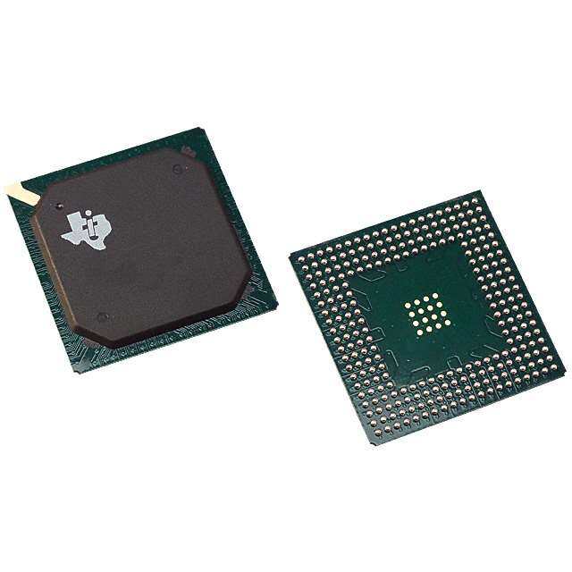
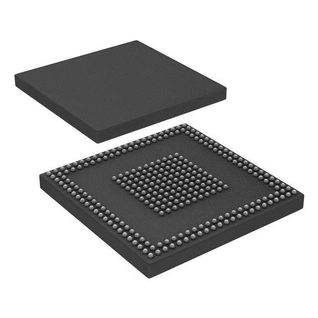
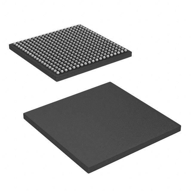
| 描述 | IC DSP 533MHZ W/DDR 400CSPBGA数字信号处理器和控制器 - DSP, DSC High Perf Convergent Multimedia Blackfin |
| 产品分类 | |
| 品牌 | Analog Devices Inc |
| MIPS | 533 MIPs |
| 产品手册 | |
| 产品图片 |
|
| rohs | 符合RoHS无铅 / 符合限制有害物质指令(RoHS)规范要求 |
| 产品系列 | 嵌入式处理器和控制器,数字信号处理器和控制器 - DSP, DSC,Analog Devices ADSP-BF548MBBCZ-5MBlackfin® |
| mouser_ship_limit | 此产品可能要求许可证才能从美国出口。 |
| 数据手册 | |
| 产品型号 | ADSP-BF548MBBCZ-5M |
| 产品种类 | 数字信号处理器和控制器 - DSP, DSC |
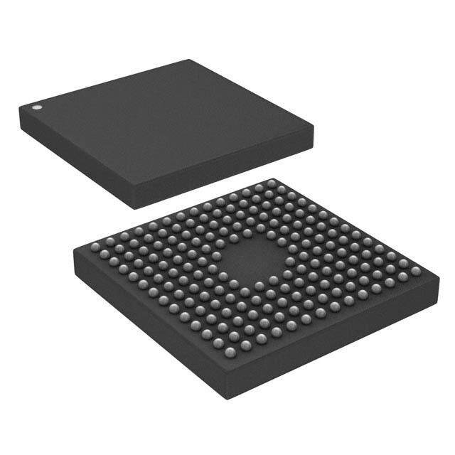
| 供应商器件封装 | 400-CSPBGA(17x17) |
| 其它名称 | ADSPBF548MBBCZ5M |
| 包装 | 托盘 |
| 商标 | Analog Devices |
| 商标名 | Blackfin |
| 安装类型 | 表面贴装 |
| 安装风格 | SMD/SMT |
| 定时器数量 | 11 |
| 封装 | Tray |
| 封装/外壳 | 400-LFBGA,CSPBGA |
| 封装/箱体 | BGA-400 |
| 工作温度 | -40°C ~ 85°C |
| 工作电源电压 | 2.5 V, 3.3 V |
| 工厂包装数量 | 90 |
| 接口 | CAN,SPI,SSP,TWI,UART,USB |
| 数据RAM大小 | 64 kB |
| 数据总线宽度 | 16 bit |
| 时钟速率 | 533MHz |
| 最大工作温度 | + 85 C |
| 最大时钟频率 | 533 MHz |
| 最小工作温度 | - 40 C |
| 标准包装 | 1 |
| 核心 | Blackfin |
| 片载RAM | 260kB |
| 电压-I/O | 2.50V,3.30V |
| 电压-内核 | 1.25V |
| 程序存储器大小 | 324 kB |
| 类型 | 定点 |
| 系列 | ADSP-BF548 |
| 非易失性存储器 | 外部 |


- 商务部:美国ITC正式对集成电路等产品启动337调查
- 曝三星4nm工艺存在良率问题 高通将骁龙8 Gen1或转产台积电
- 太阳诱电将投资9.5亿元在常州建新厂生产MLCC 预计2023年完工
- 英特尔发布欧洲新工厂建设计划 深化IDM 2.0 战略
- 台积电先进制程称霸业界 有大客户加持明年业绩稳了
- 达到5530亿美元!SIA预计今年全球半导体销售额将创下新高
- 英特尔拟将自动驾驶子公司Mobileye上市 估值或超500亿美元
- 三星加码芯片和SET,合并消费电子和移动部门,撤换高东真等 CEO
- 三星电子宣布重大人事变动 还合并消费电子和移动部门
- 海关总署:前11个月进口集成电路产品价值2.52万亿元 增长14.8%


PDF Datasheet 数据手册内容提取
Blackfin Embedded Processor ADSP-BF542/ADSP-BF544/ADSP-BF547/ADSP-BF548/ADSP-BF549 FEATURES PERIPHERALS Up to 600MHz high performance Blackfin processor High speed USB On-the-Go (OTG) with integrated PHY Two 16-bit MACs, two 40-bit ALUs, four 8-bit video ALUs SD/SDIO controller RISC-like register and instruction model ATA/ATAPI-6 controller Wide range of operating voltages and flexible booting Up to 4 synchronous serial ports (SPORTs) options Up to 3 serial peripheral interfaces (SPI-compatible) Programmable on-chip voltage regulator Up to 4 UARTs, two with automatic H/W flow control 400-ball CSP_BGA, RoHS compliant package Up to 2 CAN (controller area network) 2.0B interfaces MEMORY Up to 2 TWI (2-wire interface) controllers 8- or 16-bit asynchronous host DMA interface Up to 324K bytes of on-chip memory comprised of Multiple enhanced parallel peripheral interfaces (EPPIs), instruction SRAM/cache; dedicated instruction SRAM; data supporting ITU-R BT.656 video formats and 18-/24-bit LCD SRAM/cache; dedicated data SRAM; scratchpad SRAM connections External sync memory controller supporting either DDR Media transceiver (MXVR) for connection to a MOST network SDRAM or mobile DDR SDRAM Pixel compositor for overlays, alpha blending, and color External async memory controller supporting 8-/16-bit async conversion memories and burst flash devices Up to eleven 32-bit timers/counters with PWM support NAND flash controller Real-time clock (RTC) and watchdog timer 4 memory-to-memory DMA pairs, 2 with ext. requests Up/down counter with support for rotary encoder Memory management unit providing memory protection Up to 152 general-purpose I/O (GPIOs) Code security with Lockbox secure technology and 128-bit On-chip PLL capable of frequency multiplication AES/ARC4 data encryption Debug/JTAG interface One-time-programmable (OTP) memory CAN (0-1) REVGOULTLAAGTOER JTEAMGU TLEASTTI OANND RTC WATTICMHEDROG OTP TWI (0-1) PAB 16 B HOST DMA TIMERS(0-10) INTERRUPTS S UART (0-1) T R O COUNTER P UART (2-3) L2 L1 L1 L1 KEYPAD SRAM INSTRROM INSTRSRAM DATA SRAM SPI (0-1) S T SPI (2) R MXVR 32-BIT DMA PO DCB 32 EAB 64 DEB 32 DAB1 32 SPORT (2-3) USB 16-BIT DMA SPORT (0-1) DAB0 16 BOOT EXTERNAL PORT ROM NOR, DDR, MDDR SD / SDIO ATAPI DDR/MDDR ASYNC EPPI (0-2) 16 16 NAND FLASH PIXEL CONTROLLER COMPOSITOR Figure 1. ADSP-BF549 Functional Block Diagram Blackfin and the Blackfin logo are registered trademarks of Analog Devices, Inc. Rev. E Document Feedback Information furnished by Analog Devices is believed to be accurate and reliable. However, no responsibility is assumed by Analog Devices for its use, nor for any infringements of patents or other rights of third parties that may result from its use. Specifications subject to change without notice. No license is granted by implication One Technology Way, P.O. Box 9106, Norwood, MA 02062-9106 U.S.A. or otherwise under any patent or patent rights of Analog Devices. Trademarks and Tel: 781.329.4700 ©2014 Analog Devices, Inc. All rights reserved. registered trademarks are the property of their respective owners. Technical Support www.analog.com
ADSP-BF542/ADSP-BF544/ADSP-BF547/ADSP-BF548/ADSP-BF549 TABLE OF CONTENTS Features ................................................................. 1 Voltage Regulation .............................................. 16 Memory ................................................................ 1 Clock Signals ...................................................... 17 Peripherals ............................................................. 1 Booting Modes ................................................... 18 General Description ................................................. 3 Instruction Set Description .................................... 21 Low Power Architecture ......................................... 4 Development Tools .............................................. 21 System Integration ................................................ 4 MXVR Board Layout Guidelines ............................. 22 Blackfin Processor Peripherals ................................. 4 Additional information ......................................... 23 Blackfin Processor Core .......................................... 4 Related Signal Chains ........................................... 23 Memory Architecture ............................................ 6 Lockbox Secure Technology Disclaimer .................... 23 DMA Controllers .................................................. 9 Pin Descriptions .................................................... 24 Real-Time Clock ................................................. 10 Specifications ........................................................ 34 Watchdog Timer ................................................ 10 Operating Conditions ........................................... 34 Timers ............................................................. 10 Electrical Characteristics ....................................... 36 Up/Down Counter and Thumbwheel Interface .......... 11 Absolute Maximum Ratings ................................... 40 Serial Ports (SPORTs) .......................................... 11 ESD Sensitivity ................................................... 41 Serial Peripheral Interface (SPI) Ports ...................... 11 Package Information ............................................ 41 UART Ports (UARTs) .......................................... 11 Timing Specifications ........................................... 42 Controller Area Network (CAN) ............................ 12 Output Drive Currents ......................................... 88 TWI Controller Interface ...................................... 12 Test Conditions .................................................. 90 Ports ................................................................ 12 Capacitive Loading .............................................. 90 Pixel Compositor (PIXC) ...................................... 13 Typical Rise and Fall Times ................................... 91 Enhanced Parallel Peripheral Interface (EPPI) ........... 13 Thermal Characteristics ........................................ 93 USB On-the-Go Dual-Role Device Controller ............ 13 400-Ball CSP_BGA Package ...................................... 94 ATA/ATAPI-6 Interface ....................................... 14 Outline Dimensions .............................................. 100 Keypad Interface ................................................. 14 Surface-Mount Design ........................................ 100 Secure Digital (SD)/SDIO Controller ....................... 14 Automotive Products ............................................ 101 Code Security .................................................... 14 Ordering Guide ................................................... 101 Media Transceiver MAC Layer (MXVR) .................. 14 Dynamic Power Management ................................ 15 REVISION HISTORY 03/14—Rev. D to Rev. E Added/changed package dimensions to Figure 88 in Outline Dimensions .............................................. 100 Updated Development Tools .................................... 21 Added low Alpha Package model to Ordering Guide ..... 101 Corrected SPI2 pin count in Port B configuration in Pin Multiplexing .................................................... 24 Corrected typographical error of parameter name in External DMA Request Timing ................................. 58 Added note to Table 42 in Serial Ports—Enable and Three-State .......................... 63 Corrected t and t minimum specifications from t +1 to WL WH SCLK 1 × t in Timer Cycle Timing ................................. 69 SCLK Rev. E | Page 2 of 102 | March 2014
ADSP-BF542/ADSP-BF544/ADSP-BF547/ADSP-BF548/ADSP-BF549 GENERAL DESCRIPTION The ADSP-BF54x Blackfin® processors are members of the Specific peripherals for ADSP-BF54x Blackfin processors are Blackfin family of products, incorporating the Analog Devices/ shown in Table2. Intel Micro Signal Architecture (MSA). Blackfin processors combine a dual-MAC state-of-the-art signal processing engine, Table 2. Specific Peripherals for ADSP-BF54x Processors the advantages of a clean, orthogonal RISC-like microprocessor instruction set, and single-instruction, multiple-data (SIMD) 9 8 7 4 2 4 4 4 4 4 multimedia capabilities into a single instruction-set 5 5 5 5 5 F F F F F architecture. B B B B B P- P- P- P- P- Specific performance, memory configurations, and features of DS DS DS DS DS ADSP-BF54x Blackfin processors are shown in Table1. Module A A A A A EBIU (async) P P P P P Table 1. ADSP-BF54x Processor Features NAND flash controller P P P P P ATAPI P P P – P 9 8 7 4 2 4 4 4 4 4 5 5 5 5 5 Host DMA port (HOSTDP) P P P P – F F F F F B B B B B P- P- P- P- P- SD/SDIO controller P P P – P S S S S S D D D D D EPPI0 P P P P – Processor Features A A A A A EPPI1 P P P P P Lockbox® 1code security 1 1 1 1 1 EPPI2 P P P P P 128-bit AES/ ARC4 data encryption 1 1 1 1 1 SPORT0 P P P – – SD/SDIO controller 1 1 1 – 1 SPORT1 P P P P P Pixel compositor 1 1 1 1 1 SPORT2 P P P P P 18- or 24-bit EPPI0 with LCD 1 1 1 1 – SPORT3 P P P P P 16-bit EPPI1, 8-bit EPPI2 1 1 1 1 1 SPI0 P P P P P Host DMA port 1 1 1 1 – SPI1 P P P P P NAND flash controller 1 1 1 1 1 SPI2 P P P – – ATAPI 1 1 1 – 1 UART0 P P P P P High speed USB OTG 1 1 1 – 1 UART1 P P P P P Keypad interface 1 1 1 – 1 UART2 P P P – – MXVR 1 – – – – UART3 P P P P P CAN ports 2 2 – 2 1 High speed USB OTG P P P – P TWI ports 2 2 2 2 1 CAN0 P P – P P SPI ports 3 3 3 2 2 CAN1 P P – P – UART ports 4 4 4 3 3 TWI0 P P P P P SPORTs 4 4 4 3 3 TWI1 P P P P – Up/down counter 1 1 1 1 1 Timer 0–7 P P P P P Timers 11 11 11 11 8 Timer 8–10 P P P P – General-purpose I/O pins 152 152 152 152 152 Up/down counter P P P P P Memory L1 Instruction SRAM/cache 16 16 16 16 16 Configura- L1 Instruction SRAM 48 48 48 48 48 Keypad interface P P P – P tions MXVR P – – – – L1 Data SRAM/cache 32 32 32 32 32 (K Bytes) GPIOs P P P P P L1 Data SRAM 32 32 32 32 32 L1 Scratchpad SRAM 4 4 4 4 4 L1 ROM2 64 64 64 64 64 L2 128 128 128 64 – L3 Boot ROM2 4 4 4 4 4 Maximum core instruction rate (MHz) 533 533 600 533 600 1Lockbox is a registered trademark of Analog Devices, Inc. 2This ROM is not customer-configurable. Rev. E | Page 3 of 102 | March 2014
ADSP-BF542/ADSP-BF544/ADSP-BF547/ADSP-BF548/ADSP-BF549 The ADSP-BF54x Blackfin processors are completely code- and memory spaces, including external DDR (either standard or pin-compatible. They differ only with respect to their perfor- mobile, depending on the device) and asynchronous memory. mance, on-chip memory, and selection of I/O peripherals. Multiple on-chip buses running at up to 133MHz provide Specific performance, memory, and feature configurations are enough bandwidth to keep the processor core running along shown in Table1. with activity on all of the on-chip and external peripherals. By integrating a rich set of industry-leading system peripherals The ADSP-BF54x Blackfin processors include an on-chip volt- and memory, Blackfin processors are the platform of choice for age regulator in support of the dynamic power management next-generation applications that require RISC-like program- capability. The voltage regulator provides a range of core volt- mability, multimedia support, and leading-edge signal age levels when supplied from V . The voltage regulator can DDEXT processing in one integrated package. be bypassed at the user’s discretion. LOW POWER ARCHITECTURE BLACKFIN PROCESSOR CORE Blackfin processors provide world-class power management As shown in Figure2 on Page5, the Blackfin processor core and performance. Blackfin processors are designed in a low contains two 16-bit multipliers, two 40-bit accumulators, two power and low voltage design methodology and feature on-chip 40-bit ALUs, four video ALUs, and a 40-bit shifter. The compu- dynamic power management, the ability to vary both the voltage tation units process 8-, 16-, or 32-bit data from the register file. and frequency of operation to significantly lower overall power The compute register file contains eight 32-bit registers. When consumption. Reducing both voltage and frequency can result performing compute operations on 16-bit operand data, the in a substantial reduction in power consumption as compared register file operates as 16 independent 16-bit registers. All to reducing only the frequency of operation. This translates into operands for compute operations come from the multiported longer battery life for portable appliances. register file and instruction constant fields. SYSTEM INTEGRATION Each MAC can perform a 16-bit by 16-bit multiply in each cycle, accumulating the results into the 40-bit accumulators. The ADSP-BF54x Blackfin processors are highly integrated Signed and unsigned formats, rounding, and saturation are system-on-a-chip solutions for the next generation of embed- supported. ded network connected applications. By combining industry- standard interfaces with a high performance signal processing The ALUs perform a traditional set of arithmetic and logical core, users can develop cost-effective solutions quickly without operations on 16- or 32-bit data. In addition, many special the need for costly external components. The system peripherals instructions are included to accelerate various signal processing include a high speed USB OTG (On-the-Go) controller with tasks. These include bit operations such as field extract and pop- integrated PHY, CAN 2.0B controllers, TWI controllers, UART ulation count, modulo 232 multiply, divide primitives, saturation ports, SPI ports, serial ports (SPORTs), ATAPI controller, and rounding, and sign/exponent detection. The set of video SD/SDIO controller, a real-time clock, a watchdog timer, LCD instructions include byte alignment and packing operations, controller, and multiple enhanced parallel peripheral interfaces. 16-bit and 8-bit adds with clipping, 8-bit average operations, and 8-bit subtract/absolute value/accumulate (SAA) operations. BLACKFIN PROCESSOR PERIPHERALS Also provided are the compare/select and vector search The ADSP-BF54x processors contain a rich set of peripherals instructions. connected to the core via several high bandwidth buses, provid- For certain instructions, two 16-bit ALU operations can be per- ing flexibility in system configuration as well as excellent overall formed simultaneously on register pairs (a 16-bit high half and system performance (see Figure1 on Page1). The general- 16-bit low half of a compute register). By also using the second purpose peripherals include functions such as UARTs, SPI, ALU, quad 16-bit operations are possible. TWI, timers with pulse width modulation (PWM) and pulse The 40-bit shifter can perform shifts and rotates and is used to measurement capability, general-purpose I/O pins, a real-time support normalization, field extract, and field deposit clock, and a watchdog timer. This set of functions satisfies a instructions. wide variety of typical system support needs and is augmented by the system expansion capabilities of the part. The ADSP- The program sequencer controls the flow of instruction execu- BF54x processors contain dedicated network communication tion, including instruction alignment and decoding. For modules and high speed serial and parallel ports, an interrupt program flow control, the sequencer supports PC relative and controller for flexible management of interrupts from the on- indirect conditional jumps (with static branch prediction), and chip peripherals or external sources, and power management subroutine calls. Hardware is provided to support zero-over- control functions to tailor the performance and power charac- head looping. The architecture is fully interlocked, meaning that teristics of the processor and system to many application the programmer need not manage the pipeline when executing scenarios. instructions with data dependencies. All of the peripherals, except for general-purpose I/O, CAN, The address arithmetic unit provides two addresses for simulta- TWI, real-time clock, and timers, are supported by a flexible neous dual fetches from memory. It contains a multiported DMA structure. There are also separate memory DMA channels register file consisting of four sets of 32-bit index, modify, dedicated to data transfers between the processor's various Rev. E | Page 4 of 102 | March 2014
ADSP-BF542/ADSP-BF544/ADSP-BF547/ADSP-BF548/ADSP-BF549 length, and base registers (for circular buffering), and eight The architecture provides three modes of operation: user mode, additional 32-bit pointer registers (for C-style indexed stack supervisor mode, and emulation mode. User mode has manipulation). restricted access to certain system resources, thus providing a protected software environment, while supervisor mode has Blackfin processors support a modified Harvard architecture in unrestricted access to the system and core resources. combination with a hierarchical memory structure. Level 1 (L1) memories are those that typically operate at the full processor The Blackfin processor instruction set has been optimized so speed with little or no latency. At the L1 level, the instruction that 16-bit opcodes represent the most frequently used instruc- memory holds instructions only. The two data memories hold tions, resulting in excellent compiled code density. Complex data, and a dedicated scratchpad data memory stores stack and DSP instructions are encoded into 32-bit opcodes, representing local variable information. fully featured multifunction instructions. Blackfin processors support a limited multi-issue capability, where a 32-bit instruc- In addition, multiple L1 memory blocks are provided, offering a tion can be issued in parallel with two 16-bit instructions, configurable mix of SRAM and cache. The memory manage- allowing the programmer to use many of the core resources in a ment unit (MMU) provides memory protection for individual single instruction cycle. tasks that may be operating on the core and can protect system registers from unintended access. The Blackfin processor assembly language uses an algebraic syn- tax for ease of coding and readability. The architecture has been optimized for use in conjunction with the C/C++compiler, resulting in fast and efficient software implementations. ADDRESS ARITHMETIC UNIT SP I3 L3 B3 M3 FP I2 L2 B2 M2 P5 I1 L1 B1 M1 DAG1 P4 I0 L0 B0 M0 P3 DAG0 P2 DA1 32 P1 DA0 32 P0 RY 32 32 MO RAB PREG E M O T SD 32 LD1 32 32 ASTAT LD0 32 32 SEQUENCER R7.H R7.L R6.H R6.L R5.H R5.L 16 16 ALIGN R4.H R4.L 8 8 8 8 R3.H R3.L R2.H R2.L DECODE R1.H R1.L BARREL R0.H R0.L SHIFTER 40 40 LOOP BUFFER 40 40 A0 A1 CONTROL UNIT 32 32 DATA ARITHMETIC UNIT Figure 2. Blackfin Processor Core Rev. E | Page 5 of 102 | March 2014
ADSP-BF542/ADSP-BF544/ADSP-BF547/ADSP-BF548/ADSP-BF549 MEMORY ARCHITECTURE The ADSP-BF54x processors view memory as a single unified 0xFFFFFFFF CORE MMR REGISTERS (2M BYTES) 4Gbyte address space, using 32-bit addresses. All resources, 0xFFE0 0000 including internal memory, external memory, and I/O control SYSTEM MMR REGISTERS (2M BYTES) 0xFFC0 0000 registers, occupy separate sections of this common address RESERVED 0xFFB0 1000 space. The memory portions of this address space are arranged SCRATCHPAD SRAM (4K BYTES) in a hierarchical structure to provide a good cost/performance 0xFFB0 0000 RESERVED balance of some very fast, low-latency on-chip memory as cache 0xFFA2 4000 L1ROM (64K BYTE) or SRAM, and larger, lower-cost and performance off-chip 0xFFA1 4000 memory systems. See Figure3 on Page6. INSTRUCTION SRAM / CACHE (16K BYTES) 0xFFA1 0000 The on-chip L1 memory system is the highest-performance RESERVED AP 0xFFA0C000 M memory available to the Blackfin processor. The off-chip mem- INSTRUCTION BANK B SRAM (16K BYTES) Y ory system, accessed through the external bus interface unit 0xFFA0 8000 INSTRUCTION BANK A SRAM (32K BYTES) MOR E (EBIU), provides expansion with flash memory, SRAM, and 0xFFA0 0000 M RESERVED L double-rate SDRAM (standard or mobile DDR), optionally 0xFF90 8000 NA accessing up to 768Mbytes of physical memory. 0xFF90 4000 DATA BANK B SRAM / CACHE (16K BYTES) TER DATABANKBSRAM (16KBYTES) N Most of the ADSP-BF54x Blackfin processors also include an L2 I 0xFF90 0000 SRAM memory array which provides up to 128K bytes of high RESERVED 0xFF80 8000 speed SRAM, operating at one half the frequency of the core and DATA BANK A SRAM / CACHE (16K BYTES) 0xFF80 4000 with slightly longer latency than the L1 memory banks (for DATABANKASRAM (16KBYTES) information on L2 memory in each processor, see Table1). The 0xFF80 0000 RESERVED L2 memory is a unified instruction and data memory and can 0xFEB2 0000 hold any mixture of code and data required by the system L2SRAM (128K BYTES) 0xFEB0 0000 design. The Blackfin cores share a dedicated low latency 64-bit RESERVED 0xEF00 1000 data path port into the L2 SRAM memory. BOOTROM (4K BYTES) 0xEF00 0000 The memory DMA controllers (DMAC1 and DMAC0) provide RESERVED 0x3000 0000 high-bandwidth data-movement capability. They can perform ASYNC MEMORY BANK 3 (64M BYTES) AP block transfers of code or data between the internal memory 0x2C00 0000 M ASYNC MEMORY BANK 2 (64M BYTES) Y and the external memory spaces. 0x2800 0000 OR ASYNC MEMORY BANK 1 (64M BYTES) M Internal (On-Chip) Memory 0x2400 0000 ME ASYNC MEMORY BANK 0 (64M BYTES) L The ADSP-BF54x processors have several blocks of on-chip T0Ox2P0 O00F 0L0A0S0T RESERVED ERNA memory providing high bandwidth access to the core. DDR PAGE DDR MEM BANK 1 (8M BYTES to 256M BYTES) EXT The first block is the L1 instruction memory, consisting of DDR MEM BANK 0 (8M BYTES to 256M BYTES) 64Kbytes of SRAM, of which 16Kbytes can be configured as a 0x0000 0000 four-way set-associative cache or as SRAM. This memory is accessed at full processor speed. Figure 3. ADSP-BF547/ADSP-BF548/ADSP-BF549 The second on-chip memory block is the L1 data memory, con- Internal/External Memory Map1 sisting of 64Kbytes of SRAM, of which 32K bytes can be 1For ADSP-BF544 processors, L2 SRAM is 64K Bytes configured as a two-way set-associative cache or as SRAM. This (0xFEB0000–0xFEB0FFFF). For ADSP-BF542 processors, there is no L2 memory block is accessed at full processor speed. SRAM. The third memory block is a 4Kbyte scratchpad SRAM, which External (Off-Chip) Memory runs at the same speed as the L1 memories. It is only accessible as data SRAM and cannot be configured as cache memory. Through the external bus interface unit (EBIU), the ADSP-BF54x Blackfin processors provide glueless connectivity The fourth memory block is the factory programmed L1 to external 16-bit wide memories, such as DDR and mobile instruction ROM, operating at full processor speed. This ROM DDR SDRAM, SRAM, NOR flash, NAND flash, and FIFO is not customer-configurable. devices. To provide the best performance, the bus system of the The fifth memory block is the L2 SRAM, providing up to 128K DDR and mobile DDR interface is completely separate from the bytes of unified instruction and data memory, operating at one other parallel interfaces. Furthermore, the DDR controller sup- half the frequency of the core. ports either standard DDR memory or mobile DDR memory. Finally, there is a 4K byte boot ROM connected as L3 memory. See the Ordering Guide on Page101 for details. Throughout It operates at full SCLK rate. this document, references to “DDR” are intended to cover both the standard and mobile DDR standards. Rev. E | Page 6 of 102 | March 2014
ADSP-BF542/ADSP-BF544/ADSP-BF547/ADSP-BF548/ADSP-BF549 The DDR memory controller can gluelessly manage up to two • Support for SLC (single level cell) NAND flash devices banks of double-rate synchronous dynamic memory (DDR and unlimited in size, with page sizes of 256 bytes and 512 mobile DDR SDRAM). The 16-bit interface operates at the bytes. Larger page sizes can be supported in software. SCLK frequency, enabling a maximum throughput of 532M • The ability to release external bus interface pins during bytes/s. The DDR and mobile DDR controller is augmented long accesses. with a queuing mechanism that performs efficient bursts into the DDR and mobile DDR. The controller is an industry stan- • Support for internal bus requests of 16 bits or 32 bits. dard DDR and mobile DDR SDRAM controller with each bank • A DMA engine to transfer data between internal memory supporting from 64M bit to 512M bit device sizes and 4-, 8-, or and a NAND flash device. 16-bit widths. The controller supports up to 256M bytes per One-Time-Programmable Memory external bank. With 2 external banks, the controller supports up to 512M bytes total. Each bank is independently programmable The ADSP-BF54x Blackfin processors have 64K bits of one- and is contiguous with adjacent banks regardless of the sizes of time-programmable (OTP) non-volatile memory that can be the different banks or their placement. programmed by the developer only one time. It includes the Traditional 16-bit asynchronous memories, such as SRAM, array and logic to support read access and programming. Addi- EPROM, and flash devices, can be connected to one of the four tionally, its pages can be write protected. 64M byte asynchronous memory banks, represented by four OTP enables developers to store both public and private data memory select strobes. Alternatively, these strobes can function on-chip. In addition to storing public and private key data for as bank-specific read or write strobes preventing further glue applications requiring security, it also allows developers to store logic when connecting to asynchronous FIFO devices. See the completely user-definable data such as a customer ID, product Ordering Guide on Page101 for a list of specific products that ID, or a MAC address. By using this feature, generic parts can be provide support for DDR memory. shipped, which are then programmed and protected by the In addition, the external bus can connect to advanced flash developer within this non-volatile memory. The OTP memory device technologies, such as: can be accessed through an API provided by the on-chip ROM. • Page-mode NOR flash devices I/O Memory Space • Synchronous burst-mode NOR flash devices The ADSP-BF54x Blackfin processors do not define a separate • NAND flash devices I/O space. All resources are mapped through the flat 32-bit address space. On-chip I/O devices have their control registers Customers should consult the Ordering Guide when selecting a mapped into memory-mapped registers (MMRs) at addresses specific ADSP-BF54x component for the intended application. near the top of the 4Gbyte address space. These are separated Products that provide support for mobile DDR memory are into two smaller blocks, one containing the control MMRs for noted in the ordering guide footnotes. all core functions and the other containing the registers needed NAND Flash Controller (NFC) for setup and control of the on-chip peripherals outside of the core. The MMRs are accessible only in supervisor mode and The ADSP-BF54x Blackfin processors provide a NAND Flash appear as reserved space to on-chip peripherals. Controller (NFC) as part of the external bus interface. NAND flash devices provide high-density, low-cost memory. However, Booting NAND flash devices also have long random access times, invalid The ADSP-BF54x Blackfin processors contain a small on-chip blocks, and lower reliability over device lifetimes. Because of boot kernel, which configures the appropriate peripheral for this, NAND flash is often used for read-only code storage. In booting. If the ADSP-BF54x Blackfin processors are configured this case, all DSP code can be stored in NAND flash and then to boot from boot ROM memory space, the processor starts exe- transferred to a faster memory (such as DDR or SRAM) before cuting from the on-chip boot ROM. For more information, see execution. Another common use of NAND flash is for storage Booting Modes on Page18. of multimedia files or other large data segments. In this case, a software file system may be used to manage reading and writing Event Handling of the NAND flash device. The file system selects memory seg- The event controller on the ADSP-BF54x Blackfin processors ments for storage with the goal of avoiding bad blocks and handles all asynchronous and synchronous events to the proces- equally distributing memory accesses across all address loca- sors. The ADSP-BF54x Blackfin processors provide event tions. Hardware features of the NFC include: handling that supports both nesting and prioritization. Nesting • Support for page program, page read, and block erase of allows multiple event service routines to be active simultane- NAND flash devices, with accesses aligned to page ously. Prioritization ensures that servicing of a higher-priority boundaries. event takes precedence over servicing of a lower-priority event. • Error checking and correction (ECC) hardware that facili- tates error detection and correction. • A single 8-bit or 16-bit external bus interface for com- mands, addresses, and data. Rev. E | Page 7 of 102 | March 2014
ADSP-BF542/ADSP-BF544/ADSP-BF547/ADSP-BF548/ADSP-BF549 The controller provides support for five different types of Table 3. Core Event Controller (CEC) events: Priority • Emulation. An emulation event causes the processor to (0 is Highest) Event Class EVT Entry enter emulation mode, allowing command and control of 0 Emulation/Test Control EMU the processor via the JTAG interface. 1 Reset RST • Reset. This event resets the processor. 2 Nonmaskable Interrupt NMI • Non-maskable interrupt (NMI). The NMI event can be 3 Exception EVX generated by the software watchdog timer or by the NMI input signal to the processor. The NMI event is frequently 4 Reserved — used as a power-down indicator to initiate an orderly shut- 5 Hardware Error IVHW down of the system. 6 Core Timer IVTMR • Exceptions. Events that occur synchronously to program 7 General Interrupt 7 IVG7 flow (that is, the exception is taken before the instruction is 8 General Interrupt 8 IVG8 allowed to complete). Conditions such as data alignment 9 General Interrupt 9 IVG9 violations and undefined instructions cause exceptions. 10 General Interrupt 10 IVG10 • Interrupts. Events that occur asynchronously to program 11 General Interrupt 11 IVG11 flow. They are caused by input pins, timers, and other 12 General Interrupt 12 IVG12 peripherals, as well as by an explicit software instruction. 13 General Interrupt 13 IVG13 Each event type has an associated register to hold the return address and an associated return-from-event instruction. When 14 General Interrupt 14 IVG14 an event is triggered, the state of the processor is saved on the 15 General Interrupt 15 IVG15 supervisor stack. Event Control The ADSP-BF54x Blackfin processor event controller consists of two stages, the core event controller (CEC) and the system The ADSP-BF54x Blackfin processors provide the user with a interrupt controller (SIC). The core event controller works with very flexible mechanism to control the processing of events. In the system interrupt controller to prioritize and control all sys- the CEC, three registers are used to coordinate and control tem events. Conceptually, interrupts from the peripherals enter events. Each register is 16 bits wide: into the SIC and are then routed directly into the general-pur- • CEC interrupt latch register (ILAT). The ILAT register pose interrupts of the CEC. indicates when events have been latched. The appropriate Core Event Controller (CEC) bit is set when the processor has latched the event and cleared when the event has been accepted into the system. The CEC supports nine general-purpose interrupts (IVG15–7), This register is updated automatically by the controller, but in addition to the dedicated interrupt and exception events. Of it may be written only when its corresponding IMASK bit these general-purpose interrupts, the two lowest-priority inter- is cleared. rupts (IVG15–14) are recommended to be reserved for software • CEC interrupt mask register (IMASK). The IMASK regis- interrupt handlers, leaving seven prioritized interrupt inputs to ter controls the masking and unmasking of individual support the peripherals of the ADSP-BF54x Blackfin processors. events. When a bit is set in the IMASK register, that event is Table3 describes the inputs to the CEC, identifies their names unmasked and is processed by the CEC when asserted. A in the event vector table (EVT), and lists their priorities. cleared bit in the IMASK register masks the event, prevent- System Interrupt Controller (SIC) ing the processor from servicing the event even though the event may be latched in the ILAT register. This register The system interrupt controller provides the mapping and rout- may be read or written while in supervisor mode. Note that ing of events from the many peripheral interrupt sources to the general-purpose interrupts can be globally enabled and dis- prioritized general-purpose interrupt inputs of the CEC. abled with the STI and CLI instructions, respectively. Although the ADSP-BF54x Blackfin processors provide a default mapping, the user can alter the mappings and priorities • CEC interrupt pending register (IPEND). The IPEND reg- of interrupt events by writing the appropriate values into the ister keeps track of all nested events. A set bit in the IPEND interrupt assignment registers (SIC_IARx). The ADSP-BF54x register indicates that the event is currently active or nested Hardware Reference Manual, “System Interrupts” chapter at some level. This register is updated automatically by the describes the inputs into the SIC and the default mappings into controller but may be read while in supervisor mode. the CEC. The SIC allows further control of event processing by providing three 32-bit interrupt control and status registers. Each register contains a bit corresponding to each of the peripheral interrupt events shown in the ADSP-BF54x Hardware Reference Manual, “System Interrupts” chapter. Rev. E | Page 8 of 102 | March 2014
ADSP-BF542/ADSP-BF544/ADSP-BF547/ADSP-BF548/ADSP-BF549 • SIC interrupt mask registers (SIC_IMASKx). These regis- DAB16 bus. Individual DMA channels have fixed access prior- ters control the masking and unmasking of each peripheral ity on the DAB buses. DMA priority of peripherals is managed interrupt event. When a bit is set in a register, that periph- by a flexible peripheral-to-DMA channel assignment scheme. eral event is unmasked and is processed by the system All four DMA controllers use the same 32-bit DCB bus to when asserted. A cleared bit in the register masks the exchange data with L1 memory. This includes L1 ROM, but peripheral event, preventing the processor from servicing excludes scratchpad memory. Fine granulation of L1 memory the event. and special DMA buffers minimize potential memory conflicts • SIC interrupt status registers (SIC_ISRx). As multiple when the L1 memory is accessed simultaneously by the core. peripherals can be mapped to a single event, these registers Similarly, there are dedicated DMA buses between the external allow the software to determine which peripheral event bus interface unit (EBIU) and the three DMA controllers source triggered the interrupt. A set bit indicates the (DMAC1, DMAC0, and USB) that arbitrate DMA accesses to peripheral is asserting the interrupt, and a cleared bit indi- external memories and the boot ROM. cates the peripheral is not asserting the event. The ADSP-BF54x Blackfin processors’ DMA controllers sup- • SIC interrupt wakeup enable registers (SIC_IWRx). By port both 1-dimensional (1D) and 2-dimensional (2D) DMA enabling the corresponding bit in this register, a peripheral transfers. DMA transfer initialization can be implemented from can be configured to wake up the processor, should the registers or from sets of parameters called descriptor blocks. core be idled or in Sleep mode when the event is generated. The 2D DMA capability supports arbitrary row and column (For more information, see Dynamic Power Management sizes up to 64K elements by 64K elements, and arbitrary row on Page15.) and column step sizes up to ±32K elements. Furthermore, the Because multiple interrupt sources can map to a single general- column step size can be less than the row step size, allowing purpose interrupt, multiple pulse assertions can occur simulta- implementation of interleaved data streams. This feature is neously, before or during interrupt processing for an interrupt especially useful in video applications where data can be de- event already detected on this interrupt input. The IPEND reg- interleaved on the fly. ister contents are monitored by the SIC as the interrupt Examples of DMA types supported by the ADSP-BF54x Black- acknowledgement. fin processors’ DMA controllers include: The appropriate ILAT register bit is set when an interrupt rising • A single, linear buffer that stops upon completion edge is detected. (Detection requires two core clock cycles.) The bit is cleared when the respective IPEND register bit is set. The • A circular, auto-refreshing buffer that interrupts on each IPEND bit indicates that the event has entered into the proces- full or fractionally full buffer sor pipeline. At this point the CEC recognizes and queues the • 1D or 2D DMA using a linked list of descriptors next rising edge event on the corresponding event input. The • 2D DMA using an array of descriptors, specifying only the minimum latency from the rising edge transition of the general- base DMA address within a common page purpose interrupt to the IPEND output asserted is three core clock cycles; however, the latency can be much higher, depend- In addition to the dedicated peripheral DMA channels, the ing on the activity within and the state of the processor. DMAC1 and DMAC0 controllers each feature two memory DMA channel pairs for transfers between the various memories DMA CONTROLLERS of the ADSP-BF54x Blackfin processors. This enables transfers of blocks of data between any of the memories—including ADSP-BF54x Blackfin processors have multiple, independent external DDR, ROM, SRAM, and flash memory—with minimal DMA channels that support automated data transfers with min- processor intervention. Like peripheral DMAs, memory DMA imal overhead for the processor core. DMA transfers can occur transfers can be controlled by a very flexible descriptor-based between the ADSP-BF54x processors’ internal memories and methodology or by a standard register-based autobuffer any of the DMA-capable peripherals. Additionally, DMA trans- mechanism. fers can be accomplished between any of the DMA-capable peripherals and external devices connected to the external The memory DMA channels of the DMAC1 controller memory interfaces, including DDR and asynchronous memory (MDMA2 and MDMA3) can be controlled optionally by the controllers. external DMA request input pins. When used in conjunction with the External Bus Interface Unit (EBIU), this handshaked While the USB controller and MXVR have their own dedicated memory DMA (HMDMA) scheme can be used to efficiently DMA controllers, the other on-chip peripherals are managed by exchange data with block-buffered or FIFO-style devices con- two centralized DMA controllers, called DMAC1 (32-bit) and nected externally. Users can select whether the DMA request DMAC0 (16-bit). Both operate in the SCLK domain. Each DMA pins control the source or the destination side of the memory controller manages 12 independent peripheral DMA channels, DMA. It allows control of the number of data transfers for as well as two independent memory DMA streams. The memory DMA. The number of transfers per edge is program- DMAC1 controller masters high-bandwidth peripherals over a mable. This feature can be programmed to allow memory DMA dedicated 32-bit DMA access bus (DAB32). Similarly, the to have an increased priority on the external bus relative to the DMAC0 controller masters most serial interfaces over the 16-bit core. Rev. E | Page 9 of 102 | March 2014
ADSP-BF542/ADSP-BF544/ADSP-BF547/ADSP-BF548/ADSP-BF549 Host DMA Port Interface wake up the ADSP-BF54x processors from deep sleep mode, and it can wake up the on-chip internal voltage regulator from The host DMA port (HOSTDP) facilitates a host device external the hibernate state. to the ADSP-BF54x Blackfin processors to be a DMA master and transfer data back and forth. The host device always masters Connect RTC pins RTXI and RTXO with external components the transactions, and the processor is always a DMA slave as shown in Figure4. device. The HOSTDP is enabled through the peripheral access bus. Once the port has been enabled, the transactions are controlled RTXI RTXO by the external host. The external host programs standard DMA R1 configuration words in order to send/receive data to any valid internal or external memory location. The host DMA port con- X1 troller includes the following features: C1 C2 • Allows an external master to configure DMA read/write data transfers and read port status • Uses a flexible asynchronous memory protocol for its external interface SUGGESTEDCOMPONENTS: ECLIPTEKEC38J(THROUGH-HOLEPACKAGE) EPSONMC40512pFLOAD(SURFACE-MOUNT PACKAGE) • Allows an 8- or 16-bit external data interface to the host C1=22pF device CR21==2120pMFΩ NOTE:C1ANDC2ARESPECIFICTOCRYSTALSPECIFIEDFORX1. • Supports half-duplex operation CONTACTCRYSTALMANUFACTURERFORDETAILS.C1ANDC2 SPECIFICATIONSASSUMEBOARDTRACECAPACITANCEOF3pF. • Supports little/big endian data transfers • Acknowledge mode allows flow control on host Figure 4. External Components for RTC transactions • Interrupt mode guarantees a burst of FIFO depth host WATCHDOG TIMER transactions The ADSP-BF54x processors include a 32-bit timer that can be REAL-TIME CLOCK used to implement a software watchdog function. A software watchdog can improve system reliability by forcing the proces- The ADSP-BF54x Blackfin processors’ real-time clock (RTC) sor to a known state through generation of a hardware reset, provides a robust set of digital watch features, including current non-maskable interrupt (NMI), or general-purpose interrupt if time, stopwatch, and alarm. The RTC is clocked by a 32.768kHz the timer expires before being reset by software. The program- crystal external to the ADSP-BF54x Blackfin processors. The mer initializes the count value of the timer, enables the RTC peripheral has dedicated power supply pins so that it can appropriate interrupt, and then enables the timer. Thereafter, remain powered up and clocked even when the rest of the pro- the software must reload the counter before it counts to zero cessor is in a low-power state. The RTC provides several from the programmed value. This protects the system from programmable interrupt options, including interrupt per sec- remaining in an unknown state where software, which would ond, minute, hour, or day clock ticks, interrupt on normally reset the timer, has stopped running due to an external programmable stopwatch countdown, or interrupt at a pro- noise condition or software error. grammed alarm time. If configured to generate a hardware reset, the watchdog timer The 32.768kHz input clock frequency is divided down to a 1Hz resets both the core and the ADSP-BF54x processors’ peripher- signal by a prescaler. The counter function of the timer consists als. After a reset, software can determine if the watchdog was the of four counters: a 60-second counter, a 60-minute counter, a source of the hardware reset by interrogating a status bit in the 24-hour counter, and a 32,768-day counter. watchdog timer control register. When enabled, the alarm function generates an interrupt when The timer is clocked by the system clock (SCLK) at a maximum the output of the timer matches the programmed value in the frequency of f . alarm control register. There are two alarms. The first alarm is SCLK for a time of day. The second alarm is for a day and time of TIMERS that day. There are up to two timer units in the ADSP-BF54x Blackfin The stopwatch function counts down from a programmed value processors. One unit provides eight general-purpose program- with one-second resolution. When the stopwatch is enabled and mable timers, and the other unit provides three. Each timer has the counter underflows, an interrupt is generated. an external pin that can be configured either as a pulse width Like the other peripherals, the RTC can wake up the modulator (PWM) or timer output, as an input to clock the ADSP-BF54x processor from sleep mode upon generation of timer, or as a mechanism for measuring pulse widths and peri- any RTC wakeup event. Additionally, an RTC wakeup event can ods of external events. These timers can be synchronized to an external clock input on the TMRx pins, an external clock TMRCLK input pin, or to the internal SCLK. Rev. E | Page 10 of 102 | March 2014
ADSP-BF542/ADSP-BF544/ADSP-BF547/ADSP-BF548/ADSP-BF549 The timer units can be used in conjunction with the four • Companding in hardware. Each SPORT can perform UARTs and the CAN controllers to measure the width of the A-law or μ-law companding according to ITU recommen- pulses in the data stream to provide a software auto-baud detect dation G.711. Companding can be selected on the transmit function for the respective serial channels. and/or receive channel of the SPORT without additional latencies. The timers can generate interrupts to the processor core, pro- viding periodic events for synchronization to either the system • DMA operations with single-cycle overhead. Each SPORT clock or to a count of external signals. can receive and transmit multiple buffers of memory data automatically. The processor can link or chain sequences of In addition to the general-purpose programmable timers, DMA transfers between a SPORT and memory. another timer is also provided by the processor core. This extra timer is clocked by the internal processor clock and is typically • Interrupts. Each transmit and receive port generates an used as a system tick clock for generation of periodic operating interrupt upon completing the transfer of a data word or system interrupts. after transferring an entire data buffer or buffers through DMA. UP/DOWN COUNTER AND THUMBWHEEL • Multichannel capability. Each SPORT supports 128 chan- INTERFACE nels out of a 1024-channel window and is compatible with A 32-bit up/down counter is provided that can sense the 2-bit the H.100, H.110, MVIP-90, and HMVIP standards. quadrature or binary codes typically emitted by industrial drives SERIAL PERIPHERAL INTERFACE (SPI) PORTS or manual thumb wheels. The counter can also operate in general-purpose up/down count modes. Then count direction is The ADSP-BF54x Blackfin processors have up to three SPI- either controlled by a level-sensitive input pin or by two edge compatible ports that allow the processor to communicate with detectors. multiple SPI-compatible devices. A third input can provide flexible zero marker support and can Each SPI port uses three pins for transferring data: two data pins alternatively be used to input the push-button signal of thumb (master output slave input, SPIxMOSI, and master input-slave wheels. All three pins have a programmable debouncing circuit. output, SPIxMISO) and a clock pin (serial clock, SPIxSCK). An An internal signal forwarded to the timer unit enables one timer SPI chip select input pin (SPIxSS) lets other SPI devices select to measure the intervals between count events. Boundary regis- the processor, and three SPI chip select output pins per SPI port ters enable auto-zero operation or simple system warning by SPIxSELy let the processor select other SPI devices. The SPI interrupts when programmable count values are exceeded. select pins are reconfigured general-purpose I/O pins. Using these pins, the SPI ports provide a full-duplex, synchronous SERIAL PORTS (SPORTS) serial interface, which supports both master/slave modes and multimaster environments. The ADSP-BF54x Blackfin processors incorporate up to four dual-channel synchronous serial ports (SPORT0, SPORT1, The SPI port’s baud rate and clock phase/polarities are pro- SPORT2, and SPORT3) for serial and multiprocessor commu- grammable, and it has an integrated DMA controller, nications. The SPORTs support the following features: configurable to support transmit or receive data streams. The • I2S capable operation. SPI’s DMA controller can only service unidirectional accesses at any given time. • Bidirectional operation. Each SPORT has two sets of inde- The SPI port’s clock rate is calculated as pendent transmit and receive pins, enabling up to eight channels of I2S stereo audio. f SCLK SPI Clock Rate = ------------------------------------ • Buffered (8-deep) transmit and receive ports. Each port has 2SPI_BAUD a data register for transferring data words to and from other processor components and shift registers for shifting Where the 16-bit SPI_BAUD register contains a value of data in and out of the data registers. 2 to 65,535. • Clocking. Each transmit and receive port can either use an During transfers, the SPI port transmits and receives simultane- external serial clock or generate its own, in frequencies ously by serially shifting data in and out on its two serial data ranging from (f /131,070)Hz to (f /2)Hz. lines. The serial clock line synchronizes the shifting and sam- SCLK SCLK pling of data on the two serial data lines. • Word length. Each SPORT supports serial data words from 3 to 32bits in length, transferred most-significant-bit first UART PORTS (UARTS) or least-significant-bit first. The ADSP-BF54x Blackfin processors provide up to four full- • Framing. Each transmit and receive port can run with or duplex universal asynchronous receiver/transmitter (UART) without frame sync signals for each data word. Frame sync ports. Each UART port provides a simplified UART interface to signals can be generated internally or externally, active high other peripherals or hosts, supporting full-duplex, DMA-sup- or low, and with either of two pulse widths and early or late ported, asynchronous transfers of serial data. A UART port frame sync. Rev. E | Page 11 of 102 | March 2014
ADSP-BF542/ADSP-BF544/ADSP-BF547/ADSP-BF548/ADSP-BF549 includes support for five to eight data bits, one or two stop bits, The ADSP-BF54x Blackfin processors’ CAN controllers offer and none, even, or odd parity. Each UART port supports two the following features: modes of operation: • 32 mailboxes (8 receive only, 8 transmit only, 16 configu- • PIO (programmed I/O). The processor sends or receives rable for receive or transmit). data by writing or reading I/O-mapped UART registers. • Dedicated acceptance masks for each mailbox. The data is double-buffered on both transmit and receive. • Additional data filtering on first two bytes. • DMA (direct memory access). The DMA controller trans- fers both transmit and receive data. This reduces the • Support for both the standard (11-bit) and extended (29- number and frequency of interrupts required to transfer bit) identifier (ID) message formats. data to and from memory. Each UART has two dedicated • Support for remote frames. DMA channels, one for transmit and one for receive. These • Active or passive network support. DMA channels have lower default priority than most DMA channels because of their relatively low service rates. Flexi- • CAN wakeup from hibernation mode (lowest static power ble interrupt timing options are available on the transmit consumption mode). side. • Interrupts, including: TX complete, RX complete, error Each UART port’s baud rate, serial data format, error code gen- and global. eration and status, and interrupts are programmable: The electrical characteristics of each network connection are • Supporting bit rates ranging from (f /1,048,576) to very demanding, so the CAN interface is typically divided into SCLK (f ) bits per second. two parts: a controller and a transceiver. This allows a single SCLK controller to support different drivers and CAN networks. The • Supporting data formats from seven to 12bits per frame. ADSP-BF54x Blackfin processors’ CAN module represents only • Both transmit and receive operations can be configured to the controller part of the interface. The controller interface sup- generate maskable interrupts to the processor. ports connection to 3.3 V high speed, fault-tolerant, single-wire The UART port’s clock rate is calculated as transceivers. An additional crystal is not required to supply the CAN clock, as f UART Clock Rate = ---------------------------------S---C----L----K---------------------------------- the CAN clock is derived from the processor system clock 1–EDBO (SCLK) through a programmable divider. 16 UART_Divisor Where the 16-bit UART divisor comes from the UARTx_DLH TWI CONTROLLER INTERFACE register (most significant 8 bits) and UARTx_DLL register (least The ADSP-BF54x Blackfin processors include up to two 2-wire significant eight bits), and the EDBO is a bit in the interface (TWI) modules for providing a simple exchange UARTx_GCTL register. method of control data between multiple devices. The modules In conjunction with the general-purpose timer functions, auto- are compatible with the widely used I2C bus standard. The TWI baud detection is supported. modules offer the capabilities of simultaneous master and slave UART1 and UART3 feature a pair of UARTxRTS (request to operation and support for both 7-bit addressing and multime- send) and UARTxCTS (clear to send) signals for hardware flow dia data arbitration. Each TWI interface uses two pins for purposes. The transmitter hardware is automatically prevented transferring clock (SCLx) and data (SDAx), and supports the from sending further data when the UARTxCTS input is de- protocol at speeds up to 400K bits/sec. The TWI interface pins asserted. The receiver can automatically de-assert its are compatible with 5V logic levels. UARTxRTS output when the enhanced receive FIFO exceeds a Additionally, the ADSP-BF54x Blackfin processors’ TWI mod- certain high-water level. The capabilities of the UARTs are fur- ules are fully compatible with serial camera control bus (SCCB) ther extended with support for the Infrared Data Association functionality for easier control of various CMOS camera sensor (IrDA®) Serial Infrared Physical Layer Link Specification (SIR) devices. protocol. PORTS CONTROLLER AREA NETWORK (CAN) Because of their rich set of peripherals, the ADSP-BF54x The ADSP-BF54x Blackfin processors offer up to two CAN con- Blackfin processors group the many peripheral signals to ten trollers that are communication controllers that implement the ports—referred to as Port A to Port J. Most ports contain 16 controller area network (CAN) 2.0B (active) protocol. This pro- pins, though some have fewer. Many of the associated pins are tocol is an asynchronous communications protocol used in both shared by multiple signals. The ports function as multiplexer industrial and automotive control systems. The CAN protocol is controls. Every port has its own set of memory-mapped regis- well suited for control applications due to its capability to com- ters to control port muxing and GPIO functionality. municate reliably over a network since the protocol incorporates CRC checking, message error tracking, and fault node confinement. Rev. E | Page 12 of 102 | March 2014
ADSP-BF542/ADSP-BF544/ADSP-BF547/ADSP-BF548/ADSP-BF549 General-Purpose I/O (GPIO) The following features are supported in the EPPI module: Every pin in Port A to Port J can function as a GPIO pin, result- • Programmable data length: 8 bits, 10 bits, 12 bits, 14 bits, ing in a GPIO pin count up to 154. While it is unlikely that all 16 bits, 18 bits, and 24 bits per clock. GPIO pins will be used in an application, as all pins have multi- • Bidirectional and half-duplex port. ple functions, the richness of GPIO functionality guarantees • Clock can be provided externally or can be generated unrestrictive pin usage. Every pin that is not used by any func- internally. tion can be configured in GPIO mode on an individual basis. • Various framed and non-framed operating modes. Frame After reset, all pins are in GPIO mode by default. Since neither syncs can be generated internally or can be supplied by an GPIO output nor input drivers are active by default, unused external device. pins can be left unconnected. GPIO data and direction control registers provide flexible write-one-to-set and write-one-to- • Various general-purpose modes with zero to three frame clear mechanisms so that independent software threads do not syncs for both receive and transmit directions. need to protect against each other because of expensive read- • ITU-656 status word error detection and correction for modify-write operations when accessing the same port. ITU-656 receive modes. Pin Interrupts • ITU-656 preamble and status word decode. Every port pin on ADSP-BF54x Blackfin processors can request • Three different modes for ITU-656 receive modes: active interrupts in either an edge-sensitive or a level-sensitive manner video only, vertical blanking only, and entire field mode. with programmable polarity. Interrupt functionality is decou- • Horizontal and vertical windowing for GP 2 and 3 frame pled from GPIO operation. Four system-level interrupt sync modes. channels (PINT0, PINT1, PINT2 and PINT3) are reserved for this purpose. Each of these interrupt channels can manage up to • Optional packing and unpacking of data to/from 32 bits 32 interrupt pins. The assignment from pin to interrupt is not from/to 8, 16 and 24 bits. If packing/unpacking is enabled, performed on a pin-by-pin basis. Rather, groups of eight pins endianness can be changed to change the order of pack- (half ports) can be flexibly assigned to interrupt channels. ing/unpacking of bytes/words. Every pin interrupt channel features a special set of 32-bit mem- • Optional sign extension or zero fill for receive modes. ory-mapped registers that enables half-port assignment and • During receive modes, alternate even or odd data samples interrupt management. This not only includes masking, identi- can be filtered out. fication, and clearing of requests, it also enables access to the • Programmable clipping of data values for 8-bit transmit respective pin states and use of the interrupt latches regardless modes. of whether the interrupt is masked or not. Most control registers feature multiple MMR address entries to write-one-to-set or • RGB888 can be converted to RGB666 or RGB565 for trans- write-one-to-clear them individually. mit modes. • Various de-interleaving/interleaving modes for receiv- PIXEL COMPOSITOR (PIXC) ing/transmitting 4:2:2 YCrCb data. The pixel compositor (PIXC) provides image overlays with • FIFO watermarks and urgent DMA features. transparent-color support, alpha blending, and color space con- version capabilities for output to TFT LCDs and NTSC/PAL • Clock gating by an external device asserting the clock gat- video encoders. It provides all of the control to allow two data ing control signal. streams from two separate data buffers to be combined, • Configurable LCD data enable (DEN) output available on blended, and converted into appropriate forms for both LCD Frame Sync 3. panels and digital video outputs. The main image buffer pro- USB ON-THE-GO DUAL-ROLE DEVICE vides the basic background image, which is presented in the data stream. The overlay image buffer allows the user to add CONTROLLER multiple foreground text, graphics, or video objects on top of The USB OTG dual-role device controller (USBDRC) provides the main image or video data stream. a low-cost connectivity solution for consumer mobile devices ENHANCED PARALLEL PERIPHERAL INTERFACE such as cell phones, digital still cameras, and MP3 players, allowing these devices to transfer data using a point-to-point (EPPI) USB connection without the need for a PC host. The USBDRC The ADSP-BF54x Blackfin processors provide up to three module can operate in a traditional USB peripheral-only mode enhanced parallel peripheral interfaces (EPPIs), supporting data as well as the host mode presented in the On-the-Go (OTG) widths up to 24 bits. The EPPI supports direct connection to supplement to the USB 2.0 specification. In host mode, the USB TFT LCD panels, parallel analog-to-digital and digital-to-ana- module supports transfers at high speed (480 Mbps), full speed log converters, video encoders and decoders, image sensor (12 Mbps), and low speed (1.5 Mbps) rates. Peripheral-only modules and other general-purpose peripherals. mode supports the high and full speed transfer rates. Rev. E | Page 13 of 102 | March 2014
ADSP-BF542/ADSP-BF544/ADSP-BF547/ADSP-BF548/ADSP-BF549 The USB clock (USB_XI) is provided through a dedicated exter- key is meant to be pressed. It is possible to detect when multiple nal crystal or crystal oscillator. See Table62 for related timing keys are pressed simultaneously and to provide limited key reso- requirements. If using a fundamental mode crystal to provide lution capability when this happens. the USB clock, connect the crystal between USB_XI and SECURE DIGITAL (SD)/SDIO CONTROLLER USB_XO with a circuit similar to that shown in Figure7. Use a parallel-resonant, fundamental mode, microprocessor-grade The SD/SDIO controller is a serial interface that stores data at a crystal. If a third-overtone crystal is used, follow the circuit data rate of up to 10Mbytes per second using a 4-bit data line. guidelines outlined in Clock Signals on Page17 for third-over- The SD/SDIO controller supports the SD memory mode only. tone crystals. The interface supports all the power modes and performs error The USB On-the-Go dual-role device controller includes a checking by CRC. Phase Locked Loop with programmable multipliers to generate the necessary internal clocking frequency for USB. The multi- CODE SECURITY plier value should be programmed based on the USB_XI clock An OTP/security system, consisting of a blend of hardware and frequency to achieve the necessary 480 MHz internal clock for software, provides customers with a flexible and rich set of code USB high speed operation. For example, for a USB_XI crystal security features with Lockbox® secure technology. Key features frequency of 24 MHz, the USB_PLLOSC_CTRL register should include: be programmed with a multiplier value of 20 to generate a 480MHz internal clock. • OTP memory • Unique chip ID ATA/ATAPI-6 INTERFACE • Code authentication The ATAPI interface connects to CD/DVD and HDD drives • Secure mode of operation and is ATAPI-6 compliant. The controller implements the peripheral I/O mode, the multi-DMA mode, and the Ultra The security scheme is based upon the concept of authentica- DMA mode. The DMA modes enable faster data transfer and tion of digital signatures using standards-based algorithms and reduced host management. The ATAPI controller supports provides a secure processing environment in which to execute PIO, multi-DMA, and ultra DMA ATAPI accesses. Key features code and protect assets. See Lockbox Secure Technology Dis- include: claimer on Page23. • Supports PIO modes 0, 1, 2, 3, 4 MEDIA TRANSCEIVER MAC LAYER (MXVR) • Supports multiword DMA modes 0, 1, 2 The ADSP-BF549 Blackfin processors provide a media trans- • Supports ultra DMA modes 0, 1, 2, 3, 4, 5 (up to UDMA ceiver (MXVR) MAC layer, allowing the processor to be 100) connected directly to a MOST® 1 network through an FOT. See Figure5 on Page15 for an example of a MXVR MOST • Programmable timing for ATA interface unit connection. • Supports CompactFlash cards using true IDE mode The MXVR is fully compatible with industry-standard stand- By default, the ATAPI_A0-2 address signals and the ATA- alone MOST controller devices, supporting 22.579 Mbps or PI_D0-15 data signals are shared on the asynchronous memory 24.576 Mbps data transfer. It offers faster lock times, greater jit- interface with the asynchronous memory and NAND flash con- ter immunity, and a sophisticated DMA scheme for data trollers. The data and address signals can be remapped to GPIO transfers. The high speed internal interface to the core and L1 ports F and G, respectively, by setting PORTF_MUX[1:0] to memory allows the full bandwidth of the network to be utilized. b#01. The MXVR can operate as either the network master or as a net- KEYPAD INTERFACE work slave. The MXVR supports synchronous data, asynchronous packets, The keypad interface is a 16-pin interface module that is used to and control messages using dedicated DMA channels that oper- detect the key pressed in a 8 × 8 (maximum) keypad matrix. The ate autonomously from the processor core moving data to and size of the input keypad matrix is programmable. The interface from L1 and/or L2 memory. Synchronous data is transferred to is capable of filtering the bounce on the input pins, which is or from the synchronous data physical channels on the MOST common in keypad applications. The width of the filtered bus through eight programmable DMA channels. The synchro- bounce is programmable. The module is capable of generating nous data DMA channels can operate in various modes an interrupt request to the core once it identifies that any key including modes that trigger DMA operation when data pat- has been pressed. terns are detected in the receive data stream. Furthermore, two The interface supports a press-release-press mode and infra- DMA channels support asynchronous traffic, and two others structure for a press-hold mode. The former mode identifies a support control message traffic. press, release and press of a key as two consecutive presses of the same key, whereas the latter mode checks the input key’s state in periodic intervals to determine the number of times the same 1MOST is a registered trademark of Standard Microsystems, Corp. Rev. E | Page 14 of 102 | March 2014
ADSP-BF542/ADSP-BF544/ADSP-BF547/ADSP-BF548/ADSP-BF549 Interrupts are generated when a user-defined amount of syn- to operate in a low-power state when there is no network activ- chronous data has been sent or received by the processor or ity or when data is not currently being received or transmitted when asynchronous packets or control messages have been sent by the MXVR. or received. The MXVR clock is provided through a dedicated external crys- The MXVR peripheral can wake up the ADSP-BF549 Blackfin tal or crystal oscillator. The frequency of the external crystal or processor from sleep mode when a wakeup preamble is received crystal oscillator can be 256 Fs, 384 Fs, 512 Fs, or 1024 Fs for over the network or based on any other MXVR interrupt event. Fs=38 kHz, 44.1 kHz, or 48 kHz. If using a crystal to provide Additionally, detection of network activity by the MXVR can be the MXVR clock, use a parallel-resonant, fundamental mode, used to wake up the ADSP-BF549 Blackfin processor from the microprocessor-grade crystal. hibernate state. These features allow the ADSP-BF549 processor 1.25V 5.0V 600Z VDDINT RXVCC MOST FOT ADSP-BF549 RXGND 10k (cid:54) 600Z GND PG11/MTXON XN4114 600Z TXVCC MNEOTSWTORK VDDMP 0.01(cid:77) F 0.1(cid:77) F TXGND 27 (cid:54) PH5/MTX TX_DATA GNDMP 0 (cid:54) PH6/MRX RX_DATA MXO 24.576MHz PH7/MRXON STATUS MXI PC4/RFS0 33 (cid:54) MFS L/RCLK AUDIO DAC 33(cid:54) PC1/MMCLK MCLK MLF_P 33 (cid:54) 3R310 (cid:54)1% C3320pF PPCC35/T/MSBCCLLKK0 BCLK ACUHDAINONELS 2% PPS PC7/RSCLK0 C1 0.047 (cid:77)F PC2/DT0PRI SDATA 2% PPS MLF_M Figure 5. MXVR MOST Connection DYNAMIC POWER MANAGEMENT In the active mode, it is possible to disable the control input to the PLL by setting the PLL_OFF bit in the PLL control register. The ADSP-BF54x Blackfin processors provide five operating This register can be accessed with a user-callable routine in the modes, each with a different performance/power profile. In on-chip ROM called bfrom_SysControl(). For more informa- addition, dynamic power management provides the control tion, see the “Dynamic Power Management” chapter in the functions to dynamically alter the processor core supply voltage, ADSP-BF54x Blackfin Processor Hardware Reference. If dis- further reducing power dissipation. Control of clocking to each abled, the PLL must be re-enabled before transitioning to the of the ADSP-BF54x Blackfin processors’ peripherals also full-on or sleep modes. reduces power consumption. See Table4 for a summary of the power settings for each mode. Table 4. Power Settings Full-On Operating Mode—Maximum Performance e t In the full-on mode, the PLL is enabled and is not bypassed, a d pqmuraoexvniimcdyiu.n mTg h tphisee ri scf oatrphmaeb apinolicwtyee ctroa- unrp ub nde eaaftca htuhileet v emexdea.cx Tuimhtieou nmp rs ootacpteeesr siaontr iwo cnhoaircle h fr e- Mode/St PLL PLLBypasse CoreClock(CCLK) SystemClock(SCLK) CorePower and all enabled peripherals run at full speed. Full On Enabled No Enabled Enabled On Active Enabled/ Yes Enabled Enabled On Active Operating Mode—Moderate Power Savings Disabled In the active mode, the PLL is enabled but bypassed. Because the Sleep Enabled - Disabled Enabled On PLL is bypassed, the processor’s core clock (CCLK) and system Deep Sleep Disabled - Disabled Disabled On clock (SCLK) run at the input clock (CLKIN) frequency. DMA Hibernate Disabled - Disabled Disabled Off access is available to appropriately configured L1 memories. Rev. E | Page 15 of 102 | March 2014
ADSP-BF542/ADSP-BF544/ADSP-BF547/ADSP-BF548/ADSP-BF549 Sleep Operating Mode—High Dynamic Power Savings Power Domains The sleep mode reduces dynamic power dissipation by disabling As shown in Table5, the ADSP-BF54x Blackfin processors sup- the clock to the processor core (CCLK). The PLL and system port different power domains. The use of multiple power clock (SCLK), however, continue to operate in this mode. Typi- domains maximizes flexibility while maintaining compliance cally an external event or RTC activity will wake up the with industry standards and conventions. By isolating the inter- processor. In the sleep mode, assertion of a wakeup event nal logic of the ADSP-BF54x Blackfin processors into its own enabled in the SIC_IWRx register causes the processor to sense power domain separate from the RTC and other I/O, the pro- the value of the BYPASS bit in the PLL control register cessors can take advantage of dynamic power management (PLL_CTL). If BYPASS is disabled, the processor transitions to without affecting the RTC or other I/O devices. There are no the full on mode. If BYPASS is enabled, the processor transi- sequencing requirements for the various power domains. tions to the active mode. Table 5. Power Domains In the sleep mode, system DMA access to L1 memory is not supported. Power Domain VDD Range Deep Sleep Operating Mode—Maximum Dynamic Power All internal logic, except RTC, DDR, and USB V DDINT Savings RTC internal logic and crystal I/O V DDRTC The deep sleep mode maximizes dynamic power savings by dis- DDR external memory supply VDDDDR abling the clocks to the processor core (CCLK) and to all USB internal logic and crystal I/O V DDUSB synchronous peripherals (SCLK). Asynchronous peripherals, Internal voltage regulator V DDVR such as the RTC, may still be running but will not be able to MXVR PLL and logic V access internal resources or external memory. This DDMP All other I/O V powered-down mode can only be exited by assertion of the reset DDEXT interrupt (RESET) or by an asynchronous interrupt generated VOLTAGE REGULATION by the RTC. In deep sleep mode, an asynchronous RTC inter- rupt causes the processor to transition to the active mode. The ADSP-BF54x Blackfin processors provide an on-chip volt- Assertion of RESET while in deep sleep mode causes the proces- age regulator that can generate processor core voltage levels sor to transition to the full on mode. from an external supply (see specifications in Operating Condi- tions on Page34). Figure6 on Page17 shows the typical Hibernate State—Maximum Static Power Savings external components required to complete the power manage- The hibernate state maximizes static power savings by disabling ment system. The regulator controls the internal logic voltage the voltage and clocks to the processor core (CCLK) and to all levels and is programmable with the voltage regulator control the synchronous peripherals (SCLK). The internal voltage regu- register (VR_CTL) in increments of 50 mV. This register can be lator for the processor can be shut off by using the accessed using the bfrom_SysControl() function in the on-chip bfrom_SysControl() function in the on-chip ROM. This sets the ROM. To reduce standby power consumption, the internal volt- internal power supply voltage (VDDINT) to 0 V to provide the age regulator can be programmed to remove power to the greatest power savings mode. Any critical information stored processor core while keeping I/O power supplied. While in internally (memory contents, register contents, and so on) must hibernate state, V , V , V , V , and V can DDEXT DDRTC DDDDR DDUSB DDVR be written to a non-volatile storage device prior to removing still be applied, eliminating the need for external buffers. The power if the processor state is to be preserved. voltage regulator can be activated from this power-down state Since V is still supplied in this mode, all of the external by assertion of the RESET pin, which then initiates a boot DDEXT pins three-state, unless otherwise specified. This allows other sequence. The regulator can also be disabled and bypassed at the devices that may be connected to the processor to have power user’s discretion. For all 600 MHz speed grade models and all still applied without drawing unwanted current. automotive grade models, the internal voltage regulator must not be used and V must be tied to V . For additional The internal supply regulator can be woken up by CAN, by the DDVR DDEXT information regarding design of the voltage regulator circuit, MXVR, by the keypad, by the up/down counter, by the USB, see Switching Regulator Design Considerations for the ADSP- and by some GPIO pins. It can also be woken up by a real-time BF533 Blackfin Processors (EE-228). clock wakeup event or by asserting the RESET pin. Waking up from hibernate state initiates the hardware reset sequence. With the exception of the VR_CTL and the RTC registers, all internal registers and memories lose their content in hibernate state. State variables may be held in external SRAM or DDR memory. Rev. E | Page 16 of 102 | March 2014
ADSP-BF542/ADSP-BF544/ADSP-BF547/ADSP-BF548/ADSP-BF549 BLACKFIN 2IN.7PVUTTOVO3.L6TVAGE (LOW-IVNDDDUVCRTANCE) SETCOAFPDAECCITOOURPSLING RANGE CLKOUT VDDVR TOPLLCIRCUITRY EN CLKBUF 100nF 10μH 7000(cid:2) VDDINT + + EN VDDEXT 100μF FDS9431A CLKIN XTAL 10μF 100μF 0 (cid:2)* 1M(cid:2) LOWESR ZHCS1000 VROUT 18pF* 18pF* FOROVERTONE OPERATIONONLY SHORTANDLOW- VROUT INDUCTANCEWIRE NOTE:VALUESMARKEDWITH*MUSTBECUSTOMIZED DEPENDINGONTHECRYSTALANDLAYOUT.PLEASE NOTE:DESIGNERSHOULDMINIMIZE ANALYZECAREFULLY. TRACELENGTHTOFDS9431A. GND Figure 7. External Crystal Connections the input clock (CLKIN) signal. An on-chip PLL is capable of Figure 6. Voltage Regulator Circuit multiplying the CLKIN signal by a programmable 0.5× to 64× multiplication factor (bounded by specified minimum and max- CLOCK SIGNALS imum VCO frequencies). The default multiplier is 8×, but it can The ADSP-BF54x Blackfin processors can be clocked by an be modified by a software instruction sequence. This sequence external crystal, a sine wave input, or a buffered, shaped clock is managed by the bfrom_SysControl() function in the on-chip derived from an external clock oscillator. ROM. If an external clock is used, it should be a TTL-compatible signal On-the-fly CCLK and SCLK frequency changes can be applied and must not be halted, changed, or operated below the speci- by using the bfrom_SysControl() function in the on-chip ROM. fied frequency during normal operation. This signal is Whereas the maximum allowed CCLK and SCLK rates depend connected to the processor’s CLKIN pin. When an external on the applied voltages V and V , the VCO is always DDINT DDEXT clock is used, the XTAL pin must be left unconnected. permitted to run up to the frequency specified by the part’s Alternatively, because the ADSP-BF54x Blackfin processors speed grade. include an on-chip oscillator circuit, an external crystal may be The CLKOUT pin reflects the SCLK frequency to the off-chip used. For fundamental frequency operation, use the circuit world. It functions as a reference for many timing specifications. shown in Figure7. A parallel-resonant, fundamental frequency, While inactive by default, it can be enabled using the microprocessor-grade crystal is connected across the CLKIN EBIU_AMGCTL register. and XTAL pins. The on-chip resistance between CLKIN and the XTAL pin is in the 500kΩ range. Typically, further parallel resistors are not recommended. The two capacitors and the DYNAMICMODIFICATION DYNAMICMODIFICATION REQUIRESPLLSEQUENCING ON-THE-FLY series resistor shown in Figure7 fine-tune phase and amplitude of the sine frequency. The 1MOhm pull-up resistor on the XTAL pin guarantees that the clock circuit is properly held inac- (cid:3)1,2,4,8 CCLK tive when the processor is in the hibernate state. PLL CLKIN 0.5x - 64x VCO The capacitor and resistor values shown in Figure7 are typical (cid:3)1:15 SCLK values only. The capacitor values are dependent upon the crystal manufacturers’ load capacitance recommendations and the PCB Note: For CCLK and SCLK specifications, see Table15. physical layout. The resistor value depends on the drive level specified by the crystal manufacturer. System designs should Figure 8. Frequency Modification Methods verify the customized values based on careful investigations on multiple devices over temperature range. All on-chip peripherals are clocked by the system clock (SCLK). A third-overtone crystal can be used at frequencies above The system clock frequency is programmable by means of the 25 MHz. The circuit is then modified to ensure crystal operation SSEL3–0 bits of the PLL_DIV register. The values programmed only at the third overtone by adding a tuned inductor circuit as into the SSEL fields define a divide ratio between the PLL output shown in Figure7. A design procedure for third-overtone oper- (VCO) and the system clock. SCLK divider values are 1 through ation is discussed in detail in an Application Note, Using Third 15. Table6 illustrates typical system clock ratios. The default Overtone Crystals (EE-168). ratio is 4. The Blackfin core runs at a different clock rate than the on-chip peripherals. As shown in Figure8 on Page17, the core clock (CCLK) and system peripheral clock (SCLK) are derived from Rev. E | Page 17 of 102 | March 2014
ADSP-BF542/ADSP-BF544/ADSP-BF547/ADSP-BF548/ADSP-BF549 Table 6. Example System Clock Ratios Table 8. Booting Modes (Continued) Example Frequency Ratios BMODE3–0 Description Signal Name Divider Ratio (MHz) 1000 Reserved SSEL3–0 VCO/SCLK VCO SCLK 1001 Reserved 0010 2:1 200 100 1010 Boot from DDR SDRAM/Mobile DDR SDRAM 0110 6:1 300 50 1011 Boot from OTP memory 1010 10:1 500 50 1100 Reserved 1101 Boot from 8- or 16-bit NAND flash memory via NFC Note that the divisor ratio must be chosen to limit the system 1110 Boot from 16-bit host DMA clock frequency to its maximum of f . The SSEL value can be SCLK dynamically changed without any PLL lock latencies by writing 1111 Boot from 8-bit host DMA the appropriate values to the PLL divisor register (PLL_DIV) using the bfrom_SysControl() function in the on-chip ROM. The boot modes listed in Table8 provide a number of mecha- nisms for automatically loading the processor’s internal and The core clock (CCLK) frequency can also be dynamically external memories after a reset. By default, all boot modes use changed by means of the CSEL1–0 bits of the PLL_DIV register. the slowest allowed configuration settings. Default settings can Supported CCLK divider ratios are 1, 2, 4, and 8, as shown in be altered via the initialization code feature at boot time or by Table7. The default ratio is 1. This programmable core clock proper OTP programming at pre-boot time. Some boot modes capability is useful for fast core frequency modifications. require a boot host wait (HWAIT) signal, which is a GPIO out- The maximum CCLK frequency not only depends on the part’s put signal that is driven and toggled by the boot kernel at boot speed grade, it also depends on the applied VDDINT voltage. See time. If pulled high through an external pull-up resistor, the Table12 on Page35 for details. HWAIT signal behaves active high and will be driven low when the processor is ready for data. Conversely, when pulled low, Table 7. Core Clock Ratios HWAIT is driven high when the processor is ready for data. When the boot sequence completes, the HWAIT pin can be Example Frequency Ratios used for other purposes. By default, HWAIT functionality is on Signal Name Divider Ratio (MHz) GPIO port B (PB11). However, if PB11 is otherwise utilized in CSEL1–0 VCO/CCLK VCO CCLK the system, an alternate boot host wait (HWAITA) signal can be 00 1:1 300 300 enabled on GPIO port H (PH7) by programming the 01 2:1 300 150 OTP_ALTERNATE_HWAIT bit in the PBS00L OTP memory page. 10 4:1 500 125 The BMODE pins of the reset configuration register, sampled 11 8:1 200 25 during power-on resets and software-initiated resets, imple- ment the following modes: BOOTING MODES • Idle-no boot mode (BMODE=0x0)—In this mode, the The ADSP-BF54x Blackfin processors have many mechanisms processor goes into the idle state. The idle boot mode helps (listed in Table8) for automatically loading internal and exter- to recover from illegal operating modes, in case the OTP nal memory after a reset. The boot mode is specified by four memory is misconfigured. BMODE input pins dedicated to this purpose. There are two categories of boot modes: master and slave. In master boot • Boot from 8- or 16-bit external flash memory— modes, the processor actively loads data from parallel or serial (BMODE=0x1)—In this mode, the boot kernel loads the memories. In slave boot modes, the processor receives data first block header from address 0x2000 0000 and, depend- from an external host device. ing on instructions contained in the header, the boot kernel performs an 8- or 16-bit boot or starts program execution Table 8. Booting Modes at the address provided by the header. By default, all con- figuration settings are set for the slowest device possible (3- BMODE3–0 Description cycle hold time; 15-cycle R/W access times; 4-cycle setup). 0000 Idle-no boot The ARDY pin is not enabled by default. It can, however, 0001 Boot from 8- or 16-bit external flash memory be enabled by OTP programming. Similarly, all interface 0010 Boot from 16-bit asynchronous FIFO behavior and timings can be customized through OTP pro- gramming. This includes activation of burst-mode or page- 0011 Boot from serial SPI memory (EEPROM or flash) mode operation. In this mode, all asynchronous interface 0100 Boot from SPI host device signals are enabled at the port muxing level. 0101 Boot from serial TWI memory (EEPROM or flash) 0110 Boot from TWI host 0111 Boot from UART host Rev. E | Page 18 of 102 | March 2014
ADSP-BF542/ADSP-BF544/ADSP-BF547/ADSP-BF548/ADSP-BF549 • Boot from 16-bit asynchronous FIFO (BMODE=0x2)—In composed of four bytes (0xBF, the value of UART1_DLL, this mode, the boot kernel starts booting from address the value of UART1_DLH, and finally 0x00). The host can 0x2030 0000. Every 16-bit word that the boot kernel has to then download the boot stream. The processor deasserts read from the FIFO must be requested by a low pulse on the UART1RTS output to hold off the host; UART1CTS the DMAR1 pin. functionality is not enabled at boot time. • Boot from serial SPI memory, EEPROM or flash • Boot from (DDR) SDRAM (BMODE=0xA)—In this (BMODE=0x3)—8-, 16-, 24- or 32-bit addressable devices mode, the boot kernel starts booting from address are supported. The processor uses the PE4 GPIO pin to 0x0000 0010. This is a warm boot scenario only. The select a single SPI EEPROM or flash device and uses SPI0 SDRAM is expected to contain a valid boot stream and the to submit a read command and successive address bytes SDRAM controller must have been configured by the OTP (0x00) until a valid 8-, 16-, 24-, or 32-bit addressable device settings. is detected. Pull-up resistors are required on the SPI0SEL1 • Boot from 8-bit and 16-bit external NAND flash memory and SPI0MISO pins. By default, a value of 0x85 is written to (BMODE=0xD)—In this mode, auto detection of the the SPI0_BAUD register. NAND flash device is performed. The processor configures • Boot from SPI host device (BMODE=0x4)—The proces- PORTJ GPIO pins PJ1 and PJ2 to enable the ND_CE and sor operates in SPI slave mode (using SPI0) and is ND_RB signals, respectively. For correct device operation, configured to receive the bytes of the .LDR file from an SPI pull-up resistors are required on both ND_CE (PJ1) and host (master) agent. The HWAIT signal must be interro- ND_RB (PJ2) signals. By default, a value of 0x0033 is writ- gated by the host before every transmitted byte. A pull-up ten to the NFC_CTL register. The booting procedure resistor is required on the SPI0SS input. A pull-down resis- always starts by booting from byte 0 of block 0 of the tor on the serial clock (SPI0SCK) may improve signal NAND flash device. In this boot mode, the HWAIT signal quality and booting robustness. does not toggle. The respective GPIO pin remains in the high-impedance state. • Boot from serial TWI memory, EEPROM or flash (BMODE=0x5)—The processor operates in master mode NAND flash boot supports the following features: (using TWI0) and selects the TWI slave with the unique ID • Device auto detection 0xA0. The processor submits successive read commands to the memory device starting at two-byte internal address • Error detection and correction for maximum 0x0000 and begins clocking data into the processor. The reliability TWI memory device should comply with Philips I2C Bus • No boot stream size limitation Specification version 2.1 and have the capability to auto- • Peripheral DMA via channel 22, providing efficient increment its internal address counter such that the con- transfer of all data (excluding the ECC parity data) tents of the memory device can be read sequentially. By default, a prescale value of 0xA and CLKDIV value of • Software-configurable boot mode for booting from 0x0811 is used. Unless altered by OTP settings, an I2C boot streams expanding multiple blocks, including memory that takes two address bytes is assumed. Develop- bad blocks ment tools ensure that data that is booted to memories that • Software-configurable boot mode for booting from cannot be accessed by the Blackfin core is written to an multiple copies of the boot stream allowing for han- intermediate storage place and then copied to the final des- dling of bad blocks and uncorrectable errors tination via memory DMA. • Configurable timing via OTP memory • Boot from TWI host (BMODE=0x6)—The TWI host Small page NAND flash devices must have a 512-byte page agent selects the slave with the unique ID 0x5F. The proces- size, 32 pages per block, a 16-byte spare area size and a bus sor (using TWI0) replies with an acknowledgement, and configuration of eight bits. By default, all read requests the host can then download the boot stream. The TWI host from the NAND flash are followed by four address cycles. agent should comply with Philips I2C Bus Specification ver- If the NAND flash device requires only three address sion 2.1. An I2C multiplexer can be used to select one cycles, then the device must be capable of ignoring the processor at a time when booting multiple processors from additional address cycle. a single TWI. The small page NAND flash device must comply with the • Boot from UART host (BMODE=0x7)—In this mode, the following command set: processor uses UART1 as the booting source. Using an autobaud handshake sequence, a boot-stream-formatted program is downloaded by the host. The host agent selects Reset: 0xFF a bit rate within the UART’s clocking capabilities. Read lower half of page: 0x00 When performing the autobaud, the UART expects an “@” Read upper half of page: 0x01 (0x40) character (eight data bits, one start bit, one stop bit, Read spare area: 0x50 no parity bit) on the UART1RX pin to determine the bit rate. It then replies with an acknowledgement, which is Rev. E | Page 19 of 102 | March 2014
ADSP-BF542/ADSP-BF544/ADSP-BF547/ADSP-BF548/ADSP-BF549 For large page NAND flash devices, the 4-byte electronic public OTP memory up to page 0xDF (2560 bytes). Since signature is read in order to configure the kernel for boot- the start page is programmable, the maximum size of the ing. This allows support for multiple large page devices. boot stream can be extended to 3072 bytes. The fourth byte of the electronic signature must comply • Boot from 16-bit host DMA (BMODE=0xE)—In this with the specifications in Table9. mode, the host DMA port is configured in 16-bit acknowl- Any configuration from Table9 that also complies with the edge mode with little endian data format. Unlike other command set listed below is directly supported by the boot modes, the host is responsible for interpreting the boot kernel. There are no restrictions on the page size or block stream. It writes data blocks individually into the host size as imposed by the small-page boot kernel. DMA port. Before configuring the DMA settings for each block, the host may either poll the ALLOW_CONFIG bit in Table 9. Byte 4 Electronic Signature Specification HOST_STATUS or wait to be interrupted by the HWAIT signal. When using HWAIT, the host must still check Page Size (excluding D1:D0 00 1K bytes ALLOW_CONFIG at least once before beginning to con- spare area) figure the host DMA port. After completing the 01 2K bytes configuration, the host is required to poll the READY bit in HOST_STATUS before beginning to transfer data. When 10 4K bytes the host sends an HIRQ control command, the boot kernel 11 8K bytes issues a CALL instruction to address 0xFFA0 0000. It is the host’s responsibility to ensure valid code has been placed at Spare Area Size D2 0 8 bytes/512 bytes this address. The routine at address 0xFFA0 0000 can be a simple initialization routine to configure internal 1 16 bytes/512 bytes resources, such as the SDRAM controller, which then Block Size (excluding D5:4 00 64K bytes returns using an RTS instruction. The routine may also be spare area) the final application, which will never return to the boot 01 128K bytes kernel. • Boot from 8-bit host DMA (BMODE=0xF)—In this 10 256K bytes mode, the host DMA port is configured in 8-bit interrupt 11 512K bytes mode with little endian data format. Unlike other modes, the host is responsible for interpreting the boot stream. It Bus Width D6 0 x8 writes data blocks individually to the host DMA port. Before configuring the DMA settings for each block, the 1 x16 host may either poll the ALLOW_CONFIG bit in Not Used for D3, D7 HOST_STATUS or wait to be interrupted by the HWAIT Configuration signal. When using HWAIT, the host must still check ALLOW_CONFIG at least once before beginning to con- figure the host DMA port. The host will receive an Large page devices must support the following command set: interrupt from the HOST_ACK signal every time it is allowed to send the next FIFO depth’s worth (sixteen 32-bit Reset: 0xFF words) of information. When the host sends an HIRQ con- Read Electronic Signature: 0x90 trol command, the boot kernel issues a CALL instruction to address 0xFFA0 0000. It is the host's responsibility to Read: 0x00, 0x30 (confirm command) ensure valid code has been placed at this address. The rou- tine at address 0xFFA0 0000 can be a simple initialization Large page devices must not support or react to NAND flash routine to configure internal resources, such as the command 0x50. This is a small page NAND flash command SDRAM controller, which then returns using an RTS used for device auto detection. instruction. The routine may also be the final application, By default, the boot kernel will always issue five address cycles; which will never return to the boot kernel. therefore, if a large page device requires only four cycles, the For each of the boot modes, a 16-byte header is first read from device must be capable of ignoring the additional address cycle. an external memory device. The header specifies the number of 16-bit NAND flash memory devices must only support the issu- bytes to be transferred and the memory destination address. ing of command and address cycles via the lower eight bits of Multiple memory blocks may be loaded by any boot sequence. the data bus. Devices that use the full 16-bit bus for command Once all blocks are loaded, program execution commences from and address cycles are not supported. the address stored in the EVT1 register. • Boot from OTP memory (BMODE=0xB)—This provides Prior to booting, the pre-boot routine interrogates the OTP a standalone booting method. The boot stream is loaded memory. Individual boot modes can be customized or disabled from on-chip OTP memory. By default, the boot stream is based on OTP programming. External hardware, especially expected to start from OTP page 0x40 and can occupy all booting hosts, may monitor the HWAIT signal to determine Rev. E | Page 20 of 102 | March 2014
ADSP-BF542/ADSP-BF544/ADSP-BF547/ADSP-BF548/ADSP-BF549 when the pre-boot has finished and the boot kernel starts the DEVELOPMENT TOOLS boot process. However, the HWAIT signal does not toggle in Analog Devices supports its processors with a complete line of NAND boot mode. By programming OTP memory, the user software and hardware development tools, including integrated can instruct the preboot routine to also customize the PLL, volt- development environments (which include CrossCore® Embed- age regulator, DDR controller, and/or asynchronous memory ded Studio and/or VisualDSP++®), evaluation products, interface controller. emulators, and a wide variety of software add-ins. The boot kernel differentiates between a regular hardware reset and a wakeup-from-hibernate event to speed up booting in the Integrated Development Environments (IDEs) later case. Bits 6-4 in the system reset configuration (SYSCR) For C/C++ software writing and editing, code generation, and register can be used to bypass the pre-boot routine and/or boot debug support, Analog Devices offers two IDEs. kernel in case of a software reset. They can also be used to simu- The newest IDE, CrossCore Embedded Studio, is based on the late a wakeup-from-hibernate boot in the software reset case. EclipseTM framework. Supporting most Analog Devices proces- The boot process can be further customized by “initialization sor families, it is the IDE of choice for future processors, code.” This is a piece of code that is loaded and executed prior to including multicore devices. CrossCore Embedded Studio the regular application boot. Typically, this is used to configure seamlessly integrates available software add-ins to support real the DDR controller or to speed up booting by managing PLL, time operating systems, file systems, TCP/IP stacks, USB stacks, clock frequencies, wait states, and/or serial bit rates. algorithmic software modules, and evaluation hardware board The boot ROM also features C-callable function entries that can support packages. For more information visit be called by the user application at run time. This enables sec- www.analog.com/cces. ond-stage boot or booting management schemes to be The other Analog Devices IDE, VisualDSP++, supports proces- implemented with ease. sor families introduced prior to the release of CrossCore Embedded Studio. This IDE includes the Analog Devices VDK INSTRUCTION SET DESCRIPTION real time operating system and an open source TCP/IP stack. The Blackfin processor family assembly language instruction set For more information visit www.analog.com/visualdsp. Note employs an algebraic syntax designed for ease of coding and that VisualDSP++ will not support future Analog Devices readability. The instructions have been specifically tuned to pro- processors. vide a flexible, densely encoded instruction set that compiles to EZ-KIT Lite Evaluation Board a very small final memory size. The instruction set also provides fully featured multifunction instructions that allow the pro- For processor evaluation, Analog Devices provides wide range grammer to use many of the processor core resources in a single of EZ-KIT Lite® evaluation boards. Including the processor and instruction. Coupled with many features more often seen on key peripherals, the evaluation board also supports on-chip microcontrollers, this instruction set is very efficient when com- emulation capabilities and other evaluation and development piling C and C++ source code. In addition, the architecture features. Also available are various EZ-Extenders®, which are supports both user (algorithm/application code) and supervisor daughter cards delivering additional specialized functionality, (O/S kernel, device drivers, debuggers, ISRs) modes of opera- including audio and video processing. For more information tion, allowing multiple levels of access to core processor visit www.analog.com and search on “ezkit” or “ezextender”. resources. EZ-KIT Lite Evaluation Kits The assembly language, which takes advantage of the proces- sor’s unique architecture, offers the following advantages: For a cost-effective way to learn more about developing with Analog Devices processors, Analog Devices offer a range of EZ- • Seamlessly integrated DSP/MCU features are optimized for KIT Lite evaluation kits. Each evaluation kit includes an EZ-KIT both 8-bit and 16-bit operations. Lite evaluation board, directions for downloading an evaluation • A multi-issue load/store modified-Harvard architecture, version of the available IDE(s), a USB cable, and a power supply. which supports two 16-bit MAC or four 8-bit ALU + two The USB controller on the EZ-KIT Lite board connects to the load/store + two pointer updates per cycle. USB port of the user’s PC, enabling the chosen IDE evaluation • All registers, I/O, and memory are mapped into a unified suite to emulate the on-board processor in-circuit. This permits 4Gbyte memory space, providing a simplified program- the customer to download, execute, and debug programs for the ming model. EZ-KIT Lite system. It also supports in-circuit programming of the on-board Flash device to store user-specific boot code, • Microcontroller features, such as arbitrary bit and bit-field enabling standalone operation. With the full version of Cross- manipulation, insertion, and extraction; integer operations Core Embedded Studio or VisualDSP++ installed (sold on 8-, 16-, and 32-bit data-types; and separate user and separately), engineers can develop software for supported EZ- supervisor stack pointers. KITs or any custom system utilizing supported Analog Devices • Code density enhancements, which include intermixing of processors. 16- and 32-bit instructions (no mode switching, no code segregation). Frequently used instructions are encoded in 16 bits. Rev. E | Page 21 of 102 | March 2014
ADSP-BF542/ADSP-BF544/ADSP-BF547/ADSP-BF548/ADSP-BF549 Software Add-Ins for CrossCore Embedded Studio (EE-68) on the Analog Devices website (www.analog.com)—use site search on “EE-68.” This document is updated regularly to Analog Devices offers software add-ins which seamlessly inte- keep pace withimprovements to emulator support. grate with CrossCore Embedded Studio to extend its capabilities and reduce development time. Add-ins include board support MXVR BOARD LAYOUT GUIDELINES packages for evaluation hardware, various middleware pack- ages, and algorithmic modules. Documentation, help, The MXVR Loop Filter RC network is connected between the configuration dialogs, and coding examples present in these MLF_P and MLF_M pins in the following manner: add-ins are viewable through the CrossCore Embedded Studio Capacitors: IDE once the add-in is installed. • C1: 0.047 μF (PPS type, 2% tolerance recommended) Board Support Packages for Evaluation Hardware • C2: 330 pF (PPS type, 2% tolerance recommended) Software support for the EZ-KIT Lite evaluation boards and EZ- Resistor: Extender daughter cards is provided by software add-ins called • R1: 330 Ω (1% tolerance) Board Support Packages (BSPs). The BSPs contain the required drivers, pertinent release notes, and select example code for the The RC network should be located physically close to the given evaluation hardware. A download link for a specific BSP is MLF_P and MLF_M pins on the board. located on the web page for the associated EZ-KIT or EZ- The RC network should be shielded using GND traces. MP Extender product. The link is found in the Product Download Avoid routing other switching signals near the RC network to area of the product web page. avoid crosstalk. Middleware Packages MXI driven with external clock oscillator IC: Analog Devices separately offers middleware add-ins such as • MXI should be driven with the clock output of a clock real time operating systems, file systems, USB stacks, and oscillator IC running at a frequency of 49.152 MHz or TCP/IP stacks. For more information see the following web 45.1584 MHz. pages: • MXO should be left unconnected. • www.analog.com/ucos3 • Avoid routing other switching signals near the oscillator • www.analog.com/ucfs and clock output trace to avoid crosstalk. When not possi- • www.analog.com/ucusbd ble, shield traces with ground. • www.analog.com/lwip MXI/MXO with external crystal: • The crystal must be a fundamental mode crystal running at Algorithmic Modules a frequency of 49.152 MHz or 45.1584 MHz. To speed development, Analog Devices offers add-ins that per- • The crystal and load capacitors should be placed physically form popular audio and video processing algorithms. These are close to the MXI and MXO pins on the board. available for use with both CrossCore Embedded Studio and VisualDSP++. For more information visit www.analog.com and • Board trace capacitance on each lead should not be more search on “Blackfin software modules” or “SHARC software than 3 pF. modules”. • Trace capacitance plus load capacitance should equal the load capacitance specification for the crystal. Designing an Emulator-Compatible DSP Board(Target) • Avoid routing other switching signals near the crystal and For embedded system test and debug, Analog Devices provides components to avoid crosstalk. When not possible, shield a family of emulators. On each JTAG DSP, Analog Devices sup- traces and components with ground. plies an IEEE 1149.1 JTAG Test Access Port (TAP). In-circuit emulation is facilitated by use of this JTAG interface. The emu- VDDMP/GNDMP—MXVR PLL power domain: lator accesses the processor’s internal features via the • Route V and GND with wide traces or as isolated DDMP MP processor’s TAP, allowing the developer to load code, set break- power planes. points, and view variables, memory, and registers. The • Drive V to same level as V . processor must be halted to send data and commands, but once DDMP DDINT an operation is completed by the emulator, the DSP system is set • Place a ferrite bead between the VDDINT power plane and the to run at full speed with no impact on system timing. The emu- VDDMP pin for noise isolation. lators require the target board to include a header that supports • Locally bypass V with 0.1 μF and 0.01 μF decoupling DDMP connection of the DSP’s JTAG port to the emulator. capacitors to GND . MP For details on target board design issues including mechanical • Avoid routing switching signals near to V and GND DDMP MP layout, single processor connections, signal buffering, signal ter- traces to avoid crosstalk. mination, and emulator pod logic, see the Engineer-to-Engineer Note “Analog Devices JTAG Emulation Technical Reference” Rev. E | Page 22 of 102 | March 2014
ADSP-BF542/ADSP-BF544/ADSP-BF547/ADSP-BF548/ADSP-BF549 Fiber optic transceiver (FOT) connections: LOCKBOX SECURE TECHNOLOGY DISCLAIMER • Keep the traces between the ADSP-BF549 processor and Analog Devices products containing Lockbox Secure Technol- the FOT as short as possible. ogy are warranted by Analog Devices as detailed in the Analog • The receive data trace connecting the FOT receive data Devices Standard Terms and Conditions of Sale. To our knowl- output pin to the ADSP-BF549 PH6/MRX input pin should edge, the Lockbox secure technology, when used in accordance have a 0 Ω series termination resistor placed close to the with the data sheet and hardware reference manual specifica- FOT receive data output pin. Typically, the edge rate of the tions, provides a secure method of implementing code and data FOT receive data signal driven by the FOT is very slow, and safeguards. However, Analog Devices does not guarantee that further degradation of the edge rate is not desirable. this technology provides absolute security. ACCORDINGLY, ANALOG DEVICES HEREBY DISCLAIMS ANY AND ALL • The transmit data trace connecting the ADSP-BF549 EXPRESS AND IMPLIED WARRANTIES THAT THE LOCK- PH5/MTX output pin to the FOT transmit data input pin BOX SECURE TECHNOLOGY CANNOT BE BREACHED, should have a 27 Ω series termination resistor placed close COMPROMISED, OR OTHERWISE CIRCUMVENTED AND to the ADSP-BF549 PH5/MTX pin. IN NO EVENT SHALL ANALOG DEVICES BE LIABLE FOR • The receive data trace and the transmit data trace between ANY LOSS, DAMAGE, DESTRUCTION, OR RELEASE OF the ADSP-BF549 processor and the FOT should not be DATA, INFORMATION, PHYSICAL PROPERTY, OR INTEL- routed close to each other in parallel over long distances to LECTUAL PROPERTY. avoid crosstalk. ADDITIONAL INFORMATION The following publications that describe the ADSP-BF54x Blackfin processors (and related processors) can be ordered from any Analog Devices sales office or accessed electronically on www.analog.com: • ADSP-BF54x Blackfin Processor Hardware Reference, Vol- ume 1 and Volume 2 • Blackfin Processor Programming Reference • ADSP-BF542/BF544/BF547/BF548/BF549 Blackfin Anomaly List RELATED SIGNAL CHAINS A signal chain is a series of signal-conditioning electronic com- ponents that receive input (data acquired from sampling either real-time phenomena or from stored data) in tandem, with the output of one portion of the chain supplying input to the next. Signal chains are often used in signal processing applications to gather and process data or to apply system controls based on analysis of real-time phenomena. For more information about this term and related topics, see the "signal chain" entry in Wikipedia or the Glossary of EE Terms on the Analog Devices website. Analog Devices eases signal processing system development by providing signal processing components that are designed to work together well. A tool for viewing relationships between specific applications and related components is available on the www.analog.com website. The Application Signal Chains page in the Circuits from the LabTM site (http://www.analog.com/circuits) provides: • Graphical circuit block diagram presentation of signal chains for a variety of circuit types and applications • Drill down links for components in each chain to selection guides and application information • Reference designs applying best practice design techniques Rev. E | Page 23 of 102 | March 2014
ADSP-BF542/ADSP-BF544/ADSP-BF547/ADSP-BF548/ADSP-BF549 PIN DESCRIPTIONS The ADSP-BF54x processor pin multiplexing scheme is shown in Table10. Table 10. Pin Multiplexing Primary Pin Function (Number of First Peripheral Second Peripheral Third Peripheral Fourth Peripheral Pins)1, 2 Function Function Function Function Interrupt Capability Port A GPIO (16 pins) SPORT2 (8 pins) TMR4 (1 pin) TACI7 (1 pin) Interrupts (16pins) TMR5 (1 pin) TACLK7–0 (8 pins) SPORT3 (8 pins) TMR6 (1 pin) TMR7 (1 pin) Port B GPIO (15 pins) TWI1 (2 pins) TACI2-3 (2 pins) Interrupts (15pins) UART2 or 3 CTL (2 pins) UART2 (2 pins) UART3 (2 pins) SPI2 SEL1-3 (3 pins) TMR0–2 (3 pins) SPI2 (4 pins) TMR3 (1 pin) HWAIT (1 pin) Port C GPIO (16 pins) SPORT0 (8 pins) MXVR MMCLK, MBCLK Interrupts (8pins)3 (2 pins) SDH (6 pins) Interrupts (8pins) Port D GPIO (16 pins) PPI1 D0–15 (16 pins) Host D0–15 (16 pins) SPORT1 (8 pins) PPI0 D18–23 (6pins) Interrupts (8 pins) PPI2 D0–7 (8 pins) Keypad Interrupts (8 pins) Row 0–3 Col 0–3 (8 pins) Port E GPIO (16 pins) SPI0 (7pins) Keypad TACI0 (1 pin) Interrupts (8pins) Row 4–6 Col 4–7 (7pins) UART0 TX (1pin) Keypad R7 (1pin) UART0 RX (1pin) Interrupts (8pins) UART0 or 1 CTL (2pins) PPI1 CLK,FS (3pins) TWI0 (2pins) Port F GPIO (16 pins) PPI0 D0–15 (16pins) ATAPI D0-15A Interrupts (8pins) Interrupts (8pins) Port G GPIO (16 pins) PPI0 CLK,FS (3pins) TMRCLK (1 pin) Interrupts (8pins) DATA 16–17 (2pins) ATAPI A0-2A SPI1 SEL1–3 (3pins) Host CTL (3 pins) PPI2 CLK,FS (3 pins) CZM (1pin) SPI1 (4pins) MXVR MTXON (1 pin) TACI4-5 (2 pins) Interrupts (8pins) CAN0 (2pins) CAN1 (2pins) Rev. E | Page 24 of 102 | March 2014
ADSP-BF542/ADSP-BF544/ADSP-BF547/ADSP-BF548/ADSP-BF549 Table 10. Pin Multiplexing (Continued) Primary Pin Function (Number of First Peripheral Second Peripheral Third Peripheral Fourth Peripheral Pins)1, 2 Function Function Function Function Interrupt Capability Port H GPIO (14 pins) UART1 (2pins) PPI0-1_FS3 (2 pins) TACI1 (1 pin) Interrupts (8pins) ATAPI_RESET (1pin) TMR8 (1pin) PPI2_FS3 (1 pin) HOST_ADDR (1 pin) TMR9 (1pin) Counter Down/Gate (1 pin) HOST_ACK (1 pin) TMR10 (1pin) Counter Up/Dir (1 pin) MXVR MRX, MTX, DMAR 0–1 (2pins) TACI8–10 (3 pins) MRXON/GPW TACLK8–10 (3 pins) (3 pins)4 HWAITA AMC Addr 4-9 (6pins) Interrupts (6pins) Port I GPIO (16pins) Async Addr10–25 Interrupts (8pins) (16pins) Interrupts (8pins) Port J GPIO (14pins) Async CTL and MISC Interrupts (8pins) Interrupts (6pins) 1Port connections may be inputs or outputs after power up depending on the model and boot mode chosen. 2All port connections always power up as inputs for some period of time and require resistive termination to a safe condition if used as outputs in the system. 3A total of 32 interrupts at once are available from ports C through J, configurable in byte-wide blocks. 4GPW functionality available when MXVR is not present or unused. Pin definitions for the ADSP-BF54x processors are listed in Table11. In order to maintain maximum function and reduce package size and ball count, some balls have dual, multiplexed functions. In cases where ball function is reconfigurable, the default state is shown in plain text, while the alternate function is shown in italics. All pins are three-stated during and immediately after reset, with the exception of the external memory interface, asynchro- nous and synchronous memory control, and the buffered XTAL output pin (CLKBUF). On the external memory interface, the control and address lines are driven high, with the exception of CLKOUT, which toggles at the system clock rate. During hiber- nate, all outputs are three-stated unless otherwise noted in Table11. All I/O pins have their input buffers disabled with the exception of the pins that need pull-ups or pull-downs, as noted in Table11. It is strongly advised to use the available IBIS models to ensure that a given board design meets overshoot/undershoot and sig- nal integrity requirements. Additionally, adding a parallel termination to CLKOUT may prove useful in further enhancing signal integrity. Be sure to verify overshoot/undershoot and signal integrity specifications on actual hardware. Rev. E | Page 25 of 102 | March 2014
ADSP-BF542/ADSP-BF544/ADSP-BF547/ADSP-BF548/ADSP-BF549 Table 11. Pin Descriptions Driver Pin Name I/O1 Function (First/Second/Third/Fourth) Type2 Port A: GPIO/SPORT2–3/TMR4–7 PA0/TFS2 I/O GPIO/SPORT2 Transmit Frame Sync C PA1/DT2SEC/TMR4 I/O GPIO/SPORT2 Transmit Data Secondary/Timer 4 C PA2/DT2PRI I/O GPIO/SPORT2 Transmit Data Primary C PA3/TSCLK2 I/O GPIO/SPORT2 Transmit Serial Clock A PA4/RFS2 I/O GPIO/SPORT2 Receive Frame Sync C PA5/DR2SEC/TMR5 I/O GPIO/SPORT2 Receive Data Secondary/Timer 5 C PA6/DR2PRI I/O GPIO/SPORT2 Receive Data Primary C PA7/RSCLK2/TACLK0 I/O GPIO/SPORT2 Receive Serial Clock/Alternate Input Clock 0 A PA8/TFS3/TACLK1 I/O GPIO/SPORT3 Transmit Frame Sync/Alternate Input Clock 1 C PA9/DT3SEC/TMR6 I/O GPIO/SPORT3 Transmit Data Secondary/Timer 6 C PA10/DT3PRI/TACLK2 I/O GPIO/SPORT3 Transmit Data Primary/Alternate Input Clock 2 C PA11/TSCLK3/TACLK3 I/O GPIO/SPORT3 Transmit Serial Clock/Alternate Input Clock 3 A PA12/RFS3/TACLK4 I/O GPIO/SPORT3 Receive Frame Sync/Alternate Input Clock 4 C PA13/DR3SEC/TMR7/TACLK5 I/O GPIO/SPORT3 Receive Data Secondary/Timer 7/Alternate Input Clock 5 C PA14/DR3PRI/TACLK6 I/O GPIO/SPORT3 Receive Data Primary/Alternate Input Clock 6 C PA15/RSCLK3/TACLK7 and TACI7 I/O GPIO/SPORT3 Receive Serial Clock/Alt Input Clock 7 and Alt Capture Input 7 A Port B: GPIO/TWI1/UART2–3/SPI2/TMR0–3 PB0/SCL1 I/O GPIO/TWI1 Serial Clock (Open-drain output: requires a pull-up resistor.) E PB1/SDA1 I/O GPIO/TWI1 Serial Data (Open-drain output: requires a pull-up resistor.) E PB2/UART3RTS I/O GPIO/UART3 Request to Send C PB3/UART3CTS I/O GPIO/UART3 Clear to Send A PB4/UART2TX I/O GPIO/UART2 Transmit A PB5/UART2RX/TACI2 I/O GPIO/UART2 Receive/Alternate Capture Input 2 A PB6/UART3TX I/O GPIO/UART3 Transmit A PB7/UART3RX/TACI3 I/O GPIO/UART3 Receive/Alternate Capture Input 3 A PB8/SPI2SS/TMR0 I/O GPIO/SPI2 Slave Select Input/Timer 0 A PB9/SPI2SEL1/TMR1 I/O GPIO/SPI2 Slave Select Enable 1/Timer 1 A PB10SPI2SEL2/TMR2 I/O GPIO/SPI2 Slave Select Enable 2/Timer 2 A PB11/SPI2SEL3/TMR3/ HWAIT I/O GPIO/SPI2 Slave Select Enable 3/Timer 3/Boot Host Wait A PB12/SPI2SCK I/O GPIO/SPI2 Clock A PB13/SPI2MOSI I/O GPIO/SPI2 Master Out Slave In C PB14/SPI2MISO I/O GPIO/SPI2 Master In Slave Out C Rev. E | Page 26 of 102 | March 2014
ADSP-BF542/ADSP-BF544/ADSP-BF547/ADSP-BF548/ADSP-BF549 Table 11. Pin Descriptions (Continued) Driver Pin Name I/O1 Function (First/Second/Third/Fourth) Type2 Port C: GPIO/SPORT0/SD Controller/MXVR (MOST) PC0/TFS0 I/O GPIO/SPORT0 Transmit Frame Sync C PC1/DT0SEC/MMCLK I/O GPIO/SPORT0 Transmit Data Secondary/MXVR Master Clock C PC2/DT0PRI I/O GPIO/SPORT0 Transmit Data Primary C PC3/TSCLK0 I/O GPIO/SPORT0 Transmit Serial Clock A PC4/RFS0 I/O GPIO/SPORT0 Receive Frame Sync C PC5/DR0SEC/MBCLK I/O GPIO/SPORT0 Receive Data Secondary/MXVR Bit Clock C PC6/DR0PRI I/O GPIO/SPORT0 Receive Data Primary C PC7/RSCLK0 I/O GPIO/SPORT0 Receive Serial Clock C PC8/SD_D0 I/O GPIO/SD Data Bus A PC9/SD_D1 I/O GPIO/SD Data Bus A PC10/SD_D2 I/O GPIO/SD Data Bus A PC11/SD_D3 I/O GPIO/SD Data Bus A PC12/SD_CLK I/O GPIO/SD Clock Output A PC13/SD_CMD I/O GPIO/SD Command A Port D: GPIO/PPI0–2/SPORT 1/Keypad/Host DMA PD0/PPI1_D0/HOST_D8/ TFS1/PPI0_D18 I/O GPIO/PPI1 Data/Host DMA/SPORT1 Transmit Frame Sync/PPI0 Data C PD1/PPI1_D1/HOST_D9/ DT1SEC/PPI0_D19 I/O GPIO/PPI1 Data/Host DMA/SPORT1 Transmit Data Secondary/PPI0 Data C PD2/PPI1_D2/HOST_D10/ DT1PRI/PPI0_D20 I/O GPIO/PPI1 Data/Host DMA/SPORT1 Transmit Data Primary/PPI0 Data C PD3/PPI1_D3/HOST_D11/ TSCLK1/PPI0_D21 I/O GPIO/PPI1 Data/Host DMA/SPORT1 Transmit Serial Clock/PPI0 Data A PD4/PPI1_D4/HOST_D12/RFS1/PPI0_D22 I/O GPIO/PPI1 Data/Host DMA/SPORT1 Receive Frame Sync/PPI0 Data C PD5/PPI1_D5/HOST_D13/DR1SEC/PPI0_D23 I/O GPIO/PPI1 Data/Host DMA/SPORT1 Receive Data Secondary/PPI0 Data C PD6/PPI1_D6/HOST_D14/DR1PRI I/O GPIO/PPI1 Data/Host DMA/SPORT1 Receive Data Primary C PD7/PPI1_D7/HOST_D15/RSCLK1 I/O GPIO/PPI1 Data/Host DMA/SPORT1 Receive Serial Clock A PD8/PPI1_D8/HOST_D0/ PPI2_D0/KEY_ROW0 I/O GPIO/PPI1 Data/Host DMA/PPI2 Data/Keypad Row Input A PD9/PPI1_D9/HOST_D1/PPI2_D1/KEY_ROW1 I/O GPIO/PPI1 Data/Host DMA/PPI2 Data/Keypad Row Input A PD10/PPI1_D10/HOST_D2/PPI2_D2/KEY_ROW2 I/O GPIO/PPI1 Data/Host DMA/PPI2 Data/Keypad Row Input A PD11/PPI1_D11/HOST_D3/PPI2_D3/KEY_ROW3 I/O GPIO/PPI1 Data/Host DMA/PPI2 Data/Keypad Row Input A PD12/PPI1_D12/HOST_D4/PPI2_D4/KEY_COL0 I/O GPIO/PPI1 Data/Host DMA/PPI2 Data/Keypad Column Output A PD13/PPI1_D13/HOST_D5/PPI2_D5/KEY_COL1 I/O GPIO/PPI1 Data/Host DMA/PPI2 Data/Keypad Column Output A PD14/PPI1_D14/HOST_D6/PPI2_D6/KEY_COL2 I/O GPIO/PPI1 Data/Host DMA/PPI2 Data/Keypad Column Output A PD15/PPI1_D15/HOST_D7/PPI2_D7/KEY_COL3 I/O GPIO/PPI1 Data/Host DMA/PPI2 Data/Keypad Column Output A Rev. E | Page 27 of 102 | March 2014
ADSP-BF542/ADSP-BF544/ADSP-BF547/ADSP-BF548/ADSP-BF549 Table 11. Pin Descriptions (Continued) Driver Pin Name I/O1 Function (First/Second/Third/Fourth) Type2 Port E: GPIO/SPI0/UART0-1/PPI1/TWI0/Keypad PE0/SPI0SCK/KEY_COL73 I/O GPIO/SPI0 Clock/Keypad Column Output A PE1/SPI0MISO/KEY_ROW63 I/O GPIO/SPI0 Master In Slave Out/Keypad Row Input C PE2/SPI0MOSI/KEY_COL6 I/O GPIO/SPI0 Master Out Slave In/Keypad Column Output C PE3/SPI0SS/KEY_ROW5 I/O GPIO/SPI0 Slave Select Input/Keypad Row Input A PE4/SPI0SEL1/KEY_COL3 I/O GPIO/SPI0 Slave Select Enable 1/Keypad Column Output A PE5/SPI0SEL2/KEY_ROW4 I/O GPIO/SPI0 Slave Select Enable 2/Keypad Row Input A PE6/SPI0SEL3/KEY_COL4 I/O GPIO/SPI0 Slave Select Enable 3/Keypad Column Output A PE7/UART0TX/KEY_ROW7 I/O GPIO/UART0 Transmit/Keypad Row Input A PE8/UART0RX/TACI0 I/O GPIO/UART0 Receive/Alternate Capture Input 0 A PE9/UART1RTS I/O GPIO/UART1 Request to Send A PE10/UART1CTS I/O GPIO/UART1 Clear to Send A PE11/PPI1_CLK I/O GPIO / PPI1Clock A PE12/PPI1_FS1 I/O GPIO/PPI1 Frame Sync 1 A PE13/PPI1_FS2 I/O GPIO/PPI1 Frame Sync 2 A PE14/SCL0 I/O GPIO/TWI0 Serial Clock (Open-drain output: requires a pull-up resistor.) E PE15/SDA0 I/O GPIO/TWI0 Serial Data (Open-drain output: requires a pull-up resistor.) E Port F: GPIO/PPI0/Alternate ATAPI Data PF0/PPI0_D0/ATAPI_D0A I/O GPIO/PPI0 Data/Alternate ATAPI Data A PF1/PPI0_D1/ATAPI_D1A I/O GPIO/PPI0 Data/Alternate ATAPI Data A PF2/PPI0_D2/ATAPI_D2A I/O GPIO/PPI0 Data/Alternate ATAPI Data A PF3/PPI0_D3/ATAPI_D3A I/O GPIO/PPI0 Data/Alternate ATAPI Data A PF4/PPI0_D4/ATAPI_D4A I/O GPIO/PPI0 Data/Alternate ATAPI Data A PF5/PPI0_D5/ATAPI_D5A I/O GPIO/PPI0 Data/Alternate ATAPI Data A PF6/PPI0_D6/ATAPI_D6A I/O GPIO/PPI0 Data/Alternate ATAPI Data A PF7/PPI0_D7/ATAPI_D7A I/O GPIO/PPI0 Data/Alternate ATAPI Data A PF8/PPI0_D8/ATAPI_D8A I/O GPIO/PPI0 Data/Alternate ATAPI Data A PF9/PPI0_D9/ATAPI_D9A I/O GPIO/PPI0 Data/Alternate ATAPI Data A PF10/PPI0_D10/ATAPI_D10A I/O GPIO/PPI0 Data/Alternate ATAPI Data A PF11/PPI0_D11/ATAPI_D11A I/O GPIO/PPI0 Data/Alternate ATAPI Data A PF12/PPI0_D12/ATAPI_D12A I/O GPIO/PPI0 Data/Alternate ATAPI Data A PF13/PPI0_D13/ATAPI_D13A I/O GPIO/PPI0 Data/Alternate ATAPI Data A PF14/PPI0_D14/ATAPI_D14A I/O GPIO/PPI0 Data/Alternate ATAPI Data A PF15/PPI0_D15/ATAPI_D15A I/O GPIO/PPI0 Data/Alternate ATAPI Data A Rev. E | Page 28 of 102 | March 2014
ADSP-BF542/ADSP-BF544/ADSP-BF547/ADSP-BF548/ADSP-BF549 Table 11. Pin Descriptions (Continued) Driver Pin Name I/O1 Function (First/Second/Third/Fourth) Type2 Port G: GPIO/PPI0/SPI1/PPI2/Up-Down Counter/CAN0–1/Host DMA/MXVR (MOST)/ATAPI PG0/PPI0_CLK/TMRCLK I/O GPIO/PPI0 Clock/External Timer Reference A PG1/PPI0_FS1 I/O GPIO/PPI0 Frame Sync 1 A PG2/PPI0_FS2/ATAPI_A0A I/O GPIO/PPI0 Frame Sync 2/Alternate ATAPI Address A PG3/PPI0_D16/ATAPI_A1A I/O GPIO/PPI0 Data/Alternate ATAPI Address A PG4/PPI0_D17/ATAPI_A2A I/O GPIO/PPI0 Data/Alternate ATAPI Address A PG5/SPI1SEL1/HOST_CE/PPI2_FS2/CZM I/O GPIO/SPI1 Slave Select/Host DMA Chip Enable/PPI2 Frame Sync 2/Counter A Zero Marker PG6/SPI1SEL2/HOST_RD/PPI2_FS1 I/O GPIO/SPI1 Slave Select/ Host DMA Read/PPI2 Frame Sync 1 A PG7/SPI1SEL3/HOST_WR/PPI2_CLK I/O GPIO/SPI1 Slave Select/Host DMA Write/PPI2 Clock A PG8/SPI1SCK I/O GPIO/SPI1 Clock C PG9/SPI1MISO I/O GPIO/SPI1 Master In Slave Out C PG10/SPI1MOSI I/O GPIO/SPI1 Master Out Slave In C PG11/SPI1SS/MTXON I/O GPIO/SPI1 Slave Select Input/MXVR Transmit Phy On A PG12/CAN0TX I/O GPIO/CAN0 Transmit A PG13/CAN0RX/TACI4 I/O GPIO/CAN0 Receive/Alternate Capture Input 4 A PG14/CAN1TX I/O GPIO/CAN1 Transmit A PG15/CAN1RX/TACI5 I/O GPIO/CAN1 Receive/Alternate Capture Input 5 A Port H: GPIO/AMC/EXTDMA/UART1/PPI0–2/ATAPI/Up- Down Counter/TMR8-10/Host DMA/MXVR (MOST) PH0/UART1TX/PPI1_FS3_DEN I/O GPIO/UART1 Transmit/PPI1 Frame Sync 3 A PH1/UART1RX/PPI0_FS3_DEN/TACI1 I/O GPIO/UART 1 Receive/ PPI0 Frame Sync 3/Alternate Capture Input 1 A PH2/ATAPI_RESET/TMR8/PPI2_FS3_DEN I/O GPIO/ATAPI Interface Hard Reset Signal/Timer 8/PPI2 Frame Sync 3 A PH3/HOST_ADDR/TMR9/CDG I/O GPIO/HOST Address/Timer 9/Count Down and Gate A PH4/HOST_ACK/TMR10/CUD I/O GPIO/HOST Acknowledge/Timer 10/Count Up and Direction A PH5/MTX/DMAR0/TACI8 and TACLK8 I/O GPIO/MXVR Transmit Data/Ext. DMA Request/Alt Capt. In. 8 /Alt In. Clk 8 C PH6/MRX/DMAR1/TACI9 and TACLK9 I/O GPIO/MXVR Receive Data/Ext. DMA Request/Alt Capt. In. 9 /Alt In. Clk 9 A PH7/MRXON/GPW/TACI10 and TACLK10/HWAITA4,5 I/O GPIO/MXVR Receive Phy On/Alt Capt. In. 10 /Alt In. Clk 10/Alternate Boot A Host Wait PH8/A46 I/O GPIO/Address Bus for Async Access A PH9/A56 I/O GPIO/Address Bus for Async Access A PH10/A66 I/O GPIO/Address Bus for Async Access A PH11/A76 I/O GPIO/Address Bus for Async Access A PH12/A86 I/O GPIO/Address Bus for Async Access A PH13/A96 I/O GPIO/Address Bus for Async Access A Rev. E | Page 29 of 102 | March 2014
ADSP-BF542/ADSP-BF544/ADSP-BF547/ADSP-BF548/ADSP-BF549 Table 11. Pin Descriptions (Continued) Driver Pin Name I/O1 Function (First/Second/Third/Fourth) Type2 Port I: GPIO/AMC PI0/A106 I/O GPIO/Address Bus for Async Access A PI1/A116 I/O GPIO/Address Bus for Async Access A PI2/A126 I/O GPIO/Address Bus for Async Access A PI3/A136 I/O GPIO/Address Bus for Async Access A PI4/A146 I/O GPIO/Address Bus for Async Access A PI5/A156 I/O GPIO/Address Bus for Async Access A PI6/A166 I/O GPIO/Address Bus for Async Access A PI7/A176 I/O GPIO/Address Bus for Async Access A PI8/A186 I/O GPIO/Address Bus for Async Access A PI9/A196 I/O GPIO/Address Bus for Async Access A PI10/A206 I/O GPIO/Address Bus for Async Access A PI11/A216 I/O GPIO/Address Bus for Async Access A PI12/A226 I/O GPIO/Address Bus for Async Access A PI13/A236 I/O GPIO/Address Bus for Async Access A PI14/A246 I/O GPIO/Address Bus for Async Access A PI15/A25/NR_CLK6 I/O GPIO/Address Bus for Async Access/ NOR clock A Port J: GPIO/AMC/ATAPI PJ0/ARDY/WAIT I/O GPIO/ Async Ready/NOR Wait A PJ1/ND_CE7 I/O GPIO/NAND Chip Enable A PJ2/ND_RB I/O GPIO/NAND Ready Busy A PJ3/ATAPI_DIOR I/O GPIO/ATAPI Read A PJ4/ATAPI_DIOW I/O GPIO/ATAPI Write A PJ5/ATAPI_CS0 I/O GPIO/ATAPI Chip Select/Command Block A PJ6/ATAPI_CS1 I/O GPIO/ATAPI Chip Select A PJ7/ATAPI_DMACK I/O GPIO/ATAPI DMA Acknowledge A PJ8/ATAPI_DMARQ I/O GPIO/ATAPI DMA Request A PJ9/ATAPI_INTRQ I/O GPIO/Interrupt Request from the Device A PJ10/ATAPI_IORDY I/O GPIO/ATAPI Ready Handshake A PJ11/BR8 I/O GPIO/Bus Request A PJ12/BG6 I/O GPIO/Bus Grant A PJ13/BGH6 I/O GPIO/Bus Grant Hang A Rev. E | Page 30 of 102 | March 2014
ADSP-BF542/ADSP-BF544/ADSP-BF547/ADSP-BF548/ADSP-BF549 Table 11. Pin Descriptions (Continued) Driver Pin Name I/O1 Function (First/Second/Third/Fourth) Type2 DDR Memory Interface DA0–12 O DDR Address Bus D DBA0–1 O DDR Bank Active Strobe D DQ0–15 I/O DDR Data Bus D DQS0–1 I/O DDR Data Strobe D DQM0–1 O DDR Data Mask for Reads and Writes D DCLK0–1 O DDR Output Clock D DCLK0–1 O DDR Complementary Output Clock D DCS0–1 O DDR Chip Selects D DCLKE9 O DDR Clock Enable (Requires a pull-down if hibernate with DDR self- D refresh is used.) DRAS O DDR Row Address Strobe D DCAS O DDR Column Address Strobe D DWE O DDR Write Enable D DDR_VREF I DDR Voltage Reference DDR_VSSR I DDR Voltage Reference Shield (Must be connected to GND.) Asynchronous Memory Interface A1-3 O Address Bus for Async and ATAPI Addresses A D0-15/ND_D0-15/ATAPI_D0-15 I/O Data Bus for Async, NAND and ATAPI Accesses A AMS0–3 O Bank Selects (Pull high with a resistor when used as chip select. Require A pull-ups if hibernate is used.) ABE0/ND_CLE O Byte Enables:Data Masks for Asynchronous Access/NAND Command A Latch Enable ABE1/ND_ALE O Byte Enables:Data Masks for Asynchronous Access/NAND Address Latch A Enable AOE/NR_ADV O Output Enable/NOR Address Data Valid A ARE O Read Enable/NOR Output Enable A AWE O Write Enable A ATAPI Controller Pins ATAPI_PDIAG I Determines if an 80-pin cable is connected to the host. (Pull high or low when unused.) High Speed USB OTG Pins USB_DP I/O USB D+ Pin (Pull low when unused.) USB_DM I/O USB D– Pin (Pull low when unused.) USB_XI C Clock XTAL Input (Pull high or low when unused.) USB_XO C Clock XTAL Output (Leave unconnected when unused.) USB_ID10 I USB OTG ID Pin (Pull high when unused.) Rev. E | Page 31 of 102 | March 2014
ADSP-BF542/ADSP-BF544/ADSP-BF547/ADSP-BF548/ADSP-BF549 Table 11. Pin Descriptions (Continued) Driver Pin Name I/O1 Function (First/Second/Third/Fourth) Type2 USB_VBUS11 I/O USB VBUS Pin (Pull high or low when unused.) USB_VREF A USB Voltage Reference (Connect to GND through a 0.1 μF capacitor or leave unconnected when not used.) USB_RSET A USB Resistance Set (Connect to GND through an unpopulated resistor pad.) MXVR (MOST) Interface MFS O MXVR Frame Sync (Leave unconnected when unused.) C MLF_P A MXVR Loop Filter Plus (Leave unconnected when unused.) MLF_M A MXVR Loop Filter Minus (Leave unconnected when unused.) MXI C MXVR Crystal Input (Pull high or low when unused.) MXO C MXVR Crystal Output (Pull high or low when unused.) Mode Control Pins BMODE0–3 I Boot Mode Strap 0–3 JTAG Port Pins TDI I JTAG Serial Data In TDO O JTAG Serial Data Out C TRST I JTAG Reset (Pull low when unused.) TMS I JTAG Mode Select TCK I JTAG Clock EMU O Emulation Output C Voltage Regulator VR 0, VR 1 O External FET/BJT Drivers (Always connect together to reduce signal OUT OUT impedance.) Real Time Clock RTXO C RTC Crystal Output (Leave unconnected when unused. Does not three- state during hibernate.) RTXI C RTC Crystal Input (Pull high or low when unused.) Clock (PLL) Pins CLKIN C Clock/Crystal Input CLKOUT O Clock Output B XTAL C Crystal Output (If CLKBUF is enabled, does not three-state during hibernate.) CLKBUF O Buffered Oscillator Output (If enabled, does not three-state during C hibernate.) EXT_WAKE O External Wakeup from Hibernate Output (Does not three-state during A hibernate.) RESET I Reset NMI I Non-maskable Interrupt (Pull high when unused.) Rev. E | Page 32 of 102 | March 2014
ADSP-BF542/ADSP-BF544/ADSP-BF547/ADSP-BF548/ADSP-BF549 Table 11. Pin Descriptions (Continued) Driver Pin Name I/O1 Function (First/Second/Third/Fourth) Type2 Supplies V P Internal Power Supply DDINT V 12 P External Power Supply DDEXT V 12 P External DDR Power Supply DDDDR V 12 P External USB Power Supply DDUSB V 12 P RTC Clock Supply DDRTC V 13 P Internal Voltage Regulator Power Supply (Connect to V DDVR DDEXT when unused.) GND G Ground V 12 P MXVR PLL Power Supply. (Must be driven to same level as V . Connect DDMP DDINT to V when unused or when MXVR is not present.) DDINT GND 12 G MXVR PLL Ground (Connect to GND when unused or when MXVR is not MP present.) 1I = Input, O = Output, P =Power, G = Ground, C = Crystal, A = Analog. 2Refer to Table62 on Page88 through Table71 on Page89 for driver types. 3To use the SPI memory boot, SPI0SCK should have a pulldown, SPI0MISO should have a pullup, and SPI0SEL1 is used as the CS with a pullup. 4HWAIT/HWAITA should be pulled high or low to configure polarity. See Booting Modes on Page18. 5GPW functionality is available when MXVR is not present or unused. 6This pin should not be used as GPIO if booting in mode 1. 7This pin should always be enabled as ND_CE in software and pulled high with a resistor when using NAND flash. 8This pin should always be enabled as BR in software and pulled high to enable asynchronous access. 9This pin must be pulled low through a 10kOhm resistor if self-refresh mode is desired during hibernate state or deep-sleep mode. 10If the USB is used in device mode only, the USB_ID pin should be either pulled high or left unconnected. 11This pin is an output only during initialization of USB OTG session request pulses in peripheral mode. Therefore, host mode or OTG type A mode requires that an external voltage source of 5V, at 8mA or more per the OTG specification, be applied to this pin. Other OTG modes require that this external voltage be disabled. 12To ensure proper operation, the power pins should be driven to their specified level even if the associated peripheral is not used in the application. 13This pin must always be connected. If the internal voltage regulator is not being used, this pin may be connected to V . Otherwise it should be powered according to the DDEXT VDDVR specification. For automotive grade models, the internal voltage regulator must not be used and this pin must be tied to V . DDEXT Rev. E | Page 33 of 102 | March 2014
ADSP-BF542/ADSP-BF544/ADSP-BF547/ADSP-BF548/ADSP-BF549 SPECIFICATIONS OPERATING CONDITIONS Parameter Conditions Min Nominal Max Unit V 1, 2 Internal Supply Voltage Nonautomotive grade models 0.9 1.43 V DDINT Internal Supply Voltage Automotive and extended temp 1.0 1.38 V grade models Internal Supply Voltage Mobile DDR SDRAM models 1.14 1.31 V V 3 External Supply Voltage Nonautomotive 3.3 V I/O 2.7 3.3 3.6 V DDEXT External Supply Voltage Nonautomotive 2.5 V I/O 2.25 2.5 2.75 V External Supply Voltage Automotive and extended temp 2.7 3.3 3.6 V grade models V USB External Supply Voltage 3.0 3.3 3.6 V DDUSB V MXVR PLL Supply Voltage Nonautomotive grade models 0.9 1.43 V DDMP MXVR PLL Supply Voltage Automotive and extended temp 1.0 1.38 V grade models V Real Time Clock Supply Voltage Nonautomotive grade models 2.25 3.6 V DDRTC Real Time Clock Supply Voltage Automotive and extended temp 2.7 3.3 3.6 V grade models V DDR Memory Supply Voltage DDR SDRAM models 2.5 2.6 2.7 V DDDDR DDR Memory Supply Voltage Mobile DDR SDRAM models 1.8 1.875 1.95 V V 4 Internal Voltage Regulator 2.7 3.3 3.6 V DDVR Supply Voltage V High Level Input Voltage5, 6 V =maximum 2.0 3.6 V IH DDEXT V High Level Input Voltage7 DDR SDRAM models V + 0.15 V + 0.3 V IHDDR DDR_VREF DDDDR High Level Input Voltage7 Mobile DDR SDRAM models V + 0.125 V + 0.3 V DDR_VREF DDDDR V 12 High Level Input Voltage8 V =maximum 2.0 5.5 V IH5V DDEXT V High Level Input Voltage 9, 13 V =maximum 0.7 × V 5.5 V IHTWI DDEXT DDEXT V High Level Input Voltage10 5.25 V IHUSB V Low Level Input Voltage5, 11 V =minimum –0.3 0.6 V IL DDEXT V Low Level Input Voltage12 3.3 V I/O, V =minimum –0.3 0.8 V IL5V DDEXT Low Level Input Voltage12 2.5 V I/O, V =minimum –0.3 0.6 V DDEXT V Low Level Input Voltage7 DDR SDRAM models –0.3 V – 0.15 V ILDDR DDR_VREF Low Level Input Voltage7 Mobile DDR SDRAM models –0.3 V – 0.125 V DDR_VREF V Low Level Input Voltage9, 13 –0.3 0.3 × V V ILTWI DDEXT V DDR_VREF Pin Input Voltage 0.49 × V 0.50 × V 0.51 × V V DDR_VREF DDDDR DDDDR DDDDR T14 Junction Temperature 400-Ball CSP_BGA @T = –40 +105 ºC J AMBIENT (400/533 MHz) –40ºC to +85ºC Junction Temperature 400-Ball CSP_BGA @T = 0 +90 ºC AMBIENT (600 MHz) 0ºC to +70ºC Junction Temperature 400-Ball CSP_BGA @T = –40 +125 ºC AMBIENT (400 MHz) –40ºC to +105ºC 1See Table12 on Page35 for frequency/voltage specifications. 2V maximum is 1.10 V during one-time-programmable (OTP) memory programming operations. DDINT 3V minimum is 3.0 V and maximum is 3.6 V during OTP memory programming operations. DDEXT 4Use of the internal voltage regulator is not supported on 600 MHz speed grade models or on automotive grade models. An external voltage regulator must be used. 5Bidirectional pins (D15–0, PA15–0, PB14–0, PC15–0, PD15–0, PE15–0, PF15–0, PG15–0, PH13–0, PI15–0, PJ14–0) and input pins (ATAPI_PDIAG, USB_ID, TCK, TDI, TMS, TRST, CLKIN, RESET, NMI, and BMODE3–0) of the ADSP-BF54x Blackfin processors are 3.3 V-tolerant (always accept up to 3.6 V maximum V ). Voltage compliance (on IH outputs, V ) is limited by the V supply voltage. The regulator can generate V at levels of 0.90 V to 1.30 V with -5% to +5% tolerance. OH DDEXT DDINT 6Parameter value applies to all input and bidirectional pins except PB1-0, PE15-14, PG15–11, PH7-6, DQ0-15, and DQS0-1. 7Parameter value applies to pins DQ0–15 and DQS0–1. 8PB1-0, PE15-14, PG15-11, and PH7-6 are 5.0 V-tolerant (always accept up to 5.5 V maximum V when power is applied to V pins). Voltage compliance (on output V ) is IH DDEXT OH limited by V supply voltage. DDEXT 9SDA and SCL are 5.0 V tolerant (always accept up to 5.5 V maximum V ). Voltage compliance on outputs (V ) is limited by the supply voltage. IH OH VDDEXT Rev. E | Page 34 of 102 | March 2014
ADSP-BF542/ADSP-BF544/ADSP-BF547/ADSP-BF548/ADSP-BF549 10Parameter value applies to USB_DP, USB_DM, and USB_VBUS pins. See Absolute Maximum Ratings on Page40. 11Parameter value applies to all input and bidirectional pins, except PB1-0, PE15-14, PG15–11, and PH7-6. 12Parameter value applies to pins PG15–11 and PH7-6. 13Parameter value applies to pins PB1-0 and PE15-14. Consult the I2C specification version 2.1 for the proper resistor value and other open drain pin electrical parameters. 14T must be in the range: 0°C < T < 55°C during OTP memory programming operations. J J Table12 and Table15 describe the voltage/frequency require- ments for the ADSP-BF54x Blackfin processors’ clocks. Take care in selecting MSEL, SSEL, and CSEL ratios so as not to exceed the maximum core clock and system clock. Table14 describes the phase-locked loop operating conditions. Table 12. Core Clock (CCLK) Requirements—533 MHz and 600 MHz Speed Grade1 Max CCLK Parameter Min V Internal Regulator Setting2 Frequency Unit DDINT f Core Clock Frequency 1.30 V N/A2 600 MHz CCLK 1.188 V 1.25 V 533 MHz 1.14 V 1.20 V 500 MHz 1.045 V 1.10 V 444 MHz 0.95 V 1.00 V 400 MHz 0.90 V 0.95 V 333 MHz 1See the Ordering Guide on Page101. 2Use of an internal voltage regulator is not supported on automotive grade and 600 MHz speed grade models. Internal regulator setting should be used as recommended nominal V for external regulator. DDINT Table 13. Core Clock (CCLK) Requirements—400 MHz Speed Grade1 Max CCLK Parameter Min V Internal Regulator Setting2 Frequency Unit DDINT f Core Clock Frequency 1.14 V 1.20 V 400 MHz CCLK 1.045 V 1.10 V 364 MHz 0.95 V 1.00 V 333 MHz 0.90 V 0.95 V 300 MHz 1See Ordering Guide on Page101. 2Use of an internal voltage regulator is not supported on automotive grade models. Internal regulator setting should be used as recommended nominal V for external DDINT regulator. Table 14. Phase-Locked Loop Operating Conditions Parameter Min Max Unit f Voltage Controlled Oscillator (VCO) Frequency 50 Maximum f MHz VCO CCLK Table 15. System Clock Requirements DDR SDRAM Models Mobile DDR SDRAM Models Parameter Condition Max Min Max Unit f V 1.14 V1, Non-extended temperature grades 1332 1203 1332 MHz SCLK DDINT f V 1.14 V1, Non-extended temperature grades 100 N/A4 N/A4 MHz SCLK DDINT f V 1.0 V1, Extended temperature grade 100 N/A N/A MHz SCLK DDINT 1f must be less than or equal to f . SCLK CCLK 2Rounded number. Actual test specification is SCLK period of 7.5 ns. See Table25 on Page43. 3Rounded number. Actual test specification is SCLK period of 8.33 ns. 4VDDINT must be greater than or equal to 1.14 V for mobile DDR SDRAM models. See Operating Conditions on Page34. Rev. E | Page 35 of 102 | March 2014
ADSP-BF542/ADSP-BF544/ADSP-BF547/ADSP-BF548/ADSP-BF549 ELECTRICAL CHARACTERISTICS Nonautomotive 400 MHz1 All Other Devices2 Parameter Test Conditions Min Typ Max Min Typ Max Unit V High Level Output V = 2.7 V, 2.4 2.4 V OH DDEXT Voltage for 3.3 V I/O3 I = –0.5 mA OH High Level Output V = 2.25 V, 2.0 2.0 V DDEXT Voltage for 2.5 V I/O3 I = –0.5 mA OH V High Level Output V = 2.5 V, 1.74 1.74 V OHDDR DDDDR Voltage for DDR I = –8.1 mA OH SDRAM4 High Level Output V = 1.8 V, 1.62 1.62 V DDDDR Voltage for Mobile I = –0.1 mA OH DDR SDRAM4 V Low Level Output V = 2.7 V, 0.4 0.4 V OL DDEXT Voltage for 3.3 V I/O3 I = 2.0 mA OL Low Level Output V = 2.25 V, 0.4 0.4 V DDEXT Voltage for 2.5 V I/O3 I = 2.0 mA OL V Low Level Output V = 2.5 V, 0.56 0.56 V OLDDR DDDDR Voltage for DDR I = 8.1 mA OL SDRAM4 Low Level Output V = 1.8 V, 0.18 0.18 V DDDDR Voltage for Mobile I = 0.1 mA OL DDR SDRAM4 I High Level Input V =3.6 V, 10.0 10.0 μA IH DDEXT Current5 V = V Max IN IN I High Level Input V =3.6 V, 50.0 50.0 μA IHP DDEXT Current6 V =V Max IN IN I High Level Input V =2.7 V, 30.0 30.0 μA IHDDR_VREF DDDDR Current for DDR V = 0.51 × V IN DDDDR SDRAM7 High Level Input V =1.95 V, 30.0 30.0 μA DDDDR Current for Mobile V = 0.51 × V IN DDDDR DDR SDRAM7 I 8 Low Level Input V =3.6 V, V = 0 V 10.0 10.0 μA IL DDEXT IN Current I 9 Three-State Leakage V =3.6 V, 10.0 10.0 μA OZH DDEXT Current10 V = V Max IN IN I 11 Three-State Leakage V =3.6 V, V = 0 V 10.0 10.0 μA OZL DDEXT IN Current10 C Input Capacitance12 f = 1 MHz, 412 812 412 812 pF IN IN T = 25°C, AMBIENT V = 2.5V IN I 13 V Current in Deep V = 1.0 V, 22 37 mA DDDEEPSLEEP DDINT DDINT Sleep Mode f = 0 MHz, CCLK f = 0 MHz, SCLK T = 25°C, ASF = 0.00 J I V Current in Sleep V = 1.0 V, 35 50 mA DDSLEEP DDINT DDINT Mode f = 25 MHz, SCLK T =25°C J I V Current in Idle V = 1.0 V, 44 59 mA DD-IDLE DDINT DDINT f = 50 MHz, CCLK T = 25°C, J ASF = 0.47 Rev. E | Page 36 of 102 | March 2014
ADSP-BF542/ADSP-BF544/ADSP-BF547/ADSP-BF548/ADSP-BF549 Nonautomotive 400 MHz1 All Other Devices2 Parameter Test Conditions Min Typ Max Min Typ Max Unit I V Current V = 1.10 V, 145 178 mA DD-TYP DDINT DDINT f = 300 MHz, CCLK f = 25 MHz, SCLK T = 25°C, J ASF = 1.00 I V Current V = 1.20 V, 199 239 mA DD-TYP DDINT DDINT f = 400 MHz, CCLK f = 25 MHz, SCLK T = 25°C, J ASF = 1.00 I V Current V = 1.25 V, 301 mA DD-TYP DDINT DDINT f = 533 MHz, CCLK f = 25 MHz, SCLK T = 25°C, J ASF = 1.00 I V Current V = 1.35 V, 360 mA DD-TYP DDINT DDINT f = 600 MHz, CCLK f = 25 MHz, SCLK T = 25°C, J ASF = 1.00 I 13, 14 Hibernate State V = V = V 60 60 μA DDHIBERNATE DDEXT DDVR DDUSB Current = 3.30 V, V = 2.5 V, DDDDR T = 25°C, J CLKIN= 0 MHz with voltage regulator off (V = 0 V) DDINT I V Current V = 3.3 V, T = 25°C 20 20 μA DDRTC DDRTC DDRTC J I V Current in V = 3.3 V, 9 9 mA DDUSB-FS DDUSB DDUSB Full/Low Speed Mode T =25°C, Full Speed J USB Transmit I V Current in High V = 3.3 V, 25 25 mA DDUSB-HS DDUSB DDUSB Speed Mode T =25°C, High Speed J USB Transmit I 13, 15 V Current in Deep f = 0 MHz, Table16 Table17 mA DDDEEPSLEEP DDINT CCLK Sleep Mode f = 0 MHz SCLK I 13, 15 V Current in Sleep f = 0 MHz, I I mA16 DDSLEEP DDINIT CCLK DDDEEPSLEEP DDDEEPSLEEP Mode f > 0 MHz + (0.77 × + (0.77 × SCLK V × V × DDINT DDINT f )16 f )16 SCLK SCLK I 15, 17 V Current f > 0 MHz, I + I + mA DDINT DDINT CCLK DDSLEEP DDSLEEP f > 0 MHz (Table19 × (Table19 × SCLK ASF) ASF) 1Applies to all nonautomotive 400 MHz speed grade models and all extended temperature grade models. See Ordering Guide. 2Applies to all 533 MHz and 600 MHz speed grade models and automotive 400 MHz speed grade models. See Ordering Guide. 3Applies to output and bidirectional pins, except USB_VBUS and the pins listed in table note 4. 4Applies to pins DA0–12, DBA0–1, DQ0–15, DQS0–1, DQM0–1, DCLK1–2, DCLK1–2, DCS0–1, DCLKE, DRAS, DCAS, and DWE. 5Applies to all input pins except JTAG inputs. 6Applies to JTAG input pins (TCK, TDI, TMS, TRST). 7Applies to DDR_VREF pin. 8Absolute value. 9For DDR pins (DQ0-15, DQS0-1), test conditions are V = Maximum, V = V Maximum. DDDDR IN DDDDR 10Applies to three-statable pins. 11For DDR pins (DQ0-15, DQS0-1), test conditions are V = Maximum, V = 0 V. DDDDR IN 12Guaranteed, but not tested. Rev. E | Page 37 of 102 | March 2014
ADSP-BF542/ADSP-BF544/ADSP-BF547/ADSP-BF548/ADSP-BF549 13See the ADSP-BF54x Blackfin Processor Hardware Reference Manual for definition of sleep, deep sleep, and hibernate operating modes. 14Includes current on V , V , V , and V supplies. Clock inputs are tied high or low. DDEXT DDUSB DDVR DDDDR 15Guaranteed maximum specifications. 16Unit for V is V (volts). Unit for f is MHz. Example: 1.2 V, 133 MHz would be 0.77 × 1.2 × 133 = 122.9 mA added to I . DDINT SCLK DDDEEPSLEEP 17See Table18 for the list of IDDINT power vectors covered. Total power dissipation has two components: I specifies the total power specification for the listed test DDINT conditions, including the dynamic component as a function of • Static, including leakage current voltage (V ) and frequency (Table19). DDINT • Dynamic, due to transistor switching characteristics There are two parts to the dynamic component. The first part is Many operating conditions can also affect power dissipation, due to transistor switching in the core clock (CCLK) domain. including temperature, voltage, operating frequency, and pro- This part is subject to an activity scaling factor (ASF) which rep- cessor activity. Electrical Characteristics on Page36 shows the resents application code running on the processor core and current dissipation for internal circuitry (VDDINT). IDDDEEPSLEEP L1/L2 memories (Table18). The ASF is combined with the specifies static power dissipation as a function of voltage CCLK frequency and V dependent data in Table19 to cal- DDINT (VDDINT) and temperature (see Table16 and Table17), and culate this part. The second part is due to transistor switching in the system clock (SCLK) domain, which is included in the I DDINT specification equation. Table 16. Static Current—Low Power Process (mA)1 Voltage (V )2 DDINT T (°C)2 0.90 V 0.95 V 1.00 V 1.05 V 1.10 V 1.15 V 1.20 V 1.25 V 1.30 V 1.35 V 1.38 V 1.40 V 1.43 V J –40 11.9 13.5 15.5 17.7 20.3 23.3 26.8 30.6 35.0 39.9 43.2 45.5 49.5 0 20.1 22.3 24.7 27.8 31.1 34.9 39.3 44.2 49.6 55.7 59.8 62.5 67.2 25 31.2 34.2 37.5 41.3 45.6 50.3 55.7 61.7 68.2 75.4 80.3 83.6 88.6 45 47.0 51.0 55.5 60.6 66.0 72.0 78.8 86.1 94.2 102.9 108.9 112.8 118.2 55 58.6 63.1 68.3 74.1 80.3 87.1 94.9 103.0 112.0 122.0 128.4 132.8 140.0 70 80.7 86.6 93.0 100.2 108.1 116.7 125.9 136.0 146.8 158.7 166.4 171.6 179.5 85 107.0 114.3 122.5 131.5 141.2 151.7 163.1 175.3 188.5 202.7 211.8 218.0 226.7 100 153.9 163.0 173.3 184.8 197.0 210.0 224.1 239.0 255.1 272.4 283.4 290.8 300.6 105 171.7 181.5 192.7 205.1 218.3 232.4 247.5 263.6 280.9 299.3 308.7 314.9 325.7 115 210.1 221.4 234.2 248.6 263.7 279.9 297.3 311.0 331.1 352.5 366.3 N/A N/A 125 257.9 270.9 285.9 302.5 314.6 334.0 354.3 375.7 399.2 423.8 439.6 N/A N/A 1Values are guaranteed maximum I for 400 MHz speed-grade devices. DDDEEPSLEEP 2Valid temperature and voltage ranges are model-specific. See Operating Conditions on Page34. Table 17. Static Current—Automotive 400 MHz and All 533 MHz/600 MHz Speed Grade Devices (mA)1 Voltage (V )2 DDINT TJ (°C)2 0.90 V 0.95 V 1.00 V 1.05 V 1.10 V 1.15 V 1.20 V 1.25 V 1.30 V 1.35 V 1.38 V 1.40 V 1.43 V –40 19.7 22.1 24.8 27.9 31.4 35.4 39.9 45.0 50.6 57.0 61.2 64.0 70.4 0 45.2 49.9 55.2 61.3 67.9 75.3 83.5 92.6 102.6 113.6 121.0 125.8 135.0 25 80.0 87.5 96.2 105.8 116.4 127.9 140.4 154.1 169.2 185.4 196.1 203.3 218.0 45 124.2 134.8 147.1 160.7 175.3 191.2 208.6 227.3 247.6 269.6 284.0 293.6 312.0 55 154.6 167.2 181.7 197.7 214.9 233.8 254.2 276.1 299.7 325.9 343.1 354.6 374.0 70 209.8 225.6 243.9 264.1 285.8 309.4 334.8 363.5 394.3 427.7 449.4 463.9 489.0 85 281.8 301.3 323.5 350.2 378.5 408.9 442.1 477.9 516.5 557.5 584.2 602.0 629.0 100 366.5 390.5 419.4 452.1 486.9 524.4 564.8 608.2 654.8 704.7 737.0 758.5 793.0 105 403.8 428.3 459.5 494.3 531.7 571.9 614.9 661.5 711.1 763.9 798.5 821.6 864.0 1Values are guaranteed maximum I for automotive 400 MHz and all 533 MHz and 600 MHz speed grade devices. DDDEEPSLEEP 2Valid temperature and voltage ranges are model-specific. See Operating Conditions on Page34. Rev. E | Page 38 of 102 | March 2014
ADSP-BF542/ADSP-BF544/ADSP-BF547/ADSP-BF548/ADSP-BF549 Table 18. Activity Scaling Factors1 I Power Vector Activity Scaling Factor (ASF) DDINT I 1.29 DD-PEAK I 1.24 DD-HIGH I 1.00 DD-TYP I 0.87 DD-APP I 0.74 DD-NOP I 0.47 DD-IDLE 1See Estimating Power for ADSP-BF534/BF536/BF537 Blackfin Processors (EE-297). The power vector information also applies to the ADSP- BF542/ADSP-BF544/ADSP-BF547/ADSP-BF548/ADSP-BF549 processors. Table 19. Dynamic Current in CCLK Domain (mA, with ASF = 1.0)1 Voltage (V )2 DDINT f CCLK (MHz)2 0.90 V 0.95 V 1.00 V 1.05 V 1.10 V 1.15 V 1.20 V 1.25 V 1.30 V 1.35 V 1.38 V 1.40 V 1.43 V 100 29.7 31.6 33.9 35.7 37.9 40.5 42.9 45.5 48.2 50.8 52.0 53.5 54.6 200 55.3 58.9 62.5 66.0 70.0 74.0 78.3 82.5 86.7 91.3 93.3 95.6 97.6 300 80.8 85.8 91.0 96.0 101.3 107.0 112.8 118.7 124.6 130.9 133.8 137.0 140.0 400 N/A 112.2 119.4 125.5 132.4 139.6 146.9 154.6 162.3 170.0 173.8 177.8 181.6 500 N/A N/A N/A N/A N/A 171.9 180.6 189.9 199.1 205.7 210.3 213.0 217.6 533 N/A N/A N/A N/A N/A N/A 191.9 201.6 211.5 218.0 222.8 225.7 230.5 600 N/A N/A N/A N/A N/A N/A N/A N/A 233.1 241.4 246.7 252.7 258.1 1The values are not guaranteed as stand-alone maximum specifications. They must be combined with static current per the equations of Electrical Characteristics on Page36. 2Valid frequency and voltage ranges are model-specific. See Operating Conditions on Page34. Rev. E | Page 39 of 102 | March 2014
ADSP-BF542/ADSP-BF544/ADSP-BF547/ADSP-BF548/ADSP-BF549 ABSOLUTE MAXIMUM RATINGS the Total Current Pin Groups table. Note that the V and V OL OH specifications have separate per-pin maximum current require- Stresses greater than those listed in Table20 may cause perma- ments, see the Electrical Characteristics table. nent damage to the device. These are stress ratings only. Functional operation of the device at these or any other condi- Table 22. Total Current Pin Groups tions greater than those indicated in the operational sections of this specification is not implied. Exposure to absolute maximum Group Pins in Group rating conditions for extended periods may affect device reli- 1 PA0, PA1, PA2, PA3, PA4, PA5, PA6, PA7, PA8, PA9, PA10, ability. Table21 details the maximum duty cycle for input PA11 transient voltage. 2 PA12, PA13, PA14, PA15, PB8, PB9, PB10, PB11, PB12, PB13, PB14 Table 20. Absolute Maximum Ratings 3 PB0, PB1, PB2, PB3, PB4, PB5, PB6, PB7, BMODE0, Internal (Core) Supply Voltage (V ) –0.3 V to +1.43 V BMODE1, BMODE2, BMODE3 DDINT External (I/O) Supply Voltage (V ) –0.3 V to +3.8 V 4 TCK, TDI, TDO, TMS, TRST, PD14, EMU DDEXT Input Voltage1, 2, 3 –0.5 V to +3.6 V 5 PD8, PD9, PD10, PD11, PD12, PD13, PD15 Output Voltage Swing –0.5 V to V +0.5 V 6 PD0, PD1, PD2, PD3, PD4, PD5, PD6, PD7 DDEXT I /I Current per Single Pin4 40mA (max) 7 PE11, PE12, PE13, PF12, PF13, PF14, PF15, PG3, PG4 OH OL I /I Current per Pin Group4 80mA (max) 8 PF4, PF5, PF6, PF7, PF8, PF9, PF10, PF11 OH OL Storage Temperature Range –65ºC to +150ºC 9 PF0, PF1, PF2, PF3, PG0, PG1, PG2 Junction Temperature Underbias +125ºC 10 PC0, PC1, PC2, PC3, PC4, PC5, PC6, PC7 1Applies to all bidirectional and input only pins except PB1-0, PE15-14, 11 PH5, PH6, PH7 PG15–11, and PH7-6, where the absolute maximum input voltage range is 12 A1, A2, A3 –0.5V to +5.5V. 2Pins USB_DP, USB_DM, and USB_VBUS are 5 V-tolerant when VDDUSB is 13 PH8, PH9, PH10, PH11, PH12, PH13 powered according to the operating conditions table. If VDDUSB supply 14 PI0, PI1, PI2, PI3, PI4, PI5, PI6, PI7 voltage does not meet the specification in the operating conditions table, these pins could suffer long-term damage when driven to +5 V. If this condition is 15 PI8, PI9, PI10, PI11, PI12, PI13, PI14, PI15 seen in the application, it can be corrected with additional circuitry to use the 16 AMS0, AMS1, AMS2, AMS3, AOE, CLKBUF, NMI external host to power only the V pins. Contact factory for application DDUSB detail and reliability information. 17 CLKIN, XTAL, RESET, RTXI, RTXO, ARE, AWE 3Applies only when V is within specifications. When V is outside DDEXT DDEXT 18 D0, D1, D2, D3, D4, D5, D6, D7 specifications, the range is V ± 0.2 V. DDEXT 4For more information, see description preceding Table22. 19 D8, D9, D10, D11, D12 20 D13, D14, D15, ABE0, ABE1 Table 21. Maximum Duty Cycle for Input1 Transient 21 EXT_WAKE, CLKOUT, PJ11, PJ12, PJ13 Voltage 22 PJ0, PJ1, PJ2, PJ3, PJ4, PJ5, PJ6, PJ7, ATAPI_PDIAG V Max (V)2 V Min (V) Maximum Duty Cycle 23 PJ8, PJ9, PJ10, PE7, PG12, PG13 IN IN 3.63 –0.33 100% 24 PE0, PE1, PE2, PE4, PE5, PE6, PE8, PE9, PE10, PH3, PH4 3.80 –0.50 48% 25 PH0, PH2, PE14, PE15, PG5, PG6, PG7, PG8, PG9, PG10, 3.90 –0.60 30% PG11 4.00 –0.70 20% 26 PC8, PC9, PC10, PC11, PC12, PC13, PE3, PG14, PG15, PH1 4.10 –0.80 10% 4.20 –0.90 8% 4.30 –1.00 5% 1Does not apply to CLKIN. Absolute maximum for pins PB1-0, PE15-14, PG15- 11, and PH7-6 is +5.5V. 2Only one of the listed options can apply to a particular design. The Absolute Maximum Ratings table specifies the maximum total source/sink (I /I ) current for a group of pins. Perma- OH OL nent damage can occur if this value is exceeded. To understand this specification, if pins PA4, PA3, PA2, PA1 and PA0 from group 1 in the Total Current Pin Groups table were sourcing or sinking 2mA each, the total current for those pins would be 10mA. This would allow up to 70mA total that could be sourced or sunk by the remaining pins in the group without damaging the device. For a list of all groups and their pins, see Rev. E | Page 40 of 102 | March 2014
ADSP-BF542/ADSP-BF544/ADSP-BF547/ADSP-BF548/ADSP-BF549 ESD SENSITIVITY ESD (electrostatic discharge) sensitive device. Charged devices and circuit boards can discharge without detection. Although this product features patented or proprietary protection circuitry, damage may occur on devices subjected to high energy ESD. Therefore, proper ESD precautions should be taken to avoid performance degradation or loss of functionality. PACKAGE INFORMATION The information presented in Figure9 and Table23 provides information related to specific product features. For a complete listing of product offerings, see the Ordering Guide on Page101. a ADSP-BF54x(M) tppZ-cc vvvvvv.x-q n.n #yyww country_of_origin B Figure 9. Product Information on Package Table 23. Package Information Brand Key Description BF54x x = 2, 4, 7, 8 or 9 (M) Mobile DDR Indicator (Optional) t Temperature Range pp Package Type Z RoHS Compliant Part (Optional) cc See Ordering Guide vvvvvv.x-q Assembly Lot Code n.n Silicon Revision # RoHS Compliant Designation yyww Date Code Rev. E | Page 41 of 102 | March 2014
ADSP-BF542/ADSP-BF544/ADSP-BF547/ADSP-BF548/ADSP-BF549 TIMING SPECIFICATIONS Timing specifications are detailed in this section. Clock and Reset Timing Table24 and Figure10 describe Clock Input and Reset Timing. Table25 and Figure11 describe Clock Out Timing. Table 24. Clock Input and Reset Timing Parameter Min Max Unit Timing Requirements t CLKIN Period1, 2, 3, 4 20.0 100.0 ns CKIN t CLKIN Low Pulse2 8.0 ns CKINL t CLKIN High Pulse2 8.0 ns CKINH t CLKIN to CLKBUF Delay 10 ns BUFDLAY t RESET Asserted Pulsewidth Low5 11t ns WRST CKIN t RESET High to First HWAIT/HWAITA Transition (Boot Host Wait Mode)6, 7, 8, 9 6100 t + 7900 t ns RHWFT CKIN SCLK RESET High to First HWAIT/HWAITA Transition (Reset Output Mode)7, 10, 11 6100 t 7000 t ns CKIN CKIN 1Combinations of the CLKIN frequency and the PLL clock multiplier must not exceed the allowed fVCO, fCCLK, and fSCLK settings discussed in Table15 and Table12 on Page35. 2Applies to PLL bypass mode and PLL non-bypass mode. 3CLKIN frequency and duty cycle must not change on the fly. 4If the DF bit in the PLL_CTL register is set, then the maximum t period is 50 ns. CKIN 5Applies after power-up sequence is complete. See Table26 and Figure12 for more information about power-up reset timing. 6Maximum value not specified due to variation resulting from boot mode selection and OTP memory programming. 7Values specified assume no invalidation preboot settings in OTP page PBS00L. Invalidating a PBS set will increase the value by 1875 t (typically). CKIN 8Applies only to boot modes BMODE=1, 2, 4, 6, 7, 10, 11, 14, 15. 9Use default t value unless PLL is reprogrammed during preboot. In case of PLL reprogramming use the new t value and add PLL_LOCKCNT settle time. SCLK SCLK 10When enabled by OTP_RESETOUT_HWAIT bit. If regular HWAIT is not required in an application, the OTP_RESETOUT_HWAIT bit in the same page instructs the HWAIT or HWAITA to simulate reset output functionality. Then an external resistor is expected to pull the signal to the reset level, as the pin itself is in high performance mode during reset. 11Variances are mainly dominated by PLL programming instructions in PBS00L page and boot code differences between silicon revisions. The earlier is bypassed in boot mode BMODE = 0. Maximum value assumes PLL programming instructions do not cause the SCLK frequency to decrease. t CKIN CLKIN t t t BUFDLAY CKINL CKINH t BUFDLAY CLKBUF t WRST RESET t RHWFT HWAIT (A) Figure 10. Clock and Reset Timing Rev. E | Page 42 of 102 | March 2014
ADSP-BF542/ADSP-BF544/ADSP-BF547/ADSP-BF548/ADSP-BF549 Table 25. Clock Out Timing Parameter Min Max Unit Switching Characteristics t CLKOUT Period1, 2 7.5 ns SCLK t CLKOUT Width High 2.5 ns SCLKH t CLKOUT Width Low 2.5 ns SCLKL 1The t value is the inverse of the f specification. Reduced supply voltages affect the best-case value of 7.5 ns listed here. SCLK SCLK 2The t value does not account for the effects of jitter. SCLK t SCLK CLKOUT t t SCLKL SCLKH Figure 11. CLKOUT Interface Timing Table 26. Power-Up Reset Timing Parameter Min Max Unit Timing Requirement t RESET Deasserted After the V , V , V ,V ,V ,V ,V , and 3500 × t ns RST_IN_PWR DDINT DDEXT DDDDR DDUSB DDRTC DDVR DDMP CKIN CLKIN Pins Are Stable and Within Specification In Figure12, V is V , V , V , V , DD_SUPPLIES DDINT DDEXT DDDDR DDUSB V , V , and V . DDRTC DDVR DDMP t RST_IN_PWR RESET CLKIN V DD_SUPPLIES Figure 12. Power-Up Reset Timing Rev. E | Page 43 of 102 | March 2014
ADSP-BF542/ADSP-BF544/ADSP-BF547/ADSP-BF548/ADSP-BF549 Asynchronous Memory Read Cycle Timing Table27 and Table28 on Page45 and Figure13 and Figure14 on Page45 describe asynchronous memory read cycle opera- tions for synchronous and for asynchronous ARDY. Table 27. Asynchronous Memory Read Cycle Timing with Synchronous ARDY Parameter Min Max Unit Timing Requirements t DATA15–0 Setup Before CLKOUT 5.0 ns SDAT t DATA15–0 Hold After CLKOUT 0.8 ns HDAT t ARDY Setup Before the Falling Edge of CLKOUT 5.0 ns SARDY t ARDY Hold After the Falling Edge of CLKOUT 0.0 ns HARDY Switching Characteristics t Output Delay After CLKOUT1 6.0 ns DO t Output Hold After CLKOUT1 0.3 ns HO 1Output pins include AMS3–0, ABE1–0, ADDR19–1, AOE, and ARE. SETUP PROGRAMMED READ ACCESS EXTENDED HOLD 2 CYCLES ACCESS 4 CYCLES 3 CYCLES 1 CYCLE CLKOUT t t DO HO AMSx ABE1–0 ADDR19–1 AOE t t DO HO ARE t HARDY t t SARDY HARDY ARDY tSARDY tSDAT t HDAT DATA 15–0 Figure 13. Asynchronous Memory Read Cycle Timing with Synchronous ARDY Rev. E | Page 44 of 102 | March 2014
ADSP-BF542/ADSP-BF544/ADSP-BF547/ADSP-BF548/ADSP-BF549 Table 28. Asynchronous Memory Read Cycle Timing with Asynchronous ARDY Parameter Min Max Unit Timing Requirements t DATA15–0 Setup Before CLKOUT 5.0 ns SDAT t DATA15–0 Hold After CLKOUT 0.8 ns HDAT t ARDY Negated Delay from AMSx Asserted1 (S + RA – 2) × t ns DANR SCLK t ARDY Asserted Hold After ARE Negated 0.0 ns HAA Switching Characteristics t Output Delay After CLKOUT2 6.0 ns DO t Output Hold After CLKOUT2 0.3 ns HO 1S = number of programmed setup cycles, RA = number of programmed read access cycles. 2Output pins include AMS3–0, ABE1–0, ADDR19–1, AOE, and ARE. SETUP PROGRAMMED READ ACCESS EXTENDED HOLD 2 CYCLES ACCESS 4 CYCLES 3 CYCLES 1 CYCLE CLKOUT t t DO HO AMSx ABE1–0 ADDR19–1 AOE t t DO HO ARE t DANR tHAA ARDY t SDAT t HDAT DATA 15–0 Figure 14. Asynchronous Memory Read Cycle Timing with Asynchronous ARDY Rev. E | Page 45 of 102 | March 2014
ADSP-BF542/ADSP-BF544/ADSP-BF547/ADSP-BF548/ADSP-BF549 Asynchronous Memory Write Cycle Timing Table29 and Table30 on Page47 and Figure15 and Figure16 on Page47 describe asynchronous memory write cycle opera- tions for synchronous and for asynchronous ARDY. Table 29. Asynchronous Memory Write Cycle Timing with Synchronous ARDY Parameter Min Max Unit Timing Requirements t ARDY Setup Before the Falling Edge of CLKOUT 5.0 ns SARDY t ARDY Hold After the Falling Edge of CLKOUT 0.0 ns HARDY Switching Characteristics t DATA15–0 Disable After CLKOUT 6.0 ns DDAT t DATA15–0 Enable After CLKOUT 0.0 ns ENDAT t Output Delay After CLKOUT1 6.0 ns DO t Output Hold After CLKOUT1 0.3 ns HO 1Output pins include AMS3–0, ABE1–0, ADDR19–1, and AWE. PROGRAMMED ACCESS SETUP WRITE ACCESS EXTEND HOLD 2 CYCLES 2 CYCLES 1 CYCLE1 CYCLE CLKOUT t t DO HO AMSx ABE1–0 ADDR19–1 t t DO HO AWE t t SARDY HARDY ARDY t HARDY t t t ENDAT SARDY DDAT DATA 15–0 Figure 15. Asynchronous Memory Write Cycle Timing with Synchronous ARDY Rev. E | Page 46 of 102 | March 2014
ADSP-BF542/ADSP-BF544/ADSP-BF547/ADSP-BF548/ADSP-BF549 Table 30. Asynchronous Memory Write Cycle Timing with Asynchronous ARDY Parameter Min Max Unit Timing Requirements t ARDY Negated Delay from AMSx Asserted1 (S + WA – 2) × t ns DANW SCLK t ARDY Asserted Hold After AWE Negated 0.0 ns HAA Switching Characteristics t DATA15–0 Disable After CLKOUT 6.0 ns DDAT t DATA15–0 Enable After CLKOUT 0.0 ns ENDAT t Output Delay After CLKOUT2 6.0 ns DO t Output Hold After CLKOUT2 0.3 ns HO 1S = number of programmed setup cycles, WA = number of programmed write access cycles. 2Output pins include AMS3–0, ABE1–0, ADDR19–1, AOE, and AWE. PROGRAMMED ACCESS SETUP WRITE ACCESS EXTENDED HOLD 2 CYCLES 2 CYCLES 2 CYCLES 1 CYCLE CLKOUT t t DO HO AMSx ABE1–0 ADDR19–1 t t DO HO AWE t t DANW HAA ARDY t t ENDAT DDAT DATA 15–0 Figure 16. Asynchronous Memory Write Cycle Timing with Asynchronous ARDY Rev. E | Page 47 of 102 | March 2014
ADSP-BF542/ADSP-BF544/ADSP-BF547/ADSP-BF548/ADSP-BF549 DDR SDRAM/Mobile DDR SDRAM Clock and Control Cycle Timing Table31 and Figure17 describe DDR SDRAM/mobile DDR SDRAM clock and control cycle timing. Table 31. DDR SDRAM/Mobile DDR SDRAM Clock and Control Cycle Timing DDR SDRAM Mobile DDR SDRAM Parameter Min Max Min Max Unit Switching Characteristics t 1 DCK0-1 Period, Non-Extended Temperature Grade Models 7.50 7.50 8.33 ns CK DCK0-1 Period, Extended Temperature Grade Models 10.00 N/A N/A ns t DCK0-1 High Pulse Width 0.45 0.55 0.45 0.55 t CH CK t DCK0-1 Low Pulse Width 0.45 0.55 0.45 0.55 t CL CK t 2, 3 Address and Control Output SETUP Time Relative to CK 1.00 1.00 ns AS t 2, 3 Address and Control Output HOLD Time Relative to CK 1.00 1.00 ns AH t 2, 3 Address and Control Output Pulse Width 2.20 2.30 ns OPW 1The t specification does not account for the effects of jitter. CK 2Address pins include DA0-12 and DBA0-1. 3Control pins include DCS0-1, DCLKE, DRAS, DCAS, and DWE. t t t CK CH CL DCK0-1 t t AS AH ADDRESS CONTROL t OPW NOTE: CONTROL = DCS0-1, DCLKE, DRAS, DCAS, AND DWE. ADDRESS = DA0-12 AND DBA0-1. Figure 17. DDR SDRAM /Mobile DDR SDRAM Clock and Control Cycle Timing Rev. E | Page 48 of 102 | March 2014
ADSP-BF542/ADSP-BF544/ADSP-BF547/ADSP-BF548/ADSP-BF549 DDR SDRAM/Mobile DDR SDRAM Timing Table32 and Figure18/Figure19 describe DDR SDRAM/mobile DDR SDRAM read cycle timing. Table 32. DDR SDRAM/Mobile DDR SDRAM Read Cycle Timing DDR SDRAM Mobile DDR SDRAM Parameter Min Max Min Max Unit Timing Requirements t Access Window of DQ0-15 to DCK0-1 –1.25 +1.25 0.0 6.00 ns AC t Access Window of DQS0-1 to DCK0-1 –1.25 +1.25 0.0 6.00 ns DQSCK t DQS0-1 to DQ0-15 Skew, DQS0-1 to Last 0.90 0.85 ns DQSQ DQ0-15 Valid t DQ0-15 to DQS0-1 Hold, DQS0-1 to First t /2 – 1.251 t /2 – 1.25 ns QH CK CK DQ0-15 to Go Invalid t /2 – 1.752 CK t DQS0-1 Read Preamble 0.9 1.1 0.9 1.1 t RPRE CK t DQS0-1 Read Postamble 0.4 0.6 0.4 0.6 t RPST CK 1For 7.50 ns t < 10 ns. CK 2For t 10 ns. CK tDQSCK DCK0-1 tAC DQS0-1 tRPRE tRPST DQ0-15 Dn Dn+1 Dn+2 Dn+3 tDQSQ tQH Figure 18. DDR SDRAM Controller Read Cycle Timing tDQSCK DCK0-1 tAC tRPRE tRPST DQS0-1 DQ0-15 Dn Dn+1 Dn+2 Dn+3 tDQSQ tQH Figure 19. Mobile DDR SDRAM Controller Read Cycle Timing Rev. E | Page 49 of 102 | March 2014
ADSP-BF542/ADSP-BF544/ADSP-BF547/ADSP-BF548/ADSP-BF549 DDR SDRAM/Mobile DDR SDRAM Write Cycle Timing Table33 and Figure20 describe DDR SDRAM/mobile DDR SDRAM write cycle timing. Table 33. DDR SDRAM/Mobile DDR SDRAM Write Cycle Timing DDR SDRAM Mobile DDR SDRAM Parameter Min Max Min Max Unit Switching Characteristics t Write CMD to First DQS0-1 0.75 1.25 0.75 1.25 t DQSS CK t DQ0-15/DQM0-1 Setup to DQS0-1 0.90 0.90 ns DS t DQ0-15/DQM0-1 Hold to DQS0-1 0.90 0.90 ns DH t DQS0-1 Falling to DCK0-1 Rising (DQS0-1 Setup) 0.20 0.20 t DSS CK t DQS0-1 Falling from DCK0-1 Rising (DQS0-1 Hold) 0.20 0.20 t DSH CK t DQS0-1 High Pulse Width 0.35 0.40 0.60 t DQSH CK t DQS0-1 Low Pulse Width 0.35 0.40 0.60 t DQSL CK t DQS0-1 Write Preamble 0.25 0.25 t WPRE CK t DQS0-1 Write Postamble 0.40 0.60 0.40 0.60 t WPST CK t DQ0-15 and DQM0-1 Output Pulse Width (for Each) 1.75 1.75 ns DOPW DCK0-1 tDSH tDSS tDQSS DQS0-1 tWPRE tDQSL tDQSH tWPST tDOPW DQ0-15/DQM0-1 Dn Dn+1 Dn+2 Dn+3 tDS tDH CONTROL Write CMD NOTE: CONTROL = DCS0-1, DCLKE, DRAS, DCAS, AND DWE. Figure 20. DDR SDRAM /Mobile DDR SDRAM Controller Write Cycle Timing Rev. E | Page 50 of 102 | March 2014
ADSP-BF542/ADSP-BF544/ADSP-BF547/ADSP-BF548/ADSP-BF549 External Port Bus Request and Grant Cycle Timing Table34 and Table35 on Page52 and Figure21 and Figure22 on Page52 describe external port bus request and grant cycle operations for synchronous and for asynchronous BR. Table 34. External Port Bus Request and Grant Cycle Timing with Synchronous BR Parameter Min Max Unit Timing Requirements t BR Asserted to CLKOUT Low Setup 5.0 ns BS t CLKOUT Low to BR Deasserted Hold Time 0.0 ns BH Switching Characteristics t CLKOUT Low to AMSx, Address, and ARE/AWE Disable 5.0 ns SD t CLKOUT Low to AMSx, Address, and ARE/AWE Enable 5.0 ns SE t CLKOUT Low to BG Asserted Output Delay 4.0 ns DBG t CLKOUT Low to BG Deasserted Output Hold 4.0 ns EBG t CLKOUT Low to BGH Asserted Output Delay 3.6 ns DBH t CLKOUT Low to BGH Deasserted Output Hold 3.6 ns EBH CLKOUT tBS tBH BR tSD tSE AMSx tSD tSE ADDR 19-1 ABE1-0 tSD tSE AWE ARE tDBG tEBG BG tDBH tEBH BGH Figure 21. External Port Bus Request and Grant Cycle Timing with Synchronous BR Rev. E | Page 51 of 102 | March 2014
ADSP-BF542/ADSP-BF544/ADSP-BF547/ADSP-BF548/ADSP-BF549 Table 35. External Port Bus Request and Grant Cycle Timing with Asynchronous BR Parameter Min Max Unit Timing Requirement t BR Pulsewidth 2 × t ns WBR SCLK Switching Characteristics t CLKOUT Low to AMSx, Address, and ARE/AWE Disable 5.0 ns SD t CLKOUT Low to AMSx, Address, and ARE/AWE Enable 5.0 ns SE t CLKOUT Low to BG Asserted Output Delay 4.0 ns DBG t CLKOUT Low to BG Deasserted Output Hold 4.0 ns EBG t CLKOUT Low to BGH Asserted Output Delay 3.6 ns DBH t CLKOUT Low to BGH Deasserted Output Hold 3.6 ns EBH CLKOUT t WBR BR tSD tSE AMSx tSD tSE ADDR 19-1 ABE1-0 tSD tSE AWE ARE t t DBG EBG BG tDBH tEBH BGH Figure 22. External Port Bus Request and Grant Cycle Timing with Asynchronous BR Rev. E | Page 52 of 102 | March 2014
ADSP-BF542/ADSP-BF544/ADSP-BF547/ADSP-BF548/ADSP-BF549 NAND Flash Controller Interface Timing Table36 and Figure23 on Page54 through Figure27 on Page56 describe NAND flash controller interface operations. In the figures, ND_DATA is ND_D0–D15. Table 36. NAND Flash Controller Interface Timing Parameter Min Max Unit Write Cycle Switching Characteristics t ND_CE Setup Time to AWE Low 1.0 × t – 4 ns CWL SCLK t ND_CE Hold Time from AWE High 3.0 × t – 4 ns CH SCLK t ND_CLE Setup Time High to AWE Low 0.0 ns CLEWL t ND_CLE Hold Time from AWE High 2.5 × t – 4 ns CLH SCLK t ND_ALE Setup Time Low to AWE Low 0.0 ns ALEWL t ND_ALE Hold Time from AWE High 2.5 × t – 4 ns ALH SCLK t 1 AWE Low to AWE High (WR_DLY +1.0) × t – 4 ns WP SCLK t AWE High to AWE Low 4.0 × t – 4 ns WHWL SCLK t 1 AWE Low to AWE Low (WR_DLY +5.0) × t – 4 ns WC SCLK t 1 Data Setup Time for a Write Access (WR_DLY +1.5) × t – 4 ns DWS SCLK t Data Hold Time for a Write Access 2.5 × t – 4 ns DWH SCLK Read Cycle Switching Characteristics t ND_CE Setup Time to ARE Low 1.0 × t – 4 ns CRL SCLK t ND_CE Hold Time from ARE High 3.0 × t – 4 ns CRH SCLK t 1 ARE Low to ARE High (RD_DLY +1.0) × t – 4 ns RP SCLK t ARE High to ARE Low 4.0 × t – 4 ns RHRL SCLK t 1 ARE Low to ARE Low (RD_DLY + 5.0) × t – 4 ns RC SCLK Timing Requirements t Data Setup Time for a Read Transaction 8.0 ns DRS t Data Hold Time for a Read Transaction 0.0 ns DRH Write Followed by Read Switching Characteristic t AWE High to ARE Low 5.0 × t – 4 ns WHRL SCLK 1WR_DLY and RD_DLY are defined in the NFC_CTL register. Rev. E | Page 53 of 102 | March 2014
ADSP-BF542/ADSP-BF544/ADSP-BF547/ADSP-BF548/ADSP-BF549 t t CWL CH ND_CE ND_CLE t t CLEWL CLH t t ALEWL ALH ND_ALE t WP AWE t t DWH DWS ND_DATA Figure 23. NAND Flash Controller Interface Timing—Command Write Cycle t CWL ND_CE t CLEWL ND_CLE ND_ALE t t t ALH t ALH ALEWL ALEWL t t WP t WP WHWL AWE t WC t t t t DWS DWH DWS DWH ND_DATA Figure 24. NAND Flash Controller Interface Timing—Address Write Cycle Rev. E | Page 54 of 102 | March 2014
ADSP-BF542/ADSP-BF544/ADSP-BF547/ADSP-BF548/ADSP-BF549 t CWL ND_CE t CLEWL ND_CLE t ALEWL ND_ALE t t WC WP AWE t t WP WHWL t t t t DWS DWH DWS DWH ND_DATA Figure 25. NAND Flash Controller Interface Timing—Data Write Operation t t CRL CRH ND_CE ND_CLE ND_ALE t t RP RC ARE t t RP RHRL t t t t DRS DRH DRS DRH ND_DATA Figure 26. NAND Flash Controller Interface Timing—Data Read Operation Rev. E | Page 55 of 102 | March 2014
ADSP-BF542/ADSP-BF544/ADSP-BF547/ADSP-BF548/ADSP-BF549 t CLWL ND_CE ND_CLE t t CLEWL CLH t WP AWE t t WHRL RP ARE t t t t DWS DWH DRS DRH ND_DATA Figure 27. NAND Flash Controller Interface Timing—Write Followed by Read Operation Rev. E | Page 56 of 102 | March 2014
ADSP-BF542/ADSP-BF544/ADSP-BF547/ADSP-BF548/ADSP-BF549 Synchronous Burst AC Timing Table37 and Figure28 on Page57 describe Synchronous Burst AC operations. Table 37. Synchronous Burst AC Timing Parameter Min Max Unit Timing Requirements t DATA15-0 Setup Before NR_CLK 4.0 ns NDS t DATA15-0 Hold After NR_CLK 2.0 ns NDH t WAIT Setup Before NR_CLK 8.0 ns NWS t WAIT Hold After NR_CLK 0.0 ns NWH Switching Characteristics t AMSx, ABE1-0, ADDR19-1, NR_ADV, NR_OE Output Delay After NR_CLK 6.0 ns NDO t ABE1-0, ADDR19-1 Output Hold After NR_CLK –3.0 ns NHO NR_CLK tNDO tNDO AMSx tNDO tNHO ABE1-0 tNDO tNHO ADDR19-1 tNDH tNDH tNDS tNDS DATA15-0 Dn Dn+1 Dn+2 Dn+3 tNDO tNDO NR_ADV tNWS tNWH WAIT tNDO tNDO NR_OE NOTE: NR_CLK dotted line represents a free running version of NR_CLK that is not visible on the NR_CLK pin. Figure 28. Synchronous Burst AC Interface Timing Rev. E | Page 57 of 102 | March 2014
ADSP-BF542/ADSP-BF544/ADSP-BF547/ADSP-BF548/ADSP-BF549 External DMA Request Timing Table38 and Figure29 describe the external DMA request tim- ing operations. Table 38. External DMA Request Timing Parameter Min Max Unit Timing Requirements t DMARx Asserted to CLKOUT High Setup 6.0 ns DS t CLKOUT High to DMARx Deasserted Hold Time 0.0 ns DH t DMARx Active Pulse Width 1.0 × t ns DMARACT SCLK t DMARx Inactive Pulse Width 1.75 × t ns DMARINACT SCLK CLKOUT t t DS DH DMAR0/1 (ACTIVE LOW) t t DMARACT DMARINACT DMAR0/1 (ACTIVE HIGH) Figure 29. External DMA Request Timing Rev. E | Page 58 of 102 | March 2014
ADSP-BF542/ADSP-BF544/ADSP-BF547/ADSP-BF548/ADSP-BF549 Enhanced Parallel Peripheral Interface Timing Table39 and Figure32 on Page60, Figure30 on Page59, Figure33 on Page60, and Figure31 on Page59 describe enhanced parallel peripheral interface timing operations. Table 39. Enhanced Parallel Peripheral Interface Timing Parameter Min Max Unit Timing Requirements t PPIx_CLK Width 6.0 ns PCLKW t PPIx_CLK Period 13.3 ns PCLK Timing Requirements—GP Input and Frame Capture Modes t External Frame Sync Setup Before PPIx_CLK 0.9 ns SFSPE t External Frame Sync Hold After PPIx_CLK 1.9 ns HFSPE t Receive Data Setup Before PPIx_CLK 1.6 ns SDRPE t Receive Data Hold After PPIx_CLK 1.5 ns HDRPE Switching Characteristics—GP Output and Frame Capture Modes t Internal Frame Sync Delay After PPIx_CLK 10.5 ns DFSPE t Internal Frame Sync Hold After PPIx_CLK 2.4 ns HOFSPE t Transmit Data Delay After PPIx_CLK 9.9 ns DDTPE t Transmit Data Hold After PPIx_CLK 2.4 ns HDTPE DATA SAMPLED / DATA SAMPLED / FRAME SYNC SAMPLED FRAME SYNC SAMPLED PPI_CLK t t t PCLKW SFSPE HFSPE t PCLK PPI_FS1/2 t t SDRPE HDRPE PPI_DATA Figure 30. EPPI GP Rx Mode with External Frame Sync Timing DATA DRIVEN / FRAME SYNC SAMPLED PPI_CLK t t t SFSPE HFSPE PCLKW t PCLK PPI_FS1/2 t DDTPE t HDTPE PPI_DATA Figure 31. EPPI GP Tx Mode with External Frame Sync Timing Rev. E | Page 59 of 102 | March 2014
ADSP-BF542/ADSP-BF544/ADSP-BF547/ADSP-BF548/ADSP-BF549 FRAME SYNC DATA DRIVEN SAMPLED PPI_CLK t t DFSPE PCLKW t t HOFSPE PCLK PPI_FS1/2 t t SDRPE HDRPE PPI_DATA Figure 32. EPPI GP Rx Mode with Internal Frame Sync Timing FRAME SYNC DATA DATA DRIVEN DRIVEN DRIVEN t PCLK PPI_CLK t t DFSPE PCLKW t HOFSPE PPI_FS1/2 t t DDTPE HDTPE PPI_DATA Figure 33. EPPI GP Tx Mode with Internal Frame Sync Timing Rev. E | Page 60 of 102 | March 2014
ADSP-BF542/ADSP-BF544/ADSP-BF547/ADSP-BF548/ADSP-BF549 Serial Ports Timing Table40 through Table43 on Page63 and Figure34 on Page62 through Figure37 on Page64 describe serial port operations. Table 40. Serial Ports—External Clock Parameter Min Max Unit Timing Requirements t TFSx/RFSx Setup Before TSCLKx/RSCLKx (Externally Generated TFSx/RFSx)1 3.0 ns SFSE t TFSx/RFSx Hold After TSCLKx/RSCLKx (Externally Generated TFSx/RFSx)1 3.0 ns HFSE t Receive Data Setup Before RSCLKx1 3.0 ns SDRE t Receive Data Hold After RSCLKx1 3.0 ns HDRE t TSCLKx/RSCLKx Width 4.5 ns SCLKEW t TSCLKx/RSCLKx Period 15.02 ns SCLKE t Start-Up Delay From SPORT Enable To First External TFSx 4 × t ns SUDTE SCLKE t Start-Up Delay From SPORT Enable To First External RFSx 4 × t ns SUDRE RCLKE Switching Characteristics t TFSx/RFSx Delay After TSCLKx/RSCLKx (Internally Generated TFSx/RFSx)3 10.0 ns DFSE t TFSx/RFSx Hold After TSCLKx/RSCLKx (Internally Generated TFSx/RFSx)3 0.0 ns HOFSE t Transmit Data Delay After TSCLKx3 10.0 ns DDTE t Transmit Data Hold After TSCLKx3 0.0 ns HDTE 1Referenced to sample edge. 2For receive mode with external RSCLKx and external RFSx only, the maximum specification is 11.11 ns (90 MHz). 3Referenced to drive edge. Table 41. Serial Ports—Internal Clock Parameter Min Max Unit Timing Requirements t TFSx/RFSx Setup Before TSCLKx/RSCLKx (Externally Generated TFSx/RFSx)1 10.0 ns SFSI t TFSx/RFSx Hold After TSCLKx/RSCLKx (Externally Generated TFSx/RFSx)1 –1.5 ns HFSI t Receive Data Setup Before RSCLKx1 10.0 ns SDRI t Receive Data Hold After RSCLKx1 –1.5 ns HDRI Switching Characteristics t TFSx/RFSx Delay After TSCLKx/RSCLKx (Internally Generated TFSx/RFSx)2 3.0 ns DFSI t TFSx/RFSx Hold After TSCLKx/RSCLKx (Internally Generated TFSx/RFSx)2 –1.0 ns HOFSI t Transmit Data Delay After TSCLKx2 3.0 ns DDTI t Transmit Data Hold After TSCLKx2 –2.0 ns HDTI t TSCLKx/RSCLKx Width 4.5 ns SCLKIW 1Referenced to sample edge. 2Referenced to drive edge. Rev. E | Page 61 of 102 | March 2014
ADSP-BF542/ADSP-BF544/ADSP-BF547/ADSP-BF548/ADSP-BF549 TSCLKx (INPUT) t SUDTE TFSx (INPUT) RSCLKx (INPUT) t SUDRE RFSx (INPUT) FIRST TSCLKx/RSCLKx EDGE AFTER SPORT ENABLED Figure 34. Serial Port Start-Up with External Clock and Frame Sync DATARECEIVE—INTERNALCLOCK DATARECEIVE—EXTERNALCLOCK DRIVE EDGE SAMPLE EDGE DRIVE EDGE SAMPLE EDGE t t t SCLKE SCLKIW SCLKEW RSCLKx RSCLKx t t DFSI DFSE t t HOFSI HOFSE RFSx RFSx (OUTPUT) (OUTPUT) t t t t SFSI HFSI SFSE HFSE RFSx RFSx (INPUT) (INPUT) tSDRI tHDRI tSDRE tHDRE DRx DRx DATATRANSMIT—INTERNALCLOCK DATATRANSMIT—EXTERNALCLOCK DRIVE EDGE SAMPLE EDGE DRIVE EDGE SAMPLE EDGE t SCLKE tSCLKIW tSCLKEW TSCLKx TSCLKx t t DFSI DFSE t t HOFSI HOFSE TFSx TFSx (OUTPUT) (OUTPUT) t t t t SFSI HFSI SFSE HFSE TFSx TFSx (INPUT) (INPUT) t t DDTI DDTE t t HDTI HDTE DTx DTx Figure 35. Serial Ports Rev. E | Page 62 of 102 | March 2014
ADSP-BF542/ADSP-BF544/ADSP-BF547/ADSP-BF548/ADSP-BF549 Table 42. Serial Ports—Enable and Three-State Parameter Min Max Unit Switching Characteristics t Data Enable Delay from External TSCLKx1 0 ns DTENE t Data Disable Delay from External TSCLKx1, 2, 3 10 ns DDTTE t Data Enable Delay from Internal TSCLKx1 –2 ns DTENI t Data Disable Delay from Internal TSCLKx1, 2, 3 3 ns DDTTI 1Referenced to drive edge. 2Applicable to multichannel mode only. 3TSCLKx is tied to RSCLKx. DRIVE EDGE DRIVE EDGE TSCLKx t t DTENE/I DDTTE/I DTx Figure 36. Serial Ports—Enable and Three-State Table 43. Serial Ports—External Late Frame Sync Parameter Min Max Unit Switching Characteristics t Data Delay from Late External TFSx or External RFSx in multi-channel mode with MFD = 011, 2 10.0 ns DDTLFSE t Data Enable from External RFSx in multi-channel mode with MFD = 01, 2 0 ns DTENLFSE 1In multichannel mode, TFSx enable and TFSx valid follow t and t . DTENLFS DDTLFSE 2If external RFS/TFS setup to RSCLK/TSCLK > t /2, then t and t apply; otherwise t and t apply. SCLKE DDTE/I DTENE/I DDTLFSE DTENLFS Rev. E | Page 63 of 102 | March 2014
ADSP-BF542/ADSP-BF544/ADSP-BF547/ADSP-BF548/ADSP-BF549 EXTERNAL RFSx IN MULTI-CHANNEL MODE DRIVE SAMPLE DRIVE EDGE EDGE EDGE RSCLKx RFSx t DDTLFSE t DTENLFSE DTx 1ST BIT LATE EXTERNAL TFSx DRIVE SAMPLE DRIVE EDGE EDGE EDGE TSCLKx TFSx t DDTLFSE DTx 1ST BIT Figure 37. Serial Ports—External Late Frame Sync Rev. E | Page 64 of 102 | March 2014
ADSP-BF542/ADSP-BF544/ADSP-BF547/ADSP-BF548/ADSP-BF549 Serial Peripheral Interface (SPI) Port—Master Timing Table44 and Figure38 describe SPI port master operations. Table 44. Serial Peripheral Interface (SPI) Port—Master Timing Parameter Min Max Unit Timing Requirements t Data Input Valid to SPIxSCK Edge (Data Input Setup) 9.0 ns SSPIDM t SPIxSCK Sampling Edge to Data Input Invalid –1.5 ns HSPIDM Switching Characteristics t SPIxSELy Low to First SPIxSCK Edge 2t –1.5 ns SDSCIM SCLK t SPIxSCK High Period 2t –1.5 ns SPICHM SCLK t SPIxSCK Low Period 2t –1.5 ns SPICLM SCLK t SPIxSCK Period 4t –1.5 ns SPICLK SCLK t Last SPIxSCK Edge to SPIxSELy High 2t –1.5 ns HDSM SCLK t Sequential Transfer Delay 2t –1.5 ns SPITDM SCLK t SPIxSCK Edge to Data Out Valid (Data Out Delay) 6 ns DDSPIDM t SPIxSCK Edge to Data Out Invalid (Data Out Hold) –1.0 ns HDSPIDM SPIxSELy (OUTPUT) t t t SDSCIM SPICLM SPICHM t t t SPICLK HDSM SPITDM SPIxSCK (OUTPUT) t t HDSPIDM DDSPIDM SPIxMOSI (OUTPUT) t SSPIDM CPHA = 1 t HSPIDM SPIxMISO (INPUT) t t HDSPIDM DDSPIDM SPIxMOSI (OUTPUT) t t SSPIDM HSPIDM CPHA = 0 SPIxMISO (INPUT) Figure 38. Serial Peripheral Interface (SPI) Port—Master Timing Rev. E | Page 65 of 102 | March 2014
ADSP-BF542/ADSP-BF544/ADSP-BF547/ADSP-BF548/ADSP-BF549 Serial Peripheral Interface (SPI) Port—Slave Timing Table45 and Figure39 describe SPI port slave operations. Table 45. Serial Peripheral Interface (SPI) Port—Slave Timing Parameter Min Max Unit Timing Requirements t SPIxSCK High Period 2t –1.5 ns SPICHS SCLK t SPIxSCK Low Period 2t –1.5 ns SPICLS SCLK t SPIxSCK Period 4t ns SPICLK SCLK t Last SPIxSCK Edge to SPIxSS Not Asserted 2t –1.5 ns HDS SCLK t Sequential Transfer Delay 2t –1.5 ns SPITDS SCLK t SPIxSS Assertion to First SPIxSCK Edge 2t –1.5 ns SDSCI SCLK t Data Input Valid to SPIxSCK Edge (Data Input Setup) 1.6 ns SSPID t SPIxSCK Sampling Edge to Data Input Invalid 1.6 ns HSPID Switching Characteristics t SPIxSS Assertion to Data Out Active 0 8 ns DSOE t SPIxSS Deassertion to Data High Impedance 0 8 ns DSDHI t SPIxSCK Edge to Data Out Valid (Data Out Delay) 10 ns DDSPID t SPIxSCK Edge to Data Out Invalid (Data Out Hold) 0 ns HDSPID SPIxSS (INPUT) t t t SDSCI SPICLS SPICHS t t t SPICLK HDS SPITDS SPIxSCK (INPUT) t t DSOE DDSPID t t t HDSPID DDSPID DSDHI SPIxMISO (OUTPUT) CPHA = 1 t t SSPID HSPID SPIxMOSI (INPUT) t t t t DSOE HDSPID DDSPID DSDHI SPIxMISO (OUTPUT) t HSPID CPHA = 0 t SSPID SPIxMOSI (INPUT) Figure 39. Serial Peripheral Interface (SPI) Port—Slave Timing Rev. E | Page 66 of 102 | March 2014
ADSP-BF542/ADSP-BF544/ADSP-BF547/ADSP-BF548/ADSP-BF549 Universal Asynchronous Receiver-Transmitter (UART) Ports—Receive and Transmit Timing The UART ports have a maximum baud rate of SCLK/16. There is some latency between the generation of internal UART inter- rupts and the external data operations. These latencies are negligible at the data transmission rates for the UART. For more information, see the ADSP-BF54x Blackfin Processor Hardware Reference. General-Purpose Port Timing Table46 and Figure40 describe general-purpose port operations. Table 46. General-Purpose Port Timing Parameter Min Max Unit Timing Requirement t General-Purpose Port Pin Input Pulse Width t + 1 ns WFI SCLK Switching Characteristic t General-Purpose Port Pin Output Delay from CLKOUT Low –0.3 +6 ns GPOD CLKOUT t GPOD GPIO OUTPUT t WFI GPIO INPUT Figure 40. General-Purpose Port Timing Rev. E | Page 67 of 102 | March 2014
ADSP-BF542/ADSP-BF544/ADSP-BF547/ADSP-BF548/ADSP-BF549 Timer Clock Timing Table47 and Figure41 describe timer clock timing. Table 47. Timer Clock Timing Parameter Min Max Unit Switching Characteristic t Timer Output Update Delay After PPI_CLK High 15 ns TODP PPI_CLK t TODP TMRx OUTPUT Figure 41. Timer Clock Timing Rev. E | Page 68 of 102 | March 2014
ADSP-BF542/ADSP-BF544/ADSP-BF547/ADSP-BF548/ADSP-BF549 Timer Cycle Timing Table48 and Figure42 describe timer expired operations. The input signal is asynchronous in “width capture mode” and “external clock mode” and has an absolute maximum input fre- quency of (f /2) MHz. SCLK Table 48. Timer Cycle Timing Parameter Min Max Unit Timing Characteristics t Timer Pulse Width Input Low1 1× t ns WL SCLK t Timer Pulse Width Input High1 1× t ns WH SCLK t Timer Input Setup Time Before CLKOUT Low2 6.5 ns TIS t Timer Input Hold Time After CLKOUT Low2 –1 ns TIH Switching Characteristics t Timer Pulse Width Output 1× t (232 – 1) × t ns HTO SCLK SCLK t Timer Output Delay After CLKOUT High 6 ns TOD 1The minimum pulse widths apply for TMRx signals in width capture and external clock modes. 2Either a valid setup and hold time or a valid pulse width is sufficient. There is no need to resynchronize timer flag inputs. CLKOUT t TOD TMRx OUTPUT t t t TIS TIH HTO TMRx INPUT t ,t WH WL Figure 42. Timer Cycle Timing Rev. E | Page 69 of 102 | March 2014
ADSP-BF542/ADSP-BF544/ADSP-BF547/ADSP-BF548/ADSP-BF549 Up/Down Counter/Rotary Encoder Timing Table49 and Figure43 describe up/down counter/rotary encoder timing. Table 49. Up/Down Counter/Rotary Encoder Timing Parameter Min Max Unit Timing Requirements t CUD/CDG/CZM Input Pulse Width t + 1 ns WCOUNT SCLK t CUD/CDG/CZM Input Setup Time Before CLKOUT High1 7.2 ns CIS t CUD/CDG/CZM Input Hold Time After CLKOUT High1 0.0 ns CIH 1Either a valid setup and hold time or a valid pulse width is sufficient. There is no need to resynchronize counter inputs. CLKOUT t CIS t CIH CUD/CDG/CZM t WCOUNT Figure 43. Up/Down Counter/Rotary Encoder Timing Rev. E | Page 70 of 102 | March 2014
ADSP-BF542/ADSP-BF544/ADSP-BF547/ADSP-BF548/ADSP-BF549 SD/SDIO Controller Timing Table50 and Figure44 describe SD/SDIO controller timing. Table51 and Figure45 describe SD/SDIO controller (high- speed mode) timing. Table 50. SD/SDIO Controller Timing Parameter Min Max Unit Timing Requirements t SD_Dx and SD_CMD Input Setup Time 7.2 ns ISU t SD_Dx and SD_CMD Input Hold Time 2 ns IH Switching Characteristics f SD_CLK Frequency During Data Transfer Mode1 0 20 MHz PP f SD_CLK Frequency During Identification Mode1 1002 400 kHz PP t SD_CLK Low Time 15 ns WL t SD_CLK High Time 15 ns WH t SD_CLK Rise Time 10 ns TLH t SD_CLK Fall Time 10 ns THL t SD_Dx and SD_CMD Output Delay Time During Data Transfer Mode –1 +14 ns ODLY SD_Dx and SD_CMD Output Delay Time During Identification Mode –1 +50 ns 1tPP=1/fPP. 2Spec can be 0 kHz, meaning to stop the clock. The given minimum frequency range is for cases where a continuous clock is required. V t OH (MIN) PP SD_CLK t t t t THL TLH ISU IH V t t OL (MAX) WL WH INPUT t ODLY OUTPUT NOTES: 1 INPUT INCLUDES SD_Dx AND SD_CMD SIGNALS. 2 OUTPUT INCLUDES SD_Dx AND SD_CMD SIGNALS. Figure 44. SD/SDIO Controller Timing Rev. E | Page 71 of 102 | March 2014
ADSP-BF542/ADSP-BF544/ADSP-BF547/ADSP-BF548/ADSP-BF549 Table 51. SD/SDIO Controller Timing (High Speed Mode) Parameter Min Max Unit Timing Requirements t SD_Dx and SD_CMD Input Setup Time 7.2 ns ISU t SD_Dx and SD_CMD Input Hold Time 2 ns IH Switching Characteristics f SD_CLK Frequency During Data Transfer Mode1 0 40 MHz PP t SD_CLK Low Time 9.5 ns WL t SD_CLK High Time 9.5 ns WH t SD_CLK Rise Time 3 ns TLH t SD_CLK Fall Time 3 ns THL t SD_Dx and SD_CMD Output Delay Time During Data Transfer Mode 2 ns ODLY t SD_Dx and SD_CMD Output Hold Time 2.5 ns OH 1tPP=1/fPP. V t OH (MIN) PP SD_CLK t t t t THL TLH ISU IH V t t OL (MAX) WL WH INPUT t t ODLY OH OUTPUT NOTES: 1 INPUT INCLUDES SD_Dx AND SD_CMD SIGNALS. 2 OUTPUT INCLUDES SD_Dx AND SD_CMD SIGNALS. Figure 45. SD/SDIO Controller Timing (High Speed Mode) Rev. E | Page 72 of 102 | March 2014
ADSP-BF542/ADSP-BF544/ADSP-BF547/ADSP-BF548/ADSP-BF549 MXVR Timing Table52 and Table53 describe the MXVR timing requirements. Figure5 illustrates the MOST connection. Table 52. MXVR Timing—MXI Center Frequency Requirements Parameter Fs = 38 kHz Fs = 44.1 kHz Fs = 48 kHz Unit f MXI Center Frequency (256 Fs) 9.728 11.2896 12.288 MHz MXI_256 f MXI Center Frequency (384 Fs) 14.592 16.9344 18.432 MHz MXI_384 f MXI Center Frequency (512 Fs) 19.456 22.5792 24.576 MHz MXI_512 f MXI Center Frequency (1024 Fs) 38.912 45.1584 49.152 MHz MXI_1024 Table 53. MXVR Timing— MXI Clock Requirements Parameter Min Max Unit Timing Requirements FS MXI Clock Frequency Stability –50 +50 ppm MXI FT MXI Frequency Tolerance Over Temperature –300 +300 ppm MXI DC MXI Clock Duty Cycle +40 +60 % MXI Rev. E | Page 73 of 102 | March 2014
ADSP-BF542/ADSP-BF544/ADSP-BF547/ADSP-BF548/ADSP-BF549 HOSTDP A/C Timing-Host Read Cycle Table54 and Figure46 describe the HOSTDP A/C host read cycle timing requirements. Table 54. Host Read Cycle Timing Requirements Parameter Min Max Unit Timing Requirements t HOST_ADDR and HOST_CE Setup Before HOST_RD Falling Edge 4 ns SADRDL t HOST_ADDR and HOST_CE Hold After HOST_RD Rising Edge 2.5 ns HADRDH t HOST_RD Pulse Width Low (ACK Mode) t + t + t ns RDWL DRDYRDL RDYPRD DRDHRDY HOST_RD Pulse Width Low (INT Mode) 1.5 × t + 8.7 ns SCLK t HOST_RD Pulse Width High or Time Between HOST_RD Rising Edge and 2 × t ns RDWH SCLK HOST_WR Falling Edge t HOST_RD Rising Edge Delay After HOST_ACK Rising Edge (ACK Mode) 0 ns DRDHRDY Switching Characteristics t HOST_D15–0 Valid Prior HOST_ACK Rising Edge (ACK Mode) t – 4.0 ns SDATRDY SCLK t HOST_ACK Falling Edge After HOST_CE (ACK Mode) 11.25 ns DRDYRDL t HOST_ACK Low Pulse-Width for Read Access (ACK Mode) NM1 ns RDYPRD t HOST_D15–0 Disable After HOST_RD 8.0 ns DDARWH t HOST_D15–0 Valid After HOST_RD Falling Edge (INT Mode) 1.5 × t ns ACC SCLK t HOST_D15–0 Hold After HOST_RD Rising Edge 1.0 ns HDARWH 1NM (Not Measured) — This parameter is based on t . It is not measured because the number of SCLK cycles for which HOST_ACK remains low depends on the Host SCLK DMA FIFO status. This is system design dependent. HOST_ADDR HOST_CE t t SADRDL HADRDH t t HOST_RD RDWL RDWH t t SDATRDY DDARWH t t ACC HDARWH HOST_DATA t t DRDHRDY DRDYRDL t RDYPRD HOST_ACK In Figure46, HOST_DATA is HOST_D0–D15. Figure 46. HOSTDP A/C—Host Read Cycle Rev. E | Page 74 of 102 | March 2014
ADSP-BF542/ADSP-BF544/ADSP-BF547/ADSP-BF548/ADSP-BF549 HOSTDP A/C Timing-Host Write Cycle Table55 and Figure47 describe the HOSTDP A/C host write cycle timing requirements. Table 55. Host Write Cycle Timing Requirements Parameter Min Max Unit Timing Requirements t HOST_ADDR/HOST_CE Setup Before HOST_WR Falling Edge 4 ns SADWRL t HOST_ADDR/HOST_CE Hold After HOST_WR Rising Edge 2.5 ns HADWRH t HOST_WR Pulse Width Low (ACK Mode) t + t + t ns WRWL DRDYWRL RDYPRD DWRHRDY HOST_WR Pulse Width Low (INT Mode) 1.5 × t + 8.7 ns SCLK t HOST_WR Pulse Width High or Time Between HOST_WR Rising Edge 2 × t ns WRWH SCLK and HOST_RD Falling Edge t HOST_WR Rising Edge Delay After HOST_ACK Rising Edge (ACK Mode) 0 ns DWRHRDY t HOST_D15–0 Hold After HOST_WR Rising Edge 2.5 ns HDATWH t HOST_D15–0 Setup Before HOST_WR Rising Edge 3.5 ns SDATWH Switching Characteristics t HOST_ACK Falling Edge After HOST_CE Asserted (ACK Mode) 11.25 ns DRDYWRL t HOST_ACK Low Pulse-Width for Write Access (ACK Mode) NM1 ns RDYPWR 1NM (not measured)—This parameter is based on t . It is not measured because the number of SCLK cycles for which HOST_ACK remains low depends on the Host DMA SCLK FIFO status. This is system design dependent. HOST_ADDR HOST_CE t t SADWRL HADWRH t t WRWL WRWH HOST_WR t t SDATWH HDATWH HOST_DATA t RDYPWR t t DRDYWRL DWRHRDY HOST_ACK In Figure47, HOST_DATA is HOST_D0–D15. Figure 47. HOSTDP A/C- Host Write Cycle Rev. E | Page 75 of 102 | March 2014
ADSP-BF542/ADSP-BF544/ADSP-BF547/ADSP-BF548/ADSP-BF549 ATA/ATAPI-6 Interface Timing The following tables and figures specify ATAPI timing parame- in Table56 and Table57. ATAPI timing control registers ters. For detailed parameter descriptions, refer to the ATAPI should be programmed such that ANSI INCITS 361-2002 speci- specification (ANSI INCITS 361-2002). Table58 to Table61 fications are met for the desired transfer type and mode. include ATAPI timing parameter equations. System designers should use these equations along with the parameters provided Table 56. ATA/ATAPI-6 Timing Parameters Parameter Min Max Unit t Difference in output delay after CLKOUT for ATAPI output pins1 6 ns SK1 t Output delay after CLKOUT for outputs1 12 ns OD t ATAPI_D0-15 or ATAPI_D0-15A Setup Before CLKOUT 6 ns SUD t ATAPI_IORDY Setup Before CLKOUT 6 ns SUI t ATAPI_D0-15 or ATAPI_D0-15A Setup Before ATAPI_IORDY (UDMA-in only) 2 ns SUDU t ATAPI_D0-15 or ATAPI_D0-15A Hold After ATAPI_IORDY (UDMA-in only) 2.6 ns HDU 1ATAPI output pins include ATAPI_CS0, ATAPI_CS1, A1-3, ATAPI_DIOR, ATAPI_DIOW, ATAPI_DMACK, ATAPI_D0-15, ATAPI_A0-2A, and ATAPI_D0-15A. Table 57. ATA/ATAPI-6 System Timing Parameters Parameter Source t Maximum difference in board propagation delay between any 2 ATAPI output pins1 System Design SK2 t Maximum board propagation delay. System Design BD t Maximum difference in board propagation delay during a read between ATAPI_IORDY and ATAPI_D0- System Design SK3 15/ATAPI_D0-15A. t Maximum difference in ATAPI cable propagation delay between output pin group A and output pin ATAPI Cable Specification SK4 group B2 t ATAPI cable propagation delay for ATAPI_D0-15 and ATAPI_D0-15A signals. ATAPI Cable Specification CDD t ATAPI cable propagation delay for ATAPI_DIOR, ATAPI_DIOW, ATAPI_IORDY, and ATAPI_DMACK signals. ATAPI Cable Specification CDC 1ATAPI output pins include ATAPI_CS0, ATAPI_CS1, A1-3, ATAPI_DIOR, ATAPI_DIOW, ATAPI_DMACK, ATAPI_D0-15, ATAPI_A0-2A, and ATAPI_D0-15A. 2Output pin group A includes ATAPI_DIOR, ATAPI_DIOW, and ATAPI_DMACK. Output pin group B includes ATAPI_CS0, ATAPI_CS1, A1-3, ATAPI_D0-15, ATAPI_A0-2A, and ATAPI_D0-15A. Rev. E | Page 76 of 102 | March 2014
ADSP-BF542/ADSP-BF544/ADSP-BF547/ADSP-BF548/ADSP-BF549 Register and PIO Table58 and Figure48 describe the ATAPI register and the PIO behalf of the Information Technology Industry Council data transfer timing. The material in this figure is adapted from (“ITIC”). Copies of ATAPI-6 (INCITS 361-2002 [R2007] can be ATAPI-6 (INCITS 361-2002[R2007] and is used with permis- purchased from ANSI. sion of the American National Standards Institute (ANSI) on Table 58. ATAPI Register and PIO Data Transfer Timing ATAPI_REG/PIO_TIM_x Timing Register ATAPI Parameter/Description Setting1 Timing Equation t Cycle time T2_PIO, TEOC_PIO (T2_PIO + TEOC_PIO) × t 0 SCLK t ATAPI_ADDR valid to T1 T1 × t – (t + t + t ) 1 SCLK SK1 SK2 SK4 ATAPI_DIOR/ATAPI_DIOW setup t ATAPI_DIOR/ATAPI_DIOW pulse width T2_PIO T2_PIO × t 2 SCLK t ATAPI_DIOR/ATAPI_DIOW recovery time TEOC_PIO TEOC_PIO × t 2i SCLK t ATAPI_DIOW data setup T2_PIO T2_PIO × t – (t + t + t ) 3 SCLK SK1 SK2 SK4 t ATAPI_DIOW data hold T4 T4 × t – (t + t + t ) 4 SCLK SK1 SK2 SK4 t ATAPI_DIOR data setup N/A t + t + 2 × t + t + t 5 OD SUD BD CDD CDC t ATAPI_DIOR data hold N/A 0 6 t ATAPI_DIOR/ATAPI_DIOW to ATAPI_ADDR TEOC_PIO TEOC_PIO × t – (t + t + t ) 9 SCLK SK1 SK2 SK4 valid hold t ATAPI_IORDY setup time T2_PIO T2_PIO × t – (t + t + 2 × t + 2 × t ) A SCLK OD SUI CDC BD 1ATAPI timing register setting should be programmed with a value that guarantees parameter compliance with the ATA ANSI specification for the ATA device mode of operation. Note that in Figure48 ATAPI_ADDR pins include A1-3, ATA- PI_CS0, and ATAPI_CS1. Alternate ATAPI port ATAPI_ADDR pins include ATAPI_A0A, ATAPI_A1A, ATA- PI_A2A, ATAPI_CS0, and ATAPI_CS1. Note that an alternate ATAPI_D0-15 port bus is ATAPI_D0-15A. t 0 ATAPI ADDR t 9 t t 1 2 t 2i ATAPI_DIOR/ ATAPI_DIOW ATAPI_D0–15 (WRITE) t t 3 4 ATAPI_D0–15 (READ) t t t A 5 6 ATAPI_IORDY ATAPI_IORDY Figure 48. REG and PIO Data Transfer Timing Rev. E | Page 77 of 102 | March 2014
ADSP-BF542/ADSP-BF544/ADSP-BF547/ADSP-BF548/ADSP-BF549 ATAPI Multiword DMA Transfer Timing Table59 and Figure49 through Figure52 describe the ATAPI (ANSI) on behalf of the Information Technology Industry multiword DMA transfer timing. The material in these figures is Council (“ITIC”). Copies of ATAPI-6 (INCITS 361-2002 adapted from ATAPI-6 (INCITS 361-2002[R2007] and is used [R2007] can be purchased from ANSI. with permission of the American National Standards Institute Table 59. ATAPI Multiword DMA Transfer Timing ATAPI_MULTI_TIM_x Timing Register ATAPI Parameter/Description Setting1 Timing Equation t Cycle time TD, TK (TD + TK) × t 0 SCLK t ATAPI_DIOR/ATAPI_DIOW asserted TD TD × t D SCLK Pulse Width t ATAPI_DIOR data hold N/A 0 F t ATAPI_DIOW data setup TD TD × t – (t + t + t ) G(write) SCLK SK1 SK2 SK4 t ATAPI_DIOR data setup TD t + t + 2 × t + t + t G(read) OD SUD BD CDD CDC t ATAPI_DIOW data hold TK TK × t – (t + t + t ) H SCLK SK1 SK2 SK4 t ATAPI_DMACK to TM TM × t – (t + t + t ) I SCLK SK1 SK2 SK4 ATAPI_DIOR/ATAPI_DIOW setup t ATAPI_DIOR/ATAPI_DIOW to TK, TEOC_MDMA (TK + TEOC_MDMA) × t – (t + t + t ) J SCLK SK1 SK2 SK4 ATAPI_DMACK hold t ATAPI_DIOR negated pulse width TKR TKR × t KR SCLK t ATAPI_DIOW negated pulse width TKW TKW × t KW SCLK t ATAPI_DIOR to ATAPI_DMARQ delay N/A (TD + TK) × t – (t + 2 × t + 2 × t ) LR SCLK OD BD CDC t ATAPI_CS0-1 valid to TM TM × t – (t + t + t ) M SCLK SK1 SK2 SK4 ATAPI_DIOR/ATAPI_DIOW t ATAPI_CS0-1 hold TK, TEOC_MDMA (TK + TEOC_MDMA) × t – (t + t + t ) N SCLK SK1 SK2 SK4 1ATAPI timing register setting should be programmed with a value that guarantees parameter compliance with the ATA ANSI specification for an ATA device mode of operation. Rev. E | Page 78 of 102 | March 2014
ADSP-BF542/ADSP-BF544/ADSP-BF547/ADSP-BF548/ADSP-BF549 Note that in Figure49 an alternate ATAPI_D0–15 port bus is ATAPI_D0–15A. ATAPI_CS0 ATAPI_CS1 t M ATAPI_DMARQ t I ATAPI_DMACK t D ATAPI_DIOR ATAPI_DIOW t t G F ATAPI_D0–15 (READ) t t G H ATAPI_D0–15 (WRITE) Figure 49. Initiating a Multiword DMA Data Burst ATAPI_CS0 ATAPI_CS1 ATAPI_DMARQ ATAPI_DMACK t 0 ATAPI_DIOR ATAPI_DIOW t t D K ATAPI_D0–15 (READ) t t t t G F G F ATAPI_D0–15 (WRITE) t t t t G H G H Figure 50. Sustained Multiword DMA Data Burst Rev. E | Page 79 of 102 | March 2014
ADSP-BF542/ADSP-BF544/ADSP-BF547/ADSP-BF548/ADSP-BF549 ATAPI_CS0 ATAPI_CS1 t N ATAPI_DMARQ t LR ATAPI_DMACK t KR t t t D J KW ATAPI_DIOR ATAPI_DIOW t 0 ATAPI_D0–15 (READ) t t G F ATAPI_D0–15 (WRITE) t t G H Figure 51. Device Terminating a Multiword DMA Data Burst ATAPI_CS0 ATAPI_CS1 t N ATAPI_DMARQ ATAPI_DMACK t KR t t t D J KW ATAPI_DIOR ATAPI_DIOW t 0 ATAPI_D0–15 (READ) t t G F ATAPI_D0–15 (WRITE) t t G H Figure 52. Host Terminating a Multiword DMA Data Burst Rev. E | Page 80 of 102 | March 2014
ADSP-BF542/ADSP-BF544/ADSP-BF547/ADSP-BF548/ADSP-BF549 ATAPI Ultra DMA Data-In Transfer Timing Table60 and Figure53 through Figure56 describe the ATAPI dards Institute (ANSI) on behalf of the Information Technology ultra DMA data-in data transfer timing. The material in these Industry Council (“ITIC”). Copies of ATAPI-6 (INCITS 361- figures is adapted from ATAPI-6 (INCITS 361-2002[R2007] 2002[R2007] can be purchased from ANSI. and is used with permission of the American National Stan- Table 60. ATAPI Ultra DMA Data-In Transfer Timing ATAPI_ULTRA_TIM_x Timing ATAPI Parameter Register Setting1 Timing Equation t Data setup time at host N/A T + t DS SK3 SUDU t Data hold time at host N/A T + t DH SK3 HDU t CRC word valid setup time at host TDVS TDVS × t – (t + t ) CVS SCLK SK1 SK2 t CRC word valid hold time at host TACK TACK × t – (t + t ) CVH SCLK SK1 SK2 t Limited interlock time N/A 2 × t + 2 × t + t LI BD SCLK OD t Interlock time with minimum TZAH, TCVS (TZAH + TCVS) × t – (4 × t + 4 × t + 2 × t ) MLI SCLK BD SCLK OD t Maximum time allowed for output drivers to N/A 0 AZ release t Minimum delay time required for output TZAH 2 × t + TZAH × t + t ZAH SCLK SCLK SCLK t 2 ATAPI_DMACK to ATAPI_DIOR/DIOW TENV (TENV × t ) +/– (t + t ) ENV SCLK SK1 SK2 t ATAPI_DMACK to ATAPI_DIOR/DIOW TRP TRP × t – (t + t + t ) RP SCLK SK1 SK2 SK4 t Setup and hold times for ATAPI_DMACK TACK TACK × t – (t + t ) ACK SCLK SK1 SK2 1ATAPI Timing Register Setting should be programmed with a value that guarantees parameter compliance with the ATA ANSI specification for ATA device mode of operation. 2This timing equation can be used to calculate both the minimum and maximum t . ENV Rev. E | Page 81 of 102 | March 2014
ADSP-BF542/ADSP-BF544/ADSP-BF547/ADSP-BF548/ADSP-BF549 In Figure53 and Figure54 an alternate ATAPI_D0–15 port bus Also note that ATAPI_ADDR pins include A1-3, ATAPI_CS0, is ATAPI_D0–15A. and ATAPI_CS1. Alternate ATAPI port ATAPI _ADDR pins include ATAPI_A0A, ATAPI_A1A, ATAPI_A2A, ATAPI_CS0, and ATAPI_CS1. ATAPI_DMARQ ATAPI_DMACK t t ACK ENV ATAPI_DIOW t t ACK ENV ATAPI_DIOR ATAPI_IORDY t AZ ATAPI_D0–15 t ACK ATAPI ADDR Figure 53. Initiating an Ultra DMA Data-In Burst ATAPI_IORDY t t DS DS t t t DH DH DH ATAPI_D0–15 Figure 54. Sustained Ultra DMA Data-In Burst Rev. E | Page 82 of 102 | March 2014
ADSP-BF542/ADSP-BF544/ADSP-BF547/ADSP-BF548/ADSP-BF549 ATAPI_DMARQ ATAPI_DMACK t t t t LI LI MLI ACK ATAPI_DIOW t t LI ACK ATAPI_DIOR ATAPI_IORDY t t t AZ CVS CVH ATAPI_D0–15 t t ZAH ACK ATAPI ADDR Figure 55. Device Terminating an Ultra DMA Data-In Burst ATAPI_DMARQ t t LI MLI ATAPI_DMACK t ACK ATAPI_DIOW t t ZAH t RP ACK ATAPI_DIOR t LI ATAPI_IORDY t t CVS CVH ATAPI_D0–15 t ACK ATAPI ADDR Figure 56. Host Terminating an Ultra DMA Data-In Burst Rev. E | Page 83 of 102 | March 2014
ADSP-BF542/ADSP-BF544/ADSP-BF547/ADSP-BF548/ADSP-BF549 ATAPI Ultra DMA Data-Out Transfer Timing Table61 and Figure57 through Figure60 describes the ATAPI tute (ANSI) on behalf of the Information Technology Industry ultra DMA data-out transfer timing. The material in these fig- Council (“ITIC”). Copies of ATAPI-6 (INCITS 361-2002 ures is adapted from ATAPI-6 (INCITS 361-2002[R2007] and is [R2007] can be purchased from ANSI. used with permission of the American National Standards Insti- Table 61. ATAPI Ultra DMA Data-Out Transfer Timing ATAPI_ULTRA_TIM_x Timing ATAPI Parameter Register Setting1 Timing Equation t 2 Cycle time TDVS, TCYC_TDVS (TDVS + TCYC_TDVS) × t CYC SCLK t Two cycle time TDVS, TCYC_TDVS 2 × (TDVS + TCYC_TDVS) × t 2CYC SCLK t Data valid setup time at sender TDVS TDVS × t – (t + t ) DVS SCLK SK1 SK2 t Data valid hold time at sender TCYC_TDVS TCYC_TDVS × t – (t + t ) DVH SCLK SK1 SK2 t CRC word valid setup time at host TDVS TDVS × t – (t + t ) CVS SCLK SK1 SK2 t CRC word valid hold time at host TACK TACK × t – (t + t ) CVH SCLK SK1 SK2 t Time from data output released-to-driving to first TDVS TDVS × t – (t + t ) DZFS SCLK SK1 SK2 strobe timing t Limited interlock time N/A 2 × t + 2 × t + t LI BD SCLK OD t Interlock time with minimum TMLI TMLI × t – (t + t ) MLI SCLK SK1 SK2 t 3 ATAPI_DMACK to ATAPI_DIOR/DIOW TENV (TENV × t ) +/– (t + t ) ENV SCLK SK1 SK2 t Ready to final strobe time N/A 2 × t + 2 × t + t RFS BD SCLK OD t Setup and Hold time for ATAPI_DMACK TACK TACK × t – (t + t ) ACK SCLK SK1 SK2 t Time from STROBE edge to assertion of ATAPI_DIOW TSS TSS × t – (t + t ) SS SCLK SK1 SK2 1ATAPI Timing Register Setting should be programmed with a value that guarantees parameter compliance with the ATA ANSI specification for ATA device mode of operation. 2ATA/ATAPI-6 compliant functionality with limited speed. 3This timing equation can be used to calculate both the minimum and maximum t . ENV Rev. E | Page 84 of 102 | March 2014
ADSP-BF542/ADSP-BF544/ADSP-BF547/ADSP-BF548/ADSP-BF549 In Figure57 and Figure58 an alternate ATAPI_D0–15 port bus is ATAPI_D0–15A. ATAPI_DMARQ ATAPI_DMACK t ENV ATAPI_DIOW t LI ATAPI_IORDY t ACK ATAPI_DIOR t DZFS t t DVS DVH ATAPI_D0–15 t ACK ATAPI ADDR Figure 57. Initiating an Ultra DMA Data-Out Burst t 2CYC t t CYC CYC t 2CYC ATAPI_DIOR t t t t t DVH DVS DVH DVS DVH ATAPI_D0–15 Figure 58. Sustained Ultra DMA Data-Out Burst Rev. E | Page 85 of 102 | March 2014
ADSP-BF542/ADSP-BF544/ADSP-BF547/ADSP-BF548/ADSP-BF549 ATAPI_DMARQ ATAPI_DMACK t t t t LI LI MLI ACK ATAPI_DIOW t t SS LI ATAPI_IORDY t ACK ATAPI_DIOR t t CVS CVH ATAPI_D0–15 t ACK ATAPI ADDR Figure 59. Host terminating an Ultra DMA Data-Out Burst ATAPI_DMARQ ATAPI_DMACK t t t LI MLI ACK ATAPI_DIOW ATAPI_IORDY t t t t RFS LI MLI ACK ATAPI_DIOR t t CVS CVH ATAPI_D0–15 t ACK ATAPI ADDR Figure 60. Device Terminating an Ultra DMA Data-Out Burst Rev. E | Page 86 of 102 | March 2014
ADSP-BF542/ADSP-BF544/ADSP-BF547/ADSP-BF548/ADSP-BF549 USB On-The-Go-Dual-Role Device Controller Timing Table62 describes the USB On-The-Go Dual-Role Device Con- troller timing requirements. Table 62. USB On-The-Go Dual-Role Device Controller Timing Requirements Parameter Min Max Unit Timing Requirements f USB_XI frequency 9 33.3 MHz USB FS USB_XI Clock Frequency Stability –50 +50 ppm USB JTAG Test And Emulation Port Timing Table63 and Figure61 describe JTAG port operations. Table 63. JTAG Port Timing Parameter Min Max Unit Timing Requirements t TCK Period 20 ns TCK t TDI, TMS Setup Before TCK High 4 ns STAP t TDI, TMS Hold After TCK High 4 ns HTAP t System Inputs Setup Before TCK High1 4 ns SSYS t System Inputs Hold After TCK High1 11 ns HSYS t TRST Pulse-Width2 (measured in TCK cycles) 4 t TRSTW TCK Switching Characteristics t TDO Delay from TCK Low 10 ns DTDO t System Outputs Delay After TCK Low3 0 16.5 ns DSYS 1System inputs = PA15–0, PB14–0, PC13–0, PD15–0, PE15–0, PF15–0, PG15–0, PH13–0, PI15–0, PJ13–0, DQ15–0, DQS1–0, D15–0, ATAPI_PDIAG, RESET, NMI, and BMODE3–0. 250MHz Maximum. 3System outputs = PA15–0, PB14–0, PC13–0, PD15–0, PE15–0, PF15–0, PG15–0, PH13–0, PI15–0, PJ13–0, DQ15–0, DQS1–0, D15–0, DA12–0, DBA1–0, DQM1–0, DCLK0-1, DCLK0–1, DCS1–0, DCLKE, DRAS, DCAS, DWE, AMS3–0, ABE1–0, AOE, ARE, AWE, CLKOUT, A3–1, and MFS. t TCK TCK t t STAP HTAP TMS TDI t DTDO TDO t t SSYS HSYS SYSTEM INPUTS t DSYS SYSTEM OUTPUTS Figure 61. JTAG Port Timing Rev. E | Page 87 of 102 | March 2014
ADSP-BF542/ADSP-BF544/ADSP-BF547/ADSP-BF548/ADSP-BF549 OUTPUT DRIVE CURRENTS 200 Figure62 through Figure71 show typical current-voltage char- 150 2.7V, +105°C3.3V, +25°C VOH acteristics for the output drivers of the ADSP-BF54x Blackfin A) 100 3.6V, –40°C processors. The curves represent the current drive capability of NT (m 50 the output drivers as a function of output voltage. E R UR 0 C 100 RCE –50 U O–100 80 S mA) 60 2.25V, +105°C 2.5V, +25°C VOH –150 VOL 2.7V, +105°C3.3V, +25°C T ( 40 2.75V, –40°C –200 3.6V, –40°C N RRE 20 –2500 0.5 1.0 1.5 2.0 2.5 3.0 3.5 4.0 CU 0 SOURCE VOLTAGE (V) E URC–20 Figure 65. Drive Current B (High VDDEXT) O S–40 VOL 60 –60 2.25V, +105°C 2.25V, +105°C 2.5V, +25°C VOH –80 40 2.5V, +25°C 2.75V, –40°C –100 2.75V, –40°C mA) 0 0.5 1.0 SOURC1.E5 VOLTAG2E. 0(V) 2.5 3.0 NT ( 20 E R Figure 62. Drive Current A (Low V ) R 0 DDEXT U C E C–20 150 UR O S –40 2.25V, +105°C mA) 100 2.7V, +105°C 3.3V, +25°C VOH –60 VOL 2.5V, +25°C NT ( 50 3.6V, –40°C 2.75V, –40°C RE –80 R 0 0.5 1.0 1.5 2.0 2.5 3.0 U E C 0 SOURCE VOLTAGE (V) C SOUR–50 Figure 66. Drive Current C (Low VDDEXT) –100 VOL 2.7V, +105°C 80 2.7V, +105°C 3.3V, +25°C 3.3V, +25°C VOH 3.6V, –40°C 60 –150 A) 3.6V, –40°C 0 0.5 1.0 S1O.5URCE 2V.0OLTAG2E. 5(V) 3.0 3.5 4.0 NT (m 40 RE 20 Figure 63. Drive Current A (High VDDEXT) CUR 0 T U P–20 150 UT O –40 2.25V, +105°C VOH ENT (mA)15000 2.5V, +25°C2.75V, –40°C –––1860000 VOL 2.7V, +105°C3.3V, +25°C 3.6V, –40°C R 0 0.5 1.0 1.5 2.0 2.5 3.0 3.5 4.0 R CU 0 OUTPUT VOLTAGE (V) E RC Figure 67. Drive Current C (High VDDEXT) U SO–50 –100 2.25V, +105°C VOL 2.5V, +25°C 2.75V, –40°C –150 0 0.5 1.0 1.5 2.0 2.5 3.0 SOURCE VOLTAGE (V) Figure 64. Drive Current B (Low V ) DDEXT Rev. E | Page 88 of 102 | March 2014
ADSP-BF542/ADSP-BF544/ADSP-BF547/ADSP-BF548/ADSP-BF549 50 40 2.5V, +105°C 2.6V, +25°C VOH 0 mA) 30 2.7V, –40°C mA)–10 SOURCE CURRENT (––122100000 SOURCE CURRENT (––––54320000 2.7V, +105°C –60 3.3V, +25°C –30 VOL VOL –70 –40 2.5V, –105°C 3.6V, –40°C –80 2.6V, +25°C 2.7V, –40°C –50 0 0.5 1.0 1.5 2.0 2.5 3.0 –90 0 0.5 1.0 1.5 2.0 2.5 3.0 3.5 4.0 SOURCE VOLTAGE (V) SOURCE VOLTAGE (V) Figure 68. Drive Current D (DDR SDRAM) Figure 71. Drive Current E (High V ) DDEXT 50 40 1.8V, +105°C 1.875V, +25°C VOH A) 30 1.95V, –40°C m T ( 20 N RE 10 R U C 0 E C R–10 U O S–20 –30 1.8V, +105°C –40 –50 VOL 1.875V, +25°C 1.95V, –40°C 0 0.25 0.5 0.75 1.0 1.25 1.5 1.75 2.0 SOURCE VOLTAGE (V) Figure 69. Drive Current D (Mobile DDR SDRAM) 10 0 A) m T (–10 N E R R–20 U C E C–30 UR 2.25V, +105°C O S –40 VOL 2.5V, +25°C –50 2.75V, –40°C –60 0 0.5 1.0 1.5 2.0 2.5 3.0 SOURCE VOLTAGE (V) Figure 70. Drive Current E (Low V ) DDEXT Rev. E | Page 89 of 102 | March 2014
ADSP-BF542/ADSP-BF544/ADSP-BF547/ADSP-BF548/ADSP-BF549 TEST CONDITIONS All timing parameters appearing in this data sheet were mea- REFERENCE SIGNAL sured under the conditions described in this section. Figure72 shows the measurement point for AC measurements (except t t DIS_MEASURED ENA_MEASURED output enable/disable). The measurement point V is MEAS t t V /2 or V /2, depending on the pin under test. DIS ENA DDEXT DDDDR VOH VOH(MEASURED) (MEASURED) VOH(MEASURED)(cid:4)(cid:5)V VTRIP(HIGH) INPUT VOL VOL(MEASURED)+(cid:5)V VTRIP(VLOOLW(M)EASURED) OR VMEAS VMEAS (MEASURED) OUTPUT t t DECAY TRIP Figure 72. Voltage Reference Levels for AC Measurements OUTPUTSTOPSDRIVING OUTPUTSTARTSDRIVING (Except Output Enable/Disable) HIGHIMPEDANCESTATE Output Enable Time Figure 73. Output Enable/Disable Output pins are considered to be enabled when they have made Example System Hold Time Calculation a transition from a high-impedance state to the point when they start driving. The output enable time tENA is the interval from To determine the data output hold time in a particular system, the point when a reference signal reaches a high or low voltage first calculate t using the equation given above. Choose V DECAY level to the point when the output starts driving as shown in the to be the difference between the ADSP-BF54x Blackfin proces- output enable/disable diagram (Figure73). The time, tENA_MEA- sors’ output voltage and the input threshold for the device SURED, is the interval from the point when the reference signal requiring the hold time. A typical V will be 0.4V. CL is the total switches to the point when the output voltage reaches either bus capacitance (per data line), and I is the total leakage or L 1.75V (output high) or 1.25V (output low). Time tTRIP is the three-state current (per data line). The hold time will be tDECAY interval from when the output starts driving to when the output plus the minimum disable time (for example, t for an asyn- DDAT reaches the 1.25V or 1.75V trip voltage. Time tENA is calculated chronous memory write cycle). as shown in the equation: CAPACITIVE LOADING t = t –t Output delays and holds are based on standard capacitive loads ENA ENA_MEASURED TRIP of an average of 6pF on all balls (see Figure74). If multiple pins (such as the data bus) are enabled, the measure- V is equal to V /2 or V /2, depending on the pin LOAD DDEXT DDDDR ment value is that of the first pin to start driving. under test. Output Disable Time TESTER PIN ELECTRONICS Output pins are considered to be disabled when they stop driv- ing, go into a high-impedance state, and start to decay from 50Ω their output high or low voltage. The time for the voltage on the VLOAD T1 DUT bus to decay by V is dependent on the capacitive load, CL and 45Ω OUTPUT the load current, I . This decay time can be approximated by the 70Ω L equation: 50Ω ZTOD == 45.00Ω4 (±i m1.p1e8d nasnce) 0.5pF t = C VI 4pF 2pF DECAY L L 400Ω The output disable time t is the difference between t DIS DIS_MEA- and t as shown in Figure73. The time t is SURED DECAY DIS_MEASURED the interval from when the reference signal switches to when the output voltage decays V from the measured output high or NOTES: THE WORST-CASE TRANSMISSION LINE DELAY IS SHOWN AND CAN BE USED output low voltage. The time t is calculated with test loads FOR THE OUTPUT TIMING ANALYSIS TO REFELECT THE TRANSMISSION LINE DECAY C and I , and with V equal to 0.25V. EFFECT AND MUST BE CONSIDERED. THE TRANSMISSION LINE (TD), IS FOR L L LOAD ONLY AND DOES NOT AFFECT THE DATA SHEET TIMING SPECIFICATIONS. ANALOG DEVICES RECOMMENDS USING THE IBIS MODEL TIMING FOR A GIVEN SYSTEM REQUIREMENT. IF NECESSARY, A SYSTEM MAY INCORPORATE EXTERNAL DRIVERS TO COMPENSATE FOR ANY TIMING DIFFERENCES. Figure 74. Equivalent Device Loading for AC Measurements (Includes All Fixtures) Rev. E | Page 90 of 102 | March 2014
ADSP-BF542/ADSP-BF544/ADSP-BF547/ADSP-BF548/ADSP-BF549 TYPICAL RISE AND FALL TIMES 12 Figure75 through Figure86 on Page93 show how output rise %) time varies with capacitance. The delay and hold specifications o 9010 given should be derated by a factor derived from these figures. % t The graphs in these figures may not be linear outside the ranges 10 RISE TIME s ( 8 shown. n E M TI FALL TIME L 6 14 AL F %) D 0% to 9012 RISE TIME RISE AN 4 s (110 2 n ME 8 FALL TIME TI 0 L 0 50 100 150 200 250 L FA 6 LOAD CAPACITANCE (pF) D N A Figure 77. Typical Rise and Fall Times (10% to 90%) vs. Load Capacitance for E 4 S Driver B at V = 2.25 V RI DDEXT 2 0 0 50 100 150 200 250 10 LOAD CAPACITANCE (pF) %) 0 9 Figure 75. Typical Rise and Fall Times (10% to 90%) vs. Load Capacitance for o 9 Driver A at VDDEXT = 2.25 V 0% t 8 RISE TIME s (1 7 n 12 ME 6 %) L TI 5 FALL TIME 90 AL % to 10 ND F 4 0 RISE TIME A E ns (1 8 RISE 32 M LL TI 6 FALL TIME 1 A D F 00 50 100 150 200 250 N A 4 LOAD CAPACITANCE (pF) E S RI 2 Figure 78. Typical Rise and Fall Times (10% to 90%) vs. Load Capacitance for Driver B at V = 3.65 V DDEXT 0 0 50 100 150 200 250 LOAD CAPACITANCE (pF) Figure 76. Typical Rise and Fall Times (10% to 90%) vs. Load Capacitance for Driver A at V = 3.65 V DDEXT Rev. E | Page 91 of 102 | March 2014
ADSP-BF542/ADSP-BF544/ADSP-BF547/ADSP-BF548/ADSP-BF549 30 6 %) %) E ns (10% to 902250 RISE TIME E ns (10% to 9054 RISE/FALL TIME M M D FALL TI15 FALL TIME D FALL TI3 AN10 AN2 E E S S RI RI 5 1 0 0 0 50 100 150 200 250 0 10 20 30 40 50 60 70 LOAD CAPACITANCE (pF) LOAD CAPACITANCE (pF) Figure 79. Typical Rise and Fall Times (10% to 90%) vs. Load Capacitance for Figure 82. Typical Rise and Fall Times (10% to 90%) vs. Load Capacitance for Driver C at V = 2.25 V DDEXT Driver D DDR SDRAM at V = 2.7 V DDDDR 20 s (10% to 90%)111864 RISE TIME ns (10% to 90%) 2334..55 RISE/FALL TIME L TIME n1120 FALL TIME LL TIME 12.5 L A A F D F 8 ND 1 N A E A 6 SE .5 RIS 4 RI 00 10 20 30 40 50 60 70 2 LOAD CAPACITANCE (pF) 0 Figure 83. Typical Rise and Fall Times (10% to 90%) vs. Load Capacitance for 0 50 100 150 200 250 LOAD CAPACITANCE (pF) Driver D Mobile DDR SDRAM at VDDDDR = 1.8 V Figure 80. Typical Rise and Fall Times (10% to 90%) vs. Load Capacitance for Driver C at VDDEXT = 3.65 V %) 4 0 o 9 3.5 % t 10% to 90%) 564 L TIME ns (10 232.5 RISE/FALL TIME ME ns ( 3 RISE/FALL TIME ND FAL 11.5 L TI E A .5 FAL 2 RIS 0 D 0 10 20 30 40 50 60 70 N E A 1 LOAD CAPACITANCE (pF) S RI 00 10 20 30 40 50 60 70 Figure 84. Typical Rise and Fall Times (10% to 90%) vs. Load Capacitance for LOAD CAPACITANCE (pF) Driver D Mobile DDR SDRAM at VDDDDR = 1.95 V Figure 81. Typical Rise and Fall Times (10% to 90%) vs. Load Capacitance for Driver D DDR SDRAM at V = 2.5 V DDDDR Rev. E | Page 92 of 102 | March 2014
ADSP-BF542/ADSP-BF544/ADSP-BF547/ADSP-BF548/ADSP-BF549 THERMAL CHARACTERISTICS 132 To determine the junction temperature on the application printed circuit board use 128 0%)124 TJ = TCASE+JTPD 9 o 10% t120 FALL TIME where: ns ( T =junction temperature (°C) E J M L TI116 TCASE = case temperature (°C) measured by customer at top cen- AL ter of package. F 112 = from Table64 JT P = power dissipation. (See Table17 on Page38 for a method D 108 0 50 100 150 200 250 to calculate PD.) LOAD CAPACITANCE (pF) Values of are provided for package comparison and printed JA Figure 85. Typical Fall Time (10% to 90%) vs. Load Capacitance for circuit board design considerations. can be used for a first JA Driver E at VDDEXT = 2.7 V order approximation of TJ by the equation 124 T = T + P J A JA D 120 where: 116 0%) FALLTIME TA = ambient temperature (°C) % to 9112 Tpraobvleid6e4d lfiostrs pvaaclukeasg efo cro mJCp aanrids onJB a pnadr apmrientteerds .c Tirhceusiet bvaolaureds are 10108 s ( design considerations. Airflow measurements in Table64 com- n ME 104 ply with JEDEC standards JESD51-2 and JESD51-6, and the TI junction-to-board measurement complies with JESD51-8. The ALL1000 50 100 150 200 250 junction-to-case measurement complies with MIL-STD-883 F LOAD CAPACITANCE (pF) (Method 1012.1). All measurements use a 2S2P JEDEC testboard. Figure 86. Typical Fall Time (10% to 90%) vs. Load Capacitance for Driver E at V = 3.65 V DDEXT Table 64. Thermal Characteristics, 400-Ball CSP_BGA Parameter Condition Typical Unit θ 0 linear m/s air flow 18.4 °C/W JA 1 linear m/s air flow 15.8 °C/W 2 linear m/s air flow 15.0 °C/W θ 9.75 °C/W JB θ 6.37 °C/W JC ψ 0 linear m/s air flow 0.27 °C/W JT 1 linear m/s air flow 0.60 °C/W 2 linear m/s air flow 0.66 °C/W Rev. E | Page 93 of 102 | March 2014
ADSP-BF542/ADSP-BF544/ADSP-BF547/ADSP-BF548/ADSP-BF549 400-BALL CSP_BGA PACKAGE Table65 lists the CSP_BGA package by signal for the ADSP-BF549. Table66 on Page97 lists the CSP_BGA package by ball number. Table 65. 400-Ball CSP_BGA Ball Assignment (Alphabetical by Signal) Signal Ball No. Signal Ball No. Signal Ball No. Signal Ball No. A1 B2 DA4 G16 DQS1 H18 GND L10 A2 A2 DA5 F19 DRAS E17 GND L11 A3 B3 DA6 D20 DWE E18 GND L12 ABE0 C17 DA7 C20 EMU R5 GND L13 ABE1 C16 DA8 F18 EXT_WAKE M18 GND L14 AMS0 A10 DA9 E19 GND A1 GND M6 AMS1 D9 DA10 B20 GND A13 GND M7 AMS2 B10 DA11 F17 GND A20 GND M8 AMS3 D10 DA12 D19 GND B11 GND M9 AOE C10 DBA0 H17 GND D1 GND M10 ARE B12 DBA1 H16 GND D4 GND M11 ATAPI_PDIAG P19 DCAS F16 GND E3 GND M12 AWE D12 DCLK0 E16 GND F3 GND M13 BMODE0 W1 DCLK0 D16 GND F6 GND M14 BMODE1 W2 DCLK1 C18 GND F14 GND N6 BMODE2 W3 DCLK1 D18 GND G9 GND N7 BMODE3 W4 DCLKE B18 GND G10 GND N8 CLKBUF D11 DCS0 C19 GND G11 GND N9 CLKIN A11 DCS1 B19 GND H7 GND N10 CLKOUT L16 DDR_VREF M20 GND H8 GND N11 D0 D13 DDR_VSSR N20 GND H9 GND N12 D1 C13 DQ0 L18 GND H10 GND N13 D2 B13 DQ1 M19 GND H11 GND N14 D3 B15 DQ2 L19 GND H12 GND P8 D4 A15 DQ3 L20 GND J7 GND P9 D5 B16 DQ4 L17 GND J8 GND P10 D6 A16 DQ5 K16 GND J9 GND P11 D7 B17 DQ6 K20 GND J10 GND P12 D8 C14 DQ7 K17 GND J11 GND P13 D9 C15 DQ8 K19 GND J12 GND R9 D10 A17 DQ9 J20 GND K7 GND R13 D11 D14 DQ10 K18 GND K8 GND R14 D12 D15 DQ11 H20 GND K9 GND R16 D13 E15 DQ12 J19 GND K10 GND U8 D14 E14 DQ13 J18 GND K11 GND V6 D15 D17 DQ14 J17 GND K12 GND Y1 DA0 G19 DQ15 J16 GND K13 GND Y20 DA1 G17 DQM0 G20 GND L7 GND E7 MP DA2 E20 DQM1 H19 GND L8 MFS E6 DA3 G18 DQS0 F20 GND L9 MLF_M F4 Rev. E | Page 94 of 102 | March 2014
ADSP-BF542/ADSP-BF544/ADSP-BF547/ADSP-BF548/ADSP-BF549 Table 65. 400-Ball CSP_BGA Ball Assignment (Alphabetical by Signal) (Continued) Signal Ball No. Signal Ball No. Signal Ball No. Signal Ball No. MLF_P E4 PC5 G1 PE15 W17 PH7 H4 MXI C2 PC6 J5 PF0 K3 PH8 D5 MXO C1 PC7 H3 PF1 J1 PH9 C4 NMI C11 PC8 Y14 PF2 K2 PH10 C7 PA0 U12 PC9 V13 PF3 K1 PH11 C5 PA1 V12 PC10 U13 PF4 L2 PH12 D7 PA2 W12 PC11 W14 PF5 L1 PH13 C6 PA3 Y12 PC12 Y15 PF6 L4 PI0 A3 PA4 W11 PC13 W15 PF7 K4 PI1 B4 PA5 V11 PD0 P3 PF8 L3 PI2 A4 PA6 Y11 PD1 P4 PF9 M1 PI3 B5 PA7 U11 PD2 R1 PF10 M2 PI4 A5 PA8 U10 PD3 R2 PF11 M3 PI5 B6 PA9 Y10 PD4 T1 PF12 M4 PI6 A6 PA10 Y9 PD5 R3 PF13 N4 PI7 B7 PA11 V10 PD6 T2 PF14 N1 PI8 A7 PA12 Y8 PD7 R4 PF15 N2 PI9 C8 PA13 W10 PD8 U1 PG0 J4 PI10 B8 PA14 Y7 PD9 U2 PG1 K5 PI11 A8 PA15 W9 PD10 T3 PG2 L5 PI12 A9 PB0 W5 PD11 V1 PG3 N3 PI13 C9 PB1 Y2 PD12 T4 PG4 P1 PI14 D8 PB2 T6 PD13 V2 PG5 V15 PI15 B9 PB3 U6 PD14 U4 PG6 Y17 PJ0 R20 PB4 Y4 PD15 U3 PG7 W16 PJ1 N18 PB5 Y3 PE0 V19 PG8 V16 PJ2 M16 PB6 W6 PE1 T17 PG9 Y19 PJ3 T20 PB7 V7 PE2 U18 PG10 Y18 PJ4 N17 PB8 W8 PE3 V14 PG11 U15 PJ5 U20 PB9 V8 PE4 Y16 PG12 P16 PJ6 P18 PB10 U7 PE5 W20 PG13 R18 PJ7 N16 PB11 W7 PE6 W19 PG14 Y13 PJ8 R19 PB12 Y6 PE7 R17 PG15 W13 PJ9 P17 PB13 V9 PE8 V20 PH0 W18 PJ10 T19 PB14 Y5 PE9 U19 PH1 U14 PJ11 M17 PC0 H2 PE10 T18 PH2 V17 PJ12 P20 PC1 J3 PE11 P2 PH3 V18 PJ13 N19 PC2 J2 PE12 M5 PH4 U17 RESET C12 PC3 H1 PE13 P5 PH5 C3 RTXI A14 PC4 G2 PE14 U16 PH6 D6 RTXO B14 Rev. E | Page 95 of 102 | March 2014
ADSP-BF542/ADSP-BF544/ADSP-BF547/ADSP-BF548/ADSP-BF549 Table 65. 400-Ball CSP_BGA Ball Assignment (Alphabetical by Signal) (Continued) Signal Ball No. Signal Ball No. Signal Ball No. Signal Ball No. TCK V3 V J14 V N5 V G13 DDDDR DDEXT DDINT TDI V5 V J15 V N15 V J6 DDDDR DDEXT DDINT TDO V4 V K14 V P15 V J13 DDDDR DDEXT DDINT TMS U5 V K15 V R6 V L6 DDDDR DDEXT DDINT TRST T5 V E5 V R7 V L15 DDEXT DDEXT DDINT USB_DM E2 V E9 V R8 V P6 DDEXT DDEXT DDINT USB_DP E1 V E10 V R15 V P7 DDEXT DDEXT DDINT USB_ID G3 V E11 V T7 V P14 DDEXT DDEXT DDINT USB_RSET D3 V E12 V T8 V R10 DDEXT DDEXT DDINT USB_VBUS D2 V F7 V T9 V R11 DDEXT DDEXT DDINT USB_VREF B1 V F8 V T10 V R12 DDEXT DDEXT DDINT USB_XI F1 V F13 V T11 V U9 DDEXT DDEXT DDINT USB_XO F2 V G5 V T12 V E8 DDEXT DDEXT DDMP V F10 V G6 V T13 V E13 DDDDR DDEXT DDEXT DDRTC V F11 V G7 V T14 V F5 DDDDR DDEXT DDEXT DDUSB V F12 V G14 V T15 V G4 DDDDR DDEXT DDEXT DDUSB V G15 V H5 V T16 V F15 DDDDR DDEXT DDEXT DDVR V H13 V H6 V F9 VR A18 DDDDR DDEXT DDINT OUT0 V H14 V K6 V G8 VR A19 DDDDR DDEXT DDINT OUT1 V H15 V M15 V G12 XTAL A12 DDDDR DDEXT DDINT Rev. E | Page 96 of 102 | March 2014
ADSP-BF542/ADSP-BF544/ADSP-BF547/ADSP-BF548/ADSP-BF549 Table66 lists the CSP_BGA package by ball number for the ADSP-BF549. Table65 on Page94 lists the CSP_BGA package by signal. Table 66. 400-Ball CSP_BGA Ball Assignment (Numerical by Ball Number) Ball No. Signal Ball No. Signal Ball No. Signal Ball No. Signal A1 GND C1 MXO E1 USB_DP G1 PC5 A2 A2 C2 MXI E2 USB_DM G2 PC4 A3 PI0 C3 PH5 E3 GND G3 USB_ID A4 PI2 C4 PH9 E4 MLF_P G4 V DDUSB A5 PI4 C5 PH11 E5 V G5 V DDEXT DDEXT A6 PI6 C6 PH13 E6 MFS G6 V DDEXT A7 PI8 C7 PH10 E7 GND G7 V MP DDEXT A8 PI11 C8 PI9 E8 V G8 V DDMP DDINT A9 PI12 C9 PI13 E9 V G9 GND DDEXT A10 AMS0 C10 AOE E10 V G10 GND DDEXT A11 CLKIN C11 NMI E11 V G11 GND DDEXT A12 XTAL C12 RESET E12 V G12 V DDEXT DDINT A13 GND C13 D1 E13 V G13 V DDRTC DDINT A14 RTXI C14 D8 E14 D14 G14 V DDEXT A15 D4 C15 D9 E15 D13 G15 V DDDDR A16 D6 C16 ABE1 E16 DCLK0 G16 DA4 A17 D10 C17 ABE0 E17 DRAS G17 DA1 A18 VROUT C18 DCLK1 E18 DWE G18 DA3 0 A19 VROUT C19 DCS0 E19 DA9 G19 DA0 1 A20 GND C20 DA7 E20 DA2 G20 DQM0 B1 USB_VREF D1 GND F1 USB_XI H1 PC3 B2 A1 D2 USB_VBUS F2 USB_XO H2 PC0 B3 A3 D3 USB_RSET F3 GND H3 PC7 B4 PI1 D4 GND F4 MLF_M H4 PH7 B5 PI3 D5 PH8 F5 V H5 V DDUSB DDEXT B6 PI5 D6 PH6 F6 GND H6 V DDEXT B7 PI7 D7 PH12 F7 V H7 GND DDEXT B8 PI10 D8 PI14 F8 V H8 GND DDEXT B9 PI15 D9 AMS1 F9 V H9 GND DDINT B10 AMS2 D10 AMS3 F10 V H10 GND DDDDR B11 GND D11 CLKBUF F11 V H11 GND DDDDR B12 ARE D12 AWE F12 V H12 GND DDDDR B13 D2 D13 D0 F13 V H13 V DDEXT DDDDR B14 RTXO D14 D11 F14 GND H14 V DDDDR B15 D3 D15 D12 F15 V H15 V DDVR DDDDR B16 D5 D16 DCLK0 F16 DCAS H16 DBA1 B17 D7 D17 D15 F17 DA11 H17 DBA0 B18 DCLKE D18 DCLK1 F18 DA8 H18 DQS1 B19 DCS1 D19 DA12 F19 DA5 H19 DQM1 B20 DA10 D20 DA6 F20 DQS0 H20 DQ11 Rev. E | Page 97 of 102 | March 2014
ADSP-BF542/ADSP-BF544/ADSP-BF547/ADSP-BF548/ADSP-BF549 Table 66. 400-Ball CSP_BGA Ball Assignment (Numerical by Ball Number) (Continued) Ball No. Signal Ball No. Signal Ball No. Signal Ball No. Signal J1 PF1 L1 PF5 N1 PF14 R1 PD2 J2 PC2 L2 PF4 N2 PF15 R2 PD3 J3 PC1 L3 PF8 N3 PG3 R3 PD5 J4 PG0 L4 PF6 N4 PF13 R4 PD7 J5 PC6 L5 PG2 N5 V R5 EMU DDEXT J6 V L6 V N6 GND R6 V DDINT DDINT DDEXT J7 GND L7 GND N7 GND R7 V DDEXT J8 GND L8 GND N8 GND R8 V DDEXT J9 GND L9 GND N9 GND R9 GND J10 GND L10 GND N10 GND R10 V DDINT J11 GND L11 GND N11 GND R11 V DDINT J12 GND L12 GND N12 GND R12 V DDINT J13 V L13 GND N13 GND R13 GND DDINT J14 V L14 GND N14 GND R14 GND DDDDR J15 V L15 V N15 V R15 V DDDDR DDINT DDEXT DDEXT J16 DQ15 L16 CLKOUT N16 PJ7 R16 GND J17 DQ14 L17 DQ4 N17 PJ4 R17 PE7 J18 DQ13 L18 DQ0 N18 PJ1 R18 PG13 J19 DQ12 L19 DQ2 N19 PJ13 R19 PJ8 J20 DQ9 L20 DQ3 N20 DDR_VSSR R20 PJ0 K1 PF3 M1 PF9 P1 PG4 T1 PD4 K2 PF2 M2 PF10 P2 PE11 T2 PD6 K3 PF0 M3 PF11 P3 PD0 T3 PD10 K4 PF7 M4 PF12 P4 PD1 T4 PD12 K5 PG1 M5 PE12 P5 PE13 T5 TRST K6 V M6 GND P6 V T6 PB2 DDEXT DDINT K7 GND M7 GND P7 V T7 V DDINT DDEXT K8 GND M8 GND P8 GND T8 V DDEXT K9 GND M9 GND P9 GND T9 V DDEXT K10 GND M10 GND P10 GND T10 V DDEXT K11 GND M11 GND P11 GND T11 V DDEXT K12 GND M12 GND P12 GND T12 V DDEXT K13 GND M13 GND P13 GND T13 V DDEXT K14 V M14 GND P14 V T14 V DDDDR DDINT DDEXT K15 V M15 V P15 V T15 V DDDDR DDEXT DDEXT DDEXT K16 DQ5 M16 PJ2 P16 PG12 T16 V DDEXT K17 DQ7 M17 PJ11 P17 PJ9 T17 PE1 K18 DQ10 M18 EXT_WAKE P18 PJ6 T18 PE10 K19 DQ8 M19 DQ1 P19 ATAPI_PDIAG T19 PJ10 K20 DQ6 M20 DDR_VREF P20 PJ12 T20 PJ3 Rev. E | Page 98 of 102 | March 2014
ADSP-BF542/ADSP-BF544/ADSP-BF547/ADSP-BF548/ADSP-BF549 Table 66. 400-Ball CSP_BGA Ball Assignment (Numerical by Ball Number) (Continued) Ball No. Signal Ball No. Signal Ball No. Signal Ball No. Signal U1 PD8 V1 PD11 W1 BMODE0 Y1 GND U2 PD9 V2 PD13 W2 BMODE1 Y2 PB1 U3 PD15 V3 TCK W3 BMODE2 Y3 PB5 U4 PD14 V4 TDO W4 BMODE3 Y4 PB4 U5 TMS V5 TDI W5 PB0 Y5 PB14 U6 PB3 V6 GND W6 PB6 Y6 PB12 U7 PB10 V7 PB7 W7 PB11 Y7 PA14 U8 GND V8 PB9 W8 PB8 Y8 PA12 U9 V V9 PB13 W9 PA15 Y9 PA10 DDINT U10 PA8 V10 PA11 W10 PA13 Y10 PA9 U11 PA7 V11 PA5 W11 PA4 Y11 PA6 U12 PA0 V12 PA1 W12 PA2 Y12 PA3 U13 PC10 V13 PC9 W13 PG15 Y13 PG14 U14 PH1 V14 PE3 W14 PC11 Y14 PC8 U15 PG11 V15 PG5 W15 PC13 Y15 PC12 U16 PE14 V16 PG8 W16 PG7 Y16 PE4 U17 PH4 V17 PH2 W17 PE15 Y17 PG6 U18 PE2 V18 PH3 W18 PH0 Y18 PG10 U19 PE9 V19 PE0 W19 PE6 Y19 PG9 U20 PJ5 V20 PE8 W20 PE5 Y20 GND Figure87 shows the top view of the BGA ball configuration. 1 2 3 4 5 6 7 8 9 10 11 12 13 14 15 16 17 18 19 20 V V A R B C D G S S E S S S S S F S S G S S S H S S J S S K L R M G N P R T U V W Y KEY: VDDINT S SUPPLIES:VDDDDR,VDDMP,VDDUSB,VDDRTC,VDDVR VDDEXT R REFERENCES:DDR_VREF,USB_VREF GND G GROUNDS:GNDMP,DDR_VSSR NC V VROUT I/OSIGNALS Figure 87. 400-Ball CSP_BGA Configuration (Top View) Rev. E | Page 99 of 102 | March 2014
ADSP-BF542/ADSP-BF544/ADSP-BF547/ADSP-BF548/ADSP-BF549 OUTLINE DIMENSIONS Dimensions for the 17 mm × 17 mm CSP_BGA package in Figure88 are shown in millimeters. 17.20 17.00 SQ A1 BALL 16.80 20 18 16 14 12 10 8 6 4 2 CORNER 19 17 15 13 11 9 7 5 3 1 A B C D E F 15.20 G BSC SQ J H K L M N 0.80 P BSC R T U V W Y TOP VIEW 0.90 BOTTOM VIEW REF DETAIL A 1.70 1.59 1.36 1.44 DETAIL A 1.26 1.16 0.33 NOM 0.28 MIN SEATING 0.50 COPLANARITY PLANE 0.45 0.12 0.40 BALL DIAMETER COMPLIANT TO JEDEC STANDARDS MO-275-MMAB-1. Figure 88. 400-Ball, 17 mm 17 mm CSP_BGA (Chip Scale Package Ball Grid Array) (BC-400-1) SURFACE-MOUNT DESIGN Table67 is provided as an aid to PCB design. For industry-stan- dard design recommendations, refer to IPC-7351, Generic Requirements for Surface-Mount Design and Land Pattern Standard. Table 67. BGA Data for Use with Surface-Mount Design Package Package Package Package Ball Attach Type Solder Mask Opening Ball Pad Size 400-Ball CSP_BGA (Chip Scale Package Ball Grid Array) BC-400-1 Solder Mask Defined 0.40 mm Diameter 0.50 mm Diameter Rev. E | Page 100 of 102 | March 2014
ADSP-BF542/ADSP-BF544/ADSP-BF547/ADSP-BF548/ADSP-BF549 AUTOMOTIVE PRODUCTS The ADSP-BF542, ADSP-BF544, and the ADSP-BF549 models Only the automotive grade products shown in Table68 are are available with controlled manufacturing to support the qual- available for use in automotive applications. Contact your local ity and reliability requirements of automotive applications. ADI account representative for specific product ordering infor- Note that these automotive models may have specifications that mation and to obtain the specific Automotive Reliability reports differ from the commercial models and designers should review for these models. the product Specifications section of this data sheet carefully. Table 68. Automotive Products Product Family1, 2 Temperature Range3 Speed Grade (Max) Package Description Package Option ADBF542WBBCZ4xx –40°C to +85°C 400 MHz 400-Ball CSP_BGA BC-400-1 ADBF542WBBCZ5xx –40°C to +85°C 533 MHz 400-Ball CSP_BGA BC-400-1 ADBF544WBBCZ5xx –40°C to +85°C 533 MHz 400-Ball CSP_BGA BC-400-1 ADBF549WBBCZ5xx –40°C to +85°C 533 MHz 400-Ball CSP_BGA BC-400-1 ADBF549MWBBCZ5xx –40°C to +85°C 533 MHz 400-Ball CSP_BGA BC-400-1 1Z = RoHS compliant part. 2The use of xx designates silicon revision. 3Referenced temperature is ambient temperature. ORDERING GUIDE Model1, 2, 3, 4 Temperature Range5, 6 Speed Grade (Max) Package Description Package Option ADSP-BF542BBCZ-4A –40°C to +85°C 400 MHz 400-Ball CSP_BGA BC-400-1 ADSP-BF542BBCZ-5A –40°C to +85°C 533 MHz 400-Ball CSP_BGA BC-400-1 ADSP-BF542MBBCZ-5M –40°C to +85°C 533 MHz 400-Ball CSP_BGA BC-400-1 ADSP-BF542KBCZ-6A 0°C to +70°C 600 MHz 400-Ball CSP_BGA BC-400-1 ADSP-BF544BBCZ-4A –40°C to +85°C 400 MHz 400-Ball CSP_BGA BC-400-1 ADSP-BF544BBCZ-5A –40°C to +85°C 533 MHz 400-Ball CSP_BGA BC-400-1 ADSP-BF544MBBCZ-5M –40°C to +85°C 533 MHz 400-Ball CSP_BGA BC-400-1 ADSP-BF547BBCZ-5A –40°C to +85°C 533 MHz 400-Ball CSP_BGA BC-400-1 ADSP-BF547MBBCZ-5M –40°C to +85°C 533 MHz 400-Ball CSP_BGA BC-400-1 ADSP-BF547KBCZ-6A 0°C to +70°C 600 MHz 400-Ball CSP_BGA BC-400-1 ADSP-BF547YBC-4A –40°C to +105°C 400 MHz 400-Ball CSP_BGA BC-400-1 ADSP-BF547YBCZ-4A –40°C to +105°C 400 MHz 400-Ball CSP_BGA BC-400-1 ADSP-BF548MBBCZ-5M –40°C to +85°C 533 MHz 400-Ball CSP_BGA BC-400-1 ADSP-BF548BBCZ-5A –40°C to +85°C 533 MHz 400-Ball CSP_BGA BC-400-1 ADSP-BF548BBCZ-5AA –40°C to +85°C 533 MHz 400-Ball CSP_BGA BC-400-1 1Each ADSP-BF54xM model contains a mobile DDR controller and does not support the use of standard DDR memory. 2Z = RoHS compliant part. 3The ADSP-BF549 is available for automotive use only. Please contact your local ADI product representative or authorized distributor for specific automotive product ordering information. 4AA = low Alpha Package. 5Referenced temperature is ambient temperature. 6Temperature range –40°C to +105°C is classified as extended temperature range. Rev. E | Page 101 of 102 | March 2014
ADSP-BF542/ADSP-BF544/ADSP-BF547/ADSP-BF548/ADSP-BF549 ©2014 Analog Devices, Inc. All rights reserved. Trademarks and registered trademarks are the property of their respective owners. D06512-0-3/14(E) Rev. E | Page 102 of 102 | March 2014