ICGOO在线商城 > 集成电路(IC) > 嵌入式 - DSP(数字式信号处理器) > ADSP-BF533SBBCZ400
 Datasheet下载
- 型号: ADSP-BF533SBBCZ400
- 制造商: Analog
- 库位|库存: xxxx|xxxx
- 要求:
| 数量阶梯 | 香港交货 | 国内含税 |
| +xxxx | $xxxx | ¥xxxx |
查看当月历史价格
查看今年历史价格
ADSP-BF533SBBCZ400产品简介:
ICGOO电子元器件商城为您提供ADSP-BF533SBBCZ400由Analog设计生产,在icgoo商城现货销售,并且可以通过原厂、代理商等渠道进行代购。 ADSP-BF533SBBCZ400价格参考¥128.17-¥128.17。AnalogADSP-BF533SBBCZ400封装/规格:嵌入式 - DSP(数字式信号处理器), 。您可以下载ADSP-BF533SBBCZ400参考资料、Datasheet数据手册功能说明书,资料中有ADSP-BF533SBBCZ400 详细功能的应用电路图电压和使用方法及教程。
ADSP-BF533SBBCZ400是Analog Devices Inc.(ADI公司)推出的一款嵌入式DSP(数字信号处理器),属于Blackfin系列。它具有高性能、低功耗的特点,适用于多种应用场景,特别是在实时信号处理和嵌入式系统中表现出色。

 应用场景

1. 音频处理:
   ADSP-BF533SBBCZ400广泛应用于音频设备中,如家庭影院系统、音响设备、汽车音响等。它可以进行音频编解码、音效增强、回声消除、噪声抑制等处理,提供高质量的音频体验。

2. 视频处理:
   该处理器支持视频编码和解码,适用于监控摄像头、安防系统、视频会议设备等。它能够实现实时视频压缩、图像增强、运动检测等功能,满足高清视频处理的需求。

3. 工业自动化:
   在工业控制领域,ADSP-BF533SBBCZ400可用于运动控制、机器人控制、传感器数据处理等。它的高精度计算能力和实时响应特性,使其在工业自动化系统中发挥重要作用。

4. 通信系统:
   该处理器适用于无线通信基站、调制解调器、卫星通信等设备。它可以处理复杂的通信协议、信号调制与解调、信道编码与解码等任务,确保通信系统的高效运行。

5. 医疗设备:
   在医疗仪器中,ADSP-BF533SBBCZ400可用于超声波成像、心电图分析、呼吸机控制等。它能够快速处理生物医学信号,提供准确的诊断和治疗支持。

6. 消费电子:
   此外,ADSP-BF533SBBCZ400还适用于智能家居、可穿戴设备等消费电子产品。它可以处理传感器数据、实现语音识别、手势识别等功能,提升用户体验。

 总结
ADSP-BF533SBBCZ400凭借其强大的处理能力、灵活的架构和丰富的外设接口,广泛应用于音频处理、视频处理、工业自动化、通信系统、医疗设备和消费电子等多个领域。它不仅能满足复杂信号处理的需求,还能为各类嵌入式系统提供高效的解决方案。
| 参数 | 数值 |
| 产品目录 | 集成电路 (IC)半导体 |
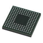
| 描述 | IC PROCESSOR DL 400MHZ 160CSPBGA数字信号处理器和控制器 - DSP, DSC 400MHz Hi Perf Gen Purp Blackfin |
| 产品分类 | |
| 品牌 | Analog Devices Inc |
| MIPS | 1200 MIPs |
| 产品手册 | |
| 产品图片 |
|
| rohs | 符合RoHS无铅 / 符合限制有害物质指令(RoHS)规范要求 |
| 产品系列 | 嵌入式处理器和控制器,数字信号处理器和控制器 - DSP, DSC,Analog Devices ADSP-BF533SBBCZ400Blackfin® |
| 数据手册 | |
| 产品型号 | ADSP-BF533SBBCZ400 |
| PCN设计/规格 | |
| 产品培训模块 | http://www.digikey.cn/PTM/IndividualPTM.page?site=cn&lang=zhs&ptm=12977http://www.digikey.cn/PTM/IndividualPTM.page?site=cn&lang=zhs&ptm=12972http://www.digikey.cn/PTM/IndividualPTM.page?site=cn&lang=zhs&ptm=12978http://www.digikey.cn/PTM/IndividualPTM.page?site=cn&lang=zhs&ptm=12970 |
| 产品种类 | 数字信号处理器和控制器 - DSP, DSC |
| 供应商器件封装 | 160-CSPBGA(12x12) |
| 其它名称 | ADSPBF533SBBCZ400 |
| 包装 | 托盘 |
| 可编程输入/输出端数量 | 16 |
| 商标 | Analog Devices |
| 商标名 | Blackfin |
| 安装类型 | 表面贴装 |
| 安装风格 | SMD/SMT |
| 定时器数量 | 4 |
| 封装 | Tray |
| 封装/外壳 | 160-LFBGA,CSPBGA |
| 封装/箱体 | BGA-160 |
| 工作温度 | -40°C ~ 85°C |
| 工作电源电压 | 1.8 V, 3.3 V |
| 工厂包装数量 | 189 |
| 接口 | SPI,SSP,UART |
| 数据RAM大小 | 64 kB |
| 数据总线宽度 | 16 bit |
| 时钟速率 | 400MHz |
| 最大工作温度 | + 85 C |
| 最大时钟频率 | 400 MHz |
| 最小工作温度 | - 40 C |
| 标准包装 | 1 |
| 核心 | Blackfin |
| 片载RAM | 148kB |
| 电压-I/O | 3.30V |
| 电压-内核 | 1.20V |
| 程序存储器大小 | 148 kB |
| 类型 | 定点 |
| 系列 | ADSP-BF533 |
| 输入/输出端数量 | 16 I/O |
| 配用 | /product-detail/zh/ADZS-BF533-EZLITE/ADZS-BF533-EZLITE-ND/612212/product-detail/zh/ADZS-BFAV-EZEXT/ADZS-BFAV-EZEXT-ND/857255/product-detail/zh/ADZS-BFAUDIO-EZEXT/ADZS-BFAUDIO-EZEXT-ND/1141753 |
| 非易失性存储器 | ROM(1 kB) |


- 商务部:美国ITC正式对集成电路等产品启动337调查
- 曝三星4nm工艺存在良率问题 高通将骁龙8 Gen1或转产台积电
- 太阳诱电将投资9.5亿元在常州建新厂生产MLCC 预计2023年完工
- 英特尔发布欧洲新工厂建设计划 深化IDM 2.0 战略
- 台积电先进制程称霸业界 有大客户加持明年业绩稳了
- 达到5530亿美元!SIA预计今年全球半导体销售额将创下新高
- 英特尔拟将自动驾驶子公司Mobileye上市 估值或超500亿美元
- 三星加码芯片和SET,合并消费电子和移动部门,撤换高东真等 CEO
- 三星电子宣布重大人事变动 还合并消费电子和移动部门
- 海关总署:前11个月进口集成电路产品价值2.52万亿元 增长14.8%

PDF Datasheet 数据手册内容提取
Blackfin Embedded Processor ADSP-BF531/ADSP-BF532/ADSP-BF533 FEATURES PERIPHERALS Up to 600MHz high performance Blackfin processor Parallel peripheral interface PPI, supporting Two 16-bit MACs, two 40-bit ALUs, four 8-bit video ALUs, ITU-R 656 video data formats 40-bit shifter 2 dual-channel, full duplex synchronous serial ports, sup- RISC-like register and instruction model for ease of pro- porting eight stereo I2S channels gramming and compiler-friendly support 2 memory-to-memory DMAs Advanced debug, trace, and performance monitoring 8 peripheral DMAs Wide range of operating voltages (see Operating Conditions SPI-compatible port on Page20) Three 32-bit timer/counters with PWM support Qualified for Automotive Applications (see Automotive Prod- Real-time clock and watchdog timer ucts on Page62) 32-bit core timer Programmable on-chip voltage regulator Up to 16 general-purpose I/O pins (GPIO) 160-ball CSP_BGA, 169-ball PBGA, and 176-lead LQFP UART with support for IrDA packages Event handler MEMORY Debug/JTAG interface On-chip PLL capable of frequency multiplication Up to 148Kbytes of on-chip memory (see Table1 on Page 3) Memory management unit providing memory protection External memory controller with glueless support for SDRAM, SRAM, flash, and ROM Flexible memory booting options from SPI and externalmemory VOLTAGEREGULATOR JTAGTESTANDEMULATION S B U B S INTERRUPT SEC WATCHDOG CONTROLLER CA TIMER L A R HE RTC P IR E L1 L1 P DMA PPI INSTRUCTION DATA CONTROLLER MEMORY MEMORY GPIO SU TIMER0-2 PORT B F DMA S DMACOREBUS EXTBEURSNAL CSEC SPI EXTERNALACCESSBUS A A EXTERNALPORT MD UART FLASH,SDRAMCONTROL SPORT0-1 16 BOOTROM Figure 1. Functional Block Diagram Blackfin and the Blackfin logo are registered trademarks of Analog Devices, Inc. Rev. I Document Feedback Information furnished by Analog Devices is believed to be accurate and reliable. However, no responsibility is assumed by Analog Devices for its use, nor for any infringements of patents or other rights of third parties that may result from its use. Specifications subject to change without notice. No license is granted by implication One Technology Way, P.O. Box 9106, Norwood, MA 02062-9106 U.S.A. or otherwise under any patent or patent rights of Analog Devices. Trademarks and Tel: 781.329.4700 ©2013 Analog Devices, Inc. All rights reserved. registered trademarks are the property of their respective owners. Technical Support www.analog.com
ADSP-BF531/ADSP-BF532/ADSP-BF533 TABLE OF CONTENTS Features ................................................................. 1 Development Tools .............................................. 15 Memory ................................................................ 1 Additional Information ........................................ 16 Peripherals ............................................................. 1 Related Signal Chains ........................................... 16 General Description ................................................. 3 Pin Descriptions .................................................... 17 Portable Low Power Architecture ............................. 3 Specifications ........................................................ 20 System Integration ................................................ 3 Operating Conditions ........................................... 20 Processor Peripherals ............................................. 3 Electrical Characteristics ....................................... 22 Blackfin Processor Core .......................................... 4 Absolute Maximum Ratings ................................... 25 Memory Architecture ............................................ 4 ESD Sensitivity ................................................... 25 DMA Controllers .................................................. 8 Package Information ............................................ 26 Real-Time Clock ................................................... 8 Timing Specifications ........................................... 27 Watchdog Timer .................................................. 9 Output Drive Currents ......................................... 43 Timers ............................................................... 9 Test Conditions .................................................. 45 Serial Ports (SPORTs) ............................................ 9 Thermal Characteristics ........................................ 49 Serial Peripheral Interface (SPI) Port ....................... 10 160-Ball CSP_BGA Ball Assignment ........................... 50 UART Port ........................................................ 10 169-Ball PBGA Ball Assignment ................................. 53 General-Purpose I/O Port F ................................... 10 176-Lead LQFP Pinout ............................................ 56 Parallel Peripheral Interface ................................... 11 Outline Dimensions ................................................ 58 Dynamic Power Management ................................ 11 Surface-Mount Design .......................................... 61 Voltage Regulation .............................................. 13 Automotive Products .............................................. 62 Clock Signals ..................................................... 13 Ordering Guide ..................................................... 63 Booting Modes ................................................... 14 Instruction Set Description ................................... 15 REVISION HISTORY 8/13— Rev. H to Rev. I Updated Development Tools .................................... 15 Corrected Conditions value of the V specification in IL Operating Conditions ............................................. 20 Added notes to Table 30 in Serial Ports—Enable and Three-State .......................... 36 Added Timer Clock Timing ...................................... 41 Revised Timer Cycle Timing ..................................... 41 Updated Ordering Guide ......................................... 63 Rev. I | Page 2 of 64 | August 2013
ADSP-BF531/ADSP-BF532/ADSP-BF533 GENERAL DESCRIPTION The ADSP-BF531/ADSP-BF532/ADSP-BF533 processors are PORTABLE LOW POWER ARCHITECTURE members of the Blackfin® family of products, incorporating the Blackfin processors provide world-class power management Analog Devices, Inc./Intel Micro Signal Architecture (MSA). and performance. Blackfin processors are designed in a low Blackfin processors combine a dual-MAC state-of-the-art signal power and low voltage design methodology and feature processing engine, the advantages of a clean, orthogonal RISC- dynamic power management—the ability to vary both the volt- like microprocessor instruction set, and single instruction, mul- age and frequency of operation to significantly lower overall tiple data (SIMD) multimedia capabilities into a single power consumption. Varying the voltage and frequency can instruction set architecture. result in a substantial reduction in power consumption, com- The ADSP-BF531/ADSP-BF532/ADSP-BF533 processors are pared with just varying the frequency of operation. This completely code and pin-compatible, differing only with respect translates into longer battery life for portable appliances. to their performance and on-chip memory. Specific perfor- mance and memory configurations are shown in Table1. SYSTEM INTEGRATION The ADSP-BF531/ADSP-BF532/ADSP-BF533 processors are Table 1. Processor Comparison highly integrated system-on-a-chip solutions for the next gener- 1 2 3 ation of digital communication and consumer multimedia 3 3 3 5 5 5 applications. By combining industry-standard interfaces with a F F F B B B high performance signal processing core, users can develop P- P- P- S S S cost-effective solutions quickly without the need for costly Features D D D A A A external components. The system peripherals include a UART SPORTs 2 2 2 port, an SPI port, two serial ports (SPORTs), four general-pur- pose timers (three with PWM capability), a real-time clock, a UART 1 1 1 watchdog timer, and a parallel peripheral interface. SPI 1 1 1 PROCESSOR PERIPHERALS GP Timers 3 3 3 Watchdog Timers 1 1 1 The ADSP-BF531/ADSP-BF532/ADSP-BF533 processors con- RTC 1 1 1 tain a rich set of peripherals connected to the core via several high bandwidth buses, providing flexibility in system configura- Parallel Peripheral Interface 1 1 1 tion as well as excellent overall system performance (see the GPIOs 16 16 16 functional block diagram in Figure1 on Page1). The general- on L1 Instruction SRAM/Cache 16K bytes 16K bytes 16K bytes purpose peripherals include functions such as UART, timers ti a L1 Instruction SRAM 16K bytes 32K bytes 64K bytes with PWM (pulse-width modulation) and pulse measurement ur g L1 Data SRAM/Cache 16K bytes 32K bytes 32K bytes capability, general-purpose I/O pins, a real-time clock, and a nfi watchdog timer. This set of functions satisfies a wide variety of o L1 Data SRAM 32K bytes y C L1 Scratchpad 4K bytes 4K bytes 4K bytes typical system support needs and is augmented by the system or expansion capabilities of the part. In addition to these general- em L3 Boot ROM 1K bytes 1K bytes 1K bytes purpose peripherals, the processors contain high speed serial M and parallel ports for interfacing to a variety of audio, video, and Maximum Speed Grade 400 MHz 400 MHz 600 MHz modem codec functions; an interrupt controller for flexible Package Options: management of interrupts from the on-chip peripherals or CSP_BGA 160-Ball 160-Ball 160-Ball external sources; and power management control functions to Plastic BGA 169-Ball 169-Ball 169-Ball tailor the performance and power characteristics of the proces- LQFP 176-Lead 176-Lead 176-Lead sor and system to many application scenarios. All of the peripherals, except for general-purpose I/O, real-time By integrating a rich set of industry-leading system peripherals clock, and timers, are supported by a flexible DMA structure. and memory, Blackfin processors are the platform of choice for There is also a separate memory DMA channel dedicated to next generation applications that require RISC-like program- data transfers between the processor’s various memory spaces, mability, multimedia support, and leading-edge signal including external SDRAM and asynchronous memory. Multi- processing in one integrated package. ple on-chip buses running at up to 133MHz provide enough bandwidth to keep the processor core running along with activ- ity on all of the on-chip and external peripherals. The processors include an on-chip voltage regulator in support of the processor’s dynamic power management capability. The voltage regulator provides a range of core voltage levels from V . The voltage regulator can be bypassed at the user’s DDEXT discretion. Rev. I | Page 3 of 64 | August 2013
ADSP-BF531/ADSP-BF532/ADSP-BF533 BLACKFIN PROCESSOR CORE In addition, multiple L1 memory blocks are provided, offering a configurable mix of SRAM and cache. The memory manage- As shown in Figure2 on Page5, the Blackfin processor core ment unit (MMU) provides memory protection for individual contains two 16-bit multipliers, two 40-bit accumulators, two tasks that may be operating on the core and can protect system 40-bit ALUs, four video ALUs, and a 40-bit shifter. The compu- registers from unintended access. tation units process 8-bit, 16-bit, or 32-bit data from the registerfile. The architecture provides three modes of operation: user mode, supervisor mode, and emulation mode. User mode has The compute register file contains eight 32-bit registers. When restricted access to certain system resources, thus providing a performing compute operations on 16-bit operand data, the protected software environment, while supervisor mode has register file operates as 16 independent 16-bit registers. All unrestricted access to the system and core resources. operands for compute operations come from the multiported register file and instruction constant fields. The Blackfin processor instruction set has been optimized so that 16-bit opcodes represent the most frequently used instruc- Each MAC can perform a 16-bit by 16-bit multiply in each tions, resulting in excellent compiled code density. Complex cycle, accumulating the results into the 40-bit accumulators. DSP instructions are encoded into 32-bit opcodes, representing Signed and unsigned formats, rounding, and saturation are fully featured multifunction instructions. Blackfin processors supported. support a limited multi-issue capability, where a 32-bit instruc- The ALUs perform a traditional set of arithmetic and logical tion can be issued in parallel with two 16-bit instructions, operations on 16-bit or 32-bit data. In addition, many special allowing the programmer to use many of the core resources in a instructions are included to accelerate various signal processing single instruction cycle. tasks. These include bit operations such as field extract and The Blackfin processor assembly language uses an algebraic syn- population count, modulo 232 multiply, divide primitives, satu- tax for ease of coding and readability. The architecture has been ration and rounding, and sign/exponent detection. The set of optimized for use in conjunction with the C/C++compiler, video instructions includes byte alignment and packing opera- resulting in fast and efficient software implementations. tions, 16-bit and 8-bit adds with clipping, 8-bit average operations, and 8-bit subtract/absolute value/accumulate (SAA) MEMORY ARCHITECTURE operations. Also provided are the compare/select and vector The ADSP-BF531/ADSP-BF532/ADSP-BF533 processors view search instructions. memory as a single unified 4Gbyte address space, using 32-bit For certain instructions, two 16-bit ALU operations can be per- addresses. All resources, including internal memory, external formed simultaneously on register pairs (a 16-bit high half and memory, and I/O control registers, occupy separate sections of 16-bit low half of a compute register). Quad 16-bit operations this common address space. The memory portions of this are possible using the second ALU. address space are arranged in a hierarchical structure to provide The 40-bit shifter can perform shifts and rotates and is used to a good cost/performance balance of some very fast, low latency support normalization, field extract, and field deposit on-chip memory as cache or SRAM, and larger, lower cost and instructions. performance off-chip memory systems. See Figure3, Figure4, and Figure5 on Page6. The program sequencer controls the flow of instruction execu- tion, including instruction alignment and decoding. For The L1 memory system is the primary highest performance program flow control, the sequencer supports PC relative and memory available to the Blackfin processor. The off-chip mem- indirect conditional jumps (with static branch prediction), and ory system, accessed through the external bus interface unit subroutine calls. Hardware is provided to support zero-over- (EBIU), provides expansion with SDRAM, flash memory, and head looping. The architecture is fully interlocked, meaning that SRAM, optionally accessing up to 132Mbytes of the programmer need not manage the pipeline when executing physicalmemory. instructions with data dependencies. The memory DMA controller provides high bandwidth data- The address arithmetic unit provides two addresses for simulta- movement capability. It can perform block transfers of code or neous dual fetches from memory. It contains a multiported data between the internal memory and the external register file consisting of four sets of 32-bit index, modify, memoryspaces. length, and base registers (for circular buffering), and eight Internal (On-Chip) Memory additional 32-bit pointer registers (for C-style indexed stack manipulation). The processors have three blocks of on-chip memory that pro- vide high bandwidth access to the core. Blackfin processors support a modified Harvard architecture in combination with a hierarchical memory structure. Level 1 (L1) The first block is the L1 instruction memory, consisting of up to memories are those that typically operate at the full processor 80Kbytes SRAM, of which 16Kbytes can be configured as a speed with little or no latency. At the L1 level, the instruction four way set-associative cache. This memory is accessed at full memory holds instructions only. The two data memories hold processor speed. data, and a dedicated scratchpad data memory stores stack and local variable information. Rev. I | Page 4 of 64 | August 2013
ADSP-BF531/ADSP-BF532/ADSP-BF533 ADDRESS ARITHMETIC UNIT SP I3 L3 B3 M3 FP I2 L2 B2 M2 P5 I1 L1 B1 M1 DAG1 P4 I0 L0 B0 M0 P3 DAG0 P2 DA1 32 P1 DA0 32 P0 RY 32 32 MO RAB PREG E M O T SD 32 LD1 32 32 ASTAT LD0 32 32 SEQUENCER R7.H R7.L R6.H R6.L R5.H R5.L 16 16 ALIGN R4.H R4.L 8 8 8 8 R3.H R3.L R2.H R2.L DECODE R1.H R1.L BARREL R0.H R0.L SHIFTER 40 40 LOOP BUFFER 40 40 A0 A1 CONTROL UNIT 32 32 DATA ARITHMETIC UNIT Figure 2. Blackfin Processor Core The second on-chip memory block is the L1 data memory, con- 1Mbyte segment regardless of the size of the devices used, so sisting of one or two banks of up to 32Kbytes. The memory that these banks are only contiguous if each is fully populated banks are configurable, offering both cache and SRAM func- with 1Mbyte of memory. tionality. This memory block is accessed at full processor speed. I/O Memory Space The third memory block is a 4Kbyte scratchpad SRAM, which runs at the same speed as the L1 memories, but is only accessible Blackfin processors do not define a separate I/O space. All as data SRAM and cannot be configured as cache memory. resources are mapped through the flat 32-bit address space. On-chip I/O devices have their control registers mapped into External (Off-Chip) Memory memory mapped registers (MMRs) at addresses near the top of the 4Gbyte address space. These are separated into two smaller External memory is accessed via the external bus interface unit blocks, one containing the control MMRs for all core functions, (EBIU). This 16-bit interface provides a glueless connection to a and the other containing the registers needed for setup and con- bank of synchronous DRAM (SDRAM) as well as up to four trol of the on-chip peripherals outside of the core. The MMRs banks of asynchronous memory devices including flash, are accessible only in supervisor mode and appear as reserved EPROM, ROM, SRAM, and memory mapped I/O devices. space to on-chip peripherals. The PC133-compliant SDRAM controller can be programmed to interface to up to 128Mbytes of SDRAM. The SDRAM con- Booting troller allows one row to be open for each internal SDRAM The ADSP-BF531/ADSP-BF532/ADSP-BF533 processors con- bank, for up to four internal SDRAM banks, improving overall tain a small boot kernel, which configures the appropriate system performance. peripheral for booting. If the processors are configured to boot The asynchronous memory controller can be programmed to from boot ROM memory space, the processor starts executing control up to four banks of devices with very flexible timing from the on-chip boot ROM. For more information, see Boot- parameters for a wide variety of devices. Each bank occupies a ing Modes on Page14. Rev. I | Page 5 of 64 | August 2013
ADSP-BF531/ADSP-BF532/ADSP-BF533 0xFFFFFFFF 0xFFFFFFFF COREMMRREGISTERS(2MBYTE) COREMMRREGISTERS(2MBYTE) 0xFFE00000 0xFFE00000 SYSTEMMMRREGISTERS(2MBYTE) SYSTEMMMRREGISTERS(2MBYTE) 0xFFC00000 0xFFC00000 RESERVED RESERVED 0xFFB01000 0xFFB01000 SCRATCHPADSRAM(4KBYTE) SCRATCHPADSRAM(4KBYTE) 0xFFB00000 0xFFB00000 RESERVED RESERVED AP 0xFFA14000 P 0xFFA14000 M INSTRUCTIONSRAM/CACHE(16KBYTE) A INSTRUCTIONSRAM/CACHE(16KBYTE) Y 0xFFA10000 YM 0xFFA10000 OR RESERVED R INSTRUCTIONSRAM(64KBYTE) M 0xFFA0C000 MO 0xFFA00000 ME INSTRUCTIONSRAM(16KBYTE) E RESERVED L 0xFFA08000 M 0xFF908000 A RESERVED AL DATABANKBSRAM/CACHE(16KBYTE) RN 00xxFFFFA90080000000 RESERVED NTERN 00xxFFFF990040000000 DATABANKBSRAM(16KBYTE) ITNE RESERVED I RESERVED 0xFF904000 0xFF808000 RESERVED DATABANKASRAM/CACHE(16KBYTE) 0xFF808000 0xFF804000 DATABANKASRAM/CACHE(16KBYTE) DATABANKASRAM(16KBYTE) 0xFF804000 0xFF800000 RESERVED RESERVED 0xEF000000 0xEF000000 RESERVED RESERVED 0x20400000 AP 0x20400000 AP ASYNCMEMORYBANK3(1MBYTE) M ASYNCMEMORYBANK3(1MBYTE) M 0x20300000 ASYNCMEMORYBANK2(1MBYTE) ORY 0x20300000 ASYNCMEMORYBANK2(1MBYTE) YOR 0x20200000 M 0x20200000 M ASYNCMEMORYBANK1(1MBYTE) ME ASYNCMEMORYBANK1(1MBYTE) ME 0x20100000 ASYNCMEMORYBANK0(1MBYTE) ALN 0x20100000 ASYNCMEMORYBANK0(1MBYTE) NAL 0x20000000 R 0x20000000 R 0x08000000 RESERVED EXTE 0x08000000 RESERVED EXTE SDRAMMEMORY(16MBYTETO128MBYTE) SDRAMMEMORY(16MBYTETO128MBYTE) 0x00000000 0x00000000 Figure 3. ADSP-BF531 Internal/External Memory Map Figure 5. ADSP-BF533 Internal/External Memory Map Event Handling 0xFFFFFFFF COREMMRREGISTERS(2MBYTE) The event controller on the processors handle all asynchronous 0xFFE00000 SYSTEMMMRREGISTERS(2MBYTE) and synchronous events to the processor. The ADSP-BF531/ 0xFFC00000 ADSP-BF532/ADSP-BF533 processors provide event handling RESERVED 0xFFB01000 that supports both nesting and prioritization. Nesting allows SCRATCHPADSRAM(4KBYTE) 0xFFB00000 P multiple event service routines to be active simultaneously. Pri- RESERVED AM oritization ensures that servicing of a higher priority event takes 0xFFA14000 Y INSTRUCTIONSRAM/CACHE(16KBYTE) R precedence over servicing of a lower priority event. The control- 0xFFA10000 MO ler provides support for five different types of events: INSTRUCTIONSRAM(32KBYTE) E 0xFFA08000 M RESERVED AL • Emulation – An emulation event causes the processor to 0xFFA00000 RN enter emulation mode, allowing command and control of RESERVED E 0xFF908000 NT the processor via the JTAG interface. DATABANKBSRAM/CACHE(16KBYTE) I 0xFF904000 • Reset – This event resets the processor. RESERVED 0xFF808000 • Nonmaskable Interrupt (NMI) – The NMI event can be DATABANKASRAM/CACHE(16KBYTE) 0xFF804000 generated by the software watchdog timer or by the NMI RESERVED input signal to the processor. The NMI event is frequently 0xEF000000 RESERVED used as a power-down indicator to initiate an orderly shut- 0x20400000 ASYNCMEMORYBANK3(1MBYTE) APM down of the system. 0x20300000 Y ASYNCMEMORYBANK2(1MBYTE) RO • Exceptions – Events that occur synchronously to program 0x20200000 EM flow (i.e., the exception is taken before the instruction is ASYNCMEMORYBANK1(1MBYTE) M 0x20100000 L allowed to complete). Conditions such as data alignment 0x20000000 ASYNCMEMORYBANK0(1MBYTE) RNA violations and undefined instructions cause exceptions. E RESERVED T 0x08000000 EX • Interrupts – Events that occur asynchronously to program SDRAMMEMORY(16MBYTETO128MBYTE) flow. They are caused by input pins, timers, and other 0x00000000 peripherals, as well as by an explicit software instruction. Figure 4. ADSP-BF532 Internal/External Memory Map Rev. I | Page 6 of 64 | August 2013
ADSP-BF531/ADSP-BF532/ADSP-BF533 Each event type has an associated register to hold the return Table 3. System Interrupt Controller (SIC) address and an associated return-from-event instruction. When an event is triggered, the state of the processor is saved on the Peripheral Interrupt Event Default Mapping supervisor stack. PLL Wakeup IVG7 The ADSP-BF531/ADSP-BF532/ADSP-BF533 processors’ event DMA Error IVG7 controller consists of two stages, the core event controller (CEC) PPI Error IVG7 and the system interrupt controller (SIC). The core event con- SPORT 0 Error IVG7 troller works with the system interrupt controller to prioritize SPORT 1 Error IVG7 and control all system events. Conceptually, interrupts from the SPI Error IVG7 peripherals enter into the SIC, and are then routed directly into the general-purpose interrupts of the CEC. UART Error IVG7 Real-Time Clock IVG8 Core Event Controller (CEC) DMA Channel 0 (PPI) IVG8 The CEC supports nine general-purpose interrupts (IVG15–7), DMA Channel 1 (SPORT 0 Receive) IVG9 in addition to the dedicated interrupt and exception events. Of DMA Channel 2 (SPORT 0 Transmit) IVG9 these general-purpose interrupts, the two lowest priority inter- rupts (IVG15–14) are recommended to be reserved for software DMA Channel 3 (SPORT 1 Receive) IVG9 interrupt handlers, leaving seven prioritized interrupt inputs to DMA Channel 4 (SPORT 1 Transmit) IVG9 support the peripherals of the processor. Table2 describes the DMA Channel 5 (SPI) IVG10 inputs to the CEC, identifies their names in the event vector DMA Channel 6 (UART Receive) IVG10 table (EVT), and lists their priorities. DMA Channel 7 (UART Transmit) IVG10 Table 2. Core Event Controller (CEC) Timer 0 IVG11 Timer 1 IVG11 Priority Timer 2 IVG11 (0 is Highest) Event Class EVT Entry Port F GPIO Interrupt A IVG12 0 Emulation/Test Control EMU Port F GPIO Interrupt B IVG12 1 Reset RST Memory DMA Stream 0 IVG13 2 Nonmaskable Interrupt NMI Memory DMA Stream 1 IVG13 3 Exception EVX Software Watchdog Timer IVG13 4 Reserved 5 Hardware Error IVHW Event Control 6 Core Timer IVTMR The processors provide a very flexible mechanism to control the 7 General Interrupt 7 IVG7 processing of events. In the CEC, three registers are used to 8 General Interrupt 8 IVG8 coordinate and control events. Each register is 32 bits wide: 9 General Interrupt 9 IVG9 • CEC interrupt latch register (ILAT) – The ILAT register 10 General Interrupt 10 IVG10 indicates when events have been latched. The appropriate 11 General Interrupt 11 IVG11 bit is set when the processor has latched the event and cleared when the event has been accepted into the system. 12 General Interrupt 12 IVG12 This register is updated automatically by the controller, but 13 General Interrupt 13 IVG13 it can also be written to clear (cancel) latched events. This 14 General Interrupt 14 IVG14 register can be read while in supervisor mode and can only 15 General Interrupt 15 IVG15 be written while in supervisor mode when the correspond- ing IMASK bit is cleared. System Interrupt Controller (SIC) • CEC interrupt mask register (IMASK) – The IMASK regis- The system interrupt controller provides the mapping and rout- ter controls the masking and unmasking of individual ing of events from the many peripheral interrupt sources to the events. When a bit is set in the IMASK register, that event is prioritized general-purpose interrupt inputs of the CEC. unmasked and is processed by the CEC when asserted. A Although the processors provide a default mapping, the user cleared bit in the IMASK register masks the event, can alter the mappings and priorities of interrupt events by writ- preventing the processor from servicing the event even ing the appropriate values into the interrupt assignment though the event may be latched in the ILAT register. This registers (SIC_IARx). Table3 describes the inputs into the SIC register can be read or written while in supervisor mode. and the default mappings into the CEC. Note that general-purpose interrupts can be globally enabled and disabled with the STI and CLI instructions, respectively. Rev. I | Page 7 of 64 | August 2013
ADSP-BF531/ADSP-BF532/ADSP-BF533 • CEC interrupt pending register (IPEND) – The IPEND peripherals include the SPORTs, SPI port, UART, and PPI. Each register keeps track of all nested events. A set bit in the individual DMA-capable peripheral has at least one dedicated IPEND register indicates the event is currently active or DMA channel. nested at some level. This register is updated automatically The DMA controller supports both 1-dimensional (1-D) and 2- by the controller but can be read while in supervisor mode. dimensional (2-D) DMA transfers. DMA transfer initialization The SIC allows further control of event processing by providing can be implemented from registers or from sets of parameters three 32-bit interrupt control and status registers. Each register called descriptor blocks. contains a bit corresponding to each of the peripheral interrupt The 2-D DMA capability supports arbitrary row and column events shown in Table3. sizes up to 64K elements by 64K elements, and arbitrary row • SIC interrupt mask register (SIC_IMASK) – This register and column step sizes up to ±32K elements. Furthermore, the controls the masking and unmasking of each peripheral column step size can be less than the row step size, allowing interrupt event. When a bit is set in this register, that implementation of interleaved data streams. This feature is peripheral event is unmasked and is processed by the sys- especially useful in video applications where data can be tem when asserted. A cleared bit in this register masks the de-interleaved on the fly. peripheral event, preventing the processor from servicing Examples of DMA types supported by the DMA controller the event. include: • SIC interrupt status register (SIC_ISR) – As multiple • A single, linear buffer that stops upon completion peripherals can be mapped to a single event, this register allows the software to determine which peripheral event • A circular, autorefreshing buffer that interrupts on each source triggered the interrupt. A set bit indicates the full or fractionally full buffer peripheral is asserting the interrupt, and a cleared bit indi- • 1-D or 2-D DMA using a linked list of descriptors cates the peripheral is not asserting the event. • 2-D DMA using an array of descriptors, specifying only the • SIC interrupt wakeup enable register (SIC_IWR) – By base DMA address within a common page enabling the corresponding bit in this register, a peripheral In addition to the dedicated peripheral DMA channels, there are can be configured to wake up the processor, should the two pairs of memory DMA channels provided for transfers core be idled when the event is generated. See Dynamic between the various memories of the processor system. This Power Management on Page11. enables transfers of blocks of data between any of the memo- Because multiple interrupt sources can map to a single general- ries—including external SDRAM, ROM, SRAM, and flash purpose interrupt, multiple pulse assertions can occur simulta- memory—with minimal processor intervention. Memory DMA neously, before or during interrupt processing for an interrupt transfers can be controlled by a very flexible descriptor-based event already detected on this interrupt input. The IPEND reg- methodology or by a standard register-based autobuffer ister contents are monitored by the SIC as the interrupt mechanism. acknowledgement. REAL-TIME CLOCK The appropriate ILAT register bit is set when an interrupt rising edge is detected (detection requires two core clock cycles). The The processor real-time clock (RTC) provides a robust set of bit is cleared when the respective IPEND register bit is set. The digital watch features, including current time, stopwatch, and IPEND bit indicates that the event has entered into the proces- alarm. The RTC is clocked by a 32.768kHz crystal external to sor pipeline. At this point the CEC recognizes and queues the the ADSP-BF531/ADSP-BF532/ADSP-BF533 processors. The next rising edge event on the corresponding event input. The RTC peripheral has dedicated power supply pins so that it can minimum latency from the rising edge transition of the remain powered up and clocked even when the rest of the pro- general-purpose interrupt to the IPEND output asserted is three cessor is in a low power state. The RTC provides several core clock cycles; however, the latency can be much higher, programmable interrupt options, including interrupt per sec- depending on the activity within and the state of the processor. ond, minute, hour, or day clock ticks, interrupt on programmable stopwatch countdown, or interrupt at a pro- DMA CONTROLLERS grammed alarm time. The ADSP-BF531/ADSP-BF532/ADSP-BF533 processors have The 32.768kHz input clock frequency is divided down to a 1Hz multiple, independent DMA channels that support automated signal by a prescaler. The counter function of the timer consists data transfers with minimal overhead for the processor core. of four counters: a 60 second counter, a 60 minute counter, a DMA transfers can occur between the processor’s internal 24hour counter, and a 32,768 day counter. memories and any of its DMA-capable peripherals. Addition- When enabled, the alarm function generates an interrupt when ally, DMA transfers can be accomplished between any of the the output of the timer matches the programmed value in the DMA-capable peripherals and external devices connected to the alarm control register. The two alarms are time of day and a day external memory interfaces, including the SDRAM controller and time of that day. and the asynchronous memory controller. DMA-capable Rev. I | Page 8 of 64 | August 2013
ADSP-BF531/ADSP-BF532/ADSP-BF533 The stopwatch function counts down from a programmed TIMERS value, with one second resolution. When the stopwatch is There are four general-purpose programmable timer units in enabled and the counter underflows, an interrupt is generated. the ADSP-BF531/ADSP-BF532/ADSP-BF533 processors. Three Like other peripherals, the RTC can wake up the processor from timers have an external pin that can be configured either as a sleep mode upon generation of any RTC wakeup event. pulse-width modulator (PWM) or timer output, as an input to Additionally, an RTC wakeup event can wake up the processor clock the timer, or as a mechanism for measuring pulse widths from deep sleep mode, and wake up the on-chip internal voltage and periods of external events. These timers can be synchro- regulator from a powered-down state. nized to an external clock input to the PF1 pin (TACLK), an Connect RTC pins RTXI and RTXO with external components external clock input to the PPI_CLK pin (TMRCLK), or to the as shown in Figure6. internal SCLK. The timer units can be used in conjunction with the UART to RTXI RTXO measure the width of the pulses in the data stream to provide an autobaud detect function for a serial channel. R1 The timers can generate interrupts to the processor core provid- ing periodic events for synchronization, either to the system X1 clock or to a count of external signals. C1 C2 In addition to the three general-purpose programmable timers, a fourth timer is also provided. This extra timer is clocked by the internal processor clock and is typically used as a system tick clock for generation of operating system periodic interrupts. SUGGESTEDCOMPONENTS: X1=ECLIPTEKEC38J(THROUGH-HOLEPACKAGE)OR SERIAL PORTS (SPORTs) EPSONMC40512pFLOAD(SURFACE-MOUNTPACKAGE) C1=22pF The ADSP-BF531/ADSP-BF532/ADSP-BF533 processors C2=22pF R1=10M(cid:58) incorporate two dual-channel synchronous serial ports NOTE:C1ANDC2ARESPECIFICTOCRYSTALSPECIFIEDFORX1. (SPORT0 and SPORT1) for serial and multiprocessor commu- CONTACTCRYSTALMANUFACTURERFORDETAILS.C1ANDC2 nications. The SPORTs support the following features: SPECIFICATIONSASSUMEBOARDTRACECAPACITANCEOF3pF. • I2S capable operation. Figure 6. External Components for RTC • Bidirectional operation – Each SPORT has two sets of inde- WATCHDOG TIMER pendent transmit and receive pins, enabling eight channels of I2S stereo audio. The ADSP-BF531/ADSP-BF532/ADSP-BF533 processors include a 32-bit timer that can be used to implement a software • Buffered (8-deep) transmit and receive ports – Each port watchdog function. A software watchdog can improve system has a data register for transferring data words to and from availability by forcing the processor to a known state through other processor components and shift registers for shifting generation of a hardware reset, nonmaskable interrupt (NMI), data in and out of the data registers. or general-purpose interrupt, if the timer expires before being • Clocking – Each transmit and receive port can either use an reset by software. The programmer initializes the count value of external serial clock or generate its own, in frequencies the timer, enables the appropriate interrupt, then enables the ranging from (f /131,070)Hz to (f /2)Hz. SCLK SCLK timer. Thereafter, the software must reload the counter before it • Word length – Each SPORT supports serial data words counts to zero from the programmed value. This protects the from 3 bits to 32bits in length, transferred most-signifi- system from remaining in an unknown state where software, cant-bit first or least-significant-bit first. which would normally reset the timer, has stopped running due to an external noise condition or software error. • Framing – Each transmit and receive port can run with or without frame sync signals for each data word. Frame sync If configured to generate a hardware reset, the watchdog timer signals can be generated internally or externally, active high resets both the core and the processor peripherals. After a reset, or low, and with either of two pulse widths and early or late software can determine if the watchdog was the source of the frame sync. hardware reset by interrogating a status bit in the watchdog timer control register. • Companding in hardware – Each SPORT can perform A-law or μ-law companding according to ITU recommen- The timer is clocked by the system clock (SCLK), at a maximum dation G.711. Companding can be selected on the transmit frequency of f . SCLK and/or receive channel of the SPORT without additional latencies. • DMA operations with single-cycle overhead – Each SPORT can automatically receive and transmit multiple buffers of memory data. The processor can link or chain sequences of DMA transfers between a SPORT and memory. Rev. I | Page 9 of 64 | August 2013
ADSP-BF531/ADSP-BF532/ADSP-BF533 • Interrupts – Each transmit and receive port generates an • DMA (direct memory access) – The DMA controller trans- interrupt upon completing the transfer of a data-word or fers both transmit and receive data. This reduces the after transferring an entire data buffer or buffers number and frequency of interrupts required to transfer throughDMA. data to and from memory. The UART has two dedicated DMA channels, one for transmit and one for receive. These • Multichannel capability – Each SPORT supports 128 chan- DMA channels have lower default priority than most DMA nels out of a 1,024-channel window and is compatible with channels because of their relatively low service rates. the H.100, H.110, MVIP-90, and HMVIP standards. The baud rate, serial data format, error code generation and sta- An additional 250 mV of SPORT input hysteresis can be tus, and interrupts for the UART port are programmable. enabled by setting Bit 15 of the PLL_CTL register. When this bit is set, all SPORT input pins have the increased hysteresis. The UART programmable features include: SERIAL PERIPHERAL INTERFACE (SPI) PORT • Supporting bit rates ranging from (fSCLK/1,048,576) bits per second to (f /16) bits per second. SCLK The ADSP-BF531/ADSP-BF532/ADSP-BF533 processors have • Supporting data formats from seven bits to 12bits per an SPI-compatible port that enables the processor to communi- frame. cate with multiple SPI-compatible devices. • Both transmit and receive operations can be configured to The SPI interface uses three pins for transferring data: two data generate maskable interrupts to the processor. pins (master output-slave input, MOSI, and master input-slave output, MISO) and a clock pin (serial clock, SCK). An SPI chip The UART port’s clock rate is calculated as: select input pin (SPISS) lets other SPI devices select the proces- f UART Clock Rate = ---------------------S--C--L---K------------------- sor, and seven SPI chip select output pins (SPISEL7–1) let the 16UART_Divisor processor select other SPI devices. The SPI select pins are recon- where the 16-bit UART_Divisor comes from the UART_DLH figured general-purpose I/O pins. Using these pins, the SPI port register (most significant 8 bits) and UART_DLL register (least provides a full-duplex, synchronous serial interface which sup- significant 8bits). ports both master/slave modes and multimaster environments. In conjunction with the general-purpose timer functions, The baud rate and clock phase/polarities for the SPI port are autobaud detection is supported. programmable, and it has an integrated DMA controller, con- figurable to support transmit or receive data streams. The SPI The capabilities of the UART are further extended with support DMA controller can only service unidirectional accesses at any for the Infrared Data Association (IrDA®) serial infrared physi- given time. cal layer link specification (SIR) protocol. The SPI port clock rate is calculated as: GENERAL-PURPOSE I/O PORT F f The ADSP-BF531/ADSP-BF532/ADSP-BF533 processors have SPI Clock Rate = ---------------S--C---L--K-------------- 2SPI_BAUD 16 bidirectional, general-purpose I/O pins on Port F (PF15–0). Each general-purpose I/O pin can be individually controlled by where the 16-bit SPI_BAUD register contains a value of 2 to manipulation of the GPIO control, status and interrupt 65,535. registers: During transfers, the SPI port simultaneously transmits and • GPIO direction control register – Specifies the direction of receives by serially shifting data in and out on its two serial data each individual PFx pin as input or output. lines. The serial clock line synchronizes the shifting and sam- • GPIO control and status registers – The processor employs pling of data on the two serial data lines. a “write one to modify” mechanism that allows any combi- UART PORT nation of individual GPIO pins to be modified in a single instruction, without affecting the level of any other GPIO The ADSP-BF531/ADSP-BF532/ADSP-BF533 processors pro- pins. Four control registers are provided. One register is vide a full-duplex universal asynchronous receiver/transmitter written in order to set GPIO pin values, one register is writ- (UART) port, which is fully compatible with PC-standard ten in order to clear GPIO pin values, one register is written UARTs. The UART port provides a simplified UART interface in order to toggle GPIO pin values, and one register is writ- to other peripherals or hosts, supporting full-duplex, DMA-sup- ten in order to specify GPIO pin values. Reading the GPIO ported, asynchronous transfers of serial data. The UART port status register allows software to interrogate the sense of includes support for 5 data bits to 8data bits, 1 stop bit or 2stop the GPIO pin. bits, and none, even, or odd parity. The UART port supports • GPIO interrupt mask registers – The two GPIO interrupt two modes of operation: mask registers allow each individual PFx pin to function as • PIO (programmed I/O) – The processor sends or receives an interrupt to the processor. Similar to the two GPIO data by writing or reading I/O-mapped UART registers. control registers that are used to set and clear individual The data is double-buffered on both transmit and receive. GPIO pin values, one GPIO interrupt mask register sets bits to enable interrupt function, and the other GPIO inter- rupt mask register clears bits to disable interrupt function. Rev. I | Page 10 of 64 | August 2013
ADSP-BF531/ADSP-BF532/ADSP-BF533 PFx pins defined as inputs can be configured to generate Output Mode hardware interrupts, while output PFx pins can be trig- Output mode is used for transmitting video or other data with gered by software interrupts. up to three output frame syncs. Typically, a single frame sync is • GPIO interrupt sensitivity registers – The two GPIO inter- appropriate for data converter applications, whereas two or rupt sensitivity registers specify whether individual PFx three frame syncs could be used for sending video with hard- pins are level- or edge-sensitive and specify—if edge-sensi- ware signaling. tive—whether just the rising edge or both the rising and ITU-R 656 Mode Descriptions falling edges of the signal are significant. One register selects the type of sensitivity, and one register selects which The ITU-R 656 modes of the PPI are intended to suit a wide edges are significant for edge-sensitivity. variety of video capture, processing, and transmission applica- tions. Three distinct sub modes are supported: PARALLEL PERIPHERAL INTERFACE • Active video only mode The processors provide a parallel peripheral interface (PPI) that • Vertical blanking only mode can connect directly to parallel ADCs and DACs, video encod- ers and decoders, and other general-purpose peripherals. The • Entire field mode PPI consists of a dedicated input clock pin, up to three frame Active Video Only Mode synchronization pins, and up to 16 data pins. The input clock supports parallel data rates up to half the system clock rate and Active video only mode is used when only the active video por- the synchronization signals can be configured as either inputs or tion of a field is of interest and not any of the blanking intervals. outputs. The PPI does not read in any data between the end of active video (EAV) and start of active video (SAV) preamble symbols, The PPI supports a variety of general-purpose and ITU-R 656 or any data present during the vertical blanking intervals. In this modes of operation. In general-purpose mode, the PPI provides mode, the control byte sequences are not stored to memory; half-duplex, bi-directional data transfer with up to 16 bits of they are filtered by the PPI. After synchronizing to the start of data. Up to three frame synchronization signals are also pro- Field 1, the PPI ignores incoming samples until it sees an SAV vided. In ITU-R 656 mode, the PPI provides half-duplex bi- code. The user specifies the number of active video lines per directional transfer of 8- or 10-bit video data. Additionally, on- frame (in PPI_COUNT register). chip decode of embedded start-of-line (SOL) and start-of-field (SOF) preamble packets is supported. Vertical Blanking Interval Mode General-Purpose Mode Descriptions In this mode, the PPI only transfers vertical blanking interval (VBI) data. The general-purpose modes of the PPI are intended to suit a wide variety of data capture and transmission applications. Entire Field Mode Three distinct sub modes are supported: In this mode, the entire incoming bit stream is read in through • Input mode – Frame syncs and data are inputs into the PPI. the PPI. This includes active video, control preamble sequences, and ancillary data that can be embedded in horizontal and verti- • Frame capture mode – Frame syncs are outputs from the cal blanking intervals. Data transfer starts immediately after PPI, but data are inputs. synchronization to Field 1. Data is transferred to or from the • Output mode – Frame syncs and data are outputs from the synchronous channels through eight DMA engines that work PPI. autonomously from the processor core. Input Mode DYNAMIC POWER MANAGEMENT Input mode is intended for ADC applications, as well as video The ADSP-BF531/ADSP-BF532/ADSP-BF533 processors pro- communication with hardware signaling. In its simplest form, vides four operating modes, each with a different performance/ PPI_FS1 is an external frame sync input that controls when to power profile. In addition, dynamic power management pro- read data. The PPI_DELAY MMR allows for a delay (in PPI_- vides the control functions to dynamically alter the processor CLK cycles) between reception of this frame sync and the core supply voltage, further reducing power dissipation. Control initiation of data reads. The number of input data samples is of clocking to each of the processor peripherals also reduces user programmable and defined by the contents of the power consumption. See Table4 for a summary of the power PPI_COUNT register. The PPI supports 8-bit and 10-bit settings for each mode. through 16-bit data, programmable in the PPI_CONTROL register. Full-On Operating Mode—Maximum Performance Frame Capture Mode In the full-on mode, the PLL is enabled and is not bypassed, providing capability for maximum operational frequency. This Frame capture mode allows the video source(s) to act as a slave is the power-up default execution state in which maximum per- (e.g., for frame capture). The processors control when to read formance can be achieved. The processor core and all enabled from the video source(s). PPI_FS1 is an HSYNC output and peripherals run at full speed. PPI_FS2 is a VSYNC output. Rev. I | Page 11 of 64 | August 2013
ADSP-BF531/ADSP-BF532/ADSP-BF533 Active Operating Mode—Moderate Power Savings 0 V to provide the lowest static power dissipation. Any critical information stored internally (memory contents, register con- In the active mode, the PLL is enabled but bypassed. Because the tents, etc.) must be written to a nonvolatile storage device prior PLL is bypassed, the processor’s core clock (CCLK) and system to removing power if the processor state is to be preserved. clock (SCLK) run at the input clock (CLKIN) frequency. DMA Since V is still supplied in this mode, all of the external access is available to appropriately configured L1 memories. DDEXT pins three-state, unless otherwise specified. This allows other In the active mode, it is possible to disable the PLL through the devices that may be connected to the processor to still have PLL control register (PLL_CTL). If disabled, the PLL must be power applied without drawing unwanted current. The internal re-enabled before it can transition to the full-on or sleep modes. supply regulator can be woken up either by a real-time clock wakeup or by asserting the RESET pin. Table 4. Power Settings Power Savings Core System Internal As shown in Table5, the processors support three different PLL Clock Clock Power power domains. The use of multiple power domains maximizes Mode PLL Bypassed (CCLK) (SCLK) (V ) DDINT flexibility, while maintaining compliance with industry stan- Full On Enabled No Enabled Enabled On dards and conventions. By isolating the internal logic of the Active Enabled/ Yes Enabled Enabled On processor into its own power domain, separate from the RTC Disabled and other I/O, the processor can take advantage of dynamic Sleep Enabled — Disabled Enabled On power management without affecting the RTC or other I/O Deep Disabled — Disabled Disabled On devices. There are no sequencing requirements for the various Sleep power domains. Hibernate Disabled — Disabled Disabled Off Table 5. Power Domains Sleep Operating Mode—High Dynamic Power Savings Power Domain V Range DD The sleep mode reduces dynamic power dissipation by disabling All internal logic, except RTC VDDINT the clock to the processor core (CCLK). The PLL and system RTC internal logic and crystal I/O V DDRTC clock (SCLK), however, continue to operate in this mode. Typi- All other I/O V DDEXT cally an external event or RTC activity will wake up the processor. When in the sleep mode, assertion of wakeup causes The power dissipated by a processor is largely a function of the the processor to sense the value of the BYPASS bit in the PLL clock frequency of the processor and the square of the operating control register (PLL_CTL). If BYPASS is disabled, the proces- voltage. For example, reducing the clock frequency by 25% sor will transition to the full-on mode. If BYPASS is enabled, the results in a 25% reduction in dynamic power dissipation, while processor will transition to the active mode. reducing the voltage by 25% reduces dynamic power dissipation When in the sleep mode, system DMA access to L1 memory is by more than 40%. Further, these power savings are additive, in not supported. that if the clock frequency and supply voltage are both reduced, the power savings can be dramatic. Deep Sleep Operating Mode—Maximum Dynamic Power The dynamic power management feature of the processor Savings allows both the processor’s input voltage (V ) and clock fre- DDINT The deep sleep mode maximizes dynamic power savings by dis- quency (f ) to be dynamically controlled. CCLK abling the clocks to the processor core (CCLK) and to all The savings in power dissipation can be modeled using the synchronous peripherals (SCLK). Asynchronous peripherals, power savings factor and %power savings calculations. such as the RTC, may still be running but cannot access internal resources or external memory. This powered-down mode can The power savings factor is calculated as: only be exited by assertion of the reset interrupt (RESET) or by power savings factor an asynchronous interrupt generated by the RTC. When in deep sleep mode, an RTC asynchronous interrupt causes the proces- = -f--C---C---L--K---R--E---D---V-----D---D---I-N---T---R--E---D--2-t--R---E--D--- sor to transition to the active mode. Assertion of RESET while f V t CCLKNOM DDINTNOM NOM in deep sleep mode causes the processor to transition to the full- on mode. where the variables in the equation are: Hibernate State—Maximum Static Power Savings f is the nominal core clock frequency CCLKNOM The hibernate state maximizes static power savings by disabling f is the reduced core clock frequency CCLKRED the voltage and clocks to the processor core (CCLK) and to all V is the nominal internal supply voltage the synchronous peripherals (SCLK). The internal voltage DDINTNOM regulator for the processor can be shut off by writing b#00 to VDDINTRED is the reduced internal supply voltage the FREQ bits of the VR_CTL register. In addition to disabling the clocks, this sets the internal power supply voltage (V ) to DDINT Rev. I | Page 12 of 64 | August 2013
ADSP-BF531/ADSP-BF532/ADSP-BF533 t is the duration running at f For further details on the on-chip voltage regulator and related NOM CCLKNOM board design guidelines, see the Switching Regulator Design t is the duration running at f RED CCLKRED Considerations for ADSP-BF533 Blackfin Processors (EE-228) The percent power savings is calculated as: applications note on the Analog Devices web site (www.ana- % power savings = 1–power savings factor100% log.com)—use site search on “EE-228”. VOLTAGE REGULATION CLOCK SIGNALS The Blackfin processor provides an on-chip voltage regulator The ADSP-BF531/ADSP-BF532/ADSP-BF533 processors can that can generate appropriate V voltage levels from the be clocked by an external crystal, a sine wave input, or a buff- DDINT V supply. See Operating Conditions on Page20 for regula- ered, shaped clock derived from an external clock oscillator. DDEXT tor tolerances and acceptable VDDEXT ranges for specific models. If an external clock is used, it should be a TTL-compatible signal Figure7 shows the typical external components required to and must not be halted, changed, or operated below the speci- complete the power management system. The regulator con- fied frequency during normal operation. This signal is trols the internal logic voltage levels and is programmable with connected to the processor’s CLKIN pin. When an external the voltage regulator control register (VR_CTL) in increments clock is used, the XTAL pin must be left unconnected. of 50mV. To reduce standby power consumption, the internal Alternatively, because the processors include an on-chip oscilla- voltage regulator can be programmed to remove power to the tor circuit, an external crystal can be used. For fundamental processor core while keeping I/O power (VDDEXT) supplied. frequency operation, use the circuit shown in Figure8. While in the hibernate state, I/O power is still being applied, eliminating the need for external buffers. The voltage regulator can be activated from this power-down state either through an Blackfin RTC wakeup or by asserting RESET, both of which initiate a CLKOUT boot sequence. The regulator can also be disabled and bypassed TOPLLCIRCUITRY at the user’s discretion. EN VDDEXT SETOFDECOUPLING 700(cid:58) (LOW-INDUCTANCE) CAPACITORS VDDEXT VDDEXT + CLKIN XTAL 100μF 0(cid:58)* 1M(cid:58) 100nF 10μH VDDINT + + 18pF* 18pF* FOROVERTONE 100μF FDS9431A OPERATIONONLY 10μF 100μF LOWESR ZHCS1000 VROUT NOTE:VALUESMARKEDWITH*MUSTBECUSTOMIZED DEPENDINGONTHECRYSTALANDLAYOUT.PLEASE ANALYZECAREFULLY. SHORTANDLOW- VROUT INDUCTANCEWIRE Figure 8. External Crystal Connections NOTE:DESIGNERSHOULDMINIMIZE TRACELENGTHTOFDS9431A. GND A parallel-resonant, fundamental frequency, microprocessor- grade crystal is connected across the CLKIN and XTAL pins. The on-chip resistance between CLKIN and the XTAL pin is in Figure 7. Voltage Regulator Circuit the 500 k range. Further parallel resistors are typically not rec- ommended. The two capacitors and the series resistor shown in Voltage Regulator Layout Guidelines Figure8 fine tune the phase and amplitude of the sine fre- quency. The capacitor and resistor values shown in Figure8 are Regulator external component placement, board routing, and typical values only. The capacitor values are dependent upon bypass capacitors all have a significant effect on noise injected the crystal manufacturer's load capacitance recommendations into the other analog circuits on-chip. The VROUT1–0 traces and the physical PCB layout. The resistor value depends on the and voltage regulator external components should be consid- drive level specified by the crystal manufacturer. System designs ered as noise sources when doing board layout and should not should verify the customized values based on careful investiga- be routed or placed near sensitive circuits or components on the tion on multiple devices over the allowed temperature range. board. All internal and I/O power supplies should be well bypassed with bypass capacitors placed as close to the proces- A third-overtone crystal can be used at frequencies above sors as possible. 25MHz. The circuit is then modified to ensure crystal operation only at the third overtone, by adding a tuned inductor circuit as shown in Figure8. Rev. I | Page 13 of 64 | August 2013
ADSP-BF531/ADSP-BF532/ADSP-BF533 As shown in Figure9, the core clock (CCLK) and system Table 7. Core Clock Ratios peripheral clock (SCLK) are derived from the input clock (CLKIN) signal. An on-chip PLL is capable of multiplying the Example Frequency Ratios CLKIN signal by a user programmable 0.5 to 64 multiplica- Signal Name Divider Ratio (MHz) tion factor (bounded by specified minimum and maximum CSEL1–0 VCO/CCLK VCO CCLK VCO frequencies). The default multiplier is 10, but it can be 00 1:1 300 300 modified by a software instruction sequence. On-the-fly 01 2:1 300 150 frequency changes can be effected by simply writing to the 10 4:1 400 100 PLL_DIV register. 11 8:1 200 25 “FINE”ADJUSTMENT “COARSE”ADJUSTMENT BOOTING MODES REQUIRESPLLSEQUENCING ON-THE-FLY The ADSP-BF531/ADSP-BF532/ADSP-BF533 processors have two mechanisms (listed in Table8) for automatically loading ÷1,2,4,8 CCLK internal L1 instruction memory after a reset. A third mode is PLL provided to execute from external memory, bypassing the boot CLKIN 0.5(cid:117)to64(cid:117) VCO sequence. ÷1to15 SCLK Table 8. Booting Modes BMODE1–0 Description SCLK(cid:100)CCLK SCLK(cid:100)133MHz 00 Execute from 16-bit external memory (bypass boot ROM) Figure 9. Frequency Modification Methods 01 Boot from 8-bit or 16-bit FLASH All on-chip peripherals are clocked by the system clock (SCLK). 10 Boot from serial master connected to SPI The system clock frequency is programmable by means of the 11 Boot from serial slave EEPROM/flash (8-,16-, or 24- SSEL3–0 bits of the PLL_DIV register. The values programmed bit address range, or Atmel AT45DB041, into the SSEL fields define a divide ratio between the PLL output AT45DB081, or AT45DB161serial flash) (VCO) and the system clock. SCLK divider values are 1 through 15. Table6 illustrates typical system clock ratios. The BMODE pins of the reset configuration register, sampled during power-on resets and software-initiated resets, imple- Table 6. Example System Clock Ratios ment the following modes: Example Frequency Ratios • Execute from 16-bit external memory – Execution starts Signal Name Divider Ratio (MHz) from address 0x2000 0000 with 16-bit packing. The boot ROM is bypassed in this mode. All configuration settings SSEL3–0 VCO/SCLK VCO SCLK are set for the slowest device possible (3-cycle hold time; 0001 1:1 100 100 15-cycle R/W access times; 4-cycle setup). 0101 5:1 400 80 • Boot from 8-bit or 16-bit external flash memory – The flash 1010 10:1 500 50 boot routine located in boot ROM memory space is set up using asynchronous Memory Bank 0. All configuration set- The maximum frequency of the system clock is fSCLK. The divi- tings are set for the slowest device possible (3-cycle hold sor ratio must be chosen to limit the system clock frequency to time; 15-cycle R/W access times; 4-cycle setup). its maximum of f . The SSEL value can be changed dynami- SCLK • Boot from SPI serial EEPROM/flash (8-, 16-, or 24-bit cally without any PLL lock latencies by writing the appropriate addressable, or Atmel AT45DB041, AT45DB081, or values to the PLL divisor register (PLL_DIV). When the SSEL AT45DB161) – The SPI uses the PF2 output pin to select a value is changed, it affects all of the peripherals that derive their single SPI EEPROM/flash device, submits a read command clock signals from the SCLK signal. and successive address bytes (0x00) until a valid 8-, 16-, or The core clock (CCLK) frequency can also be dynamically 24-bit addressable EEPROM/flash device is detected, and changed by means of the CSEL1–0 bits of the PLL_DIV register. begins clocking data into the processor at the beginning of Supported CCLK divider ratios are 1, 2, 4, and 8, as shown in L1 instruction memory. Table7. This programmable core clock capability is useful for • Boot from SPI serial master – The Blackfin processor oper- fast core frequency modifications. ates in SPI slave mode and is configured to receive the bytes of the LDR file from an SPI host (master) agent. To hold off the host device from transmitting while the boot ROM is busy, the Blackfin processor asserts a GPIO pin, called host wait (HWAIT), to signal the host device not to send any Rev. I | Page 14 of 64 | August 2013
ADSP-BF531/ADSP-BF532/ADSP-BF533 more bytes until the flag is deasserted. The GPIO pin is Integrated Development Environments (IDEs) chosen by the user and this information is transferred to For C/C++ software writing and editing, code generation, and the Blackfin processor via bits[10:5] of the FLAG header in debug support, Analog Devices offers two IDEs. the LDR image. The newest IDE, CrossCore Embedded Studio, is based on the For each of the boot modes, a 10-byte header is first read from EclipseTM framework. Supporting most Analog Devices proces- an external memory device. The header specifies the number of sor families, it is the IDE of choice for future processors, bytes to be transferred and the memory destination address. including multicore devices. CrossCore Embedded Studio Multiple memory blocks can be loaded by any boot sequence. seamlessly integrates available software add-ins to support real Once all blocks are loaded, program execution commences from time operating systems, file systems, TCP/IP stacks, USB stacks, the start of L1 instruction SRAM. algorithmic software modules, and evaluation hardware board In addition, Bit 4 of the reset configuration register can be set by support packages. For more information visit www.analog.com/ application code to bypass the normal boot sequence during a cces. software reset. For this case, the processor jumps directly to the The other Analog Devices IDE, VisualDSP++, supports proces- beginning of L1 instruction memory. sor families introduced prior to the release of CrossCore INSTRUCTION SET DESCRIPTION Embedded Studio. This IDE includes the Analog Devices VDK real time operating system and an open source TCP/IP stack. The Blackfin processor family assembly language instruction set For more information visit www.analog.com/visualdsp. Note employs an algebraic syntax designed for ease of coding and that VisualDSP++ will not support future Analog Devices readability. The instructions have been specifically tuned to pro- processors. vide a flexible, densely encoded instruction set that compiles to a very small final memory size. The instruction set also provides EZ-KIT Lite Evaluation Board fully featured multifunction instructions that allow the pro- For processor evaluation, Analog Devices provides wide range grammer to use many of the processor core resources in a single of EZ-KIT Lite® evaluation boards. Including the processor and instruction. Coupled with many features more often seen on key peripherals, the evaluation board also supports on-chip microcontrollers, this instruction set is very efficient when com- emulation capabilities and other evaluation and development piling C and C++ source code. In addition, the architecture features. Also available are various EZ-Extenders®, which are supports both user (algorithm/application code) and supervisor daughter cards delivering additional specialized functionality, (O/S kernel, device drivers, debuggers, ISRs) modes of opera- including audio and video processing. For more information tion, allowing multiple levels of access to core processor visit www.analog.com and search on “ezkit” or “ezextender”. resources. EZ-KIT Lite Evaluation Kits The assembly language, which takes advantage of the proces- sor’s unique architecture, offers the following advantages: For a cost-effective way to learn more about developing with • Seamlessly integrated DSP/CPU features are optimized for Analog Devices processors, Analog Devices offer a range of EZ- both 8-bit and 16-bit operations. KIT Lite evaluation kits. Each evaluation kit includes an EZ-KIT Lite evaluation board, directions for downloading an evaluation • A multi-issue load/store modified Harvard architecture, version of the available IDE(s), a USB cable, and a power supply. which supports two 16-bit MAC or four 8-bit ALU + two The USB controller on the EZ-KIT Lite board connects to the load/store + two pointer updates per cycle. USB port of the user’s PC, enabling the chosen IDE evaluation • All registers, I/O, and memory are mapped into a unified suite to emulate the on-board processor in-circuit. This permits 4Gbyte memory space, providing a simplified program- the customer to download, execute, and debug programs for the ming model. EZ-KIT Lite system. It also supports in-circuit programming of the on-board Flash device to store user-specific boot code, • Microcontroller features, such as arbitrary bit and bit-field enabling standalone operation. With the full version of Cross- manipulation, insertion, and extraction; integer operations Core Embedded Studio or VisualDSP++ installed (sold on 8-, 16-, and 32-bit data types; and separate user and separately), engineers can develop software for supported EZ- supervisor stack pointers. KITs or any custom system utilizing supported Analog Devices • Code density enhancements, which include intermixing of processors. 16-bit and 32-bit instructions (no mode switching, no code segregation). Frequently used instructions are encoded in Software Add-Ins for CrossCore Embedded Studio 16 bits. Analog Devices offers software add-ins which seamlessly inte- DEVELOPMENT TOOLS grate with CrossCore Embedded Studio to extend its capabilities and reduce development time. Add-ins include board support Analog Devices supports its processors with a complete line of packages for evaluation hardware, various middleware pack- software and hardware development tools, including integrated ages, and algorithmic modules. Documentation, help, development environments (which include CrossCore® Embed- configuration dialogs, and coding examples present in these ded Studio and/or VisualDSP++®), evaluation products, add-ins are viewable through the CrossCore Embedded Studio emulators, and a wide variety of software add-ins. IDE once the add-in is installed. Rev. I | Page 15 of 64 | August 2013
ADSP-BF531/ADSP-BF532/ADSP-BF533 Board Support Packages for Evaluation Hardware ADDITIONAL INFORMATION Software support for the EZ-KIT Lite evaluation boards and EZ- The following publications that describe the ADSP-BF531/ Extender daughter cards is provided by software add-ins called ADSP-BF532/ADSP-BF533 processors (and related processors) Board Support Packages (BSPs). The BSPs contain the required can be ordered from any Analog Devices sales office or accessed drivers, pertinent release notes, and select example code for the electronically on our website: given evaluation hardware. A download link for a specific BSP is • Getting Started With Blackfin Processors located on the web page for the associated EZ-KIT or EZ- Extender product. The link is found in the Product Download • ADSP-BF533 Blackfin Processor Hardware Reference area of the product web page. • Blackfin Processor Programming Reference Middleware Packages • ADSP-BF531/ADSP-BF532/ADSP-BF533 Blackfin Processor Anomaly List Analog Devices separately offers middleware add-ins such as real time operating systems, file systems, USB stacks, and TCP/ RELATED SIGNAL CHAINS IP stacks. For more information see the following web pages: A signal chain is a series of signal-conditioning electronic com- • www.analog.com/ucos3 ponents that receive input (data acquired from sampling either • www.analog.com/ucfs real-time phenomena or from stored data) in tandem, with the output of one portion of the chain supplying input to the next. • www.analog.com/ucusbd Signal chains are often used in signal processing applications to • www.analog.com/lwip gather and process data or to apply system controls based on analysis of real-time phenomena. For more information about Algorithmic Modules this term and related topics, see the "signal chain" entry in To speed development, Analog Devices offers add-ins that per- Wikipedia or the Glossary of EE Terms on the Analog Devices form popular audio and video processing algorithms. These are website. available for use with both CrossCore Embedded Studio and Analog Devices eases signal processing system development by VisualDSP++. For more information visit www.analog.com and providing signal processing components that are designed to search on “Blackfin software modules” or “SHARC software work together well. A tool for viewing relationships between modules”. specific applications and related components is available on the Designing an Emulator-Compatible DSP Board(Target) www.analog.com website. For embedded system test and debug, Analog Devices provides The Application Signal Chains page in the Circuits from the a family of emulators. On each JTAG DSP, Analog Devices sup- LabTM site (http://www.analog.com/circuits) provides: plies an IEEE 1149.1 JTAG Test Access Port (TAP). In-circuit • Graphical circuit block diagram presentation of signal emulation is facilitated by use of this JTAG interface. The emu- chains for a variety of circuit types and applications lator accesses the processor’s internal features via the • Drill down links for components in each chain to selection processor’s TAP, allowing the developer to load code, set break- guides and application information points, and view variables, memory, and registers. The processor must be halted to send data and commands, but once • Reference designs applying best practice design techniques an operation is completed by the emulator, the DSP system is set to run at full speed with no impact on system timing. The emu- lators require the target board to include a header that supports connection of the DSP’s JTAG port to the emulator. For details on target board design issues including mechanical layout, single processor connections, signal buffering, signal ter- mination, and emulator pod logic, see the Engineer-to-Engineer Note “Analog Devices JTAG Emulation Technical Reference” (EE-68) on the Analog Devices website (www.analog.com)—use site search on “EE-68.” This document is updated regularly to keep pace withimprovements to emulator support. Rev. I | Page 16 of 64 | August 2013
ADSP-BF531/ADSP-BF532/ADSP-BF533 PIN DESCRIPTIONS The ADSP-BF531/ADSP-BF532/ADSP-BF533 processors pin If BR is active (whether or not RESET is asserted), the memory definitions are listed in Table9. pins are also three-stated. All unused I/O pins have their input buffers disabled with the exception of the pins that need pull- All pins are three-stated during and immediately after reset, ups or pull-downs as noted in the table. except the memory interface, asynchronous memory control, and synchronous memory control pins. These pins are all In order to maintain maximum functionality and reduce pack- driven high, with the exception of CLKOUT, which toggles at age size and pin count, some pins have dual, multiplexed the system clock rate. During hibernate, all outputs are three- functionality. In cases where pin functionality is reconfigurable, stated unless otherwise noted in Table9. the default state is shown in plain text, while alternate function- ality is shown in italics. Table 9. Pin Descriptions Driver Pin Name Type Function Type1 Memory Interface ADDR19–1 O Address Bus for Async/Sync Access A DATA15–0 I/O Data Bus for Async/Sync Access A ABE1–0/SDQM1–0 O Byte Enables/Data Masks for Async/Sync Access A BR I Bus Request (This pin should be pulled high if not used.) BG O Bus Grant A BGH O Bus Grant Hang A Asynchronous Memory Control AMS3–0 O Bank Select (Require pull-ups if hibernate is used.) A ARDY I Hardware Ready Control (This pin should be pulled high if not used.) AOE O Output Enable A ARE O Read Enable A AWE O Write Enable A Synchronous Memory Control SRAS O Row Address Strobe A SCAS O Column Address Strobe A SWE O Write Enable A SCKE O Clock Enable (Requires pull-down if hibernate is used.) A CLKOUT O Clock Output B SA10 O A10 Pin A SMS O Bank Select A Timers TMR0 I/O Timer 0 C TMR1/PPI_FS1 I/O Timer 1/PPI Frame Sync1 C TMR2/PPI_FS2 I/O Timer 2/PPI Frame Sync2 C PPI Port PPI3–0 I/O PPI3–0 C PPI_CLK/TMRCLK I PPI Clock/External Timer Reference Rev. I | Page 17 of 64 | August 2013
ADSP-BF531/ADSP-BF532/ADSP-BF533 Table 9. Pin Descriptions (Continued) Driver Pin Name Type Function Type1 Port F: GPIO/Parallel Peripheral Interface Port/SPI/Timers PF0/SPISS I/O GPIO/SPI Slave Select Input C PF1/SPISEL1/TACLK I/O GPIO/SPI Slave Select Enable1/Timer Alternate Clock Input C PF2/SPISEL2 I/O GPIO/SPI Slave Select Enable2 C PF3/SPISEL3/PPI_FS3 I/O GPIO/SPI Slave Select Enable3/PPI Frame Sync 3 C PF4/SPISEL4/PPI15 I/O GPIO/SPI Slave Select Enable4/PPI 15 C PF5/SPISEL5/PPI14 I/O GPIO/SPI Slave Select Enable5/PPI 14 C PF6/SPISEL6/PPI13 I/O GPIO/SPI Slave Select Enable6/PPI 13 C PF7/SPISEL7/PPI12 I/O GPIO/SPI Slave Select Enable7/PPI 12 C PF8/PPI11 I/O GPIO/PPI 11 C PF9/PPI10 I/O GPIO/PPI 10 C PF10/PPI9 I/O GPIO/PPI 9 C PF11/PPI8 I/O GPIO/PPI 8 C PF12/PPI7 I/O GPIO/PPI 7 C PF13/PPI6 I/O GPIO/PPI 6 C PF14/PPI5 I/O GPIO/PPI 5 C PF15/PPI4 I/O GPIO/PPI 4 C JTAG Port TCK I JTAG Clock TDO O JTAG Serial Data Out C TDI I JTAG Serial Data In TMS I JTAG Mode Select TRST I JTAG Reset (This pin should be pulled low if JTAG is not used.) EMU O Emulation Output C SPI Port MOSI I/O Master Out Slave In C MISO I/O Master In Slave Out (This pin should be pulled high through a 4.7k resistor if booting via the C SPI port.) SCK I/O SPI Clock D Serial Ports RSCLK0 I/O SPORT0 Receive Serial Clock D RFS0 I/O SPORT0 Receive Frame Sync C DR0PRI I SPORT0 Receive Data Primary DR0SEC I SPORT0 Receive Data Secondary TSCLK0 I/O SPORT0 Transmit Serial Clock D TFS0 I/O SPORT0 Transmit Frame Sync C DT0PRI O SPORT0 Transmit Data Primary C DT0SEC O SPORT0 Transmit Data Secondary C RSCLK1 I/O SPORT1 Receive Serial Clock D Rev. I | Page 18 of 64 | August 2013
ADSP-BF531/ADSP-BF532/ADSP-BF533 Table 9. Pin Descriptions (Continued) Driver Pin Name Type Function Type1 RFS1 I/O SPORT1 Receive Frame Sync C DR1PRI I SPORT1 Receive Data Primary DR1SEC I SPORT1 Receive Data Secondary TSCLK1 I/O SPORT1 Transmit Serial Clock D TFS1 I/O SPORT1 Transmit Frame Sync C DT1PRI O SPORT1 Transmit Data Primary C DT1SEC O SPORT1 Transmit Data Secondary C UART Port RX I UART Receive TX O UART Transmit C Real-Time Clock RTXI I RTC Crystal Input (This pin should be pulled low when not used.) RTXO O RTC Crystal Output (Does not three-state in hibernate.) Clock CLKIN I Clock/Crystal Input (This pin needs to be at a level or clocking.) XTAL O Crystal Output Mode Controls RESET I Reset (This pin is always active during core power-on.) NMI I Nonmaskable Interrupt (This pin should be pulled low when not used.) BMODE1–0 I Boot Mode Strap (These pins must be pulled to the state required for the desired boot mode.) Voltage Regulator VROUT1–0 O External FET Drive (These pins should be left unconnected when unused and are driven high during hibernate.) Supplies V P I/O Power Supply DDEXT V P Core Power Supply DDINT V P Real-Time Clock Power Supply (This pin should be connected to V when not used and should DDRTC DDEXT remain powered at all times.) GND G External Ground 1Refer to Figure33 on Page43 to Figure44 on Page44. Rev. I | Page 19 of 64 | August 2013
ADSP-BF531/ADSP-BF532/ADSP-BF533 SPECIFICATIONS Component specifications are subject to change without notice. OPERATING CONDITIONS Parameter Conditions Min Nominal Max Unit V Internal Supply Voltage1 Nonautomotive 400 MHz and 500 MHz speed grade models2 0.8 1.2 1.45 V DDINT V Internal Supply Voltage1 Nonautomotive 533 MHz speed grade models2 0.8 1.25 1.45 V DDINT V Internal Supply Voltage1 600 MHz speed grade models2 0.8 1.30 1.45 V DDINT V Internal Supply Voltage1 Automotive 400 MHz speed grade models2 0.95 1.2 1.45 V DDINT V Internal Supply Voltage1 Automotive 533 MHz speed grade models2 0.95 1.25 1.45 V DDINT V External Supply Voltage3 Nonautomotive grade models2 1.75 1.8/3.3 3.6 V DDEXT V External Supply Voltage Automotive grade models2 2.7 3.3 3.6 V DDEXT V Real-Time Clock Nonautomotive grade models2 1.75 1.8/3.3 3.6 V DDRTC Power Supply Voltage V Real-Time Clock Automotive grade models2 2.7 3.3 3.6 V DDRTC Power Supply Voltage V High Level Input Voltage4, 5 V =1.85 V 1.3 V IH DDEXT V High Level Input Voltage4, 5 V =Maximum 2.0 V IH DDEXT V High Level Input Voltage6 V =Maximum 2.2 V IHCLKIN DDEXT V Low Level Input Voltage7 V =1.75 V +0.3 V IL DDEXT V Low Level Input Voltage7 V =2.7 V +0.6 V IL DDEXT T Junction Temperature 160-Ball Chip Scale Ball Grid Array (CSP_BGA) @ T = 0°C to +70°C 0 +95 °C J AMBIENT T Junction Temperature 160-Ball Chip Scale Ball Grid Array (CSP_BGA) @ T = –40°C to +85°C –40 +105 °C J AMBIENT T Junction Temperature 160-Ball Chip Scale Ball Grid Array (CSP_BGA) @ T = –40°C to +105°C –40 +125 °C J AMBIENT T Junction Temperature 169-Ball Plastic Ball Grid Array (PBGA) @ T = –40°C to +105°C –40 +125 °C J AMBIENT T Junction Temperature 169-Ball Plastic Ball Grid Array (PBGA) @ T = –40°C to +85°C –40 +105 °C J AMBIENT T Junction Temperature 176-Lead Quad Flatpack (LQFP) @ T = –40°C to +85°C –40 +100 °C J AMBIENT 1The regulator can generate V at levels of 0.85 V to 1.2 V with –5% to +10% tolerance, 1.25 V with –4% to +10% tolerance, and 1.3 V with –0% to +10% tolerance. DDINT 2See Ordering Guide on Page63. 3When V < 2.25 V, on-chip voltage regulation is not supported. DDEXT 4Applies to all input and bidirectional pins except CLKIN. 5The ADSP-BF531/ADSP-BF532/ADSP-BF533 processors are 3.3 V tolerant (always accepts up to 3.6 V maximum V ), but voltage compliance (on outputs, V ) depends on IH OH the input V , because V (maximum) approximately equals V (maximum). This 3.3 V tolerance applies to bidirectional pins (DATA15–0, TMR2–0, PF15–0, PPI3–0, DDEXT OH DDEXT RSCLK1–0, TSCLK1–0, RFS1–0, TFS1–0, MOSI, MISO, SCK) and input only pins (BR, ARDY, PPI_CLK, DR0PRI, DR0SEC, DR1PRI, DR1SEC, RX, RTXI, TCK, TDI, TMS, TRST, CLKIN, RESET, NMI, and BMODE1–0). 6Applies to CLKIN pin only. 7Applies to all input and bidirectional pins. Rev. I | Page 20 of 64 | August 2013
ADSP-BF531/ADSP-BF532/ADSP-BF533 The following three tables describe the voltage/frequency core clock (Table10 and Table11) and system clock (Table13) requirements for the processor clocks. Take care in selecting specifications. Table12 describes phase-locked loop operating MSEL, SSEL, and CSEL ratios so as not to exceed the maximum conditions. Table 10. Core Clock (CCLK) Requirements—500 MHz, 533 MHz, and 600 MHz Models Parameter Internal Regulator Setting Max Unit f CCLK Frequency (V = 1.3 V Minimum)1 1.30 V 600 MHz CCLK DDINT f CCLK Frequency (V = 1.2 V Minimum)2 1.25 V 533 MHz CCLK DDINT f CCLK Frequency (V = 1.14 V Minimum)3 1.20 V 500 MHz CCLK DDINT f CCLK Frequency (V = 1.045 V Minimum) 1.10 V 444 MHz CCLK DDINT f CCLK Frequency (V = 0.95 V Minimum) 1.00 V 400 MHz CCLK DDINT f CCLK Frequency (V = 0.85 V Minimum) 0.90 V 333 MHz CCLK DDINT f CCLK Frequency (V = 0.8 V Minimum) 0.85 V 250 MHz CCLK DDINT 1Applies to 600 MHz models only. See Ordering Guide on Page63. 2Applies to 533 MHz and 600 MHz models only. See Ordering Guide on Page63. 533 MHz models cannot support internal regulator levels above 1.25 V. 3Applies to 500 MHz, 533 MHz, and 600 MHz models. See Ordering Guide on Page63. 500 MHz models cannot support internal regulator levels above 1.20 V. Table 11. Core Clock (CCLK) Requirements—400 MHz Models1 T = 125°C All2 Other T J J Parameter Internal Regulator Setting Max Max Unit f CCLK Frequency (V = 1.14 V Minimum) 1.20 V 400 400 MHz CCLK DDINT f CCLK Frequency (V = 1.045 V Minimum) 1.10 V 333 364 MHz CCLK DDINT f CCLK Frequency (V = 0.95 V Minimum) 1.00 V 295 333 MHz CCLK DDINT f CCLK Frequency (V = 0.85 V Minimum) 0.90 V 280 MHz CCLK DDINT f CCLK Frequency (V = 0.8 V Minimum) 0.85 V 250 MHz CCLK DDINT 1See Ordering Guide on Page63. 2See Operating Conditions on Page20. Table 12. Phase-Locked Loop Operating Conditions Parameter Min Max Unit f Voltage Controlled Oscillator (VCO) Frequency 50 Max f MHz VCO CCLK Table 13. System Clock (SCLK) Requirements V = 1.8 V V = 2.5 V/3.3 V DDEXT DDEXT Parameter1 Max Max Unit CSP_BGA/PBGA f CLKOUT/SCLK Frequency (V 1.14 V) 100 133 MHz SCLK DDINT f CLKOUT/SCLK Frequency (V 1.14 V) 100 100 MHz SCLK DDINT LQFP f CLKOUT/SCLK Frequency (V 1.14 V) 100 133 MHz SCLK DDINT f CLKOUT/SCLK Frequency (V 1.14 V) 83 83 MHz SCLK DDINT 1t (= 1/f ) must be greater than or equal to t . SCLK SCLK CCLK Rev. I | Page 21 of 64 | August 2013
ADSP-BF531/ADSP-BF532/ADSP-BF533 ELECTRICAL CHARACTERISTICS 400 MHz1 500 MHz/533 MHz/600 MHz2 Parameter Test Conditions Min Typical Max Min Typical Max Unit V High Level V = 1.75 V, I = –0.5 mA 1.5 1.5 V OH DDEXT OH Output Voltage3 V = 2.25 V, I = –0.5 mA 1.9 1.9 V DDEXT OH V = 3.0 V, I = –0.5 mA 2.4 2.4 V DDEXT OH V Low Level V = 1.75 V, I = 2.0 mA 0.2 0.2 V OL DDEXT OL Output Voltage3 V = 2.25 V/3.0 V, 0.4 0.4 V DDEXT I =2.0mA OL I High Level Input V = Max, V = V Max 10.0 10.0 μA IH DDEXT IN DD Current4 I High Level Input V = Max, V = V Max 50.0 50.0 μA IHP DDEXT IN DD Current JTAG5 I 6 Low Level Input V = Max, V = 0 V 10.0 10.0 μA IL DDEXT IN Current4 I Three-State V = Max, V = V Max 10.0 10.0 μA OZH DDEXT IN DD Leakage Current7 I 6 Three-State V = Max, V = 0 V 10.0 10.0 μA OZL DDEXT IN Leakage Current7 C Input f = 1 MHz, T = 25°C, 4 89 4 89 pF IN IN AMBIENT Capacitance8 V = 2.5V IN I 10 V Current in V = 1.0 V, f = 0 MHz, 7.5 32.5 mA DDDEEPSLEEP DDINT DDINT CCLK Deep Sleep T = 25°C, ASF = 0.00 J Mode I V Current in V = 0.8 V, T = 25°C, 10 37.5 mA DDSLEEP DDINT DDINT J Sleep Mode SCLK = 25 MHz I 11 V Current V = 1.14 V, f = 400 MHz, 125 152 mA DD-TYP DDINT DDINT CCLK T = 25°C J I 11 V Current V = 1.2 V, f = 500 MHz, 190 mA DD-TYP DDINT DDINT CCLK T = 25°C J I 11 V Current V = 1.2 V, f = 533 MHz, 200 mA DD-TYP DDINT DDINT CCLK T = 25°C J I 11 V Current V = 1.3 V, f = 600 MHz, 245 mA DD-TYP DDINT DDINT CCLK T = 25°C J I 10 V Current in V = 3.6 V, CLKIN = 0 MHz, 50 100 50 100 A DDHIBERNATE DDEXT DDEXT Hibernate State T = Max, voltage regulator off J (V = 0 V) DDINT I V Current V = 3.3 V, T = 25°C 20 20 A DDRTC DDRTC DDRTC J I 10 V Current in f = 0 MHz 6 Table15 16 Table14 mA DDDEEPSLEEP DDINT CCLK Deep Sleep Mode I V Current f > 0 MHz I I mA DD-INT DDINT CCLK DDDEEPSLEEP DDDEEPSLEEP + (Table17 + (Table17 ASF) ASF) 1Applies to all 400 MHz speed grade models. See Ordering Guide on Page63. 2Applies to all 500 MHz, 533 MHz, and 600 MHz speed grade models. See Ordering Guide on Page63. 3Applies to output and bidirectional pins. 4Applies to input pins except JTAG inputs. Rev. I | Page 22 of 64 | August 2013
ADSP-BF531/ADSP-BF532/ADSP-BF533 5Applies to JTAG input pins (TCK, TDI, TMS, TRST). 6Absolute value. 7Applies to three-statable pins. 8Applies to all signal pins. 9Guaranteed, but not tested. 10See the ADSP-BF533 Blackfin Processor Hardware Reference Manual for definitions of sleep, deep sleep, and hibernate operating modes. 11See Table16 for the list of I power vectors covered by various Activity Scaling Factors (ASF). DDINT System designers should refer to Estimating Power for the current dissipation for internal circuitry (V ). I DDINT DDDEEPSLEEP ADSP-BF531/BF532/BF533 Blackfin Processors (EE-229), which specifies static power dissipation as a function of voltage provides detailed information for optimizing designs for lowest (V ) and temperature (see Table14 or Table15), and I DDINT DDINT power. All topics discussed in this section are described in detail specifies the total power specification for the listed test condi- in EE-229. Total power dissipation has two components: tions, including the dynamic component as a function of voltage (V ) and frequency (Table17). 1.Static, including leakage current DDINT The dynamic component is also subject to an Activity Scaling 2.Dynamic, due to transistor switching characteristics Factor (ASF) which represents application code running on the Many operating conditions can also affect power dissipation, processor (Table16). including temperature, voltage, operating frequency, and pro- cessor activity. Electrical Characteristics on Page22 shows the Table 14. Static Current–500 MHz, 533 MHz, and 600 MHz Speed Grade Devices (mA)1 Voltage (V )2 DDINT T (°C)2 0.80 V 0.85 V 0.90 V 0.95 V 1.00 V 1.05 V 1.10 V 1.15 V 1.20 V 1.25 V 1.30 V 1.32 V 1.375 V 1.43 V 1.45 V J –45 4.3 5.3 5.9 7.0 8.2 9.8 11.2 13.0 15.2 17.7 20.2 21.6 25.5 30.1 32.0 0 18.8 21.3 24.1 27.8 31.6 35.6 40.1 45.3 51.4 58.1 65.0 68.5 78.4 89.8 94.3 25 35.3 39.9 45.0 50.9 57.3 64.4 72.9 80.9 90.3 101.4 112.1 118.0 133.7 151.6 158.7 40 52.3 58.5 65.1 73.3 81.3 90.9 101.2 112.5 125.5 138.7 154.4 160.6 180.6 203.1 212.0 55 73.6 82.5 92.0 102.7 114.4 126.3 141.2 155.7 172.7 191.1 212.1 220.8 247.6 277.7 289.5 70 100.8 112.5 124.5 137.4 152.6 168.4 186.5 205.4 227.0 250.3 276.2 287.1 320.4 357.4 371.9 85 133.3 148.5 164.2 180.5 198.8 219.0 241.0 264.5 290.6 319.7 350.2 364.6 404.9 449.7 467.2 100 178.3 196.3 216.0 237.6 259.9 284.6 311.9 342.0 373.1 408.0 446.1 462.6 511.1 564.7 585.6 115 223.3 245.9 270.2 295.7 323.5 353.3 386.1 421.1 460.1 500.9 545.0 566.5 624.3 688.1 712.8 125 278.5 305.8 334.1 364.3 397.4 432.4 470.6 509.3 553.4 600.6 652.1 676.5 742.1 814.1 841.9 1Values are guaranteed maximum I specifications. DDDEEPSLEEP 2Valid temperature and voltage ranges are model-specific. See Operating Conditions on Page20. Table 15. Static Current–400 MHz Speed Grade Devices (mA)1 Voltage (V )2 DDINT T (°C)2 0.80 V 0.85 V 0.90 V 0.95 V 1.00 V 1.05 V 1.10 V 1.15 V 1.20 V 1.25 V 1.30 V 1.32 V J –45 0.9 1.1 1.3 1.5 1.8 2.2 2.6 3.1 3.8 4.4 5.0 5.4 0 3.3 3.7 4.2 4.8 5.5 6.3 7.2 8.1 8.9 10.1 11.2 11.9 25 7.5 8.4 9.4 10.0 11.2 12.6 14.1 15.5 17.2 19.0 21.2 21.9 40 12.0 13.1 14.3 15.9 17.4 19.4 21.5 23.5 25.8 28.1 30.8 32.0 55 18.3 20.0 21.9 23.6 26.0 28.2 30.8 33.7 36.8 39.8 43.4 45.0 70 27.7 30.3 32.6 35.3 38.2 41.7 45.2 49.0 52.8 57.6 62.4 64.2 85 38.2 41.7 44.9 48.6 52.7 57.3 61.7 66.7 72.0 77.5 83.9 86.5 100 54.1 58.1 63.2 67.8 73.2 78.8 84.9 91.5 98.4 106.0 113.8 117.2 115 73.9 80.0 86.3 91.9 99.1 106.6 114.1 122.4 131.1 140.9 151.1 155.5 125 98.7 106.3 113.8 122.1 130.8 140.2 149.7 160.4 171.9 183.8 197.0 202.4 1Values are guaranteed maximum I specifications. DDDEEPSLEEP 2Valid temperature and voltage ranges are model-specific. See Operating Conditions on Page20. Rev. I | Page 23 of 64 | August 2013
ADSP-BF531/ADSP-BF532/ADSP-BF533 Table 16. Activity Scaling Factors I Power Vector1 Activity Scaling Factor (ASF)2 DDINT I 1.27 DD-PEAK I 1.25 DD-HIGH I 1.00 DD-TYP I 0.86 DD-APP I 0.72 DD-NOP I 0.41 DD-IDLE 1See EE-229 for power vector definitions. 2All ASF values determined using a 10:1 CCLK:SCLK ratio. Table 17. Dynamic Current (mA, with ASF = 1.0)1 Voltage (V )2 DDINT Frequency (MHz)2 0.80 V 0.85 V 0.90 V 0.95 V 1.00 V 1.05 V 1.10 V 1.15 V 1.20 V 1.25 V 1.30 V 1.32 V 1.375 V 1.43 V 1.45 V 50 12.7 13.9 15.3 16.8 18.1 19.4 21.0 22.3 24.0 25.4 26.4 27.2 28.7 30.3 30.7 100 22.6 24.2 26.2 28.1 30.1 31.8 34.7 36.2 38.4 40.5 43.0 43.4 45.7 47.9 48.9 200 40.8 44.1 46.9 50.3 53.3 56.9 59.9 63.1 66.7 70.2 73.8 75.0 78.7 82.4 84.6 250 50.1 53.8 57.2 61.4 64.7 68.9 72.9 76.8 81.0 85.1 89.3 90.8 95.2 99.6 102.0 300 N/A 63.5 67.4 72.4 76.2 81.0 85.9 90.6 95.2 100.0 104.8 106.6 111.8 116.9 119.4 375 N/A N/A N/A 88.6 93.5 99.0 104.6 110.3 116.0 122.1 128.0 130.0 136.2 142.4 145.5 400 N/A N/A N/A 93.9 99.3 105.0 110.8 116.8 123.0 129.4 135.7 137.9 144.6 151.2 154.3 425 N/A N/A N/A N/A N/A 111.0 117.3 123.5 129.9 136.8 143.2 145.6 152.6 159.7 162.8 475 N/A N/A N/A N/A N/A N/A 130.3 136.8 143.8 151.4 158.1 161.1 168.9 176.6 179.7 500 N/A N/A N/A N/A N/A N/A N/A 143.5 150.7 158.7 165.6 168.8 177.0 185.2 188.2 533 N/A N/A N/A N/A N/A N/A N/A N/A 160.4 168.8 176.5 179.6 188.2 196.8 200.5 600 N/A N/A N/A N/A N/A N/A N/A N/A N/A N/A 196.2 199.6 209.3 219.0 222.6 1The values are not guaranteed as stand-alone maximum specifications, they must be combined with static current per the equations of Electrical Characteristics on Page22. 2Valid temperature and voltage ranges are model-specific. See Operating Conditions on Page20. Rev. I | Page 24 of 64 | August 2013
ADSP-BF531/ADSP-BF532/ADSP-BF533 ABSOLUTE MAXIMUM RATINGS Stresses greater than those listed in Table18 may cause perma- nent damage to the device. These are stress ratings only. Functional operation of the device at these or any other condi- tions greater than those indicated in the operational sections of this specification is not implied. Exposure to absolute maximum rating conditions for extended periods can affect device reliability. Table 18. Absolute Maximum Ratings Parameter Rating Internal (Core) Supply Voltage (V ) –0.3 V to +1.45 V DDINT External (I/O) Supply Voltage (V ) –0.5 V to +3.8 V DDEXT Input Voltage1, 2 –0.5 V to +3.8 V Output Voltage Swing –0.5 V to V + 0.5 V DDEXT Storage Temperature Range –65°C to +150°C Junction Temperature While Biased 125°C 1Applies to 100% transient duty cycle. For other duty cycles see Table19. 2Applies only when V is within specifications. When V is outside speci- DDEXT DDEXT fications, the range is V 0.2 V. DDEXT Table 19. Maximum Duty Cycle for Input Transient Voltage1 V Min (V)2 V Max (V)2 Maximum Duty Cycle3 IN IN –0.50 +3.80 100% –0.70 +4.00 40% –0.80 +4.10 25% –0.90 +4.20 15% –1.00 +4.30 10% 1Applies to all signal pins with the exception of CLKIN, XTAL, VROUT1–0. 2The individual values cannot be combined for analysis of a single instance of overshoot or undershoot. The worst case observed value must fall within one of the voltages specified and the total duration of the overshoot or undershoot (exceeding the 100% case) must be less than or equal to the corresponding dutycycle. 3Duty cycle refers to the percentage of time the signal exceeds the value for the 100% case. This is equivalent to the measured duration of a single instance of overshoot or undershoot as a percentage of the period of occurrence. ESD SENSITIVITY ESD (electrostatic discharge) sensitive device. Charged devices and circuit boards can discharge without detection. Although this product features patented or proprietary protection circuitry, damage may occur on devices subjected to high energy ESD. Therefore, proper ESD precautions should be taken to avoid performance degradation or loss of functionality. Rev. I | Page 25 of 64 | August 2013
ADSP-BF531/ADSP-BF532/ADSP-BF533 PACKAGE INFORMATION The information presented in Figure10 and Table20 provides details about the package branding for the Blackfin processors. For a complete listing of product availability, see the Ordering Guide on Page63. a ADSP-BF53x tppZccc vvvvvv.xn.n #yyww country_of_origin B Figure 10. Product Information on Package Table 20. Package Brand Information1 Brand Key Field Description ADSP-BF53x Either ADSP-BF531, ADSP-BF532, or ADSP-BF533 t Temperature Range pp Package Type Z RoHS Compliant Part ccc See Ordering Guide vvvvvv.x Assembly Lot Code n.n Silicon Revision # RoHS Compliant Designation yyww Date Code 1Non Automotive only. For branding information specific to Automotive products, contact Analog Devices Inc. Rev. I | Page 26 of 64 | August 2013
ADSP-BF531/ADSP-BF532/ADSP-BF533 TIMING SPECIFICATIONS Clock and Reset Timing Table21 and Figure11 describe clock and reset operations. Per system clocks exceeding the maximum limits allowed for the Absolute Maximum Ratings on Page25, combinations of processor, including system clock restrictions related to supply CLKIN and clock multipliers/divisors must not result in core/ voltage. Table 21. Clock and Reset Timing Parameter Min Max Unit Timing Requirements t CLKIN Period1, 2, 3, 4 25.0 100.0 ns CKIN t CLKIN Low Pulse 10.0 ns CKINL t CLKIN High Pulse 10.0 ns CKINH t RESET Asserted Pulse Width Low5 11 t ns WRST CKIN t RESET Deassertion to First External Access Delay6 3 t 5 t ns NOBOOT CKIN CKIN 1Applies to PLL bypass mode and PLL non bypass mode. 2CLKIN frequency must not change on the fly. 3Combinations of the CLKIN frequency and the PLL clock multiplier must not exceed the allowed f , f , and f settings discussed in Table11 on Page 21 through VCO CCLK SCLK Table13 on Page 21. Since the default behavior of the PLL is to multiply the CLKIN frequency by 10, the 400 MHz speed grade parts cannot use the full CLKIN period range. 4If the DF bit in the PLL_CTL register is set, then the maximum t period is 50 ns. CKIN 5Applies after power-up sequence is complete. See Table22 and Figure12 for power-up reset timing. 6Applies when processor is configured in No Boot Mode (BMODE1-0 = b#00). t CKIN CLKIN t t t CKINL CKINH NOBOOT t WRST RESET Figure 11. Clock and Reset Timing Table 22. Power-Up Reset Timing Parameter Min Max Unit Timing Requirement t RESET Deasserted After the V , V , V , and CLKIN Pins Are Stable and 3500 t ns RST_IN_PWR DDINT DDEXT DDRTC CKIN Within Specification t RST_IN_PWR RESET CLKIN V DD_SUPPLIES In Figure12, V is V , V , V DD_SUPPLIES DDINT DDEXT DDRTC Figure 12. Power-Up Reset Timing Rev. I | Page 27 of 64 | August 2013
ADSP-BF531/ADSP-BF532/ADSP-BF533 Asynchronous Memory Read Cycle Timing Table 23. Asynchronous Memory Read Cycle Timing V = 1.8 V V = 2.5 V/3.3 V DDEXT DDEXT Parameter Min Max Min Max Unit Timing Requirements t DATA15–0 Setup Before CLKOUT 2.1 2.1 ns SDAT t DATA15–0 Hold After CLKOUT 1.0 0.8 ns HDAT t ARDY Setup Before CLKOUT 4.0 4.0 ns SARDY t ARDY Hold After CLKOUT 1.0 0.0 ns HARDY Switching Characteristics t Output Delay After CLKOUT1 6.0 6.0 ns DO t Output Hold After CLKOUT 1 1.0 0.8 ns HO 1Output pins include AMS3–0, ABE1–0, ADDR19–1, DATA15–0, AOE, ARE. SETUP PROGRAMMED READ ACCESS EXTENDED HOLD 2 CYCLES ACCESS 4 CYCLES 3 CYCLES 1 CYCLE CLKOUT t t DO HO AMSx ABE1–0 ADDR19–1 AOE t t DO HO ARE t HARDY t t SARDY HARDY ARDY tSARDY tSDAT t HDAT DATA 15–0 Figure 13. Asynchronous Memory Read Cycle Timing Rev. I | Page 28 of 64 | August 2013
ADSP-BF531/ADSP-BF532/ADSP-BF533 Asynchronous Memory Write Cycle Timing Table 24. Asynchronous Memory Write Cycle Timing V = 1.8 V V = 2.5 V/3.3 V DDEXT DDEXT Parameter Min Max Min Max Unit Timing Requirements t ARDY Setup Before CLKOUT 4.0 4.0 ns SARDY t ARDY Hold After CLKOUT 1.0 0.0 ns HARDY Switching Characteristics t DATA15–0 Disable After CLKOUT 6.0 6.0 ns DDAT t DATA15–0 Enable After CLKOUT 1.0 1.0 ns ENDAT t Output Delay After CLKOUT1 6.0 6.0 ns DO t Output Hold After CLKOUT 1 1.0 0.8 ns HO 1Output pins include AMS3–0, ABE1–0, ADDR19–1, DATA15–0, AOE, AWE. PROGRAMMED ACCESS SETUP WRITE ACCESS EXTEND HOLD 2 CYCLES 2 CYCLES 1 CYCLE1 CYCLE CLKOUT t t DO HO AMSx ABE1–0 ADDR19–1 t t DO HO AWE t t SARDY HARDY ARDY t HARDY t t t ENDAT SARDY DDAT DATA 15–0 Figure 14. Asynchronous Memory Write Cycle Timing Rev. I | Page 29 of 64 | August 2013
ADSP-BF531/ADSP-BF532/ADSP-BF533 SDRAM Interface Timing Table 25. SDRAM Interface Timing1 V = 1.8 V V = 2.5 V/3.3 V DDEXT DDEXT Parameter Min Max Min Max Unit Timing Requirements t DATA Setup Before CLKOUT 2.1 1.5 ns SSDAT t DATA Hold After CLKOUT 0.8 0.8 ns HSDAT Switching Characteristics t Command, ADDR, Data Delay After CLKOUT2 6.0 4.0 ns DCAD t Command, ADDR, Data Hold After CLKOUT2 1.0 1.0 ns HCAD t Data Disable After CLKOUT 6.0 4.0 ns DSDAT t Data Enable After CLKOUT 1.0 1.0 ns ENSDAT t CLKOUT Period3 10.0 7.5 ns SCLK t CLKOUT Width High 2.5 2.5 ns SCLKH t CLKOUT Width Low 2.5 2.5 ns SCLKL 1SDRAM timing for T> 105°C is limited to 100 MHz. J 2Command pins include: SRAS, SCAS, SWE, SDQM, SMS, SA10, SCKE. 3Refer to Table13 on Page 21 for maximum f at various V . SCLK DDINT t SCLK CLKOUT t t t t SSDAT HSDAT SCLKL SCLKH DATA (IN) t t DCAD DSDAT t t ENSDAT HCAD DATA (OUT) t t DCAD HCAD COMMAND, ADDRESS (OUT) NOTE: COMMAND = SRAS, SCAS, SWE, SDQM, SMS, SA10, SCKE. Figure 15. SDRAM Interface Timing Rev. I | Page 30 of 64 | August 2013
ADSP-BF531/ADSP-BF532/ADSP-BF533 External Port Bus Request and Grant Cycle Timing Table26 and Figure16 describe external port bus request and bus grant operations. Table 26. External Port Bus Request and Grant Cycle Timing V = 1.8 V V = 1.8 V V = 2.5 V/3.3 V DDEXT DDEXT DDEXT LQFP/PBGA Packages CSP_BGA Package All Packages Parameter Min Max Min Max Min Max Unit Timing Requirements t BR Asserted to CLKOUT High Setup 4.6 4.6 4.6 ns BS t CLKOUT High to BR Deasserted Hold Time 1.0 1.0 0.0 ns BH Switching Characteristics t CLKOUT Low to AMSx, Address, and ARE/AWE Disable 4.5 4.5 4.5 ns SD t CLKOUT Low to AMSx, Address, and ARE/AWE Enable 4.5 4.5 4.5 ns SE t CLKOUT High to BG High Setup 6.0 5.5 3.6 ns DBG t CLKOUT High to BG Deasserted Hold Time 6.0 4.6 3.6 ns EBG t CLKOUT High to BGH High Setup 6.0 5.5 3.6 ns DBH t CLKOUT High to BGH Deasserted Hold Time 6.0 4.6 3.6 ns EBH CLKOUT tBS tBH BR tSD tSE AMSx tSD tSE ADDR 19-1 ABE1-0 tSD tSE AWE ARE tDBG tEBG BG tDBH tEBH BGH Figure 16. External Port Bus Request and Grant Cycle Timing Rev. I | Page 31 of 64 | August 2013
ADSP-BF531/ADSP-BF532/ADSP-BF533 Parallel Peripheral Interface Timing Table27 and Figure17 through Figure22 describe parallel peripheral interface operations. Table 27. Parallel Peripheral Interface Timing V = 1.8 V V = 1.8 V V = 2.5 V/3.3 V DDEXT DDEXT DDEXT LQFP/PBGA Packages CSP_BGA Package All Packages Parameter Min Max Min Max Min Max Unit Timing Requirements t PPI_CLK Width 8.0 8.0 6.0 ns PCLKW t PPI_CLK Period1 20.0 20.0 15.0 ns PCLK t External Frame Sync Setup Before PPI_CLK Edge 6.0 6.0 4.02 ns SFSPE (Nonsampling Edge for Rx, Sampling Edge for Tx) ns t External Frame Sync Hold After PPI_CLK 1.02 1.02 1.02 ns HFSPE t Receive Data Setup Before PPI_CLK 3.5 3.5 3.5 ns SDRPE t Receive Data Hold After PPI_CLK 1.5 1.5 1.5 ns HDRPE Switching Characteristics—GP Output and Frame Capture Modes t Internal Frame Sync Delay After PPI_CLK 11.0 8.0 8.0 ns DFSPE t Internal Frame Sync Hold After PPI_CLK 1.7 1.7 1.7 ns HOFSPE t Transmit Data Delay After PPI_CLK 11.0 9.0 9.0 ns DDTPE t Transmit Data Hold After PPI_CLK 1.8 1.8 1.8 ns HDTPE 1PPI_CLK frequency cannot exceed f /2. SCLK 2Applies when PPI_CONTROL Bit 8 is cleared. See Figure19 and Figure22. FRAME SYNC DATA DRIVEN SAMPLED PPI_CLK t t DFSPE PCLKW t t HOFSPE PCLK PPI_FS1/2 t t SDRPE HDRPE PPI_DATA Figure 17. PPI GP Rx Mode with Internal Frame Sync Timing DATA SAMPLED / DATA SAMPLED / FRAME SYNC SAMPLED FRAME SYNC SAMPLED PPI_CLK t t t PCLKW SFSPE HFSPE t PCLK PPI_FS1/2 t t SDRPE HDRPE PPI_DATA Figure 18. PPI GP Rx Mode with External Frame Sync Timing (PPI_CONTROL Bit 8 = 1) Rev. I | Page 32 of 64 | August 2013
ADSP-BF531/ADSP-BF532/ADSP-BF533 DATA FRAME SYNC SAMPLED SAMPLED PPI_CLK t t t PCLKW SFSPE HFSPE t PCLK PPI_FS1/2 t t SDRPE HDRPE PPI_DATA Figure 19. PPI GP Rx Mode with External Frame Sync Timing (PPI_CONTROL Bit 8 = 0) FRAME SYNC DATA DATA DRIVEN DRIVEN DRIVEN t PCLK PPI_CLK t t DFSPE PCLKW t HOFSPE PPI_FS1/2 t t DDTPE HDTPE PPI_DATA Figure 20. PPI GP Tx Mode with Internal Frame Sync Timing DATA DRIVEN / FRAME SYNC SAMPLED PPI_CLK t t t SFSPE HFSPE PCLKW t PCLK PPI_FS1/2 t DDTPE t HDTPE PPI_DATA Figure 21. PPI GP Tx Mode with External Frame Sync Timing (PPI_CONTROL Bit 8 = 1) FRAME SYNC DATA SAMPLED DRIVEN PPI_CLK t t t SFSPE HFSPE PCLKW t PCLK PPI_FS1/2 t DDTPE t HDTPE PPI_DATA Figure 22. PPI GP Tx Mode with External Frame Sync Timing (PPI_CONTROL Bit 8 = 0) Rev. I | Page 33 of 64 | August 2013
ADSP-BF531/ADSP-BF532/ADSP-BF533 Serial Port Timing Table28 through Table31 on Page 37 and Figure23 on Page35 through Figure26 on Page37 describe Serial Port operations. Table 28. Serial Ports—External Clock V = 1.8 V V = 2.5 V/3.3 V DDEXT DDEXT Parameter Min Max Min Max Unit Timing Requirements t TFSx/RFSx Setup Before TSCLKx/RSCLKx1 3.0 3.0 ns SFSE t TFSx/RFSx Hold After TSCLKx/RSCLKx1 3.0 3.0 ns HFSE t Receive Data Setup Before RSCLKx1 3.0 3.0 ns SDRE t Receive Data Hold After RSCLKx1 3.0 3.0 ns HDRE t TSCLKx/RSCLKx Width 8.0 4.5 ns SCLKEW t TSCLKx/RSCLKx Period 20.0 15.02 ns SCLKE t Start-Up Delay From SPORT Enable To First External TFSx3 4.0 × t 4.0 × t ns SUDTE SCLKE SCLKE t Start-Up Delay From SPORT Enable To First External RFSx3 4.0 × t 4.0 × t ns SUDRE SCLKE SCLKE Switching Characteristics t TFSx/RFSx Delay After TSCLKx/RSCLKx (Internally Generated TFSx/RFSx)4 10.0 10.0 ns DFSE t TFSx/RFSx Hold After TSCLKx/RSCLKx (Internally Generated TFSx/RFSx)1 0.0 0.0 ns HOFSE t Transmit Data Delay After TSCLKx1 10.0 10.0 ns DDTE t Transmit Data Hold After TSCLKx1 0.0 0.0 ns HDTE 1Referenced to sample edge. 2For receive mode with external RSCLKx and external RFSx only, the maximum specification is 11.11 ns (90 MHz). 3Verified in design but untested. After being enabled, the serial port requires external clock pulses—before the first external frame sync edge—to initialize the serial port. 4Referenced to drive edge. Table 29. Serial Ports—Internal Clock V = 1.8 V V = 2.5 V/3.3 V DDEXT DDEXT Parameter Min Max Min Max Unit Timing Requirements t TFSx/RFSx Setup Before TSCLKx/RSCLKx1 11.0 9.0 ns SFSI t TFSx/RFSx Hold After TSCLKx/RSCLKx1 2.0 2.0 ns HFSI t Receive Data Setup Before RSCLKx1 9.5 9.0 ns SDRI t Receive Data Hold After RSCLKx1 0.0 0.0 ns HDRI Switching Characteristics t TFSx/RFSx Delay After TSCLKx/RSCLKx (Internally Generated TFSx/RFSx)2 3.0 3.0 ns DFSI t TFSx/RFSx Hold After TSCLKx/RSCLKx (Internally Generated TFSx/RFSx)1 1.0 1.0 ns HOFSI t Transmit Data Delay After TSCLKx1 3.0 3.0 ns DDTI t Transmit Data Hold After TSCLKx1 2.5 2.0 ns HDTI t TSCLKx/RSCLKx Width 6.0 4.5 ns SCLKIW 1Referenced to sample edge. 2Referenced to drive edge. Rev. I | Page 34 of 64 | August 2013
ADSP-BF531/ADSP-BF532/ADSP-BF533 DATARECEIVE—INTERNALCLOCK DATARECEIVE—EXTERNALCLOCK DRIVE EDGE SAMPLE EDGE DRIVE EDGE SAMPLE EDGE t t t SCLKE SCLKIW SCLKEW RSCLKx RSCLKx t t DFSI DFSE t t HOFSI HOFSE RFSx RFSx (OUTPUT) (OUTPUT) t t t t SFSI HFSI SFSE HFSE RFSx RFSx (INPUT) (INPUT) tSDRI tHDRI tSDRE tHDRE DRx DRx DATATRANSMIT—INTERNALCLOCK DATATRANSMIT—EXTERNALCLOCK DRIVE EDGE SAMPLE EDGE DRIVE EDGE SAMPLE EDGE t SCLKE tSCLKIW tSCLKEW TSCLKx TSCLKx t t DFSI DFSE t t HOFSI HOFSE TFSx TFSx (OUTPUT) (OUTPUT) t t t t SFSI HFSI SFSE HFSE TFSx TFSx (INPUT) (INPUT) t t DDTI DDTE t t HDTI HDTE DTx DTx Figure 23. Serial Ports TSCLKx (INPUT) t SUDTE TFSx (INPUT) RSCLKx (INPUT) t SUDRE RFSx (INPUT) FIRST TSCLKx/RSCLKx EDGE AFTER SPORT ENABLED Figure 24. Serial Port Start Up with External Clock and Frame Sync Rev. I | Page 35 of 64 | August 2013
ADSP-BF531/ADSP-BF532/ADSP-BF533 Table 30. Serial Ports—Enable and Three-State V = 1.8 V V = 2.5 V/3.3 V DDEXT DDEXT Parameter Min Max Min Max Unit Switching Characteristics t Data Enable Delay from External TSCLKx1 0 0 ns DTENE t Data Disable Delay from External TSCLKx1, 2, 3 10.0 10.0 ns DDTTE t Data Enable Delay from Internal TSCLKx1 2.0 2.0 ns DTENI t Data Disable Delay from Internal TSCLKx1, 2, 3 3.0 3.0 ns DDTTI 1Referenced to drive edge. 2Applicable to multichannel mode only. 3TSCLKx is tied to RSCLKx. DRIVE EDGE DRIVE EDGE TSCLKx t t DTENE/I DDTTE/I DTx Figure 25. Enable and Three-State Rev. I | Page 36 of 64 | August 2013
ADSP-BF531/ADSP-BF532/ADSP-BF533 Table 31. External Late Frame Sync V = 1.8 V V = 1.8 V V = 2.5 V/3.3 V DDEXT DDEXT DDEXT LQFP/PBGA Packages CSP_BGA Package All Packages Parameter Min Max Min Max Min Max Unit Switching Characteristics t Data Delay from Late External TFSx or External RFSx 10.5 10.0 10.0 ns DDTLFSE in multichannel mode with MCMEN = 01, 2 t Data Enable from Late FS or in multichannel mode 0 0 0 ns DTENLFS with MCMEN = 01, 2 1In multichannel mode, TFSx enable and TFSx valid follow t and t . DTENLFS DDTLFSE 2If external RFSx/TFSx setup to RSCLKx/TSCLKx > t /2, then t and t apply; otherwise t and t apply. SCLKE DDTTE/I DTENE/I DDTLFSE DTENLFS EXTERNAL RFSx IN MULTI-CHANNEL MODE DRIVE SAMPLE DRIVE EDGE EDGE EDGE RSCLKx RFSx t DDTLFSE t DTENLFSE DTx 1ST BIT LATE EXTERNAL TFSx DRIVE SAMPLE DRIVE EDGE EDGE EDGE TSCLKx TFSx t DDTLFSE DTx 1ST BIT Figure 26. External Late Frame Sync Rev. I | Page 37 of 64 | August 2013
ADSP-BF531/ADSP-BF532/ADSP-BF533 Serial Peripheral Interface (SPI) Port—Master Timing Table 32. Serial Peripheral Interface (SPI) Port—Master Timing V = 1.8 V V = 1.8 V V = 2.5 V/3.3 V DDEXT DDEXT DDEXT LQFP/PBGA Packages CSP_BGA Package All Packages Parameter Min Max Min Max Min Max Unit Timing Requirements t Data Input Valid to SCK Edge (Data Input Setup)10.5 9 7.5 ns SSPIDM t SCK Sampling Edge to Data Input Invalid –1.5 –1.5 –1.5 ns HSPIDM Switching Characteristics t SPISELx Low to First SCK Edge 2 × t – 1.5 2 × t – 1.5 2 × t – 1.5 ns SDSCIM SCLK SCLK SCLK t Serial Clock High Period 2 × t – 1.5 2 × t – 1.5 2 × t – 1.5 ns SPICHM SCLK SCLK SCLK t Serial Clock Low Period 2 × t – 1.5 2 × t – 1.5 2 × t – 1.5 ns SPICLM SCLK SCLK SCLK t Serial Clock Period 4 × t – 1.5 4 × t – 1.5 4 × t – 1.5 ns SPICLK SCLK SCLK SCLK t Last SCK Edge to SPISELx High 2 × t – 1.5 2 × t – 1.5 2 × t – 1.5 ns HDSM SCLK SCLK SCLK t Sequential Transfer Delay 2 × t – 1.5 2 × t – 1.5 2 × t – 1.5 ns SPITDM SCLK SCLK SCLK t SCK Edge to Data Out Valid (Data Out Delay) 6 6 6 ns DDSPIDM t SCK Edge to Data Out Invalid (Data Out Hold) –1.0 –1.0 –1.0 ns HDSPIDM SPIxSELy (OUTPUT) t t t SDSCIM SPICLM SPICHM t t t SPICLK HDSM SPITDM SPIxSCK (OUTPUT) t t HDSPIDM DDSPIDM SPIxMOSI (OUTPUT) t SSPIDM CPHA = 1 t HSPIDM SPIxMISO (INPUT) t t HDSPIDM DDSPIDM SPIxMOSI (OUTPUT) t t SSPIDM HSPIDM CPHA = 0 SPIxMISO (INPUT) Figure 27. Serial Peripheral Interface (SPI) Port—Master Timing Rev. I | Page 38 of 64 | August 2013
ADSP-BF531/ADSP-BF532/ADSP-BF533 Serial Peripheral Interface (SPI) Port—Slave Timing Table 33. Serial Peripheral Interface (SPI) Port—Slave Timing V = 1.8 V V = 1.8 V V = 2.5 V/3.3 V DDEXT DDEXT DDEXT LQFP/PBGA Packages CSP_BGA Package All Packages Parameter Min Max Min Max Min Max Unit Timing Requirements t Serial Clock High Period 2 × t –1.5 2 × t –1.5 2 × t –1.5 ns SPICHS SCLK SCLK SCLK t Serial Clock Low Period 2 × t –1.5 2 × t –1.5 2 × t –1.5 ns SPICLS SCLK SCLK SCLK t Serial Clock Period 4 × t 4 × t 4 × t ns SPICLK SCLK SCLK SCLK t Last SCK Edge to SPISS Not Asserted 2 × t –1.5 2 × t –1.5 2 × t –1.5 ns HDS SCLK SCLK SCLK t Sequential Transfer Delay 2 × t –1.5 2 × t –1.5 2 × t –1.5 ns SPITDS SCLK SCLK SCLK t SPISS Assertion to First SCK Edge 2 × t –1.5 2 × t –1.5 2 × t –1.5 ns SDSCI SCLK SCLK SCLK t Data Input Valid to SCK Edge (Data Input Setup)1.6 1.6 1.6 ns SSPID t SCK Sampling Edge to Data Input Invalid 1.6 1.6 1.6 ns HSPID Switching Characteristics t SPISS Assertion to Data Out Active 0 10 0 9 0 8 ns DSOE t SPISS Deassertion to Data High Impedance 0 10 0 9 0 8 ns DSDHI t SCK Edge to Data Out Valid (Data Out Delay) 10 10 10 ns DDSPID t SCK Edge to Data Out Invalid (Data Out Hold) 0 0 0 ns HDSPID SPIxSS (INPUT) t t t SDSCI SPICLS SPICHS t t t SPICLK HDS SPITDS SPIxSCK (INPUT) t t DSOE DDSPID t t t HDSPID DDSPID DSDHI SPIxMISO (OUTPUT) CPHA = 1 t t SSPID HSPID SPIxMOSI (INPUT) t t t t DSOE HDSPID DDSPID DSDHI SPIxMISO (OUTPUT) t HSPID CPHA = 0 t SSPID SPIxMOSI (INPUT) Figure 28. Serial Peripheral Interface (SPI) Port—Slave Timing Rev. I | Page 39 of 64 | August 2013
ADSP-BF531/ADSP-BF532/ADSP-BF533 General-Purpose I/O Port F Pin Cycle Timing Table 34. General-Purpose I/O Port F Pin Cycle Timing V = 1.8 V V = 2.5 V/3.3 V DDEXT DDEXT Parameter Min Max Min Max Unit Timing Requirement t GPIO Input Pulse Width t + 1 t + 1 ns WFI SCLK SCLK Switching Characteristic t GPIO Output Delay from CLKOUT Low 6 6 ns GPOD CLKOUT t GPOD GPIO OUTPUT t WFI GPIO INPUT Figure 29. GPIO Cycle Timing Universal Asynchronous Receiver-Transmitter (UART) Ports—Receive and Transmit Timing For information on the UART port receive and transmit opera- tions, see the ADSP-BF533 Blackfin Processor Hardware Reference. Rev. I | Page 40 of 64 | August 2013
ADSP-BF531/ADSP-BF532/ADSP-BF533 Timer Clock Timing Table35 and Figure30 describe timer clock timing. Table 35. Timer Clock Timing Parameter Min Max Unit Switching Characteristic t Timer Output Update Delay After PPI_CLK High 12 ns TODP PPI_CLK t TODP TMRx OUTPUT Figure 30. Timer Clock Timing Timer Cycle Timing Table36 and Figure31 describe timer expired operations. The input signal is asynchronous in width capture mode and exter- nal clock mode and has an absolute maximum input frequency of f /2 MHz. SCLK Table 36. Timer Cycle Timing V = 1.8 V V = 2.5 V/3.3 V DDEXT DDEXT Parameter Min Max Min Max Unit Timing Characteristics t Timer Pulse Width Low1 1 × t 1 × t ns WL SCLK SCLK t Timer Pulse Width High1 1 × t 1 × t ns WH SCLK SCLK t Timer Input Setup Time Before CLKOUT Low2 8.0 6.5 ns TIS t Timer Input Hold Time After CLKOUT Low2 1.5 1.5 ns TIH Switching Characteristics t Timer Pulse Width Output 1 × t (232–1) × t 1 × t (232–1) × t ns HTO SCLK SCLK SCLK SCLK t Timer Output Update Delay After CLKOUT High 7.5 6.5 ns TOD 1The minimum pulse widths apply for TMRx input pins in width capture and external clock modes. They also apply to the PF1 or PPI_CLK input pins in PWM output mode. 2Either a valid setup and hold time or a valid pulse width is sufficient. There is no need to resynchronize programmable flag inputs. CLKOUT t TOD TMRx OUTPUT t t t TIS TIH HTO TMRx INPUT t ,t WH WL Figure 31. Timer PWM_OUT Cycle Timing Rev. I | Page 41 of 64 | August 2013
ADSP-BF531/ADSP-BF532/ADSP-BF533 JTAG Test and Emulation Port Timing Table 37. JTAG Port Timing V = 1.8 V V = 2.5 V/3.3 V DDEXT DDEXT Parameter Min Max Min Max Unit Timing Requirements t TCK Period 20 20 ns TCK t TDI, TMS Setup Before TCK High 4 4 ns STAP t TDI, TMS Hold After TCK High 4 4 ns HTAP t System Inputs Setup Before TCK High1 4 4 ns SSYS t System Inputs Hold After TCK High1 5 5 ns HSYS t TRST Pulse Width2 (Measured in TCK Cycles) 4 4 TCK TRSTW Switching Characteristics t TDO Delay from TCK Low 10 10 ns DTDO t System Outputs Delay After TCK Low3 0 12 0 12 ns DSYS 1System Inputs = DATA15–0, ARDY, TMR2–0, PF15–0, PPI_CLK, RSCLK0–1, RFS0–1, DR0PRI, DR0SEC, TSCLK0–1, TFS0–1, DR1PRI, DR1SEC, MOSI, MISO, SCK, RX, RESET, NMI, BMODE1–0, BR, PPI3–0. 250MHz maximum. 3System Outputs = DATA15–0, ADDR19–1, ABE1–0, AOE, ARE, AWE, AMS3–0, SRAS, SCAS, SWE, SCKE, CLKOUT, SA10, SMS, TMR2–0, PF15–0, RSCLK0–1, RFS0–1, TSCLK0–1, TFS0–1, DT0PRI, DT0SEC, DT1PRI, DT1SEC, MOSI, MISO, SCK, TX, BG, BGH, PPI3–0. t TCK TCK t t STAP HTAP TMS TDI t DTDO TDO t t SSYS HSYS SYSTEM INPUTS t DSYS SYSTEM OUTPUTS Figure 32. JTAG Port Timing Rev. I | Page 42 of 64 | August 2013
ADSP-BF531/ADSP-BF532/ADSP-BF533 OUTPUT DRIVE CURRENTS 150 Figure33 through Figure44 show typical current-voltage char- V = 2.75V acteristics for the output drivers of the processors. The curves DDEXT 100 V = 2.50V represent the current drive capability of the output drivers as a VDDEXT = 2.25V DDEXT function of output voltage. A) m 50 T ( N E 150 VVDDEXT == 22..5705VV E CURR 0 VOH 100 DDEXT C V = 2.25V R –50 DDEXT U O A) S m 50 NT ( –100 VOL E R CUR 0 VOH –1500 0.5 1.0 1.5 2.0 2.5 3.0 E C SOURCE VOLTAGE (V) R–50 U SO V Figure 36. Drive Current B (VDDEXT = 2.5 V) OL –100 80 –1500 0.5 1.0 1.5 2.0 2.5 3.0 60 VDDEXT = 1.9V V = 1.8V SOURCE VOLTAGE (V) DDEXT )A 40 VDDEXT = 1.7V Figure 33. Drive Current A (V = 2.5 V) m DDEXT (T N 20 E 80 R R U 0 V = 1.9V C 60 VDDDDEEXXTT = 1.8V E CR–20 )Am(T 40 VDDEXT = 1.7V UOS–40 N 20 E R –60 R U 0 C E –80 CR–20 0 0.5 1.0 1.5 2.0 U SOURCE VOLTAGE (V) O S–40 Figure 37. Drive Current B (V = 1.8 V) DDEXT –60 –80 150 0 0.5 1.0 1.5 2.0 SOURCE VOLTAGE (V) VDDEXT = 3.65V V = 3.30V 100 DDEXT Figure 34. Drive Current A (VDDEXT = 1.8 V) VDDEXT = 2.95V A) m 50 150 T ( 100 VVVDDDDDDEEEXXXTTT === 233...936505VVV E CURREN 0 VOH A) 50 URC–50 m O T ( S N –100 CURRE 0 VOH –150 VOL CE –50 R 0 0.5 1.0 1.5 2.0 2.5 3.0 3.5 OU SOURCE VOLTAGE (V) S –100 VOL Figure 38. Drive Current B (VDDEXT = 3.3 V) –150 0 0.5 1.0 1.5 2.0 2.5 3.0 3.5 SOURCE VOLTAGE (V) Figure 35. Drive Current A (V = 3.3 V) DDEXT Rev. I | Page 43 of 64 | August 2013
ADSP-BF531/ADSP-BF532/ADSP-BF533 60 100 VVDDEXT == 22..5705VV 80 VDDEXT = 2.75V 40 VDDEXT = 2.25V VDDEXT = 2.50V DDEXT 60 V = 2.25V DDEXT 20 A) 40 m A) T ( 20 m N RENT ( 0 VOH CURRE 0 VOH UR –20 CE –20 C R CE OU –40 R S SOU –40 VOL –60 VOL –80 –60 0 0.5 1.0 1.5 2.0 2.5 3.0 –100 SOURCE VOLTAGE (V) 0 0.5 1.0 1.5 2.0 2.5 3.0 SOURCE VOLTAGE (V) Figure 39. Drive Current C (V = 2.5 V) DDEXT Figure 42. Drive Current D (V = 2.5 V) DDEXT 30 VDDEXT = 1.9V 60 V = 1.8V 20 DDEXT VDDEXT = 1.7V 40 VVDDEXT == 11..89VV )Am(T NERRUCE –11000 )Am(T NERRUC 200 VDDDDEEXXTT = 1.7V CRUOS–20 E CRUO–20 S –30 –40 –40 0 0.5 1.0 1.5 2.0 –60 0 0.5 1.0 1.5 2.0 SOURCE VOLTAGE (V) SOURCE VOLTAGE (V) Figure 40. Drive Current C (V = 1.8 V) DDEXT Figure 43. Drive Current D (V = 1.8 V) DDEXT 100 150 80 VDDEXT = 3.65V VDDEXT = 3.65V V = 3.30V V = 3.30V DDEXT 100 DDEXT 60 VDDEXT = 2.95V VDDEXT = 2.95V A) 40 mA) 50 T (m 20 NT ( N E E R 0 CE CURR–200 VOH RCE CUR –50 VOH SOUR–40 VOL SOU–100 VOL –60 –80 –150 –100 0 0.5 1.0 1.5 2.0 2.5 3.0 3.5 0 0.5 1.0 1.5 2.0 2.5 3.0 3.5 SOURCE VOLTAGE (V) SOURCE VOLTAGE (V) Figure 41. Drive Current C (VDDEXT = 3.3 V) Figure 44. Drive Current D (VDDEXT = 3.3 V) Rev. I | Page 44 of 64 | August 2013
ADSP-BF531/ADSP-BF532/ADSP-BF533 TEST CONDITIONS The time t is calculated with test loads C and I , and with DECAY L L V equal to 0.1 V for V (nominal) = 1.8 V or 0.5 V for All timing parameters appearing in this data sheet were mea- DDEXT V (nominal) = 2.5 V/3.3 V. sured under the conditions described in this section. Figure45 DDEXT shows the measurement point for ac measurements (except out- The time tDIS_MEASURED is the interval from when the reference put enable/disable). The measurement point V is 0.95 V for signal switches, to when the output voltage decays V from the MEAS V (nominal) = 1.8 V or 1.5 V for V (nominal) = 2.5V/ measured output high or output low voltage. DDEXT DDEXT 3.3V. REFERENCE SIGNAL INPUT OUOTPRUT VMEAS VMEAS tDIS_MEASURED tENA_MEASURED t t DIS ENA Figure 45. Voltage Reference Levels for AC VOH VOH(MEASURED) Measurements (Except Output Enable/Disable) (MEASURED) VOH(MEASURED)(cid:2)(cid:3)V VTRIP(HIGH) VOL VOL(MEASURED)+(cid:3)V VTRIP(VLOOLW(M)EASURED) Output Enable Time Measurement (MEASURED) t t DECAY TRIP Output pins are considered to be enabled when they have made a transition from a high impedance state to the point when they start driving. OUTPUTSTOPSDRIVING OUTPUTSTARTSDRIVING The output enable time t is the interval from the point when HIGHIMPEDANCESTATE ENA a reference signal reaches a high or low voltage level to the point Figure 46. Output Enable/Disable when the output starts driving as shown on the right side of Figure46. Example System Hold Time Calculation The time tENA_MEASURED is the interval, from when the reference To determine the data output hold time in a particular system, signal switches, to when the output voltage reaches VTRIP(high) first calculate tDECAY using the equation given above. Choose V or VTRIP (low). to be the difference between the processor’s output voltage and For VDDEXT (nominal) = 1.8 V—VTRIP (high) is 1.3V and VTRIP the input threshold for the device requiring the hold time. CL is (low) is 0.7V. the total bus capacitance (per data line), and IL is the total leak- age or three-state current (per data line). The hold time is t For V (nominal) = 2.5 V/3.3 V—V (high) is 2.0V and DECAY DDEXT TRIP plus the various output disable times as specified in the Timing V (low) is 1.0V. TRIP Specifications on Page27 (for example t for an SDRAM DSDAT Time t is the interval from when the output starts driving to write cycle as shown in SDRAM Interface Timing on Page30). TRIP when the output reaches the V (high) or V (low) trip TRIP TRIP voltage. Time t is calculated as shown in the equation: ENA t = t –t ENA ENA_MEASURED TRIP If multiple pins (such as the data bus) are enabled, the measure- ment value is that of the first pin to start driving. Output Disable Time Measurement Output pins are considered to be disabled when they stop driv- ing, go into a high impedance state, and start to decay from their output high or low voltage. The output disable time t is the DIS difference between t and t as shown on the left DIS_MEASURED DECAY side of Figure45. t = t –t DIS DIS_MEASURED DECAY The time for the voltage on the bus to decay by V is dependent on the capacitive load C and the load current I. This decay time L I can be approximated by the equation: t = C VI DECAY L L Rev. I | Page 45 of 64 | August 2013
ADSP-BF531/ADSP-BF532/ADSP-BF533 Capacitive Loading 16 Output delays and holds are based on standard capacitive loads: 14 30pF on all pins (see Figure47). V is 0.95 V for V LOAD DDEXT %) RISE TIME (nominal) = 1.8 V or 1.5 V for VDDEXT (nominal) = 9012 2o.u5t pVu/t3 .r3is Ve .t iFmigeu vraer4ie8s twhritohu cgahp Faicgituarnec5e9. Tohne P daegleay4 8a nsdh ohwo lhdo w 0% to 10 specifications given should be derated by a factor derived from s (1 FALL TIME these figures. The graphs in these figures may not be linear out- ME n 8 side the ranges shown. L TI 6 L A F D 4 N TESTER PIN ELECTRONICS SE A 2 50Ω RI VLOAD T1 0 DUT 0 50 100 150 200 250 45Ω OUTPUT LOAD CAPACITANCE (pF) 70Ω Figure 48. Typical Rise and Fall Times (10% to 90%) vs. Load Capacitance for 50Ω ZTOD == 45.00Ω4 (±i m1.p1e8d nasnce) Driver A at VDDEXT = 1.75 V 0.5pF 4pF 2pF 14 400Ω %) 0 o 912 % t RISE TIME 0 s (110 NTHOET EWSO:RST CASE TRANSMISSION LINE DELAY IS SHOWN AND CAN BE USED ME n 8 FALL TIME FOR THE OUTPUT TIMING ANALYSIS TO REFELECT THE TRANSMISSION LINE L TI EFFECT AND MUST BE CONSIDERED. THE TRANSMISSION LINE (TD) IS FOR L LOAD ONLY AND DOES NOT AFFECT THE DATA SHEET TIMING SPECIFICATIONS. FA 6 D N ANALOG DEVICES RECOMMENDS USING THE IBIS MODEL TIMING FOR A GIVEN A SYSTEM REQUIREMENT. IF NECESSARY, A SYSTEM MAY INCORPORATE E 4 S EXTERNAL DRIVERS TO COMPENSATE FOR ANY TIMING DIFFERENCES. RI 2 Figure 47. Equivalent Device Loading for AC Measurements (Includes All Fixtures) 0 0 50 100 150 200 250 LOAD CAPACITANCE (pF) Figure 49. Typical Rise and Fall Times (10% to 90%) vs. Load Capacitance for Driver A at V = 2.25 V DDEXT 12 %) 0 9 o 10 % t 0 RISE TIME 1 ns ( 8 E M TI FALL TIME LL 6 A F D N A 4 E S RI 2 0 0 50 100 150 200 250 LOAD CAPACITANCE (pF) Figure 50. Typical Rise and Fall Times (10% to 90%) vs. Load Capacitance for Driver A at V = 3.65 V DDEXT Rev. I | Page 46 of 64 | August 2013
ADSP-BF531/ADSP-BF532/ADSP-BF533 14 30 %) 12 %)25 % to 90 10 RISE TIME % to 90 RISE TIME RISE AND FALL TIME ns (10 864 FALL TIME RISE AND FALL TIME ns (102110505 FALL TIME 2 0 0 0 50 100 150 200 250 0 50 100 150 200 250 LOAD CAPACITANCE (pF) LOAD CAPACITANCE (pF) Figure 54. Typical Rise and Fall Times (10% to 90%) vs. Load Capacitance for Figure 51. Typical Rise and Fall Times (10% to 90%) vs. Load Capacitance for Driver C at V = 1.75 V Driver B at V = 1.75 V DDEXT DDEXT 30 12 %) ME ns (10% to 90%)108 RISE TIME TIME ns (10% to 902250 RISE TIME FALL TI 6 FALL TIME D FALL 15 FALL TIME AND 4 E AN10 SE RIS RI 5 2 0 0 0 50 100 150 200 250 0 50 100 150 200 250 LOAD CAPACITANCE (pF) LOAD CAPACITANCE (pF) Figure 55. Typical Rise and Fall Times (10% to 90%) vs. Load Capacitance for Figure 52. Typical Rise and Fall Times (10% to 90%) vs. Load Capacitance for Driver C at V = 2.25 V DDEXT Driver B at V = 2.25 V DDEXT 20 10 %) ns (10% to 90%) 987 RISE TIME ME ns (10% to 9011118642 RISE TIME ME 6 L TI10 FALL TIME ALL TI 5 FALL TIME D FAL 8 F N ND 4 E A 6 A S SE 3 RI 4 RI 2 2 1 0 0 50 100 150 200 250 0 0 50 100 150 200 250 LOAD CAPACITANCE (pF) LOAD CAPACITANCE (pF) Figure 56. Typical Rise and Fall Times (10% to 90%) vs. Load Capacitance for Figure 53. Typical Rise and Fall Times (10% to 90%) vs. Load Capacitance for Driver C at V = 3.65 V DDEXT Driver B at V = 3.65 V DDEXT Rev. I | Page 47 of 64 | August 2013
ADSP-BF531/ADSP-BF532/ADSP-BF533 SCK (66MHz DRIVER), VDDEXT = 1.7V 18 %) 16 0 o 9 RISE TIME % t 14 0 1 s ( 12 n E FALL TIME M 10 TI L AL 8 F D N 6 A E S RI 4 2 0 0 50 100 150 200 250 LOAD CAPACITANCE (pF) Figure 57. Typical Rise and Fall Times (10% to 90%) vs. Load Capacitance for Driver D at V = 1.75 V DDEXT 18 %) 016 9 o % t14 10 RISE TIME s (12 n E M L TI10 FALL TIME L FA 8 D N A 6 E S RI 4 2 0 0 50 100 150 200 250 LOAD CAPACITANCE (pF) Figure 58. Typical Rise and Fall Times (10% to 90%) vs. Load Capacitance for Driver D at V = 2.25 V DDEXT 14 %) 0 o 912 % t 0 RISE TIME s (110 n E M 8 L TI FALL TIME L A F 6 D N A E 4 S RI 2 0 0 50 100 150 200 250 LOAD CAPACITANCE (pF) Figure 59. Typical Rise and Fall Times (10% to 90%) vs. Load Capacitance for Driver D at V = 3.65 V DDEXT Rev. I | Page 48 of 64 | August 2013
ADSP-BF531/ADSP-BF532/ADSP-BF533 THERMAL CHARACTERISTICS Table 38. Thermal Characteristics for BC-160 Package To determine the junction temperature on the application Parameter Condition Typical Unit printed circuit board, use: 0 Linear m/s Airflow 27.1 °C/W JA T = T + P J CASE JT D 1 Linear m/s Airflow 23.85 °C/W JMA where: 2 Linear m/s Airflow 22.7 °C/W JMA T = Junction temperature (°C). J Not Applicable 7.26 °C/W JC T = Case temperature (°C) measured by customer at top CASE 0 Linear m/s Airflow 0.14 °C/W center of package. JT 1 Linear m/s Airflow 0.26 °C/W = From Table38 through Table40. JT JT 2 Linear m/s Airflow 0.35 °C/W P = Power dissipation (see the power dissipation discussion JT D and the tables on 23 for the method to calculate P ). D Table 39. Thermal Characteristics for ST-176-1 Package Values of are provided for package comparison and printed JA circuit board design considerations. can be used for a first Parameter Condition Typical Unit JA order approximation of T by the equation: J 0 Linear m/s Airflow 34.9 °C/W JA T = T + P J A JA D 1 Linear m/s Airflow 33.0 °C/W JMA 2 Linear m/s Airflow 32.0 °C/W JMA where: 0 Linear m/s Airflow 0.50 °C/W JT T = ambient temperature (°C). A 1 Linear m/s Airflow 0.75 °C/W JT In Table38 through Table40, airflow measurements comply 2 Linear m/s Airflow 1.00 °C/W with JEDEC standards JESD51–2 and JESD51–6, and the junc- JT tion-to-board measurement complies with JESD51–8. The Table 40. Thermal Characteristics for B-169 Package junction-to-case measurement complies with MIL-STD-883 (Method 1012.1). All measurements use a 2S2P JEDEC test Parameter Condition Typical Unit board. 0 Linear m/s Airflow 22.8 °C/W JA Thermal resistance in Table38 through Table40 is the figure JA 1 Linear m/s Airflow 20.3 °C/W of merit relating to performance of the package and board in a JMA convective environment. represents the thermal resistance 2 Linear m/s Airflow 19.3 °C/W JMA JMA under two conditions of airflow. represents the correlation JT Not Applicable 10.39 °C/W JC between T and T . J CASE 0 Linear m/s Airflow 0.59 °C/W JT 1 Linear m/s Airflow 0.88 °C/W JT 2 Linear m/s Airflow 1.37 °C/W JT Rev. I | Page 49 of 64 | August 2013
ADSP-BF531/ADSP-BF532/ADSP-BF533 160-BALL CSP_BGA BALL ASSIGNMENT Table41 lists the CSP_BGA ball assignment by signal. Table42 on Page 51 lists the CSP_BGA ball assignment by ball number. Table 41. 160-Ball CSP_BGA Ball Assignment (Alphabetical by Signal) Signal Ball No. Signal Ball No. Signal Ball No. Signal Ball No. ABE0 H13 DATA4 N8 GND L6 SCK D1 ABE1 H12 DATA5 P8 GND L8 SCKE B13 ADDR1 J14 DATA6 M7 GND L10 SMS C13 ADDR2 K14 DATA7 N7 GND M4 SRAS D13 ADDR3 L14 DATA8 P7 GND M10 SWE D12 ADDR4 J13 DATA9 M6 GND P14 TCK P2 ADDR5 K13 DATA10 N6 MISO E2 TDI M3 ADDR6 L13 DATA11 P6 MOSI D3 TDO N3 ADDR7 K12 DATA12 M5 NMI B10 TFS0 H3 ADDR8 L12 DATA13 N5 PF0 D2 TFS1 E1 ADDR9 M12 DATA14 P5 PF1 C1 TMR0 L2 ADDR10 M13 DATA15 P4 PF2 C2 TMR1 M1 ADDR11 M14 DR0PRI K1 PF3 C3 TMR2 K2 ADDR12 N14 DR0SEC J2 PF4 B1 TMS N2 ADDR13 N13 DR1PRI G3 PF5 B2 TRST N1 ADDR14 N12 DR1SEC F3 PF6 B3 TSCLK0 J1 ADDR15 M11 DT0PRI H1 PF7 B4 TSCLK1 F1 ADDR16 N11 DT0SEC H2 PF8 A2 TX K3 ADDR17 P13 DT1PRI F2 PF9 A3 V A1 DDEXT ADDR18 P12 DT1SEC E3 PF10 A4 V C7 DDEXT ADDR19 P11 EMU M2 PF11 A5 V C12 DDEXT AMS0 E14 GND A10 PF12 B5 V D5 DDEXT AMS1 F14 GND A14 PF13 B6 V D9 DDEXT AMS2 F13 GND B11 PF14 A6 V F12 DDEXT AMS3 G12 GND C4 PF15 C6 V G4 DDEXT AOE G13 GND C5 PPI_CLK C9 V J4 DDEXT ARDY E13 GND C11 PPI0 C8 V J12 DDEXT ARE G14 GND D4 PPI1 B8 V L7 DDEXT AWE H14 GND D7 PPI2 A7 V L11 DDEXT BG P10 GND D8 PPI3 B7 V P1 DDEXT BGH N10 GND D10 RESET C10 V D6 DDINT BMODE0 N4 GND D11 RFS0 J3 V E4 DDINT BMODE1 P3 GND F4 RFS1 G2 V E11 DDINT BR D14 GND F11 RSCLK0 L1 V J11 DDINT CLKIN A12 GND G11 RSCLK1 G1 V L4 DDINT CLKOUT B14 GND H4 RTXI A9 V L9 DDINT DATA0 M9 GND H11 RTXO A8 V B9 DDRTC DATA1 N9 GND K4 RX L3 VROUT0 A13 DATA2 P9 GND K11 SA10 E12 VROUT1 B12 DATA3 M8 GND L5 SCAS C14 XTAL A11 Rev. I | Page 50 of 64 | August 2013
ADSP-BF531/ADSP-BF532/ADSP-BF533 Table 42. 160-Ball CSP_BGA Ball Assignment (Numerical by Ball Number) Ball No. Signal Ball No. Signal Ball No. Signal Ball No. Signal A1 V C13 SMS H1 DT0PRI M3 TDI DDEXT A2 PF8 C14 SCAS H2 DT0SEC M4 GND A3 PF9 D1 SCK H3 TFS0 M5 DATA12 A4 PF10 D2 PF0 H4 GND M6 DATA9 A5 PF11 D3 MOSI H11 GND M7 DATA6 A6 PF14 D4 GND H12 ABE1 M8 DATA3 A7 PPI2 D5 V H13 ABE0 M9 DATA0 DDEXT A8 RTXO D6 V H14 AWE M10 GND DDINT A9 RTXI D7 GND J1 TSCLK0 M11 ADDR15 A10 GND D8 GND J2 DR0SEC M12 ADDR9 A11 XTAL D9 V J3 RFS0 M13 ADDR10 DDEXT A12 CLKIN D10 GND J4 V M14 ADDR11 DDEXT A13 VROUT0 D11 GND J11 V N1 TRST DDINT A14 GND D12 SWE J12 V N2 TMS DDEXT B1 PF4 D13 SRAS J13 ADDR4 N3 TDO B2 PF5 D14 BR J14 ADDR1 N4 BMODE0 B3 PF6 E1 TFS1 K1 DR0PRI N5 DATA13 B4 PF7 E2 MISO K2 TMR2 N6 DATA10 B5 PF12 E3 DT1SEC K3 TX N7 DATA7 B6 PF13 E4 V K4 GND N8 DATA4 DDINT B7 PPI3 E11 V K11 GND N9 DATA1 DDINT B8 PPI1 E12 SA10 K12 ADDR7 N10 BGH B9 V E13 ARDY K13 ADDR5 N11 ADDR16 DDRTC B10 NMI E14 AMS0 K14 ADDR2 N12 ADDR14 B11 GND F1 TSCLK1 L1 RSCLK0 N13 ADDR13 B12 VROUT1 F2 DT1PRI L2 TMR0 N14 ADDR12 B13 SCKE F3 DR1SEC L3 RX P1 V DDEXT B14 CLKOUT F4 GND L4 V P2 TCK DDINT C1 PF1 F11 GND L5 GND P3 BMODE1 C2 PF2 F12 V L6 GND P4 DATA15 DDEXT C3 PF3 F13 AMS2 L7 V P5 DATA14 DDEXT C4 GND F14 AMS1 L8 GND P6 DATA11 C5 GND G1 RSCLK1 L9 V P7 DATA8 DDINT C6 PF15 G2 RFS1 L10 GND P8 DATA5 C7 V G3 DR1PRI L11 V P9 DATA2 DDEXT DDEXT C8 PPI0 G4 V L12 ADDR8 P10 BG DDEXT C9 PPI_CLK G11 GND L13 ADDR6 P11 ADDR19 C10 RESET G12 AMS3 L14 ADDR3 P12 ADDR18 C11 GND G13 AOE M1 TMR1 P13 ADDR17 C12 V G14 ARE M2 EMU P14 GND DDEXT Rev. I | Page 51 of 64 | August 2013
ADSP-BF531/ADSP-BF532/ADSP-BF533 Figure60 shows the top view of the CSP_BGA ball configura- tion. Figure61 shows the bottom view of the CSP_BGA ball configuration. 1 2 3 4 5 6 7 8 9 10 11 12 13 14 14 13 12 11 10 9 8 7 6 5 4 3 2 1 A A B B C C D D E E F F G G H H J J K K L L M M N N P P KEY: KEY: VDDINT GND VDDRTC VDDINT GND VDDRTC VDDEXT I/O VROUT VDDEXT I/O VROUT Figure 60. 160-Ball CSP_BGA Ground Configuration (Top View) Figure 61. 160-Ball CSP_BGA Ground Configuration (Bottom View) Rev. I | Page 52 of 64 | August 2013
ADSP-BF531/ADSP-BF532/ADSP-BF533 169-BALL PBGA BALL ASSIGNMENT Table43 lists the PBGA ball assignment by signal. Table44 on Page 54 lists the PBGA ball assignment by ball number. Table 43. 169-Ball PBGA Ball Assignment (Alphabetical by Signal) Signal Ball No. Signal Ball No. Signal Ball No. Signal Ball No. Signal Ball No. ABE0 H16 DATA4 U12 GND K9 RTXI A10 V K6 DDEXT ABE1 H17 DATA5 U11 GND K10 RTXO A11 V L6 DDEXT ADDR1 J16 DATA6 T10 GND K11 RX T1 V M6 DDEXT ADDR2 J17 DATA7 U10 GND L7 SA10 B15 V M7 DDEXT ADDR3 K16 DATA8 T9 GND L8 SCAS A16 V M8 DDEXT ADDR4 K17 DATA9 U9 GND L9 SCK D1 V T2 DDEXT ADDR5 L16 DATA10 T8 GND L10 SCKE B14 VROUT0 B12 ADDR6 L17 DATA11 U8 GND L11 SMS A17 VROUT1 B13 ADDR7 M16 DATA12 U7 GND M9 SRAS A15 XTAL A13 ADDR8 M17 DATA13 T7 GND T16 SWE B17 ADDR9 N17 DATA14 U6 MISO E2 TCK U4 ADDR10 N16 DATA15 T6 MOSI E1 TDI U3 ADDR11 P17 DR0PRI M2 NMI B11 TDO T4 ADDR12 P16 DR0SEC M1 PF0 D2 TFS0 L1 ADDR13 R17 DR1PRI H1 PF1 C1 TFS1 G2 ADDR14 R16 DR1SEC H2 PF2 B1 TMR0 R1 ADDR15 T17 DT0PRI K2 PF3 C2 TMR1 P2 ADDR16 U15 DT0SEC K1 PF4 A1 TMR2 P1 ADDR17 T15 DT1PRI F1 PF5 A2 TMS T3 ADDR18 U16 DT1SEC F2 PF6 B3 TRST U2 ADDR19 T14 EMU U1 PF7 A3 TSCLK0 L2 AMS0 D17 GND B16 PF8 B4 TSCLK1 G1 AMS1 E16 GND F11 PF9 A4 TX R2 AMS2 E17 GND G7 PF10 B5 VDD F12 AMS3 F16 GND G8 PF11 A5 VDD G12 AOE F17 GND G9 PF12 A6 VDD H12 ARDY C16 GND G10 PF13 B6 VDD J12 ARE G16 GND G11 PF14 A7 VDD K12 AWE G17 GND H7 PF15 B7 VDD L12 BG T13 GND H8 PPI_CLK B10 VDD M10 BGH U17 GND H9 PPI0 B9 VDD M11 BMODE0 U5 GND H10 PPI1 A9 VDD M12 BMODE1 T5 GND H11 PPI2 B8 V B2 DDEXT BR C17 GND J7 PPI3 A8 V F6 DDEXT CLKIN A14 GND J8 RESET A12 V F7 DDEXT CLKOUT D16 GND J9 RFS0 N1 V F8 DDEXT DATA0 U14 GND J10 RFS1 J1 V F9 DDEXT DATA1 T12 GND J11 RSCLK0 N2 V G6 DDEXT DATA2 U13 GND K7 RSCLK1 J2 V H6 DDEXT DATA3 T11 GND K8 RTCVDD F10 V J6 DDEXT Rev. I | Page 53 of 64 | August 2013
ADSP-BF531/ADSP-BF532/ADSP-BF533 Table 44. 169-Ball PBGA Ball Assignment (Numerical by Ball Number) Ball No. Signal Ball No. Signal Ball No. Signal Ball No. Signal Ball No. Signal A1 PF4 D16 CLKOUT J2 RSCLK1 M12 VDD U9 DATA9 A2 PF5 D17 AMS0 J6 V M16 ADDR7 U10 DATA7 DDEXT A3 PF7 E1 MOSI J7 GND M17 ADDR8 U11 DATA5 A4 PF9 E2 MISO J8 GND N1 RFS0 U12 DATA4 A5 PF11 E16 AMS1 J9 GND N2 RSCLK0 U13 DATA2 A6 PF12 E17 AMS2 J10 GND N16 ADDR10 U14 DATA0 A7 PF14 F1 DT1PRI J11 GND N17 ADDR9 U15 ADDR16 A8 PPI3 F2 DT1SEC J12 VDD P1 TMR2 U16 ADDR18 A9 PPI1 F6 V J16 ADDR1 P2 TMR1 U17 BGH DDEXT A10 RTXI F7 V J17 ADDR2 P16 ADDR12 DDEXT A11 RTXO F8 V K1 DT0SEC P17 ADDR11 DDEXT A12 RESET F9 V K2 DT0PRI R1 TMR0 DDEXT A13 XTAL F10 RTCVDD K6 V R2 TX DDEXT A14 CLKIN F11 GND K7 GND R16 ADDR14 A15 SRAS F12 VDD K8 GND R17 ADDR13 A16 SCAS F16 AMS3 K9 GND T1 RX A17 SMS F17 AOE K10 GND T2 V DDEXT B1 PF2 G1 TSCLK1 K11 GND T3 TMS B2 V G2 TFS1 K12 VDD T4 TDO DDEXT B3 PF6 G6 V K16 ADDR3 T5 BMODE1 DDEXT B4 PF8 G7 GND K17 ADDR4 T6 DATA15 B5 PF10 G8 GND L1 TFS0 T7 DATA13 B6 PF13 G9 GND L2 TSCLK0 T8 DATA10 B7 PF15 G10 GND L6 V T9 DATA8 DDEXT B8 PPI2 G11 GND L7 GND T10 DATA6 B9 PPI0 G12 VDD L8 GND T11 DATA3 B10 PPI_CLK G16 ARE L9 GND T12 DATA1 B11 NMI G17 AWE L10 GND T13 BG B12 VROUT0 H1 DR1PRI L11 GND T14 ADDR19 B13 VROUT1 H2 DR1SEC L12 VDD T15 ADDR17 B14 SCKE H6 V L16 ADDR5 T16 GND DDEXT B15 SA10 H7 GND L17 ADDR6 T17 ADDR15 B16 GND H8 GND M1 DR0SEC U1 EMU B17 SWE H9 GND M2 DR0PRI U2 TRST C1 PF1 H10 GND M6 V U3 TDI DDEXT C2 PF3 H11 GND M7 V U4 TCK DDEXT C16 ARDY H12 VDD M8 V U5 BMODE0 DDEXT C17 BR H16 ABE0 M9 GND U6 DATA14 D1 SCK H17 ABE1 M10 VDD U7 DATA12 D2 PF0 J1 RFS1 M11 VDD U8 DATA11 Rev. I | Page 54 of 64 | August 2013
ADSP-BF531/ADSP-BF532/ADSP-BF533 A1 BALL PAD CORNER A B C D E F KEY G H V GND NC DDINT J K V I/O V DDEXT ROUT L M N P R T U 2 4 6 8 10 12 14 16 1 3 5 7 9 11 13 15 17 TOP VIEW Figure 62. 169-Ball PBGA Ground Configuration (Top View) A1 BALL PAD CORNER A B C KEY: D V GND NC E DDINT F V I/O V G DDEXT ROUT H J K L M N P R T U 17 15 13 11 9 7 5 3 1 16 14 12 10 8 6 4 2 BOTTOM VIEW Figure 63. 169-Ball PBGA Ground Configuration (Bottom View) Rev. I | Page 55 of 64 | August 2013
ADSP-BF531/ADSP-BF532/ADSP-BF533 176-LEAD LQFP PINOUT Table45 lists the LQFP pinout by signal. Table46 on Page 57 lists the LQFP pinout by lead number. Table 45. 176-Lead LQFP Pin Assignment (Alphabetical by Signal) Signal Lead No. Signal Lead No. Signal Lead No. Signal Lead No. Signal Lead No. ABE0 151 DATA3 113 GND 88 PPI_CLK 21 V 71 DDEXT ABE1 150 DATA4 112 GND 89 PPI0 22 V 93 DDEXT ADDR1 149 DATA5 110 GND 90 PPI1 23 V 107 DDEXT ADDR2 148 DATA6 109 GND 91 PPI2 24 V 118 DDEXT ADDR3 147 DATA7 108 GND 92 PPI3 26 V 134 DDEXT ADDR4 146 DATA8 105 GND 97 RESET 13 V 145 DDEXT ADDR5 142 DATA9 104 GND 106 RFS0 75 V 156 DDEXT ADDR6 141 DATA10 103 GND 117 RFS1 64 V 171 DDEXT ADDR7 140 DATA11 102 GND 128 RSCLK0 76 V 25 DDINT ADDR8 139 DATA12 101 GND 129 RSCLK1 65 V 52 DDINT ADDR9 138 DATA13 100 GND 130 RTXI 17 V 66 DDINT ADDR10 137 DATA14 99 GND 131 RTXO 16 V 80 DDINT ADDR11 136 DATA15 98 GND 132 RX 82 V 111 DDINT ADDR12 135 DR0PRI 74 GND 133 SA10 164 V 143 DDINT ADDR13 127 DR0SEC 73 GND 144 SCAS 166 V 157 DDINT ADDR14 126 DR1PRI 63 GND 155 SCK 53 V 168 DDINT ADDR15 125 DR1SEC 62 GND 170 SCKE 173 V 18 DDRTC ADDR16 124 DT0PRI 68 GND 174 SMS 172 VROUT0 5 ADDR17 123 DT0SEC 67 GND 175 SRAS 167 VROUT1 4 ADDR18 122 DT1PRI 59 GND 176 SWE 165 XTAL 11 ADDR19 121 DT1SEC 58 MISO 54 TCK 94 AMS0 161 EMU 83 MOSI 55 TDI 86 AMS1 160 GND 1 NMI 14 TDO 87 AMS2 159 GND 2 PF0 51 TFS0 69 AMS3 158 GND 3 PF1 50 TFS1 60 AOE 154 GND 7 PF2 49 TMR0 79 ARDY 162 GND 8 PF3 48 TMR1 78 ARE 153 GND 9 PF4 47 TMR2 77 AWE 152 GND 15 PF5 46 TMS 85 BG 119 GND 19 PF6 38 TRST 84 BGH 120 GND 30 PF7 37 TSCLK0 72 BMODE0 96 GND 39 PF8 36 TSCLK1 61 BMODE1 95 GND 40 PF9 35 TX 81 BR 163 GND 41 PF10 34 V 6 DDEXT CLKIN 10 GND 42 PF11 33 V 12 DDEXT CLKOUT 169 GND 43 PF12 32 V 20 DDEXT DATA0 116 GND 44 PF13 29 V 31 DDEXT DATA1 115 GND 56 PF14 28 V 45 DDEXT DATA2 114 GND 70 PF15 27 V 57 DDEXT Rev. I | Page 56 of 64 | August 2013
ADSP-BF531/ADSP-BF532/ADSP-BF533 Table 46. 176-Lead LQFP Pin Assignment (Numerical by Lead Number) Lead No. Signal Lead No. Signal Lead No. Signal Lead No. Signal Lead No. Signal 1 GND 41 GND 81 TX 121 ADDR19 161 AMS0 2 GND 42 GND 82 RX 122 ADDR18 162 ARDY 3 GND 43 GND 83 EMU 123 ADDR17 163 BR 4 VROUT1 44 GND 84 TRST 124 ADDR16 164 SA10 5 VROUT0 45 V 85 TMS 125 ADDR15 165 SWE DDEXT 6 V 46 PF5 86 TDI 126 ADDR14 166 SCAS DDEXT 7 GND 47 PF4 87 TDO 127 ADDR13 167 SRAS 8 GND 48 PF3 88 GND 128 GND 168 V DDINT 9 GND 49 PF2 89 GND 129 GND 169 CLKOUT 10 CLKIN 50 PF1 90 GND 130 GND 170 GND 11 XTAL 51 PF0 91 GND 131 GND 171 V DDEXT 12 V 52 V 92 GND 132 GND 172 SMS DDEXT DDINT 13 RESET 53 SCK 93 V 133 GND 173 SCKE DDEXT 14 NMI 54 MISO 94 TCK 134 V 174 GND DDEXT 15 GND 55 MOSI 95 BMODE1 135 ADDR12 175 GND 16 RTXO 56 GND 96 BMODE0 136 ADDR11 176 GND 17 RTXI 57 V 97 GND 137 ADDR10 DDEXT 18 V 58 DT1SEC 98 DATA15 138 ADDR9 DDRTC 19 GND 59 DT1PRI 99 DATA14 139 ADDR8 20 V 60 TFS1 100 DATA13 140 ADDR7 DDEXT 21 PPI_CLK 61 TSCLK1 101 DATA12 141 ADDR6 22 PPI0 62 DR1SEC 102 DATA11 142 ADDR5 23 PPI1 63 DR1PRI 103 DATA10 143 V DDINT 24 PPI2 64 RFS1 104 DATA9 144 GND 25 V 65 RSCLK1 105 DATA8 145 V DDINT DDEXT 26 PPI3 66 V 106 GND 146 ADDR4 DDINT 27 PF15 67 DT0SEC 107 V 147 ADDR3 DDEXT 28 PF14 68 DT0PRI 108 DATA7 148 ADDR2 29 PF13 69 TFS0 109 DATA6 149 ADDR1 30 GND 70 GND 110 DATA5 150 ABE1 31 V 71 V 111 V 151 ABE0 DDEXT DDEXT DDINT 32 PF12 72 TSCLK0 112 DATA4 152 AWE 33 PF11 73 DR0SEC 113 DATA3 153 ARE 34 PF10 74 DR0PRI 114 DATA2 154 AOE 35 PF9 75 RFS0 115 DATA1 155 GND 36 PF8 76 RSCLK0 116 DATA0 156 V DDEXT 37 PF7 77 TMR2 117 GND 157 V DDINT 38 PF6 78 TMR1 118 V 158 AMS3 DDEXT 39 GND 79 TMR0 119 BG 159 AMS2 40 GND 80 V 120 BGH 160 AMS1 DDINT Rev. I | Page 57 of 64 | August 2013
ADSP-BF531/ADSP-BF532/ADSP-BF533 OUTLINE DIMENSIONS Dimensions in the outline dimension figures are shown in millimeters. 26.20 0.75 26.00 SQ 0.60 1.60 25.80 MAX 0.45 176 133 1 132 PIN 1 24.20 TOP VIEW 24.00 SQ (PINS DOWN) 23.80 1.45 0.20 1.40 0.09 1.35 7° 3.5° 0.15 0° 0.05 SEATING 0.08 MAX 44 89 PLANE COPLANARITY 45 88 VIEW A 0.50 0.27 VIEW A BSC 0.22 ROTATED 90° CCW LEAD PITCH 0.17 COMPLIANT TO JEDEC STANDARDS MS-026-BGA Figure 64. 176-Lead Low Profile Quad Flat Package [LQFP] (ST-176-1) Dimensions shown in millimeters Rev. I | Page 58 of 64 | August 2013
ADSP-BF531/ADSP-BF532/ADSP-BF533 12.10 12.00 SQ A1 BALL A1 BALL 11.90 CORNER CORNER 14131211109 8 7 6 5 4 3 2 1 A B C D 10.40 E BSC SQ F G H J 0.80 K BSC L M N P TOP VIEW BOTTOM VIEW DETAIL A 1.31 1.70 1.21 1.60 1.35 DETAIL A 1.11 0.40 NOM 0.25 MIN SEATING *0.55 COPLANARITY PLANE 0.45 0.12 0.40 BALL DIAMETER *COMPLIANT TO JEDEC STANDARDS MO-205-AE WITH THE EXCEPTION TO BALL DIAMETER. Figure 65. 160-Ball Chip Scale Package Ball Grid Array [CSP_BGA] (BC-160-2) Dimensions shown in millimeters Rev. I | Page 59 of 64 | August 2013
ADSP-BF531/ADSP-BF532/ADSP-BF533 19.20 A1 CORNER 19.00 SQ INDEX AREA 18.80 1716151413121110987654321 A B C D A1 BALL PAD E INDICATOR 16.00 F 17.05 BSC SQ HG TOP VIEW 16.95 SQ J 16.85 KL M 1.00 N BSC P R T U BOTTOM VIEW 2.50 DETAIL A 2.23 0.65 DETAIL A 1.22 1.97 0.56 1.17 0.45 1.12 0.50 NOM 0.20 MAX 0.40 MIN SEATING 0.70 COPLANARITY PLANE 0.60 0.50 BALL DIAMETER COMPLIANT TO JEDEC STANDARDS MS-034-AAG-2 Figure 66. 169-Ball Plastic Ball Grid Array [PBGA] (B-169) Dimensions shown in millimeters Rev. I | Page 60 of 64 | August 2013
ADSP-BF531/ADSP-BF532/ADSP-BF533 SURFACE-MOUNT DESIGN Table47 is provided as an aid to PCB design. For industry- standard design recommendations, refer to IPC-7351, Generic Requirements for Surface-Mount Design and Land Pat- tern Standard. Table 47. BGA Data for Use with Surface-Mount Design Package Ball Attach Type Solder Mask Opening Ball Pad Size Chip Scale Package Ball Grid Array (CSP_BGA) BC-160-2 Solder Mask Defined 0.40 mm diameter 0.55 mm diameter Plastic Ball Grid Array (PBGA) B-169 Solder Mask Defined 0.43 mm diameter 0.56 mm diameter Rev. I | Page 61 of 64 | August 2013
ADSP-BF531/ADSP-BF532/ADSP-BF533 AUTOMOTIVE PRODUCTS The ADBF531W, ADBF532W, and ADBF533W models are motive grade products shown in Table48 are available for use in available with controlled manufacturing to support the quality automotive applications. Contact your local ADI account repre- and reliability requirements of automotive applications. Note sentative for specific product ordering information and to that these automotive models may have specifications that differ obtain the specific Automotive Reliability reports for these from the commercial models and designers should review the models. Specifications section of this data sheet carefully. Only the auto- Table 48. Automotive Products Speed Grade Product Family1,2 Temperature Range3 (Max) Package Description Package Option ADBF531WBSTZ4xx –40°C to +85°C 400 MHz 176-Lead LQFP ST-176-1 ADBF531WBBCZ4xx –40°C to +85°C 400 MHz 160-Ball CSP_BGA BC-160-2 ADBF531WYBCZ4xx –40°C to +105°C 400 MHz 160-Ball CSP_BGA BC-160-2 ADBF532WBSTZ4xx –40°C to +85°C 400 MHz 176-Lead LQFP ST-176-1 ADBF532WBBCZ4xx –40°C to +85°C 400 MHz 160-Ball CSP_BGA BC-160-2 ADBF532WYBCZ4xx –40°C to +105°C 400 MHz 160-Ball CSP_BGA BC-160-2 ADBF533WBBCZ5xx –40°C to +85°C 533 MHz 160-Ball CSP_BGA BC-160-2 ADBF533WBBZ5xx –40°C to +85°C 533 MHz 169-Ball PBGA B-169 ADBF533WYBCZ4xx –40°C to +105°C 400 MHz 160-Ball CSP_BGA BC-160-2 ADBF533WYBBZ4xx –40°C to +105°C 400 MHz 169-Ball PBGA B-169 1Z = RoHS compliant part. 2xx denotes silicon revision. 3Referenced temperature is ambient temperature. The ambient temperature is not a specification. Please see Operating Conditions on Page20 for junction temperature (T) J specification which is the only temperature specification. Rev. I | Page 62 of 64 | August 2013
ADSP-BF531/ADSP-BF532/ADSP-BF533 ORDERING GUIDE Temperature Speed Grade Package Model 1 Range2 (Max) Package Description Option ADSP-BF531SBB400 –40°C to +85°C 400 MHz 169-Ball PBGA B-169 ADSP-BF531SBBZ400 –40°C to +85°C 400 MHz 169-Ball PBGA B-169 ADSP-BF531SBBC400 –40°C to +85°C 400 MHz 160-Ball CSP_BGA BC-160-2 ADSP-BF531SBBCZ400 –40°C to +85°C 400 MHz 160-Ball CSP_BGA BC-160-2 ADSP-BF531SBBCZ4RL –40°C to +85°C 400 MHz 160-Ball CSP_BGA, 13" Tape and Reel BC-160-2 ADSP-BF531SBSTZ400 –40°C to +85°C 400 MHz 176-Lead LQFP ST-176-1 ADSP-BF532SBBZ400 –40°C to +85°C 400 MHz 169-Ball PBGA B-169 ADSP-BF532SBBC400 –40°C to +85°C 400 MHz 160-Ball CSP_BGA BC-160-2 ADSP-BF532SBBCZ400 –40°C to +85°C 400 MHz 160-Ball CSP_BGA BC-160-2 ADSP-BF532SBSTZ400 –40°C to +85°C 400 MHz 176-Lead LQFP ST-176-1 ADSP-BF533SBBZ400 –40°C to +85°C 400 MHz 169-Ball PBGA B-169 ADSP-BF533SBBC400 –40°C to +85°C 400 MHz 160-Ball CSP_BGA BC-160-2 ADSP-BF533SBBCZ400 –40°C to +85°C 400 MHz 160-Ball CSP_BGA BC-160-2 ADSP-BF533SBSTZ400 –40°C to +85°C 400 MHz 176-Lead LQFP ST-176-1 ADSP-BF533SBB500 –40°C to +85°C 500 MHz 169-Ball PBGA B-169 ADSP-BF533SBBZ500 –40°C to +85°C 500 MHz 169-Ball PBGA B-169 ADSP-BF533SBBC500 –40°C to +85°C 500 MHz 160-Ball CSP_BGA BC-160-2 ADSP-BF533SBBCZ500 –40°C to +85°C 500 MHz 160-Ball CSP_BGA BC-160-2 ADSP-BF533SBBC-5V –40°C to +85°C 533 MHz 160-Ball CSP_BGA BC-160-2 ADSP-BF533SBBCZ-5V –40°C to +85°C 533 MHz 160-Ball CSP_BGA BC-160-2 ADSP-BF533SKBC-6V 0°C to +70°C 600 MHz 160-Ball CSP_BGA BC-160-2 ADSP-BF533SKBCZ-6V 0°C to +70°C 600 MHz 160-Ball CSP_BGA BC-160-2 ADSP-BF533SKSTZ-5V 0°C to +70°C 533 MHz 176-Lead LQFP ST-176-1 1Z = RoHS compliant part. 2Referenced temperature is ambient temperature. The ambient temperature is not a specification. Please see Operating Conditions on Page20 for junction temperature (T) J specification which is the only temperature specification. Rev. I | Page 63 of 64 | August 2013
ADSP-BF531/ADSP-BF532/ADSP-BF533 ©2013 Analog Devices, Inc. All rights reserved. Trademarks and registered trademarks are the property of their respective owners. D03728-0-8/13(I) Rev. I | Page 64 of 64 | August 2013
Mouser Electronics Authorized Distributor Click to View Pricing, Inventory, Delivery & Lifecycle Information: A nalog Devices Inc.: ADSP-BF533SKBC-6V ADSP-BF533SBB500 ADSP-BF532SBBC400 ADSP-BF533SBBCZ500 ADSP- BF533SKBCZ-6V ADSP-BF532SBBZ400 ADSP-BF533SKSTZ-5V ADSP-BF533SBBC-5V ADSP-BF533SBBCZ-5V ADSP-BF533SBBZ400 ADSP-BF531SBBC400 ADSP-BF533SBSTZ400 ADSP-BF531SBSTZ400 ADSP- BF533SBBZ500 ADSP-BF533SBBC500 ADSP-BF533SBBCZ400 ADSP-BF531SBBCZ400 ADSP-BF531SBBZ400 ADSP-BF532SBBCZ400 ADSP-BF533SBBC400 ADSP-BF532SBSTZ400 ADSP-BF531SBBCZ4RL ADBF533WBBZ506 ADBF533WBBCZ506 ADSP-BF532SBSTZ4RL ADBF532WYBCZ406