ICGOO在线商城 > 集成电路(IC) > 嵌入式 - DSP(数字式信号处理器) > ADSP-21060LKSZ-160
 Datasheet下载
- 型号: ADSP-21060LKSZ-160
- 制造商: Analog
- 库位|库存: xxxx|xxxx
- 要求:
| 数量阶梯 | 香港交货 | 国内含税 |
| +xxxx | $xxxx | ¥xxxx |
查看当月历史价格
查看今年历史价格
ADSP-21060LKSZ-160产品简介:
ICGOO电子元器件商城为您提供ADSP-21060LKSZ-160由Analog设计生产,在icgoo商城现货销售,并且可以通过原厂、代理商等渠道进行代购。 ADSP-21060LKSZ-160价格参考。AnalogADSP-21060LKSZ-160封装/规格:嵌入式 - DSP(数字式信号处理器), 。您可以下载ADSP-21060LKSZ-160参考资料、Datasheet数据手册功能说明书,资料中有ADSP-21060LKSZ-160 详细功能的应用电路图电压和使用方法及教程。
ADSP-21060LKSZ-160 是由 Analog Devices Inc.(ADI)生产的一款嵌入式数字信号处理器(DSP),属于 ADSP-21000 系列。该型号适用于高性能计算和实时信号处理场景,其主要应用场景包括:

1. 通信系统:
   ADSP-21060LKSZ-160 可用于无线通信基站、调制解调器以及语音处理设备中。它支持复杂的算法,例如信道编码/解码、均衡、调制/解调等,能够满足高速数据传输的需求。

2. 音频与语音处理:
   该 DSP 适合用于音频信号的压缩、解压缩、滤波和增强处理。在语音识别、噪声抑制、回声消除等领域也有广泛应用。

3. 雷达与声纳系统:
   在国防和工业领域,ADSP-21060LKSZ-160 可用于雷达信号处理,例如目标检测、跟踪和分类;同时也可以应用于水下声纳系统的信号分析。

4. 医学成像:
   该处理器可用于超声波成像、CT 扫描和其他医疗设备中的图像重建和信号处理任务,提供快速且精确的结果。

5. 工业自动化与控制:
   在工业环境中,这款 DSP 可以实现运动控制、电机驱动优化以及复杂算法的实时执行,例如 PID 控制或模型预测控制。

6. 视频处理:
   虽然主要用于音频和通信,但其强大的运算能力也适用于简单的视频编解码和图像处理任务。

ADSP-21060LKSZ-160 的核心优势在于其高效的浮点运算能力和并行处理架构,使其能够在多种需要高精度和实时响应的应用中表现出色。此外,低功耗设计使其非常适合对能耗敏感的嵌入式系统。
| 参数 | 数值 |
| 产品目录 | 集成电路 (IC)半导体 |
| 描述 | IC DSP CONTROLLER 32BIT 240MQFP数字信号处理器和控制器 - DSP, DSC 40MHz 120 MFLOPS 5V Floating Point |
| 产品分类 | |
| 品牌 | Analog Devices |
| MIPS | 40 MIPs |
| 产品手册 | |
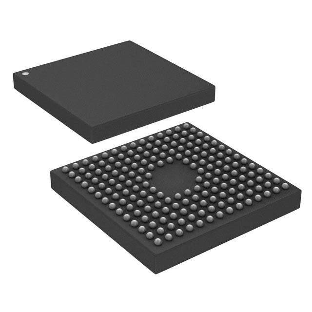
| 产品图片 |
|
| rohs | 符合RoHS无铅 / 符合限制有害物质指令(RoHS)规范要求 |
| 产品系列 | 嵌入式处理器和控制器,数字信号处理器和控制器 - DSP, DSC,Analog Devices ADSP-21060LKSZ-160SHARC® |
| 数据手册 | |
| 产品型号 | ADSP-21060LKSZ-160 |
| 产品 | DSPs |
| 产品培训模块 | http://www.digikey.cn/PTM/IndividualPTM.page?site=cn&lang=zhs&ptm=12979 |
| 产品种类 | 数字信号处理器和控制器 - DSP, DSC |
| 供应商器件封装 | 240-MQFP-EP(32x32) |
| 其它名称 | ADSP21060LKSZ160 |
| 包装 | 托盘 |
| 商标 | Analog Devices |
| 商标名 | SHARC |
| 安装类型 | 表面贴装 |
| 安装风格 | SMD/SMT |
| 封装 | Tray |
| 封装/外壳 | 240-BFQFP 裸露焊盘 |
| 封装/箱体 | QFP-240 |
| 工作温度 | 0°C ~ 85°C |
| 工作电源电压 | 4.75 V to 5.25 V |
| 工厂包装数量 | 24 |
| 接口 | 主机接口,连接端口,串行端口 |
| 数据RAM大小 | 512 kB |
| 数据总线宽度 | 32 bit |
| 时钟速率 | 40MHz |
| 最大工作温度 | + 85 C |
| 最大时钟频率 | 40 MHz |
| 最小工作温度 | 0 C |
| 标准包装 | 1 |
| 核心 | SHARC |
| 片载RAM | 512kB |
| 电压-I/O | 3.30V |
| 电压-内核 | 3.30V |
| 程序存储器大小 | 4 MB |
| 类型 | 浮点 |
| 系列 | ADSP-21060L |
| 非易失性存储器 | 外部 |


PDF Datasheet 数据手册内容提取
SHARC Processor ADSP-21060/ADSP-21060L/ADSP-21062/ADSP-21062L/ADSP-21060C/ADSP-21060LC SUMMARY KEY FEATURES—PROCESSOR CORE High performance signal processor for communications, 40 MIPS, 25 ns instruction rate, single-cycle instruction graphics and imaging applications execution Super Harvard Architecture 120 MFLOPS peak, 80 MFLOPS sustained performance 4 independent buses for dual data fetch, instruction fetch, Dual data address generators with modulo and bit-reverse and nonintrusive I/O addressing) 32-bit IEEE floating-point computation units—multiplier, Efficient program sequencing with zero-overhead looping: ALU, and shifter Single-cycle loop setup Dual-ported on-chip SRAM and integrated I/O peripherals—a IEEE JTAG Standard 1149.1 Test Access Port and on-chip complete system-on-a-chip emulation Integrated multiprocessing features 32-bit single-precision and 40-bit extended-precision IEEE 240-lead thermally enhanced MQFP_PQ4 package, 225-ball floating-point data formats or 32-bit fixed-point data plastic ball grid array (PBGA), 240-lead hermetic CQFP format package RoHS compliant packages CORE PROCESSOR DUAL-PORTED SRAM TIMER IN3S2CT R(cid:19)AUC 4CH8TE-BIOITN DUTAWLO-P IONRDTEEPDE NBDLOENCTKS OCK 0 K 1 TEJSTTA GAND 7 PROCESSOR PORT I/O PORT BL OC EMULATION ADDR DATA DATA ADDR BL ADDR DATA DATA ADDR DAG1 DAG2 PROGRAM 8 (cid:19) 4 (cid:19) 32 8 (cid:19) 4 (cid:19) 24 SEQUENCER EXTERNAL IOD IOA PORT PM ADDRESS BUS 24 48 17 32 ADDR BUS DM ADDRESS BUS 32 MUX MULTIPROCESSOR INTERFACE PM DATA BUS 48 BUS 48 DATA BUS CO(NPNX)ECT DM DATA BUS 40/32 MUX S HOST PORT DATA DMA 4 IOP REGISTER REGISTERS CONTROLLER FILE 6 (MEMORY MULT 16 (cid:19) 40-BIT SBHAIRFRTEERL ALU MCOANPPTREOD)L, SERIA(L2 )PORTS 6 STATUS AND 36 LINK PORTS DATA BUFFERS (6) I/O PROCESSOR Figure 1. Functional Block Diagram SHARC and the SHARC logo are registered trademarks of Analog Devices, Inc. Rev. H Document Feedback Information furnished by Analog Devices is believed to be accurate and reliable. However, no responsibility is assumed by Analog Devices for its use, nor for any infringements of patents or other rights of third parties that may result from its use. Specifications subject to change without notice. No license is granted by implication One Technology Way, P.O. Box 9106, Norwood, MA 02062-9106 U.S.A. or otherwise under any patent or patent rights of Analog Devices. Trademarks and Tel: 781.329.4700 ©2013 Analog Devices, Inc. All rights reserved. registered trademarks are the property of their respective owners. Technical Support www.analog.com
ADSP-21060/ADSP-21060L/ADSP-21062/ADSP-21062L/ADSP-21060C/ADSP-21060LC PARALLEL COMPUTATIONS HOST PROCESSOR INTERFACE TO 16- AND 32-BIT MICROPROCESSORS Single-cycle multiply and ALU operations in parallel with dual memory read/writes and instruction fetch Host can directly read/write ADSP-2106x internal memory Multiply with add and subtract for accelerated FFT butterfly and IOP registers computation MULTIPROCESSING UP TO 4M BIT ON-CHIP SRAM Glueless connection for scalable DSP multiprocessing Dual-ported for independent access by core processor and architecture DMA Distributed on-chip bus arbitration for parallel bus connect OFF-CHIP MEMORY INTERFACING of up to six ADSP-2106xs plus host Six link ports for point-to-point connectivity and array 4 gigawords addressable multiprocessing Programmable wait state generation, page-mode DRAM 240 MBps transfer rate over parallel bus support 240 MBps transfer rate over link ports DMA CONTROLLER SERIAL PORTS 10 DMA channels for transfers between ADSP-2106x internal Two 40 Mbps synchronous serial ports with companding memory and external memory, external peripherals, host hardware processor, serial ports, or link ports Independent transmit and receive functions Background DMA transfers at up to 40 MHz, in parallel with full-speed processor execution Table 1. ADSP-2106x SHARC Processor Family Features Feature ADSP-21060 ADSP-21062 ADSP-21060L ADSP-21062L ADSP-21060C ADSP-21060LC SRAM 4M bits 2M bits 4M bits 2M bits 4M bits 4M bits Operating Voltage 5 V 5 V 3.3 V 3.3 V 5 V 3.3 V Instruction 33 MHz 33 MHz 33 MHz 33 MHz 33 MHz 33 MHz Rate 40 MHz 40 MHz 40 MHz 40 MHz 40 MHz 40 MHz MQFP_PQ4 MQFP_PQ4 MQFP_PQ4 MQFP_PQ4 Package PBGA PBGA PBGA PBGA CQFP CQFP Rev. H | Page 2 of 64 | March 2013
ADSP-21060/ADSP-21060L/ADSP-21062/ADSP-21062L/ADSP-21060C/ADSP-21060LC CONTENTS Summary ............................................................... 1 Electrical Characteristics (3.3 V) ............................. 18 General Description ................................................. 4 Internal Power Dissipation (3.3 V) .......................... 19 SHARC Family Core Architecture ............................ 4 External Power Dissipation (3.3 V) .......................... 20 Memory and I/O Interface Features ........................... 5 Absolute Maximum Ratings ................................... 20 Development Tools ............................................... 8 ESD Caution ...................................................... 21 Additional Information .......................................... 9 Package Marking Information ................................ 21 Related Signal Chains ............................................ 9 Timing Specifications ........................................... 21 Pin Function Descriptions ........................................ 10 Test Conditions .................................................. 48 Target Board Connector for EZ-ICE Probe ................ 13 Environmental Conditions .................................... 51 ADSP-21060/ADSP-21062 Specifications ..................... 15 225-Ball PBGA Ball Configuration .............................. 52 Operating Conditions (5 V) .................................... 15 240-Lead MQFP_PQ4/CQFP Pin Configuration ............ 54 Electrical Characteristics (5 V) ................................ 15 Outline Dimensions ................................................ 56 Internal Power Dissipation (5 V) ............................. 16 Surface-Mount Design .......................................... 61 External Power Dissipation (5 V) ............................. 17 Ordering Guide ..................................................... 62 ADSP-21060L/ADSP-21062L Specifications .................. 18 Operating Conditions (3.3 V) ................................. 18 REVISION HISTORY 3/13—Rev. G to Rev. H Updated Development Tools .......................................8 Corrected the power dissipation equation from P = P + TOTAL EXT (IDDIN2 5.0 V) to PTOTAL = PEXT + (IDDIN2 3.3 V) External Power Dissipation (3.3 V) .............................20 Rev. H | Page 3 of 64 | March 2013
ADSP-21060/ADSP-21060L/ADSP-21062/ADSP-21062L/ADSP-21060C/ADSP-21060LC GENERAL DESCRIPTION The ADSP-2106x SHARC®—Super Harvard Architecture Com- • Serial ports and link ports puter—is a 32-bit signal processing microcomputer that offers • JTAG Test Access Port high levels of DSP performance. The ADSP-2106x builds on the ADSP-21000 DSP core to form a complete system-on-a-chip, adding a dual-ported on-chip SRAM and integrated I/O periph- erals supported by a dedicated I/O bus. ADSP-2106x Fabricated in a high speed, low power CMOS process, the 1(cid:2)CLOCK CLKIN BMS CS BOOT ADSP-2106x has a 25 ns instruction cycle time and operates at EBOOT ADDR(OEPPTIROONMAL) 40 MIPS. With its on-chip instruction cache, the processor can 3 LBOOT DATA IRQ2–0 execute every instruction in a single cycle. Table2 shows perfor- 4 FLAG3–0 ADDR31–0 ADDR mance benchmarks for the ADSP-2106x. TIMEXP DATA47–0 DATA MEMORY- The ADSP-2106x SHARC represents a new standard of integra- LINK LxCLK RD OE DMEAVPIPCEEDS tion for signal computers, combining a high performance D(6EVMIACXES) LxACK AWCKR AWCEK (OPTIONAL) floating-point DSP core with integrated, on-chip system fea- (OPTIONAL) LxDAT3–0 MS3–0 CS thpmuoourrselttts, i p apirnnrocodclc uepesdsasisronianrgl lgi eun.lpt be truofsa 4ccMeo,n DnbiMetc StAiRv cAitoyMn fto rmor leglmeluro,e slreeysr s(i asDel epS PoTr atbs laen1d) ,l ain k (ODSPEETRIVOIIACNELAL) TDRTRCFTSCSL0FL0K0K00 ADPRSACBGLTKES TLNRCOO SSEADDR TDAA DATAD(OMPATDIOENVAICLE) DR0 DMAR1–2 DMAG1–2 Table 2. Benchmarks (at 40 MHz) TCLK1 SERIAL RCLK1 CS (ODPTEIVOICNEAL) DRTFTSS1F11 HHBBGR PINRTOHECORESFSATSCOER Benchmark Algorithm Speed Cycles DR1 REDY (OPTIONAL) 1024 Point Complex FFT (Radix 4, with 0.46 s 18,221 RPBA BR1–6 ADDR reversal) ID2–0 PA DATA FIR Filter (per tap) 25 ns 1 RESET JTAG IIR Filter (per biquad) 100 ns 4 6 Divide (y/x) 150 ns 6 Inverse Square Root 225 ns 9 Figure 2. ADSP-2106x System Sample Configuration DMA Transfer Rate 240 Mbytes/s SHARC FAMILY CORE ARCHITECTURE The ADSP-2106x continues SHARC’s industry-leading stan- The ADSP-2106x includes the following architectural features dards of integration for DSPs, combining a high performance of the ADSP-21000 family core. 32-bit DSP core with integrated, on-chip system features. Independent, Parallel Computation Units The block diagram onPage1 illustrates the following architec- tural features: The arithmetic/logic unit (ALU), multiplier and shifter all per- form single-cycle instructions. The three units are arranged in • Computation units (ALU, multiplier and shifter) with a parallel, maximizing computational throughput. Single multi- shared data register file function instructions execute parallel ALU and multiplier oper- • Data address generators (DAG1, DAG2) ations. These computation units support IEEE 32-bit single- • Program sequencer with instruction cache precision floating-point, extended precision 40-bit floating- point, and 32-bit fixed-point data formats. • PM and DM buses capable of supporting four 32-bit data transfers between memory and the core at every core pro- Data Register File cessor cycle A general–purpose data register file is used for transferring data • Interval timer between the computation units and the data buses, and for stor- • On-chip SRAM ing intermediate results. This 10-port, 32-register (16 primary, 16 secondary) register file, combined with the ADSP-21000 • External port for interfacing to off-chip memory and Harvard architecture, allows unconstrained data flow between peripherals computation units and internal memory. • Host port and multiprocessor Interface • DMA controller Rev. H | Page 4 of 64 | March 2013
ADSP-21060/ADSP-21060L/ADSP-21062/ADSP-21062L/ADSP-21060C/ADSP-21060LC Single-Cycle Fetch of Instruction and Two Operands On the ADSP-21060/ADSP-21060L, the memory can be config- ured as a maximum of 128k words of 32-bit data, 256k words of The ADSP-2106x features an enhanced Harvard architecture in 16-bit data, 80k words of 48-bit instructions (or 40-bit data), or which the data memory (DM) bus transfers data and the pro- combinations of different word sizes up to four megabits. All of gram memory (PM) bus transfers both instructions and data the memory can be accessed as 16-bit, 32-bit or 48-bit words. (see Figure1 on Page1). With its separate program and data memory buses and on-chip instruction cache, the processor can A 16-bit floating-point storage format is supported, which effec- simultaneously fetch two operands and an instruction (from the tively doubles the amount of data that can be stored on-chip. cache), all in a single cycle. Conversion between the 32-bit floating-point and 16-bit float- ing-point formats is done in a single instruction. Instruction Cache While each memory block can store combinations of code and The ADSP-2106x includes an on-chip instruction cache that data, accesses are most efficient when one block stores data, enables three-bus operation for fetching an instruction and two using the DM bus for transfers, and the other block stores data values. The cache is selective—only the instructions whose instructions and data, using the PM bus for transfers. Using the fetches conflict with PM bus data accesses are cached. This DM bus and PM bus in this way, with one dedicated to each allows full-speed execution of core, looped operations such as memory block, assures single-cycle execution with two data digital filter multiply-accumulates and FFT butterfly processing. transfers. In this case, the instruction must be available in the cache. Single-cycle execution is also maintained when one of the Data Address Generators with Hardware Circular Buffers data operands is transferred to or from off-chip, via the The ADSP-2106x’s two data address generators (DAGs) imple- ADSP-2106x’s external port. ment circular data buffers in hardware. Circular buffers allow On-Chip Memory and Peripherals Interface efficient programming of delay lines and other data structures required in digital signal processing, and are commonly used in The ADSP-2106x’s external port provides the processor’s inter- digital filters and Fourier transforms. The two DAGs of the face to off-chip memory and peripherals. The 4-gigaword off- ADSP-2106x contain sufficient registers to allow the creation of chip address space is included in the ADSP-2106x’s unified up to 32 circular buffers (16 primary register sets, 16 secondary). address space. The separate on-chip buses—for PM addresses, The DAGs automatically handle address pointer wraparound, PM data, DM addresses, DM data, I/O addresses, and I/O reducing overhead, increasing performance and simplifying data—are multiplexed at the external port to create an external implementation. Circular buffers can start and end at any mem- system bus with a single 32-bit address bus and a single 48-bit ory location. (or 32-bit) data bus. Flexible Instruction Set Addressing of external memory devices is facilitated by on-chip decoding of high-order address lines to generate memory bank The 48-bit instruction word accommodates a variety of select signals. Separate control lines are also generated for sim- parallel operations, for concise programming. For example, the plified addressing of page-mode DRAM. The ADSP-2106x ADSP-2106x can conditionally execute a multiply, an add, a provides programmable memory wait states and external mem- subtract and a branch, all in a single instruction. ory acknowledge controls to allow interfacing to DRAM and MEMORY AND I/O INTERFACE FEATURES peripherals with variable access, hold and disable time requirements. The ADSP-2106x processors add the following architectural features to the SHARC family core. Host Processor Interface Dual-Ported On-Chip Memory The ADSP-2106x’s host interface allows easy connection to standard microprocessor buses, both 16-bit and 32-bit, with lit- The ADSP-21062/ADSP-21062L contains two megabits of on- tle additional hardware required. Asynchronous transfers at chip SRAM, and the ADSP-21060/ADSP-21060L contains speeds up to the full clock rate of the processor are supported. 4M bits of on-chip SRAM. The internal memory is organized as The host interface is accessed through the ADSP-2106x’s exter- two equal sized blocks of 1M bit each for the ADSP-21062/ nal port and is memory-mapped into the unified address space. ADSP-21062L and two equal sized blocks of 2M bits each for Four channels of DMA are available for the host interface; code the ADSP-21060/ADSP-21060L. Each can be configured for dif- and data transfers are accomplished with low software ferent combinations of code and data storage. Each memory overhead. block is dual-ported for single-cycle, independent accesses by The host processor requests the ADSP-2106x’s external bus with the core processor and I/O processor or DMA controller. The the host bus request (HBR), host bus grant (HBG), and ready dual-ported memory and separate on-chip buses allow two data (REDY) signals. The host can directly read and write the inter- transfers from the core and one from I/O, all in a single cycle. nal memory of the ADSP-2106x, and can access the DMA On the ADSP-21062/ADSP-21062L, the memory can be config- channel setup and mailbox registers. Vector interrupt support is ured as a maximum of 64k words of 32-bit data, 128k words of provided for efficient execution of host commands. 16-bit data, 40k words of 48-bit instructions (or 40-bit data), or combinations of different word sizes up to two megabits. All of the memory can be accessed as 16-bit, 32-bit, or 48-bit words. Rev. H | Page 5 of 64 | March 2013
ADSP-21060/ADSP-21060L/ADSP-21062/ADSP-21062L/ADSP-21060C/ADSP-21060LC ADSP-2106x#6 ADSP-2106x#5 ADSP-2106x#4 L S ADSP-2106x#3 CNTORO ADDESR DTAA CLKIN ADDR31–0 DATA47–0 RESET RPBA 3 ID2–0 CONTROL 011 5 BR1–2,BR4–6 BR3 ADSP-2106x#2 CLKIN ADDR31–0 DATA47–0 RESET RPBA 3 ID2–0 CONTROL 010 CPA 5 BR1,BR3–6 BR2 L S ADSP-2106x#1 TNORO DDRES DATA C A CLKIN ADDR31–0 ADDR RESET DATA47–0 DATA GLOBALMEMORY AND RPBA RDx OE PERIPHERAL(OPTIONAL) WRx WE 3 ACK ACK ID2–0 LRO MS3–0 CS T N 001 CO BMS CS PAGE ADDR BOOTEPROM(OPTIONAL) SBTS DATA BUS PRIORITY CS HBR RESET HBG HOSTPROCESSOR CLOCK REDY INTERFACE(OPTIONAL) ADDR CPA BR2–6 5 DATA BR1 Figure 3. Shared Memory Multiprocessing System Rev. H | Page 6 of 64 | March 2013
ADSP-21060/ADSP-21060L/ADSP-21062/ADSP-21062L/ADSP-21060C/ADSP-21060LC DMA Controller control two DMA channels using DMA request/grant lines (DMAR1–2, DMAG1–2). Other DMA features include inter- The ADSP-2106x’s on-chip DMA controller allows zero-over- rupt generation upon completion of DMA transfers and DMA head data transfers without processor intervention. The DMA chaining for automatic linked DMA transfers. controller operates independently and invisibly to the processor core, allowing DMA operations to occur while the core is simul- Multiprocessing taneously executing its program instructions. The ADSP-2106x offers powerful features tailored to multipro- DMA transfers can occur between the ADSP-2106x’s internal cessor DSP systems. The unified address space (see Figure4) memory and external memory, external peripherals, or a host allows direct interprocessor accesses of each ADSP-2106x’s processor. DMA transfers can also occur between the ADSP- internal memory. Distributed bus arbitration logic is included 2106x’s internal memory and its serial ports or link ports. DMA on-chip for simple, glueless connection of systems containing transfers between external memory and external peripheral up to six ADSP-2106xs and a host processor. Master processor devices are another option. External bus packing to 16-, changeover incurs only one cycle of overhead. Bus arbitration is 32-, or 48-bit words is performed during DMA transfers. selectable as either fixed or rotating priority. Bus lock allows Ten channels of DMA are available on the ADSP-2106x—two indivisible read-modify-write sequences for semaphores. A vec- via the link ports, four via the serial ports, and four via the tor interrupt is provided for interprocessor commands. Maxi- processor’s external port (for either host processor, other mum throughput for interprocessor data transfer is ADSP-2106xs, memory, or I/O transfers). Four additional link 240M bytes/s over the link ports or external port. Broadcast port DMA channels are shared with Serial Port 1 and the exter- writes allow simultaneous transmission of data to all nal port. Programs can be downloaded to the ADSP-2106x ADSP-2106xs and can be used to implement reflective using DMA transfers. Asynchronous off-chip peripherals can semaphores. ADDRESS ADDRESS 0x00000000 IOPREGISTERS 0x00400000 INTERNAL NORMALWORDADDRESSING 0x00020000 MEMORY (32-BITDATAWORDS BANK 0 MS0 SPACE 48-BITINSTRUCTIONWORDS) 0x00040000 SRAM (OPTIONAL) SHORTWORDADDRESSING (16-BITDATAWORDS) 0x00080000 INTERNALMEMORYSPACE BANK 1 MS1 WITHID=001 0x00100000 INTERNALMEMORYSPACE WITHID=010 0x00180000 INTERNALMEMORYSPACE EXTERNAL BANK 2 MS2 MULTIPROCESSOR WITHID=011 MEMORY MEMORY SPACE SPACE 0x00120000 INTERNALMEMORYSPACE WITHID=100 0x00280000 INTERNALMEMORYSPACE BANK 3 MS3 WITHID=101 0x00300000 INTERNALMEMORYSPACE WITHID=110 0x00380000 BROADCASTWRITE NONBANKED TOALLADSP-21061s 0x003FFFFF 0x0FFFFFFF NOTE:BANKSIZESARESELECTEDBY MSIZEBITSINTHESYSCONREGISTER Figure 4. Memory Map Rev. H | Page 7 of 64 | March 2013
ADSP-21060/ADSP-21060L/ADSP-21062/ADSP-21062L/ADSP-21060C/ADSP-21060LC Link Ports emulation capabilities and other evaluation and development features. Also available are various EZ-Extenders®, which are The ADSP-2106x features six 4-bit link ports that provide addi- daughter cards delivering additional specialized functionality, tional I/O capabilities. The link ports can be clocked twice per including audio and video processing. For more information cycle, allowing each to transfer eight bits of data per cycle. Link- visit www.analog.com and search on “ezkit” or “ezextender”. port I/O is especially useful for point-to-point interprocessor communication in multiprocessing systems. EZ-KIT Lite Evaluation Kits The link ports can operate independently and simultaneously, For a cost-effective way to learn more about developing with with a maximum data throughput of 240M bytes/s. Link port Analog Devices processors, Analog Devices offer a range of EZ- data is packed into 32- or 48-bit words, and can be directly read KIT Lite evaluation kits. Each evaluation kit includes an EZ-KIT by the core processor or DMA-transferred to on-chip memory. Lite evaluation board, directions for downloading an evaluation Each link port has its own double-buffered input and output version of the available IDE(s), a USB cable, and a power supply. registers. Clock/acknowledge handshaking controls link port The USB controller on the EZ-KIT Lite board connects to the transfers. Transfers are programmable as either transmit or USB port of the user’s PC, enabling the chosen IDE evaluation receive. suite to emulate the on-board processor in-circuit. This permits the customer to download, execute, and debug programs for the Program Booting EZ-KIT Lite system. It also supports in-circuit programming of The internal memory of the ADSP-2106x can be booted at sys- the on-board Flash device to store user-specific boot code, tem power-up from an 8-bit EPROM, a host processor, or enabling standalone operation. With the full version of Cross- through one of the link ports. Selection of the boot source is Core Embedded Studio or VisualDSP++ installed (sold controlled by the BMS (boot memory select), EBOOT (EPROM separately), engineers can develop software for supported EZ- Boot), and LBOOT (link/host boot) pins. 32-bit and 16-bit host KITs or any custom system utilizing supported Analog Devices processors can be used for booting. The processor also sup- processors. ports a no-boot mode in which instruction execution is sourced Software Add-Ins for CrossCore Embedded Studio from the external memory. Analog Devices offers software add-ins which seamlessly inte- DEVELOPMENT TOOLS grate with CrossCore Embedded Studio to extend its capabilities Analog Devices supports its processors with a complete line of and reduce development time. Add-ins include board support software and hardware development tools, including integrated packages for evaluation hardware, various middleware pack- development environments (which include CrossCore® Embed- ages, and algorithmic modules. Documentation, help, ded Studio and/or VisualDSP++®), evaluation products, configuration dialogs, and coding examples present in these emulators, and a wide variety of software add-ins. add-ins are viewable through the CrossCore Embedded Studio IDE once the add-in is installed. Integrated Development Environments (IDEs) Board Support Packages for Evaluation Hardware For C/C++ software writing and editing, code generation, and debug support, Analog Devices offers two IDEs. Software support for the EZ-KIT Lite evaluation boards and EZ- Extender daughter cards is provided by software add-ins called The newest IDE, CrossCore Embedded Studio, is based on the Board Support Packages (BSPs). The BSPs contain the required EclipseTM framework. Supporting most Analog Devices proces- drivers, pertinent release notes, and select example code for the sor families, it is the IDE of choice for future processors, given evaluation hardware. A download link for a specific BSP is including multicore devices. CrossCore Embedded Studio located on the web page for the associated EZ-KIT or EZ- seamlessly integrates available software add-ins to support real Extender product. The link is found in the Product Download time operating systems, file systems, TCP/IP stacks, USB stacks, area of the product web page. algorithmic software modules, and evaluation hardware board support packages. For more information visit Middleware Packages www.analog.com/cces. Analog Devices separately offers middleware add-ins such as The other Analog Devices IDE, VisualDSP++, supports proces- real time operating systems, file systems, USB stacks, and sor families introduced prior to the release of CrossCore TCP/IP stacks. For more information see the following web Embedded Studio. This IDE includes the Analog Devices VDK pages: real time operating system and an open source TCP/IP stack. • www.analog.com/ucos3 For more information visit www.analog.com/visualdsp. Note that VisualDSP++ will not support future Analog Devices • www.analog.com/ucfs processors. • www.analog.com/ucusbd EZ-KIT Lite Evaluation Board • www.analog.com/lwip For processor evaluation, Analog Devices provides wide range of EZ-KIT Lite® evaluation boards. Including the processor and key peripherals, the evaluation board also supports on-chip Rev. H | Page 8 of 64 | March 2013
ADSP-21060/ADSP-21060L/ADSP-21062/ADSP-21062L/ADSP-21060C/ADSP-21060LC Algorithmic Modules The Application Signal Chains page in the Circuits from the LabTM site (http://www.analog.com/signalchains) provides: To speed development, Analog Devices offers add-ins that per- form popular audio and video processing algorithms. These are • Graphical circuit block diagram presentation of signal available for use with both CrossCore Embedded Studio and chains for a variety of circuit types and applications VisualDSP++. For more information visit www.analog.com • Drill down links for components in each chain to selection and search on “Blackfin software modules” or “SHARC software guides and application information modules”. • Reference designs applying best practice design techniques Designing an Emulator-Compatible DSP Board(Target) For embedded system test and debug, Analog Devices provides a family of emulators. On each JTAG DSP, Analog Devices sup- plies an IEEE 1149.1 JTAG Test Access Port (TAP). In-circuit emulation is facilitated by use of this JTAG interface. The emu- lator accesses the processor’s internal features via the processor’s TAP, allowing the developer to load code, set break- points, and view variables, memory, and registers. The processor must be halted to send data and commands, but once an operation is completed by the emulator, the DSP system is set to run at full speed with no impact on system timing. The emu- lators require the target board to include a header that supports connection of the DSP’s JTAG port to the emulator. For details on target board design issues including mechanical layout, single processor connections, signal buffering, signal ter- mination, and emulator pod logic, see the EE-68: Analog Devices JTAG Emulation Technical Reference on the Analog Devices website (www.analog.com)—use site search on “EE-68.” This document is updated regularly to keep pace withimprovements to emulator support. ADDITIONAL INFORMATION This data sheet provides a general overview of the ADSP-2106x architecture and functionality. For detailed information on the ADSP-21000 family core architecture and instruction set, refer to the ADSP-2106x SHARC User’s Manual, Revision 2.1. RELATED SIGNAL CHAINS A signal chain is a series of signal-conditioning electronic com- ponents that receive input (data acquired from sampling either real-time phenomena or from stored data) in tandem, with the output of one portion of the chain supplying input to the next. Signal chains are often used in signal processing applications to gather and process data or to apply system controls based on analysis of real-time phenomena. For more information about this term and related topics, see the “signal chain” entry in the Glossary of EE Terms on the Analog Devices website. Analog Devices eases signal processing system development by providing signal processing components that are designed to work together well. A tool for viewing relationships between specific applications and related components is available on the www.analog.com website. Rev. H | Page 9 of 64 | March 2013
ADSP-21060/ADSP-21060L/ADSP-21062/ADSP-21062L/ADSP-21060C/ADSP-21060LC PIN FUNCTION DESCRIPTIONS The ADSP-2106x pin definitions are listed below. Inputs identi- Unused inputs should be tied or pulled to VDD or GND, except fied as synchronous (S) must meet timing requirements with for ADDR31–0, DATA47–0, FLAG3–0, and inputs that have respect to CLKIN (or with respect to TCK for TMS, TDI). internal pull-up or pull-down resistors (CPA, ACK, DTx, DRx, Inputs identified as asynchronous (A) can be asserted asynchro- TCLKx, RCLKx, LxDAT3–0, LxCLK, LxACK, TMS, and nously to CLKIN (or to TCK for TRST). TDI)—these pins can be left floating. These pins have a logic-level hold circuit that prevents the input from floating internally. Table 3. Pin Descriptions Pin Type Function ADDR31–0 I/O/T External Bus Address. The ADSP-2106x outputs addresses for external memory and peripherals on these pins. In a multiprocessor system, the bus master outputs addresses for read/write of the internal memory or IOP registers of other ADSP-2106xs. The ADSP-2106x inputs addresses when a host processor or multi- processing bus master is reading or writing its internal memory or IOP registers. DATA47–0 I/O/T External Bus Data. The ADSP-2106x inputs and outputs data and instructions on these pins. 32-bit single- precision floating-point data and 32-bit fixed-point data is transferred over bits 47–16 of the bus. 40-bit extended-precision floating-point data is transferred over bits 47–8 of the bus. 16-bit short word data is transferred over bits 31–16 of the bus. In PROM boot mode, 8-bit data is transferred over bits 23–16. Pull-up resistors on unused DATA pins are not necessary. MS3–0 O/T Memory Select Lines. These lines are asserted (low) as chip selects for the corresponding banks of external memory. Memory bank size must be defined in the ADSP-2106x’s system control register (SYSCON). The MS3–0 lines are decoded memory address lines that change at the same time as the other address lines. When no external memory access is occurring, the MS3–0 lines are inactive; they are active however when a conditional memory access instruction is executed, whether or not the condition is true. MS0 can be used with the PAGE signal to implement a bank of DRAM memory (Bank 0). In a multiprocessing system the MS3–0 lines are output by the bus master. RD I/O/T Memory Read Strobe. This pin is asserted (low) when the ADSP-2106x reads from external memory devices or from the internal memory of other ADSP-2106xs. External devices (including other ADSP-2106xs) must assert RD to read from the ADSP-2106x’s internal memory. In a multiprocessing system, RD is output by the bus master and is input by all other ADSP-2106xs. WR I/O/T Memory Write Strobe. This pin is asserted (low) when the ADSP-2106x writes to external memory devices or to the internal memory of other ADSP-2106xs. External devices must assert WR to write to the ADSP- 2106x’s internal memory. In a multiprocessing system, WR is output by the bus master and is input by all other ADSP-2106xs. PAGE O/T DRAM Page Boundary. The ADSP-2106x asserts this pin to signal that an external DRAM page boundary has been crossed. DRAM page size must be defined in the ADSP-2106x’s memory control register (WAIT). DRAM can only be implemented in external memory Bank 0; the PAGE signal can only be activated for Bank 0 accesses. In a multiprocessing system, PAGE is output by the bus master ADRCLK O/T Clock Output Reference. In a multiprocessing system, ADRCLK is output by the bus master. SW I/O/T Synchronous Write Select. This signal is used to interface the ADSP-2106x to synchronous memory devices (including other ADSP-2106xs). The ADSP-2106x asserts SW (low) to provide an early indication of an impending write cycle, which can be aborted if WR is not later asserted (e.g., in a conditional write instruction). In a multiprocessing system, SW is output by the bus master and is input by all other ADSP-2106xs to determine if the multiprocessor memory access is a read or write. SW is asserted at the same time as the address output. A host processor using synchronous writes must assert this pin when writing to the ADSP-2106x(s). A = Asynchronous, G = Ground, I = Input, O = Output, P = Power Supply, S = Synchronous, (A/D) = Active Drive, (O/D) = Open Drain, T = Three-State (when SBTS is asserted, or when the ADSP-2106x is a bus slave) Rev. H | Page 10 of 64 | March 2013
ADSP-21060/ADSP-21060L/ADSP-21062/ADSP-21062L/ADSP-21060C/ADSP-21060LC Table 3. Pin Descriptions (Continued) Pin Type Function ACK I/O/S Memory Acknowledge. External devices can deassert ACK (low) to add wait states to an external memory access. ACK is used by I/O devices, memory controllers, or other peripherals to hold off completion of an external memory access. The ADSP-2106x deasserts ACK as an output to add waitstates to a synchronous access of its internal memory. In a multiprocessing system, a slave ADSP-2106x deasserts the bus master’s ACK input to add wait state(s) to an access of its internal memory. The bus master has a keeper latch on its ACK pin that maintains the input at the level to which it was last driven. SBTS I/S Suspend Bus Three-State. External devices can assert SBTS (low) to place the external bus address, data, selects, and strobes in a high impedance state for the following cycle. If the ADSP-2106x attempts to access external memory while SBTS is asserted, the processor will halt and the memory access will not be completed until SBTS is deasserted. SBTS should only be used to recover from host processor/ADSP-2106x deadlock, or used with a DRAM controller. IRQ2–0 I/A Interrupt Request Lines. May be either edge-triggered or level-sensitive. FLAG3–0 I/O/A Flag Pins. Each is configured via control bits as either an input or output. As an input, they can be tested as a condition. As an output, they can be used to signal external peripherals. TIMEXP O Timer Expired. Asserted for four cycles when the timer is enabled and TCOUNT decrements to zero. HBR I/A Host Bus Request. This pin must be asserted by a host processor to request control of the ADSP-2106x’s external bus. When HBR is asserted in a multiprocessing system, the ADSP-2106x that is bus master will relinquish the bus and assert HBG. To relinquish the bus, the ADSP-2106x places the address, data, select and strobe lines in a high impedance state. HBR has priority over all ADSP-2106x bus requests BR6–1 in a multiprocessing system. HBG I/O Host Bus Grant. Acknowledges a bus request, indicating that the host processor may take control of the external bus. HBG is asserted (held low) by the ADSP-2106x until HBR is released. In a multiprocessing system, HBG is output by the ADSP-2106x bus master and is monitored by all others. CS I/A Chip Select. Asserted by host processor to select the ADSP-2106x. REDY O (O/D) Host Bus Acknowledge. The ADSP-2106x deasserts REDY (low) to add wait states to an asynchronous access of its internal memory or IOP registers by a host. This pin is an open-drain output (O/D) by default; it can be programmed in the ADREDY bit of the SYSCON register to be active drive (A/D). REDY will only be output if the CS and HBR inputs are asserted. DMAR2–1 I/A DMA Request 1 (DMA Channel 7) and DMA Request 2 (DMA Channel 8). DMAG2–1 O/T DMA Grant 1 (DMA Channel 7) and DMA Grant 2 (DMA Channel 8). BR6–1 I/O/S Multiprocessing Bus Requests. Used by multiprocessing ADSP-2106xs to arbitrate for bus master-ship. An ADSP-2106x only drives its own BRx line (corresponding to the value of its ID2-0 inputs) and monitors all others. In a multiprocessor system with less than six ADSP-2106xs, the unused BRx pins should be pulled high; the processor’s own BRx line must not be pulled high or low because it is an output. ID2–0 O (O/D) Multiprocessing ID. Determines which multiprocessing bus request (BR1– BR6) is used by ADSP-2106x. ID = 001 corresponds to BR1, ID = 010 corresponds to BR2, etc. ID = 000 in single-processor systems. These lines are a system configuration selection that should be hardwired or changed at reset only. RPBA I/S Rotating Priority Bus Arbitration Select. When RPBA is high, rotating priority for multiprocessor bus arbitration is selected. When RPBA is low, fixed priority is selected. This signal is a system configuration selection that must be set to the same value on every ADSP-2106x. If the value of RPBA is changed during system operation, it must be changed in the same CLKIN cycle on every ADSP-2106x. CPA I/O (O/D) Core Priority Access. Asserting its CPA pin allows the core processor of an ADSP-2106x bus slave to interrupt background DMA transfers and gain access to the external bus. CPA is an open drain output that is connected to all ADSP-2106xs in the system. The CPA pin has an internal 5 k pull-up resistor. If core access priority is not required in a system, the CPA pin should be left unconnected. DTx O Data Transmit (Serial Ports 0, 1). Each DT pin has a 50 k internal pull-up resistor. DRx I Data Receive (Serial Ports 0, 1). Each DR pin has a 50 k internal pull-up resistor. TCLKx I/O Transmit Clock (Serial Ports 0, 1). Each TCLK pin has a 50 k internal pull-up resistor. RCLKx I/O Receive Clock (Serial Ports 0, 1). Each RCLK pin has a 50 k internal pull-up resistor. A = Asynchronous, G = Ground, I = Input, O = Output, P = Power Supply, S = Synchronous, (A/D) = Active Drive, (O/D) = Open Drain, T = Three-State (when SBTS is asserted, or when the ADSP-2106x is a bus slave) Rev. H | Page 11 of 64 | March 2013
ADSP-21060/ADSP-21060L/ADSP-21062/ADSP-21062L/ADSP-21060C/ADSP-21060LC Table 3. Pin Descriptions (Continued) Pin Type Function TFSx I/O Transmit Frame Sync (Serial Ports 0, 1). RFSx I/O Receive Frame Sync (Serial Ports 0, 1). LxDAT3–0 I/O Link Port Data (Link Ports 0–5). Each LxDAT pin has a 50 k internal pull-down resistor that is enabled or disabled by the LPDRD bit of the LCOM register. LxCLK I/O Link Port Clock (Link Ports 0–5). Each LxCLK pin has a 50 k internal pull-down resistor that is enabled or disabled by the LPDRD bit of the LCOM register. LxACK I/O Link Port Acknowledge (Link Ports 0–5). Each LxACK pin has a 50 k internal pull-down resistor that is enabled or disabled by the LPDRD bit of the LCOM register. EBOOT I EPROM Boot Select. When EBOOT is high, the ADSP-2106x is configured for booting from an 8-bit EPROM. When EBOOT is low, the LBOOT and BMS inputs determine booting mode. See the table in the BMS pin description below. This signal is a system configuration selection that should be hardwired. LBOOT I Link Boot. When LBOOT is high, the ADSP-2106x is configured for link port booting. When LBOOT is low, the ADSP-2106x is configured for host processor booting or no booting. See the table in the BMS pin description below. This signal is a system configuration selection that should be hardwired. BMS I/OT Boot Memory Select. Output: Used as chip select for boot EPROM devices (when EBOOT = 1, LBOOT = 0). In a multiprocessor system, BMS is output by the bus master. Input: When low, indicates that no booting will occur and that ADSP-2106x will begin executing instructions from external memory. See table below. This input is a system configuration selection that should be hardwired. *Three-statable only in EPROM boot mode (when BMS is an output). EBOOT LBOOT BMS Booting Mode 1 0 Output EPROM (Connect BMS to EPROM chip select.) 0 0 1 (Input) Host Processor 0 1 1 (Input) Link Port 0 0 0 (Input) No Booting. Processor executes from external memory. 0 1 0 (Input) Reserved 1 1 x (Input) Reserved CLKIN I Clock In. External clock input to the ADSP-2106x. The instruction cycle rate is equal to CLKIN. CLKIN should not be halted, changed, or operated below the minimum specified frequency. RESET I/A Processor Reset. Resets the ADSP-2106x to a known state and begins program execution at the program memory location specified by the hardware reset vector address. This input must be asserted (low) at power-up. TCK I Test Clock (JTAG). Provides an asynchronous clock for JTAG boundary scan. TMS I/S Test Mode Select (JTAG). Used to control the test state machine. TMS has a 20 k internal pull-up resistor. TDI I/S Test Data Input (JTAG). Provides serial data for the boundary scan logic. TDI has a 20 k internal pull-up resistor. TDO O Test Data Output (JTAG). Serial scan output of the boundary scan path. TRST I/A Test Reset (JTAG). Resets the test state machine. TRST must be asserted (pulsed low) after power-up or held low for proper operation of the ADSP-2106x. TRST has a 20 k internal pull-up resistor. EMU O Emulation Status. Must be connected to the ADSP-2106x EZ-ICE target board connector only. ICSA O Reserved, leave unconnected. VDD P Power Supply; nominally 5.0 V dc for 5 V devices or 3.3 V dc for 3.3 V devices. (30 pins). GND G Power Supply Return. (30 pins). NC Do Not Connect. Reserved pins which must be left open and unconnected. A = Asynchronous, G = Ground, I = Input, O = Output, P = Power Supply, S = Synchronous, (A/D) = Active Drive, (O/D) = Open Drain, T = Three-State (when SBTS is asserted, or when the ADSP-2106x is a bus slave) Rev. H | Page 12 of 64 | March 2013
ADSP-21060/ADSP-21060L/ADSP-21062/ADSP-21062L/ADSP-21060C/ADSP-21060LC TARGET BOARD CONNECTOR FOR EZ-ICE PROBE The JTAG signals are terminated on the EZ-ICE probe as shown in Table4. The ADSP-2106x EZ-ICE® Emulator uses the IEEE 1149.1JTAG test access port of the ADSP-2106x to monitor and Table 4. Core Instruction Rate/CLKIN Ratio Selection control the target board processor during emulation. The EZ-ICE probe requires the ADSP-2106x’s CLKIN, TMS, TCK, Signal Termination TRST, TDI, TDO, EMU, and GND signals be made accessible TMS Driven Through 22 Resistor (16 mA Driver) on the target system via a 14-pin connector (a 2-row 7-pin strip TCK Driven at 10 MHz Through 22 Resistor (16 mA header) such as that shown in Figure 5. The EZ-ICE probe plugs Driver) directly onto this connector for chip-on-board emulation. You must add this connector to your target board design if you TRST1 Active Low Driven Through 22 Resistor (16 mA intend to use the ADSP-2106x EZ-ICE. The total trace length Driver) (Pulled-Up by On-Chip 20 k Resistor) between the EZ-ICE connector and the furthest device sharing TDI Driven by 22 Resistor (16 mA Driver) the EZ-ICE JTAG pin should be limited to 15 inches maximum TDO One TTL Load, Split Termination (160/220) for guaranteed operation. This length restriction must include CLKIN One TTL Load, Split Termination (160/220) EZ-ICE JTAG signals that are routed to one or more EMU Active Low 4.7 k Pull-Up Resistor, One TTL Load ADSP-2106x devices, or a combination of ADSP-2106x devices (Open-Drain Output from the DSP) and other JTAG devices on the chain. 1TRST is driven low until the EZ-ICE probe is turned on by the emulator at software start-up. After software start-up, is driven high. 1 2 Figure6 shows JTAG scan path connections for systems that GND EMU contain multiple ADSP-2106x processors. KEY(NOPIN) 3 4 GND Connecting CLKIN to Pin 4 of the EZ-ICE header is optional. The emulator only uses CLKIN when directed to perform oper- 5 6 ations such as starting, stopping, and single-stepping multiple BTMS TMS ADSP-2106xs in a synchronous manner. If you do not need 7 8 these operations to occur synchronously on the multiple proces- BTCK TCK sors, simply tie Pin 4 of the EZ-ICE header to ground. 9 10 BTRST TRST If synchronous multiprocessor operations are needed and 9 CLKIN is connected, clock skew between the multiple 11 12 ADSP-2106x processors and the CLKIN pin on the EZ-ICE BTDI TDI header must be minimal. If the skew is too large, synchronous 13 14 operations may be off by one or more cycles between proces- GND TDO sors. For synchronous multiprocessor operation TCK, TMS, CLKIN, and EMU should be treated as critical signals in terms TOPVIEW of skew, and should be laid out as short as possible on your board. If TCK, TMS, and CLKIN are driving a large number of Figure 5. Target Board Connector for ADSP-2106x EZ-ICE Emulator ADSP-2106xs (more than eight) in your system, then treat them (Jumpers in Place) as a “clock tree” using multiple drivers to minimize skew. (See Figure7 and “JTAG Clock Tree” and “Clock Distribution” in The 14-pin, 2-row pin strip header is keyed at the Pin 3 loca- the “High Frequency Design Considerations” section of the tion—Pin 3 must be removed from the header. The pins must be ADSP-2106x User’s Manual, Revision 2.1.) 0.025 inch square and at least 0.20 inch in length. Pin spacing If synchronous multiprocessor operations are not needed (i.e., should be 0.1 0.1 inches. Pin strip headers are available from CLKIN is not connected), just use appropriate parallel termina- vendors such as 3M, McKenzie, and Samtec. The BTMS, BTCK, tion on TCK and TMS. TDI, TDO, EMU and TRST are not BTRST, and BTDI signals are provided so that the test access critical signals in terms of skew. port can also be used for board-level testing. For complete information on the SHARC EZ-ICE, see the When the connector is not being used for emulation, place ADSP-21000 Family JTAG EZ-ICE User's Guide and Reference. jumpers on the Bxxx pins as shown in Figure5. If you are not going to use the test access port for board testing, tie BTRST to GND and tie or pull up BTCK to V . The TRST pin must be DD asserted (pulsed low) after power-up (through BTRST on the connector) or held low for proper operation of the ADSP- 2106x. None of the Bxxx pins (Pins 5, 7, 9, and 11) are con- nected on the EZ-ICE probe. Rev. H | Page 13 of 64 | March 2013
ADSP-21060/ADSP-21060L/ADSP-21062/ADSP-21062L/ADSP-21060C/ADSP-21060LC ADSP-2106x JTAG ADSP-2106x #1 DEVICE n (OPTIONAL) TDI TDI TDO TDI TDO TDI TDO EJZT-AICGE TCK TSM EUM TSTR TCK TSM TSTR TCK TSM EUMEUM TRSTTSTR CONNECTOR OTHER TCK JTAG CONTROLLER TMS EMU TRST TDO CLKIN OPTIONAL Figure 6. JTAG Scan Path Connections for Multiple ADSP-2106x Systems TDI TDO TDI TDO TDI TDO 5k(cid:2) * TDI TDO TDI TDO TDI TDO TDI 5k(cid:2) * EMU TCK TMS TRST TDO CLKIN SYSTEM EMU CLKIN *OPEN-DRAINDRIVEROREQUIVALENT,i.e., Figure 7. JTAG Clock Tree for Multiple ADSP-2106x Systems Rev. H | Page 14 of 64 | March 2013
ADSP-21060/ADSP-21060L/ADSP-21062/ADSP-21062L/ADSP-21060C/ADSP-21060LC ADSP-21060/ADSP-21062 SPECIFICATIONS Note that component specifications are subject to change withoutnotice. OPERATING CONDITIONS (5 V) A Grade C Grade K Grade Parameter Description Min Max Min Max Min Max Unit V Supply Voltage 4.75 5.25 4.75 5.25 4.75 5.25 V DD T Case Operating Temperature –40 +85 –40 +100 –40 +85 C CASE V 11 High Level Input Voltage @ V = Max 2.0 V + 0.5 2.0 V + 0.5 2.0 V + 0.5 V IH DD DD DD DD V 22 High Level Input Voltage @ V = Max 2.2 V + 0.5 2.2 V + 0.5 2.2 V + 0.5 V IH DD DD DD DD V 1, 2 Low Level Input Voltage @ V = Min –0.5 +0.8 –0.5 +0.8 –0.5 +0.8 V IL DD 1Applies to input and bidirectional pins: DATA47–0, ADDR31–0, RD, WR, SW, ACK, SBTS, IRQ2–0, FLAG3–0, HGB, CS, DMAR1, DMAR2, BR6–1, ID2–0, RPBA, CPA, TFS0, TFS1, RFS0, RFS1, LxDAT3–0, LxCLK, LxACK, EBOOT, LBOOT, BMS, TMS, TDI, TCK, HBR, DR0, DR1, TCLK0, TCLK1, RCLK0, RCLK1. 2Applies to input pins: CLKIN, RESET, TRST. ELECTRICAL CHARACTERISTICS (5 V) Parameter Description Test Conditions Min Max Unit V 1, 2 High Level Output Voltage @ V = Min, I = –2.0 mA 4.1 V OH DD OH V 1, 2 Low Level Output Voltage @ V = Min, I = 4.0 mA 0.4 V OL DD OL I 3, 4 High Level Input Current @ V = Max, V = V Max 10 μA IH DD IN DD I 3 Low Level Input Current @ V = Max, V = 0 V 10 μA IL DD IN I 4 Low Level Input Current @ V = Max, V = 0 V 150 μA ILP DD IN I 5, 6, 7, 8 Three-State Leakage Current @ V = Max, V = V Max 10 μA OZH DD IN DD I 5, 9 Three-State Leakage Current @ V = Max, V = 0 V 10 μA OZL DD IN I 9 Three-State Leakage Current @ V = Max, V = V Max 350 μA OZHP DD IN DD I 7 Three-State Leakage Current @ V = Max, V = 0 V 1.5 mA OZLC DD IN I 10 Three-State Leakage Current @ V = Max, V = 1.5 V 350 μA OZLA DD IN I 8 Three-State Leakage Current @ V = Max, V = 0 V 4.2 mA OZLAR DD IN I 6 Three-State Leakage Current @ V = Max, V = 0 V 150 μA OZLS DD IN C 11, 12 Input Capacitance f = 1 MHz, T = 25°C, V = 2.5 V 4.7 pF IN IN CASE IN 1Applies to output and bidirectional pins: DATA47–0, ADDR31-0, MS3–0, RD, WR, PAGE, ADRCLK, SW, ACK, FLAG3–0, TIMEXP, HBG, REDY, DMAG1, DMAG2, BR6–1, CPA, DT0, DT1, TCLK0, TCLK1, RCLK0, RCLK1, TFS0, TFS1, RFS0, RFS1, LxDAT3–0, LxCLK, LxACK, BMS, TDO, EMU, ICSA. 2See Figure31, Output Drive Currents 5 V, for typical drive current capabilities. 3Applies to input pins: ACK, SBTS, IRQ2–0, HBR, CS, DMAR1, DMAR2, ID2–0, RPBA, EBOOT, LBOOT, CLKIN, RESET, TCK. 4Applies to input pins with internal pull-ups: DR0, DR1, TRST, TMS, TDI. 5Applies to three-statable pins: DATA47–0, ADDR31–0, MS3–0, RD, WR, PAGE, ADRCLK, SW, ACK, FLAG3–0, HBG, REDY, DMAG1, DMAG2, BMS, BR6–1, TFSx, RFSx, TDO, EMU. (Note that ACK is pulled up internally with 2 k during reset in a multiprocessor system, when ID2–0 = 001 and another ADSP-2106x is not requesting bus mastership.) 6Applies to three-statable pins with internal pull-ups: DT0, DT1, TCLK0, TCLK1, RCLK0, RCLK1. 7Applies to CPA pin. 8Applies to ACK pin when pulled up. (Note that ACK is pulled up internally with 2 k during reset in a multiprocessor system, when ID2–0 = 001 and another ADSP-2106xL is not requesting bus mastership). 9Applies to three-statable pins with internal pull-downs: LxDAT3–0, LxCLK, LxACK. 10Applies to ACK pin when keeper latch enabled. 11Applies to all signal pins. 12Guaranteed but not tested. Rev. H | Page 15 of 64 | March 2013
ADSP-21060/ADSP-21060L/ADSP-21062/ADSP-21062L/ADSP-21060C/ADSP-21060LC INTERNAL POWER DISSIPATION (5 V) These specifications apply to the internal power portion of V DD only. For a complete discussion of the code used to measure power dissipation, see the technical note “SHARC Power Dissi- pation Measurements.” Specifications are based on the operating scenarios. Operation Peak Activity (IDDINPEAK) High Activity (IDDINHIGH) Low Activity (IDDINLOW) Instruction Type Multifunction Multifunction Single Function Instruction Fetch Cache Internal Memory Internal Memory Core memory Access 2 Per Cycle (DM and PM) 1 Per Cycle (DM) None Internal Memory DMA 1 Per Cycle 1 Per 2 Cycles 1 Per 2 Cycles To estimate power consumption for a specific application, use the following equation where% is the amount of time your pro- gram spends in that state: %PEAK I +%HIGH I +%LOW I + DDINPEAK DDINHIGH DDINLOW %IDLE I = Power Consumption DDIDLE Parameter Test Conditions Max Unit IDDINPEAK Supply Current (Internal)1 tCK = 30 ns, VDD = Max 745 mA tCK = 25 ns, VDD = Max 850 mA IDDINHIGH Supply Current (Internal)2 tCK = 30 ns, VDD = Max 575 mA tCK = 25 ns, VDD = Max 670 mA IDDINLOW Supply Current (Internal)2 tCK = 30 ns, VDD = Max 340 mA tCK = 25 ns, VDD = Max 390 mA IDDIDLE Supply Current (Idle)3 VDD = Max 200 mA 1The test program used to measure IDDINPEAK represents worst case processor operation and is not sustainable under normal application conditions. Actual internal power measurements made using typical applications are less than specified. 2IDDINHIGH is a composite average based on a range of high activity code. IDDINLOW is a composite average based on a range of low activity code. 3Idle denotes ADSP-2106x state during execution of IDLE instruction. Rev. H | Page 16 of 64 | March 2013
ADSP-21060/ADSP-21060L/ADSP-21062/ADSP-21062L/ADSP-21060C/ADSP-21060LC EXTERNAL POWER DISSIPATION (5 V) drive high and low at a maximum rate of 1/(2t ). The write CK strobe can switch every cycle at a frequency of 1/t . Select pins Total power dissipation has two components, one due to inter- CK switch at 1/(2t ), but selects can switch on each cycle. nal circuitry and one due to the switching of external output CK drivers. Internal power dissipation is dependent on the instruc- Example: Estimate PEXT with the following assumptions: tion execution sequence and the data operands involved. • A system with one bank of external data memory RAM Internal power dissipation is calculated in the following way: (32-bit) PINT = IDDIN VDD • Four 128K 8 RAM chips are used, each with a load of The external component of total power dissipation is caused by 10 pF the switching of output pins. Its magnitude depends on: • External data memory writes occur every other cycle, a rate • the number of output pins that switch during each cycle of 1/(4tCK), with 50% of the pins switching (O) • The instruction cycle rate is 40 MHz (t = 25 ns) CK • the maximum frequency at which they can switch (f) The P equation is calculated for each class of pins that can EXT • their load capacitance (C) drive: • their voltage swing (V ) A typical power consumption can now be calculated for these DD conditions by adding a typical internal power dissipation: and is calculated by: P = P + (I 5.0 V) P = O C V 2 f TOTAL EXT DDIN2 EXT DD Note that the conditions causing a worst-case P are different The load capacitance should include the processor’s package EXT from those causing a worst-case P . Maximum P cannot capacitance (CIN). The switching frequency includes driving INT INT occur while 100% of the output pins are switching from all ones the load high and then back low. Address and data pins can to all zeros. Note also that it is not common for an application to have 100% or even 50% of the outputs switching simultaneously. Table 5. External Power Calculations (5 V Devices) Pin Type No. of Pins % Switching C f VDD2 = PEXT Address 15 50 44.7 pF 10 MHz 25 V = 0.084 W MS0 1 0 44.7 pF 10 MHz 25 V = 0.000 W WR 1 – 44.7 pF 20 MHz 25 V = 0.022 W Data 32 50 14.7 pF 10 MHz 25 V = 0.059 W ADDRCLK 1 – 4.7 pF 20 MHz 25 V = 0.002 W PEXT = 0.167 W Rev. H | Page 17 of 64 | March 2013
ADSP-21060/ADSP-21060L/ADSP-21062/ADSP-21062L/ADSP-21060C/ADSP-21060LC ADSP-21060L/ADSP-21062L SPECIFICATIONS Note that component specifications are subject to change withoutnotice. OPERATING CONDITIONS (3.3 V) A Grade C Grade K Grade Parameter Description Min Max Min Max Min Max Unit V Supply Voltage 3.15 3.45 3.15 3.45 3.15 3.45 V DD T Case Operating Temperature –40 +85 –40 +100 –40 +85 C CASE V 11 High Level Input Voltage @ V = Max 2.0 V + 0.5 2.0 V + 0.5 2.0 V + 0.5 V IH DD DD DD DD V 22 High Level Input Voltage @ V = Max 2.2 V + 0.5 2.2 V + 0.5 2.2 V + 0.5 V IH DD DD DD DD V 1, 2 Low Level Input Voltage @ V = Min –0.5 +0.8 –0.5 +0.8 –0.5 +0.8 V IL DD 1Applies to input and bidirectional pins: DATA47–0, ADDR31–0, RD, WR, SW, ACK, SBTS, IRQ2–0, FLAG3–0, HGB, CS, DMAR1, DMAR2, BR6–1, ID2–0, RPBA, CPA, TFS0, TFS1, RFS0, RFS1, LxDAT3–0, LxCLK, LxACK, EBOOT, LBOOT, BMS, TMS, TDI, TCK, HBR, DR0, DR1, TCLK0, TCLK1, RCLK0, RCLK1. 2Applies to input pins: CLKIN, RESET, TRST. ELECTRICAL CHARACTERISTICS (3.3 V) Parameter Description Test Conditions Min Max Unit V 1, 2 High Level Output Voltage @ V = Min, I = –2.0 mA 2.4 V OH DD OH V 1, 2 Low Level Output Voltage @ V = Min, I = 4.0 mA 0.4 V OL DD OL I 3, 4 High Level Input Current @ V = Max, V = V Max 10 μA IH DD IN DD I 3 Low Level Input Current @ V = Max, V = 0 V 10 μA IL DD IN I 4 Low Level Input Current @ V = Max, V = 0 V 150 μA ILP DD IN I 5, 6, 7, 8 Three-State Leakage Current @ V = Max, V = V Max 10 μA OZH DD IN DD I 5, 9 Three-State Leakage Current @ V = Max, V = 0 V 10 μA OZL DD IN I 9 Three-State Leakage Current @ V = Max, V = V Max 350 μA OZHP DD IN DD I 7 Three-State Leakage Current @ V = Max, V = 0 V 1.5 mA OZLC DD IN I 10 Three-State Leakage Current @ V = Max, V = 1.5 V 350 μA OZLA DD IN I 8 Three-State Leakage Current @ V = Max, V = 0 V 4.2 mA OZLAR DD IN I 6 Three-State Leakage Current @ V = Max, V = 0 V 150 μA OZLS DD IN C 11, 12 Input Capacitance f = 1 MHz, T = 25°C, V = 2.5 V 4.7 pF IN IN CASE IN 1Applies to output and bidirectional pins: DATA47–0, ADDR31–0, MS3–0, RD, WR, PAGE, ADRCLK, SW, ACK, FLAG3–0, TIMEXP, HBG, REDY, DMAG1, DMAG2, BR6–1, CPA, DT0, DT1, TCLK0, TCLK1, RCLK0, RCLK1, TFS0, TFS1, RFS0, RFS1, LxDAT3–0, LxCLK, LxACK, BMS, TDO, EMU, ICSA. 2See Figure35, Output Drive Currents 3.3 V, for typical drive current capabilities. 3Applies to input pins: ACK, SBTS, IRQ2–0, HBR, CS, DMAR1, DMAR2, ID2–0, RPBA, EBOOT, LBOOT, CLKIN, RESET, TCK. 4Applies to input pins with internal pull-ups: DR0, DR1, TRST, TMS, TDI. 5Applies to three-statable pins: DATA47–0, ADDR31–0, MS3–0, RD, WR, PAGE, ADRCLK, SW, ACK, FLAG3–0, HBG, REDY, DMAG1, DMAG2, BMS, BR6–1, TFSx, RFSx, TDO, EMU. (Note that ACK is pulled up internally with 2 k during reset in a multiprocessor system, when ID2–0 = 001 and another ADSP-2106x is not requesting bus mastership.) 6Applies to three-statable pins with internal pull-ups: DT0, DT1, TCLK0, TCLK1, RCLK0, RCLK1. 7Applies to CPA pin. 8Applies to ACK pin when pulled up. (Note that ACK is pulled up internally with 2 k during reset in a multiprocessor system, when ID2–0 = 001 and another ADSP-2106xL is not requesting bus mastership). 9Applies to three-statable pins with internal pull-downs: LxDAT3–0, LxCLK, LxACK. 10Applies to ACK pin when keeper latch enabled. 11Applies to all signal pins. 12Guaranteed but not tested. Rev. H | Page 18 of 64 | March 2013
ADSP-21060/ADSP-21060L/ADSP-21062/ADSP-21062L/ADSP-21060C/ADSP-21060LC INTERNAL POWER DISSIPATION (3.3 V) These specifications apply to the internal power portion of V DD only. For a complete discussion of the code used to measure power dissipation, see the technical note “SHARC Power Dissi- pation Measurements.” Specifications are based on the operating scenarios. Operation Peak Activity (IDDINPEAK) High Activity (IDDINHIGH) Low Activity (IDDINLOW) Instruction Type Multifunction Multifunction Single Function Instruction Fetch Cache Internal Memory Internal Memory Core memory Access 2 Per Cycle (DM and PM) 1 Per Cycle (DM) None Internal Memory DMA 1 Per Cycle 1 Per 2 Cycles 1 Per 2 Cycles To estimate power consumption for a specific application, use the following equation where % is the amount of time your pro- gram spends in that state: %PEAK I + %HIGH I + %LOW I + DDINPEAK DDINHIGH DDINLOW %IDLE I = Power Consumption DDIDLE Parameter Test Conditions Max Unit IDDINPEAK Supply Current (Internal)1 tCK = 30 ns, VDD = Max 540 mA tCK = 25 ns, VDD = Max 600 mA IDDINHIGH Supply Current (Internal)2 tCK = 30 ns, VDD = Max 425 mA tCK = 25 ns, VDD = Max 475 mA IDDINLOW Supply Current (Internal)2 tCK = 30 ns, VDD = Max 250 mA tCK = 25 ns, VDD = Max 275 mA IDDIDLE Supply Current (Idle)3 VDD = Max 180 mA 1The test program used to measure IDDINPEAK represents worst case processor operation and is not sustainable under normal application conditions. Actual internal power measurements made using typical applications are less than specified. 2IDDINHIGH is a composite average based on a range of high activity code. IDDINLOW is a composite average based on a range of low activity code. 3Idle denotes ADSP-2106xL state during execution of IDLE instruction. Rev. H | Page 19 of 64 | March 2013
ADSP-21060/ADSP-21060L/ADSP-21062/ADSP-21062L/ADSP-21060C/ADSP-21060LC EXTERNAL POWER DISSIPATION (3.3 V) drive high and low at a maximum rate of 1/(2t ). The write CK strobe can switch every cycle at a frequency of 1/t . Select pins Total power dissipation has two components, one due to inter- CK switch at 1/(2t ), but selects can switch on each cycle. nal circuitry and one due to the switching of external output CK drivers. Internal power dissipation is dependent on the instruc- Example: Estimate PEXT with the following assumptions: tion execution sequence and the data operands involved. • A system with one bank of external data memory RAM Internal power dissipation is calculated in the following way: (32-bit) PINT = IDDIN VDD • Four 128K 8 RAM chips are used, each with a load of The external component of total power dissipation is caused by 10 pF the switching of output pins. Its magnitude depends on: • External data memory writes occur every other cycle, a rate • the number of output pins that switch during each cycle of 1/(4tCK), with 50% of the pins switching (O) • The instruction cycle rate is 40 MHz (t = 25 ns) CK • the maximum frequency at which they can switch (f) The P equation is calculated for each class of pins that can EXT • their load capacitance (C) drive: • their voltage swing (V ) A typical power consumption can now be calculated for these DD conditions by adding a typical internal power dissipation: and is calculated by: P = P + (I 3.3 V) P = O C V 2 f TOTAL EXT DDIN2 EXT DD Note that the conditions causing a worst-case P are different The load capacitance should include the processor’s package EXT from those causing a worst-case P . Maximum P cannot capacitance (CIN). The switching frequency includes driving INT INT occur while 100% of the output pins are switching from all ones the load high and then back low. Address and data pins can to all zeros. Note also that it is not common for an application to have 100% or even 50% of the outputs switching simultaneously. Table 6. External Power Calculations (3.3 V Devices) Pin Type No. of Pins % Switching C f VDD2 = PEXT Address 15 50 44.7 pF 10 MHz 10.9 V = 0.037 W MS0 1 0 44.7 pF 10 MHz 10.9 V = 0.000 W WR 1 – 44.7 pF 20 MHz 10.9 V = 0.010 W Data 32 50 14.7 pF 10 MHz 10.9 V = 0.026 W ADDRCLK 1 – 4.7 pF 20 MHz 10.9 V = 0.001 W PEXT = 0.074 W ABSOLUTE MAXIMUM RATINGS Stresses greater than those listed Table7 may cause permanent than those indicated in the operational sections of this specifica- damage to the device. These are stress ratings only; functional tion is not implied. Exposure to absolute maximum rating operation of the device at these or any other conditions greater conditions for extended periods may affect device reliability. Table 7. Absolute Maximum Ratings ADSP-21060/ADSP-21060C ADSP-21060L/ADSP-21060LC ADSP-21062 ADSP-21062L Parameter 5 V 3.3 V Supply Voltage (V ) –0.3 V to +7.0 V –0.3 V to +4.6 V DD Input Voltage –0.5 V to V + 0.5 V –0.5 V to V +0.5 V DD DD Output Voltage Swing –0.5 V to V + 0.5 V –0.5 V to V + 0.5 V DD DD Load Capacitance 200 pF 200 pF Storage Temperature Range –65C to +150C –65C to +150C Lead Temperature (5 seconds) 280C 280C Junction Temperature Under Bias 130C 130C Rev. H | Page 20 of 64 | March 2013
ADSP-21060/ADSP-21060L/ADSP-21062/ADSP-21062L/ADSP-21060C/ADSP-21060LC ESD CAUTION TIMING SPECIFICATIONS The ADSP-2106x processors are available at maximum proces- ESD (electrostatic discharge) sensitive device. sor speeds of 33 MHz (–133), and 40 MHz (–160). The timing Charged devices and circuit boards can discharge specifications are based on a CLKIN frequency of 40 MHz without detection. Although this product features t = 25 ns). The DT derating factor enables the calculation for CK patented or proprietary protection circuitry, damage timing specifications within the min to max range of the t may occur on devices subjected to high energy ESD. CK Therefore, proper ESD precautions should be taken to specification (see Table9). DT is the difference between the avoid performance degradation or loss of functionality. derated CLKIN period and a CLKIN period of 25 ns: DT = t – 25 ns CK PACKAGE MARKING INFORMATION Use the exact timing information given. Do not attempt to derive parameters from the addition or subtraction of others. Figure8 and Table8 provide information on detail contained While addition or subtraction would yield meaningful results within the package marking for the ADSP-2106x processors for an individual device, the values given in this data sheet (actual marking format may vary). For a complete listing of reflect statistical variations and worst cases. Consequently, you product availability, see Ordering Guide on Page 62. cannot meaningfully add parameters to derive longer times. For voltage reference levels, see Figure28 on Page48 under Test Conditions. Timing Requirements apply to signals that are controlled by cir- a cuitry external to the processor, such as the data input for a read operation. Timing requirements guarantee that the processor operates correctly with other devices. (O/D) = Open Drain, ADSP-2106x (A/D) = Active Drive. tppZccc Switching Characteristics specify how the processor changes its vvvvvv.xn.n signals. You have no control over this timing—circuitry external yywwcountry_of_origin to the processor must be designed for compatibility with these S signal characteristics. Switching characteristics tell you what the processor will do in a given circumstance. You can also use switching characteristics to ensure that any timing requirement of a device connected to the processor (such as memory) is Figure 8. Typical Package Brand satisfied. Table 8. Package Brand Information Brand Key Field Description t Temperature Range pp Package Type Z Lead (Pb) Free Option ccc See Ordering Guide vvvvvv.x Assembly Lot Code n.n Silicon Revision yyww Date Code Rev. H | Page 21 of 64 | March 2013
ADSP-21060/ADSP-21060L/ADSP-21062/ADSP-21062L/ADSP-21060C/ADSP-21060LC Clock Input Table 9. Clock Input ADSP-21060 ADSP-21060 ADSP-21060L ADSP-21060L ADSP-21062 ADSP-21062 ADSP-21062L ADSP-21062L 40 MHz, 5 V 33 MHz, 5 V 40 MHz, 3.3 V 33 MHz, 3.3 V Parameter Min Max Min Max Min Max Min Max Unit Timing Requirements tCK CLKIN Period 25 100 30 100 25 100 30 100 ns tCKL CLKIN Width Low 7 7 8.75 8.751 ns tCKH CLKIN Width High 5 5 5 5 ns tCKRF CLKIN Rise/Fall (0.4 V to 2.0 V) 3 3 3 3 ns 1For the ADSP-21060LC, this specification is 9.5 ns min. t CK CLKIN tCKH tCKL Figure 9. Clock Input Reset Table 10. Reset 5 V and 3.3 V Parameter Min Max Unit Timing Requirements tWRST RESET Pulse Width Low1 4tCK ns tSRST RESET Setup Before CLKIN High2 14 + DT/2 tCK ns 1Applies after the power-up sequence is complete. At power-up, the processor’s internal phase-locked loop requires no more than100μs while RESET is low, assuming stable VDD and CLKIN (not including start-up time of external clock oscillator). 2Only required if multiple ADSP-2106xs must come out of reset synchronous to CLKIN with program counters (PC) equal. Not required for multiple ADSP-2106xs commu- nicating over the shared bus (through the external port), because the bus arbitration logic automatically synchronizes itself afterreset. CLKIN t t SRST WRST RESET Figure 10. Reset Rev. H | Page 22 of 64 | March 2013
ADSP-21060/ADSP-21060L/ADSP-21062/ADSP-21062L/ADSP-21060C/ADSP-21060LC Interrupts Table 11. Interrupts 5 V and 3.3 V Parameter Min Max Unit Timing Requirements tSIR IRQ2–0 Setup Before CLKIN High1 18 + 3DT/4 ns tHIR IRQ2–0 Hold Before CLKIN High1 12 + 3DT/4 ns tIPW IRQ2–0 Pulse Width2 2+tCK ns 1Only required for IRQx recognition in the following cycle. 2Applies only if tSIR and tHIR requirements are not met. CLKIN t SIR t HIR IRQ2–0 t IPW Figure 11. Interrupts Timer Table 12. Timer 5 V and 3.3 V Parameter Min Max Unit Switching Characteristic tDTEX CLKIN High to TIMEXP 15 ns CLKIN t t DTEX DTEX TIMEXP Figure 12. Timer Rev. H | Page 23 of 64 | March 2013
ADSP-21060/ADSP-21060L/ADSP-21062/ADSP-21062L/ADSP-21060C/ADSP-21060LC Flags Table 13. Flags 5 V and 3.3 V Parameter Min Max Unit Timing Requirements tSFI FLAG3–0 IN Setup Before CLKIN High1 8 + 5DT/16 ns tHFI FLAG3–0 IN Hold After CLKIN High1 0 – 5DT/16 ns tDWRFI FLAG3–0 IN Delay After RD/WR Low1 5 + 7DT/16 ns tHFIWR FLAG3–0 IN Hold After RD/WR Deasserted1 0 ns Switching Characteristics tDFO FLAG3–0 OUT Delay After CLKIN High 16 ns tHFO FLAG3–0 OUT Hold After CLKIN High 4 ns tDFOE CLKIN High to FLAG3–0 OUT Enable 3 ns tDFOD CLKIN High to FLAG3–0 OUT Disable 14 ns 1Flag inputs meeting these setup and hold times for instruction cycle N will affect conditional instructions in instruction cycle N+2. CLKIN t tDFOE tDFO DFO tDFOD t HFO FLAG3–0OUT FLAGOUTPUT CLKIN t t SFI HFI FLAG3–0IN tDWRFI tHFIWR RD/WR FLAGINPUT Figure 13. Flags Rev. H | Page 24 of 64 | March 2013
ADSP-21060/ADSP-21060L/ADSP-21062/ADSP-21062L/ADSP-21060C/ADSP-21060LC Memory Read—Bus Master bus master accessing external memory space in asynchronous access mode. Note that timing for ACK, DATA, RD, WR, and Use these specifications for asynchronous interfacing to memo- DMAGx strobe timing parameters only applies to asynchronous ries (and memory-mapped peripherals) without reference to access mode. CLKIN. These specifications apply when the ADSP-2106x is the Table 14. Memory Read—Bus Master 5 V and 3.3 V Parameter Min Max Unit Timing Requirements tDAD Address Selects Delay to Data Valid1, 2 18 + DT+W ns tDRLD RD Low to Data Valid1 12 + 5DT/8 + W ns tHDA Data Hold from Address, Selects3 0.5 ns tHDRH Data Hold from RD High3 2.0 ns tDAAK ACK Delay from Address, Selects2, 4 14 + 7DT/8 + W ns tDSAK ACK Delay from RD Low4 8 + DT/2 + W ns Switching Characteristics tDRHA Address Selects Hold After RD High 0+H ns tDARL Address Selects to RD Low2 2 + 3DT/8 ns tRW RD Pulse Width 12.5 + 5DT/8 + W ns tRWR RD High to WR, RD, DMAGx Low 8 + 3DT/8 + HI ns tSADADC Address, Selects Setup Before ADRCLK High2 0 + DT/4 ns W = (number of wait states specified in WAIT register) × tCK. HI = tCK (if an address hold cycle or bus idle cycle occurs, as specified in WAIT register; otherwise HI = 0). H = tCK (if an address hold cycle occurs as specified in WAIT register; otherwise H = 0). 1Data delay/setup: user must meet t or t or synchronous spec t . DAD DRLD SSDATI 2The falling edge of MSx, SW, BMS is referenced. 3Data hold: user must meet t or t or synchronous spec t . See Example System Hold Time Calculation on Page 48 for the calculation of hold times given capacitive HDA HDRH HSDATI and dc loads. 4ACK is not sampled on external memory accesses that use the internal wait state mode. For the first CLKIN cycle of a new external memory access, ACK must be valid by tDAAK or tDSAK or synchronous specification tSACKC for wait state modes external, either, or both (both, if the internal wait state is zero). For the second and subsequent cycles of a wait stated external memory access, synchronous specifications tSACKC and tHACK must be met for wait state modes external, either, or both (both, after internal wait states have completed). ADDRESS MSx,SW BMS tDARL tDRHA t RD RW t HDA t DRLD tDAD tHDRH DATA t DSAK t t RWR DAAK ACK WR,DMAG t SADADC ADRCLK (OUT) Figure 14. Memory Read—Bus Master Rev. H | Page 25 of 64 | March 2013
ADSP-21060/ADSP-21060L/ADSP-21062/ADSP-21062L/ADSP-21060C/ADSP-21060LC Memory Write—Bus Master bus master accessing external memory space in asynchronous access mode. Note that timing for ACK, DATA, RD, WR, and Use these specifications for asynchronous interfacing to memo- DMAGx strobe timing parameters only applies to asynchronous ries (and memory-mapped peripherals) without reference to access mode. CLKIN. These specifications apply when the ADSP-2106x is the Table 15. Memory Write—Bus Master 5 V and 3.3 V Parameter Min Max Unit Timing Requirements tDAAK ACK Delay from Address, Selects1, 2 14 + 7DT/8 + W ns tDSAK ACK Delay from WR Low1 8 + DT/2 + W ns Switching Characteristics tDAWH Address Selects to WR Deasserted2 17 + 15DT/16 + W ns tDAWL Address Selects to WR Low2 3 + 3DT/8 ns tWW WR Pulse Width 12 + 9DT/16 + W ns tDDWH Data Setup Before WR High 7 + DT/2 + W ns tDWHA Address Hold After WR Deasserted 0.5 + DT/16 + H ns tDATRWH Data Disable After WR Deasserted3 1 + DT/16+H 6 + DT/16+H ns tWWR WR High to WR, RD, DMAGx Low 8 + 7DT/16 + H ns tDDWR Data Disable Before WR or RD Low 5 + 3DT/8 + I ns tWDE WR Low to Data Enabled –1 + DT/16 ns tSADADC Address, Selects Setup Before ADRCLK High2 0 + DT/4 ns W = (number of wait states specified in WAIT register) × tCK. H = tCK (if an address hold cycle occurs, as specified in WAIT register; otherwise H = 0). HI = tCK (if an address hold cycle or bus idle cycle occurs, as specified in WAIT register; otherwise HI = 0). I = tCK (if a bus idle cycle occurs, as specified in WAIT register; otherwise I = 0). 1ACK is not sampled on external memory accesses that use the internal wait state mode. For the first CLKIN cycle of a new external memory access, ACK must be valid by tDAAK or tDSAK or synchronous specification tSACKC for wait state modes external, either, or both (both, if the internal wait state is zero). For the second and subsequent cycles of a wait stated external memory access, synchronous specifications tSACKC and tHACK must be met for wait state modes external, either, or both (both, after internal wait states have completed). 2The falling edge of MSx, SW, BMS is referenced. 3See Example System Hold Time Calculation on Page 48 for calculation of hold times given capacitive and dc loads. Rev. H | Page 26 of 64 | March 2013
ADSP-21060/ADSP-21060L/ADSP-21062/ADSP-21062L/ADSP-21060C/ADSP-21060LC ADDRESS MSx,SW BMS t t DWHA DAWH tDAWL tWW WR t WWR tWDE tDDWH t DDWR t DATRWH DATA t DSAK t DAAK ACK RD,DMAG t SADADC ADRCLK (OUT) Figure 15. Memory Write—Bus Master Rev. H | Page 27 of 64 | March 2013
ADSP-21060/ADSP-21060L/ADSP-21062/ADSP-21062L/ADSP-21060C/ADSP-21060LC Synchronous Read/Write—Bus Master Bus Master on Page 26). When accessing a slave ADSP-2106x, these switching characteristics must meet the slave’s timing Use these specifications for interfacing to external memory sys- requirements for synchronous read/writes (see Synchronous tems that require CLKIN—relative timing or for accessing a Read/Write—Bus Slave on Page 30). The slave ADSP-2106x slave ADSP-2106x (in multiprocessor memory space). These must also meet these (bus master) timing requirements for data synchronous switching characteristics are also valid during and acknowledge setup and hold times. asynchronous memory reads and writes except where noted (see Memory Read—Bus Master on Page 25 and Memory Write— Table 16. Synchronous Read/Write—Bus Master 5 V and 3.3 V Parameter Min Max Unit Timing Requirements tSSDATI Data Setup Before CLKIN 3 + DT/8 ns tHSDATI Data Hold After CLKIN 3.5 – DT/8 ns tDAAK ACK Delay After Address, Selects1, 2 14 + 7DT/8 + W ns tSACKC ACK Setup Before CLKIN2 6.5+DT/4 ns tHACK ACK Hold After CLKIN –1 – DT/4 ns Switching Characteristics tDADRO Address, MSx, BMS, SW Delay After CLKIN1 7 – DT/8 ns tHADRO Address, MSx, BMS, SW Hold After CLKIN –1 – DT/8 ns tDPGC PAGE Delay After CLKIN 9 + DT/8 16 + DT/8 ns tDRDO RD High Delay After CLKIN –2 – DT/8 4 – DT/8 ns tDWRO WR High Delay After CLKIN –3 – 3DT/16 4 – 3DT/16 ns tDRWL RD/WR Low Delay After CLKIN 8 + DT/4 12.5 + DT/4 ns tSDDATO Data Delay After CLKIN 19 + 5DT/16 ns tDATTR Data Disable After CLKIN3 0 – DT/8 7 – DT/8 ns tDADCCK ADRCLK Delay After CLKIN 4 + DT/8 10 + DT/8 ns tADRCK ADRCLK Period tCK ns tADRCKH ADRCLK Width High (tCK/2 – 2) ns tADRCKL ADRCLK Width Low (tCK/2 – 2) ns 1The falling edge of MSx, SW, BMS is referenced. 2ACK delay/setup: user must meet tDAAK or tDSAK or synchronous specification tSAKC for deassertion of ACK (low), all three specifications must be met for assertion of ACK (high). 3See Example System Hold Time Calculation on Page 48 for calculation of hold times given capacitive and dc loads. Rev. H | Page 28 of 64 | March 2013
ADSP-21060/ADSP-21060L/ADSP-21062/ADSP-21062L/ADSP-21060C/ADSP-21060LC CLKIN t ADRCK tDADCCK tADRCKH tADRCKL ADDRCLK tDADRO tDAAK tHADRO ADDRESS, BMS,SW, MSx t DPGC PAGE tSACKC tHACK ACK (IN) READCYCLE tDRWL tDRDO RD tSSDATI tHSDATI DATA(IN) WRITECYCLE tDRWL tDWRO WR t t DATTR SDDATO DATA (OUT) Figure 16. Synchronous Read/Write—Bus Master Rev. H | Page 29 of 64 | March 2013
ADSP-21060/ADSP-21060L/ADSP-21062/ADSP-21062L/ADSP-21060C/ADSP-21060LC Synchronous Read/Write—Bus Slave Use these specifications for bus master accesses of a slave’s IOP registers or internal memory (in multiprocessor memory space). The bus master must meet the bus slave timing requirements. Table 17. Synchronous Read/Write—Bus Slave 5 V and 3.3 V Parameter Min Max Unit Timing Requirements tSADRI Address, SW Setup Before CLKIN 15 + DT/2 ns tHADRI Address, SW Hold After CLKIN 5 + DT/2 ns tSRWLI RD/WR Low Setup Before CLKIN1 9.5 + 5DT/16 ns tHRWLI RD/WR Low Hold After CLKIN2 –4 – 5DT/16 8 + 7DT/16 ns tRWHPI RD/WR Pulse High 3 ns tSDATWH Data Setup Before WR High 5 ns tHDATWH Data Hold After WR High 1 ns Switching Characteristics tSDDATO Data Delay After CLKIN3 18 + 5DT/16 ns tDATTR Data Disable After CLKIN4 0 – DT/8 7 – DT/8 ns tDACKAD ACK Delay After Address, SW5 9 ns tACKTR ACK Disable After CLKIN5 –1 – DT/8 6 – DT/8 ns 1t (min) = 9.5 + 5DT/16 when Multiprocessor Memory Space Wait State (MMSWS bit in WAIT register) is disabled; when MMSWS is enabled, t (min)= 4 + DT/8. SRWLI SRWLI 2For ADSP-21060C specification is –3.5 – 5DT/16 ns min, 8 + 7DT/16 ns max; for ADSP-21060LC specification is –3.75 – 5DT/16 ns min, 8 + 7DT/16 ns max. 3For ADSP-21062/ADSP-21062L/ADSP-21060C specification is 19 + 5DT/16 ns max; for ADSP-21060LC specification is 19.25 + 5DT/16 ns max. 4See Example System Hold Time Calculation on Page 48 for calculation of hold times given capacitive and dc loads. 5t is true only if the address and SW inputs have setup times (before CLKIN) greater than 10 + DT/8 and less than 19 + 3DT/4. If the address and inputs have setup times DACKAD greater than 19 + 3DT/4, then ACK is valid 14 + DT/4 (max) after CLKIN. A slave that sees an address with an M field match will respond with ACK regardless of the state of MMSWS or strobes. A slave will three-state ACK every cycle with t . ACKTR CLKIN tSADRI tHADRI ADDRESS tDACKAD tACKTR ACK READACCESS tSRWLI tHRWLI tRWHPI RD tSDDATO tDATTR DATA (OUT) WRITEACCESS tSRWLI tHRWLI tRWHPI WR DATA (IN) tSDATWH tHDATWH Figure 17. Synchronous Read/Write—Bus Slave Rev. H | Page 30 of 64 | March 2013
ADSP-21060/ADSP-21060L/ADSP-21062/ADSP-21062L/ADSP-21060C/ADSP-21060LC Multiprocessor Bus Request and Host Bus Request Use these specifications for passing of bus mastership between multiprocessing ADSP-2106xs (BRx) or a host processor, both synchronous and asynchronous (HBR, HBG). Table 18. Multiprocessor Bus Request and Host Bus Request 5 V and 3.3 V Parameter Min Max Unit Timing Requirements tHBGRCSV HBG Low to RD/WR/CS Valid1 20 + 5DT/4 ns tSHBRI HBR Setup Before CLKIN2 20 + 3DT/4 ns tHHBRI HBR Hold After CLKIN2 14 + 3DT/4 ns tSHBGI HBG Setup Before CLKIN 13 + DT/2 ns tHHBGI HBG Hold After CLKIN High 6 + DT/2 ns tSBRI BRx, CPA Setup Before CLKIN3 13 + DT/2 ns tHBRI BRx, CPA Hold After CLKIN High 6 + DT/2 ns tSRPBAI RPBA Setup Before CLKIN 21 + 3DT/4 ns tHRPBAI RPBA Hold After CLKIN 12 + 3DT/4 ns Switching Characteristics tDHBGO HBG Delay After CLKIN 7 – DT/8 ns tHHBGO HBG Hold After CLKIN –2 – DT/8 ns tDBRO BRx Delay After CLKIN 7 – DT/8 ns tHBRO BRx Hold After CLKIN –2 – DT/8 ns tDCPAO CPA Low Delay After CLKIN4 8 – DT/8 ns tTRCPA CPA Disable After CLKIN –2 – DT/8 4.5 – DT/8 ns tDRDYCS REDY (O/D) or (A/D) Low from CS and HBR Low5, 6 8.5 ns tTRDYHG REDY (O/D) Disable or REDY (A/D) High from HBG6, 7 44 + 23DT/16 ns tARDYTR REDY (A/D) Disable from CS or HBR High6 10 ns 1For first asynchronous access after HBR and CS asserted, ADDR31-0 must be a non-MMS value 1/2 tCK before RD or WR goes low or by tHBGRCSV after HBG goes low. This is easily accomplished by driving an upper address signal high when HBG is asserted. See the “Host Processor Control of the ADSP-2106x” section in the ADSP-2106x SHARC User’s Manual, Revision 2.1. 2Only required for recognition in the current cycle. 3CPA assertion must meet the setup to CLKIN; deassertion does not need to meet the setup to CLKIN. 4For ADSP-21060LC, specification is 8.5 – DT/8 ns max. 5For ADSP-21060L, specification is 9.5 ns max, For ADSP-21060LC, specification is 11.0 ns max, For ADSP-21062L, specification is 8.75 ns max. 6(O/D) = open drain, (A/D) = active drive. 7For ADSP-21060C/ADSP-21060LC, specification is 40 + 23DT/16 ns min. Rev. H | Page 31 of 64 | March 2013
ADSP-21060/ADSP-21060L/ADSP-21062/ADSP-21062L/ADSP-21060C/ADSP-21060LC CLKIN t SHBRI t HHBRI HBR tDHBGO t HHBGO HBG(OUT) t DBRO t HBRO BRx(OUT) tDCPAO tTRCPA CPA(OUT,O/D) t SHBGI tHHBGI HBG(IN) t SBRI t HBRI BRx,CPA(IN,O/D) t SRPBAI t HRPBAI RPBA HBR CS tDRDYCS tTRDYHG REDY (O/D) t ARDYTR REDY (A/D) t HBGRCSV HBG(OUT) RD WR CS O/D=OPENDRAIN,A/D=ACTIVEDRIVE Figure 18. Multiprocessor Bus Request and Host Bus Request Rev. H | Page 32 of 64 | March 2013
ADSP-21060/ADSP-21060L/ADSP-21062/ADSP-21062L/ADSP-21060C/ADSP-21060LC Asynchronous Read/Write—Host to ADSP-2106x after goes low. For first access after asserted, ADDR31–0 must be a non-MMS value 1/2 t before or goes low or by t Use these specifications for asynchronous host processor CLK HBGRCSV after goes low. This is easily accomplished by driving an upper accesses of an ADSP-2106x, after the host has asserted CS and address signal high when is asserted. See the “Host Processor HBR (low). After HBG is returned by the ADSP-2106x, the host Control of the ADSP-2106x” section in the ADSP-2106x can drive the RD and WR pins to access the ADSP-2106x’s SHARC User’s Manual, Revision 2.1. internal memory or IOP registers. HBR and HBG are assumed low for this timing. Not required if and address are valid t HBGRCSV Table 19. Read Cycle 5 V and 3.3 V Parameter Min Max Unit Timing Requirements tSADRDL Address Setup/CS Low Before RD Low1 0 ns tHADRDH Address Hold/CS Hold Low After RD 0 ns tWRWH RD/WR High Width 6 ns tDRDHRDY RD High Delay After REDY (O/D) Disable 0 ns tDRDHRDY RD High Delay After REDY (A/D) Disable 0 ns Switching Characteristics tSDATRDY Data Valid Before REDY Disable from Low 2 ns tDRDYRDL REDY (O/D) or (A/D) Low Delay After RD Low2 10 ns tRDYPRD REDY (O/D) or (A/D) Low Pulse Width for Read 45 + 21DT/16 ns tHDARWH Data Disable After RD High3 2 8 ns 1Not required if RD and address are valid t after HBG goes low. For first access after HBR asserted, ADDR31-0 must be a non-MMS value 1/2 t before RD or WR goes HBGRCSV CLK low or by t after HBG goes low. This is easily accomplished by driving an upper address signal high when HBG is asserted. See the “Host Processor Control of the HBGRCSV ADSP-2106x” section in the ADSP-2106x SHARC User’s Manual, Revision 2.1. 2For ADSP-21060L, specification is 10.5 ns max; for ADSP-21060LC, specification is 12.5 ns max. 3For ADSP-21060L/ADSP-21060LC, specification is 2 ns min, 8.5 ns max. Table 20. Write Cycle 5 V and 3.3 V Parameter Min Max Unit Timing Requirements tSCSWRL CS Low Setup Before WR Low 0 ns tHCSWRH CS Low Hold After WR High 0 ns tSADWRH Address Setup Before WR High 5 ns tHADWRH Address Hold After WR High 2 ns tWWRL WR Low Width 7 ns tWRWH RD/WR High Width 6 ns tDWRHRDY WR High Delay After REDY (O/D) or (A/D) Disable 0 ns tSDATWH Data Setup Before WR High 5 ns tHDATWH Data Hold After WR High 1 ns Switching Characteristics tDRDYWRL REDY (O/D) or (A/D) Low Delay After WR/CS Low 10 ns tRDYPWR REDY (O/D) or (A/D) Low Pulse Width for Write 15 + 7DT/16 ns tSRDYCK REDY (O/D) or (A/D) Disable to CLKIN 1 + 7DT/16 8 + 7DT/16 ns Rev. H | Page 33 of 64 | March 2013
ADSP-21060/ADSP-21060L/ADSP-21062/ADSP-21062L/ADSP-21060C/ADSP-21060LC CLKIN t SRDYCK REDY(O/D) REDY(A/D) O/D=OPENDRAIN,A/D=ACTIVEDRIVE Figure 19. Synchronous REDY Timing READCYCLE ADDRESS/CS tSADRDL tHADRDH t WRWH RD t HDARWH DATA(OUT) t DRDHRDY t SDATRDY tDRDYRDL tRDYPRD REDY(O/D) REDY(A/D) WRITECYCLE ADDRESS tSCSWRL tSADWRH tHADWRH t HCSWRH CS tWWRL tWRWH WR t HDATWH t SDATWH DATA(IN) t DWRHRDY t t DRDYWRL RDYPWR REDY(O/D) REDY(A/D) O/D=OPENDRAIN,A/D=ACTIVEDRIVE Figure 20. Asynchronous Read/Write—Host to ADSP-2106x Rev. H | Page 34 of 64 | March 2013
ADSP-21060/ADSP-21060L/ADSP-21062/ADSP-21062L/ADSP-21060C/ADSP-21060LC Three-State Timing—Bus Master, Bus Slave These specifications show how the memory interface is disabled (stops driving) or enabled (resumes driving) relative to CLKIN and the SBTS pin. This timing is applicable to bus master transi- tion cycles (BTC) and host transition cycles (HTC) as well as the SBTS pin. Table 21. Three-State Timing—Bus Master, Bus Slave 5 V and 3.3 V Parameter Min Max Unit Timing Requirements tSTSCK SBTS Setup Before CLKIN 12 + DT/2 ns tHTSCK SBTS Hold Before CLKIN 6 + DT/2 ns Switching Characteristics tMIENA Address/Select Enable After CLKIN1 –1.5 – DT/8 ns tMIENS Strobes Enable After CLKIN2 –1.5 – DT/8 ns tMIENHG HBG Enable After CLKIN –1.5 – DT/8 ns tMITRA Address/Select Disable After CLKIN3 0 – DT/4 ns tMITRS Strobes Disable After CLKIN2 1.5 – DT/4 ns tMITRHG HBG Disable After CLKIN 2.0 – DT/4 ns tDATEN Data Enable After CLKIN4 9 + 5DT/16 ns tDATTR Data Disable After CLKIN4 0 – DT/8 7 – DT/8 ns tACKEN ACK Enable After CLKIN4 7.5 + DT/4 ns tACKTR ACK Disable After CLKIN4 –1 – DT/8 6 – DT/8 ns tADCEN ADRCLK Enable After CLKIN –2 – DT/8 ns tADCTR ADRCLK Disable After CLKIN 8 – DT/4 ns tMTRHBG Memory Interface Disable Before HBG Low5 0 + DT/8 ns tMENHBG Memory Interface Enable After HBG High5 19 + DT ns 1For ADSP-21060L/ADSP-21060LC/ADSP-21062L, specification is –1.25 – DT/8 ns min, for ADSP-21062, specification is –1 – DT/8 ns min. 2Strobes = RD, WR, PAGE, DMAG, BMS, SW. 3For ADSP-21060LC, specification is 0.25 – DT/4 ns max. 4In addition to bus master transition cycles, these specs also apply to bus master and bus slave synchronous read/write. 5Memory Interface = Address, RD, WR, MSx, SW, PAGE, DMAGx, and BMS (in EPROM boot mode). HBG t MTRHBG t MENHBG MEMORY INTERFACE MEMORYINTERFACE=ADDRESS,RD,WR,MSx,SW,PAGE,DMAGx.BMS(INEPROMBOOTMODE) Figure 21. Three-State Timing (Bus Transition Cycle, SBTS Assertion) Rev. H | Page 35 of 64 | March 2013
ADSP-21060/ADSP-21060L/ADSP-21062/ADSP-21062L/ADSP-21060C/ADSP-21060LC CLKIN t STSCK t HTSCK SBTS tMIENA,tMIENS,tMIENHG tMITRA,tMITRS,tMITRHG MEMORY INTERFACE t t DATTR DATEN DATA tACKEN tACKTR ACK t ADCEN t ADCTR ADRCLK Figure 22. Three-State Timing (Bus Transition Cycle, SBTS Assertion) Rev. H | Page 36 of 64 | March 2013
ADSP-21060/ADSP-21060L/ADSP-21062/ADSP-21062L/ADSP-21060C/ADSP-21060LC DMA Handshake and DMAGx signals. For Paced Master mode, the data transfer is controlled by ADDR31–0, RD, WR, MS3–0, and ACK (not These specifications describe the three DMA handshake modes. DMAG). For Paced Master mode, the Memory Read-Bus Mas- In all three modes, DMARx is used to initiate transfers. For ter, Memory Write-Bus Master, and Synchronous Read/Write- Handshake mode, DMAGx controls the latching or enabling of Bus Master timing specifications for ADDR31–0, RD, WR, data externally. For External handshake mode, the data transfer MS3–0, PAGE, DATA63–0, and ACK also apply. is controlled by the ADDR31–0, RD, WR, PAGE, MS3–0, ACK, Table 22. DMA Handshake 5 V and 3.3 V Parameter Min Max Unit Timing Requirements tSDRLC DMARx Low Setup Before CLKIN1 5 ns tSDRHC DMARx High Setup Before CLKIN1 5 ns tWDR DMARx Width Low (Nonsynchronous) 6 ns tSDATDGL Data Setup After DMAGx Low2 10 + 5DT/8 ns tHDATIDG Data Hold After DMAGx High 2 ns tDATDRH Data Valid After DMARx High2 16 + 7DT/8 ns tDMARLL DMARx Low Edge to Low Edge 23 + 7DT/8 ns tDMARH DMARx Width High2 6 ns Switching Characteristics tDDGL DMAGx Low Delay After CLKIN 9 + DT/4 15 + DT/4 ns tWDGH DMAGx High Width 6 + 3DT/8 ns tWDGL DMAGx Low Width 12 + 5DT/8 ns tHDGC DMAGx High Delay After CLKIN –2 – DT/8 6 – DT/8 ns tVDATDGH Data Valid Before DMAGx High3 8 + 9DT/16 ns tDATRDGH Data Disable After DMAGx High4 0 7 ns tDGWRL WR Low Before DMAGx Low5 0 2 ns tDGWRH DMAGx Low Before WR High 10 + 5DT/8+W ns tDGWRR WR High Before DMAGx High 1 + DT/16 3 + DT/16 ns tDGRDL RD Low Before DMAGx Low 0 2 ns tDRDGH RD Low Before DMAGx High 11 + 9DT/16 + W ns tDGRDR RD High Before DMAGx High 0 3 ns tDGWR DMAGx High to WR, RD, DMAGx Low 5 + 3DT/8 + HI ns tDADGH Address/Select Valid to DMAGx High 17 + DT ns tDDGHA Address/Select Hold After DMAGx High6 –0.5 ns W = (number of wait states specified in WAIT register) × tCK. HI = tCK (if data bus idle cycle occurs, as specified in WAIT register; otherwise HI = 0). 1Only required for recognition in the current cycle. 2t is the data setup requirement if DMARx is not being used to hold off completion of a write. Otherwise, if DMARx low holds off completion of the write, the data can SDATDGL be driven t after DMARx is brought high. DATDRH 3t is valid if DMARx is not being used to hold off completion of a read. If DMARx is used to prolong the read, then t =t –0.25t –8+(n×t ) where n equals VDATDGH VDATDGH CK CCLK CK the number of extra cycles that the access is prolonged. 4See Example System Hold Time Calculation on Page 48 for calculation of hold times given capacitive and dc loads. 5For ADSP-21062/ADSP-21062L specification is –2.5 ns min, 2 ns max. 6For ADSP-21060L/ADSP-21062L specification is –1 ns min. Rev. H | Page 37 of 64 | March 2013
ADSP-21060/ADSP-21060L/ADSP-21062/ADSP-21062L/ADSP-21060C/ADSP-21060LC CLKIN t SDRLC t DMARLL t SDRHC t t WDR DMARH DMARx t HDGC t DDGL t t WDGL WDGH DMAGx TRANSFERSBETWEENADSP-2106x t INTERNALMEMORYANDEXTERNALDEVICE DATRDGH t VDATDGH DATA (OUT) (FROMADSP-2106xTOEXTERNALDEVICE) t DATDRH t t SDATDGL HDATIDG DATA (IN) (FROMEXTERNALDEVICETOADSP-2106x) TRANSFERSBETWEENEXTERNALDEVICEAND EXTERNALMEMORY*(EXTERNALHANDSHAKEMODE) tDGWRL tDGWRH tDGWRR WR (EXTERNALDEVICETOEXTERNAL MEMORY) t DGRDR t DGRDL RD (EXTERNALMEMORYTOEXTERNALDEVICE) t DRDGH t t DADGH DDGHA ADDR MSx,SW *MEMORYREADBUSMASTER,MEMORYWRITEBUSMASTER,ORSYNCHRONOUSREAD/WRITEBUSMASTER TIMINGSPECIFICATIONSFORADDR31–0,RD,WR,SWMS3–0,ANDACKALSOAPPLYHERE. Figure 23. DMA Handshake Rev. H | Page 38 of 64 | March 2013
ADSP-21060/ADSP-21060L/ADSP-21062/ADSP-21062L/ADSP-21060C/ADSP-21060LC Link Ports —1 × CLK Speed Operation Table 23. Link Ports—Receive 5 V 3.3 V Parameter Min Max Min Max Unit Timing Requirements tSLDCL Data Setup Before LCLK Low1 3.5 3 ns tHLDCL Data Hold After LCLK Low 3 3 ns tLCLKIW LCLK Period (1 Operation) tCK tCK ns tLCLKRWL LCLK Width Low 6 6 ns tLCLKRWH LCLK Width High 5 5 ns Switching Characteristics tDLAHC LACK High Delay After CLKIN High2, 3 18 + DT/2 28.5 + DT/2 18 + DT/2 28.5 + DT/2 ns tDLALC LACK Low Delay After LCLK High –3 +13 –3 +13 ns tENDLK LACK Enable From CLKIN 5 + DT/2 5 + DT/2 ns tTDLK LACK Disable From CLKIN 20 + DT/2 20 + DT/2 ns 1For ADSP-21062, specification is 3 ns min. 2LACK goes low with tDLALC relative to rise of LCLK after first nibble, but does not go low if the receiver’s link buffer is not about to fill. 3For ADSP-21060C, specification is 18 + DT/2 ns min, 29 + DT/2 ns max. Table 24. Link Ports—Transmit 5 V 3.3 V Parameter Min Max Min Max Unit Timing Requirements tSLACH LACK Setup Before LCLK High1 18 18 ns tHLACH LACK Hold After LCLK High –7 –7 ns Switching Characteristics tDLCLK Data Delay After CLKIN (1 15.5 15.5 ns Operation)2 tDLDCH Data Delay After LCLK High3 3 2.5 ns tHLDCH Data Hold After LCLK High –3 –3 ns tLCLKTWL LCLK Width Low4 (tCK/2) – 2 (tCK/2) + 2 (tCK/2) – 1 (tCK/2) + 1.25 ns tLCLKTWH LCLK Width High5 (tCK/2) – 2 (tCK/2) + 2 (tCK/2) – 1.25 (tCK/2) + 1 ns tDLACLK LCLK Low Delay After LACK High6 (tCK/2) + 8.5 (3 tCK/2) + 17 (tCK/2) + 8 (3 tCK/2) + 17.5 ns tENDLK LACK Enable From CLKIN 5 + DT/2 5 + DT/2 ns tTDLK LACK Disable From CLKIN 20 + DT/2 20 + DT/2 ns 1For ADSP-21060L/ADSP-21060LC, specification is 20 ns min. 2For ADSP-21060L, specification is 16.5 ns max; for ADSP-21060LC, specification is 16.75 ns max. 3For ADSP-21062, specification is 2.5 ns max. 4For ADSP-21062, specification is (tCK/2) – 1 ns min, (tCK/2) + 1.25 ns max; for ADSP-21062L, specification is (tCK/2) – 1 ns min, (tCK/2) + 1.5 ns max; for ADSP-21060LC specification is (tCK/2) – 1 ns min, (tCK/2) + 2.25 ns max. 5For ADSP-21062, specification is (tCK/2) – 1.25 ns min, (tCK/2) + 1 ns max; for ADSP-21062L, specification is (tCK/2) – 1.5 ns min, (tCK/2) + 1 ns max; for ADSP-21060C specification is (tCK/2) – 2.25 ns min, (tCK/2) + 1 ns max. 6For ADSP-21062, specification is (tCK/2) + 8.75 ns min, (3 × tCK/2) + 17 ns max; for ADSP-21062L, specification is (tCK/2) + 8 ns min, (3 × tCK/2) + 17 ns max; for ADSP-21060LC specification is (tCK/2) + 8 ns min, (3 × tCK/2) + 18.5 ns max. Rev. H | Page 39 of 64 | March 2013
ADSP-21060/ADSP-21060L/ADSP-21062/ADSP-21062L/ADSP-21060C/ADSP-21060LC Table 25. Link Port Service Request Interrupts: 1 and 2 Speed Operations 5 V 3.3 V Parameter Min Max Min Max Unit Timing Requirements tSLCK LACK/LCLK Setup Before CLKIN Low1 10 10 ns tHLCK LACK/LCLK Hold After CLKIN Low1 2 2 ns 1Only required for interrupt recognition in the current cycle. Link Ports —2 × CLK Speed Operation Hold skew is the maximum delay that can be introduced in LCLK relative to LDATA: Calculation of link receiver data setup and hold relative to link clock is required to determine the maximum allowable skew Hold Skew = tLCLKTWL min – tHLDCH – tHLDCL that can be introduced in the transmission path between Calculations made directly from 2 speed specifications will LDATA and LCLK. Setup skew is the maximum delay that can result in unrealistically small skew times because they include be introduced in LDATA relative to LCLK: multiple tester guardbands. Setup Skew = tLCLKTWH min – tDLDCH – tSLDCL Note that link port transfers at 2× CLK speed at 40 MHz (t = 25 ns) may fail. However, 2× CLK speed link port trans- CK fers at 33 MHz (t = 30 ns) work as specified. CK Table 26. Link Ports—Receive 5 V 3.3 V Parameter Min Max Min Max Unit Timing Requirements tSLDCL Data Setup Before LCLK Low 2.5 2.25 ns tHLDCL Data Hold After LCLK Low 2.25 2.25 ns tLCLKIW LCLK Period (2 Operation) tCK/2 tCK/2 ns tLCLKRWL LCLK Width Low1 4.5 5.25 ns tLCLKRWH LCLK Width High2 4.25 4 ns Switching Characteristics tDLAHC LACK High Delay After CLKIN High3 18 + DT/2 28.5 + DT/2 18 + DT/2 29.5 + DT/2 ns tDLALC LACK Low Delay After LCLK High4 6 16 6 16 ns 1For ADSP-21060L, specification is 5 ns min. 2For ADSP-21062, specification is 4 ns min, for ADSP-21060LC, specification is 4.5 ns min. 3LACK goes low with t relative to rise of LCLK after first nibble, but does not go low if the receiver’s link buffer is not about to fill. DLALC 4For ADSP-21060L, specification is 6 ns min, 18 ns max. For ADSP-21060C, specification is 6 ns min, 16.5 ns max. For ADSP-21060LC, specification is 6 ns min, 18.5 ns max. Rev. H | Page 40 of 64 | March 2013
ADSP-21060/ADSP-21060L/ADSP-21062/ADSP-21062L/ADSP-21060C/ADSP-21060LC Table 27. Link Ports—Transmit 5 V 3.3 V Parameter Min Max Min Max Unit Timing Requirements tSLACH LACK Setup Before LCLK High 19 19 ns tHLACH LACK Hold After LCLK High –6.75 –6.5 ns Switching Characteristics tDLCLK Data Delay After CLKIN 8 8 ns tDLDCH Data Delay After LCLK High1 2.25 2.25 ns tHLDCH Data Hold After LCLK High2 –2.0 –2 ns tLCLKTWL LCLK Width Low3 (tCK/4) – 1 (tCK/4) + 1.25 (tCK/4) – 0.75 (tCK/4) + 1.5 ns tLCLKTWH LCLK Width High4 (tCK/4) – 1.25 (tCK/4) + 1 (tCK/4) – 1.5 (tCK/4) + 1 ns tDLACLK LCLK Low Delay After LACK High (tCK/4) + 9 (3 tCK/4) + 16.5 (tCK/4) + 9 (3 tCK/4) + 16.5 ns 1For ADSP-21060/ADSP-21060C, specification is 2.5 ns max. 2For ADSP-21062L, specification is –2.25 ns min. 3For ADSP-21060, specification is (tCK/4) – 1 ns min, (tCK/4) + 1 ns max; for ADSP-21060C/ADSP-21062L, specification is (tCK/4) – 1 ns min, (tCK/4) + 1.5 ns max. 4For ADSP-21060, specification is (tCK/4) – 1 ns min, (tCK/4) + 1 ns max; for ADSP-21060C, specification is (tCK/4) – 1.5 ns min, (tCK/4) + 1 ns max. Rev. H | Page 41 of 64 | March 2013
ADSP-21060/ADSP-21060L/ADSP-21062/ADSP-21062L/ADSP-21060C/ADSP-21060LC TRANSMIT CLKIN t DLCLK tLCLKTWH tLCLKTWL LASTNIBBLE FIRSTNIBBLE LCLKINACTIVE TRANSMITTED TRANSMITTED (HIGH) LCLK1x OR LCLK2x t DLDCH t HLDCH LDAT(3:0) OUT t DLACLK t t SLACH HLACH LACK(IN) THEtSLACHREQUIREMENTAPPLIESTOTHERISINGEDGEOFLCLKONLYFORTHEFIRSTNIBBLETRANSMITTED. RECEIVE CLKIN t LCLKIW tLCLKRWH tLCLKRWL LCLK1x OR LCLK2x t HLDCL t SLDCL LDAT(3:0) IN t t DLALC DLAHC LACK(OUT) LINKPORTENABLE/THREE-STATEDELAYFROMINSTRUCTION CLKIN t ENDLK t TDLK LCLK LDAT(3:0) LACK LINKPORTENABLEORTHREE-STATETAKESEFFECT2CYCLESAFTERAWRITETOALINKPORTCONTROLREGISTER. LINKPORTINTERRUPTSETUPTIME CLKIN t t HLCK SLCK LCLK LACK Figure 24. Link Ports—Receive Rev. H | Page 42 of 64 | March 2013
ADSP-21060/ADSP-21060L/ADSP-21062/ADSP-21062L/ADSP-21060C/ADSP-21060LC Serial Ports at clock speed n, the following specifications must be confirmed: 1) frame sync delay and frame sync setup and hold, 2) data delay For serial ports, see Table28, Table29, Table30, Table31, and data setup and hold, and 3) SCLK width. Table32, Table33, Table35, Figure26, and Figure25. To deter- mine whether communication is possible between two devices Table 28. Serial Ports—External Clock 5 V and 3.3 V Parameter Min Max Unit Timing Requirements tSFSE TFS/RFS Setup Before TCLK/RCLK1 3.5 ns tHFSE TFS/RFS Hold After TCLK/RCLK1, 2 4 ns tSDRE Receive Data Setup Before RCLK1 1.5 ns tHDRE Receive Data Hold After RCLK1 6.5 ns tSCLKW TCLK/RCLK Width3 9 ns tSCLK TCLK/RCLK Period tCK ns 1Referenced to sample edge. 2RFS hold after RCK when MCE = 1, MFD = 0 is 0 ns minimum from drive edge. TFS hold after TCK for late external TFS is 0 ns minimum from drive edge. 3For ADSP-21060/ADSP-21060C/ADSP-21060LC, specification is 9.5 ns min. Table 29. Serial Ports—Internal Clock 5 V and 3.3 V Parameter Min Max Unit Timing Requirements tSFSI TFS Setup Before TCLK1; RFS Setup Before RCLK1 8 ns tHFSI TFS/RFS Hold After TCLK/RCLK1, 2 1 ns tSDRI Receive Data Setup Before RCLK1 3 ns tHDRI Receive Data Hold After RCLK1 3 ns 1Referenced to sample edge. 2RFS hold after RCK when MCE = 1, MFD = 0 is 0 ns minimum from drive edge. TFS hold after TCK for late external TFS is 0 ns minimum from drive edge. Table 30. Serial Ports—External or Internal Clock 5 V and 3.3 V Parameter Min Max Unit Switching Characteristics tDFSE RFS Delay After RCLK (Internally Generated RFS)1 13 ns tHOFSE RFS Hold After RCLK (Internally Generated RFS)1 3 ns 1Referenced to drive edge. Table 31. Serial Ports—External Clock 5 V and 3.3 V Parameter Min Max Unit Switching Characteristics tDFSE TFS Delay After TCLK (Internally Generated TFS)1 13 ns tHOFSE TFS Hold After TCLK (Internally Generated TFS)1 3 ns tDDTE Transmit Data Delay After TCLK1 16 ns tHDTE Transmit Data Hold After TCLK1 5 ns 1Referenced to drive edge. Rev. H | Page 43 of 64 | March 2013
ADSP-21060/ADSP-21060L/ADSP-21062/ADSP-21062L/ADSP-21060C/ADSP-21060LC Table 32. Serial Ports—Internal Clock Parameter Min Max Unit Switching Characteristics tDFSI TFS Delay After TCLK (Internally Generated TFS)1 4.5 ns tHOFSI TFS Hold After TCLK (Internally Generated TFS)1 –1.5 ns tDDTI Transmit Data Delay After TCLK1 7.5 ns tHDTI Transmit Data Hold After TCLK1 0 ns tSCLKIW TCLK/RCLK Width2 0.5tSCLK–2.5 0.5tSCLK+2.5 ns 1Referenced to drive edge. 2For ADSP-21060L/ADSP-21060C, specification is 0.5 – 2 ns min, 0.5t + 2 ns max. TSCLK SCLK Table 33. Serial Ports—Enable and Three-State Parameter Min Max Unit Switching Characteristics tDDTEN Data Enable from External TCLK1, 2 4 ns tDDTTE Data Disable from External TCLK1, 3 10.5 ns tDDTIN Data Enable from Internal TCLK1 0 ns tDDTTI Data Disable from Internal TCLK1, 4 3 ns tDCLK TCLK/RCLK Delay from CLKIN 22 + 3 DT/8 ns tDPTR SPORT Disable After CLKIN 17 ns 1Referenced to drive edge. 2For ADSP-21060L/ADSP-21060C, specification is 3.5 ns min; for ADSP-21062 specification is 4.5 ns min. 3For ADSP-21062L, specification is 16 ns max. 4For ADSP-21062L, specification is 7.5 ns max. Table 34. Serial Ports—GATED SCLK with External TFS (Mesh Multiprocessing)1 Parameter Min Max Unit Switching Characteristics tSTFSCK TFS Setup Before CLKIN 4 ns tHTFSCK TFS Hold After CLKIN tCK/2 ns 1Applies only to gated serial clock mode used for serial port system I/O in mesh multiprocessing systems. Table 35. Serial Ports—External Late Frame Sync Parameter Min Max Unit Switching Characteristics tDDTLFSE Data Delay from Late External TFS or External RFS with MCE = 1, 12 ns MFD = 01, 2 tDDTENFS Data Enable from Late FS or MCE = 1, MFD = 01, 3 3.5 ns 1MCE = 1, TFS enable and TFS valid follow t and t . DDTLFSE DDTENFS 2For ADSP-21062/ADSP-21062L, specification is 12.75 ns max; for ADSP-21060L/ADSP-21060LC, specification is 12.8 ns max. 3For ADSP-21060/ADSP-21060C, specification is 3 ns min. Rev. H | Page 44 of 64 | March 2013
ADSP-21060/ADSP-21060L/ADSP-21062/ADSP-21062L/ADSP-21060C/ADSP-21060LC DATARECEIVE—INTERNALCLOCK DATARECEIVE—EXTERNALCLOCK DRIVE SAMPLE DRIVE SAMPLE EDGE EDGE EDGE EDGE tSCLKIW tSCLKW RCLK RCLK tDFSE tDFSE tHOFSE tSFSI tHFSI tHOFSE tSFSE tHFSE RFS RFS tSDRI tHDRI tSDRE tHDRE DR DR NOTE:EITHERTHERISINGEDGEORFALLINGEDGEOFRCLK,TCLKCANBEUSEDASTHEACTIVESAMPLINGEDGE. DATATRANSMIT—INTERNALCLOCK DATATRANSMIT—EXTERNALCLOCK DRIVE SAMPLE DRIVE SAMPLE EDGE EDGE EDGE EDGE tSCLKIW tSCLKW TCLK TCLK tDFSI tDFSE tHOFSI tSFSI tHFSI tHOFSE tSFSE tHFSE TFS TFS tDDTI tDDTE tHDTI tHDTE DT DT NOTE:EITHERTHERISINGEDGEORFALLINGEDGEOFRCLK,TCLKCANBEUSEDASTHEACTIVESAMPLINGEDGE. DRIVEEDGE DRIVEEDGE TCLK TCLK/RCLK (EXT) tDDTEN tDDTTE DT DRIVE DRIVE EDGE EDGE TCLK TCLK/RCLK (INT) tDDTIN tDDTTI DT CLKIN CLKIN t t HTFSCK DPTR TCLK,RCLK SPORTENABLEAND tSTFSCK SPORTDISABLEDELAY THREE-STATE TFS,RFS,DT FROMINSTRUCTION LISATTWENOCCYYCLES TFS(EXT) TCLK(INT) tDCLK NOTE:APPLIESONLYTOGATEDSERIALCLOCKMODEWITH RCLK(INT) EXTERNALTFS,ASUSEDINTHESERIALPORTSYSTEMI/O FORMESHMULTIPROCESSING. LOWTOHIGHONLY Figure 25. Serial Ports Rev. H | Page 45 of 64 | March 2013
ADSP-21060/ADSP-21060L/ADSP-21062/ADSP-21062L/ADSP-21060C/ADSP-21060LC EXTERNALRFSWITHMCE=1,MFD=0 DRIVE SAMPLE DRIVE RCLK t t SFSE/I HOFSE/I RFS t DDTE/I tDDTENFS tHDTE/I DT 1STBIT 2NDBIT t DDTLFSE LATEEXTERNALTFS DRIVE SAMPLE DRIVE TCLK t t HOFSE/I SFSE/I TFS t DDTE/I TDDTENFS t HDTE/I DT 1STBIT 2NDBIT t DDTLFSE Figure 26. Serial Ports—External Late Frame Sync Rev. H | Page 46 of 64 | March 2013
ADSP-21060/ADSP-21060L/ADSP-21062/ADSP-21062L/ADSP-21060C/ADSP-21060LC JTAG Test Access Port and Emulation For JTAG Test Access Port and Emulation, see Table36 and Figure27. Table 36. JTAG Test Access Port and Emulation Parameter Min Max Unit Timing Requirements tTCK TCK Period tCK ns tSTAP TDI, TMS Setup Before TCK High 5 ns tHTAP TDI, TMS Hold After TCK High 6 ns tSSYS System Inputs Setup Before TCK Low1 7 ns tHSYS System Inputs Hold After TCK Low1, 2 18 ns tTRSTW TRST Pulse Width 4tCK ns Switching Characteristics tDTDO TDO Delay from TCK Low 13 ns tDSYS System Outputs Delay After TCK Low3 18.5 ns 1System Inputs = DATA63–0, ADDR31–0, RD, WR, ACK, SBTS, HBR, HBG, CS, DMAR1, DMAR2, BR6–1, ID2–0, RPBA, IRQ2–0, FLAG3–0, PA, BRST, DR0, DR1, TCLK0, TCLK1, RCLK0, RCLK1, TFS0, TFS1, RFS0, RFS1, LxDAT7–0, LxCLK, LxACK, EBOOT, LBOOT, BMS, CLKIN, RESET. 2For ADSP-21060L/ADSP-21060LC/ADSP-21062L, specification is 18.5 ns min. 3System Outputs = DATA63–0, ADDR31–0, MS3–0, RD, WR, ACK, PAGE, CLKOUT, HBG, REDY, DMAG1, DMAG2, BR6–1, PA, BRST, CIF, FLAG3–0, TIMEXP, DT0, DT1, TCLK0, TCLK1, RCLK0, RCLK1, TFS0, TFS1, RFS0, RFS1, LxDAT7–0, LxCLK, LxACK, BMS. t TCK TCK t t STAP HTAP TMS TDI t DTDO TDO t t SSYS HSYS SYSTEM INPUTS t DSYS SYSTEM OUTPUTS Figure 27. JTAG Test Access Port and Emulation Rev. H | Page 47 of 64 | March 2013
ADSP-21060/ADSP-21060L/ADSP-21062/ADSP-21062L/ADSP-21060C/ADSP-21060LC TEST CONDITIONS output has reached a specified high or low trip point, as shown in the Output Enable/Disable diagram (Figure29). If multiple For the ac signal specifications (timing parameters), see Timing pins (such as the data bus) are enabled, the measurement value Specifications on Page 21. These specifications include output is that of the first pin to start driving. disable time, output enable time, and capacitive loading. The timing specifications for the DSP apply for the voltage reference Example System Hold Time Calculation levels in Figure28. To determine the data output hold time in a particular system, first calculate t using the equation given above. Choose V DECAY to be the difference between the ADSP-2106x’s output voltage and the input threshold for the device requiring the hold time. A INPUT OR 1.5V 1.5V typical V will be 0.4 V. C is the total bus capacitance (per data OUTPUT L line), and I is the total leakage or three-state current (per data L line). The hold time will be t plus the minimum disable DECAY Figure 28. Voltage Reference Levels for AC Measurements (Except Output time (i.e., tDATRWH for the write cycle). Enable/Disable) Capacitive Loading Output Disable Time Output delays and holds are based on standard capacitive loads: 50 pF on all pins (see Figure30). The delay and hold specifica- Output pins are considered to be disabled when they stop driv- tions given should be derated by a factor of 1.5 ns/50 pF for ing, go into a high impedance state, and start to decay from their loads other than the nominal value of 50 pF. Figure32, output high or low voltage. The time for the voltage on the bus Figure33, Figure37, and Figure38 show how output rise time to decay by V is dependent on the capacitive load, C, and the L varies with capacitance. Figure34 and Figure36 show load current, I. This decay time can be approximated by the fol- L graphically how output delays and holds vary with load capaci- lowing equation: tance. (Note that this graph or derating does not apply to output disable delays; see the previous section Output Disable Time C V under Test Conditions.) The graphs of Figure32, Figure33, P = -----L--------- EXT I Figure37, and Figure38 may not be linear outside the ranges L shown. The output disable time t is the difference between DIS t and t as shown in Figure29. The time t is MEASURED DECAY MEASURED the interval from when the reference signal switches to when the IOL output voltage decays V from the measured output high or output low voltage. t is calculated with test loads C and I, DECAY L L and with V equal to 0.5 V. TO OUTPUT +1.5V PIN 50pF REFERENCE SIGNAL tMEASURED tDIS tENA IOH VOH(MEASURED) VOH(MEASURED)-(cid:3)V 2.0V VOH(MEASURED) Figure 30. Equivalent Device Loading for AC Measurements (Includes All VOL(MEASURED) VOtLD(EMCEAAYSURED)+(cid:3)V 1.0V VOL(MEASURED) Fixtures) Output Drive Characteristics OUTPUTSTOPS OUTPUTSTARTS DRIVING DRIVING Figure31 shows typical I-V characteristics for the output driv- HIGHIMPEDANCESTATE. TESTCONDITIONSCAUSE ers of the ADSP-2106x. The curves represent the current drive THISVOLTAGETOBE APPROXIMATELY1.5V capability of the output drivers as a function of output voltage. Figure 29. Output Enable/Disable Output Enable Time Output pins are considered to be enabled when they have made a transition from a high impedance state to when they start driv- ing. The output enable time t is the interval from when a ENA reference signal reaches a high or low voltage level to when the Rev. H | Page 48 of 64 | March 2013
ADSP-21060/ADSP-21060L/ADSP-21062/ADSP-21062L/ADSP-21060C/ADSP-21060LC Output Characteristics (5 V) 75 3.5 50 )0V 3.0 .2 A 25 to TNm- 0 5.25V,-40°C5.0V,+25°C (.s80V 2.5 RISETIME RE 4.75V,+100°C n- 2.0 CUR -25 4.75V,+100°C ESM Y=0.009x+1.1 UREC -50 5.0V,+25°C ILTAL 1.5 SO -75 5.25V,-40°C FD 1.0 FALLTIME N -100 EA Y=0.005x+0.6 S 0.5 -125 IR 0 -150 0 20 40 60 80 100 120 140 160 180 200 0 0.75 1.50 2.25 3.00 3.75 4.50 5.25 LOADCAPACITANCE-pF SOURCEVOLTAGE-V Figure 33. Typical Output Rise Time (0.8 V to 2.0 V) vs. Load Capacitance Figure 31. ADSP-21062 Typical Output Drive Currents (VDD = 5 V) (VDD = 5 V) 16.0 5 14.0 s 4 Y=0.03x- 1.45 n sn-)0%12.0 RISETIME LOD- 3 IISENFLLTESRADAM,.t.t(510o905o4VV%18460....0000 Y=0.005x+3.7 FALLTIME TTLPUEYRHOUDAO 21 NOMINAL 2.0 Y=0.0031x+1.1 0 -1 0 20 40 60 80 100 120 140 160 180 200 25 50 75 100 125 150 175 200 LOADCAPACITANCE-pF LOADCAPACITANCE-pF Figure 32. Typical Output Rise Time (10% to 90% VDD) vs. Load Capacitance Figure 34. Typical Output Delay or Hold vs. Load Capacitance (at Maximum (VDD = 5 V) Case Temperature) (VDD = 5 V) Rev. H | Page 49 of 64 | March 2013
ADSP-21060/ADSP-21060L/ADSP-21062/ADSP-21062L/ADSP-21060C/ADSP-21060LC Output Characteristics (3.3 V) 120 18 100 )% 16 80 3.3V,+25°C 90 TRRENAm- 6240000 3.0V,+85°C VOH 3.6V,-40°C (tns10ESoM%- 111042 RISETIMYE=0.0796x+1.17 ECURC --2400 3.0V,+85°C 3.3V,+25°C ILFLTA 68 Y=0.0467x+0.55 U 3.6V,-40°C D SO -60 AN 4 FALLTIME E -80 S IR 2 -100 VOL -120 0 0 0.5 1.0 1.5 2.0 2.5 3.0 3.5 0 20 40 60 80 100 120 140 160 180 200 SOURCEVOLTAGE-V LOADCAPACITANCE-pF Figure 35. ADSP-21062 Typical Output Drive Currents (VDD = 3.3 V) Figure 37. Typical Output Rise Time (10% to 90% VDD) vs. Load Capacitance (VDD = 3.3 V) 5 9 sn- 4 .)20V 8 D o 7 L t O V RHO 3 Y=0.0329x- 1.65 .(s08 6 Y=0.0391x+0.36 Y n A - 5 TLUDE 2 ITESM 4 RISETIME Y=0.0305x+0.24 P L TU 1 LA 3 O F D FALLTIME AN 2 NOMINAL E S IR 1 -1 0 25 50 75 100 125 150 175 200 0 20 40 60 80 100 120 140 160 180 200 LOADCAPACITANCE-pF LOADCAPACITANCE-pF Figure 36. Typical Output Delay or Hold vs. Load Capacitance (at Maximum Figure 38. Typical Output Rise Time (0.8 V to 2.0 V) vs. Load Capacitance Case Temperature) (VDD = 3.3 V) (VDD = 3.3 V) Rev. H | Page 50 of 64 | March 2013
ADSP-21060/ADSP-21060L/ADSP-21062/ADSP-21062L/ADSP-21060C/ADSP-21060LC ENVIRONMENTAL CONDITIONS Thermal Characteristics for CQFP Package The ADSP-2106x processors are rated for performance under The ADSP-21060C/ADSP-21060LC are available in 240-lead T environmental conditions specified in the Operating Con- thermally enhanced ceramic QFP (CQFP). There are two pack- CASE ditions (5 V) on Page 15 and Operating Conditions (3.3 V) on age versions, one with a copper/tungsten heat slug on top of the Page 18. package (CZ) for air cooling, and one with the heat slug on the bottom (CW) for cooling through the board. The ADSP-2106x Thermal Characteristics for MQFP_PQ4 and PBGA is specified for a case temperature (T ). To ensure that the CASE Packages T data sheet specification is not exceeded, a heatsink and/or CASE an air flow source may be used. A heatsink should be attached The ADSP-21060/ADSP-21060L and ADSP-21062/ADSP- 21062L are available in 240-lead thermally enhanced with a thermal adhesive. MQFP_PQ4 and 225-ball plastic ball grid array packages. The T = T + (PD ) CASE AMB CA top surface of the thermally enhanced MQFP_PQ4 contains a T = Case temperature (measured on top surface of package) metal slug from which most of the die heat is dissipated. The CASE T = Ambient temperature C slug is flush with the top surface of the package. Note that the AMB PD = Power dissipation in W (this value depends upon the spe- metal slug is internally connected to GND through the device cific application; a method for calculating PD is shown under substrate. Power Dissipation). Both packages are specified for a case temperature (T ). To CASE =Value from Table39 below. ensure that the T is not exceeded, a heatsink and/or an air- CA CASE flow source may be used. A heatsink should be attached with a Table 39. Thermal Characteristics for Thermally Enhanced thermal adhesive. 240-Lead CQFP1 T = T + (PD ) CASE AMB CA Parameter Airflow (LFM2) Typical Unit T = Case temperature (measured on top surface of package) CASE ADSP-21060CW/ADSP-21060LCW T = Ambient temperature C AMB PD =Power dissipation in W (this value depends upon the spe- CA 0 19.5 °C/W cific application; a method for calculating PD is shown under 100 16 °C/W CA Power Dissipation). 200 14 °C/W CA CA =Values from Table37 and Table38 below. CA 400 12 °C/W 600 10 °C/W Table 37. Thermal Characteristics for Thermally Enhanced CA 240-Lead MQFP_PQ41 ADSP-21060CZ/ADSP-21060LCZ 0 20 °C/W CA Parameter Airflow (LFM2) Typical Unit 100 16 °C/W CA CA 0 10 °C/W CA 200 14 °C/W CA 100 9 °C/W CA 400 11.5 °C/W CA 200 8 °C/W CA 600 9.5 °C/W CA 400 7 °C/W 1This represents thermal resistance at total power of 5 W. With airflow, no CA 600 6 °C/W variance is seen in CA at 5W. at 0 LFM varies with power. 1This represents thermal resistance at total power of 5 W. With airflow, no ACDASP-21060CW/ADSP-21060LCW: variance is seen in CA at 5 W. at 2 W, CA = 23°C/W CA at 0 LFM varies with power: at 3 W, CA = 21.5°C/W at 2 W, CA = 14°C/W ADSP-21060CZ/ADSP-21060LCZ: at 3 W, CA = 11°C/W at 2 W, CA = 24°C/W 2LFM = Linear feet per minute of airflow. at 3 W, = 21.5°C/W CA = 0.24°C/W for all CQFP models. JC 2LFM = Linear feet per minute of airflow. Table 38. Thermal Characteristics for BGA Parameter Airflow (LFM1) Typical Unit CA 0 20.70 °C/W CA 200 15.30 °C/W CA 400 12.90 °C/W 1LFM = Linear feet per minute of airflow. Rev. H | Page 51 of 64 | March 2013
ADSP-21060/ADSP-21060L/ADSP-21062/ADSP-21062L/ADSP-21060C/ADSP-21060LC 225-BALL PBGA BALL CONFIGURATION Table 40. ADSP-2106x 225-Ball Metric PBGA Ball Assignments (B-225-2) Ball Ball Ball Ball Ball Ball Name Number Ball Name Number Ball Name Number Ball Name Number Ball Name Number BMS A01 ADDR25 D01 ADDR14 G01 ADDR6 K01 EMU N01 ADDR30 A02 ADDR26 D02 ADDR15 G02 ADDR5 K02 TDO N02 DMAR2 A03 MS2 D03 ADDR16 G03 ADDR3 K03 IRQ0 N03 DT1 A04 ADDR29 D04 ADDR19 G04 ADDR0 K04 IRQ1 N04 RCLK1 A05 DMAR1 D05 GND G05 ICSA K05 ID2 N05 TCLK0 A06 TFS1 D06 VDD G06 GND K06 L5DAT1 N06 RCLK0 A07 CPA D07 VDD G07 VDD K07 L4CLK N07 ADRCLK A08 HBG D08 VDD G08 VDD K08 L3CLK N08 CS A09 DMAG2 D09 VDD G09 VDD K09 L3DAT3 N09 CLKIN A10 BR5 D10 VDD G10 GND K10 L2DAT0 N10 PAGE A11 BR1 D11 GND G11 GND K11 L1ACK N11 BR3 A12 DATA40 D12 DATA22 G12 DATA8 K12 L1DAT3 N12 DATA47 A13 DATA37 D13 DATA25 G13 DATA11 K13 L0DAT3 N13 DATA44 A14 DATA35 D14 DATA24 G14 DATA13 K14 DATA1 N14 DATA42 A15 DATA34 D15 DATA23 G15 DATA14 K15 DATA3 N15 MS0 B01 ADDR21 E01 ADDR12 H01 ADDR2 L01 TRST P01 SW B02 ADDR22 E02 ADDR11 H02 ADDR1 L02 TMS P02 ADDR31 B03 ADDR24 E03 ADDR13 H03 FLAG0 L03 EBOOT P03 HBR B04 ADDR27 E04 ADDR10 H04 FLAG3 L04 ID0 P04 DR1 B05 GND E05 GND H05 RPBA L05 L5CLK P05 DT0 B06 GND E06 VDD H06 GND L06 L5DAT3 P06 DR0 B07 GND E07 VDD H07 GND L07 L4DAT0 P07 REDY B08 GND E08 VDD H08 GND L08 L4DAT3 P08 RD B09 GND E09 VDD H09 GND L09 L3DAT2 P09 ACK B10 GND E10 VDD H10 GND L10 L2CLK P10 BR6 B11 NC E11 GND H11 NC L11 L2DAT2 P11 BR2 B12 DATA33 E12 DATA18 H12 DATA4 L12 L1DAT0 P12 DATA45 B13 DATA30 E13 DATA19 H13 DATA7 L13 L0ACK P13 DATA43 B14 DATA32 E14 DATA21 H14 DATA9 L14 L0DAT1 P14 DATA39 B15 DATA31 E15 DATA20 H15 DATA10 L15 DATA0 P15 MS3 C01 ADDR17 F01 ADDR9 J01 FLAG1 M01 TCK R01 MS1 C02 ADDR18 F02 ADDR8 J02 FLAG2 M02 IRQ2 R02 ADDR28 C03 ADDR20 F03 ADDR7 J03 TIMEXP M03 RESET R03 SBTS C04 ADDR23 F04 ADDR4 J04 TDI M04 ID1 R04 TCLK1 C05 GND F05 GND J05 LBOOT M05 L5DAT0 R05 RFS1 C06 GND F06 VDD J06 L5ACK M06 L4ACK R06 TFS0 C07 VDD F07 VDD J07 L5DAT2 M07 L4DAT1 R07 RFS0 C08 VDD F08 VDD J08 L4DAT2 M08 L3ACK R08 WR C09 VDD F09 VDD J09 L3DAT0 M09 L3DAT1 R09 DMAG1 C10 GND F10 VDD J10 L2DAT3 M10 L2ACK R10 BR4 C11 GND F11 GND J11 L1DAT1 M11 L2DAT1 R11 DATA46 C12 DATA29 F12 DATA12 J12 L0DAT0 M12 L1CLK R12 DATA41 C13 DATA26 F13 DATA15 J13 DATA2 M13 L1DAT2 R13 DATA38 C14 DATA28 F14 DATA16 J14 DATA5 M14 L0CLK R14 DATA36 C15 DATA27 F15 DATA17 J15 DATA6 M15 L0DAT2 R15 Rev. H | Page 52 of 64 | March 2013
ADSP-21060/ADSP-21060L/ADSP-21062/ADSP-21062L/ADSP-21060C/ADSP-21060LC 15 14 13 12 11 10 9 8 7 6 5 4 3 2 1 DATA42 DATA44 DATA47 BR3 PAGE CLKIN CS ADRCLK RCLK0 TCLK0 RCLK1 DT1 DMAR2 ADDR30 BMS A DATA39 DATA43 DATA45 BR2 BR6 ACK RD REDY DR0 DT0 DR1 HBR ADDR31 SW MS0 B DATA36 DATA38 DATA41 DATA46 BR4 DMAG1 WR RFS0 TFS0 RFS1 TCLK1 SBTS ADDR28 MS1 MS3 C DATA34 DATA35 DATA37 DATA40 BR1 BR5 DMAG2 HBG CPA TFS1 DMAR1 ADDR29 MS2 ADDR26 ADDR25 D DATA31 DATA32 DATA30 DATA33 NC GND GND GND GND GND GND ADDR27 ADDR24 ADDR22 ADDR21 E DATA27 DATA28 DATA26 DATA29 GND GND VDD VDD VDD GND GND ADDR23 ADDR20 ADDR18 ADDR17 F DATA23 DATA24 DATA25 DATA22 GND VDD VDD VDD VDD VDD GND ADDR19 ADDR16 ADDR15 ADDR14 G DATA20 DATA21 DATA19 DATA18 GND VDD VDD VDD VDD VDD GND ADDR10 ADDR13 ADDR11 ADDR12 H DATA17 DATA16 DATA15 DATA12 GND VDD VDD VDD VDD VDD GND ADDR4 ADDR7 ADDR8 ADDR9 J DATA14 DATA13 DATA11 DATA8 GND GND VDD VDD VDD GND ICSA ADDR0 ADDR3 ADDR5 ADDR6 K DATA10 DATA9 DATA7 DATA4 NC GND GND GND GND GND RPBA FLAG3 FLAG0 ADDR1 ADDR2 L DATA6 DATA5 DATA2 L0DAT0 L1DAT1 L2DAT3 L3DAT0 L4DAT2 L5DAT2 L5ACK LBOOT TDI TIMEXP FLAG2 FLAG1 M DATA3 DATA1 L0DAT3 L1DAT3 L1ACK L2DAT0 L3DAT3 L3CLK L4CLK L5DAT1 ID2 IRQ1 IRQ0 TDO EMU N DATA0 L0DAT1 L0ACK L1DAT0 L2DAT2 L2CLK L3DAT2 L4DAT3 L4DAT0 L5DAT3 L5CLK ID0 EBOOT TMS TRST P L0DAT2 L0CLK L1DAT2 L1CLK L2DAT1 L2ACK L3DAT1 L3ACK L4DAT1 L4ACK L5DAT0 ID1 RESET IRQ2 TCK R Figure 39. ADSP-21060/ADSP-21062 PBGA Ball Assignments (Top View, Summary) Rev. H | Page 53 of 64 | March 2013
ADSP-21060/ADSP-21060L/ADSP-21062/ADSP-21062L/ADSP-21060C/ADSP-21060LC 240-LEAD MQFP_PQ4/CQFP PIN CONFIGURATION Table 41. ADSP-2106x MQFP_PQ4 and ADSP-21060CZ CQFP Pin Assignments (SP-240-2, QS-240-2A, QS-240-2B) Pin Name Pin No. Pin Name Pin No. Pin Name Pin No. Pin Name Pin No. Pin Name Pin No. Pin Name Pin No. TDI 1 ADDR20 41 TCLK0 81 DATA41 121 DATA14 161 L2DAT0 201 TRST 2 ADDR21 42 TFS0 82 DATA40 122 DATA13 162 L2CLK 202 VDD 3 GND 43 DR0 83 DATA39 123 DATA12 163 L2ACK 203 TDO 4 ADDR22 44 RCLK0 84 VDD 124 GND 164 NC 204 TIMEXP 5 ADDR23 45 RFS0 85 DATA38 125 DATA11 165 VDD 205 EMU 6 ADDR24 46 VDD 86 DATA37 126 DATA10 166 L3DAT3 206 ICSA 7 VDD 47 VDD 87 DATA36 127 DATA9 167 L3DAT2 207 FLAG3 8 GND 48 GND 88 GND 128 VDD 168 L3DAT1 208 FLAG2 9 VDD 49 ADRCLK 89 NC 129 DATA8 169 L3DAT0 209 FLAG1 10 ADDR25 50 REDY 90 DATA35 130 DATA7 170 L3CLK 210 FLAG0 11 ADDR26 51 HBG 91 DATA34 131 DATA6 171 L3ACK 211 GND 12 ADDR27 52 CS 92 DATA33 132 GND 172 GND 212 ADDR0 13 GND 53 RD 93 VDD 133 DATA5 173 L4DAT3 213 ADDR1 14 MS3 54 WR 94 VDD 134 DATA4 174 L4DAT2 214 VDD 15 MS2 55 GND 95 GND 135 DATA3 175 L4DAT1 215 ADDR2 16 MS1 56 VDD 96 DATA32 136 VDD 176 L4DAT0 216 ADDR3 17 MS0 57 GND 97 DATA31 137 DATA2 177 L4CLK 217 ADDR4 18 SW 58 CLKIN 98 DATA30 138 DATA1 178 L4ACK 218 GND 19 BMS 59 ACK 99 GND 139 DATA0 179 VDD 219 ADDR5 20 ADDR28 60 DMAG2 100 DATA29 140 GND 180 GND 220 ADDR6 21 GND 61 DMAG1 101 DATA28 141 GND 181 VDD 221 ADDR7 22 VDD 62 PAGE 102 DATA27 142 L0DAT3 182 L5DAT3 222 VDD 23 VDD 63 VDD 103 VDD 143 L0DAT2 183 L5DAT2 223 ADDR8 24 ADDR29 64 BR6 104 VDD 144 L0DAT1 184 L5DAT1 224 ADDR9 25 ADDR30 65 BR5 105 DATA26 145 L0DAT0 185 L5DAT0 225 ADDR10 26 ADDR31 66 BR4 106 DATA25 146 L0CLK 186 L5CLK 226 GND 27 GND 67 BR3 107 DATA24 147 L0ACK 187 L5ACK 227 ADDR11 28 SBTS 68 BR2 108 GND 148 VDD 188 GND 228 ADDR12 29 DMAR2 69 BR1 109 DATA23 149 L1DAT3 189 ID2 229 ADDR13 30 DMAR1 70 GND 110 DATA22 150 L1DAT2 190 ID1 230 VDD 31 HBR 71 VDD 111 DATA21 151 L1DAT1 191 ID0 231 ADDR14 32 DT1 72 GND 112 VDD 152 L1DAT0 192 LBOOT 232 ADDR15 33 TCLK1 73 DATA47 113 DATA20 153 L1CLK 193 RPBA 233 GND 34 TFS1 74 DATA46 114 DATA19 154 L1ACK 194 RESET 234 ADDR16 35 DR1 75 DATA45 115 DATA18 155 GND 195 EBOOT 235 ADDR17 36 RCLK1 76 VDD 116 GND 156 GND 196 IRQ2 236 ADDR18 37 RFS1 77 DATA44 117 DATA17 157 VDD 197 IRQ1 237 VDD 38 GND 78 DATA43 118 DATA16 158 L2DAT3 198 IRQ0 238 VDD 39 CPA 79 DATA42 119 DATA15 159 L2DAT2 199 TCK 239 ADDR19 40 DT0 80 GND 120 VDD 160 L2DAT1 200 TMS 240 Rev. H | Page 54 of 64 | March 2013
ADSP-21060/ADSP-21060L/ADSP-21062/ADSP-21062L/ADSP-21060C/ADSP-21060LC Table 42. ADSP-21060CW/21060LCW CQFP Pin Assignments (QS-240-1A, QS-240-1B) Pin Name Pin No. Pin Name Pin No. Pin Name Pin No. Pin Name Pin No. Pin Name Pin No. Pin Name Pin No. GND 1 DATA29 41 DMAG2 81 ADDR28 121 ADDR5 161 GND 201 DATA0 2 GND 42 ACK 82 BMS 122 GND 162 VDD 202 DATA1 3 DATA30 43 CLKIN 83 SW 123 ADDR4 163 L4ACK 203 DATA2 4 DATA31 44 GND 84 MS0 124 ADDR3 164 L4CLK 204 VDD 5 DATA32 45 VDD 85 MS1 125 ADDR2 165 L4DAT0 205 DATA3 6 GND 46 GND 86 MS2 126 VDD 166 L4DAT1 206 DATA4 7 VDD 47 WR 87 MS3 127 ADDR1 167 L4DAT2 207 DATA5 8 VDD 48 RD 88 GND 128 ADDR0 168 L4DAT3 208 GND 9 DATA33 49 CS 89 ADDR27 129 GND 169 GND 209 DATA6 10 DATA34 50 HBG 90 ADDR26 130 FLAG0 170 L3ACK 210 DATA7 11 DATA35 51 REDY 91 ADDR25 131 FLAG1 171 L3CLK 211 DATA8 12 NC 52 ADRCLK 92 VDD 132 FLAG2 172 L3DAT0 212 VDD 13 GND 53 GND 93 GND 133 FLAG3 173 L3DAT1 213 DATA9 14 DATA36 54 VDD 94 VDD 134 ICSA 174 L3DAT2 214 DATA10 15 DATA37 55 VDD 95 ADDR24 135 EMU 175 L3DAT3 215 DATA11 16 DATA38 56 RFS0 96 ADDR23 136 TIMEXP 176 VDD 216 GND 17 VDD 57 RCLK0 97 ADDR22 137 TDO 177 NC 217 DATA12 18 DATA39 58 DR0 98 GND 138 VDD 178 L2ACK 218 DATA13 19 DATA40 59 TFS0 99 ADDR21 139 TRST 179 L2CLK 219 DATA14 20 DATA41 60 TCLK0 100 ADDR20 140 TDI 180 L2DAT0 220 VDD 21 GND 61 DT0 101 ADDR19 141 TMS 181 L2DAT1 221 DATA15 22 DATA42 62 CPA 102 VDD 142 TCK 182 L2DAT2 222 DATA16 23 DATA43 63 GND 103 VDD 143 IRQ0 183 L2DAT3 223 DATA17 24 DATA44 64 RFS1 104 ADDR18 144 IRQ1 184 VDD 224 GND 25 VDD 65 RCLK1 105 ADDR17 145 IRQ2 185 GND 225 DATA18 26 DATA45 66 DR1 106 ADDR16 146 EBOOT 186 GND 226 DATA19 27 DATA46 67 TFS1 107 GND 147 RESET 187 L1ACK 227 DATA20 28 DATA47 68 TCLK1 108 ADDR15 148 RPBA 188 L1CLK 228 VDD 29 GND 69 DT1 109 ADDR14 149 LBOOT 189 L1DAT0 229 DATA21 30 VDD 70 HBR 110 VDD 150 ID0 190 L1DAT1 230 DATA22 31 GND 71 DMAR1 111 ADDR13 151 ID1 191 L1DAT2 231 DATA23 32 BR1 72 DMAR2 112 ADDR12 152 ID2 192 L1DAT3 232 GND 33 BR2 73 SBTS 113 ADDR11 153 GND 193 VDD 233 DATA24 34 BR3 74 GND 114 GND 154 L5ACK 194 L0ACK 234 DATA25 35 BR4 75 ADDR31 115 ADDR10 155 L5CLK 195 L0CLK 235 DATA26 36 BR5 76 ADDR30 116 ADDR9 156 L5DAT0 196 L0DAT0 236 VDD 37 BR6 77 ADDR29 117 ADDR8 157 L5DAT1 197 L0DAT1 237 VDD 38 VDD 78 VDD 118 VDD 158 L5DAT2 198 L0DAT2 238 DATA27 39 PAGE 79 VDD 119 ADDR7 159 L5DAT3 199 L0DAT3 239 DATA28 40 DMAG1 80 GND 120 ADDR6 160 VDD 200 GND 240 Rev. H | Page 55 of 64 | March 2013
ADSP-21060/ADSP-21060L/ADSP-21062/ADSP-21062L/ADSP-21060C/ADSP-21060LC OUTLINE DIMENSIONS 23.20 A1 CORNER 23.00 SQ INDEX AREA 22.80 15 13 11 9 7 5 3 1 14 12 10 8 6 4 2 A B BALL A1 C INDICATOR D 18.00 E 20.10 BSC SQ F 20.00 SQ G TOP VIEW H 19.90 J K L 1.27 M BSC N P R 0.50 R BOTTOM VIEW 3 PLACES DETAIL A 2.70 MAX DETAIL A 1.30 0.70 1.20 0.60 1.10 0.50 0.15 MAX COPLANARITY SEATING PLANE 0.90 0.75 0.60 BALL DIAMETER COMPLIANT TO JEDEC STANDARDS MS-034-AAJ-2 Figure 40. 225-Ball Plastic Ball Grid Array [PBGA] (B-225-2) Dimensions shown in millimeters Rev. H | Page 56 of 64 | March 2013
ADSP-21060/ADSP-21060L/ADSP-21062/ADSP-21062L/ADSP-21060C/ADSP-21060LC 34.60 BSC SQ 0.66 4.10 29.50 REF 0.56 3.78 SQ 0.46 3.55 240 181 1 180 SEATING PLANE PIN 1 24.00 REF SQ HEAT SLUG TOP VIEW (PINS DOWN) 32.00 BSC SQ 60 121 3.50 3.40 0.20 61 120 3(4.9 P2L ×A 4C5E°S ) 3.30 0.09 VIEW A 0.50 0.27 MAX 0.38 7° BSC 0.17 MIN 0.25 0.076 0° LEAD PITCH COPLANARITY VIEW A ROTATED 90° CCW COMPLIANT WITH JEDEC STANDARDS MS-029-GA Figure 41. 240-Lead Metric Quad Flat Package, Thermally Enhanced “PowerQuad” [MQFP_PQ4] (SP-240-2) Dimensions shown in millimeters Rev. H | Page 57 of 64 | March 2013
ADSP-21060/ADSP-21060L/ADSP-21062/ADSP-21062L/ADSP-21060C/ADSP-21060LC 36.60 36.13 SQ 35.65 28.05 32.00 BSC SQ 27.80 SQ 27.55 PIN 1 240 181 181 240 INDICATOR 1 180 180 1 SEAL RING LID TOP VIEW BOTTOM VIEW (PINS DOWN) (PINS UP) HEAT SLUG 60 121 121 60 61 120 120 61 19.00 VIEW A REF SQ 4.30 3.70 1.70 3.62 3.22 2.95 2.75 0.15 0.15 0.35 0.175 0.30 7° 0.90 0.23 0.50 BSC 0.60 0.156 0.25 -3° 0.75 0.20 0.40 0.137 0.60 0.17 0.20 NOTES: 0.180 1. LEAD FINISH = GOLD PLATE 2. LEAD SWEEP/LEAD OFFSET = 0.013mm MAX 0.155 (Sweep and/or Offset can be used as the controlling dimension). 0.130 LEAD THICKNESS 2.06 REF VIEW A Figure 42. 240-Lead Ceramic Quad Flat Package, Heat Slug Up [CQFP] (QS-240-2A) Dimensions shown in millimeters Rev. H | Page 58 of 64 | March 2013
ADSP-21060/ADSP-21060L/ADSP-21062/ADSP-21062L/ADSP-21060C/ADSP-21060LC 2.60 75.00 BSC SQ 2.55 2.50 29.50 BSC 16.50 (8×) 2.05 3.60 3.55 3.50 120 61 61 120 121 60 60 121 SEAL RING LID 65.90 29.50 BSC TOP VIEW BSC BOTTOM VIEW HEAT SLUG 180 1 1 180 181 240 IGNODLEDX 1 INDEX 2 240 181 PLATED 1.50 DIA NO GOLD 1.22 (4×) 75.50 BSC SQ NONCONDUCTIVE CERAMIC TIE BAR 70.00 BSC SQ 0.50 3.42 0.90 3.17 SIDE VIEW 0.80 2.92 0.70 Figure 43. 240-Lead Ceramic Quad Flat Package, Mounted with Cavity Down [CQFP] (QS-240-2B) Dimensions shown in millimeters Rev. H | Page 59 of 64 | March 2013
ADSP-21060/ADSP-21060L/ADSP-21062/ADSP-21062L/ADSP-21060C/ADSP-21060LC 36.60 36.13 SQ 35.65 19.00 32.00 BSC SQ REF SQ PIN 1 240 181 181 240 INDICATOR 1 180 180 1 SEAL RING LID TOP VIEW BOTTOM VIEW (PINS DOWN) (PINS UP) HEAT SLUG 60 121 121 60 61 120 120 61 28.05 VIEW A 27.80 SQ 4.20 27.55 3.70 1.70 3.52 3.22 2.85 2.75 0.15 0.15 0.35 0.175 0.30 7° 0.90 0.23 0.50 BSC 0.50 0.156 0.25 -3° 0.75 0.20 0.30 0.137 0.60 0.17 0.10 NOTES: 0.180 1. LEAD FINISH = GOLD PLATE 0.155 2. LEAD SWEEP/LEAD OFFSET = 0.013mm MAX 0.130 (Sweep and/or Offset can be used as the controlling dimension). LEAD THICKNESS 2.06 REF VIEW A Figure 44. 240-Lead Ceramic Quad Flat Package, Heat Slug Down [CQFP] (QS-240-1A) Dimensions shown in millimeters Rev. H | Page 60 of 64 | March 2013
ADSP-21060/ADSP-21060L/ADSP-21062/ADSP-21062L/ADSP-21060C/ADSP-21060LC 2.60 75.00 BSC SQ 2.55 2.50 29.50 BSC 16.50 (8×) 2.05 3.60 3.55 3.50 120 61 61 120 121 60 60 121 SEAL RING LID 65.90 29.50 BSC TOP VIEW BSC BOTTOM VIEW HEAT SLUG 180 1 1 180 181 240 IGNODLEDX 1 INDEX 2 240 181 PLATED 2.00 DIA NO GOLD 1.22 (4×) 75.50 BSC SQ NONCONDUCTIVE CERAMIC TIE BAR 70.00 BSC SQ 0.50 3.42 0.90 3.17 SIDE VIEW 0.80 2.92 0.70 Figure 45. 240-Lead Ceramic Quad Flat Package, Mounted with Cavity Up [CQFP] (QS-240-1B) Dimensions shown in millimeters SURFACE-MOUNT DESIGN Table43 is provided as an aide to PCB design. For industry- standard design recommendations, refer to IPC-7351, Generic Requirements for Surface-Mount Design and Land Pattern Standard. Table 43. BGA Data for Use with Surface-Mount Design Package Ball Attach Type Solder Mask Opening Ball Pad Size 225-Ball Grid Array (PBGA) Solder Mask Defined 0.63 mm diameter 0.76 mm diameter Rev. H | Page 61 of 64 | March 2013
ADSP-21060/ADSP-21060L/ADSP-21062/ADSP-21062L/ADSP-21060C/ADSP-21060LC ORDERING GUIDE Temperature Instruction On-Chip Operating Package Model Notes Range Rate SRAM Voltage Package Description Option ASDP-21060CZ-133 1, 2 –40C to +100C 33 MHz 4M Bit 5 V 240-Lead CQFP [Heat Slug Up] QS-240-2A ASDP-21060CZ-160 1, 2 –40C to +100C 40 MHz 4M Bit 5 V 240-Lead CQFP [Heat Slug Up] QS-240-2A ASDP-21060CW-133 1, 2 –40C to +100C 33 MHz 4M Bit 5 V 240-Lead CQFP [Heat Slug Down] QS-240-1A ASDP-21060CW-160 1, 2 –40C to +100C 40 MHz 4M Bit 5 V 240-Lead CQFP [Heat Slug Down] QS-240-1A ADSP-21060KS-133 0C to 85C 33 MHz 4M Bit 5 V 240-Lead MQFP_PQ4 SP-240-2 ADSP-21060KSZ-133 2 0C to 85C 33 MHz 4M Bit 5 V 240-Lead MQFP_PQ4 SP-240-2 ADSP-21060KS-160 0C to 85C 40 MHz 4M Bit 5 V 240-Lead MQFP_PQ4 SP-240-2 ADSP-21060KSZ-160 2 0C to 85C 40 MHz 4M Bit 5 V 240-Lead MQFP_PQ4 SP-240-2 ADSP-21060KB-160 0C to 85C 40 MHz 4M Bit 5 V 225-Ball PBGA B-225-2 ADSP-21060KBZ-160 2 0C to 85C 40 MHz 4M Bit 5 V 225-Ball PBGA B-225-2 ADSP-21060LKSZ-133 2 0C to 85C 33 MHz 4M Bit 3.3 V 240-Lead MQFP_PQ4 SP-240-2 ADSP-21060LKS-160 0C to 85C 40 MHz 4M Bit 3.3 V 240-Lead MQFP_PQ4 SP-240-2 ADSP-21060LKSZ-160 2 0C to 85C 40 MHz 4M Bit 3.3 V 240-Lead MQFP_PQ4 SP-240-2 ADSP-21060LKB-160 0C to 85C 40 MHz 4M Bit 3.3 V 225-Ball PBGA B-225-2 ADSP-21060LAB-160 –40C to +85C 40 MHz 4M Bit 3.3 V 225-Ball PBGA B-225-2 ADSP-21060LABZ-160 2 –40C to +85C 40 MHz 4M Bit 3.3 V 225-Ball PBGA B-225-2 ADSP-21060LCB-133 –40C to +100C 33 MHz 4M Bit 3.3 V 225-Ball PBGA B-225-2 ADSP-21060LCBZ-133 2 –40C to +100C 33 MHz 4M Bit 3.3 V 225-Ball PBGA B-225-2 ASDP-21060LCW-160 1, 2 –40C to +100C 40 MHz 4M Bit 3.3 V 240-Lead CQFP [Heat Slug Down] QS-240-1A ADSP-21062KS-133 0C to 85C 33 MHz 2M Bit 5 V 240-Lead MQFP_PQ4 SP-240-2 ADSP-21062KSZ-133 2 0C to 85C 33 MHz 2M Bit 5 V 240-Lead MQFP_PQ4 SP-240-2 ADSP-21062KS-160 0C to 85C 40 MHz 2M Bit 5 V 240-Lead MQFP_PQ4 SP-240-2 ADSP-21062KSZ-160 2 0C to 85C 40 MHz 2M Bit 5 V 240-Lead MQFP_PQ4 SP-240-2 ADSP-21062KB-160 0C to 85C 40 MHz 2M Bit 5 V 225-Ball PBGA B-225-2 ADSP-21062KBZ-160 2 0C to 85C 40 MHz 2M Bit 5 V 225-Ball PBGA B-225-2 ADSP-21062CS-160 –40C to +100C 40 MHz 2M Bit 5 V 240-Lead MQFP_PQ4 SP-240-2 ADSP-21062CSZ-160 2 –40C to +100C 40 MHz 2M Bit 5 V 240-Lead MQFP_PQ4 SP-240-2 ADSP-21062LKSZ-133 2 0C to 85C 33 MHz 2M Bit 3.3 V 240-Lead MQFP_PQ4 SP-240-2 ADSP-21062LKS-160 0C to 85C 40 MHz 2M Bit 3.3 V 240-Lead MQFP_PQ4 SP-240-2 ADSP-21062LKSZ-160 2 0C to 85C 40 MHz 2M Bit 3.3 V 240-Lead MQFP_PQ4 SP-240-2 ADSP-21062LKB-160 0C to 85C 40 MHz 2M Bit 3.3 V 225-Ball PBGA B-225-2 ADSP-21062LKBZ-160 2 0C to 85C 40 MHz 2M Bit 3.3 V 225-Ball PBGA B-225-2 ADSP-21062LAB-160 –40C to 85C 40 MHz 2M Bit 3.3 V 225-Ball PBGA B-225-2 ADSP-21062LABZ-160 2 –40C to 85C 40 MHz 2M Bit 3.3 V 225-Ball PBGA B-225-2 ADSP-21062LCS-160 –40C to +100C 40 MHz 2M Bit 3.3 V 240-Lead MQFP_PQ4 SP-240-2 ADSP-21062LCSZ-160 2 –40C to +100C 40 MHz 2M Bit 3.3 V 240-Lead MQFP_PQ4 SP-240-2 1Model refers to package with formed leads. For model numbers of unformed lead versions (QS-240-1B, QS-240-2B), contact Analog Devices or an Analog Devices sales representative. 2RoHS compliant part. Rev. H | Page 62 of 64 | March 2013
ADSP-21060/ADSP-21060L/ADSP-21062/ADSP-21062L/ADSP-21060C/ADSP-21060LC Rev. H | Page 63 of 64 | March 2013
ADSP-21060/ADSP-21060L/ADSP-21062/ADSP-21062L/ADSP-21060C/ADSP-21060LC ©2013 Analog Devices, Inc. All rights reserved. Trademarks and registered trademarks are the property of their respective owners. D00167-0-3/13(H) Rev. H | Page 64 of 64 | March 2013
Mouser Electronics Authorized Distributor Click to View Pricing, Inventory, Delivery & Lifecycle Information: A nalog Devices Inc.: ADSP-21060KS-160 ADSP-21060CW-133 ADSP-21060KSZ-133 ADSP-21060LCW-160 ADSP-21062KS-133 ADSP-21060KB-160 ADSP-21062LKB-160 ADSP-21060LKSZ-133 ADSP-21060LCB-133 ADSP-21062KSZ-160 ADSP-21062LAB-160 ADSP-21060KBZ-160 ADSP-21062KSZ-133 ADSP-21062LKSZ-133 ADSP-21060LKS-160 ADSP-21062KBZ-160 ADSP-21062LKBZ-160 ADSP-21060LKSZ-160 ADSP-21062LCS-160 ADSP-21062LKS-160 ADSP-21060LAB-160 ADSP-21060CZ-160 ADSP-21060LCBZ-133 ADSP-21062LABZ-160 ADSP-21062CS-160 ADSP-21062CSZ-160 ADSP-21060LABZ-160 ADSP-21062KB-160 ADSP-21060CZ-133 ADSP-21062KS-160 ADSP-21060LKB-160 ADSP-21062LKSZ-160 ADSP-21060KSZ-160 ADSP-21062LCSZ-160