ICGOO在线商城 > 集成电路(IC) > 嵌入式 - DSP(数字式信号处理器) > TMS320C6713BGDP300
 Datasheet下载
- 型号: TMS320C6713BGDP300
- 制造商: Texas Instruments
- 库位|库存: xxxx|xxxx
- 要求:
| 数量阶梯 | 香港交货 | 国内含税 |
| +xxxx | $xxxx | ¥xxxx |
查看当月历史价格
查看今年历史价格
TMS320C6713BGDP300产品简介:
ICGOO电子元器件商城为您提供TMS320C6713BGDP300由Texas Instruments设计生产,在icgoo商城现货销售,并且可以通过原厂、代理商等渠道进行代购。 TMS320C6713BGDP300价格参考¥454.53-¥670.34。Texas InstrumentsTMS320C6713BGDP300封装/规格:嵌入式 - DSP(数字式信号处理器), 。您可以下载TMS320C6713BGDP300参考资料、Datasheet数据手册功能说明书,资料中有TMS320C6713BGDP300 详细功能的应用电路图电压和使用方法及教程。
TMS320C6713BGDP300 是德州仪器(Texas Instruments, TI)推出的一款高性能浮点数字信号处理器(DSP),属于 TMS320C6000 系列。它在嵌入式系统中具有广泛的应用,尤其适合需要大量实时数据处理和复杂算法的场景。

 应用场景:

1. 通信设备:
   - 基站:TMS320C6713BGDP300 适用于无线通信基站中的信号处理任务,如调制解调、信道编码与解码、多用户检测等。其强大的浮点运算能力可以确保高效处理复杂的通信协议。
   - 软件定义无线电(SDR):该 DSP 支持多种无线通信标准,能够灵活配置以适应不同的频段和调制方式,是 SDR 系统的理想选择。

2. 音频/视频处理:
   - 音视频编解码:用于高清音视频的实时编码和解码,支持 H.264、MPEG-4 等多种格式,广泛应用于多媒体播放器、视频会议系统和流媒体服务器。
   - 音频增强:实现音频信号的降噪、回声消除、音效处理等功能,提升音频质量,常用于音响设备、耳机和语音识别系统。

3. 图像处理:
   - 计算机视觉:在机器视觉、智能监控等领域,该 DSP 可以快速处理图像数据,进行特征提取、模式识别和目标跟踪等任务。
   - 医疗成像:用于医学影像设备中的图像重建和处理,如超声波、CT 扫描仪等,提高图像质量和诊断精度。

4. 工业自动化:
   - 运动控制:在机器人和自动化生产线中,TMS320C6713BGDP300 能够精确控制电机的速度和位置,实现高效的运动轨迹规划和反馈控制。
   - 传感器融合:整合来自多个传感器的数据,进行实时分析和决策,优化工业系统的运行效率和安全性。

5. 科学计算:
   - 数值模拟:用于物理仿真、气象预测等领域的数值计算,凭借其出色的浮点性能,能够加速复杂模型的求解过程。

总之,TMS320C6713BGDP300 凭借其卓越的浮点运算能力和丰富的外设接口,在各种需要高性能计算和实时处理的应用中表现出色,广泛应用于通信、多媒体、工业控制和科学研究等领域。
| 参数 | 数值 |
| 产品目录 | 集成电路 (IC) |
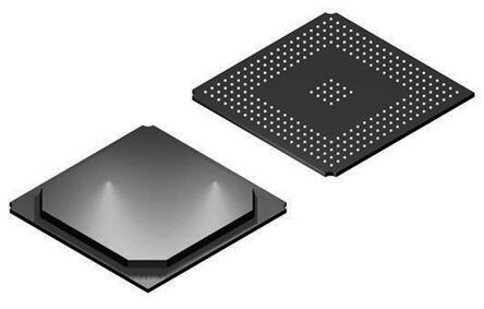
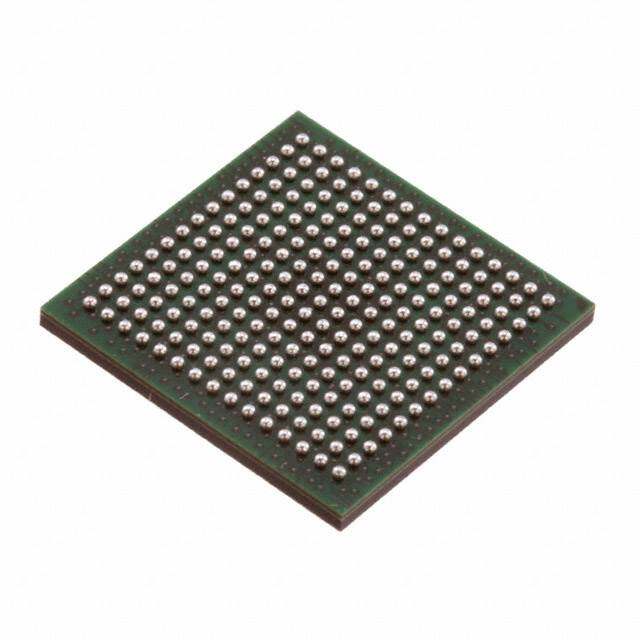
| 描述 | IC FLOATING-POINT DSP 272-BGA |
| 产品分类 | |
| 品牌 | Texas Instruments |
| 数据手册 | |
| 产品图片 |
|
| 产品型号 | TMS320C6713BGDP300 |
| PCN组件/产地 | |
| rohs | 含铅 / 不符合限制有害物质指令(RoHS)规范要求 |
| 产品系列 | TMS320C67x |
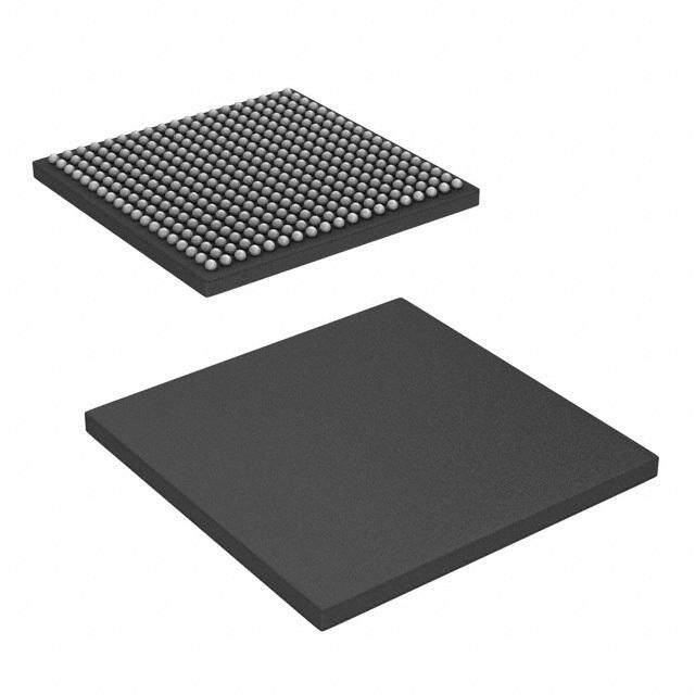
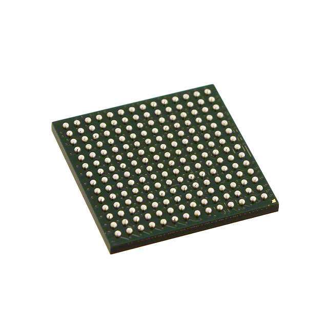
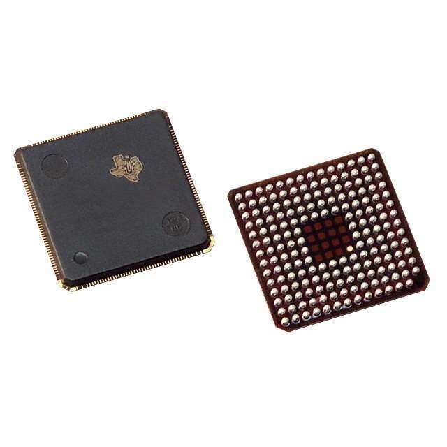
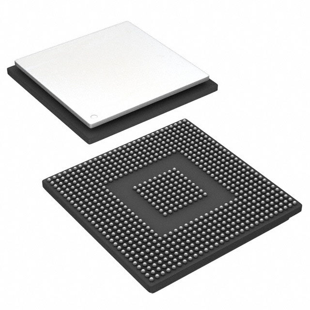
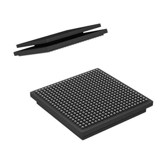
| 供应商器件封装 | 272-BGA(27x27) |
| 其它名称 | 296-17377 |
| 包装 | 托盘 |
| 安装类型 | 表面贴装 |
| 封装/外壳 | 272-BBGA |
| 工作温度 | 0°C ~ 90°C |
| 接口 | 主机接口,I²C,McASP,McBSP |
| 时钟速率 | 300MHz |
| 标准包装 | 40 |
| 片载RAM | 264kB |
| 电压-I/O | 3.30V |
| 电压-内核 | 1.40V |
| 类型 | 浮点 |
| 配用 | /product-detail/zh/TMDSDSK6713/296-15831-ND/592235/product-detail/zh/TMDSDSK6713-0E/296-23033-ND/1785979 |
| 非易失性存储器 | 外部 |


PDF Datasheet 数据手册内容提取
(cid:1)(cid:2)(cid:3)(cid:4)(cid:5)(cid:6)(cid:7)(cid:8)(cid:9)(cid:10)(cid:4)(cid:11) (cid:12)(cid:13)(cid:14)(cid:15)(cid:1)(cid:16)(cid:17)(cid:18)(cid:19)(cid:20)(cid:14)(cid:16)(cid:17)(cid:1) (cid:21)(cid:16)(cid:18)(cid:16)(cid:1)(cid:15)(cid:13) (cid:3)(cid:16)(cid:18)(cid:17)(cid:15)(cid:13) (cid:20)(cid:22)(cid:14)(cid:7)(cid:23)(cid:3)(cid:3)(cid:14)(cid:22) SPRS294B − OCTOBER 2005 − REVISED JUNE 2006 (cid:1) (cid:1) Highest-Performance Floating-Point Digital 16-Bit Host-Port Interface (HPI) Signal Processor (DSP): TMS320C6713B (cid:1) Two McASPs − Eight 32-Bit Instructions/Cycle − Two Independent Clock Zones Each − 32/64-Bit Data Word (1 TX and 1 RX) − 300-, 225-, 200-MHz (GDP and ZDP), and − Eight Serial Data Pins Per Port: 225-, 200-, 167-MHz (PYP) Clock Rates Individually Assignable to any of the − 3.3-, 4.4-, 5-, 6-Instruction Cycle Times Clock Zones − 2400/1800, 1800/1350, 1600/1200, and − Each Clock Zone Includes: 1336/1000 MIPS/MFLOPS − Programmable Clock Generator − Rich Peripheral Set, Optimized for Audio − Programmable Frame Sync Generator − Highly Optimized C/C++ Compiler − TDM Streams From 2-32 Time Slots − Extended Temperature Devices Available − Support for Slot Size: (cid:1) Advanced Very Long Instruction Word 8, 12, 16, 20, 24, 28, 32 Bits (VLIW) TMS320C67x DSP Core − Data Formatter for Bit Manipulation − Eight Independent Functional Units: − Wide Variety of I2S and Similar Bit − 2 ALUs (Fixed-Point) Stream Formats − 4 ALUs (Floating-/Fixed-Point) − Integrated Digital Audio Interface − 2 Multipliers (Floating-/Fixed-Point) Transmitter (DIT) Supports: − Load-Store Architecture With 32 32-Bit − S/PDIF, IEC60958-1, AES-3, CP-430 General-Purpose Registers Formats − Instruction Packing Reduces Code Size − Up to 16 transmit pins − All Instructions Conditional − Enhanced Channel Status/User Data (cid:1) Instruction Set Features − Extensive Error Checking and Recovery − Native Instructions for IEEE 754 (cid:1) Two Inter-Integrated Circuit Bus (I2C Bus) − Single- and Double-Precision Multi-Master and Slave Interfaces − Byte-Addressable (8-, 16-, 32-Bit Data) (cid:1) Two Multichannel Buffered Serial Ports: − 8-Bit Overflow Protection − Serial-Peripheral-Interface (SPI) − Saturation; Bit-Field Extract, Set, Clear; − High-Speed TDM Interface Bit-Counting; Normalization − AC97 Interface (cid:1) L1/L2 Memory Architecture (cid:1) Two 32-Bit General-Purpose Timers − 4K-Byte L1P Program Cache (cid:1) Dedicated GPIO Module With 16 pins (Direct-Mapped) (External Interrupt Capable) − 4K-Byte L1D Data Cache (2-Way) (cid:1) Flexible Phase-Locked-Loop (PLL) Based − 256K-Byte L2 Memory Total: 64K-Byte Clock Generator Module L2 Unified Cache/Mapped RAM, and 192K-Byte Additional L2 Mapped RAM (cid:1) IEEE-1149.1 (JTAG†) (cid:1) Boundary-Scan-Compatible Device Configuration − Boot Mode: HPI, 8-, 16-, 32-Bit ROM Boot (cid:1) 208-Pin PowerPAD PQFP (PYP) − Endianness: Little Endian, Big Endian (cid:1) 272-BGA Packages (GDP and ZDP) (cid:1) 32-Bit External Memory Interface (EMIF) (cid:1) 0.13-µm/6-Level Copper Metal Process − Glueless Interface to SRAM, EPROM, − CMOS Technology Flash, SBSRAM, and SDRAM (cid:1) 3.3-V I/Os, 1.2‡-V Internal (GDP/ZDP/ PYP) − 512M-Byte Total Addressable External (cid:1) 3.3-V I/Os, 1.4-V Internal (GDP/ZDP) [300 Memory Space (cid:1) MHz] Enhanced Direct-Memory-Access (EDMA) Controller (16 Independent Channels) Please be aware that an important notice concerning availability, standard warranty, and use in critical applications of TexasInstruments semiconductor products and disclaimers thereto appears at the end of this data sheet. TMS320C67x and PowerPAD are trademarks of Texas Instruments. I2C Bus is a trademark of Philips Electronics N.V. Corporation All trademarks are the property of their respective owners. †IEEE Standard 1149.1-1990 Standard-Test-Access Port and Boundary Scan Architecture. ‡These values are compatible with existing 1.26-V designs. (cid:20)(cid:22)(cid:14)(cid:21)(cid:24)(cid:7)(cid:1)(cid:16)(cid:14)(cid:17) (cid:21)(cid:15)(cid:1)(cid:15) (cid:25)(cid:26)(cid:27)(cid:28)(cid:29)(cid:30)(cid:31)!(cid:25)(cid:28)(cid:26) (cid:25)" #$(cid:29)(cid:29)%(cid:26)! (cid:31)" (cid:28)(cid:27) &$’((cid:25)#(cid:31)!(cid:25)(cid:28)(cid:26) )(cid:31)!%* Copyright 2006, Texas Instruments Incorporated (cid:20)(cid:29)(cid:28))$#!" #(cid:28)(cid:26)(cid:27)(cid:28)(cid:29)(cid:30) !(cid:28) "&%#(cid:25)(cid:27)(cid:25)#(cid:31)!(cid:25)(cid:28)(cid:26)" &%(cid:29) !+% !%(cid:29)(cid:30)" (cid:28)(cid:27) (cid:1)%,(cid:31)" (cid:16)(cid:26)"!(cid:29)$(cid:30)%(cid:26)!" "!(cid:31)(cid:26))(cid:31)(cid:29)) -(cid:31)(cid:29)(cid:29)(cid:31)(cid:26)!.* (cid:20)(cid:29)(cid:28))$#!(cid:25)(cid:28)(cid:26) &(cid:29)(cid:28)#%""(cid:25)(cid:26)/ )(cid:28)%" (cid:26)(cid:28)! (cid:26)%#%""(cid:31)(cid:29)(cid:25)(. (cid:25)(cid:26)#($)% !%"!(cid:25)(cid:26)/ (cid:28)(cid:27) (cid:31)(( &(cid:31)(cid:29)(cid:31)(cid:30)%!%(cid:29)"* POST OFFICE BOX 1443 • HOUSTON, TEXAS 77251−1443 1
(cid:1)(cid:2)(cid:3)(cid:4)(cid:5)(cid:6)(cid:7)(cid:8)(cid:9)(cid:10)(cid:4)(cid:11) (cid:12)(cid:13)(cid:14)(cid:15)(cid:1)(cid:16)(cid:17)(cid:18)(cid:19)(cid:20)(cid:14)(cid:16)(cid:17)(cid:1) (cid:21)(cid:16)(cid:18)(cid:16)(cid:1)(cid:15)(cid:13) (cid:3)(cid:16)(cid:18)(cid:17)(cid:15)(cid:13) (cid:20)(cid:22)(cid:14)(cid:7)(cid:23)(cid:3)(cid:3)(cid:14)(cid:22) SPRS294B − OCTOBER 2005 − REVISED JUNE 2006 Table of Contents revision history . . . . . . . . . . . . . . . . . . . . . . . . . . . . . . . . . . . . . . 3 EMIF device speed . . . . . . . . . . . . . . . . . . . . . . . . . . . . . . 95 GDP and ZDP 272-Ball BGA package (bottom view) . . . . . 5 EMIF big endian mode correctness . . . . . . . . . . . . . . . . 97 PYP PowerPAD QFP package (top view) . . . . . . . . . . . . 10 bootmode . . . . . . . . . . . . . . . . . . . . . . . . . . . . . . . . . . . . . . 98 description . . . . . . . . . . . . . . . . . . . . . . . . . . . . . . . . . . . . . . . . 11 reset. . . . . . . . . . . . . . . . . . . . . . . . . . . . . . . . . . . . . . . . . . . 98 device characteristics . . . . . . . . . . . . . . . . . . . . . . . . . . . . . . . 12 absolute maximum ratings over operating case temperature range . . . . . . . . . . . . . . . . . . . . . . . . . . 99 functional block and CPU (DSP core) diagram. . . . . . . . . . 13 recommended operating conditions . . . . . . . . . . . . . . . . 99 CPU (DSP core) description . . . . . . . . . . . . . . . . . . . . . . . . . 14 electrical characteristics over recommended ranges of memory map summary. . . . . . . . . . . . . . . . . . . . . . . . . . . . . . 16 supply voltage and operating case temperature 100 peripheral register descriptions . . . . . . . . . . . . . . . . . . . . . . . 18 parameter measurement information . . . . . . . . . . . . . . 101 signal groups description . . . . . . . . . . . . . . . . . . . . . . . . . . . . 27 signal transition levels. . . . . . . . . . . . . . . . . . . . . . . . . . . 101 device configurations . . . . . . . . . . . . . . . . . . . . . . . . . . . . . . . 32 timing parameters and board routing analysis . . . . . . 103 configuration examples. . . . . . . . . . . . . . . . . . . . . . . . . . . . . . 40 input and output clocks. . . . . . . . . . . . . . . . . . . . . . . . . . 105 debugging considerations . . . . . . . . . . . . . . . . . . . . . . . . . . . 47 asynchronous memory timing . . . . . . . . . . . . . . . . . . . . 108 terminal functions . . . . . . . . . . . . . . . . . . . . . . . . . . . . . . . . . . 48 synchronous-burst memory timing . . . . . . . . . . . . . . . . . 111 development support. . . . . . . . . . . . . . . . . . . . . . . . . . . . . . . . 64 synchronous DRAM timing. . . . . . . . . . . . . . . . . . . . . . . 113 device support . . . . . . . . . . . . . . . . . . . . . . . . . . . . . . . . . . . . . 65 HOLD/HOLDA timing . . . . . . . . . . . . . . . . . . . . . . . . . . . 119 CPU CSR register description . . . . . . . . . . . . . . . . . . . . . . . . 68 BUSREQ timing . . . . . . . . . . . . . . . . . . . . . . . . . . . . . . . . 120 cache configuration (CCFG) register description . . . . . . . . 70 reset timing . . . . . . . . . . . . . . . . . . . . . . . . . . . . . . . . . . . . 121 interrupts and interrupt selector. . . . . . . . . . . . . . . . . . . . . . . 71 external interrupt timing . . . . . . . . . . . . . . . . . . . . . . . . . 123 external interrupt sources. . . . . . . . . . . . . . . . . . . . . . . . . . . . 73 multichannel audio serial port (McASP) timing . . . . . . 124 EDMA module and EDMA selector. . . . . . . . . . . . . . . . . . . . 74 inter-integrated circuits (I2C) timing . . . . . . . . . . . . . . . 127 PLL and PLL controller . . . . . . . . . . . . . . . . . . . . . . . . . . . . . . 77 host-port interface timing . . . . . . . . . . . . . . . . . . . . . . . . 129 multichannel audio serial port (McASP) peripherals . . . . . 84 multichannel buffered serial port timing . . . . . . . . . . . . 132 I2C . . . . . . . . . . . . . . . . . . . . . . . . . . . . . . . . . . . . . . . . . . . . . . . 89 timer timing . . . . . . . . . . . . . . . . . . . . . . . . . . . . . . . . . . . . 142 general-purpose input/output (GPIO) . . . . . . . . . . . . . . . . . . 90 general-purpose input/output (GPIO) port timing . . . . 143 power-down mode logic . . . . . . . . . . . . . . . . . . . . . . . . . . . . . 91 JTAG test-port timing . . . . . . . . . . . . . . . . . . . . . . . . . . . 144 power-supply sequencing. . . . . . . . . . . . . . . . . . . . . . . . . . . . 93 mechanical data. . . . . . . . . . . . . . . . . . . . . . . . . . . . . . . . 145 IEEE 1149.1 JTAG compatibility statement . . . . . . . . . . . . . 95 power-supply decoupling . . . . . . . . . . . . . . . . . . . . . . . . . . . . 94 2 POST OFFICE BOX 1443 • HOUSTON, TEXAS 77251−1443
(cid:1)(cid:2)(cid:3)(cid:4)(cid:5)(cid:6)(cid:7)(cid:8)(cid:9)(cid:10)(cid:4)(cid:11) (cid:12)(cid:13)(cid:14)(cid:15)(cid:1)(cid:16)(cid:17)(cid:18)(cid:19)(cid:20)(cid:14)(cid:16)(cid:17)(cid:1) (cid:21)(cid:16)(cid:18)(cid:16)(cid:1)(cid:15)(cid:13) (cid:3)(cid:16)(cid:18)(cid:17)(cid:15)(cid:13) (cid:20)(cid:22)(cid:14)(cid:7)(cid:23)(cid:3)(cid:3)(cid:14)(cid:22) SPRS294B − OCTOBER 2005 − REVISED JUNE 2006 REVISION HISTORY The TMS320C6713B device-specific documentation has been split from TMS320C6713, TMS320C6713B Float- ing−Point Digital Signal Processors, literature number SPRS186K, into a separate Data Sheet, literature number SPRS294. It also highlights technical changes made to SPRS294 to generate SPRS294A. These changes are marked by “[Revision A].” Additionally, made changes to SPRS294A to generate SPRS294B. These changes are marked by “[Revision B].” Both Revision A and B changes are noted in the Revision History table below. Scope: Updated information on McASP, McBSP and JTAG for clarification. Changed Pin Description for A12 and B11 (Revisions SPRS294 and SPRS294A). Updated Nomenclature figure by adding device−specific information for the ZDP package. TI Recommends for new designs that the following pins be configured as such: (cid:1) Pin A12 connected directly to CV (core power) DD (cid:1) Pin B11 connected directly to V (ground) ss PAGE(S) ADDITIONS/CHANGES/DELETIONS NO. 6 Terminal Assignments for the 272-Ball GDP and ZDP Packages (in Order of Ball No.) table: Updated Signal Name for Ball No. A12 Updated Signal Name for Ball No. B11 10 PYP PowerPAD QFP package (top view): Updated drawing 32 Device Configurations, device configurations at device reset section: Updated “For proper device operation...” paragraph [Revision B] 33 Device Configurations, Device Configurations Pins at Device Reset (HD[4:3], HD8, HD12, and CLKMODE0) section: Removed “CE1 width 32−bit” from Functional Description for “00” in HD[4:3](BOOTMODE) Configuration Pin 33 Device Configurations, Device Configurations Pins at Device Reset (HD[4:3], HD8, HD12, and CLKMODE0) section: Updated “All other HD pins...” footnote [Revision B] 37 Table 22 Peripheral Pin Selection Matrix: Updated/changed MCBSP0DIS (DEVCFG bit) from “ACLKKO” to “ACLKXO” 46 Configuration Example F (1 McBSP + HPI + 1 McASP) figure: Updated from McBSP1DIS = 1 to McBSP1DIS = 0 47 Device Configurations, debugging considerations section: Updated “Internal pullup/pulldown resistors...” paragraph [Revision B] 49 Terminal Functions, Resets and Interrupts section: Updated IPU/IPD for RESET Signal Name from “IPU” to “−−” 50 Terminal Functions table, Host Port Interface section: Removed “CE1 width 32−bit” from Description for “00” in Bootmode HD[4:3] 50 Terminal Functions table, Host Port Interface section: Updated “Other HD pins...” paragraph [Revision B] 55 Terminal Functions, Timer 1 section: Updated Description for TINP1/AHCLKX0 Signal Name 57 Terminal Functions, Reserved for Test section: Updated Description for RSV Signal Name, 181 PYP, A12 GDP/ZDP Updated Description for RSV Signal Name, 180 PYP, B11 GDP/ZDP POST OFFICE BOX 1443 • HOUSTON, TEXAS 77251−1443 3
(cid:1)(cid:2)(cid:3)(cid:4)(cid:5)(cid:6)(cid:7)(cid:8)(cid:9)(cid:10)(cid:4)(cid:11) (cid:12)(cid:13)(cid:14)(cid:15)(cid:1)(cid:16)(cid:17)(cid:18)(cid:19)(cid:20)(cid:14)(cid:16)(cid:17)(cid:1) (cid:21)(cid:16)(cid:18)(cid:16)(cid:1)(cid:15)(cid:13) (cid:3)(cid:16)(cid:18)(cid:17)(cid:15)(cid:13) (cid:20)(cid:22)(cid:14)(cid:7)(cid:23)(cid:3)(cid:3)(cid:14)(cid:22) SPRS294B − OCTOBER 2005 − REVISED JUNE 2006 PAGE(S) ADDITIONS/CHANGES/DELETIONS NO. 57 Terminal Functions, Reserved for Test section: Updated/changed Description for RSV Signal Name, A12 GDP (to “recommended”) − [Revision A] Updated/changed Description for RSV Signal Name, B11 GDP (to “recommended”) − [Revision A] 57 Terminal Functions, Reserved for Test section: Updated/changed Description for RSV Signal Name D12 to include PYP 178 as follows: “...the D12/178 pin must be externally pulled down with a 10−kΩ resistor.” [Revision B] 66 Device Support, device and development-support tool nomenclature section: Updated figure for clarity 67 Device Support, document support section: Updated paragraphs for clarity 92 Power−Down Mode Logic − Triggering, Wake−up and Effects section: Updated paragraphs [Revision B] 93 Power−Down Mode Logic − Triggering, Wake−up and Effects section, Characteristics of the Power-Down Modes table: Added “It is recommended to use the PLLPWDN bit (PLLCSR.1) as an alternative to PD3” to PRWD Field (BITS 15−10) − 011100 − Effect on Chip’s Operation [Revision B] 93 Power−Down Mode Logic − Triggering, Wake−up and Effects section, Characteristics of the Power-Down Modes table: Deleted three paragraphs following table [Revision B] 95 IEEE 1149.1 JTAG Compatibility Statement section: Updated/added paragraphs for clarity 96 EMIF Device Speed section, Example Boards and Maximum EMIF Speed table: Type − 3−Loads Short Traces, EMIF Interface Components section: Updated from “32−Bit SDRAMs” to “16−Bit SDRAMs” [Revision B] 95 IEEE 1149.1 JTAG Compatibility Statement section: Updated/added paragraphs for clarity 99 Recommended Operating Conditions: Added VOS, Maximum voltage during overshoot row and associated footnote Added VUS, Maximum voltage during undershoot row and associated footnote 102 Parameter Measurement Information, AC transient rise/fall time specifications section: Added AC Transient Specification Rise Time figure Added AC Transient Specification Fall Time figure 124 MULTICHANNEL AUDIO SERIAL PORT (McASP) TIMING: timing requirements for McASP section: Updated Parameter No. 3, tc(ACKRX), from “33” to “greater of 2P or 33 ns” and added associated footnote 124 MULTICHANNEL AUDIO SERIAL PORT (McASP) TIMING: switching characteristics over recommended operating conditions for McASP section: Updated Parameter No. 11, tc(ACKRX), from “33” to “greater of 2P or 33 ns” and added associated footnote 125, 126 MULTICHANNEL AUDIO SERIAL PORT (McASP) TIMING section: Updated McASP Input and Output drawings 134 MULTICHANNEL BUFFERED SERIAL PORT TIMING section: switching characteristics over recommended operating conditions for McBSP section: Updated McBSP Timings figure 147 Mechanical Data section: Added statement to the Packaging Information section 4 POST OFFICE BOX 1443 • HOUSTON, TEXAS 77251−1443
(cid:1)(cid:2)(cid:3)(cid:4)(cid:5)(cid:6)(cid:7)(cid:8)(cid:9)(cid:10)(cid:4)(cid:11) (cid:12)(cid:13)(cid:14)(cid:15)(cid:1)(cid:16)(cid:17)(cid:18)(cid:19)(cid:20)(cid:14)(cid:16)(cid:17)(cid:1) (cid:21)(cid:16)(cid:18)(cid:16)(cid:1)(cid:15)(cid:13) (cid:3)(cid:16)(cid:18)(cid:17)(cid:15)(cid:13) (cid:20)(cid:22)(cid:14)(cid:7)(cid:23)(cid:3)(cid:3)(cid:14)(cid:22) SPRS294B − OCTOBER 2005 − REVISED JUNE 2006 GDP and ZDP 272-Ball BGA package (bottom view) > 0(cid:3)(cid:3) 0(cid:3)(cid:3) (cid:23)(cid:21)(cid:10)< (cid:11)(cid:23)(cid:5) (cid:15)(cid:22)(cid:21)> (cid:23)(cid:15)(cid:5) (cid:21)0(cid:21)(cid:21) (cid:23)(cid:15)(cid:9) (cid:23)(cid:15)4 (cid:23)(cid:7)(cid:13)1(cid:14)(cid:24)(cid:1) (cid:23)(cid:7)(cid:13)1(cid:16)(cid:17) (cid:7)(cid:13)(cid:18)1(cid:20)(cid:14)5(cid:24)(cid:5)6(cid:1)(cid:5); 0(cid:3)(cid:3) (cid:23)(cid:15)(cid:10)2 (cid:23)(cid:15)(cid:10)(cid:8) (cid:23)(cid:15)(cid:10)< (cid:21)0(cid:21)(cid:21) (cid:23)(cid:15)(cid:5)(cid:6) 0(cid:3)(cid:3) 0(cid:3)(cid:3) (cid:15)(cid:14)(cid:23); ? 0(cid:3)(cid:3) (cid:7)0(cid:21)(cid:21) (cid:21)0(cid:21)(cid:21) (cid:23)(cid:21)(cid:10)(cid:9) 0(cid:3)(cid:3) (cid:7)(cid:23)(cid:5) (cid:23)(cid:15)2 (cid:23)(cid:15)(cid:8) (cid:21)0(cid:21)(cid:21) (cid:3)(cid:3)(cid:21)(cid:3)(cid:22)(cid:14)(cid:15)(cid:23)(cid:3); 0(cid:3)(cid:3) (cid:21)0(cid:21)(cid:21) (cid:23)(cid:15)(cid:10)(cid:10) (cid:23)(cid:15)(cid:10)(cid:4) (cid:23)(cid:15)(cid:10)3 0(cid:3)(cid:3) (cid:23)(cid:15)(cid:10)4 (cid:7)(cid:23)(cid:10) (cid:7)0(cid:21)(cid:21) 0(cid:3)(cid:3) (cid:15)(cid:22)(cid:23); (cid:15)?(cid:23); 0 (cid:23)(cid:21)(cid:5)(cid:6) (cid:23)(cid:21)(cid:10)4 (cid:7)0(cid:21)(cid:21) (cid:23)(cid:21)(cid:10)(cid:8) (cid:11)(cid:23)(cid:4) (cid:7)(cid:23)(cid:4) (cid:23)(cid:15)(cid:4) (cid:23)(cid:15)3 (cid:23)(cid:15)< (cid:23)(cid:15)(cid:10)(cid:6) (cid:3)(cid:3)(cid:21)(cid:3)(cid:7)(cid:15)(cid:15)(cid:21)(cid:3)(cid:3); (cid:3)(cid:3)(cid:21)(cid:3)??(cid:23)(cid:23); (cid:21)0(cid:21)(cid:21) (cid:23)(cid:15)(cid:10)(cid:5) (cid:21)0(cid:21)(cid:21) (cid:23)(cid:15)(cid:10)(cid:9) (cid:7)(cid:23)(cid:6) (cid:7)0(cid:21)(cid:21) (cid:21)0(cid:21)(cid:21) (cid:11)(cid:23)(cid:6) (cid:24) (cid:23)(cid:21)(cid:5)(cid:5) (cid:23)(cid:21)(cid:5)(cid:10) (cid:23)(cid:21)(cid:5)(cid:4) 0(cid:3)(cid:3) (cid:21)0(cid:21)(cid:21) (cid:7)0(cid:21)(cid:21) (cid:21)0(cid:21)(cid:21) 0(cid:3)(cid:3) 0(cid:3)(cid:3) (cid:7)0(cid:21)(cid:21) (cid:7)0(cid:21)(cid:21) (cid:21)0(cid:21)(cid:21) 0(cid:3)(cid:3) (cid:7)0(cid:21)(cid:21) (cid:7)0(cid:21)(cid:21) (cid:21)0(cid:21)(cid:21) 0(cid:3)(cid:3) (cid:23)(cid:15)(cid:5)(cid:10) (cid:11)(cid:23)(cid:10) 0(cid:3)(cid:3) (cid:1) (cid:23)(cid:21)(cid:5)2 (cid:23)(cid:21)(cid:5)3 (cid:21)0(cid:21)(cid:21) 0(cid:3)(cid:3) 0(cid:3)(cid:3) (cid:23)(cid:21)(cid:10)(cid:4) (cid:23)(cid:21)(cid:10)3 (cid:23)(cid:21)(cid:10)2 (cid:22) (cid:21)0(cid:21)(cid:21) (cid:23)(cid:21)(cid:5)(cid:9) (cid:23)(cid:21)(cid:5)(cid:8) (cid:7)0(cid:21)(cid:21) (cid:7)0(cid:21)(cid:21) (cid:21)0(cid:21)(cid:21) (cid:23)(cid:21)(cid:10)(cid:10) (cid:23)(cid:21)(cid:10)(cid:5) (cid:20) (cid:23)(cid:21)(cid:5)< (cid:23)(cid:21)(cid:5)4 (cid:23)(cid:21)(cid:4)(cid:6) 0(cid:3)(cid:3) 0(cid:3)(cid:3) (cid:23)(cid:21)4 0(cid:3)(cid:3) (cid:23)(cid:21)(cid:10)(cid:6) (cid:17) (cid:3)(cid:7)(cid:13)(cid:6) (cid:3)(cid:21)(cid:15)(cid:6) (cid:23)(cid:21)(cid:4)(cid:10) 0(cid:3)(cid:3) 0(cid:3)(cid:3) (cid:23)(cid:21)(cid:8) (cid:23)(cid:21)(cid:9) (cid:23)(cid:21)< (cid:2) (cid:15)(cid:7)8(cid:13)(cid:22)1(cid:6)(cid:22)5(cid:10)(cid:8);6 (cid:3)(cid:21)(cid:21)(cid:22)(cid:15)(cid:10)(cid:10); (cid:15)(cid:12)8(cid:3)(cid:22)(cid:22)(cid:6)(cid:10)5(cid:9);6 0(cid:3)(cid:3) 0(cid:3)(cid:3) 0(cid:3)(cid:3) 0(cid:3)(cid:3) 0(cid:3)(cid:3) 0(cid:3)(cid:3) (cid:21)0(cid:21)(cid:21) (cid:23)(cid:21)2 (cid:23)(cid:21)3 (cid:13) (cid:12)(cid:3)8(cid:10) (cid:15)8(cid:21)(cid:22)8(cid:6)(cid:10)5;36 (cid:15)(cid:7)(cid:2)(cid:13)(cid:24)1(cid:1)8(cid:23)(cid:10);(cid:6) (cid:7)0(cid:21)(cid:21) 0(cid:3)(cid:3) 0(cid:3)(cid:3) 0(cid:3)(cid:3) 0(cid:3)(cid:3) (cid:7)0(cid:21)(cid:21) (cid:23)(cid:21)(cid:5) (cid:23)(cid:21)(cid:4) (cid:7)0(cid:21)(cid:21) 1 (cid:7)0(cid:21)(cid:21) 0(cid:3)(cid:3) (cid:15)(cid:7)=(cid:13)(cid:7)1(cid:13)(cid:3)1(cid:6)(cid:22);(cid:6) (cid:7)0(cid:21)(cid:21) 0(cid:3)(cid:3) 0(cid:3)(cid:3) 0(cid:3)(cid:3) 0(cid:3)(cid:3) (cid:7)0(cid:21)(cid:21) (cid:23)(cid:21)(cid:6) (cid:23)(cid:21)(cid:10) 0(cid:3)(cid:3) @ (cid:15)8(cid:21)(cid:22)(cid:22)(cid:6)(cid:6)5;(cid:6)6 (cid:21)0(cid:21)(cid:21) (cid:15)(cid:12)(cid:12)(cid:3)(cid:3)(cid:22)(cid:22)(cid:6)(cid:6); 0(cid:3)(cid:3) 0(cid:3)(cid:3) 0(cid:3)(cid:3) 0(cid:3)(cid:3) 0(cid:3)(cid:3) =(cid:14)(cid:13)(cid:21) =(cid:14)(cid:13)(cid:21)(cid:15) (cid:22)(cid:11)(cid:23)(cid:24)A(cid:3) (cid:18)=(cid:16)(cid:20)(cid:17)5(cid:1)(cid:10)6; = (cid:15)(cid:12)(cid:12)(cid:3)(cid:3)88(cid:6)(cid:6); (cid:15)8(cid:21)(cid:22)8(cid:6)(cid:6)5;(cid:10)6 (cid:15)(cid:7)(cid:7)(cid:13)(cid:13)11(cid:22)(cid:22)(cid:6)(cid:6); 0(cid:3)(cid:3) 0(cid:3)(cid:3) (cid:21)0(cid:21)(cid:21) (cid:15)=(cid:7)(cid:22)(cid:13)(cid:21)1>(cid:22);(cid:10) =(cid:15)=(cid:12)?(cid:3)(cid:22)(cid:16)(cid:13)(cid:10); (cid:18) (cid:15)(cid:1)8(cid:14)(cid:22)(cid:24)(cid:6)(cid:1)5(cid:6)(cid:5);6 (cid:15)(cid:1)8(cid:16)(cid:17)(cid:22)(cid:20)(cid:6)5(cid:6)(cid:4);6 (cid:15)(cid:7)(cid:7)(cid:13)(cid:13)1188(cid:6)(cid:6); 0(cid:3)(cid:3) 0(cid:3)(cid:3) =(cid:7)(cid:17)(cid:1)(cid:13)(cid:6); =(cid:7)(cid:17)(cid:1)(cid:13)(cid:10); =(cid:22);?; (cid:15)8(cid:22)(cid:10)5(cid:4)6 (cid:15)8(cid:22)(cid:10)5(cid:10)6 (cid:15)8(cid:22)(cid:10)5(cid:6)6 (cid:12) (cid:15)(cid:1)8(cid:14)(cid:22)(cid:24)(cid:6)(cid:1)5(cid:10)2;6 (cid:15)=(cid:1)(cid:16)(cid:7)(cid:17)(cid:13)(cid:20)1(cid:10)8;(cid:6) (cid:21)0(cid:21)(cid:21) (cid:7)0(cid:21)(cid:21) (cid:7)0(cid:21)(cid:21) (cid:15)=8(cid:21)(cid:22)(cid:3)(cid:10)(cid:5)53;6 0(cid:3)(cid:3) (cid:15)8=(cid:22)(cid:7)(cid:10)(cid:3)5;(cid:5)6 (cid:23) (cid:7)(cid:3)(cid:13)(cid:7)1(cid:13)(cid:3)(cid:10)(cid:10); 0(cid:3)(cid:3) 7(cid:23)8(cid:18)(cid:1)(cid:20)95(cid:16)(cid:9)(cid:17)6(cid:1)(cid:9): 0(cid:3)(cid:3) 0(cid:3)(cid:3) (cid:15)(cid:7)=(cid:13)(cid:15)1(cid:3)8;(cid:10) (cid:15)=8(cid:21)(cid:22)(cid:3)(cid:10)(cid:10)5(cid:8);6 (cid:15)8=(cid:22)(cid:21)(cid:10)(cid:6)5;26 (cid:21) (cid:21)0(cid:21)(cid:21) 7(cid:23)8(cid:18)(cid:1)(cid:20)95(cid:16)(cid:8)(cid:17)6(cid:1)(cid:8): (cid:23)(cid:2)(cid:24)(cid:5) 0(cid:3)(cid:3) (cid:7)0(cid:21)(cid:21) (cid:7)0(cid:21)(cid:21) (cid:22)(cid:3)0 0(cid:3)(cid:3) (cid:23)(cid:2)(cid:24)(cid:6) (cid:7)(cid:13)1(cid:14)(cid:24)(cid:1)(cid:4) (cid:7)0(cid:21)(cid:21) (cid:22)(cid:3)0 0(cid:3)(cid:3) (cid:7)0(cid:21)(cid:21) (cid:7)0(cid:21)(cid:21) (cid:21)0(cid:21)(cid:21) 0(cid:3)(cid:3) (cid:15)=(cid:12)(cid:21)(cid:3)(cid:5)8;(cid:10) (cid:21)0(cid:21)(cid:21) (cid:15)8=(cid:22)(cid:21)(cid:10)(cid:10)5;(cid:9)6 (cid:7)7(cid:15)(cid:23)(cid:2)8(cid:18)(cid:1)(cid:24)(cid:20)9(cid:1)(cid:16)5(cid:17)(cid:23)36(cid:16)(cid:1)(cid:17)3(cid:6):;7(cid:15)(cid:23)(cid:2)8(cid:18)(cid:1)(cid:24)(cid:20)9(cid:1)5(cid:16)2(cid:17)(cid:23)6(cid:16)(cid:1);(cid:17)2(cid:10):; (cid:7)0(cid:21)(cid:21) (cid:2)(cid:7)(cid:14)(cid:13)(cid:21)1(cid:23)(cid:6) (cid:20)(cid:13)(cid:13)=0 0(cid:3)(cid:3) (cid:7)0(cid:21)(cid:21) 0(cid:3)(cid:3) 0(cid:3)(cid:3) (cid:21)0(cid:21)(cid:21) (cid:23)(cid:2)(cid:24)2 (cid:22)(cid:3)0 (cid:17)(cid:2)(cid:16) (cid:18)=(cid:20)(cid:21)5(cid:10)(cid:10)22;6 (cid:18)=(cid:20)(cid:21)5(cid:10)(cid:10)(cid:5)(cid:5);6 (cid:18)=(cid:20)(cid:21)544;6 (cid:15)==(cid:7)(cid:21)(cid:13)(cid:8)1;(cid:22)(cid:10) (cid:7)0(cid:21)(cid:21) (cid:18)=(cid:20)(cid:21)52(cid:6);6 (cid:15)(cid:2)=(cid:24)(cid:21)(cid:1)(cid:4)(cid:23);(cid:10) (cid:11) 0(cid:3)(cid:3) (cid:7)0(cid:21)(cid:21) (cid:21)0(cid:21)(cid:21) 0(cid:3)(cid:3) (cid:22)(cid:3)0 (cid:1)(cid:22)(cid:3)(cid:1) (cid:1)(cid:2)(cid:3) (cid:21)0(cid:21)(cid:21) (cid:23)(cid:2)(cid:24)(cid:10) (cid:23)(cid:2)(cid:24)(cid:4) (cid:22)(cid:3)0 (cid:23)(cid:2)(cid:24)3 (cid:21)0(cid:21)(cid:21) (cid:18)=(cid:20)(cid:21)5(cid:10)(cid:10)33;6 0(cid:3)(cid:3) (cid:18)=(cid:20)(cid:21)5(cid:10)(cid:10)(cid:6)(cid:6);6 (cid:18)=(cid:20)(cid:21)5<<;6 (cid:15)==(cid:7)(cid:21)(cid:13)31;8(cid:10) (cid:7)0(cid:21)(cid:21) 0(cid:3)(cid:3) =(cid:21)(cid:10)(cid:4); =(cid:21)(cid:10)(cid:10); (cid:15) 0(cid:3)(cid:3) 0(cid:3)(cid:3) (cid:7)(cid:13)1(cid:16)(cid:17) (cid:7)0(cid:21)(cid:21) (cid:22)(cid:3)0 (cid:1)(cid:7)1 (cid:1)(cid:21)(cid:16) (cid:1)(cid:21)(cid:14) (cid:7)0(cid:21)(cid:21) (cid:7)0(cid:21)(cid:21) 0(cid:3)(cid:3) (cid:22)(cid:3)0 (cid:22)(cid:23)(cid:3)(cid:23)(cid:1) 0(cid:3)(cid:3) (cid:18)(cid:20)5(cid:10)(cid:4)6 (cid:18)(cid:20)5(cid:10)(cid:10)6 (cid:21)0(cid:21)(cid:21) (cid:18)=(cid:20)(cid:21)5(cid:9)(cid:4);6 0(cid:3)(cid:3) 0(cid:3)(cid:3) (cid:10) (cid:5) (cid:4) 2 3 (cid:8) (cid:9) < 4 (cid:10)(cid:6) (cid:10)(cid:10) (cid:10)(cid:5) (cid:10)(cid:4) (cid:10)2 (cid:10)3 (cid:10)(cid:8) (cid:10)(cid:9) (cid:10)< (cid:10)4 (cid:5)(cid:6) (cid:1)(cid:2)(cid:3)(cid:4)(cid:5)(cid:6)(cid:7) (cid:4)(cid:8)(cid:6)(cid:9)(cid:10)(cid:8)(cid:11) (cid:10)(cid:2)(cid:8) (cid:12)(cid:13)(cid:14) (cid:15)(cid:3)(cid:16)(cid:17)(cid:3)(cid:7)(cid:8) (cid:15)(cid:5)(cid:6) (cid:18)(cid:19)(cid:6)(cid:16)(cid:10)(cid:5)(cid:9)(cid:6)(cid:11) (cid:10)(cid:2)(cid:3)(cid:10) (cid:4)(cid:20)(cid:9)(cid:15) (cid:9)(cid:19)(cid:10) (cid:9)(cid:6) (cid:10)(cid:2)(cid:8) (cid:14)(cid:21)(cid:14) (cid:15)(cid:3)(cid:16)(cid:17)(cid:3)(cid:7)(cid:8)(cid:22) POST OFFICE BOX 1443 • HOUSTON, TEXAS 77251−1443 5
(cid:1)(cid:2)(cid:3)(cid:4)(cid:5)(cid:6)(cid:7)(cid:8)(cid:9)(cid:10)(cid:4)(cid:11) (cid:12)(cid:13)(cid:14)(cid:15)(cid:1)(cid:16)(cid:17)(cid:18)(cid:19)(cid:20)(cid:14)(cid:16)(cid:17)(cid:1) (cid:21)(cid:16)(cid:18)(cid:16)(cid:1)(cid:15)(cid:13) (cid:3)(cid:16)(cid:18)(cid:17)(cid:15)(cid:13) (cid:20)(cid:22)(cid:14)(cid:7)(cid:23)(cid:3)(cid:3)(cid:14)(cid:22) SPRS294B − OCTOBER 2005 − REVISED JUNE 2006 Table 1. Terminal Assignments for the 272-Ball GDP and ZDP Packages (in Order of Ball No.) BALL NO. SIGNAL NAME BALL NO. SIGNAL NAME A1 VSS C1 GP[5](EXT_INT5)/AMUTEIN0 A2 VSS C2 GP[4](EXT_INT4)/AMUTEIN1 A3 CLKIN C3 CVDD A4 CVDD C4 CLKMODE0 A5 RSV C5 PLLHV A6 TCK C6 VSS A7 TDI C7 CVDD A8 TDO C8 VSS A9 CVDD C9 VSS A10 CVDD C10 DVDD A11 VSS C11 EMU4 A12 RSV [connect directly to CVDD] C12 RSV A13 RESET C13 NMI A14 VSS C14 HD14/GP[14] A15 HD13/GP[13] C15 HD12/GP[12] A16 HD11/GP[11] C16 HD9/GP[9] A17 DVDD C17 HD6/AHCLKR1 A18 HD7/GP[3] C18 CVDD A19 VSS C19 HD4/GP[0] A20 VSS C20 HD3/AMUTE1 B1 VSS D1 DVDD B2 CVDD D2 GP[6](EXT_INT6) B3 DVDD D3 EMU2 B4 VSS D4 VSS B5 RSV D5 CVDD B6 TRST D6 CVDD B7 TMS D7 RSV B8 DVDD D8 VSS B9 EMU1 D9 EMU0 B10 EMU3 D10 CLKOUT3 B11 RSV [connect directly to VSS] D11 CVDD B12 EMU5 D12 RSV B13 DVDD D13 VSS B14 HD15/GP[15] D14 CVDD B15 VSS D15 CVDD B16 HD10/GP[10] D16 DVDD B17 HD8/GP[8] D17 VSS B18 HD5/AHCLKX1 D18 HD2/AFSX1 B19 CVDD D19 DVDD B20 VSS D20 HD1/AXR1[7] Shading denotes the GDP and ZDP package pin functions that drop out on the PYP package. 6 POST OFFICE BOX 1443 • HOUSTON, TEXAS 77251−1443
(cid:1)(cid:2)(cid:3)(cid:4)(cid:5)(cid:6)(cid:7)(cid:8)(cid:9)(cid:10)(cid:4)(cid:11) (cid:12)(cid:13)(cid:14)(cid:15)(cid:1)(cid:16)(cid:17)(cid:18)(cid:19)(cid:20)(cid:14)(cid:16)(cid:17)(cid:1) (cid:21)(cid:16)(cid:18)(cid:16)(cid:1)(cid:15)(cid:13) (cid:3)(cid:16)(cid:18)(cid:17)(cid:15)(cid:13) (cid:20)(cid:22)(cid:14)(cid:7)(cid:23)(cid:3)(cid:3)(cid:14)(cid:22) SPRS294B − OCTOBER 2005 − REVISED JUNE 2006 Table 1. Terminal Assignments for the 272-Ball GDP and ZDP Package (in Order of Ball No.) (Continued) BALL NO. SIGNAL NAME BALL NO. SIGNAL NAME E1 CLKS1/SCL1 J17 HOLD E2 VSS J18 HOLDA E3 GP[7](EXT_INT7) J19 BUSREQ E4 VSS J20 HINT/GP[1] E17 VSS K1 CVDD E18 HAS/ACLKX1 K2 VSS E19 HDS1/AXR1[6] K3 CLKS0/AHCLKR0 E20 HD0/AXR1[4] K4 CVDD F1 TOUT1/AXR0[4] K9 VSS F2 TINP1/AHCLKX0 K10 VSS F3 DVDD K11 VSS F4 CVDD K12 VSS F17 CVDD K17 CVDD F18 HDS2/AXR1[5] K18 ED0 F19 VSS K19 ED1 F20 HCS/AXR1[2] K20 VSS G1 TOUT0/AXR0[2] L1 FSX1 G2 TINP0/AXR0[3] L2 DX1/AXR0[5] G3 CLKX0/ACLKX0 L3 CLKX1/AMUTE0 G4 VSS L4 CVDD G17 VSS L9 VSS G18 HCNTL0/AXR1[3] L10 VSS G19 HCNTL1/AXR1[1] L11 VSS G20 HR/W/AXR1[0] L12 VSS H1 FSX0/AFSX0 L17 CVDD H2 DX0/AXR0[1] L18 ED2 H3 CLKR0/ACLKR0 L19 ED3 H4 VSS L20 CVDD H17 VSS M1 CLKR1/AXR0[6] H18 DVDD M2 DR1/SDA1 H19 HRDY/ACLKR1 M3 FSR1/AXR0[7] H20 HHWIL/AFSR1 M4 VSS J1 DR0/AXR0[0] M9 VSS J2 DVDD M10 VSS J3 FSR0/AFSR0 M11 VSS J4 VSS M12 VSS J9 VSS M17 VSS J10 VSS M18 DVDD J11 VSS M19 ED4 J12 VSS M20 ED5 Shading denotes the GDP and ZDP package pin functions that drop out on the PYP package. POST OFFICE BOX 1443 • HOUSTON, TEXAS 77251−1443 7
(cid:1)(cid:2)(cid:3)(cid:4)(cid:5)(cid:6)(cid:7)(cid:8)(cid:9)(cid:10)(cid:4)(cid:11) (cid:12)(cid:13)(cid:14)(cid:15)(cid:1)(cid:16)(cid:17)(cid:18)(cid:19)(cid:20)(cid:14)(cid:16)(cid:17)(cid:1) (cid:21)(cid:16)(cid:18)(cid:16)(cid:1)(cid:15)(cid:13) (cid:3)(cid:16)(cid:18)(cid:17)(cid:15)(cid:13) (cid:20)(cid:22)(cid:14)(cid:7)(cid:23)(cid:3)(cid:3)(cid:14)(cid:22) SPRS294B − OCTOBER 2005 − REVISED JUNE 2006 Table 1. Terminal Assignments for the 272-Ball GDP and ZDP Package (in Order of Ball No.) (Continued) BALL NO. SIGNAL NAME BALL NO. SIGNAL NAME N1 SCL0 U9 VSS N2 SDA0 U10 CVDD N3 ED31 U11 CVDD N4 VSS U12 DVDD N17 VSS U13 VSS N18 ED6 U14 CVDD N19 ED7 U15 CVDD N20 ED8 U16 DVDD P1 ED28 U17 VSS P2 ED29 U18 EA21 P3 ED30 U19 BE1 P4 VSS U20 VSS P17 VSS V1 ED20 P18 ED9 V2 ED19 P19 VSS V3 CVDD P20 ED10 V4 ED16 R1 DVDD V5 BE3 R2 ED27 V6 CE3 R3 ED26 V7 EA3 R4 CVDD V8 EA5 R17 CVDD V9 EA8 R18 DVDD V10 EA10 R19 ED11 V11 ARE/SDCAS/SSADS R20 ED12 V12 AWE/SDWE/SSWE T1 ED24 V13 DVDD T2 ED25 V14 EA12 T3 DVDD V15 DVDD T4 VSS V16 EA17 T17 VSS V17 CE0 T18 ED13 V18 CVDD T19 ED15 V19 DVDD T20 ED14 V20 BE0 U1 ED22 W1 VSS U2 ED21 W2 CVDD U3 ED23 W3 DVDD U4 VSS W4 ED17 U5 DVDD W5 VSS U6 CVDD W6 CE2 U7 DVDD W7 EA4 U8 VSS W8 EA6 Shading denotes the GDP and ZDP package pin functions that drop out on the PYP package. 8 POST OFFICE BOX 1443 • HOUSTON, TEXAS 77251−1443
(cid:1)(cid:2)(cid:3)(cid:4)(cid:5)(cid:6)(cid:7)(cid:8)(cid:9)(cid:10)(cid:4)(cid:11) (cid:12)(cid:13)(cid:14)(cid:15)(cid:1)(cid:16)(cid:17)(cid:18)(cid:19)(cid:20)(cid:14)(cid:16)(cid:17)(cid:1) (cid:21)(cid:16)(cid:18)(cid:16)(cid:1)(cid:15)(cid:13) (cid:3)(cid:16)(cid:18)(cid:17)(cid:15)(cid:13) (cid:20)(cid:22)(cid:14)(cid:7)(cid:23)(cid:3)(cid:3)(cid:14)(cid:22) SPRS294B − OCTOBER 2005 − REVISED JUNE 2006 Table 1. Terminal Assignments for the 272-Ball GDP and ZDP Package (in Order of Ball No.) (Continued) BALL NO. SIGNAL NAME BALL NO. SIGNAL NAME W9 DVDD Y5 ARDY W10 AOE/SDRAS/SSOE Y6 EA2 W11 VSS Y7 DVDD W12 DVDD Y8 EA7 W13 EA11 Y9 EA9 W14 EA13 Y10 ECLKOUT W15 EA15 Y11 ECLKIN W16 VSS Y12 CLKOUT2/GP[2] W17 EA19 Y13 VSS W18 CE1 Y14 EA14 W19 CVDD Y15 EA16 W20 VSS Y16 EA18 Y1 VSS Y17 DVDD Y2 VSS Y18 EA20 Y3 ED18 Y19 VSS Y4 BE2 Y20 VSS Shading denotes the GDP and ZDP package pin functions that drop out on the PYP package. POST OFFICE BOX 1443 • HOUSTON, TEXAS 77251−1443 9
(cid:1)(cid:2)(cid:3)(cid:4)(cid:5)(cid:6)(cid:7)(cid:8)(cid:9)(cid:10)(cid:4)(cid:11) (cid:12)(cid:13)(cid:14)(cid:15)(cid:1)(cid:16)(cid:17)(cid:18)(cid:19)(cid:20)(cid:14)(cid:16)(cid:17)(cid:1) (cid:21)(cid:16)(cid:18)(cid:16)(cid:1)(cid:15)(cid:13) (cid:3)(cid:16)(cid:18)(cid:17)(cid:15)(cid:13) (cid:20)(cid:22)(cid:14)(cid:7)(cid:23)(cid:3)(cid:3)(cid:14)(cid:22) SPRS294B − OCTOBER 2005 − REVISED JUNE 2006 PYP PowerPAD QFP package (top view) PYP 208-PIN PowerPAD PLASTIC QUAD FLATPACK (PQFP) (TOP VIEW) HD4/GP[0]HD2/AFSX1HD3/AMUTE1HAS/ACLKX1HD1/AXR1[7]HDS1/AXR1[6]HDS2/AXR1[5]CVDDVSSHD0/AXR1[4]HCNTL0/AXR1[3]HCS/AXR1[2]HCNTL1/AXR1[1]HR/W/AXR1[0]VSSDVDDHRDY/ACLKR1HHWIL/AFSR1HOLDHOLDABUSREQHINT/GP[1]VSSCVDDED0ED1ED2ED3ED5ED4DVDDVSSCVDDED8ED7ED6ED10ED9ED12ED11CVDDVSSDVDDED14ED15ED13BE0EA21BE1DVDDVSSCVDD 156155154153152151150149148147146145144143142141140139138137136135134133132131130129128127126125124123122121120119118117116115114113112111110109108107106105 CVDD 157 104 CVDD VSS 158 103 CE1 HD5/AHCLKX1 159 102 CE0 HD8/GP[8] 160 101 EA20 HD6/AHCLKR1 161 100 EA19 DVDD 162 99 EA17 VSS 163 98 DVDD HD7/GP[3] 164 97 VSS HD9/GP[9] 165 96 CVDD HD10/GP[10] 166 95 EA18 HD11/GP[11] 167 94 EA15 HD12/GP[12] 168 93 EA12 CVVSDSD 116790 9921 EEAA1163 CVDD 171 90 EA14 HD13/GP[13] 172 Exposed 89 CVDD HHDD1145//GGPP[[1145]] 117734 Thermal 8887 DVSVSDD NMI 175 PAD 86 EA11 RESET 176 85 VSS CVDD 177 84 DVDD RSV 178 83 AWE/SDWE/SSWE RSV 179 82 CLKOUT2/GP[2] RRSSVV 118801 8,30 8810 CVSVSDD DVVDSDS 118823 6,79 7798 AERCELK/SINDCAS/SSADS CLKOUT3 184 77 ECLKOUT EMU1 185 76 EA10 EMU0 186 75 AOE/SDRAS/SSOE TDO 187 74 EA9 DVDD 188 73 VSS CVVDSSD 118990 7721 EDAV8DD TDI 191 70 EA7 TMS 192 69 EA6 TCK 193 68 EA5 CVVDSSD 119945 6676 VCSVSDD CVDD 196 65 DVDD TRST 197 64 EA4 RSV 198 8,30 63 EA3 VSS 199 62 EA2 CRVSDVD 220001 6,79 6610 CCEV2DD PLLHV 202 59 VSS VSS 203 58 DVDD CLKIN 204 57 CE3 CLKMODE0 205 56 ARDY DVDD 206 55 DVDD CVVDSSD 220078 5543 CVSVSDD 12345678910111213141516171819202122232425262728293031323334353637383940414243444546474849505152 XT_INT4)/AMUTEIN1GP[6](EXT_INT6)CVDDVSSDVDDXT_INT5)/AMUTEIN0GP[7](EXT_INT7)CLKS1/SCL1DVDDVSSCVDDTINP1/AHCLKX0TOUT1/AXR0[4]CVDDVSSCLKX0/ACLKX0TINP0/AXR0[3]TOUT0/AXR0[2]CLKR0/ACLKR0DX0/AXR0[1]FSX0/AFSX0CVDDVSSFSR0/AFSR0DVDDVSSDR0/AXR0[0]CLKS0/AHCLKR0CVDDVSSFSX1DX1/AXR0[5]CLKX1/AMUTE0VSSCVDDCLKR1/AXR0[6]DR1/SDA1FSR1/AXR0[7]VSSCVDDSCL0SDA0CVDDDVDDVSSCVDDDVDDVSSVSSCVDDCVDDVSS E E P[4]( P[5]( G G NOTE: All linear dimensions are in millimeters. This pad is electrically and thermally connected to the backside of the die. For the TMS320C6713B 208-Pin PowerPAD plastic quad flatpack, the external thermal pad dimensions are: 7.2 x 7.2 mm and the thermal pad is externally flush with the mold compound. 10 POST OFFICE BOX 1443 • HOUSTON, TEXAS 77251−1443
(cid:1)(cid:2)(cid:3)(cid:4)(cid:5)(cid:6)(cid:7)(cid:8)(cid:9)(cid:10)(cid:4)(cid:11) (cid:12)(cid:13)(cid:14)(cid:15)(cid:1)(cid:16)(cid:17)(cid:18)(cid:19)(cid:20)(cid:14)(cid:16)(cid:17)(cid:1) (cid:21)(cid:16)(cid:18)(cid:16)(cid:1)(cid:15)(cid:13) (cid:3)(cid:16)(cid:18)(cid:17)(cid:15)(cid:13) (cid:20)(cid:22)(cid:14)(cid:7)(cid:23)(cid:3)(cid:3)(cid:14)(cid:22) SPRS294B − OCTOBER 2005 − REVISED JUNE 2006 description The TMS320C67x(cid:2) DSPs (including the TMS320C6713B device†) compose the floating-point DSP generation in the TMS320C6000(cid:2) DSP platform. The C6713B device is based on the high-performance, advanced very-long-instruction-word (VLIW) architecture developed by Texas Instruments (TI), making this DSP an excellent choice for multichannel and multifunction applications. Operating at 225 MHz, the C6713B delivers up to 1350 million floating-point operations per second (MFLOPS), 1800 million instructions per second (MIPS), and with dual fixed-/floating-point multipliers up to 450 million multiply-accumulate operations per second (MMACS). Operating at 300 MHz, the C6713B delivers up to 1800 million floating-point operations per second (MFLOPS), 2400 million instructions per second (MIPS), and with dual fixed-/floating-point multipliers up to 600 million multiply-accumulate operations per second (MMACS). The C6713B uses a two-level cache-based architecture and has a powerful and diverse set of peripherals. The Level 1 program cache (L1P) is a 4K-byte direct-mapped cache and the Level 1 data cache (L1D) is a 4K-byte 2-way set-associative cache. The Level 2 memory/cache (L2) consists of a 256K-byte memory space that is shared between program and data space. 64K bytes of the 256K bytes in L2 memory can be configured as mapped memory, cache, or combinations of the two. The remaining 192K bytes in L2 serves as mapped SRAM. The C6713B has a rich peripheral set that includes two Multichannel Audio Serial Ports (McASPs), two Multichannel Buffered Serial Ports (McBSPs), two Inter-Integrated Circuit (I2C) buses, one dedicated General-Purpose Input/Output (GPIO) module, two general-purpose timers, a host-port interface (HPI), and a glueless external memory interface (EMIF) capable of interfacing to SDRAM, SBSRAM, and asynchronous peripherals. The two McASP interface modules each support one transmit and one receive clock zone. Each of the McASP has eight serial data pins which can be individually allocated to any of the two zones. The serial port supports time-division multiplexing on each pin from 2 to 32 time slots. The C6713B has sufficient bandwidth to support all 16 serial data pins transmitting a 192 kHz stereo signal. Serial data in each zone may be transmitted and received on multiple serial data pins simultaneously and formatted in a multitude of variations on the Philips Inter-IC Sound (I2S) format. In addition, the McASP transmitter may be programmed to output multiple S/PDIF, IEC60958, AES-3, CP-430 encoded data channels simultaneously, with a single RAM containing the full implementation of user data and channel status fields. The McASP also provides extensive error-checking and recovery features, such as the bad clock detection circuit for each high-frequency master clock which verifies that the master clock is within a programmed frequency range. The two I2C ports on the TMS320C6713B allow the DSP to easily control peripheral devices and communicate with a host processor. In addition, the standard multichannel buffered serial port (McBSP) may be used to communicate with serial peripheral interface (SPI) mode peripheral devices. The TMS320C6713B device has two bootmodes: from the HPI or from external asynchronous ROM. For more detailed information, see the bootmode section of this data sheet. The TMS320C67x DSP generation is supported by the TI eXpressDSP(cid:2) set of industry benchmark development tools, including a highly optimizing C/C++ Compiler, the Code Composer Studio(cid:2) Integrated Development Environment (IDE), JTAG-based emulation and real-time debugging, and the DSP/BIOS(cid:2) kernel. TMS320C6000, eXpressDSP, Code Composer Studio, and DSP/BIOS are trademarks of Texas Instruments. †Throughout the remainder of this document, TMS320C6713B shall be referred to as C6713B or 13B. POST OFFICE BOX 1443 • HOUSTON, TEXAS 77251−1443 11
(cid:1)(cid:2)(cid:3)(cid:4)(cid:5)(cid:6)(cid:7)(cid:8)(cid:9)(cid:10)(cid:4)(cid:11) (cid:12)(cid:13)(cid:14)(cid:15)(cid:1)(cid:16)(cid:17)(cid:18)(cid:19)(cid:20)(cid:14)(cid:16)(cid:17)(cid:1) (cid:21)(cid:16)(cid:18)(cid:16)(cid:1)(cid:15)(cid:13) (cid:3)(cid:16)(cid:18)(cid:17)(cid:15)(cid:13) (cid:20)(cid:22)(cid:14)(cid:7)(cid:23)(cid:3)(cid:3)(cid:14)(cid:22) SPRS294B − OCTOBER 2005 − REVISED JUNE 2006 device characteristics Table 2 provides an overview of the C6713B DSP. The table shows significant features of the device, including the capacity of on-chip RAM, the peripherals, the execution time, and the package type with pin count. For more details on the C67x DSP device part numbers and part numbering, see Figure 12. Table 2. Characteristics of the C6713B Processor C6713B HHAARRDDWWAARREE FFEEAATTUURREESS INTERNAL CLOCK (FLOATING-POINT DSP) SSOOUURRCCEE GDP/ZDP PYP PPeerriipphheerraallss EMIF SYSCLK3 or ECLKIN 1 (32 bit) 1 (16 bit) EDMA CPU clock frequency 1 (16 Channels) NNoott aallll ppeerriipphheerraall ppiinnss aarree aavvaaiillaabbllee aatt tthhee ssaammee HPI (16 bit) SYSCLK2 1 time. (For more details, McASPs AUXCLK, SYSCLK2† 2 sseeee tthhee DDeevviiccee CCoonnffiigguurraattiioonnss sseeccttiioonn..)) I2Cs SYSCLK2 2 McBSPs SYSCLK2 2 PPeerriipphheerraall ppeerrffoorrmmaannccee iiss 32-Bit Timers 1/2 of SYSCLK2 2 ddeeppeennddeenntt oonn cchhiipp--lleevveell configuration. GPIO Module SYSCLK2 1 Size (Bytes) 264K 4K-Byte (4KB) L1 Program (L1P) Cache On-Chip Memory 4KB L1 Data (L1D) Cache Organization 64KB Unified L2 Cache/Mapped RAM 192KB L2 Mapped RAM CPU ID+CPU Rev ID Control Status Register (CSR.[31:16]) 0x0203 BSDL File For the C6713B BSDL file, contact your Field Sales Representative. Frequency MHz 300, 225, 200 225, 200, 167 3.3 ns (GDP-300, ZDP-300) 5 ns (PYP-200) 4.4 ns (GDP-225, ZDP-225) 4.4 ns (PYP-225) Cycle Time ns 5 ns (GDPA-200, 6 ns (PYPA−167) ZDPA-200) 5 ns (PYPA-200) 1.20‡ V Core (V) 1.2 V VVoollttaaggee 1.4 V (−300) I/O (V) 3.3 V Prescaler /1, /2, /3, ..., /32 Clock Generator Options Multiplier x4, x5, x6, ..., x25 Postscaler /1, /2, /3, ..., /32 272-Ball BGA (GDP) 27 x 27 mm − 272-Ball BGA (ZDP) PPaacckkaaggeess 208-Pin PowerPAD 28 x 28 mm − PQFP (PYP) Process Technology µm 0.13 Product Status Product Preview (PP) PD§ Advance Information (AI) Production Data (PD) †AUXCLK is the McASP internal high-frequency clock source for serial transfers. SYSCLK2 is the McASP system clock used for the clock check (high-frequency) circuit. ‡This value is compatible with existing 1.26-V designs. §PRODUCTION DATA information is current as of publication date. Products conform to specifications per the terms of Texas Instruments standard warranty. Production processing does not necessarily include testing of all parameters. C67x is a trademark of Texas Instruments. 12 POST OFFICE BOX 1443 • HOUSTON, TEXAS 77251−1443
(cid:1)(cid:2)(cid:3)(cid:4)(cid:5)(cid:6)(cid:7)(cid:8)(cid:9)(cid:10)(cid:4)(cid:11) (cid:12)(cid:13)(cid:14)(cid:15)(cid:1)(cid:16)(cid:17)(cid:18)(cid:19)(cid:20)(cid:14)(cid:16)(cid:17)(cid:1) (cid:21)(cid:16)(cid:18)(cid:16)(cid:1)(cid:15)(cid:13) (cid:3)(cid:16)(cid:18)(cid:17)(cid:15)(cid:13) (cid:20)(cid:22)(cid:14)(cid:7)(cid:23)(cid:3)(cid:3)(cid:14)(cid:22) SPRS294B − OCTOBER 2005 − REVISED JUNE 2006 functional block and CPU (DSP core) diagram Digital Signal Processor 32 EMIF L1P Cache L2 Cache/ Direct Mapped Memory 4K Bytes Total 4 Banks McASP1 64K Bytes Total C67x CPU McASP0 (up to 4-Way) Instruction Fetch Control Registers Instruction Dispatch McBSP1 Control Instruction Decode Logic Data Path A Data Path B Test g McBSP0 A Register File B Register File In-Circuit n xi Emulation e ultipl I2C1 EnDhaMnAced .L1† .S1†.M1† .D1 .D2 .M2† .S2† .L2† ICntoenrrtruoplt M Controller n (16 channel) Pi I2C0 L2 L1D Cache Memory 2-Way 192K Set Associative Timer 1 Bytes 4K Bytes Timer 0 Clock Generator and PLL Power-Down x4 through x25 Multiplier Logic /1 through /32 Dividers GPIO 16 HPI †In addition to fixed-point instructions, these functional units execute floating-point instructions. EMIF interfaces to: McBSPs interface to: McASPs interface to: −SDRAM −SPI Control Port −I2S Multichannel ADC, DAC, Codec, DIR −SBSRAM −High-Speed TDM Codecs −DIT: Multiple Outputs −SRAM, −AC97 Codecs −ROM/Flash, and −Serial EEPROM −I/O devices POST OFFICE BOX 1443 • HOUSTON, TEXAS 77251−1443 13
(cid:1)(cid:2)(cid:3)(cid:4)(cid:5)(cid:6)(cid:7)(cid:8)(cid:9)(cid:10)(cid:4)(cid:11) (cid:12)(cid:13)(cid:14)(cid:15)(cid:1)(cid:16)(cid:17)(cid:18)(cid:19)(cid:20)(cid:14)(cid:16)(cid:17)(cid:1) (cid:21)(cid:16)(cid:18)(cid:16)(cid:1)(cid:15)(cid:13) (cid:3)(cid:16)(cid:18)(cid:17)(cid:15)(cid:13) (cid:20)(cid:22)(cid:14)(cid:7)(cid:23)(cid:3)(cid:3)(cid:14)(cid:22) SPRS294B − OCTOBER 2005 − REVISED JUNE 2006 CPU (DSP core) description The TMS320C6713B floating-point digital signal processor is based on the C67x CPU. The CPU fetches advanced very-long instruction words (VLIW) (256 bits wide) to supply up to eight 32-bit instructions to the eight functional units during every clock cycle. The VLIW architecture features controls by which all eight units do not have to be supplied with instructions if they are not ready to execute. The first bit of every 32-bit instruction determines if the next instruction belongs to the same execute packet as the previous instruction, or whether it should be executed in the following clock as a part of the next execute packet. Fetch packets are always 256 bits wide; however, the execute packets can vary in size. The variable-length execute packets are a key memory-saving feature, distinguishing the C67x CPU from other VLIW architectures. The CPU features two sets of functional units. Each set contains four units and a register file. One set contains functional units .L1, .S1, .M1, and .D1; the other set contains units .D2, .M2, .S2, and .L2. The two register files each contain 16 32-bit registers for a total of 32 general-purpose registers. The two sets of functional units, along with two register files, compose sides A and B of the CPU (see the functional block and CPU diagram and Figure 1). The four functional units on each side of the CPU can freely share the 16 registers belonging to that side. Additionally, each side features a single data bus connected to all the registers on the other side, by which the two sets of functional units can access data from the register files on the opposite side. While register access by functional units on the same side of the CPU as the register file can service all the units in a single clock cycle, register access using the register file across the CPU supports one read and one write per cycle. The C67x CPU executes all C62x instructions. In addition to C62x fixed-point instructions, the six out of eight functional units (.L1, .S1, .M1, .M2, .S2, and .L2) also execute floating-point instructions. The remaining two functional units (.D1 and .D2) also execute the new LDDW instruction which loads 64 bits per CPU side for a total of 128 bits per cycle. Another key feature of the C67x CPU is the load/store architecture, where all instructions operate on registers (as opposed to data in memory). Two sets of data-addressing units (.D1 and .D2) are responsible for all data transfers between the register files and the memory. The data address driven by the .D units allows data addresses generated from one register file to be used to load or store data to or from the other register file. The C67x CPU supports a variety of indirect addressing modes using either linear- or circular-addressing modes with 5- or 15-bit offsets. All instructions are conditional, and most can access any one of the 32 registers. Some registers, however, are singled out to support specific addressing or to hold the condition for conditional instructions (if the condition is not automatically “true”). The two .M functional units are dedicated for multiplies. The two .S and .L functional units perform a general set of arithmetic, logical, and branch functions with results available every clock cycle. The processing flow begins when a 256-bit-wide instruction fetch packet is fetched from a program memory. The 32-bit instructions destined for the individual functional units are “linked” together by “1” bits in the least significant bit (LSB) position of the instructions. The instructions that are “chained” together for simultaneous execution (up to eight in total) compose an execute packet. A “0” in the LSB of an instruction breaks the chain, effectively placing the instructions that follow it in the next execute packet. If an execute packet crosses the fetch-packet boundary (256 bits wide), the assembler places it in the next fetch packet, while the remainder of the current fetch packet is padded with NOP instructions. The number of execute packets within a fetch packet can vary from one to eight. Execute packets are dispatched to their respective functional units at the rate of one per clock cycle and the next 256-bit fetch packet is not fetched until all the execute packets from the current fetch packet have been dispatched. After decoding, the instructions simultaneously drive all active functional units for a maximum execution rate of eight instructions every clock cycle. While most results are stored in 32-bit registers, they can be subsequently moved to memory as bytes or half-words as well. All load and store instructions are byte-, half-word, or word-addressable. 14 POST OFFICE BOX 1443 • HOUSTON, TEXAS 77251−1443
(cid:1)(cid:2)(cid:3)(cid:4)(cid:5)(cid:6)(cid:7)(cid:8)(cid:9)(cid:10)(cid:4)(cid:11) (cid:12)(cid:13)(cid:14)(cid:15)(cid:1)(cid:16)(cid:17)(cid:18)(cid:19)(cid:20)(cid:14)(cid:16)(cid:17)(cid:1) (cid:21)(cid:16)(cid:18)(cid:16)(cid:1)(cid:15)(cid:13) (cid:3)(cid:16)(cid:18)(cid:17)(cid:15)(cid:13) (cid:20)(cid:22)(cid:14)(cid:7)(cid:23)(cid:3)(cid:3)(cid:14)(cid:22) SPRS294B − OCTOBER 2005 − REVISED JUNE 2006 CPU (DSP core) description (continued) ÁÁÁÁÁ Á ÁÁÁÁÁ src1 ÁÁÁÁ Á ÁÁÁÁÁ ÁÁÁÁÁ ÁÁ ÁÁÁÁÁ .L1† src2 ÁÁÁÁ Á ÁÁÁÁÁÁ dst 8 ÁÁlonÁg dsÁÁt ÁÁÁÁÁ 8 long src ÁÁÁÁÁ 32 ÁÁÁÁÁÁ LD1 32 MSB ST1 ÁÁÁÁÁ ÁÁÁÁÁ 32 Register ÁÁlonÁg srÁÁc 8 ÁÁFÁile AÁÁ long dst Data Path A ÁÁÁdsÁt 8 ÁÁÁ(AÁ0−AÁ15) Á .S1† ÁÁÁsrc1ÁÁ Á ÁÁÁÁÁ ÁÁÁÁÁÁsrc2ÁÁÁ Á ÁÁÁÁÁ ÁÁÁdsÁÁt ÁÁÁÁÁÁ Á.MÁ1†Ásrc1ÁÁÁ Á ÁÁÁÁÁ src2 ÁÁÁÁÁ Á ÁÁÁÁÁÁ LD1 32 LSB ÁÁÁÁ ÁÁÁÁÁÁÁ dst Á ÁÁÁÁÁ ÁÁÁÁÁ .D1 src1 DA1 Á ÁÁÁsrc2ÁÁ Á2ÁX ÁÁÁ ÁÁÁÁÁÁÁÁÁÁ 1X Á ÁÁÁÁÁ ÁÁÁÁÁ src2 DA2 Á Á.DÁ2 Ásrc1ÁÁ ÁÁÁÁÁÁ dst ÁÁÁÁ ÁÁÁÁÁÁÁ LD2 32 LSB ÁÁÁÁÁ Á ÁÁÁÁÁ src2 ÁÁÁÁÁ Á ÁÁÁÁÁ .M2† src1 ÁÁÁÁÁ ÁÁÁÁÁÁ dst ÁÁÁÁÁ ÁÁ ÁÁÁÁÁ src2 ÁÁÁÁÁ Á ÁÁReÁgistÁer Á src1 File B Data Path B Á.SÁ2† ÁdsÁt ÁÁÁ(B0Á−B1Á5) Á 8 ÁÁlonÁg dsÁÁt ÁÁÁÁÁ 8 long src Á ÁÁÁÁÁ 32 ÁÁÁÁÁÁ LD2 32 MSB ST2 Á ÁÁÁÁ ÁÁÁÁÁ 32 long src ÁÁÁÁ 8 ÁÁÁÁÁ long dst 8 ÁÁÁdsÁt Á ÁÁÁÁÁÁ .L2† ÁÁÁsrc2ÁÁ ÁÁ ÁÁÁÁÁ ÁÁÁÁÁ Á ÁÁÁÁÁ ÁÁÁsrc1ÁÁ Á ÁÁÁÁÁ Control ÁRegister File †In addition to fixed-point instructions, these functional units execute floating-point instructions. Figure 1. TMS320C67x CPU (DSP Core) Data Paths POST OFFICE BOX 1443 • HOUSTON, TEXAS 77251−1443 15
(cid:1)(cid:2)(cid:3)(cid:4)(cid:5)(cid:6)(cid:7)(cid:8)(cid:9)(cid:10)(cid:4)(cid:11) (cid:12)(cid:13)(cid:14)(cid:15)(cid:1)(cid:16)(cid:17)(cid:18)(cid:19)(cid:20)(cid:14)(cid:16)(cid:17)(cid:1) (cid:21)(cid:16)(cid:18)(cid:16)(cid:1)(cid:15)(cid:13) (cid:3)(cid:16)(cid:18)(cid:17)(cid:15)(cid:13) (cid:20)(cid:22)(cid:14)(cid:7)(cid:23)(cid:3)(cid:3)(cid:14)(cid:22) SPRS294B − OCTOBER 2005 − REVISED JUNE 2006 memory map summary Table 3 shows the memory map address ranges of the device. Table 3. Memory Map Summary MEMORY BLOCK DESCRIPTION BLOCK SIZE (BYTES) HEX ADDRESS RANGE Internal RAM (L2) 192K 0000 0000 – 0002 FFFF Internal RAM/Cache 64K 0003 0000 – 0003 FFFF Reserved 24M – 256K 0004 0000 – 017F FFFF External Memory Interface (EMIF) Registers 256K 0180 0000 – 0183 FFFF L2 Registers 128K 0184 0000 – 0185 FFFF Reserved 128K 0186 0000 – 0187 FFFF HPI Registers 256K 0188 0000 – 018B FFFF McBSP 0 Registers 256K 018C 0000 – 018F FFFF McBSP 1 Registers 256K 0190 0000 – 0193 FFFF Timer 0 Registers 256K 0194 0000 – 0197 FFFF Timer 1 Registers 256K 0198 0000 – 019B FFFF Interrupt Selector Registers 512 019C 0000 – 019C 01FF Device Configuration Registers 4 019C 0200 – 019C 0203 Reserved 256K − 516 019C 0204 – 019F FFFF EDMA RAM and EDMA Registers 256K 01A0 0000 – 01A3 FFFF Reserved 768K 01A4 0000 – 01AF FFFF GPIO Registers 16K 01B0 0000 – 01B0 3FFF Reserved 240K 01B0 4000 – 01B3 FFFF I2C0 Registers 16K 01B4 0000 – 01B4 3FFF I2C1 Registers 16K 01B4 4000 – 01B4 7FFF Reserved 16K 01B4 8000 – 01B4 BFFF McASP0 Registers 16K 01B4 C000 – 01B4 FFFF McASP1 Registers 16K 01B5 0000 – 01B5 3FFF Reserved 160K 01B5 4000 – 01B7 BFFF PLL Registers 8K 01B7 C000 – 01B7 DFFF Reserved 264K 01B7 E000 – 01BB FFFF Emulation Registers 256K 01BC 0000 – 01BF FFFF Reserved 4M 01C0 0000 – 01FF FFFF QDMA Registers 52 0200 0000 – 0200 0033 Reserved 16M − 52 0200 0034 – 02FF FFFF Reserved 720M 0300 0000 – 2FFF FFFF McBSP0 Data Port 64M 3000 0000 – 33FF FFFF McBSP1 Data Port 64M 3400 0000 – 37FF FFFF Reserved 64M 3800 0000 – 3BFF FFFF McASP0 Data Port 1M 3C00 0000 – 3C0F FFFF McASP1 Data Port 1M 3C10 0000 – 3C1F FFFF Reserved 1G + 62M 3C20 0000 – 7FFF FFFF EMIF CE0† 256M 8000 0000 – 8FFF FFFF EMIF CE1† 256M 9000 0000 – 9FFF FFFF EMIF CE2† 256M A000 0000 – AFFF FFFF EMIF CE3† 256M B000 0000 – BFFF FFFF Reserved 1G C000 0000 – FFFF FFFF †The number of EMIF address pins (EA[21:2]) limits the maximum addressable memory (SDRAM) to 128MB per CE space. 16 POST OFFICE BOX 1443 • HOUSTON, TEXAS 77251−1443
(cid:1)(cid:2)(cid:3)(cid:4)(cid:5)(cid:6)(cid:7)(cid:8)(cid:9)(cid:10)(cid:4)(cid:11) (cid:12)(cid:13)(cid:14)(cid:15)(cid:1)(cid:16)(cid:17)(cid:18)(cid:19)(cid:20)(cid:14)(cid:16)(cid:17)(cid:1) (cid:21)(cid:16)(cid:18)(cid:16)(cid:1)(cid:15)(cid:13) (cid:3)(cid:16)(cid:18)(cid:17)(cid:15)(cid:13) (cid:20)(cid:22)(cid:14)(cid:7)(cid:23)(cid:3)(cid:3)(cid:14)(cid:22) SPRS294B − OCTOBER 2005 − REVISED JUNE 2006 L2 memory structure expanded Figure 2 shows the detail of the L2 memory structure. L2 Mode L2 Memory Block Base Address 000 001 010 011 111 0x0000 0000 M A M R A S 192K-Byte RAM M R K M RA K S 192 All) RA K S 208 AM ( 0K S 224 R 4 S 2 K 6 5 2 ÎÎÎÎÎÎÎÎÎÎ0x0003 0000 ÎÎÎÎ16KÎ-ByÎte RÎAMÎÎÎ e h ÎÎÎÎÎÎÎÎÎÎ0x0003 4000 he Cac 16K-Byte RAM ac y he y C Wa 0x0003 8000 16K1-WayCache 32K 2-Way Cac 48K 3-Wa 64K 4- 1166KK--BByyttee RRAAMM 00xx00000033 CFF0F00F Figure 2. L2 Memory Configuration POST OFFICE BOX 1443 • HOUSTON, TEXAS 77251−1443 17
(cid:1)(cid:2)(cid:3)(cid:4)(cid:5)(cid:6)(cid:7)(cid:8)(cid:9)(cid:10)(cid:4)(cid:11) (cid:12)(cid:13)(cid:14)(cid:15)(cid:1)(cid:16)(cid:17)(cid:18)(cid:19)(cid:20)(cid:14)(cid:16)(cid:17)(cid:1) (cid:21)(cid:16)(cid:18)(cid:16)(cid:1)(cid:15)(cid:13) (cid:3)(cid:16)(cid:18)(cid:17)(cid:15)(cid:13) (cid:20)(cid:22)(cid:14)(cid:7)(cid:23)(cid:3)(cid:3)(cid:14)(cid:22) SPRS294B − OCTOBER 2005 − REVISED JUNE 2006 peripheral register descriptions Table 4 through Table 17 identify the peripheral registers for the device by their register names, acronyms, and hex address or hex address range. For more detailed information on the register contents, bit names and their descriptions, see the specific peripheral reference guide listed in the TMS320C6000 DSP Peripherals Overview Reference Guide (literature number SPRU190). Table 4. EMIF Registers HEX ADDRESS RANGE ACRONYM REGISTER NAME 0180 0000 GBLCTL EMIF global control 0180 0004 CECTL1 EMIF CE1 space control 0180 0008 CECTL0 EMIF CE0 space control 0180 000C − Reserved 0180 0010 CECTL2 EMIF CE2 space control 0180 0014 CECTL3 EMIF CE3 space control 0180 0018 SDCTL EMIF SDRAM control 0180 001C SDTIM EMIF SDRAM refresh control 0180 0020 SDEXT EMIF SDRAM extension 0180 0024 − 0183 FFFF − Reserved Table 5. L2 Cache Registers HEX ADDRESS RANGE ACRONYM REGISTER NAME 0184 0000 CCFG Cache configuration register 0184 4000 L2WBAR L2 writeback base address register 0184 4004 L2WWC L2 writeback word count register 0184 4010 L2WIBAR L2 writeback-invalidate base address register 0184 4014 L2WIWC L2 writeback-invalidate word count register 0184 4020 L1PIBAR L1P invalidate base address register 0184 4024 L1PIWC L1P invalidate word count register 0184 4030 L1DWIBAR L1D writeback-invalidate base address register 0184 4034 L1DWIWC L1D writeback-invalidate word count register 0184 5000 L2WB L2 writeback all register 0184 5004 L2WBINV L2 writeback-invalidate all register 0184 8200 MAR0 Controls CE0 range 8000 0000 − 80FF FFFF 0184 8204 MAR1 Controls CE0 range 8100 0000 − 81FF FFFF 0184 8208 MAR2 Controls CE0 range 8200 0000 − 82FF FFFF 0184 820C MAR3 Controls CE0 range 8300 0000 − 83FF FFFF 0184 8240 MAR4 Controls CE1 range 9000 0000 − 90FF FFFF 0184 8244 MAR5 Controls CE1 range 9100 0000 − 91FF FFFF 0184 8248 MAR6 Controls CE1 range 9200 0000 − 92FF FFFF 0184 824C MAR7 Controls CE1 range 9300 0000 − 93FF FFFF 0184 8280 MAR8 Controls CE2 range A000 0000 − A0FF FFFF 0184 8284 MAR9 Controls CE2 range A100 0000 − A1FF FFFF 0184 8288 MAR10 Controls CE2 range A200 0000 − A2FF FFFF 0184 828C MAR11 Controls CE2 range A300 0000 − A3FF FFFF 0184 82C0 MAR12 Controls CE3 range B000 0000 − B0FF FFFF 0184 82C4 MAR13 Controls CE3 range B100 0000 − B1FF FFFF 0184 82C8 MAR14 Controls CE3 range B200 0000 − B2FF FFFF 0184 82CC MAR15 Controls CE3 range B300 0000 − B3FF FFFF 0184 82D0 − 0185 FFFF − Reserved 18 POST OFFICE BOX 1443 • HOUSTON, TEXAS 77251−1443
(cid:1)(cid:2)(cid:3)(cid:4)(cid:5)(cid:6)(cid:7)(cid:8)(cid:9)(cid:10)(cid:4)(cid:11) (cid:12)(cid:13)(cid:14)(cid:15)(cid:1)(cid:16)(cid:17)(cid:18)(cid:19)(cid:20)(cid:14)(cid:16)(cid:17)(cid:1) (cid:21)(cid:16)(cid:18)(cid:16)(cid:1)(cid:15)(cid:13) (cid:3)(cid:16)(cid:18)(cid:17)(cid:15)(cid:13) (cid:20)(cid:22)(cid:14)(cid:7)(cid:23)(cid:3)(cid:3)(cid:14)(cid:22) SPRS294B − OCTOBER 2005 − REVISED JUNE 2006 peripheral register descriptions (continued) Table 6. Interrupt Selector Registers HEX ADDRESS RANGE ACRONYM REGISTER NAME COMMENTS Selects which interrupts drive CPU interrupts 019C 0000 MUXH Interrupt multiplexer high 10−15 (INT10−INT15) Selects which interrupts drive CPU interrupts 4−9 019C 0004 MUXL Interrupt multiplexer low (INT04−INT09) Sets the polarity of the external interrupts 019C 0008 EXTPOL External interrupt polarity (EXT_INT4−EXT_INT7) 019C 000C − 019F FFFF − Reserved Table 7. Device Registers HEX ADDRESS RANGE ACRONYM REGISTER DESCRIPTION Allows the user to control peripheral selection. This register also offers the user control of the EMIF input clock source. For more detailed 019C 0200 DEVCFG Device Configuration information on the device configuration register, see the Device Configurations section of this data sheet. 019C 0204 − 019F FFFF − Reserved Identifies which CPU and defines the silicon revision of the CPU. This register also offers the user control of device operation. N/A CSR CPU Control Status Register For more detailed information on the CPU Control Status Register, see the CPU CSR Register Description section of this data sheet. Table 8. EDMA Parameter RAM† HEX ADDRESS RANGE ACRONYM REGISTER NAME 01A0 0000 − 01A0 0017 − Parameters for Event 0 (6 words) or Reload/Link Parameters for other Event 01A0 0018 − 01A0 002F − Parameters for Event 1 (6 words) or Reload/Link Parameters for other Event 01A0 0030 − 01A0 0047 − Parameters for Event 2 (6 words) or Reload/Link Parameters for other Event 01A0 0048 − 01A0 005F − Parameters for Event 3 (6 words) or Reload/Link Parameters for other Event 01A0 0060 − 01A0 0077 − Parameters for Event 4 (6 words) or Reload/Link Parameters for other Event 01A0 0078 − 01A0 008F − Parameters for Event 5 (6 words) or Reload/Link Parameters for other Event 01A0 0090 − 01A0 00A7 − Parameters for Event 6 (6 words) or Reload/Link Parameters for other Event 01A0 00A8 − 01A0 00BF − Parameters for Event 7 (6 words) or Reload/Link Parameters for other Event 01A0 00C0 − 01A0 00D7 − Parameters for Event 8 (6 words) or Reload/Link Parameters for other Event 01A0 00D8 − 01A0 00EF − Parameters for Event 9 (6 words) or Reload/Link Parameters for other Event 01A0 00F0 − 01A0 00107 − Parameters for Event 10 (6 words) or Reload/Link Parameters for other Event 01A0 0108 − 01A0 011F − Parameters for Event 11 (6 words) or Reload/Link Parameters for other Event 01A0 0120 − 01A0 0137 − Parameters for Event 12 (6 words) or Reload/Link Parameters for other Event 01A0 0138 − 01A0 014F − Parameters for Event 13 (6 words) or Reload/Link Parameters for other Event 01A0 0150 − 01A0 0167 − Parameters for Event 14 (6 words) or Reload/Link Parameters for other Event 01A0 0168 − 01A0 017F − Parameters for Event 15 (6 words) or Reload/Link Parameters for other Event 01A0 0180 − 01A0 0197 − Reload/link parameters for Event 0−15 01A0 0198 − 01A0 01AF − Reload/link parameters for Event 0−15 ... ... 01A0 07E0 − 01A0 07F7 − Reload/link parameters for Event 0−15 01A0 07F8 − 01A0 07FF − Scratch pad area (2 words) †The device has 85 EDMA parameters total: 16 Event/Reload parameters and 69 Reload-only parameters. POST OFFICE BOX 1443 • HOUSTON, TEXAS 77251−1443 19
(cid:1)(cid:2)(cid:3)(cid:4)(cid:5)(cid:6)(cid:7)(cid:8)(cid:9)(cid:10)(cid:4)(cid:11) (cid:12)(cid:13)(cid:14)(cid:15)(cid:1)(cid:16)(cid:17)(cid:18)(cid:19)(cid:20)(cid:14)(cid:16)(cid:17)(cid:1) (cid:21)(cid:16)(cid:18)(cid:16)(cid:1)(cid:15)(cid:13) (cid:3)(cid:16)(cid:18)(cid:17)(cid:15)(cid:13) (cid:20)(cid:22)(cid:14)(cid:7)(cid:23)(cid:3)(cid:3)(cid:14)(cid:22) SPRS294B − OCTOBER 2005 − REVISED JUNE 2006 peripheral register descriptions (continued) For more details on the EDMA parameter RAM 6-word parameter entry structure, see Figure 3. 31 0 EDMA Parameter Word 0 EDMA Channel Options Parameter (OPT) OPT Word 1 EDMA Channel Source Address (SRC) SRC Word 2 Array/Frame Count (FRMCNT) Element Count (ELECNT) CNT Word 3 EDMA Channel Destination Address (DST) DST Word 4 Array/Frame Index (FRMIDX) Element Index (ELEIDX) IDX Word 5 Element Count Reload (ELERLD) Link Address (LINK) RLD Figure 3. EDMA Channel Parameter Entries (6 Words) for Each EDMA Event Table 9. EDMA Registers HEX ADDRESS RANGE ACRONYM REGISTER NAME 01A0 0800 − 01A0 FEFC − Reserved 01A0 FF00 ESEL0 EDMA event selector 0 01A0 FF04 ESEL1 EDMA event selector 1 01A0 FF08 − 01A0 FF0B − Reserved 01A0 FF0C ESEL3 EDMA event selector 3 01A0 FF1F − 01A0 FFDC − Reserved 01A0 FFE0 PQSR Priority queue status register 01A0 FFE4 CIPR Channel interrupt pending register 01A0 FFE8 CIER Channel interrupt enable register 01A0 FFEC CCER Channel chain enable register 01A0 FFF0 ER Event register 01A0 FFF4 EER Event enable register 01A0 FFF8 ECR Event clear register 01A0 FFFC ESR Event set register 01A1 0000 − 01A3 FFFF – Reserved 20 POST OFFICE BOX 1443 • HOUSTON, TEXAS 77251−1443
(cid:1)(cid:2)(cid:3)(cid:4)(cid:5)(cid:6)(cid:7)(cid:8)(cid:9)(cid:10)(cid:4)(cid:11) (cid:12)(cid:13)(cid:14)(cid:15)(cid:1)(cid:16)(cid:17)(cid:18)(cid:19)(cid:20)(cid:14)(cid:16)(cid:17)(cid:1) (cid:21)(cid:16)(cid:18)(cid:16)(cid:1)(cid:15)(cid:13) (cid:3)(cid:16)(cid:18)(cid:17)(cid:15)(cid:13) (cid:20)(cid:22)(cid:14)(cid:7)(cid:23)(cid:3)(cid:3)(cid:14)(cid:22) SPRS294B − OCTOBER 2005 − REVISED JUNE 2006 peripheral register descriptions (continued) Table 10. Quick DMA (QDMA) and Pseudo Registers† HEX ADDRESS RANGE ACRONYM REGISTER NAME 0200 0000 QOPT QDMA options parameter register 0200 0004 QSRC QDMA source address register 0200 0008 QCNT QDMA frame count register 0200 000C QDST QDMA destination address register 0200 0010 QIDX QDMA index register 0200 0014 − 0200 001C − Reserved 0200 0020 QSOPT QDMA pseudo options register 0200 0024 QSSRC QDMA pseudo source address register 0200 0028 QSCNT QDMA pseudo frame count register 0200 002C QSDST QDMA pseudo destination address register 0200 0030 QSIDX QDMA pseudo index register †All the QDMA and Pseudo registers are write-accessible only Table 11. PLL Controller Registers HEX ADDRESS RANGE ACRONYM REGISTER NAME 01B7 C000 PLLPID Peripheral identification register (PID) [0x00010801 for PLL Controller] 01B7 C004 − 01B7 C0FF − Reserved 01B7 C100 PLLCSR PLL control/status register 01B7 C104 − 01B7 C10F − Reserved 01B7 C110 PLLM PLL multiplier control register 01B7 C114 PLLDIV0 PLL controller divider 0 register 01B7 C118 PLLDIV1 PLL controller divider 1 register 01B7 C11C PLLDIV2 PLL controller divider 2 register 01B7 C120 PLLDIV3 PLL controller divider 3 register 01B7 C124 OSCDIV1 Oscillator divider 1 register 01B7 C128 − 01B7 DFFF − Reserved POST OFFICE BOX 1443 • HOUSTON, TEXAS 77251−1443 21
(cid:1)(cid:2)(cid:3)(cid:4)(cid:5)(cid:6)(cid:7)(cid:8)(cid:9)(cid:10)(cid:4)(cid:11) (cid:12)(cid:13)(cid:14)(cid:15)(cid:1)(cid:16)(cid:17)(cid:18)(cid:19)(cid:20)(cid:14)(cid:16)(cid:17)(cid:1) (cid:21)(cid:16)(cid:18)(cid:16)(cid:1)(cid:15)(cid:13) (cid:3)(cid:16)(cid:18)(cid:17)(cid:15)(cid:13) (cid:20)(cid:22)(cid:14)(cid:7)(cid:23)(cid:3)(cid:3)(cid:14)(cid:22) SPRS294B − OCTOBER 2005 − REVISED JUNE 2006 peripheral register descriptions (continued) Table 12. McASP0 and McASP1 Registers HEX ADDRESS RANGE AACCRROONNYYMM RREEGGIISSTTEERR NNAAMMEE McASP0 McASP1 McASPx receive buffer or McASPx transmit buffer via the Peripheral Data Bus. 3C00 0000 − 3C00 FFFF 3C10 0000 − 3C10 FFFF RBUF/XBUFx (Used when RSEL or XSEL bits = 0 [these bits are located in the RFMT or XFMT registers, respectively].) Peripheral Identification register 01B4 C000 01B5 0000 MCASPPIDx [0x00100101 for McASP0 and for McASP1] 01B4 C004 01B5 0004 PWRDEMUx Power down and emulation management register 01B4 C008 01B5 0008 − Reserved 01B4 C00C 01B5 000C − Reserved 01B4 C010 01B5 0010 PFUNCx Pin function register 01B4 C014 01B5 0014 PDIRx Pin direction register 01B4 C018 01B5 0018 PDOUTx Pin data out register Pin data in / data set register 01B4 C01C 01B5 001C PDIN/PDSETx Read returns: PDIN Writes affect: PDSET 01B4 C020 01B5 0020 PDCLRx Pin data clear register 01B4 C024 − 01B4 C040 01B5 0024 − 01B5 0040 − Reserved 01B4 C044 01B5 0044 GBLCTLx Global control register 01B4 C048 01B5 0048 AMUTEx Mute control register 01B4 C04C 01B5 004C DLBCTLx Digital Loop-back control register 01B4 C050 01B5 0050 DITCTLx DIT mode control register 01B4 C054 − 01B4 C05C 01B5 0054 − 01B5 005C − Reserved Alias of GBLCTL containing only Receiver Reset bits, 01B4 C060 01B5 0060 RGBLCTLx allows transmit to be reset independently from receive. 01B4 C064 01B5 0064 RMASKx Receiver format unit bit mask register 01B4 C068 01B5 0068 RFMTx Receive bit stream format register 01B4 C06C 01B5 006C AFSRCTLx Receive frame sync control register 01B4 C070 01B5 0070 ACLKRCTLx Receive clock control register 01B4 C074 01B5 0074 AHCLKRCTLx High-frequency receive clock control register 01B4 C078 01B5 0078 RTDMx Receive TDM slot 0−31 register 01B4 C07C 01B5 007C RINTCTLx Receiver interrupt control register 01B4 C080 01B5 0080 RSTATx Status register − Receiver 01B4 C084 01B5 0084 RSLOTx Current receive TDM slot register 01B4 C088 01B5 0088 RCLKCHKx Receiver clock check control register 01B4 C08C − 01B4 C09C 01B5 008C − 01B5 009C − Reserved Alias of GBLCTL containing only Transmitter Reset bits, 01B4 C0A0 01B5 00A0 XGBLCTLx allows transmit to be reset independently from receive. 01B4 C0A4 01B5 00A4 XMASKx Transmit format unit bit mask register 01B4 C0A8 01B5 00A8 XFMTx Transmit bit stream format register 01B4 C0AC 01B5 00AC AFSXCTLx Transmit frame sync control register 01B4 C0B0 01B5 00B0 ACLKXCTLx Transmit clock control register 01B4 C0B4 01B5 00B4 AHCLKXCTLx High-frequency Transmit clock control register 22 POST OFFICE BOX 1443 • HOUSTON, TEXAS 77251−1443
(cid:1)(cid:2)(cid:3)(cid:4)(cid:5)(cid:6)(cid:7)(cid:8)(cid:9)(cid:10)(cid:4)(cid:11) (cid:12)(cid:13)(cid:14)(cid:15)(cid:1)(cid:16)(cid:17)(cid:18)(cid:19)(cid:20)(cid:14)(cid:16)(cid:17)(cid:1) (cid:21)(cid:16)(cid:18)(cid:16)(cid:1)(cid:15)(cid:13) (cid:3)(cid:16)(cid:18)(cid:17)(cid:15)(cid:13) (cid:20)(cid:22)(cid:14)(cid:7)(cid:23)(cid:3)(cid:3)(cid:14)(cid:22) SPRS294B − OCTOBER 2005 − REVISED JUNE 2006 peripheral register descriptions (continued) Table 12. McASP0 and McASP1 Registers (Continued) HEX ADDRESS RANGE AACCRROONNYYMM RREEGGIISSTTEERR NNAAMMEE McASP0 McASP1 01B4 C0B8 01B5 00B8 XTDMx Transmit TDM slot 0−31 register 01B4 C0BC 01B5 00BC XINTCTLx Transmit interrupt control register 01B4 C0C0 01B5 00C0 XSTATx Status register − Transmitter 01B4 C0C4 01B5 00C4 XSLOTx Current transmit TDM slot 01B4 C0C8 01B5 00C8 XCLKCHKx Transmit clock check control register 01B4 C0D0 − 01B4 C0FC 01B5 00CC − 01B5 00FC − Reserved 01B4 C100 01B5 0100 DITCSRA0x Left (even TDM slot) channel status register file 01B4 C104 01B5 0104 DITCSRA1x Left (even TDM slot) channel status register file 01B4 C108 01B5 0108 DITCSRA2x Left (even TDM slot) channel status register file 01B4 C10C 01B5 010C DITCSRA3x Left (even TDM slot) channel status register file 01B4 C110 01B5 0110 DITCSRA4x Left (even TDM slot) channel status register file 01B4 C114 01B5 0114 DITCSRA5x Left (even TDM slot) channel status register file 01B4 C118 01B5 0118 DITCSRB0x Right (odd TDM slot) channel status register file 01B4 C11C 01B5 011C DITCSRB1x Right (odd TDM slot) channel status register file 01B4 C120 01B5 0120 DITCSRB2x Right (odd TDM slot) channel status register file 01B4 C124 01B5 0124 DITCSRB3x Right (odd TDM slot) channel status register file 01B4 C128 01B5 0128 DITCSRB4x Right (odd TDM slot) channel status register file 01B4 C12C 01B5 012C DITCSRB5x Right (odd TDM slot) channel status register file 01B4 C130 01B5 0130 DITUDRA0x Left (even TDM slot) user data register file 01B4 C134 01B5 0134 DITUDRA1x Left (even TDM slot) user data register file 01B4 C138 01B5 0138 DITUDRA2x Left (even TDM slot) user data register file 01B4 C13C 01B5 013C DITUDRA3x Left (even TDM slot) user data register file 01B4 C140 01B5 0140 DITUDRA4x Left (even TDM slot) user data register file 01B4 C144 01B5 0144 DITUDRA5x Left (even TDM slot) user data register file 01B4 C148 01B5 0148 DITUDRB0x Right (odd TDM slot) user data register file 01B4 C14C 01B5 014C DITUDRB1x Right (odd TDM slot) user data register file 01B4 C150 01B5 0150 DITUDRB2x Right (odd TDM slot) user data register file 01B4 C154 01B5 0154 DITUDRB3x Right (odd TDM slot) user data register file 01B4 C158 01B5 0158 DITUDRB4x Right (odd TDM slot) user data register file 01B4 C15C 01B5 015C DITUDRB5x Right (odd TDM slot) user data register file 01B4 C160 − 01B4 C17C 01B5 0160 − 01B5 017C − Reserved 01B4 C180 01B5 0180 SRCTL0x Serializer 0 control register 01B4 C184 01B5 0184 SRCTL1x Serializer 1 control register 01B4 C188 01B5 0188 SRCTL2x Serializer 2 control register 01B4 C18C 01B5 018C SRCTL3x Serializer 3 control register 01B4 C190 01B5 0190 SRCTL4x Serializer 4 control register 01B4 C194 01B5 0194 SRCTL5x Serializer 5 control register 01B4 C198 01B5 0198 SRCTL6x Serializer 6 control register 01B4 C19C 01B5 019C SRCTL7x Serializer 7 control register 01B4 C1A0 − 01B4 C1FC 01B5 01A0 − 01B5 01FC − Reserved POST OFFICE BOX 1443 • HOUSTON, TEXAS 77251−1443 23
(cid:1)(cid:2)(cid:3)(cid:4)(cid:5)(cid:6)(cid:7)(cid:8)(cid:9)(cid:10)(cid:4)(cid:11) (cid:12)(cid:13)(cid:14)(cid:15)(cid:1)(cid:16)(cid:17)(cid:18)(cid:19)(cid:20)(cid:14)(cid:16)(cid:17)(cid:1) (cid:21)(cid:16)(cid:18)(cid:16)(cid:1)(cid:15)(cid:13) (cid:3)(cid:16)(cid:18)(cid:17)(cid:15)(cid:13) (cid:20)(cid:22)(cid:14)(cid:7)(cid:23)(cid:3)(cid:3)(cid:14)(cid:22) SPRS294B − OCTOBER 2005 − REVISED JUNE 2006 peripheral register descriptions (continued) Table 12. McASP0 and McASP1 Registers (Continued) HEX ADDRESS RANGE AACCRROONNYYMM RREEGGIISSTTEERR NNAAMMEE McASP0 McASP1 01B4 C200 01B5 0200 XBUF0x Transmit Buffer for Serializer 0 through configuration bus† 01B4 C204 01B5 0204 XBUF1x Transmit Buffer for Serializer 1 through configuration bus† 01B4 C208 01B5 0208 XBUF2x Transmit Buffer for Serializer 2 through configuration bus† 01B4 C20C 01B5 020C XBUF3x Transmit Buffer for Serializer 3 through configuration bus† 01B4 C210 01B5 0210 XBUF4x Transmit Buffer for Serializer 4 through configuration bus† 01B4 C214 01B5 0214 XBUF5x Transmit Buffer for Serializer 5 through configuration bus† 01B4 C218 01B5 0218 XBUF6x Transmit Buffer for Serializer 6 through configuration bus† 01B4 C21C 01B5 021C XBUF7x Transmit Buffer for Serializer 7 through configuration bus† 01B4 C220 − 01B4 C27C 01B5 C220 − 01B5 027C − Reserved 01B4 C280 01B5 0280 RBUF0x Receive Buffer for Serializer 0 through configuration bus‡ 01B4 C284 01B5 0284 RBUF1x Receive Buffer for Serializer 1 through configuration bus‡ 01B4 C288 01B5 0288 RBUF2x Receive Buffer for Serializer 2 through configuration bus‡ 01B4 C28C 01B5 028C RBUF3x Receive Buffer for Serializer 3 through configuration bus‡ 01B4 C290 01B5 0290 RBUF4x Receive Buffer for Serializer 4 through configuration bus‡ 01B4 C294 01B5 0294 RBUF5x Receive Buffer for Serializer 5 through configuration bus‡ 01B4 C298 01B5 0298 RBUF6x Receive Buffer for Serializer 6 through configuration bus‡ 01B4 C29C 01B5 029C RBUF7x Receive Buffer for Serializer 7 through configuration bus‡ 01B4 C2A0 − 01B4 FFFF 01B5 02A0 − 01B5 3FFF − Reserved †The transmit buffers for serializers 0 − 7 are accessible to the CPU via the peripheral bus if the XSEL bit = 1 (XFMT register). ‡The receive buffers for serializers 0 − 7 are accessible to the CPU via the peripheral bus if the RSEL bit = 1 (RFMT register). Table 13. I2C0 and I2C1 Registers HEX ADDRESS RANGE AACCRROONNYYMM RREEGGIISSTTEERR DDEESSCCRRIIPPTTIIOONN I2C0 I2C1 01B4 0000 01B4 4000 I2COARx I2Cx own address register 01B4 0004 01B4 4004 I2CIERx I2Cx interrupt enable register 01B4 0008 01B4 4008 I2CSTRx I2Cx interrupt status register 01B4 000C 01B4 400C I2CCLKLx I2Cx clock low-time divider register 01B4 0010 01B4 4010 I2CCLKHx I2Cx clock high-time divider register 01B4 0014 01B4 4014 I2CCNTx I2Cx data count register 01B4 0018 01B4 4018 I2CDRRx I2Cx data receive register 01B4 001C 01B4 401C I2CSARx I2Cx slave address register 01B4 0020 01B4 4020 I2CDXRx I2Cx data transmit register 01B4 0024 01B4 4024 I2CMDRx I2Cx mode register 01B4 0028 01B4 4028 I2CISRCx I2Cx interrupt source register 01B4 002C 01B4 402C − Reserved 01B4 0030 01B4 4030 I2CPSCx I2Cx prescaler register I2CPID10 I2Cx Peripheral Identification register 1 01B4 0034 01B4 4034 I2CPID11 [0x0000 0103] I2CPID20 I2Cx Peripheral Identification register 2 01B4 0038 01B4 4038 I2CPID21 [0x0000 0005] 01B4 003C − 01B4 3FFF 01B4 403C − 01B4 7FFF − Reserved 24 POST OFFICE BOX 1443 • HOUSTON, TEXAS 77251−1443
(cid:1)(cid:2)(cid:3)(cid:4)(cid:5)(cid:6)(cid:7)(cid:8)(cid:9)(cid:10)(cid:4)(cid:11) (cid:12)(cid:13)(cid:14)(cid:15)(cid:1)(cid:16)(cid:17)(cid:18)(cid:19)(cid:20)(cid:14)(cid:16)(cid:17)(cid:1) (cid:21)(cid:16)(cid:18)(cid:16)(cid:1)(cid:15)(cid:13) (cid:3)(cid:16)(cid:18)(cid:17)(cid:15)(cid:13) (cid:20)(cid:22)(cid:14)(cid:7)(cid:23)(cid:3)(cid:3)(cid:14)(cid:22) SPRS294B − OCTOBER 2005 − REVISED JUNE 2006 peripheral register descriptions (continued) Table 14. HPI Registers HEX ADDRESS RANGE ACRONYM REGISTER NAME COMMENTS − HPID HPI data register Host read/write access only − HPIA HPI address register Host read/write access only 0188 0000 HPIC HPI control register Both Host/CPU read/write access 0188 0004 − 018B FFFF − Reserved Table 15. Timer 0 and Timer 1 Registers HEX ADDRESS RANGE AACCRROONNYYMM RREEGGIISSTTEERR NNAAMMEE CCOOMMMMEENNTTSS TIMER 0 TIMER 1 Determines the operating mode of the timer, monitors the 0194 0000 0198 0000 CTLx Timer x control register timer status, and controls the function of the TOUT pin. Contains the number of timer input clock cycles to count. 0194 0004 0198 0004 PRDx Timer x period register This number controls the TSTAT signal frequency. Contains the current value of 0194 0008 0198 0008 CNTx Timer x counter register the incrementing counter. 0194 000C − 0197 FFFF 0198 000C − 019B FFFF − Reserved − Table 16. McBSP0 and McBSP1 Registers HEX ADDRESS RANGE AACCRROONNYYMM RREEGGIISSTTEERR DDEESSCCRRIIPPTTIIOONN McBSP0 McBSP1 McBSPx data receive register via Configuration Bus 018C 0000 0190 0000 DRRx The CPU and EDMA controller can only read this register; they cannot write to it. 3000 0000 − 33FF FFFF 3400 0000 − 37FF FFFF DRRx McBSPx data receive register via Peripheral Data Bus 018C 0004 0190 0004 DXRx McBSPx data transmit register via Configuration Bus 3000 0000 − 33FF FFFF 3400 0000 − 37FF FFFF DXRx McBSPx data transmit register via Peripheral Data Bus 018C 0008 0190 0008 SPCRx McBSPx serial port control register 018C 000C 0190 000C RCRx McBSPx receive control register 018C 0010 0190 0010 XCRx McBSPx transmit control register 018C 0014 0190 0014 SRGRx McBSPx sample rate generator register 018C 0018 0190 0018 MCRx McBSPx multichannel control register 018C 001C 0190 001C RCERx McBSPx receive channel enable register 018C 0020 0190 0020 XCERx McBSPx transmit channel enable register 018C 0024 0190 0024 PCRx McBSPx pin control register 018C 0028 − 018F FFFF 0190 0028 − 0193 FFFF − Reserved POST OFFICE BOX 1443 • HOUSTON, TEXAS 77251−1443 25
(cid:1)(cid:2)(cid:3)(cid:4)(cid:5)(cid:6)(cid:7)(cid:8)(cid:9)(cid:10)(cid:4)(cid:11) (cid:12)(cid:13)(cid:14)(cid:15)(cid:1)(cid:16)(cid:17)(cid:18)(cid:19)(cid:20)(cid:14)(cid:16)(cid:17)(cid:1) (cid:21)(cid:16)(cid:18)(cid:16)(cid:1)(cid:15)(cid:13) (cid:3)(cid:16)(cid:18)(cid:17)(cid:15)(cid:13) (cid:20)(cid:22)(cid:14)(cid:7)(cid:23)(cid:3)(cid:3)(cid:14)(cid:22) SPRS294B − OCTOBER 2005 − REVISED JUNE 2006 peripheral register descriptions (continued) Table 17. GPIO Registers HEX ADDRESS RANGE ACRONYM REGISTER NAME 01B0 0000 GPEN GPIO enable register 01B0 0004 GPDIR GPIO direction register 01B0 0008 GPVAL GPIO value register 01B0 000C − Reserved 01B0 0010 GPDH GPIO delta high register 01B0 0014 GPHM GPIO high mask register 01B0 0018 GPDL GPIO delta low register 01B0 001C GPLM GPIO low mask register 01B0 0020 GPGC GPIO global control register 01B0 0024 GPPOL GPIO interrupt polarity register 01B0 0028 − 01B0 3FFF − Reserved 26 POST OFFICE BOX 1443 • HOUSTON, TEXAS 77251−1443
(cid:1)(cid:2)(cid:3)(cid:4)(cid:5)(cid:6)(cid:7)(cid:8)(cid:9)(cid:10)(cid:4)(cid:11) (cid:12)(cid:13)(cid:14)(cid:15)(cid:1)(cid:16)(cid:17)(cid:18)(cid:19)(cid:20)(cid:14)(cid:16)(cid:17)(cid:1) (cid:21)(cid:16)(cid:18)(cid:16)(cid:1)(cid:15)(cid:13) (cid:3)(cid:16)(cid:18)(cid:17)(cid:15)(cid:13) (cid:20)(cid:22)(cid:14)(cid:7)(cid:23)(cid:3)(cid:3)(cid:14)(cid:22) SPRS294B − OCTOBER 2005 − REVISED JUNE 2006 signal groups description CLKIN CLKOUT2/GP[2] Clock/PLL CLKOUT3 Oscillator CLKMODE0 PLLHV RESET NMI GP[7](EXT_INT7)‡§ Reset and GP[6](EXT_INT6)‡§ TMS Interrupts GP[5](EXT_INT5)/AMUTEIN0‡§ TDO GP[4](EXT_INT4)/AMUTEIN1‡§ TDI HD4/GP[0]‡ TCK TRST IEEE Standard 1149.1 EMU0 (JTAG) EMU1 EMU2† Emulation EMU3† EMU4† EMU5† Control/Status HPI (Host-Port Interface) HD15/GP[15] HD14/GP[14] HAS/ACLKX1 HD13/GP[13] HR/W/AXR1[0] HD12/GP[12] HCS/AXR1[2] HD11/GP[11] Control HD10/GP[10] HDS1/AXR1[6] HDS2/AXR1[5] HD9/GP[9] HD8/GP[8] Data HRDY/ACLKR1 HINT/GP[1] HD7/GP[3] HD6/AHCLKR1 HD5/AHCLKX1 HCNTL0/AXR1[3] HD4/GP[0] Register Select HCNTL1/AXR1[1] HD3/AMUTE1 HD2/AFSX1 HD1/AXR1[7] Half-Word HHWIL/AFSR1 HD0/AXR1[4] Select †These external pins are applicable to the GDP and ZDP packages only. ‡The GP[15:0] pins, through interrupt sharing, are external interrupt capable via GPINT0. For more details, see the External Interrupt Sources section of this data sheet. For more details on interrupt sharing, see the TMS320C6000 DSP Interrupt Selector Reference Guide (literature number SPRU646). §All of these pins are external interrupt sources. For more details, see the External Interrupt Sources section of this data sheet. NOTE A: On multiplexed pins, bolded text denotes the active function of the pin for that particular peripheral module. Figure 4. CPU (DSP Core) and Peripheral Signals POST OFFICE BOX 1443 • HOUSTON, TEXAS 77251−1443 27
(cid:1)(cid:2)(cid:3)(cid:4)(cid:5)(cid:6)(cid:7)(cid:8)(cid:9)(cid:10)(cid:4)(cid:11) (cid:12)(cid:13)(cid:14)(cid:15)(cid:1)(cid:16)(cid:17)(cid:18)(cid:19)(cid:20)(cid:14)(cid:16)(cid:17)(cid:1) (cid:21)(cid:16)(cid:18)(cid:16)(cid:1)(cid:15)(cid:13) (cid:3)(cid:16)(cid:18)(cid:17)(cid:15)(cid:13) (cid:20)(cid:22)(cid:14)(cid:7)(cid:23)(cid:3)(cid:3)(cid:14)(cid:22) SPRS294B − OCTOBER 2005 − REVISED JUNE 2006 signal groups description (continued) HD15/GP[15] GP[7](EXT_INT7) HD14/GP[14] GP[6](EXT_INT6) HD13/GP[13] GP[5](EXT_INT5)/AMUTEIN0 HD12/GP[12] GPIO† GP[4](EXT_INT4)/AMUTEIN1 HD11/GP[11] HD7/GP[3] HD10/GP[10] CLKOUT2/GP[2] HD9/GP[9] HINT/GP[1] HD8/GP[8] HD4/GP[0] General-Purpose Input/Output (GPIO) Port TOUT1/AXR0[4] TOUT0/AXR0[2] Timer 1 Timer 0 TINP1/AHCLKX0 TINP0/AXR0[3] Timers CLKS1/SCL1 SCL0 I2C1 I2C0 DR1/SDA1 SDA0 I2Cs †The GP[15:0] pins, through interrupt sharing, are external interrupt capable via GPINT0. GP[15:0] are also external EDMA event source capable. For more details, see the External Interrupt Sources and External EDMA Event Sources sections of this data sheet. NOTE A: On multiplexed pins, bolded text denotes the active function of the pin for that particular peripheral module. Figure 5. Peripheral Signals 28 POST OFFICE BOX 1443 • HOUSTON, TEXAS 77251−1443
(cid:1)(cid:2)(cid:3)(cid:4)(cid:5)(cid:6)(cid:7)(cid:8)(cid:9)(cid:10)(cid:4)(cid:11) (cid:12)(cid:13)(cid:14)(cid:15)(cid:1)(cid:16)(cid:17)(cid:18)(cid:19)(cid:20)(cid:14)(cid:16)(cid:17)(cid:1) (cid:21)(cid:16)(cid:18)(cid:16)(cid:1)(cid:15)(cid:13) (cid:3)(cid:16)(cid:18)(cid:17)(cid:15)(cid:13) (cid:20)(cid:22)(cid:14)(cid:7)(cid:23)(cid:3)(cid:3)(cid:14)(cid:22) SPRS294B − OCTOBER 2005 − REVISED JUNE 2006 signal groups description (continued) ECLKIN 16 ED[31:16]† ECLKOUT Data Memory ARE/SDCAS/SSADS 16 Control ED[15:0] AOE/SDRAS/SSOE AWE/SDWE/SSWE ARDY CE3 CE2 Memory Map CE1 Space Select CE0 HOLD 20 Bus HOLDA EA[21:2] Address Arbitration BUSREQ BE3† BE2† Byte Enables BE1 BE0 EMIF (External Memory Interface) McBSP1 McBSP0 CLKX1/AMUTE0 CLKX0/ACLKX0 FSX1 Transmit Transmit FSX0/AFSX0 DX1/AXR0[5] DX0/AXR0[1] CLKR1/AXR0[6] CLKR0/ACLKR0 FSR1/AXR0[7] Receive Receive FSR0/AFSR0 DR1/SDA1 DR0/AXR0[0] CLKS1/SCL1 Clock Clock CLKS0/AHCLKR0 McBSPs (Multichannel Buffered Serial Ports) †These external pins are applicable to the GDP and ZDP packages only. NOTE A: On multiplexed pins, bolded text denotes the active function of the pin for that particular peripheral module. Figure 5. Peripheral Signals (Continued) POST OFFICE BOX 1443 • HOUSTON, TEXAS 77251−1443 29
(cid:1)(cid:2)(cid:3)(cid:4)(cid:5)(cid:6)(cid:7)(cid:8)(cid:9)(cid:10)(cid:4)(cid:11) (cid:12)(cid:13)(cid:14)(cid:15)(cid:1)(cid:16)(cid:17)(cid:18)(cid:19)(cid:20)(cid:14)(cid:16)(cid:17)(cid:1) (cid:21)(cid:16)(cid:18)(cid:16)(cid:1)(cid:15)(cid:13) (cid:3)(cid:16)(cid:18)(cid:17)(cid:15)(cid:13) (cid:20)(cid:22)(cid:14)(cid:7)(cid:23)(cid:3)(cid:3)(cid:14)(cid:22) SPRS294B − OCTOBER 2005 − REVISED JUNE 2006 signal groups description (continued) (Transmit/Receive Data Pins) FSR1/AXR0[7] CLKR1/AXR0[6] DX1/AXR0[5] 8-Serial Ports TOUT1/AXR0[4] Flexible TINP0/AXR0[3] Partitioning Tx, Rx, OFF TOUT0/AXR0[2] DX0/AXR0[1] DR0/AXR0[0] (Receive Bit Clock) (Transmit Bit Clock) Transmit CLKR0/ACLKR0 Receive Clock CLKX0/ACLKX0 Clock CLKS0/AHCLKR0 Generator TINP1/AHCLKX0 Generator (Receive Master Clock) (Transmit Master Clock) Transmit Receive Clock Clock Check Check Circuit Circuit Receive Transmit FSR0/AFSR0 FSX0/AFSX0 Frame Sync Frame Sync (Receive Frame Sync or (Transmit Frame Sync or Left/Right Clock) Left/Right Clock) Error Detect Auto Mute CLKX1/AMUTE0 (see Note A) Logic GP[5](EXT_INT5)/AMUTEIN0 McASP0 (Multichannel Audio Serial Port 0) NOTES: A. The McASPs’ Error Detect function detects underruns, overruns, early/late frame syncs, DMA errors, and external mute input. B. On multiplexed pins, bolded text denotes the active function of the pin for that particular peripheral module. C. Bolded and italicized text within parentheses denotes the function of the pins in an audio system. Figure 5. Peripheral Signals (Continued) 30 POST OFFICE BOX 1443 • HOUSTON, TEXAS 77251−1443
(cid:1)(cid:2)(cid:3)(cid:4)(cid:5)(cid:6)(cid:7)(cid:8)(cid:9)(cid:10)(cid:4)(cid:11) (cid:12)(cid:13)(cid:14)(cid:15)(cid:1)(cid:16)(cid:17)(cid:18)(cid:19)(cid:20)(cid:14)(cid:16)(cid:17)(cid:1) (cid:21)(cid:16)(cid:18)(cid:16)(cid:1)(cid:15)(cid:13) (cid:3)(cid:16)(cid:18)(cid:17)(cid:15)(cid:13) (cid:20)(cid:22)(cid:14)(cid:7)(cid:23)(cid:3)(cid:3)(cid:14)(cid:22) SPRS294B − OCTOBER 2005 − REVISED JUNE 2006 signal groups description (continued) (Transmit/Receive Data Pins) HD1/AXR1[7] HDS1/AXR1[6] HDS2/AXR1[5] 8-Serial Ports HD0/AXR1[4] Flexible HCNTL0/AXR1[3] Partitioning Tx, Rx, OFF HCS/AXR1[2] HCNTL1/AXR1[1] HR/W/AXR1[0] (Receive Bit Clock) (Transmit Bit Clock) Transmit HRDY/ACLKR1 Receive Clock HAS/ACLKX1 Clock HD6/AHCLKR1 Generator HD5/AHCLKX1 Generator (Receive Master Clock) (Transmit Master Clock) Transmit Receive Clock Clock Check Check Circuit Circuit Receive Transmit HHWIL/AFSR1 HD2/AFSX1 Frame Sync Frame Sync (Receive Frame Sync or (Transmit Frame Sync or Left/Right Clock) Left/Right Clock) Error Detect Auto Mute HD3/AMUTE1 (see Note A) Logic GP[4](EXT_INT4)/AMUTEIN1 McASP1 (Multichannel Audio Serial Port 1) NOTES: A. The McASPs’ Error Detect function detects underruns, overruns, early/late frame syncs, DMA errors, and external mute input. B. On multiplexed pins, bolded text denotes the active function of the pin for that particular peripheral module. C. Bolded and italicized text within parentheses denotes the function of the pins in an audio system. Figure 5. Peripheral Signals (Continued) POST OFFICE BOX 1443 • HOUSTON, TEXAS 77251−1443 31
(cid:1)(cid:2)(cid:3)(cid:4)(cid:5)(cid:6)(cid:7)(cid:8)(cid:9)(cid:10)(cid:4)(cid:11) (cid:12)(cid:13)(cid:14)(cid:15)(cid:1)(cid:16)(cid:17)(cid:18)(cid:19)(cid:20)(cid:14)(cid:16)(cid:17)(cid:1) (cid:21)(cid:16)(cid:18)(cid:16)(cid:1)(cid:15)(cid:13) (cid:3)(cid:16)(cid:18)(cid:17)(cid:15)(cid:13) (cid:20)(cid:22)(cid:14)(cid:7)(cid:23)(cid:3)(cid:3)(cid:14)(cid:22) SPRS294B − OCTOBER 2005 − REVISED JUNE 2006 DEVICE CONFIGURATIONS On the C6713B device, bootmode and certain device configurations/peripheral selections are determined at device reset, while other device configurations/peripheral selections are software-configurable via the device configurations register (DEVCFG) [address location 0x019C0200] after device reset. device configurations at device reset Table 18 describes the device configuration pins, which are set up via internal or external pullup/pulldown resistors through the HPI data pins (HD[4:3], HD8, HD12), and CLKMODE0 pin. These configuration pins must be in the desired state until reset is released. For proper device operation, do not oppose the HD [13, 11:9, 7, 1, 0] pins with external pull−ups/pulldowns at reset. For more details on these device configuration pins, see the Terminal Functions table and the Debugging Considerations section of this data sheet. 32 POST OFFICE BOX 1443 • HOUSTON, TEXAS 77251−1443
(cid:1)(cid:2)(cid:3)(cid:4)(cid:5)(cid:6)(cid:7)(cid:8)(cid:9)(cid:10)(cid:4)(cid:11) (cid:12)(cid:13)(cid:14)(cid:15)(cid:1)(cid:16)(cid:17)(cid:18)(cid:19)(cid:20)(cid:14)(cid:16)(cid:17)(cid:1) (cid:21)(cid:16)(cid:18)(cid:16)(cid:1)(cid:15)(cid:13) (cid:3)(cid:16)(cid:18)(cid:17)(cid:15)(cid:13) (cid:20)(cid:22)(cid:14)(cid:7)(cid:23)(cid:3)(cid:3)(cid:14)(cid:22) SPRS294B − OCTOBER 2005 − REVISED JUNE 2006 Table 18. Device Configurations Pins at Device Reset (HD[4:3], HD8, HD12, and CLKMODE0)† CONFIGURATION PYP GDP/ZDP FUNCTIONAL DESCRIPTION PIN EMIF Big Endian mode correctness (EMIFBE) For a C6713BGDP or C6713BZDP: 0 – The EMIF data will always be presented on the ED[7:0] side of the bus, regardless of the endianess mode (Little/Big Endian). 1 − In Little Endian mode (HD8 =1), the 8-bit or 16-bit EMIF data will be present on the ED[7:0] side of the bus. In Big Endian mode (HD8 =0), the 8-bit or 16-bit EMIF data will be HD12‡ 168 C15 present on the ED[31:24] side of the bus [default]. For a C6713BPYP, when Big Endian mode is selected (LENDIAN = 0), for proper device operation the EMIFBE pin must be externally pulled low. This new functionality does not affect systems using the current default value of HD12=1. For more detailed information on the big endian mode correctness, see the EMIF Big Endian Mode Correctness portion of this data sheet. Device Endian mode (LEND) HD8‡ 160 B17 0 – System operates in Big Endian mode 1 − System operates in Little Endian mode (default) Bootmode Configuration Pins (BOOTMODE) 00 – HPI boot/Emulation boot 01 – CE1 width 8-bit, Asynchronous external ROM boot with default timings (default mode) HD[4:3] 10 − CE1 width 16-bit, Asynchronous external ROM boot with default (BOOTMODE)‡ 156, 154 C19, C20 timings 11 − CE1 width 32-bit, Asynchronous external ROM boot with default timings For more detailed information on these bootmode configurations, see the bootmode section of this data sheet. Clock generator input clock source select 0 – Reserved. Do not use. CLKMODE0 205 C4 1 − CLKIN square wave [default] This pin must be pulled to the correct level even after reset. †All other HD pins (HD [15, 13, 11:9, 7:5, 2:0]) have pullups/pulldowns (IPUs or IPDs). For proper device operation, do not oppose the HD [13, 11:9, 7, 1, 0] pins with external pull−ups/pulldowns at reset; however, the HD[15, 6, 5, 2] pins can be opposed and driven during reset. ‡ IPD = Internal pulldown, IPU = Internal pullup. [To oppose the supply rail on these IPD/IPU signal pins, use external pullup or pulldown resistors no greater than 4.4 kΩ and 2.0 kΩ, respectively.] POST OFFICE BOX 1443 • HOUSTON, TEXAS 77251−1443 33
(cid:1)(cid:2)(cid:3)(cid:4)(cid:5)(cid:6)(cid:7)(cid:8)(cid:9)(cid:10)(cid:4)(cid:11) (cid:12)(cid:13)(cid:14)(cid:15)(cid:1)(cid:16)(cid:17)(cid:18)(cid:19)(cid:20)(cid:14)(cid:16)(cid:17)(cid:1) (cid:21)(cid:16)(cid:18)(cid:16)(cid:1)(cid:15)(cid:13) (cid:3)(cid:16)(cid:18)(cid:17)(cid:15)(cid:13) (cid:20)(cid:22)(cid:14)(cid:7)(cid:23)(cid:3)(cid:3)(cid:14)(cid:22) SPRS294B − OCTOBER 2005 − REVISED JUNE 2006 DEVICE CONFIGURATIONS (CONTINUED) peripheral pin selection at device reset Some peripherals share the same pins (internally muxed) and are mutually exclusive (i.e., HPI, general-purpose input/output pins GP[15:8, 3, 1, 0] and McASP1). (cid:1) HPI, McASP1, and GPIO peripherals The HPI_EN (HD14 pin) is latched at reset. This pin selects whether the HPI peripheral pins or McASP1 peripheral pins and GP[15:8, 3, 1, 0] pins are functionally enabled (see Table 19). Table 19. HPI_EN (HD14 Pin) Peripheral Selection (HPI or McASP1, and Select GPIO Pins)† PERIPHERAL PIN PERIPHERAL SELECTION PINS SELECTED DDEESSCCRRIIPPTTIIOONN HPI_EN McASP1 and HPI (HD14 Pin) [173, C14] GP[15:8,3,1,0] HPI_EN = 0 HPI pins are disabled; McASP1 peripheral pins and GP[15:8, 3, 1,0] pins are enabled. All multiplexed HPI/McASP1 and HPI/GPIO pins function as 0 √ McASP1 and GPIO pins, respectively. To use the GPIO pins, the appropriate bits in the GPEN and GPDIR registers need to be configured. HPI_EN = 1 HPI pins are enabled; McASP1 peripheral pins and GP[15:8, 3, 1,0] pins 1 √ are disabled [default]. All multiplexed HPI/McASP1 and HPI/GPIO pins function as HPI pins. †The HPI_EN (HD[14]) pin cannot be controlled via software. 34 POST OFFICE BOX 1443 • HOUSTON, TEXAS 77251−1443
(cid:1)(cid:2)(cid:3)(cid:4)(cid:5)(cid:6)(cid:7)(cid:8)(cid:9)(cid:10)(cid:4)(cid:11) (cid:12)(cid:13)(cid:14)(cid:15)(cid:1)(cid:16)(cid:17)(cid:18)(cid:19)(cid:20)(cid:14)(cid:16)(cid:17)(cid:1) (cid:21)(cid:16)(cid:18)(cid:16)(cid:1)(cid:15)(cid:13) (cid:3)(cid:16)(cid:18)(cid:17)(cid:15)(cid:13) (cid:20)(cid:22)(cid:14)(cid:7)(cid:23)(cid:3)(cid:3)(cid:14)(cid:22) SPRS294B − OCTOBER 2005 − REVISED JUNE 2006 DEVICE CONFIGURATIONS (CONTINUED) peripheral selection/device configurations via the DEVCFG control register The device configuration register (DEVCFG) allows the user to control the pin availability of the McBSP0, McBSP1, McASP0, I2C1, and Timer peripherals. The DEVCFG register also offers the user control of the EMIF input clock source and the timer output pins. For more detailed information on the DEVCFG register control bits, see Table 20 and Table 21. Table 20. Device Configuration Register (DEVCFG) [Address location: 0x019C0200 − 0x019C02FF] 31 16 Reserved† RW-0 15 5 4 3 2 1 0 Reserved† EKSRC TOUT1SEL TOUT0SEL MCBSP0DIS MCBSP1DIS RW-0 R/W-0 R/W-0 R/W-0 R/W-0 R/W-0 Legend: R/W = Read/Write; -n = value after reset †Do not write non-zero values to these bit locations. Table 21. Device Configuration (DEVCFG) Register Selection Bit Descriptions BIT # NAME DESCRIPTION 31:5 Reserved Reserved. Do not write non-zero values to these bit locations. EMIF input clock source bit. Determines which clock signal is used as the EMIF input clock. 4 EKSRC 0 = SYSCLK3 (from the clock generator) is the EMIF input clock source (default) 1 = ECLKIN external pin is the EMIF input clock source Timer 1 output (TOUT1) pin function select bit. Selects the pin function of the TOUT1/AXR0[4] external pin independent of the rest of the peripheral selection bits in the DEVCFG register. 3 TOUT1SEL 0 = The pin functions as a Timer 1 output (TOUT1) pin (default) 1 = The pin functions as the McASP0 transmit/receive data pin 4 (AXR0[4]). The Timer 1 module is still active. Timer 0 output (TOUT0) pin function select bit. Selects the pin function of the TOUT0/AXR0[2] external pin independent of the rest of the peripheral selection bits in the DEVCFG register. 2 TOUT0SEL 0 = The pin functions as a Timer 0 output (TOUT0) pin (default) 1 = The pin functions as the McASP0 transmit/receive data pin 2 (AXR0[2]). The Timer 0 module is still active. Multichannel Buffered Serial Port 0 (McBSP0) disable bit. Selects whether McBSP0 or the McASP0 multiplexed peripheral pins are enabled or disabled. 0 = McBSP0 peripheral pins are enabled, McASP0 peripheral pins (AHCLKR0, ACLKR0, ACLKX0, AXR0[0], AXR0[1], AFSR0, and AFSX0) are disabled (default). 1 MCBSP0DIS [If the McASP0 data pins are available, the McASP0 peripheral is functional for DIT mode only.] 1 = McBSP0 peripheral pins are disabled, McASP0 peripheral pins (AHCLKR0, ACLKR0, ACLKX0, AXR0[0], AXR0[1], AFSR0, and AFSX0) are enabled. Multichannel Buffered Serial Port 1 (McBSP1) disable bit. Selects whether McBSP1 or I2C1 and McASP0 multiplexed peripheral pins are enabled or disabled. 0 = McBSP1 peripheral pins are enabled, I2C1 peripheral pins (SCL1 and SDA1) and McASP0 0 MCBSP1DIS peripheral pins (AXR0[7:5] and AMUTE0) are disabled (default) 1 = McBSP1 peripheral pins are disabled, I2C1 peripheral pins (SCL1 and SDA1) and McASP0 peripheral pins (AXR0[7:5] and AMUTE0) are enabled. POST OFFICE BOX 1443 • HOUSTON, TEXAS 77251−1443 35
(cid:1)(cid:2)(cid:3)(cid:4)(cid:5)(cid:6)(cid:7)(cid:8)(cid:9)(cid:10)(cid:4)(cid:11) (cid:12)(cid:13)(cid:14)(cid:15)(cid:1)(cid:16)(cid:17)(cid:18)(cid:19)(cid:20)(cid:14)(cid:16)(cid:17)(cid:1) (cid:21)(cid:16)(cid:18)(cid:16)(cid:1)(cid:15)(cid:13) (cid:3)(cid:16)(cid:18)(cid:17)(cid:15)(cid:13) (cid:20)(cid:22)(cid:14)(cid:7)(cid:23)(cid:3)(cid:3)(cid:14)(cid:22) SPRS294B − OCTOBER 2005 − REVISED JUNE 2006 DEVICE CONFIGURATIONS (CONTINUED) multiplexed pins Multiplexed pins are pins that are shared by more than one peripheral and are internally multiplexed. Most of these pins are configured by software via the device configuration register (DEVCFG), and the others (specifically, the HPI pins) are configured by external pullup/pulldown resistors only at reset. The muxed pins that are configured by software can be programmed to switch functionalities at any time. The muxed pins that are configured by external pullup/pulldown resistors are mutually exclusive; only one peripheral has primary control of the function of these pins after reset. Table 22 summarizes the peripheral pins affected by the HPI_EN (HD14 pin) and DEVCFG register. Table 23 identifies the multiplexed pins on the device; shows the default (primary) function and the default settings after reset; and describes the pins, registers, etc. necessary to configure the specific multiplexed functions. 36 POST OFFICE BOX 1443 • HOUSTON, TEXAS 77251−1443
(cid:1)(cid:2)(cid:3)(cid:4)(cid:5)(cid:6)(cid:7)(cid:8)(cid:9)(cid:10)(cid:4)(cid:11) (cid:12)(cid:13)(cid:14)(cid:15)(cid:1)(cid:16)(cid:17)(cid:18)(cid:19)(cid:20)(cid:14)(cid:16)(cid:17)(cid:1) (cid:21)(cid:16)(cid:18)(cid:16)(cid:1)(cid:15)(cid:13) (cid:3)(cid:16)(cid:18)(cid:17)(cid:15)(cid:13) (cid:20)(cid:22)(cid:14)(cid:7)(cid:23)(cid:3)(cid:3)(cid:14)(cid:22) SPRS294B − OCTOBER 2005 − REVISED JUNE 2006 DEVICE CONFIGURATIONS (CONTINUED) Table 22. Peripheral Pin Selection Matrix† SELECTION BITS PERIPHERAL PINS AVAILABILITY B G B I T T P I M M M M T I I I T c c I I c c E M M H O A A 2 2 B B M V E E P N S S C C S S I A R R I P A P P 0 1 P P F M L 0‡ 1 0 1 I U 0 1 N E E S AHCLKX1 GP[0:1], AHCLKR1 GP[3], ACLKX1 GP[8:15] ACLKR1 0 AFSX1 None Plus: HPI_EN AFSR1 GP[2] (boot config AMUTE1 ctrl’d by pin) AXR1[0] to GP2EN AXR1[7] bit NO GP[0:1], 1 None All GP[3], GP[8:15] 0 None All ACLKX0 ACLKR0 MCBSP0DIS AFSX0 (DEVCFG bit) 1 AFSR0 None AHCLKR0 AXR0[0] AXR0[1] NO AMUTE0 0 AXR0[5] None All AXR0[6] MCBSP1DIS AXR0[7] ((DDEEVVCCFFGG bbiitt)) AMUTE0 AXR0[5] 1 All None AXR0[6] AXR0[7] NO 0 TOUT0 TTOOUUTT00SSEELL AXR0[2] (DEVCFG bit) NO 1 AXR0[2] TOUT0 NO 0 TOUT1 TTOOUUTT11SSEELL AXR0[4] (DEVCFG bit) NO 1 AXR0[4] TOUT1 ED[7:0]; 0 HD8 = 1/0 HD12 (boot ED[7:0] side config pin) § [HD8 = 1 (Little)] 1 ED[31:24] side [HD8 = 0 (Big)] †Gray blocks indicate that the peripheral is not affected by the selection bit. ‡The McASP0 pins AXR0[3] and AHCLKX0 are shared with the timer input pins TINP0 and TINP1, respectively. See Table 23 for more detailed information. §For more detailed information on endianness correction, see the EMIF Big Endian Mode Correctness portion of this data sheet. POST OFFICE BOX 1443 • HOUSTON, TEXAS 77251−1443 37
(cid:1)(cid:2)(cid:3)(cid:4)(cid:5)(cid:6)(cid:7)(cid:8)(cid:9)(cid:10)(cid:4)(cid:11) (cid:12)(cid:13)(cid:14)(cid:15)(cid:1)(cid:16)(cid:17)(cid:18)(cid:19)(cid:20)(cid:14)(cid:16)(cid:17)(cid:1) (cid:21)(cid:16)(cid:18)(cid:16)(cid:1)(cid:15)(cid:13) (cid:3)(cid:16)(cid:18)(cid:17)(cid:15)(cid:13) (cid:20)(cid:22)(cid:14)(cid:7)(cid:23)(cid:3)(cid:3)(cid:14)(cid:22) SPRS294B − OCTOBER 2005 − REVISED JUNE 2006 DEVICE CONFIGURATIONS (CONTINUED) Table 23. C6713B Device Multiplexed/Shared Pins MULTIPLEXED PINS DDEEFFAAUULLTT GDP/ DEFAULT SETTING DESCRIPTION NAME PYP FUNCTION ZDP When the CLKOUT2 pin is enabled, the CLK2EN bit in the EMIF global control register (GBLCTL) controls the GP2EN = 0 CLKOUT2 pin. (GPEN register bit) CLK2EN = 0: CLKOUT2 held high CLKOUT2/GP[2] 82 Y12 CLKOUT2 GP[2] function disabled, CLK2EN = 1: CLKOUT2 enabled CLKOUT2 enabled to clock [default] To use these software-configurable GPIO pins, the GPxEN bits in the GP EEnnaabbllee RReeggiisstteerr aanndd tthhee GGPPxxDDIIRR bbiittss in the GP Direction Register must be properly configured. GPxEN = 1: GP[x] pin enabled No Function GPxDIR = 0: GP[x] pin is an input GPxDIR = 0 (input) GPxDIR = 1: GP[x] pin is an GP[5](EXT_INT5)/AMUTEIN0 6 C1 GP[5](EXT_INT5) GP5EN = 0 (disabled) output GP4EN = 0 (disabled) GP[4](EXT_INT4)/AMUTEIN1 1 C2 GP[4](EXT_INT4) [(GPEN register bits) To use AMUTEIN0/1 pin function, the GP[x] function disabled] GP[5]/GP[4] pins must be configured as an input, the INEN bit set to 1, and the polarity through the INPOL bit selected in the associated McASP AMUTE register. CLKS0/AHCLKR0 28 K3 BByy ddeeffaauulltt,, MMccBBSSPP00 ppeerriipphheerraall ppiinnss aarree DR0/AXR0[0] 27 J1 eennaabblleedd uuppoonn rreesseett ((MMccAASSPP00 ppiinnss aarree DX0/AXR0[1] 20 H2 MMCCBBSSPP00DDIISS == 00 ddiissaabblleedd)).. ((DDEEVVCCFFGG rreeggiisstteerr bbiitt)) FSR0/AFSR0 24 J3 MMccBBSSPP00 ppiinn ffuunnccttiioonn MMccAASSPP00 ppiinnss ddiissaabblleedd,, TToo eennaabbllee tthhee MMccAASSPP00 ppeerriipphheerraall ppiinnss,, FSX0/AFSX0 21 H1 MMccBBSSPP00 ppiinnss eennaabblleedd tthhee MMCCBBSSPP00DDIISS bbiitt iinn tthhee DDEEVVCCFFGG CLKR0/ACLKR0 19 H3 register must be set to 1 (disabling the MMccBBSSPP00 ppeerriipphheerraall ppiinnss)).. CLKX0/ACLKX0 16 G3 CLKS1/SCL1 8 E1 BByy ddeeffaauulltt,, MMccBBSSPP11 ppeerriipphheerraall ppiinnss aarree eennaabblleedd uuppoonn rreesseett ((II22CC11 aanndd MMccAASSPP00 DR1/SDA1 37 M2 MMCCBBSSPP11DDIISS == 00 ppiinnss aarree ddiissaabblleedd)).. DX1/AXR0[5] 32 L2 (DEVCFG register bit) MMccBBSSPP11 ppiinn ffuunnccttiioonn II22CC11 aanndd MMccAASSPP00 ppiinnss FSR1/AXR0[7] 38 M3 To enable the I2C1 and McASP0 ddiissaabblleedd,, MMccBBSSPP11 ppiinnss ppeerriipphheerraall ppiinnss,, tthhee MMCCBBSSPP11DDIISS bbiitt iinn CLKR1/AXR0[6] 36 M1 eennaabblleedd tthhee DDEEVVCCFFGG rreeggiisstteerr mmuusstt bbee sseett ttoo 11 CLKX1/AMUTE0 33 L3 (disabling the McBSP1 peripheral pins). 38 POST OFFICE BOX 1443 • HOUSTON, TEXAS 77251−1443
(cid:1)(cid:2)(cid:3)(cid:4)(cid:5)(cid:6)(cid:7)(cid:8)(cid:9)(cid:10)(cid:4)(cid:11) (cid:12)(cid:13)(cid:14)(cid:15)(cid:1)(cid:16)(cid:17)(cid:18)(cid:19)(cid:20)(cid:14)(cid:16)(cid:17)(cid:1) (cid:21)(cid:16)(cid:18)(cid:16)(cid:1)(cid:15)(cid:13) (cid:3)(cid:16)(cid:18)(cid:17)(cid:15)(cid:13) (cid:20)(cid:22)(cid:14)(cid:7)(cid:23)(cid:3)(cid:3)(cid:14)(cid:22) SPRS294B − OCTOBER 2005 − REVISED JUNE 2006 DEVICE CONFIGURATIONS (CONTINUED) Table 23. C6713B Device Multiplexed/Shared Pins (Continued) MULTIPLEXED PINS DDEEFFAAUULLTT GDP/ DDEEFFAAUULLTT SSEETTTTIINNGG DDEESSCCRRIIPPTTIIOONN NAME PYP FFUUNNCCTTIIOONN ZDP HINT/GP[1] 135 J20 HD15/GP[15] 174 B14 HD14/GP[14] 173 C14 HD13/GP[13] 172 A15 BByy ddeeffaauulltt,, tthhee HHPPII ppeerriipphheerraall ppiinnss aarree HD12/GP[12] 168 C15 eennaabblleedd aatt rreesseett.. MMccAASSPP11 ppeerriipphheerraall HD11/GP[11] 167 A16 ppiinnss aanndd eelleevveenn GGPPIIOO ppiinnss aarree HD10/GP[10] 166 B16 disabled. HD9/GP[9] 165 C16 TToo eennaabbllee tthhee MMccAASSPP11 ppeerriipphheerraall ppiinnss HD8/GP[8] 160 B17 aanndd tthhee eelleevveenn GGPPIIOO ppiinnss,, aann eexxtteerrnnaall HD7/GP[3] 164 A18 pulldown resistor must be provided on tthhee HHDD1144 ppiinn sseettttiinngg HHPPII__EENN == 00 aatt HD4/GP[0] 156 C19 rreesseett.. HD1/AXR1[7] 152 D20 HHPPII__EENN ((HHDD1144 ppiinn)) == 11 HD0/AXR1[4] 147 E20 ((HHPPII eennaabblleedd)) HHPPII ppiinn ffuunnccttiioonn TToo uussee tthheessee ssooffttwwaarree--ccoonnffiigguurraabbllee HCNTL1/AXR1[1] 144 G19 MMccAASSPP11 ppiinnss aanndd eelleevveenn GGPPIIOO ppiinnss,, tthhee GGPPxxEENN bbiittss iinn tthhee GGPP HCNTL0/AXR1[3] 146 G18 GGPPIIOO ppiinnss aarree ddiissaabblleedd.. EEnnaabbllee RReeggiisstteerr aanndd tthhee GGPPxxDDIIRR bbiittss iinn tthhee GGPP DDiirreeccttiioonn RReeggiisstteerr mmuusstt bbee HR/W/AXR1[0] 143 G20 pprrooppeerrllyy ccoonnffiigguurreedd.. HDS1/AXR1[6] 151 E19 GGPPxxEENN == 11:: GGPP[[xx]] ppiinn eennaabblleedd HDS2/AXR1[5] 150 F18 GGPPxxDDIIRR == 00:: GGPP[[xx]] ppiinn iiss aann iinnppuutt GGPPxxDDIIRR == 11:: GGPP[[xx]] ppiinn iiss aann HCS/AXR1[2] 145 F20 oouuttppuutt HD6/AHCLKR1 161 C17 HD5/AHCLKX1 159 B18 MMccAASSPP11 ppiinn ddiirreeccttiioonn iiss ccoonnttrroolllleedd bbyy tthhee PPDDIIRR[[xx]] bbiittss iinn tthhee MMccAASSPP11PPDDIIRR HD3/AMUTE1 154 C20 rreeggiisstteerr.. HD2/AFSX1 155 D18 HHWIL/AFSR1 139 H20 HRDY/ACLKR1 140 H19 HAS/ACLKX1 153 E18 By default, the Timer 0 input pin is Timer 0 input McASP0PDIR = 0 (input) enabled (and a shared input until the TINP0/AXR0[3] 17 G2 function [specifically AXR0[3] bit] McASP0 peripheral forces an output). McASP0PDIR = 0 input, = 1 output By default, the Timer 0 output pin is enabled. To enable the McASP0 AXR0[2] pin, the TOUT0SEL = 0 TOUT0SEL bit in the DEVCFG register (DEVCFG register bit) Timer 0 output must be set to 1 (disabling the Timer 0 TOUT0/AXR0[2] 18 G1 [TOUT0 pin enabled and function peripheral output pin function). McASP0 AXR0[2] pin disabled] The AXR2 bit in the McASP0PDIR register controls the direction (input/output) of the AXR0[2] pin McASP0PDIR = 0 input, = 1 output POST OFFICE BOX 1443 • HOUSTON, TEXAS 77251−1443 39
(cid:1)(cid:2)(cid:3)(cid:4)(cid:5)(cid:6)(cid:7)(cid:8)(cid:9)(cid:10)(cid:4)(cid:11) (cid:12)(cid:13)(cid:14)(cid:15)(cid:1)(cid:16)(cid:17)(cid:18)(cid:19)(cid:20)(cid:14)(cid:16)(cid:17)(cid:1) (cid:21)(cid:16)(cid:18)(cid:16)(cid:1)(cid:15)(cid:13) (cid:3)(cid:16)(cid:18)(cid:17)(cid:15)(cid:13) (cid:20)(cid:22)(cid:14)(cid:7)(cid:23)(cid:3)(cid:3)(cid:14)(cid:22) SPRS294B − OCTOBER 2005 − REVISED JUNE 2006 DEVICE CONFIGURATIONS (CONTINUED) Table 23. C6713B Device Multiplexed/Shared Pins (Continued) MULTIPLEXED PINS DDEEFFAAUULLTT GDP/ DDEEFFAAUULLTT SSEETTTTIINNGG DDEESSCCRRIIPPTTIIOONN NAME PYP FFUUNNCCTTIIOONN ZDP By default, the Timer 1 input and McASP0 clock function are enabled as inputs. Timer 1 input McASP0PDIR = 0 (input) TINP1/AHCLKX0 12 F2 For the McASP0 clock to function as an function [specifically AHCLKX bit] output: McASP0PDIR = 1 (specifically the AHCLKX bit] By default, the Timer 1 output pin is enabled. To enable the McASP0 AXR0[4] pin, the TOUT1SEL = 0 TOUT1SEL bit in the DEVCFG register (DEVCFG register bit) Timer 1 output must be set to 1 (disabling the Timer 1 TOUT1/AXR0[4] 13 F1 [TOUT1 pin enabled and function peripheral output pin function). McASP0 AXR0[4] pin disabled] The AXR4 bit in the McASP0PDIR register controls the direction (input/output) of the AXR0[4] pin McASP0PDIR = 0 input, = 1 output configuration examples Figure 6 through Figure 11 illustrate examples of peripheral selections that are configurable on this device. 40 POST OFFICE BOX 1443 • HOUSTON, TEXAS 77251−1443
(cid:1)(cid:2)(cid:3)(cid:4)(cid:5)(cid:6)(cid:7)(cid:8)(cid:9)(cid:10)(cid:4)(cid:11) (cid:12)(cid:13)(cid:14)(cid:15)(cid:1)(cid:16)(cid:17)(cid:18)(cid:19)(cid:20)(cid:14)(cid:16)(cid:17)(cid:1) (cid:21)(cid:16)(cid:18)(cid:16)(cid:1)(cid:15)(cid:13) (cid:3)(cid:16)(cid:18)(cid:17)(cid:15)(cid:13) (cid:20)(cid:22)(cid:14)(cid:7)(cid:23)(cid:3)(cid:3)(cid:14)(cid:22) SPRS294B − OCTOBER 2005 − REVISED JUNE 2006 DEVICE CONFIGURATIONS (CONTINUED) configuration examples (continued) ED [31:16], 32 ED[15:0] CLKIN, CLKOUT3, CLKMODE0, Clock, PLLHV, TMS, TDO, TDI, TCK, 20 System, EA[21:2] EMIF TRST, EMU[5:3,1,0], RESET, EMU, and NMI Reset CE[3:0], BE[3:0], HOLDA, HOLD, BUSREQ, ECLKIN, ECLKOUT, GP[15:8, 3:1] ARE/SDCAS/SSADS, GPIO AWE/SDWE/SSWE, and GP[0], AOE/SDRAS/SSOE, EXT_INT GP[4](EXT_INT4)/AMUTEIN1, ARDY GP[5](EXT_INT5)/AMUTEIN0, GP[6](EXT_INT6), GP[7](EXT_INT7) HPI I2C0 SCL0, SDA0 AFSX1, AFSR1, ACLKX1, ACLKR1, AHCLKR1, SCL1, SDA1 I2C1 McASP1 AHCLKX1, AMUTE1 8 AXR1[7:0] 8 AXR0[7:0] {TINP0/AXR0[3]} McBSP1 McASP0 AMUTE0, TINP1/AHCLKX0, AHCLKR0, ACLKR0, TIMER0 ACLKX0, AFSR0, AFSX0 McBSP0 TIMER1 Shading denotes a peripheral module not available for this configuration. DEVCFG Register Value: 0x0000 000F HPI_EN(HD14) = 0 MCBSP0DIS = 1 GP2EN BIT = 1 (enabling GPEN.[2]) MCBSP1DIS = 1 TOUT0SEL = 1 TOUT1SEL = 1 EKSRC = 0 Figure 6. Configuration Example A (2 I2C + 2 McASP + GPIO) POST OFFICE BOX 1443 • HOUSTON, TEXAS 77251−1443 41
(cid:1)(cid:2)(cid:3)(cid:4)(cid:5)(cid:6)(cid:7)(cid:8)(cid:9)(cid:10)(cid:4)(cid:11) (cid:12)(cid:13)(cid:14)(cid:15)(cid:1)(cid:16)(cid:17)(cid:18)(cid:19)(cid:20)(cid:14)(cid:16)(cid:17)(cid:1) (cid:21)(cid:16)(cid:18)(cid:16)(cid:1)(cid:15)(cid:13) (cid:3)(cid:16)(cid:18)(cid:17)(cid:15)(cid:13) (cid:20)(cid:22)(cid:14)(cid:7)(cid:23)(cid:3)(cid:3)(cid:14)(cid:22) SPRS294B − OCTOBER 2005 − REVISED JUNE 2006 DEVICE CONFIGURATIONS (CONTINUED) configuration examples (continued) ED [31:16], 32 ED[15:0] CLKIN, CLKOUT3, CLKMODE0, Clock, 20 PLLHV, TMS, TDO, TDI, TCK, EA[21:2] System, EMIF TRST, EMU[5:3,1,0], RESET, EMU, and NMI Reset CE[3:0], BE[3:0], HOLDA, HOLD, BUSREQ, ECLKIN, ECLKOUT, GP[15:8, 3:1] ARE/SDCAS/SSADS, GPIO AWE/SDWE/SSWE, and GP[0], AOE/SDRAS/SSOE, EXT_INT GP[4](EXT_INT4)/AMUTEIN1, ARDY GP[5](EXT_INT5)/AMUTEIN0, GP[6](EXT_INT6), GP[7](EXT_INT7) HPI I2C0 SCL0, SDA0 AFSX1, AFSR1, ACLKX1, ACLKR1, AHCLKR1, I2C1 McASP1 AHCLKX1, AMUTE1 8 AXR1[7:0] 5 AXR0[4:0] {TINP0/AXR0[3]} DR1, CLKS1, McBSP1 McASP0 CLKR1, CLKX1, FSR1, DX1, TINP1/AHCLKX0, FSX1 AHCLKR0, ACLKR0, ACLKX0, AFSR0, TIMER0 AFSX0 McBSP0 TIMER1 Shading denotes a peripheral module not available for this configuration. DEVCFG Register Value: 0x0000 000E HPI_EN(HD14) = 0 MCBSP0DIS = 1 GP2EN BIT = 1 (enabling GPEN.[2]) MCBSP1DIS = 0 TOUT0SEL = 1 TOUT1SEL = 1 EKSRC = 0 Figure 7. Configuration Example B (1 I2C + 1 McBSP + 2 McASP + GPIO) 42 POST OFFICE BOX 1443 • HOUSTON, TEXAS 77251−1443
(cid:1)(cid:2)(cid:3)(cid:4)(cid:5)(cid:6)(cid:7)(cid:8)(cid:9)(cid:10)(cid:4)(cid:11) (cid:12)(cid:13)(cid:14)(cid:15)(cid:1)(cid:16)(cid:17)(cid:18)(cid:19)(cid:20)(cid:14)(cid:16)(cid:17)(cid:1) (cid:21)(cid:16)(cid:18)(cid:16)(cid:1)(cid:15)(cid:13) (cid:3)(cid:16)(cid:18)(cid:17)(cid:15)(cid:13) (cid:20)(cid:22)(cid:14)(cid:7)(cid:23)(cid:3)(cid:3)(cid:14)(cid:22) SPRS294B − OCTOBER 2005 − REVISED JUNE 2006 DEVICE CONFIGURATIONS (CONTINUED) configuration examples (continued) ED [31:16], 32 CLKIN, CLKOUT3, CLKMODE0, ED[15:0] Clock, PLLHV, TMS, TDO, TDI, TCK, 20 EA[21:2] System, TRST, EMU[5:3,1,0], RESET, EMIF EMU, and NMI Reset CE[3:0], BE[3:0], HOLDA, HOLD, BUSREQ, ECLKIN, ECLKOUT, GP[15:8, 3:1] ARE/SDCAS/SSADS, GPIO AWE/SDWE/SSWE, and GP[0], AOE/SDRAS/SSOE, EXT_INT GP[4](EXT_INT4)/AMUTEIN1, ARDY GP[5](EXT_INT5)/AMUTEIN0, GP[6](EXT_INT6), GP[7](EXT_INT7) HPI I2C0 SCL0, SDA0 AFSX1, AFSR1, ACLKX1, ACLKR1, AHCLKR1, SCL1, SDA1 I2C1 McASP1 AHCLKX1, AMUTE1 8 AXR1[7:0] 6 AXR0[7:2] {TINP0/AXR0[3]} McASP0 McBSP1 (DIT Mode) AMUTE0, TINP1/AHCLKX0 TIMER0 DR0, CLKS0, McBSP0 CLKR0, CLKX0, TIMER1 FSR0, DX0, FSX0 Shading denotes a peripheral module not available for this configuration. DEVCFG Register Value: 0x0000 000D HPI_EN(HD14) = 0 MCBSP0DIS = 0 GP2EN BIT = 1 (enabling GPEN.[2]) MCBSP1DIS = 1 TOUT0SEL = 1 TOUT1SEL = 1 EKSRC = 0 Figure 8. Configuration Example C [2 I2C + 1 McBSP + 1 McASP + 1 McASP (DIT) + GPIO] POST OFFICE BOX 1443 • HOUSTON, TEXAS 77251−1443 43
(cid:1)(cid:2)(cid:3)(cid:4)(cid:5)(cid:6)(cid:7)(cid:8)(cid:9)(cid:10)(cid:4)(cid:11) (cid:12)(cid:13)(cid:14)(cid:15)(cid:1)(cid:16)(cid:17)(cid:18)(cid:19)(cid:20)(cid:14)(cid:16)(cid:17)(cid:1) (cid:21)(cid:16)(cid:18)(cid:16)(cid:1)(cid:15)(cid:13) (cid:3)(cid:16)(cid:18)(cid:17)(cid:15)(cid:13) (cid:20)(cid:22)(cid:14)(cid:7)(cid:23)(cid:3)(cid:3)(cid:14)(cid:22) SPRS294B − OCTOBER 2005 − REVISED JUNE 2006 DEVICE CONFIGURATIONS (CONTINUED) configuration examples (continued) ED [31:16], 32 CLKIN, CLKOUT3, CLKMODE0, ED[15:0] Clock, PLLHV, TMS, TDO, TDI, TCK, 20 EA[21:2] System, TRST, EMU[5:3,1,0], RESET, EMIF EMU, and NMI Reset CE[3:0], BE[3:0], HOLDA, HOLD, BUSREQ, ECLKIN, ECLKOUT, GP[15:8, 3:1] ARE/SDCAS/SSADS, GPIO AWE/SDWE/SSWE, and GP[0], AOE/SDRAS/SSOE, EXT_INT GP[4](EXT_INT4)/AMUTEIN1, ARDY GP[5](EXT_INT5)/AMUTEIN0, GP[6](EXT_INT6), GP[7](EXT_INT7) HPI I2C0 SCL0, SDA0 AFSX1, AFSR1, ACLKX1, ACLKR1, AHCLKR1, I2C1 McASP1 AHCLKX1, AMUTE1 8 AXR1[7:0] 3 AXR0[4:2] {TINP0/AXR0[3]} McASP0 McBSP1 DR1, CLKS1, (DIT Mode) CLKR1, CLKX1, FSR1, DX1, TINP1/AHCLKX0 FSX1 TIMER0 TOUT0/AXR0[2] DR0, CLKS0, McBSP0 CLKR0, CLKX0, TIMER1 TOUT1/AXR0[4] FSR0, DX0, FSX0 Shading denotes a peripheral module not available for this configuration. DEVCFG Register Value: 0x0000 000C HPI_EN(HD14) = 0 MCBSP0DIS = 0 GP2EN BIT = 1 (enabling GPEN.[2]) MCBSP1DIS = 0 TOUT0SEL = 1 TOUT1SEL = 1 EKSRC = 0 Figure 9. Configuration Example D [1 I2C + 2 McBSP + 1 McASP + 1 McASP (DIT) + GPIO + Timers] 44 POST OFFICE BOX 1443 • HOUSTON, TEXAS 77251−1443
(cid:1)(cid:2)(cid:3)(cid:4)(cid:5)(cid:6)(cid:7)(cid:8)(cid:9)(cid:10)(cid:4)(cid:11) (cid:12)(cid:13)(cid:14)(cid:15)(cid:1)(cid:16)(cid:17)(cid:18)(cid:19)(cid:20)(cid:14)(cid:16)(cid:17)(cid:1) (cid:21)(cid:16)(cid:18)(cid:16)(cid:1)(cid:15)(cid:13) (cid:3)(cid:16)(cid:18)(cid:17)(cid:15)(cid:13) (cid:20)(cid:22)(cid:14)(cid:7)(cid:23)(cid:3)(cid:3)(cid:14)(cid:22) SPRS294B − OCTOBER 2005 − REVISED JUNE 2006 DEVICE CONFIGURATIONS (CONTINUED) configuration examples (continued) ED [31:16], 32 CLKIN, CLKOUT3, CLKMODE0, ED[15:0] PLLHV, TMS, TDO, TDI, TCK, Clock, 20 TRST, EMU[5:3,1,0], RESET, EA[21:2] System, EMIF NMI EMU, and Reset CE[3:0], BE[3:0], CLKOUT2 HOLDA, HOLD, BUSREQ, ECLKIN, ECLKOUT, ARE/SDCAS/SSADS, GPIO AWE/SDWE/SSWE, and AOE/SDRAS/SSOE, GP[4](EXT_INT4)/AMUTEIN1, EXT_INT ARDY GP[5](EXT_INT5)/AMUTEIN0, GP[6](EXT_INT6), GP[7](EXT_INT7) 16 HD[15:0] HPI I2C0 SCL0, SDA0 HINT, HHWIL, HRDY, HR/W, HCNTRL1, HCNTRL0, HCS, HDS2, HDS1, HAS I2C1 McASP1 SCL1, SDA1 8 AXR0[7:0], {TINP0/AXR0[3]} McBSP1 McASP0 AMUTE0, TINP1/AHCLKX0, AHCLKR0, ACLKR0, TIMER0 ACLKX0, AFSR0, AFSX0 McBSP0 TIMER1 Shading denotes a peripheral module not available for this configuration. DEVCFG Register Value: 0x0000 000F HPI_EN(HD14) = 1 MCBSP0DIS = 1 GP2EN BIT = 0 (enabling GPEN.[2]) MCBSP1DIS = 1 TOUT0SEL = 1 TOUT1SEL = 1 EKSRC = 0 Figure 10. Configuration Example E (1 I2C + HPI + 1 McASP) POST OFFICE BOX 1443 • HOUSTON, TEXAS 77251−1443 45
(cid:1)(cid:2)(cid:3)(cid:4)(cid:5)(cid:6)(cid:7)(cid:8)(cid:9)(cid:10)(cid:4)(cid:11) (cid:12)(cid:13)(cid:14)(cid:15)(cid:1)(cid:16)(cid:17)(cid:18)(cid:19)(cid:20)(cid:14)(cid:16)(cid:17)(cid:1) (cid:21)(cid:16)(cid:18)(cid:16)(cid:1)(cid:15)(cid:13) (cid:3)(cid:16)(cid:18)(cid:17)(cid:15)(cid:13) (cid:20)(cid:22)(cid:14)(cid:7)(cid:23)(cid:3)(cid:3)(cid:14)(cid:22) SPRS294B − OCTOBER 2005 − REVISED JUNE 2006 DEVICE CONFIGURATIONS (CONTINUED) configuration examples (continued) ED [31:16], 32 CLKIN, CLKOUT3, CLKMODE0, ED[15:0] PLLHV, TMS, TDO, TDI, TCK, Clock, 20 TRST, EMU[5:3,1,0], RESET, EA[21:2] System, EMIF NMI EMU, and Reset CE[3:0], BE[3:0], CLKOUT2 HOLDA, HOLD, BUSREQ, ECLKIN, ECLKOUT, ARE/SDCAS/SSADS, GPIO AWE/SDWE/SSWE, and AOE/SDRAS/SSOE, GP[4](EXT_INT4)/AMUTEIN1, EXT_INT ARDY GP[5](EXT_INT5)/AMUTEIN0, GP[6](EXT_INT6), GP[7](EXT_INT7) 16 HD[15:0] HPI I2C0 SCL0, SDA0 HINT, HHWIL, HRDY, HR/W, HCNTRL1, HCNTRL0, HCS, HDS2, HDS1, HAS I2C1 McASP1 5 AXR0[4:0] {TINP0/AXR0[3]} DR1, CLKS1, McBSP1 McASP0 CLKR1, CLKX1, FSR1, DX1, TINP1/AHCLKX0, FSX1 AHCLKR0, ACLKR0, ACLKX0, AFSR0, TIMER0 AFSX0 McBSP0 TIMER1 Shading denotes a peripheral module not available for this configuration. DEVCFG Register Value: 0x0000 000E HPI_EN(HD14) = 1 MCBSP0DIS = 1 GP2EN BIT = 0 (enabling GPEN.[2]) MCBSP1DIS = 0 TOUT0SEL = 1 TOUT1SEL = 1 EKSRC = 0 Figure 11. Configuration Example F (1 McBSP + HPI + 1 McASP) 46 POST OFFICE BOX 1443 • HOUSTON, TEXAS 77251−1443
(cid:1)(cid:2)(cid:3)(cid:4)(cid:5)(cid:6)(cid:7)(cid:8)(cid:9)(cid:10)(cid:4)(cid:11) (cid:12)(cid:13)(cid:14)(cid:15)(cid:1)(cid:16)(cid:17)(cid:18)(cid:19)(cid:20)(cid:14)(cid:16)(cid:17)(cid:1) (cid:21)(cid:16)(cid:18)(cid:16)(cid:1)(cid:15)(cid:13) (cid:3)(cid:16)(cid:18)(cid:17)(cid:15)(cid:13) (cid:20)(cid:22)(cid:14)(cid:7)(cid:23)(cid:3)(cid:3)(cid:14)(cid:22) SPRS294B − OCTOBER 2005 − REVISED JUNE 2006 DEVICE CONFIGURATIONS (CONTINUED) debugging considerations It is recommended that external connections be provided to peripheral selection/device configuration pins, including HD[14, 8, 12, 4, 3], and CLKMODE0. Although internal pullup resistors exist on these pins, providing external connectivity adds convenience to the user in debugging and flexibility in switching operating modes. Internal pullup/pulldown resistors also exist on the non-configuration pins on the HPI data bus and HD[15, 13, 11:9, 7:5, 2:0]. For proper device operation, do not oppose the HD [13, 11:9, 7, 1, 0] pins with external pull−ups/pulldowns at reset. If an external controller provides signals to these HD[13, 11:9, 7, 1, 0] non-configuration pins, these signals must be driven to the default state of the pins at reset, or not be driven at all. For a list of routed out, 3-stated, or not-driven pins recommended for external pullup/pulldown resistors, and internal pullup/pulldown resistors for all device pins, etc., see the Terminal Functions table. However, the HD[15, 6, 5, 2] non-configuration pins can be opposed and driven during reset. POST OFFICE BOX 1443 • HOUSTON, TEXAS 77251−1443 47
(cid:1)(cid:2)(cid:3)(cid:4)(cid:5)(cid:6)(cid:7)(cid:8)(cid:9)(cid:10)(cid:4)(cid:11) (cid:12)(cid:13)(cid:14)(cid:15)(cid:1)(cid:16)(cid:17)(cid:18)(cid:19)(cid:20)(cid:14)(cid:16)(cid:17)(cid:1) (cid:21)(cid:16)(cid:18)(cid:16)(cid:1)(cid:15)(cid:13) (cid:3)(cid:16)(cid:18)(cid:17)(cid:15)(cid:13) (cid:20)(cid:22)(cid:14)(cid:7)(cid:23)(cid:3)(cid:3)(cid:14)(cid:22) SPRS294B − OCTOBER 2005 − REVISED JUNE 2006 TERMINAL FUNCTIONS The terminal functions table identifies the external signal names, the associated pin (ball) numbers along with the mechanical package designator, the pin type (I, O/Z, or I/O/Z), whether the pin has any internal pullup/pulldown resistors and a functional pin description. For more detailed information on device configuration, peripheral selection, multiplexed/shared pins, and debugging considerations, see the Device Configurations section of this data sheet. Terminal Functions SIGNAL PIN NO. IIPPDD// GDP/ TYPE† IPU‡ DESCRIPTION NAME PYP ZDP CLOCK/PLL CONFIGURATION CLKIN 204 A3 I IPD Clock Input Clock output at half of device speed (O/Z) [default] (SYSCLK2 internal signal CLKOUT2/GP[2] 82 Y12 O/Z IPD from the clock generator) or this pin can be programmed as GP[2] pin (I/O/Z) CLKOUT3 184 D10 O IPD Clock output programmable by OSCDIV1 register in the PLL controller. Clock generator input clock source select 0 − Reserved, do not use. CLKMODE0 205 C4 I IPU 1 – CLKIN square wave [default] For proper device operation, this pin must be either left unconnected or externally pulled up with a 1-kΩ resistor. PLLHV 202 C5 A Analog power (3.3 V) for PLL (PLL Filter) JTAG EMULATION TMS 192 B7 I IPU JTAG test-port mode select TDO 187 A8 O/Z IPU JTAG test-port data out TDI 191 A7 I IPU JTAG test-port data in TCK 193 A6 I IPU JTAG test-port clock JTAG test-port reset. For IEEE 1149.1 JTAG compatibility, see the IEEE 1149.1 TRST§ 197 B6 I IPD JTAG Compatibility Statement section of this data sheet. EMU5 — B12 I/O/Z IPU Emulation pin 5. Reserved for future use, leave unconnected. EMU4 — C11 I/O/Z IPU Emulation pin 4. Reserved for future use, leave unconnected. EMU3 — B10 I/O/Z IPU Emulation pin 3. Reserved for future use, leave unconnected. EMU2 — D3 I/O/Z IPU Emulation pin 2. Reserved for future use, leave unconnected. Emulation [1:0] pins • Select the device functional mode of operation EMU[1:0] Operation 00 Boundary Scan/Functional Mode (see Note) 01 Reserved 10 Reserved 11 Emulation/Functional Mode [default] (see the IEEE 1149.1 EEMMUU11 118855 BB99 II//OO//ZZ IIPPUU JJTTAAGG CCoommppaattiibbiilliittyy SSttaatteemmeenntt sseeccttiioonn ooff tthhiiss ddaattaa sshheeeett)) EMU0 186 D9 The DSP can be placed in Functional mode when the EMU[1:0] pins are configured for either Boundary Scan or Emulation. Note: When the EMU[1:0] pins are configured for Boundary Scan mode, the internal pulldown (IPD) on the TRST signal must not be opposed in order to operate in Functional mode. For the Boundary Scan mode drive EMU[1:0] and RESET pins low. †I = Input, O = Output, Z = High impedance, S = Supply voltage, GND = Ground, A = Analog signal ‡IPD = Internal pulldown, IPU = Internal pullup. [To oppose the supply rail on these IPD/IPU signal pins, use external pullup or pulldown resistors no greater than 4.4 kΩ and 2.0 kΩ, respectively.] §To ensure a proper logic level during reset when these pins are both routed out and 3−stated or not driven, it is recommended to include an external 10 kΩ pullup/pulldown resistor to sustain the IPU/IPD, respectively. 48 POST OFFICE BOX 1443 • HOUSTON, TEXAS 77251−1443
(cid:1)(cid:2)(cid:3)(cid:4)(cid:5)(cid:6)(cid:7)(cid:8)(cid:9)(cid:10)(cid:4)(cid:11) (cid:12)(cid:13)(cid:14)(cid:15)(cid:1)(cid:16)(cid:17)(cid:18)(cid:19)(cid:20)(cid:14)(cid:16)(cid:17)(cid:1) (cid:21)(cid:16)(cid:18)(cid:16)(cid:1)(cid:15)(cid:13) (cid:3)(cid:16)(cid:18)(cid:17)(cid:15)(cid:13) (cid:20)(cid:22)(cid:14)(cid:7)(cid:23)(cid:3)(cid:3)(cid:14)(cid:22) SPRS294B − OCTOBER 2005 − REVISED JUNE 2006 Terminal Functions (Continued) SIGNAL PIN NO. IIPPDD// GDP/ TYPE† IPU‡ DESCRIPTION NAME PYP ZDP RESETS AND INTERRUPTS Device reset. When using Boundary Scan mode, drive the EMU[1:0] and RESET 176 A13 I — RESET pins low. For this device, this pin does not have an IPU. Nonmaskable interrupt • Edge-driven (rising edge) NMI 175 C13 I IPD Any noise on the NMI pin may trigger an NMI interrupt; therefore, if the NMI pin is not used, it is recommended that the NMI pin be grounded versus relying on the IPD. GP[7](EXT_INT7) 7 E3 General-purpose input/output pins (I/O/Z) which also function as external iinntteerrrruuppttss GP[6](EXT_INT6) 2 D2 • Edge-driven • PPoollaarriittyy iinnddeeppeennddeennttllyy sseelleecctteedd vviiaa tthhee EExxtteerrnnaall IInntteerrrruupptt PPoollaarriittyy RReeggiisstteerr GP[5](EXT_INT5)/ 6 C1 I/O/Z IPU bits (EXTPOL.[3:0]), in addition to the GPIO registers. AMUTEIN0 GGPP[[44]] aanndd GGPP[[55]] ppiinnss aallssoo ffuunnccttiioonn aass AAMMUUTTEEIINN11 MMccAASSPP11 mmuuttee iinnppuutt aanndd GP[4](EXT_INT4)/ 1 C2 AMUTEIN0 McASP0 mute input, respectively, if enabled by the INEN bit in the AMUTEIN1 associated McASP AMUTE register. HOST-PORT INTERFACE (HPI) Host interrupt (from DSP to host) (O) [default] or this pin can be programmed as HINT/GP[1] 135 J20 O/Z IPU a GP[1] pin (I/O/Z). Host control − selects between control, address, or data registers (I) [default] or HCNTL1/AXR1[1] 144 G19 I IPU McASP1 data pin 1 (I/O/Z). Host control − selects between control, address, or data registers (I) [default] or HCNTL0/AXR1[3] 146 G18 I IPU McASP1 data pin 3 (I/O/Z). Host half-word select − first or second half-word (not necessarily high or low HHWIL/AFSR1 139 H20 I IPU order) (I) [default] or McASP1 receive frame sync or left/right clock (LRCLK) (I/O/Z). HR/W/AXR1[0] 143 G20 I IPU Host read or write select (I) [default] or McASP1 data pin 0 (I/O/Z). †I = Input, O = Output, Z = High impedance, S = Supply voltage, GND = Ground, A = Analog signal ‡IPD = Internal pulldown, IPU = Internal pullup. [To oppose the supply rail on these IPD/IPU signal pins, use external pullup or pulldown resistors no greater than 4.4 kΩ and 2.0 kΩ, respectively.] POST OFFICE BOX 1443 • HOUSTON, TEXAS 77251−1443 49
(cid:1)(cid:2)(cid:3)(cid:4)(cid:5)(cid:6)(cid:7)(cid:8)(cid:9)(cid:10)(cid:4)(cid:11) (cid:12)(cid:13)(cid:14)(cid:15)(cid:1)(cid:16)(cid:17)(cid:18)(cid:19)(cid:20)(cid:14)(cid:16)(cid:17)(cid:1) (cid:21)(cid:16)(cid:18)(cid:16)(cid:1)(cid:15)(cid:13) (cid:3)(cid:16)(cid:18)(cid:17)(cid:15)(cid:13) (cid:20)(cid:22)(cid:14)(cid:7)(cid:23)(cid:3)(cid:3)(cid:14)(cid:22) SPRS294B − OCTOBER 2005 − REVISED JUNE 2006 Terminal Functions (Continued) SIGNAL PIN NO. IIPPDD// GDP/ TYPE† IPU‡ DESCRIPTION NAME PYP ZDP HOST-PORT INTERFACE (HPI) (CONTINUED) Host-port data pins (I/O/Z) [default] or general-purpose input/output pins (I/O/Z) HD15/GP[15] 174 B14 IPU • Used for transfer of data, address, and control • Also controls initialization of DSP modes at reset via pullup/pulldown rreessiissttoorrss − Device Endian Mode (HD8) HD14/GP[14]§ 173 C14 IPU 0 – Big Endian 1 − Little Endian For a C6713BGDP or C6713BZDP: − Big Endian Mode Correctness EMIFBE (HD12) HD13/GP[13]§ 172 A15 IPU 0 – The EMIF data will always be presented on the ED[7:0] side of the bus, regardless of the endianess mode (Little/Big Endian). 11 −− IInn LLiittttllee EEnnddiiaann mmooddee ((HHDD88 ==11)),, tthhee 88--bbiitt oorr 1166--bbiitt EEMMIIFF ddaattaa wwiillll bbee present on the ED[7:0] side of the bus. In Big Endian mode (HD8 =0), the 8-bit or 16-bit EMIF data will be HD12/GP[12]§ 168 C15 IPU present on the ED[31:24] side of the bus [default]. FFoorr aa CC66771133BBPPYYPP,, wwhheenn BBiigg EEnnddiiaann mmooddee iiss sseelleecctteedd ((LLEENNDDIIAANN == 00)),, ffoorr proper device operation the EMIFBE pin must be externally pulled low. HD11/GP[11] 167 A16 I/O/Z IPU This new functionality does not affect systems using the current default value of HD12=1. For more detailed information on the big endian mode correctness, sseeee tthhee EEMMIIFF BBiigg EEnnddiiaann MMooddee CCoorrrreeccttnneessss ppoorrttiioonn ooff tthhiiss ddaattaa sheet. HD10/GP[10] 166 B16 IPU − Bootmode (HD[4:3]) 00 – HPI boot/Emulation boot 0011 –– CCEE11 wwiiddtthh 88--bbiitt,, AAssyynncchhrroonnoouuss eexxtteerrnnaall RROOMM bboooott wwiitthh ddeeffaauulltt timings (default mode) 10 − CE1 width 16-bit, Asynchronous external ROM boot with default HD9/GP[9] 165 C16 IPU timings 11 − CE1 width 32-bit, Asynchronous external ROM boot with default ttiimmiinnggss − HPI_EN (HD14) HD8/GP[8]§ 160 B17 IPU 0 – HPI disabled, McASP1 enabled 1 − HPI enabled, McASP1 disabled (default) Other HD pins HD [13, 11:9, 7:5, 2:0] have pullups/pulldowns (IPUs/IPDs). For proper device operation, do not oppose the HD [13, 11:9, 7, 1, 0] pins with exter- HD7/GP[3] 164 A18 IPU nal pull−ups/pulldowns at reset; however, the HD[15, 6, 5, 2] pins can be op- posed and driven at reset. For more details, see the Device Configurations section of this data sheet. †I = Input, O = Output, Z = High impedance, S = Supply voltage, GND = Ground, A = Analog signal ‡ IPD = Internal pulldown, IPU = Internal pullup. [To oppose the supply rail on these IPD/IPU signal pins, use external pullup or pulldown resistors no greater than 4.4 kΩ and 2.0 kΩ, respectively.] §To ensure a proper logic level during reset when these pins are both routed out and 3−stated or not driven, it is recommended to include an external 10 kΩ pullup/pulldown resistor to sustain the IPU/IPD, respectively. 50 POST OFFICE BOX 1443 • HOUSTON, TEXAS 77251−1443
(cid:1)(cid:2)(cid:3)(cid:4)(cid:5)(cid:6)(cid:7)(cid:8)(cid:9)(cid:10)(cid:4)(cid:11) (cid:12)(cid:13)(cid:14)(cid:15)(cid:1)(cid:16)(cid:17)(cid:18)(cid:19)(cid:20)(cid:14)(cid:16)(cid:17)(cid:1) (cid:21)(cid:16)(cid:18)(cid:16)(cid:1)(cid:15)(cid:13) (cid:3)(cid:16)(cid:18)(cid:17)(cid:15)(cid:13) (cid:20)(cid:22)(cid:14)(cid:7)(cid:23)(cid:3)(cid:3)(cid:14)(cid:22) SPRS294B − OCTOBER 2005 − REVISED JUNE 2006 Terminal Functions (Continued) SIGNAL PIN NO. IIPPDD// GDP/ TYPE† IPU‡ DESCRIPTION NAME PYP ZDP HOST-PORT INTERFACE (HPI) (CONTINUED) Host-port data pin 6 (I/O/Z) [ default] or McASP1 receive high-frequency master HD6/AHCLKR1 161 C17 IPU clock (I/O/Z). II//OO//ZZ Host-port data pin 5 (I/O/Z) [ default] or McASP1 transmit high-frequency master HD5/AHCLKX1 159 B18 IPU clock (I/O/Z). Host-port data pin 4 (I/O/Z) [ default] or this pin can be programmed as a GP[0] HD4/GP[0]§ 156 C19 I/O/Z IPD pin (I/O/Z). HD3/AMUTE1§ 154 C20 IPU Host-port data pin 3 (I/O/Z) [ default] or McASP1 mute output (O/Z). Host-port data pin 2 (I/O/Z) [ default] or McASP1 transmit frame sync or left/right HD2/AFSX1 155 D18 I/O/Z IPU clock (LRCLK) (I/O/Z). HD1/AXR1[7] 152 D20 IPU Host-port data pin 1 (I/O/Z) [ default] or McASP1 data pin 7 (I/O/Z). HD0/AXR1[4] 147 E20 I/O/Z IPU Host-port data pin 0 (I/O/Z) [ default] or McASP1 data pin 4 (I/O/Z). HAS/ACLKX1 153 E18 I IPU Host address strobe (I) [default] or McASP1 transmit bit clock (I/O/Z). HCS/AXR1[2] 145 F20 I IPU Host chip select (I) [default] or McASP1 data pin 2 (I/O/Z). HDS1/AXR1[6] 151 E19 I IPU Host data strobe 1 (I) [default] or McASP1 data pin 6 (I/O/Z). HDS2/AXR1[5] 150 F18 I IPU Host data strobe 2 (I) [default] or McASP1 data pin 5 (I/O/Z) . HRDY/ACLKR1 140 H19 O/Z IPD Host ready (from DSP to host) (O) [default] or McASP1 receive bit clock (I/O/Z). EMIF − COMMON SIGNALS TO ALL TYPES OF MEMORY¶ CE3 57 V6 O/Z IPU CE2 61 W6 O/Z IPU MMeemmoorryy ssppaaccee eennaabblleess •• EEnnaabblleedd bbyy bbiittss 2288 tthhrroouugghh 3311 ooff tthhee wwoorrdd aaddddrreessss CE1 103 W18 O/Z IPU •• OOnnllyy oonnee aasssseerrtteedd dduurriinngg aannyy eexxtteerrnnaall ddaattaa aacccceessss CE0 102 V17 O/Z IPU BE3 — V5 O/Z IPU BByyttee--eennaabbllee ccoonnttrrooll BE2 — Y4 O/Z IPU •• DDeeccooddeedd ffrroomm tthhee ttwwoo lloowweesstt bbiittss ooff tthhee iinntteerrnnaall aaddddrreessss BE1 108 U19 O/Z IPU • BByyttee--wwrriittee eennaabblleess ffoorr mmoosstt ttyyppeess ooff mmeemmoorryy • CCaann bbee ddiirreeccttllyy ccoonnnneecctteedd ttoo SSDDRRAAMM rreeaadd aanndd wwrriittee mmaasskk ssiiggnnaall ((SSDDQQMM)) BE0 110 V20 O/Z IPU EMIF − BUS ARBITRATION¶ HOLDA 137 J18 O/Z IPU Hold-request-acknowledge to the host HOLD 138 J17 I IPU Hold request from the host BUSREQ 136 J19 O/Z IPU Bus request output †I = Input, O = Output, Z = High impedance, S = Supply voltage, GND = Ground, A = Analog signal ‡IPD = Internal pulldown, IPU = Internal pullup. [To oppose the supply rail on these IPD/IPU signal pins, use external pullup or pulldown resistors no greater than 4.4 kΩ and 2.0 kΩ, respectively.] §To ensure a proper logic level during reset when these pins are both routed out and 3−stated or not driven, it is recommended to include an external 10 kΩ pullup/pulldown resistor to sustain the IPU/IPD, respectively. ¶To maintain signal integrity for the EMIF signals, serial termination resistors should be inserted into all EMIF output signal lines. POST OFFICE BOX 1443 • HOUSTON, TEXAS 77251−1443 51
(cid:1)(cid:2)(cid:3)(cid:4)(cid:5)(cid:6)(cid:7)(cid:8)(cid:9)(cid:10)(cid:4)(cid:11) (cid:12)(cid:13)(cid:14)(cid:15)(cid:1)(cid:16)(cid:17)(cid:18)(cid:19)(cid:20)(cid:14)(cid:16)(cid:17)(cid:1) (cid:21)(cid:16)(cid:18)(cid:16)(cid:1)(cid:15)(cid:13) (cid:3)(cid:16)(cid:18)(cid:17)(cid:15)(cid:13) (cid:20)(cid:22)(cid:14)(cid:7)(cid:23)(cid:3)(cid:3)(cid:14)(cid:22) SPRS294B − OCTOBER 2005 − REVISED JUNE 2006 Terminal Functions (Continued) SIGNAL PIN NO. IIPPDD// NAME PYP GDP/ TYPE† IPU‡ DESCRIPTION ZDP EMIF − ASYNCHRONOUS/SYNCHRONOUS MEMORY CONTROL¶ ECLKIN 78 Y11 I IPD External EMIF input clock source EMIF output clock depends on the EKSRC bit (DEVCFG.[4]) and on EKEN bit (GBLCTL.[5]). EKSRC = 0 – ECLKOUT is based on the internal SYSCLK3 signal from the clock generator (default). ECLKOUT 77 Y10 O/Z IPD EKSRC = 1 – ECLKOUT is based on the the external EMIF input clock source pin (ECLKIN) EKEN = 0 – ECLKOUT held low EKEN = 1 – ECLKOUT enabled to clock (default) ARE/SDCAS/ Asynchronous memory read enable/SDRAM column-address strobe/SBSRAM 79 V11 O/Z IPU SSADS address strobe AOE/SDRAS/ Asynchronous memory output enable/SDRAM row-address strobe/SBSRAM 75 W10 O/Z IPU SSOE output enable AWE/SDWE/ Asynchronous memory write enable/SDRAM write enable/SBSRAM write 83 V12 O/Z IPU SSWE enable ARDY 56 Y5 I IPU Asynchronous memory ready input EMIF − ADDRESS¶ EA21 109 U18 EA20 101 Y18 EA19 100 W17 EA18 95 Y16 EA17 99 V16 EA16 92 Y15 EA15 94 W15 EA14 90 Y14 EEMMIIFF eexxtteerrnnaall aaddddrreessss EA13 91 W14 NNoottee:: EEMMIIFF aaddddrreessss nnuummbbeerriinngg ffoorr tthhee CC66771133BBPPYYPP ddeevviiccee ssttaarrttss wwiitthh EEAA22 ttoo mmaaiinnttaaiinn ssiiggnnaall nnaammee ccoommppaattiibbiilliittyy wwiitthh ootthheerr CC667711xx ddeevviicceess EA12 93 V14 OO//ZZ IIPPUU ((ee..gg..,, CC66771111,, CC66771133BBGGDDPP aanndd CC66771133BBZZDDPP)) [[sseeee tthhee 3322--bbiitt EEMMIIFF aaddddrreessssiinngg EA11 86 W13 sscchheemmee iinn tthhee TTMMSS332200CC66000000 DDSSPP EExxtteerrnnaall MMeemmoorryy IInntteerrffaaccee ((EEMMIIFF)) EA10 76 V10 Reference Guide (literature number SPRU266)]. EA9 74 Y9 EA8 71 V9 EA7 70 Y8 EA6 69 W8 EA5 68 V8 EA4 64 W7 EA3 63 V7 EA2 62 Y6 †I = Input, O = Output, Z = High impedance, S = Supply voltage, GND = Ground, A = Analog signal ‡IPD = Internal pulldown, IPU = Internal pullup. [To oppose the supply rail on these IPD/IPU signal pins, use external pullup or pulldown resistors no greater than 4.4 kΩ and 2.0 kΩ, respectively.] ¶To maintain signal integrity for the EMIF signals, serial termination resistors should be inserted into all EMIF output signal lines. 52 POST OFFICE BOX 1443 • HOUSTON, TEXAS 77251−1443
(cid:1)(cid:2)(cid:3)(cid:4)(cid:5)(cid:6)(cid:7)(cid:8)(cid:9)(cid:10)(cid:4)(cid:11) (cid:12)(cid:13)(cid:14)(cid:15)(cid:1)(cid:16)(cid:17)(cid:18)(cid:19)(cid:20)(cid:14)(cid:16)(cid:17)(cid:1) (cid:21)(cid:16)(cid:18)(cid:16)(cid:1)(cid:15)(cid:13) (cid:3)(cid:16)(cid:18)(cid:17)(cid:15)(cid:13) (cid:20)(cid:22)(cid:14)(cid:7)(cid:23)(cid:3)(cid:3)(cid:14)(cid:22) SPRS294B − OCTOBER 2005 − REVISED JUNE 2006 Terminal Functions (Continued) SIGNAL PIN NO. IIPPDD// GDP/ TYPE† IPU‡ DESCRIPTION NAME PYP ZDP EMIF − DATA¶ ED31 — N3 ED30 — P3 ED29 — P2 ED28 — P1 ED27 — R2 ED26 — R3 ED25 — T2 ED24 — T1 ED23 — U3 ED22 — U1 ED21 — U2 ED20 — V1 ED19 — V2 ED18 — Y3 ED17 — W4 ED16 — V4 II//OO//ZZ IIPPUU EExxtteerrnnaall ddaattaa ppiinnss ((EEDD[[3311::1166]] ppiinnss aapppplliiccaabbllee ttoo GGDDPP aanndd ZZDDPP ppaacckkaaggeess oonnllyy)) ED15 112 T19 ED14 113 T20 ED13 111 T18 ED12 118 R20 ED11 117 R19 ED10 120 P20 ED9 119 P18 ED8 123 N20 ED7 122 N19 ED6 121 N18 ED5 128 M20 ED4 127 M19 ED3 129 L19 ED2 130 L18 ED1 131 K19 ED0 132 K18 †I = Input, O = Output, Z = High impedance, S = Supply voltage, GND = Ground, A = Analog signal ‡IPD = Internal pulldown, IPU = Internal pullup. [To oppose the supply rail on these IPD/IPU signal pins, use external pullup or pulldown resistors no greater than 4.4 kΩ and 2.0 kΩ, respectively.] ¶To maintain signal integrity for the EMIF signals, serial termination resistors should be inserted into all EMIF output signal lines. POST OFFICE BOX 1443 • HOUSTON, TEXAS 77251−1443 53
(cid:1)(cid:2)(cid:3)(cid:4)(cid:5)(cid:6)(cid:7)(cid:8)(cid:9)(cid:10)(cid:4)(cid:11) (cid:12)(cid:13)(cid:14)(cid:15)(cid:1)(cid:16)(cid:17)(cid:18)(cid:19)(cid:20)(cid:14)(cid:16)(cid:17)(cid:1) (cid:21)(cid:16)(cid:18)(cid:16)(cid:1)(cid:15)(cid:13) (cid:3)(cid:16)(cid:18)(cid:17)(cid:15)(cid:13) (cid:20)(cid:22)(cid:14)(cid:7)(cid:23)(cid:3)(cid:3)(cid:14)(cid:22) SPRS294B − OCTOBER 2005 − REVISED JUNE 2006 Terminal Functions (Continued) IPD/ SIGNAL PIN NO. TYPE† IPU‡ DESCRIPTION MULTICHANNEL AUDIO SERIAL PORT 1 (McASP1) GP[4](EXT_INT4)/ General-purpose input/output pin 4 and external interrupt 4 (I/O/Z) [default] or 1 C2 I/O/Z IPU AMUTEIN1 McASP1 mute input (I/O/Z). HD3/AMUTE1 154 C20 I/O/Z IPU Host-port data pin 3 (I/O/Z) [ default] or McASP1 mute output (O/Z). HRDY/ACLKR1 140 H19 I/O/Z IPD Host ready (from DSP to host) (O) [default] or McASP1 receive bit clock (I/O/Z). Host-port data pin 6 (I/O/Z) [ default] or McASP1 receive high-frequency master HD6/AHCLKR1 161 C17 I/O/Z IPU clock (I/O/Z). HAS/ACLKX1 153 E18 I/O/Z IPU Host address strobe (I) [default] or McASP 1 transmit bit clock (I/O/Z). Host-port data pin 5 (I/O/Z) [ default] or McASP1 transmit high-frequency HD5/AHCLKX1 159 B18 I/O/Z IPU master clock (I/O/Z). Host half-word select − first or second half-word (not necessarily high or low HHWIL/AFSR1 139 H20 I/O/Z IPU order) (I) [default] or McASP1 receive frame sync or left/right clock (LRCLK) (I/O/Z). Host-port data pin 2 (I/O/Z) [ default] or McASP1 transmit frame sync or left/ HD2/AFSX1 155 D18 I/O/Z IPU right clock (LRCLK) (I/O/Z). HD1/AXR1[7] 152 D20 I/O/Z IPU Host-port data pin 1 (I/O/Z) [ default] or McASP1 TX/RX data pin 7 (I/O/Z). HDS1/AXR1[6] 151 E19 I/O/Z IPU Host data strobe 1 (I) [default] or McASP1 TX/RX data pin 6 (I/O/Z). HDS2/AXR1[5] 150 F18 I/O/Z IPU Host data strobe 2 (I) [default] or McASP1 TX/RX data pin 5 (I/O/Z). HD0/AXR1[4] 147 E20 I/O/Z IPU Host-port data pin 0 (I/O/Z) [ default] or McASP1 TX/RX data pin 4 (I/O/Z). Host control − selects between control, address, or data registers (I) [default] or HCNTL0/AXR1[3] 146 G18 I/O/Z IPU McASP1 TX/RX data pin 3 (I/O/Z). HCS/AXR1[2] 145 F20 I/O/Z IPU Host chip select (I) [default] or McASP1 TX/RX data pin 2 (I/O/Z). Host control − selects between control, address, or data registers (I) [default] or HCNTL1/AXR1[1] 144 G19 I/O/Z IPU McASP1 TX/RX data pin 1 (I/O/Z). HR/W/AXR1[0] 143 G20 I/O/Z IPU Host read or write select (I) [default] or McASP1 TX/RX data pin 0 (I/O/Z). MULTICHANNEL AUDIO SERIAL PORT 0 (McASP0) GP[5](EXT_INT5)/ General-purpose input/output pin 5 and external interrupt 5 (I/O/Z) [default] or 6 C1 I/O/Z IPU AMUTEIN0 McASP0 mute input (I/O/Z). CLKX1/AMUTE0 33 L3 I/O/Z IPD McBSP1 transmit clock (I/O/Z) [default] or McASP0 mute output (O/Z). CLKR0/ACLKR0 19 H3 I/O/Z IPD McBSP0 receive clock (I/O/Z) [default] or McASP0 receive bit clock (I/O/Z). Timer 1 input (I) or McASP0 transmit high−frequency master clock (I/O/Z). This TINP1/AHCLKX0 12 F2 I/O/Z IPD pin defaults as Timer 1 input (I) and McASP transmit high−frequency master clock input (I). CLKX0/ACLKX0 16 G3 I/O/Z IPD McBSP0 transmit clock (I/O/Z) [default] or McASP0 transmit bit clock (I/O/Z). McBSP0 external clock source (as opposed to internal) (I) [default] or McASP0 CLKS0/AHCLKR0 28 K3 I/O/Z IPD receive high-frequency master clock (I/O/Z). McBSP0 receive frame sync (I/O/Z) [default] or McASP0 receive frame sync or FSR0/AFSR0 24 J3 I/O/Z IPD left/right clock (LRCLK) (I/O/Z). McBSP0 transmit frame sync (I/O/Z) [default] or McASP0 transmit frame sync FSX0/AFSX0 21 H1 I/O/Z IPD or left/right clock (LRCLK) (I/O/Z). McBSP1 receive frame sync (I/O/Z) [default] or McASP0 TX/RX data pin 7 FSR1/AXR0[7] 38 M3 I/O/Z IPD (I/O/Z). †I = Input, O = Output, Z = High impedance, S = Supply voltage, GND = Ground, A = Analog signal ‡IPD = Internal pulldown, IPU = Internal pullup. [To oppose the supply rail on these IPD/IPU signal pins, use external pullup or pulldown resistors no greater than 4.4 kΩ and 2.0 kΩ, respectively.] 54 POST OFFICE BOX 1443 • HOUSTON, TEXAS 77251−1443
(cid:1)(cid:2)(cid:3)(cid:4)(cid:5)(cid:6)(cid:7)(cid:8)(cid:9)(cid:10)(cid:4)(cid:11) (cid:12)(cid:13)(cid:14)(cid:15)(cid:1)(cid:16)(cid:17)(cid:18)(cid:19)(cid:20)(cid:14)(cid:16)(cid:17)(cid:1) (cid:21)(cid:16)(cid:18)(cid:16)(cid:1)(cid:15)(cid:13) (cid:3)(cid:16)(cid:18)(cid:17)(cid:15)(cid:13) (cid:20)(cid:22)(cid:14)(cid:7)(cid:23)(cid:3)(cid:3)(cid:14)(cid:22) SPRS294B − OCTOBER 2005 − REVISED JUNE 2006 Terminal Functions (Continued) SIGNAL PIN NO. IIPPDD// GDP/ TYPE† IPU‡ DESCRIPTION NAME PYP ZDP MULTICHANNEL AUDIO SERIAL PORT 0 (McASP0) (CONTINUED) CLKR1/AXR0[6] 36 M1 I/O/Z IPD McBSP1 receive clock (I/O/Z) [default] or McASP0 TX/RX data pin 6 (I/O/Z). DX1/AXR0[5] 32 L2 I/O/Z IPU McBSP1 transmit data (O/Z) [default] or McASP0 TX/RX data pin 5 (I/O/Z). TOUT1/AXR0[4] 13 F1 I/O/Z IPD Timer 1 output (O) [default] or McASP0 TX/RX data pin 4 (I/O/Z). TINP0/AXR0[3] 17 G2 I/O/Z IPD Timer 0 input (I) [default] or McASP0 TX/RX data pin 3 (I/O/Z). TOUT0/AXR0[2] 18 G1 I/O/Z IPD Timer 0 output (O) [default] or McASP0 TX/RX data pin 2 (I/O/Z). DX0/AXR0[1] 20 H2 I/O/Z IPU McBSP0 transmit data (O/Z) [default] or McASP0 TX/RX data pin 1 (I/O/Z). DR0/AXR0[0] 27 J1 I/O/Z IPU McBSP0 receive data (I) [default] or McASP0 TX/RX data pin 0 (I/O/Z). TIMER 1 TOUT1/AXR0[4] 13 F1 O IPD Timer 1 output (O) [default] or McASP0 TX/RX data pin 4 (I/O/Z). Timer 1 input (I) or McASP0 transmit high−frequency master clock (I/O/Z). This TINP1/AHCLKX0 12 F2 I IPD pin defaults as Timer 1 input (I) and McASP transmit high−frequency master clock input (I). TIMER0 TOUT0/AXR0[2] 18 G1 O IPD Timer 0 output (O) [default] or McASP0 TX/RX data pin 2 (I/O/Z). TINP0/AXR0[3] 17 G2 I IPD Timer 0 input (I) [default] or McASP0 TX/RX data pin 3 (I/O/Z). MULTICHANNEL BUFFERED SERIAL PORT 1 (McBSP1) McBSP1 external clock source (as opposed to internal) (I) [default] or I2C1 clock (I/O/Z). This pin does not have an internal pullup or pulldown. When this pin is used as a CLKS1/SCL1 8 E1 I — McBSP pin, this pin should either be driven externally at all times or be pulled up with a 10-kΩ resistor to a valid logic level. Because it is common for some ICs to 3-state their outputs at times, a 10-kΩ pullup resistor may be desirable even when an external device is driving the pin. CLKR1/AXR0[6] 36 M1 I/O/Z IPD McBSP1 receive clock (I/O/Z) [default] or McASP0 TX/RX data pin 6 (I/O/Z). CLKX1/AMUTE0 33 L3 I/O/Z IPD McBSP1 transmit clock (I/O/Z) [default] or McASP0 mute output (O/Z). McBSP1 receive data (I) [default] or I2C1 data (I/O/Z). This pin does not have an internal pullup or pulldown. When this pin is used as a McBSP pin, this pin should either be driven externally at all times or be pulled up DR1/SDA1 37 M2 I — with a 10-kΩ resistor to a valid logic level. Because it is common for some ICs to 3-state their outputs at times, a 10-kΩ pullup resistor may be desirable even when an external device is driving the pin. DX1/AXR0[5] 32 L2 O/Z IPU McBSP1 transmit data (O/Z) [default] or McASP0 TX/RX data pin 5 (I/O/Z). McBSP1 receive frame sync (I/O/Z) [default] or McASP0 TX/RX data pin 7 FSR1/AXR0[7] 38 M3 I/O/Z IPD (I/O/Z). FSX1 31 L1 I/O/Z IPD McBSP1 transmit frame sync †I = Input, O = Output, Z = High impedance, S = Supply voltage, GND = Ground, A = Analog signal ‡IPD = Internal pulldown, IPU = Internal pullup. [To oppose the supply rail on these IPD/IPU signal pins, use external pullup or pulldown resistors no greater than 4.4 kΩ and 2.0 kΩ, respectively.] POST OFFICE BOX 1443 • HOUSTON, TEXAS 77251−1443 55
(cid:1)(cid:2)(cid:3)(cid:4)(cid:5)(cid:6)(cid:7)(cid:8)(cid:9)(cid:10)(cid:4)(cid:11) (cid:12)(cid:13)(cid:14)(cid:15)(cid:1)(cid:16)(cid:17)(cid:18)(cid:19)(cid:20)(cid:14)(cid:16)(cid:17)(cid:1) (cid:21)(cid:16)(cid:18)(cid:16)(cid:1)(cid:15)(cid:13) (cid:3)(cid:16)(cid:18)(cid:17)(cid:15)(cid:13) (cid:20)(cid:22)(cid:14)(cid:7)(cid:23)(cid:3)(cid:3)(cid:14)(cid:22) SPRS294B − OCTOBER 2005 − REVISED JUNE 2006 Terminal Functions (Continued) SIGNAL PIN NO. IIPPDD// GDP/ TYPE† IPU‡ DESCRIPTION NAME PYP ZDP MULTICHANNEL BUFFERED SERIAL PORT 0 (McBSP0) McBSP0 external clock source (as opposed to internal) (I) [default] or McASP0 CLKS0/AHCLKR0 28 K3 I IPD receive high-frequency master clock (I/O/Z). CLKR0/ACLKR0 19 H3 I/O/Z IPD McBSP0 receive clock (I/O/Z) [default] or McASP0 receive bit clock (I/O/Z). CLKX0/ACLKX0 16 G3 I/O/Z IPD McBSP0 transmit clock (I/O/Z) [default] or McASP0 transmit bit clock (I/O/Z). DR0/AXR0[0] 27 J1 I IPU McBSP0 receive data (I) [default] or McASP0 TX/RX data pin 0 (I/O/Z). DX0/AXR0[1] 20 H2 O/Z IPU McBSP0 transmit data (O/Z) [default] or McASP0 TX/RX data pin 1 (I/O/Z). McBSP0 receive frame sync (I/O/Z) [default] or McASP0 receive frame sync or FSR0/AFSR0 24 J3 I/O/Z IPD left/right clock (LRCLK) (I/O/Z). McBSP0 transmit frame sync (I/O/Z) [default] or McASP0 transmit frame sync or FSX0/AFSX0 21 H1 I/O/Z IPD left/right clock (LRCLK) (I/O/Z). INTER-INTEGRATED CIRCUIT 1 (I2C1) McBSP1 external clock source (as opposed to internal) (I) [default] or I2C1 clock (I/O/Z). This pin must be externally pulled up. When this pin is used as an I2C pin, the CLKS1/SCL1 8 E1 I/O/Z — value of the pullup resistor is dependent on the number of devices connected to the I2C bus. For more details, see the Philips I2C Specification Revision 2.1 (January 2000). McBSP1 receive data (I) [default] or I2C1 data (I/O/Z). This pin must be externally pulled up. When this pin is used as an I2C pin, the DR1/SDA1 37 M2 I/O/Z — value of the pullup resistor is dependent on the number of devices connected to the I2C bus. For more details, see the Philips I2C Specification Revision 2.1 (January 2000). INTER-INTEGRATED CIRCUIT 0 (I2C0) I2C0 clock. This pin must be externally pulled up. The value of the pullup resistor on this pin SCL0 41 N1 I/O/Z — is dependent on the number of devices connected to the I2C bus. For more details, see the Philips I2C Specification Revision 2.1 (January 2000). I2C0 data. This pin must be externally pulled up. The value of the pullup resistor on this pin SDA0 42 N2 I/O/Z — is dependent on the number of devices connected to the I2C bus. For more details, see the Philips I2C Specification Revision 2.1 (January 2000). †I = Input, O = Output, Z = High impedance, S = Supply voltage, GND = Ground, A = Analog signal ‡IPD = Internal pulldown, IPU = Internal pullup. [To oppose the supply rail on these IPD/IPU signal pins, use external pullup or pulldown resistors no greater than 4.4 kΩ and 2.0 kΩ, respectively.] 56 POST OFFICE BOX 1443 • HOUSTON, TEXAS 77251−1443
(cid:1)(cid:2)(cid:3)(cid:4)(cid:5)(cid:6)(cid:7)(cid:8)(cid:9)(cid:10)(cid:4)(cid:11) (cid:12)(cid:13)(cid:14)(cid:15)(cid:1)(cid:16)(cid:17)(cid:18)(cid:19)(cid:20)(cid:14)(cid:16)(cid:17)(cid:1) (cid:21)(cid:16)(cid:18)(cid:16)(cid:1)(cid:15)(cid:13) (cid:3)(cid:16)(cid:18)(cid:17)(cid:15)(cid:13) (cid:20)(cid:22)(cid:14)(cid:7)(cid:23)(cid:3)(cid:3)(cid:14)(cid:22) SPRS294B − OCTOBER 2005 − REVISED JUNE 2006 Terminal Functions (Continued) SIGNAL PIN NO. IIPPDD// GDP/ TYPE† IPU‡ DESCRIPTION NAME PYP ZDP GENERAL-PURPOSE INPUT/OUTPUT (GPIO) HD15/GP[15] 174 B14 IPU Host-port data pins (I/O/Z) [default] or general-purpose input/output pins ((II//OO//ZZ)) aanndd ssoommee ffuunnccttiioonn aass bboooott ccoonnffiigguurraattiioonn ppiinnss aatt rreesseett.. • Used for transfer of data, address, and control HD14/GP[14] 173 C14 IPU •• AAllssoo ccoonnttrroollss iinniittiiaalliizzaattiioonn ooff DDSSPP mmooddeess aatt rreesseett vviiaa ppuulllluupp//ppuullllddoowwnn resistors HD13/GP[13] 172 A15 IPU AAss ggeenneerraall--ppuurrppoossee iinnppuutt//oouuttppuutt ((GGPP[[xx]])) ffuunnccttiioonnss,, tthheessee ppiinnss aarree ssooffttwwaarree--ccoonn-- HD12/GP[12] 168 C15 IPU figurable through registers. The “GPxEN” bits in the GP Enable register and the II//OO//ZZ GGPPxxDDIIRR bbiittss iinn tthhee GGPP DDiirreeccttiioonn rreeggiisstteerr mmuusstt bbee pprrooppeerrllyy ccoonnffiigguurreedd:: HD11/GP[11] 167 A16 IPU GGPPxxEENN == 11;; GGPP[[xx]] ppiinn iiss eennaabblleedd.. HD10/GP[10] 166 B16 IPU GPxDIR = 0; GP[x] pin is an input. GGPPxxDDIIRR == 11;; GGPP[[xx]] ppiinn iiss aann oouuttppuutt.. HD9/GP[9] 165 C16 IPU FFoorr tthhee ffuunnccttiioonnaalliittyy ddeessccrriippttiioonn ooff tthhee HHoosstt--ppoorrtt ddaattaa ppiinnss oorr tthhee bboooott ccoonnffiigguurraa-- tion pins, see the Host-Port Interface (HPI) portion of this table. HD8/GP[8] 160 B17 IPU GP[7](EXT_INT7) 7 E3 General-purpose input/output pins (I/O/Z) which also function as external iinntteerrrruuppttss GP[6](EXT_INT6) 2 D2 • Edge-driven • PPoollaarriittyy iinnddeeppeennddeennttllyy sseelleecctteedd vviiaa tthhee EExxtteerrnnaall IInntteerrrruupptt PPoollaarriittyy RReeggiisstteerr GP[5](EXT_INT5)/ 6 C1 I/O/Z IPU bits (EXTPOL.[3:0]) AMUTEIN0 GGPP[[44]] aanndd GGPP[[55]] ppiinnss aallssoo ffuunnccttiioonn aass AAMMUUTTEEIINN11 MMccAASSPP11 mmuuttee iinnppuutt aanndd GP[4](EXT_INT4)/ 1 C2 AMUTEIN0 McASP0 mute input, respectively, if enabled by the INEN bit in the AMUTEIN1 associated McASP AMUTE register. Host-port data pin 7 (I/O/Z) [default] or general-purpose input/output pin 3 HD7/GP[3] 164 A18 I/O/Z IPU (I/O/Z) Clock output at half of device speed (O/Z) [default] or this pin can be CLKOUT2/GP[2] 82 Y12 I/O/Z IPD programmed as GP[2] pin. Host interrupt (from DSP to host) (O) [default] or this pin can be programmed as HINT/GP[1] 135 J20 O IPU a GP[1] pin (I/O/Z). Host-port data pin 4 (I/O/Z) [ default] or this pin can be programmed as a GP[0] HD4/GP[0] 156 C19 I/O/Z IPD pin (I/O/Z). RESERVED FOR TEST RSV 198 A5 O/Z IPU Reserved. (Leave unconnected, do not connect to power or ground) RSV 200 B5 A§ Reserved. (Leave unconnected, do not connect to power or ground) RSV 179 C12 O — Reserved. (Leave unconnected, do not connect to power or ground) RSV — D7 O/Z IPD Reserved. (Leave unconnected, do not connect to power or ground) Reserved. This pin does not have an IPU. For proper device RSV 178 D12 I — operation, the D12/178 pin must be externally pulled down with a 10-kΩ resistor. Reserved. [For new designs, it is recommended that this pin be connected di- RSV 181 A12 — rectly to CVDD (core power). For old designs, this can be left unconnected. Reserved. [For new designs, it is recommended that this pin be connected di- RSV 180 B11 — rectly to Vss (ground). For old designs, this pin can be left unconnected. †I = Input, O = Output, Z = High impedance, S = Supply voltage, GND = Ground, A = Analog signal ‡IPD = Internal pulldown, IPU = Internal pullup. [To oppose the supply rail on these IPD/IPU signal pins, use external pullup or pulldown resistors no greater than 4.4 kΩ and 2.0 kΩ, respectively.] POST OFFICE BOX 1443 • HOUSTON, TEXAS 77251−1443 57
(cid:1)(cid:2)(cid:3)(cid:4)(cid:5)(cid:6)(cid:7)(cid:8)(cid:9)(cid:10)(cid:4)(cid:11) (cid:12)(cid:13)(cid:14)(cid:15)(cid:1)(cid:16)(cid:17)(cid:18)(cid:19)(cid:20)(cid:14)(cid:16)(cid:17)(cid:1) (cid:21)(cid:16)(cid:18)(cid:16)(cid:1)(cid:15)(cid:13) (cid:3)(cid:16)(cid:18)(cid:17)(cid:15)(cid:13) (cid:20)(cid:22)(cid:14)(cid:7)(cid:23)(cid:3)(cid:3)(cid:14)(cid:22) SPRS294B − OCTOBER 2005 − REVISED JUNE 2006 Terminal Functions (Continued) SIGNAL PIN NO. GDP/ TYPE† DESCRIPTION NAME PYP ZDP SUPPLY VOLTAGE PINS — A17 — B3 — B8 — B13 — C10 — D1 — D16 — D19 — F3 — H18 — J2 — M18 — R1 — R18 — T3 — U5 — U7 — U12 — U16 — V13 33..33--VV ssuuppppllyy vvoollttaaggee DDVVDDDD — V15 SS ((sseeee tthhee ppoowweerr--ssuuppppllyy ddeeccoouupplliinngg ppoorrttiioonn ooff tthhiiss ddaattaa sshheeeett)) — V19 — W3 — W9 — W12 — Y7 — Y17 5 — 9 — 25 — 44 — 47 — 55 — 58 — 65 — 72 — 84 — 87 — 98 — 107 — †I = Input, O = Output, Z = High impedance, S = Supply voltage, GND = Ground, A = Analog signal 58 POST OFFICE BOX 1443 • HOUSTON, TEXAS 77251−1443
(cid:1)(cid:2)(cid:3)(cid:4)(cid:5)(cid:6)(cid:7)(cid:8)(cid:9)(cid:10)(cid:4)(cid:11) (cid:12)(cid:13)(cid:14)(cid:15)(cid:1)(cid:16)(cid:17)(cid:18)(cid:19)(cid:20)(cid:14)(cid:16)(cid:17)(cid:1) (cid:21)(cid:16)(cid:18)(cid:16)(cid:1)(cid:15)(cid:13) (cid:3)(cid:16)(cid:18)(cid:17)(cid:15)(cid:13) (cid:20)(cid:22)(cid:14)(cid:7)(cid:23)(cid:3)(cid:3)(cid:14)(cid:22) SPRS294B − OCTOBER 2005 − REVISED JUNE 2006 Terminal Functions (Continued) SIGNAL PIN NO. GDP/ TYPE† DESCRIPTION NAME PYP ZDP SUPPLY VOLTAGE PINS (CONTINUED) 114 — 126 — 141 — 33..33--VV ssuuppppllyy vvoollttaaggee DDVVDDDD 162 — SS ((sseeee tthhee ppoowweerr--ssuuppppllyy ddeeccoouupplliinngg ppoorrttiioonn ooff tthhiiss ddaattaa sshheeeett)) 183 — 188 — 206 — — A4 — A9 — A10 — B2 — B19 — C3 — C7 — C18 — D5 — D6 — D11 — D14 — D15 — F4 — F17 11..22--VV ssuuppppllyy vvoollttaaggee [[PPYYPP ppaacckkaaggee]] — K1 1.20-V supply voltage [GDP and ZDP packages] (See Note) CCVVDDDD SS 11..44--VV ssuuppppllyy vvoollttaaggee [[GGDDPP aanndd ZZDDPP ppaacckkaaggeess CC66771111DD--330000 oonnllyy]] — K4 ((sseeee tthhee ppoowweerr--ssuuppppllyy ddeeccoouupplliinngg ppoorrttiioonn ooff tthhiiss ddaattaa sshheeeett)) — K17 — L4 — L17 — L20 — R4 — R17 — U6 — U10 — U11 — U14 — U15 — V3 — V18 — W2 NNoottee:: TThhiiss vvaalluuee iiss ccoommppaattiibbllee wwiitthh eexxiissttiinngg 11..2266--VV ddeessiiggnnss.. — W19 †I = Input, O = Output, Z = High impedance, S = Supply voltage, GND = Ground, A = Analog signal POST OFFICE BOX 1443 • HOUSTON, TEXAS 77251−1443 59
(cid:1)(cid:2)(cid:3)(cid:4)(cid:5)(cid:6)(cid:7)(cid:8)(cid:9)(cid:10)(cid:4)(cid:11) (cid:12)(cid:13)(cid:14)(cid:15)(cid:1)(cid:16)(cid:17)(cid:18)(cid:19)(cid:20)(cid:14)(cid:16)(cid:17)(cid:1) (cid:21)(cid:16)(cid:18)(cid:16)(cid:1)(cid:15)(cid:13) (cid:3)(cid:16)(cid:18)(cid:17)(cid:15)(cid:13) (cid:20)(cid:22)(cid:14)(cid:7)(cid:23)(cid:3)(cid:3)(cid:14)(cid:22) SPRS294B − OCTOBER 2005 − REVISED JUNE 2006 Terminal Functions (Continued) SIGNAL PIN NO. GDP/ TYPE† DESCRIPTION NAME PYP ZDP SUPPLY VOLTAGE PINS (CONTINUED) 3 — 11 — 14 — 22 — 29 — 35 — 40 — 43 — 46 — 50 — 51 — 53 — 60 — 67 — 80 — 89 — 1.2-V supply voltage [PYP package] CCVVDDDD SS 11..2200--VV ssuuppppllyy vvoollttaaggee [[GGDDPP aanndd ZZDDPP ppaacckkaaggeess]] ((SSeeee NNoottee)) 96 — 11..44--VV ssuuppppllyy vvoollttaaggee [[GGDDPP aanndd ZZDDPP ppaacckkaaggeess CC66771111DD--330000 oonnllyy]] 104 — ((sseeee tthhee ppoowweerr--ssuuppppllyy ddeeccoouupplliinngg ppoorrttiioonn ooff tthhiiss ddaattaa sshheeeett)) 105 — 116 — 124 — 133 — 149 — 157 — 169 — 171 — 177 — 190 — 195 — 196 — 201 — NNoottee:: TThhiiss vvaalluuee iiss ccoommppaattiibbllee wwiitthh eexxiissttiinngg 11..2266--VV ddeessiiggnnss.. 208 — GROUND PINS — A1 — A2 — A11 — A14 VVSSSS GGNNDD GGrroouunndd ppiinnss — A19 — A20 — B1 — B4 †I = Input, O = Output, Z = High impedance, S = Supply voltage, GND = Ground, A = Analog signal 60 POST OFFICE BOX 1443 • HOUSTON, TEXAS 77251−1443
(cid:1)(cid:2)(cid:3)(cid:4)(cid:5)(cid:6)(cid:7)(cid:8)(cid:9)(cid:10)(cid:4)(cid:11) (cid:12)(cid:13)(cid:14)(cid:15)(cid:1)(cid:16)(cid:17)(cid:18)(cid:19)(cid:20)(cid:14)(cid:16)(cid:17)(cid:1) (cid:21)(cid:16)(cid:18)(cid:16)(cid:1)(cid:15)(cid:13) (cid:3)(cid:16)(cid:18)(cid:17)(cid:15)(cid:13) (cid:20)(cid:22)(cid:14)(cid:7)(cid:23)(cid:3)(cid:3)(cid:14)(cid:22) SPRS294B − OCTOBER 2005 − REVISED JUNE 2006 Terminal Functions (Continued) SIGNAL PIN NO. GDP/ TYPE† DESCRIPTION NAME PYP ZDP GROUND PINS (CONTINUED) — B15 — B20 — C6 — C8 — C9 — D4 — D8 — D13 — D17 — E2 — E4 — E17 — F19 — G4 — G17 — H4 — H17 — J4 — J9 GGrroouunndd ppiinnss## VVSSSS GGNNDD TThhee cceenntteerr tthheerrmmaall bbaallllss ((JJ99−−JJ1122,, KK99−−KK1122,, LL99−−LL1122,, MM99−−MM1122)) [[sshhaaddeedd]] aarree aallll ttiieedd ttoo ggrroouunndd — J10 aanndd aacctt aass bbootthh eelleeccttrriiccaall ggrroouunnddss aanndd tthheerrmmaall rreelliieeff ((tthheerrmmaall ddiissssiippaattiioonn)).. — J11 — J12 — K2 — K9 — K10 — K11 — K12 — K20 — L9 — L10 — L11 — L12 — M4 — M9 — M10 — M11 — M12 — M17 †I = Input, O = Output, Z = High impedance, S = Supply voltage, GND = Ground, A = Analog signal #Shaded pin numbers denote the center thermal balls. POST OFFICE BOX 1443 • HOUSTON, TEXAS 77251−1443 61
(cid:1)(cid:2)(cid:3)(cid:4)(cid:5)(cid:6)(cid:7)(cid:8)(cid:9)(cid:10)(cid:4)(cid:11) (cid:12)(cid:13)(cid:14)(cid:15)(cid:1)(cid:16)(cid:17)(cid:18)(cid:19)(cid:20)(cid:14)(cid:16)(cid:17)(cid:1) (cid:21)(cid:16)(cid:18)(cid:16)(cid:1)(cid:15)(cid:13) (cid:3)(cid:16)(cid:18)(cid:17)(cid:15)(cid:13) (cid:20)(cid:22)(cid:14)(cid:7)(cid:23)(cid:3)(cid:3)(cid:14)(cid:22) SPRS294B − OCTOBER 2005 − REVISED JUNE 2006 Terminal Functions (Continued) SIGNAL PIN NO. GDP/ TYPE† DESCRIPTION NAME PYP ZDP GROUND PINS (CONTINUED) — N4 — N17 — P4 — P17 — P19 — T4 — T17 — U4 — U8 — U9 — U13 — U17 — U20 — W1 — W5 — W11 — W16 — W20 — Y1 — Y2 VVSSSS GGNNDD GGrroouunndd ppiinnss — Y13 — Y19 — Y20 4 — 10 — 15 — 23 — 26 — 30 — 34 — 39 — 45 — 48 — 49 — 52 — 54 — 59 — 66 — 73 — 81 — †I = Input, O = Output, Z = High impedance, S = Supply voltage, GND = Ground, A = Analog signal 62 POST OFFICE BOX 1443 • HOUSTON, TEXAS 77251−1443
(cid:1)(cid:2)(cid:3)(cid:4)(cid:5)(cid:6)(cid:7)(cid:8)(cid:9)(cid:10)(cid:4)(cid:11) (cid:12)(cid:13)(cid:14)(cid:15)(cid:1)(cid:16)(cid:17)(cid:18)(cid:19)(cid:20)(cid:14)(cid:16)(cid:17)(cid:1) (cid:21)(cid:16)(cid:18)(cid:16)(cid:1)(cid:15)(cid:13) (cid:3)(cid:16)(cid:18)(cid:17)(cid:15)(cid:13) (cid:20)(cid:22)(cid:14)(cid:7)(cid:23)(cid:3)(cid:3)(cid:14)(cid:22) SPRS294B − OCTOBER 2005 − REVISED JUNE 2006 Terminal Functions (Continued) SIGNAL PIN NO. GDP/ TYPE† DESCRIPTION NAME PYP ZDP GROUND PINS (CONTINUED) 85 — 88 — 97 — 106 — 115 — 125 — 134 — 142 — 148 — VVSSSS GGNNDD GGrroouunndd ppiinnss 158 — 163 — 170 — 182 — 189 — 194 — 199 — 203 — 207 — †I = Input, O = Output, Z = High impedance, S = Supply voltage, GND = Ground, A = Analog signal POST OFFICE BOX 1443 • HOUSTON, TEXAS 77251−1443 63
(cid:1)(cid:2)(cid:3)(cid:4)(cid:5)(cid:6)(cid:7)(cid:8)(cid:9)(cid:10)(cid:4)(cid:11) (cid:12)(cid:13)(cid:14)(cid:15)(cid:1)(cid:16)(cid:17)(cid:18)(cid:19)(cid:20)(cid:14)(cid:16)(cid:17)(cid:1) (cid:21)(cid:16)(cid:18)(cid:16)(cid:1)(cid:15)(cid:13) (cid:3)(cid:16)(cid:18)(cid:17)(cid:15)(cid:13) (cid:20)(cid:22)(cid:14)(cid:7)(cid:23)(cid:3)(cid:3)(cid:14)(cid:22) SPRS294B − OCTOBER 2005 − REVISED JUNE 2006 development support TI offers an extensive line of development tools for the TMS320C6000 DSP platform, including tools to evaluate the performance of the processors, generate code, develop algorithm implementations, and fully integrate and debug software and hardware modules. The following products support development of C6000 DSP-based applications: Software Development Tools: Code Composer Studio Integrated Development Environment (IDE): including Editor C/C++/Assembly Code Generation, and Debug plus additional development tools Scalable, Real-Time Foundation Software (DSP/BIOS), which provides the basic run-time target software needed to support any DSP application. Hardware Development Tools: Extended Development System (XDS) Emulator (supports C6000 DSP multiprocessor system debug) EVM (Evaluation Module) For a complete listing of development-support tools for the TMS320C6000 DSP platform, visit the Texas Instruments web site on the Worldwide Web at http://www.ti.com uniform resource locator (URL). For information on pricing and availability, contact the nearest TI field sales office or authorized distributor. TI offers an extensive line of development tools for the TMS320C6000 DSP platform, including tools to evaluate the performance of the processors, generate code, develop algorithm implementations, and fully integrate and debug software and hardware modules. C6000 and XDS are trademarks of Texas Instruments. 64 POST OFFICE BOX 1443 • HOUSTON, TEXAS 77251−1443
(cid:1)(cid:2)(cid:3)(cid:4)(cid:5)(cid:6)(cid:7)(cid:8)(cid:9)(cid:10)(cid:4)(cid:11) (cid:12)(cid:13)(cid:14)(cid:15)(cid:1)(cid:16)(cid:17)(cid:18)(cid:19)(cid:20)(cid:14)(cid:16)(cid:17)(cid:1) (cid:21)(cid:16)(cid:18)(cid:16)(cid:1)(cid:15)(cid:13) (cid:3)(cid:16)(cid:18)(cid:17)(cid:15)(cid:13) (cid:20)(cid:22)(cid:14)(cid:7)(cid:23)(cid:3)(cid:3)(cid:14)(cid:22) SPRS294B − OCTOBER 2005 − REVISED JUNE 2006 device support device and development-support tool nomenclature To designate the stages in the product development cycle, TI assigns prefixes to the part numbers of all DSP devices and support tools. Each DSP commercial family member has one of three prefixes: TMX, TMP, or TMS. (e.g., TMS320C6713BGDP300). Texas Instruments recommends two of three possible prefix designators for support tools: TMDX and TMDS. These prefixes represent evolutionary stages of product development from engineering prototypes (TMX/TMDX) through fully qualified production devices/tools (TMS/TMDS). Device development evolutionary flow: TMX Experimental device that is not necessarily representative of the final device’s electrical specifications. TMP Final silicon die that conforms to the device’s electrical specifications but has not completed quality and reliability verification. TMS Fully qualified production device. Support tool development evolutionary flow: TMDX Development-support product that has not yet completed Texas Instruments internal qualification testing. TMDS Fully qualified development-support product. TMX and TMP devices and TMDX development-support tools are shipped with the following disclaimer: “Developmental product is intended for internal evaluation purposes.” TMS devices and TMDS development-support tools have been characterized fully, and the quality and reliability of the device have been demonstrated fully. TI’s standard warranty applies. Predictions show that prototype devices (TMX or TMP) have a greater failure rate than the standard production devices. Texas Instruments recommends that these devices not be used in any production system because their expected end-use failure rate still is undefined. Only qualified production devices are to be used. TI device nomenclature also includes a suffix with the device family name. This suffix indicates the package type (for example, GDP), the temperature range (for example, blank is the default commercial temperature range), and the device speed range in megahertz (for example, -225 is 225 MHz). The ZDP package, like the GDP package, is a 272-ball plastic BGA only with Pb-free balls. For device part numbers and further ordering information for TMS320C6713B in the PYP, GDP and ZDP package types, see the TI website (http://www.ti.com) or contact your TI sales representative. TMS320 is a trademark of Texas Instruments. POST OFFICE BOX 1443 • HOUSTON, TEXAS 77251−1443 65
(cid:1)(cid:2)(cid:3)(cid:4)(cid:5)(cid:6)(cid:7)(cid:8)(cid:9)(cid:10)(cid:4)(cid:11) (cid:12)(cid:13)(cid:14)(cid:15)(cid:1)(cid:16)(cid:17)(cid:18)(cid:19)(cid:20)(cid:14)(cid:16)(cid:17)(cid:1) (cid:21)(cid:16)(cid:18)(cid:16)(cid:1)(cid:15)(cid:13) (cid:3)(cid:16)(cid:18)(cid:17)(cid:15)(cid:13) (cid:20)(cid:22)(cid:14)(cid:7)(cid:23)(cid:3)(cid:3)(cid:14)(cid:22) SPRS294B − OCTOBER 2005 − REVISED JUNE 2006 device and development-support tool nomenclature (continued) TMS 320 C 6713B GDP ( ) 300 DEVICE SPEED RANGE 167 MHz 225 MHz 200 MHz 300 MHz PREFIX TMX= Experimental device TMP= Prototype device TMS= Qualified device SMJ= MIL-PRF-38535, QML TEMPERATURE RANGE (DEFAULT: 0°C TO 90°C) SM = High Rel (non-38535) Blank = 0°C to 90°C, commercial temperature A = −40°C to 105°C, extended temperature DEVICE FAMILY 320 = TMS320 DSP family PACKAGE TYPE†‡§ GDP= 272-pin plastic BGA PYP = 208-pin PowerPAD(cid:2) plastic QFP ZDP = 272-pin plastic BGA, with Pb-free soldered balls TECHNOLOGY C = CMOS DEVICE C6713B †BGA = Ball Grid Array QFP = Quad Flatpack ‡The ZDP mechanical package designator represents the version of the GDP with Pb−Free soldered balls. The ZDP package devices are supported in the same speed grades as the GDP package devices (available upon request). §For actual device part numbers (P/Ns) and ordering information, see the Mechanical Data section of this document or the TI website (www.ti.com). Figure 12. TMS320C6000 DSP Device Nomenclature (Including the TMS320C6713B Device) MicroStar BGA and PowerPAD are trademarks of Texas Instruments. 66 POST OFFICE BOX 1443 • HOUSTON, TEXAS 77251−1443
(cid:1)(cid:2)(cid:3)(cid:4)(cid:5)(cid:6)(cid:7)(cid:8)(cid:9)(cid:10)(cid:4)(cid:11) (cid:12)(cid:13)(cid:14)(cid:15)(cid:1)(cid:16)(cid:17)(cid:18)(cid:19)(cid:20)(cid:14)(cid:16)(cid:17)(cid:1) (cid:21)(cid:16)(cid:18)(cid:16)(cid:1)(cid:15)(cid:13) (cid:3)(cid:16)(cid:18)(cid:17)(cid:15)(cid:13) (cid:20)(cid:22)(cid:14)(cid:7)(cid:23)(cid:3)(cid:3)(cid:14)(cid:22) SPRS294B − OCTOBER 2005 − REVISED JUNE 2006 documentation support Extensive documentation supports all TMS320 DSP family generations of devices from product announcement through applications development. The types of documentation available include: data sheets, such as this document, with design specifications; complete user’s reference guides for all devices and tools; technical briefs; development-support tools; on-line help; and hardware and software applications. The following is a brief, descriptive list of support documentation specific to the C6000 DSP devices: The TMS320C6000 CPU and Instruction Set Reference Guide (literature number SPRU189) describes the C6000 CPU (DSP core) architecture, instruction set, pipeline, and associated interrupts. The TMS320C6000 DSP Peripherals Overview Reference Guide [hereafter referred to as the C6000 PRG Overview] (literature number SPRU190) provides an overview and briefly describes the functionality of the peripherals available on the C6000 DSP platform of devices. This document also includes a table listing the peripherals available on the C6000 devices along with literature numbers and hyperlinks to the associated peripheral documents. These C6713B peripherals are similar to the peripherals on the TMS320C6711 and TMS320C64x devices; therefore, see the TMS320C6711 (C6711 or C67x) peripheral information, and in some cases, where indicated, see the TMS320C6711 (C6711 or C671x) peripheral information and in some cases, where indicated, see the C64x information in the C6000 PRG Overview (literature number SPRU190). The TMS320DA6000 DSP Multichannel Audio Serial Port (McASP) Reference Guide (literature number SPRU041) describes the functionality of the McASP peripherals available on the C6713B device. TMS320C6000 DSP Software-Programmable Phase-Locked Loop (PLL) Controller Reference Guide (literature number SPRU233) describes the functionality of the PLL peripheral available on the C6713B device. TMS320C6000 DSP Inter-Integrated Circuit (I2C) Module Reference Guide (literature number SPRU175) describes the functionality of the I2C peripherals available on the C6713B device. The PowerPAD Thermally Enhanced Package Technical Brief (literature number SLMA002) focuses on the specifics of integrating a PowerPAD package into the printed circuit board design to make optimum use of the thermal efficiencies designed into the PowerPAD package. The TMS320C6000 Technical Brief (literature number SPRU197) gives an introduction to the C62x/C67x devices, associated development tools, and third-party support. The Migrating from TMS320C6211(B)/C6711(B) to TMS320C6713 application report (literature number SPRA851) indicates the differences and describes the issues of interest related to the migration from the Texas Instruments TMS320C6211(B)/C6711(B), GFN package, to the TMS320C6713, GDP and ZDP packages. The TMS320C6713, TMS320C6713B Digital Signal Processors Silicon Errata (literature number SPRZ191) describes the known exceptions to the functional specifications for particular silicon revisions of the TMS320C6713B device. The TMS320C6711D, C6712D, C6713B Power Consumption Summary application report (literature number SPRA889A2 or later) discusses the power consumption for user applications with the TMS320C6713B, TMS320C6712D, and TMS320C6711D DSP devices. The Using IBIS Models for Timing Analysis application report (literature number SPRA839) describes how to properly use IBIS models to attain accurate timing analysis for a given system. The tools support documentation is electronically available within the Code Composer Studio Integrated Development Environment (IDE). For a complete listing of C6000 DSP latest documentation, visit the Texas Instruments web site on the Worldwide Web at http://www.ti.com uniform resource locator (URL). See the Worldwide Web URL for the application report How To Begin Development Today With the TMS320C6713 Floating-Point DSP (literature number SPRA809), which describes in more detail the similarities/differences between the C6713 and C6711 C6000 DSP devices. C62x is a trademark of Texas Instruments. POST OFFICE BOX 1443 • HOUSTON, TEXAS 77251−1443 67
(cid:1)(cid:2)(cid:3)(cid:4)(cid:5)(cid:6)(cid:7)(cid:8)(cid:9)(cid:10)(cid:4)(cid:11) (cid:12)(cid:13)(cid:14)(cid:15)(cid:1)(cid:16)(cid:17)(cid:18)(cid:19)(cid:20)(cid:14)(cid:16)(cid:17)(cid:1) (cid:21)(cid:16)(cid:18)(cid:16)(cid:1)(cid:15)(cid:13) (cid:3)(cid:16)(cid:18)(cid:17)(cid:15)(cid:13) (cid:20)(cid:22)(cid:14)(cid:7)(cid:23)(cid:3)(cid:3)(cid:14)(cid:22) SPRS294B − OCTOBER 2005 − REVISED JUNE 2006 CPU CSR register description The CPU control status register (CSR) contains the CPU ID and CPU Revision ID (bits 16−31) as well as the status of the device power-down modes [PWRD field (bits 15−10)], program and data cache control modes, the endian bit (EN, bit 8) and the global interrupt enable (GIE, bit 0) and previous GIE (PGIE, bit 1). Figure 13 and Table 24 identify the bit fields in the CPU CSR register. For more detailed information on the bit fields in the CPU CSR register, see the TMS320C6000 DSP Peripherals Overview Reference Guide (literature number SPRU190) and the TMS320C6000 CPU and Instruction Set Reference Guide (literature number SPRU189). 31 24 23 16 CPU ID REVISION ID R-0x02 R-0x03 15 10 9 8 7 6 5 4 2 1 0 PWRD SAT EN PCC DCC PGIE GIE R/W-0 R/C-0 R-1 R/W-0 R/W-0 R/W-0 R/W-0 Legend: R = Readable by the MVC instruction, R/W = Readable/Writeable by the MVC instruction; W = Read/write; -n = value after reset, -x = undefined value after reset, C = Clearable by the MVC instruction Figure 13. CPU Control Status Register (CPU CSR) 68 POST OFFICE BOX 1443 • HOUSTON, TEXAS 77251−1443
(cid:1)(cid:2)(cid:3)(cid:4)(cid:5)(cid:6)(cid:7)(cid:8)(cid:9)(cid:10)(cid:4)(cid:11) (cid:12)(cid:13)(cid:14)(cid:15)(cid:1)(cid:16)(cid:17)(cid:18)(cid:19)(cid:20)(cid:14)(cid:16)(cid:17)(cid:1) (cid:21)(cid:16)(cid:18)(cid:16)(cid:1)(cid:15)(cid:13) (cid:3)(cid:16)(cid:18)(cid:17)(cid:15)(cid:13) (cid:20)(cid:22)(cid:14)(cid:7)(cid:23)(cid:3)(cid:3)(cid:14)(cid:22) SPRS294B − OCTOBER 2005 − REVISED JUNE 2006 CPU CSR register description (continued) Table 24. CPU CSR Register Bit Field Description BIT # NAME DESCRIPTION CPU ID + REV ID. Read only. 31:24 CPU ID IIddeennttiiffiieess wwhhiicchh CCPPUU iiss uusseedd aanndd ddeeffiinneess tthhee ssiilliiccoonn rreevviissiioonn ooff tthhee CCPPUU.. 23:16 REVISION ID CPU ID + REVISION ID (31:16) are combined for a value of 0x0203 Control power-down modes. The values are always read as zero. 000000 = no power-down (default) 001001 = PD1, wake-up by an enabled interrupt 15:10 PWRD 010001 = PD1, wake-up by an enabled or not enabled interrupt 011010 = PD2, wake-up by a device reset 011100 = PD3, wake-up by a device reset Others = Reserved Saturate bit. Set when any unit performs a saturate. This bit can be cleared only by the MVC instruction and can 9 SAT be set only by a functional unit. The set by the a functional unit has priority over a clear (by the MVC instruction) if they occur on the same cycle. The saturate bit is set one full cycle (one delay slot) after a saturate occurs. This bit will not be modified by a conditional instruction whose condition is false. Endian bit. This bit is read-only. Depicts the device endian mode. 8 EN 0 = Big Endian mode. 1 = Little Endian mode [default]. Program Cache control mode. L1D, Level 1 Program Cache 7:5 PCC 000/010 = Cache Enabled / Cache accessed and updated on reads. All other PCC values reserved. Data Cache control mode. L1D, Level 1 Data Cache 4:2 DCC 000/010 = Cache Enabled / 2-Way Cache All other DCC values reserved Previous GIE (global interrupt enable); saves the Global Interrupt Enable (GIE) when an interrupt is taken. Allows for proper nesting of interrupts. 1 PGIE 0 = Previous GIE value is 0. (default) 1 = Previous GIE value is 1. Global interrupt enable bit. Enables (1) or disables (0) all interrupts except the reset interrupt and NMI (nonmaskable interrupt). 0 GIE 0 = Disables all interrupts (except the reset interrupt and NMI) [default] 1 = Enables all interrupts (except the reset interrupt and NMI) POST OFFICE BOX 1443 • HOUSTON, TEXAS 77251−1443 69
(cid:1)(cid:2)(cid:3)(cid:4)(cid:5)(cid:6)(cid:7)(cid:8)(cid:9)(cid:10)(cid:4)(cid:11) (cid:12)(cid:13)(cid:14)(cid:15)(cid:1)(cid:16)(cid:17)(cid:18)(cid:19)(cid:20)(cid:14)(cid:16)(cid:17)(cid:1) (cid:21)(cid:16)(cid:18)(cid:16)(cid:1)(cid:15)(cid:13) (cid:3)(cid:16)(cid:18)(cid:17)(cid:15)(cid:13) (cid:20)(cid:22)(cid:14)(cid:7)(cid:23)(cid:3)(cid:3)(cid:14)(cid:22) SPRS294B − OCTOBER 2005 − REVISED JUNE 2006 cache configuration (CCFG) register description The C6713B device includes an enhancement to the cache configuration (CCFG) register. A “P” bit (CCFG.31) allows the programmer to select the priority of accesses to L2 memory originating from the transfer crossbar (TC) over accesses originating from the L1D memory system. An important class of TC accesses is EDMA transfers, which move data to or from the L2 memory. While the EDMA normally has no issue accessing L2 memory due to the high hit rates on the L1D memory system, there are pathological cases where certain CPU behavior could block the EDMA from accessing the L2 memory for long enough to cause a missed deadline when transferring data to a peripheral such as the McASP or McBSP. This can be avoided by setting the P bit to “1” because the EDMA will assume a higher priority than the L1D memory system when accessing L2 memory. For more detailed information on the P-bit function and for silicon advisories concerning EDMA L2 memory accesses blocked, see the TMS320C6713, TMS320C6713B Digital Signal Processors Silicon Errata (literature number SPRZ191). 31 30 10 9 8 7 3 2 0 P† Reserved IP ID Reserved L2MODE R/W-0 R-x W-0 W-0 R-0 0000 R/W-000 Legend: R = Readable; R/W = Readable/Writeable; -n = value after reset; -x = undefined value after reset †This device includes a P bit. Figure 14. Cache Configuration Register (CCFG) Table 25. CCFG Register Bit Field Description BIT # NAME DESCRIPTION L1D requestor priority to L2 bit. 31 P P = 0: L1D requests to L2 higher priority than TC requests P = 1: TC requests to L2 higher priority than L1D requests 30:10 Reserved Reserved. Read-only, writes have no effect. Invalidate L1P bit. 9 IP 0 = Normal L1P operation 1 = All L1P lines are invalidated Invalidate L1D bit. 8 ID 0 = Normal L1D operation 1 = All L1D lines are invalidated 7:3 Reserved Reserved. Read-only, writes have no effect. L2 operation mode bits (L2MODE). 000b = L2 Cache disabled (All SRAM mode) [256K SRAM] 001b = 1-way Cache (16K L2 Cache) / [240K SRAM] 2:0 L2MODE 010b = 2-way Cache (32K L2 Cache) / [224K SRAM] 011b = 3-way Cache (48K L2 Cache) / [208K SRAM] 111b = 4-way Cache (64K L2 Cache) / [192K SRAM] All othersReserved 70 POST OFFICE BOX 1443 • HOUSTON, TEXAS 77251−1443
(cid:1)(cid:2)(cid:3)(cid:4)(cid:5)(cid:6)(cid:7)(cid:8)(cid:9)(cid:10)(cid:4)(cid:11) (cid:12)(cid:13)(cid:14)(cid:15)(cid:1)(cid:16)(cid:17)(cid:18)(cid:19)(cid:20)(cid:14)(cid:16)(cid:17)(cid:1) (cid:21)(cid:16)(cid:18)(cid:16)(cid:1)(cid:15)(cid:13) (cid:3)(cid:16)(cid:18)(cid:17)(cid:15)(cid:13) (cid:20)(cid:22)(cid:14)(cid:7)(cid:23)(cid:3)(cid:3)(cid:14)(cid:22) SPRS294B − OCTOBER 2005 − REVISED JUNE 2006 interrupts and interrupt selector The C67x DSP core supports 16 prioritized interrupts, which are listed in Table 26. The highest priority interrupt is INT_00 (dedicated to RESET) while the lowest priority is INT_15. The first four interrupts are non-maskable and fixed. The remaining interrupts (4−15) are maskable and default to the interrupt source listed in Table 26. However, their interrupt source may be reprogrammed to any one of the sources listed in Table 27 (Interrupt Selector). Table 27 lists the selector value corresponding to each of the alternate interrupt sources. The selector choice for interrupts 4−15 is made by programming the corresponding fields (listed in Table 26) in the MUXH (address 0x019C0000) and MUXL (address 0x019C0004) registers. POST OFFICE BOX 1443 • HOUSTON, TEXAS 77251−1443 71
(cid:1)(cid:2)(cid:3)(cid:4)(cid:5)(cid:6)(cid:7)(cid:8)(cid:9)(cid:10)(cid:4)(cid:11) (cid:12)(cid:13)(cid:14)(cid:15)(cid:1)(cid:16)(cid:17)(cid:18)(cid:19)(cid:20)(cid:14)(cid:16)(cid:17)(cid:1) (cid:21)(cid:16)(cid:18)(cid:16)(cid:1)(cid:15)(cid:13) (cid:3)(cid:16)(cid:18)(cid:17)(cid:15)(cid:13) (cid:20)(cid:22)(cid:14)(cid:7)(cid:23)(cid:3)(cid:3)(cid:14)(cid:22) SPRS294B − OCTOBER 2005 − REVISED JUNE 2006 Table 26. DSP Interrupts Table 27. Interrupt Selector INTERRUPT DEFAULT INTERRUPT DSP DEFAULT SELECTOR SELECTOR SELECTOR INTERRUPT INTERRUPT INTERRUPT MODULE CONTROL VALUE VALUE EVENT NUMBER EVENT REGISTER (BINARY) (BINARY) INT_00 − − RESET 00000 DSPINT HPI INT_01 − − NMI 00001 TINT0 Timer 0 INT_02 − − Reserved 00010 TINT1 Timer 1 INT_03 − − Reserved 00011 SDINT EMIF INT_04 MUXL[4:0] 00100 GPINT4† 00100 GPINT4† GPIO INT_05 MUXL[9:5] 00101 GPINT5† 00101 GPINT5† GPIO INT_06 MUXL[14:10] 00110 GPINT6† 00110 GPINT6† GPIO INT_07 MUXL[20:16] 00111 GPINT7† 00111 GPINT7† GPIO INT_08 MUXL[25:21] 01000 EDMAINT 01000 EDMAINT EDMA INT_09 MUXL[30:26] 01001 EMUDTDMA 01001 EMUDTDMA Emulation INT_10 MUXH[4:0] 00011 SDINT 01010 EMURTDXRX Emulation INT_11 MUXH[9:5] 01010 EMURTDXRX 01011 EMURTDXTX Emulation INT_12 MUXH[14:10] 01011 EMURTDXTX 01100 XINT0 McBSP0 INT_13 MUXH[20:16] 00000 DSPINT 01101 RINT0 McBSP0 INT_14 MUXH[25:21] 00001 TINT0 01110 XINT1 McBSP1 INT_15 MUXH[30:26] 00010 TINT1 01111 RINT1 McBSP1 10000 GPINT0 GPIO 10001 Reserved − 10010 Reserved − 10011 Reserved − 10100 Reserved − 10101 Reserved − 10110 I2CINT0 I2C0 10111 I2CINT1 I2C1 11000 Reserved − 11001 Reserved − 11010 Reserved − 11011 Reserved − 11100 AXINT0 McASP0 11101 ARINT0 McASP0 11110 AXINT1 McASP1 11111 ARINT1 McASP1 †Interrupt Events GPINT4, GPINT5, GPINT6, and GPINT7 are outputs from the GPIO module (GP). They originate from the device pins GP[4](EXT_INT4)/AMUTEIN1, GP[5](EXT_INT5)/AMUTEIN0, GP[6](EXT_INT6), and GP[7](EXT_INT7). These pins can be used as edge-sensitive EXT_INTx with polarity controlled by the External Interrupt Polarity Register (EXTPOL.[3:0]). The corresponding pins must first be enabled in the GPIO module by setting the corresponding enable bits in the GP Enable Register (GPEN.[7:4]), and configuring them as inputs in the GP Direction Register (GPDIR.[7:4]). These interrupts can be controlled through the GPIO module in addition to the simple EXTPOL.[3:0] bits. For more information on interrupt control via the GPIO module, see the TMS320C6000 DSP General-Purpose Input/Output (GPIO) Reference Guide (literature number SPRU584). 72 POST OFFICE BOX 1443 • HOUSTON, TEXAS 77251−1443
(cid:1)(cid:2)(cid:3)(cid:4)(cid:5)(cid:6)(cid:7)(cid:8)(cid:9)(cid:10)(cid:4)(cid:11) (cid:12)(cid:13)(cid:14)(cid:15)(cid:1)(cid:16)(cid:17)(cid:18)(cid:19)(cid:20)(cid:14)(cid:16)(cid:17)(cid:1) (cid:21)(cid:16)(cid:18)(cid:16)(cid:1)(cid:15)(cid:13) (cid:3)(cid:16)(cid:18)(cid:17)(cid:15)(cid:13) (cid:20)(cid:22)(cid:14)(cid:7)(cid:23)(cid:3)(cid:3)(cid:14)(cid:22) SPRS294B − OCTOBER 2005 − REVISED JUNE 2006 external interrupt sources The device supports many external interrupt sources as indicated in Table 28. Control of the interrupt source is done by the associated module and is made available by enabling the corresponding binary interrupt selector value (see Table 27 Interrupt Selector shaded rows). Due to pin muxing and module usage, not all external interrupt sources are available at the same time. Table 28. External Interrupt Sources and Peripheral Module Control PIN INTERRUPT MODULE NAME EVENT GP[15] GPINT0 GPIO GP[14] GPINT0 GPIO GP[13] GPINT0 GPIO GP[12] GPINT0 GPIO GP[11] GPINT0 GPIO GP[10] GPINT0 GPIO GP[9] GPINT0 GPIO GP[8] GPINT0 GPIO GP[7] GPINT0 or GPINT7 GPIO GP[6] GPINT0 or GPINT6 GPIO GP[5] GPINT0 or GPINT5 GPIO GP[4] GPINT0 or GPINT4 GPIO GP[3] GPINT0 GPIO GP[2] GPINT0 GPIO GP[1] GPINT0 GPIO GP[0] GPINT0 GPIO POST OFFICE BOX 1443 • HOUSTON, TEXAS 77251−1443 73
(cid:1)(cid:2)(cid:3)(cid:4)(cid:5)(cid:6)(cid:7)(cid:8)(cid:9)(cid:10)(cid:4)(cid:11) (cid:12)(cid:13)(cid:14)(cid:15)(cid:1)(cid:16)(cid:17)(cid:18)(cid:19)(cid:20)(cid:14)(cid:16)(cid:17)(cid:1) (cid:21)(cid:16)(cid:18)(cid:16)(cid:1)(cid:15)(cid:13) (cid:3)(cid:16)(cid:18)(cid:17)(cid:15)(cid:13) (cid:20)(cid:22)(cid:14)(cid:7)(cid:23)(cid:3)(cid:3)(cid:14)(cid:22) SPRS294B − OCTOBER 2005 − REVISED JUNE 2006 EDMA module and EDMA selector The C67x EDMA supports up to 16 EDMA channels. Four of the sixteen channels (channels 8−11) are reserved for EDMA chaining, leaving 12 EDMA channels available to service peripheral devices. The EDMA selector registers that control the EDMA channels servicing peripheral devices are located at addresses 0x01A0FF00 (ESEL0), 0x01A0FF04 (ESEL1), and 0x01A0FF0C (ESEL3). These EDMA selector registers control the mapping of the EDMA events to the EDMA channels. Each EDMA event has an assigned EDMA selector code (see Table 30). By loading each EVTSELx register field with an EDMA selector code, users can map any desired EDMA event to any specified EDMA channel. Table 29 lists the default EDMA selector value for each EDMA channel. See Table 31 and Table 32 for the EDMA Event Selector registers and their associated bit descriptions. 74 POST OFFICE BOX 1443 • HOUSTON, TEXAS 77251−1443
(cid:1)(cid:2)(cid:3)(cid:4)(cid:5)(cid:6)(cid:7)(cid:8)(cid:9)(cid:10)(cid:4)(cid:11) (cid:12)(cid:13)(cid:14)(cid:15)(cid:1)(cid:16)(cid:17)(cid:18)(cid:19)(cid:20)(cid:14)(cid:16)(cid:17)(cid:1) (cid:21)(cid:16)(cid:18)(cid:16)(cid:1)(cid:15)(cid:13) (cid:3)(cid:16)(cid:18)(cid:17)(cid:15)(cid:13) (cid:20)(cid:22)(cid:14)(cid:7)(cid:23)(cid:3)(cid:3)(cid:14)(cid:22) SPRS294B − OCTOBER 2005 − REVISED JUNE 2006 EDMA module and EDMA selector (continued) Table 29. EDMA Channels Table 30. EDMA Selector EDMA DEFAULT DEFAULT EDMA EDMA SELECTOR SELECTOR EDMA EDMA SELECTOR MODULE CHANNEL CONTROL VALUE EVENT EVENT CODE (BINARY) REGISTER (BINARY) 0 ESEL0[5:0] 000000 DSPINT 000000 DSPINT HPI 1 ESEL0[13:8] 000001 TINT0 000001 TINT0 TIMER0 2 ESEL0[21:16] 000010 TINT1 000010 TINT1 TIMER1 3 ESEL0[29:24] 000011 SDINT 000011 SDINT EMIF 4 ESEL1[5:0] 000100 GPINT4 000100 GPINT4 GPIO 5 ESEL1[13:8] 000101 GPINT5 000101 GPINT5 GPIO 6 ESEL1[21:16] 000110 GPINT6 000110 GPINT6 GPIO 7 ESEL1[29:24] 000111 GPINT7 000111 GPINT7 GPIO 8 − − TCC8 (Chaining) 001000 GPINT0 GPIO 9 − − TCC9 (Chaining) 001001 GPINT1 GPIO 10 − − TCC10 (Chaining) 001010 GPINT2 GPIO 11 − − TCC11 (Chaining) 001011 GPINT3 GPIO 12 ESEL3[5:0] 001100 XEVT0 001100 XEVT0 McBSP0 13 ESEL3[13:8] 001101 REVT0 001101 REVT0 McBSP0 14 ESEL3[21:16] 001110 XEVT1 001110 XEVT1 McBSP1 15 ESEL3[29:24] 001111 REVT1 001111 REVT1 McBSP1 010000−011111 Reserved 100000 AXEVTE0 McASP0 100001 AXEVTO0 McASP0 100010 AXEVT0 McASP0 100011 AREVTE0 McASP0 100100 AREVTO0 McASP0 100101 AREVT0 McASP0 100110 AXEVTE1 McASP1 100111 AXEVTO1 McASP1 101000 AXEVT1 McASP1 101001 AREVTE1 McASP1 101010 AREVTO1 McASP1 101011 AREVT1 McASP1 101100 I2CREVT0 I2C0 101101 I2CXEVT0 I2C0 101110 I2CREVT1 I2C1 101111 I2CXEVT1 I2C1 110000 GPINT8 GPIO 110001 GPINT9 GPIO 110010 GPINT10 GPIO 110011 GPINT11 GPIO 110100 GPINT12 GPIO 110101 GPINT13 GPIO 110110 GPINT14 GPIO 110111 GPINT15 GPIO 111000−111111 Reserved POST OFFICE BOX 1443 • HOUSTON, TEXAS 77251−1443 75
(cid:1)(cid:2)(cid:3)(cid:4)(cid:5)(cid:6)(cid:7)(cid:8)(cid:9)(cid:10)(cid:4)(cid:11) (cid:12)(cid:13)(cid:14)(cid:15)(cid:1)(cid:16)(cid:17)(cid:18)(cid:19)(cid:20)(cid:14)(cid:16)(cid:17)(cid:1) (cid:21)(cid:16)(cid:18)(cid:16)(cid:1)(cid:15)(cid:13) (cid:3)(cid:16)(cid:18)(cid:17)(cid:15)(cid:13) (cid:20)(cid:22)(cid:14)(cid:7)(cid:23)(cid:3)(cid:3)(cid:14)(cid:22) SPRS294B − OCTOBER 2005 − REVISED JUNE 2006 EDMA module and EDMA selector (continued) Table 31. EDMA Event Selector Registers (ESEL0, ESEL1, and ESEL3) ESEL0 Register (0x01A0 FF00) 31 30 29 28 27 24 23 22 21 20 19 16 Reserved EVTSEL3 Reserved EVTSEL2 R−0 R/W−00 0011b R−0 R/W−00 0010b 15 14 13 12 11 8 7 6 5 4 3 0 Reserved EVTSEL1 Reserved EVTSEL0 R−0 R/W−00 0001b R−0 R/W−00 0000b Legend: R = Read only, R/W = Read/Write; -n = value after reset ESEL1 Register (0x01A0 FF04) 31 30 29 28 27 24 23 22 21 20 19 16 Reserved EVTSEL7 Reserved EVTSEL6 R−0 R/W−00 0111b R−0 R/W−00 0110b 15 14 13 12 11 8 7 6 5 4 3 0 Reserved EVTSEL5 Reserved EVTSEL4 R−0 R/W−00 0101b R−0 R/W−00 0100b Legend: R = Read only, R/W = Read/Write; -n = value after reset ESEL3 Register (0x01A0 FF0C) 31 30 29 28 27 24 23 22 21 20 19 16 Reserved EVTSEL15 Reserved EVTSEL14 R−0 R/W−00 1111b R−0 R/W−00 1110b 15 14 13 12 11 8 7 6 5 4 3 0 Reserved EVTSEL13 Reserved EVTSEL12 R−0 R/W−00 1101b R−0 R/W−00 1100b Legend: R = Read only, R/W = Read/Write; -n = value after reset Table 32. EDMA Event Selection Registers (ESEL0, ESEL1, and ESEL3) Description BIT # NAME DESCRIPTION 31:30 23:22 Reserved Reserved. Read-only, writes have no effect. 15:14 7:6 EDMA event selection bits for channel x. Allows mapping of the EDMA events to the EDMA channels. The EVTSEL0 through EVTSEL15 bits correspond to the channels 0 to 15, respectively. These 29:24 EVTSELx fields are user−selectable. By configuring the EVTSELx fields to the EDMA selector value 21:16 EVTSELx of the desired EDMA sync event number (see Table 30), users can map any EDMA event to the 13:8 EDMA channel. 5:0 For example, if EVTSEL15 is programmed to 00 0001b (the EDMA selector code for TINT0), then channel 15 is triggered by Timer0 TINT0 events. 76 POST OFFICE BOX 1443 • HOUSTON, TEXAS 77251−1443
(cid:1)(cid:2)(cid:3)(cid:4)(cid:5)(cid:6)(cid:7)(cid:8)(cid:9)(cid:10)(cid:4)(cid:11) (cid:12)(cid:13)(cid:14)(cid:15)(cid:1)(cid:16)(cid:17)(cid:18)(cid:19)(cid:20)(cid:14)(cid:16)(cid:17)(cid:1) (cid:21)(cid:16)(cid:18)(cid:16)(cid:1)(cid:15)(cid:13) (cid:3)(cid:16)(cid:18)(cid:17)(cid:15)(cid:13) (cid:20)(cid:22)(cid:14)(cid:7)(cid:23)(cid:3)(cid:3)(cid:14)(cid:22) SPRS294B − OCTOBER 2005 − REVISED JUNE 2006 PLL and PLL controller The TMS320C6713B includes a PLL and a flexible PLL Controller peripheral consisting of a prescaler (D0) and four dividers (OSCDIV1, D1, D2, and D3). The PLL controller is able to generate different clocks for different parts of the system (i.e., DSP core, Peripheral Data Bus, External Memory Interface, McASP, and other peripherals). Figure 15 illustrates the PLL, the PLL controller, and the clock generator logic. +3.3 V PLLHV C1 C2 EMI filter 10 µF 0.1 µF CLKMODE0 PLLOUT CLKIN PLLREF DIVIDER D0 PLLEN (PLL_CSR.[0]) /1, /2, 1 ..., /32 PLL Reserved 0 EEENNNAAA x4 to x25 1 DIVIDER D1† 0 /1, /2, SYSCLK1 ..., /32 (DSP Core) D1EN (PLLDIV1.[15]) ENA DIVIDER D2† D0EN (PLLDIV0.[15]) /1, /2, SYSCLK2 ..., /32 OSCDIV1 (Peripherals) CLKOUT3 D2EN (PLLDIV2.[15]) ENA in FSoyrs Utesme ./.1.,, //322, AUXCLK DIVIDER D3 ENA (Internal Clock Source /1, /2, to McASP0 and McASP1) ..., /32 OD1EN (OSCDIV1.[15]) SYSCLK3 D3EN (PLLDIV3.[15]) ENA ECLKIN (EMIF Clock Input) 1 0 EKSRC Bit (DEVCFG.[4]) EMIF C6713B DSP ECLKOUT †Dividers D1 and D2 must never be disabled. Never write a “0” to the D1EN or D2EN bits in the PLLDIV1 and PLLDIV2 registers. NOTES: A. Place all PLL external components (C1, C2, and the EMI Filter) as close to the C67x DSP device as possible. For the best performance, TI recommends that all the PLL external components be on a single side of the board without jumpers, switches, or components other than the ones shown. B. For reduced PLL jitter, maximize the spacing between switching signals and the PLL external components (C1, C2, and the EMI Filter). C. The 3.3-V supply for the EMI filter must be from the same 3.3-V power plane supplying the I/O voltage, DVDD. D. EMI filter manufacturer TDK part number ACF451832-333, -223, -153, -103. Panasonic part number EXCCET103U. Figure 15. PLL and Clock Generator Logic POST OFFICE BOX 1443 • HOUSTON, TEXAS 77251−1443 77
(cid:1)(cid:2)(cid:3)(cid:4)(cid:5)(cid:6)(cid:7)(cid:8)(cid:9)(cid:10)(cid:4)(cid:11) (cid:12)(cid:13)(cid:14)(cid:15)(cid:1)(cid:16)(cid:17)(cid:18)(cid:19)(cid:20)(cid:14)(cid:16)(cid:17)(cid:1) (cid:21)(cid:16)(cid:18)(cid:16)(cid:1)(cid:15)(cid:13) (cid:3)(cid:16)(cid:18)(cid:17)(cid:15)(cid:13) (cid:20)(cid:22)(cid:14)(cid:7)(cid:23)(cid:3)(cid:3)(cid:14)(cid:22) SPRS294B − OCTOBER 2005 − REVISED JUNE 2006 PLL and PLL controller (continued) The PLL Reset Time is the amount of wait time needed when resetting the PLL (writing PLLRST=1), in order for the PLL to properly reset, before bringing the PLL out of reset (writing PLLRST = 0). For the PLL Reset Time value, see Table 33. The PLL Lock Time is the amount of time from when PLLRST = 0 with PLLEN = 0 (PLL out of reset, but still bypassed) to when the PLLEN bit can be safely changed to “1” (switching from bypass to the PLL path), see Table 33 and Figure 15. Under some operating conditions, the maximum PLL Lock Time may vary from the specified typical value. For the PLL Lock Time values, see Table 33. Table 33. PLL Lock and Reset Times MIN TYP MAX UNIT PLL Lock Time 75 187.5 µs PLL Reset Time 125 ns Table 34 shows the device’s CLKOUT signals, how they are derived and by what register control bits, and what is the default settings. For more details on the PLL, see the PLL and Clock Generator Logic diagram (Figure 15). Table 34. CLKOUT Signals, Default Settings, and Control CLOCK OUTPUT DEFAULT SETTING CONTROL DESCRIPTION SIGNAL NAME (ENABLED or DISABLED) BIT(s) (Register) D2EN = 1 (PLLDIV2.[15]) CLKOUT2 ON (ENABLED) SYSCLK2 selected [default] CK2EN = 1 (EMIF GBLCTL.[3]) CLKOUT3 ON (ENABLED) OD1EN = 1 (OSCDIV1.[15]) Derived from CLKIN SYSCLK3 selected [default]. ON (ENABLED); EKSRC = 0 (DEVCFG.[4]) ECLKOUT To select ECLKIN source: derived from SYSCLK3 EKEN = 1 (EMIF GBLCTL.[5]) EKSRC = 1 (DEVCFG.[4]) and EKEN = 1 (EMIF GBLCTL.[5]) The input clock (CLKIN) is directly available to the McASP modules as AUXCLK for use as an internal high-frequency clock source. The input clock (CLKIN) may also be divided down by a programmable divider OSCDIV1 (/1, /2, /3, ..., /32) and output on the CLKOUT3 pin for other use in the system. Figure 15 shows that the input clock source may be divided down by divider PLLDIV0 (/1, /2, ..., /32) and then multiplied up by a factor of x4, x5, x6, and so on, up to x25. Either the input clock (PLLEN = 0) or the PLL output (PLLEN = 1) then serves as the high-frequency reference clock for the rest of the DSP system. The DSP core clock, the peripheral bus clock, and the EMIF clock may be divided down from this high-frequency clock (each with a unique divider) . For example, with a 30 MHz input if the PLL output is configured for 450 MHz, the DSP core may be operated at 225 MHz (/2) while the EMIF may be configured to operate at a rate of 75 MHz (/6). Note that there is a specific minimum and maximum reference clock (PLLREF) and output clock (PLLOUT) for the block labeled PLL in Figure 15, as well as for the DSP core, peripheral bus, and EMIF. The clock generator must not be configured to exceed any of these constraints (certain combinations of external clock input, internal dividers, and PLL multiply ratios might not be supported). See Table 35 for the PLL clocks input and output frequency ranges. 78 POST OFFICE BOX 1443 • HOUSTON, TEXAS 77251−1443
(cid:1)(cid:2)(cid:3)(cid:4)(cid:5)(cid:6)(cid:7)(cid:8)(cid:9)(cid:10)(cid:4)(cid:11) (cid:12)(cid:13)(cid:14)(cid:15)(cid:1)(cid:16)(cid:17)(cid:18)(cid:19)(cid:20)(cid:14)(cid:16)(cid:17)(cid:1) (cid:21)(cid:16)(cid:18)(cid:16)(cid:1)(cid:15)(cid:13) (cid:3)(cid:16)(cid:18)(cid:17)(cid:15)(cid:13) (cid:20)(cid:22)(cid:14)(cid:7)(cid:23)(cid:3)(cid:3)(cid:14)(cid:22) SPRS294B − OCTOBER 2005 − REVISED JUNE 2006 PLL and PLL controller (continued) Table 35. PLL Clock Frequency Ranges†‡ PYP −200, -225 GDP/ZDP −225, -300 CLOCK SIGNAL PYPA −167, -200 UNIT GDPA/ZDPA −200 MIN MAX PLLREF (PLLEN = 1) 12 100 MHz PLLOUT 140 600 MHz SYSCLK1 − Device Speed (DSP Core) MHz SYSCLK3 (EKSRC = 0) − 100 MHz AUXCLK − 50§ MHz †SYSCLK2 rate must be exactly half of SYSCLK1. ‡Also see the electrical specification (timing requirements and switching characteristics parameters) in the input and output clocks section of this data sheet. §When the McASP module is not used, the AUXCLK maximum frequency can be any frequency up to the CLKIN maximum frequency. The EMIF itself may be clocked by an external reference clock via the ECLKIN pin or can be generated on-chip as SYSCLK3. SYSCLK3 is derived from divider D3 off of PLLOUT (see Figure 15, PLL and Clock Generator Logic). The EMIF clock selection is programmable via the EKSRC bit in the DEVCFG register. The settings for the PLL multiplier and each of the dividers in the clock generation block may be reconfigured via software at run time. If either the input to the PLL changes due to D0, CLKMODE0, or CLKIN, or if the PLL multiplier is changed, then software must enter bypass first and stay in bypass until the PLL has had enough time to lock (see electrical specifications). For the programming procedure, see the TMS320C6000 DSP Software-Programmable Phase-Locked Loop (PLL) Controller Reference Guide (literature number SPRU233). SYSCLK2 is the internal clock source for peripheral bus control. SYSCLK2 (Divider D2) must be programmed to be half of the SYSCLK1 rate. For example, if D1 is configured to divide-by-2 mode (/2), then D2 must be programmed to divide-by-4 mode (/4). SYSCLK2 is also tied directly to CLKOUT2 pin (see Figure 15). During the programming transition of Divider D1 and Divider D2 (resulting in SYSCLK1 and SYSCLK2 output clocks, see Figure 15), the order of programming the PLLDIV1 and PLLDIV2 registers must be observed to ensure that SYSCLK2 always runs at half the SYSCLK1 rate or slower. For example, if the divider ratios of D1 and D2 are to be changed from /1, /2 (respectively) to /5, /10 (respectively) then, the PLLDIV2 register must be programmed before the PLLDIV1 register. The transition ratios become /1, /2; /1, /10; and then /5, /10. If the divider ratios of D1 and D2 are to be changed from /3, /6 to /1, /2 then, the PLLDIV1 register must be programmed before the PLLDIV2 register. The transition ratios, for this case, become /3, /6; /1, /6; and then /1, /2. The final SYSCLK2 rate must be exactly half of the SYSCLK1 rate. Note that Divider D1 and Divider D2 must always be enabled (i. e., D1EN and D2EN bits are set to “1” in the PLLDIV1 and PLLDIV2 registers). The PLL Controller registers should be modified only by the CPU or via emulation. The HPI should not be used to directly access the PLL Controller registers. For detailed information on the clock generator (PLL Controller registers) and their associated software bit descriptions, see Table 37 through Table 43. POST OFFICE BOX 1443 • HOUSTON, TEXAS 77251−1443 79
(cid:1)(cid:2)(cid:3)(cid:4)(cid:5)(cid:6)(cid:7)(cid:8)(cid:9)(cid:10)(cid:4)(cid:11) (cid:12)(cid:13)(cid:14)(cid:15)(cid:1)(cid:16)(cid:17)(cid:18)(cid:19)(cid:20)(cid:14)(cid:16)(cid:17)(cid:1) (cid:21)(cid:16)(cid:18)(cid:16)(cid:1)(cid:15)(cid:13) (cid:3)(cid:16)(cid:18)(cid:17)(cid:15)(cid:13) (cid:20)(cid:22)(cid:14)(cid:7)(cid:23)(cid:3)(cid:3)(cid:14)(cid:22) SPRS294B − OCTOBER 2005 − REVISED JUNE 2006 PLL and PLL controller (continued) Table 36. PLL Control/Status Register (PLLCSR) [0x01B7 C100] 31 28 27 24 23 20 19 16 Reserved R−0 15 12 11 8 7 6 5 4 3 2 1 0 Reserved STABLE Reserved PLLRST Reserved PLLPWRDN PLLEN R−0 R−x R−0 RW−1 R/W−0 R/W−0b RW−0 Legend: R = Read only, R/W = Read/Write; -n = value after reset Table 37. PLL Control/Status Register (PLLCSR) Description BIT # NAME DESCRIPTION 31:7 Reserved Reserved. Read-only, writes have no effect. Clock Input Stable. This bit indicates if the clock input has stabilized. 6 STABLE 0 – Clock input not yet stable. Clock counter is not finished counting (default). 1 – Clock input stable. 5:4 Reserved Reserved. Read-only, writes have no effect. Asserts RESET to PLL 3 PLLRST 0 – PLL Reset Released. 1 – PLL Reset Asserted (default). 2 Reserved Reserved. The user must write a “0” to this bit. Select PLL Power Down 1 PLLPWRDN 0 – PLL Operational (default). 1 – PLL Placed in Power-Down State. PLL Mode Enable 0 – Bypass Mode (default). PLL disabled. Divider D0 and PLL are bypassed. SYSCLK1/SYSCLK2/SYSCLK3 are divided down 0 PLLEN directly from input reference clock. 1 – PLL Enabled. Divider D0 and PLL are not bypassed. SYSCLK1/SYSCLK2/SYSCLK3 are divided down from PLL output. 80 POST OFFICE BOX 1443 • HOUSTON, TEXAS 77251−1443
(cid:1)(cid:2)(cid:3)(cid:4)(cid:5)(cid:6)(cid:7)(cid:8)(cid:9)(cid:10)(cid:4)(cid:11) (cid:12)(cid:13)(cid:14)(cid:15)(cid:1)(cid:16)(cid:17)(cid:18)(cid:19)(cid:20)(cid:14)(cid:16)(cid:17)(cid:1) (cid:21)(cid:16)(cid:18)(cid:16)(cid:1)(cid:15)(cid:13) (cid:3)(cid:16)(cid:18)(cid:17)(cid:15)(cid:13) (cid:20)(cid:22)(cid:14)(cid:7)(cid:23)(cid:3)(cid:3)(cid:14)(cid:22) SPRS294B − OCTOBER 2005 − REVISED JUNE 2006 PLL and PLL controller (continued) Table 38. PLL Multiplier Control Register (PLLM) [0x01B7 C110] 31 28 27 24 23 20 19 16 Reserved R−0 15 12 11 8 7 6 5 4 3 2 1 0 Reserved PLLM R−0 R/W−0 0111 Legend: R = Read only, R/W = Read/Write; -n = value after reset Table 39. PLL Multiplier Control Register (PLLM) Description BIT # NAME DESCRIPTION 31:5 Reserved Reserved. Read-only, writes have no effect. PLL multiply mode [default is x7 (0 0111)]. 00000 = Reserved 10000 = x16 00001 = Reserved 10001 = x17 00010 = Reserved 10010 = x18 00011 = Reserved 10011 = x19 00100 = x4 10100 = x20 00101 = x5 10101 = x21 00110 = x6 10110 = x22 00111 = x7 10111 = x23 4:0 PLLM 01000 = x8 11000 = x24 01001 = x9 11001 = x25 01010 = x10 11010 = Reserved 01011 = x11 11011 = Reserved 01100 = x12 11100 = Reserved 01101 = x13 11101 = Reserved 01110 = x14 11110 = Reserved 01111 = x15 11111 = Reserved PLLM select values 00000 through 00011 and 11010 through 11111 are not supported. POST OFFICE BOX 1443 • HOUSTON, TEXAS 77251−1443 81
(cid:1)(cid:2)(cid:3)(cid:4)(cid:5)(cid:6)(cid:7)(cid:8)(cid:9)(cid:10)(cid:4)(cid:11) (cid:12)(cid:13)(cid:14)(cid:15)(cid:1)(cid:16)(cid:17)(cid:18)(cid:19)(cid:20)(cid:14)(cid:16)(cid:17)(cid:1) (cid:21)(cid:16)(cid:18)(cid:16)(cid:1)(cid:15)(cid:13) (cid:3)(cid:16)(cid:18)(cid:17)(cid:15)(cid:13) (cid:20)(cid:22)(cid:14)(cid:7)(cid:23)(cid:3)(cid:3)(cid:14)(cid:22) SPRS294B − OCTOBER 2005 − REVISED JUNE 2006 PLL and PLL controller (continued) Table 40. PLL Wrapper Divider x Registers (PLLDIV0, PLLDIV1, PLLDIV2, and PLLDIV3) [0x01B7 C114, 0x01B7 C118, 0x01B7 C11C, and 0x01B7 C120, respectively] 31 28 27 24 23 20 19 16 Reserved R−0 15 14 12 11 8 7 5 4 3 2 1 0 DxEN Reserved PLLDIVx R/W−1 R−0 R/W−x xxxx† Legend: R = Read only, R/W = Read/Write; -n = value after reset †Default values for the PLLDIV0, PLLDIV1, PLLDIV2, and PLLDIV3 bits are /1 (0 0000), /1 (0 0000), /2 (0 0001), and /2 (0 0001), respectively. CAUTION: D1 and D2 should never be disabled. D3 should only be disabled if ECLKIN is used. Table 41. PLL Wrapper Divider x Registers (Prescaler Divider D0 and Post-Scaler Dividers D1, D2, and D3) Description‡ BIT # NAME DESCRIPTION 31:16 Reserved Reserved. Read-only, writes have no effect. Divider Dx Enable (where x denotes 0 through 3). 0 – Divider x Disabled. No clock output. 15 DxEN 1 − Divider x Enabled (default). These divider-enable bits are device-specific and must be set to 1 to enable. 14:5 Reserved Reserved. Read-only, writes have no effect. PLL Divider Ratio [Default values for the PLLDIV0, PLLDIV1, PLLDIV2, and PLLDIV3 bits are /1, /1, /2, and /2, respectively]. 00000 = /1 10000 = /17 00001 = /2 10001 = /18 00010 = /3 10010 = /19 00011 = /4 10011 = /20 00100 = /5 10100 = /21 00101 = /6 10101 = /22 00110 = /7 10110 = /23 4:0 PLLDIVx 00111 = /8 10111 = /24 01000 = /9 11000 = /25 01001 = /10 11001 = /26 01010 = /11 11010 = /27 01011 = /12 11011 = /28 01100 = /13 11100 = /29 01101 = /14 11101 = /30 01110 = /15 11110 = /31 01111 = /16 11111 = /32 ‡Note that SYSCLK2 must run at half the rate of SYSCLK1. Therefore, the divider ratio of D2 must be two times slower than D1. For example, if D1 is set to /2, then D2 must be set to /4. 82 POST OFFICE BOX 1443 • HOUSTON, TEXAS 77251−1443
(cid:1)(cid:2)(cid:3)(cid:4)(cid:5)(cid:6)(cid:7)(cid:8)(cid:9)(cid:10)(cid:4)(cid:11) (cid:12)(cid:13)(cid:14)(cid:15)(cid:1)(cid:16)(cid:17)(cid:18)(cid:19)(cid:20)(cid:14)(cid:16)(cid:17)(cid:1) (cid:21)(cid:16)(cid:18)(cid:16)(cid:1)(cid:15)(cid:13) (cid:3)(cid:16)(cid:18)(cid:17)(cid:15)(cid:13) (cid:20)(cid:22)(cid:14)(cid:7)(cid:23)(cid:3)(cid:3)(cid:14)(cid:22) SPRS294B − OCTOBER 2005 − REVISED JUNE 2006 PLL and PLL controller (continued) Table 42. Oscillator Divider 1 Register (OSCDIV1) [0x01B7 C124] 31 28 27 24 23 20 19 16 Reserved R−0 15 14 12 11 8 7 5 4 3 2 1 0 OD1EN Reserved OSCDIV1 R/W−1 R−0 R/W−0 0111 Legend: R = Read only, R/W = Read/Write; -n = value after reset The OSCDIV1 register controls the oscillator divider 1 for CLKOUT3. The CLKOUT3 signal does not go through the PLL path. Table 43. Oscillator Divider 1 Register (OSCDIV1) Description BIT # NAME DESCRIPTION 31:16 Reserved Reserved. Read-only, writes have no effect. Oscillator Divider 1 Enable. 15 OD1EN 0 – Oscillator Divider 1 Disabled. 1 − Oscillator Divider 1 Enabled (default). 14:5 Reserved Reserved. Read-only, writes have no effect. Oscillator Divider 1 Ratio [default is /8 (0 0111)]. 00000 = /1 10000 = /17 00001 = /2 10001 = /18 00010 = /3 10010 = /19 00011 = /4 10011 = /20 00100 = /5 10100 = /21 00101 = /6 10101 = /22 00110 = /7 10110 = /23 4:0 OSCDIV1 00111 = /8 10111 = /24 01000 = /9 11000 = /25 01001 = /10 11001 = /26 01010 = /11 11010 = /27 01011 = /12 11011 = /28 01100 = /13 11100 = /29 01101 = /14 11101 = /30 01110 = /15 11110 = /31 01111 = /16 11111 = /32 POST OFFICE BOX 1443 • HOUSTON, TEXAS 77251−1443 83
(cid:1)(cid:2)(cid:3)(cid:4)(cid:5)(cid:6)(cid:7)(cid:8)(cid:9)(cid:10)(cid:4)(cid:11) (cid:12)(cid:13)(cid:14)(cid:15)(cid:1)(cid:16)(cid:17)(cid:18)(cid:19)(cid:20)(cid:14)(cid:16)(cid:17)(cid:1) (cid:21)(cid:16)(cid:18)(cid:16)(cid:1)(cid:15)(cid:13) (cid:3)(cid:16)(cid:18)(cid:17)(cid:15)(cid:13) (cid:20)(cid:22)(cid:14)(cid:7)(cid:23)(cid:3)(cid:3)(cid:14)(cid:22) SPRS294B − OCTOBER 2005 − REVISED JUNE 2006 multichannel audio serial port (McASP) peripherals The device includes two multi-channel audio serial port (McASP) interface peripherals (McASP1 and McASP0). The McASP is a serial port optimized for the needs of multi-channel audio applications. With two McASP peripherals, the device is capable of supporting two completely independent audio zones simultaneously. Each McASP consists of a transmit and receive section. These sections can operate completely independently with different data formats, separate master clocks, bit clocks, and frame syncs or alternatively, the transmit and receive sections may be synchronized. Each McASP module also includes a pool of 16 shift registers that may be configured to operate as either transmit data, receive data, or general-purpose I/O (GPIO). The transmit section of the McASP can transmit data in either a time-division-multiplexed (TDM) synchronous serial format or in a digital audio interface (DIT) format where the bit stream is encoded for S/PDIF, AES-3, IEC-60958, CP-430 transmission. The receive section of the McASP supports the TDM synchronous serial format. Each McASP can support one transmit data format (either a TDM format or DIT format) and one receive format at a time. All transmit shift registers use the same format and all receive shift registers use the same format. However, the transmit and receive formats need not be the same. Both the transmit and receive sections of the McASP also support burst mode which is useful for non-audio data (for example, passing control information between two DSPs). The McASP peripherals have additional capability for flexible clock generation, and error detection/handling, as well as error management. McASP block diagram Figure 16 illustrates the major blocks along with external signals of the McASP1 and McASP0 peripherals; and shows the 8 serial data [AXR] pins for each McASP. Each McASP also includes full general-purpose I/O (GPIO) control, so any pins not needed for serial transfers can be used for general-purpose I/O. 84 POST OFFICE BOX 1443 • HOUSTON, TEXAS 77251−1443
(cid:1)(cid:2)(cid:3)(cid:4)(cid:5)(cid:6)(cid:7)(cid:8)(cid:9)(cid:10)(cid:4)(cid:11) (cid:12)(cid:13)(cid:14)(cid:15)(cid:1)(cid:16)(cid:17)(cid:18)(cid:19)(cid:20)(cid:14)(cid:16)(cid:17)(cid:1) (cid:21)(cid:16)(cid:18)(cid:16)(cid:1)(cid:15)(cid:13) (cid:3)(cid:16)(cid:18)(cid:17)(cid:15)(cid:13) (cid:20)(cid:22)(cid:14)(cid:7)(cid:23)(cid:3)(cid:3)(cid:14)(cid:22) SPRS294B − OCTOBER 2005 − REVISED JUNE 2006 multichannel audio serial port (McASP) peripherals (continued) McASP0 McASP1 Transmit Transmit DIT DIT Frame Sync AFSX0 Frame Sync AFSX1 RAM RAM Generator Generator Transmit Transmit Clock Check Transmit AHCLKX0 Clock Check Transmit AHCLKX1 (High- Clock ACLKX0 (High- Clock ACLKX1 Frequency) Generator Frequency) Generator Error AMUTE0 Error AMUTE1 Detect AMUTEIN0 Detect AMUTEIN1 Receive Receive Clock Check Receive AHCLKR0 Clock Check Receive AHCLKR1 (High- Clock ACLKR0 (High- Clock ACLKR1 Frequency) Generator Frequency) Generator mit mit s Transmit Receive s Transmit Receive n n a Data Frame Sync AFSR0 a Data Frame Sync AFSR1 Tr Formatter Generator Tr Formatter Generator A A M M D D O O GPI GPI RX/ Serializer 0 AXR0[0] RX/ Serializer 0 AXR1[0] ABLE TX/ SSeerriiaalliizzeerr 12 AAXXRR00[[12]] ABLE TX/ SSeerriiaalliizzeerr 12 AAXXRR11[[12]] M M M Serializer 3 AXR0[3] M Serializer 3 AXR1[3] A A R R G Serializer 4 AXR0[4] G Serializer 4 AXR1[4] O O R R ALLY P SSeerriiaalliizzeerr 65 AAXXRR00[[65]] ALLY P SSeerriiaalliizzeerr 56 AAXXRR11[[65]] U U D Serializer 7 AXR0[7] D Serializer 7 AXR1[7] DIVI DIVI N N I I e e v v cei Receive GPIO cei Receive GPIO Re Data Control Re Data Control A Formatter A Formatter M M D D Figure 16. McASP0 and McASP1 Configuration POST OFFICE BOX 1443 • HOUSTON, TEXAS 77251−1443 85
(cid:1)(cid:2)(cid:3)(cid:4)(cid:5)(cid:6)(cid:7)(cid:8)(cid:9)(cid:10)(cid:4)(cid:11) (cid:12)(cid:13)(cid:14)(cid:15)(cid:1)(cid:16)(cid:17)(cid:18)(cid:19)(cid:20)(cid:14)(cid:16)(cid:17)(cid:1) (cid:21)(cid:16)(cid:18)(cid:16)(cid:1)(cid:15)(cid:13) (cid:3)(cid:16)(cid:18)(cid:17)(cid:15)(cid:13) (cid:20)(cid:22)(cid:14)(cid:7)(cid:23)(cid:3)(cid:3)(cid:14)(cid:22) SPRS294B − OCTOBER 2005 − REVISED JUNE 2006 multichannel audio serial port (McASP) peripherals (continued) multichannel time division multiplexed (TDM) synchronous transfer mode The McASP supports a multichannel, time-division-multiplexed (TDM) synchronous transfer mode for both transmit and receive. Within this transfer mode, a wide variety of serial data formats are supported, including formats compatible with devices using the Inter-Integrated Sound (IIS) protocol. TDM synchronous transfer mode is typically used when communicating between integrated circuits such as between a DSP and one or more ADC, DAC, CODEC, or S/PDIF receiver devices. In multichannel applications, it is typical to find several devices operating synchronized with each other. For example, to provide six analog outputs, three stereo DAC devices would be driven with the same bit clock and frame sync, but each stereo DAC would use a different McASP serial data pin carrying stereo data (2 TDM time slots, left and right). The TDM synchronous serial transfer mode utilizes several control signals and one or more serial data signals: (cid:1) A bit clock signal (ACLKX for transmit, ACKLR for receive) (cid:1) A frame sync signal (AFSX for transmit, AFSR for receive) (cid:1) An (Optional) high frequency master clock (AHCLKX for transmit, AHCLKR for receive) from which the bit clock is derived (cid:1) One or more serial data pins (AXR for transmit and for receive). Except for the optional high-frequency master clock, all of the signals in the TDM synchronous serial transfer mode protocol are synchronous to the bit clocks (ACLKX and ACLKR). In the TDM synchronous transfer mode, the McASP continually transmits and receives data periodically (since audio ADCs and DACs operate at a fixed-data rate). The data is organized into frames, and the beginning of a frame is marked by a frame sync pulse on the AFSX, AFSR pin. In a typical audio system, one frame is transferred per sample period. To support multiple channels, the choices are to either include more time slots per frame (and therefore operate with a higher bit clock) or to keep the bit clock period constant and use additional data pins to transfer the same number of channels. For example, a particular six-channel DAC might require three McASP serial data pins; transferring two channels of data on each serial data pin during each sample period (frame). Another similar DAC may be designed to use only a single McASP serial data pin, but clocked three times faster and transferring six channels of data per sample period. The McASP is flexible enough to support either type of DAC but a transmitter cannot be configured to do both at the same time. For multiprocessor applications, the McASP supports any number of time slots per frame (between 2 and 32), and includes the ability to “disable” transfers during specific time slots. In addition, to support of S/PDIF, AES-3, IEC-60958, CP-430 receivers chips whose natural block (McASP frame) size is 384 samples; the McASP receiver supports a 384 time slot mode. The advantage to using the 384 time slot mode is that interrupts may be generated synchronous to the S/PDIF, AES-3, IEC-60958, CP-430 receivers, for example the “last slot” interrupt. burst transfer mode The McASP also supports a burst transfer mode, which is useful for non-audio data (for example, passing control information between two DSPs). Burst transfer mode uses a synchronous serial format similar to TDM, except the frame sync is generated for each data word transferred. In addition, frame sync generation is not periodic or time-driven as in TDM mode but rather data-driven. 86 POST OFFICE BOX 1443 • HOUSTON, TEXAS 77251−1443
(cid:1)(cid:2)(cid:3)(cid:4)(cid:5)(cid:6)(cid:7)(cid:8)(cid:9)(cid:10)(cid:4)(cid:11) (cid:12)(cid:13)(cid:14)(cid:15)(cid:1)(cid:16)(cid:17)(cid:18)(cid:19)(cid:20)(cid:14)(cid:16)(cid:17)(cid:1) (cid:21)(cid:16)(cid:18)(cid:16)(cid:1)(cid:15)(cid:13) (cid:3)(cid:16)(cid:18)(cid:17)(cid:15)(cid:13) (cid:20)(cid:22)(cid:14)(cid:7)(cid:23)(cid:3)(cid:3)(cid:14)(cid:22) SPRS294B − OCTOBER 2005 − REVISED JUNE 2006 multichannel audio serial port (McASP) peripherals (continued) supported bit stream formats for TDM and burst transfer modes The serial data pins support a wide variety of formats. In the TDM and burst synchronous modes, the data may be transmitted / received with the following options: (cid:1) Time slots per frame: 1 (Burst/Data Driven), or 2,3...32 (TDM/Time-Driven). (cid:1) Time slot size: 8, 12, 16, 20, 24, 28, 32 bits per time slot (cid:1) Data size: 8, 12, 16, 20, 24, 28, 32 bits (must be less than or equal to time slot) (cid:1) Data alignment within time slot: Left- or Right-Justified (cid:1) Bit order: MSB or LSB first. (cid:1) Unused bits in time slot: Padded with 0, 1 or extended with value of another bit. (cid:1) Time slot delay from frame sync: 0,1, or 2 bit delay The data format can be programmed independently for transmit and receive, and for McASP0 vs. McASP1. In addition, the McASP can automatically re-align the data as processed natively by the DSP (any format on a nibble boundary) adjusting the data in hardware to any of the supported serial bit stream formats (TDM, Burst, and DIT modes). This reduces the amount of bit manipulation that the DSP must perform and simplifies software architecture. digital audio interface transmitter (DIT) transfer mode (transmitter only) The McASP transmit section may also be configured in digital audio interface transmitter (DIT) mode where it outputs data formatted for transmission over an S/PDIF, AES-3, IEC-60958, or CP-430 standard link. These standards encode the serial data such that the equivalent of ’clock’ and ’frame sync’ are embedded within the data stream. DIT transfer mode is used as an interconnect between audio components and can transfer multichannel digital audio data over a single optical or coaxial cable. From an internal DSP standpoint, the McASP operation in DIT transfer mode is similar to the two time slot TDM mode, but the data transmitted is output as a bi-phase mark encoded bit stream with preamble, channel status, user data, validity, and parity automatically stuffed into the bit stream by the McASP module. The McASP includes separate validity bits for even/odd subframes and two 384-bit register file modules to hold channel status and user data bits. DIT mode requires at minimum: (cid:1) One serial data pin (if the AUXCLK is used as the reference [see the PLL and Clock Generator Logic Figure 15]) or (cid:1) One serial data pin plus either the AHCLKX or ACLKX pin (if an external clock is needed). If additional serial data pins are used, each McASP may be used to transmit multiple encoded bit streams (one per pin). However, the bit streams will all be synchronized to the same clock and the user data, channel status, and validity information carried by each bit stream will be the same for all bit streams transmitted by the same McASP module. The McASP can also automatically re-align the data as processed by the DSP (any format on a nibble boundary) in DIT mode; reducing the amount of bit manipulation that the DSP must perform and simplifies software architecture. POST OFFICE BOX 1443 • HOUSTON, TEXAS 77251−1443 87
(cid:1)(cid:2)(cid:3)(cid:4)(cid:5)(cid:6)(cid:7)(cid:8)(cid:9)(cid:10)(cid:4)(cid:11) (cid:12)(cid:13)(cid:14)(cid:15)(cid:1)(cid:16)(cid:17)(cid:18)(cid:19)(cid:20)(cid:14)(cid:16)(cid:17)(cid:1) (cid:21)(cid:16)(cid:18)(cid:16)(cid:1)(cid:15)(cid:13) (cid:3)(cid:16)(cid:18)(cid:17)(cid:15)(cid:13) (cid:20)(cid:22)(cid:14)(cid:7)(cid:23)(cid:3)(cid:3)(cid:14)(cid:22) SPRS294B − OCTOBER 2005 − REVISED JUNE 2006 multichannel audio serial port (McASP) peripherals (continued) McASP flexible clock generators The McASP transmit and receive clock generators are identical. Each clock generator can accept a high-frequency master clock input (on the AHCLKX and AHCLKR pins). The transmit and receive bit clocks (on the ACLKX and ACLKR pins) can also be sourced externally or can be sourced internally by dividing down the high-frequency master clock input (programmable factor /1, /2, /3, ... /4096). The polarity of each bit clock is individually programmable. The frame sync pins are AFSX (transmit) and AFSR (receive). A typical usage for these pins is to carry the left-right clock (LRCLK) signal when transmitting and receiving stereo data. The frame sync signals are individually programmable for either internal or external generation, either bit or slot length, and either rising or falling edge polarity. Some examples of the things that a system designer can use the McASP clocking flexibility for are: (cid:1) Input a high-frequency master clock (for example, 512f of the receiver), receive with an internally s generated bit clock ratio of /8, while transmitting with an internally generated bit clock ratio of /4 or /2. [An example application would be to receive data from a DVD at 48 kHz but output up-sampled or decoded audio at 96 kHz or 192 kHz.] (cid:1) Transmit/receive data based one sample rate (for example, 44.1 kHz) using McASP0 while transmitting and receiving at a different sample rate (for example, 48 kHz) on McASP1. (cid:1) Use the DSP’s on-board AUXCLK to supply the system clock when the input source is an A/D converter. McASP error handling and management To support the design of a robust audio system, the McASP module includes error-checking capability for the serial protocol, data underrun, and data overrun. In addition, each McASP includes a timer that continually measures the high-frequency master clock every 32-SYSCLK2 clock cycles. The timer value can be read to get a measurement of the high-frequency master clock frequency and has a min-max range setting that can raise an error flag if the high-frequency master clock goes out of a specified range. The user would read the high-frequency transmit master clock measurement (AHCLKX0 or AHCLKX1) by reading the XCNT field of the XCLKCHK register and the user would read the high-frequency receive master clock measurement (AHCLKR0 or AHCLKR1) by reading the RCNT field of the RCLKCHK register. Upon the detection of any one or more of the above errors (software selectable), or the assertion of the AMUTE_IN pin, the AMUTE output pin may be asserted to a high or low level (selectable) to immediately mute the audio output. In addition, an interrupt may be generated if enabled based on any one or more of the error sources. McASP interrupts and EDMA events The McASP transmitter and receiver sections each generate an event on every time slot. This event can be serviced by an interrupt or by the EDMA controller. When using interrupts to service the McASP, each shift register buffer has a unique address in the McASP Registers space (see Table 3). When using the EDMA to service the McASP, the McASP DATA Port space in Table 3 is accessed. In this case, the address least-significant bits are ignored. Writes to any address in this range access the transmitting buffers in order from lowest (serializer 0) to highest (serializer 15), skipping over disabled and receiving serializers. Likewise, reads from any address in this space access the receiving buffers in the same order but skip over disabled and transmitting buffers. 88 POST OFFICE BOX 1443 • HOUSTON, TEXAS 77251−1443
(cid:1)(cid:2)(cid:3)(cid:4)(cid:5)(cid:6)(cid:7)(cid:8)(cid:9)(cid:10)(cid:4)(cid:11) (cid:12)(cid:13)(cid:14)(cid:15)(cid:1)(cid:16)(cid:17)(cid:18)(cid:19)(cid:20)(cid:14)(cid:16)(cid:17)(cid:1) (cid:21)(cid:16)(cid:18)(cid:16)(cid:1)(cid:15)(cid:13) (cid:3)(cid:16)(cid:18)(cid:17)(cid:15)(cid:13) (cid:20)(cid:22)(cid:14)(cid:7)(cid:23)(cid:3)(cid:3)(cid:14)(cid:22) SPRS294B − OCTOBER 2005 − REVISED JUNE 2006 I2C Having two I2C modules on the TMS320C6713B simplifies system architecture, since one module may be used by the DSP to control local peripherals ICs (DACs, ADCs, etc.) while the other may be used to communicate with other controllers in a system or to implement a user interface. The TMS320C6713B also includes two I2C serial ports for control purposes. Each I2C port supports: (cid:1) Compatible with Philips I2C Specification Revision 2.1 (January 2000) (cid:1) Fast Mode up to 400 Kbps (no fail-safe I/O buffers) (cid:1) Noise Filter to Remove Noise 50 ns or less (cid:1) Seven- and Ten-Bit Device Addressing Modes (cid:1) Master (Transmit/Receive) and Slave (Transmit/Receive) Functionality (cid:1) Events: DMA, Interrupt, or Polling (cid:1) Slew-Rate Limited Open-Drain Output Buffers Figure 17 is a block diagram of the I2Cx module. I2Cx Module Clock Prescale SYSCLK2 From PLL Clock Generator I2CPSCx Bit Clock Control Generator SCL Noise Own I2C Clock Filter I2CCLKHx I2COARx Address I2CCLKLx Slave I2CSARx Address I2CMDRx Mode Transmit Transmit Data I2CXSRx Shift I2CCNTx Count Transmit I2CDXRx Buffer SDA Interrupt/DMA Noise I2C Data Filter Interrupt Receive I2CIERx Enable Receive I2CDRRx Buffer I2CSTRx ISnttaetrursupt Receive Interrupt I2CRSRx Shift I2CISRCx Source NOTE A: Shading denotes control/status registers. Figure 17. I2Cx Module Block Diagram POST OFFICE BOX 1443 • HOUSTON, TEXAS 77251−1443 89
(cid:1)(cid:2)(cid:3)(cid:4)(cid:5)(cid:6)(cid:7)(cid:8)(cid:9)(cid:10)(cid:4)(cid:11) (cid:12)(cid:13)(cid:14)(cid:15)(cid:1)(cid:16)(cid:17)(cid:18)(cid:19)(cid:20)(cid:14)(cid:16)(cid:17)(cid:1) (cid:21)(cid:16)(cid:18)(cid:16)(cid:1)(cid:15)(cid:13) (cid:3)(cid:16)(cid:18)(cid:17)(cid:15)(cid:13) (cid:20)(cid:22)(cid:14)(cid:7)(cid:23)(cid:3)(cid:3)(cid:14)(cid:22) SPRS294B − OCTOBER 2005 − REVISED JUNE 2006 general-purpose input/output (GPIO) To use the GP[15:0] software-configurable GPIO pins, the GPxEN bits in the GP Enable (GPEN) Register and the GPxDIR bits in the GP Direction (GPDIR) Register must be properly configured. GPxEN = 1 GP[x] pin is enabled GPxDIR = 0 GP[x] pin is an input GPxDIR = 1 GP[x] pin is an output where “x” represents one of the 15 through 0 GPIO pins Figure 18 shows the GPIO enable bits in the GPEN register for the C6713B device. To use any of the GPx pins as general-purpose input/output functions, the corresponding GPxEN bit must be set to “1” (enabled). Default values are device-specific, so refer to Figure 18 for the C6713B default configuration. 31 24 23 16 Reserved R-0 15 14 13 12 11 10 9 8 7 6 5 4 3 2 1 0 GP15 GP14 GP13 GP12 GP11 GP10 GP9 GP8 GP7 GP6 GP5 GP4 GP3 GP2 GP1 GP0 EN EN EN EN EN EN EN EN EN EN EN EN EN EN EN EN R/W-0 R/W-0 R/W-0 R/W-0 R/W-0 R/W-0 R/W-0 R/W-0 R/W-1 R/W-1 R/W-1 R/W-1 R/W-0 R/W-0 R/W-0 R/W-0 Legend: R/W = Readable/Writeable; -n = value after reset, -x = undefined value after reset Figure 18. GPIO Enable Register (GPEN) [Hex Address: 01B0 0000] Figure 19 shows the GPIO direction bits in the GPDIR register. This register determines if a given GPIO pin is an input or an output providing the corresponding GPxEN bit is enabled (set to “1”) in the GPEN register. By default, all the GPIO pins are configured as input pins. 31 24 23 16 Reserved R-0 15 14 13 12 11 10 9 8 7 6 5 4 3 2 1 0 GP15 GP14 GP13 GP12 GP11 GP10 GP9 GP8 GP7 GP6 GP5 GP4 GP3 GP2 GP1 GP0 DIR DIR DIR DIR DIR DIR DIR DIR DIR DIR DIR DIR DIR DIR DIR DIR R/W-0 R/W-0 R/W-0 R/W-0 R/W-0 R/W-0 R/W-0 R/W-0 R/W-0 R/W-0 R/W-0 R/W-0 R/W-0 R/W-0 R/W-0 R/W-0 Legend: R/W = Readable/Writeable; -n = value after reset, -x = undefined value after reset Figure 19. GPIO Direction Register (GPDIR) [Hex Address: 01B0 0004] For more detailed information on general-purpose inputs/outputs (GPIOs), see the TMS320C6000 DSP General-Purpose Input/Output (GPIO) Reference Guide (literature number SPRU584). 90 POST OFFICE BOX 1443 • HOUSTON, TEXAS 77251−1443
(cid:1)(cid:2)(cid:3)(cid:4)(cid:5)(cid:6)(cid:7)(cid:8)(cid:9)(cid:10)(cid:4)(cid:11) (cid:12)(cid:13)(cid:14)(cid:15)(cid:1)(cid:16)(cid:17)(cid:18)(cid:19)(cid:20)(cid:14)(cid:16)(cid:17)(cid:1) (cid:21)(cid:16)(cid:18)(cid:16)(cid:1)(cid:15)(cid:13) (cid:3)(cid:16)(cid:18)(cid:17)(cid:15)(cid:13) (cid:20)(cid:22)(cid:14)(cid:7)(cid:23)(cid:3)(cid:3)(cid:14)(cid:22) SPRS294B − OCTOBER 2005 − REVISED JUNE 2006 power-down mode logic Figure 20 shows the power-down mode logic on the C6713B. CLKOUT2 Internal Clock Tree Clock Distribution and Dividers PD1 PD2 IFR Power- Clock Internal Down IER PLL Peripherals Logic PWRD CSR CPU PD3 TMS320C6713B CLKIN RESET †External input clocks, with the exception of CLKIN and CLKOUT3, are not gated by the power-down mode logic. Figure 20. Power-Down Mode Logic† POST OFFICE BOX 1443 • HOUSTON, TEXAS 77251−1443 91
(cid:1)(cid:2)(cid:3)(cid:4)(cid:5)(cid:6)(cid:7)(cid:8)(cid:9)(cid:10)(cid:4)(cid:11) (cid:12)(cid:13)(cid:14)(cid:15)(cid:1)(cid:16)(cid:17)(cid:18)(cid:19)(cid:20)(cid:14)(cid:16)(cid:17)(cid:1) (cid:21)(cid:16)(cid:18)(cid:16)(cid:1)(cid:15)(cid:13) (cid:3)(cid:16)(cid:18)(cid:17)(cid:15)(cid:13) (cid:20)(cid:22)(cid:14)(cid:7)(cid:23)(cid:3)(cid:3)(cid:14)(cid:22) SPRS294B − OCTOBER 2005 − REVISED JUNE 2006 triggering, wake-up, and effects The device includes a programmable PLL which allows software control of PLL bypass via the PLLEN bit in the PLLCSR register. With this enhanced functionality come some additional considerations when entering power−down modes. The power−down modes (PD2 and PD3) function by disabling the PLL to stop clocks to the C6713 device. However, if the PLL is bypassed (PLLEN = 0), the device will still receive clocks from the external clock input (CLKIN). Therefore, bypassing the PLL makes the power−down modes PD2 and PD3 ineffective. The PLL needs to be enabled by writing a “1” to PLLEN bit (PLLCSR.0) before being able to enter either PD3 (CSR.11) or PD2 (CSR.10) in order for these modes to have an effect. For the TMS320C6713B device it is recommended to use the PLLPWDN bit (PLLCSR.1) to enter a deep power−down state equivalent to PD3 since the PLLPWDN bit takes full advantage of the PLL power−down feature. The power−down modes (PD1, PD2, and PD3) and their wake−up methods are programmed by setting the PWRD field (bits 15−10) of the control status register (CSR). The PWRD field of the CSR is shown in Figure 21 and described in Table 44. When writing to the CSR, all bits of the PWRD field should be set at the same time. Logic 0 should be used when “writing” to the reserved bit (bit 15) of the PWRD field. The CSR is discussed in detail in the TMS320C6000 CPU and Instruction Set Reference Guide (literature number SPRU189). 31 16 15 14 13 12 11 10 9 8 Enable or Enabled Reserved Non-Enabled PD3 PD2 PD1 Interrupt Wake Interrupt Wake R/W-0 R/W-0 R/W-0 R/W-0 R/W-0 R/W-0 7 0 Legend: R/W−x = Read/write reset value NOTE: The shadowed bits are not part of the power-down logic discussion and therefore are not covered here. For information on these other bit fields in the CSR register, see the TMS320C6000 CPU and Instruction Set Reference Guide (literature number SPRU189). Figure 21. PWRD Field of the CSR Register A delay of up to nine clock cycles may occur after the instruction that sets the PWRD bits in the CSR before the PD mode takes effect. As best practice, NOPs should be padded after the PWRD bits are set in the CSR to account for this delay. If PD1 mode is terminated by a non-enabled interrupt, the program execution returns to the instruction where PD1 took effect. If PD1 mode is terminated by an enabled interrupt, the interrupt service routine will be executed first, then the program execution returns to the instruction where PD1 took effect. In the case with an enabled interrupt, 92 POST OFFICE BOX 1443 • HOUSTON, TEXAS 77251−1443
(cid:1)(cid:2)(cid:3)(cid:4)(cid:5)(cid:6)(cid:7)(cid:8)(cid:9)(cid:10)(cid:4)(cid:11) (cid:12)(cid:13)(cid:14)(cid:15)(cid:1)(cid:16)(cid:17)(cid:18)(cid:19)(cid:20)(cid:14)(cid:16)(cid:17)(cid:1) (cid:21)(cid:16)(cid:18)(cid:16)(cid:1)(cid:15)(cid:13) (cid:3)(cid:16)(cid:18)(cid:17)(cid:15)(cid:13) (cid:20)(cid:22)(cid:14)(cid:7)(cid:23)(cid:3)(cid:3)(cid:14)(cid:22) SPRS294B − OCTOBER 2005 − REVISED JUNE 2006 the GIE bit in the CSR and the NMIE bit in the interrupt enable register (IER) must also be set in order for the interrupt service routine to execute; otherwise, execution returns to the instruction where PD1 took effect upon PD1 mode termination by an enabled interrupt. PD2 and PD3 modes can only be aborted by device reset. Table 44 summarizes all the power-down modes. Table 44. Characteristics of the Power-Down Modes PRWD FIELD POWER-DOWN WAKE-UP METHOD EFFECT ON CHIP’S OPERATION (BITS 15−10) MODE 000000 No power-down — — CPU halted (except for the interrupt logic) 001001 PD1 Wake by an enabled interrupt PPoowweerr--ddoowwnn mmooddee bblloocckkss tthhee iinntteerrnnaall cclloocckk iinnppuuttss aatt tthhee boundary of the CPU, preventing most of the CPU’s logic from Wake by an enabled or 010001 PD1 switching. During PD1, EDMA transactions can proceed non-enabled interrupt between peripherals and internal memory. Output clock from PLL is halted, stopping the internal clock structure from switching and resulting in the entire chip being 011010 PD2† Wake by a device reset halted. All register and internal RAM contents are preserved. All functional I/O “freeze” in the last state when the PLL clock is turned off. Input clock to the PLL stops generating clocks. All register and internal RAM contents are preserved. All functional I/O freeze in the last state when the PLL clock is turned off. Following reset, the PLL needs time to re−lock, just as it does following power−up. Wake−up from PD3 takes longer than wake−up from PD2 011100 PD3† Wake by a device reset because the PLL needs to be re−locked, just as it does following power−up. It is recommended to use the PLLPWDN bit (PLLCSR.1) as an alternative to PD3. All others Reserved — — †When entering PD2 and PD3, all functional I/O remains in the previous state. However, for peripherals which are asynchronous in nature or peripherals with an external clock source, output signals may transition in response to stimulus on the inputs. Under these conditions, peripherals will not operate according to specifications. power-supply sequencing TI DSPs do not require specific power sequencing between the core supply and the I/O supply. However, systems should be designed to ensure that neither supply is powered up for extended periods of time (>1 second) if the other supply is below the proper operating voltage. system-level design considerations System-level design considerations, such as bus contention, may require supply sequencing to be implemented. In this case, the core supply should be powered up prior to (and powered down after), the I/O buffers. This is to ensure that the I/O buffers receive valid inputs from the core before the output buffers are powered up, thus, preventing bus contention with other chips on the board. POST OFFICE BOX 1443 • HOUSTON, TEXAS 77251−1443 93
(cid:1)(cid:2)(cid:3)(cid:4)(cid:5)(cid:6)(cid:7)(cid:8)(cid:9)(cid:10)(cid:4)(cid:11) (cid:12)(cid:13)(cid:14)(cid:15)(cid:1)(cid:16)(cid:17)(cid:18)(cid:19)(cid:20)(cid:14)(cid:16)(cid:17)(cid:1) (cid:21)(cid:16)(cid:18)(cid:16)(cid:1)(cid:15)(cid:13) (cid:3)(cid:16)(cid:18)(cid:17)(cid:15)(cid:13) (cid:20)(cid:22)(cid:14)(cid:7)(cid:23)(cid:3)(cid:3)(cid:14)(cid:22) SPRS294B − OCTOBER 2005 − REVISED JUNE 2006 power-supply design considerations A dual-power supply with simultaneous sequencing can be used to eliminate the delay between core and I/O power up. A Schottky diode can also be used to tie the core rail to the I/O rail (see Figure 22). I/O Supply DVDD Schottky Diode C6000 Core Supply DSP CVDD VSS GND Figure 22. Schottky Diode Diagram Core and I/O supply voltage regulators should be located close to the DSP (or DSP array) to minimize inductance and resistance in the power delivery path. Additionally, when designing for high-performance applications utilizing the C6000 platform of DSPs, the PC board should include separate power planes for core, I/O, and ground, all bypassed with high-quality low-ESL/ESR capacitors. power-supply decoupling In order to properly decouple the supply planes from system noise, place as many capacitors (caps) as possible close to the DSP. Assuming 0603 caps, the user should be able to fit a total of 60 caps — 30 for the core supply and 30 for the I/O supply. These caps need to be close (no more than 1.25 cm maximum distance) to the DSP to be effective. Physically smaller caps are better, such as 0402, but the size needs to be evaluated from a yield/manufacturing point-of-view. Parasitic inductance limits the effectiveness of the decoupling capacitors, therefore physically smaller capacitors should be used while maintaining the largest available capacitance value. As with the selection of any component, verification of capacitor availability over the product’s production lifetime needs to be considered. 94 POST OFFICE BOX 1443 • HOUSTON, TEXAS 77251−1443
(cid:1)(cid:2)(cid:3)(cid:4)(cid:5)(cid:6)(cid:7)(cid:8)(cid:9)(cid:10)(cid:4)(cid:11) (cid:12)(cid:13)(cid:14)(cid:15)(cid:1)(cid:16)(cid:17)(cid:18)(cid:19)(cid:20)(cid:14)(cid:16)(cid:17)(cid:1) (cid:21)(cid:16)(cid:18)(cid:16)(cid:1)(cid:15)(cid:13) (cid:3)(cid:16)(cid:18)(cid:17)(cid:15)(cid:13) (cid:20)(cid:22)(cid:14)(cid:7)(cid:23)(cid:3)(cid:3)(cid:14)(cid:22) SPRS294B − OCTOBER 2005 − REVISED JUNE 2006 IEEE 1149.1 JTAG compatibility statement The TMS320C6713B DSP requires that both TRST and RESET resets be asserted upon power up to be properly initialized. While RESET initializes the DSP core, TRST initializes the DSP’s emulation logic. Both resets are required for proper operation. Note: TRST is synchronous and must be clocked by TCLK; otherwise, BSCAN may not respond as expected after TRST is asserted. While both TRST and RESET need to be asserted upon power up, only RESET needs to be released for the DSP to boot properly. TRST may be asserted indefinitely for normal operation, keeping the JTAG port interface and DSP’s emulation logic in the reset state. TRST only needs to be released when it is necessary to use a JTAG controller to debug the DSP or exercise the DSP’s boundary scan functionality. The TMS320C6713B DSP includes an internal pulldown (IPD) on the TRST pin to ensure that TRST will always be asserted upon power up and the DSP’s internal emulation logic will always be properly initialized when this pin is not routed out. JTAG controllers from Texas Instruments actively drive TRST high. However, some third-party JTAG controllers may not drive TRST high but expect the use of an external pullup resistor on TRST. When using this type of JTAG controller, assert TRST to initialize the DSP after powerup and externally drive TRST high before attempting any emulation or boundary scan operations. Following the release of RESET, the low-to-high transition of TRST must be “seen” to latch the state of EMU1 and EMU0. The EMU[1:0] pins configure the device for either Boundary Scan mode or Emulation mode. For more detailed information, see the terminal functions section of this data sheet. Note: The DESIGN−WARNING section of the TMS320C6713B BSDL file contains information and constraints regarding proper device operation while in Boundary Scan Mode. For more detailed information on the C6713B JTAG emulation, see the TMS320C6000 DSP Designing for JTAG Emulation Reference Guide (literature number SPRU641). EMIF device speed The maximum EMIF speed on the C6713B device is 100 MHz. TI recommends utilizing I/O buffer information specification (IBIS) to analyze all AC timings to determine if the maximum EMIF speed is achievable for a given board layout. To properly use IBIS models to attain accurate timing analysis for a given system, see the Using IBIS Models for Timing Analysis application report (literature number SPRA839). For ease of design evaluation, Table 45 contains IBIS simulation results showing the maximum EMIF-SDRAM interface speeds for the given example boards (TYPE) and SDRAM speed grades. Timing analysis should be performed to verify that all AC timings are met for the specified board layout. Other configurations are also possible, but again, timing analysis must be done to verify proper AC timings. To maintain signal integrity, serial termination resistors should be inserted into all EMIF output signal lines (see the Terminal Functions table for the EMIF output signals). POST OFFICE BOX 1443 • HOUSTON, TEXAS 77251−1443 95
(cid:1)(cid:2)(cid:3)(cid:4)(cid:5)(cid:6)(cid:7)(cid:8)(cid:9)(cid:10)(cid:4)(cid:11) (cid:12)(cid:13)(cid:14)(cid:15)(cid:1)(cid:16)(cid:17)(cid:18)(cid:19)(cid:20)(cid:14)(cid:16)(cid:17)(cid:1) (cid:21)(cid:16)(cid:18)(cid:16)(cid:1)(cid:15)(cid:13) (cid:3)(cid:16)(cid:18)(cid:17)(cid:15)(cid:13) (cid:20)(cid:22)(cid:14)(cid:7)(cid:23)(cid:3)(cid:3)(cid:14)(cid:22) SPRS294B − OCTOBER 2005 − REVISED JUNE 2006 Table 45. C6713B Example Boards and Maximum EMIF Speed BOARD CONFIGURATION MMAAXXIIMMUUMM AACCHHIIEEVVAABBLLEE EMIF INTERFACE SDRAM SPEED GRADE EMIF-SDRAM TYPE BOARD TRACE COMPONENTS INTERFACE SPEED 143 MHz 32-bit SDRAM (−7) 100 MHz 11 ttoo 33--iinncchh ttrraacceess wwiitthh pprrooppeerr 166 MHz 32-bit SDRAM (−6) For short traces, SDRAM data 11--LLooaadd OOnnee bbaannkk ooff oonnee oouuttppuutt hhoolldd ttiimmee oonn tthheessee tteerrmmiinnaattiioonn rreessiissttoorrss;; Short Traces 32-Bit SDRAM TTrraaccee iimmppeeddaannccee ~~ 5500 ΩΩ 183 MHz 32-bit SDRAM (−55) SDRAM speed grades cannot mmeeeett EEMMIIFF iinnppuutt hhoolldd ttiimmee 200 MHz 32-bit SDRAM (−5) requirement (see NOTE 1). 125 MHz 16-bit SDRAM (−8E) 100 MHz 11..22 ttoo 33 iinncchheess ffrroomm EEMMIIFF ttoo 133 MHz 16-bit SDRAM (−75) 100 MHz 22--LLooaaddss OOnnee bbaannkk ooff ttwwoo eeaacchh llooaadd,, wwiitthh pprrooppeerr 143 MHz 16-bit SDRAM (−7E) 100 MHz SShhoorrtt TTrraacceess 1166--BBiitt SSDDRRAAMMss tteerrmmiinnaattiioonn rreessiissttoorrss;; TTrraaccee iimmppeeddaannccee ~~ 7788 ΩΩ 167 MHz 16-bit SDRAM (−6A) 100 MHz 167 MHz 16-bit SDRAM (−6) 100 MHz For short traces, EMIF cannot 125 MHz 16-bit SDRAM (−8E) meet SDRAM input hold requirement (see NOTE 1). 11..22 ttoo 33 iinncchheess ffrroomm EEMMIIFF ttoo 133 MHz 16-bit SDRAM (−75) 100 MHz OOnnee bbaannkk ooff ttwwoo 33--LLooaaddss eeaacchh llooaadd,, wwiitthh pprrooppeerr 1166--BBiitt SSDDRRAAMMss 143 MHz 16-bit SDRAM (−7E) 100 MHz SShhoorrtt TTrraacceess tteerrmmiinnaattiioonn rreessiissttoorrss;; OOnnee bbaannkk ooff bbuuffffeerr TTrraaccee iimmppeeddaannccee ~~ 7788 ΩΩ 167 MHz 16-bit SDRAM (−6A) 100 MHz For short traces, EMIF cannot 167 MHz 16-bit SDRAM (−6) meet SDRAM input hold requirement (see NOTE 1). 143 MHz 32-bit SDRAM (−7) 83 MHz OOnnee bbaannkk ooff oonnee 166 MHz 32-bit SDRAM (−6) 83 MHz 3322--BBiitt SSDDRRAAMM 33--LLooaaddss 44 ttoo 77 iinncchheess ffrroomm EEMMIIFF;; 183 MHz 32-bit SDRAM (−55) 83 MHz OOnnee bbaannkk ooff oonnee LLoonngg TTrraacceess TTrraaccee iimmppeeddaannccee ~~ 6633 ΩΩ 32-Bit SBSRAM SDRAM data output hold time One bank of buffer 200 MHz 32-bit SDRAM (−5) cannot meet EMIF input hold requirement (see NOTE 1). NOTE 1: Results are based on IBIS simulations for the given example boards (TYPE). Timing analysis should be performed to determine if timing requirements can be met for the particular system. 96 POST OFFICE BOX 1443 • HOUSTON, TEXAS 77251−1443
(cid:1)(cid:2)(cid:3)(cid:4)(cid:5)(cid:6)(cid:7)(cid:8)(cid:9)(cid:10)(cid:4)(cid:11) (cid:12)(cid:13)(cid:14)(cid:15)(cid:1)(cid:16)(cid:17)(cid:18)(cid:19)(cid:20)(cid:14)(cid:16)(cid:17)(cid:1) (cid:21)(cid:16)(cid:18)(cid:16)(cid:1)(cid:15)(cid:13) (cid:3)(cid:16)(cid:18)(cid:17)(cid:15)(cid:13) (cid:20)(cid:22)(cid:14)(cid:7)(cid:23)(cid:3)(cid:3)(cid:14)(cid:22) SPRS294B − OCTOBER 2005 − REVISED JUNE 2006 EMIF big endian mode correctness The HD8 pin device endian mode (LENDIAN) selects the endian mode of operation (Little or Big Endian). For the C6713B device Little Endian is the default setting. The HD12 pin (EMIF Big Endian Mode Correctness) [EMIFBE] enhancement allows the flexibility to change the EMIF data placement on the EMIF bus. When using the default setting of HD12 = 1 for the C6713B, the EMIF will present 8-bit or 16-bit data on the ED[7:0] side of the bus if using Little Endian mode (HD8 = 1) and to the ED[31:24] side of the bus if using Big Endian mode. Figure 23 shows the mapping of 16-bit and 8-bit C6713B devices. EMIF DATA LINES (PINS) WHERE DATA PRESENT ED[31:24] (BE3) ED[23:16] (BE2) ED[15:8] (BE1) ED[7:0] (BE0) 32-Bit Device in Any Endianness Mode 16-Bit Device in Big Endianness Mode 16-Bit Device in Little Endianness Mode 8-Bit Device in Big 8-Bit Device in Little Endianness Mode Endianness Mode Figure 23. 16/8-Bit EMIF Big Endian Mode Correctness Mapping (HD12 = 1) When HD12 = 0, enabling EMIF endianness correction, the EMIF will present 8-bit or 16-bit data on the ED[7:0] side of the bus, regardless of the endianess mode (see Figure 24). EMIF DATA LINES (PINS) WHERE DATA PRESENT ED[31:24] (BE3) ED[23:16] (BE2) ED[15:8] (BE1) ED[7:0] (BE0) 32-Bit Device in Any Endianness Mode 16-Bit Device in Any Endianness Mode 8-Bit Device in Any Endianness Mode Figure 24. 16/8-Bit EMIF Big Endian Mode Correctness Mapping (HD12 = 0) This new endianness correction functionality does not affect systems using the default value of HD12 = 1. This new feature does not affect systems operating in Little Endian mode. POST OFFICE BOX 1443 • HOUSTON, TEXAS 77251−1443 97
(cid:1)(cid:2)(cid:3)(cid:4)(cid:5)(cid:6)(cid:7)(cid:8)(cid:9)(cid:10)(cid:4)(cid:11) (cid:12)(cid:13)(cid:14)(cid:15)(cid:1)(cid:16)(cid:17)(cid:18)(cid:19)(cid:20)(cid:14)(cid:16)(cid:17)(cid:1) (cid:21)(cid:16)(cid:18)(cid:16)(cid:1)(cid:15)(cid:13) (cid:3)(cid:16)(cid:18)(cid:17)(cid:15)(cid:13) (cid:20)(cid:22)(cid:14)(cid:7)(cid:23)(cid:3)(cid:3)(cid:14)(cid:22) SPRS294B − OCTOBER 2005 − REVISED JUNE 2006 bootmode The device resets using the active-low signal RESET and the internal reset signal. While RESET is low, the internal reset is also asserted and the device is held in reset and is initialized to the prescribed reset state. Refer to reset timing for reset timing characteristics and states of device pins during reset. The release of the internal reset signal (see the Reset Phase 3 discussion in the Reset Timing section of this data sheet) starts the processor running with the prescribed device configuration and boot mode. The C6713B has three types of boot modes: (cid:1) Host boot If host boot is selected, upon release of internal reset, the CPU is internally “stalled” while the remainder of the device is released. During this period, an external host can initialize the CPU’s memory space as necessary through the host interface, including internal configuration registers, such as those that control the EMIF or other peripherals. Once the host is finished with all necessary initialization, it must set the DSPINT bit in the HPIC register to complete the boot process. This transition causes the boot configuration logic to bring the CPU out of the “stalled” state. The CPU then begins execution from address 0. The DSPINT condition is not latched by the CPU, because it occurs while the CPU is still internally “stalled”. Also, DSPINT brings the CPU out of the “stalled” state only if the host boot process is selected. All memory may be written to and read by the host. This allows for the host to verify what it sends to the DSP if required. After the CPU is out of the “stalled” state , the CPU needs to clear the DSPINT, otherwise, no more DSPINTs can be received. (cid:1) Emulation boot Emulation boot mode is a variation of host boot. In this mode, it is not necessary for a host to load code or to set DSPINT to release the CPU from the “stalled” state. Instead, the emulator will set DSPINT if it has not been previously set so that the CPU can begin executing code from address 0. Prior to beginning execution, the emulator sets a breakpoint at address 0. This prevents the execution of invalid code by halting the CPU prior to executing the first instruction. Emulation boot is a good tool in the debug phase of development. (cid:1) EMIF boot (using default ROM timings) Upon the release of internal reset, the 1K-Byte ROM code located in the beginning of CE1 is copied to address 0 by the EDMA using the default ROM timings, while the CPU is internally “stalled”. The data should be stored in the endian format that the system is using. The boot process also lets you choose the width of the ROM. In this case, the EMIF automatically assembles consecutive 8-bit bytes or 16-bit half-words to form the 32-bit instruction words to be copied. The transfer is automatically done by the EDMA as a single-frame block transfer from the ROM to address 0. After completion of the block transfer, the CPU is released from the “stalled” state and start running from address 0. reset A hardware reset (RESET) is required to place the DSP into a known good state out of power−up. The RESET signal can be asserted (pulled low) prior to ramping the core and I/O voltages or after the core and I/O voltages have reached their proper operating conditions. As a best practice, reset should be held low during power−up. Prior to deasserting RESET (low−to−high transition), the core and I/O voltages should be at their proper operating conditions and CLKIN should also be running at the correct frequency. 98 POST OFFICE BOX 1443 • HOUSTON, TEXAS 77251−1443
(cid:1)(cid:2)(cid:3)(cid:4)(cid:5)(cid:6)(cid:7)(cid:8)(cid:9)(cid:10)(cid:4)(cid:11) (cid:12)(cid:13)(cid:14)(cid:15)(cid:1)(cid:16)(cid:17)(cid:18)(cid:19)(cid:20)(cid:14)(cid:16)(cid:17)(cid:1) (cid:21)(cid:16)(cid:18)(cid:16)(cid:1)(cid:15)(cid:13) (cid:3)(cid:16)(cid:18)(cid:17)(cid:15)(cid:13) (cid:20)(cid:22)(cid:14)(cid:7)(cid:23)(cid:3)(cid:3)(cid:14)(cid:22) SPRS294B − OCTOBER 2005 − REVISED JUNE 2006 absolute maximum ratings over operating case temperature range (unless otherwise noted)† Supply voltage range, CV (see Note 2) . . . . . . . . . . . . . . . . . . . . . . . . . . . . . . . . . . . . . . . . . . . . −0.3 V to 1.8 V DD Supply voltage range, DV (see Note 2) . . . . . . . . . . . . . . . . . . . . . . . . . . . . . . . . . . . . . . . . . . . . . −0.3 V to 4 V DD Input voltage range . . . . . . . . . . . . . . . . . . . . . . . . . . . . . . . . . . . . . . . . . . . . . . . . . . . . . . . . −0.3 V to DV + 0.5 V DD Output voltage range . . . . . . . . . . . . . . . . . . . . . . . . . . . . . . . . . . . . . . . . . . . . . . . . . . . . . . −0.3 V to DV + 0.5 V DD Operating case temperature ranges, T : (default) . . . . . . . . . . . . . . . . . . . . . . . . . . . . . . . . . . 0(cid:3)C to 90(cid:3)C C (A version) [GDPA/ZDPA-200, PYPA-167,-200] −40(cid:3)C to105(cid:3)C Storage temperature range, T . . . . . . . . . . . . . . . . . . . . . . . . . . . . . . . . . . . . . . . . . . . . . . . −65(cid:3)C to 150(cid:3)C stg †Stresses beyond those listed under “absolute maximum ratings” may cause permanent damage to the device. These are stress ratings only, and functional operation of the device at these or any other conditions beyond those indicated under “recommended operating conditions” is not implied. Exposure to absolute-maximum-rated conditions for extended periods may affect device reliability. NOTE 2: All voltage values are with respect to VSS. recommended operating conditions† MIN NOM MAX UNIT PYP packages only 1.14 1.20 1.32 V CCVVDDDD SSuuppppllyy vvoollttaaggee,, CCoorree rreeffeerreenncceedd ttoo VVSSSS GDP/ZDP packages for C6713B only 1.14‡ 1.20‡ 1.32 V GDP/ZDP packages for C6713B−300 only 1.33 1.4 1.47 V DVDD Supply voltage, I/O referenced to VSS 3.13 3.3 3.47 V All signals except CLKS1/SCL1, 2 V DR1/SDA1, SCL0, SDA0, and RESET VVIIHH HHiigghh--lleevveell iinnppuutt vvoollttaaggee ((SSeeee FFiigguurree 2288)) CLKS1/SCL1, DR1/SDA1, SCL0, SDA0, 2 V and RESET All signals except CLKS1/SCL1, 0.8 V DR1/SDA1, SCL0, SDA0, and RESET VVIILL LLooww--lleevveell iinnppuutt vvoollttaaggee ((SSeeee FFiigguurree 2299)) CLKS1/SCL1, DR1/SDA1, SCL0, SDA0, and RESET 0.3*DVDD V All signals except ECLKOUT, CLKOUT2, CLKS1/SCL1, DR1/SDA1, SCL0, and −8 mA IOOHH High-level output current§ SDA0 ECLKOUT and CLKOUT2 −16 mA All signals except ECLKOUT, CLKOUT2, CLKS1/SCL1, DR1/SDA1, SCL0, and 8 mA SDA0 IIOL LLooww--lleevveell oouuttppuutt ccuurrrreenntt§§ ECLKOUT and CLKOUT2 16 mA CLKS1/SCL1, DR1/SDA1, SCL0, and 3 mA SDA0 VOS Maximum voltage during overshoot (See Figure 28) 4¶ V VUS Maximum voltage during undershoot (See Figure 29) −0.7¶ V Default 0 90 TC Operating case temperature A version (GDPA/ZDPA -200, (cid:3)C –40 105 PYPA-167,−200) †The core supply should be powered up prior to (and powered down after), the I/O supply. Systems should be designed to ensure that neither supply is powered up for an extended period of time if the other supply is below the proper operating voltage. ‡These values are compatible with existing 1.26-V designs. §Refers to DC (or steady state) currents only, actual switching currents are higher. For more details, see the device-specific IBIS models. ¶The absolute maximum ratings should not be exceeded for more than 30% of the cycle period. POST OFFICE BOX 1443 • HOUSTON, TEXAS 77251−1443 99
(cid:1)(cid:2)(cid:3)(cid:4)(cid:5)(cid:6)(cid:7)(cid:8)(cid:9)(cid:10)(cid:4)(cid:11) (cid:12)(cid:13)(cid:14)(cid:15)(cid:1)(cid:16)(cid:17)(cid:18)(cid:19)(cid:20)(cid:14)(cid:16)(cid:17)(cid:1) (cid:21)(cid:16)(cid:18)(cid:16)(cid:1)(cid:15)(cid:13) (cid:3)(cid:16)(cid:18)(cid:17)(cid:15)(cid:13) (cid:20)(cid:22)(cid:14)(cid:7)(cid:23)(cid:3)(cid:3)(cid:14)(cid:22) SPRS294B − OCTOBER 2005 − REVISED JUNE 2006 electrical characteristics over recommended ranges of supply voltage and operating case temperature† (unless otherwise noted) PARAMETER TEST CONDITIONS MIN TYP MAX UNIT High-level output All signals except SCL1, SDA1, VOH voltage SCL0, and SDA0 IOH =MAX 2.4 V All signals except SCL1, SDA1, VVOOLL Low-level output SCL0, and SDA0 IOL = MAX 0.4 V vvoollttaaggee SCL1, SDA1, SCL0, and SDA0 IOL = MAX 0.4 V All signals except SCL1, SDA1, ±170 uA IIII IInnppuutt ccuurrrreenntt SCL0, and SDA0 VVII == VVSSSS ttoo DDVVDDDD SCL1, SDA1, SCL0, and SDA0 ±10 uA All signals except SCL1, SDA1, Off-state output ±170 uA IIOOZZ SCL0, and SDA0 VVOO == DDVVDDDD oorr 00 VV ccuurrrreenntt SCL1, SDA1, SCL0, and SDA0 ±10 uA GDP/ZDP, CVDD = 1.4 V, 945 mA CPU clock = 300 MHz GDP/ZDP/PYP, CVDD = 1.26 V, CPU clock = 225 625 mA MHz IDD2V Core supply current‡ GCPDUPA c/lZoDckP =A ,2 C0V0 DMDH z=1.26V 560 mA GDPA/ZDPA/PYP/ PYPA CVDD =1.2 V CPU clock = 565 mA 200 MHz PYPA, CVDD =1.2 V CPU 480 mA clock = 167 MHz IDD3V I/O supply current‡ =D V1D00D M =H 3z.3 V, EMIF speed 75 mA Ci Input capacitance 7 pF Co Output capacitance 7 pF †For test conditions shown as MIN, MAX, or NOM, use the appropriate value specified in the recommended operating conditions table. ‡Measured with average activity (50% high/50% low power) at 25°C case temperature and 100-MHz EMIF. This model represents a device performing high-DSP-activity operations 50% of the time, and the remainder performing low-DSP-activity operations. The high/low-DSP-activity models are defined as follows: High-DSP-Activity Model: CPU: 8 instructions/cycle with 2 LDDW instructions [L1 Data Memory: 128 bits/cycle via LDDW instructions; L1 Program Memory: 256 bits/cycle; L2/EMIF EDMA: 50% writes, 50% reads to/from SDRAM (50% bit-switching)] McBSP: 2 channels at E1 rate Timers: 2 timers at maximum rate Low-DSP-Activity Model: CPU: 2 instructions/cycle with 1 LDH instruction [L1 Data Memory: 16 bits/cycle; L1 Program Memory: 256 bits per 4 cycles; L2/EMIF EDMA: None] McBSP: 2 channels at E1 rate Timers: 2 timers at maximum rate The actual current draw is highly application-dependent. For more details on core and I/O activity, refer to the TMS320C6711D, C6712D, C6713B Power Consumption Summary application report (literature number SPRA889A2 or later). 100 POST OFFICE BOX 1443 • HOUSTON, TEXAS 77251−1443
(cid:1)(cid:2)(cid:3)(cid:4)(cid:5)(cid:6)(cid:7)(cid:8)(cid:9)(cid:10)(cid:4)(cid:11) (cid:12)(cid:13)(cid:14)(cid:15)(cid:1)(cid:16)(cid:17)(cid:18)(cid:19)(cid:20)(cid:14)(cid:16)(cid:17)(cid:1) (cid:21)(cid:16)(cid:18)(cid:16)(cid:1)(cid:15)(cid:13) (cid:3)(cid:16)(cid:18)(cid:17)(cid:15)(cid:13) (cid:20)(cid:22)(cid:14)(cid:7)(cid:23)(cid:3)(cid:3)(cid:14)(cid:22) SPRS294B − OCTOBER 2005 − REVISED JUNE 2006 PARAMETER MEASUREMENT INFORMATION Tester Pin Electronics Data Sheet Timing Reference Point 42 (cid:1) 3.5 nH Output Transmission Line Under Test Z0 = 50 (cid:1) (see note) Device Pin 4.0 pF 1.85 pF (see note) NOTE: The data sheet provides timing at the device pin. For output timing analysis, the tester pin electronics and its transmission line effects must be taken into account. A transmission line with a delay of 2 ns or longer can be used to produce the desired transmission line effect. The transmission line is intended as a load only. It is not necessary to add or subtract the transmission line delay (2 ns or longer) from the data sheet timings. Input requirements in this data sheet are tested with an input slew rate of < 4 Volts per nanosecond (4 V/ns) at the device pin. Figure 25. Test Load Circuit for AC Timing Measurements signal transition levels All input and output timing parameters are referenced to 1.5 V for both “0” and “1” logic levels. Vref = 1.5 V Figure 26. Input and Output Voltage Reference Levels for AC Timing Measurements All rise and fall transition timing parameters are referenced to V MAX and V MIN for input clocks, V MAX IL IH OL and V MIN for output clocks. OH Vref = VIH MIN (or VOH MIN) Vref = VIL MAX (or VOL MAX) Figure 27. Rise and Fall Transition Time Voltage Reference Levels POST OFFICE BOX 1443 • HOUSTON, TEXAS 77251−1443 101
(cid:1)(cid:2)(cid:3)(cid:4)(cid:5)(cid:6)(cid:7)(cid:8)(cid:9)(cid:10)(cid:4)(cid:11) (cid:12)(cid:13)(cid:14)(cid:15)(cid:1)(cid:16)(cid:17)(cid:18)(cid:19)(cid:20)(cid:14)(cid:16)(cid:17)(cid:1) (cid:21)(cid:16)(cid:18)(cid:16)(cid:1)(cid:15)(cid:13) (cid:3)(cid:16)(cid:18)(cid:17)(cid:15)(cid:13) (cid:20)(cid:22)(cid:14)(cid:7)(cid:23)(cid:3)(cid:3)(cid:14)(cid:22) SPRS294B − OCTOBER 2005 − REVISED JUNE 2006 PARAMETER MEASUREMENT INFORMATION (CONTINUED) AC transient rise/fall time specifications Figure 28 and Figure 29 show the AC transient specifications for Rise and Fall Time. For device-specific information on these values, refer to the Recommended Operating Conditions section of this Data Sheet. t = 0.3 tc (max)† VOS (max) Minimum Risetime VIH (min) Waveform Valid Region Ground Figure 28. AC Transient Specification Rise Time †tc = the peripheral cycle time. t = 0.3 tc(max)† VIL (max) VUS (max) Ground Figure 29. AC Transient Specification Fall Time †tc = the peripheral cycle time. 102 POST OFFICE BOX 1443 • HOUSTON, TEXAS 77251−1443
(cid:1)(cid:2)(cid:3)(cid:4)(cid:5)(cid:6)(cid:7)(cid:8)(cid:9)(cid:10)(cid:4)(cid:11) (cid:12)(cid:13)(cid:14)(cid:15)(cid:1)(cid:16)(cid:17)(cid:18)(cid:19)(cid:20)(cid:14)(cid:16)(cid:17)(cid:1) (cid:21)(cid:16)(cid:18)(cid:16)(cid:1)(cid:15)(cid:13) (cid:3)(cid:16)(cid:18)(cid:17)(cid:15)(cid:13) (cid:20)(cid:22)(cid:14)(cid:7)(cid:23)(cid:3)(cid:3)(cid:14)(cid:22) SPRS294B − OCTOBER 2005 − REVISED JUNE 2006 PARAMETER MEASUREMENT INFORMATION (CONTINUED) timing parameters and board routing analysis The timing parameter values specified in this data sheet do not include delays by board routings. As a good board design practice, such delays must always be taken into account. Timing values may be adjusted by increasing/decreasing such delays. TI recommends utilizing the available I/O buffer information specification (IBIS) models to analyze the timing characteristics correctly. To properly use IBIS models to attain accurate timing analysis for a given system, see the Using IBIS Models for Timing Analysis application report (literature number SPRA839). If needed, external logic hardware such as buffers may be used to compensate any timing differences. For inputs, timing is most impacted by the round-trip propagation delay from the DSP to the external device and from the external device to the DSP. This round-trip delay tends to negatively impact the input setup time margin, but also tends to improve the input hold time margins (see Table 46 and Figure 30). Figure 30 represents a general transfer between the DSP and an external device. The figure also represents board route delays and how they are perceived by the DSP and the external device. POST OFFICE BOX 1443 • HOUSTON, TEXAS 77251−1443 103
(cid:1)(cid:2)(cid:3)(cid:4)(cid:5)(cid:6)(cid:7)(cid:8)(cid:9)(cid:10)(cid:4)(cid:11) (cid:12)(cid:13)(cid:14)(cid:15)(cid:1)(cid:16)(cid:17)(cid:18)(cid:19)(cid:20)(cid:14)(cid:16)(cid:17)(cid:1) (cid:21)(cid:16)(cid:18)(cid:16)(cid:1)(cid:15)(cid:13) (cid:3)(cid:16)(cid:18)(cid:17)(cid:15)(cid:13) (cid:20)(cid:22)(cid:14)(cid:7)(cid:23)(cid:3)(cid:3)(cid:14)(cid:22) SPRS294B − OCTOBER 2005 − REVISED JUNE 2006 PARAMETER MEASUREMENT INFORMATION (CONTINUED) Table 46. Board-Level Timings Example (see Figure 30) NO. DESCRIPTION 1 Clock route delay 2 Minimum DSP hold time 3 Minimum DSP setup time 4 External device hold time requirement 5 External device setup time requirement 6 Control signal route delay 7 External device hold time 8 External device access time 9 DSP hold time requirement 10 DSP setup time requirement 11 Data route delay ECLKOUT (Output from DSP) 1 ECLKOUT (Input to External Device) 2 Control Signals† 3 (Output from DSP) 4 5 6 Control Signals (Input to External Device) 7 8 Data Signals‡ (Output from External Device) 9 10 Data Signals‡ 11 (Input to DSP) † Control signals include data for Writes. ‡ Data signals are generated during Reads from an external device. Figure 30. Board-Level Input/Output Timings 104 POST OFFICE BOX 1443 • HOUSTON, TEXAS 77251−1443
(cid:1)(cid:2)(cid:3)(cid:4)(cid:5)(cid:6)(cid:7)(cid:8)(cid:9)(cid:10)(cid:4)(cid:11) (cid:12)(cid:13)(cid:14)(cid:15)(cid:1)(cid:16)(cid:17)(cid:18)(cid:19)(cid:20)(cid:14)(cid:16)(cid:17)(cid:1) (cid:21)(cid:16)(cid:18)(cid:16)(cid:1)(cid:15)(cid:13) (cid:3)(cid:16)(cid:18)(cid:17)(cid:15)(cid:13) (cid:20)(cid:22)(cid:14)(cid:7)(cid:23)(cid:3)(cid:3)(cid:14)(cid:22) SPRS294B − OCTOBER 2005 − REVISED JUNE 2006 INPUT AND OUTPUT CLOCKS timing requirements for CLKIN for PYP-200 and GDP/ZDP-225†‡§ (see Figure 31) PYP−200 GDP/ZDP−225 PLL MODE BYPASS MODE PLL MODE BYPASS MODE NO. UNIT (PLLEN = 1) (PLLEN = 0) (PLLEN = 1) (PLLEN = 0) MIN MAX MIN MAX MIN MAX MIN MAX 1 tc(CLKIN) Cycle time, CLKIN 5 83.3 6.7 4.4 83.3 6.7 ns 2 tw(CLKINH) Pulse duration, CLKIN high 0.4C 0.4C 0.4C 0.4C ns 3 tw(CLKINL) Pulse duration, CLKIN low 0.4C 0.4C 0.4C 0.4C ns 4 tt(CLKIN) Transition time, CLKIN 5 5 5 5 ns †The reference points for the rise and fall transitions are measured at VIL MAX and VIH MIN. ‡C = CLKIN cycle time in nanoseconds (ns). For example, when CLKIN frequency is 40 MHz, use C = 25 ns. §See the PLL and PLL controller section of this data sheet. timing requirements for CLKIN for PYP-225 and GDP/ZDP-300 †‡§ (see Figure 31) PYP−225 GDP/ZDP−300 PLL MODE BYPASS MODE PLL MODE BYPASS MODE NO. UNIT (PLLEN = 1) (PLLEN = 0) (PLLEN = 1) (PLLEN = 0) MIN MAX MIN MAX MIN MAX MIN MAX 1 tc(CLKIN) Cycle time, CLKIN 4.4 83.3 6.7 4 83.3 6.7 ns 2 tw(CLKINH) Pulse duration, CLKIN high 0.4C 0.4C 0.4C 0.4C ns 3 tw(CLKINL) Pulse duration, CLKIN low 0.4C 0.4C 0.4C 0.4C ns 4 tt(CLKIN) Transition time, CLKIN 5 5 5 5 ns †The reference points for the rise and fall transitions are measured at VIL MAX and VIH MIN. ‡C = CLKIN cycle time in nanoseconds (ns). For example, when CLKIN frequency is 40 MHz, use C = 25 ns. §See the PLL and PLL controller section of this data sheet. timing requirements for CLKIN for PYPA-167, GDPA/ZDPA-200 and PYPA-200†‡§ (see Figure 31) PYPA−167 GDPA/ZDPA−200 AND PYPA−200 PLL MODE BYPASS MODE PLL MODE BYPASS MODE NO. UNIT (PLLEN = 1) (PLLEN = 0) (PLLEN = 1) (PLLEN = 0) MIN MAX MIN MAX MIN MAX MIN MAX 1 tc(CLKIN) Cycle time, CLKIN 6 83.3 6.7 5 83.3 6.7 ns 2 tw(CLKINH) Pulse duration, CLKIN high 0.4C 0.4C 0.4C 0.4C ns 3 tw(CLKINL) Pulse duration, CLKIN low 0.4C 0.4C 0.4C 0.4C ns 4 tt(CLKIN) Transition time, CLKIN 5 5 5 5 ns †The reference points for the rise and fall transitions are measured at VIL MAX and VIH MIN. ‡C = CLKIN cycle time in nanoseconds (ns). For example, when CLKIN frequency is 40 MHz, use C = 25 ns. §See the PLL and PLL controller section of this data sheet. 1 4 2 CLKIN 3 4 Figure 31. CLKIN Timings POST OFFICE BOX 1443 • HOUSTON, TEXAS 77251−1443 105
(cid:1)(cid:2)(cid:3)(cid:4)(cid:5)(cid:6)(cid:7)(cid:8)(cid:9)(cid:10)(cid:4)(cid:11) (cid:12)(cid:13)(cid:14)(cid:15)(cid:1)(cid:16)(cid:17)(cid:18)(cid:19)(cid:20)(cid:14)(cid:16)(cid:17)(cid:1) (cid:21)(cid:16)(cid:18)(cid:16)(cid:1)(cid:15)(cid:13) (cid:3)(cid:16)(cid:18)(cid:17)(cid:15)(cid:13) (cid:20)(cid:22)(cid:14)(cid:7)(cid:23)(cid:3)(cid:3)(cid:14)(cid:22) SPRS294B − OCTOBER 2005 − REVISED JUNE 2006 INPUT AND OUTPUT CLOCKS (CONTINUED) switching characteristics over recommended operating conditions for CLKOUT2†‡ (see Figure 32) PYP −200, −225 GDP/ZDP −225, -300 NO. PARAMETER PYPA −167, -200 UNIT GDPA/ZDPA −200 MIN MAX 1 tc(CKO2) Cycle time, CLKOUT2 C2 − 0.8 C2 + 0.8 ns 2 tw(CKO2H) Pulse duration, CLKOUT2 high (C2/2) − 0.8 (C2/2) + 0.8 ns 3 tw(CKO2L) Pulse duration, CLKOUT2 low (C2/2) − 0.8 (C2/2) + 0.8 ns 4 tt(CKO2) Transition time, CLKOUT2 2 ns †The reference points for the rise and fall transitions are measured at VOL MAX and VOH MIN. ‡C2 = CLKOUT2 period in ns. CLKOUT2 period is determined by the PLL controller output SYSCLK2 period, which must be set to CPU period divide-by-2. 1 4 2 CLKOUT2 3 4 Figure 32. CLKOUT2 Timings switching characteristics over recommended operating conditions for CLKOUT3†§ (see Figure 33) PYP −200, −225 GDP/ZDP −225, -300 NO. PARAMETER PYPA −167, -200 UNIT GDPA/ZDPA −200 MIN MAX 1 tc(CKO3) Cycle time, CLKOUT3 C3 − 0.9 C3 + 0.9 ns 2 tw(CKO3H) Pulse duration, CLKOUT3 high (C3/2) − 0.9 (C3/2) + 0.9 ns 3 tw(CKO3L) Pulse duration, CLKOUT3 low (C3/2) − 0.9 (C3/2) + 0.9 ns 4 tt(CKO3) Transition time, CLKOUT3 3 ns 5 td(CLKINH-CKO3V) Delay time, CLKIN high to CLKOUT3 valid 1.5 7.5 ns †The reference points for the rise and fall transitions are measured at VOL MAX and VOH MIN. §C3 = CLKOUT3 period in ns. CLKOUT3 period is a divide-down of the CPU clock, configurable via the OSCDIV1 register. For more details, see PLL and PLL controller. CLKIN 1 5 5 3 4 CLKOUT3 2 4 NOTE A: For this example, the CLKOUT3 frequency is CLKIN divide-by-2. Figure 33. CLKOUT3 Timings 106 POST OFFICE BOX 1443 • HOUSTON, TEXAS 77251−1443
(cid:1)(cid:2)(cid:3)(cid:4)(cid:5)(cid:6)(cid:7)(cid:8)(cid:9)(cid:10)(cid:4)(cid:11) (cid:12)(cid:13)(cid:14)(cid:15)(cid:1)(cid:16)(cid:17)(cid:18)(cid:19)(cid:20)(cid:14)(cid:16)(cid:17)(cid:1) (cid:21)(cid:16)(cid:18)(cid:16)(cid:1)(cid:15)(cid:13) (cid:3)(cid:16)(cid:18)(cid:17)(cid:15)(cid:13) (cid:20)(cid:22)(cid:14)(cid:7)(cid:23)(cid:3)(cid:3)(cid:14)(cid:22) SPRS294B − OCTOBER 2005 − REVISED JUNE 2006 INPUT AND OUTPUT CLOCKS (CONTINUED) timing requirements for ECLKIN† (see Figure 34) PYP-200,-225 GDP/ZDP -225, -300 PYPA -167, -200 NO. UNIT GDPA/ZDPA −200 MIN MAX 1 tc(EKI) Cycle time, ECLKIN 10 ns 2 tw(EKIH) Pulse duration, ECLKIN high 4.5 ns 3 tw(EKIL) Pulse duration, ECLKIN low 4.5 ns 4 tt(EKI) Transition time, ECLKIN 3 ns †The reference points for the rise and fall transitions are measured at VIL MAX and VIH MIN. 1 4 2 ECLKIN 3 4 Figure 34. ECLKIN Timings switching characteristics over recommended operating conditions for ECLKOUT‡§# (see Figure 35) PYP−200, -225 GDP/ZDP -225, -300 NO. PARAMETER PYPA -167, -200 UNIT GDPA/ZDPA −200 MIN MAX 1 tc(EKO) Cycle time, ECLKOUT E − 0.9 E + 0.9 ns 2 tw(EKOH) Pulse duration, ECLKOUT high EH − 0.9 EH + 0.9 ns 3 tw(EKOL) Pulse duration, ECLKOUT low EL − 0.9 EL + 0.9 ns 4 tt(EKO) Transition time, ECLKOUT 2 ns 5 td(EKIH-EKOH) Delay time, ECLKIN high to ECLKOUT high 1 6.5 ns 6 td(EKIL-EKOL) Delay time, ECLKIN low to ECLKOUT low 1 6.5 ns ‡The reference points for the rise and fall transitions are measured at VOL MAX and VOH MIN. §E = ECLKIN period in ns ¶EH is the high period of ECLKIN in ns and EL is the low period of ECLKIN in ns. EECCLLKKIINN 6 1 5 2 3 4 4 ECLKOUT Figure 35. ECLKOUT Timings POST OFFICE BOX 1443 • HOUSTON, TEXAS 77251−1443 107
(cid:1)(cid:2)(cid:3)(cid:4)(cid:5)(cid:6)(cid:7)(cid:8)(cid:9)(cid:10)(cid:4)(cid:11) (cid:12)(cid:13)(cid:14)(cid:15)(cid:1)(cid:16)(cid:17)(cid:18)(cid:19)(cid:20)(cid:14)(cid:16)(cid:17)(cid:1) (cid:21)(cid:16)(cid:18)(cid:16)(cid:1)(cid:15)(cid:13) (cid:3)(cid:16)(cid:18)(cid:17)(cid:15)(cid:13) (cid:20)(cid:22)(cid:14)(cid:7)(cid:23)(cid:3)(cid:3)(cid:14)(cid:22) SPRS294B − OCTOBER 2005 − REVISED JUNE 2006 ASYNCHRONOUS MEMORY TIMING timing requirements for asynchronous memory cycles†‡§ (see Figure 36−Figure 37) PYP-200,-225 GDP/ZDP -225, -300 NO. PYPA −167, -200 UNIT GDPA/ZDPA −200 MIN MAX 3 tsu(EDV-AREH) Setup time, EDx valid before ARE high 6.5 ns 4 th(AREH-EDV) Hold time, EDx valid after ARE high 1 ns 6 tsu(ARDY-EKOH) Setup time, ARDY valid before ECLKOUT high 3 ns 7 th(EKOH-ARDY) Hold time, ARDY valid after ECLKOUT high 2.3 ns †To ensure data setup time, simply program the strobe width wide enough. ARDY is internally synchronized. The ARDY signal is recognized in the cycle for which the setup and hold time is met. To use ARDY as an asynchronous input, the pulse width of the ARDY signal should be wide enough (e.g., pulse width = 2E) to ensure setup and hold time is met. ‡RS = Read setup, RST = Read strobe, RH = Read hold, WS = Write setup, WST = Write strobe, WH = Write hold. These parameters are programmed via the EMIF CE space control registers. §E = ECLKOUT period in ns switching characteristics over recommended operating conditions for asynchronous memory cycles‡§¶ (see Figure 36−Figure 37) PYP-200,-225 GDP/ZDP -225, -300 NO. PARAMETER PYPA -167, -200 UNIT GDPA/ZDPA −200 MIN MAX 1 tosu(SELV-AREL) Output setup time, select signals valid to ARE low RS*E − 1.7 ns 2 toh(AREH-SELIV) Output hold time, ARE high to select signals invalid RH*E − 1.7 ns 5 td(EKOH-AREV) Delay time, ECLKOUT high to ARE valid 1.5 7 ns 8 tosu(SELV-AWEL) Output setup time, select signals valid to AWE low WS*E − 1.7 ns 9 toh(AWEH-SELIV) Output hold time, AWE high to select signals and EDx invalid WH*E − 1.7 ns 10 td(EKOH-AWEV) Delay time, ECLKOUT high to AWE valid 1.5 7 ns (WS−1)*E − 11 tosu(EDV-AWEL) Output setup time, ED valid to AWE low 1.7 ns ‡RS = Read setup, RST = Read strobe, RH = Read hold, WS = Write setup, WST = Write strobe, WH = Write hold. These parameters are programmed via the EMIF CE space control registers. §E = ECLKOUT period in ns ¶Select signals include: CEx, BE[3:0], EA[21:2], and AOE. 108 POST OFFICE BOX 1443 • HOUSTON, TEXAS 77251−1443
(cid:1)(cid:2)(cid:3)(cid:4)(cid:5)(cid:6)(cid:7)(cid:8)(cid:9)(cid:10)(cid:4)(cid:11) (cid:12)(cid:13)(cid:14)(cid:15)(cid:1)(cid:16)(cid:17)(cid:18)(cid:19)(cid:20)(cid:14)(cid:16)(cid:17)(cid:1) (cid:21)(cid:16)(cid:18)(cid:16)(cid:1)(cid:15)(cid:13) (cid:3)(cid:16)(cid:18)(cid:17)(cid:15)(cid:13) (cid:20)(cid:22)(cid:14)(cid:7)(cid:23)(cid:3)(cid:3)(cid:14)(cid:22) SPRS294B − OCTOBER 2005 − REVISED JUNE 2006 ASYNCHRONOUS MEMORY TIMING (CONTINUED) Setup = 2 Strobe = 3 Not Ready Hold = 2 ECLKOUT 1 2 CEx 1 2 BE[3:0] BE 1 2 EA[21:2] Address 3 4 ED[31:0] 1 Read Data 2 AOE/SDRAS/SSOE† 5 5 ARE/SDCAS/SSADS† AWE/SDWE/SSWE† 7 7 6 6 ARDY †AOE/SDRAS/SSOE, ARE/SDCAS/SSADS, and AWE/SDWE/SSWE operate as AOE (identified under select signals), ARE, and AWE, respectively, during asynchronous memory accesses. Figure 36. Asynchronous Memory Read Timing POST OFFICE BOX 1443 • HOUSTON, TEXAS 77251−1443 109
(cid:1)(cid:2)(cid:3)(cid:4)(cid:5)(cid:6)(cid:7)(cid:8)(cid:9)(cid:10)(cid:4)(cid:11) (cid:12)(cid:13)(cid:14)(cid:15)(cid:1)(cid:16)(cid:17)(cid:18)(cid:19)(cid:20)(cid:14)(cid:16)(cid:17)(cid:1) (cid:21)(cid:16)(cid:18)(cid:16)(cid:1)(cid:15)(cid:13) (cid:3)(cid:16)(cid:18)(cid:17)(cid:15)(cid:13) (cid:20)(cid:22)(cid:14)(cid:7)(cid:23)(cid:3)(cid:3)(cid:14)(cid:22) SPRS294B − OCTOBER 2005 − REVISED JUNE 2006 ASYNCHRONOUS MEMORY TIMING (CONTINUED) Setup = 2 Strobe = 3 Not Ready Hold = 2 ECLKOUT 8 9 CEx 8 9 BE[3:0] BE 8 9 EA[21:2] Address 11 9 ED[31:0] Write Data AOE/SDRAS/SSOE† ARE/SDCAS/SSADS† 10 10 AWE/SDWE/SSWE† 7 7 6 6 ARDY †AOE/SDRAS/SSOE, ARE/SDCAS/SSADS, and AWE/SDWE/SSWE operate as AOE (identified under select signals), ARE, and AWE, respectively, during asynchronous memory accesses. Figure 37. Asynchronous Memory Write Timing 110 POST OFFICE BOX 1443 • HOUSTON, TEXAS 77251−1443
(cid:1)(cid:2)(cid:3)(cid:4)(cid:5)(cid:6)(cid:7)(cid:8)(cid:9)(cid:10)(cid:4)(cid:11) (cid:12)(cid:13)(cid:14)(cid:15)(cid:1)(cid:16)(cid:17)(cid:18)(cid:19)(cid:20)(cid:14)(cid:16)(cid:17)(cid:1) (cid:21)(cid:16)(cid:18)(cid:16)(cid:1)(cid:15)(cid:13) (cid:3)(cid:16)(cid:18)(cid:17)(cid:15)(cid:13) (cid:20)(cid:22)(cid:14)(cid:7)(cid:23)(cid:3)(cid:3)(cid:14)(cid:22) SPRS294B − OCTOBER 2005 − REVISED JUNE 2006 SYNCHRONOUS-BURST MEMORY TIMING timing requirements for synchronous-burst SRAM cycles† (see Figure 38) PYP-200,-225 GDP/ZDP -225, -300 NO. PYPA -167, -200 UNIT GDPA/ZDPA −200 MIN MAX 6 tsu(EDV-EKOH) Setup time, read EDx valid before ECLKOUT high 1.5 ns 7 th(EKOH-EDV) Hold time, read EDx valid after ECLKOUT high 2.5 ns †The C6713B SBSRAM interface takes advantage of the internal burst counter in the SBSRAM. Accesses default to incrementing 4-word bursts, but random bursts and decrementing bursts are done by interrupting bursts in progress. All burst types can sustain continuous data flow. switching characteristics over recommended operating conditions for synchronous-burst SRAM cycles†‡ (see Figure 38 and Figure 39) PYP-200,-225 GDP/ZDP -225, -300 PYPA NO. PARAMETER -167, -200 UNIT GDPA/ZDPA −200 MIN MAX 1 td(EKOH-CEV) Delay time, ECLKOUT high to CEx valid 1.2 7 ns 2 td(EKOH-BEV) Delay time, ECLKOUT high to BEx valid 7 ns 3 td(EKOH-BEIV) Delay time, ECLKOUT high to BEx invalid 1.2 ns 4 td(EKOH-EAV) Delay time, ECLKOUT high to EAx valid 7 ns 5 td(EKOH-EAIV) Delay time, ECLKOUT high to EAx invalid 1.2 ns 8 td(EKOH-ADSV) Delay time, ECLKOUT high to ARE/SDCAS/SSADS valid 1.2 7 ns 9 td(EKOH-OEV) Delay time, ECLKOUT high to, AOE/SDRAS/SSOE valid 1.2 7 ns 10 td(EKOH-EDV) Delay time, ECLKOUT high to EDx valid 7 ns 11 td(EKOH-EDIV) Delay time, ECLKOUT high to EDx invalid 1.2 ns 12 td(EKOH-WEV) Delay time, ECLKOUT high to AWE/SDWE/SSWE valid 1.2 7 ns †The C6713B SBSRAM interface takes advantage of the internal burst counter in the SBSRAM. Accesses default to incrementing 4-word bursts, but random bursts and decrementing bursts are done by interrupting bursts in progress. All burst types can sustain continuous data flow. ‡ARE/SDCAS/SSADS, AOE/SDRAS/SSOE, and AWE/SDWE/SSWE operate as SSADS, SSOE, and SSWE, respectively, during SBSRAM accesses. POST OFFICE BOX 1443 • HOUSTON, TEXAS 77251−1443 111
(cid:1)(cid:2)(cid:3)(cid:4)(cid:5)(cid:6)(cid:7)(cid:8)(cid:9)(cid:10)(cid:4)(cid:11) (cid:12)(cid:13)(cid:14)(cid:15)(cid:1)(cid:16)(cid:17)(cid:18)(cid:19)(cid:20)(cid:14)(cid:16)(cid:17)(cid:1) (cid:21)(cid:16)(cid:18)(cid:16)(cid:1)(cid:15)(cid:13) (cid:3)(cid:16)(cid:18)(cid:17)(cid:15)(cid:13) (cid:20)(cid:22)(cid:14)(cid:7)(cid:23)(cid:3)(cid:3)(cid:14)(cid:22) SPRS294B − OCTOBER 2005 − REVISED JUNE 2006 SYNCHRONOUS-BURST MEMORY TIMING (CONTINUED) ECLKOUT 1 1 CEx 2 3 BE[3:0] BE1 BE2 BE3 BE4 4 5 EA[21:2] EA 6 7 ED[31:0] Q1 Q2 Q3 Q4 8 8 ARE/SDCAS/SSADS† 9 9 AOE/SDRAS/SSOE† AWE/SDWE/SSWE† †ARE/SDCAS/SSADS, AOE/SDRAS/SSOE, and AWE/SDWE/SSWE operate as SSADS, SSOE, and SSWE, respectively, during SBSRAM accesses. Figure 38. SBSRAM Read Timing ECLKOUT 1 1 CEx 2 3 BE[3:0] BE1 BE2 BE3 BE4 5 4 EA[21:2] EA 10 11 ED[31:0] Q1 Q2 Q3 Q4 8 8 ARE/SDCAS/SSADS† AOE/SDRAS/SSOE† 12 12 AWE/SDWE/SSWE† †ARE/SDCAS/SSADS, AOE/SDRAS/SSOE, and AWE/SDWE/SSWE operate as SSADS, SSOE, and SSWE, respectively, during SBSRAM accesses. Figure 39. SBSRAM Write Timing 112 POST OFFICE BOX 1443 • HOUSTON, TEXAS 77251−1443
(cid:1)(cid:2)(cid:3)(cid:4)(cid:5)(cid:6)(cid:7)(cid:8)(cid:9)(cid:10)(cid:4)(cid:11) (cid:12)(cid:13)(cid:14)(cid:15)(cid:1)(cid:16)(cid:17)(cid:18)(cid:19)(cid:20)(cid:14)(cid:16)(cid:17)(cid:1) (cid:21)(cid:16)(cid:18)(cid:16)(cid:1)(cid:15)(cid:13) (cid:3)(cid:16)(cid:18)(cid:17)(cid:15)(cid:13) (cid:20)(cid:22)(cid:14)(cid:7)(cid:23)(cid:3)(cid:3)(cid:14)(cid:22) SPRS294B − OCTOBER 2005 − REVISED JUNE 2006 SYNCHRONOUS DRAM TIMING timing requirements for synchronous DRAM cycles† (see Figure 40) PYP-200,-225 GDP/ZDP -225, -300 NO. PYPA -167, -200 UNIT GDPA/ZDPA −200 MIN MAX 6 tsu(EDV-EKOH) Setup time, read EDx valid before ECLKOUT high 1.5 ns 7 th(EKOH-EDV) Hold time, read EDx valid after ECLKOUT high 2.5 ns †The C6713B SDRAM interface takes advantage of the internal burst counter in the SDRAM. Accesses default to incrementing 4-word bursts, but random bursts and decrementing bursts are done by interrupting bursts in progress. All burst types can sustain continuous data flow. switching characteristics over recommended operating conditions for synchronous DRAM cycles†‡ (see Figure 40−Figure 46) PYP-200,-225 GDP/ZDP -225, -300 NO. PARAMETER PYPA -167, -200 UNIT GDPA/ZDPA −200 MIN MAX 1 td(EKOH-CEV) Delay time, ECLKOUT high to CEx valid 1.5 7 ns 2 td(EKOH-BEV) Delay time, ECLKOUT high to BEx valid 7 ns 3 td(EKOH-BEIV) Delay time, ECLKOUT high to BEx invalid 1.5 ns 4 td(EKOH-EAV) Delay time, ECLKOUT high to EAx valid 7 ns 5 td(EKOH-EAIV) Delay time, ECLKOUT high to EAx invalid 1.5 ns 8 td(EKOH-CASV) Delay time, ECLKOUT high to ARE/SDCAS/SSADS valid 1.5 7 ns 9 td(EKOH-EDV) Delay time, ECLKOUT high to EDx valid 7 ns 10 td(EKOH-EDIV) Delay time, ECLKOUT high to EDx invalid 1.5 ns 11 td(EKOH-WEV) Delay time, ECLKOUT high to AWE/SDWE/SSWE valid 1.5 7 ns 12 td(EKOH-RAS) Delay time, ECLKOUT high to, AOE/SDRAS/SSOE valid 1.5 7 ns †The C6713B SDRAM interface takes advantage of the internal burst counter in the SDRAM. Accesses default to incrementing 4-word bursts, but random bursts and decrementing bursts are done by interrupting bursts in progress. All burst types can sustain continuous data flow. ‡ARE/SDCAS/SSADS, AWE/SDWE/SSWE, and AOE/SDRAS/SSOE operate as SDCAS, SDWE, and SDRAS, respectively, during SDRAM accesses. POST OFFICE BOX 1443 • HOUSTON, TEXAS 77251−1443 113
(cid:1)(cid:2)(cid:3)(cid:4)(cid:5)(cid:6)(cid:7)(cid:8)(cid:9)(cid:10)(cid:4)(cid:11) (cid:12)(cid:13)(cid:14)(cid:15)(cid:1)(cid:16)(cid:17)(cid:18)(cid:19)(cid:20)(cid:14)(cid:16)(cid:17)(cid:1) (cid:21)(cid:16)(cid:18)(cid:16)(cid:1)(cid:15)(cid:13) (cid:3)(cid:16)(cid:18)(cid:17)(cid:15)(cid:13) (cid:20)(cid:22)(cid:14)(cid:7)(cid:23)(cid:3)(cid:3)(cid:14)(cid:22) SPRS294B − OCTOBER 2005 − REVISED JUNE 2006 SYNCHRONOUS DRAM TIMING (CONTINUED) READ ECLKOUT 1 1 CEx 2 3 BE[3:0] BE1 BE2 BE3 BE4 4 5 EA[21:13] Bank 4 5 EA[11:2] Column 4 5 EA12 6 7 ED[31:0] D1 D2 D3 D4 AOE/SDRAS/SSOE† 8 8 ARE/SDCAS/SSADS† AWE/SDWE/SSWE† †ARE/SDCAS/SSADS, AWE/SDWE/SSWE, and AOE/SDRAS/SSOE operate as SDCAS, SDWE, and SDRAS, respectively, during SDRAM accesses. Figure 40. SDRAM Read Command (CAS Latency 3) 114 POST OFFICE BOX 1443 • HOUSTON, TEXAS 77251−1443
(cid:1)(cid:2)(cid:3)(cid:4)(cid:5)(cid:6)(cid:7)(cid:8)(cid:9)(cid:10)(cid:4)(cid:11) (cid:12)(cid:13)(cid:14)(cid:15)(cid:1)(cid:16)(cid:17)(cid:18)(cid:19)(cid:20)(cid:14)(cid:16)(cid:17)(cid:1) (cid:21)(cid:16)(cid:18)(cid:16)(cid:1)(cid:15)(cid:13) (cid:3)(cid:16)(cid:18)(cid:17)(cid:15)(cid:13) (cid:20)(cid:22)(cid:14)(cid:7)(cid:23)(cid:3)(cid:3)(cid:14)(cid:22) SPRS294B − OCTOBER 2005 − REVISED JUNE 2006 SYNCHRONOUS DRAM TIMING (CONTINUED) WRITE ECLKOUT 1 1 CEx 2 2 3 BE[3:0] BE1 BE2 BE3 BE4 4 5 EA[21:13] Bank 4 5 EA[11:2] Column 4 5 EA12 9 9 10 ED[31:0] D1 D2 D3 D4 AOE/SDRAS/SSOE† 8 8 ARE/SDCAS/SSADS† 11 11 AWE/SDWE/SSWE† †ARE/SDCAS/SSADS, AWE/SDWE/SSWE, and AOE/SDRAS/SSOE operate as SDCAS, SDWE, and SDRAS, respectively, during SDRAM accesses. Figure 41. SDRAM Write Command POST OFFICE BOX 1443 • HOUSTON, TEXAS 77251−1443 115
(cid:1)(cid:2)(cid:3)(cid:4)(cid:5)(cid:6)(cid:7)(cid:8)(cid:9)(cid:10)(cid:4)(cid:11) (cid:12)(cid:13)(cid:14)(cid:15)(cid:1)(cid:16)(cid:17)(cid:18)(cid:19)(cid:20)(cid:14)(cid:16)(cid:17)(cid:1) (cid:21)(cid:16)(cid:18)(cid:16)(cid:1)(cid:15)(cid:13) (cid:3)(cid:16)(cid:18)(cid:17)(cid:15)(cid:13) (cid:20)(cid:22)(cid:14)(cid:7)(cid:23)(cid:3)(cid:3)(cid:14)(cid:22) SPRS294B − OCTOBER 2005 − REVISED JUNE 2006 SYNCHRONOUS DRAM TIMING (CONTINUED) ACTV ECLKOUT 1 1 CEx BE[3:0] 4 5 EA[21:13] Bank Activate 4 5 EA[11:2] Row Address 4 5 EA12 Row Address ED[31:0] 12 12 AOE/SDRAS/SSOE† ARE/SDCAS/SSADS† AWE/SDWE/SSWE† †ARE/SDCAS/SSADS, AWE/SDWE/SSWE, and AOE/SDRAS/SSOE operate as SDCAS, SDWE, and SDRAS, respectively, during SDRAM accesses. Figure 42. SDRAM ACTV Command DCAB ECLKOUT 1 1 CEx BE[3:0] EA[21:13, 11:2] 4 5 EA12 ED[31:0] 12 12 AOE/SDRAS/SSOE† ARE/SDCAS/SSADS† 11 11 AWE/SDWE/SSWE† †ARE/SDCAS/SSADS, AWE/SDWE/SSWE, and AOE/SDRAS/SSOE operate as SDCAS, SDWE, and SDRAS, respectively, during SDRAM accesses. Figure 43. SDRAM DCAB Command 116 POST OFFICE BOX 1443 • HOUSTON, TEXAS 77251−1443
(cid:1)(cid:2)(cid:3)(cid:4)(cid:5)(cid:6)(cid:7)(cid:8)(cid:9)(cid:10)(cid:4)(cid:11) (cid:12)(cid:13)(cid:14)(cid:15)(cid:1)(cid:16)(cid:17)(cid:18)(cid:19)(cid:20)(cid:14)(cid:16)(cid:17)(cid:1) (cid:21)(cid:16)(cid:18)(cid:16)(cid:1)(cid:15)(cid:13) (cid:3)(cid:16)(cid:18)(cid:17)(cid:15)(cid:13) (cid:20)(cid:22)(cid:14)(cid:7)(cid:23)(cid:3)(cid:3)(cid:14)(cid:22) SPRS294B − OCTOBER 2005 − REVISED JUNE 2006 SYNCHRONOUS DRAM TIMING (CONTINUED) DEAC ECLKOUT 1 1 CEx BE[3:0] 4 5 EA[21:13] Bank EA[11:2] 4 5 EA12 ED[31:0] 12 12 AOE/SDRAS/SSOE† ARE/SDCAS/SSADS† 11 11 AWE/SDWE/SSWE† †ARE/SDCAS/SSADS, AWE/SDWE/SSWE, and AOE/SDRAS/SSOE operate as SDCAS, SDWE, and SDRAS, respectively, during SDRAM accesses. Figure 44. SDRAM DEAC Command REFR ECLKOUT 1 1 CEx BE[3:0] EA[21:2] EA12 ED[31:0] 12 12 AOE/SDRAS/SSOE† 8 8 ARE/SDCAS/SSADS† AWE/SDWE/SSWE† †ARE/SDCAS/SSADS, AWE/SDWE/SSWE, and AOE/SDRAS/SSOE operate as SDCAS, SDWE, and SDRAS, respectively, during SDRAM accesses. Figure 45. SDRAM REFR Command POST OFFICE BOX 1443 • HOUSTON, TEXAS 77251−1443 117
(cid:1)(cid:2)(cid:3)(cid:4)(cid:5)(cid:6)(cid:7)(cid:8)(cid:9)(cid:10)(cid:4)(cid:11) (cid:12)(cid:13)(cid:14)(cid:15)(cid:1)(cid:16)(cid:17)(cid:18)(cid:19)(cid:20)(cid:14)(cid:16)(cid:17)(cid:1) (cid:21)(cid:16)(cid:18)(cid:16)(cid:1)(cid:15)(cid:13) (cid:3)(cid:16)(cid:18)(cid:17)(cid:15)(cid:13) (cid:20)(cid:22)(cid:14)(cid:7)(cid:23)(cid:3)(cid:3)(cid:14)(cid:22) SPRS294B − OCTOBER 2005 − REVISED JUNE 2006 SYNCHRONOUS DRAM TIMING (CONTINUED) MRS ECLKOUT 1 1 CEx BE[3:0] 4 5 EA[21:2] MRS value ED[31:0] 12 12 AOE/SDRAS/SSOE† 8 8 ARE/SDCAS/SSADS† 11 11 AWE/SDWE/SSWE† †ARE/SDCAS/SSADS, AWE/SDWE/SSWE, and AOE/SDRAS/SSOE operate as SDCAS, SDWE, and SDRAS, respectively, during SDRAM accesses. Figure 46. SDRAM MRS Command 118 POST OFFICE BOX 1443 • HOUSTON, TEXAS 77251−1443
(cid:1)(cid:2)(cid:3)(cid:4)(cid:5)(cid:6)(cid:7)(cid:8)(cid:9)(cid:10)(cid:4)(cid:11) (cid:12)(cid:13)(cid:14)(cid:15)(cid:1)(cid:16)(cid:17)(cid:18)(cid:19)(cid:20)(cid:14)(cid:16)(cid:17)(cid:1) (cid:21)(cid:16)(cid:18)(cid:16)(cid:1)(cid:15)(cid:13) (cid:3)(cid:16)(cid:18)(cid:17)(cid:15)(cid:13) (cid:20)(cid:22)(cid:14)(cid:7)(cid:23)(cid:3)(cid:3)(cid:14)(cid:22) SPRS294B − OCTOBER 2005 − REVISED JUNE 2006 HOLD/HOLDA TIMING timing requirements for the HOLD/HOLDA cycles† (see Figure 47) PYP-200,-225 GDP/ZDP -225, -300 NO. PYPA -167, -200 UNIT GDPA/ZDPA −200 MIN MAX 3 th(HOLDAL-HOLDL) Hold time, HOLD low after HOLDA low E ns †E = ECLKOUT period in ns switching characteristics over recommended operating conditions for the HOLD/HOLDA cycles†‡ (see Figure 47) PYP-200,-225 GDP/ZDP -225, -300 NO. PARAMETER PYPA -167, -200 UNIT GDPA/ZDPA −200 MIN MAX 1 td(HOLDL-EMHZ) Delay time, HOLD low to EMIF Bus high impedance 2E § ns 2 td(EMHZ-HOLDAL) Delay time, EMIF Bus high impedance to HOLDA low 0 2E ns 4 td(HOLDH-EMLZ) Delay time, HOLD high to EMIF Bus low impedance 2E 7E ns 5 td(EMLZ-HOLDAH) Delay time, EMIF Bus low impedance to HOLDA high 0 2E ns †E = ECLKOUT period in ns ‡EMIF Bus consists of CE[3:0], BE[3:0], ED[31:0], EA[21:2], ARE/SDCAS/SSADS, AOE/SDRAS/SSOE, and AWE/SDWE/SSWE. §All pending EMIF transactions are allowed to complete before HOLDA is asserted. If no bus transactions are occurring, then the minimum delay time can be achieved. Also, bus hold can be indefinitely delayed by setting NOHOLD = 1. External Requestor DSP Owns Bus DSP Owns Bus Owns Bus 3 HOLD 2 5 HOLDA 1 4 EMIF Bus† C6713B C6713B †EMIF Bus consists of CE[3:0], BE[3:0], ED[31:0], EA[21:2], ARE/SDCAS/SSADS, AOE/SDRAS/SSOE, and AWE/SDWE/SSWE. Figure 47. HOLD/HOLDA Timing POST OFFICE BOX 1443 • HOUSTON, TEXAS 77251−1443 119
(cid:1)(cid:2)(cid:3)(cid:4)(cid:5)(cid:6)(cid:7)(cid:8)(cid:9)(cid:10)(cid:4)(cid:11) (cid:12)(cid:13)(cid:14)(cid:15)(cid:1)(cid:16)(cid:17)(cid:18)(cid:19)(cid:20)(cid:14)(cid:16)(cid:17)(cid:1) (cid:21)(cid:16)(cid:18)(cid:16)(cid:1)(cid:15)(cid:13) (cid:3)(cid:16)(cid:18)(cid:17)(cid:15)(cid:13) (cid:20)(cid:22)(cid:14)(cid:7)(cid:23)(cid:3)(cid:3)(cid:14)(cid:22) SPRS294B − OCTOBER 2005 − REVISED JUNE 2006 BUSREQ TIMING switching characteristics over recommended operating conditions for the BUSREQ cycles (see Figure 48) PYP-200,-225 GDP/ZDP -225, -300 PYPA NO. PARAMETER -167, -200 UNIT GDPA/ZDPA −200 MIN MAX 1 td(EKOH-BUSRV) Delay time, ECLKOUT high to BUSREQ valid 1.5 7.2 ns ECLKOUT 1 1 BUSREQ Figure 48. BUSREQ Timing 120 POST OFFICE BOX 1443 • HOUSTON, TEXAS 77251−1443
(cid:1)(cid:2)(cid:3)(cid:4)(cid:5)(cid:6)(cid:7)(cid:8)(cid:9)(cid:10)(cid:4)(cid:11) (cid:12)(cid:13)(cid:14)(cid:15)(cid:1)(cid:16)(cid:17)(cid:18)(cid:19)(cid:20)(cid:14)(cid:16)(cid:17)(cid:1) (cid:21)(cid:16)(cid:18)(cid:16)(cid:1)(cid:15)(cid:13) (cid:3)(cid:16)(cid:18)(cid:17)(cid:15)(cid:13) (cid:20)(cid:22)(cid:14)(cid:7)(cid:23)(cid:3)(cid:3)(cid:14)(cid:22) SPRS294B − OCTOBER 2005 − REVISED JUNE 2006 RESET TIMING timing requirements for reset†‡ (see Figure 49) PYP-200,-225 GDP/ZDP -225, -300 NO. PYPA -167, -200 UNIT GDPA/ZDPA −200 MIN MAX 1 tw(RST) Pulse duration, RESET 100 ns 13 tsu(HD) Setup time, HD boot configuration bits valid before RESET high§ 2P ns 14 th(HD) Hold time, HD boot configuration bits valid after RESET high§ 2P ns †P = 1/CPU clock frequency in ns. For example, when running parts at 300 MHz, use P = 3.3 ns. ‡For the C6713B device, the PLL is bypassed immediately after the device comes out of reset. The PLL Controller can be programmed to change the PLL mode in software. For more detailed information on the PLL Controller, see the TMS320C6000 DSP Phase-Lock Loop (PLL) Controller Peripheral Reference Guide (literature number SPRU233). §The Boot and device configurations bits are latched asynchronously when RESET is transitioning high. The Boot and device configurations bits consist of: HD[14, 8, 4:3]. switching characteristics over recommended operating conditions during reset¶ (see Figure 49) PYP-200,-225 GDP/ZDP -225, -300 NO. PARAMETER PYPA-167, -200 UNIT GDPA/ZDPA −200 MIN MAX Delay time, external RESET high to internal reset high and 512 x CLKIN 2 td(RSTH-ZV) all signal groups valid#|| CLKMODE0 = 1 period ns 3 td(RSTL-ECKOL) Delay time, RESET low to ECLKOUT high impedance 0 ns 4 td(RSTH-ECKOV) Delay time, RESET high to ECLKOUT valid 6P ns 5 td(RSTL-CKO2IV) Delay time, RESET low to CLKOUT2 high impedance 0 ns 6 td(RSTH-CKO2V) Delay time, RESET high to CLKOUT2 valid 6P ns 7 td(RSTL-CKO3L) Delay time, RESET low to CLKOUT3 low 0 ns 8 td(RSTH-CKO3V) Delay time, RESET high to CLKOUT3 valid 6P ns 9 td(RSTL-EMIFZHZ) Delay time, RESET low to EMIF Z group high impedance|| 0 ns 10 td(RSTL-EMIFLIV) Delay time, RESET low to EMIF low group (BUSREQ) invalid|| 0 ns 11 td(RSTL-Z1HZ) Delay time, RESET low to Z group 1 high impedance|| 0 ns 12 td(RSTL-Z2HZ) Delay time, RESET low to Z group 2 high impedance|| 0 ns ¶P = 1/CPU clock frequency in ns. Note that while internal reset is asserted low, the CPU clock (SYSCLK1) period is equal to the input clock (CLKIN) period multiplied by 8. For example, if the CLKIN period is 20 ns, then the CPU clock (SYSCLK1) period is 20 ns x 8 = 160 ns. Therefore, P = SYSCLK1 = 160 ns while internal reset is asserted. #The internal reset is stretched exactly 512 x CLKIN cycles if CLKIN is used (CLKMODE0 = 1). If the input clock (CLKIN) is not stable when RESET is deasserted, the actual delay time may vary. ||EMIF Z group consists of: EA[21:2], ED[31:0], CE[3:0], BE[3:0], ARE/SDCAS/SSADS, AWE/SDWE/SSWE, AOE/SDRAS/SSOE and HOLDA EMIF low group consists of:BUSREQ Z group 1 consists of: CLKR0/ACLKR0, CLKR1/AXR0[6], CLKX0/ACLKX0, CLKX1/AMUTE0, FSR0/AFSR0, FSR1/AXR0[7], FSX0/AFSX0, FSX1, DX0/AXR0[1], DX1/AXR0[5], TOUT0/AXR0[2], TOUT1/AXR0[4], SDA0 and SCL0. Z group 2 consists of: All other HPI, McASP0/1, GPIO, and I2C1 signals. POST OFFICE BOX 1443 • HOUSTON, TEXAS 77251−1443 121
(cid:1)(cid:2)(cid:3)(cid:4)(cid:5)(cid:6)(cid:7)(cid:8)(cid:9)(cid:10)(cid:4)(cid:11) (cid:12)(cid:13)(cid:14)(cid:15)(cid:1)(cid:16)(cid:17)(cid:18)(cid:19)(cid:20)(cid:14)(cid:16)(cid:17)(cid:1) (cid:21)(cid:16)(cid:18)(cid:16)(cid:1)(cid:15)(cid:13) (cid:3)(cid:16)(cid:18)(cid:17)(cid:15)(cid:13) (cid:20)(cid:22)(cid:14)(cid:7)(cid:23)(cid:3)(cid:3)(cid:14)(cid:22) SPRS294B − OCTOBER 2005 − REVISED JUNE 2006 RESET TIMING (CONTINUED) Phase 1 Phase 2 Phase 3 CLKIN ECLKIN 11 RESET 2 Internal Reset Internal SYSCLK1 Internal SYSCLK2 Internal SYSCLK3 3 4 ECLKOUT 5 6 CLKOUT2 7 8 CLKOUT3 9 2 EMIF Z Group† 10 2 EMIF Low Group† 11 2 Z Group 1† 2 12 Z Group 2† 14 13 Boot and Device Configuration Pins‡ †EMIF Z group consists of: EA[21:2], ED[31:0], CE[3:0], BE[3:0], ARE/SDCAS/SSADS, AWE/SDWE/SSWE, AOE/SDRAS/SSOE and HOLDA EMIF low group consists of:BUSREQ Z group 1 consists of: CLKR0/ACLKR0, CLKR1/AXR0[6], CLKX0/ACLKX0, CLKX1/AMUTE0, FSR0/AFSR0, FSR1/AXR0[7], FSX0/AFSX0, FSX1, DX0/AXR0[1], DX1/AXR0[5], TOUT0/AXR0[2], TOUT1/AXR0[4], SDA0 and SCL0. Z group 2 consists of: All other HPI, McASP0/1, GPIO, and I2C1 signals. ‡Boot and device configurations consist of: HD[14, 8, 4:3]. Figure 49. Reset Timing Reset Phase 1: The RESET pin is asserted. During this time, all internal clocks are running at the CLKIN frequency divide-by-8. The CPU is also running at the CLKIN frequency divide-by-8. Reset Phase 2: The RESET pin is deasserted but the internal reset is stretched. During this time, all internal clocks are running at the CLKIN frequency divide-by-8. The CPU is also running at the CLKIN frequency divide-by-8. Reset Phase 3: Both the RESET pin and internal reset are deasserted. During this time, all internal clocks are running at their default divide-down frequency of CLKIN. The CPU clock (SYSCLK1) is running at CLKIN frequency. The peripheral clock (SYSCLK2) is running at CLKIN frequency divide-by-2. The EMIF internal clock source (SYSCLK3) is running at CLKIN frequency divide-by-2. SYSCLK3 is reflected on the ECLKOUT pin (when EKSRC bit = 0 [default]). CLKOUT3 is running at CLKIN frequency divide-by-8. 122 POST OFFICE BOX 1443 • HOUSTON, TEXAS 77251−1443
(cid:1)(cid:2)(cid:3)(cid:4)(cid:5)(cid:6)(cid:7)(cid:8)(cid:9)(cid:10)(cid:4)(cid:11) (cid:12)(cid:13)(cid:14)(cid:15)(cid:1)(cid:16)(cid:17)(cid:18)(cid:19)(cid:20)(cid:14)(cid:16)(cid:17)(cid:1) (cid:21)(cid:16)(cid:18)(cid:16)(cid:1)(cid:15)(cid:13) (cid:3)(cid:16)(cid:18)(cid:17)(cid:15)(cid:13) (cid:20)(cid:22)(cid:14)(cid:7)(cid:23)(cid:3)(cid:3)(cid:14)(cid:22) SPRS294B − OCTOBER 2005 − REVISED JUNE 2006 EXTERNAL INTERRUPT TIMING timing requirements for external interrupts† (see Figure 50) PYP-200,-225 GDP/ZDP -225, -300 NO. PYPA -167, -200 UNIT GDPA/ZDPA −200 MIN MAX Width of the NMI interrupt pulse low 2P ns 11 ttww((IILLOOWW)) Width of the EXT_INT interrupt pulse low 4P ns Width of the NMI interrupt pulse high 2P ns 22 ttww((IIHHIIGGHH)) Width of the EXT_INT interrupt pulse high 4P ns †P = 1/CPU clock frequency in ns. For example, when running parts at 300 MHz, use P = 3.3 ns. 2 1 EXT_INT, NMI Figure 50. External/NMI Interrupt Timing POST OFFICE BOX 1443 • HOUSTON, TEXAS 77251−1443 123
(cid:1)(cid:2)(cid:3)(cid:4)(cid:5)(cid:6)(cid:7)(cid:8)(cid:9)(cid:10)(cid:4)(cid:11) (cid:12)(cid:13)(cid:14)(cid:15)(cid:1)(cid:16)(cid:17)(cid:18)(cid:19)(cid:20)(cid:14)(cid:16)(cid:17)(cid:1) (cid:21)(cid:16)(cid:18)(cid:16)(cid:1)(cid:15)(cid:13) (cid:3)(cid:16)(cid:18)(cid:17)(cid:15)(cid:13) (cid:20)(cid:22)(cid:14)(cid:7)(cid:23)(cid:3)(cid:3)(cid:14)(cid:22) SPRS294B − OCTOBER 2005 − REVISED JUNE 2006 MULTICHANNEL AUDIO SERIAL PORT (McASP) TIMING timing requirements for McASP (see Figure 51 and Figure 52) PYP-200,-225 GDP/ZDP -225, -300 NO. PYPA -167, -200 UNIT GDPA/ZDPA −200 MIN MAX 1 tc(AHCKRX) Cycle time, AHCLKR/X 20 ns 2 tw(AHCKRX) Pulse duration, AHCLKR/X high or low 7.5 ns greater of 2P 3 tc(ACKRX) Cycle time, ACLKR/X ACLKR/X ext or 33 ns† ns 4 tw(ACKRX) Pulse duration, ACLKR/X high or low ACLKR/X ext 14 ns SSeettuupp ttiimmee,, AAFFSSRR//XX iinnppuutt vvaalliidd bbeeffoorree AACCLLKKRR//XX llaattcchheess ACLKR/X int 6 ns 55 ttssuu((AAFFRRXXCC--AACCKKRRXX)) data ACLKR/X ext 3 ns HHoolldd ttiimmee,, AAFFSSRR//XX iinnppuutt vvaalliidd aafftteerr AACCLLKKRR//XX llaattcchheess ACLKR/X int 0 ns 66 tthh((AACCKKRRXX--AAFFRRXX)) data ACLKR/X ext 3 ns SSeettuupp ttiimmee,, AAXXRR iinnppuutt vvaalliidd bbeeffoorree AACCLLKKRR//XX llaattcchheess ACLKR/X int 8 ns 77 ttssuu((AAXXRR--AACCKKRRXX)) data ACLKR/X ext 3 ns ACLKR/X int 1 ns 88 tthh((AACCKKRRXX--AAXXRR)) HHoolldd ttiimmee,, AAXXRR iinnppuutt vvaalliidd aafftteerr AACCLLKKRR//XX llaattcchheess ddaattaa ACLKR/X ext 3 ns †P = SYSCLK2 period. switching characteristics over recommended operating conditions for McASP‡ (see Figure 51 and Figure 52) PYP-200,-225 GDP/ZDP -225, -300 NO. PARAMETER PYPA -167, -200 UNIT GDPA/ZDPA −200 MIN MAX 9 tc(AHCKRX) Cycle time, AHCLKR/X 20 ns 10 tw(AHCKRX) Pulse duration, AHCLKR/X high or low (AH/2) − 2.5 ns greater of 2P 11 tc(ACKRX) Cycle time, ACLKR/X ACLKR/X int or 33 ns† ns 12 tw(ACKRX) Pulse duration, ACLKR/X high or low ACLKR/X int (A/2) − 2.5 ns DDeellaayy ttiimmee,, AACCLLKKRR//XX ttrraannssmmiitt eeddggee ttoo AAFFSSXX//RR oouuttppuutt ACLKR/X int −1 5 ns 1133 ttdd((AACCKKRRXX--AAFFRRXX)) valid ACLKR/X ext 0 10 ns ACLKR/X int −1 5 ns 1144 ttdd((AACCKKXX--AAXXRRVV)) DDeellaayy ttiimmee,, AACCLLKKXX ttrraannssmmiitt eeddggee ttoo AAXXRR oouuttppuutt vvaalliidd ACLKR/X ext 0 10 ns DDiissaabbllee ttiimmee,, AAXXRR hhiigghh iimmppeeddaannccee ffoolllloowwiinngg llaasstt ddaattaa bbiitt ACLKR/X int −1 10 ns 1155 ttddiiss((AACCKKRRXX−−AAXXRRHHZZ)) from ACLKR/X transmit edge ACLKR/X ext −1 10 ns †P = SYSCLK2 period. ‡AH = AHCLKR/X period in ns. A = ACLKR/X period in ns. 124 POST OFFICE BOX 1443 • HOUSTON, TEXAS 77251−1443
(cid:1)(cid:2)(cid:3)(cid:4)(cid:5)(cid:6)(cid:7)(cid:8)(cid:9)(cid:10)(cid:4)(cid:11) (cid:12)(cid:13)(cid:14)(cid:15)(cid:1)(cid:16)(cid:17)(cid:18)(cid:19)(cid:20)(cid:14)(cid:16)(cid:17)(cid:1) (cid:21)(cid:16)(cid:18)(cid:16)(cid:1)(cid:15)(cid:13) (cid:3)(cid:16)(cid:18)(cid:17)(cid:15)(cid:13) (cid:20)(cid:22)(cid:14)(cid:7)(cid:23)(cid:3)(cid:3)(cid:14)(cid:22) SPRS294B − OCTOBER 2005 − REVISED JUNE 2006 MULTICHANNEL AUDIO SERIAL PORT (McASP) TIMING (CONTINUED) 2 1 2 AHCLKR/X (Falling Edge Polarity) AHCLKR/X (Rising Edge Polarity) 4 3 4 ACLKR/X (CLKRP = CLKXP = 0)† ACLKR/X (CLKRP = CLKXP = 1)‡ 6 5 AFSR/X (Bit Width, 0 Bit Delay) AFSR/X (Bit Width, 1 Bit Delay) AFSR/X (Bit Width, 2 Bit Delay) AFSR/X (Slot Width, 0 Bit Delay) AFSR/X (Slot Width, 1 Bit Delay) AFSR/X (Slot Width, 2 Bit Delay) 8 7 AXR[n] (Data In/Receive) A0 A1 A30 A31 B0 B1 B30B31 C0 C1 C2 C3 C31 †For CLKRP = CLKXP = 0, the McASP transmitter is configured for rising edge (to shift data out) and the McASP receiver is configured for falling edge (to shift data in). ‡For CLKRP = CLKXP = 1, the McASP transmitter is configured for falling edge (to shift data out) and the McASP receiver is configured for rising edge (to shift data in). Figure 51. McASP Input Timings POST OFFICE BOX 1443 • HOUSTON, TEXAS 77251−1443 125
(cid:1)(cid:2)(cid:3)(cid:4)(cid:5)(cid:6)(cid:7)(cid:8)(cid:9)(cid:10)(cid:4)(cid:11) (cid:12)(cid:13)(cid:14)(cid:15)(cid:1)(cid:16)(cid:17)(cid:18)(cid:19)(cid:20)(cid:14)(cid:16)(cid:17)(cid:1) (cid:21)(cid:16)(cid:18)(cid:16)(cid:1)(cid:15)(cid:13) (cid:3)(cid:16)(cid:18)(cid:17)(cid:15)(cid:13) (cid:20)(cid:22)(cid:14)(cid:7)(cid:23)(cid:3)(cid:3)(cid:14)(cid:22) SPRS294B − OCTOBER 2005 − REVISED JUNE 2006 MULTICHANNEL AUDIO SERIAL PORT (McASP) TIMING (CONTINUED) 10 10 9 AHCLKR/X (Falling Edge Polarity) AHCLKR/X (Rising Edge Polarity) 12 11 12 ACLKR/X (CLKRP = CLKXP = 1)† ACLKR/X (CLKRP = CLKXP = 0)‡ 13 13 13 13 AFSR/X (Bit Width, 0 Bit Delay) AFSR/X (Bit Width, 1 Bit Delay) AFSR/X (Bit Width, 2 Bit Delay) 13 13 13 AFSR/X (Slot Width, 0 Bit Delay) AFSR/X (Slot Width, 1 Bit Delay) AFSR/X (Slot Width, 2 Bit Delay) 14 15 AXR[n] (Data Out/Transmit) A0 A1 A30A31 B0 B1 B30 B31 C0 C1 C2 C3 C31 †For CLKRP = CLKXP = 1, the McASP transmitter is configured for falling edge (to shift data out) and the McASP receiver is configured for rising edge (to shift data in). ‡For CLKRP = CLKXP = 0, the McASP transmitter is configured for rising edge (to shift data out) and the McASP receiver is configured for falling edge (to shift data in). Figure 52. McASP Output Timings 126 POST OFFICE BOX 1443 • HOUSTON, TEXAS 77251−1443
(cid:1)(cid:2)(cid:3)(cid:4)(cid:5)(cid:6)(cid:7)(cid:8)(cid:9)(cid:10)(cid:4)(cid:11) (cid:12)(cid:13)(cid:14)(cid:15)(cid:1)(cid:16)(cid:17)(cid:18)(cid:19)(cid:20)(cid:14)(cid:16)(cid:17)(cid:1) (cid:21)(cid:16)(cid:18)(cid:16)(cid:1)(cid:15)(cid:13) (cid:3)(cid:16)(cid:18)(cid:17)(cid:15)(cid:13) (cid:20)(cid:22)(cid:14)(cid:7)(cid:23)(cid:3)(cid:3)(cid:14)(cid:22) SPRS294B − OCTOBER 2005 − REVISED JUNE 2006 INTER-INTEGRATED CIRCUITS (I2C) TIMING timing requirements for I2C timings† (see Figure 53) PYP-200,-225 GDP/ZDP -225, -300 PYPA -167, -200 GDPA/ZDPA −200 NNOO.. UUNNIITT STANDARD FAST MODE MODE MIN MAX MIN MAX 1 tc(SCL) Cycle time, SCL 10 2.5 µs Setup time, SCL high before SDA low (for a repeated START 2 tsu(SCLH-SDAL) condition) 4.7 0.6 µs Hold time, SCL low after SDA low (for a START and a repeated 3 th(SCLL-SDAL) START condition) 4 0.6 µs 4 tw(SCLL) Pulse duration, SCL low 4.7 1.3 µs 5 tw(SCLH) Pulse duration, SCL high 4 0.6 µs 6 tsu(SDAV-SDLH) Setup time, SDA valid before SCL high 250 100‡ ns 7 th(SDA-SDLL) Hold time, SDA valid after SCL low (For I2C bus devices) 0§ 0§ 0.9¶ µs 8 tw(SDAH) Pulse duration, SDA high between STOP and START conditions 4.7 1.3 µs 9 tr(SDA) Rise time, SDA 1000 20 + 0.1Cb# 300 ns 10 tr(SCL) Rise time, SCL 1000 20 + 0.1Cb# 300 ns 11 tf(SDA) Fall time, SDA 300 20 + 0.1Cb# 300 ns 12 tf(SCL) Fall time, SCL 300 20 + 0.1Cb# 300 ns 13 tsu(SCLH-SDAH) Setup time, SCL high before SDA high (for STOP condition) 4 0.6 µs 14 tw(SP) Pulse duration, spike (must be suppressed) 0 50 ns 15 Cb# Capacitive load for each bus line 400 400 pF †The I2C pins SDA and SCL do not feature fail-safe I/O buffers. These pins could potentially draw current when the device is powered down. ‡A Fast-mode I2C-bus device can be used in a Standard-mode I2C-bus system, but the requirement tsu(SDA−SCLH) ≥ 250 ns must then be met. This will automatically be the case if the device does not stretch the LOW period of the SCL signal. If such a device does stretch the LOW period of the SCL signal, it must output the next data bit to the SDA line tr max + tsu(SDA−SCLH) = 1000 + 250 = 1250 ns (according to the Standard-mode I2C-Bus Specification) before the SCL line is released. §A device must internally provide a hold time of at least 300 ns for the SDA signal (referred to the VIHmin of the SCL signal) to bridge the undefined region of the falling edge of SCL. ¶The maximum th(SDA−SCLL) has only to be met if the device does not stretch the low period [tw(SCLL)] of the SCL signal. #Cb = total capacitance of one bus line in pF. If mixed with HS-mode devices, faster fall-times are allowed. 11 9 SDA 8 6 14 4 13 10 5 SCL 1 12 3 7 2 3 Stop Start Repeated Stop Start Figure 53. I2C Receive Timings POST OFFICE BOX 1443 • HOUSTON, TEXAS 77251−1443 127
(cid:1)(cid:2)(cid:3)(cid:4)(cid:5)(cid:6)(cid:7)(cid:8)(cid:9)(cid:10)(cid:4)(cid:11) (cid:12)(cid:13)(cid:14)(cid:15)(cid:1)(cid:16)(cid:17)(cid:18)(cid:19)(cid:20)(cid:14)(cid:16)(cid:17)(cid:1) (cid:21)(cid:16)(cid:18)(cid:16)(cid:1)(cid:15)(cid:13) (cid:3)(cid:16)(cid:18)(cid:17)(cid:15)(cid:13) (cid:20)(cid:22)(cid:14)(cid:7)(cid:23)(cid:3)(cid:3)(cid:14)(cid:22) SPRS294B − OCTOBER 2005 − REVISED JUNE 2006 INTER-INTEGRATED CIRCUITS (I2C) TIMING (CONTINUED) switching characteristics for I2C timings† (see Figure 54) PYP-200,-225 GDP/ZDP -225, -300 PYPA -167, -200 GDPA/ZDPA −200 NNOO.. PPAARRAAMMEETTEERR UUNNIITT STANDARD FAST MODE MODE MIN MAX MIN MAX 16 tc(SCL) Cycle time, SCL 10 2.5 µs 17 td(SCLH-SDAL) Delay time, SCL high to SDA low (for a repeated START condition) 4.7 0.6 µs Delay time, SDA low to SCL low (for a START and a repeated 18 td(SDAL-SCLL) START condition) 4 0.6 µs 19 tw(SCLL) Pulse duration, SCL low 4.7 1.3 µs 20 tw(SCLH) Pulse duration, SCL high 4 0.6 µs 21 td(SDAV-SDLH) Delay time, SDA valid to SCL high 250 100 ns 22 tv(SDLL-SDAV) Valid time, SDA valid after SCL low (For I2C bus devices) 0 0 0.9 µs 23 tw(SDAH) Pulse duration, SDA high between STOP and START conditions 4.7 1.3 µs 24 tr(SDA) Rise time, SDA 1000 20 + 0.1Cb† 300 ns 25 tr(SCL) Rise time, SCL 1000 20 + 0.1Cb† 300 ns 26 tf(SDA) Fall time, SDA 300 20 + 0.1Cb† 300 ns 27 tf(SCL) Fall time, SCL 300 20 + 0.1Cb† 300 ns 28 td(SCLH-SDAH) Delay time, SCL high to SDA high (for STOP condition) 4 0.6 µs 29 Cp Capacitance for each I2C pin 10 10 pF †Cb = total capacitance of one bus line in pF. If mixed with HS-mode devices, faster fall-times are allowed. 26 24 SDA 23 21 19 28 25 20 SCL 16 27 18 22 17 18 Stop Start Repeated Stop Start Figure 54. I2C Transmit Timings 128 POST OFFICE BOX 1443 • HOUSTON, TEXAS 77251−1443
(cid:1)(cid:2)(cid:3)(cid:4)(cid:5)(cid:6)(cid:7)(cid:8)(cid:9)(cid:10)(cid:4)(cid:11) (cid:12)(cid:13)(cid:14)(cid:15)(cid:1)(cid:16)(cid:17)(cid:18)(cid:19)(cid:20)(cid:14)(cid:16)(cid:17)(cid:1) (cid:21)(cid:16)(cid:18)(cid:16)(cid:1)(cid:15)(cid:13) (cid:3)(cid:16)(cid:18)(cid:17)(cid:15)(cid:13) (cid:20)(cid:22)(cid:14)(cid:7)(cid:23)(cid:3)(cid:3)(cid:14)(cid:22) SPRS294B − OCTOBER 2005 − REVISED JUNE 2006 HOST-PORT INTERFACE TIMING timing requirements for host-port interface cycles†‡ (see Figure 55, Figure 56, Figure 57, and Figure 58) PYP-200,-225 GDP/ZDP -225, -300 NO. PYPA -167, -200 UNIT GDPA/ZDPA −200 MIN MAX 1 tsu(SELV-HSTBL) Setup time, select signals§ valid before HSTROBE low 5 ns 2 th(HSTBL-SELV) Hold time, select signals§ valid after HSTROBE low 4 ns Pulse duration, HSTROBE low (host read access) 4P 33 ttww((HHSSTTBBLL)) nnss Pulse duration, HSTROBE low (host write access) 4P 4 tw(HSTBH) Pulse duration, HSTROBE high between consecutive accesses 4P ns 10 tsu(SELV-HASL) Setup time, select signals§ valid before HAS low 5 ns 11 th(HASL-SELV) Hold time, select signals§ valid after HAS low 3 ns 12 tsu(HDV-HSTBH) Setup time, host data valid before HSTROBE high 5 ns 13 th(HSTBH-HDV) Hold time, host data valid after HSTROBE high 3 ns Hold time, HSTROBE low after HRDY low. HSTROBE should not be inactivated 14 th(HRDYL-HSTBL) 2 ns until HRDY is active (low); otherwise, HPI writes will not complete properly. 18 tsu(HASL-HSTBL) Setup time, HAS low before HSTROBE low 2 ns 19 th(HSTBL-HASL) Hold time, HAS low after HSTROBE low 2 ns †HSTROBE refers to the following logical operation on HCS, HDS1, and HDS2: [NOT(HDS1 XOR HDS2)] OR HCS. ‡P = 1/CPU clock frequency in ns. For example, when running parts at 300 MHz, use P = 3.3 ns. §Select signals include: HCNTL[1:0], HR/W, and HHWIL. switching characteristics over recommended operating conditions during host-port interface cycles†‡ (see Figure 55, Figure 56, Figure 57, and Figure 58) PYP-200,-225 GDP/ZDP -225, -300 NO. PARAMETER PYPA -167, -200 UNIT GDPA/ZDPA −200 MIN MAX 5 td(HCS-HRDY) Delay time, HCS to HRDY¶ 1 12 ns 6 td(HSTBL-HRDYH) Delay time, HSTROBE low to HRDY high# 3 12 ns 7 td(HSTBL-HDLZ) Delay time, HSTROBE low to HD low impedance for an HPI read 2 ns 8 td(HDV-HRDYL) Delay time, HD valid to HRDY low 2P − 4 ns 9 toh(HSTBH-HDV) Output hold time, HD valid after HSTROBE high 3 12 ns 15 td(HSTBH-HDHZ) Delay time, HSTROBE high to HD high impedance 3 12 ns 16 td(HSTBL-HDV) Delay time, HSTROBE low to HD valid 3 12.5 ns 17 td(HSTBH-HRDYH) Delay time, HSTROBE high to HRDY high|| 3 12 ns †HSTROBE refers to the following logical operation on HCS, HDS1, and HDS2: [NOT(HDS1 XOR HDS2)] OR HCS. ‡P = 1/CPU clock frequency in ns. For example, when running parts at 300 MHz, use P = 3.3 ns. ¶HCS enables HRDY, and HRDY is always low when HCS is high. The case where HRDY goes high when HCS falls indicates that HPI is busy completing a previous HPID write or READ with autoincrement. #This parameter is used during an HPID read. At the beginning of the first half-word transfer on the falling edge of HSTROBE, the HPI sends the request to the EDMA internal address generation hardware, and HRDY remains high until the EDMA internal address generation hardware loads the requested data into HPID. ||This parameter is used after the second half-word of an HPID write or autoincrement read. HRDY remains low if the access is not an HPID write or autoincrement read. Reading or writing to HPIC or HPIA does not affect the HRDY signal. POST OFFICE BOX 1443 • HOUSTON, TEXAS 77251−1443 129
(cid:1)(cid:2)(cid:3)(cid:4)(cid:5)(cid:6)(cid:7)(cid:8)(cid:9)(cid:10)(cid:4)(cid:11) (cid:12)(cid:13)(cid:14)(cid:15)(cid:1)(cid:16)(cid:17)(cid:18)(cid:19)(cid:20)(cid:14)(cid:16)(cid:17)(cid:1) (cid:21)(cid:16)(cid:18)(cid:16)(cid:1)(cid:15)(cid:13) (cid:3)(cid:16)(cid:18)(cid:17)(cid:15)(cid:13) (cid:20)(cid:22)(cid:14)(cid:7)(cid:23)(cid:3)(cid:3)(cid:14)(cid:22) SPRS294B − OCTOBER 2005 − REVISED JUNE 2006 HOST-PORT INTERFACE TIMING (CONTINUED) HAS 1 1 2 2 HCNTL[1:0] 1 1 2 2 HR/W 1 1 2 2 HHWIL 4 3 3 HSTROBE† HCS 15 15 7 9 16 9 HD[15:0] (output) 5 1st halfword 8 2nd halfword 17 5 HRDY (case 1) 5 6 8 17 HRDY (case 2) †HSTROBE refers to the following logical operation on HCS, HDS1, and HDS2: [NOT(HDS1 XOR HDS2)] OR HCS. Figure 55. HPI Read Timing (HAS Not Used, Tied High) HAS† 19 19 10 11 11 10 HCNTL[1:0] 11 11 10 10 HR/W 11 11 10 10 HHWIL 4 3 HSTROBE‡ 18 18 HCS 15 15 7 9 16 9 HD[15:0] (output) 1st half-word 2nd half-word 5 8 17 5 HRDY (case 1) 8 17 5 HRDY (case 2) †For correct operation, strobe the HAS signal only once per HSTROBE active cycle. ‡HSTROBE refers to the following logical operation on HCS, HDS1, and HDS2: [NOT(HDS1 XOR HDS2)] OR HCS. Figure 56. HPI Read Timing (HAS Used) 130 POST OFFICE BOX 1443 • HOUSTON, TEXAS 77251−1443
(cid:1)(cid:2)(cid:3)(cid:4)(cid:5)(cid:6)(cid:7)(cid:8)(cid:9)(cid:10)(cid:4)(cid:11) (cid:12)(cid:13)(cid:14)(cid:15)(cid:1)(cid:16)(cid:17)(cid:18)(cid:19)(cid:20)(cid:14)(cid:16)(cid:17)(cid:1) (cid:21)(cid:16)(cid:18)(cid:16)(cid:1)(cid:15)(cid:13) (cid:3)(cid:16)(cid:18)(cid:17)(cid:15)(cid:13) (cid:20)(cid:22)(cid:14)(cid:7)(cid:23)(cid:3)(cid:3)(cid:14)(cid:22) SPRS294B − OCTOBER 2005 − REVISED JUNE 2006 HOST-PORT INTERFACE TIMING (CONTINUED) HAS 1 1 2 2 HCNTL[1:0] 1 1 2 2 HR/W 1 1 2 2 HHWIL 3 3 4 HSTROBE† 14 HCS 12 12 13 13 HD[15:0] (input) 1st halfword 2nd halfword 17 5 5 HRDY †HSTROBE refers to the following logical operation on HCS, HDS1, and HDS2: [NOT(HDS1 XOR HDS2)] OR HCS. Figure 57. HPI Write Timing (HAS Not Used, Tied High) HAS† 19 19 11 11 10 10 HCNTL[1:0] 11 11 10 10 HR/W 11 11 10 10 HHWIL 3 4 14 HSTROBE‡ 18 18 HCS 12 12 13 13 HD[15:0] (input) 5 1st half-word 2nd half-word 17 5 HRDY †For correct operation, strobe the HAS signal only once per HSTROBE active cycle. ‡HSTROBE refers to the following logical operation on HCS, HDS1, and HDS2: [NOT(HDS1 XOR HDS2)] OR HCS. Figure 58. HPI Write Timing (HAS Used) POST OFFICE BOX 1443 • HOUSTON, TEXAS 77251−1443 131
(cid:1)(cid:2)(cid:3)(cid:4)(cid:5)(cid:6)(cid:7)(cid:8)(cid:9)(cid:10)(cid:4)(cid:11) (cid:12)(cid:13)(cid:14)(cid:15)(cid:1)(cid:16)(cid:17)(cid:18)(cid:19)(cid:20)(cid:14)(cid:16)(cid:17)(cid:1) (cid:21)(cid:16)(cid:18)(cid:16)(cid:1)(cid:15)(cid:13) (cid:3)(cid:16)(cid:18)(cid:17)(cid:15)(cid:13) (cid:20)(cid:22)(cid:14)(cid:7)(cid:23)(cid:3)(cid:3)(cid:14)(cid:22) SPRS294B − OCTOBER 2005 − REVISED JUNE 2006 MULTICHANNEL BUFFERED SERIAL PORT TIMING timing requirements for McBSP†‡ (see Figure 59) PYP-200,-225 GDP/ZDP -225, -300 NO. PYPA -167, -200 UNIT GDPA/ZDPA −200 MIN MAX 2 tc(CKRX) Cycle time, CLKR/X CLKR/X ext 2P§ ns 3 tw(CKRX) Pulse duration, CLKR/X high or CLKR/X low CLKR/X ext 0.5 * tc(CKRX) −1¶ ns CLKR int 9 55 ttssuu((FFRRHH--CCKKRRLL)) SSeettuupp ttiimmee,, eexxtteerrnnaall FFSSRR hhiigghh bbeeffoorree CCLLKKRR llooww nnss CLKR ext 1 CLKR int 6 66 tthh((CCKKRRLL--FFRRHH)) HHoolldd ttiimmee,, eexxtteerrnnaall FFSSRR hhiigghh aafftteerr CCLLKKRR llooww nnss CLKR ext 3 CLKR int 8 77 ttssuu((DDRRVV--CCKKRRLL)) SSeettuupp ttiimmee,, DDRR vvaalliidd bbeeffoorree CCLLKKRR llooww nnss CLKR ext 0 CLKR int 3 88 tthh((CCKKRRLL--DDRRVV)) HHoolldd ttiimmee,, DDRR vvaalliidd aafftteerr CCLLKKRR llooww nnss CLKR ext 4 CLKX int 9 1100 ttssuu((FFXXHH--CCKKXXLL)) SSeettuupp ttiimmee,, eexxtteerrnnaall FFSSXX hhiigghh bbeeffoorree CCLLKKXX llooww nnss CLKX ext 1 CLKX int 6 1111 tthh((CCKKXXLL--FFXXHH)) HHoolldd ttiimmee,, eexxtteerrnnaall FFSSXX hhiigghh aafftteerr CCLLKKXX llooww nnss CLKX ext 3 †CLKRP = CLKXP = FSRP = FSXP = 0. If polarity of any of the signals is inverted, then the timing references of that signal are also inverted. ‡P = 1/CPU clock frequency in ns. For example, when running parts at 300 MHz, use P = 3.3 ns. §The minimum CLKR/X period is twice the CPU cycle time (2P) and not faster than 75 Mbps (13.3 ns). This means that the maximum bit rate for communications between the McBSP and other devices is 75 Mbps for 167-MHz and 225-MHz CPU clocks or 50 Mbps for 100-MHz CPU clock; where the McBSP is either the master or the slave. Care must be taken to ensure that the AC timings specified in this data sheet are met. The maximum bit rate for McBSP-to-McBSP communications is 67 Mbps; therefore, the minimum CLKR/X clock cycle is either twice the CPU cycle time (2P), or 15 ns (67 MHz), whichever value is larger. For example, when running parts at 150 MHz (P = 6.7 ns), use 15 ns as the minimum CLKR/X clock cycle (by setting the appropriate CLKGDV ratio or external clock source). When running parts at 60 MHz (P = 16.67 ns), use 2P = 33 ns (30 MHz) as the minimum CLKR/X clock cycle. The maximum bit rate for McBSP-to-McBSP communications applies when the serial port is a master of the clock and frame syncs (with CLKR connected to CLKX, FSR connected to FSX, CLKXM = FSXM = 1, and CLKRM = FSRM = 0) in data delay 1 or 2 mode (R/XDATDLY = 01b or 10b) and the other device the McBSP communicates to is a slave. ¶This parameter applies to the maximum McBSP frequency. Operate serial clocks (CLKR/X) in the resonable range of 40/60 duty cycle. 132 POST OFFICE BOX 1443 • HOUSTON, TEXAS 77251−1443
(cid:1)(cid:2)(cid:3)(cid:4)(cid:5)(cid:6)(cid:7)(cid:8)(cid:9)(cid:10)(cid:4)(cid:11) (cid:12)(cid:13)(cid:14)(cid:15)(cid:1)(cid:16)(cid:17)(cid:18)(cid:19)(cid:20)(cid:14)(cid:16)(cid:17)(cid:1) (cid:21)(cid:16)(cid:18)(cid:16)(cid:1)(cid:15)(cid:13) (cid:3)(cid:16)(cid:18)(cid:17)(cid:15)(cid:13) (cid:20)(cid:22)(cid:14)(cid:7)(cid:23)(cid:3)(cid:3)(cid:14)(cid:22) SPRS294B − OCTOBER 2005 − REVISED JUNE 2006 MULTICHANNEL BUFFERED SERIAL PORT TIMING (CONTINUED) switching characteristics over recommended operating conditions for McBSP†‡ (see Figure 59) PYP-200,-225 GDP/ZDP -225, -300 NO. PARAMETER PYPA -167, -200 UNIT GDPA/ZDPA −200 MIN MAX Delay time, CLKS high to CLKR/X high for internal CLKR/X generated from 1 td(CKSH-CKRXH) CLKS input 1.8 10 ns 2 tc(CKRX) Cycle time, CLKR/X CLKR/X int 2P§¶ ns 3 tw(CKRX) Pulse duration, CLKR/X high or CLKR/X low CLKR/X int C − 1# C + 1# ns 4 td(CKRH-FRV) Delay time, CLKR high to internal FSR valid CLKR int −2 3 ns CLKX int −2 3 99 ttdd((CCKKXXHH--FFXXVV)) DDeellaayy ttiimmee,, CCLLKKXX hhiigghh ttoo iinntteerrnnaall FFSSXX vvaalliidd nnss CLKX ext 2 9 DDiissaabbllee ttiimmee,, DDXX hhiigghh iimmppeeddaannccee ffoolllloowwiinngg llaasstt ddaattaa bbiitt CLKX int −1 4 1122 ttddiiss((CCKKXXHH--DDXXHHZZ)) from CLKX high CLKX ext 1.5 10 nnss CLKX int −3.2 + D1|| 4 + D2|| 1133 ttdd((CCKKXXHH--DDXXVV)) DDeellaayy ttiimmee,, CCLLKKXX hhiigghh ttoo DDXX vvaalliidd CLKX ext 0.5 + D1|| 10+ D2|| nnss Delay time, FSX high to DX valid FSX int −1 7.5 1144 ttdd((FFXXHH--DDXXVV)) ONLY applies when in data delay 0 (XDATDLY = 00b) nnss FSX ext 2 11.5 mode †CLKRP = CLKXP = FSRP = FSXP = 0. If polarity of any of the signals is inverted, then the timing references of that signal are also inverted. ‡Minimum delay times also represent minimum output hold times. §P = 1/CPU clock frequency in ns. For example, when running parts at 300 MHz, use P = 3.3 ns. ¶The minimum CLKR/X period is twice the CPU cycle time (2P) and not faster than 75 Mbps (13.3 ns). This means that the maximum bit rate for communications between the McBSP and other devices is 75 Mbps for 167-MHz and 225-MHz CPU clocks or 50 Mbps for 100-MHz CPU clock; where the McBSP is either the master or the slave. Care must be taken to ensure that the AC timings specified in this data sheet are met. The maximum bit rate for McBSP-to-McBSP communications is 67 Mbps; therefore, the minimum CLKR/X clock cycle is either twice the CPU cycle time (2P), or 15 ns (67 MHz), whichever value is larger. For example, when running parts at 150 MHz (P = 6.7 ns), use 15 ns as the minimum CLKR/X clock cycle (by setting the appropriate CLKGDV ratio or external clock source). When running parts at 60 MHz (P = 16.67 ns), use 2P = 33 ns (30 MHz) as the minimum CLKR/X clock cycle. The maximum bit rate for McBSP-to-McBSP communications applies when the serial port is a master of the clock and frame syncs (with CLKR connected to CLKX, FSR connected to FSX, CLKXM = FSXM = 1, and CLKRM = FSRM = 0) in data delay 1 or 2 mode (R/XDATDLY = 01b or 10b) and the other device the McBSP communicates to is a slave. #C = H or L S = sample rate generator input clock = 2P if CLKSM = 1 (P = 1/CPU clock frequency) = sample rate generator input clock = P_clks if CLKSM = 0 (P_clks = CLKS period) H = CLKX high pulse width = (CLKGDV/2 + 1) * S if CLKGDV is even = (CLKGDV + 1)/2 * S if CLKGDV is odd or zero L = CLKX low pulse width = (CLKGDV/2) * S if CLKGDV is even = (CLKGDV + 1)/2 * S if CLKGDV is odd or zero CLKGDV should be set appropriately to ensure the McBSP bit rate does not exceed the maximum limit (see ¶ footnote above). ||Extra delay from CLKX high to DX valid applies only to the first data bit of a device, if and only if DXENA = 1 in SPCR. If DXENA = 0, then D1 = D2 = 0 If DXENA = 1, then D1 = 2P, D2 = 4P POST OFFICE BOX 1443 • HOUSTON, TEXAS 77251−1443 133
(cid:1)(cid:2)(cid:3)(cid:4)(cid:5)(cid:6)(cid:7)(cid:8)(cid:9)(cid:10)(cid:4)(cid:11) (cid:12)(cid:13)(cid:14)(cid:15)(cid:1)(cid:16)(cid:17)(cid:18)(cid:19)(cid:20)(cid:14)(cid:16)(cid:17)(cid:1) (cid:21)(cid:16)(cid:18)(cid:16)(cid:1)(cid:15)(cid:13) (cid:3)(cid:16)(cid:18)(cid:17)(cid:15)(cid:13) (cid:20)(cid:22)(cid:14)(cid:7)(cid:23)(cid:3)(cid:3)(cid:14)(cid:22) SPRS294B − OCTOBER 2005 − REVISED JUNE 2006 MULTICHANNEL BUFFERED SERIAL PORT TIMING (CONTINUED) CLKS 1 2 3 3 CLKR 4 4 FSR (int) 5 6 FSR (ext) 7 8 DR Bit(n-1) (n-2) (n-3) 2 3 3 CLKX 9 FSX (int) 11 10 FSX (ext) FSX (XDATDLY=00b) 13 14 13 12 13 DX Bit 0 Bit(n-1) (n-2) (n-3) Figure 59. McBSP Timings 134 POST OFFICE BOX 1443 • HOUSTON, TEXAS 77251−1443
(cid:1)(cid:2)(cid:3)(cid:4)(cid:5)(cid:6)(cid:7)(cid:8)(cid:9)(cid:10)(cid:4)(cid:11) (cid:12)(cid:13)(cid:14)(cid:15)(cid:1)(cid:16)(cid:17)(cid:18)(cid:19)(cid:20)(cid:14)(cid:16)(cid:17)(cid:1) (cid:21)(cid:16)(cid:18)(cid:16)(cid:1)(cid:15)(cid:13) (cid:3)(cid:16)(cid:18)(cid:17)(cid:15)(cid:13) (cid:20)(cid:22)(cid:14)(cid:7)(cid:23)(cid:3)(cid:3)(cid:14)(cid:22) SPRS294B − OCTOBER 2005 − REVISED JUNE 2006 MULTICHANNEL BUFFERED SERIAL PORT TIMING (CONTINUED) timing requirements for FSR when GSYNC = 1 (see Figure 60) PYP-200,-225 GDP/ZDP -225, -300 NO. PYPA -167, -200 UNIT GDPA/ZDPA −200 MIN MAX 1 tsu(FRH-CKSH) Setup time, FSR high before CLKS high 4 ns 2 th(CKSH-FRH) Hold time, FSR high after CLKS high 4 ns CLKS 1 2 FSR external CLKR/X (no need to resync) CLKR/X (needs resync) Figure 60. FSR Timing When GSYNC = 1 timing requirements for McBSP as SPI master or slave: CLKSTP = 10b, CLKXP = 0†‡ (see Figure 61) PYP-200,-225 GDP/ZDP -225, -300 PYPA -167, -200 NNOO.. GDPA/ZDPA −200 UUNNIITT MASTER SLAVE MIN MAX MIN MAX 4 tsu(DRV-CKXL) Setup time, DR valid before CLKX low 12 2 − 6P ns 5 th(CKXL-DRV) Hold time, DR valid after CLKX low 4 5 + 12P ns †P = 1/CPU clock frequency in ns. For example, when running parts at 300 MHz, use P = 3.3 ns. ‡For all SPI slave modes, CLKG is programmed as 1/2 of the CPU clock by setting CLKSM = CLKGDV = 1. POST OFFICE BOX 1443 • HOUSTON, TEXAS 77251−1443 135
(cid:1)(cid:2)(cid:3)(cid:4)(cid:5)(cid:6)(cid:7)(cid:8)(cid:9)(cid:10)(cid:4)(cid:11) (cid:12)(cid:13)(cid:14)(cid:15)(cid:1)(cid:16)(cid:17)(cid:18)(cid:19)(cid:20)(cid:14)(cid:16)(cid:17)(cid:1) (cid:21)(cid:16)(cid:18)(cid:16)(cid:1)(cid:15)(cid:13) (cid:3)(cid:16)(cid:18)(cid:17)(cid:15)(cid:13) (cid:20)(cid:22)(cid:14)(cid:7)(cid:23)(cid:3)(cid:3)(cid:14)(cid:22) SPRS294B − OCTOBER 2005 − REVISED JUNE 2006 MULTICHANNEL BUFFERED SERIAL PORT TIMING (CONTINUED) switching characteristics over recommended operating conditions for McBSP as SPI master or slave: CLKSTP = 10b, CLKXP = 0†‡ (see Figure 61) PYP-200,-225 GDP/ZDP -225, -300 PYPA -167, -200 NNOO.. PPAARRAAMMEETTEERR GDPA/ZDPA −200 UUNNIITT MASTER§ SLAVE MIN MAX MIN MAX 1 th(CKXL-FXL) Hold time, FSX low after CLKX low¶ T − 2 T + 3 ns 2 td(FXL-CKXH) Delay time, FSX low to CLKX high# L − 2 L + 3 ns 3 td(CKXH-DXV) Delay time, CLKX high to DX valid −3 4 6P + 2 10P + 17 ns Disable time, DX high impedance following last data bit from 6 tdis(CKXL-DXHZ) CLKX low L − 2 L + 3 ns Disable time, DX high impedance following last data bit from 7 tdis(FXH-DXHZ) FSX high 2P + 3 6P + 17 ns 8 td(FXL-DXV) Delay time, FSX low to DX valid 4P + 2 8P + 17 ns †P = 1/CPU clock frequency in ns. For example, when running parts at 300 MHz, use P = 3.3 ns. ‡For all SPI slave modes, CLKG is programmed as 1/2 of the CPU clock by setting CLKSM = CLKGDV = 1. §S = Sample rate generator input clock = 2P if CLKSM = 1 (P = 1/CPU clock frequency) = Sample rate generator input clock = P_clks if CLKSM = 0 (P_clks = CLKS period) T = CLKX period = (1 + CLKGDV) * S H = CLKX high pulse width = (CLKGDV/2 + 1) * S if CLKGDV is even = (CLKGDV + 1)/2 * S if CLKGDV is odd or zero L = CLKX low pulse width = (CLKGDV/2) * S if CLKGDV is even = (CLKGDV + 1)/2 * S if CLKGDV is odd or zero ¶FSRP = FSXP = 1. As a SPI master, FSX is inverted to provide active-low slave-enable output. As a slave, the active-low signal input on FSX and FSR is inverted before being used internally. CLKXM = FSXM = 1, CLKRM = FSRM = 0 for master McBSP CLKXM = CLKRM = FSXM = FSRM = 0 for slave McBSP #FSX should be low before the rising edge of clock to enable slave devices and then begin a SPI transfer at the rising edge of the master clock (CLKX). CLKX 1 2 FSX 7 8 6 3 DX Bit 0 Bit(n-1) (n-2) (n-3) (n-4) 4 5 DR Bit 0 Bit(n-1) (n-2) (n-3) (n-4) Figure 61. McBSP Timing as SPI Master or Slave: CLKSTP = 10b, CLKXP = 0 136 POST OFFICE BOX 1443 • HOUSTON, TEXAS 77251−1443
(cid:1)(cid:2)(cid:3)(cid:4)(cid:5)(cid:6)(cid:7)(cid:8)(cid:9)(cid:10)(cid:4)(cid:11) (cid:12)(cid:13)(cid:14)(cid:15)(cid:1)(cid:16)(cid:17)(cid:18)(cid:19)(cid:20)(cid:14)(cid:16)(cid:17)(cid:1) (cid:21)(cid:16)(cid:18)(cid:16)(cid:1)(cid:15)(cid:13) (cid:3)(cid:16)(cid:18)(cid:17)(cid:15)(cid:13) (cid:20)(cid:22)(cid:14)(cid:7)(cid:23)(cid:3)(cid:3)(cid:14)(cid:22) SPRS294B − OCTOBER 2005 − REVISED JUNE 2006 MULTICHANNEL BUFFERED SERIAL PORT TIMING (CONTINUED) timing requirements for McBSP as SPI master or slave: CLKSTP = 11b, CLKXP = 0†‡ (see Figure 62) PYP-200,-225 GDP/ZDP -225, -300 PYPA -167, -200 NNOO.. GDPA/ZDPA −200 UUNNIITT MASTER SLAVE MIN MAX MIN MAX 4 tsu(DRV-CKXH) Setup time, DR valid before CLKX high 12 2 − 6P ns 5 th(CKXH-DRV) Hold time, DR valid after CLKX high 4 5 + 12P ns †P = 1/CPU clock frequency in ns. For example, when running parts at 300 MHz, use P = 3.3 ns. ‡For all SPI slave modes, CLKG is programmed as 1/2 of the CPU clock by setting CLKSM = CLKGDV = 1. switching characteristics over recommended operating conditions for McBSP as SPI master or slave: CLKSTP = 11b, CLKXP = 0†‡ (see Figure 62) PYP-200,-225 GDP/ZDP -225, -300 PYPA -167, -200 NNOO.. PPAARRAAMMEETTEERR GDPA/ZDPA −200 UUNNIITT MASTER§ SLAVE MIN MAX MIN MAX 1 th(CKXL-FXL) Hold time, FSX low after CLKX low¶ L − 2 L + 3 ns 2 td(FXL-CKXH) Delay time, FSX low to CLKX high# T − 2 T + 3 ns 3 td(CKXL-DXV) Delay time, CLKX low to DX valid −3 4 6P + 2 10P + 17 ns Disable time, DX high impedance following last data bit from 6 tdis(CKXL-DXHZ) CLKX low −2 4 6P + 3 10P + 17 ns 7 td(FXL-DXV) Delay time, FSX low to DX valid H − 2 H + 6.5 4P + 2 8P + 17 ns †P = 1/CPU clock frequency in ns. For example, when running parts at 300 MHz, use P = 3.3 ns. ‡For all SPI slave modes, CLKG is programmed as 1/2 of the CPU clock by setting CLKSM = CLKGDV = 1. §S = Sample rate generator input clock = 2P if CLKSM = 1 (P = 1/CPU clock frequency) = Sample rate generator input clock = P_clks if CLKSM = 0 (P_clks = CLKS period) T = CLKX period = (1 + CLKGDV) * S H = CLKX high pulse width = (CLKGDV/2 + 1) * S if CLKGDV is even = (CLKGDV + 1)/2 * S if CLKGDV is odd or zero L = CLKX low pulse width = (CLKGDV/2) * S if CLKGDV is even = (CLKGDV + 1)/2 * S if CLKGDV is odd or zero ¶FSRP = FSXP = 1. As a SPI master, FSX is inverted to provide active-low slave-enable output. As a slave, the active-low signal input on FSX and FSR is inverted before being used internally. CLKXM = FSXM = 1, CLKRM = FSRM = 0 for master McBSP CLKXM = CLKRM = FSXM = FSRM = 0 for slave McBSP #FSX should be low before the rising edge of clock to enable slave devices and then begin a SPI transfer at the rising edge of the master clock (CLKX). POST OFFICE BOX 1443 • HOUSTON, TEXAS 77251−1443 137
(cid:1)(cid:2)(cid:3)(cid:4)(cid:5)(cid:6)(cid:7)(cid:8)(cid:9)(cid:10)(cid:4)(cid:11) (cid:12)(cid:13)(cid:14)(cid:15)(cid:1)(cid:16)(cid:17)(cid:18)(cid:19)(cid:20)(cid:14)(cid:16)(cid:17)(cid:1) (cid:21)(cid:16)(cid:18)(cid:16)(cid:1)(cid:15)(cid:13) (cid:3)(cid:16)(cid:18)(cid:17)(cid:15)(cid:13) (cid:20)(cid:22)(cid:14)(cid:7)(cid:23)(cid:3)(cid:3)(cid:14)(cid:22) SPRS294B − OCTOBER 2005 − REVISED JUNE 2006 MULTICHANNEL BUFFERED SERIAL PORT TIMING (CONTINUED) CLKX 1 2 FSX 6 7 3 DX Bit 0 Bit(n-1) (n-2) (n-3) (n-4) 4 5 DR Bit 0 Bit(n-1) (n-2) (n-3) (n-4) Figure 62. McBSP Timing as SPI Master or Slave: CLKSTP = 11b, CLKXP = 0 timing requirements for McBSP as SPI master or slave: CLKSTP = 10b, CLKXP = 1†‡ (see Figure 63) PYP-200,-225 GDP/ZDP -225, -300 PYPA -167, -200 NNOO.. GDPA/ZDPA −200 UUNNIITT MASTER SLAVE MIN MAX MIN MAX 4 tsu(DRV-CKXH) Setup time, DR valid before CLKX high 12 2 − 6P ns 5 th(CKXH-DRV) Hold time, DR valid after CLKX high 4 5 + 12P ns †P = 1/CPU clock frequency in ns. For example, when running parts at 300 MHz, use P = 3.3 ns. ‡For all SPI slave modes, CLKG is programmed as 1/2 of the CPU clock by setting CLKSM = CLKGDV = 1. 138 POST OFFICE BOX 1443 • HOUSTON, TEXAS 77251−1443
(cid:1)(cid:2)(cid:3)(cid:4)(cid:5)(cid:6)(cid:7)(cid:8)(cid:9)(cid:10)(cid:4)(cid:11) (cid:12)(cid:13)(cid:14)(cid:15)(cid:1)(cid:16)(cid:17)(cid:18)(cid:19)(cid:20)(cid:14)(cid:16)(cid:17)(cid:1) (cid:21)(cid:16)(cid:18)(cid:16)(cid:1)(cid:15)(cid:13) (cid:3)(cid:16)(cid:18)(cid:17)(cid:15)(cid:13) (cid:20)(cid:22)(cid:14)(cid:7)(cid:23)(cid:3)(cid:3)(cid:14)(cid:22) SPRS294B − OCTOBER 2005 − REVISED JUNE 2006 switching characteristics over recommended operating conditions for McBSP as SPI master or slave: CLKSTP = 10b, CLKXP = 1†‡ (see Figure 63) PYP-200,-225 GDP/ZDP -225, -300 PYPA -167, -200 NNOO.. PPAARRAAMMEETTEERR GDPA/ZDPA −200 UUNNIITT MASTER§ SLAVE MIN MAX MIN MAX 1 th(CKXH-FXL) Hold time, FSX low after CLKX high¶ T − 2 T + 3 ns 2 td(FXL-CKXL) Delay time, FSX low to CLKX low# H − 2 H + 3 ns 3 td(CKXL-DXV) Delay time, CLKX low to DX valid −3 4 6P + 2 10P + 17 ns Disable time, DX high impedance following last data bit from 6 tdis(CKXH-DXHZ) CLKX high H − 2 H + 3 ns Disable time, DX high impedance following last data bit from 7 tdis(FXH-DXHZ) FSX high 2P + 3 6P + 17 ns 8 td(FXL-DXV) Delay time, FSX low to DX valid 4P + 2 8P + 17 ns †P = 1/CPU clock frequency in ns. For example, when running parts at 300 MHz, use P = 3.3 ns. ‡For all SPI slave modes, CLKG is programmed as 1/2 of the CPU clock by setting CLKSM = CLKGDV = 1. §S = Sample rate generator input clock = 2P if CLKSM = 1 (P = 1/CPU clock frequency) = Sample rate generator input clock = P_clks if CLKSM = 0 (P_clks = CLKS period) T = CLKX period = (1 + CLKGDV) * S H = CLKX high pulse width = (CLKGDV/2 + 1) * S if CLKGDV is even = (CLKGDV + 1)/2 * S if CLKGDV is odd or zero L = CLKX low pulse width = (CLKGDV/2) * S if CLKGDV is even = (CLKGDV + 1)/2 * S if CLKGDV is odd or zero ¶FSRP = FSXP = 1. As a SPI master, FSX is inverted to provide active-low slave-enable output. As a slave, the active-low signal input on FSX and FSR is inverted before being used internally. CLKXM = FSXM = 1, CLKRM = FSRM = 0 for master McBSP CLKXM = CLKRM = FSXM = FSRM = 0 for slave McBSP #FSX should be low before the rising edge of clock to enable slave devices and then begin a SPI transfer at the rising edge of the master clock (CLKX). CLKX 1 2 FSX 7 6 8 3 DX Bit 0 Bit(n-1) (n-2) (n-3) (n-4) 4 5 DR Bit 0 Bit(n-1) (n-2) (n-3) (n-4) Figure 63. McBSP Timing as SPI Master or Slave: CLKSTP = 10b, CLKXP = 1 POST OFFICE BOX 1443 • HOUSTON, TEXAS 77251−1443 139
(cid:1)(cid:2)(cid:3)(cid:4)(cid:5)(cid:6)(cid:7)(cid:8)(cid:9)(cid:10)(cid:4)(cid:11) (cid:12)(cid:13)(cid:14)(cid:15)(cid:1)(cid:16)(cid:17)(cid:18)(cid:19)(cid:20)(cid:14)(cid:16)(cid:17)(cid:1) (cid:21)(cid:16)(cid:18)(cid:16)(cid:1)(cid:15)(cid:13) (cid:3)(cid:16)(cid:18)(cid:17)(cid:15)(cid:13) (cid:20)(cid:22)(cid:14)(cid:7)(cid:23)(cid:3)(cid:3)(cid:14)(cid:22) SPRS294B − OCTOBER 2005 − REVISED JUNE 2006 MULTICHANNEL BUFFERED SERIAL PORT TIMING (CONTINUED) timing requirements for McBSP as SPI master or slave: CLKSTP = 11b, CLKXP = 1†‡ (see Figure 64) PYP-200,-225 GDP/ZDP -225, -300 PYPA -167, -200 NNOO.. GDPA/ZDPA −200 UUNNIITT MASTER SLAVE MIN MAX MIN MAX 4 tsu(DRV-CKXH) Setup time, DR valid before CLKX high 12 2 − 6P ns 5 th(CKXH-DRV) Hold time, DR valid after CLKX high 4 5 + 12P ns †P = 1/CPU clock frequency in ns. For example, when running parts at 300 MHz, use P = 3.3 ns. ‡For all SPI slave modes, CLKG is programmed as 1/2 of the CPU clock by setting CLKSM = CLKGDV = 1. switching characteristics over recommended operating conditions for McBSP as SPI master or slave: CLKSTP = 11b, CLKXP = 1†‡ (see Figure 64) PYP-200,-225 GDP/ZDP -225, -300 PYPA -167, -200 NNOO.. PPAARRAAMMEETTEERR GDPA/ZDPA −200 UUNNIITT MASTER§ SLAVE MIN MAX MIN MAX 1 th(CKXH-FXL) Hold time, FSX low after CLKX high¶ H − 2 H + 3 ns 2 td(FXL-CKXL) Delay time, FSX low to CLKX low# T − 2 T + 3 ns 3 td(CKXH-DXV) Delay time, CLKX high to DX valid −3 4 6P + 2 10P + 17 ns Disable time, DX high impedance following last data bit from 6 tdis(CKXH-DXHZ) CLKX high −2 4 6P + 3 10P + 17 ns 7 td(FXL-DXV) Delay time, FSX low to DX valid L − 2 L + 6.5 4P + 2 8P + 17 ns †P = 1/CPU clock frequency in ns. For example, when running parts at 300 MHz, use P = 3.3 ns. ‡For all SPI slave modes, CLKG is programmed as 1/2 of the CPU clock by setting CLKSM = CLKGDV = 1. §S = Sample rate generator input clock = 2P if CLKSM = 1 (P = 1/CPU clock frequency) = Sample rate generator input clock = P_clks if CLKSM = 0 (P_clks = CLKS period) T = CLKX period = (1 + CLKGDV) * S H = CLKX high pulse width = (CLKGDV/2 + 1) * S if CLKGDV is even = (CLKGDV + 1)/2 * S if CLKGDV is odd or zero L = CLKX low pulse width = (CLKGDV/2) * S if CLKGDV is even = (CLKGDV + 1)/2 * S if CLKGDV is odd or zero ¶FSRP = FSXP = 1. As a SPI master, FSX is inverted to provide active-low slave-enable output. As a slave, the active-low signal input on FSX and FSR is inverted before being used internally. CLKXM = FSXM = 1, CLKRM = FSRM = 0 for master McBSP CLKXM = CLKRM = FSXM = FSRM = 0 for slave McBSP #FSX should be low before the rising edge of clock to enable slave devices and then begin a SPI transfer at the rising edge of the master clock (CLKX). 140 POST OFFICE BOX 1443 • HOUSTON, TEXAS 77251−1443
(cid:1)(cid:2)(cid:3)(cid:4)(cid:5)(cid:6)(cid:7)(cid:8)(cid:9)(cid:10)(cid:4)(cid:11) (cid:12)(cid:13)(cid:14)(cid:15)(cid:1)(cid:16)(cid:17)(cid:18)(cid:19)(cid:20)(cid:14)(cid:16)(cid:17)(cid:1) (cid:21)(cid:16)(cid:18)(cid:16)(cid:1)(cid:15)(cid:13) (cid:3)(cid:16)(cid:18)(cid:17)(cid:15)(cid:13) (cid:20)(cid:22)(cid:14)(cid:7)(cid:23)(cid:3)(cid:3)(cid:14)(cid:22) SPRS294B − OCTOBER 2005 − REVISED JUNE 2006 MULTICHANNEL BUFFERED SERIAL PORT TIMING (CONTINUED) CLKX 1 2 FSX 6 7 3 DX Bit 0 Bit(n-1) (n-2) (n-3) (n-4) 4 5 DR Bit 0 Bit(n-1) (n-2) (n-3) (n-4) Figure 64. McBSP Timing as SPI Master or Slave: CLKSTP = 11b, CLKXP = 1 POST OFFICE BOX 1443 • HOUSTON, TEXAS 77251−1443 141
(cid:1)(cid:2)(cid:3)(cid:4)(cid:5)(cid:6)(cid:7)(cid:8)(cid:9)(cid:10)(cid:4)(cid:11) (cid:12)(cid:13)(cid:14)(cid:15)(cid:1)(cid:16)(cid:17)(cid:18)(cid:19)(cid:20)(cid:14)(cid:16)(cid:17)(cid:1) (cid:21)(cid:16)(cid:18)(cid:16)(cid:1)(cid:15)(cid:13) (cid:3)(cid:16)(cid:18)(cid:17)(cid:15)(cid:13) (cid:20)(cid:22)(cid:14)(cid:7)(cid:23)(cid:3)(cid:3)(cid:14)(cid:22) SPRS294B − OCTOBER 2005 − REVISED JUNE 2006 TIMER TIMING timing requirements for timer inputs† (see Figure 65) PYP-200,-225 GDP/ZDP -225, -300 NO. PYPA -167, -200 UNIT GDPA/ZDPA −200 MIN MAX 1 tw(TINPH) Pulse duration, TINP high 2P ns 2 tw(TINPL) Pulse duration, TINP low 2P ns †P = 1/CPU clock frequency in ns. For example, when running parts at 300 MHz, use P = 3.3 ns. switching characteristics over recommended operating conditions for timer outputs† (see Figure 65) PYP-200,-225 GDP/ZDP -225, -300 NO. PARAMETER PYPA -167, -200 UNIT GDPA/ZDPA −200 MIN MAX 3 tw(TOUTH) Pulse duration, TOUT high 4P − 3 ns 4 tw(TOUTL) Pulse duration, TOUT low 4P − 3 ns †P = 1/CPU clock frequency in ns. For example, when running parts at 300 MHz, use P = 3.3 ns. 2 1 TINPx 4 3 TOUTx Figure 65. Timer Timing 142 POST OFFICE BOX 1443 • HOUSTON, TEXAS 77251−1443
(cid:1)(cid:2)(cid:3)(cid:4)(cid:5)(cid:6)(cid:7)(cid:8)(cid:9)(cid:10)(cid:4)(cid:11) (cid:12)(cid:13)(cid:14)(cid:15)(cid:1)(cid:16)(cid:17)(cid:18)(cid:19)(cid:20)(cid:14)(cid:16)(cid:17)(cid:1) (cid:21)(cid:16)(cid:18)(cid:16)(cid:1)(cid:15)(cid:13) (cid:3)(cid:16)(cid:18)(cid:17)(cid:15)(cid:13) (cid:20)(cid:22)(cid:14)(cid:7)(cid:23)(cid:3)(cid:3)(cid:14)(cid:22) SPRS294B − OCTOBER 2005 − REVISED JUNE 2006 GENERAL-PURPOSE INPUT/OUTPUT (GPIO) PORT TIMING timing requirements for GPIO inputs†‡ (see Figure 66) PYP-200,-225 GDP/ZDP -225, -300 NO. PYPA -167, -200 UNIT GDPA/ZDPA −200 MIN MAX 1 tw(GPIH) Pulse duration, GPIx high 4P ns 2 tw(GPIL) Pulse duration, GPIx low 4P ns †P = 1/CPU clock frequency in ns. For example, when running parts at 300 MHz, use P = 3.3 ns. ‡The pulse width given is sufficient to generate a CPU interrupt or an EDMA event. However, if a user wants to have the DSP recognize the GPIx changes through software polling of the GPIO register, the GPIx duration must be extended to at least 24P to allow the DSP enough time to access the GPIO register through the CFGBUS. switching characteristics over recommended operating conditions for GPIO outputs†§ (see Figure 66) PYP-200,-225 GDP/ZDP -225, -300 NO. PARAMETER PYPA -167, -200 UNIT GDPA/ZDPA −200 MIN MAX 3 tw(GPOH) Pulse duration, GPOx high 12P − 3 ns 4 tw(GPOL) Pulse duration, GPOx low 12P − 3 ns †P = 1/CPU clock frequency in ns. For example, when running parts at 300 MHz, use P = 3.3 ns. §The number of CFGBUS cycles between two back-to-back CFGBUS writes to the GPIO register is 12 SYSCLK1 cycles; therefore, the minimum GPOx pulse width is 12P. 2 1 GPIx 4 3 GPOx Figure 66. GPIO Port Timing POST OFFICE BOX 1443 • HOUSTON, TEXAS 77251−1443 143
(cid:1)(cid:2)(cid:3)(cid:4)(cid:5)(cid:6)(cid:7)(cid:8)(cid:9)(cid:10)(cid:4)(cid:11) (cid:12)(cid:13)(cid:14)(cid:15)(cid:1)(cid:16)(cid:17)(cid:18)(cid:19)(cid:20)(cid:14)(cid:16)(cid:17)(cid:1) (cid:21)(cid:16)(cid:18)(cid:16)(cid:1)(cid:15)(cid:13) (cid:3)(cid:16)(cid:18)(cid:17)(cid:15)(cid:13) (cid:20)(cid:22)(cid:14)(cid:7)(cid:23)(cid:3)(cid:3)(cid:14)(cid:22) SPRS294B − OCTOBER 2005 − REVISED JUNE 2006 JTAG TEST-PORT TIMING timing requirements for JTAG test port (see Figure 67) PYP-200,-225 GDP/ZDP -225, -300 PYPA NO. -167, -200 UNIT GDPA/ZDPA −200 MIN MAX 1 tc(TCK) Cycle time, TCK 35 ns 3 tsu(TDIV-TCKH) Setup time, TDI/TMS/TRST valid before TCK high 10 ns 4 th(TCKH-TDIV) Hold time, TDI/TMS/TRST valid after TCK high 7 ns switching characteristics over recommended operating conditions for JTAG test port (see Figure 67) PYP-200,-225 GDP/ZDP -225, -300 PYPA NO. PARAMETER -167, -200 UNIT GDPA/ZDPA −200 MIN MAX 2 td(TCKL-TDOV) Delay time, TCK low to TDO valid 0 15 ns 1 TCK 2 2 TDO 4 3 TDI/TMS/TRST Figure 67. JTAG Test-Port Timing 144 POST OFFICE BOX 1443 • HOUSTON, TEXAS 77251−1443
(cid:1)(cid:2)(cid:3)(cid:4)(cid:5)(cid:6)(cid:7)(cid:8)(cid:9)(cid:10)(cid:4)(cid:11) (cid:12)(cid:13)(cid:14)(cid:15)(cid:1)(cid:16)(cid:17)(cid:18)(cid:19)(cid:20)(cid:14)(cid:16)(cid:17)(cid:1) (cid:21)(cid:16)(cid:18)(cid:16)(cid:1)(cid:15)(cid:13) (cid:3)(cid:16)(cid:18)(cid:17)(cid:15)(cid:13) (cid:20)(cid:22)(cid:14)(cid:7)(cid:23)(cid:3)(cid:3)(cid:14)(cid:22) SPRS294B − OCTOBER 2005 − REVISED JUNE 2006 MECHANICAL DATA The following tables show the thermal resistance characteristics for the GDP and ZDP mechanical packages. thermal resistance characteristics (S-PBGA package) for GDP NO °C/W Air Flow (m/s)† Two Signals, Two Planes (4-Layer Board) 1 RΘJC Junction-to-case 9.7 N/A 2 PsiJT Junction-to-package top 1.5 0.0 3 RΘJB Junction-to-board 19 N/A 4 RΘJA Junction-to-free air 22 0.0 5 RΘJA Junction-to-free air 21 0.5 6 RΘJA Junction-to-free air 20 1.0 7 RΘJA Junction-to-free air 19 2.0 8 RΘJA Junction-to-free air 18 4.0 9 PsiJB Junction-to-board 16 0.0 †m/s = meters per second thermal resistance characteristics (S-PBGA package) for ZDP NO °C/W Air Flow (m/s)† Two Signals, Two Planes (4-Layer Board) 1 RΘJC Junction-to-case 9.7 N/A 2 PsiJT Junction-to-package top 1.5 0.0 3 RΘJB Junction-to-board 19 N/A 4 RΘJA Junction-to-free air 22 0.0 5 RΘJA Junction-to-free air 21 0.5 6 RΘJA Junction-to-free air 20 1.0 7 RΘJA Junction-to-free air 19 2.0 8 RΘJA Junction-to-free air 18 4.0 9 PsiJB Junction-to-board 16 0.0 †m/s = meters per second POST OFFICE BOX 1443 • HOUSTON, TEXAS 77251−1443 145
(cid:1)(cid:2)(cid:3)(cid:4)(cid:5)(cid:6)(cid:7)(cid:8)(cid:9)(cid:10)(cid:4)(cid:11) (cid:12)(cid:13)(cid:14)(cid:15)(cid:1)(cid:16)(cid:17)(cid:18)(cid:19)(cid:20)(cid:14)(cid:16)(cid:17)(cid:1) (cid:21)(cid:16)(cid:18)(cid:16)(cid:1)(cid:15)(cid:13) (cid:3)(cid:16)(cid:18)(cid:17)(cid:15)(cid:13) (cid:20)(cid:22)(cid:14)(cid:7)(cid:23)(cid:3)(cid:3)(cid:14)(cid:22) SPRS294B − OCTOBER 2005 − REVISED JUNE 2006 The following table shows the thermal resistance characteristics for the PYP mechanical package. thermal resistance characteristics (S-PQFP-G208 package) for PYP NO °C/W Junction-to-Pad Two Signals, Two Planes (4-Layer Board) − 208-pin PYP 1 RΘJP Junction-to-pad, 26 x 26 copper pad on top and bottom of PCB with solder connection and vias going to 0.2 GND plane, isolated from power plane. Junction-to-Package Top Two Signals, Two Planes (4-Layer Board) − 208-pin PYP 2 PsiJT Junction-to-package top, 26 x 26 copper pad on top and bottom of PCB with solder connection and vias 0.18 going to GND plane, isolated from power plane. 3 PsiJT Junction-to-package top, 7.5 x 7.5 copper pad on top and bottom of PCB with solder connection and 0.23 vias going to GND plane, isolated from power plane. Two Signals (2-Layer Board) 4 PsiJT Junction-to-package top, 26 x 26 copper pad on top of PCB with solder connection and vias going to 0.18 copper plane on bottom of board. 5 PsiJT Junction-to-package top, 7.5 x 7.5 copper pad on top of PCB with solder connection and vias going to 0.23 copper plane on bottom of board. Junction-to-Still Air Two Signals, Two Planes (4-Layer Board) − 208-pin PYP 6 RΘJA Junction-to-still air, 26 x 26 copper pad on top and bottom of PCB with solder connection and vias going 13 to GND plane, isolated from power plane. 7 RΘJA Junction-to-still air, 7.5 x 7.5 copper pad on top and bottom of PCB with solder connection and vias 20 going to GND plane, isolated from power plane. Two Signals (2-Layer Board) 8 RΘJA Junction-to-still air, 26 x 26 copper pad on top of PCB with solder connection and vias going to copper 14 plane on bottom of board. 9 RΘJA Junction-to-still air, 7.5 x 7.5 copper pad on top of PCB with solder connection and vias going to copper 20 plane on bottom of board. 146 POST OFFICE BOX 1443 • HOUSTON, TEXAS 77251−1443
(cid:1)(cid:2)(cid:3)(cid:4)(cid:5)(cid:6)(cid:7)(cid:8)(cid:9)(cid:10)(cid:4)(cid:11) (cid:12)(cid:13)(cid:14)(cid:15)(cid:1)(cid:16)(cid:17)(cid:18)(cid:19)(cid:20)(cid:14)(cid:16)(cid:17)(cid:1) (cid:21)(cid:16)(cid:18)(cid:16)(cid:1)(cid:15)(cid:13) (cid:3)(cid:16)(cid:18)(cid:17)(cid:15)(cid:13) (cid:20)(cid:22)(cid:14)(cid:7)(cid:23)(cid:3)(cid:3)(cid:14)(cid:22) SPRS294B − OCTOBER 2005 − REVISED JUNE 2006 packaging information For proper device thermal performance, the thermal pad must be soldered to an external ground thermal plane. This pad is electrically and thermally connected to the backside of the die. For the TMS320C6713B 208−Pin PowerPAD plastic quad flatpack, the external thermal pad dimensions are: 7.2 x 7.2 mm and the thermal pad is externally flush with the mold compound. The following packaging information and addendum reflect the most current released data available for the designated device(s). This data is subject to change without notice and without revision of this document. POST OFFICE BOX 1443 • HOUSTON, TEXAS 77251−1443 147
PACKAGE OPTION ADDENDUM www.ti.com 6-Feb-2020 PACKAGING INFORMATION Orderable Device Status Package Type Package Pins Package Eco Plan Lead/Ball Finish MSL Peak Temp Op Temp (°C) Device Marking Samples (1) Drawing Qty (2) (6) (3) (4/5) C6713BZDPA200CIS ACTIVE BGA ZDP 272 40 Pb-Free SNAGCU Level-3-260C-168 HR -40 to 105 TMS320C6713B (RoHS) ZDP (A, A200) TMS320C6713BGDP225 ACTIVE BGA GDP 272 40 TBD SNPB Level-3-220C-168 HR 0 to 90 TMS320C6713 BGDP TMS320C6713BGDP300 ACTIVE BGA GDP 272 40 TBD SNPB Level-3-220C-168 HR 0 to 90 TMS320C6713 BGDP 300 TMS320C6713BPYP200 ACTIVE HLQFP PYP 208 36 Green (RoHS NIPDAU Level-4-260C-72 HR 0 to 90 TMS & no Sb/Br) 200 320C6713BPYP TMS320C6713BZDP225 ACTIVE BGA ZDP 272 40 Pb-Free SNAGCU Level-3-260C-168 HR 0 to 90 TMS320C6713 (RoHS) BZDP TMS320C6713BZDP300 ACTIVE BGA ZDP 272 40 Pb-Free SNAGCU Level-3-260C-168 HR 0 to 90 TMS320C6713 (RoHS) BZDP 300 TMS32C6713BGDPA200 ACTIVE BGA GDP 272 40 TBD SNPB Level-3-220C-168 HR -40 to 105 TMS320C6713B GDP (A, A200) TMS32C6713BPYPA167 ACTIVE HLQFP PYP 208 36 Green (RoHS NIPDAU Level-4-260C-72 HR -40 to 105 TMS & no Sb/Br) A167 320C6713BPYP A TMS32C6713BPYPA200 ACTIVE HLQFP PYP 208 36 Green (RoHS NIPDAU Level-4-260C-72 HR -40 to 105 TMS & no Sb/Br) A200 320C6713BPYP TMS32C6713BZDPA200 ACTIVE BGA ZDP 272 40 Pb-Free SNAGCU Level-3-260C-168 HR -40 to 105 TMS320C6713B (RoHS) ZDP (A, A200) (1) The marketing status values are defined as follows: ACTIVE: Product device recommended for new designs. LIFEBUY: TI has announced that the device will be discontinued, and a lifetime-buy period is in effect. NRND: Not recommended for new designs. Device is in production to support existing customers, but TI does not recommend using this part in a new design. PREVIEW: Device has been announced but is not in production. Samples may or may not be available. OBSOLETE: TI has discontinued the production of the device. Addendum-Page 1
PACKAGE OPTION ADDENDUM www.ti.com 6-Feb-2020 (2) RoHS: TI defines "RoHS" to mean semiconductor products that are compliant with the current EU RoHS requirements for all 10 RoHS substances, including the requirement that RoHS substance do not exceed 0.1% by weight in homogeneous materials. Where designed to be soldered at high temperatures, "RoHS" products are suitable for use in specified lead-free processes. TI may reference these types of products as "Pb-Free". RoHS Exempt: TI defines "RoHS Exempt" to mean products that contain lead but are compliant with EU RoHS pursuant to a specific EU RoHS exemption. Green: TI defines "Green" to mean the content of Chlorine (Cl) and Bromine (Br) based flame retardants meet JS709B low halogen requirements of <=1000ppm threshold. Antimony trioxide based flame retardants must also meet the <=1000ppm threshold requirement. (3) MSL, Peak Temp. - The Moisture Sensitivity Level rating according to the JEDEC industry standard classifications, and peak solder temperature. (4) There may be additional marking, which relates to the logo, the lot trace code information, or the environmental category on the device. (5) Multiple Device Markings will be inside parentheses. Only one Device Marking contained in parentheses and separated by a "~" will appear on a device. If a line is indented then it is a continuation of the previous line and the two combined represent the entire Device Marking for that device. (6) Lead/Ball Finish - Orderable Devices may have multiple material finish options. Finish options are separated by a vertical ruled line. Lead/Ball Finish values may wrap to two lines if the finish value exceeds the maximum column width. Important Information and Disclaimer:The information provided on this page represents TI's knowledge and belief as of the date that it is provided. TI bases its knowledge and belief on information provided by third parties, and makes no representation or warranty as to the accuracy of such information. Efforts are underway to better integrate information from third parties. TI has taken and continues to take reasonable steps to provide representative and accurate information but may not have conducted destructive testing or chemical analysis on incoming materials and chemicals. TI and TI suppliers consider certain information to be proprietary, and thus CAS numbers and other limited information may not be available for release. In no event shall TI's liability arising out of such information exceed the total purchase price of the TI part(s) at issue in this document sold by TI to Customer on an annual basis. Addendum-Page 2
MECHANICAL DATA MPBG274 – MAY 2002 GDP (S–PBGA–N272) PLASTIC BALL GRID ARRAY 27,20 SQ 24,13 TYP 26,80 24,20 SQ 1,27 23,80 0,635 Y W V U T R P 1,27 N M L K J H 0,635 G A1 Corner F E D C B A 1 3 5 7 9 11 13 15 17 19 2 4 6 8 10 12 14 16 18 20 1,22 2,57 MAX Bottom View 1,12 Seating Plane 0,65 0,90 0,10 0,15 0,57 0,60 0,70 0,50 4204396/A 04/02 NOTES: A. All linear dimensions are in millimeters. B. This drawing is subject to change without notice. C. Falls within JEDEC MO-151 • POST OFFICE BOX 655303 DALLAS, TEXAS 75265
MECHANICAL DATA MPBG276 – MAY 2002 ZDP (S–PBGA–N272) PLASTIC BALL GRID ARRAY 27,20 SQ 24,13 TYP 26,80 24,20 SQ 1,27 23,80 0,635 Y W V U T R P 1,27 N M L K J H 0,635 G A1 Corner F E D C B A 1 3 5 7 9 11 13 15 17 19 2 4 6 8 10 12 14 16 18 20 1,22 2,57 MAX Bottom View 1,12 Seating Plane 0,65 0,90 0,10 0,15 0,57 0,60 0,70 0,50 4204398/A 04/02 NOTES: A. All linear dimensions are in millimeters. B. This drawing is subject to change without notice. C. Falls within JEDEC MO-151 D. This package is lead-free. POST OFFICE BOX 655303 • DALLAS, TEXAS 75265 1
None
None
IMPORTANTNOTICEANDDISCLAIMER TI PROVIDES TECHNICAL AND RELIABILITY DATA (INCLUDING DATASHEETS), DESIGN RESOURCES (INCLUDING REFERENCE DESIGNS), APPLICATION OR OTHER DESIGN ADVICE, WEB TOOLS, SAFETY INFORMATION, AND OTHER RESOURCES “AS IS” AND WITH ALL FAULTS, AND DISCLAIMS ALL WARRANTIES, EXPRESS AND IMPLIED, INCLUDING WITHOUT LIMITATION ANY IMPLIED WARRANTIES OF MERCHANTABILITY, FITNESS FOR A PARTICULAR PURPOSE OR NON-INFRINGEMENT OF THIRD PARTY INTELLECTUAL PROPERTY RIGHTS. These resources are intended for skilled developers designing with TI products. You are solely responsible for (1) selecting the appropriate TI products for your application, (2) designing, validating and testing your application, and (3) ensuring your application meets applicable standards, and any other safety, security, or other requirements. These resources are subject to change without notice. TI grants you permission to use these resources only for development of an application that uses the TI products described in the resource. Other reproduction and display of these resources is prohibited. No license is granted to any other TI intellectual property right or to any third party intellectual property right. TI disclaims responsibility for, and you will fully indemnify TI and its representatives against, any claims, damages, costs, losses, and liabilities arising out of your use of these resources. TI’s products are provided subject to TI’s Terms of Sale (www.ti.com/legal/termsofsale.html) or other applicable terms available either on ti.com or provided in conjunction with such TI products. TI’s provision of these resources does not expand or otherwise alter TI’s applicable warranties or warranty disclaimers for TI products. Mailing Address: Texas Instruments, Post Office Box 655303, Dallas, Texas 75265 Copyright © 2020, Texas Instruments Incorporated