ICGOO在线商城 > ADS822E
 Datasheet下载
- 型号: ADS822E
- 制造商: Texas Instruments
- 库位|库存: xxxx|xxxx
- 要求:
| 数量阶梯 | 香港交货 | 国内含税 |
| +xxxx | $xxxx | ¥xxxx |
查看当月历史价格
查看今年历史价格
ADS822E产品简介:
ICGOO电子元器件商城为您提供ADS822E由Texas Instruments设计生产,在icgoo商城现货销售,并且可以通过原厂、代理商等渠道进行代购。 提供ADS822E价格参考¥47.39-¥99.29以及Texas InstrumentsADS822E封装/规格参数等产品信息。 你可以下载ADS822E参考资料、Datasheet数据手册功能说明书, 资料中有ADS822E详细功能的应用电路图电压和使用方法及教程。
ADS822E 是德州仪器(Texas Instruments)推出的一款早期12位、双通道、串行输出模数转换器(ADC),采用CMOS工艺,工作电压为±5V模拟供电与+5V数字供电。其典型采样速率为200 kSPS,具有内部采样保持、参考电压输入及SPI/QSPI兼容接口。

该器件主要面向中速、中精度工业与仪器仪表应用。典型应用场景包括:工业过程控制中的多路传感器信号采集(如温度、压力、电流环信号经调理后的直流电压);便携式测试设备(如手持式万用表、数据记录仪)中对多通道模拟量的同步或交替采样;医疗电子中的低速生理信号监测(如ECG前端辅助通道、呼吸波形采集);以及电机控制系统中对电流、电压反馈信号的实时监测。

需注意:ADS822E已于多年前停产(TI官网已列为“Not Recommended for New Designs”),无现代低功耗、高集成度特性(如内置PGA、基准源或单电源供电),且不支持现代数字接口(如JESD204B)。当前新设计应选用TI更新的替代型号(如ADS7142、ADS122U04等),以获得更优性能、更低功耗与更简设计。ADS822E目前仅见于部分老旧设备维护或教学演示场景。
| 参数 | 数值 |
| 产品目录 | 集成电路 (IC)半导体 |
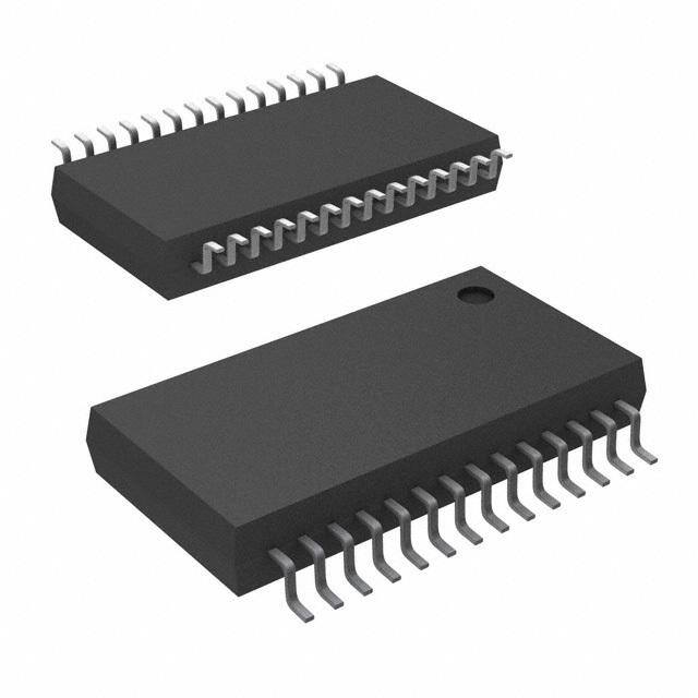
| 描述 | IC 10-BIT 40MHZ A/D 28-SSOP模数转换器 - ADC 10Bit 40MSPS SE/Diff Inp Int/Ext Ref |
| 产品分类 | |
| 品牌 | Texas Instruments |
| 产品手册 | http://www.ti.com/litv/sbas069b |
| 产品图片 |
|
| rohs | 符合RoHS无铅 / 符合限制有害物质指令(RoHS)规范要求 |
| 产品系列 | 数据转换器IC,模数转换器 - ADC,Texas Instruments ADS822E- |
| 数据手册 | |
| 产品型号 | ADS822E |
| PCN其它 | |
| 产品培训模块 | http://www.digikey.cn/PTM/IndividualPTM.page?site=cn&lang=zhs&ptm=13240 |
| 产品目录页面 | |
| 产品种类 | 模数转换器 - ADC |
| 位数 | 10 |
| 供应商器件封装 | 28-SSOP |
| 信噪比 | 60 dB |
| 分辨率 | 10 bit |
| 制造商产品页 | http://www.ti.com/general/docs/suppproductinfo.tsp?distId=10&orderablePartNumber=ADS822E |
| 包装 | 管件 |
| 单位重量 | 241.800 mg |
| 商标 | Texas Instruments |
| 安装类型 | 表面贴装 |
| 安装风格 | SMD/SMT |
| 封装 | Tube |
| 封装/外壳 | 28-SSOP(0.209",5.30mm 宽) |
| 封装/箱体 | SSOP-28 |
| 工作温度 | -40°C ~ 85°C |
| 工作电源电压 | 4.75 V to 5.25 V |
| 工厂包装数量 | 50 |
| 接口类型 | Parallel |
| 数据接口 | 并联 |
| 最大功率耗散 | 230 mW |
| 最大工作温度 | + 85 C |
| 最小工作温度 | - 40 C |
| 标准包装 | 50 |
| 电压参考 | Internal, External |
| 电压源 | 单电源 |
| 系列 | ADS822 |
| 结构 | Pipeline |
| 转换器数 | 1 |
| 转换器数量 | 1 |
| 转换速率 | 40000 kS/s |
| 输入数和类型 | 2 个单端,单极1 个差分,单极 |
| 输入类型 | Single-Ended/Differential |
| 通道数量 | 1 Channel |
| 采样率(每秒) | 40M |


- 商务部:美国ITC正式对集成电路等产品启动337调查
- 曝三星4nm工艺存在良率问题 高通将骁龙8 Gen1或转产台积电
- 太阳诱电将投资9.5亿元在常州建新厂生产MLCC 预计2023年完工
- 英特尔发布欧洲新工厂建设计划 深化IDM 2.0 战略
- 台积电先进制程称霸业界 有大客户加持明年业绩稳了
- 达到5530亿美元!SIA预计今年全球半导体销售额将创下新高
- 英特尔拟将自动驾驶子公司Mobileye上市 估值或超500亿美元
- 三星加码芯片和SET,合并消费电子和移动部门,撤换高东真等 CEO
- 三星电子宣布重大人事变动 还合并消费电子和移动部门
- 海关总署:前11个月进口集成电路产品价值2.52万亿元 增长14.8%


PDF Datasheet 数据手册内容提取
ADS822 ADS825 ADS825 ADS822 SBAS069B – MARCH 2001 – REVISED AUGUST 2002 10-Bit, 40MHz Sampling ANALOG-TO-DIGITAL CONVERTERS FEATURES (cid:1) +3V OR +5V LOGIC I/O COMPATIBLE (ADS825) (cid:1) POWER DOWN: 20mW (cid:1) HIGH SNR: 60dB (cid:1) SSOP-28 PACKAGE (cid:1) HIGH SFDR: 72dBFS (cid:1) LOW POWER: 190mW APPLICATIONS (cid:1) INTERNAL/EXTERNAL REFERENCE OPTION (cid:1) SINGLE-ENDED OR (cid:1) MEDICAL IMAGING FULLY DIFFERENTIAL ANALOG INPUT (cid:1) TEST EQUIPMENT (cid:1) PROGRAMMABLE INPUT RANGE (cid:1) COMPUTER SCANNERS (cid:1) LOW DNL: 0.5LSB (cid:1) COMMUNICATIONS (cid:1) SINGLE +5V SUPPLY OPERATION (cid:1) VIDEO DIGITIZING DESCRIPTION The ADS822 and ADS825 employ digital error correction techniques to provide excellent differential linearity for demanding imaging appli- The ADS822 and ADS825 are pipeline, CMOS Analog-to-Digital cations. Its low distortion and high SNR give the extra margin needed Converters (ADC) that operate from a single +5V power supply. for medical imaging, communications, video, and test instrumentation. These converters provide excellent performance with a single-ended The ADS822 and ADS825 offer power dissipation of 190mW and also input and can be operated with a differential input for added spurious provide a power-down mode, thus reducing power dissipation to only performance. These high-performance converters include a 10-bit 20mW. The ADS825 is +3V or +5V logic I/O compatible. quantizer, high-bandwidth track-and-hold, and a high-accuracy inter- The ADS822 and ADS825 are specified at a maximum sampling nal reference. They also allow for the user to disable the internal frequency of 40MSPS and a single-ended input range of 1.5V to 3.5V. reference and utilize external references. This external reference The ADS822 and ADS825 are available in an SSOP-28 package and option provides excellent gain and offset matching when used in are pin-for-pin compatible with the 10-bit, 60MSPS ADS823 and multichannel applications, or in applications where full-scale range ADS826, and the 10-bit, 75MSPS ADS828, providing an upgrade adjustment is required. path to higher sampling frequencies. +VS CLK VDRV ADS822 ADS825 Timing Circuitry VIN IN IN T/H PAi/1pD0e -ClBinoietred CoLErrorergcoitcrion O3-uStptauttes DD•••09 CM Internal Reference Int/Ext PD OE Optional External Reference Please be aware that an important notice concerning availability, standard warranty, and use in critical applications of Texas Instruments semiconductor products and disclaimers thereto appears at the end of this data sheet. PRODUCTION DATA information is current as of publication date. Copyright © 2001, Texas Instruments Incorporated Products conform to specifications per the terms of Texas Instruments standard warranty. Production processing does not necessarily include testing of all parameters. www.ti.com
ABSOLUTE MAXIMUM RATINGS(1) ELECTROSTATIC +V .......................................................................................................+6V DISCHARGE SENSITIVITY S Analog Input.............................................................–0.3V to (+V + 0.3V) S Logic Input...............................................................–0.3V to (+V + 0.3V) Case Temperature.........................................................................S +100°C This integrated circuit can be damaged by ESD. Texas Instru- Junction Temperature....................................................................+150°C ments recommends that all integrated circuits be handled with Storage Temperature.....................................................................+150°C appropriate precautions. Failure to observe proper handling NOTE: (1) Stresses above those listed under “Absolute Maximum Ratings” and installation procedures can cause damage. may cause permanent damage to the device. Exposure to absolute maximum conditions for extended periods may affect device reliability. ESD damage can range from subtle performance degradation to complete device failure. Precision integrated circuits may be DEMO BOARD ORDERING INFORMATION more susceptible to damage because very small parametric changes could cause the device not to meet its published PRODUCT DEMO BOARD specifications. ADS822E DEM-ADS822E PACKAGE/ORDERING INFORMATION SPECIFIED PACKAGE TEMPERATURE PACKAGE ORDERING TRANSPORT PRODUCT PACKAGE-LEAD DESIGNATOR(1) RANGE MARKING NUMBER MEDIA, QUANTITY ADS822 SSOP-28 DB –40°C to +85°C ADS822E ADS822E Rails, " " " " " ADS822E/1K Tape and Reel, 1000 ADS825 SSOP-28 DB –40°C to +85°C ADS825E ADS825E Rails, " " " " " ADS825E/1K Tape and Reel, 1000 NOTES: (1) For the most current specifications and package information, refer to our web site at www.ti.com. ELECTRICAL CHARACTERISTICS At T = full specified temperature range, V = +5V, single-ended input range = 1.5V to 3.5V, sampling rate = 40MHz and, external reference, unless otherwise noted. A S ADS822E ADS825E(1) PARAMETER CONDITIONS MIN TYP MAX MIN TYP MAX UNITS RESOLUTION 10 10 Bits SPECIFIED TEMPERATURE RANGE Ambient Air –40 to +85 –40 to +85 °C ANALOG INPUT Standard Single-Ended Input Range 2Vp-p 1.5 3.5 ✻ ✻ V Optional Single-Ended Input Range 1Vp-p 2 3 ✻ ✻ V Common-Mode Range 2.5 ✻ V Optional Differential Input Range 2Vp-p 2 3 ✻ ✻ V Analog Input Bias Current 1 ✻ µA Input Impedance 1.25 || 5 ✻ MΩ || pF Track-Mode Input Bandwidth –3dBFS Input 300 ✻ MHz CONVERSION CHARACTERISTICS Sample Rate 10k 40M ✻ ✻ Samples/s Data Latency 5 ✻ Clk Cyc DYNAMIC CHARACTERISTICS Differential Linearity Error (largest code error) f = 1MHz ±0.25 ±1.0 ✻ ✻ LSB f = 10MHz ±0.5 ✻ LSB No Missing Codes Tested Tested Integral Nonlinearity Error, f = 1MHz ±0.5 ±2.0 ✻ ✻ LSBs Spurious-Free Dynamic Range(2) Referred to Full-Scale f = 1MHz 72 71 dBFS(3) f = 10MHz 63 66 60 65 dBFS 2-Tone Intermodulation Distortion(4) f = 9.5MHz and 9.9MHz (–7dB each tone) –67 ✻ dBc Signal-to-Noise Ratio (SNR) Referred to Full-Scale f = 1MHz 60 ✻ dB f = 10MHz 57 60 ✻ ✻ dB Signal-to-(Noise + Distortion) (SINAD) Referred to Full-Scale f = 1MHz 59 ✻ dB f = 10MHz 56 58 ✻ ✻ dB Effective Number of Bits(5), f = 1MHz 9.5 ✻ Bits Output Noise Input Tied to Common-Mode 0.2 ✻ LSBs rms Aperture Delay Time 3 ✻ ns Aperture Jitter 1.2 ✻ ps rms Overvoltage Recovery Time 2 ✻ ns Full-Scale Step Acquisition Time 5 ✻ ns ADS822, ADS825 2 SBAS069B
ELECTRICAL CHARACTERISTICS (Cont.) At T = full specified temperature range, V = +5V, single-ended input range = 1.5V to 3.5V, and sampling rate = 40MHz, external reference, unless otherwise noted. A S ADS822E ADS825E(1) PARAMETER CONDITIONS MIN TYP MAX MIN TYP MAX UNITS DIGITAL INPUTS Logic Family CMOS-Compatible TTL, +3V/+5V CMOS-Compatible Convert Command Start Conversion Rising Edge of Convert Clock Rising Edge of Convert Clock High-Level Input Current(6) (V = 5V ) 100 ✻ µA IN DD Low-Level Input Current (V = 0V) 10 ✻ µA IN High-Level Input Voltage +3.5 +2.0 V Low-Level Input Voltage +1.0 +0.8 V Input Capacitance 5 ✻ pF DIGITAL OUTPUTS Logic Family CMOS-Compatible CMOS-Compatible Logic Coding Straight Offset Binary Straight Offset Binary Low Output Voltage (I = 50µA to 1.6mA) VDRV = 5V +0.1 ✻ V OL High Output Voltage, (I = 50µA to 0.5mA) +4.9 ✻ V OH Low Output Voltage, (I = 50µA to 1.6mA) VDRV = 3V +0.1 ✻ V OL High Output Voltage, (I = 50µA to 0.5mA) +2.8 ✻ V OH 3-State Enable Time OE = H to L 2 40 ✻ ✻ ns 3-State Disable Time OE = L to H 2 10 ✻ ✻ ns Output Capacitance 5 ✻ pF ACCURACY (Internal Reference, 2Vp-p, Unless Otherwise Noted) f = 2.5MHz S Zero Error (referred to –FS) at 25°C ±1.0 ±3.0 ✻ ✻ % FS Zero Error Drift (referred to –FS) 5 ✻ ppm/°C Midscale Offset Error at 25°C ±0.29 % FS Gain Error(7) at 25°C ±1.5 ±3.5 ✻ ✻ % FS Gain Error Drift(7) 38 ✻ ppm/°C Gain Error(8) at 25°C ±0.75 ±2.5 ✻ ✻ % FS Gain Error Drift(8) 25 ✻ ppm/°C Power-Supply Rejection of Gain ∆ V = ±5% 70 ✻ dB S REFT Tolerance Deviation From Ideal 3.5V ±10 ±25 ✻ ✻ mV REFB Tolerance(9) Deviation From Ideal 1.5V ±10 ±25 ✻ ✻ mV External REFT Voltage Range REFB + 0.8 3.5 V – 1.25 ✻ ✻ ✻ V S External REFB Voltage Range 1.25 1.5 REFT – 0.8 ✻ ✻ ✻ V Reference Input Resistance REFT to REFB 1.6 ✻ kΩ POWER-SUPPLY REQUIREMENTS Supply Voltage: +V Operating +4.75 +5.0 +5.25 ✻ ✻ ✻ V S Supply Current: +I Operating (External Reference) 40 ✻ mA S Power Dissipation: VDRV = 5V External Reference 200 230 ✻ ✻ mW VDRV = 3V External Reference 190 ✻ mW VDRV = 5V Internal Reference 250 ✻ mW VDRV = 3V Internal Reference 240 ✻ mW Power Down Operating 20 ✻ mW Thermal Resistance, θ JA SSOP-28 89 ✻ °C/W ✻ Indicates the same specifications as the ADS822E. NOTES: (1) ADS825E accepts a +3V clock input. (2) Spurious-Free Dynamic Range refers to the magnitude of the largest harmonic. (3) dBFS means dB relative to Full Scale. (4) Two-tone intermodulation distortion is referred to the largest fundamental tone. This number will be 6dB higher if it is referred to the magnitude of the two-tone fundamental envelope. (5) Effective number of bits (ENOB) is defined by (SINAD – 1.76)/6.02. (6) A 50kΩ pull-down resistor is inserted internally on OE pin. (7) Includes internal reference. (8) Excludes internal reference. (9) Assured by design. ADS822, ADS825 3 SBAS069B
PIN CONFIGURATION PIN DESCRIPTIONS Top View SSOP PIN DESIGNATOR DESCRIPTION 1 GND Ground 2 Bit 1 Data Bit 1 (D9) (MSB) 3 Bit 2 Data Bit 2 (D8) 4 Bit 3 Data Bit 3 (D7) 5 Bit 4 Data Bit 4 (D6) GND 1 28 VDRV 6 Bit 5 Data Bit 5 (D5) Bit 1 (MSB) 2 27 +V 7 Bit 6 Data Bit 6 (D4) S 8 Bit 7 Data Bit 7 (D3) Bit 2 3 26 GND 9 Bit 8 Data Bit 8 (D2) Bit 3 4 25 IN 10 Bit 9 Data Bit 9 (D1) 11 Bit 10 Data Bit 10 (D0) (LSB) Bit 4 5 24 IN 12 OE Output Enable. HI = high impedance state LO = normal operation (internal pull-down Bit 5 6 23 CM resistor) 13 PD Power Down. HI = enable; LO = disable Bit 6 7 ADS822 22 REFT 14 CLK Convert Clock Input ADS825 Bit 7 8 21 ByT 15 +V +5V Supply S 16 GND Ground Bit 8 9 20 ByB 17 RSEL Input Range Select. HI = 2V; LO = 1V Bit 9 10 19 REFB 18 INT/EXT Reference Select. HI = external, LO = internal 19 REFB Bottom Reference Bit 10 (LSB) 11 18 INT/EXT 20 ByB Bottom Ladder Bypass 21 ByT Top Ladder Bypass OE 12 17 RSEL 22 REFT Top Reference PD 13 16 GND 23 CM Common-Mode Voltage Output 24 IN Complementary Input (–) CLK 14 15 +V S 25 IN Analog Input (+) 26 GND Analog Ground 27 +V +5V Supply S 28 VDRV Output Logic Driver Supply Voltage TIMING DIAGRAM N+1 N+2 N+4 Analog In N+3 N+7 N N+5 N+6 tD tCONV tL tH Clock 5 Clock Cycles t 2 Data Out N–5 N–4 N–3 N–2 N–1 N N+1 N+2 Data Invalid t 1 SYMBOL DESCRIPTION MIN TYP MAX UNITS t Convert Clock Period 25 100µs ns CONV t Clock Pulse Low 11.5 12.5 ns L t Clock Pulse High 11.5 12.5 ns H t Aperture Delay 3 ns D t Data Hold Time, C = 0pF 3.9 ns 1 L t New Data Delay Time, C = 15pF max 12 ns 2 L ADS822, ADS825 4 SBAS069B
ELECTRICAL CHARACTERISTICS At T = full specified temperature range, V = +5V, single-ended input range = 1.5V to 3.5V, sampling rate = 40MHz, and external reference, unless otherwise noted. A S SPECTRAL PERFORMANCE SPECTRAL PERFORMANCE 0 0 f = 1MHz f = 10MHz IN IN –20 –20 B) B) e (d –40 e (d –40 d d u u nit nit g –60 g –60 a a M M –80 –80 –100 –100 0 5 10 15 20 0 5 10 15 20 Frequency (MHz) Frequency (MHz) SPECTRAL PERFORMANCE SPECTRAL PERFORMANCE (Differential Input, 1Vp-p) (Single-Ended, 1Vp-p) 0 0 f = 10MHz f = 10MHz IN IN SNR = 58dBFS SNR = 57dBFS –20 SFDR = 74dBFS –20 SFDR = 71dBFS B) B) e (d –40 e (d –40 d d u u nit nit g –60 g –60 a a M M –80 –80 –100 –100 0 5 10 15 20 0 5 10 15 20 Frequency (MHz) Frequency (MHz) SPECTRAL PERFORMANCE UNDERSAMPLING (Single-Ended, 1Vp-p) (Differential Input, 2Vp-p) 0 0 f = 20MHz f = 40MHz IN S SNR = 57dBFS f = 45MHz IN –20 SFDR = 70dBFS –20 SNR = 60dBFS SFDR = 74dBFS B) B) e (d –40 e (d –40 d d u u nit nit g –60 g –60 a a M M –80 –80 –100 –100 0 5 10 15 20 0 5 10 15 20 Frequency (MHz) Frequency (MHz) ADS822, ADS825 5 SBAS069B
ELECTRICAL CHARACTERISTICS (Cont.) At T = full specified temperature range, V = +5V, single-ended input range = 1.5V to 3.5V, sampling rate = 40MHz, and external reference, unless otherwise noted. A S UNDERSAMPLING (Differential Input, 2Vp-p) 2-TONE INTERMODULATION DISTORTION 0 0 f = 9.5MHz at –7dBFS f = 40MHz 1 S f = 9.9MHz at –7dBFS f = 75MHz 2 –20 SNINR = 59dBFS –20 IMD (3) = –67dB SFDR = 66dBFS B) B) e (d –40 e (d –40 d d u u nit nit g –60 g –60 a a M M –80 –80 –100 –100 0 5 10 15 20 0 5 10 15 20 Frequency (MHz) Frequency (MHz) DIFFERENTIAL LINEARITY ERROR DIFFERENTIAL LINEARITY ERROR 1.0 1.0 fIN = 1MHz fIN = 10MHz 0.5 0.5 B) B) S S E (L 0 E (L 0 DL DL –0.5 –0.5 –1.0 –1.0 0 128 256 512 768 1024 0 128 256 512 768 1024 Output Code Output Code INTEGRAL LINEARITY ERROR SWEPT POWER SFDR 2.0 100 80 1.0 c) B d dBFS ILE (LSB) 0 DR (dBFS, 6400 F –1.0 S dBc 20 –2.0 0 0 256 512 768 1024 –60 –50 –40 –30 –20 –10 0 Output Code Input Amplitude (dBFS) ADS822, ADS825 6 SBAS069B
ELECTRICAL CHARACTERISTICS (Cont.) At T = full specified temperature range, V = +5V, single-ended input range = 1.5V to 3.5V, sampling rate = 40MHz, and external reference, unless otherwise noted. A S DYNAMIC PERFORMANCE vs INPUT FREQUENCY DYNAMIC PERFORMANCE vs TEMPERATURE 75 75 70 S) SFDR S) 70 SFDR (f = 10MHz) F F IN B B d 65 d R ( R ( N N 65 S S SFDR (f = 20MHz) DR, 60 DR, IN SNR (fIN = 10MHz) F F S SNR S 60 55 SNR (f = 20MHz) IN 50 55 0.1 1 10 100 –50 –25 0 25 50 75 100 Frequency (MHz) Temperature (°C) SIGNAL-TO-(NOISE + DISTORTION) DIFFERENTIAL LINEARITY ERROR vs TEMPERATURE vs TEMPERATURE 60 .60 f = 1MHz IN f = 20MHz IN d (dBFS) 59 fIN = 10MHz E (LSB) .50 fIN = 10MHz a L n D Si 58 .40 f = 20MHz IN 57 .30 –50 –25 0 25 50 75 100 –50 –25 0 25 50 75 100 Temperature (°C) Temperature (°C) POWER DISSIPATION vs TEMPERATURE OUTPUT NOISE (DC Input) 205 800k 600k 200 W) m s er ( ount400k w C o P 195 200k 190 0 –50 –25 0 25 50 75 100 N-2 N-1 N N+1 N+2 Temperature (°C) Code ADS822, ADS825 7 SBAS069B
APPLICATION INFORMATION The selection for the optimum interface configuration will depend on the individual application requirements and sys- THEORY OF OPERATION tem structure. For example, communications applications The ADS822 and ADS825 are high-speed CMOS ADCs often process a band of frequencies that do not include DC, which employ a pipelined converter architecture consisting of whereas in imaging applications, the previously restored DC nine internal stages. Each stage feeds its data into the digital level must be maintained correctly up to the ADC. Features error correction logic ensuring excellent differential linearity on the ADS822 and ADS825, such as the input range select and no missing codes at the 10-bit level. The output data (RSEL pin) or the option for an external reference, provide becomes valid on the rising clock edge (see Timing Dia- the needed flexibility to accommodate a wide range of gram). The pipeline architecture results in a data latency of applications. In any case, the ADS822 and ADS825 should 5 clock cycles. be configured such that the application objectives are met while observing the headroom requirements of the driving The analog inputs of the ADS822 and ADS825 are differen- amplifier in order to yield the best overall performance. tial track-and-hold, as shown in Figure 1. The differential topology, along with tightly matched capacitors, produce a high level of AC performance while sampling at very high rates. INPUT CONFIGURATIONS AC-Coupled, Single-Supply Interface See Figure 2 for the typical circuit for an AC-coupled analog Op Amp input configuration of the ADS822 and ADS825 while all Bias VCM components are powered from a single +5V supply. φ1 φ1 With the RSEL pin connected HI, the full-scale input range is C set to 2Vp-p. In this configuration, the top and bottom H references (REFT, REFB) provide an output voltage of +3.5V φ2 CI and +1.5V, respectively. Two resistors ( 2x 1.62kΩ) are used IN φ1 φ2 φ1 OUT to create a common-mode voltage (VCM) of approximately IN OUT +2.5V to bias the inputs of the driving amplifier A1. Using the φ1 OPA680 on a single +5V supply, its ideal common-mode C I point is at +2.5V which coincides with the recommended φ2 CH common-mode input level for the ADS822 and ADS825. This φ1 φ1 obviates the need of a coupling capacitor between the Input Clock (50%) amplifier and the converter. Even though the OPA680 has an Op Amp V CM AC gain of +2, the DC gain is only +1 due to the blocking Bias capacitor at resistor R . G Internal Non-overlapping Clock The addition of a small series resistor (R ) between the φ1 φ2 φ1 S output of the op amp and the input of the ADS822 and ADS825 will be beneficial in almost all interface configura- tions. This will decouple the op amp’s output from the capacitive load and avoid gain peaking, which can result in FIGURE 1. Simplified Circuit of Input Track-and-Hold with increased noise. For best spurious and distortion perfor- Timing Diagram. mance, the resistor value should be kept below 100Ω. Furthermore, the series resistor in combination with the 10pF The ADS822 and ADS825 allow their analog inputs to be capacitor establishes a passive low-pass filter limiting the driven either single-ended or differentially. The typical con- bandwidth for the wideband noise, thus helping improve the figuration for the ADS822 and ADS825 is the single-ended SNR performance. mode in which the input track-and-hold performs a single- AC-Coupled, Dual Supply Interface ended-to-differential conversion of the analog input signal. The circuit provided in Figure 3 illustrates typical connections Both inputs (IN, IN) require external biasing using a com- for the analog input in case the selected amplifier operates mon-mode voltage that is typically at the mid-supply level on dual supplies. This might be necessary to take full (+V /2). S advantage of very low distortion operational amplifiers, like The following application discussion focuses on the single- the OPA642. The advantage is that the driving amplifier can ended configuration. Typically, its implementation is easier to be operated with a ground-referenced bipolar signal swing. achieve and the rated specifications for the ADS822 and This will keep the distortion performance at its lowest, since ADS825 are characterized using the single-ended mode of the signal range stays within the linear region of the op amp operation. and sufficient headroom to the supply rails can be main- tained. By capacitively coupling the single-ended signal to DRIVING THE ANALOG INPUT the input of the ADS822 and ADS825, its common-mode requirements can easily be satisfied with two resistors con- The ADS822 and ADS825 achieve excellent AC performance nected between the top and bottom references. either in the single-ended or differential mode of operation. ADS822, ADS825 8 SBAS069B
1.62kΩ +5V VCM +2.5V 1.62kΩ +5V 0.1µF 50Ω R REFB REFT RSEL +VS S +1.5V +3.5V V 50Ω IN OPA690 IN 10pF +V IN ADS822 0V R ADS825 F –V 402Ω IN CM IN R 402GΩ 0.1µF INT/EXT GND 0.1µF FIGURE 2. AC-Coupled Input Configuration for a 2Vp-p Full-Scale Range and a Common-Mode Voltage, V , at +2.5V Derived CM From the Internal Top (REFT) and Bottom References (REFB). +5V 1.62kΩ +5V REFT RSEL +V R S V 24.9SΩ 0.1µF +3.5V IN OPA642 IN 100pF ADS822 –5V ADS825 R 402FΩ 1.62kΩ CM IN RG 0.1µF REFB 402Ω +1.5V INT/EXT GND FIGURE 3. AC-Coupling the Dual Supply Amplifier, OPA642, to the ADS822 for a 2Vp-p Full-Scale Input Range. For applications requiring the driving amplifier to provide a the +2.5V common-mode voltage available at the CM pin. signal amplification, with a gain ≥ 5, consider using decom- One half of amplifier A1 buffers the REFB pin and drives the pensated voltage-feedback op amps, like the OPA686, or voltage dividers R , R . Due to the op amp’s noise gain of 1 2 current-feedback op amps like the OPA691. +2V/V, assuming R = R , the common-mode voltage (V ) F IN CM DC-coupled with Level Shift has to be re-scaled to +1.25V. This results in the correct DC level of +2.5V for the signal input (IN). Any DC voltage Several applications may require that the bandwidth of the differences between the IN and IN inputs of the ADS822 and signal path include DC, in which case, the signal has to be ADS825 effectively produces an offset, which can be cor- DC-coupled to the ADC. In order to accomplish this, the rected for by adjusting the resistor values of the divider, R interface circuit has to provide a DC level shift to the analog 1 and R . The selection criteria for a suitable op amp should input signal. See Figure 4 for a circuit that employs a dual op 2 include the supply voltage, input bias current, output voltage amp, A1, to drive the input of the ADS822 and ADS825, and swing, distortion, and noise specification. Note that in this level shifts the signal to be compatible with the selected input example, the overall signal phase is inverted. To re-establish range. With the RSEL pin tied to the supply and the INT/EXT the original signal polarity, it is always possible to inter- pin to ground, the ADS822 and ADS825 are configured for a change the IN and IN connections. 2Vp-p input range and use the internal references. The complementary input (IN) may be appropriately biased using ADS822, ADS825 9 SBAS069B
+5V R F 499Ω R 499INΩ R RSEL +VS VIN 1/2 A1 50SΩ OPA2691 IN 2Vp-p 10pF ADS822 ADS825 NOTE: RF = RIN, G = –1 CM (+2.5) IN 0.1µF +5V REFB REFT (+1.5V) (+3.5V) INT/EXT R A2 50Ω 2002Ω 0.1µF 1/2 VCM = +1.25V OPA2691 0.1µF R 1 1kΩ R F 1kΩ FIGURE 4. DC-Coupled Interface Circuit with Dual Current-Feedback Amplifier OPA2681. SINGLE-ENDED-TO-DIFFERENTIAL CONFIGURATION The component values of the R-C low-pass may be opti- (Transformer Coupled) mized depending on the desired roll-off frequency. The If the application requires a signal conversion from a single- resistor across the secondary side (RT) should be calculated ended source to feed the ADS822 and ADS825 differentially, using the equation RT = n2 • RG to match the source impedance a RF transformer might be a good solution. The selected (RG) for good power transfer and Voltage Standing Wave Ratio transformer must have a center tap in order to apply the (VSWR). common-mode DC voltage necessary to bias the converter inputs. AC-grounding the center tap will generate the differ- REFERENCE OPERATION ential signal swing across the secondary winding. Consider Figure 6 depicts the simplified model of the internal reference a step-up transformer to take advantage of a signal amplifi- circuit. The internal blocks are the bandgap voltage refer- cation without the introduction of another noise source. ence, the drivers for the top and bottom references, and the Furthermore, the reduced signal swing from the source may lead to an improved distortion performance. The differential input configuration may provide a noticeable RSEL +VS INT/EXT advantage of achieving good SFDR performance over a wide range of input frequencies. In this mode, both inputs of the ADS822 50kΩ 50kΩ ADS822 and ADS825 see matched impedances, and the differential signal swing can be reduced to half of the swing Bandgap Reference and Logic required for single-ended drive. Figure 5 shows the sche- V REF matic for the suggested transformer-coupled interface circuit. RG +1 +1 0.1µF 1:n 22Ω V IN IN 47pF 400Ω 400Ω 400Ω 400Ω ADS822 R T ADS825 22Ω IN REFT ByT CM ByB REFB CM RSEL INT/EXT 47pF +5V + 10µF 0.1µF Bypass Capacitors: 0.1µF || 2.2µF each (optionally, 2.2µF tantalum capacitors maybe added to ByT and ByB pins for the best results). FIGURE 6. Equivalent Reference Circuit with Recommended FIGURE 5. Transformer Coupled Input. Reference Bypassing. ADS822, ADS825 10 SBAS069B
resistive reference ladder. The bandgap reference circuit The common-mode voltage available at the CM pin may be includes logic functions that allows setting the analog input used as a bias voltage to provide the appropriate offset for swing of the ADS822 and ADS825 to either a 1Vp-p or the driving circuitry. However, care must be taken not to 2Vp-p full-scale range simply by tying the RSEL pin to a Low appreciably load this node, which is not buffered and has a or High potential, respectively. While operating the ADS822 high impedance. An alternative way of generating a com- in the external reference mode, the buffer amplifiers for the mon-mode voltage is given in Figure 7. Here, two external REFT and REFB are disconnected from the reference lad- precision resistors (tolerance 1% or better) are located der. between the top and bottom reference pins. The common- As shown, the ADS822 and ADS825 have internal 50kΩ pull- mode voltage, CMV, will appear at the midpoint. up resistors at the range select pin (RSEL) and reference select pin (INT/EXT). Leaving these pins open configures the EXTERNAL REFERENCE OPERATION ADS822 and ADS825 for a 2Vp-p input range and external For even more design flexibility, the internal reference can be reference operation. Setting the ADS822 and ADS825 up for disabled and an external reference voltage be used. The internal reference mode requires bringing the INT/EXT pin utilization of an external reference may be considered for Low. applications requiring higher accuracy, improved tempera- The reference buffers can be utilized to supply up to 1mA ture performance, or a wide adjustment range of the (sink and source) to external circuitry. The resistor ladders of converter’s full-scale range. Especially in multichannel the ADS822 and ADS825 are divided into several segments applications, the use of a common external reference has the and have two additional nodes, ByT and ByB, which are benefit of obtaining better matching of the full-scale range brought out for external bypassing only (see Figure 6). To between converters. ensure proper operation with any reference configurations, it The external references can vary as long as the value of the is necessary to provide solid bypassing at all reference pins external top reference REFT stays within the range of in order to keep the clock feedthrough to a minimum. All EXT (V – 1.25V) and (REFB + 0.8V), and the external bottom bypassing capacitors should be located as close to their S reference REFB stays within 1.25V and (REFT – 0.8V) respective pins as possible. EXT (See Figure 8). DIGITAL INPUTS AND OUTPUTS ADS822 Clock Input Requirements REFT ADS825 REFB +3.5V +1.5V Clock jitter is critical to the SNR performance of high-speed, R1 R2 high-resolution ADCs. Clock jitter leads to aperture jitter (tA), 1.6kΩ 1.6kΩ which adds noise to the signal being converted. The ADS822 and ADS825 samples the input signal on the rising edge of the 0.1µF 0.1µF CLK input. Therefore, this edge should have the lowest pos- CMV +2.5V sible jitter. The jitter noise contribution to total SNR is given by FIGURE 7. Alternative Circuit to Generate CM Voltage. +5V A - Short for 1Vp-p Input Range B A B - Short for 2Vp-p Input Range (Default) +VS INT/EXT RSEL GND V IN IN ADS822 ADS825 CMV IN +2.5V DC REFT ByT GND ByB REFB External Top Reference External Bottom Reference REFT = REFB +0.8V to +3.75V 4 x 0.1µF REFB = REFT –0.8V to +1.25V FIGURE 8. Configuration Example for External Reference Operation. ADS822, ADS825 11 SBAS069B
the following equation. If this value is near your system Digital Output Driver (VDRV) requirements, input clock jitter must be reduced. The ADS822 features a dedicated supply pin for the output logic drivers, VDRV, which are not internally connected to 1 Jitter SNR=20log rms signal tormsnoise the other supply pins. Setting the voltage at VDRV to +5V or 2πƒ t IN A +3V, the ADS822 and ADS825 produce corresponding logic levels and can directly interface to the selected logic family. where: ƒ is input signal frequency IN The output stages are designed to supply sufficient current t is rms clock jitter A to drive a variety of logic families. However, it is recom- Particularly in undersampling applications, special consider- mended to use the ADS822 and ADS825 with +3V logic supply. This will lower the power dissipation in the output ation should be given to clock jitter. The clock input should be stages due to the lower output swing and reduce current treated as an analog input in order to achieve the highest glitches on the supply line which may affect the AC-perfor- level of performance. Any overshoot or undershoot of the mance of the converter. In some applications, it might be clock signal may cause degradation of the performance. advantageous to decouple the VDRV pin with additional When digitizing at high sampling rates, the clock should have capacitors or a pi filter. 50% duty cycle (t = t ), along with fast rise and fall times of H L 2ns or less. The clock input of the ADS825 can be driven with GROUNDING AND DECOUPLING either 3V or 5V logic levels. Using low-voltage logic (3V) may Proper grounding and bypassing, short lead length, and the lead to improved AC performance of the converter. use of ground planes are particularly important for high- Digital Outputs frequency designs. Multilayer PC boards are recommended The output data format of the ADS822 and ADS825 are in for best performance since they offer distinct advantages like positive Straight Offset Binary code, as shown in Tables I minimizing ground impedance, separation of signal layers by and II. This format can easily be converted into the Binary ground layers, etc. The ADS822 and ADS825 should be Two’s Complement code by inverting the MSB. treated as analog components. Whenever possible, the supply pins should be powered by the analog supply. This It is recommended to keep the capacitive loading on the data will ensure the most consistent results, since digital supply lines as low as possible (≤ 15pF). Higher capacitive loading lines often carry high levels of noise which otherwise would will cause larger dynamic currents as the digital outputs are be coupled into the converter and degrade the achievable changing. Those high current surges can feed back to the performance. All ground connections on the ADS822 and analog portion of the ADS822 and ADS825 and affect the ADS825 are internally joined together obviating the design of performance. If necessary, external buffers or latches close split ground planes. The ground pins (1, 16, 26) should to the converter’s output pins may be used to minimize the directly connect to an analog ground plane which covers the capacitive loading. They also provide the added benefit of PC board area around the converter. While designing the isolating the ADS822 and ADS825 from any digital noise layout, it is important to keep the analog signal traces activities on the bus coupling back high frequency noise. separated from any digital lines to prevent noise coupling onto the analog signal path. Due to their high sampling rates, the ADS822 and ADS825 generate high frequency current SINGLE-ENDED INPUT STRAIGHT OFFSET BINARY (IN = CMV) (SOB) transients, and noise (clock feedthrough) that are fed back into the supply and reference lines. This requires that all +FS –1LSB (IN = REFT) 11 1111 1111 supply and reference pins are sufficiently bypassed. +1/2 Full Scale 11 0000 0000 Figure 9 shows the recommended decoupling scheme for Bipolar Zero (IN = CMV) 10 0000 0000 –1/2 Full Scale 01 0000 0000 the ADS822 and ADS825. In most cases, 0.1µF ceramic –FS (IN = REFB) 00 0000 0000 chip capacitors at each pin are adequate to keep the imped- ance low over a wide frequency range. Their effectiveness TABLE I. Coding Table for Single-Ended Input Configuration largely depends on the proximity to the individual supply pin. with IN Tied to the Common-Mode Voltage (CMV). Therefore, they should be located as close to the supply pins as possible. In addition, a larger bipolar capacitor (1µF to 22µF) should be placed on the PC board in proximity of the STRAIGHT OFFSET BINARY converter circuit. DIFFERENTIAL INPUT (SOB) +FS –1LSB (IN = +3V, IN = +2V) 11 1111 1111 +1/2 Full Scale 11 0000 0000 ADS822 Bipolar Zero (IN = IN = CMV) 10 0000 0000 ADS825 –1/2 Full Scale 01 0000 0000 +V GND +V GND VDRV –FS (IN = +2V, IN = +3V) 00 0000 0000 S S 27 26 15 16 28 TABLE II. Coding Table for Differential Input Configuration and 0.1µF 0.1µF 0.1µF 2Vp-p Full-Scale Range. 10µF + +5V +3/+5V FIGURE 9. Recommended Bypassing for the Supply Pins. ADS822, ADS825 12 SBAS069B
PACKAGE OPTION ADDENDUM www.ti.com 6-Feb-2020 PACKAGING INFORMATION Orderable Device Status Package Type Package Pins Package Eco Plan Lead/Ball Finish MSL Peak Temp Op Temp (°C) Device Marking Samples (1) Drawing Qty (2) (6) (3) (4/5) ADS822E ACTIVE SSOP DB 28 50 Green (RoHS NIPDAU Level-2-260C-1 YEAR -40 to 85 ADS822E & no Sb/Br) ADS822E/1K ACTIVE SSOP DB 28 1000 Green (RoHS NIPDAU Level-2-260C-1 YEAR -40 to 85 ADS822E & no Sb/Br) ADS825E ACTIVE SSOP DB 28 50 Green (RoHS NIPDAU Level-2-260C-1 YEAR -40 to 85 ADS825E & no Sb/Br) ADS825E/1K ACTIVE SSOP DB 28 1000 Green (RoHS NIPDAU Level-2-260C-1 YEAR -40 to 85 ADS825E & no Sb/Br) (1) The marketing status values are defined as follows: ACTIVE: Product device recommended for new designs. LIFEBUY: TI has announced that the device will be discontinued, and a lifetime-buy period is in effect. NRND: Not recommended for new designs. Device is in production to support existing customers, but TI does not recommend using this part in a new design. PREVIEW: Device has been announced but is not in production. Samples may or may not be available. OBSOLETE: TI has discontinued the production of the device. (2) RoHS: TI defines "RoHS" to mean semiconductor products that are compliant with the current EU RoHS requirements for all 10 RoHS substances, including the requirement that RoHS substance do not exceed 0.1% by weight in homogeneous materials. Where designed to be soldered at high temperatures, "RoHS" products are suitable for use in specified lead-free processes. TI may reference these types of products as "Pb-Free". RoHS Exempt: TI defines "RoHS Exempt" to mean products that contain lead but are compliant with EU RoHS pursuant to a specific EU RoHS exemption. Green: TI defines "Green" to mean the content of Chlorine (Cl) and Bromine (Br) based flame retardants meet JS709B low halogen requirements of <=1000ppm threshold. Antimony trioxide based flame retardants must also meet the <=1000ppm threshold requirement. (3) MSL, Peak Temp. - The Moisture Sensitivity Level rating according to the JEDEC industry standard classifications, and peak solder temperature. (4) There may be additional marking, which relates to the logo, the lot trace code information, or the environmental category on the device. (5) Multiple Device Markings will be inside parentheses. Only one Device Marking contained in parentheses and separated by a "~" will appear on a device. If a line is indented then it is a continuation of the previous line and the two combined represent the entire Device Marking for that device. (6) Lead/Ball Finish - Orderable Devices may have multiple material finish options. Finish options are separated by a vertical ruled line. Lead/Ball Finish values may wrap to two lines if the finish value exceeds the maximum column width. Important Information and Disclaimer:The information provided on this page represents TI's knowledge and belief as of the date that it is provided. TI bases its knowledge and belief on information provided by third parties, and makes no representation or warranty as to the accuracy of such information. Efforts are underway to better integrate information from third parties. TI has taken and Addendum-Page 1
PACKAGE OPTION ADDENDUM www.ti.com 6-Feb-2020 continues to take reasonable steps to provide representative and accurate information but may not have conducted destructive testing or chemical analysis on incoming materials and chemicals. TI and TI suppliers consider certain information to be proprietary, and thus CAS numbers and other limited information may not be available for release. In no event shall TI's liability arising out of such information exceed the total purchase price of the TI part(s) at issue in this document sold by TI to Customer on an annual basis. Addendum-Page 2
PACKAGE MATERIALS INFORMATION www.ti.com 26-Feb-2019 TAPE AND REEL INFORMATION *Alldimensionsarenominal Device Package Package Pins SPQ Reel Reel A0 B0 K0 P1 W Pin1 Type Drawing Diameter Width (mm) (mm) (mm) (mm) (mm) Quadrant (mm) W1(mm) ADS822E/1K SSOP DB 28 1000 330.0 16.4 8.1 10.4 2.5 12.0 16.0 Q1 ADS825E/1K SSOP DB 28 1000 330.0 16.4 8.1 10.4 2.5 12.0 16.0 Q1 PackMaterials-Page1
PACKAGE MATERIALS INFORMATION www.ti.com 26-Feb-2019 *Alldimensionsarenominal Device PackageType PackageDrawing Pins SPQ Length(mm) Width(mm) Height(mm) ADS822E/1K SSOP DB 28 1000 350.0 350.0 43.0 ADS825E/1K SSOP DB 28 1000 367.0 367.0 38.0 PackMaterials-Page2
PACKAGE OUTLINE DB0028A SSOP - 2 mm max height SCALE 1.500 SMALL OUTLINE PACKAGE C 8.2 TYP 7.4 A 0.1 C PIN 1 INDEX AREA SEATING PLANE 26X 0.65 28 1 2X 10.5 8.45 9.9 NOTE 3 14 15 0.38 28X 0.22 5.6 0.15 C A B B 5.0 NOTE 4 2 MAX 0.25 (0.15) TYP SEE DETAIL A GAGE PLANE 0 -8 0.95 0.05 MIN 0.55 DETA 15AIL A TYPICAL 4214853/B 03/2018 NOTES: 1. All linear dimensions are in millimeters. Any dimensions in parenthesis are for reference only. Dimensioning and tolerancing per ASME Y14.5M. 2. This drawing is subject to change without notice. 3. This dimension does not include mold flash, protrusions, or gate burrs. Mold flash, protrusions, or gate burrs shall not exceed 0.15 mm per side. 4. This dimension does not include interlead flash. Interlead flash shall not exceed 0.25 mm per side. 5. Reference JEDEC registration MO-150. www.ti.com
EXAMPLE BOARD LAYOUT DB0028A SSOP - 2 mm max height SMALL OUTLINE PACKAGE 28X (1.85) SYMM (R0.05) TYP 1 28X (0.45) 28 26X (0.65) SYMM 14 15 (7) LAND PATTERN EXAMPLE EXPOSED METAL SHOWN SCALE: 10X SOLDER MASK METAL METAL UNDER SOLDER MASK OPENING SOLDER MASK OPENING EXPOSED METAL EXPOSED METAL 0.07 MAX 0.07 MIN ALL AROUND ALL AROUND NON-SOLDER MASK SOLDER MASK DEFINED DEFINED (PREFERRED) SOLDE15.000 R MASK DETAILS 4214853/B 03/2018 NOTES: (continued) 6. Publication IPC-7351 may have alternate designs. 7. Solder mask tolerances between and around signal pads can vary based on board fabrication site. www.ti.com
EXAMPLE STENCIL DESIGN DB0028A SSOP - 2 mm max height SMALL OUTLINE PACKAGE 28X (1.85) SYMM (R0.05) TYP 1 28X (0.45) 28 26X (0.65) SYMM 14 15 (7) SOLDER PASTE EXAMPLE BASED ON 0.125 mm THICK STENCIL SCALE: 10X 4214853/B 03/2018 NOTES: (continued) 8. Laser cutting apertures with trapezoidal walls and rounded corners may offer better paste release. IPC-7525 may have alternate design recommendations. 9. Board assembly site may have different recommendations for stencil design. www.ti.com
IMPORTANTNOTICEANDDISCLAIMER TI PROVIDES TECHNICAL AND RELIABILITY DATA (INCLUDING DATASHEETS), DESIGN RESOURCES (INCLUDING REFERENCE DESIGNS), APPLICATION OR OTHER DESIGN ADVICE, WEB TOOLS, SAFETY INFORMATION, AND OTHER RESOURCES “AS IS” AND WITH ALL FAULTS, AND DISCLAIMS ALL WARRANTIES, EXPRESS AND IMPLIED, INCLUDING WITHOUT LIMITATION ANY IMPLIED WARRANTIES OF MERCHANTABILITY, FITNESS FOR A PARTICULAR PURPOSE OR NON-INFRINGEMENT OF THIRD PARTY INTELLECTUAL PROPERTY RIGHTS. These resources are intended for skilled developers designing with TI products. You are solely responsible for (1) selecting the appropriate TI products for your application, (2) designing, validating and testing your application, and (3) ensuring your application meets applicable standards, and any other safety, security, or other requirements. These resources are subject to change without notice. TI grants you permission to use these resources only for development of an application that uses the TI products described in the resource. Other reproduction and display of these resources is prohibited. No license is granted to any other TI intellectual property right or to any third party intellectual property right. TI disclaims responsibility for, and you will fully indemnify TI and its representatives against, any claims, damages, costs, losses, and liabilities arising out of your use of these resources. TI’s products are provided subject to TI’s Terms of Sale (www.ti.com/legal/termsofsale.html) or other applicable terms available either on ti.com or provided in conjunction with such TI products. TI’s provision of these resources does not expand or otherwise alter TI’s applicable warranties or warranty disclaimers for TI products. Mailing Address: Texas Instruments, Post Office Box 655303, Dallas, Texas 75265 Copyright © 2020, Texas Instruments Incorporated