ICGOO在线商城 > 集成电路(IC) > 数据采集 - 模数转换器 > ADS803E
 Datasheet下载
- 型号: ADS803E
- 制造商: Texas Instruments
- 库位|库存: xxxx|xxxx
- 要求:
| 数量阶梯 | 香港交货 | 国内含税 |
| +xxxx | $xxxx | ¥xxxx |
查看当月历史价格
查看今年历史价格
ADS803E产品简介:
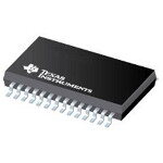
ICGOO电子元器件商城为您提供ADS803E由Texas Instruments设计生产,在icgoo商城现货销售,并且可以通过原厂、代理商等渠道进行代购。 ADS803E价格参考¥105.70-¥176.27。Texas InstrumentsADS803E封装/规格:数据采集 - 模数转换器, 12 Bit Analog to Digital Converter 1 Input 1 Pipelined 28-SSOP。您可以下载ADS803E参考资料、Datasheet数据手册功能说明书,资料中有ADS803E 详细功能的应用电路图电压和使用方法及教程。
Texas Instruments(德州仪器)的ADS803E是一款高性能、低功耗的12位模数转换器(ADC),属于数据采集系统中的关键组件。以下是ADS803E的主要应用场景:

 1. 工业自动化与控制
   - ADS803E适用于工业自动化设备中的数据采集模块,例如传感器信号的数字化处理。
   - 可用于温度、压力、流量等模拟信号的高精度采集,支持实时监控和反馈控制。

 2. 医疗设备
   - 在医疗领域,ADS803E可用于心电图(ECG)、脑电图(EEG)等设备中,实现生物电信号的精确转换。
   - 其低功耗特性有助于延长便携式医疗设备的电池寿命。

 3. 通信系统
   - ADS803E适合用作通信基站或无线设备中的信号调理模块,完成射频信号的数字化处理。
   - 高速采样能力使其能够满足现代通信系统的带宽需求。

 4. 消费电子
   - 在音频设备中,ADS803E可将模拟音频信号转换为数字信号,用于后续处理或存储。
   - 适用于家用音响、麦克风阵列等需要高质量音频采集的应用。

 5. 汽车电子
   - ADS803E可用于汽车传感器的数据采集,如胎压监测、发动机状态监控等。
   - 其可靠性和稳定性满足车载环境对电子元件的严格要求。

 6. 测试与测量
   - 在示波器、信号发生器等测试设备中,ADS803E负责将输入的模拟信号转换为数字信号,以便进行分析和显示。
   - 提供高分辨率和快速响应,确保测量结果的准确性。

 7. 能源管理
   - ADS803E可用于电力监控系统中,采集电压、电流等参数,实现智能电网的高效管理。
   - 在太阳能逆变器等新能源设备中,用于优化能量转换效率。

ADS803E凭借其出色的性能指标(如12位分辨率、低功耗设计和高线性度),成为多种应用领域的理想选择。其紧凑的封装形式也便于集成到各种复杂系统中。
| 参数 | 数值 |
| 产品目录 | 集成电路 (IC)半导体 |
| 描述 | IC 12-BIT 5MHZ A/D 28-SSOP模数转换器 - ADC 12-Bit 5 MSPS Int/Ext Ref |
| 产品分类 | |
| 品牌 | Texas Instruments |
| 产品手册 | |
| 产品图片 |
|
| rohs | 符合RoHS无铅 / 符合限制有害物质指令(RoHS)规范要求 |
| 产品系列 | 数据转换器IC,模数转换器 - ADC,Texas Instruments ADS803E- |
| 数据手册 | |
| 产品型号 | ADS803E |
| PCN其它 | |
| 产品培训模块 | http://www.digikey.cn/PTM/IndividualPTM.page?site=cn&lang=zhs&ptm=13240 |
| 产品目录页面 | |
| 产品种类 | 模数转换器 - ADC |
| 位数 | 12 |
| 供应商器件封装 | 28-SSOP |
| 信噪比 | 69 dB |
| 分辨率 | 12 bit |
| 制造商产品页 | http://www.ti.com/general/docs/suppproductinfo.tsp?distId=10&orderablePartNumber=ADS803E |
| 包装 | 管件 |
| 单位重量 | 241.800 mg |
| 商标 | Texas Instruments |
| 安装类型 | 表面贴装 |
| 安装风格 | SMD/SMT |
| 封装 | Tube |
| 封装/外壳 | 28-SSOP(0.209",5.30mm 宽) |
| 封装/箱体 | SSOP-28 |
| 工作温度 | -40°C ~ 85°C |
| 工作电源电压 | 4.75 V to 5.25 V |
| 工厂包装数量 | 50 |
| 接口类型 | Parallel |
| 数据接口 | 并联 |
| 最大功率耗散 | 135 mW |
| 最大工作温度 | + 85 C |
| 最小工作温度 | - 40 C |
| 标准包装 | 50 |
| 特性 | - |
| 电压参考 | Internal, External |
| 电压源 | 单电源 |
| 系列 | ADS803 |
| 结构 | Pipeline |
| 转换器数 | 1 |
| 转换器数量 | 1 |
| 转换速率 | 5000 kS/s |
| 输入数和类型 | 2 个单端,单极1 个差分,单极 |
| 输入类型 | Single-Ended/Differential |
| 通道数量 | 1 Channel |
| 采样率(每秒) | 5M |


- 商务部:美国ITC正式对集成电路等产品启动337调查
- 曝三星4nm工艺存在良率问题 高通将骁龙8 Gen1或转产台积电
- 太阳诱电将投资9.5亿元在常州建新厂生产MLCC 预计2023年完工
- 英特尔发布欧洲新工厂建设计划 深化IDM 2.0 战略
- 台积电先进制程称霸业界 有大客户加持明年业绩稳了
- 达到5530亿美元!SIA预计今年全球半导体销售额将创下新高
- 英特尔拟将自动驾驶子公司Mobileye上市 估值或超500亿美元
- 三星加码芯片和SET,合并消费电子和移动部门,撤换高东真等 CEO
- 三星电子宣布重大人事变动 还合并消费电子和移动部门
- 海关总署:前11个月进口集成电路产品价值2.52万亿元 增长14.8%


PDF Datasheet 数据手册内容提取
ADS803 ADS803E SBAS074B – JANUARY 1997 – REVISED SEPTEMBER 2002 12-Bit, 5MHz Sampling ANALOG-TO-DIGITAL CONVERTER FEATURES APPLICATIONS (cid:1) HIGH SFDR: 82dB at NYQUIST (cid:1) IF AND BASEBAND DIGITIZATION (cid:1) HIGH SNR: 69dB (cid:1) CCD IMAGING SCANNERS (cid:1) LOW POWER: 115mW (cid:1) TEST INSTRUMENTATION (cid:1) LOW DLE: 0.25LSB (cid:1) FLEXIBLE INPUT RANGE (cid:1) OVER-RANGE INDICATOR DESCRIPTION 0.09LSBs rms giving superior imaging performance. There is also a capability to set the input range in between the 2Vp-p The ADS803 is a high-speed, high dynamic range, 12-bit and 5Vp-p input ranges or to use an external reference. The pipelined Analog-to-Digital (A/D) converter. This converter ADS803 also provides an over-range indicator flag to indicate includes a high-bandwidth track-and-hold that gives excel- an input range that exceeds the full-scale input range of the lent spurious performance up to and beyond the Nyquist rate. converter. This flag can be used to reduce the gain of the front- This high-bandwidth, linear track-and-hold minimizes har- end gain-ranging circuitry. monics and has low jitter, leading to excellent SNR perfor- The ADS803 employs digital error-correction techniques to mance. The ADS803 is also pin-compatible with the 10MHz provide excellent differential linearity for demanding imaging ADS804 and the 20MHz ADS805. applications. Its low distortion and high SNR give the extra The ADS803 provides an internal reference and can be margin needed for communications, medical imaging, video, programmed for a 2Vp-p input range for the best spurious and test instrumentation applications. The ADS803 is avail- performance and ease of driving. Alternatively, the 5Vp-p input able in an SSOP-28 package. range can be used for the lowest input referred noise of +V CLK VDRV S ADS803 Timing Circuitry VIN IN 12-Bit Error D0 3-State • IN T & H Pipelined Correction Outputs •• ADC Logic D11 CM Reference Ladder OVR and Driver Reference and Mode Select REFT V SEL REFB OE REF Please be aware that an important notice concerning availability, standard warranty, and use in critical applications of Texas Instruments semiconductor products and disclaimers thereto appears at the end of this data sheet. PRODUCTION DATA information is current as of publication date. Copyright © 1997, Texas Instruments Incorporated Products conform to specifications per the terms of Texas Instruments standard warranty. Production processing does not necessarily include testing of all parameters. www.ti.com
ABSOLUTE MAXIMUM RATINGS(1) ELECTROSTATIC +VS.......................................................................................................+6V DISCHARGE SENSITIVITY Analog Input...........................................................(–0.3V) to (+V +0.3V) S Logic Input.............................................................(–0.3V) to (+V +0.3V) S This integrated circuit can be damaged by ESD. Texas Instru- Case Temperature.........................................................................+100°C Junction Temperature....................................................................+150°C ments recommends that all integrated circuits be handled with Storage Temperature.....................................................................+150°C appropriate precautions. Failure to observe proper handling and installation procedures can cause damage. NOTE: (1) Stresses above those listed under “Absolute Maximum Ratings” may cause permanent damage to the device. Exposure to absolute maximum ESD damage can range from subtle performance degrada- conditions for extended periods may affect device reliability. tion to complete device failure. Precision integrated circuits may be more susceptible to damage because very small parametric changes could cause the device not to meet its published specifications. PACKAGE/ORDERING INFORMATION SPECIFIED PACKAGE TEMPERATURE PACKAGE ORDERING TRANSPORT PRODUCT PACKAGE-LEAD DESIGNATOR(1) RANGE MARKING NUMBER MEDIA, QUANTITY ADS803E SSOP-28 DB –40°C to +85°C ADS803E ADS803E Rails, 48 " " " " " ADS803E/1K Tape and Reel, 1000 NOTE: (1) For the most current specifications and package information, refer to our web site at www.ti.com. ELECTRICAL CHARACTERISTICS At T = full specified temperature range, V = +5V, specified input range = 1.5V to 3.5V, single-ended input and sampling rate = 5MHz, unless otherwise specified. A S ADS803E PARAMETER CONDITIONS MIN TYP MAX UNITS RESOLUTION 12 Tested Bits SPECIFIED TEMPERATURE RANGE –40 +85 °C CONVERSION CHARACTERISTICS Sample Rate 10k 5M Samples/s Data Latency 6 Clk Cycles ANALOG INPUT Single-Ended Input Range 1.5 3.5 V Standard Optional Single-Ended Input Range 0 5 V Common-Mode Voltage 2.5 V Standard Optional Common-Mode Voltage 1 V Input Capacitance 20 pF Track-Mode Input Bandwidth –3dBFS Input 270 MHz DYNAMIC CHARACTERISTICS Differential Linearity Error (Largest Code Error) f = 500kHz ±0.25 ±0.75 LSB No Missing Codes Tested Spurious-Free Dynamic Range(1) f = 2.48MHz (–1dB input) 74 82 dBFS(2) 2-Tone Intermodulation Distortion(3) 74 dBc f = 1.8M and 1.9M (–7dBFS each tone) Signal-to-Noise Ratio (SNR) f = 2.48MHz (–1dB input) 66.5 69 dB Signal-to-(Noise + Distortion) (SINAD) f = 2.48MHz (–1dB input) 65 68 dB Effective Number of Bits at 2.48MHz(4) 11 Bits Input Referred Noise 0V to 5V Input 0.09 LSBs rms 1.5V to 3.5V Input 0.23 LSBs rms Integral Nonlinearity Error f = 500kHz ±1 ±2 LSB Aperture Delay Time 1 ns Aperture Jitter 4 ps rms Over-Voltage Recovery Time 1.5 • FS Input 2 ns Full-Scale Step Acquisition Time 50 ns ADS803 2 www.ti.com SBAS074B
ELECTRICAL CHARACTERISTICS (Cont.) At T = full specified temperature range, V = +5V, specified input range = 1.5V to 3.5V, single-ended input and sampling rate = 5MHz, unless otherwise specified. A S ADS803E PARAMETER CONDITIONS MIN TYP MAX UNITS DIGITAL INPUTS Logic Family CMOS Compatible Convert Command Start Conversion Rising Edge of Convert Clock High Level Input Current (V = 5V)(5) 100 µA IN Low Level Input Current (V = 0V) ±10 µA IN High Level Input Voltage +3.5 V Low Level Input Voltage +1.0 V Input Capacitance 5 pF DIGITAL OUTPUTS Logic Family CMOS/TTL Compatible V Logic Coding Straight Offset Binary Low Output Voltage (I = 50µA) 0.1 V OL Low Output Voltage (I = 1.6mA) 0.4 V OL High Output Voltage (I = 50µA) +4.5 V OH High Output Voltage (I = 0.5mA) +2.4 V OH 3-State Enable Time OE = L 20 40 ns 3-State Disable Time OE = H 2 10 ns Output Capacitance 5 pF ACCURACY (5Vp-p Input Range) f = 2.5MHz S Zero Error (Referred to –FS) At 25°C 0.2 ±1.5 %FS Zero Error Drift (Referred to –FS) ±5 ppm/°C Gain Error(6) At 25°C ±2.0 %FS Gain Error Drift(6) ±15 ppm/°C Gain Error(7) At 25°C ±1.5 %FS Gain Error Drift(7) ±15 ppm/°C Power-Supply Rejection of Gain ∆V = ±5% 60 82 dB S Reference Input Resistance 1.6 kΩ Internal Voltage Reference Tolerance (V = 2.5V) At 25°C ±35 mV REF Internal Voltage Reference Tolerance (V = 1.0V) At 25°C ±14 mV REF POWER-SUPPLY REQUIREMENTS Supply Voltage: +V Operating +4.7 +5.0 5.3 V S Supply Current: +I Operating 23 27 mA S Power Dissipation Operating 115 135 mW Thermal Resistance, θ JA SSOP-28 50 °C/W NOTES: (1) Spurious-Free Dynamic Range refers to the magnitude of the largest harmonic. (2) dBFS means dB relative to full-scale. (3) 2-tone intermodulation distortion is referred to the largest fundamental tone. This number will be 6dB higher if it is referred to the magnitude of the 2-tone fundamental envelope. (4) Effective number of bits (ENOB) is defined by (SINAD – 1.76)/6.02. (5) Internal 50kΩ pull-down resistor. (6) Includes internal reference. (7) Excludes internal reference. ADS803 3 SBAS074B www.ti.com
PIN CONFIGURATION PIN DESCRIPTIONS PIN DESIGNATOR DESCRIPTION Top View SSOP 1 OVR Over-Range Indicator 2 B1 Data Bit 1 (MSB) 3 B2 Data Bit 2 OVR 1 28 VDRV 4 B3 Data Bit 3 5 B4 Data Bit 4 B1 2 27 +V S 6 B5 Data Bit 5 B2 3 26 GND 7 B6 Data Bit 6 8 B7 Data Bit 7 B3 4 25 IN 9 B8 Data Bit 8 10 B9 Data Bit 9 B4 5 24 GND 11 B10 Data Bit 10 B5 6 23 IN 12 B11 Data Bit 11 13 B12 Data Bit 12 (LSB) B6 7 22 REFT 14 CLK Convert Clock Input ADS803 B7 8 21 CM 15 OE Output Enable 16 +V +5V Supply S B8 9 20 REFB 17 GND Ground 18 SEL Input Range Select B9 10 19 VREF 19 V Reference Voltage Select REF B10 11 18 SEL 20 REFB Bottom Reference 21 CM Common-Mode Voltage B11 12 17 GND 22 REFT Top Reference B12 13 16 +V 23 IN Complementary Analog Input S 24 GND Analog Ground CLK 14 15 OE 25 IN Analog Input (+) 26 GND Analog Ground 27 +V +5V Supply S 28 VDRV Output Driver Voltage TIMING DIAGRAM N + 1 N + 2 N + 4 Analog In N + 3 N + 7 N N + 5 N + 6 tD tCONV tL tH Clock 6 Clock Cycles t 2 Data Out N – 6 N – 5 N – 4 N – 3 N – 2 N – 1 N N + 1 Data Invalid t 1 SYMBOL DESCRIPTION MIN TYP MAX UNITS t Convert Clock Period 200 1 • 105(ns) ns CONV t Clock Pulse LOW 96 99 ns L t Clock Pulse HIGH 96 99 ns H t Aperture Delay 3 ns D t Data Hold Time, C = 0pF 3.9 ns 1 L t New Data Delay Time, C = 15pF max 12 ns 2 L ADS803 4 www.ti.com SBAS074B
TYPICAL CHARACTERISTICS At T = full specified temperature range, V = +5V, specified input range = 1.5V to 3.5V, and single-ended input and sampling rate = 5MHz, unless otherwise specified. A S SPECTRAL PERFORMANCE SPECTRAL PERFORMANCE 0 0 fIN = 500kHz fIN = 2.48MHz –20 –20 B) –40 B) –40 d d e ( e ( ud –60 ud –60 plit plit m m A –80 A –80 –100 –100 –120 –120 0 0.5 1.0 1.5 2.0 2.5 0 0.5 1.0 1.5 2.0 2.5 Frequency (MHz) Frequency (MHz) FREQUENCY SPECTRUM DIFFERENTIAL LINEARITY ERROR 0 1.0 f = 1.8MHz at –7dB 1 f = 500kHz f = 1.9MHz at –7dB IN 2 –20 IMD (3) = –74dBc R) 0.5 S –40 BF B) d S nitude ( –60 DLE (L 0 ag –80 M –0.5 –100 –120 –1.0 0 0.5 1.0 1.5 2.0 2.5 0 1024 2048 3072 4096 Frequency (MHz) Output Code INTEGRAL LINEARITY ERROR SWEPT POWER SFDR 4.0 100 fIN = 500kHz fIN = 2.48MHz 80 2.0 dBFS c) B d ILE (LSB) 0 DR (dBFS, 6400 dBc F S –2.0 20 –4.0 0 0 1024 2048 3072 4096 –60 –50 –40 –30 –20 –10 0 Output Code Input Amplitude (dBFS) ADS803 5 SBAS074B www.ti.com
TYPICAL CHARACTERISTICS (Cont.) At T = full specified temperature range, V = +5V, specified input range = 1.5V to 3.5V, and single-ended input and sampling rate = 5MHz, unless otherwise specified. A S DYNAMIC PERFORMANCE vs INPUT FREQUENCY DYNAMIC PERFORMANCE vs INPUT FREQUENCY (Differential Input, VIN = 5Vp-p) 85 85 SFDR SFDR 80 80 S) S) F F R (dB 75 R (dB 75 N N S S R, 70 R, 70 D D SNR F F S SNR S 65 65 60 60 0.1 1 10 0.1 1 10 Frequency (MHz) Frequency (MHz) DIFFERENTIAL LINEARITY ERROR SPURIOUS-FREE DYNAMIC RANGE vs TEMPERATURE vs TEMPERATURE 0.40 85 fIN = 500kHz fIN = 500kHz B) 0.30 FS) 80 S B f = 2.48MHz E (L fIN = 2.48MHz R (d IN L D D F 0.20 S 75 0.10 70 –50 –25 0 25 50 75 100 –50 –25 0 25 50 75 100 Temperature (°C) Temperature (°C) SIGNAL-TO-NOISE RATIO AND SIGNAL-TO-(NOISE + DISTORTION) vs TEMPERATURE POWER DISSIPATION vs TEMPERATURE 72 117 f = 500kHz IN SNR S) 70 dBF fIN = 500kHz W) 116 AD, SNR ( 68 SINAD fIN = 2.48MHz fIN = 2.48MHz Power (m 115 N SI 66 64 114 –50 –25 0 25 50 75 100 –50 –25 0 25 50 75 100 Temperature (°C) Temperature (°C) ADS803 6 www.ti.com SBAS074B
TYPICAL CHARACTERISTICS (Cont.) At T = full specified temperature range, V = +5V, specified input range = 1.5V to 3.5V, and single-ended input and sampling rate = 5MHz, unless otherwise specified. A S OUTPUT NOISE HISTOGRAM OUTPUT NOISE HISTOGRAM (DC Input, V = 2Vp-p) (DC Input, V = 5Vp-p Range) IN IN 800k 800k 600k 600k s s nt nt u 400k u 400k o o C C 200k 200k 0 0 N – 2 N – 1 N N + 1 N + 2 N – 2 N – 1 N N + 1 N + 2 Code Code APPLICATION INFORMATION to be 2Vp-p. This signal is ac-coupled in single-ended form to the ADS803 using the low-distortion voltage-feedback DRIVING THE ANALOG INPUT amplifier OPA642. As is generally necessary for single- The ADS803 allows its analog inputs to be driven either supply components, operating the ADS803 with a full-scale single-ended or differentially. The focus of the following input signal swing requires a level-shift of the amplifier’s discussion is on the single-ended configuration. Typically, its zero-centered analog signal to comply with the A/D converter’s implementation is easier to achieve and the rated specifica- input range requirements. Using a DC blocking capacitor tions for the ADS803 are characterized using the single- between the output of the driving amplifier and the converter’s ended mode of operation. input, a simple level-shifting scheme can be implemented. In this configuration, the top and bottom references (REFT and REFB) provide an output voltage of +3V and +2V, respec- AC-COUPLED INPUT CONFIGURATION tively. Here, two resistor pairs (2 • 2kΩ) are used to create a Given in Figure 1 is the circuit example of the most common common-mode voltage of approximately +2.5V to bias the interface configuration for the ADS803. With the VREF pin inputs of the ADS803 (IN, IN) to the required DC voltage. connected to the SEL pin, the full-scale input range is defined +5V –5V REFT R 2kΩ 2kΩ V 2Vp-p 0.1µF 24.9SΩ (+3V) IN +VIN OPA642 IN 0V 100pF –VIN RF 402Ω 2kΩ ADS803 R 402GΩ +2.5VDC IN 0.1µF (+2V) (+1V) 2kΩ REFB V SEL REF FIGURE 1. AC-Coupled Input Configuration for 2Vp-p Input Swing and Common-Mode Voltage at +2.5V Derived from Internal Top and Bottom Reference. ADS803 7 SBAS074B www.ti.com
An advantage of ac-coupling is that the driving amplifier still The ADS803 typically operates with a +2.5V common-mode operates with a ground-based signal swing. This will keep the voltage, which is established at the center tap of the ladder distortion performance at its optimum since the signal swing and connected to the IN input of the converter. Amplifier A1 stays within the linear region of the op amp and sufficient operates in inverting configuration. Here, resistors R and 1 headroom to the supply rails can be maintained. Consider R set the DC bias level for A1. Due to the op amp’s noise 2 using the inverting gain configuration to eliminate CMR in- gain of +2V/V (assuming R = R ), the DC offset voltage F IN duced errors of the amplifier. The addition of a small series applied to its noninverting input has to be divided down to resistor (R ) between the output of the op amp and the input +1.25V, resulting in a DC output voltage of +2.5V. S of the ADS803 will be beneficial in almost all interface configu- DC voltage differences between the IN and IN inputs of the rations. This will decouple the op amp’s output from the ADS803 will effectively produce an offset, which can be capacitive load and avoid gain peaking, which can result in corrected for by adjusting the values of resistors R and R . 1 2 increased noise. For best spurious and distortion performance, The bias current of the op amp may also result in an the resistor value should be kept below 50Ω. Furthermore, the undesired offset. The selection criteria of the appropriate op series resistor together with the 100pF capacitor, establish a amp should include the input bias current, output voltage passive low-pass filter, limiting the bandwidth for the wideband swing, distortion, and noise specification. Note that in this noise thus help improving the SNR performance. example the overall signal phase is inverted. To re-estab- lish the original signal polarity it is always possible to DC-COUPLED WITHOUT LEVEL SHIFT interchange the IN and IN connections. In some applications the analog input signal may already be SINGLE-ENDED-TO-DIFFERENTIAL biased at a level which complies with the selected input CONFIGURATION (TRANSFORMER COUPLED) range and reference level of the ADS803. In this case, it is only necessary to provide an adequately low source imped- In order to select the best suited interface circuit for the ance to the selected input, IN or IN. Always consider wideband ADS803, the performance requirements must be known. If op amps, since their output impedance will stay low over a an ac-coupled input is needed for a particular application, the wide range of frequencies. For those applications requiring next step is to determine the method of applying the signal; the driving amplifier to provide a signal amplification (with a either single-ended or differentially. The differential input gain ≥ 3), consider using the decompensated voltage-feed- configuration may provide a noticeable advantage of achiev- back op amp OPA643. ing good SFDR performance based on the fact that in the differential mode, the signal swing can be reduced to half of DC-COUPLED WITH LEVEL SHIFT the swing required for single-ended drive. Secondly, by driving the ADS803 differentially, the even-order harmonics Several applications may require that the bandwidth of the will be reduced. See Figure 3 for the schematic of the signal path includes DC, in which case the signal has to be suggested transformer coupled interface circuit. The resistor DC-coupled to the A/D converter. In order to accomplish across the secondary side (R ) should be set to get an input this, the interface circuit has to provide a DC-level shift. The T impedance match (e.g., R = n2 • R ). circuit presented in Figure 2 employs an op amp, A1, to sum T G the ground centered input signal with a required DC offset. R F +1V RIN +VS RS 2kΩ REFT 0 V 24.9Ω IN –1V OPA691 IN 2Vp-p 100pF R R ADS803 1 2 +V S 0.1µF +2.5V IN + 10µF 0.1µF (+1V) REFB V SEL REF NOTE: R = R , G = –1 2kΩ F IN FIGURE 2. DC-Coupled, Single-Ended Input Configuration with DC-Level Shift. ADS803 8 www.ti.com SBAS074B
INPUT RG FULL-SCALE REQUIRED 0.1µF 1:n 22Ω MODE RANGE VREF CONNECT TO V IN IN Internal 2Vp-p +1V SEL V REF 100pF Internal 5Vp-p +2.5V SEL GND RT ADS803 Internal 2V ≤ FSR < 5V 1V < V < 2.5V R V and SEL REF 1 REF 22Ω FSR = 2 x VREF VREF = 1 + (R1/R2) R2 SEL and GND IN CM External 1V < FSR < 5V 0.5V < VREF < 2.5V SEL +VS 100pF V Ext. V REF REF TABLE I. Selected Reference Configuration Examples. + 4.7µF 0.1µF A simple model of the internal reference circuit is shown in Figure 4. The internal blocks are a 1V-bandgap voltage FIGURE 3. Transformer-Coupled Input reference, buffer, the resistive reference ladder, and the drivers for the top and bottom reference that supply the REFERENCE OPERATION necessary current to the internal nodes. As shown, the Integrated into the ADS803 is a bandgap reference circuit output of the buffer appears at the V pin. The full-scale REF including logic that provides either a +1V or +2.5V reference input span of the ADS803 is determined by the voltage at output by simply selecting the corresponding pin-strap con- V , according to Equation 1: REF figuration. Different reference voltages can be generated by Full-Scale Input Span = 2 • V (1) REF the use of two external resistors, which will set a different Note that the current drive capability of this amplifier is limited to gain for the internal reference buffer. For more design flexibil- approximately 1mA and should not be used to drive low loads. ity, the internal reference can be shut off and an external The programmable reference circuit is controlled by the voltage reference voltage used. Table I provides an overview of the applied to the select pin (SEL). Refer to Table I for an overview. possible reference options and pin configurations. Disable SEL Switch V REF 1V DC to A/D Resistor Network REFT and Switches 800Ω Bandgap and Logic Reference CM Driver 800Ω REFB to A/D ADS803 FIGURE 4. Equivalent Reference Circuit. ADS803 9 SBAS074B www.ti.com
The top reference (REFT) and the bottom reference (REFB) are brought out mainly for external bypassing. For proper operation with all reference configurations, it is necessary to 5V provide solid bypassing to the reference pins in order to keep V IN IN the clock feedthrough to a minimum. Figure 5 shows the 0V recommended decoupling network. ADS803 IN V SEL REF ADS803 +2.5V REFT REFB CM V REF 0.1µF FIGURE 7. Internal Reference with 0V to 5V Input Range. 10µF + + 10µF 0.1µF 0.1µF 0.1µF 0.1µF 3.5V VIN IN FIGURE 5. Recommended Reference Bypassing Scheme. 1.5V ADS803 In addition, the common-mode voltage (CMV) may be used as a reference level to provide the appropriate offset for the driving +2.5V ext. IN V SEL circuitry. However, care must be taken not to appreciably load REF this node, which is not buffered and has a high impedance. An +1V alternate method of generating a common-mode voltage is given in Figure 6. Here, two external precision resistors (toler- ance 1% or better) are located between the top and bottom FIGURE 8. Internal Reference with 1.5V to 3.5V Input Range. reference pins. The common-mode level will appear at the midpoint. The output buffers of the top and bottom reference are designed to supply approximately 2mA of output current. 4V IN 1V ADS803 REFT +2.5V ext. IN IN 0.1µF VREF SEL R 1 R ADS803 CMV 1 5kΩ R 2 IN REFB 0.1µF VREF = 1V 1 + RR12 +1.5V 10Rk2Ω FSR = 2 • V REF FIGURE 6. Alternative Circuit to Generate CM Voltage. FIGURE 9. Internal Reference with 1V to 4V Input Range. SELECTING THE INPUT RANGE AND REFERENCE EXTERNAL REFERENCE OPERATION Figures 7 through 9 show a selection of circuits for the most common input ranges when using the internal reference of Depending on the application requirements, it might be the ADS803. All examples are for single-ended inputs and advantageous to operate the ADS803 with an external refer- operate with a nominal common-mode voltage of +2.5V. ence. This may improve the DC accuracy if the external ADS803 10 www.ti.com SBAS074B
reference circuitry is superior in its drift and accuracy. To use the ADS803 with an external reference, the user must disable the internal reference, as shown in Figure 10. By MSB Over = H connecting the SEL pin to +V , the internal logic will shut S down the internal reference. At the same time, the output of the internal reference buffer is disconnected from the VREF OVR pin, which must now be driven with the external reference. Note that a similar bypassing scheme should be maintained as described for the internal reference operation. Under = H 4.5V FIGURE 11. External Logic for Decoding Under- and Over- VIN IN Range Conditions. 0.5V ADS803 Therefore, this edge should have the lowest possible jitter. REF1004 +2.5V ext. The jitter noise contribution to total SNR is given by the IN +2.5V + VREF SEL following equation. If this value is near your system require- 10µF 0.1µF ments, input clock jitter must be reduced. 1.24kΩ +2VDC +5V JitterSNR= 20log 1 rmssignaltormsnoise 2πƒ t IN A 4.99kΩ where: ƒ is Input Signal Frequency IN t is rms Clock Jitter A Particularly in undersampling applications, special consider- ation should be given to clock jitter. The clock input should be FIGURE 10. External Reference, Input Range 0.5V to 4.5V treated as an analog input in order to achieve the highest (4Vp-p), with +2.5V Common-Mode Voltage. level of performance. Any overshoot or undershoot of the clock signal may cause degradation of the performance. DIGITAL INPUTS AND OUTPUTS When digitizing at high sampling rates, the clock should have Over-Range (OVR) a 50% duty cycle (tH = tL), along with fast rise and fall times of 2ns or less. One feature of the ADS803 is its ‘Over-Range’ (OVR) digital output. This pin can be used to monitor any out-of-range DIGITAL OUTPUTS condition, which occurs every time the applied analog input voltage exceeds the input range (set by V ). The OVR The digital outputs of the ADS803 are designed to be REF output is LOW when the input voltage is within the defined compatible with both high speed TTL and CMOS logic input range. It becomes HIGH when the input voltage is families. The driver stage for the digital outputs is supplied beyond the input range. This is the case when the input through a separate supply pin, VDRV, which is not con- voltage is either below the bottom reference voltage or above nected to the analog supply pins. By adjusting the voltage on the top reference voltage. OVR will remain active until the VDRV, the digital output levels will vary respectively. There- analog input returns to its normal signal range and another fore, it is possible to operate the ADS803 on a +5V analog conversion is completed. Using the MSB and its complement supply while interfacing the digital outputs to 3V logic. in conjunction with OVR, a simple clue logic can be built that It is recommended to keep the capacitive loading on the data detects the over-range and under-range conditions, as shown lines as low as possible (≤ 15pF). Larger capacitive loads in Figure 11. It should be noted that OVR is a digital output demand higher charging currents as the outputs are chang- that is updated along with the bit information corresponding ing. Those high current surges can feed back to the analog to the particular sampling incidence of the analog signal. portion of the ADS803 and influence the performance. If Therefore, the OVR data is subject to the same pipeline necessary, external buffers or latches may be used, which delay (latency) as the digital data. provide the added benefit of isolating the ADS803 from any digital noise activities on the bus coupling back high-fre- CLOCK INPUT REQUIREMENTS quency noise. In addition, resistors in series with each data line may help maintain the ac performance of the ADS803. Clock jitter is critical to the SNR performance of high-speed, Their use depends on the capacitive loading seen by the high-resolution A/D converters. It leads to aperture jitter (t ) A converter. Values in the range of 100Ω to 200Ω will limit the which adds noise to the signal being converted. The ADS803 instantaneous current the output stage has to provide for samples the input signal on the rising edge of the CLK input. recharging the parasitic capacitances as the output levels change from LOW to HIGH or HIGH to LOW. ADS803 11 SBAS074B www.ti.com
GROUNDING AND DECOUPLING analog supplies. In most cases, 0.1µF ceramic chip capaci- tors are adequate to keep the impedance low over a wide Proper grounding and bypassing, short lead length, and the frequency range. Their effectiveness largely depends on the use of ground planes are particularly important for high- proximity to the individual supply pin. Therefore, they should frequency designs. Multi-layer PC boards are recommended be located as close to the supply pins as possible. In for best performance, since they offer distinct advantages addition, a larger size bipolar capacitor (1µF to 22µF) should like minimizing ground impedance, separation of signal lay- be placed on the PC board in close proximity to the converter ers by ground layers, etc. It is recommended that the analog circuit. and digital ground pins of the ADS803 be joined together at the IC and be connected only to the analog ground of the system. The ADS803 has analog and digital supply pins, however, ADS803 the converter should be treated as an analog component and all supply pins should be powered by the analog supply. This +VS GND +VS GND VDRV 27 26 16 17 28 will ensure the most consistent results, since digital supply lines often carry high levels of noise that would otherwise be 0.1µF 0.1µF 0.1µF coupled into the converter and degrade the achievable per- formance. 2.2µF Due to the pipeline architecture, the converter also generates + high-frequency current transients and noise that are fed back into the supply and reference lines. This requires that the +5V +5V/+3V supply and reference pins be sufficiently bypassed. Figure 12 shows the recommended decoupling scheme for the FIGURE 12. Recommended Bypassing for Analog Supply Pins. ADS803 12 www.ti.com SBAS074B
PACKAGE OPTION ADDENDUM www.ti.com 6-Feb-2020 PACKAGING INFORMATION Orderable Device Status Package Type Package Pins Package Eco Plan Lead/Ball Finish MSL Peak Temp Op Temp (°C) Device Marking Samples (1) Drawing Qty (2) (6) (3) (4/5) ADS803E ACTIVE SSOP DB 28 50 Green (RoHS NIPDAU Level-2-260C-1 YEAR -40 to 85 ADS803E & no Sb/Br) ADS803E/1K ACTIVE SSOP DB 28 1000 Green (RoHS NIPDAU Level-2-260C-1 YEAR -40 to 85 ADS803E & no Sb/Br) (1) The marketing status values are defined as follows: ACTIVE: Product device recommended for new designs. LIFEBUY: TI has announced that the device will be discontinued, and a lifetime-buy period is in effect. NRND: Not recommended for new designs. Device is in production to support existing customers, but TI does not recommend using this part in a new design. PREVIEW: Device has been announced but is not in production. Samples may or may not be available. OBSOLETE: TI has discontinued the production of the device. (2) RoHS: TI defines "RoHS" to mean semiconductor products that are compliant with the current EU RoHS requirements for all 10 RoHS substances, including the requirement that RoHS substance do not exceed 0.1% by weight in homogeneous materials. Where designed to be soldered at high temperatures, "RoHS" products are suitable for use in specified lead-free processes. TI may reference these types of products as "Pb-Free". RoHS Exempt: TI defines "RoHS Exempt" to mean products that contain lead but are compliant with EU RoHS pursuant to a specific EU RoHS exemption. Green: TI defines "Green" to mean the content of Chlorine (Cl) and Bromine (Br) based flame retardants meet JS709B low halogen requirements of <=1000ppm threshold. Antimony trioxide based flame retardants must also meet the <=1000ppm threshold requirement. (3) MSL, Peak Temp. - The Moisture Sensitivity Level rating according to the JEDEC industry standard classifications, and peak solder temperature. (4) There may be additional marking, which relates to the logo, the lot trace code information, or the environmental category on the device. (5) Multiple Device Markings will be inside parentheses. Only one Device Marking contained in parentheses and separated by a "~" will appear on a device. If a line is indented then it is a continuation of the previous line and the two combined represent the entire Device Marking for that device. (6) Lead/Ball Finish - Orderable Devices may have multiple material finish options. Finish options are separated by a vertical ruled line. Lead/Ball Finish values may wrap to two lines if the finish value exceeds the maximum column width. Important Information and Disclaimer:The information provided on this page represents TI's knowledge and belief as of the date that it is provided. TI bases its knowledge and belief on information provided by third parties, and makes no representation or warranty as to the accuracy of such information. Efforts are underway to better integrate information from third parties. TI has taken and continues to take reasonable steps to provide representative and accurate information but may not have conducted destructive testing or chemical analysis on incoming materials and chemicals. TI and TI suppliers consider certain information to be proprietary, and thus CAS numbers and other limited information may not be available for release. In no event shall TI's liability arising out of such information exceed the total purchase price of the TI part(s) at issue in this document sold by TI to Customer on an annual basis. Addendum-Page 1
PACKAGE OPTION ADDENDUM www.ti.com 6-Feb-2020 Addendum-Page 2
PACKAGE MATERIALS INFORMATION www.ti.com 26-Feb-2019 TAPE AND REEL INFORMATION *Alldimensionsarenominal Device Package Package Pins SPQ Reel Reel A0 B0 K0 P1 W Pin1 Type Drawing Diameter Width (mm) (mm) (mm) (mm) (mm) Quadrant (mm) W1(mm) ADS803E/1K SSOP DB 28 1000 330.0 16.4 8.1 10.4 2.5 12.0 16.0 Q1 PackMaterials-Page1
PACKAGE MATERIALS INFORMATION www.ti.com 26-Feb-2019 *Alldimensionsarenominal Device PackageType PackageDrawing Pins SPQ Length(mm) Width(mm) Height(mm) ADS803E/1K SSOP DB 28 1000 350.0 350.0 43.0 PackMaterials-Page2
IMPORTANTNOTICEANDDISCLAIMER TI PROVIDES TECHNICAL AND RELIABILITY DATA (INCLUDING DATASHEETS), DESIGN RESOURCES (INCLUDING REFERENCE DESIGNS), APPLICATION OR OTHER DESIGN ADVICE, WEB TOOLS, SAFETY INFORMATION, AND OTHER RESOURCES “AS IS” AND WITH ALL FAULTS, AND DISCLAIMS ALL WARRANTIES, EXPRESS AND IMPLIED, INCLUDING WITHOUT LIMITATION ANY IMPLIED WARRANTIES OF MERCHANTABILITY, FITNESS FOR A PARTICULAR PURPOSE OR NON-INFRINGEMENT OF THIRD PARTY INTELLECTUAL PROPERTY RIGHTS. These resources are intended for skilled developers designing with TI products. You are solely responsible for (1) selecting the appropriate TI products for your application, (2) designing, validating and testing your application, and (3) ensuring your application meets applicable standards, and any other safety, security, or other requirements. These resources are subject to change without notice. TI grants you permission to use these resources only for development of an application that uses the TI products described in the resource. Other reproduction and display of these resources is prohibited. No license is granted to any other TI intellectual property right or to any third party intellectual property right. TI disclaims responsibility for, and you will fully indemnify TI and its representatives against, any claims, damages, costs, losses, and liabilities arising out of your use of these resources. TI’s products are provided subject to TI’s Terms of Sale (www.ti.com/legal/termsofsale.html) or other applicable terms available either on ti.com or provided in conjunction with such TI products. TI’s provision of these resources does not expand or otherwise alter TI’s applicable warranties or warranty disclaimers for TI products. Mailing Address: Texas Instruments, Post Office Box 655303, Dallas, Texas 75265 Copyright © 2020, Texas Instruments Incorporated