ICGOO在线商城 > 集成电路(IC) > 数据采集 - 模数转换器 > ADS1605IPAPT
 Datasheet下载
- 型号: ADS1605IPAPT
- 制造商: Texas Instruments
- 库位|库存: xxxx|xxxx
- 要求:
| 数量阶梯 | 香港交货 | 国内含税 |
| +xxxx | $xxxx | ¥xxxx |
查看当月历史价格
查看今年历史价格
ADS1605IPAPT产品简介:
ICGOO电子元器件商城为您提供ADS1605IPAPT由Texas Instruments设计生产,在icgoo商城现货销售,并且可以通过原厂、代理商等渠道进行代购。 ADS1605IPAPT价格参考¥202.58-¥311.39。Texas InstrumentsADS1605IPAPT封装/规格:数据采集 - 模数转换器, 16 Bit Analog to Digital Converter 1 Input 1 Sigma-Delta 64-HTQFP (10x10)。您可以下载ADS1605IPAPT参考资料、Datasheet数据手册功能说明书,资料中有ADS1605IPAPT 详细功能的应用电路图电压和使用方法及教程。
Texas Instruments(德州仪器)的ADS1605IPAPT是一款高精度、18位、16位可选的模数转换器(ADC),属于数据采集类器件,适用于对信号精度和动态范围要求较高的应用场景。

该芯片主要应用于工业测量与测试设备,如高精度传感器信号调理、称重系统、压力和温度测量等。其高分辨率和低噪声特性使其非常适合用于需要精确捕捉微弱模拟信号的场合,例如医疗仪器中的生物电信号采集(如心电图、脑电图设备)。此外,ADS1605IPAPT也广泛用于地震探测、地质勘探等地球物理检测设备中,用于采集低频、低幅值的自然信号。

在音频处理领域,该ADC可用于高端专业音频设备,实现高质量音频信号的数字化。同时,它也适用于精密数据记录系统、自动化控制系统以及实验室级数据采集系统。

ADS1605IPAPT采用28引脚TSSOP封装,支持串行接口输出,便于与微控制器或数字信号处理器连接,具有良好的系统集成性。其内部集成了可编程增益放大器(PGA)和基准电压源,简化了外围电路设计,提高了系统可靠性。

综上所述,ADS1605IPAPT适用于高精度、低噪声、低功耗的数据采集场景,尤其适合工业、医疗、科研等对信号完整性要求严苛的应用环境。
| 参数 | 数值 |
| 产品目录 | 集成电路 (IC) |
| 描述 | IC ADC 16-BIT 5M/10M 64-HTQFP |
| 产品分类 | |
| 品牌 | Texas Instruments |
| 数据手册 | |
| 产品图片 |
|
| 产品型号 | ADS1605IPAPT |
| rohs | 无铅 / 符合限制有害物质指令(RoHS)规范要求 |
| 产品系列 | - |
| 产品培训模块 | http://www.digikey.cn/PTM/IndividualPTM.page?site=cn&lang=zhs&ptm=13240 |
| 位数 | 16 |
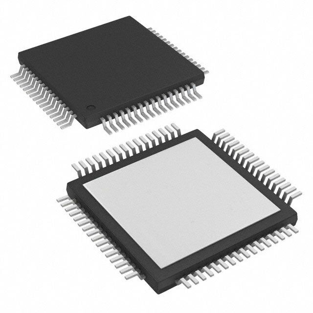
| 供应商器件封装 | 64-HTQFP(10x10) |
| 其它名称 | 296-14643-1 |
| 制造商产品页 | http://www.ti.com/general/docs/suppproductinfo.tsp?distId=10&orderablePartNumber=ADS1605IPAPT |
| 包装 | Digi-Reel® |
| 安装类型 | 表面贴装 |
| 封装/外壳 | 64-TQFP 裸露焊盘 |
| 工作温度 | -40°C ~ 85°C |
| 数据接口 | 并联 |
| 标准包装 | 1 |
| 特性 | - |
| 电压源 | 模拟和数字 |
| 视频文件 | http://www.digikey.cn/classic/video.aspx?PlayerID=1364138032001&width=640&height=455&videoID=44659313001 |
| 转换器数 | 1 |
| 输入数和类型 | 1 个差分,双极 |
| 配用 | /product-detail/zh/ADS1605EVM/296-18363-ND/809659 |
| 采样率(每秒) | 5M,10M |


- 商务部:美国ITC正式对集成电路等产品启动337调查
- 曝三星4nm工艺存在良率问题 高通将骁龙8 Gen1或转产台积电
- 太阳诱电将投资9.5亿元在常州建新厂生产MLCC 预计2023年完工
- 英特尔发布欧洲新工厂建设计划 深化IDM 2.0 战略
- 台积电先进制程称霸业界 有大客户加持明年业绩稳了
- 达到5530亿美元!SIA预计今年全球半导体销售额将创下新高
- 英特尔拟将自动驾驶子公司Mobileye上市 估值或超500亿美元
- 三星加码芯片和SET,合并消费电子和移动部门,撤换高东真等 CEO
- 三星电子宣布重大人事变动 还合并消费电子和移动部门
- 海关总署:前11个月进口集成电路产品价值2.52万亿元 增长14.8%


PDF Datasheet 数据手册内容提取
ADS1605 ADS1606 SBAS274H − MARCH 2003 − REVISED MAY 2007 16-Bit, 5MSPS Analog-to-Digital Converter FEATURES DESCRIPTION (cid:1) The ADS1605 and ADS1606 are high-speed, high-pre- Data Rate: 5MSPS (10MSPS in 2X Mode) (cid:1) cision, delta-sigma analog-to-digital converters (ADCs) Signal-to-Noise Ratio: 88dB with 16-bit resolution. The data rate is 5 mega-samples (cid:1) Total Harmonic Distortion: −99dB per second (MSPS), the bandwidth (−3dB) is 2.45MHz, (cid:1) Spurious-Free Dynamic Range: 101dB and passband ripple is less than ±0.0025dB (to (cid:1) Linear Phase with 2.45MHz Bandwidth 2.2MHz). Both devices offer the same outstanding per- (cid:1) Passband Ripple: ±0.0025dB formance at these speeds with a signal-to-noise ratio up (cid:1) to 88dB, total harmonic distortion down to −99dB, and Selectable On-Chip Reference a spurious-free dynamic range up to 101dB. For even (cid:1) Directly Connects to TMS320C6000 DSPs higher-speed operation, the data rate can be doubled to (cid:1) Easily Upgradable to 18 Bits with the 10MSPS in 2X mode. The ADS1606 includes an adjust- ADS1625 and ADS1626 able first-in first-out buffer (FIFO) for the output data. (cid:1) Adjustable Power Dissipation: 315 to 570mW The input signal is measured against a voltage refer- (cid:1) ence that can be generated on-chip or supplied exter- Power Down Mode (cid:1) nally. The digital output data are provided over a simple Supplies:Analog +5V parallel interface that easily connects to digital signal Digital +3V processors (DSPs). An out-of-range monitor reports Digital I/O +2.7V to +5.25V when the input range has been exceeded. The ADS1605/6 operate from a +5V analog supply (AVDD) APPLICATIONS and +3V digital supply (DVDD). The digital I/O supply (cid:1) (IOVDD) operates from +2.7 to +5.25V, enabling the Scientific Instruments digital interface to support a range of logic families. The (cid:1) Automated Test Equipment analog power dissipation is set by an external resistor (cid:1) Data Acquisition and can be reduced when operating at slower speeds. (cid:1) Medical Imaging A power down mode, activated by a digital I/O pin, shuts (cid:1) down all circuitry. The ADS1605/6 are offered in a Vibration Analysis TQFP-64 package using TI PowerPAD technology. The ADS1605 and ADS1606, along with their 18-bit counterparts, the ADS1625 and ADS1626, are well suited for the demanding measurement requirements of scientific instrumentation, automated test equip- ment, data acquisition, and medical imaging. VREFP VREFN VMID RBIAS VCAP AVDD DVDD IOVDD PD Reference and Bias Circuits REFEN RESET CLK CS AINP (cid:1)(cid:2) Digital I/O 2XMODE Interface RD Modulator Filter AINN DRDY OTR ADS1606 Only DOUT[15:0] FIFO ADS1605 ADS1606 FIFO_LEV[2:0] AGND DGND Please be aware that an important notice concerning availability, standard warranty, and use in critical applications of TexasInstruments semiconductor products and disclaimers thereto appears at the end of this data sheet. PowerPAD is a trademark of Texas Instruments. All other trademarks are the property of their respective owners. (cid:1)(cid:2)(cid:3)(cid:4)(cid:5)(cid:6)(cid:7)(cid:8)(cid:3)(cid:9) (cid:4)(cid:10)(cid:7)(cid:10) (cid:11)(cid:12)(cid:13)(cid:14)(cid:15)(cid:16)(cid:17)(cid:18)(cid:11)(cid:14)(cid:12) (cid:11)(cid:19) (cid:20)(cid:21)(cid:15)(cid:15)(cid:22)(cid:12)(cid:18) (cid:17)(cid:19) (cid:14)(cid:13) (cid:23)(cid:21)(cid:24)(cid:25)(cid:11)(cid:20)(cid:17)(cid:18)(cid:11)(cid:14)(cid:12) (cid:26)(cid:17)(cid:18)(cid:22)(cid:27) (cid:1)(cid:15)(cid:14)(cid:26)(cid:21)(cid:20)(cid:18)(cid:19) Copyright 2003−2007, Texas Instruments Incorporated (cid:20)(cid:14)(cid:12)(cid:13)(cid:14)(cid:15)(cid:16) (cid:18)(cid:14) (cid:19)(cid:23)(cid:22)(cid:20)(cid:11)(cid:13)(cid:11)(cid:20)(cid:17)(cid:18)(cid:11)(cid:14)(cid:12)(cid:19) (cid:23)(cid:22)(cid:15) (cid:18)(cid:28)(cid:22) (cid:18)(cid:22)(cid:15)(cid:16)(cid:19) (cid:14)(cid:13) (cid:7)(cid:22)(cid:29)(cid:17)(cid:19) (cid:8)(cid:12)(cid:19)(cid:18)(cid:15)(cid:21)(cid:16)(cid:22)(cid:12)(cid:18)(cid:19) (cid:19)(cid:18)(cid:17)(cid:12)(cid:26)(cid:17)(cid:15)(cid:26) (cid:30)(cid:17)(cid:15)(cid:15)(cid:17)(cid:12)(cid:18)(cid:31)(cid:27) (cid:1)(cid:15)(cid:14)(cid:26)(cid:21)(cid:20)(cid:18)(cid:11)(cid:14)(cid:12) (cid:23)(cid:15)(cid:14)(cid:20)(cid:22)(cid:19)(cid:19)(cid:11)(cid:12)! (cid:26)(cid:14)(cid:22)(cid:19) (cid:12)(cid:14)(cid:18) (cid:12)(cid:22)(cid:20)(cid:22)(cid:19)(cid:19)(cid:17)(cid:15)(cid:11)(cid:25)(cid:31) (cid:11)(cid:12)(cid:20)(cid:25)(cid:21)(cid:26)(cid:22) (cid:18)(cid:22)(cid:19)(cid:18)(cid:11)(cid:12)! (cid:14)(cid:13) (cid:17)(cid:25)(cid:25) (cid:23)(cid:17)(cid:15)(cid:17)(cid:16)(cid:22)(cid:18)(cid:22)(cid:15)(cid:19)(cid:27) www.ti.com
(cid:10)(cid:4)"#$%& (cid:10)(cid:4)"#$%$ www.ti.com SBAS274H − MARCH 2003 − REVISED MAY 2007 ORDERING INFORMATION(1) SPECIFIED PACKAGE PACKAGE ORDERING TRANSPORT PRODUCT PACKAGE−LEAD TEMPERATURE DESIGNATOR MARKING NUMBER MEDIA, QUANTITY RANGE ADS1605IPAPT Tape and Reel, 250 AADDSS11660055 HHTTQQFFPP−−6644 PPAAPP −−4400°°CC ttoo ++8855°°CC AADDSS11660055II ADS1605IPAPR Tape and Reel, 1000 ADS1606IPAPT Tape and Reel, 250 AADDSS11660066 HHTTQQFFPP−−6644 PPAAPP −−4400°°CC ttoo ++8855°°CC AADDSS11660066II ADS1606IPAPR Tape and Reel, 1000 (1)For the most current package and ordering information, see the Package Option Addendum at the end of this data sheet, or see the TI web site at www.ti.com. ABSOLUTE MAXIMUM RATINGS PRODUCT FAMILY over operating free-air temperature range unless otherwise noted(1) PRODUCT RESOLUTION DATA RATE FIFO? ADS1605, ADS1606 UNIT ADS1605 16 Bits 5.0MSPS No AVDD to AGND −0.3 to +6 V ADS1606 16 Bits 5.0MSPS Yes DVDD to DGND −0.3 to +3.6 V ADS1625 18 Bits 1.25MSPS No IOVDD to DGND −0.3 to +6 V ADS1626 18 Bits 1.25MSPS Yes AGND to DGND −0.3 to +0.3 V Input Current 100mA, Momentary Input Current 10mA, Continuous This integrated circuit can be damaged by ESD. Texas Instruments recommends that all integrated circuits be Analog I/O to AGND −0.3 to AVDD + 0.3 V handled with appropriate precautions. Failure to observe Digital I/O to DGND −0.3 to IOVDD + 0.3 V proper handling and installation procedures can cause damage. Maximum Junction Temperature +150 °C ESD damage can range from subtle performance degradation to Operating Temperature Range −40 to +105 °C complete device failure. Precision integrated circuits may be more Storage Temperature Range −60 to +150 °C susceptible to damage because very small parametric changes could cause the device not to meet its published specifications. Lead Temperature (soldering, 10s) +260 °C (1)Stresses above these ratings may cause permanent damage. Exposure to absolute maximum conditions for extended periods may degrade device reliability. These are stress ratings only, and functional operation of the device at these or any other conditions beyond those specified is not implied. 2
(cid:10)(cid:4)"#$%& (cid:10)(cid:4)"#$%$ www.ti.com SBAS274H − MARCH 2003 − REVISED MAY 2007 ELECTRICAL CHARACTERISTICS All specifications at −40°C to +85°C, AVDD = 5V, DVDD = IOVDD = 3V, fCLK = 40MHz, External VREF = +3V, 2XMODE = low, VCM = 2.0V, FIFO disabled, and RBIAS = 37kΩ, unless otherwise noted. PARAMETER TEST CONDITIONS MIN TYP MAX UNIT Analog Input 0dBFS ±1.467VREF V DDiiffffeerreennttiiaall iinnppuutt vvoollttaaggee ((VVIINN)) −2dBFS ±1.165VREF V ((AAIINNPP −− AAIINNNN)) −6dBFS ±0.735VREF V −20dBFS ±0.147VREF V Common-mode input voltage (VCM) 2.0 V (AINP + AINN) / 2 AAbbssoolluuttee iinnppuutt vvoollttaaggee 0dBFS −0.1 4.7 V ((AAIINNPP oorr AAIINNNN wwiitthh rreessppeecctt ttoo AAGGNNDD)) −2dBFS input and smaller 0.1 4.2 V Dynamic Specifications (cid:1) (cid:2) f Data rate 5.0 CLK MSPS 40MHz fIN = 100kHz, −2dBFS 88 dB fIN = 100kHz, −6dBFS 84 dB fIN = 100kHz, −20dBFS 62 70 dB fIN = 500kHz, −2dBFS 86 dB SSiiggnnaall--ttoo--nnooiissee rraattiioo ((SSNNRR)) fIN = 500kHz, −6dBFS 83 dB fIN = 500kHz, −20dBFS 69 dB fIN = 2MHz, −2dBFS 84 dB fIN = 2MHz, −6dBFS 82 dB fIN = 2MHz, −20dBFS 69 dB fIN = 100kHz, −2dBFS −93 dB fIN = 100kHz, −6dBFS −99 dB fIN = 100kHz, −20dBFS −94 −85 dB fIN = 500kHz, −2dBFS −94 dB TToottaall hhaarrmmoonniicc ddiissttoorrttiioonn ((TTHHDD)) fIN = 500kHz, −6dBFS −97 dB fIN = 500kHz, −20dBFS −93 dB fIN = 2MHz, −2dBFS −98 dB fIN = 2MHz, −6dBFS −101 dB fIN = 2MHz, −20dBFS −92 dB fIN = 100kHz, −2dBFS 86 dB fIN = 100kHz, −6dBFS 84 dB fIN = 100kHz, −20dBFS 62 70 dB fIN = 500kHz, −2dBFS 86 dB SSiiggnnaall--ttoo--nnooiissee aanndd ddiissttoorrttiioonn ((SSIINNAADD)) fIN = 500kHz, −6dBFS 83 dB fIN = 500kHz, −20dBFS 69 dB fIN = 2MHz, −2dBFS 84 dB fIN = 2MHz, −6dBFS 82 dB fIN = 2MHz, −20dBFS 69 dB 3
(cid:10)(cid:4)"#$%& (cid:10)(cid:4)"#$%$ www.ti.com SBAS274H − MARCH 2003 − REVISED MAY 2007 ELECTRICAL CHARACTERISTICS (continued) All specifications at −40°C to +85°C, AVDD = 5V, DVDD = IOVDD = 3V, fCLK = 40MHz, External VREF = +3V, 2XMODE = low, VCM = 2.0V, FIFO disabled, and RBIAS = 37kΩ, unless otherwise noted. PARAMETER TEST CONDITIONS MIN TYP MAX UNIT fIN = 100kHz, −2dBFS 96 dB fIN = 100kHz, −6dBFS 101 dB fIN = 100kHz, −20dBFS 85 96 dB fIN = 500kHz, −2dBFS 95 dB SSppuurriioouuss ffrreeee ddyynnaammiicc rraannggee ((SSFFDDRR)) fIN = 500kHz, −6dBFS 100 dB fIN = 500kHz, −20dBFS 95 dB fIN = 2MHz, −2dBFS 102 dB fIN = 2MHz, −6dBFS 105 dB fIN = 2MHz, −20dBFS 96 dB ff11 == 11..9999MMHHzz,, −−66ddBBFFSS IInntteerrmmoodduullaattiioonn ddiissttoorrttiioonn ((IIMMDD)) −−9944 ddBB ff2 == 22..0000MMHHzz,, −−66ddBBFFSS Aperture delay 4 ns Digital Filter Characteristics (cid:1) (cid:2) f Passband 0 CLK MHz 2.2 40MHz Passband ripple ±0.0025 dB (cid:1) (cid:2) f −0.1dB attenuation 2.3 CLK MHz 40MHz PPaassssbbaanndd ttrraannssiittiioonn (cid:1) (cid:2) f −3.0dB attenuation 2.45 CLK MHz 40MHz (cid:1) (cid:2) (cid:1) (cid:2) f f Stop band 2.8 CLK 37.2 CLK MHz 40MHz 40MHz Stop band attenuation 72 dB (cid:1) (cid:2) Group delay 5.2 40MHz µs f CLK (cid:1) (cid:2) Settling time To ±0.001% 9.4 40MHz µs f CLK Static Specifications Resolution 16 Bits No missing codes 16 Bits Input-referred noise 1.0 LSB, rms Integral nonlinearity −1.5dBFS signal ±0.75 LSB Differential nonlinearity ±0.25 LSB Offset error 0.05 %FSR Offset error drift 1 ppmFSR/°C Gain error 0.25 % Gain error drift Excluding reference drift 10 ppm/°C Common-mode rejection At dc 75 dB Power-supply rejection At dc 65 dB 4
(cid:10)(cid:4)"#$%& (cid:10)(cid:4)"#$%$ www.ti.com SBAS274H − MARCH 2003 − REVISED MAY 2007 ELECTRICAL CHARACTERISTICS (continued) All specifications at −40°C to +85°C, AVDD = 5V, DVDD = IOVDD = 3V, fCLK = 40MHz, External VREF = +3V, 2XMODE = low, VCM = 2.0V, FIFO disabled, and RBIAS = 37kΩ, unless otherwise noted. PARAMETER TEST CONDITIONS MIN TYP MAX UNIT Voltage Reference(1) VREF = (VREFP − VREFN) 2.5 3.0 3.2 V VREFP 3.75 4.0 4.25 V VREFN 0.75 1.0 1.25 V VMID 2.3 2.5 2.8 V VREF drift Internal reference (REFEN = low) 50 ppm/°C Startup time Internal reference (REFEN = low) 15 ms Clock Input Frequency (fCLK) 40 50 MHz Duty Cycle fCLK = 40MHz 45 55 % Digital Input/Output VIH 0.7 IOVDD IOVDD V VIL DGND 0.3 IOVDD V VOH IOH = 50µA IOVDD − 0.5 V VOL IOL = 50µA DGND +0.5 V Input leakage DGND < VDIGIN < IOVDD ±10 µA Power-Supply Requirements AVDD 4.75 5.25 V DVDD 2.7 3.3 V IOVDD 2.7 5.25 V REFEN = low 110 135 mA AAVVDDDD ccuurrrreenntt ((IIAAVVDDDD)) REFEN = high 85 105 mA DVDD current (IDVDD) 45 55 mA IOVDD current (IIOVDD) IOVDD = 3V 4 6 mA AVDD = 5V, DVDD = 3V, IOVDD = 3V, 570 710 mW PPoowweerr ddiissssiippaattiioonn REFEN = high PD = low, CLK disabled 5 mW Temperature Range Specified −40 +85 °C Operating −40 +105 °C Storage −60 +150 °C Thermal Resistance, θJA PPoowweerrPPAADDssoollddeerreedd ttoo PPCCBB wwiitthh 22oozz.. 25 °C/W θJC ttrraaccee aanndd ccooppppeerr ppaadd.. 0.5 °C/W (1)The specification limits for VREF, VREFP, VREFN, and VMID apply when using the internal or an external reference. The internal reference voltages are bounded by the limits shown. When using an external reference, the limits indicate the allowable voltages that can be applied to the reference pins. 5
(cid:10)(cid:4)"#$%& (cid:10)(cid:4)"#$%$ www.ti.com SBAS274H − MARCH 2003 − REVISED MAY 2007 DEFINITIONS Absolute Input Voltage Intermodulation Distortion (IMD) Absolute input voltage, given in volts, is the voltage of IMD, given in dB, is measured while applying two input each analog input (AINN or AINP) with respect to signals of the same magnitude, but with slightly different AGND. frequencies. It is calculated as the difference between Aperture Delay the rms amplitude of the input signal to the rms ampli- tude of the peak spurious signal. Aperture delay is the delay between the rising edge of Offset Error CLK and the sampling of the input signal. Common-Mode Input Voltage Offset Error, given in % of FSR, is the output reading when the differential input is zero. Common-mode input voltage (V ) is the average volt- CM Offset Error Drift age of the analog inputs: (AINP(cid:3)AINN) Offset error drift, given in ppm of FSR/(cid:2)C, is the drift over temperature of the offset error. The offset error is 2 specified as the larger of the drift from ambient (T = Differential Input Voltage 25(cid:2)C) to the minimum or maximum operating tempera- Differential input voltage (V ) is the voltage difference tures. IN between the analog inputs: (AINP−AINN). Signal-to-Noise Ratio (SNR) Differential Nonlinearity (DNL) SNR, given in dB, is the ratio of the rms value of the in- DNL, given in least-significant bits of the output code put signal to the sum of all the frequency components (LSB), is the maximum deviation of the output code step below fCLK/2 (the Nyquist frequency) excluding the first sizes from the ideal value of 1LSB. six harmonics of the input signal and the dc component. Full-Scale Range (FSR) Signal-to-Noise and Distortion (SINAD) FSR is the difference between the maximum and mini- SINAD, given in dB, is the ratio of the rms value of the mum measurable input signals. FSR = 2 × 1.467V . input signal to the sum of all the frequency components REF Gain Error below fCLK/2 (the Nyquist frequency) including the har- monics of the input signal but excluding the dc compo- Gain error, given in %, is the error of the full-scale input nent. signal with respect to the ideal value. Spurious-Free Dynamic Range (SFDR) Gain Error Drift SFDR, given in dB, is the difference between the rms Gain error drift, given in ppm/(cid:2)C, is the drift over tem- amplitude of the input signal to the rms amplitude of the perature of the gain error. The gain error is specified as peak spurious signal. the larger of the drift from ambient (T = 25(cid:2)C) to the Total Harmonic Distortion (THD) minimum or maximum operating temperatures. Integral Nonlinearity (INL) THD, given in dB, is the ratio of the sum of the rms value of the first six harmonics of the input signal to the rms INL, given in least-significant bits of the output code value of the input signal. (LSB), is the maximum deviation of the output codes from a best fit line. 6
(cid:10)(cid:4)"#$%& (cid:10)(cid:4)"#$%$ www.ti.com SBAS274H − MARCH 2003 − REVISED MAY 2007 PIN ASSIGNMENTS VREFP VREFP VMID VREFN VREFN VCAP AVDD AGND CLK AGND DGND IOVDD DVDD DGND NC NC 64 63 62 61 60 59 58 57 56 55 54 53 52 51 50 49 AGND 1 ADS1605 48 FIFO_LEV[2](ADS1606Only) AVDD 2 ADS1606 47 FIFO_LEV[1](ADS1606Only) AGND 3 46 FIFO_LEV[0](ADS1606Only) AINN 4 45 NC AINP 5 44 DOUT[15] AGND 6 43 DOUT[14] TQFP PACKAGE AVDD 7 42 DOUT[13] (TOP VIEW) RBIAS 8 41 DOUT[12] PowerPADTM AGND 9 40 DOUT[11] AVDD 10 39 DOUT[10] AGND 11 38 DOUT[9] AVDD 12 37 DOUT[8] REFEN 13 36 DOUT[7] NC 14 35 DOUT[6] 2XMODE 15 34 DOUT[5] NC 16 33 DOUT[4] 17 18 19 20 21 22 23 24 25 26 27 28 29 30 31 32 PD DVDD DGND RESET CS RD OTR DRDY DGND DVDD NC NC DOUT[0] DOUT[1] DOUT[2] DOUT[3] Terminal Functions TERMINAL NAME NO. TYPE DESCRIPTION AGND 1, 3, 6, 9, 11, 55, 57 Analog Analog ground AVDD 2, 7, 10, 12, 58 Analog Analog supply AINN 4 Analog input Negative analog input AINP 5 Analog input Positive analog input RBIAS 8 Analog Terminal for external analog bias setting resistor REFEN 13 Digital input: active low Internal reference enable. Internal pull-down resistor of 170kΩ to DGND. NC 14,16, 27, 28, 45, 50 Not connected These terminals are not connected within the ADS1605/6 and must be left unconnected. 2XMODE 15 Digital input Digital filter decimation rate. Internal pull-down resistor of 170kΩ to DGND. PD 17 Digital input: active low Power down all circuitry. Internal pull-up resistor of 170kΩ to DGND. DVDD 18, 26, 52 Digital Digital supply DGND 19, 25, 51, 54 Digital Digital ground RESET 20 Digital input: active low Reset digital filter CS 21 Digital input: active low Chip select RD 22 Digital input: active low Read enable OTR 23 Digital output Analog inputs out of range DRDY 24 Digital output: active low Data ready on falling edge DOUT [15:0] 29−44 Digital output Data output. DOUT[15] is the MSB and DOUT[0] is the LSB. FIFO_LEV[2:0] 46−48 Digital input FIFO level (for the ADS1606 only). FIFO_LEV[2] is MSB. NOTE: These terminals must be left disconnected on the ADS1605. IOVDD 53 Digital Digital I/O supply CLK 56 Digital input Clock input VCAP 59 Analog Terminal for external bypass capacitor connection to internal bias voltage VREFN 60, 61 Analog Negative reference voltage VMID 62 Analog Midpoint voltage VREFP 63, 64 Analog Positive reference voltage 7
(cid:10)(cid:4)"#$%& (cid:10)(cid:4)"#$%$ www.ti.com SBAS274H − MARCH 2003 − REVISED MAY 2007 PARAMETER MEASUREMENT INFORMATION t1 t2 CLK t 2 t 3 t t DRDY 4 4 t 6 t 5 DOUT[15:0] DataN DataN+1 DataN+2 NOTE:CSandRDtiedlow. Figure 1. Data Retrieval Timing (ADS1605, ADS1606 with FIFO Disabled) RD,CS t t 7 8 DOUT[15:0] Figure 2. DOUT Inactive/Active Timing (ADS1605, ADS1606 with FIFO Disabled) TIMING REQUIREMENTS FOR FIGURE 1 AND FIGURE 2 SYMBOL DESCRIPTION MIN TYP MAX UNIT t1 CLK period (1/fCLK) 20 25 1000 ns 1/t1 fCLK 1 40 50 MHz t2 CLK pulse width, high or low 10 ns t3 Rising edge of CLK to DRDY low 10 ns t4 DRDY pulse width high or low 4 t1 ns t5 Falling edge of DRDY to data invalid 10 ns t6 Falling edge of DRDY to data valid 15 ns t7 Rising edge of RD and/or CS inactive (high) to DOUT high impedance 15 ns t8 Falling edge of RD and/or CS active (low) to DOUT active. 15 ns NOTE: DOUT[15:0] and DRDY load = 10pF. 8
(cid:10)(cid:4)"#$%& (cid:10)(cid:4)"#$%$ www.ti.com SBAS274H − MARCH 2003 − REVISED MAY 2007 CLK t 11 t RESET 9 t t 10 12 DRDY t 3 DOUT[15:0] Settled Data NOTE:CSandRDtiedlow. Figure 3. Reset TIming (ADS1605, ADS1606 with FIFO Disabled) TIMING REQUIREMENTS FOR FIGURE 3 SYMBOL DESCRIPTION MIN TYP MAX UNIT t3 Rising edge of CLK to DRDY low 10 ns t9 RESET pulse width 50 ns t10 Delay from RESET active (low) to DRDY forced high and DOUT forced low 9 ns t11 RESET rising edge to falling edge of CLK −5 10 ns DRDY t12 Delay from DOUT active to valid DOUT (settling to 0.001%) 47 Cycles NOTE: DOUT[15:0] and DRDY load = 10pF. 9
(cid:10)(cid:4)"#$%& (cid:10)(cid:4)"#$%$ www.ti.com SBAS274H − MARCH 2003 − REVISED MAY 2007 t1 t2 CLK t t 2 13 t 14 DRDY t t 15 16 CS(1) t t 21 17 t RD 20 t18 t19 DOUT[15:0] D1 D2 DL(2) (1)CSmaybetiedlow. (2)Thenumberofdatareadings(DL)issetbytheFIFOlevel. Figure 4. Data Retrieval Timing (ADS1606 with FIFO Enabled) RD,CS t t 7 8 DOUT[15:0] Figure 5. DOUT Inactive/Active Timing (ADS1606 with FIFO Enabled) TIMING REQUIREMENTS FOR FIGURE 4 AND FIGURE 5 SYMBOL DESCRIPTION MIN TYP MAX UNIT t1 CLK period (1/fCLK) 20 25 1000 ns t2 CLK pulse width, high or low 10 ns t7 Rising edge of RD and/or CS inactive (high) to DOUT high impedance 7 15 ns t8 Falling edge of RD and/or CS active (low) to DOUT active. 7 15 ns t13 Rising edge of CLK to DRDY high 12 ns CLK t14 DRDY period 8 ×FIFO Level(1) Cycles CLK t15 DRDY positive pulse width 1 Cycles t16 RD high hold time after DRDY goes low 0 ns t17 CS low before RD goes low 0 ns t18 RD negative pulse width 10 ns t19 RD positive pulse width 10 ns CLK t20 RD high before DRDY toggles 2 Cycles t21 RD high before CS goes high 0 ns NOTE: DOUT[15:0] and DRDY load = 10pF. (1)See FIFO section for more details. 10
(cid:10)(cid:4)"#$%& (cid:10)(cid:4)"#$%$ www.ti.com SBAS274H − MARCH 2003 − REVISED MAY 2007 CLK t 11 t RESET 9 t 26 t 25 DRDY t 23 t RD 24 Figure 6. Reset Timing (ADS1606 with FIFO Enabled) TIMING REQUIREMENTS FOR FIGURE 6 SYMBOL DESCRIPTION MIN TYP MAX UNIT t9 RESET pulse width 50 ns t11 RESET rising edge to falling edge of CLK −5 10 ns CLK t23 RD pulse low after RESET goes high 8 Cycles CLK t24 RD pulse high before first DRDY pulse after RESET goes high 8 Cycles CLK t25 DRDY low after RESET goes low 8 × (FIFO level + 1) Cycles DRDY t26 Delay from RESET high to valid DOUT (settling to 0.001%) See Table 4 Cycles 11
(cid:10)(cid:4)"#$%& (cid:10)(cid:4)"#$%$ www.ti.com SBAS274H − MARCH 2003 − REVISED MAY 2007 TYPICAL CHARACTERISTICS All specifications at TA = 25°C, AVDD = 5V, DVDD = IOVDD = 3V, fCLK = 40MHz, External VREF = +3V, 2XMODE = low, VCM = 2.0V, and RBIAS = 37kΩ, unless otherwise noted. SPECTRALRESPONSE SPECTRALRESPONSE 0 0 f =100kHz,−2dBFS f =100kHz,−6dBFS −20 IN −20 IN SNR=88dB SNR=84dB −40 THD=−93dB −40 THD=−99dB SFDR=96dB SFDR=101dB dB) −60 dB) −60 ( ( e e ud −80 ud −80 plit plit m −100 m −100 A A −120 −120 −140 −140 −160 −160 0 0.5 1.0 1.5 2.0 2.5 0 0.5 1.0 1.5 2.0 2.5 Frequency(MHz) Frequency(MHz) SPECTRALRESPONSE SPECTRALRESPONSE 0 0 −20 fSINN=R5=080k6HdBz,−2dBFS −20 fSINN=R5=008k3HdBz,−6dBFS −40 TSHFDDR==−9977ddBB −40 TSHFDDR==−110036ddBB dB) −60 dB) −60 ( ( e e ud −80 ud −80 plit plit m −100 m −100 A A −120 −120 −140 −140 −160 −160 0 0.5 1.0 1.5 2.0 2.5 0 0.5 1.0 1.5 2.0 2.5 Frequency(MHz) Frequency(MHz) SPECTRALRESPONSE SPECTRALRESPONSE 0 0 f =2MHz,−2dBFS f =2MHz,−6dBFS −20 SINNR=84dB −20 SINNR=82dB THD=−98dB THD=−101dB −40 −40 SFDR=102dB SFDR=105dB dB) −60 dB) −60 ( ( e e ud −80 ud −80 plit plit m −100 m −100 A A −120 −120 −140 −140 −160 −160 0 0.5 1.0 1.5 2.0 2.5 0 0.5 1.0 1.5 2.0 2.5 Frequency(MHz) Frequency(MHz) 12
(cid:10)(cid:4)"#$%& (cid:10)(cid:4)"#$%$ www.ti.com SBAS274H − MARCH 2003 − REVISED MAY 2007 TYPICAL CHARACTERISTICS (continued) All specifications at TA = 25°C, AVDD = 5V, DVDD = IOVDD = 3V, fCLK = 40MHz, External VREF = +3V, 2XMODE = low, VCM = 2.0V, and RBIAS = 37kΩ, unless otherwise noted. NOISEHISTOGRAM INTERMODULATIONRESPONSE 18k 0 16k VIN=0V −20 ffIINN12==12..9090MMHHzz B) IMD=−94dB 14k (d −40 y Occurrences112086kkkk SpectralDensit−−−1680000 4k wer−120 o 2k P−140 0 −160 −5 −4 −3 −2 −1 0 1 2 3 4 5 1.95 1.96 1.97 1.98 1.99 2.00 2.01 2.02 2.03 2.04 2.05 OutputCode(LSB) Frequency(MHz) SIGNAL−TO−NOISERATIO, TOTALHARMONICDISTORTION, ANDSPURIOUS−FREEDYNAMICRANGE SIGNAL−TO−NOISERATIO vsINPUTSIGNALAMPLITUDE vsINPUTFREQUENCY 110 90 V =−2dBFS 100 IN dB) 90 85 ( DR 80 SFDR 80 VIN=−6dBFS SF 70 B) and 60 R(d 75 THD, 50 THD SN 70 VIN=−20dBFS R, 40 SNR N S 30 f =100kHz 65 20 IN 10 60 −70 −60 −50 −40 −30 −20 −10 0 0.001 0.01 0.1 1 10 InputSignalAmplitude,V (dB) InputFrequency,f (MHz) IN IN TOTALHARMONICDISTORTION SPURIOUS−FREEDYNAMICRANGE vsINPUTFREQUENCY vsINPUTFREQUENCY −85 110 108 −90 106 VIN=−20dBFS 104 VIN=−6dBFS THD(dB)−−19050 VIN=−2dBFS SFDR(dB) 11009208 V =−20dBFS VIN=−2dBFS IN 96 V =−6dBFS −105 IN 94 92 −110 90 0.001 0.01 0.1 1 10 0.001 0.01 0.1 1 10 InputFrequency,f (MHz) InputFrequency,f (MHz) IN IN 13
(cid:10)(cid:4)"#$%& (cid:10)(cid:4)"#$%$ www.ti.com SBAS274H − MARCH 2003 − REVISED MAY 2007 TYPICAL CHARACTERISTICS (continued) All specifications at TA = 25°C, AVDD = 5V, DVDD = IOVDD = 3V, fCLK = 40MHz, External VREF = +3V, 2XMODE = low, VCM = 2.0V, and RBIAS = 37kΩ, unless otherwise noted. SIGNAL−TO−NOISERATIO TOTALHARMONICDISTORTION vsINPUTCOMMON−MODEVOLTAGE vsINPUTCOMMON−MODEVOLTAGE 89 −65 87 −75 V =−2dBFS IN 85 −85 V =−2dBFS R(dB) 83 VIN=−6dBFS D(dB) −95 VIN =−6dBFS SN 81 TH −105 IN 79 −115 77 −125 f =100kHz f =100kHz IN IN 75 −135 1.5 1.7 1.9 2.1 2.3 2.5 1.5 1.7 1.9 2.1 2.3 2.5 InputCommon−ModeVoltage,V (V) InputCommon−ModeVoltage,V (V) CM CM SPURIOUS−FREEDYNAMICRANGE SIGNAL−TO−NOISERATIO vsINPUTCOMMON−MODEVOLTAGE vsCLKFREQUENCY 105 90 VIN=−6dBFS 85 RBIAS=30kΩ 100 80 95 V =−2dBFS 75 SFDR(dB) 988050 IN SNR(dB) 766050 RBIAS=R3B7IAkSΩR=B4IA5Sk=Ω50kΩ 55 75 RBIAS=60kΩ 50 70 f =100kHz 45 fIN=100kHz,−6dBFS IN 65 40 1.5 1.7 1.9 2.1 2.3 2.5 10 20 30 40 50 60 InputCommon−ModeVoltage,V (V) CLKFrequency,f (MHz) CM CLK TOTALHARMONICDISTORTION SPURIOUS−FREEDYNAMICRANGE vsCLKFREQUENCY vsCLKFREQUENCY −65 110 −70 fIN=100kHz,−6dBFS 105 fIN=100kHz,−6dBFS −75 RBIAS=60kΩ RBIAS=30kΩ THD(dB) −−−889050 RBIASR=BIA4S5=kΩ50kΩ SFDR(dB)1099050 RBIAS=R45kΩ=50kΩ RBIAS=37kΩ BIAS −95 R =37kΩ 85 R =60kΩ BIAS BIAS −100 80 R =30kΩ BIAS −105 75 10 20 30 40 50 60 10 20 30 40 50 60 CLKFrequency,f (MHz) CLKFrequency,f (MHz) CLK CLK 14
(cid:10)(cid:4)"#$%& (cid:10)(cid:4)"#$%$ www.ti.com SBAS274H − MARCH 2003 − REVISED MAY 2007 TYPICAL CHARACTERISTICS (continued) All specifications at TA = 25°C, AVDD = 5V, DVDD = IOVDD = 3V, fCLK = 40MHz, External VREF = +3V, 2XMODE = low, VCM = 2.0V, and RBIAS = 37kΩ, unless otherwise noted. SIGNAL−TO−NOISERATIO TOTALHARMONICDISTORTION vsTEMPERATURE vsTEMPERATURE 100 −85 90 VIN=−2dBFS −90 V =−20dBFS IN R(dB) 80 VIN=−6dBFS D(dB) −95 VIN=−2dBFS N H S 70 T−100 VIN=−20dBFS VIN=−6dBFS 60 −105 f =100kHz f =100kHz IN IN 50 −110 −40 −15 10 35 60 85 −40 −15 10 35 60 85 Temperature((cid:2)C) Temperature((cid:2)C) SPURIOUS−FREEDYNAMICRANGE POWER−SUPPLYCURRENT vsTEMPERATURE vsTEMPERATURE 110 130 120 IAVDD(REFEN=low) 105 110 V =−6dBFS 100 B) 100 IN mA) 90 IAVDD(REFEN=high) R(d VIN=−20dBFS nt( 80 D e SF 95 Curr 70 VIN=−2dBFS 60 IDVDD+IIOVDD 90 50 fIN=100kHz 40 R =37kΩ,f =40MHz DVDD=IOVDD=3V 85 30 BIAS CLK −40 −15 10 35 60 85 −40 −15 10 35 60 85 Temperature((cid:2)C) Temperature((cid:2)C) SUPPLYCURRENTvsCLKFREQUENCY ANALOGSUPPLYCURRENTvsRBIAS 100 140 I (R =37kΩ) 130 AVDD BIAS 80 mA) 120 A) ( urrent(m 60 IAVDD(RBIAS=60kΩ) ent,IAVDD111000 REFEN=low plyC 40 Curr 90 p g 80 u I +I o S DVDD IOVDD al n 70 20 A REFEN=high 60 AVDD=5V,DVDD=IOVDD=3V,REFEN=High 0 50 10 20 30 40 50 30 35 40 45 50 55 60 CLKFrequency,fCLK(MHz) RBIAS(kΩ) 15
(cid:10)(cid:4)"#$%& (cid:10)(cid:4)"#$%$ www.ti.com SBAS274H − MARCH 2003 − REVISED MAY 2007 TYPICAL CHARACTERISTICS (continued) All specifications at TA = 25°C, AVDD = 5V, DVDD = IOVDD = 3V, fCLK = 40MHz, External VREF = +3V, 2XMODE = low, VCM = 2.0V, and RBIAS = 37kΩ, unless otherwise noted. INTEGRALNONLINEARITY DIFFERENTIALNONLINEARITY 1.0 0.5 f =100Hz,−1.5dBFS f =100Hz,−1.5dBFS 0.8 IN 0.4 IN 0.6 0.3 0.4 0.2 INL(LSB) −00..202 DNL(LSB) −00..101 −0.4 −0.2 −0.6 −0.3 −0.8 −0.4 −1.0 −0.5 −25k−20k−15k−10k −5k 0 5k 10k 15k 20k 25k −25k−20k−15k−10k −5k 0 5k 10k 15k 20k 25k OutputCode(LSB) OutputCode(LSB) 16
(cid:10)(cid:4)"#$%& (cid:10)(cid:4)"#$%$ www.ti.com SBAS274H − MARCH 2003 − REVISED MAY 2007 OVERVIEW tive digital output code of 7FFFh. Likewise, the most neg- The ADS1605 and ADS1606 are high-performance delta- ative measurable differential input is –1.467VREF, which sigma ADCs with a default oversampling ratio of 8. The produces the most negative digital output code of 8000h. modulator uses an inherently stable 2-1-1 pipelined delta- The ADS1605/6 supports a very wide range of input sig- sigma modulator architecture incorporating proprietary nals. For V = 3V, the full-scale input voltages are REF circuitry that allows for very linear high-speed operation. ±4.4V. Having such a wide input range makes out-of- The modulator samples the input signal at 40MSPS range signals unlikely. However, should an out-of-range (when f = 40MHz). A low-ripple linear phase digital fil- CLK signal occur, the digital output OTR will go high. ter decimates the modulator output to provide data output To achieve the highest analog performance, it is recom- word rates of 5MSPS with a signal passband out to mended that the inputs be limited to ±1.165V 2.45MHz. The 2X mode, enabled by a digital I/O pin, REF doubles the data rate to 10MSPS by reducing the over- (−2dBFS). For VREF = 3V, the corresponding recom- mended input range is ±3.78V. sampling ratio to 4. See the 2X Mode section for more de- tails. The analog inputs must be driven with a differential signal Conceptually, the modulator and digital filter measure the to achieve optimum performance. The recommended differential input signal, V = (AINP – AINN), against the common-mode voltage of the input signal, IN scaled differential reference, VREF = (VREFP – VREFN), V (cid:4)AINP(cid:3)AINN, is 2.0V. For signals larger than as shown in Figure 7. The voltage reference can either be CM 2 −2dBFS, the input common-mode voltage needs to be generated internally or supplied externally. An 16-bit paral- raised in order to meet the absolute input voltage specifi- lel data bus, designed for direct connection to DSPs, out- cations. The Typical Characteristics show how perfor- puts the data. A separate power supply for the I/O allows mance varies with input common-mode voltage. flexibility for interfacing to different logic families. Out-of- range conditions are indicated with a dedicated digital out- In addition to the differential and common-mode input volt- put pin. Analog power dissipation is controlled using an ages, the absolute input voltage is also important. This is external resistor. This allows reduced dissipation when the voltage on either input (AINP or AINN) with respect to operating at slower speeds. When not in use, power con- AGND. The range for this voltage is: sumption can be dramatically reduced using the PD pin. (cid:5)0.1V(cid:6)(AINN or AINP)(cid:6)4.6V The ADS1606 incorporates an adjustable FIFO buffer for the output data. The level of the FIFO is set by the If either input is taken below –0.1V, ESD protection diodes FIFO_LEV[2:0] pins. Other than the FIFO buffer, the on the inputs will turn on. Exceeding 4.6V on either input ADS1605 and ADS1606 are identical, and are referred to will result in degradation in the linearity performance. ESD together in this data sheet as the ADS1605/6. protection diodes will also turn on if the inputs are taken above AVDD (+5V). ANALOG INPUTS (AINP, AINN) For signals below –2dBFS, the recommended absolute The ADS1605/6 measures the differential signal, input voltage is: V = (AINP − AINN), against the differential reference, IN (cid:5)0.1V(cid:6)(AINN or AINP)(cid:6)4.2V V = (VREFP – VREFN). The reference is scaled inter- REF nally so that the full-scale differential input voltage is Keeping the inputs within this range provides for optimum 1.467V . That is, the most positive measurable differ- REF performance. ential input is 1.467V , which produces the most posi- REF VREFP VREFN IOVDD Σ V REF 1.467 1.467V OTR REF Parallel ADS1606Only DOUT[15:0] Digital Interface FIFO AINP V Σ∆ Σ IN Filter AINN Modulator FIFO_LEV[2:0] 2XMODE Figure 7. Conceptual Block Diagram 17
(cid:10)(cid:4)"#$%& (cid:10)(cid:4)"#$%$ www.ti.com SBAS274H − MARCH 2003 − REVISED MAY 2007 INPUT CIRCUITRY AGND, improve linearity and should be placed as close to the pins as possible. Place the drivers close to the in- The ADS1605/6 uses switched-capacitor circuitry to puts and use good capacitor bypass techniques on their measure the input voltage. Internal capacitors are supplies; usually a smaller high-quality ceramic capaci- charged by the inputs and then discharged internally tor in parallel with a larger capacitor. Keep the resistanc- with this cycle repeating at the frequency of CLK. es used in the driver circuits low—thermal noise in the Figure 8 shows a conceptual diagram of these circuits. driver circuits degrades the overall noise performance. Switches S2 represent the net effect of the modulator When the signal can be ac-coupled to the ADS1605/6 circuitry in discharging the sampling capacitors; the ac- inputs, a simple RC filter can set the input common tual implementation is different. The timing for switches mode voltage. The ADS1605/6 is a high-speed, high- S1 and S2 is shown in Figure 9. performance ADC. Special care must be taken when selecting the test equipment and setup used with this device. Pay particular attention to the signal sources to ADS1605 ensure they do not limit performance when measuring S ADS1606 1 the ADS1605/6. AINP S 2 10pF 8pF 392Ω VMID 392Ω 40pF S − VIN 1 AINN 2 0.01µF 49.9Ω S 10pF 8pF 2 392Ω OPA2822 (2) AINP VCM(1) 100pF 392Ω 1µF 1kΩ VMID AGND 392Ω (2) ADS1605 VCM(1) 100pF(3) ADS1606 392Ω 40pF (2) Figure 8. Conceptual Diagram of Internal VIN 1kΩ Circuitry Connected to the Analog Inputs 2 0.01µF 49.9Ω 392Ω OPA2822 (2) AINN VCM(1) 100pF tSAMPLE=1/fCLK 392Ω 1µF AGND On S1 Off (1)RecommendedV =2.0V. CM (2)Optionalac−couplingcircuitprovidescommon−modeinputvoltage. On (3)Increaseto390pFwhenfIN≤100kHzforimprovedSNRandTHD. S2 Off Figure 10. Recommended Driver Circuit Using the OPA2822 Figure 9. Timing for the Switches in Figure 2 22pF DRIVING THE INPUTS 24.9Ω AINP The external circuits driving the ADS1605/6 inputs must 392Ω 392Ω 100pF be able to handle the load presented by the switching −V IN ADS1605 capacitors within the ADS1605/6. The input switches VCM THS4503 100pF ADS1606 +V S1 in Figure 8 are closed approximately one half of the IN sampling period, tsample, allowing only ≈12ns for the in- 392Ω 392Ω 24.9Ω ternal capacitors to be charged by the inputs, when f AINN CLK = 40MHz. 100pF Figure 10 and Figure 11 show the recommended cir- 22pF cuits when using single-ended or differential op amps, respectively. The analog inputs must be driven differen- Figure 11. Recommended Driver Circuits Using the THS4503 Differential Amplifier tially to achieve optimum performance. The external ca- pacitors, between the inputs and from each input to 18
(cid:10)(cid:4)"#$%& (cid:10)(cid:4)"#$%$ www.ti.com SBAS274H − MARCH 2003 − REVISED MAY 2007 REFERENCE INPUTS (VREFN, VREFP, VMID) in the Electrical Characteristics table. Typically VREFP The ADS1605/6 can operate from an internal or exter- = 4V, VMID = 2.5V and VREFN = 1V. The external cir- nal voltage reference. In either case, the reference volt- cuitry must be capable of providing both a dc and a tran- age VREF is set by the differential voltage between sient current. Figure 13 shows a simplified diagram of VREFN and VREFP: VREF = (VREFP – VREFN). the internal circuitry of the reference when the internal VREFP and VREFN each use two pins, which should reference is disabled. As with the input circuitry, be shorted together. VMID equals approximately 2.5V switches S1 and S2 open and close as shown in and is used by the modulator. VCAP connects to an in- Figure 9. ternal node and must also be bypassed with an external capacitor. For the best analog performance, it is recom- mended that an external reference voltage (V ) of ADS1605 REF ADS1606 3.0V be used. S 1 VREFP INTERNAL REFERENCE (REFEN = LOW) VREFP S2 To use the internal reference, set the REFEN pin low. 300Ω 50pF This activates the internal circuitry that generates the VREFN S 1 reference voltages. The internal reference voltages are VREFN applied to the pins. Good bypassing of the reference pins is critical to achieve optimum performance and is Figure 13. Conceptual Internal Circuitry for the done by placing the bypass capacitors as close to the Reference When REFEN = High pins as possible. Figure 12 shows the recommended bypass capacitor values. Use high quality ceramic ca- Figure 14 shows the recommended circuitry for driving pacitors for the smaller values. Avoid loading the inter- these reference inputs. Keep the resistances used in nal reference with external circuitry. If the ADS1605/6 the buffer circuits low to prevent excessive thermal internal reference is to be used by other circuitry, buffer noise from degrading performance. Layout of these cir- the reference voltages to prevent directly loading the cuits is critical, make sure to follow good high-speed reference pins. layout practices. Place the buffers and especially the bypass capacitors as close to the pins as possible. VCAP is unaffected by the setting on REFEN and must ADS1605 be bypassed when using the internal or an external ref- ADS1606 erence. VREFP 10µF 0.1µF VREFP 392Ω 0.001µF 22µF ADS1605 ADS1606 22µF 0.1µF VMID 10µF 0.1µF 4V OPA2822 10µF VVRREEFFPP 0.1µF 22µF 392Ω 0.1µF VREFN 0.001µF VREFN 22µF 22µF 10µF 0.1µF OPA2822 VMID VCAP 2.5V 10µF 0.1µF 0.1µF 392Ω 0.001µF AGND 22µF VREFN Figure 12. Reference Bypassing When Using the OPA2822 VREFN Internal Reference 1V 10µF 0.1µF EXTERNAL REFERENCE (REFEN = HIGH) VCAP To use an external reference, set the REFEN pin high. 0.1µF This deactivates the internal generators for VREFP, VREFN and VMID, and saves approximately 25mA of AGND current on the analog supply (AVDD). The voltages ap- Figure 14. Recommended Buffer Circuit When plied to these pins must be within the values specified Using an External Reference 19
(cid:10)(cid:4)"#$%& (cid:10)(cid:4)"#$%$ www.ti.com SBAS274H − MARCH 2003 − REVISED MAY 2007 CLOCK INPUT (CLK) Likewise, when the input is negative out-of-range by go- ing below the negative full-scale value of –1.467V , REF The ADS1605/6 requires an external clock signal to be the output clips to 8000h and the OTR output goes high. applied to the CLK input pin. The sampling of the modu- The OTR remains high while the input signal is out-of- lator is controlled by this clock signal. As with any high- range. speed data converter, a high quality clock is essential for optimum performance. Crystal clock oscillators are Table 2. Output Code Versus Input Signal the recommended CLK source; other sources such as frequency synthesizers are usually not adequate. Make INPUT SIGNAL IDEAL OUTPUT sure to avoid excess ringing on the CLK input; keeping (INP – INN) CODE(1) OTR the trace as short as possible will help. ≥+1.467VREF (> 0dB) 7FFFH 1 Measuring high frequency, large amplitude signals re- 1.467VREF (0dB) 7FFFH 0 quires tight control of clock jitter. The uncertainty during sampling of the input from clock jitter limits the maxi- +1.467VREF 0001H 0 mum achievable SNR. This effect becomes more pro- 215(cid:5)1 nounced with higher frequency and larger magnitude in- 0 0000H 0 puts. Fortunately, the ADS1605/6 oversampling −1.467V FFFFH 0 REF topology reduces clock jitter sensitivity over that of Ny- 215(cid:5)1 quist rate converters like pipeline and successive (cid:1) (cid:2) (cid:7) 215 8000H 0 approximation converters by a factor of 8. −1.467VREF 215(cid:5)1 Ikne eoprd ethre t oj itnteort loimni tt hthee cAloDcSk1 s6o0u5r/c6e S bNeRlo pwe rtfhoer mvaanlucees, (cid:8)−1.467VREF(cid:1)21521(cid:5)5 1(cid:2) 8000H 1 shown in Table 1. When measuring lower frequency (1)Excludes effects of noise, INL, offset and gain errors. and lower amplitude inputs, more CLK jitter can be tol- erated. In determining the allowable clock source jitter, OUT-OF-RANGE INDICATION (OTR) select the worst-case input (highest frequency, largest amplitude) that will be seen in the application. If the output code on DOUT[15:0] exceeds the positive or negative full-scale, the out-of-range digital output Table 1. Maximum Allowable Clock Source Jitter OTR will go high on the falling edge of DRDY. When the for Different Input Signal Frequencies and output code returns within the full-scale range, OTR re- Amplitude turns low on the falling edge of DRDY. INPUT SIGNAL MAXIMUM DATA RETRIEVAL AALLLLOOWWAABBLLEE MAXIMUM MAXIMUM CLOCK SOURCE Data retrieval is controlled through a simple parallel in- FREQUENCY AMPLITUDE JITTER terface. The falling edge of the DRDY output indicates 2MHz −2dB 1.9ps new data are available. To activate the output bus, both 2MHz −20dB 14ps CS and RD must be low, as shown in Table 3. Make sure the DOUT bus does not drive heavy loads (> 1MHz −2dB 3.8ps 20pF), as this will degrade performance. Use an exter- 1MHz −20dB 28ps nal buffer when driving an edge connector or cables. 500kHz −2dB 7.6ps 500kHz −20dB 57ps Table 3. Truth Table for CS and RD 100kHz −2dB 38ps CS RD DOUT[15:0] 100kHz −20dB 285ps 0 0 Active 0 1 High impedance DATA FORMAT 1 0 High impedance 1 1 High impedance The 16-bit output data are in binary two’s complement format as shown in Table 2. When the input is positive out-of-range, exceeding the positive full-scale value of 1.467V , the output clips to all 7FFFh and the OTR REF output goes high. 20
(cid:10)(cid:4)"#$%& (cid:10)(cid:4)"#$%$ www.ti.com SBAS274H − MARCH 2003 − REVISED MAY 2007 RESETTING THE ADS1605 RESETTING THE ADS1606 The ADS1605 and ADS1606 (with FIFO disabled) are The ADS1606 with the FIFO enabled requires a differ- asynchronously reset when the RESET pin is taken low. ent reset sequence than the ADS1605, as shown in During reset, all of the digital circuits are cleared, Figure 16. Ignore any DRDY toggles that occur while DOUT[15:0] are forced low, and DRDY forced high. It RESET is low. Release RESET on the rising edge of is recommended that the RESET pin be released on the CLK, then afterwards toggle RD to complete the reset falling edge of CLK. Afterwards, DRDY goes low on the sequence. second rising edge of CLK. Allow 47 DRDY cycles for the digital filter to settle before retrieving data. See Figure 3 for the timing specifications. Reset can be used to synchronize multiple ADS1605s. CLK All devices to be synchronized must use a common CLK input. With the CLK inputs running, pulse RESET RESET on the falling edge of CLK, as shown in Figure 15. After- Ignore wards, the converters will be converting synchronously t 26 with the DRDY outputs updating simultaneously. After DRDY synchronization, allow 47 DRDY cycles (t ) for output 12 data to fully settle. RD ToggleRDtocompleteresetsequence ADS1605 1 RESET RESET DRDY DRDY 1 Figure 16. Resetting the ADS1606 with the FIFO Clock CLK DOUT[15:0] DOUT[15:0] Enabled 1 ADS1605 After resetting, the settling time for the ADS1606 is 47 2 CLK cycles, regardless of the FIFO level. Therefore, for RESET DRDY DRDY 2 higher FIFO levels, it takes fewer DRDY cycles to settle CLK DOUT[15:0] DOUT[15:0]2 because the DRDY period is longer. Table 4 shows the number of DRDY cycles required to settle for each FIFO level. CLK Table 4. ADS1606 Reset Settling FILTER SETTLING TIME AFTER RESET RESET t12 FIFO LEVEL (t26 in units of DRDY cycles ) 2 24 DRDY 1 4 12 6 8 DOUT[15:0] Settled 1 Data 8 6 10 5 DRDY 2 12 4 14 4 DOUT[15:0] Settled 2 Data Synchronized Figure 15. Synchronizing Multiple Converters 21
(cid:10)(cid:4)"#$%& (cid:10)(cid:4)"#$%$ www.ti.com SBAS274H − MARCH 2003 − REVISED MAY 2007 SETTLING TIME IMPULSE RESPONSE The settling time is an important consideration when Figure 18 plots the normalized response for an input measuring signals with large steps or when using a mul- applied at t = 0 with 2XMODE = low. The X-axis units of tiplexer in front of the analog inputs. The ADS1605/6 time are DRDY cycles (for the ADS1605 or the ADS1606 digital filter requires time for an instantaneous change with FIFO disabled). As shown in Figure 18, the peak of in signal level to propagate to the output. the impulse takes 26 DRDY cycles to propagate to the output. For f = 40MHz, a DRDY cycle is 0.2µs in Be sure to allow the filter time to settle after applying a CLK duration and the propagation time (or group delay) is 26 large step in the input signal, switching the channel on × 0.2µs = 5.2µs. a multiplexer placed in front of the inputs, resetting the ADS1605/6, or exiting the power-down mode, Figure 17 shows the settling error as a function of time 1.0 for a full-scale signal step applied at t = 0 with 2XMODE = low. This figure uses DRDY cycles (for the 0.8 ADS1605 or the ADS1606 with FIFO disabled) for the e time scale (X-axis). After 47 DRDY cycles, the settling nc 0.6 o error drops below 0.001%. For fCLK = 40MHz, this cor- esp 0.4 responds to a settling time of 9.4µs. R d ze 0.2 ali m or 0 N 101 −0.2 100 −0.4 0 5 10 15 20 25 30 35 40 45 50 %) or( 10−1 Time(DRDYcycles) Err g ettlin 10−2 Figure 18. Impulse Response S 10−3 10−4 25 30 35 40 45 50 SettlingTime(DRDYcycles) Figure 17. Settling Time 22
(cid:10)(cid:4)"#$%& (cid:10)(cid:4)"#$%$ www.ti.com SBAS274H − MARCH 2003 − REVISED MAY 2007 FREQUENCY RESPONSE 0.0025 The linear phase FIR digital filter sets the overall fre- f =40MHz quency response. The decimation rate is set to 8 0.0020 CLK (2XMODE = low) for all the figures shown in this section. 0.0015 Figure 19 shows the frequency response from dc to B) 0.0010 20MHz for fCLK = 40MHz. The frequency response of e(d 0.0005 the ADS1605/6 filter scales directly with CLK frequency. d u For example, if the CLK frequency is decreased by half nit 0 g (to 20MHz), the values on the X-axis in Figure 19 would Ma −0.0005 need to be scaled by half, with the span becoming dc to −0.0010 10MHz. −0.0015 Figure 20 shows the passband ripple from dc to 2.2MHz −0.0020 (f = 40MHz). Figure 21 shows a closer view of the 0 0.5 1.0 1.5 2.0 2.5 CLK passband transition by plotting the response from Frequency(MHz) 2.0MHz to 2.5MHz (f = 40MHz). CLK The overall frequency response repeats at multiples of Figure 20. Passband Ripple the CLK frequency. To help illustrate this, Figure 22 shows the response out to 120MHz (f = 40MHz). CLK Notice how the passband response repeats at 40MHz, 80MHz and 120MHz; it is important to consider this 1 when there is high-frequency noise present with the sig- nal. The modulator bandwidth extends to 100MHz. 0 High-frequency noise around 40MHz and 80MHz will −1 nfilotet rb. eT haitste nnouiastee dw iblly a eliaiths ebra tchke imn-obdaunlda taonr do rr ethdeu cdeig tihtael (dB) −2 e overall SNR performance unless it is filtered out prior to ud −3 the ADS1605/6. To prevent this, place an anti-alias filter agnit −4 in front of the ADS1605/6 that rolls off before 37MHz. M −5 f =40MHz −6 CLK 20 −7 f =40MHz CLK 2.0 2.05 2.1 2.15 2.2 2.25 2.3 2.35 2.4 2.45 2.5 0 Frequency(MHz) −20 B) (d−40 Figure 21. Passband Transition e d u nit−60 g a M −80 20 −100 f =40MHz CLK 0 −120 0 2 4 6 8 10 12 14 16 18 20 B) −20 Frequency(MHz) d ( e ud −40 Figure 19. Frequency Response nit g Ma −60 −80 −100 0 20 40 60 80 100 120 Frequency(MHz) Figure 22. Frequency Response Out to 120MHz 23
(cid:10)(cid:4)"#$%& (cid:10)(cid:4)"#$%$ www.ti.com SBAS274H − MARCH 2003 − REVISED MAY 2007 FIFO (ADS1606 ONLY) present on the data output pins. Continue this way until The ADS1606 includes an adjustable level first-in first- all the data have been read from the FIFO, making sure out buffer (FIFO) for the output data. The FIFO allows to take RD high when complete. Afterwards, wait until data to be temporarily stored within the ADS1606 to DRDY toggles and repeat the readback cycle. provide more flexibility for the host controller when re- Figure 23 shows an example readback when trieving data. Pins FIFO_LEV[2:0] set the level or depth FIFO_LEV[2:0] = 010 (level = 4). of the FIFO. Note that these pins must be left uncon- Readback considerations nected on the ADS1605. The FIFO is enabled by setting The exact number of data readings set by the FIFO lev- at least one of the FIFO_LEV inputs high. Table 5 el must be read back each time DRDY toggles. The one shows the corresponding FIFO level and DRDY period exception is that readback can be skipped entirely. In for the different combinations of FIFO_LEV[2:0] set- this case, the DRDY period increases to 128 CLK peri- tings. For the best performance when using the FIFO, od. Figure 24 shows an example when readback is it is recommended to: skipped with the FIFO level = 4. Do not read back more 1. Set IOVDD = 3V. or less readings from the FIFO than set by the level. 2. Synchronize data retrieval with CLK. This interrupts the FIFO operation and can cause 3. Minimize loading on outputs DOUT[15:0]. DRDY to stay low indefinitely. If this occurs, the RESET 4. Ensure rise and fall times on CLK and RD are 1ns pin must be toggled followed by a RD pulse. This resets or longer. the ADS1606 FIFO and also the digital filter, which then must settle afterwards before valid data is ready. See Table 5. FIFO Buffer Level Settings for the the section, Resetting the ADS1606, for more details. ADS1606 Also note that the RD signal is independent of the CS FIFO_LEV[2:0] FIFO BUFFER LEVEL DRDY PERIOD signal. Therefore, when multiple devices are used, the RD signal should not be shared. Alternatively, individual 000 0: disabled, 8/fCLK operates like ADS1605 RD signals can be generated by performing an OR op- 001 2 16/fCLK eration with the CS signal. 010 4 32/fCLK Setting the FIFO Level 011 6 48/fCLK The FIFO level setting is usually a static selection that is set when power is first applied to the ADS1606. If the 100 8 64/fCLK FIFO level needs to be changed after powerup, there 101 10 80/fCLK are two options. One is to asynchronously set the new 110 12 96/fCLK value on pin FIFO_LEV[2:0] then toggle RESET. Re- 111 14 112/fCLK member that the ADS1606 will need to settle after re- FIFO Operation setting. See the section, Resetting the ADS1606, for The ADS1606 FIFO collects the number of output read- more details. The other option avoids requiring a reset, ings set by the level corresponding to the but needs synchronization of the FIFO level change FIFO_LEV[2:0] setting. When the specified level is with the readback. The FIFO_LEV[2:0] pins have to be reached, DRDY is pulsed high, indicating the data in the changed after RD goes high after reading the first data, FIFO are ready to be read. The DRDY period is a func- but before RD goes low to read the last data from the tion of the FIFO level, as shown in Table 5. To read the FIFO. The new FIFO level becomes active immediately data, make sure CS is low (it is acceptable to tie it low) and the DRDY period adjusts accordingly. When de- and then take RD low. The first, or oldest, data will be creasing the FIFO level this way, make sure to give ade- presented on the data output pins. After reading this quate time for readback of the data before setting the data, advance to the next data reading by toggling RD. new, smaller level. Figure 25 shows an example of a On the next falling edge of RD, the second data are synchronized FIFO level change from 4 to 8. DRDY CS(1) RD DOUT[15:0] Data1(2) Data2 Data3 Data4 (1)CScanbetiedlow. (2)Data istheoldestdataandData isthemostrecent. 1 4 Figure 23. Example of FIFO Readback when FIFO Level = 4 24
(cid:10)(cid:4)"#$%& (cid:10)(cid:4)"#$%$ www.ti.com SBAS274H − MARCH 2003 − REVISED MAY 2007 32/f 128/f CLK CLK DRDY RD Figure 24. Example of Skipping Readback when FIFO Level = 4 32/f 64/f CLK CLK DRDY RD FIFO_LEV[2:0] 010(Level=4) 100(Level=8) ChangeFIFO_LEV[2:0]here Figure 25. Example of Synchronized Change of FIFO Level from 4 to 8 ANALOG POWER DISSIPATION Table 6. Recommended R Resistor Values for BIAS Different CLK Frequencies An external resistor connected between the RBIAS pin and the analog ground sets the analog current level, as TYPICAL POWER shown in Figure 26. The current is inversely proportion- DATA DISSIPATION WITH REFEN al to the resistor value. Table 6 shows the recom- fCLK RATE RBIAS HIGH mended values of RBIAS for different CLK frequencies. 16MHz 2MHz 60kΩ 315mW Notice that the analog current can be reduced when us- 24MHz 3MHz 50kΩ 400mW ing a slower frequency CLK input because the modula- 32MHz 4MHz 45kΩ 475mW tor has more time to settle. Avoid adding any capaci- tance in parallel to R , since this will interfere with 40MHz 5MHz 37kΩ 570mW BIAS the internal circuitry used to set the biasing. POWER DOWN (PD) When not in use, the ADS1605/6 can be powered down ADS1605 ADS1606 by taking the PD pin low. All circuitry will be shutdown, RBIAS including the voltage reference. To minimize the digital current during power down, stop the clock signal sup- R plied to the CLK input. There is an internal pull-up resis- BIAS tor of 170kΩ on the PD pin, but it is recommended that this pin be connected to IOVDD if not used. If using the AGND ADS1606 with the FIFO enabled, issue a reset after ex- iting power-down mode. Make sure to allow time for the reference to start up after exiting power-down mode. Figure 26. External Resistor Used to Set Analog The internal reference typically requires 15ms. After the Power Dissipation reference has stabilized, allow at least 100 DRDY cycles for the modulator and digital filter to settle before retrieving data. 25
(cid:10)(cid:4)"#$%& (cid:10)(cid:4)"#$%$ www.ti.com SBAS274H − MARCH 2003 − REVISED MAY 2007 POWER SUPPLIES main supply bus should also be bypassed with a bank of capacitors from 47µF to 0.1µF, as shown. Three supplies are used on the ADS1605/6: analog (AVDD), digital (DVDD) and digital I/O (IOVDD). Each The IO and digital supplies (IOVDD and DVDD) can be supply must be suitably bypassed to achieve the best connected together when using the same voltage. In performance. It is recommended that a 1µF and 0.1µF this case, only one bank of 47µF to 0.1µF capacitors is ceramic capacitor be placed as close to each supply pin needed on the main supply bus, though each supply pin as possible. Connect each supply-pin bypass capacitor must still be bypassed with a 1µF and 0.1µF ceramic ca- to the associated ground, as shown in Figure 27. Each pacitor. DVDD 47µF 4.7µF 1µF 0.1µF IOVDD 47µF 4.7µF 1µF 0.1µF C C C AVDD P P P 47µF 4.7µF 1µF 0.1µF 58 57 55 54 53 52 51 D D D D D D D D N N N D D N 1 AGND V G G G V V G A A A D O D D I C P Ifusingseparateanalogand 2 AVDD digitalgroundplanes,connect 3 togetherontheADS1605/6PCB. 6 AGND C P ADS1605 7 AVDD DGND AGND ADS1606 9 AGND NOTE:CP=1µF 0.1µF CP 10 AVDD 11 AGND C P 12 AVDD DD ND ND DD V G G V D D D D 18 19 25 26 C C P P Figure 27. Recommended Power-Supply Bypassing 26
(cid:10)(cid:4)"#$%& (cid:10)(cid:4)"#$%$ www.ti.com SBAS274H − MARCH 2003 − REVISED MAY 2007 2X MODE Two approaches can be used for the ground planes: ei- ther a single common plane; or two separate planes, The 2XMODE digital input determines the performance one for the analog grounds and one for the digital (16-bit or 14-bit) by setting the oversampling ratio. grounds. When using only one common plane, isolate When 2XMODE = low, the oversampling ratio = 8 for the flow of current on pin 57 from pin 1; use breaks on 16-bit performance. When 2XMODE = high, the over- the ground plane to accomplish this. Pin 57 carries the sampling ratio = 4 for 14-bit performance. Note that switching current from the analog clocking for the mod- when 2XMODE is high, all 16 bits of DOUT remain ac- ulator and can corrupt the quiet analog ground on pin 1. tive. Decreasing the oversampling ratio from 8 to 4 When using two planes, it is recommended that they be doubles the data rate in 2X mode. For f = 40MHz, CLK tied together right at the PCB. Do not try to connect the the data rate then becomes 10MSPS. In addition, the ground planes together after running separately group delay decreases to 0.9µs and the settling time be- through edge connectors or cables as this reduces per- comes 1.3µs or 13 DRDY cycles. With the reduced formance and increases the likelihood of latchup. oversampling in 2X mode, the noise increases. Typical SNR performance degrades by 14dB. THD remains In general, keep the resistances used in the driving cir- approximately the same. There is an internal pull-down cuits for the inputs and reference low to prevent excess resistor of 170kΩ on the 2XMODE; however, it is rec- thermal noise from degrading overall performance. ommended this pin be forced either high or low. For Avoid having the ADS1605/6 digital outputs drive heavy more information on the performance of the 2X mode, loads. Buffers on the outputs are recommended unless see application note Operating the ADS1605 and the ADS1605/6 is connected directly to a DSP or con- ADS1606 in 2X Mode: 10MSPS (SLAA180), available troller situated nearby. Additionally, make sure the digi- for download at www.ti.com. tal inputs are driven with clean signals as ringing on the inputs can introduce noise. LAYOUT ISSUES The ADS1605/6 uses TI PowerPAD technology. The PowerPAD is physically connected to the substrate of The ADS1605/6 is a very high-speed, high-resolution the silicon inside the package and must be soldered to data converter. In order to achieve the maximum perfor- the analog ground plane on the PCB using the exposed mance, careful attention must be given to the printed metal pad underneath the package for proper heat circuit board (PCB) layout. Use good high-speed tech- dissipation. Please refer to application report niques for all circuitry. Critical capacitors should be SLMA002, located at www.ti.com, for more details on placed close to pins as possible. These include capaci- the PowerPAD package. tors directly connected to the analog and reference in- puts and the power supplies. Make sure to also properly bypass all circuitry driving the inputs and references. 27
(cid:10)(cid:4)"#$%& (cid:10)(cid:4)"#$%$ www.ti.com SBAS274H − MARCH 2003 − REVISED MAY 2007 APPLICATIONS INFORMATION INTERFACING THE ADS1606 TO THE TMS320C6000 INTERFACING THE ADS1605 TO THE TMS320C6000 Figure 29 illustrates how to directly connect the ADS1606 to the TMS320C6000 DSP. The processor Figure 28 illustrates how to directly connect the controls reading using output ARE. The ADS1606 is ADS1605 to the TMS320C6000 DSP. The processor permanently selected by grounding the CS pin. The controls reading using output ARE. The ADS1605 is se- ADS1606 16-bit data output bus is directly connected lected using the DSP control output, CE2. The to the TMS320C6000 data bus. The data ready output ADS1605 16-bit data output bus is directly connected from the ADS1606, DRDY, drives interrupt EXT_INT7 to the TMS320C6000 data bus. The data ready output on the TMS320C6000. from the ADS1605, DRDY, drives interrupt EXT_INT7 on the TMS320C6000. ADS1606 TMS320C6000 16 DOUT[15:0] XD[15:0] ADS1605 TMS320C6000 16 DOUT[15:0] XD[15:0] DRDY EXT_INT7 DRDY EXT_INT7 CS CS CE2 RD ARE RD ARE Figure 29. ADS1606—TMS320C6000 Interface Connection Figure 28. ADS1605—TMS320C6000 Interface Connection 28
(cid:10)(cid:4)"#$%& (cid:10)(cid:4)"#$%$ www.ti.com SBAS274H − MARCH 2003 − REVISED MAY 2007 INTERFACING THE ADS1605 TO THE INTERFACING THE ADS1606 TO THE TMS320C5400 TMS320C5400 Figure 30 illustrates how to connect the ADS1605 to the Figure 31 illustrates how to directly connect the TMS320C5400 DSP. The processor controls the read- ADS1606 to the TMS320C5400 DSP. The processor ing using the outputs R/W and IS. The I/O space select controls reading using outputs R/W and IS. The signal (IS) is optional and is used to prevent the ADS1606 is permanently selected by grounding the CS ADS1605 RD input from being strobed when the DSP pin. If there are any additional devices connected to is accessing other external memory spaces (address or theTMS320C5400 I/O space, address decode logic will data). This can help reduce the possibility of digital be required between the ADC and the DSP to prevent noise coupling into the ADS1605. When not using this data bus contention and ensure only one device at a signal, replace NAND gate U1 with an inverter between time is selected. The ADS1606 16-bit data output bus R/W and RD. Two signals, IOSTRB and A15, combine is directly connected to the TMS320C5400 data bus. using NAND gate U2 to select the ADS1605. If there are The data ready output from the ADS1606, DRDY, no additional devices connected to the TMS320C5400 drives interrupt INT3 on the TMS320C5400. I/O space, U2 can be eliminated. Simply connect IOSTRB directly to CS. The ADS1605 16-bit data out- put bus is directly connected to the TMS320C5400 data bus. The data ready output from the ADS1605, DRDY, drives interrupt INT3 on the TMS320C5400. ADS1606 TMS320C5400 16 DOUT[15:0] D[15:0] DRDY INT3 ADS1605 TMS320C5400 16 CS DOUT[15:0] D[15:0] R/W RD U1 DRDY INT3 IS IOSTRB CS U2 A15 R/W Figure 31. ADS1606—TMS320C5400 Interface RD U1 IS Connection Code Composer Studio, available from TI, provides support for interfacing TI DSPs through a collection of Figure 30. ADS1605—TMS320C5400 Interface data converter plugins. Check the TI website, located Connection at www.ti.com/sc/dcplug−in, for the latest information on ADS1605/6 support. 29
(cid:10)(cid:4)"#$%& (cid:10)(cid:4)"#$%$ www.ti.com SBAS274H − MARCH 2003 − REVISED MAY 2007 Revision History DATE REV PAGE SECTION DESCRIPTION 5/15/07 H 24 Readback Considerations Added last three sentences. NOTE: Page numbers for previous revisions may differ from page numbers in the current version. 30
PACKAGE OPTION ADDENDUM www.ti.com 10-Jun-2014 PACKAGING INFORMATION Orderable Device Status Package Type Package Pins Package Eco Plan Lead/Ball Finish MSL Peak Temp Op Temp (°C) Device Marking Samples (1) Drawing Qty (2) (6) (3) (4/5) ADS1605IPAPR ACTIVE HTQFP PAP 64 1000 Green (RoHS CU NIPDAU Level-3-260C-168 HR -40 to 85 ADS1605I & no Sb/Br) ADS1605IPAPT ACTIVE HTQFP PAP 64 250 Green (RoHS CU NIPDAU Level-3-260C-168 HR -40 to 85 ADS1605I & no Sb/Br) ADS1605IPAPTG4 ACTIVE HTQFP PAP 64 250 Green (RoHS CU NIPDAU Level-3-260C-168 HR -40 to 85 ADS1605I & no Sb/Br) ADS1606IPAPT ACTIVE HTQFP PAP 64 250 Green (RoHS CU NIPDAU Level-3-260C-168 HR -40 to 85 ADS1606I & no Sb/Br) ADS1606IPAPTG4 ACTIVE HTQFP PAP 64 250 Green (RoHS CU NIPDAU Level-3-260C-168 HR -40 to 85 ADS1606I & no Sb/Br) (1) The marketing status values are defined as follows: ACTIVE: Product device recommended for new designs. LIFEBUY: TI has announced that the device will be discontinued, and a lifetime-buy period is in effect. NRND: Not recommended for new designs. Device is in production to support existing customers, but TI does not recommend using this part in a new design. PREVIEW: Device has been announced but is not in production. Samples may or may not be available. OBSOLETE: TI has discontinued the production of the device. (2) Eco Plan - The planned eco-friendly classification: Pb-Free (RoHS), Pb-Free (RoHS Exempt), or Green (RoHS & no Sb/Br) - please check http://www.ti.com/productcontent for the latest availability information and additional product content details. TBD: The Pb-Free/Green conversion plan has not been defined. Pb-Free (RoHS): TI's terms "Lead-Free" or "Pb-Free" mean semiconductor products that are compatible with the current RoHS requirements for all 6 substances, including the requirement that lead not exceed 0.1% by weight in homogeneous materials. Where designed to be soldered at high temperatures, TI Pb-Free products are suitable for use in specified lead-free processes. Pb-Free (RoHS Exempt): This component has a RoHS exemption for either 1) lead-based flip-chip solder bumps used between the die and package, or 2) lead-based die adhesive used between the die and leadframe. The component is otherwise considered Pb-Free (RoHS compatible) as defined above. Green (RoHS & no Sb/Br): TI defines "Green" to mean Pb-Free (RoHS compatible), and free of Bromine (Br) and Antimony (Sb) based flame retardants (Br or Sb do not exceed 0.1% by weight in homogeneous material) (3) MSL, Peak Temp. - The Moisture Sensitivity Level rating according to the JEDEC industry standard classifications, and peak solder temperature. (4) There may be additional marking, which relates to the logo, the lot trace code information, or the environmental category on the device. (5) Multiple Device Markings will be inside parentheses. Only one Device Marking contained in parentheses and separated by a "~" will appear on a device. If a line is indented then it is a continuation of the previous line and the two combined represent the entire Device Marking for that device. Addendum-Page 1
PACKAGE OPTION ADDENDUM www.ti.com 10-Jun-2014 (6) Lead/Ball Finish - Orderable Devices may have multiple material finish options. Finish options are separated by a vertical ruled line. Lead/Ball Finish values may wrap to two lines if the finish value exceeds the maximum column width. Important Information and Disclaimer:The information provided on this page represents TI's knowledge and belief as of the date that it is provided. TI bases its knowledge and belief on information provided by third parties, and makes no representation or warranty as to the accuracy of such information. Efforts are underway to better integrate information from third parties. TI has taken and continues to take reasonable steps to provide representative and accurate information but may not have conducted destructive testing or chemical analysis on incoming materials and chemicals. TI and TI suppliers consider certain information to be proprietary, and thus CAS numbers and other limited information may not be available for release. In no event shall TI's liability arising out of such information exceed the total purchase price of the TI part(s) at issue in this document sold by TI to Customer on an annual basis. Addendum-Page 2
PACKAGE MATERIALS INFORMATION www.ti.com 2-Sep-2015 TAPE AND REEL INFORMATION *Alldimensionsarenominal Device Package Package Pins SPQ Reel Reel A0 B0 K0 P1 W Pin1 Type Drawing Diameter Width (mm) (mm) (mm) (mm) (mm) Quadrant (mm) W1(mm) ADS1605IPAPR HTQFP PAP 64 1000 330.0 24.4 13.0 13.0 1.5 16.0 24.0 Q2 ADS1605IPAPT HTQFP PAP 64 250 180.0 24.4 13.0 13.0 1.5 16.0 24.0 Q2 ADS1606IPAPT HTQFP PAP 64 250 180.0 24.4 13.0 13.0 1.5 16.0 24.0 Q2 PackMaterials-Page1
PACKAGE MATERIALS INFORMATION www.ti.com 2-Sep-2015 *Alldimensionsarenominal Device PackageType PackageDrawing Pins SPQ Length(mm) Width(mm) Height(mm) ADS1605IPAPR HTQFP PAP 64 1000 367.0 367.0 45.0 ADS1605IPAPT HTQFP PAP 64 250 213.0 191.0 55.0 ADS1606IPAPT HTQFP PAP 64 250 213.0 191.0 55.0 PackMaterials-Page2
None
None
www.ti.com
IMPORTANTNOTICE TexasInstrumentsIncorporatedanditssubsidiaries(TI)reservetherighttomakecorrections,enhancements,improvementsandother changestoitssemiconductorproductsandservicesperJESD46,latestissue,andtodiscontinueanyproductorserviceperJESD48,latest issue.Buyersshouldobtainthelatestrelevantinformationbeforeplacingordersandshouldverifythatsuchinformationiscurrentand complete.Allsemiconductorproducts(alsoreferredtohereinas“components”)aresoldsubjecttoTI’stermsandconditionsofsale suppliedatthetimeoforderacknowledgment. TIwarrantsperformanceofitscomponentstothespecificationsapplicableatthetimeofsale,inaccordancewiththewarrantyinTI’sterms andconditionsofsaleofsemiconductorproducts.TestingandotherqualitycontroltechniquesareusedtotheextentTIdeemsnecessary tosupportthiswarranty.Exceptwheremandatedbyapplicablelaw,testingofallparametersofeachcomponentisnotnecessarily performed. TIassumesnoliabilityforapplicationsassistanceorthedesignofBuyers’products.Buyersareresponsiblefortheirproductsand applicationsusingTIcomponents.TominimizetherisksassociatedwithBuyers’productsandapplications,Buyersshouldprovide adequatedesignandoperatingsafeguards. TIdoesnotwarrantorrepresentthatanylicense,eitherexpressorimplied,isgrantedunderanypatentright,copyright,maskworkright,or otherintellectualpropertyrightrelatingtoanycombination,machine,orprocessinwhichTIcomponentsorservicesareused.Information publishedbyTIregardingthird-partyproductsorservicesdoesnotconstitutealicensetousesuchproductsorservicesorawarrantyor endorsementthereof.Useofsuchinformationmayrequirealicensefromathirdpartyunderthepatentsorotherintellectualpropertyofthe thirdparty,oralicensefromTIunderthepatentsorotherintellectualpropertyofTI. ReproductionofsignificantportionsofTIinformationinTIdatabooksordatasheetsispermissibleonlyifreproductioniswithoutalteration andisaccompaniedbyallassociatedwarranties,conditions,limitations,andnotices.TIisnotresponsibleorliableforsuchaltered documentation.Informationofthirdpartiesmaybesubjecttoadditionalrestrictions. ResaleofTIcomponentsorserviceswithstatementsdifferentfromorbeyondtheparametersstatedbyTIforthatcomponentorservice voidsallexpressandanyimpliedwarrantiesfortheassociatedTIcomponentorserviceandisanunfairanddeceptivebusinesspractice. TIisnotresponsibleorliableforanysuchstatements. Buyeracknowledgesandagreesthatitissolelyresponsibleforcompliancewithalllegal,regulatoryandsafety-relatedrequirements concerningitsproducts,andanyuseofTIcomponentsinitsapplications,notwithstandinganyapplications-relatedinformationorsupport thatmaybeprovidedbyTI.Buyerrepresentsandagreesthatithasallthenecessaryexpertisetocreateandimplementsafeguardswhich anticipatedangerousconsequencesoffailures,monitorfailuresandtheirconsequences,lessenthelikelihoodoffailuresthatmightcause harmandtakeappropriateremedialactions.BuyerwillfullyindemnifyTIanditsrepresentativesagainstanydamagesarisingoutoftheuse ofanyTIcomponentsinsafety-criticalapplications. Insomecases,TIcomponentsmaybepromotedspecificallytofacilitatesafety-relatedapplications.Withsuchcomponents,TI’sgoalisto helpenablecustomerstodesignandcreatetheirownend-productsolutionsthatmeetapplicablefunctionalsafetystandardsand requirements.Nonetheless,suchcomponentsaresubjecttotheseterms. NoTIcomponentsareauthorizedforuseinFDAClassIII(orsimilarlife-criticalmedicalequipment)unlessauthorizedofficersoftheparties haveexecutedaspecialagreementspecificallygoverningsuchuse. OnlythoseTIcomponentswhichTIhasspecificallydesignatedasmilitarygradeor“enhancedplastic”aredesignedandintendedforusein military/aerospaceapplicationsorenvironments.BuyeracknowledgesandagreesthatanymilitaryoraerospaceuseofTIcomponents whichhavenotbeensodesignatedissolelyattheBuyer'srisk,andthatBuyerissolelyresponsibleforcompliancewithalllegaland regulatoryrequirementsinconnectionwithsuchuse. TIhasspecificallydesignatedcertaincomponentsasmeetingISO/TS16949requirements,mainlyforautomotiveuse.Inanycaseofuseof non-designatedproducts,TIwillnotberesponsibleforanyfailuretomeetISO/TS16949. Products Applications Audio www.ti.com/audio AutomotiveandTransportation www.ti.com/automotive Amplifiers amplifier.ti.com CommunicationsandTelecom www.ti.com/communications DataConverters dataconverter.ti.com ComputersandPeripherals www.ti.com/computers DLP®Products www.dlp.com ConsumerElectronics www.ti.com/consumer-apps DSP dsp.ti.com EnergyandLighting www.ti.com/energy ClocksandTimers www.ti.com/clocks Industrial www.ti.com/industrial Interface interface.ti.com Medical www.ti.com/medical Logic logic.ti.com Security www.ti.com/security PowerMgmt power.ti.com Space,AvionicsandDefense www.ti.com/space-avionics-defense Microcontrollers microcontroller.ti.com VideoandImaging www.ti.com/video RFID www.ti-rfid.com OMAPApplicationsProcessors www.ti.com/omap TIE2ECommunity e2e.ti.com WirelessConnectivity www.ti.com/wirelessconnectivity MailingAddress:TexasInstruments,PostOfficeBox655303,Dallas,Texas75265 Copyright©2016,TexasInstrumentsIncorporated