ICGOO在线商城 > 集成电路(IC) > 数据采集 - 模数转换器 > AD7903BRQZ
 Datasheet下载
- 型号: AD7903BRQZ
- 制造商: Analog
- 库位|库存: xxxx|xxxx
- 要求:
| 数量阶梯 | 香港交货 | 国内含税 |
| +xxxx | $xxxx | ¥xxxx |
查看当月历史价格
查看今年历史价格
AD7903BRQZ产品简介:
ICGOO电子元器件商城为您提供AD7903BRQZ由Analog设计生产,在icgoo商城现货销售,并且可以通过原厂、代理商等渠道进行代购。 AD7903BRQZ价格参考。AnalogAD7903BRQZ封装/规格:数据采集 - 模数转换器, 16 Bit Analog to Digital Converter 2 Input 2 SAR 20-QSOP。您可以下载AD7903BRQZ参考资料、Datasheet数据手册功能说明书,资料中有AD7903BRQZ 详细功能的应用电路图电压和使用方法及教程。
AD7903BRQZ是Analog Devices Inc.(模拟器件公司)生产的一款数据采集模数转换器(ADC)。它属于低功耗、高速度、高精度的12位逐次逼近寄存器(SAR)型ADC,具有单通道输入,支持多种供电电压和采样速率。以下是该型号的主要应用场景:

 1. 工业自动化与控制
AD7903BRQZ广泛应用于工业自动化领域,尤其是在需要精确测量和快速响应的场合。例如,在温度、压力、湿度等传感器的数据采集系统中,它可以将模拟信号转换为数字信号,便于后续处理和监控。其低功耗特性使得它适合长时间运行的工业设备,如PLC(可编程逻辑控制器)、DCS(分布式控制系统)等。

 2. 医疗设备
在医疗设备中,AD7903BRQZ可用于心电图机、血压计、血糖仪等设备中的信号采集。这些设备要求高精度和可靠性,AD7903BRQZ能够提供稳定的性能,确保测量结果的准确性。此外,其小封装尺寸也使其适合便携式医疗设备的设计。

 3. 汽车电子
AD7903BRQZ在汽车电子系统中有广泛应用,如车载传感器、电池管理系统(BMS)、发动机控制单元(ECU)等。它能够实时采集车辆运行状态的各种参数,帮助提高驾驶安全性和燃油效率。特别是在新能源汽车中,它用于监测电池电压、电流等关键参数,确保电池的安全和稳定运行。

 4. 通信设备
在通信设备中,AD7903BRQZ可用于基站、路由器等设备中的信号调理和数据采集。它能够处理射频信号中的模拟部分,并将其转换为数字信号进行进一步处理。这有助于提高通信系统的稳定性和传输质量。

 5. 仪器仪表
AD7903BRQZ适用于各种精密测量仪器,如示波器、万用表、频谱分析仪等。这些仪器需要高精度的ADC来确保测量结果的准确性和可靠性。AD7903BRQZ凭借其出色的线性度和低噪声性能,成为理想的选择。

总之,AD7903BRQZ以其高性能、低功耗和小尺寸等特点,适用于多种需要精确模拟信号采集和转换的应用场景。
| 参数 | 数值 |
| 产品目录 | 集成电路 (IC)半导体 |
| 描述 | IC ADC 16BIT 1MSPS 20QSOP模数转换器 - ADC Dual 16bit Different 1MSPS ADC |
| 产品分类 | |
| 品牌 | Analog Devices Inc |
| 产品手册 | |
| 产品图片 |
|
| rohs | 符合RoHS无铅 / 符合限制有害物质指令(RoHS)规范要求 |
| 产品系列 | 数据转换器IC,模数转换器 - ADC,Analog Devices AD7903BRQZPulSAR® |
| mouser_ship_limit | 该产品可能需要其他文件才能进口到中国。 |
| 数据手册 | |
| 产品型号 | AD7903BRQZ |
| 产品 | Differential ADC |
| 产品种类 | 模数转换器 - ADC |
| 位数 | 16 |
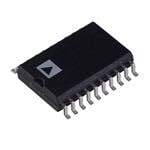
| 供应商器件封装 | 20-QSOP |
| 信噪比 | 94 dB |
| 分辨率 | 16 bit |
| 包装 | 管件 |
| 商标 | Analog Devices |
| 安装类型 | 表面贴装 |
| 安装风格 | SMD/SMT |
| 封装 | Tube |
| 封装/外壳 | 20-SSOP(0.154",3.90mm 宽) |
| 封装/箱体 | QSOP-20 |
| 工作温度 | -40°C ~ 125°C |
| 工作电源电压 | 2.5 V |
| 工厂包装数量 | 56 |
| 接口类型 | SPI |
| 数据接口 | SPI |
| 最大功率耗散 | 12 mW |
| 最大工作温度 | + 125 C |
| 最小工作温度 | - 40 C |
| 标准包装 | 1 |
| 特性 | 同步采样 |
| 特色产品 | http://www.digikey.cn/product-highlights/zh/analog-devices-ad7903-analogtodigital-converter/52097http://www.digikey.cn/product-highlights/cn/zh/analog-devices-select-q2-2014-products/4186 |
| 电压参考 | 2.4 V to 5.1 V |
| 电压源 | 单电源 |
| 结构 | SAR |
| 转换器数 | 2 |
| 转换速率 | 1 MS/s |
| 输入数和类型 | 2 个差分 |
| 输入类型 | Differential |
| 通道数量 | 2 Channel |
| 配用 | /product-detail/zh/EVAL-AD7903SDZ/EVAL-AD7903SDZ-ND/4725477 |
| 采样率(每秒) | 1M |


- 商务部:美国ITC正式对集成电路等产品启动337调查
- 曝三星4nm工艺存在良率问题 高通将骁龙8 Gen1或转产台积电
- 太阳诱电将投资9.5亿元在常州建新厂生产MLCC 预计2023年完工
- 英特尔发布欧洲新工厂建设计划 深化IDM 2.0 战略
- 台积电先进制程称霸业界 有大客户加持明年业绩稳了
- 达到5530亿美元!SIA预计今年全球半导体销售额将创下新高
- 英特尔拟将自动驾驶子公司Mobileye上市 估值或超500亿美元
- 三星加码芯片和SET,合并消费电子和移动部门,撤换高东真等 CEO
- 三星电子宣布重大人事变动 还合并消费电子和移动部门
- 海关总署:前11个月进口集成电路产品价值2.52万亿元 增长14.8%


PDF Datasheet 数据手册内容提取
Dual Differential 16-Bit, 1 MSPS PulSAR ADC 12.0 mW in QSOP Data Sheet AD7903 FEATURES GENERAL DESCRIPTION 16-bit resolution with no missing codes The AD7903 is a dual 16-bit, successive approximation, analog- Throughput: 1 MSPS to-digital converter (ADC) that operates from a single power Low power dissipation supply, VDDx, per ADC. It contains two low power, high speed, 7.0 mW at 1 MSPS (VDD1 and VDD2 only) 16-bit sampling ADCs and a versatile serial port interface (SPI). 12.0 mW at 1 MSPS (total) On the CNVx rising edge, the AD7903 samples the voltage 140 µW at 10 kSPS difference between the INx+ and INx− pins. The voltages on INL: ±0.5 LSB typical, ±2.0 LSB maximum these pins usually swing in opposite phases between 0 V and SINAD: 93.5 dB at 1 kHz V . The externally applied reference voltage of the REFx pins REF THD: −112 dB at 1 kHz (V ) can be set independently from the supply voltage pins, REF True differential analog input range: ±VREF VDDx. The power of the device scales linearly with throughput. 0 V to V with V between 2.4 V to 5.1 V REF REF Using the SDIx inputs, the SPI-compatible serial interface can Allows use of any input range also daisy-chain multiple ADCs on a single 3-wire bus and provide Easy to drive with the ADA4941-1 an optional busy indicator. It is compatible with 1.8 V, 2.5 V, 3 V, No pipeline delay or 5 V logic, using the separate VIOx supplies. Single-supply 2.5 V operation with 1.8 V/2.5 V/3 V/5 V logic interface The AD7903 is available in a 20-lead QSOP package with operation Serial port interface (SPI)/QSPI/MICROWIRE/DSP compatible specified from −40°C to +125°C. 20-lead QSOP package Table 1. MSOP 14-/16-/18-Bit PulSAR® ADCs Wide operating temperature range: −40°C to +125°C 100 250 400 kSPS 1000 ADC Bits kSPS kSPS to 500 kSPS kSPS Driver APPLICATIONS 18 AD76911 AD76901 AD79821 ADA4941-1 Battery-powered equipment ADA4841-x Communications 16 AD7680 AD76851 AD76861 AD79801 ADA4941-1 Automated test equipment (ATE) AD7683 AD76871 AD76881 AD7903 ADA4841-x Data acquisition AD7684 AD7694 AD76931 AD7902 Medical instrumentation 14 AD7940 AD79421 AD79461 Redundant measurement 1 Pin-for-pin compatible. Simultaneous sampling FUNCTIONAL BLOCK DIAGRAM REF = 2.5V TO 5V 2.5V REF1 REF2 VDD1 VDD2 ADA4941-1 VIO1 VIO1/VIO2 REF IN1+ SDI1 SDI1/SDI2 ADC1 SCK1 SCK1/SCK2 CNV1 CNV1/CNV2 ±10V, ±5V, ... IN1– SDO1 SDO1 ADA4941-1 VIO2 REF IN2+ 3-WIRE OR 4-WIRE SDI2 INTERFACE ADC2 SCK2 (SPI, CS, AND CHAIN MODES) CNV2 ±10V, ±5V, ... IN2– SDO2 SDO2 GND AD7903 11755-001 Figure 1. Rev. B Document Feedback Information furnished by Analog Devices is believed to be accurate and reliable. However, no responsibility is assumed by Analog Devices for its use, nor for any infringements of patents or other One Technology Way, P.O. Box 9106, Norwood, MA 02062-9106, U.S.A. rights of third parties that may result from its use. Specifications subject to change without notice. No license is granted by implication or otherwise under any patent or patent rights of Analog Devices. Tel: 781.329.4700 ©2013–2014 Analog Devices, Inc. All rights reserved. Trademarks and registered trademarks are the property of their respective owners. Technical Support www.analog.com
AD7903 Data Sheet TABLE OF CONTENTS Features .............................................................................................. 1 Analog Inputs.............................................................................. 15 Applications ....................................................................................... 1 Driver Amplifier Choice ........................................................... 16 General Description ......................................................................... 1 Single-to-Differential Driver .................................................... 16 Functional Block Diagram .............................................................. 1 Voltage Reference Input ............................................................ 17 Revision History ............................................................................... 2 Power Supply ............................................................................... 17 Specifications ..................................................................................... 3 Digital Interface .......................................................................... 17 Timing Specifications .................................................................. 5 CS Mode ...................................................................................... 18 Absolute Maximum Ratings ............................................................ 6 Chain Mode ................................................................................ 22 ESD Caution .................................................................................. 6 Applications Information .............................................................. 24 Pin Configuration and Function Descriptions ............................. 7 Simultaneous Sampling ............................................................. 24 Typical Performance Characteristics ............................................. 8 Functional Safety Considerations ............................................ 25 Terminology .................................................................................... 13 Layout ............................................................................................... 26 Theory of Operation ...................................................................... 14 Evaluating Performance of the AD7903.................................. 26 Circuit Information .................................................................... 14 Outline Dimensions ....................................................................... 27 Converter Operation .................................................................. 14 Ordering Guide .......................................................................... 27 Typical Connection Diagram.................................................... 15 REVISION HISTORY 8/14—Rev. A to Rev. B Changed Standby Current Unit from nA to µA ........................... 4 Changes to Power Supply Section ................................................ 17 1/14—Rev. 0 to Rev. A Change to Gain Error Temperature Drift Parameter .................. 3 Changes to Figure 12 ........................................................................ 9 Changes to Figure 17 and Figure 20............................................. 10 Changes to Figure 28 ...................................................................... 11 12/13—Revision 0: Initial Version Rev. B | Page 2 of 28
Data Sheet AD7903 SPECIFICATIONS V = 2.5 V, V = 2.3 V to 5.5 V, V = 5 V, T = −40°C to +125°C, unless otherwise noted.1 DD IO REF A Table 2. Parameter Test Conditions/Comments Min Typ Max Unit RESOLUTION 16 Bits ANALOG INPUT Voltage Range INx+ − INx− −V +V V REF REF Absolute Input Voltage INx+, INx− −0.1 V + 0.1 V REF Common-Mode Input Range INx+, INx− V × 0.475 V × 0.5 V × 0.525 V REF REF REF Analog Input CMRR f = 450 kHz 67 dB IN Leakage Current at 25°C Acquisition phase 200 nA Input Impedance See the Analog Inputs section ACCURACY No Missing Codes 16 Bits Differential Nonlinearity Error V = 5 V −1.0 ±0.4 +1.0 LSB2 REF V = 2.5 V ±0.7 LSB2 REF Integral Nonlinearity Error V = 5 V −2.0 ±0.5 +2.0 LSB2 REF V = 2.5 V ±0.4 LSB2 REF Transition Noise V = 5 V 0.75 LSB2 REF V = 2.5 V 1.2 LSB2 REF Gain Error3 T to T −0.04 ±0.006 +0.04 % FS MIN MAX Gain Error Temperature Drift 0.19 ppm/°C Gain Error Match3 T to T 0.0 0.025 % FS MIN MAX Offset Error3 T to T −0.5 ±0.015 +0.5 mV MIN MAX Offset Temperature Drift 0.3 ppm/°C Offset Error Match3 T to T 0.05 1.0 mV MIN MAX Power Supply Sensitivity V = 2.5 V ± 5% ±0.1 LSB2 DD THROUGHPUT Conversion Rate V ≥ 2.3 V up to 85°C, V ≥ 3.3 V 0 1 MSPS IO IO above 85°C, up to 125°C Transient Response Full-scale step 290 ns AC ACCURACY Dynamic Range V = 5 V 95.5 dB4 REF V = 2.5 V 92.5 dB4 REF Oversampled Dynamic Range f = 10 kSPS 113.5 dB4 OUT Signal-to-Noise Ratio (SNR) f = 1 kHz, V = 5 V 92 94 dB4 IN REF f = 1 kHz, V = 2.5 V 89 91 dB4 IN REF Spurious-Free Dynamic Range (SFDR) f = 1 kHz −115 dB4 IN Total Harmonic Distortion (THD) f = 1 kHz −112 dB4 IN Signal-to-(Noise + Distortion) (SINAD) f = 1 kHz, V = 5 V 91.5 93.5 dB4 IN REF f = 1 kHz, V = 2.5 V 88.5 90.5 dB4 IN REF Channel-to-Channel Isolation f = 10 kHz −120 dB4 IN 1 In this data sheet, the voltages for the VDDx, VIOx, and REFx pins are indicated by VDD, VIO, and VREF, respectively. 2 With the 5 V input range, 1 LSB = 152.6 µV. With the 2.5 V input range, 1 LSB = 76.3 µV. 3 See the Terminology section. These specifications include full temperature range variation, but they do not include the error contribution from the external reference. 4 All specifications in decibels (dB) are referred to a full-scale input FSR. Although these parameters are referred to full scale, they are tested with an input signal at 0.5 dB below full scale, unless otherwise specified. Rev. B | Page 3 of 28
AD7903 Data Sheet V = 2.5 V, V = 2.3 V to 5.5 V, T = −40°C to +125°C, unless otherwise noted.1 DD IO A Table 3. Parameter Test Conditions/Comments Min Typ Max Unit REFERENCE Voltage Range 2.4 5.1 V Load Current 1 MSPS, V = 5 V, each ADC 330 µA REF SAMPLING DYNAMICS −3 dB Input Bandwidth 10 MHz Aperture Delay V = 2.5 V 2.0 ns DD Aperture Delay Match V = 2.5 V 2.0 ns DD DIGITAL INPUTS Logic Levels V V > 3 V −0.3 +0.3 × V V IL IO IO V ≤ 3 V −0.3 +0.1 × V V IO VIO V V > 3 V 0.7 × V V + 0.3 V IH IO IO IO V ≤ 3 V 0.9 × V V + 0.3 V IO IO IO I −1 +1 µA IL I −1 +1 µA IH DIGITAL OUTPUTS Data Format Twos complement Bits Pipeline Delay No delay; conversion results available 0 Samples immediately after conversion is complete V I = +500 µA 0.4 V OL SINK V I = −500 µA V − 0.3 V OH SOURCE IO POWER SUPPLIES VDDx 2.375 2.5 2.625 V VIOx Specified performance 2.3 5.5 V VIOx Range Full Range 1.8 5.5 V I Each ADC 1.4 1.6 mA VDDx I Each ADC 0.2 0.45 mA VIOx Standby Current2, 3 V and V = 2.5 V, 25°C 0.35 µA DD IO Power Dissipation 10 kSPS throughput 140 µW 1 MSPS throughput 12.0 16 mW VDD Only 7.0 mW REF Only 3.3 mW VIO Only 1.7 mW Energy per Conversion 7.0 nJ/sample TEMPERATURE RANGE4 Specified Performance T to T −40 +125 °C MIN MAX 1 In this data sheet, the voltages for the VDDx, VIOx, and REFx pins are indicated by VDD, VIO, and VREF, respectively. 2 With all digital inputs forced to VIOx or to ground as required. 3 During the acquisition phase. 4 Contact Analog Devices, Inc., for the extended temperature range. Rev. B | Page 4 of 28
Data Sheet AD7903 TIMING SPECIFICATIONS −40°C to +125°C, V = 2.37 V to 2.63 V, V = 2.3 V to 5.5 V, unless otherwise stated. See Figure 2 and Figure 3 for load conditions. DD IO Table 4. Parameter Symbol Min Typ Max Unit Conversion Time (CNVx Rising Edge to Data Available) t 500 710 ns CONV Acquisition Time t 290 ns ACQ Time Between Conversions t CYC VIOx Above 2.3 V 1000 ns CNVx Pulse Width (CS Mode) t 10 ns CNVH SCKx Period (CS Mode) t SCK VIOx Above 4.5 V 10.5 ns VIOx Above 3 V 12 ns VIOx Above 2.7 V 13 ns VIOx Above 2.3 V 15 ns SCKx Period (Chain mode) t SCK VIOx Above 4.5 V 11.5 ns VIOx Above 3 V 13 ns VIOx Above 2.7 V 14 ns VIOx Above 2.3 V 16 ns SCKx Low Time t 4.5 ns SCKL SCKx High Time t 4.5 ns SCKH SCKx Falling Edge to Data Remains Valid t 3 ns HSDO SCKx Falling Edge to Data Valid Delay t DSDO VIOx Above 4.5 V 9.5 ns VIOx Above 3 V 11 ns VIOx Above 2.7 V 12 ns VIOx Above 2.3 V 14 ns CNVx or SDIx Low to SDOx, D15 (MSB) Valid (CS Mode) t EN VIOx Above 3 V 10 ns VIOx Above 2.3 V 15 ns CNVx or SDIx High or Last SCKx Falling Edge to SDOx High Impedance (CS Mode) t 20 ns DIS SDIx Valid Setup Time from CNVx Rising Edge (CS Mode) t 5 ns SSDICNV SDIx Valid Hold Time from CNVx Rising Edge (CS Mode) t 2 ns HSDICNV SCKx Valid Setup Time from CNVx Rising Edge (Chain Mode) t 5 ns SSCKCNV SCKx Valid Hold Time from CNVx Rising Edge (Chain Mode) t 5 ns HSCKCNV SDIx Valid Setup Time from SCKx Falling Edge (Chain Mode) t 2 ns SSDISCK SDIx Valid Hold Time from SCKx Falling Edge (Chain Mode) t 3 ns HSDISCK SDIx High to SDOx High (Chain Mode with Busy Indicator) t 15 ns DSDOSDI Y% VIOx1 500µA IOL X% VIOx1 t t DELAY DELAY TO SDOx 1.4V VIH2 VIH2 CL VIL2 VIL2 20pF 500µA IOH 11755-002 12IFMNOIPNRUIM TVUSIOM Px A V≤RI H3A .A0MVNE,D TX EM =RA 9XIN0I M ATUNAMDB LYVE I=L 3 U1.0S;E FDO. RS EVEIO SxP >E C3.I0FVIC, AX T=I O70N SA NFDO RY D= I3G0I.TAL 11755-003 Figure 2. Load Circuit for Digital Interface Timing Figure 3. Voltage Levels for Timing Rev. B | Page 5 of 28
AD7903 Data Sheet ABSOLUTE MAXIMUM RATINGS Table 5. Stresses above those listed under Absolute Maximum Ratings Parameter Rating may cause permanent damage to the device. This is a stress Analog Inputs rating only; functional operation of the device at these or any INx+, INx− to GND1 −0.3 V to V + 0.3 V or ±10 mA other conditions above those indicated in the operational REF Supply Voltage section of this specification is not implied. Exposure to absolute REFx, VIOx to GND −0.3 V to +6.0 V maximum rating conditions for extended periods may affect VDDx to GND −0.3 V to +3.0 V device reliability. VDDx to VIOx +3 V to −6 V ESD CAUTION Digital Inputs to GND −0.3 V to V + 0.3 V IO Digital Outputs to GND −0.3 V to V + 0.3 V IO Storage Temperature Range −65°C to +150°C Junction Temperature 150°C Lead Temperatures Vapor Phase (60 sec) 255°C Infrared (15 sec) 260°C 1 See the Analog Inputs section for an explanation of INx+ and INx−. Rev. B | Page 6 of 28
Data Sheet AD7903 PIN CONFIGURATION AND FUNCTION DESCRIPTIONS REF1 1 20 VIO1 VDD1 2 19 SDI1 IN1+ 3 18 SCK1 AD7903 IN1– 4 17 SDO1 TOP VIEW GND 5 (Not to Scale) 16 CNV1 REF2 6 15 VIO2 VDD2 7 14 SDI2 IN2+ 8 13 SCK2 IN2– 9 12 SDO2 GND 10 11 CNV2 11755-004 Figure 4. Pin Configuration Table 6. Pin Function Descriptions Pin No. Mnemonic Type1 Description 1, 6 REF1, REF2 AI Reference Input Voltage. The REFx range is 2.4 V to 5.1 V. These pins are referred to the GND pin, and decouple each pin closely to the GND pin with a 10 μF capacitor. 2, 7 VDD1, VDD2 P Power Supplies. 3, 8 IN1+, IN2+ AI Differential Positive Analog Inputs. 4, 9 IN1−, IN2− AI Differential Negative Analog Inputs. 5, 10 GND P Power Supply Ground. 11, 16 CNV2, CNV1 DI Conversion Inputs. These inputs have multiple functions. On the leading edge, they initiate conversions and select the interface mode of the device: chain mode or active low chip select (CS) mode. In CS mode, the SDOx pins are enabled when the CNVx pins are low. In chain mode, the data must be read when the CNVx pins are high. 12, 17 SDO2, SDO1 DO Serial Data Outputs. The conversion result is output on these pins. The conversion result is synchronized to SCKx. 13, 18 SCK2, SCK1 DI Serial Data Clock Inputs. When the device is selected, the conversion results are shifted out by these clocks. 14, 19 SDI2, SDI1 DI Serial Data Inputs. These inputs provide multiple functions. They select the interface mode of the ADC, as follows: CS mode is selected if the SDIx pins are high during the CNVx rising edge. In this mode, either SDIx or CNVx can enable the serial output signals when low. If SDIx or CNVx is low when the conversion is complete, the busy indicator feature is enabled. 15, 20 VIO2, VIO1 P Input/Output Interface Digital Power. Nominally at the same supply as the host interface (2.5 V or 3.3 V). 1 AI = analog input, DI = digital input, DO = digital output, and P = power. Rev. B | Page 7 of 28
AD7903 Data Sheet TYPICAL PERFORMANCE CHARACTERISTICS V = 2.5 V, V = 5.0 V, V = 3.3 V, T = 25°C, f = 1 MSPS, unless otherwise noted. DD REF IO A SAMPLE 1.0 1.0 POSITIVE INL:+0.35LSB POSITIVEDNL:+0.31LSB NEGATIVE INL:–0.39LSB NEGATIVEDNL:–0.38LSB 0.8 0.8 0.6 0.6 0.4 0.4 B) 0.2 )B 0.2 NL(LS 0 NL(LS 0 I –0.2 D –0.2 –0.4 –0.4 –0.6 –0.6 –0.8 –0.8 –1.00 16384 C3O27D6E8 49152 65536 11755-405 –1.00 16384 C3O27D6E8 49152 65536 40811755- Figure 5. Integral Nonlinearity vs. Code, VREF = 5 V Figure 8. Differential Nonlinearity vs. Code, VREF = 5 V 1.0 1.0 POSITIVE INL:+0.39LSB POSITIVEDNL:+0.39LSB 0.8 NEGATIVE INL:–0.44LSB 0.8 NEGATIVEDNL:–0.39LSB 0.6 0.6 0.4 0.4 B) 0.2 B) 0.2 NL(LS 0 NL(LS 0 I –0.2 D –0.2 –0.4 –0.4 –0.6 –0.6 –0.8 –0.8 –1.00 16384 C3O27D6E8 49152 65536 11755-406 –1.00 16384 C3O27D6E8 49152 65536 11755-409 Figure 6. Integral Nonlinearity vs. Code, VREF = 2.5 V Figure 9. Differential Nonlinearity vs. Code, VREF = 2.5 V 0 0 fSAMPLE = 1MSPS fSAMPLE = 1MSPS –20 fIN = 10kHz –20 fIN = 10kHz SNR = 95.04dB SNR = 91.96dB THD = –117.3dB THD = –110.2dB –40 SFDR = 114.6dB –40 SFDR = 114.5dB SINAD = 95.02dB SINAD = 91.91dB –60 –60 dB) –80 dB) –80 R ( R ( SN –100 SN –100 –120 –120 –140 –140 –160 –160 –180 –180 0 100 F2R0E0QUENCY (3k0H0z) 400 500 11755-407 0 100 F2R0E0QUENCY (3k0H0z) 400 500 11755-410 Figure 7. FFT Plot, VREF = 5 V Figure 10. FFT Plot, VREF = 2.5 V Rev. B | Page 8 of 28
Data Sheet AD7903 45000 45000 40000 40000 S35000 S35000 E E C C N N E30000 E30000 R R R R U U C25000 C25000 C C O O F 20000 F 20000 O O R R BE15000 BE15000 M M U U N10000 N10000 5000 5000 0 FFE1 FFE2 FFE3 FFE4CFOFDEE5S FINF EH6EXFFE7 FFE8 FFE9FFEA 11755-411 0 FFF1FFF2FFF3FFF4FCFOF5DEFSF FIN6 FHFEFX7FFF8FFF9FFFAFFFB 11755-414 Figure 11. Histogram of a DC Input at the Code Center, VREF = 5 V Figure 14. Histogram of a DC Input at the Code Center, VREF = 2.5 V 40000 98 35000 97 S E30000 C N E 96 RR25000 OCCU20000 R (dB) 95 F N O S R 15000 BE 94 M U10000 N 93 5000 0 FFD2FFD3FFD4FFD5COFFDDE6S FINF DH7EXFFD8FFD9FFDAFFDB 11755-412 92–10 –9 –8 –7 IN–P6UT L–E5VEL –(4dB) –3 –2 –1 0 11755-415 Figure 12. Histogram of a DC Input at the Code Transition, VREF = 5 V Figure 15. SNR vs. Input Level 100 16.0 –95 115 SNR 98 SINAD ENOB 15.5 –100 110 96 15.0 SFDR 94 NR, SINAD (dB) 998208 111344...505 ENOB (Bits) THD (dB)––111005 110005 SFDR (dB) S –115 95 86 THD 13.0 84 –120 90 12.5 82 80 2.252.502.753.00RE3.F2E5R3E.5N0C3E. 7V5O4L.T00AG4.E2 5(V4).504.755.005.25 12.0 11755-413 –1252.25 2.75 R3E.2F5ERENCE3. 7V5OLTAG4E. 2(5V) 4.75 5.2855 11755-416 Figure 13. SNR, SINAD, and ENOB vs. Reference Voltage Figure 16. THD, SFDR vs. Reference Voltage Rev. B | Page 9 of 28
AD7903 Data Sheet 96 –80 95 –85 94 –90 93 92 –95 AD (dB) 91 D (dB)–100 N 90 H SI T 89 –105 88 –110 87 –115 86 85 –120 10 INPUT FREQUENCY (k1H0z0) 11755-417 10 INPUT FREQUENCY (k1H0z0) 11755-420 Figure 17. SINAD vs. Input Frequency Figure 20. THD vs. Input Frequency 94.8 –100 94.6 –105 94.4 B)94.2 B)–110 d d R ( D ( N H S94.0 T –115 93.8 –120 93.6 93.4 –125 –55 –35 –15 5TEMP2E5RATU4R5E (°C6)5 85 105 125 11755-418 –55 –35 –15 5TEMP2E5RATU4R5E (°C6)5 85 105 125 11755-421 Figure 18. SNR vs. Temperature Figure 21. THD vs. Temperature 1.4 1.6 IVDD TA = 25°C 1.4 1.2 1.2 1.0 A) A) 1.0 m m ENT ( 0.8 ENT ( 0.8 RR 0.6 RR IVDD CU IREF CU 0.6 0.4 0.4 IVIO 0.2 0.2 IVIO 20.375 2.425 V2D.4D75 VOLTAG2E.5 (2V5) 2.575 2.625 11755-050 010 SAMPLE R10A0TE (kSPS) 1000 11755-422 Figure 19. Operating Currents of Each ADC vs. VDD Supply Voltage Figure 22. Operating Currents of Each ADC vs. Sample RateCr Rev. B | Page 10 of 28
Data Sheet AD7903 1.4 8 IVDD 1.2 7 6 1.0 A) A) 5 RENT (m 0.8 RENT (µ 4 R 0.6 R CU IREF CU 3 IVDD + IVIO 0.4 2 IVIO 0.2 1 0–55 –35 –15 5TEMP2E5RATU4R5E (°C6)5 85 105 125 11755-053 0–55 –35 –15 5TEMP2E5RATU4R5E (°C6)5 85 105 125 11755-054 Figure 23. Operating Currents of Each ADC vs. Temperature Figure 26. Power-Down Current of Each ADC vs. Temperature 0.10 0.10 0.08 0.08 0.06 V) 0.06 m mV) 0.04 CH ( 0.04 R ( 0.02 AT 0.02 O M ERR 0 OR 0 FSET –0.02 T ERR–0.02 F E O–0.04 S–0.04 F F O –0.06 –0.06 –0.08 –0.08 –0.10 –0.10 –55 –35 –15 5TEMP2E5RATU4R5E (°C6)5 85 105 125 11755-424 –55 –35 –15 5TEMP2E5RATU4R5E (°C6)5 85 105 125 11755-427 Figure 24. Offset Error vs. Temperature Figure 27. Offset Error Match vs. Temperature 0.05 0.010 0.03 FS) 0.005 % FS) 0.01 CH (% R ( AT N ERRO–0.01 RROR M 0 AI E G N GAI–0.005 –0.03 –0.05–55 –35 –15 5TEMP2E5RATU4R5E (°C6)5 85 105 125 11755-425 –0.010–55 –35 –15 5TEMP2E5RATU4R5E (°C6)5 85 105 125 11755-428 Figure 25. Gain Error vs. Temperature Figure 28. Gain Error Match vs. Temperature Rev. B | Page 11 of 28
AD7903 Data Sheet –112 –112 fIN=10kHz B) –113 fSAMPLE=1MSPS dB) (d N (–114 N –114 O TIO ATI LA –115 OL–116 O S L IS –116 EL I NE NN–118 AN –117 HA H C O-C –118 TO-–120 L-T EL- E –119 N N N N A–122 A H H –120 C C –121 –124 –55 –35 –15 5TEMP2E5RATU4R5E(°C6)5 85 105 125 11755-429 10 INPUT FREQUENCY (M1H0z0) 11755-430 Figure 29. Channel-to-Channel Isolation vs. Temperature Figure 30. Channel-to-Channel Isolation vs. Input Frequency Rev. B | Page 12 of 28
Data Sheet AD7903 TERMINOLOGY Spurious-Free Dynamic Range (SFDR) Integral Nonlinearity Error (INL) SFDR is the difference, in decibels (dB), between the rms INL refers to the deviation of each individual code from a line amplitude of the input signal and the peak spurious signal. drawn from negative full scale through positive full scale. The point used as negative full scale occurs ½ LSB before the first Effective Number of Bits (ENOB) code transition. Positive full scale is defined as a level 1½ LSB ENOB is a measurement of the resolution with a sine wave beyond the last code transition. The deviation is measured from input. It is related to SINAD by the following formula: the middle of each code to the true straight. ENOB = (SINAD − 1.76)/6.02 dB Differential Nonlinearity Error (DNL) ENOB is expressed in bits. In an ideal ADC, code transitions are 1 LSB apart. DNL is the Noise Free Code Resolution maximum deviation from this ideal value. It is often specified in Noise free code resolution is the number of bits beyond which it terms of resolution for which no missing codes are guaranteed. is impossible to distinctly resolve individual codes. It is calculated Offset Error as follows: Offset error is the difference between the ideal midscale voltage Noise Free Code Resolution = log(2N/Peak-to-Peak Noise) (that is, 0 V) and the actual voltage producing the midscale 2 output code (that is, 0 LSB). Noise free code resolution is expressed in bits. Offset Error Match Effective Resolution Effective resolution is calculated as follows: It is the difference in offsets, expressed in millivolts between the channels of a multichannel converter. It is computed with the Effective Resolution = log2(2N/RMS Input Noise) following equation: Effective resolution is expressed in bits. Offset Matching = VOFFSET − VOFFSET MAX MIN Total Harmonic Distortion (THD) where: THD is the ratio of the rms sum of the first five harmonic VOFFSET is the most positive offset error. components to the rms value of a full-scale input signal and is MAX VOFFSET is the most negative offset error. expressed in decibels (dB). MIN Offset matching is usually expressed in millivolts with the full- Dynamic Range scale input range stated in the product data sheet. Dynamic range is the ratio of the rms value of the full scale to the total rms noise measured with the inputs shorted together. Gain Error The value for dynamic range is expressed in decibels (dB). It is The first transition (from 100 … 00 to 100 … 01) should occur measured with a signal at −60 dBFS to include all noise sources at a level ½ LSB above nominal negative full scale (−4.999981 V and DNL artifacts. for the ±5 V range). The last transition (from 011 … 10 to 011 … 11) occurs for an analog voltage that is 1½ LSB below the Signal-to-Noise Ratio (SNR) nominal full scale (4.999943 V for the ±5 V range). The gain SNR is the ratio of the rms value of the actual input signal to the error is the deviation of the difference between the actual level rms sum of all other spectral components below the Nyquist of the last transition and the actual level of the first transition from frequency, excluding harmonics and dc. The value for SNR is the difference between the ideal levels. expressed in decibels (dB). Gain Error Match Signal-to-(Noise + Distortion) (SINAD) Ratio SINAD is the ratio of the rms value of the actual input signal to It is the ratio of the maximum full scale to the minimum full the rms sum of all other spectral components below the Nyquist scale of a multichannel ADC. It is expressed as a percentage of frequency, including harmonics but excluding dc. The value for full scale using the following equation: SINAD is expressed in decibels (dB). FSR −FSR Aperture Delay GainMatching = FSRMMAAXX+FSRMMIINN ×100% Ais ptheret utirme ed ebleatyw iese tnh eth me eraissiunrge eodf gteh eo fa tchqeu iCsiNtiVonx pineprfuotr amnadn ce. It 2 when the input signal is held for a conversion. where: Transient Response FSR is the most positive gain error of the ADC. MAX Transient response is the time required for the ADC to accurately FSR is the most negative gain error. MIN acquire its input after a full-scale step function is applied. Rev. B | Page 13 of 28
AD7903 Data Sheet THEORY OF OPERATION INx+ MSB SWITCHESCONTROL LSB SWx+ 32,768C 16,384C 4C 2C C C BUSY REFx COMP CONTROL LOGIC GND OUTPUTCODE 32,768C 16,384C 4C 2C C C LSB SWx– MSB CNVx INx– 11755-011 Figure 31. ADC Simplified Schematic CIRCUIT INFORMATION the comparator input varies by binary-weighted voltage steps (V /2, V /4 ... V /65,536). The control logic toggles these REF REF REF The AD7903 is a fast, low power, precise, dual 16-bit ADC switches, starting with the MSB, to bring the comparator back using a successive approximation architecture. into a balanced condition. After the completion of this process, The AD7903 is capable of simultaneously converting 1,000,000 the part returns to the acquisition phase, and the control logic samples per second (1 MSPS) and powers down between con- generates the ADC output code and a busy signal indicator. versions. When operating at 10 kSPS, for example, it typically Because the AD7903 has an on-board conversion clock, the consumes 70 μW per ADC, making it ideal for battery-powered serial clock, SCKx, is not required for the conversion process. applications. Transfer Functions The AD7903 provides the user with an on-chip track-and-hold The ideal transfer characteristic for the AD7903 is shown in and does not exhibit any pipeline delay or latency, making it Figure 32 and Table 7. ideal for multichannel multiplexed applications. The AD7903 can be interfaced to any 1.8 V to 5 V digital logic T) N family. It is available in a 20-lead QSOP that allows flexible ME 011...111 configurations. LE 011...110 MP 011...101 The device is pin-for-pin compatible with the pseudo differential, CO S 16-bit AD7902. O W T CONVERTER OPERATION E ( D O The AD7903 is a dual successive approximation ADC based on C C D a charge redistribution DAC. Figure 31 shows the simplified A 100...010 schematic of the ADC. The capacitive DAC consists of two 100...001 identical arrays of 16 binary-weighted capacitors, which are 100...000 –FSR –FSR + 1 LSB +FSR – 1 LSB cDounrninecgt tehde t aoc tqhuei stiwtioo nco pmhapsaer aotfo era icnhp uAtDs. C, terminals of the –FSR + 0.5 LSB ANALOG IN+PFUSRT – 1.5 LSB 11755-112 Figure 32. ADC Ideal Transfer Function array tied to the input of the comparator are connected to GND via SWx+ and SWx−. All independent switches are connected Table 7. Output Codes and Ideal Input Voltages to the analog inputs. Therefore, the capacitor arrays are used as Analog Input, Digital Output sampling capacitors and acquire the analog signal on the INx+ Description VREF = 5 V Code (Hex) and INx− inputs. When the acquisition phase is complete and FSR − 1 LSB +4.999962 V 0x7FFF1 the CNVx input goes high, a conversion phase is initiated. When Midscale + 1 LSB +38.15 μV 0x0001 the conversion phase begins, SWx+ and SWx− are opened first. Midscale 0 V 0x0000 The two capacitor arrays are then disconnected from the inputs Midscale − 1 LSB −38.15 μV 0xFFFF and connected to the GND input. Therefore, the differential −FSR + 1 LSB −4.999962 V 0x8001 voltage between the INx+ and INx− inputs, captured at the end −FSR −5 V 0x80002 of the acquisition phase, is applied to the comparator inputs, causing the comparator to become unbalanced. By switching 1 This is also the code for an overranged analog input (VIN+ − VIN− above VREF − VGND). 2 This is also the code for an underranged analog input (VIN+ − VIN− below VGND). each element of the capacitor array between GND and REFx, Rev. B | Page 14 of 28
Data Sheet AD7903 TYPICAL CONNECTION DIAGRAM 90 Figure 35 shows an example of the recommended connection 85 diagram for the AD7903 when multiple supplies are available. ANALOG INPUTS 80 B) Figure 33 shows an equivalent circuit of the input structure of d R (75 the AD7903. R M C The two diodes, D1 and D2, provide ESD protection for the 70 analog inputs, INx+ and INx−. The analog input signal must never exceed the reference input voltage (VREF) by more than 0.3 V. If 65 the analog input signal exceeds this level, the diodes become fhoarnwdalerd a bfoiarswedar adn-bdi satsaerdt ccuonrrdeunct toinf g1 3c0u rmreAn tm. Tahxeimseu dmio. des can 601k 10k FREQU1E00NkCY (Hz) 1M 10M 11755-040 However, if the supplies of the input buffer (for example, the Figure 34. Analog Input CMRR vs. Frequency supplies of the ADA4841-1 in Figure 35) are different from During the acquisition phase, the impedance of the analog inputs those of the V , the analog input signal may eventually exceed REF (INx+ or INx−) can be modeled as a parallel combination of the the supply rails by more than 0.3 V. In such a case (for example, C capacitor and the network formed by the series connection PIN an input buffer with a short circuit), the current limitation can of R and C . C is primarily the pin capacitance. R is typically IN IN PIN IN be used to protect the device. 400 Ω and is a lumped component composed of serial resistors REFx and the on resistance of the switches. C is typically 30 pF and IN is mainly the ADC sampling capacitor. D1 RIN CIN INx+ OR INx– During the sampling phase, where the switches are closed, the CPIN D2 input impedance is limited to C . R and C make a one-pole, GND 11755-114 lnoowis-ep.a ss filter that reduces undesPIiNrablIeN aliasingIN effects and limits Figure 33. Equivalent Analog Input Circuit When the source impedance of the driving circuit is low, the The analog input structure allows for the sampling of the AD7903 can be driven directly. Large source impedances differential signal between INx+ and INx−. By using these significantly affect the ac performance, especially THD. The differential inputs, signals common to both inputs, and within dc performances are less sensitive to the input impedance. The the allowable common-mode input range, are rejected. maximum source impedance depends on the amount of THD that can be tolerated. The THD degrades as a function of the source impedance and the maximum input frequency. V+ REF1 2.5V 10µF2 100nF V+ 1.8VTO5V 100nF 20Ω 0VTOVREF 2.7nF REFx VDDx VIOx SDIx INx+ V– 4 SCKx AD7903 ADCx SDOx 3-WIRE INTERFACE V+ INx– CNVx GND 20Ω VREFTO0V 2.7nF ADA4841-13 V– 4 1SEETHEVOLTAGEREFERENCE INPUTSECTIONFORREFERENCESELECTION. 2CREF ISUSUALLYA10µFCERAMICCAPACITOR(X5R). 34SSOEEPEETITROHENECAODLMRFIMIVLEETNREDRAE.MDSPELLEAIFTYIHOEERUTAC NIHNAOFLICIOGEGUS RINEEPC5UT4IT.OSNS.ECTION. 11755-013 Figure 35. Typical Application Diagram with Multiple Supplies Rev. B | Page 15 of 28
AD7903 Data Sheet DRIVER AMPLIFIER CHOICE Table 8. Recommended Driver Amplifiers Although the AD7903 is easy to drive, the driver amplifier must Amplifier Typical Application meet the following requirements: ADA4941-1 Very low noise, low power, single to differential ADA4841-x Very low noise, small, and low power • The noise generated by the driver amplifier must be kept AD8021 Very low noise and high frequency as low as possible to preserve the SNR and transition noise AD8022 Low noise and high frequency performance of the AD7903. The noise from the driver is OP184 Low power, low noise, and low frequency filtered by the one-pole, low-pass filter of the AD7903 AD8655 5 V single supply, low noise analog input circuit, made by R and C or by the IN IN AD8605, AD8615 5 V single supply, low power external filter, if one is used. Because the typical noise of the AD7903 is 40 µV rms, the SNR degradation due to the SINGLE-TO-DIFFERENTIAL DRIVER amplifier is For applications using a single-ended analog signal, either bipolar or unipolar, the ADA4941-1 single-ended-to-differential driver 40 allows a differential input to the device. The schematic is shown SNR =20log LOSS π in Figure 36. 402+ f (Ne )2 2 −3dB N R1 and R2 set the attenuation ratio between the input range and the ADC range (V ). R1, R2, and C are chosen depending on where: REF F the desired input resistance, signal bandwidth, antialiasing, and f is the input bandwidth, in megahertz, of the AD7903 −3dB noise contribution. For example, for the ±10 V range with a 4 kΩ (10 MHz) or the cutoff frequency of the input filter, if one impedance, R1 = 4 kΩ and R2 = 1 kΩ. is used. N is the noise gain of the amplifier (for example, gain = 1 R3 and R4 set the common mode on the INx− input, and R5 and in buffer configuration; see Figure 35). R6 set the common mode on the INx+ input of the ADC. The eN is the equivalent input noise voltage of the op amp, in common mode must be close to VREF/2. For example, for the nV/√Hz. ±10 V range with a single supply, R3 = 8.45 kΩ, R4 = 11.8 kΩ, • For ac applications, the driver must have a THD performance R5 = 10.5 kΩ, and R6 = 9.76 kΩ. that is commensurate with the AD7903. • For multichannel, multiplexed applications, the driver amplifier and the AD7903 analog input circuit must settle for a full-scale step onto the capacitor array at a 16-bit level (0.0015%, 15 ppm). In the amplifier data sheet, settling at 0.1% to 0.01% is more commonly specified. This may differ significantly from the settling time at a 16-bit level. Be sure to verify the settling time prior to driver selection. R5 R6 R3 R4 +5V REF +5.2V 10µF +2.5V 100nF REF OUTN 20Ω REFx VDDx INx+ 2.7nF AD7903 OUTP 2.7nF ADCx 100nF INx– IN 20Ω GND FB ADA4941-1 ±10V, R1 –0.2V ±5V, .. R2 CF 11755-115 Figure 36. Single-Ended-to-Differential Driver Circuit Rev. B | Page 16 of 28
Data Sheet AD7903 VOLTAGE REFERENCE INPUT 10 The AD7903 voltage reference input, REF, has a dynamic input impedance and must therefore be driven by a low impedance mA) 1 source with efficient decoupling between the REFx and GND S ( T pins, as explained in the Layout section. EN IVDD R R When REF is driven by a very low impedance source (for CU 0.1 IREF G example, a reference buffer using the AD8031 or the AD8605), TIN IVIO a 10 µF (X5R, 0805 size) ceramic chip capacitor is appropriate RA E for optimum performance. OP 0.01 If an unbuffered reference voltage is used, the decoupling value depends on the reference used. For instance, a 22 µF (X5R, 1p2e0rf6o rsmizea)n cceer uamsinicg cah liopw c atepmacpiteorra tius raep dprriofpt rAiaDteR f4o3rx o rpetfiemreunmce . 0.00110000 SAMPLIN1G00 R00A0TE (SPS) 1000000 11755-137 Figure 38. Operating Currents per ADC vs. Sampling Rate If desired, a reference decoupling capacitor with values as small DIGITAL INTERFACE as 2.2 µF can be used with a minimal impact on performance, especially DNL. Although the AD7903 has a reduced number of pins, it offers flexibility in its serial interface modes. Regardless, there is no need for an additional lower value ceramic decoupling capacitor (for example, 100 nF) between the REFx When in CS mode, the AD7903 is compatible with SPI, QSPI, and GND pins. digital hosts, and DSPs. In this mode, the AD7903 can use either POWER SUPPLY a 3-wire or 4-wire interface. A 3-wire interface using the CNVx, SCKx, and SDOx signals minimizes wiring connections useful, The AD7903 uses two power supply pins per ADC: a core supply for instance, in isolated applications. A 4-wire interface using (VDDx) and a digital input/output interface supply (VIOx). the SDIx, CNVx, SCKx, and SDOx signals allows CNVx, which VIOx allows direct interface with any logic between 1.8 V and initiates the conversions, to be independent of the readback 5.5 V. To reduce the number of supplies needed, VIOx and VDDx timing (SDIx). This is useful in low jitter sampling or can be tied together. The AD7903 is independent of power supply simultaneous sampling applications. sequencing between VIOx and VDDx. Additionally, it is very When in chain mode, the AD7903 provides a daisy-chain feature insensitive to power supply variations over a wide frequency using the SDIx input for cascading multiple ADCs on a single range, as shown in Figure 37. data line similar to a shift register. With the AD7903 housing 95 two ADCs in one package, chain mode can be utilized to 90 acquire data from both ADCs while using only one set of 4-wire user interface signals. 85 The mode in which the device operates depends on the SDIx dB)80 level when the CNVx rising edge occurs. CS mode is selected if R ( SDIx is high, and chain mode is selected if SDIx is low. The R PS75 SDIx hold time is such that when SDIx and CNVx are connected together, chain mode is always selected. 70 In either mode, the AD7903 offers the option of forcing a start 65 bit in front of the data bits. This start bit can be used as a busy signal indicator to interrupt the digital host and trigger the data 601k 10kFREQUENCY (Hz1)00k 1M 11755-139 roeuatd tihneg .m Oatxhiemrwumise c, ownivtheorsuito an btiumsye ipnrdioicra ttoor r, ethade buascekr .m ust time Figure 37. PSRR vs. Frequency The busy indicator feature is enabled as follows: The AD7903 powers down automatically at the end of each conversion phase; therefore, the power scales linearly with the • In CS mode if CNVx or SDIx is low when the ADC sampling rate. This makes the part ideal for low sampling rates conversion ends (see Figure 42 and Figure 46). (of even a few hertz) and low battery-powered applications. • In chain mode if SCKx is high during the CNVx rising edge (see Figure 50). Rev. B | Page 17 of 28
AD7903 Data Sheet CS MODE However, to avoid generation of the busy signal indicator, CNVx must be returned high before the minimum conversion time CS Mode, 3-Wire Interface Without Busy Indicator elapses and then held high for the maximum possible conversion CS mode, using a 3-wire interface without a busy indicator, is time. When the conversion is complete, the AD7903 enters the usually used when a single AD7903 is connected to a SPI- acquisition phase and powers down. When CNVx goes low, the compatible digital host. MSB is automatically output onto SDOx. The remaining data bits The connection diagram is shown in Figure 39, and the are clocked by subsequent SCKx falling edges. The data is valid on corresponding timing diagram is shown in Figure 40. both SCKx edges. Although the rising edge can be used to capture the data, a digital host using the falling edge of SCKx allows a With SDIx tied to VIOx, a rising edge on CNVx initiates a faster reading rate, provided that it has an acceptable hold time. conversion, selects CS mode, and forces SDOx to high After the 16th SCKx falling edge or when CNVx goes high impedance. When a conversion is initiated, it continues until (whichever occurs first), SDOx returns to high impedance. completion, irrespective of the state of CNVx. This can be useful, for instance, to bring CNVx low to select other SPI devices, such as analog multiplexers. CONVERT CNVx DIGITAL HOST VIOx AD7903 SDIx SDOx DATA IN SCKx CLK 11755-116 Figure 39. CS Mode, 3-Wire Interface Without Busy Indicator Connection Diagram (SDIx High) SDIx = 1 t CYC t CNVH CNVx tCONV tACQ ACQUISITION CONVERSION ACQUISITION t SCK t SCKL SCKx 1 2 3 14 15 16 tHSDO tSCKH tEN tDSDO tDIS SDOx D15 D14 D13 D1 D0 11755-216 Figure 40. CS Mode, 3-Wire Interface Without Busy Indicator Serial Interface Timing (SDI High) Rev. B | Page 18 of 28
Data Sheet AD7903 CS Mode, 3-Wire Interface with Busy Indicator When the conversion is complete, SDO goes from high impedance to low impedance. With a pull-up on the SDOx line, this transition CS mode, using a 3-wire interface with a busy indicator, is can be used as an interrupt signal to initiate the data reading usually used when a single AD7903 is connected to an SPI- controlled by the digital host. The AD7903 then enters the compatible digital host having an interrupt input. acquisition phase and powers down. The data bits are then The connection diagram is shown in Figure 41, and the clocked out, MSB first, by subsequent SCKx falling edges. The corresponding timing is shown in Figure 42. data is valid on both SCKx edges. Although the rising edge can With SDIx tied to VIOx, a rising edge on CNVx initiates be used to capture the data, a digital host using the SCKx falling a conversion, selects CS mode, and forces SDOx to high edge allows a faster reading rate, provided that it has an acceptable impedance. SDOx is maintained in high impedance until the hold time. After the optional 17th SCKx falling edge or when completion of the conversion, irrespective of the state of CNVx. CNVx goes high (whichever occurs first), SDOx returns to high Prior to the minimum conversion time, CNVx can be used to impedance. select other SPI devices, such as analog multiplexers, but CNVx If multiple ADCs are selected at the same time, the SDOx output must be returned low before the minimum conversion time pin handles this contention without damage or induced latch-up. elapses and then held low for the maximum possible conversion Meanwhile, it is recommended that this contention be kept as time to guarantee the generation of the busy signal indicator. short as possible to limit extra power dissipation. CONVERT VIOx CNVx DIGITAL HOST VIOx 47kΩ AD7903 SDIx SDOx DATA IN SCKx IRQ CLK 11755-118 Figure 41. CS Mode, 3-Wire Interface with Busy Indicator Connection Diagram (SDIx High) SDIx = 1 t CYC t CNVH CNVx tCONV tACQ ACQUISITION CONVERSION ACQUISITION t SCK t SCKL SCKx 1 2 3 15 16 17 tHSDO tSCKH t t DSDO DIS SDOx D15 D14 D1 D0 11755-218 Figure 42. CS Mode, 3-Wire Interface with Busy Indicator Serial Interface Timing (SDIx High) Rev. B | Page 19 of 28
AD7903 Data Sheet CS Mode, 4-Wire Interface Without Busy Indicator minimum conversion time elapses and then held high for the maximum possible conversion time to avoid the generation of CS mode, using a 4-wire interface without a busy indicator, is the busy signal indicator. When the conversion is complete, the usually used when both ADCs within the AD7903 are AD7903 enters the acquisition phase and powers down. Each connected to a SPI-compatible digital host. ADC result can be read by bringing its respective SDIx input See Figure 43 for an AD7903 connection diagram example. The low, which consequently outputs the MSB onto SDOx. The corresponding timing diagram is shown in Figure 44. remaining data bits are then clocked by subsequent SCKx falling With SDIx high, a rising edge on CNVx initiates a conversion, edges. The data is valid on both SCKx edges. Although the rising selects CS mode, and forces SDOx to high impedance. In this edge can be used to capture the data, a digital host using the mode, CNVx must be held high during the conversion phase SCKx falling edge allows a faster reading rate, provided it has an and the subsequent data readback. (If SDIx and CNVx are low, acceptable hold time. After the 16th SCKx falling edge or when SDOx is driven low.) Prior to the minimum conversion time, SDIx goes high (whichever occurs first), SDOx returns to high SDIx can be used to select other SPI devices, such as analog impedance, and another ADC result can be read. multiplexers, but SDIx must be returned high before the CS2 CS1 CONVERT CNV1 CNV2 DIGITAL HOST SDI1 AD7903 SDO1 SDI2 AD7903 SDO2 ADC1 ADC2 SCK1 SCK2 DCALKTA IN 11755-120 Figure 43. CS Mode, 4-Wire Interface Without Busy Indicator Connection Diagram tCYC CNVx tCONV tACQ ACQUISITION CONVERSION ACQUISITION tSSDICNV SDI1 (CS1) tHSDICNV SDI2 (CS2) tSCK tSCKL SCKx 1 2 3 14 15 16 17 18 30 31 32 tHSDO tSCKH tEN tDSDO tDIS SDOx D115 D114 D113 D11 D10 D215 D214 D21 D20 11755-220 Figure 44. CS Mode, 4-Wire Interface Without Busy Indicator Serial Interface Timing Rev. B | Page 20 of 28
Data Sheet AD7903 CS Mode, 4-Wire Interface with Busy Indicator SDIx can be used to select other SPI devices, such as analog multiplexers, but SDIx must be returned low before the CS mode, using a 4-wire interface with a busy indicator, is minimum conversion time elapses and then held low for the usually used when an AD7903 is connected to a SPI-compatible maximum possible conversion time to guarantee the generation digital host with an interrupt input. This CS mode is also used of the busy signal indicator. When the conversion is complete, when it is desirable to keep CNVx, which is used to sample the SDOx goes from high impedance to low impedance. With a analog input, independent of the signal that is used to select the pull-up on the SDOx line, this transition can be used as an data reading. This independence is particularly important in interrupt signal to initiate the data readback controlled by the applications where low jitter on CNVx is desired. digital host. The AD7903 then enters the acquisition phase and The connection diagram is shown in Figure 45, and the powers down. The data bits are then clocked out, MSB first, by corresponding timing is given in Figure 46. subsequent SCKx falling edges. The data is valid on both SCKx With SDIx high, a rising edge on CNVx initiates a conversion, edges. Although the rising edge can be used to capture the data, selects CS mode, and forces SDOx to high impedance. In this a digital host using the SCKx falling edge allows a faster reading rate, provided that it has an acceptable hold time. After the mode, CNVx must be held high during the conversion phase optional 17th SCKx falling edge or SDIx going high (whichever and the subsequent data readback. (If SDIx and CNVx are low, occurs first), SDOx returns to high impedance. SDOx is driven low.) Prior to the minimum conversion time, CS1 CONVERT VIOx CNVx DIGITAL HOST 47kΩ AD7903 SDIx SDOx DATA IN SCKx IRQ CLK 11755-122 Figure 45. CS Mode, 4-Wire Interface with Busy Indicator Connection Diagram t CYC CNVx tCONV tACQ ACQUISITION CONVERSION ACQUISITION t SSDICNV SDIx t t SCK HSDICNV t SCKL SCKx 1 2 3 15 16 17 tHSDO tSCKH t t DSDO DIS t SDOx EN D15 D14 D1 D0 11755-222 Figure 46. CS Mode, 4-Wire Interface with Busy Indicator Serial Interface Timing Rev. B | Page 21 of 28
AD7903 Data Sheet CHAIN MODE held high during the conversion phase and the subsequent data Chain Mode Without Busy Indicator readback. When the conversion is complete, the MSB is output onto SDOx and the AD7903 enters the acquisition phase and Chain mode without a busy indicator can be used to daisy- powers down. The remaining data bits stored in the internal chain both ADCs within an AD7903 on a 3-wire serial interface. shift register are clocked by subsequent SCKx falling edges. For This feature is useful for reducing component count and wiring each ADC, SDIx feeds the input of the internal shift register and connections, for example, in isolated multiconverter applications is clocked by the SCKx falling edge. Each ADC in the chain or for systems with a limited interfacing capacity. Data readback outputs its data MSB first, and 16 × N clocks are required to is analogous to clocking a shift register. read back the N ADCs. The data is valid on both SCKx edges. See Figure 47 for a connection diagram example using both Although the rising edge can be used to capture the data, a ADCs in an AD7903. The corresponding timing is shown in digital host using the SCKx falling edge allows a faster reading Figure 48. rate and, consequently, more AD7903 devices in the chain, When SDIx and CNVx are low, SDOx is driven low. With SCKx provided that the digital host has an acceptable hold time. The low, a rising edge on CNVx initiates a conversion, selects chain maximum conversion rate may be reduced due to the total mode, and disables the busy indicator. In this mode, CNVx is readback time. CONVERT CNV1 CNV2 DIGITAL HOST AD7903 AD7903 SDI1 ADC1 SDO1 SDI2 ADC2 SDO2 DATA IN SCK1 SCK2 CLK 11755-124 Figure 47. Chain Mode Without Busy Indicator Connection Diagram SDI1=0 t CYC CNVx tCONV tACQ ACQUISITION CONVERSION ACQUISITION t SCK tSSCKCNV tSCKL SCKx 1 2 3 14 15 16 17 18 30 31 32 tHSCKCNV tSSDISCK tSCKH tEN tHSDISCK SDO1=SDI2 D115 D114 D113 D11 D10 t HSDO t DSDO SDO2 D215 D214 D213 D21 D20 D115 D114 D11 D10 11755-224 Figure 48. Chain Mode Without Busy Indicator Serial Interface Timing Rev. B | Page 22 of 28
Data Sheet AD7903 Chain Mode with Busy Indicator conversions, the SDOx pin of the ADC closest to the digital host (see the ADC labeled ADCx in the AD7903 B box in Figure 49) Chain mode with a busy indicator can also be used to daisy- is driven high. This transition on SDOx can be used as a busy chain both ADCs within an AD7903 on a 3-wire serial interface indicator to trigger the data readback controlled by the digital host. while providing a busy indicator. This feature is useful for reducing The AD7903 then enters the acquisition phase and powers down. component count and wiring connections, for example, in isolated The data bits stored in the internal shift register are clocked out, multiconverter applications or for systems with limited interfacing MSB first, by subsequent SCKx falling edges. For each ADC, capacity. Data readback is analogous to clocking a shift register. SDIx feeds the input of the internal shift register and is clocked See Figure 49 for a connection diagram example using three by the SCKx falling edge. Each ADC in the chain outputs its AD7903 ADCs. The corresponding timing is shown in Figure 50. data MSB first, and 16 × N + 1 clocks are required to read back When SDIx and CNVx are low, SDOx is driven low. With SCKx the N ADCs. Although the rising edge can be used to capture the high, a rising edge on CNVx initiates a conversion, selects chain data, a digital host using the SCKx falling edge allows a faster mode, and enables the busy indicator feature. In this mode, CNVx reading rate and, consequently, more ADCs in the chain, is held high during the conversion phase and the subsequent data provided that the digital host has an acceptable hold time. readback. When all ADCs in the chain have completed their CONVERT CNVx CNVx CNVx DIGITAL HOST AD7903 AD7903 AD7903 SDI1A ADC1 SDO1A SDI2A ADC2 SDO2A SDIxB ADCx SDOxB DATA IN SCKx SCKx SCKx IRQ CLK AD7903 A AD7903 B NOTES 1.DASHED LINE DENOTED ADCs ARE WITHIN A GIVEN PACKAGE. 2.STSODDII 21TAAH EAA NNSDDD ISSx DDAOON12DAA S RRDEEOFFxEE PRRI NTTSOO ITTNHH BEEO SSTDDHII1 2A AADNNCDD1 SSADDNOOD 12A PPDIICNN2SS OIINNF AATDDHCCE12 S IOENFC T OAHNDED7 F9 AI0RD3S 7AT9. 0 AL3DI KI7NE9 WT03HI SEOE FC, HSTAHDIEINx B C(A HADAN7IDN9 0 S(3AD DBO7)x9B0 3R AE)F.ER 11755-126 Figure 49. Chain Mode with Busy Indicator Connection Diagram tCYC CNVx=SDI1A tCONV tACQ ACQUISITION CONVERSION ACQUISITION tSCK tSSCKCNV tSCKH SCKx 1 2 3 4 15 16 17 18 19 31 32 33 34 35 47 48 49 tHSCKCNV tEN tSSDISCK tHSDISCK tSCKL tDSDOSDI SDO1A=SDI2A DA115 DA114 DA113 DA11 DA10 tHSDO tDSDO tDSDOSDI SDO2A=SDIxB tDSDOSDI DA215 DA214 DA213 DA21 DA20 DA115 DA114 DA11 DA10 tDSDOSDI tDSDODSI SDOxB DBx15 DBx14 DBx13 DBx1 DBx0 DA215 DA214 DA21 DA20 DA115 DA114 DA11 DA10 11755-226 Figure 50. Chain Mode with Busy Indicator Serial Interface Timing Rev. B | Page 23 of 28
AD7903 Data Sheet APPLICATIONS INFORMATION SIMULTANEOUS SAMPLING Alternatively, for applications where simultaneous sampling is required but pins on the digital host are limited, the two user By having two unique user interfaces, the AD7903 provides interfaces on the AD7903 can be connected in one of the daisy- maximum flexibility with respect to how conversion results are chain configurations shown in Figure 47 and Figure 49. This daisy accessed from the device. The AD7903 provides an option for chaining allows the user to implement simultaneous sampling the two user interfaces to share the convert start (CNVx) signal functionality while requiring only one digital host input pin. from the digital host, creating a 2-channel, simultaneous sampling This scenario requires 31 or 32 SCKx falling edges (depending device. In applications such as control applications, where latency on the status of the busy indicator) to acquire data from the ADC. between the sampling instant and the availability of results in Figure 51 shows an example of a simultaneous sampling system the digital host is critical, it is recommended that the AD7903 using two data inputs for the digital host. The corresponding be configured as shown in Figure 51. This configuration allows simultaneous data reads, in addition to simultaneous sampling. timing diagram in Figure 52 shows a CS mode, 3-wire simul- However, this configuration also requires an additional data taneous sampling serial interface without a busy indicator. input pin on the digital host. This scenario allows the fastest However, any of the 3-wire or 4-wire serial interface timing throughput because it requires only 15 or 16 SCKx falling edges options can be used. (depending on the status of the busy indicator) to acquire data from the ADC. CONVERT CNV1 CNV2 DIGITAL HOST VIO1 VIO2 AD7903 AD7903 SDI1 ADC1 SDO1 SDI2 ADC2 SDO2 DATA IN 2 DATA IN 1 SCK1 SCK2 CLK 11755-324 Figure 51. Potential Simultaneous Sampling Connection Diagram SDIx = 1 tCYC tCNVH CNVx tCONV tACQ ACQUISITION CONVERSION ACQUISITION tSCK tSCKL SCKx 1 2 3 14 15 16 tHSDO tSCKH tEN tDSDO tDIS SDO1 D15 D14 D13 D1 D0 SDO2 D15 D14 D13 D1 D0 11755-316 Figure 52. Potential Simultaneous Sampling Serial Interface Timing Rev. B | Page 24 of 28
Data Sheet AD7903 FUNCTIONAL SAFETY CONSIDERATIONS applications. Implementing a signal chain with redundant ADC measurement can contribute to a no single error system. Figure 53 The AD7903 contains two physically isolated ADCs, making it shows a typical functional safety application circuit consisting of ideally suited for functional safety applications. Because of this a redundant measurement with the employment of monitoring the isolation, each ADC features an independent user interface, an inverted signal. The inversion is applied to detect common cause independent reference input, an independent analog input, and failures where it is expected that the circuit output moves in the independent supplies. Physical isolation renders the device same direction during a fault condition, instead of moving in the suitable for taking verification/backup measurements while opposite direction as expected. separating the verification ADC from the system under control. In addition, the QSOP package that houses the device provides Although the Simultaneous Sampling section describes how to access to the leads for inspection. operate the device in a simultaneous nature, the circuit is actually composed of two individual signal chains. This separation makes the AD7903 ideal for handling redundant measurement REF = 2.5V TO 5V 2.5V REF1 REF2 VDD1 VDD2 ADA4941-1 VIO1 VIO1 REF IN1+ SDI1 SDI1 ADC1 SCK1 SCK1 CNV1 CNV1 ±10V, ±5V, ... IN1– SDO1 SDO1 PHYSICALLY ADA4941-1 ISOLATED ADCs VIO2 VIO2 IN2+ SDI2 SDI2 ADC2 SCK2 SCK2 CNV2 CNV2 IN2– SDO2 SDO2 GND AD7903 11755-146 Figure 53. Typical Functional Safety Block Diagram Rev. B | Page 25 of 28
AD7903 Data Sheet LAYOUT ceramic capacitor in close proximity to (ideally, right up Design the printed circuit board (PCB) of the AD7903 such that against) the REFx and GND pins and then connecting them the analog and digital sections are separated and confined to with wide, low impedance traces. certain areas of the board. The pinout of the AD7903, with its analog signals on the left side and its digital signals on the right Finally, decouple the power supplies, VDDx and VIOx, with side, eases this task. ceramic capacitors, typically 100 nF. Place them in close proximity to the AD7903 and connect them using short, wide traces to Avoid running digital lines under the device because these couple provide low impedance paths and to reduce the effect of glitches noise onto the die unless a ground plane under the AD7903 is used on the power supply lines. as a shield. Do not run fast switching signals, such as CNVx or clocks, near analog signal paths. Avoid crossover of digital and See Figure 54 for an example of layout following these rules. analog signals. To avoid signal fidelity issues, take care to ensure EVALUATING PERFORMANCE OF THE AD7903 monotonicity of digital edges in the PCB layout. Other recommended layouts for the AD7903 are outlined in Use at least one ground plane. It can be shared between or split User Guide UG-609. The package for the evaluation board between the digital and analog sections. In the latter case, join (EVAL-AD7903SDZ) includes a fully assembled and tested the planes underneath the AD7903. evaluation board, user guide, and software for controlling the The AD7903 voltage reference inputs, REF1 and REF2, have a board from a PC via the EVAL-SDP-CB1Z. dynamic input impedance. Decouple these reference inputs with minimal parasitic inductances by placing the reference decoupling GND REF VDD VIO GND GND REF REF1 VIO1 VDD1 SDI1 IN1+ SCK1 IN1– SDO1 GND CNV1 GND REF REF2 VIO2 VIO VDD2 SDI2 IN2+ SCK2 IN2– SDO2 GND CNV2 GND VDD GND 11755-147 Figure 54. Example Layout of the AD7903 (Top Layer) Rev. B | Page 26 of 28
Data Sheet AD7903 OUTLINE DIMENSIONS 0.345(8.76) 0.341(8.66) 0.337(8.55) 20 11 0.158(4.01) 0.154(3.91) 0.150(3.81) 0.244(6.20) 0.236(5.99) 1 10 0.228(5.79) 0.010(0.25) 0.020(0.51) 0.065(1.65) 0.069(1.75) 0.006(0.15) 0.010(0.25) 0.049(1.25) 0.053(1.35) CO00P..00L10A04N((00A..21R50I))TY 0.02B5S(C0.64) 0.012(0.30) SPELAATNIENG 80°° 0.050(1.27) 0R.E04F1(1.04) 0.004(0.10) 0.008(0.20) 0.016(0.41) COMPLIANTTOJEDECSTANDARDSMO-137-AD C(RINOEFNPEATRRREOENNLCLTEIHNEOGSNDELISYM)AEANNRDSEIAORRNOESUNANORDETEDAIN-POIPNFRFCOHINPECRSHI;AMTEEQILUFLOIIVMRAELUTEESNRETDISNIMFDOEERNSSIGIONN.S 08-19-2008-A Figure 55. 20-Lead Shrink Small Outline Package [QSOP] (RQ-20) Dimensions shown in inches and (millimeters) ORDERING GUIDE Model1 Temperature Range Package Description Package Option Ordering Quantity AD7903BRQZ −40°C to +125°C 20-Lead Shrink Small Outline Package (QSOP) RQ-20 Tube, 56 AD7903BRQZ-RL7 −40°C to +125°C 20-Lead Shrink Small Outline Package (QSOP) RQ-20 Reel, 1,000 EVAL-AD7903SDZ Evaluation Board EVAL-SDP-CB1Z Controller Board 1 Z = RoHS Compliant Part. Rev. B | Page 27 of 28
AD7903 Data Sheet NOTES ©2013–2014 Analog Devices, Inc. All rights reserved. Trademarks and registered trademarks are the property of their respective owners. D11755-0-8/14(B) Rev. B | Page 28 of 28
Mouser Electronics Authorized Distributor Click to View Pricing, Inventory, Delivery & Lifecycle Information: A nalog Devices Inc.: EVAL-AD7903SDZ AD7903BRQZ AD7903BRQZ-RL7