ICGOO在线商城 > 集成电路(IC) > 数据采集 - 模数转换器 > ADS1220IPW

 Datasheet下载
- 型号: ADS1220IPW
- 制造商: Texas Instruments
- 库位|库存: xxxx|xxxx
- 要求:
| 数量阶梯 | 香港交货 | 国内含税 |
| +xxxx | $xxxx | ¥xxxx |
查看当月历史价格
查看今年历史价格
ADS1220IPW产品简介:
ICGOO电子元器件商城为您提供ADS1220IPW由Texas Instruments设计生产,在icgoo商城现货销售,并且可以通过原厂、代理商等渠道进行代购。 ADS1220IPW价格参考¥34.47-¥64.05。Texas InstrumentsADS1220IPW封装/规格:数据采集 - 模数转换器, 24 Bit Analog to Digital Converter 2, 4 Input 1 Sigma-Delta 16-TSSOP。您可以下载ADS1220IPW参考资料、Datasheet数据手册功能说明书,资料中有ADS1220IPW 详细功能的应用电路图电压和使用方法及教程。
Texas Instruments(德州仪器)的ADS1220IPW是一款高精度、低功耗的24位模数转换器(ADC),广泛应用于需要高分辨率和高精度的数据采集场景。以下是其主要应用场景:

 1. 工业自动化与控制
   - ADS1220IPW适用于工业自动化中的精密测量,例如压力传感器、温度传感器和流量传感器的数据采集。
   - 在工业控制系统中,该器件可以用于监测生产设备的状态参数(如振动、电流或电压),以实现预测性维护。

 2. 医疗设备
   - 在医疗领域,ADS1220IPW可用于便携式健康监测设备,例如血糖仪、血压计和心率监测仪。
   - 其高精度和低功耗特性非常适合对生物信号(如ECG、EEG)进行精确采集和分析。

 3. 环境监测
   - 该器件可应用于环境监测系统,例如空气质量检测、水质量分析和气象站数据采集。
   - 它能够准确地将来自传感器的模拟信号(如湿度、温度或气体浓度)转换为数字信号,供后续处理。

 4. 农业与物联网(IoT)
   - 在智慧农业中,ADS1220IPW可用于土壤湿度、光照强度和作物生长环境的监测。
   - 结合IoT技术,该ADC可以帮助实现远程监控和自动化控制,提高农业生产效率。

 5. 消费电子
   - 在智能家居设备中,ADS1220IPW可用于智能秤、智能水表或电表等产品,提供高精度的重量、水流或电能测量。
   - 其低功耗特性使其特别适合电池供电的便携式设备。

 6. 汽车电子
   - 在汽车行业中,ADS1220IPW可用于胎压监测系统(TPMS)、油位传感器和车内环境传感器的数据采集。
   - 它的高稳定性和抗干扰能力确保了在复杂电磁环境下仍能提供可靠的数据。

 特性总结
- 高精度:24位分辨率,支持小信号的高灵敏度检测。
- 低功耗:适合电池供电的应用场景。
- 内置功能:具备可编程增益放大器(PGA)、振荡器和参考缓冲器,简化了系统设计。
- 灵活性:支持多种输入模式(单端/差分),适应不同的应用需求。

综上所述,ADS1220IPW凭借其高性能和低功耗特点,成为许多高精度数据采集应用的理想选择。
| 参数 | 数值 |
| 产品目录 | 集成电路 (IC)半导体 |
| 描述 | IC ADC 24-BIT 2KSPS 16-TSSOP模数转换器 - ADC Low-Power Low-Noise 24-Bit ADC |
| 产品分类 | |
| 品牌 | Texas Instruments |
| 产品手册 | http://www.ti.com/litv/sbas501a |
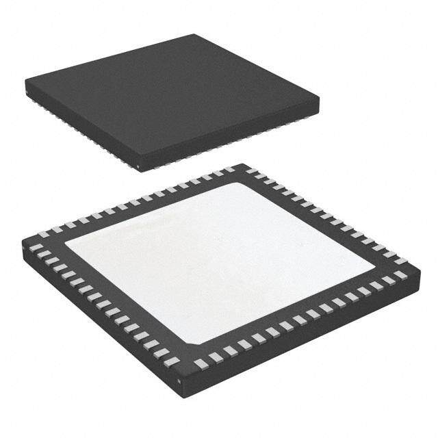
| 产品图片 |
|
| rohs | 符合RoHS无铅 / 符合限制有害物质指令(RoHS)规范要求 |
| 产品系列 | 数据转换器IC,模数转换器 - ADC,Texas Instruments ADS1220IPW- |
| 数据手册 | |
| 产品型号 | ADS1220IPW |
| 产品种类 | 模数转换器 - ADC |
| 位数 | 24 |
| 供应商器件封装 | 16-TSSOP |
| 其它名称 | 296-36512-5 |
| 分辨率 | 24 bit |
| 包装 | 管件 |
| 商标 | Texas Instruments |
| 安装类型 | 表面贴装 |
| 安装风格 | SMD/SMT |
| 封装 | Tube |
| 封装/外壳 | 16-TSSOP(0.173",4.40mm 宽) |
| 封装/箱体 | TSSOP-16 |
| 工作温度 | -40°C ~ 125°C |
| 工作电源电压 | 2.3 V to 5.5 V |
| 工厂包装数量 | 90 |
| 接口类型 | Serial SPI |
| 数据接口 | SPI |
| 最大功率耗散 | 1.4 mW |
| 最大工作温度 | + 125 C |
| 最小工作温度 | - 40 C |
| 标准包装 | 90 |
| 特性 | PGA, 温度传感器 |
| 特色产品 | http://www.digikey.cn/product-highlights/zh/ads1220-adc-for-small-signal-sensors/50397 |
| 电压参考 | 2.5 V |
| 电压源 | 模拟和数字,双 ± |
| 系列 | ADS1220 |
| 结构 | Delta-Sigma |
| 转换器数 | 1 |
| 转换速率 | 2 kS/s |
| 输入数和类型 | 4 个单端,2 个差分 |
| 输入类型 | Single-Ended/Differential |
| 通道数量 | 4 Channel |
| 采样率(每秒) | 2k |


- 商务部:美国ITC正式对集成电路等产品启动337调查
- 曝三星4nm工艺存在良率问题 高通将骁龙8 Gen1或转产台积电
- 太阳诱电将投资9.5亿元在常州建新厂生产MLCC 预计2023年完工
- 英特尔发布欧洲新工厂建设计划 深化IDM 2.0 战略
- 台积电先进制程称霸业界 有大客户加持明年业绩稳了
- 达到5530亿美元!SIA预计今年全球半导体销售额将创下新高
- 英特尔拟将自动驾驶子公司Mobileye上市 估值或超500亿美元
- 三星加码芯片和SET,合并消费电子和移动部门,撤换高东真等 CEO
- 三星电子宣布重大人事变动 还合并消费电子和移动部门
- 海关总署:前11个月进口集成电路产品价值2.52万亿元 增长14.8%


PDF Datasheet 数据手册内容提取
Product Sample & Technical Tools & Support & Reference Folder Buy Documents Software Community Design ADS1220 SBAS501C–MAY2013–REVISEDAUGUST2016 ADS1220 4-Channel, 2-kSPS, Low-Power, 24-Bit ADC with Integrated PGA and Reference 1 Features 3 Description • LowCurrentConsumption: The ADS1220 is a precision, 24-bit, analog-to-digital 1 converter (ADC) that offers many integrated features AsLowas120μA(typ)inDuty-CycleMode to reduce system cost and component count in • WideSupplyRange:2.3Vto5.5V applications measuring small sensor signals. The • ProgrammableGain:1V/Vto128V/V device features two differential or four single-ended • ProgrammableDataRates:Upto2kSPS inputs through a flexible input multiplexer (MUX), a low-noise, programmable gain amplifier (PGA), two • Upto20-BitsEffectiveResolution programmable excitation current sources, a voltage • Simultaneous50-Hzand60-HzRejectionat reference, an oscillator, a low-side switch, and a 20SPSwithSingle-CycleSettlingDigitalFilter precisiontemperaturesensor. • TwoDifferentialorFourSingle-EndedInputs The device can perform conversions at data rates up • DualMatchedProgrammableCurrentSources: to 2000 samples-per-second (SPS) with single-cycle 10μAto1.5mA settling. At 20 SPS, the digital filter offers simultaneous 50-Hz and 60-Hz rejection for noisy • Internal2.048-VReference:5ppm/°C(typ)Drift industrial applications. The internal PGA offers gains • Internal2%AccurateOscillator upto128V/V.ThisPGAmakestheADS1220ideally- • InternalTemperatureSensor: suited for applications measuring small sensor 0.5°C(typ)Accuracy signals, such as resistance temperature detectors (RTDs), thermocouples, thermistors, and resistive • SPI-CompatibleInterface(Mode1) bridge sensors. The device supports measurements • Package:3.5-mm× 3.5-mm ×0.9-mmVQFN of pseudo- or fully-differential signals when using the PGA. Alternatively, the device can be configured to 2 Applications bypass the internal PGA while still providing high • TemperatureSensorMeasurements: input impedance and gains up to 4 V/V, allowing for single-endedmeasurements. – Thermistors Power consumption is as low as 120 µA when – Thermocouples operating in duty-cycle mode with the PGA disabled. – ResistanceTemperatureDetectors(RTDs): The ADS1220 is offered in a leadless VQFN-16 or a 2-,3-,or4-WireTypes TSSOP-16 package and is specified over a • ResistiveBridgeSensorMeasurements: temperaturerangeof –40°Cto+125°C. – PressureSensors DeviceInformation(1) – StrainGauges PARTNUMBER PACKAGE BODYSIZE(NOM) – WeighScales VQFN(16) 3.50mm×3.50mm • PortableInstrumentation ADS1220 TSSOP(16) 5.00mm×4.40mm • FactoryAutomationandProcessControl (1) For all available packages, see the orderable addendum at theendofthedatasheet. K-TypeThermocoupleMeasurement 3.3 V 3.3 V 0.1 PF 0.1 PF 3.3 V REFP0 REFN0 10 (cid:29)A to AVDD DVDD 1.5 mA AIN0 RIenfteerrennacl e ReMfeUreXnce TI Device Thermocouple AIN1 MUX AINP PGA ß2(cid:8)4(cid:3)A-BDitC DigitaSanPl dFI ilter SCDCSINLK Isothermal Block AAIINN23 AINN TePmSreepcneissraoiotrunr e OLoswci-llDartoiftr Interface DDORDUYT/DRDY AVSS CLK DGND Copyright © 2016, Texas Instruments Incorporated 1 An IMPORTANT NOTICE at the end of this data sheet addresses availability, warranty, changes, use in safety-critical applications, intellectualpropertymattersandotherimportantdisclaimers.PRODUCTIONDATA.
ADS1220 SBAS501C–MAY2013–REVISEDAUGUST2016 www.ti.com Table of Contents 1 Features.................................................................. 1 8.5 Programming...........................................................34 2 Applications........................................................... 1 8.6 RegisterMap...........................................................39 3 Description............................................................. 1 9 ApplicationandImplementation........................ 44 4 RevisionHistory..................................................... 2 9.1 ApplicationInformation............................................44 9.2 TypicalApplications................................................49 5 PinConfigurationandFunctions......................... 4 10 PowerSupplyRecommendations..................... 60 6 Specifications......................................................... 5 10.1 Power-SupplySequencing....................................60 6.1 AbsoluteMaximumRatings......................................5 10.2 Power-SupplyRampRate....................................60 6.2 ESDRatings..............................................................5 10.3 Power-SupplyDecoupling.....................................60 6.3 RecommendedOperatingConditions.......................6 11 Layout................................................................... 61 6.4 ThermalInformation..................................................6 6.5 ElectricalCharacteristics...........................................7 11.1 LayoutGuidelines.................................................61 6.6 SPITimingRequirements.........................................9 11.2 LayoutExample....................................................62 6.7 SPISwitchingCharacteristics...................................9 12 DeviceandDocumentationSupport................. 63 6.8 TypicalCharacteristics............................................10 12.1 DocumentationSupport........................................63 7 ParameterMeasurementInformation................16 12.2 ReceivingNotificationofDocumentationUpdates63 7.1 NoisePerformance.................................................16 12.3 CommunityResources..........................................63 12.4 Trademarks...........................................................63 8 DetailedDescription............................................ 19 12.5 ElectrostaticDischargeCaution............................63 8.1 Overview.................................................................19 12.6 Glossary................................................................63 8.2 FunctionalBlockDiagram.......................................19 13 Mechanical,Packaging,andOrderable 8.3 FeatureDescription.................................................20 Information........................................................... 63 8.4 DeviceFunctionalModes........................................32 4 Revision History NOTE:Pagenumbersforpreviousrevisionsmaydifferfrompagenumbersinthecurrentversion. ChangesfromRevisionB(February2015)toRevisionC Page • ChangedK-TypeThermocoupleMeasurementfigure........................................................................................................... 1 • Addedfootnote1toPinFunctionstableandchangeddescriptionsofAIN0/REFP1,AIN1,AIN2,AIN3/REFN1, REFN0,andREFP0pinsaccordingly.................................................................................................................................... 4 • ChangedFunctionalBlockDiagramfigure........................................................................................................................... 19 • ChangedBypassingthePGAsection.................................................................................................................................. 24 • AddedfourthsentencetoTemperatureSensorsection....................................................................................................... 31 • ChangedlastequationinConvertingfromDigitalCodestoTemperaturesection.............................................................. 31 • Changeddescriptionofbits5:4inConfigurationRegister2................................................................................................ 42 • AddedUnusedInputsandOutputssection ......................................................................................................................... 47 • ChangedFigure74............................................................................................................................................................... 49 • ChangedFigure77............................................................................................................................................................... 52 • ChangedFigure78............................................................................................................................................................... 55 • ChangedFigure79............................................................................................................................................................... 56 • ChangedFigure82............................................................................................................................................................... 58 • ChangedPowerSupplyRecommendationssection:changedPower-SupplySequencingsubsection,addedPower- SupplyRampRatesubsection............................................................................................................................................. 60 2 SubmitDocumentationFeedback Copyright©2013–2016,TexasInstrumentsIncorporated ProductFolderLinks:ADS1220
ADS1220 www.ti.com SBAS501C–MAY2013–REVISEDAUGUST2016 ChangesfromRevisionA(July2013)toRevisionB Page • AddedTIDesign,DeviceInformation,ESDRatings,RecommendedOperatingConditions,andSwitching CharacteristicstablesandApplicationandImplementation,PowerSupplyRecommendations,Layout,Deviceand DocumentationSupport,andMechanical,Packaging,andOrderableInformationsections................................................. 1 • Changeddocumenttitle,QFNtoVQFNthroughoutdocument,Features,Applications,Description,PinConfiguration andFunctions,ParameterMeasurementInformation,FeatureDescription,DeviceFunctionalModes,Programming, andRegisterMapsections,andfront-pagefigure................................................................................................................. 1 • DeletedProductFamilytable ................................................................................................................................................ 4 • ChangedformatofAbsoluteMaximumRatingstable,addedminimumjunctiontemperaturespecification,changed inputcurrentparametername,andremovedmomentaryinputcurrentspecification............................................................ 5 • ChangedAnalogInputsandVoltageReferenceInputssections(specificationvalueswerenotchanged)andadded InternalOscillatorsectiontoElectricalCharacteristicstable.................................................................................................. 7 • ChangedSystemPerformancesection:changedV parameternameandaddedPGAdisabledrowtoOffsetdrift, IO Gainerror,andGaindriftparametersinSystemPerformancesectionofElectricalCharacteristicstable............................7 • ChangedInternalVoltageReferencesection:changedReferencedriftparametermaximumspecificationandadded Long-termdriftparameterinElectricalCharacteristicstable.................................................................................................. 7 • DeletedClockSourcessectionandchangedTemperatureSensorandPowerSupplysections(specificationvalues werenotchanged)inElectricalCharacteristicstable............................................................................................................. 8 • ChangedDigitalInputs/Outputssection,V parameterminimumspecificationinElectricalCharacteristicstable...............8 IL • ChangedSPITimingRequirementsandFigure1(specificationvalueswerenotchanged),addedSPISwitching CharacteristicsandFigure2.................................................................................................................................................. 9 • ChangedformatofTypicalCharacteristicssection(actualcurvesdidnotchange)............................................................ 10 ChangesfromOriginal(May2013)toRevisionA Page • ChangeddocumentstatustoMixedStatus;pre-RTMchangesmadethroughout................................................................ 1 Copyright©2013–2016,TexasInstrumentsIncorporated SubmitDocumentationFeedback 3 ProductFolderLinks:ADS1220
ADS1220 SBAS501C–MAY2013–REVISEDAUGUST2016 www.ti.com 5 Pin Configuration and Functions RVAPackage PWPackage 16-PinVQFN 16-PinTSSOP TopView TopView Y Y D D R R D D K T/ T/ S CL N OU OU C S DI D D SCLK 1 16 DIN 16 15 14 13 CS 2 15 DOUT/DRDY CLK 1 12 DRDY CLK 3 14 DRDY DGND 2 11 DVDD DGND 4 13 DVDD Thermal Pad AVSS 3 10 AVDD AVSS 5 12 AVDD AIN3/REFN1 6 11 AIN0/REFP1 AIN3/REFN1 4 9 AIN0/REFP1 AIN2 7 10 AIN1 5 6 7 8 REFN0 8 9 REFP0 2 0 0 1 N N P N AI EF EF AI R R PinFunctions PIN NO. ANALOGORDIGITAL NAME RVA PW INPUT/OUTPUT DESCRIPTION(1) AIN0/REFP1 9 11 Analoginput Analoginput0,positivereferenceinput1 AIN1 8 10 Analoginput Analoginput1 AIN2 5 7 Analoginput Analoginput2 Analoginput3,negativereferenceinput1. AIN3/REFN1 4 6 Analoginput Internallow-sidepowerswitchconnectedbetweenAIN3/REFN1andAVSS. AVDD 10 12 Analog Positiveanalogpowersupply AVSS 3 5 Analog Negativeanalogpowersupply CLK 1 3 Digitalinput Externalclocksourcepin.ConnecttoDGNDifnotused. CS 16 2 Digitalinput Chipselect;activelow.ConnecttoDGNDifnotused. DGND 2 4 Digital Digitalground DIN 14 16 Digitalinput Serialdatainput DOUT/DRDY 13 15 Digitaloutput Serialdataoutputcombinedwithdataready;activelow Dataready,activelow. DRDY 12 14 Digitaloutput LeaveunconnectedortietoDVDDusingaweakpull-upresistorifnotused. DVDD 11 13 Digital Positivedigitalpowersupply REFN0 6 8 Analoginput Negativereferenceinput0 REFP0 7 9 Analoginput Positivereferenceinput0 SCLK 15 1 Digitalinput Serialclockinput Thermalpad — — Thermalpowerpad.DonotconnectoronlyconnecttoAVSS. (1) SeetheUnusedInputsandOutputssectionforunusedpinconnections. 4 SubmitDocumentationFeedback Copyright©2013–2016,TexasInstrumentsIncorporated ProductFolderLinks:ADS1220
ADS1220 www.ti.com SBAS501C–MAY2013–REVISEDAUGUST2016 6 Specifications 6.1 Absolute Maximum Ratings(1) MIN MAX UNIT AVDDtoAVSS –0.3 7 V Power-supplyvoltage DVDDtoDGND –0.3 7 V AVSStoDGND –2.8 0.3 V Analoginputvoltage AIN0/REFP1,AIN1,AIN2,AIN3/REFN1,REFP0,REFN0 AVSS–0.3 AVDD+0.3 V Digitalinputvoltage CS,SCLK,DIN,DOUT/DRDY,DRDY,CLK DGND–0.3 DVDD+0.3 V Inputcurrent Continuous,anypinexceptpowersupplypins –10 10 mA Junction,T –40 150 °C J Temperature Storage,T –60 150 °C stg (1) StressesbeyondthoselistedunderAbsoluteMaximumRatingsmaycausepermanentdamagetothedevice.Thesearestressratings only,whichdonotimplyfunctionaloperationofthedeviceattheseoranyotherconditionsbeyondthoseindicatedunderRecommended OperatingConditions.Exposuretoabsolute-maximum-ratedconditionsforextendedperiodsmayaffectdevicereliability. 6.2 ESD Ratings VALUE UNIT Human-bodymodel(HBM),perANSI/ESDA/JEDECJS-001(1) ±2000 V Electrostaticdischarge V (ESD) Charged-devicemodel(CDM),perJEDECspecificationJESD22-C101(2) ±500 (1) JEDECdocumentJEP155statesthat500-VHBMallowssafemanufacturingwithastandardESDcontrolprocess. (2) JEDECdocumentJEP157statesthat250-VCDMallowssafemanufacturingwithastandardESDcontrolprocess. Copyright©2013–2016,TexasInstrumentsIncorporated SubmitDocumentationFeedback 5 ProductFolderLinks:ADS1220
ADS1220 SBAS501C–MAY2013–REVISEDAUGUST2016 www.ti.com 6.3 Recommended Operating Conditions overoperatingambienttemperaturerange(unlessotherwisenoted) MIN NOM MAX UNIT POWERSUPPLY AVDDtoAVSS 2.3 5.5 Unipolaranalogpowersupply V AVSStoDGND –0.1 0 0.1 AVDDtoDGND 2.3 2.5 2.75 Bipolaranalogpowersupply V AVSStoDGND –2.75 –2.5 –2.3 Digitalpowersupply DVDDtoDGND 2.3 5.5 V ANALOGINPUTS(1) VIN Differentialinputvoltage VIN=V(AINP)–V(AINN)(2) –Vref/Gain Vref/Gain V PGAdisabled,gain=1to4 AVSS–0.1 AVDD+0.1 V V(AINx) Absoluteinputvoltage PGAenabled,gain=1to128 SeetheLow-NoisePGAsection PGAdisabled,gain=1to4 AVSS–0.1 AVDD+0.1 V VCM Common-modeinputvoltage PGAenabled,gain=1to128 SeetheLow-NoisePGAsection VOLTAGEREFERENCEINPUTS(3) Vref Differentialreferenceinputvoltage Vref=V(REFPx)–V(REFNx) 0.75 2.5 AVDD V V(REFNx) Absolutenegativereferencevoltage AVSS–0.1 V(REFPx)–0.75 V V(REFPx) Absolutepositivereferencevoltage V(REFNx)+0.75 AVDD+0.1 V EXTERNALCLOCKSOURCE f(CLK) Externalclockfrequency 0.5 4.096 4.5 MHz Dutycycle 40% 60% DIGITALINPUTS Inputvoltage DGND DVDD V TEMPERATURERANGE TA Operatingambienttemperature –40 125 °C (1) AIN andAIN denotethepositiveandnegativeinputsofthePGA.AINxdenotesoneofthefouravailableanaloginputs. P N PGAdisabledmeansthelow-noisePGAispowereddownandbypassed.Gainsof1,2,and4arestillpossibleinthiscase. SeetheBypassingthePGAsectionformoreinformation. (2) Excludingtheeffectsofoffsetandgainerror. Limitedto±[(AVDD–AVSS)–0.4V]/Gain,whenthePGAisenabled. (3) REFPxandREFNxdenoteoneoftwoavailabledifferentialreferenceinputpairs. 6.4 Thermal Information ADS1220 THERMALMETRIC(1) VQFN(RVA) TSSOP(PW) UNIT 16PINS 16PINS R Junction-to-ambientthermalresistance 43.4 99.5 °C/W θJA R Junction-to-case(top)thermalresistance 47.3 35.2 °C/W θJC(top) R Junction-to-boardthermalresistance 18.4 44.3 °C/W θJB ψ Junction-to-topcharacterizationparameter 0.6 2.4 °C/W JT ψ Junction-to-boardcharacterizationparameter 18.4 43.8 °C/W JB R Junction-to-case(bottom)thermalresistance 2.0 n/a °C/W θJC(bot) (1) Formoreinformationabouttraditionalandnewthermalmetrics,seetheICPackageThermalMetricsapplicationreport(SPRA953). 6 SubmitDocumentationFeedback Copyright©2013–2016,TexasInstrumentsIncorporated ProductFolderLinks:ADS1220
ADS1220 www.ti.com SBAS501C–MAY2013–REVISEDAUGUST2016 6.5 Electrical Characteristics MinimumandmaximumspecificationsapplyfromT =–40°Cto+125°C.TypicalspecificationsareatT =25°C. A A AllspecificationsareatAVDD=3.3V,AVSS=0V,DVDD=3.3V,PGAenabled,DR=20SPS,andexternalV =2.5V ref (unlessotherwisenoted).(1) PARAMETER TESTCONDITIONS MIN TYP MAX UNIT ANALOGINPUTS Absoluteinputcurrent SeetheTypicalCharacteristics Differentialinputcurrent SeetheTypicalCharacteristics SYSTEMPERFORMANCE Resolution(nomissingcodes) 24 Bits Normalmode 20,45,90,175,330,600,1000 DR Datarate Duty-cyclemode 5,11.25,22.5,44,82.5,150,250 SPS Turbomode 40,90,180,350,660,1200,2000 Noise(input-referred) SeetheNoisePerformancesection INL Integralnonlinearity Gain=1to128,VCM=0.5AVDD,bestfit(2) –15 ±6 15 ppmFSR PGAdisabled,gain=1to4,differentialinputs ±4 VIO Inputoffsetvoltage Gain=1,differentialinputs,TA=25°C –30 ±4 30 µV Gain=2to128,differentialinputs ±4 PGAdisabled,gain=1to4 0.25 Offsetdrift Gain=1to128,TA=–40°Cto+85°C(2) 0.08 0.3 µV/°C Gain=1to128 0.25 Offsetmatch Matchbetweenanytwoinputs ±20 µV PGAdisabled,gain=1to4 ±0.015% Gainerror Gain=1to128,TA=25°C –0.1% ±0.015% 0.1% PGAdisabled,gain=1to4 1 Gaindrift ppm/°C Gain=1to128(2) 1 4 50Hz±3%,DR=20SPS,externalCLK, 105 50/60bit=10 NMRR Normal-moderejectionratio(2) 60Hz±3%,DR=20SPS,externalCLK, 105 dB 50/60bit=11 50Hzor60Hz±3%,DR=20SPS, 90 externalCLK,50/60bit=01 Atdc,gain=1 90 105 CMRR Common-moderejectionratio f(CM)=50Hz,DR=2000SPS(2) 95 115 dB f(CM)=60Hz,DR=2000SPS(2) 95 115 AVDDatdc,VCM=0.5AVDD,gain=1 80 105 PSRR Power-supplyrejectionratio dB DVDDatdc,VCM=0.5AVDD,gain=1(2) 100 115 INTERNALVOLTAGEREFERENCE Initialaccuracy TA=25°C 2.045 2.048 2.051 V Referencedrift(2) 5 30 ppm/°C Long-termdrift 1000hours 110 ppm VOLTAGEREFERENCEINPUTS Referenceinputcurrent REFP0=Vref,REFN0=AVSS ±10 nA INTERNALOSCILLATOR Internaloscillatoraccuracy Normalmode –2% ±1% 2% (1) PGAdisabledmeansthelow-noisePGAispowereddownandbypassed.Gainsof1,2,and4arestillpossibleinthiscase. SeetheBypassingthePGAsectionformoreinformation. (2) Minimumandmaximumvaluesareensuredbydesignandcharacterizationdata. Copyright©2013–2016,TexasInstrumentsIncorporated SubmitDocumentationFeedback 7 ProductFolderLinks:ADS1220
ADS1220 SBAS501C–MAY2013–REVISEDAUGUST2016 www.ti.com Electrical Characteristics (continued) MinimumandmaximumspecificationsapplyfromT =–40°Cto+125°C.TypicalspecificationsareatT =25°C. A A AllspecificationsareatAVDD=3.3V,AVSS=0V,DVDD=3.3V,PGAenabled,DR=20SPS,andexternalV =2.5V ref (unlessotherwisenoted).(1) PARAMETER TESTCONDITIONS MIN TYP MAX UNIT EXCITATIONCURRENTSOURCES(IDACs) Currentsettings 10,50,100,250,500,1000,1500 µA Compliancevoltage Allcurrentsettings AVDD–0.9 V Accuracy Allcurrentsettings,eachIDAC –6% ±1% 6% Currentmatch BetweenIDACs(notvalidfor10-µAsetting) ±0.3% Temperaturedrift EachIDAC(notvalidfor10-µAsetting) 50 ppm/°C Temperaturedriftmatching BetweenIDACs(notvalidfor10-µAsetting) 10 ppm/°C TEMPERATURESENSOR Conversionresolution 14 Bits Temperatureresolution 0.03125 °C TA=0°Cto+75°C –0.5 ±0.25 0.5 Accuracy °C TA=–40°Cto+125°C –1 ±0.5 1 Accuracyvsanalogsupplyvoltage 0.0625 0.25 °C/V LOW-SIDEPOWERSWITCH RON On-resistance 3.5 5.5 Ω Currentthroughswitch 30 mA DIGITALINPUTS/OUTPUTS VIH High-levelinputvoltage 0.7DVDD DVDD V VIL Low-levelinputvoltage DGND 0.3DVDD V VOH High-leveloutputvoltage IOH=3mA 0.8DVDD V VOL Low-leveloutputvoltage IOL=3mA 0.2DVDD V IH Inputleakage,high VIH=5.5V –10 10 µA IL Inputleakage,low VIL=DGND –10 10 µA POWERSUPPLY Power-downmode 0.1 3 Duty-cyclemode,PGAdisabled 65 Duty-cyclemode,gain=1to16 95 Duty-cyclemode,gain=32 115 Duty-cyclemode,gain=64,128 135 Normalmode,PGAdisabled 240 IAVDD Analogsupplycurrent(3) Normalmode,gain=1to16 340 490 µA Normalmode,gain=32 425 Normalmode,gain=64,128 510 Turbomode,PGAdisabled 360 Turbomode,gain=1to16 540 Turbomode,gain=32 715 Turbomode,gain=64,128 890 Power-downmode 0.3 5 Duty-cyclemode 55 IDVDD Digitalsupplycurrent(3) µA Normalmode 75 110 Turbomode 95 Duty-cyclemode,PGAdisabled 0.4 PD Powerdissipation(3) Normalmode,gain=1to16 1.4 mW Turbomode,gain=1to16 2.1 (3) Internalvoltagereferenceselected,internaloscillatorenabled,IDACsturnedoff,andcontinuousconversionmode. Analogsupplycurrentincreasesby70µA,typ(normalmode,turbomode)whenselectinganexternalreference. Analogsupplycurrentincreasesby190µA(typ)whenenablingtheIDACs(excludestheactualIDACcurrent). 8 SubmitDocumentationFeedback Copyright©2013–2016,TexasInstrumentsIncorporated ProductFolderLinks:ADS1220
ADS1220 www.ti.com SBAS501C–MAY2013–REVISEDAUGUST2016 6.6 SPI Timing Requirements overoperatingambienttemperaturerangeandDVDD=2.3Vto5.5V(unlessotherwisenoted) MIN MAX UNIT td(CSSC) Delaytime,CSfallingedgetofirstSCLKrisingedge(1) 50 ns td(SCCS) Delaytime,finalSCLKfallingedgetoCSrisingedge 25 ns tw(CSH) Pulseduration,CShigh 50 ns tc(SC) SCLKperiod 150 ns tw(SCH) Pulseduration,SCLKhigh 60 ns tw(SCL) Pulseduration,SCLKlow 60 ns tsu(DI) Setuptime,DINvalidbeforeSCLKfallingedge 50 ns th(DI) Holdtime,DINvalidafterSCLKfallingedge 25 ns SPItimeout(2) Normalmode,duty-cyclemode 13955 t(MOD) Turbomode 27910 t(MOD) (1) CScanbetiedlowpermanentlyincasetheserialbusisnotsharedwithanyotherdevice. (2) SeetheSPITimeoutsectionformoreinformation. t =1/f .Modulatorfrequencyf =256kHz(normalmode,duty-cyclemode)and512kHz(turbomode),whenusingthe (MOD) (MOD) (MOD) internaloscillatororanexternal4.096-MHzclock. tw(CSH) CS ttd(CSSC)t ttc(SC)t tw(SCH) ttd(SCCS)t SCLK tsu(DI) th(DI) tw(SCL) DIN NOTE:Single-bytecommunicationisshown.Actualcommunicationmaybemultiplebytes. Figure1. SerialInterfaceTimingRequirements 6.7 SPI Switching Characteristics overoperatingambienttemperaturerange,DVDD=2.3Vto5.5V(unlessotherwisenoted) PARAMETER TESTCONDITIONS MIN TYP MAX UNIT Propagationdelaytime, tp(CSDO) CSfallingedgetoDOUTdriven DOUTload=20pF||10kΩtoDGND 50 ns Propagationdelaytime, tp(SCDO) SCLKrisingedgetovalidnewDOUT DOUTload=20pF||10kΩtoDGND 0 50 ns Propagationdelaytime, tp(CSDOZ) CSrisingedgetoDOUThighimpedance DOUTload=20pF||10kΩtoDGND 50 ns CS SCLK tp(CSDO) tp(SCDO) tp(CSDOZ) Hi-Z Hi-Z DOUT/DRDY NOTE:Single-bytecommunicationisshown.Actualcommunicationmaybemultiplebytes. Figure2. SerialInterfaceSwitchingCharacteristics Copyright©2013–2016,TexasInstrumentsIncorporated SubmitDocumentationFeedback 9 ProductFolderLinks:ADS1220
ADS1220 SBAS501C–MAY2013–REVISEDAUGUST2016 www.ti.com 6.8 Typical Characteristics AtT =25°C,AVDD=3.3V,AVSS=0V,andPGAenabledusingexternalV =2.5V(unlessotherwisenoted). A ref 40 40 Gain = 1 Gain = 1 Gain = 128 Gain = 128 30 PGA Disabled 30 PGA Disabled V) V) µ µ e ( 20 e ( 20 g g a a olt olt V V et 10 et 10 s s Off Off 0 0 –10 –10 –40 –20 0 20 40 60 80 100 120 –40 –20 0 20 40 60 80 100 120 Temperature ((cid:131)C) C017 Temperature ((cid:131)C) C018 AVDD=3.3V AVDD=5.0V Figure3.Input-ReferredOffsetVoltagevsTemperature Figure4.Input-ReferredOffsetVoltagevsTemperature 500 500 Gain = 1 Gain = 1 Gain = 128 Gain = 128 S) 400 PGA Disabled S) 400 PGA Disabled F F of of m 300 m 300 p p p p or ( or ( Err200 Err200 n n ai ai G G 100 100 0 0 –40 –20 0 20 40 60 80 100 120 –40 –20 0 20 40 60 80 100 120 Temperature ((cid:131)C) C019 Temperature ((cid:131)C) C020 AVDD=3.3V AVDD=5.0V Figure5.GainErrorvsTemperature Figure6.GainErrorvsTemperature 15 15 Gain = 1 Gain = 1 Gain = 32 Gain = 32 10 PGA Disabled 10 PGA Disabled S) 5 S) 5 F F of of m 0 m 0 p p p p NL ( –5 NL ( –5 I I –10 –10 –15 –15 –100 –75 –50 –25 0 25 50 75 100 –100 –75 –50 –25 0 25 50 75 100 VIN (% of FS) C025 VIN (% of FS) C029 AVDD=3.3V,external2.5-Vreference,normalmode AVDD=5.0V,external2.5-Vreference,normalmode Figure7.IntegralNonlinearityvs Figure8.IntegralNonlinearityvs DifferentialInputSignal DifferentialInputSignal 10 SubmitDocumentationFeedback Copyright©2013–2016,TexasInstrumentsIncorporated ProductFolderLinks:ADS1220
ADS1220 www.ti.com SBAS501C–MAY2013–REVISEDAUGUST2016 Typical Characteristics (continued) AtT =25°C,AVDD=3.3V,AVSS=0V,andPGAenabledusingexternalV =2.5V(unlessotherwisenoted). A ref 20 20 Gain = 1 Gain = 1 15 Gain = 32 15 Gain = 32 PGA Disabled PGA Disabled 10 10 S) S) F 5 F 5 of of m 0 m 0 p p p p L ( –5 L ( –5 N N I I –10 –10 –15 –15 –20 –20 –100 –75 –50 –25 0 25 50 75 100 –100 –75 –50 –25 0 25 50 75 100 VIN (% of FS) C043 VIN (% of FS) C044 AVDD=3.3V,internalreference,normalmode AVDD=5.0V,internalreference,normalmode Figure9.IntegralNonlinearityvs Figure10.IntegralNonlinearityvs DifferentialInputSignal DifferentialInputSignal 1000 2.051 AVDD = 3.3 V 800 2.050 AVDD = 5.0 V V) e (2.049 Counts 460000 ce Voltag2.048 n e er2.047 ef 200 R 2.046 0 45 46 47 48 49 50 51 2.045 2.0 2.0 2.0 2.0 2.0 2.0 2.0 –40 –20 0 20 40 60 80 100 120 Initial Reference Voltage (V) C042 Temperature ((cid:131)C) C021 T =25°C,datafrom5490devices A Figure11.InternalReferenceVoltageHistogram Figure12.InternalReferenceVoltagevsTemperature 1.00 0 Gain = 1 0.75 –20 Gain = 128 %) 0.50 –40 y Error ( 00..0205 R (dB) ––8600 c R uen –0.25 PS –100 q e Fr –0.50 –120 –0.75 –140 –1.00 –160 –40 –20 0 20 40 60 80 100 120 0.1 1 10 100 1000 Temperature ((cid:131)C) C002 Frequency (kHz) C016 DVDD=3.3V,normalmode Figure13.InternalOscillatorAccuracyvsTemperature Figure14.AVDDPower-SupplyRejectionRatiovs Frequency Copyright©2013–2016,TexasInstrumentsIncorporated SubmitDocumentationFeedback 11 ProductFolderLinks:ADS1220
ADS1220 SBAS501C–MAY2013–REVISEDAUGUST2016 www.ti.com Typical Characteristics (continued) AtT =25°C,AVDD=3.3V,AVSS=0V,andPGAenabledusingexternalV =2.5V(unlessotherwisenoted). A ref 15 15 AIN0 AIN0 AIN1 AIN1 A) 10 AIN2 A) 10 AIN2 n n ent ( 5 AIN3 ent ( 5 AIN3 urr urr C C ut 0 ut 0 p p n n ute I –5 ute I –5 ol ol s s b b A –10 A –10 –15 –15 0.5 1.0 1.5 2.0 2.5 3.0 0.5 1.0 1.5 2.0 2.5 3.0 Absolute Input Voltage V(AINx) (V) C030 Absolute Input Voltage V(AINx) (V) C031 AVDD=3.3V,PGAenabled,T =–40°C AVDD=3.3V,PGAenabled,T =25°C A A Figure15.AbsoluteInputCurrentvs Figure16.AbsoluteInputCurrentvs AbsoluteInputVoltage AbsoluteInputVoltage 20 100 AIN0 AIN0 AIN1 AIN1 10 50 A) AIN2 A) AIN2 n AIN3 n AIN3 nt ( 0 nt ( 0 e e urr –10 urr –50 C C ut ut np –20 np –100 e I e I olut –30 olut –150 s s b b A –40 A –200 –50 –250 0.5 1.0 1.5 2.0 2.5 3.0 0.5 1.0 1.5 2.0 2.5 3.0 Absolute Input Voltage V(AINx) (V) C032 Absolute Input Voltage V(AINx) (V) C033 AVDD=3.3V,PGAenabled,T =85°C AVDD=3.3V,PGAenabled,T =125°C A A Figure17.AbsoluteInputCurrentvs Figure18.AbsoluteInputCurrentvs AbsoluteInputVoltage AbsoluteInputVoltage 40 40 Ta = –40(cid:131)C Ta = –40(cid:131)C Ta = 25°C Ta = 25°C nA) 20 Ta = 85°C nA) 20 Ta = 85°C nt ( Ta = 125°C nt ( Ta = 125°C e e urr 0 urr 0 C C ut ut p p n n al I –20 al I –20 nti nti e e Differ –40 Differ –40 –60 –60 –2.0 –1.5 –1.0 –0.5 0.0 0.5 1.0 1.5 2.0 –2.0 –1.5 –1.0 –0.5 0.0 0.5 1.0 1.5 2.0 Differential Input Voltage VIN (V) C038 Differential Input Voltage VIN (V) C039 AVDD=3.3V,PGAenabled,AIN =AIN0,AIN =AIN1 AVDD=3.3V,PGAenabled,AIN =AIN3,AIN =AIN2 P N P N Figure19.DifferentialInputCurrentvs Figure20.DifferentialInputCurrentvs DifferentialInputVoltage DifferentialInputVoltage 12 SubmitDocumentationFeedback Copyright©2013–2016,TexasInstrumentsIncorporated ProductFolderLinks:ADS1220
ADS1220 www.ti.com SBAS501C–MAY2013–REVISEDAUGUST2016 Typical Characteristics (continued) AtT =25°C,AVDD=3.3V,AVSS=0V,andPGAenabledusingexternalV =2.5V(unlessotherwisenoted). A ref 15 15 AIN0 AIN0 AIN1 AIN1 A) 10 AIN2 A) 10 AIN2 n n ent ( 5 AIN3 ent ( 5 AIN3 urr urr C C ut 0 ut 0 p p n n ute I –5 ute I –5 ol ol s s b b A –10 A –10 –15 –15 0.5 1.0 1.5 2.0 2.5 3.0 0.5 1.0 1.5 2.0 2.5 3.0 Absolute Input Voltage V(AINx) (V) C034 Absolute Input Voltage V(AINx) (V) C035 AVDD=3.3V,PGAdisabled,T =–40°C AVDD=3.3V,PGAdisabled,T =25°C A A Figure21.AbsoluteInputCurrentvs Figure22.AbsoluteInputCurrentvs AbsoluteInputVoltage AbsoluteInputVoltage 20 100 AIN0 AIN0 AIN1 AIN1 10 50 A) AIN2 A) AIN2 n AIN3 n AIN3 nt ( 0 nt ( 0 e e urr –10 urr –50 C C ut ut np –20 np –100 e I e I olut –30 olut –150 s s b b A –40 A –200 –50 –250 0.5 1.0 1.5 2.0 2.5 3.0 0.5 1.0 1.5 2.0 2.5 3.0 Absolute Input Voltage V(AINx) (V) C036 Absolute Input Voltage V(AINx) (V) C037 AVDD=3.3V,PGAdisabled,T =85°C AVDD=3.3V,PGAdisabled,T =125°C A A Figure23.AbsoluteInputCurrentvs Figure24.AbsoluteInputCurrentvs AbsoluteInputVoltage AbsoluteInputVoltage 40 40 Ta = –40(cid:131)C Ta = –40(cid:131)C Ta = 25°C Ta = 25°C nA) 20 Ta = 85°C nA) 20 Ta = 85°C nt ( Ta = 125°C nt ( Ta = 125°C e e urr 0 urr 0 C C ut ut p p n n al I –20 al I –20 nti nti e e Differ –40 Differ –40 –60 –60 –2.0 –1.5 –1.0 –0.5 0.0 0.5 1.0 1.5 2.0 –2.0 –1.5 –1.0 –0.5 0.0 0.5 1.0 1.5 2.0 Differential Input Voltage VIN (V) C040 Differential Input Voltage VIN (V) C041 AVDD=3.3V,PGAdisabled,AIN =AIN0,AIN =AIN1 AVDD=3.3V,PGAdisabled,AIN =AIN3,AIN =AIN2 P N P N Figure25.DifferentialInputCurrentvs Figure26.DifferentialInputCurrentvs DifferentialInputVoltage DifferentialInputVoltage Copyright©2013–2016,TexasInstrumentsIncorporated SubmitDocumentationFeedback 13 ProductFolderLinks:ADS1220
ADS1220 SBAS501C–MAY2013–REVISEDAUGUST2016 www.ti.com Typical Characteristics (continued) AtT =25°C,AVDD=3.3V,AVSS=0V,andPGAenabledusingexternalV =2.5V(unlessotherwisenoted). A ref 6 6 IDAC = 1000 µA 4 IDAC = 500 µA 4 IDAC = 100 µA %) or (%) 2 C Error ( 2 IDAC Err–20 olute IDA–20 s b A –4 –4 –6 –6 0.5 0.6 0.7 0.8 0.9 1.0 –40 –20 0 20 40 60 80 100 120 Compliance Voltage (V) C006 Temperature ((cid:131)C) C005 Figure27.IDACAccuracyvsComplianceVoltage Figure28.IDACAccuracyvsTemperature 1.00 600 IDAC = 1000 µA 0.75 IDAC = 500 µA 500 %) 0.50 IDAC = 100 µA or ( 400 g Err 0.25 µA) Matchin –00..2050 I (AVDD300 C 200 A –0.50 Gain = 64, 128 D I –0.75 100 Gain = 1 to 16 PGA Disabled –1.00 0 –40 –20 0 20 40 60 80 100 120 –40 –20 0 20 40 60 80 100 120 Temperature ((cid:131)C) C007 Temperature ((cid:131)C) C011 AVDD=3.3V,internalreference,normalmode Figure29.IDACMatchingvsTemperature Figure30.I vsTemperature AVDD 1000 150 125 800 100 A) 600 A) µ µ (D (D 75 D D IAV 400 IAV 50 Gain = 64, 128 Gain = 64, 128 200 Gain = 1 to 16 25 Gain = 1 to 16 PGA Disabled PGA Disabled 0 0 –40 –20 0 20 40 60 80 100 120 –40 –20 0 20 40 60 80 100 120 Temperature ((cid:131)C) C012 Temperature ((cid:131)C) C013 AVDD=3.3V,internalreference,turbomode AVDD=3.3V,internalreference,duty-cyclemode Figure31.I vsTemperature Figure32.I vsTemperature AVDD AVDD 14 SubmitDocumentationFeedback Copyright©2013–2016,TexasInstrumentsIncorporated ProductFolderLinks:ADS1220
ADS1220 www.ti.com SBAS501C–MAY2013–REVISEDAUGUST2016 Typical Characteristics (continued) AtT =25°C,AVDD=3.3V,AVSS=0V,andPGAenabledusingexternalV =2.5V(unlessotherwisenoted). A ref 600 120 500 100 400 80 A) A) µ µ (D300 (D 60 D D IAV IDV 200 40 Gain = 64, 128 Turbo Mode 100 Gain = 1 to 16 20 Normal Mode PGA Disabled Duty-Cycle Mode 0 0 2.5 3.0 3.5 4.0 4.5 5.0 5.5 2.5 3.0 3.5 4.0 4.5 5.0 5.5 AVDD (V) C004 DVDD (V) C010 Normalmode,internalreference Figure33.I vsAVDD Figure34.I vsDVDD AVDD DVDD 120 1.00 Mean + 61 100 0.75 Mean C) 0.50 Mean - 61 I (µA) DVDD 6800 (cid:131)erature Error ( –000...202505 40 p m Turbo Mode Te –0.50 20 Normal Mode –0.75 Duty-Cycle Mode 0 –1.00 –40 –20 0 20 40 60 80 100 120 –40 –20 0 20 40 60 80 100 120 Temperature ((cid:131)C) C014 Temperature ((cid:131)C) C015 DVDD=3.3V Figure35.I vsTemperature Figure36.InternalTemperatureSensorAccuracyvs DVDD Temperature 6 5 4 (cid:13) (cid:12) (N3 O R 2 AVDD = 2.3 V 1 AVDD = 3.3 V AVDD = 5.0 V 0 –40 –20 0 20 40 60 80 100 120 Temperature ((cid:131)C) C001 Figure37.Low-SidePowerSwitchR vsTemperature ON Copyright©2013–2016,TexasInstrumentsIncorporated SubmitDocumentationFeedback 15 ProductFolderLinks:ADS1220
ADS1220 SBAS501C–MAY2013–REVISEDAUGUST2016 www.ti.com 7 Parameter Measurement Information 7.1 Noise Performance Delta-sigma (ΔΣ) analog-to-digital converters (ADCs) are based on the principle of oversampling. The input signal of a ΔΣ ADC is sampled at a high frequency (modulator frequency) and subsequently filtered and decimated in the digital domain to yield a conversion result at the respective output data rate. The ratio between modulator frequency and output data rate is called oversampling ratio (OSR). By increasing the OSR, and thus reducing the output data rate, the noise performance of the ADC can be optimized. In other words, the input- referred noise drops when reducing the output data rate because more samples of the internal modulator are averaged to yield one conversion result. Increasing the gain also reduces the input-referred noise, which is particularlyusefulwhenmeasuringlow-levelsignals. Table 1 to Table 8 summarize the device noise performance. Data are representative of typical noise performance at T = 25°C using the internal 2.048-V reference. Data shown are the result of averaging readings A from a single device over a time period of approximately 0.75 seconds and are measured with the inputs internallyshortedtogether.Table1,Table3,Table5andTable7listtheinput-referrednoiseinunitsof μV for RMS the conditions shown. Note that µV values are shown in parenthesis. Table 2, Table 4, Table 6and Table 8 list PP the corresponding data in effective number of bits (ENOB) calculated from μV values using Equation 1. Note RMS thatnoise-freebitscalculatedfrompeak-to-peaknoisevaluesusingEquation2areshowninparenthesis. Theinput-referrednoise(Table1,Table3,Table5andTable7)onlychangesmarginallywhenusinganexternal low-noise reference, such as the REF5020. To calculate ENOB numbers and noise-free bits when using a referencevoltageotherthan2.048V,useEquation1 toEquation3: ENOB=ln(Full-ScaleRange/V )/ln(2) (1) RMS-Noise Noise-FreeBits=ln(Full-ScaleRange/V )/ln(2) (2) PP-Noise Full-ScaleRange=2·V /Gain (3) ref Table1.NoiseinμV (μV ) RMS PP atAVDD=3.3V,AVSS=0V,NormalMode,andInternalReference=2.048V DATA GAIN(PGAEnabled) RATE (SPS) 1 2 4 8 16 32 64 128 20 3.71(13.67) 1.54(5.37) 1.15(4.15) 0.80(3.36) 0.35(1.16) 0.23(0.73) 0.10(0.35) 0.09(0.41) 45 7.36(29.54) 2.93(13.06) 1.71(9.28) 0.88(4.06) 0.50(2.26) 0.29(1.49) 0.19(0.82) 0.12(0.51) 90 10.55(47.36) 4.50(20.75) 2.43(11.35) 1.51(6.65) 0.65(3.62) 0.42(2.14) 0.27(1.22) 0.18(0.85) 175 11.90(63.72) 6.45(34.06) 3.26(17.76) 1.82(11.20) 1.01(5.13) 0.57(3.09) 0.34(2.14) 0.26(1.60) 330 19.19(106.93) 9.38(50.78) 4.25(26.25) 2.68(14.13) 1.45(7.52) 0.79(4.66) 0.50(2.69) 0.34(1.99) 600 24.78(151.61) 13.35(72.27) 6.68(39.43) 3.66(19.26) 2.10(12.77) 1.14(6.87) 0.70(4.76) 0.55(3.34) 1000 37.53(227.29) 18.87(122.68) 9.53(58.53) 5.37(31.52) 2.95(18.08) 1.65(10.71) 1.03(6.52) 0.70(4.01) Table2.ENOBfromRMSNoise(Noise-FreeBitsfromPeak-to-PeakNoise) atAVDD=3.3V,AVSS=0V,NormalMode,andInternalReference=2.048V DATA GAIN(PGAEnabled) RATE (SPS) 1 2 4 8 16 32 64 128 20 20.08(18.19) 20.34(18.54) 19.76(17.91) 19.28(17.22) 19.48(17.75) 19.10(17.42) 19.33(17.49) 18.49(16.26) 45 19.09(17.08) 19.42(17.26) 19.19(16.75) 19.15(16.94) 18.95(16.79) 18.74(16.39) 18.38(16.25) 18.00(15.49) 90 18.57(16.40) 18.80(16.59) 18.68(16.46) 18.37(16.23) 18.60(16.11) 18.20(15.87) 17.87(15.67) 17.44(15.20) 175 18.39(15.97) 18.28(15.88) 18.26(15.82) 18.10(15.48) 17.96(15.61) 17.78(15.34) 17.53(14.87) 16.91(14.29) 330 17.70(15.23) 17.74(15.30) 17.88(15.25) 17.54(15.15) 17.43(15.05) 17.30(14.74) 16.96(14.54) 16.50(13.97) 600 17.33(14.72) 17.23(14.79) 17.23(14.66) 17.09(14.70) 16.89(14.29) 16.77(14.18) 16.48(13.72) 15.83(13.23) 1000 16.74(14.14) 16.73(14.03) 16.71(14.09) 16.54(13.99) 16.41(13.79) 16.25(13.54) 15.92(13.26) 15.49(12.96) 16 SubmitDocumentationFeedback Copyright©2013–2016,TexasInstrumentsIncorporated ProductFolderLinks:ADS1220
ADS1220 www.ti.com SBAS501C–MAY2013–REVISEDAUGUST2016 Table3.NoiseinμV (μV )withPGADisabled RMS PP atAVDD=3.3V,AVSS=0V,NormalMode,andInternalReference=2.048V GAIN(PGADisabled) DATARATE (SPS) 1 2 4 20 3.89(13.43) 1.85(6.84) 1.26(3.91) 45 6.97(31.98) 2.94(12.94) 1.41(5.62) 90 8.50(42.48) 4.49(18.92) 2.07(9.95) 175 12.99(65.92) 6.24(35.40) 3.04(18.92) 330 18.18(94.24) 8.12(50.17) 4.71(28.75) 600 25.29(138.67) 12.77(78.13) 6.27(39.79) 1000 38.04(260.50) 18.40(120.97) 9.48(63.72) Table4.ENOBfromRMSNoise(Noise-FreeBitsfromPeak-to-PeakNoise)withPGADisabled atAVDD=3.3V,AVSS=0V,NormalMode,andInternalReference=2.048V GAIN(PGADisabled) DATARATE (SPS) 1 2 4 20 20.01(18.22) 20.08(18.19) 19.63(18.00) 45 19.61(16.97) 19.41(17.27) 19.47(17.48) 90 18.88(16.56) 18.80(16.72) 18.91(16.65) 175 18.27(15.92) 18.32(15.82) 18.36(15.72) 330 17.78(15.41) 17.94(15.32) 17.73(15.12) 600 17.31(14.85) 17.29(14.68) 17.32(14.65) 1000 16.72(13.94) 16.76(14.05) 16.72(13.97) Table5.NoiseinμV (μV ) RMS PP atAVDD=3.3V,AVSS=0V,TurboMode,andInternalReference=2.048V DATA GAIN(PGAEnabled) RATE (SPS) 1 2 4 8 16 32 64 128 40 4.56(24.17) 2.40(11.35) 1.22(4.94) 0.71(2.84) 0.35(1.60) 0.19(0.85) 0.16(0.71) 0.09(0.55) 90 5.74(25.88) 2.97(14.40) 1.47(5.80) 1.13(5.52) 0.50(2.67) 0.32(1.32) 0.23(1.13) 0.15(0.69) 180 8.49(46.88) 4.66(21.36) 2.30(12.88) 1.24(7.23) 0.72(4.82) 0.42(2.57) 0.28(1.47) 0.24(1.34) 350 13.42(84.72) 5.86(40.04) 3.39(19.04) 1.88(10.13) 1.05(6.15) 0.64(3.59) 0.43(2.29) 0.28(1.39) 660 17.09(120.36) 9.34(47.36) 4.81(27.83) 2.97(17.36) 1.54(10.21) 0.82(4.43) 0.58(3.67) 0.41(2.93) 1200 25.71(162.35) 12.31(85.94) 6.81(44.01) 3.72(21.55) 2.09(15.14) 1.23(7.58) 0.80(5.31) 0.57(3.51) 2000 36.23(265.14) 18.24(127.32) 9.24(65.43) 5.49(37.02) 2.89(18.89) 1.77(12.00) 1.13(7.60) 0.82(5.81) Table6.ENOBfromRMSNoise(Noise-FreeBitsfromPeak-to-PeakNoise) atAVDD=3.3V,AVSS=0V,TurboMode,andInternalReference=2.048V DATA GAIN(PGAEnabled) RATE (SPS) 1 2 4 8 16 32 64 128 40 19.78(17.37) 19.71(17.46) 19.68(17.66) 19.45(17.46) 19.47(17.29) 19.37(17.21) 18.65(16.46) 18.40(15.83) 90 19.45(17.27) 19.39(17.12) 19.41(17.43) 18.79(16.50) 18.97(16.55) 18.62(16.57) 18.11(15.80) 17.75(15.49) 180 18.88(16.42) 18.75(16.55) 18.76(16.28) 18.65(16.11) 18.43(15.70) 18.23(15.60) 17.79(15.41) 17.05(14.54) 350 18.22(15.56) 18.42(15.64) 18.21(15.71) 18.05(15.62) 17.89(15.35) 17.62(15.12) 17.20(14.77) 16.78(14.49) 660 17.87(15.05) 17.74(15.40) 17.70(15.17) 17.39(14.85) 17.34(14.61) 17.25(14.82) 16.75(14.09) 16.25(13.42) 1200 17.28(14.62) 17.34(14.54) 17.20(14.51) 17.07(14.54) 16.90(14.05) 16.67(14.04) 16.28(13.56) 15.77(13.15) 2000 16.79(13.92) 16.78(13.97) 16.76(13.93) 16.51(13.76) 16.44(13.73) 16.14(13.38) 15.79(13.04) 15.25(12.43) Copyright©2013–2016,TexasInstrumentsIncorporated SubmitDocumentationFeedback 17 ProductFolderLinks:ADS1220
ADS1220 SBAS501C–MAY2013–REVISEDAUGUST2016 www.ti.com Table7.NoiseinμV (μV )withPGADisabled RMS PP atAVDD=3.3V,AVSS=0V,TurboMode,andInternalReference=2.048V GAIN(PGADisabled) DATARATE (SPS) 1 2 4 40 4.22(22.46) 2.30(10.74) 0.93(3.91) 90 6.57(31.01) 3.53(14.28) 1.59(6.84) 180 8.41(55.66) 4.30(22.09) 2.31(14.59) 350 12.68(75.20) 6.02(34.18) 3.22(17.64) 660 17.81(111.08) 9.06(56.76) 4.24(27.47) 1200 25.43(176.03) 12.70(89.23) 6.28(40.95) 2000 36.11(250.98) 17.30(131.35) 8.77(68.18) Table8.ENOBfromRMSNoise(Noise-FreeBitsfromPeak-to-PeakNoise)withPGADisabled atAVDD=3.3V,AVSS=0V,TurboMode,andInternalReference=2.048V GAIN(PGADisabled) DATARATE (SPS) 1 2 4 40 19.89(17.48) 19.76(17.54) 20.07(18.00) 90 19.25(17.01) 19.15(17.13) 19.29(17.19) 180 18.89(16.17) 18.86(16.50) 18.76(16.10) 350 18.30(15.73) 18.38(15.87) 18.28(15.83) 660 17.81(15.17) 17.79(15.14) 17.88(15.19) 1200 17.30(14.51) 17.30(14.49) 17.31(14.61) 2000 16.79(13.99) 16.85(13.93) 16.83(13.87) 18 SubmitDocumentationFeedback Copyright©2013–2016,TexasInstrumentsIncorporated ProductFolderLinks:ADS1220
ADS1220 www.ti.com SBAS501C–MAY2013–REVISEDAUGUST2016 8 Detailed Description 8.1 Overview The ADS1220 is a small, low-power, 24-bit, ΔΣ ADC that offers many integrated features to reduce system cost andcomponentcountinapplicationsmeasuringsmallsensorsignals. In addition to the ΔΣ ADC core and single-cycle settling digital filter, the device offers a low-noise, high input impedance, programmable gain amplifier (PGA), an internal voltage reference, and a clock oscillator. The device also integrates a highly linear and accurate temperature sensor as well as two matched programmable current sources (IDACs) for sensor excitation. All of these features are intended to reduce the required external circuitry in typical sensor applications and improve overall system performance. An additional low-side power switch eases the design of low-power bridge sensor applications. The device is fully configured through four registers and controlled by six commands through a mode 1 SPI-compatible interface. The Functional Block Diagram sectionshowsthedevicefunctionalblockdiagram. The ADS1220 ADC measures a differential signal, V , which is the difference in voltage between nodes AIN IN P and AIN . The converter core consists of a differential, switched-capacitor, ΔΣ modulator followed by a digital N filter. The digital filter receives a high-speed bitstream from the modulator and outputs a code proportional to the inputvoltage.Thisarchitectureresultsinaverystrongattenuationofanycommon-modesignal. The device has two available conversion modes: single-shot and continuous conversion mode. In single-shot mode,theADCperformsoneconversionoftheinputsignaluponrequestandstoresthevalueinaninternaldata buffer. The device then enters a low-power state to save power. Single-shot mode is intended to provide significant power savings in systems that require only periodic conversions, or when there are long idle periods between conversions. In continuous conversion mode, the ADC automatically begins a conversion of the input signal as soon as the previous conversion is completed. New data are available at the programmed data rate. Data can be read at any time without concern of data corruption and always reflect the most recently completed conversion. 8.2 Functional Block Diagram AVDD REFP0 REFN0 DVDD 10 (cid:29)A to 1.5 mA Internal Reference AIN0/REFP1 TI Device Reference MUX AIN1 AINP Digital Filter SCCSLK 24-Bit and MUX PGA ß(cid:8)(cid:3)ADC SPI DIN Interface DOUT/DRDY AIN2 AINN DRDY Precision Low-Drift AIN3/REFN1 Temperature Oscillator Sensor AVSS CLK DGND Copyright © 2016, Texas Instruments Incorporated Copyright©2013–2016,TexasInstrumentsIncorporated SubmitDocumentationFeedback 19 ProductFolderLinks:ADS1220
ADS1220 SBAS501C–MAY2013–REVISEDAUGUST2016 www.ti.com 8.3 Feature Description 8.3.1 Multiplexer The device contains a very flexible input multiplexer, as shown in Figure 38. Either four single-ended signals, two differential signals, or a combination of two single-ended signals and one differential signal can be measured. The multiplexer is configured by four bits (MUX[3:0]) in the configuration register. When single-ended signals are measured, the negative ADC input (AIN ) is internally connected to AVSS by a switch within the multiplexer. For N system-monitoring purposes, the analog supply (AVDD – AVSS) / 4 or the currently-selected external reference voltage(V –V )/4canbeselectedasinputstotheADC.Themultiplexeralsooffersthepossibilityto (REFPx) (REFNx) route any of the two programmable current sources to any analog input (AINx) or to any dedicated reference pin (REFP0,REFN0). System Monitors (V(REFPx) – V(REFNx)) / 4 (AVDD – AVSS) / 4 AVDD AVDD IDAC1 IDAC2 (AVDD + AVSS) / 2 AVDD AVSS AIN0/REFP1 AVDD AVSS AVDD AIN1 Burnout Current Source (10 µA) AVDD AVSS AIN2 AVDD AVSS AINP PGA To ADC AINN AIN3/REFN1 AVDD AVSS REFP0 Burnout Current Source (10 µA) AVDD AVSS AVSS AVSS REFN0 Figure38. AnalogInputMultiplexer Electrostatic discharge (ESD) diodes to AVDD and AVSS protect the inputs. To prevent the ESD diodes from turningon,theabsolutevoltageonanyinputmuststaywithintherangeprovidedbyEquation4: AVSS–0.3V<V <AVDD+0.3V (4) (AINx) If the voltages on the input pins have any potential to violate these conditions, external Schottky clamp diodes or series resistors may be required to limit the input current to safe values (see the Absolute Maximum Ratings table). Overdriving an unused input on the device may affect conversions taking place on other input pins. If any overdriveonunusedinputsispossible,TIrecommendsclampingthesignalwithexternalSchottkydiodes. 20 SubmitDocumentationFeedback Copyright©2013–2016,TexasInstrumentsIncorporated ProductFolderLinks:ADS1220
ADS1220 www.ti.com SBAS501C–MAY2013–REVISEDAUGUST2016 Feature Description (continued) 8.3.2 Low-NoisePGA The device features a low-noise, low-drift, high input impedance, programmable gain amplifier (PGA). The PGA can be set to gains of 1, 2, 4, 8, 16, 32, 64, or 128. Three bits (GAIN[2:0]) in the configuration register are used to configure the gain. A simplified diagram of the PGA is shown in Figure 39. The PGA consists of two chopper- stabilized amplifiers (A1 and A2) and a resistor feedback network that sets the PGA gain. The PGA input is equippedwithanelectromagneticinterference(EMI)filter. 200 O AIN + P 25 pF A1 - R F OUT P VIN RG R VOUT = Gain·VIN F OUT N - 200 O A2 AIN + N 25 pF Figure39. SimplifiedPGADiagram V denotes the differential input voltage V = (V – V ). The gain of the PGA can be calculated with IN IN (AINP) (AINN) Equation5: Gain=1+2·R /R (5) F G Gain is changed inside the device using a variable resistor, R . The differential full-scale input voltage range G (FSR)ofthePGAisdefinedbythegainsettingandthereferencevoltageused,asshowninEquation6: FSR=±V /Gain (6) ref Table9showsthecorrespondingfull-scalerangeswhenusingtheinternal2.048-Vreference. Table9.PGAFull-ScaleRange GAINSETTING FSR 1 ±2.048V 2 ±1.024V 4 ±0.512V 8 ±0.256V 16 ±0.128V 32 ±0.064V 64 ±0.032V 128 ±0.016V Copyright©2013–2016,TexasInstrumentsIncorporated SubmitDocumentationFeedback 21 ProductFolderLinks:ADS1220
ADS1220 SBAS501C–MAY2013–REVISEDAUGUST2016 www.ti.com 8.3.2.1 PGACommon-ModeVoltageRequirements To stay within the linear operating range of the PGA, the input signals must meet certain requirements that are discussedinthissection. The outputs of both amplifiers (A1 and A2) in Figure 39 can not swing closer to the supplies (AVSS and AVDD) than 200 mV. If the outputs OUT and OUT are driven to within 200 mV of the supply rails, the amplifiers P N saturate and consequently become nonlinear. To prevent this nonlinear operating condition the output voltages mustmeetEquation7: AVSS+0.2V≤V ,V ≤AVDD–0.2V (7) (OUTN) (OUTP) Translating the requirements of Equation 7 into requirements referred to the PGA inputs (AIN and AIN ) is P N beneficial because there is no direct access to the outputs of the PGA. The PGA employs a symmetrical design, therefore the common-mode voltage at the output of the PGA can be assumed to be the same as the common- modevoltageoftheinputsignal,asshowninFigure40. AIN + P A1 - ½ VIN RF OUTP ½ Gain·V IN VCM = ½ (V(AINP) + V(AINN)) RG ½ Gain·V R IN F ½ VIN OUTN - A2 AIN + N Figure40. PGACommon-ModeVoltage Thecommon-modevoltageiscalculatedusingEquation8: V =½(V +V )=½(V +V ) (8) CM (AINP) (AINN) (OUTP) (OUTN) ThevoltagesatthePGAinputs(AIN andAIN )canbeexpressedasEquation9andEquation10: P N V =V +½V (9) (AINP) CM IN V =V –½V (10) (AINN) CM IN Theoutputvoltages(V andV )canthenbecalculatedasEquation11andEquation12: (OUTP) (OUTN) V =V +½Gain·V (11) (OUTP) CM IN V =V –½Gain·V (12) (OUTN) CM IN The requirements for the output voltages of amplifiers A1 and A2 (Equation 7) can now be translated into requirements for the input common-mode voltage range using Equation 11 and Equation 12, which are given in Equation13andEquation14: V ≥AVSS+0.2V+½Gain·V (13) CM(MIN) IN(MAX) V ≤AVDD–0.2V–½Gain·V (14) CM(MAX) IN(MAX) In order to calculate the minimum and maximum common-mode voltage limits, the maximum differential input voltage (V ) that occurs in the application must be used. V can be less than the maximum possible IN (MAX) IN (MAX) FSvalue. In addition to Equation 13, the minimum V must also meet Equation 15 because of the specific design CM implementationofthePGA. V ≥AVSS+¼(AVDD–AVSS) (15) CM(MIN) 22 SubmitDocumentationFeedback Copyright©2013–2016,TexasInstrumentsIncorporated ProductFolderLinks:ADS1220
ADS1220 www.ti.com SBAS501C–MAY2013–REVISEDAUGUST2016 Figure 41 and Figure 42 show a graphical representation of the common-mode voltage limits for AVDD = 3.3 V andAVSS=0V,withgain=1andgain=16,respectively. 3.30 3.30 2.75 2.75 V) 2.20 V) 2.20 e ( e ( g g n1.65 n1.65 a a RM AVDD / 4 RM AVDD / 4 VC1.10 VC1.10 0.55 0.55 0.00 0.00 0.0 0.5 1.0 1.5 2.0 2.5 3.0 0.00 0.03 0.06 0.09 0.12 0.15 0.18 VIN (V) C009 VIN (V) C008 AVDD=3.3V AVDD=3.3V Figure41.Common-ModeVoltageLimits(Gain=1) Figure42.Common-ModeVoltageLimits(Gain=16) The following discussion explains how to apply Equation 13 through Equation 15 to a hypothetical application. The setup for this example is AVDD = 3.3 V, AVSS = 0 V, and gain = 16, using an external reference, V = 2.5 V. The maximum possible differential input voltage V = (V – V ) that can be applied is then ref IN (AINP) (AINN) limited to the full-scale range of FSR = ±2.5 V / 16 = ±0.156 V. Consequently, Equation 13 through Equation 15 yieldanallowedV rangeof1.45V≤ V ≤ 1.85V. CM CM If the sensor signal connected to the inputs in this hypothetical application does not make use of the entire full- scale range but is limited to V = ±0.1 V, for example, then this reduced input signal amplitude relaxes the IN (MAX) V restrictionto1.0V≤ V ≤ 2.3V. CM CM In the case of a fully-differential sensor signal, each input (AIN , AIN ) can swing up to ±50 mV around the P N common-mode voltage (V + V ) / 2, which must remain between the limits of 1.0 V and 2.3 V. The (AINP) (AINN) output of a symmetrical wheatstone bridge is an example of a fully-differential signal. Figure 43 shows a situation where the common-mode voltage of the input signal is at the lowest limit. V is exactly at 0.2 V in this case. (OUTN) Any further decrease in common-mode voltage (V ) or increase in differential input voltage (V ) drives V CM IN (OUTN) below0.2VandsaturatesamplifierA2. V = 1.05 V + (AINP) A1 - 50 mV R V = 1.8 V F (OUTP) 800 mV V = 1.0 V R/7.5 CM F 800 mV R F 50 mV V(OUTN) = 0.2 V - A2 V = 0.95 V + (AINN) Figure43. ExamplewhereV isatLowestLimit CM Copyright©2013–2016,TexasInstrumentsIncorporated SubmitDocumentationFeedback 23 ProductFolderLinks:ADS1220
ADS1220 SBAS501C–MAY2013–REVISEDAUGUST2016 www.ti.com In contrast, the signal of an RTD is of a pseudo-differential nature (if implemented as shown in the RTD Measurementsection),wherethenegativeinputisheldataconstantvoltageotherthan0Vandonlythevoltage on the positive input changes. When a pseudo-differential signal must be measured, the negative input in this example must be biased at a voltage between 0.95 V and 2.25 V. The positive input can then swing up to V = 100 mV above the negative input. Note that in this case the common-mode voltage changes at the IN (MAX) same time the voltage on the positive input changes. That is, while the input signal swings between 0 V ≤ V ≤ IN V , the common-mode voltage swings between V ≤ V ≤ V + ½ V . Satisfying the IN (MAX) (AINN) CM (AINN) IN (MAX) common-mode voltage requirements for the maximum input voltage V ensures the requirements are met IN (MAX) throughouttheentiresignalrange. Figure44andFigure45showexamplesofbothfully-differentialandpseudo-differentialsignals,respectively. AIN P AIN V P CM 100 mV V 1.0 V CM 100 mV 1.0 V AIN N AIN N 0 V 0 V Figure44.Fully-DifferentialInputSignal Figure45.Pseudo-DifferentialInputSignal NOTE Remember, common-mode voltage requirements with PGA enabled (Equation 13 to Equation15)areasfollows: • V ≥AVSS+ ¼(AVDD – AVSS) CM(MIN) • V ≥AVSS+0.2V+ ½Gain·V CM(MIN) IN(MAX) • V ≤AVDD–0.2V–½Gain·V CM(MAX) IN(MAX) 8.3.2.2 BypassingthePGA At gains of 1, 2, and 4, the device can be configured to disable and bypass the low-noise PGA by setting the PGA_BYPASS bit in the configuration register. Disabling the PGA lowers the overall power consumption and also removes the restrictions of Equation 13 through Equation 15 for the common-mode input voltage range, V . The usable absolute and common-mode input voltage range is (AVSS – 0.1 V ≤ V , V ≤ AVDD + CM (AINx) CM 0.1V)whenthePGAisdisabled. Inordertomeasuresingle-endedsignalsthatarereferencedtoAVSS(AIN =V ,AIN =AVSS),thePGAmust P IN N be bypassed. Configure the device for single-ended measurements by either connecting one of the analog inputs to AVSS externally or by using the internal AVSS connection of the multiplexer (MUX[3:0] settings 1000 through 1011). When configuring the internal multiplexer for settings where AIN = AVSS (MUX[3:0] = 1000 through N 1011) the PGA is automatically bypassed and disabled irrespective of the PGA_BYPASS setting and gain is limitedto1,2,and4.Incasegainissettogreaterthan4,thedevicelimitsgainto4. WhenthePGAisdisabled,thedeviceusesabufferedswitched-capacitorstagetoobtaingainsof1,2,and4.An internal buffer in front of the switched-capacitor stage ensures that the effect on the input loading resulting from the capacitor charging and discharging is minimal. See Figure 21 to Figure 26 for the typical values of absolute input currents (current flowing into or out of each input) and differential input currents (difference in absolute currentbetweenpositiveandnegativeinput)whenthePGAisdisabled. For signal sources with high output impedance, external buffering may still be necessary. Note that active buffers introduce noise and also introduce offset and gain errors. Consider all of these factors in high-accuracy applications. 24 SubmitDocumentationFeedback Copyright©2013–2016,TexasInstrumentsIncorporated ProductFolderLinks:ADS1220
ADS1220 www.ti.com SBAS501C–MAY2013–REVISEDAUGUST2016 8.3.3 Modulator A ΔΣ modulator is used in the ADS1220 to convert the analog input voltage into a pulse code modulated (PCM) data stream. The modulator runs at a modulator clock frequency of f = f / 16 in normal and duty-cycle (MOD) (CLK) mode and f = f / 8 in turbo mode, where f is either provided by the internal oscillator or the external (MOD) (CLK) (CLK) clock source. Table 10 shows the modulator frequency for each operating mode using either the internal oscillatororanexternalclockof4.096MHz. Table10.ModulatorClockFrequencyforDifferent OperatingModes(1) OPERATINGMODE f (MOD) Duty-cyclemode 256kHz Normalmode 256kHz Turbomode 512kHz (1) Usingtheinternaloscillatororanexternal4.096-MHzclock. 8.3.4 DigitalFilter The device uses a linear-phase finite impulse response (FIR) digital filter that performs both filtering and decimation of the digital data stream coming from the modulator. The digital filter is automatically adjusted for the different data rates and always settles within a single cycle. At data rates of 5 SPS and 20 SPS, the filter can be configured to reject 50-Hz or 60-Hz line frequencies or to simultaneously reject 50 Hz and 60 Hz. Two bits (50/60[1:0]) in the configuration register are used to configure the filter accordingly. The frequency responses of the digital filter are illustrated in Figure 46 to Figure 59 for different output data rates using the internal oscillator oranexternal4.096-MHzclock. The filter notches and output data rate scale proportionally with the clock frequency. For example, a notch that appears at 20 Hz when using a 4.096-MHz clock appears at 10 Hz if a 2.048-MHz clock is used. Note that the internal oscillator can vary over temperature as specified in the Electrical Characteristics table. The data rate or conversion time, respectively, and filter notches consequently vary by the same amount. Consider using an externalprecisionclocksourceifadigitalfilternotchataspecificfrequencywithatightertoleranceisrequired. 0 0 –40 –40 B) B) e (d –80 e (d –80 d d u u gnit–120 gnit–120 a a M M –160 –160 –200 –200 0 20 40 60 80 100 120 140 160 180 200 46 48 50 52 54 56 58 60 62 64 Frequency (Hz) Frequency (Hz) C049 C050 Simultaneous50-Hzand60-HzRejection,50/60[1:0]=01 Simultaneous50-Hzand60-HzRejection,50/60[1:0]=01 Figure46.FilterResponse Figure47.DetailedViewofFilterResponse (DR=20SPS) (DR=20SPS) Copyright©2013–2016,TexasInstrumentsIncorporated SubmitDocumentationFeedback 25 ProductFolderLinks:ADS1220
ADS1220 SBAS501C–MAY2013–REVISEDAUGUST2016 www.ti.com 0 0 –40 –40 B) B) e (d –80 e (d –80 d d u u gnit–120 gnit–120 a a M M –160 –160 –200 –200 0 20 40 60 80 100 120 140 160 180 200 46 47 48 49 50 51 52 53 54 Frequency (Hz) Frequency (Hz) C045 C046 50-HzRejectionOnly,50/60[1:0]=10 50-HzRejectionOnly,50/60[1:0]=10 Figure48.FilterResponse Figure49.DetailedViewofFilterResponse (DR=20SPS) (DR=20SPS) 0 0 –40 –40 B) B) e (d –80 e (d –80 d d u u gnit–120 gnit–120 a a M M –160 –160 –200 –200 0 20 40 60 80 100 120 140 160 180 200 56 57 58 59 60 61 62 63 64 Frequency (Hz) Frequency (Hz) C047 C048 60-HzRejectionOnly,50/60[1:0]=11 60-HzRejectionOnly,50/60[1:0]=11 Figure50.FilterResponse Figure51.DetailedViewofFilterResponse (DR=20SPS) (DR=20SPS) 0 0 –20 –20 B) B) d d e ( e ( ud –40 ud–40 nit nit g g a a M M –60 –60 –80 –80 0 20 40 60 80 100 120 140 160 180 200 0 20 40 60 80 100 120 140 160 180 200 Frequency (Hz) C051 Frequency (Hz) C052 50/60[1:0]=00 Figure52.FilterResponse Figure53.FilterResponse (DR=20SPS) (DR=45SPS) 26 SubmitDocumentationFeedback Copyright©2013–2016,TexasInstrumentsIncorporated ProductFolderLinks:ADS1220
ADS1220 www.ti.com SBAS501C–MAY2013–REVISEDAUGUST2016 0 0 –20 –20 B) B) d d e ( e ( ud–40 ud –40 nit nit g g a a M M –60 –60 –80 –80 0 100 200 300 400 500 600 700 800 900 1000 0 100 200 300 400 500 600 700 800 900 1000 Frequency (Hz) C053 Frequency (Hz) C054 Figure54.FilterResponse Figure55.FilterResponse (DR=90SPS) (DR=175SPS) 0 0 –20 –20 B) B) d d e ( e ( ud–40 ud –40 nit nit g g a a M M –60 –60 –80 –80 0 200 400 600 800 10001200 1400 1600 1800 2000 0 500 1000 1500 2000 2500 3000 3500 4000 Frequency (Hz) C055 Frequency (Hz) C056 Figure56.FilterResponse Figure57.FilterResponse (DR=330SPS) (DR=600SPS) 0 0 –20 –20 B) B) d d e ( e ( ud –40 ud –40 nit nit g g a a M M –60 –60 –80 –80 0 1 2 3 4 5 6 7 8 9 10 0 1 2 3 4 5 6 7 8 9 10 Frequency (kHz) C057 Frequency (kHz) C058 Figure58.FilterResponse Figure59.FilterResponse (DR=1kSPS) (DR=2kSPS) Copyright©2013–2016,TexasInstrumentsIncorporated SubmitDocumentationFeedback 27 ProductFolderLinks:ADS1220
ADS1220 SBAS501C–MAY2013–REVISEDAUGUST2016 www.ti.com 8.3.5 OutputDataRate Table 11 shows the actual conversion times for each data rate setting. The values provided are in terms of t (CLK) cycles using an external clock with a clock frequency of f = 4.096 MHz. The data rates scale proportionally in (CLK) caseanexternalclockwithafrequencyotherthan4.096MHzisused. Continuous conversion mode data rates are timed from one DRDY falling edge to the next DRDY falling edge. The first conversion starts 210 · t (normal mode, duty-cycle mode) or 114 · t (turbo mode) after the last (CLK) (CLK) SCLKfallingedgeoftheSTART/SYNCcommand. Single-shot mode data rates are timed from the last SCLK falling edge of the START/SYNC command to the DRDY falling edge and rounded to the next t . In case the internal oscillator is used, an additional oscillator (CLK) wake-uptimeofupto50 µs(normalmode,duty-cyclemode)or25 µs(turbomode)mustbeaddedinsingle-shot mode. The internal oscillator starts to power up at the first SCLK rising edge of the START/SYNC command. If an SCLK frequency higher than 160 kHz (normal mode, duty-cycle mode) or 320 kHz (turbo mode) is used, the oscillator may not be fully powered up at the end of the START/SYNC command. The ADC then waits until the internaloscillatorisfullypoweredupbeforestartingaconversion. Single-shot conversion times in duty-cycle mode are the same as in normal mode. See the Duty-Cycle Mode sectionformoredetailsonduty-cyclemodeoperation. Table11.ConversionTimes NOMINALDATARATE –3-dBBANDWIDTH ACTUALCONVERSIONTIME(t(CLK)) (SPS) (Hz) CONTINUOUSCONVERSIONMODE SINGLE-SHOTMODE NORMALMODE 20 13.1 204768 204850 45 20.0 91120 91218 90 39.6 46128 46226 175 77.8 23664 23762 330 150.1 12464 12562 600 279.0 6896 6994 1000 483.8 4144 4242 DUTY-CYCLEMODE 5 13.1 823120 n/a 11.25 20.0 364560 n/a 22.5 39.6 184592 n/a 44 77.8 94736 n/a 82.5 150.1 49936 n/a 150 279.0 27664 n/a 250 483.8 16656 n/a TURBOMODE 40 26.2 102384 102434 90 39.9 45560 45618 180 79.2 23064 23122 350 155.6 11832 11890 660 300.3 6232 6290 1200 558.1 3448 3506 2000 967.6 2072 2130 Note that even though the conversion time at the 20-SPS setting is not exactly 1 / 20 Hz = 50 ms, this discrepancy does not affect the 50-Hz or 60-Hz rejection. To achieve the 50-Hz and 60-Hz rejection specified in the Electrical Characteristics table, the external clock frequency must be 4.096 MHz. When using the internal oscillator, the conversion time and filter notches vary by the amount specified in the Electrical Characteristics tableforoscillatoraccuracy. 28 SubmitDocumentationFeedback Copyright©2013–2016,TexasInstrumentsIncorporated ProductFolderLinks:ADS1220
ADS1220 www.ti.com SBAS501C–MAY2013–REVISEDAUGUST2016 8.3.6 VoltageReference The device offers an integrated low-drift, 2.048-V reference. For applications that require a different reference voltage value or a ratiometric measurement approach, the device offers two differential reference input pairs (REFP0,REFN0andREFP1,REFN1).Inaddition,theanalogsupply(AVDD)canbeusedasareference. The reference source is selected by two bits (VREF[1:0]) in the configuration register. By default, the internal reference is selected. The internal voltage reference requires less than 25 µs to fully settle after power-up, when comingoutofpower-downmode,orwhenswitchingfromanexternalreferencesourcetotheinternalreference. The differential reference inputs allow freedom in the reference common-mode voltage. REFP0 and REFN0 are dedicated reference inputs whereas REFP1 and REFN1 are shared with inputs AIN0 and AIN3, respectively. All reference inputs are internally buffered to increase input impedance. Therefore, additional reference buffers are usually not required when using an external reference. When used in ratiometric applications, the reference inputs do not load the external circuitry. Note that the analog supply current increases when using an external referencebecausethereferencebuffersareenabled. In most cases the conversion result is directly proportional to the stability of the reference source. Any noise and driftofthevoltagereferenceisreflectedintheconversionresult. 8.3.7 ClockSource The device system clock can either be provided by the internal low-drift oscillator or by an external clock source on the CLK input. Connect the CLK pin to DGND before power-up or reset to activate the internal oscillator. Connecting an external clock to the CLK pin at any time deactivates the internal oscillator after two rising edges on the CLK pin are detected. The device then operates on the external clock. After the ADS1220 switches to the external clock, the device can only be switched back to the internal oscillator by cycling the power supplies or by sendingaRESETcommand. 8.3.8 ExcitationCurrentSources The device provides two matched programmable excitation current sources (IDACs) for RTD applications. The output current of the current sources can be programmed to 10 μA, 50 μA, 100 μA, 250 μA, 500 μA, 1000 μA, or 1500μAusingtherespectivebits(IDAC[2:0])intheconfigurationregister.Eachcurrentsourcecanbeconnected to any of the analog inputs (AINx) as well as to any of the dedicated reference inputs (REFP0 and REFN0). Both current sources can also be connected to the same pin. Routing of the IDACs is configured by bits (I1MUX[2:0], I2MUX[2:0])intheconfigurationregister.CaremustbetakennottoexceedthecompliancevoltageoftheIDACs. Inotherwords,limitthevoltageonthepinwheretheIDACisroutedto ≤ (AVDD – 0.9V),otherwisethespecified accuracy of the IDAC current is not met. For three-wire RTD applications, the matched current sources can be used to cancel errors caused by sensor lead resistance (see the 3-Wire RTD Measurement section for more details). The IDACs require up to 200 µs to start up after the IDAC current is programmed to the respective value using bits IDAC[2:0]. If configuration registers 2 and 3 are not written during the same WREG command, TI recommends to first set the IDAC current to the respective value using bits IDAC[2:0] and thereafter select the routingforeachIDAC(I1MUX[2:0],I2MUX[2:0]). In single-shot mode, the IDACs remain active between any two conversions if the IDAC[2:0] bits are set to a valueotherthan000.However,theIDACsarepowereddownwheneverthePOWERDOWNcommandisissued. Note that the analog supply current increases when enabling the IDACs (that is, when the IDAC[2:0] bits are set to a value other than 000). The IDAC circuit needs this bias current to operate even when the IDACs are not routed to any pin (I1MUX[2:0] = I2MUX[2:0] = 000). In addition, the selected output current is drawn from the analogsupplywhenI1MUX[2:0]orI2MUX[2:0]aresettoavalueotherthan000. 8.3.9 Low-SidePowerSwitch A low-side power switch with low on-resistance connected between the analog input AIN3/REFN1 and AVSS is integrated in the device as well. This power switch can be used to reduce system power consumption in bridge sensor applications by powering down the bridge circuit between conversions. When the respective bit (PSW) in the configuration register is set, the switch automatically closes when the START/SYNC command is sent and opens when the POWERDOWN command is issued. Note that the switch stays closed between conversions in single-shotmodeincasethePSWbitissetto1.TheswitchcanbeopenedatanytimebysettingthePSWbitto 0.Bydefault,theswitchisalwaysopen. Copyright©2013–2016,TexasInstrumentsIncorporated SubmitDocumentationFeedback 29 ProductFolderLinks:ADS1220
ADS1220 SBAS501C–MAY2013–REVISEDAUGUST2016 www.ti.com 8.3.10 SensorDetection To help detect a possible sensor malfunction, the device provides internal 10-µA, burn-out current sources. When enabled by setting the respective bit (BCS) in the configuration register, one current source sources current to the positive analog input (AIN ) currently selected while the other current source sinks current form the P selectednegativeanaloginput(AIN ). N In case of an open circuit in the sensor, these burn-out current sources pull the positive input towards AVDD and the negative input towards AVSS, resulting in a full-scale reading. A full-scale reading may also indicate that the sensor is overloaded or that the reference voltage is absent. A near-zero reading may indicate a shorted sensor. Note that the absolute value of the burn-out current sources typically varies by ±10% and the internal multiplexer adds a small series resistance. Therefore, distinguishing a shorted sensor condition from a normal reading can be difficult, especially if an RC filter is used at the inputs. In other words, even if the sensor is shorted, the voltage drop across the external filter resistance and the residual resistance of the multiplexer causes the output toreadavaluehigherthanzero. Keep in mind that ADC readings of a functional sensor may be corrupted when the burn-out current sources are enabled. TI recommends disabling the burn-out current sources when preforming the precision measurement, andonlyenablingthemtotestforsensorfaultconditions. 8.3.11 SystemMonitor The device provides some means for monitoring the analog power supply and the external voltage reference. To select a monitoring voltage, the internal multiplexer (MUX[3:0]) must be configured accordingly in the configuration register. The device automatically bypasses the PGA and sets the gain to 1, irrespective of the configuration register settings while the monitoring feature is used. Note that the system monitor function only providesacoarseresultandisnotmeanttobeaprecisionmeasurement. Whenmeasuringtheanalogpowersupply(MUX[3:0]=1101),theresultingconversionisapproximately(AVDD – AVSS) / 4. The device uses the internal 2.048-V reference for the measurement regardless of what reference sourceisselectedintheconfigurationregister(VREF[1:0]). When monitoring one of the two possible external reference voltage sources (MUX[3:0] = 1100), the result is approximately (V – V ) / 4. REFPx and REFNx denote the external reference input pair selected in (REFPx) (REFNx) theconfigurationregister(VREF[1:0]).Thedeviceautomaticallyusestheinternalreferenceforthemeasurement. 8.3.12 OffsetCalibration The internal multiplexer offers the option to short both PGA inputs (AIN and AIN ) to mid-supply (AVDD + P N AVSS) / 2. This option can be used to measure and calibrate the device offset voltage by storing the result of the shorted input voltage reading in a microcontroller and consequently subtracting the result from each following reading. TI recommends taking multiple readings with the inputs shorted and averaging the result to reduce the effectofnoise. 30 SubmitDocumentationFeedback Copyright©2013–2016,TexasInstrumentsIncorporated ProductFolderLinks:ADS1220
ADS1220 www.ti.com SBAS501C–MAY2013–REVISEDAUGUST2016 8.3.13 TemperatureSensor The ADS1220 offers an integrated precision temperature sensor. The temperature sensor mode is enabled by setting bit TS = 1 in the configuration register. When in temperature sensor mode, the settings of configuration register 0 have no effect and the device uses the internal reference for measurement, regardless of the selected voltage reference source. Temperature readings follow the same process as the analog inputs for starting and reading conversion results. Temperature data are represented as a 14-bit result that is left-justified within the 24- bit conversion result. Data are output starting with the most significant byte (MSB). When reading the three data bytes, the first 14 bits are used to indicate the temperature measurement result. One 14-bit LSB equals 0.03125°C.Negativenumbersarerepresentedinbinarytwoscomplementformat,asshowninTable12. Table12.14-BitTemperatureDataFormat TEMPERATURE(°C) DIGITALOUTPUT(BINARY) HEX 128 01000000000000 1000 127.96875 00111111111111 0FFF 100 00110010000000 0C80 75 00100101100000 0960 50 00011001000000 0640 25 00001100100000 0320 0.25 00000000001000 0008 0.03125 00000000000001 0001 0 00000000000000 0000 –0.25 11111111111000 3FF8 –25 11110011100000 3CE0 –40 11101100000000 3B00 8.3.13.1 ConvertingfromTemperaturetoDigitalCodes 8.3.13.1.1 ForPositiveTemperatures(forExample,50°C): Twos complement is not performed on positive numbers. Therefore, simply convert the number to binary code in a14-bit,left-justifiedformatwiththeMSB=0todenotethepositivesign. Example:50°C/(0.03125°Cpercount)=1600=0640h=00011001000000 8.3.13.1.2 ForNegativeTemperatures(forExample,–25°C): Generate the twos complement of a negative number by complementing the absolute binary number and adding 1.Then,denotethenegativesignwiththeMSB=1. Example:|–25°C|/(0.03125°Cpercount)=800=0320h=00001100100000 Twoscomplementformat:11110011011111+1=11110011100000 8.3.13.2 ConvertingfromDigitalCodestoTemperature To convert from digital codes to temperature, first check whether the MSB is a 0 or a 1. If the MSB is a 0, simply multiply the decimal code by 0.03125°C to obtain the result. If the MSB = 1, subtract 1 from the result and complementallbits.Then,multiplytheresultby –0.03125°C. Example:Thedevicereadsback0960h:0960hhasanMSB=0. 0960h·0.03125°C=2400 · 0.03125°C=75°C Example:Thedevicereadsback3CE0h:3CE0hhasanMSB=1. Subtract1andcomplementtheresult:3CE0h →0320h 0320h·(–0.03125°C)=800 ·(–0.03125°C)= –25°C Copyright©2013–2016,TexasInstrumentsIncorporated SubmitDocumentationFeedback 31 ProductFolderLinks:ADS1220
ADS1220 SBAS501C–MAY2013–REVISEDAUGUST2016 www.ti.com 8.4 Device Functional Modes 8.4.1 Power-UpandReset When the device powers up, a reset is performed. The reset process takes approximately 50 µs. After this power-up reset time, all internal circuitry (including the voltage reference) are stable and communication with the device is possible. As part of the reset process, the device sets all bits in the configuration registers to the respective default settings. By default, the device is set to single-shot mode. After power-up, the device performs a single conversion using the default register settings and then enters a low-power state. When the conversion is complete, the DRDY pin transitions from high to low. The high-to-low transition of the DRDY pin can be used to signal that the ADS1220 is operational and ready to use. The power-up behavior is intended to prevent systems withtightpower-supplyrequirementsfromencounteringacurrentsurgeduringpower-up. 8.4.2 ConversionModes The device can be operated in one of two conversion modes that can be selected by the CM bit in the configurationregister.Theseconversionmodesaresingle-shotandcontinuousconversionmode. 8.4.2.1 Single-ShotMode In single-shot mode, the device only performs a conversion when a START/SYNC command is issued. The device consequently performs one single conversion and returns to a low-power state afterwards. The internal oscillator and all analog circuitry (except for the excitation current sources) are turned off while the device waits in this low-power state until the next conversion is started. In addition, every write access to any configuration register also starts a new conversion. Writing to any configuration register while a conversion is ongoing functions as a new START/SYNC command that stops the current conversion and restarts a single new conversion. Each conversion is fully settled (assuming the analog input signal settles to its final value before the conversionstarts)becausethedevicedigitalfiltersettleswithinasinglecycle. 8.4.2.2 ContinuousConversionMode In continuous conversion mode, the device continuously performs conversions. When a conversion completes, thedeviceplacestheresultintheoutputbufferandimmediatelybeginsanotherconversion. Inordertostartcontinuousconversionmode,theCMbitmustbesetto1followedbyaSTART/SYNCcommand. The first conversion starts 210 · t (normal mode, duty-cycle mode) or 114 · t (turbo mode) after the last (CLK) (CLK) SCLK falling edge of the START/SYNC command. Writing to any configuration register during an ongoing conversion restarts the current conversion. TI recommends always sending a START/SYNC command immediatelyaftertheCMbitissetto1. 32 SubmitDocumentationFeedback Copyright©2013–2016,TexasInstrumentsIncorporated ProductFolderLinks:ADS1220
ADS1220 www.ti.com SBAS501C–MAY2013–REVISEDAUGUST2016 Device Functional Modes (continued) 8.4.3 OperatingModes In addition to the different conversion modes, the device can also be operated in different operating modes that can be selected to trade-off power consumption, noise performance, and output data rate. These modes are: normalmode,duty-cyclemode,turbomode,andpower-downmode. 8.4.3.1 NormalMode Normalmodeisthedefaultmodeofoperationafterpower-up.Inthismode,theinternalmodulatorofthe ΔΣ ADC runs at a modulator clock frequency of f = f / 16, where the system clock (f ) is either provided by the (MOD) (CLK) (CLK) internal oscillator or the external clock source. The modulator frequency is 256 kHz when using the internal oscillator. Normal mode offers output data rate options ranging from 20 SPS to 1 kSPS with the internal oscillator. The data rate is selected by the DR[2:0] bits in the configuration register. In case an external clock source with a clock frequency other than 4.096 MHz is used, the data rates scale accordingly. For example, usinganexternalclockwithf =2.048MHzyieldsdataratesrangingfrom10SPSto500SPS. (CLK) 8.4.3.2 Duty-CycleMode The noise performance of a ΔΣ ADC generally improves when lowering the output data rate because more samples of the internal modulator can be averaged to yield one conversion result. In applications where power consumption is critical, the improved noise performance at low data rates may not be required. For these applications, the device supports an automatic duty-cycle mode that can yield significant power savings by periodically entering a low-power state between conversions. In principle, the device runs in normal mode with a duty cycle of 25%. This functionality means the device performs one conversion in the same manner as when running in normal mode but then automatically enters a low power-state for three consecutive conversion cycles. The noise performance in duty-cycle mode is therefore comparable to the noise performance in normal mode at fourtimesthedatarate.Dataratesinduty-cyclemoderangefrom5SPSto250SPSwiththeinternaloscillator. 8.4.3.3 TurboMode Applications that require higher data rates up to 2 kSPS can operate the device in turbo mode. In this mode, the internal modulator runs at a higher frequency of f = f / 8. f equals 512 kHz when the internal (MOD) (CLK) (MOD) oscillator or an external 4.096-MHz clock is used. Note that the device power consumption increases because the modulator runs at a higher frequency. Running the ADS1220 in turbo mode at a comparable output data rate as in normal mode yields better noise performance. For example, the input-referred noise at 90 SPS in turbo modeislowerthantheinput-referrednoiseat90SPSinnormalmode. 8.4.3.4 Power-DownMode When the POWERDOWN command is issued, the device enters power-down mode after completing the current conversion. In this mode, all analog circuitry (including the voltage reference and both IDACs) are powered down, the low-side power switch is opened, and the device typically only uses 400 nA of current. While in power- down mode, the device holds the configuration register settings and responds to commands, but does not performanydataconversions. IssuingaSTART/SYNCcommandwakesupthedeviceandeitherstartsasingleconversionorstartscontinuous conversion mode, depending on the conversion mode selected by the CM bit. Note that writing to any configuration register wakes up the device as well, but only starts a single conversion regardless of the selected conversionmode(CM). Copyright©2013–2016,TexasInstrumentsIncorporated SubmitDocumentationFeedback 33 ProductFolderLinks:ADS1220
ADS1220 SBAS501C–MAY2013–REVISEDAUGUST2016 www.ti.com 8.5 Programming 8.5.1 SerialInterface The SPI-compatible serial interface of the device is used to read conversion data, read and write the device configuration registers, and control device operation. Only SPI mode 1 (CPOL = 0, CPHA = 1) is supported. The interface consists of five control lines (CS, SCLK, DIN, DOUT/DRDY, and DRDY) but can be used with only four or even three control signals as well. The dedicated data-ready signal (DRDY) can be configured to be shared with DOUT/DRDY. If the serial bus is not shared with any other device, CS can be tied low permanently so that onlysignalsSCLK,DIN,andDOUT/DRDYarerequiredtocommunicatewiththedevice. 8.5.1.1 ChipSelect(CS) Chip select (CS) is an active-low input that selects the device for SPI communication. This feature is useful when multiple devices share the same serial bus. CS must remain low for the duration of the serial communication. WhenCSistakenhigh,theserialinterfaceisreset,SCLKisignored,andDOUT/DRDYentersahigh-impedance state; as such, DOUT/DRDY cannot indicate when data are ready. In situations where multiple devices are present on the bus, the dedicated DRDY pin can provide an uninterrupted monitor of the conversion status. If the serialbusisnotsharedwithanotherperipheral, CScanbetiedlow. 8.5.1.2 SerialClock(SCLK) The serial clock (SCLK) features a Schmitt-triggered input and is used to clock data into and out of the device on the DIN and DOUT/DRDY pins, respectively. Even though the input has hysteresis, TI recommends keeping the SCLKsignalascleanaspossibletopreventglitchesfromaccidentallyshiftingthedata.Whentheserialinterface isidle,holdSCLKlow. 8.5.1.3 DataReady(DRDY) DRDY indicates when a new conversion result is ready for retrieval. When DRDY falls low, new conversion data are ready. DRDY transitions back high on the next SCLK rising edge. When no data are read during continuous conversion mode, DRDY remains low but pulses high for a duration of 2 · t prior to the next DRDY falling (MOD) edge.TheDRDYpinisalwaysactivelydriven,evenwhenCSishigh. 8.5.1.4 DataInput(DIN) The data input pin (DIN) is used along with SCLK to send data (commands and register data) to the device. The devicelatchesdataonDINontheSCLKfallingedge.ThedeviceneverdrivestheDINpin. 8.5.1.5 DataOutputandDataReady(DOUT/DRDY) DOUT/DRDY serves a dual-purpose function. This pin is used with SCLK to read conversion and register data from the device. Data on DOUT/DRDY are shifted out on the SCLK rising edge. DOUT/DRDY goes to a high- impedancestatewhenCSishigh. In addition, the DOUT/DRDY pin can also be configured as a data-ready indicator by setting the DRDYM bit high in the configuration register. DOUT/DRDY then transitions low at the same time that the DRDY pin goes low to indicate new conversion data are available. Both signals can be used to detect if new data are ready. However, because DOUT/DRDY is disabled when CS is high, the recommended method of monitoring the end of a conversionwhenmultipledevicesarepresentontheSPIbusistousethededicated DRDYpin. 8.5.1.6 SPITimeout The ADS1220 offers an SPI timeout feature that can be used to recover communication when a serial interface transmission is interrupted. This feature is especially useful in applications where CS is permanently tied low and is not used to frame a communication sequence. Whenever a complete command is not sent within 13955 · t (normal mode, duty-cycle mode) or 27910 · t (turbo mode), the serial interface resets and the next (MOD) (MOD) SCLK pulse starts a new communication cycle. See the Modulator section for details on the modulator frequency (f = 1 / t ) in the different operating modes. For the RREG and WREG commands, a complete command (MOD) (MOD) includesthecommandbyteitselfplustheregisterbytesthatarereadorwritten. 34 SubmitDocumentationFeedback Copyright©2013–2016,TexasInstrumentsIncorporated ProductFolderLinks:ADS1220
ADS1220 www.ti.com SBAS501C–MAY2013–REVISEDAUGUST2016 Programming (continued) 8.5.2 DataFormat The device provides 24 bits of data in binary twos complement format. The size of one code (LSB) is calculated usingEquation16. 1LSB=(2·V /Gain)/224=+FS/223 (16) ref A positive full-scale input [V ≥ (+FS – 1 LSB) = (V / Gain – 1 LSB)] produces an output code of 7FFFFFh and IN ref a negative full-scale input (V ≤ –FS = –V / Gain) produces an output code of 800000h. The output clips at IN ref thesecodesforsignalsthatexceedfull-scale. Table13summarizestheidealoutputcodesfordifferentinputsignals. Table13.IdealOutputCodeversusInputSignal INPUTSIGNAL,V IN (AIN –AIN ) IDEALOUTPUTCODE(1) P N ≥FS(223–1)/223 7FFFFFh FS/223 000001h 0 000000h –FS/223 FFFFFFh ≤–FS 800000h (1) Excludestheeffectsofnoise,INL,offset,andgainerrors. MappingoftheanaloginputsignaltotheoutputcodesisshowninFigure60. 7FFFFFh 7FFFFEh ¼ e 000001h d o C 000000h put FFFFFFh ut O ¼ 800001h 800000h ¼ ¼ -FS 0 FS Input Voltage V IN 223-1 223-1 -FS FS 223 223 Figure60. CodeTransitionDiagram Copyright©2013–2016,TexasInstrumentsIncorporated SubmitDocumentationFeedback 35 ProductFolderLinks:ADS1220
ADS1220 SBAS501C–MAY2013–REVISEDAUGUST2016 www.ti.com 8.5.3 Commands The device offers six different commands to control device operation, as shown in Table 14. Four commands are stand-alone instructions (RESET, START/SYNC, POWERDOWN, and RDATA). The commands to read (RREG) and write (WREG) configuration register data from and to the device require additional information as part of the instruction. Table14.CommandDefinitions COMMAND DESCRIPTION COMMANDBYTE(1) RESET Resetthedevice 0000011x START/SYNC Startorrestartconversions 0000100x POWERDOWN Enterpower-downmode 0000001x RDATA Readdatabycommand 0001xxxx RREG Readnnregistersstartingataddressrr 0010rrnn WREG Writennregistersstartingataddressrr 0100rrnn (1) Operands:rr=configurationregister(00to11),nn=numberofbytes–1(00to11),andx=don'tcare. 8.5.3.1 RESET(0000011x) Resets the device to the default values. Wait at least (50 µs + 32 · t ) after the RESET command is sent (CLK) beforesendinganyothercommand. 8.5.3.2 START/SYNC(0000100x) In single-shot mode, the START/SYNC command is used to start a single conversion, or (when sent during an ongoing conversion) to reset the digital filter, and then restarts a single new conversion. When the device is set to continuous conversion mode, the START/SYNC command must be issued one time to start converting continuously. Sending the START/SYNC command while converting in continuous conversion mode resets the digitalfilterandrestartscontinuousconversions. 8.5.3.3 POWERDOWN(0000001x) The POWERDOWN command places the device into power-down mode. This command shuts down all internal analog components, opens the low-side switch, turns off both IDACs, but holds all register values. In case the POWERDOWN command is issued while a conversion is ongoing, the conversion completes before the ADS1220 enters power-down mode. As soon as a START/SYNC command is issued, all analog components returntotheirpreviousstates. 8.5.3.4 RDATA(0001xxxx) The RDATA command loads the output shift register with the most recent conversion result. This command can be used when DOUT/DRDY or DRDY are not monitored to indicate that a new conversion result is available. If a conversion finishes in the middle of the RDATA command byte, the state of the DRDY pin at the end of the read operation signals whether the old or the new result is loaded. If the old result is loaded, DRDY stays low, indicatingthatthenewresultisnotreadout.Thenewconversionresultloadswhen DRDYishigh. 8.5.3.5 RREG(0010rrnn) The RREG command reads the number of bytes specified by nn (number of bytes to be read – 1) from the device configuration register, starting at register address rr. The command is completed after nn + 1 bytes are clocked out after the RREG command byte. For example, the command to read three bytes (nn = 10) starting at configurationregister1(rr=01)is00100110. 8.5.3.6 WREG(0100rrnn) The WREG command writes the number of bytes specified by nn (number of bytes to be written – 1) to the device configuration register, starting at register address rr. The command is completed after nn + 1 bytes are clocked in after the WREG command byte. For example, the command to write two bytes (nn = 01) starting at configuration register 0 (rr = 00) is 0100 0001. The configuration registers are updated on the last SCLK falling edge. 36 SubmitDocumentationFeedback Copyright©2013–2016,TexasInstrumentsIncorporated ProductFolderLinks:ADS1220
ADS1220 www.ti.com SBAS501C–MAY2013–REVISEDAUGUST2016 8.5.4 ReadingData Output pins DRDY and DOUT/DRDY (if the DRDYM bit is set high in the configuration register) transition low when new data are ready for retrieval. The conversion data are written to an internal data buffer. Data can be read directly from this buffer on DOUT/DRDY when DRDY falls low without concern of data corruption. An RDATA command does not have to be sent. Data are shifted out on the SCLK rising edges, MSB first, and consistofthreebytesofdata. Figure 61 to Figure 63 show the timing diagrams for reading conversion data in continuous conversion mode and single-shotmodewhennotusingtheRDATAcommand. CS § § (cid:3) 1 9 17 (cid:3) SCLK § § (cid:3) (cid:3) Hi-Z § § DOUT/DRDY (cid:3) DATA MSB DATA DATA LSB (cid:3) § § (cid:3) (cid:3) § § DRDY (cid:3) (cid:3) Next Data Ready § (cid:3) 2· t (MOD) DIN § § (cid:3) (cid:3) Figure61. ContinuousConversionMode(DRDYM=0) CS § § (cid:3) 1 9 17 (cid:3) SCLK § § (cid:3) (cid:3) Hi-Z § § DOUT/DRDY (cid:3) DATA MSB DATA DATA LSB (cid:3) § § (cid:3) (cid:3) § § DRDY (cid:3) (cid:3) Next Data Ready § (cid:3) 2· t (MOD) DIN § § (cid:3) (cid:3) Figure62. ContinuousConversionMode(DRDYM=1) CS § § (cid:3) 1 (cid:3) 1 9 17 SCLK § § (cid:3) (cid:3) Hi-Z § § DOUT/DRDY (cid:3) (cid:3) DATA MSB DATA DATA LSB § § (cid:3) (cid:3) § § DRDY (cid:3) (cid:3) Next Data Ready § (cid:3) DIN START/SYNC § § (cid:3) (cid:3) Figure63. Single-ShotMode(DRDYM=0) Data can also be read at any time without synchronizing to the DRDY signal using the RDATA command. When an RDATA command is issued, the conversion result currently stored in the data buffer is shifted out on DOUT/DRDY on the following SCLK rising edges. Data can be read continuously with the RDATA command as an alternative to monitoring DRDY or DOUT/DRDY. The DRDY pin can be polled after the LSB is clocked out to determine if a new conversion result was loaded. If a new conversion completes during the read operation but data from the previous conversion are read, then DRDY is low. Otherwise, if the most recent result is read, DRDYishigh.Figure64andFigure65illustratethebehaviorforbothcases. Copyright©2013–2016,TexasInstrumentsIncorporated SubmitDocumentationFeedback 37 ProductFolderLinks:ADS1220
ADS1220 SBAS501C–MAY2013–REVISEDAUGUST2016 www.ti.com CS § § (cid:3) 1 1 9 17 (cid:3) SCLK § § (cid:3) (cid:3) Hi-Z § § DOUT/DRDY (cid:3) DATA MSB DATA DATA LSB (cid:3) § § (cid:3) (cid:3) § DRDY (cid:3) Next Data Ready § (cid:3) DIN RDATA § § (cid:3) (cid:3) Figure64. StateofDRDYwhenaNewConversionFinishesDuringanRDATACommand CS § § (cid:3) 1 1 9 17 (cid:3) SCLK § § (cid:3) (cid:3) Hi-Z § § DOUT/DRDY (cid:3) DATA MSB DATA DATA LSB (cid:3) § § (cid:3) (cid:3) § § DRDY (cid:3) (cid:3) Next Data Ready § (cid:3) DIN RDATA § § (cid:3) (cid:3) Figure65. StateofDRDYwhentheMostRecentConversionResultisReadDuringanRDATACommand 8.5.5 SendingCommands The device serial interface is capable of full-duplex operation while reading conversion data when not using the RDATA command. Full-duplex operation means commands are decoded at the same time that conversion data are read. Commands can be sent on any 8-bit data boundary during a data read operation. When a RREG or RDATA command is recognized, the current data read operation is aborted and the conversion data are corrupted, unless the command is sent while the last byte of the conversion result is retrieved. The device starts tooutputtherequesteddataonDOUT/DRDYatthefirstSCLKrisingedgeafterthecommandbyte.Toreaddata withoutinterruption,keepDINlowwhileclockingoutdata. A WREG command can be sent without corrupting an ongoing read operation. Figure 66 shows an example for sending a WREG command to write two configuration registers while reading conversion data in continuous conversion mode. After the command is clocked in (after the 32nd SCLK falling edge), the device resets the digital filter and starts converting with the new register settings. The WREG command can be sent on any of the 8-bitboundaries. CS § § (cid:3) 1 9 17 25 (cid:3) SCLK § § (cid:3) (cid:3) Hi-Z § § DOUT/DRDY (cid:3) DATA MSB DATA DATA LSB (cid:3) § (cid:3) § § DRDY (cid:3) (cid:3) Next Data Ready § (cid:3) 2· t (MOD) DIN WREG REG_DATA REG_DATA § § (cid:3) (cid:3) Figure66. ExampleofReadingDatawhileSimultaneouslySendingaWREGCommand Note that the serial interface does not decode commands while an RDATA or RREG command is executed. That is, all 24 bits of the conversion result must be read after the RDATA command is issued and all requested registersmustbereadafteraRREGcommandissentbeforeanewcommandcanbeissued. 38 SubmitDocumentationFeedback Copyright©2013–2016,TexasInstrumentsIncorporated ProductFolderLinks:ADS1220
ADS1220 www.ti.com SBAS501C–MAY2013–REVISEDAUGUST2016 8.5.6 InterfacingwithMultipleDevices When connecting multiple ADS1220 devices to a single SPI bus, SCLK, DIN, and DOUT/DRDY can be safely shared by using a dedicated chip-select (CS) line for each SPI-enabled device. When CS transitions high for the respective device, DOUT/DRDY enters a 3-state mode. Therefore, DOUT/DRDY cannot be used to indicate when new data are available if CS is high, regardless of the DRDYM bit setting in the configuration register. Only the dedicated DRDY pin indicates that new data are available, because the DRDY pin is actively driven even whenCSishigh. In some cases the DRDY pin cannot be interfaced to the microcontroller. This scenario can occur if there are insufficient GPIO channels available on the microcontroller or if the serial interface must be galvanically isolated and thus the amount of channels must be limited. Therefore, in order to evaluate when a new conversion of one of the devices is ready, the microcontroller can periodically drop CS to the respective device and poll the state of the DOUT/DRDY pin. When CS goes low, the DOUT/DRDY pin immediately drives either high or low, provided that the DRDYM bit is configured to 1. If the DOUT/DRDY line drives low, when CS is taken low, new data are currently available. If the DOUT/DRDY line drives high, no new data are available. This procedure requires that DOUT/DRDYishighafterreadingeachconversionresultandbeforetakingCShigh.TomakesureDOUT/DRDY is taken high, send 8 additional SCLKs with DIN held low after each data read operation. DOUT/DRDY reads high during the eight SCLKs after the conversion result is read, as shown in Figure 67. Alternatively, valid data canberetrievedfromthedeviceatanytimewithoutconcernofdatacorruptionbyusingtheRDATAcommand. § CS (cid:3) § (cid:3) 1 9 17 25 SCLK § § (cid:3) (cid:3) Hi-Z § DOUT/DRDY (cid:3) DATA MSB DATA DATA LSB § § (cid:3) (cid:3) § § DRDY (cid:3) (cid:3) Next Data Ready DIN § § (cid:3) (cid:3) Figure67. ExampleofTakingDOUT/DRDYHighAfterReadingaConversionResult 8.6 Register Map 8.6.1 ConfigurationRegisters The device has four 8-bit configuration registers that are accessible through the serial interface using the RREG and WREG commands. The configuration registers control how the device operates and can be changed at any timewithoutcausingdatacorruption.Afterpower-uporreset,allregistersaresettothedefaultvalues(whichare all 0). All registers retain their values during power-down mode. Table 15 shows the register map of the configurationregisters. Table15.ConfigurationRegisterMap REGISTER BIT7 BIT6 BIT5 BIT4 BIT3 BIT2 BIT1 BIT0 (Hex) 00h MUX[3:0] GAIN[2:0] PGA_BYPASS 01h DR[2:0] MODE[1:0] CM TS BCS 02h VREF[1:0] 50/60[1:0] PSW IDAC[2:0] 03h I1MUX[2:0] I2MUX[2:0] DRDYM 0 Copyright©2013–2016,TexasInstrumentsIncorporated SubmitDocumentationFeedback 39 ProductFolderLinks:ADS1220
ADS1220 SBAS501C–MAY2013–REVISEDAUGUST2016 www.ti.com 8.6.1.1 ConfigurationRegister0(offset=00h)[reset=00h] Figure68. ConfigurationRegister0 7 6 5 4 3 2 1 0 MUX[3:0] GAIN[2:0] PGA_BYPASS R/W-0h R/W-0h R/W-0h LEGEND:R/W=Read/Write;-n=valueafterreset Table16.ConfigurationRegister0FieldDescriptions Bit Field Type Reset Description Inputmultiplexerconfiguration Thesebitsconfiguretheinputmultiplexer. ForsettingswhereAIN =AVSS,thePGAmustbedisabled(PGA_BYPASS=1) N andonlygains1,2,and4canbeused. 0000:AIN =AIN0,AIN =AIN1(default) P N 0001:AIN =AIN0,AIN =AIN2 P N 0010:AIN =AIN0,AIN =AIN3 P N 0011:AIN =AIN1,AIN =AIN2 P N 0100:AIN =AIN1,AIN =AIN3 P N 7-4 MUX[3:0] R/W 0h 0101:AINP=AIN2,AINN=AIN3 0110:AIN =AIN1,AIN =AIN0 P N 0111:AIN =AIN3,AIN =AIN2 P N 1000:AIN =AIN0,AIN =AVSS P N 1001:AIN =AIN1,AIN =AVSS P N 1010:AIN =AIN2,AIN =AVSS P N 1011:AIN =AIN3,AIN =AVSS P N 1100:(V –V )/4monitor(PGAbypassed) (REFPx) (REFNx) 1101:(AVDD–AVSS)/4monitor(PGAbypassed) 1110:AIN andAIN shortedto(AVDD+AVSS)/2 P N 1111:Reserved Gainconfiguration Thesebitsconfigurethedevicegain. Gains1,2,and4canbeusedwithoutthePGA.Inthiscase,gainisobtainedby aswitched-capacitorstructure. 000:Gain=1(default) 3-1 GAIN[2:0] R/W 0h 001:Gain=2 010:Gain=4 011:Gain=8 100:Gain=16 101:Gain=32 110:Gain=64 111:Gain=128 Disablesandbypassestheinternallow-noisePGA DisablingthePGAreducesoverallpowerconsumptionandallowsthecommon- modevoltagerange(V )tospanfromAVSS–0.1VtoAVDD+0.1V. CM ThePGAcanonlybedisabledforgains1,2,and4. 0 PGA_BYPASS R/W 0h ThePGAisalwaysenabledforgainsettings8to128,regardlessofthe PGA_BYPASSsetting. 0:PGAenabled(default) 1:PGAdisabledandbypassed 40 SubmitDocumentationFeedback Copyright©2013–2016,TexasInstrumentsIncorporated ProductFolderLinks:ADS1220
ADS1220 www.ti.com SBAS501C–MAY2013–REVISEDAUGUST2016 8.6.1.2 ConfigurationRegister1(offset=01h)[reset=00h] Figure69. ConfigurationRegister1 7 6 5 4 3 2 1 0 DR[2:0] MODE[1:0] CM TS BCS R/W-0h R/W-0h R/W-0h R/W-0h R/W-0h LEGEND:R/W=Read/Write;-n=valueafterreset Table17.ConfigurationRegister1FieldDescriptions Bit Field Type Reset Description Datarate 7-5 DR[2:0] R/W 0h Thesebitscontrolthedataratesettingdependingontheselectedoperating mode.Table18liststhebitsettingsfornormal,duty-cycle,andturbomode. Operatingmode Thesebitscontroltheoperatingmodethedeviceoperatesin. 4-3 MODE[1:0] R/W 0h 00:Normalmode(256-kHzmodulatorclock,default) 01:Duty-cyclemode(internaldutycycleof1:4) 10:Turbomode(512-kHzmodulatorclock) 11:Reserved Conversionmode Thisbitsetstheconversionmodeforthedevice. 2 CM R/W 0h 0:Single-shotmode(default) 1:Continuousconversionmode Temperaturesensormode Thisbitenablestheinternaltemperaturesensorandputsthedevicein temperaturesensormode. 1 TS R/W 0h Thesettingsofconfigurationregister0havenoeffectandthedeviceusesthe internalreferenceformeasurementwhentemperaturesensormodeisenabled. 0:Disablestemperaturesensor(default) 1:Enablestemperaturesensor Burn-outcurrentsources Thisbitcontrolsthe10-µA,burn-outcurrentsources. Theburn-outcurrentsourcescanbeusedtodetectsensorfaultssuchaswire 0 BCS R/W 0h breaksandshortedsensors. 0:Currentsourcesoff(default) 1:Currentsourceson Table18.DRBitSettings(1) NORMALMODE DUTY-CYCLEMODE TURBOMODE 000=20SPS 000=5SPS 000=40SPS 001=45SPS 001=11.25SPS 001=90SPS 010=90SPS 010=22.5SPS 010=180SPS 011=175SPS 011=44SPS 011=350SPS 100=330SPS 100=82.5SPS 100=660SPS 101=600SPS 101=150SPS 101=1200SPS 110=1000SPS 110=250SPS 110=2000SPS 111=Reserved 111=Reserved 111=Reserved (1) Dataratesprovidedarecalculatedusingtheinternaloscillatororanexternal4.096-MHzclock.Thedataratesscaleproportionallywith theexternalclockfrequencywhenanexternalclockotherthan4.096MHzisused. Copyright©2013–2016,TexasInstrumentsIncorporated SubmitDocumentationFeedback 41 ProductFolderLinks:ADS1220
ADS1220 SBAS501C–MAY2013–REVISEDAUGUST2016 www.ti.com 8.6.1.3 ConfigurationRegister2(offset=02h)[reset=00h] Figure70. ConfigurationRegister2 7 6 5 4 3 2 1 0 VREF[1:0] 50/60[1:0] PSW IDAC[2:0] R/W-0h R/W-0h R/W-0h R/W-0h LEGEND:R/W=Read/Write;-n=valueafterreset Table19.ConfigurationRegister2FieldDescriptions Bit Field Type Reset Description Voltagereferenceselection Thesebitsselectthevoltagereferencesourcethatisusedfortheconversion. 7-6 VREF[1:0] R/W 0h 00:Internal2.048-Vreferenceselected(default) 01:ExternalreferenceselectedusingdedicatedREFP0andREFN0inputs 10:ExternalreferenceselectedusingAIN0/REFP1andAIN3/REFN1inputs 11:Analogsupply(AVDD–AVSS)usedasreference FIRfilterconfiguration ThesebitsconfigurethefiltercoefficientsfortheinternalFIRfilter. Onlyusethesebitstogetherwiththe20-SPSsettinginnormalmodeandthe5- SPSsettinginduty-cyclemode.Setto00forallotherdatarates. 5-4 50/60[1:0] R/W 0h 00:No50-Hzor60-Hzrejection(default) 01:Simultaneous50-Hzand60-Hzrejection 10:50-Hzrejectiononly 11:60-Hzrejectiononly Low-sidepowerswitchconfiguration Thisbitconfiguresthebehaviorofthelow-sideswitchconnectedbetween AIN3/REFN1andAVSS. 3 PSW R/W 0h 0:Switchisalwaysopen(default) 1:SwitchautomaticallycloseswhentheSTART/SYNCcommandissentand openswhenthePOWERDOWNcommandisissued IDACcurrentsetting ThesebitssetthecurrentforbothIDAC1andIDAC2excitationcurrentsources. 000:Off(default) 001:10µA 2-0 IDAC[2:0] R/W 0h 010:50µA 011:100µA 100:250µA 101:500µA 110:1000µA 111:1500µA 42 SubmitDocumentationFeedback Copyright©2013–2016,TexasInstrumentsIncorporated ProductFolderLinks:ADS1220
ADS1220 www.ti.com SBAS501C–MAY2013–REVISEDAUGUST2016 8.6.1.4 ConfigurationRegister3(offset=03h)[reset=00h] Figure71. ConfigurationRegister3 7 6 5 4 3 2 1 0 I1MUX[2:0] I2MUX[2:0] DRDYM 0 R/W-0h R/W-0h R/W-0h R/W-0h LEGEND:R/W=Read/Write;-n=valueafterreset Table20.ConfigurationRegister3FieldDescriptions Bit Field Type Reset Description IDAC1routingconfiguration ThesebitsselectthechannelwhereIDAC1isroutedto. 000:IDAC1disabled(default) 001:IDAC1connectedtoAIN0/REFP1 7-5 I1MUX[2:0] R/W 0h 010:IDAC1connectedtoAIN1 011:IDAC1connectedtoAIN2 100:IDAC1connectedtoAIN3/REFN1 101:IDAC1connectedtoREFP0 110:IDAC1connectedtoREFN0 111:Reserved IDAC2routingconfiguration ThesebitsselectthechannelwhereIDAC2isroutedto. 000:IDAC2disabled(default) 001:IDAC2connectedtoAIN0/REFP1 4-2 I2MUX[2:0] R/W 0h 010:IDAC2connectedtoAIN1 011:IDAC2connectedtoAIN2 100:IDAC2connectedtoAIN3/REFN1 101:IDAC2connectedtoREFP0 110:IDAC2connectedtoREFN0 111:Reserved DRDYmode ThisbitcontrolsthebehavioroftheDOUT/DRDYpinwhennewdataareready. 1 DRDYM R/W 0h 0:OnlythededicatedDRDYpinisusedtoindicatewhendataareready(default) 1:DatareadyisindicatedsimultaneouslyonDOUT/DRDYandDRDY Reserved 0 Reserved R/W 0h Alwayswrite0 Copyright©2013–2016,TexasInstrumentsIncorporated SubmitDocumentationFeedback 43 ProductFolderLinks:ADS1220
ADS1220 SBAS501C–MAY2013–REVISEDAUGUST2016 www.ti.com 9 Application and Implementation NOTE Information in the following applications sections is not part of the TI component specification, and TI does not warrant its accuracy or completeness. TI’s customers are responsible for determining suitability of components for their purposes. Customers should validateandtesttheirdesignimplementationtoconfirmsystemfunctionality. 9.1 Application Information The ADS1220 is a precision, 24-bit, ΔΣ ADC that offers many integrated features to ease the measurement of the most common sensor types including various types of temperature and bridge sensors. Primary considerations when designing an application with the ADS1220 include analog input filtering, establishing an appropriate external reference for ratiometric measurements, and setting the common-mode input voltage for the internal PGA. Connecting and configuring the serial interface appropriately is another concern. These considerationsarediscussedinthefollowingsections. 9.1.1 SerialInterfaceConnections TheprincipleserialinterfaceconnectionsfortheADS1220areshowninFigure72. Microcontroller with SPI Interface Q R GPIO SCLK DOUT DIN DVDD DVSS GPIO/I O47 O47 O47 O47 0.1 PF O7 4 3.3 V 1 SCLK DIN 16 2 CS DOUT/DRDY 15 3 CLK DRDY 14 3.3 V 4 DGND DVDD 13 Device 5 AVSS AVDD 12 3.3 V 0.1 PF 6 AIN3/REFN1 AIN0/REFP1 11 0.1 PF 7 AIN2 AIN1 10 8 REFN0 REFP0 9 Figure72. SerialInterfaceConnections Most microcontroller SPI peripherals can operate with the ADS1220. The interface operates in SPI mode 1 where CPOL = 0 and CPHA = 1. In SPI mode 1, SCLK idles low and data are launched or changed only on SCLK rising edges; data are latched or read by the master and slave on SCLK falling edges. Details of the SPI communicationprotocolemployedbythedevicecanbefoundintheSPITimingRequirementssection. TI recommends placing 47-Ω resistors in series with all digital input and output pins (CS, SCLK, DIN, DOUT/DRDY, and DRDY). This resistance smooths sharp transitions, suppresses overshoot, and offers some overvoltage protection. Care must be taken to meet all SPI timing requirements because the additional resistors interactwiththebuscapacitancespresentonthedigitalsignallines. 44 SubmitDocumentationFeedback Copyright©2013–2016,TexasInstrumentsIncorporated ProductFolderLinks:ADS1220
ADS1220 www.ti.com SBAS501C–MAY2013–REVISEDAUGUST2016 Application Information (continued) 9.1.2 AnalogInputFiltering Analog input filtering serves two purposes: first, to limit the effect of aliasing during the sampling process and second,toreduceexternalnoisefrombeingapartofthemeasurement. As with any sampled system, aliasing can occur if proper antialias filtering is not in place. Aliasing occurs when frequency components are present in the input signal that are higher than half the sampling frequency of the ADC (also known as the Nyquist frequency). These frequency components are folded back and show up in the actual frequency band of interest below half the sampling frequency. Note that inside a ΔΣ ADC, the input signal issampledatthemodulatorfrequencyf andnotattheoutputdatarate.Thefilterresponseofthedigitalfilter (MOD) repeats at multiples of the sampling frequency (f ), as shown in Figure 73. Signals or noise up to a frequency (MOD) where the filter response repeats are attenuated to a certain amount by the digital filter depending on the filter architecture. Any frequency components present in the input signal around the modulator frequency or multiples thereofarenotattenuatedandaliasbackintothebandofinterest,unlessattenuatedbyanexternalanalogfilter. Magnitude Sensor Signal Unwanted Unwanted Signals Signals Output f(MOD)/2 f(MOD) Frequency Data Rate Magnitude Digital Filter Aliasing of Unwanted Signals Output f(MOD)/2 f(MOD) Frequency Data Rate Magnitude External Antialiasing Filter Roll-Off Output f(MOD)/2 f(MOD) Frequency Data Rate Figure73. EffectofAliasing Copyright©2013–2016,TexasInstrumentsIncorporated SubmitDocumentationFeedback 45 ProductFolderLinks:ADS1220
ADS1220 SBAS501C–MAY2013–REVISEDAUGUST2016 www.ti.com Application Information (continued) Many sensor signals are inherently bandlimited; for example, the output of a thermocouple has a limited rate of change. In this case the sensor signal does not alias back into the pass-band when using a ΔΣ ADC. However, any noise pick-up along the sensor wiring or the application circuitry can potentially alias into the pass-band. Power line-cycle frequency and harmonics are one common noise source. External noise can also be generated from electromagnetic interference (EMI) or radio frequency interference (RFI) sources, such as nearby motors and cellular phones. Another noise source typically exists on the printed circuit board (PCB) itself in the form of clocks and other digital signals. Analog input filtering helps remove unwanted signals from affecting the measurementresult. A first-order resistor-capacitor (RC) filter is (in most cases) sufficient to either totally eliminate aliasing, or to reduce the effect of aliasing to a level within the noise floor of the sensor. Ideally, any signal beyond f / 2 is (MOD) attenuated to a level below the noise floor of the ADC. The digital filter of the ADS1220 attenuates signals to a certain degree, as illustrated in the filter response plots in the Digital Filter section. In addition, noise components are usually smaller in magnitude than the actual sensor signal. Therefore, using a first-order RC filter with a cutofffrequencysetattheoutputdatarateor10xhigherisgenerallyagoodstartingpointforasystemdesign. Internal to the device, prior to the PGA inputs, is an EMI filter; see Figure 39. The cutoff frequency of this filter is approximately31.8MHz,whichhelpsrejecthigh-frequencyinterferences. 9.1.3 ExternalReferenceandRatiometricMeasurements The full-scale range of the ADS1220 is defined by the reference voltage and the PGA gain (FSR = ±V / Gain). ref An external reference can be used instead of the integrated 2.048-V reference to adapt the FSR to the specific system needs. An external reference must be used if V > 2.048 V. For example, an external 5-V reference and IN anAVDD=5Varerequiredinordertomeasureasingle-endedsignalthatcanswingbetween0Vand5V. The reference inputs of the device also allow the implementation of ratiometric measurements. In a ratiometric measurement the same excitation source that is used to excite the sensor is also used to establish the reference for the ADC. As an example, a simple form of a ratiometric measurement uses the same current source to excite both the resistive sensor element (such as an RTD) and another resistive reference element that is in series with the element being measured. The voltage that develops across the reference element is used as the reference source for the ADC. Because current noise and drift are common to both the sensor measurement and the reference, these components cancel out in the ADC transfer function. The output code is only a ratio of the sensorelementandthevalueofthereferenceresistor.Thevalueoftheexcitationcurrentsourceitselfisnotpart oftheADCtransferfunction. 9.1.4 EstablishingaProperCommon-ModeInputVoltage The ADS1220 can be used to measure various types of input signal configurations: single-ended, pseudo- differential, and fully-differential signals (which can be either unipolar or bipolar). However, configuring the device properlyfortherespectivesignaltypeisimportant. Signals where the negative analog input is fixed and referenced to analog ground (V = 0 V) are commonly (AINN) called single-ended signals. The common-mode voltage of a single-ended signal consequently varies between 0 V and V / 2. If the PGA is disabled and bypassed, the common-mode input voltage of the ADS1220 can be IN as low as 100 mV below AVSS and as large as 100 mV above AVDD. Therefore, the PGA_BYPASS bit must be set in order to measure single-ended signals when a unipolar analog supply is used (AVSS = 0 V). Gains of 1, 2, and 4 are still possible in this configuration. Measuring a 0-mA to 20-mA or 4-mA to 20-mA signal across a load resistor of 100 Ω referenced to GND is a typical example. The ADS1220 can directly measure the signal across the load resistor using a unipolar supply, the internal 2.048-V reference, and gain = 1 when the PGA is bypassed. If gains larger than 4 are needed to measure a single-ended signal, the PGA must be enabled. In this case, a bipolarsupplyisrequiredfortheADS1220tomeetthecommon-modevoltagerequirementofthePGA. Signals where the negative analog input (AIN ) is fixed at a voltage other the 0 V are referred to as pseudo- N differentialsignals.Thecommon-modevoltageofapseudo-differentialsignalvariesbetweenV andV + (AINN) (AINN) V /2. IN Fully-differential signals in contrast are defined as signals having a constant common-mode voltage where the positiveandnegativeanaloginputsswing180° out-of-phasebuthavethesameamplitude. 46 SubmitDocumentationFeedback Copyright©2013–2016,TexasInstrumentsIncorporated ProductFolderLinks:ADS1220
ADS1220 www.ti.com SBAS501C–MAY2013–REVISEDAUGUST2016 Application Information (continued) The ADS1220 can measure pseudo-differential and fully-differential signals both with the PGA enabled or bypassed. However, the PGA must be enabled in order to use gains greater than 4. The common-mode voltage of the input signal must meet the input-common mode voltage restrictions of the PGA (as explained in the PGA Common-Mode Voltage Requirements section) when the PGA is enabled. Setting the common-mode voltage at ornear(AVSS+AVDD)/2inmostcasessatisfiesthePGAcommon-modevoltagerequirements. Signals where both the positive and negative inputs are always ≥ 0 V are called unipolar signals. These signals can in general be measured with the ADS1220 using a unipolar analog supply (AVSS = 0 V). As mentioned previously, the PGA must be bypassed in order to measure single-ended, unipolar signals when using a unipolar supply. A signal is called bipolar when either the positive or negative input can swing below 0 V. A bipolar analog supply (such as AVDD = 2.5 V, AVSS = –2.5 V) is required in order to measure bipolar signals with the ADS1220. A typical application task is measuring a single-ended, bipolar ±10 V signal where AIN is fixed at 0 V while AIN N P swings between –10 V and 10 V. The ADS1220 cannot directly measure this signal because the 10 V exceeds the analog power-supply limits. However, one possible solution is to use a bipolar analog supply (AVDD = 2.5 V, AVSS = –2.5 V), gain = 1, and a resistor divider in front of the ADS1220. The resistor divider must divide the voltagedownto≤ ±2.048Vtobeabletomeasureitusingtheinternal2.048-Vreference. 9.1.5 UnusedInputsandOutputs To minimize leakage currents on the analog inputs, leave unused analog and reference inputs floating, or connect the inputs to mid-supply or to AVDD. AIN3/REFN1 is an exception. Leave the AIN3/REFN1 pin floating when not used in order to avoid accidently shorting the pin to AVSS through the internal low-side switch. Connecting unused analog or reference inputs to AVSS is possible as well, but can yield higher leakage currents thanthepreviouslymentionedoptions. Do not float unused digital inputs; excessive power-supply leakage current can result. Tie all unused digital inputs to the appropriate levels, DVDD or DGND, even when in power-down mode. If CS is not used, tie this pin toDGND.Iftheinternaloscillatorisused,tietheCLKpintoDGND.Ifthe DRDYoutputisnotused,leavethepin unconnectedortiethepintoDVDDusingaweakpullupresistor. Copyright©2013–2016,TexasInstrumentsIncorporated SubmitDocumentationFeedback 47 ProductFolderLinks:ADS1220
ADS1220 SBAS501C–MAY2013–REVISEDAUGUST2016 www.ti.com Application Information (continued) 9.1.6 PseudoCodeExample The following list shows a pseudo code sequence with the required steps to set up the device and the microcontroller that interfaces to the ADC in order to take subsequent readings from the ADS1220 in continuous conversion mode. The dedicated DRDY pin is used to indicate availability of new conversion data. The default configuration register settings are changed to gain = 16, continuous conversion mode, and simultaneous 50-Hz and60-Hzrejection. Power-up; Delay to allow power supplies to settle and power-up reset to complete (minimum of 50 µs); Configure the SPI interface of the microcontroller to SPI mode 1 (CPOL = 0, CPHA = 1); If the CS pin is not tied low permanently, configure the microcontroller GPIO connected to CS as an output; Configure the microcontroller GPIO connected to the DRDY pin as a falling edge triggered interrupt input; Set CS to the device low; Delay for a minimum of t ; d(CSSC) Send the RESET command (06h) to make sure the device is properly reset after power-up; Delay for a minimum of 50 µs + 32 · t ; (CLK) Write the respective register configuration with the WREG command (43h, 08h, 04h, 10h, and 00h); As an optional sanity check, read back all configuration registers with the RREG command (23h); Send the START/SYNC command (08h) to start converting in continuous conversion mode; Delay for a minimum of t ; d(SCCS) Clear CS to high (resets the serial interface); Loop { Wait for DRDY to transition low; Take CS low; Delay for a minimum of t ; d(CSSC) Send 24 SCLK rising edges to read out conversion data on DOUT/DRDY; Delay for a minimum of t ; d(SCCS) Clear CS to high; } Take CS low; Delay for a minimum of t ; d(CSSC) Send the POWERDOWN command (02h) to stop conversions and put the device in power-down mode; Delay for a minimum of t ; d(SCCS) Clear CS to high; TI recommends running an offset calibration before performing any measurements or when changing the gain of the PGA. The internal offset of the device can, for example, be measured by shorting the inputs to mid-supply (MUX[3:1] = 1110). The microcontroller then takes multiple readings from the device with the inputs shorted and stores the average value in the microcontroller memory. When measuring the sensor signal, the microcontroller then subtracts the stored offset value from each device reading to obtain an offset compensated result. Note that theoffsetcanbeeitherpositiveornegativeinvalue. 48 SubmitDocumentationFeedback Copyright©2013–2016,TexasInstrumentsIncorporated ProductFolderLinks:ADS1220
ADS1220 www.ti.com SBAS501C–MAY2013–REVISEDAUGUST2016 9.2 Typical Applications 9.2.1 K-TypeThermocoupleMeasurement(–200°Cto+1250°C) Figure 74 shows the basic connections of a thermocouple measurement system when using the internal high- precision temperature sensor for cold-junction compensation. Apart from the thermocouple itself, the only external circuitry required are two biasing resistors, a simple low-pass, antialiasing filter, and the power-supply decouplingcapacitors. 3.3 V 3.3 V 0.1 PF 0.1 PF 3.3 V REFP0 REFN0 10 (cid:29)A to AVDD DVDD RB2 CCM2 1.5 mA RF2 AIN0 Internal Reference TI Device Reference MUX CDIF RF1 AIN1 CS AINP Digital Filter SCLK Thermocouple 24-Bit and RB1 CCM1 MUX PGA ß(cid:8)(cid:3)ADC SPI DIN Interface DOUT/DRDY AIN2 AINN DRDY Isothermal Block AIN3 TePmrepceisraiotunr e Low-Drift Oscillator Sensor AVSS CLK DGND Copyright © 2016, Texas Instruments Incorporated Figure74. ThermocoupleMeasurement 9.2.1.1 DesignRequirements Table21.DesignRequirements DESIGNPARAMETER VALUE Supplyvoltage 3.3V Referencevoltage Internal2.048-Vreference Updaterate ≥10readingspersecond Thermocoupletype K Temperaturemeasurementrange –200°Cto+1250°C MeasurementaccuracyatT =25°C(1) ±0.2°C A (1) Notaccountingforerrorofthethermocoupleandcold-junctiontemperaturemeasurement; offsetcalibrationatT =T =25°C;nogaincalibration. (TC) (CJ) 9.2.1.2 DetailedDesignProcedure The biasing resistors R and R are used to set the common-mode voltage of the thermocouple to within the B1 B2 specified common-mode voltage range of the PGA (in this example, to mid-supply AVDD / 2). If the application requires the thermocouple to be biased to GND, either a bipolar supply (for example, AVDD = 2.5 V and AVSS = –2.5 V) must be used for the device to meet the common-mode voltage requirement of the PGA, or the PGA must be bypassed. When choosing the values of the biasing resistors, care must be taken so that the biasing current does not degrade measurement accuracy. The biasing current flows through the thermocouple and can cause self-heating and additional voltage drops across the thermocouple leads. Typical values for the biasing resistorsrangefrom1MΩto50MΩ. Copyright©2013–2016,TexasInstrumentsIncorporated SubmitDocumentationFeedback 49 ProductFolderLinks:ADS1220
ADS1220 SBAS501C–MAY2013–REVISEDAUGUST2016 www.ti.com In addition to biasing the thermocouple, R and R are also useful for detecting an open thermocouple lead. B1 B2 When one of the thermocouple leads fails open, the biasing resistors pull the analog inputs (AIN0 and AIN1) to AVDD and AVSS, respectively. The ADC consequently reads a full-scale value, which is outside the normal measurementrangeofthethermocouplevoltage,toindicatethisfailurecondition. Althoughthedevicedigitalfilterattenuateshigh-frequencycomponentsofnoise,TIrecommendsprovidingafirst- order,passiveRCfilterattheinputstofurtherimproveperformance.ThedifferentialRCfilterformedbyR ,R , F1 F2 andthedifferentialcapacitorC offersacutofffrequencythatiscalculatedusingEquation17. DIF f =1/[2π·(R +R )·C ] (17) C F1 F2 DIF Two common-mode filter capacitors (C and C ) are also added to offer attenuation of high-frequency, M1 M2 common-mode noise components. TI recommends that the differential capacitor C be at least an order of DIF magnitude (10x) larger than the common-mode capacitors (C and C ) because mismatches in the common- M1 M2 modecapacitorscanconvertcommon-modenoiseintodifferentialnoise. The filter resistors R and R also serve as current-limiting resistors. These resistors limit the current into the F1 F2 analog inputs (AIN0 and AIN1) of the device to safe levels if an overvoltage on the inputs occur. Care must be taken when choosing the filter resistor values because the input currents flowing into and out of the device cause a voltage drop across the resistors. This voltage drop shows up as an additional offset error at the ADC inputs. TIrecommendslimitingthefilterresistorvaluestobelow1kΩ. Thefiltercomponentvaluesusedinthisdesignare:R =R =1kΩ,C =100nF,andC =C =10nF. F1 F2 DIF CM1 CM2 The highest measurement resolution is achieved when matching the largest potential input signal to the FSR of the ADC by choosing the highest possible gain. From the design requirement, the maximum thermocouple voltage occurs at T = 1250°C and is V = 50.644 mV as defined in the tables published by the National (TC) (TC) Institute of Standards and Technology (NIST) using a cold-junction temperature of T = 0°C. A thermocouple (CJ) produces an output voltage that is proportional to the temperature difference between the thermocouple tip and the cold junction. If the cold junction is at a temperature below 0°C, the thermocouple produces a voltage larger than 50.644 mV. The isothermal block area is constrained by the operating temperature range of the device. Therefore, the isothermal block temperature is limited to –40°C. A K-type thermocouple at T = 1250°C (TC) produces an output voltage of V = 50.644 mV – (–1.527 mV) = 52.171 mV when referenced to a cold-junction (TC) temperature of T = –40°C. The maximum gain that can be applied when using the internal 2.048-V reference (CJ) isthencalculatedas(2.048V/52.171mV)=39.3.ThenextsmallerPGAgainsettingthedeviceoffersis32. The device integrates a high-precision temperature sensor that can be used to measure the temperature of the cold junction. To measure the internal temperature of the ADS1220, the device must be set to internal temperature sensor mode by setting the TS bit to 1 in the configuration register. For best performance, careful boardlayoutiscriticaltoachievegoodthermalconductivitybetweenthecoldjunctionandthedevicepackage. However, the device does not perform automatic cold-junction compensation of the thermocouple. This compensation must be done in the microcontroller that interfaces to the device. The microcontroller requests one ormultiplereadingsofthethermocouplevoltagefromthedeviceandthensetsthedevicetointernaltemperature sensor mode (TS = 1) to acquire the temperature of the cold junction. An algorithm similar to the following must beimplementedonthemicrocontrollertocompensateforthecold-junctiontemperature: 1. Measurethethermocouplevoltage,V ,betweenAIN0andAIN1. (TC) 2. Measurethetemperatureofthecoldjunction,T ,usingthetemperaturesensormodeoftheADS1220. (CJ) 3. Convert the cold-junction temperature into an equivalent thermoelectric voltage, V , using the tables or (CJ) equationsprovidedbyNIST. 4. AddV andV andtranslatethesummationbackintoathermocoupletemperatureusingtheNISTtables (TC) (CJ) orequationsagain. In some applications, the integrated temperature sensor of the ADS1220 cannot be used (for example, if the accuracy is not high enough or if the device cannot be placed close enough to the cold junction). The additional analog input channels of the device can be used in this case to measure the cold-junction temperature with a thermistor,RTD,orananalogtemperaturesensor. To get an approximation of the achievable temperature resolution, the rms-Noise of the ADS1220 at Gain = 32 and DR = 20 SPS (0.23 µV ) is divided by the average sensitivity of a K-type thermocouple (41 µV/°C), as rms showninEquation18. TemperatureResolution=0.23µV/41µV/°C=0.006°C (18) 50 SubmitDocumentationFeedback Copyright©2013–2016,TexasInstrumentsIncorporated ProductFolderLinks:ADS1220
ADS1220 www.ti.com SBAS501C–MAY2013–REVISEDAUGUST2016 TheregistersettingsforthisdesignareshowninTable22. Table22.RegisterSettings REGISTER SETTING DESCRIPTION 00h 0Ah AIN =AIN0,AIN =AIN1,gain=32,PGAenabled P N 01h 04h DR=20SPS,normalmode,continuousconversionmode 02h 10h Internalvoltagereference,simultaneous50-Hzand60-Hzrejection 03h 00h NoIDACsused 9.2.1.3 ApplicationCurves Figure 75 and Figure 76 show the measurement results. The measurements are taken at T = T = 25°C. A A (CJ) system offset calibration is performed at T = 25°C, which translates to a V = 0 V when T = 25°C. No (TC) (TC) (CJ) gain calibration is implemented. The data in Figure 75 are taken using a precision voltage source as the input signal instead of a thermocouple. The respective temperature measurement error in Figure 76 is calculated from thedatainFigure75usingtheNISTtables. The design meets the required temperature measurement accuracy given in Table 21. Note that the measurement error shown in Figure 76 does not include the error of the thermocouple itself and the measurement error of the cold-junction temperature. Those two error sources are in general larger than 0.2°C andtherefore,inmanycases,dominatetheoverallsystemmeasurementaccuracy. 0.01 0.2 Error (mV) 0.005 Error (°C) 0.1 ment 0 ment 0 Measure -0.005 Measure -0.1 -0.01 -0.2 -10 0 10 20 30 40 50 -200 0 200 400 600 800 1000 1200 Thermocouple Voltage (mV) Temperature (°C) D002 D001 Figure75.VoltageMeasurementErrorvsV Figure76.TemperatureMeasurementErrorvsT (TC) (TC) Copyright©2013–2016,TexasInstrumentsIncorporated SubmitDocumentationFeedback 51 ProductFolderLinks:ADS1220
ADS1220 SBAS501C–MAY2013–REVISEDAUGUST2016 www.ti.com 9.2.2 3-WireRTDMeasurement(–200°Cto+850°C) The ADS1220 integrates all necessary features (such as dual-matched programmable current sources, buffered reference inputs, and a PGA) to ease the implementation of ratiometric 2-, 3-, and 4-wire RTD measurements. Figure 77 shows a typical implementation of a ratiometric 3-wire RTD measurement using the excitation current sources integrated in the device to excite the RTD as well as to implement automatic RTD lead-resistance compensation. IIDAC1 + IIDAC2 RREF 3.3 V RF3 RF4 3.3 V 0.1 PF CCM3 CDIF2 CCM4 0.1 PF RLEAD3 10 (cid:29)A to AVDD REFP0 REFN0 DVDD 1.5 mA RLEAD2 RF2 CCM2 AIN0 Internal Reference TI Device Reference MUX 3-Wire RTD CDIF1 RLEAD1 RF1 AIN1 CS AINP Digital Filter SCLK CCM1 24-Bit and MUX PGA ß(cid:8)(cid:3)ADC SPI DIN (IDAACIN12) AINN Interface DDRODUYT/DRDY AIN3 Precision Low-Drift Temperature (IDAC2) Sensor Oscillator AVSS CLK DGND Copyright © 2016, Texas Instruments Incorporated Figure77. 3-WireRTDMeasurement 9.2.2.1 DesignRequirements Table23.DesignRequirements DESIGNPARAMETER VALUE Supplyvoltage 3.3V Updaterate 20readingspersecond RTDtype 3-wirePt100 MaximumRTDleadresistance 15Ω RTDexcitationcurrent 500µA Temperaturemeasurementrange –200°Cto+850°C MeasurementaccuracyatT =25°C(1) ±0.2°C A (1) NotaccountingforerrorofRTD; offsetcalibrationisperformedwithR =100Ω;nogaincalibration. RTD 9.2.2.2 DetailedDesignProcedure The circuit in Figure 77 employs a ratiometric measurement approach. In other words, the sensor signal (that is, the voltage across the RTD in this case) and the reference voltage for the ADC are derived from the same excitation source. Therefore, errors resulting from temperature drift or noise of the excitation source cancel out becausetheseerrorsarecommontoboththesensorsignalandthereference. 52 SubmitDocumentationFeedback Copyright©2013–2016,TexasInstrumentsIncorporated ProductFolderLinks:ADS1220
ADS1220 www.ti.com SBAS501C–MAY2013–REVISEDAUGUST2016 In order to implement a ratiometric 3-wire RTD measurement using the device, IDAC1 is routed to one of the leads of the RTD and IDAC2 is routed to the second RTD lead. Both currents have the same value, which is programmable by the IDAC[2:0] bits in the configuration register. The design of the device ensures that both IDAC values are closely matched, even across temperature. The sum of both currents flows through a precision, low-drift reference resistor, R . The voltage, V , generated across the reference resistor (as shown in REF ref Equation19)isusedastheADCreferencevoltage.Equation19 reducestoEquation20 becauseI =I . IDAC1 IDAC2 V =(I +I )·R (19) ref IDAC1 IDAC2 REF V =2·I ·R (20) ref IDAC1 REF To simplify the following discussion, the individual lead resistance values of the RTD (R ) are set to zero. LEADx Only IDAC1 excites the RTD to produce a voltage (V ) proportional to the temperature-dependable RTD value RTD andtheIDAC1value,asshowninEquation21. V =R ·I (21) RTD RTD(attemperature) IDAC1 The device internally amplifies the voltage across the RTD using the PGA and compares the resulting voltage againstthereferencevoltagetoproduceadigitaloutputcodeproportionaltoEquation22throughEquation24: Code∝V ·Gain/V (22) RTD ref Code∝(R ·I ·Gain)/(2·I ·R ) (23) RTD(attemperature) IDAC1 IDAC1 REF Code∝(R ·Gain)/(2·R ) (24) RTD(attemperature) REF AscanbeseenfromEquation24,theoutputcodeonly depends on the value of the RTD, the PGA gain, and the reference resistor (R ), but not on the IDAC1 value. The absolute accuracy and temperature drift of the REF excitation current therefore does not matter. However, because the value of the reference resistor directly affects the measurement result, choosing a reference resistor with a very low temperature coefficient is important to limit errorsintroducedbythetemperaturedriftofR . REF The second IDAC2 is used to compensate for errors introduced by the voltage drop across the lead resistance of the RTD. All three leads of a 3-wire RTD typically have the same length and, thus, the same lead resistance. Also, IDAC1 and IDAC2 have the same value. Taking the lead resistance into account, the differential voltage (V )acrosstheADCinputs,AIN0andAIN1,iscalculatedusingEquation25: IN V =I ·(R +R )–I ·R (25) IN IDAC1 RTD LEAD1 IDAC2 LEAD2 WhenR =R andI =I ,Equation25reducestoEquation26: LEAD1 LEAD2 IDAC1 IDAC2 V =I ·R (26) IN IDAC1 RTD In other words, the measurement error resulting from the voltage drop across the RTD lead resistance is compensated,aslongastheleadresistancevaluesandtheIDACvaluesarewellmatched. A first-order differential and common-mode RC filter (R , R , C , C , and C ) is placed on the ADC F1 F2 DIF1 CM1 CM2 inputs, as well as on the reference inputs (R , R , C , C , and C ). The same guidelines for designing F3 F4 DIF2 CM3 CM4 the input filter apply as described in the Thermocouple Measurement section. For best performance, TI recommends matching the corner frequencies of the input and reference filter. More detailed information on matching the input and reference filter can be found in application report RTD Ratiometric Measurements and FilteringUsingtheADS1148andADS1248 (SBAA201). The reference resistor R not only serves to generate the reference voltage for the device, but also sets the REF common-modevoltageoftheRTDtowithinthespecifiedcommon-modevoltagerangeofthePGA. When designing the circuit, care must also be taken to meet the compliance voltage requirement of the IDACs. The IDACs require that the maximum voltage drop developed across the current path to AVSS be equal or less than AVDD – 0.9 V in order to operate accurately. This requirement means that Equation 27 must be met at all times. AVSS+I ·(R +R )+(I +I )·(R +R )≤AVDD–0.9V (27) IDAC1 LEAD1 RTD IDAC1 IDAC2 LEAD3 REF The device also offers the possibility to route the IDACs to the same inputs used for measurement. If the filter resistor values R and R are small enough and well matched, IDAC1 can be routed to AIN1 and IDAC2 to F1 F2 AIN0 in Figure 77. In this manner, even two 3-wire RTDs sharing the same reference resistor can be measured withasingledevice. Copyright©2013–2016,TexasInstrumentsIncorporated SubmitDocumentationFeedback 53 ProductFolderLinks:ADS1220
ADS1220 SBAS501C–MAY2013–REVISEDAUGUST2016 www.ti.com This design example discusses the implementation of a 3-wire Pt100 measurement to be used to measure temperatures ranging from –200°C to +850°C as stated in Table 23. The excitation current for the Pt100 is chosen as I = 500 µA, which means a combined current of 1 mA is flowing through the reference resistor, IDAC1 R . As mentioned previously, besides creating the reference voltage for the ADS1220, the voltage across R REF REF also sets the common-mode voltage for the RTD measurement. In general, choose the largest reference voltage possible while still maintaining the compliance voltage of the IDACs as well as meeting the common-mode voltage requirement of the PGA. TI recommends setting the common-mode voltage at or near half the analog supply (in this case 3.3 V / 2 = 1.65 V), which in most cases satisfies the common-mode voltage requirements of thePGA.ThevalueforR isthencalculatedbyEquation28: REF R =V /(I +I )=1.65V/1mA=1.65kΩ (28) REF ref IDAC1 IDAC2 The stability of R is critical to achieve good measurement accuracy over temperature and time. Choosing a REF reference resistor with a temperature coefficient of ±10 ppm/°C or better is advisable. If a 1.65 kΩ value is not readilyavailable,anothervaluenear1.65kΩ (suchas1.62kΩ or1.69kΩ)cancertainlybeusedaswell. As a last step, the PGA gain must be selected in order to match the maximum input signal to the FSR of the ADC. The resistance of a Pt100 increases with temperature. Therefore, the maximum voltage to be measured (V ) occurs at the positive temperature extreme. At 850°C, a Pt100 has an equivalent resistance of IN(MAX) approximately391ΩaspertheNISTtables.ThevoltageacrossthePt100equatestoEquation29: V =V =R ·I =391Ω·500µA=195.5mV (29) IN(MAX) RTD(at850°C) RTD(at850°C) IDAC1 The maximum gain that can be applied when using a 1.65-V reference is then calculated as (1.65 V / 195.5 mV) = 8.4. The next smaller PGA gain setting available in the ADS1220 is 8. At a gain of 8, the ADS1220 offers a FSRvalueasdescribedinEquation30: FSR=±V /Gain=±1.65V/8=±206.25mV (30) ref ThisrangeallowsformarginwithrespecttoinitialaccuracyanddriftoftheIDACsandreferenceresistor. After selecting the values for the IDACs, R , and PGA gain, make sure to double check that the settings meet REF the common-mode voltage requirements of the PGA and the compliance voltage of the IDACs. To determine the true common-mode voltage at the ADC inputs (AIN0 and AIN1) the lead resistance must be taken into account aswell. The smallest common-mode voltage occurs at the lowest measurement temperature (–200°C) with R = 0 Ω LEADx andiscalculatedusingEquation31andEquation32. V =V +(I +I )·R +I ·R +½I ·R (31) CM(MIN) ref IDAC1 IDAC2 LEAD3 IDAC2 LEAD2 IDAC1 RTD(at–200°C) V =1.65V+½500µA·18.52Ω=1.655V (32) CM(MIN) Actually,assumingV =V isasufficientapproximation. CM(MIN) ref V must meet two requirements: Equation 15 requires V to be larger than AVDD / 4 = 3.3 V / 4 = CM (MIN) CM (MIN) 0.825VandEquation13requiresV tomeetEquation33: CM(MIN) V ≥AVSS+0.2V+½Gain·V =0V+0.2V+(½·8·195.5mV)=982mV (33) CM(MIN) IN(MAX) BothrestrictionsaresatisfiedinthisdesignwithaV =1.65V. CM(MIN) The largest common-mode voltage occurs at the highest measurement temperature (850°C) and is calculated usingEquation34andEquation35. V =V +(I +I )·R +I ·R +½I ·R (34) CM(MAX) ref IDAC1 IDAC2 LEAD3 IDAC2 LEAD2 IDAC1 RTD(at850°C) V =1.65V+1mA·15Ω+500µA·15Ω+½500µA·391Ω=1.77V (35) CM(MAX) V doesmeettherequirementgivenbyEquation14,whichinthisdesignequatestoEquation36: CM (MAX) V ≤AVDD–0.2V–½Gain·V =3.3V–0.2V–(½·8·195.5mV)=2.318V (36) CM(MAX) IN(MAX) Finally, the maximum voltage that can occur on input AIN1 must be calculated to determine if the compliance voltage (AVDD – 0.9 V = 3.3 V – 0.9 V = 2.4 V) of IDAC1 is met. Note that the voltage on input AIN0 is smaller than the one on input AIN1. Equation 37 and Equation 38 show that the voltage on AIN1 is less than 2.4 V, even whentakingtheworst-caseleadresistanceintoaccount. V =V +(I +I )·R +I ·(R +R ) (37) AIN1(MAX) ref IDAC1 IDAC2 LEAD3 IDAC1 RTD(at850°C) LEAD1 V =1.65V+1mA·15Ω+500µA·(391Ω+15Ω)=1.868V (38) AIN1(MAX) 54 SubmitDocumentationFeedback Copyright©2013–2016,TexasInstrumentsIncorporated ProductFolderLinks:ADS1220
ADS1220 www.ti.com SBAS501C–MAY2013–REVISEDAUGUST2016 TheregistersettingsforthisdesignareshowninTable24. Table24.RegisterSettings REGISTER SETTING DESCRIPTION 00h 66h AIN =AIN1,AIN =AIN0,gain=8,PGAenabled P N 01h 04h DR=20SPS,normalmode,continuousconversionmode Externalreference(REFP0,REFN0),simultaneous50-Hzand60-Hz 02h 55h rejection,IDAC=500µA 03h 70h IDAC1=AIN2,IDAC2=AIN3 9.2.2.2.1 DesignVariationsfor2-Wireand4-WireRTDMeasurements Implementing a 2- or 4-wire RTD measurement is very similar to the 3-wire RTD measurement illustrated in Figure77,exceptthatonlyoneIDACisrequired. Figure 78 shows a typical circuit implementation of a 2-wire RTD measurement. The main difference compared to a 3-wire RTD measurement is with respect to the lead resistance compensation. The voltage drop across the lead resistors, R and R , in this configuration is directly part of the measurement (as shown in LEAD1 LEAD2 Equation39)becausethereisnomeanstocompensatetheleadresistancebyuseofthesecondcurrentsource. Anycompensationmustbedonebycalibration. V =I ·(R +R +R ) (39) IN IDAC1 LEAD1 RTD LEAD2 IIDAC1 RREF 3.3 V RF3 RF4 3.3 V 0.1 PF CCM3 CDIF2 CCM4 0.1 PF 10 (cid:29)A to AVDD REFP0 REFN0 DVDD 1.5 mA RLEAD2 RF2 CCM2 AIN0 Internal Reference TI Device Reference MUX 2-Wire RTD CDIF1 RLEAD1 RF1 AIN1 CS AINP Digital Filter SCLK CCM1 24-Bit and MUX PGA ß(cid:8)(cid:3)ADC SPI DIN AIN2 AINN Interface DDRODUYT/DRDY AIN3 Precision Low-Drift Temperature (IDAC1) Sensor Oscillator AVSS CLK DGND Copyright © 2016, Texas Instruments Incorporated Figure78. 2-WireRTDMeasurement Copyright©2013–2016,TexasInstrumentsIncorporated SubmitDocumentationFeedback 55 ProductFolderLinks:ADS1220
ADS1220 SBAS501C–MAY2013–REVISEDAUGUST2016 www.ti.com Figure 79 shows a typical circuit implementation of a 4-wire RTD measurement. Similar to the 2-wire RTD measurement, only one IDAC is required for exciting and measuring a 4-wire RTD in a ratiometric manner. The main benefit of using a 4-wire RTD is that the ADC inputs are connected to the RTD in the form of a Kelvin connection. Apart from the input leakage currents of the ADC, there is no current flow through the lead resistors R and R and therefore no voltage drop is created across them. The voltage at the ADC inputs LEAD2 LEAD3 consequentlyequalsthevoltageacrosstheRTDandtheleadresistanceisofnoconcern. IIDAC1 RREF 3.3 V RF3 RF4 3.3 V 0.1 PF CCM3 CDIF2 CCM4 0.1 PF RLEAD4 10 (cid:29)A to AVDD REFP0 REFN0 DVDD 1.5 mA RLEAD3 RF2 CCM2 AIN0 Internal Reference TI Device Reference MUX 4-Wire RTD CDIF1 RLEAD2 RF1 AIN1 CS AINP Digital Filter SCLK CCM1 24-Bit and RLEAD1 AIN2 MUX AINN PGA ß(cid:8)(cid:3)ADC InteSrPfaI ce DDDOIRNDUYT/DRDY AIN3 Precision Low-Drift Temperature (IDAC1) Sensor Oscillator AVSS CLK DGND Copyright © 2016, Texas Instruments Incorporated Figure79. 4-WireRTDMeasurement Note that because only one IDAC is used and flows through the reference resistor, R , the transfer function of REF a 2- and 4-wire RTD measurement differs compared to the one of a 3-wire RTD measurement by a factor of 2, asshowninEquation40. Code∝(R ·Gain)/R (40) RTD(atTemperature) REF In addition, the common-mode and reference voltage is reduced compared to the 3-wire RTD configuration. Therefore, some further modifications may be required in case the 3-wire RTD design is used to measure 2- and 4-wire RTDs as well. If the decreased common-mode voltage does not meet the V requirements of the CM (MIN) PGA anymore, either increase the value of R by switching in a larger resistor or, alternatively, increase the REF excitationcurrentwhiledecreasingthegainatthesametime. 56 SubmitDocumentationFeedback Copyright©2013–2016,TexasInstrumentsIncorporated ProductFolderLinks:ADS1220
ADS1220 www.ti.com SBAS501C–MAY2013–REVISEDAUGUST2016 9.2.2.3 ApplicationCurves Figure 80 and Figure 81 show the measurement results. The measurements are taken at T = 25°C. A system A offset calibration is performed using a reference resistor of 100 Ω. No gain calibration is implemented. The data in Figure 80 are taken using precision resistors instead of a 3-wire Pt100. The respective temperature measurementerrorinFigure81iscalculatedfromthedatainFigure80 usingtheNISTtables. The design meets the required temperature measurement accuracy given in Table 23. Note that the measurementerrorshowninFigure81doesnotincludetheerroroftheRTDitself. 0.1 0.2 :) 0.05 C) 0.1 Error ( Error (° ment 0 ment 0 Measure -0.05 Measure -0.1 -0.1 -0.2 0 50 100 150 200 250 300 350 400 -200 0 200 400 600 800 1000 RTD Value (:) Temperature (°C) D003 D004 Figure80.ResistanceMeasurementErrorvsR Figure81.TemperatureMeasurementErrorvsT RTD (RTD) Copyright©2013–2016,TexasInstrumentsIncorporated SubmitDocumentationFeedback 57 ProductFolderLinks:ADS1220
ADS1220 SBAS501C–MAY2013–REVISEDAUGUST2016 www.ti.com 9.2.3 ResistiveBridgeMeasurement The device offers several features to ease the implementation of ratiometric bridge measurements (such as a PGAwithgainsupto128,buffered,differentialreferenceinputs,andalow-sidepowerswitch). 5.0 V 3.3 V 0.1 PF 0.1 PF REFP0 REFN0 5.0 V 10 (cid:29)A to AVDD DVDD 1.5 mA REFP1 Internal Reference TI Device Reference MUX RF2 CCM2 AIN1 CS AINP Digital Filter SCLK 24-Bit and CDIF1 CDIF2 MUX PGA ß(cid:8)(cid:3)ADC SPI DIN RF1 AIN2 AINN Interface DDORDUYT/DRDY CCM1 REFN1 Precision Low-Drift Temperature Oscillator Sensor AVSS CLK DGND Copyright © 2016, Texas Instruments Incorporated Figure82. ResistiveBridgeMeasurement 9.2.3.1 DesignRequirements Table25.DesignRequirements DESIGNPARAMETER VALUE Analogsupplyvoltage 5.0V Digitalsupplyvoltage 3.3V Loadcelltype 4-wireloadcell Loadcellmaximumcapacity 1kg Loadcellsensitivity 3mV/V Excitationvoltage 5V Repeatability 50mg 9.2.3.2 DetailedDesignProcedure To implement a ratiometric bridge measurement, the bridge excitation voltage is simultaneously used as the reference voltage for the ADC, as shown in Figure 82. With this configuration, any drift in excitation voltage also shows up on the reference voltage, consequently canceling out drift error. Either of the two device reference input pairs can be connected to the bridge excitation voltage. However, only the negative reference input (REFN1) can be internally routed to a low-side power switch. By connecting the low side of the bridge to REFN1, the device can automatically power-down the bridge by opening the low-side power switch. When the PSW bit in the configuration register is set to 1, the device opens the switch every time a POWERDOWN command is issuedandclosestheswitchagainwhenaSTART/SYNCcommandissent. The PGA offers gains up to 128, which helps amplify the small differential bridge output signal to make optimal use of the ADC full-scale range. Using a symmetrical bridge with the excitation voltage equal to the supply voltage of the device ensures that the output signal of the bridge meets the common-mode voltage requirement ofthePGA. 58 SubmitDocumentationFeedback Copyright©2013–2016,TexasInstrumentsIncorporated ProductFolderLinks:ADS1220
ADS1220 www.ti.com SBAS501C–MAY2013–REVISEDAUGUST2016 Note that the maximum input voltage of ADS1220 is limited to V = ±[(AVDD – AVSS) – 0.4 V] / Gain, IN (MAX) which means the entire full-scale range, FSR = ±(AVDD – AVSS) / Gain, cannot be used in this configuration. This limitation is a result of the output drive capability of the PGA amplifiers (A1 and A2); see Figure 39. The output of each amplifier must stay 200 mV away from the rails (AVDD and AVSS), otherwise the PGA becomes nonlinear.Consequently,themaximumoutputswingofthePGAislimitedtoV =±[(AVDD –AVSS) – 0.4V]. OUT Usinga3-mV/Vloadcellwitha5-VexcitationyieldsamaximumdifferentialoutputvoltageofV =±15mV, IN(MAX) whichmeetsEquation41whenusingagainof128. V ≤±[(AVDD–AVSS)–0.4V]/Gain=±(5V–0.4V)/128=±36mV (41) IN(MAX) A first-order differential and common-mode RC filter (R , R , C , C , and C ) is placed on the ADC F1 F2 DIF1 CM1 CM2 inputs. The reference has an additional capacitor C to limit reference noise. Care must be taken to maintain a DIF2 limitedamountoffilteringorthemeasurementisnolongerratiometric. To find the repeatability of the readings, perform the following calculation. The load cell produces an output voltage of 15 mV at the maximum load of 1 kg. At a Gain = 128 and DR = 20 SPS the ADS1220 offers a noise- freeresolutionof0.41µV .TherepeatabilityisthencalculatedasshowninEquation42. pp Repeatability=(1kg/15mV)·0.41µV=27mg (42) TheregistersettingsforthisdesignareshowninTable26. Table26.RegisterSettings REGISTER SETTING DESCRIPTION 00h 3Eh AIN =AIN1,AIN =AIN2,gain=128,PGAenabled P N 01h 04h DR=20SPS,normalmode,continuousconversionmode Externalreference(REFP1,REFN1),simultaneous50-Hzand60-Hz 02h 98h rejection,PSW=1 03h 00h NoIDACsused Copyright©2013–2016,TexasInstrumentsIncorporated SubmitDocumentationFeedback 59 ProductFolderLinks:ADS1220
ADS1220 SBAS501C–MAY2013–REVISEDAUGUST2016 www.ti.com 10 Power Supply Recommendations The device requires two power supplies: analog (AVDD, AVSS) and digital (DVDD, DGND). The analog power supply can be bipolar (for example, AVDD = 2.5 V, AVSS = –2.5 V) or unipolar (for example, AVDD = 3.3 V, AVSS=0V)andisindependentofthedigitalpowersupply.ThedigitalsupplysetsthedigitalI/Olevels. 10.1 Power-Supply Sequencing The power supplies can be sequenced in any order, but in no case must any analog or digital inputs exceed the respective analog or digital power-supply voltage and current limits. Ramping DVDD together with or before AVDD minimizes any leakage current through AIN3/REFN1 because of the low-side switch connected to this input. If AVDD ramps before DVDD, then the low-side switch is in an unknown state and can short the AIN3/REFN1 input to AVSS until DVDD has ramped. Wait approximately 50 µs after all power supplies are stabilizedbeforecommunicatingwiththedevicetoallowthepower-upresetprocesstocomplete. 10.2 Power-Supply Ramp Rate For proper device power-up over the entire temperature range, the power-supply ramp rate must be monotonic andslowerthan1Vper50µs,asshowninFigure83. DVDD 1 V -50 (cid:29)s- Figure83. Power-SupplyRampRate 10.3 Power-Supply Decoupling Good power-supply decoupling is important to achieve optimum performance. AVDD, AVSS (when using a bipolar supply) and DVDD must be decoupled with at least a 0.1-µF capacitor, as shown in Figure 84 and Figure 85. Place the bypass capacitors as close to the power-supply pins of the device as possible using low- impedance connections. TI recommends using multi-layer ceramic chip capacitors (MLCCs) that offer low equivalent series resistance (ESR) and inductance (ESL) characteristics for power-supply decoupling purposes. For very sensitive systems, or for systems in harsh noise environments, avoiding the use of vias for connecting the capacitors to the device pins may offer superior noise immunity. The use of multiple vias in parallel lowers the overall inductance and is beneficial for connections to ground planes. TI recommends connecting analog and digitalgroundtogetherasclosetothedeviceaspossible. 1 SCLK DIN 16 1 SCLK DIN 16 2 CS DOUT/DRDY 15 2 CS DOUT/DRDY 15 3 CLK DRDY 14 3.3 V 3 CLK DRDY 14 3.3 V 4 DGND DVDD 13 4 DGND DVDD 13 Device Device 5 AVSS AVDD 12 3.3 V 0.1 PF -2.5 V 5 AVSS AVDD 12 2.5 V 0.1 PF 6 AIN3/REFN1 AIN0/REFP1 11 6 AIN3/REFN1 AIN0/REFP1 11 0.1 PF 0.1 PF 0.1 PF 7 AIN2 AIN1 10 7 AIN2 AIN1 10 8 REFN0 REFP0 9 8 REFN0 REFP0 9 Figure84.UnipolarAnalogPowerSupply Figure85.BipolarAnalogPowerSupply 60 SubmitDocumentationFeedback Copyright©2013–2016,TexasInstrumentsIncorporated ProductFolderLinks:ADS1220
ADS1220 www.ti.com SBAS501C–MAY2013–REVISEDAUGUST2016 11 Layout 11.1 Layout Guidelines TI recommends employing best design practices when laying out a printed circuit board (PCB) for both analog and digital components. This recommendation generally means that the layout separates analog components [such as ADCs, amplifiers, references, digital-to-analog converters (DACs), and analog MUXs] from digital components [such as microcontrollers, complex programmable logic devices (CPLDs), field-programmable gate arrays (FPGAs), radio frequency (RF) transceivers, universal serial bus (USB) transceivers, and switching regulators]. An example of good component placement is shown in Figure 86. Although Figure 86 provides a good example of component placement, the best placement for each application is unique to the geometries, components, and PCB fabrication capabilities employed. That is, there is no single layout that is perfect for every designandcarefulconsiderationmustalwaysbeusedwhendesigningwithanyanalogcomponent. GGrroouunndd PFliall noer SplitCut GGrroouunndd PFliall noer Signal ptional: Ground GeSnueprpaltyion O Conditioning Interface (RC Filters Device Microcontroller Transceiver and Amplifiers) plitut Connector SC GGrroouunndd PFliall noer Optional: Ground GGrroouunndd PFliall noer orAntenna Figure86. SystemComponentPlacement The use of split analog and digital ground planes is not necessary for improved noise performance (although for thermal isolation this option is a worthwhile consideration). However, the use of a solid ground plane or ground fill in PCB areas with no components is essential for optimum performance. If the system being used employs a split digital and analog ground plane, TI generally recommends that the ground planes be connected together as close to the device as possible. A two-layer board is possible using common grounds for both analog and digital grounds. Additional layers can be added to simplify PCB trace routing. Ground fill may also reduce EMI and RFI issues. TI also strongly recommends that digital components, especially RF portions, be kept as far as practically possible from analog circuitry in a given system. Additionally, minimize the distance that digital control traces run through analog areas and avoid placing these traces near sensitive analog components. Digital return currents usually flow through a ground path that is as close to the digital path as possible. If a solid ground connection to a plane is not available, these currents may find paths back to the source that interfere with analog performance. The implications that layout has on the temperature-sensing functions are much more significant than for ADC functions. Supply pins must be bypassed to ground with a low-ESR ceramic capacitor. The optimum placement of the bypass capacitors is as close as possible to the supply pins. If AVSS is connected to a negative supply, then connect an additional bypass capacitor from AVSS to AGND as well. The ground-side connections of the bypass capacitors must be low-impedance connections for optimum performance. The supply current flows through the bypasscapacitorterminalfirstandthentothesupplypintomakethebypassingmosteffective. Analog inputs with differential connections must have a capacitor placed differentially across the inputs. Best input combinations for differential measurements are AIN0, AIN1 and AIN2, AIN3. The differential capacitors must be of high quality. The best ceramic chip capacitors are C0G (NPO), which have stable properties and low noise characteristics. Thermally isolate a copper region around the thermocouple input connections to create a thermally-stable cold junction. Obtaining acceptable performance with alternate layout schemes is possible as longastheaboveguidelinesarefollowed. Copyright©2013–2016,TexasInstrumentsIncorporated SubmitDocumentationFeedback 61 ProductFolderLinks:ADS1220
ADS1220 SBAS501C–MAY2013–REVISEDAUGUST2016 www.ti.com 11.2 Layout Example 0 0 P N F F Vias connect to either the bottom layer or E E R R an internal plane. The bottom layer or internal plane are dedicated GND planes (GND = DGND = AVSS). AIN1 AIN2 AIN0 AIN3 9: REFP0 8: REFN0 10: AIN1 7: AIN2 11: AIN0 6: AIN3 12: AVDD 5: AVSS 13: DVDD 4: DGND AVDD 14: DRDY 3: CLK 15: DOUT 2: CS 16: DIN 1: SCLK DVDD DRDY DOUT DIN SCLK CS Figure87. LayoutExample 62 SubmitDocumentationFeedback Copyright©2013–2016,TexasInstrumentsIncorporated ProductFolderLinks:ADS1220
ADS1220 www.ti.com SBAS501C–MAY2013–REVISEDAUGUST2016 12 Device and Documentation Support 12.1 Documentation Support 12.1.1 RelatedDocumentation Forrelateddocumentationseethefollowing: • REF50xxLow-Noise,VeryLowDrift,PrecisionVoltageReference (SBOS410) • RTDRatiometricMeasurementsandFilteringUsingtheADS1148andADS1248 (SBAA201) 12.2 Receiving Notification of Documentation Updates To receive notification of documentation updates, navigate to the device product folder on ti.com. In the upper right corner, click on Alert me to register and receive a weekly digest of any product information that has changed.Forchangedetails,reviewtherevisionhistoryincludedinanyreviseddocument. 12.3 Community Resources The following links connect to TI community resources. Linked contents are provided "AS IS" by the respective contributors. They do not constitute TI specifications and do not necessarily reflect TI's views; see TI's Terms of Use. TIE2E™OnlineCommunity TI'sEngineer-to-Engineer(E2E)Community.Createdtofostercollaboration amongengineers.Ate2e.ti.com,youcanaskquestions,shareknowledge,exploreideasandhelp solveproblemswithfellowengineers. DesignSupport TI'sDesignSupport QuicklyfindhelpfulE2Eforumsalongwithdesignsupporttoolsand contactinformationfortechnicalsupport. 12.4 Trademarks E2EisatrademarkofTexasInstruments. Allothertrademarksarethepropertyoftheirrespectiveowners. 12.5 Electrostatic Discharge Caution This integrated circuit can be damaged by ESD. Texas Instruments recommends that all integrated circuits be handled with appropriateprecautions.Failuretoobserveproperhandlingandinstallationprocedurescancausedamage. ESDdamagecanrangefromsubtleperformancedegradationtocompletedevicefailure.Precisionintegratedcircuitsmaybemore susceptibletodamagebecauseverysmallparametricchangescouldcausethedevicenottomeetitspublishedspecifications. 12.6 Glossary SLYZ022—TIGlossary. Thisglossarylistsandexplainsterms,acronyms,anddefinitions. 13 Mechanical, Packaging, and Orderable Information The following pages include mechanical, packaging, and orderable information. This information is the most current data available for the designated devices. This data is subject to change without notice and revision of thisdocument.Forbrowser-basedversionsofthisdatasheet,refertotheleft-handnavigation. Copyright©2013–2016,TexasInstrumentsIncorporated SubmitDocumentationFeedback 63 ProductFolderLinks:ADS1220
PACKAGE OPTION ADDENDUM www.ti.com 6-Feb-2020 PACKAGING INFORMATION Orderable Device Status Package Type Package Pins Package Eco Plan Lead/Ball Finish MSL Peak Temp Op Temp (°C) Device Marking Samples (1) Drawing Qty (2) (6) (3) (4/5) ADS1220IPW ACTIVE TSSOP PW 16 90 Green (RoHS NIPDAU Level-2-260C-1 YEAR -40 to 125 ADS1220 & no Sb/Br) ADS1220IPWR ACTIVE TSSOP PW 16 2500 Green (RoHS NIPDAU Level-2-260C-1 YEAR -40 to 125 ADS1220 & no Sb/Br) ADS1220IRVAR ACTIVE VQFN RVA 16 3000 Green (RoHS NIPDAU Level-2-260C-1 YEAR -40 to 125 1220 & no Sb/Br) ADS1220IRVAT ACTIVE VQFN RVA 16 250 Green (RoHS NIPDAU Level-2-260C-1 YEAR -40 to 125 1220 & no Sb/Br) (1) The marketing status values are defined as follows: ACTIVE: Product device recommended for new designs. LIFEBUY: TI has announced that the device will be discontinued, and a lifetime-buy period is in effect. NRND: Not recommended for new designs. Device is in production to support existing customers, but TI does not recommend using this part in a new design. PREVIEW: Device has been announced but is not in production. Samples may or may not be available. OBSOLETE: TI has discontinued the production of the device. (2) RoHS: TI defines "RoHS" to mean semiconductor products that are compliant with the current EU RoHS requirements for all 10 RoHS substances, including the requirement that RoHS substance do not exceed 0.1% by weight in homogeneous materials. Where designed to be soldered at high temperatures, "RoHS" products are suitable for use in specified lead-free processes. TI may reference these types of products as "Pb-Free". RoHS Exempt: TI defines "RoHS Exempt" to mean products that contain lead but are compliant with EU RoHS pursuant to a specific EU RoHS exemption. Green: TI defines "Green" to mean the content of Chlorine (Cl) and Bromine (Br) based flame retardants meet JS709B low halogen requirements of <=1000ppm threshold. Antimony trioxide based flame retardants must also meet the <=1000ppm threshold requirement. (3) MSL, Peak Temp. - The Moisture Sensitivity Level rating according to the JEDEC industry standard classifications, and peak solder temperature. (4) There may be additional marking, which relates to the logo, the lot trace code information, or the environmental category on the device. (5) Multiple Device Markings will be inside parentheses. Only one Device Marking contained in parentheses and separated by a "~" will appear on a device. If a line is indented then it is a continuation of the previous line and the two combined represent the entire Device Marking for that device. (6) Lead/Ball Finish - Orderable Devices may have multiple material finish options. Finish options are separated by a vertical ruled line. Lead/Ball Finish values may wrap to two lines if the finish value exceeds the maximum column width. Important Information and Disclaimer:The information provided on this page represents TI's knowledge and belief as of the date that it is provided. TI bases its knowledge and belief on information provided by third parties, and makes no representation or warranty as to the accuracy of such information. Efforts are underway to better integrate information from third parties. TI has taken and Addendum-Page 1
PACKAGE OPTION ADDENDUM www.ti.com 6-Feb-2020 continues to take reasonable steps to provide representative and accurate information but may not have conducted destructive testing or chemical analysis on incoming materials and chemicals. TI and TI suppliers consider certain information to be proprietary, and thus CAS numbers and other limited information may not be available for release. In no event shall TI's liability arising out of such information exceed the total purchase price of the TI part(s) at issue in this document sold by TI to Customer on an annual basis. Addendum-Page 2
PACKAGE MATERIALS INFORMATION www.ti.com 14-Sep-2018 TAPE AND REEL INFORMATION *Alldimensionsarenominal Device Package Package Pins SPQ Reel Reel A0 B0 K0 P1 W Pin1 Type Drawing Diameter Width (mm) (mm) (mm) (mm) (mm) Quadrant (mm) W1(mm) ADS1220IPWR TSSOP PW 16 2500 330.0 12.4 6.9 5.6 1.6 8.0 12.0 Q1 ADS1220IRVAR VQFN RVA 16 3000 330.0 12.4 3.75 3.75 1.15 8.0 12.0 Q2 ADS1220IRVAT VQFN RVA 16 250 180.0 12.4 3.75 3.75 1.15 8.0 12.0 Q2 PackMaterials-Page1
PACKAGE MATERIALS INFORMATION www.ti.com 14-Sep-2018 *Alldimensionsarenominal Device PackageType PackageDrawing Pins SPQ Length(mm) Width(mm) Height(mm) ADS1220IPWR TSSOP PW 16 2500 367.0 367.0 35.0 ADS1220IRVAR VQFN RVA 16 3000 367.0 367.0 35.0 ADS1220IRVAT VQFN RVA 16 250 210.0 185.0 35.0 PackMaterials-Page2
None
None
None
PACKAGE OUTLINE PW0016A TSSOP - 1.2 mm max height SCALE 2.500 SMALL OUTLINE PACKAGE SEATING PLANE C 6.6 TYP 6.2 A 0.1 C PIN 1 INDEX AREA 14X 0.65 16 1 2X 5.1 4.55 4.9 NOTE 3 8 9 0.30 B 4.5 16X 0.19 1.2 MAX 4.3 0.1 C A B NOTE 4 (0.15) TYP SEE DETAIL A 0.25 GAGE PLANE 0.15 0.05 0.75 0.50 0 -8 DETA 20AIL A TYPICAL 4220204/A 02/2017 NOTES: 1. All linear dimensions are in millimeters. Any dimensions in parenthesis are for reference only. Dimensioning and tolerancing per ASME Y14.5M. 2. This drawing is subject to change without notice. 3. This dimension does not include mold flash, protrusions, or gate burrs. Mold flash, protrusions, or gate burrs shall not exceed 0.15 mm per side. 4. This dimension does not include interlead flash. Interlead flash shall not exceed 0.25 mm per side. 5. Reference JEDEC registration MO-153. www.ti.com
EXAMPLE BOARD LAYOUT PW0016A TSSOP - 1.2 mm max height SMALL OUTLINE PACKAGE 16X (1.5) SYMM (R0.05) TYP 1 16X (0.45) 16 SYMM 14X (0.65) 8 9 (5.8) LAND PATTERN EXAMPLE EXPOSED METAL SHOWN SCALE: 10X SOLDER MASK METAL UNDER SOLDER MASK OPENING METAL SOLDER MASK OPENING EXPOSED METAL EXPOSED METAL 0.05 MAX 0.05 MIN ALL AROUND ALL AROUND NON-SOLDER MASK SOLDER MASK DEFINED DEFINED (PREFERRED) SOLDE15.000R MASK DETAILS 4220204/A 02/2017 NOTES: (continued) 6. Publication IPC-7351 may have alternate designs. 7. Solder mask tolerances between and around signal pads can vary based on board fabrication site. www.ti.com
EXAMPLE STENCIL DESIGN PW0016A TSSOP - 1.2 mm max height SMALL OUTLINE PACKAGE 16X (1.5) SYMM (R0.05) TYP 1 16X (0.45) 16 SYMM 14X (0.65) 8 9 (5.8) SOLDER PASTE EXAMPLE BASED ON 0.125 mm THICK STENCIL SCALE: 10X 4220204/A 02/2017 NOTES: (continued) 8. Laser cutting apertures with trapezoidal walls and rounded corners may offer better paste release. IPC-7525 may have alternate design recommendations. 9. Board assembly site may have different recommendations for stencil design. www.ti.com
IMPORTANTNOTICEANDDISCLAIMER TI PROVIDES TECHNICAL AND RELIABILITY DATA (INCLUDING DATASHEETS), DESIGN RESOURCES (INCLUDING REFERENCE DESIGNS), APPLICATION OR OTHER DESIGN ADVICE, WEB TOOLS, SAFETY INFORMATION, AND OTHER RESOURCES “AS IS” AND WITH ALL FAULTS, AND DISCLAIMS ALL WARRANTIES, EXPRESS AND IMPLIED, INCLUDING WITHOUT LIMITATION ANY IMPLIED WARRANTIES OF MERCHANTABILITY, FITNESS FOR A PARTICULAR PURPOSE OR NON-INFRINGEMENT OF THIRD PARTY INTELLECTUAL PROPERTY RIGHTS. These resources are intended for skilled developers designing with TI products. You are solely responsible for (1) selecting the appropriate TI products for your application, (2) designing, validating and testing your application, and (3) ensuring your application meets applicable standards, and any other safety, security, or other requirements. These resources are subject to change without notice. TI grants you permission to use these resources only for development of an application that uses the TI products described in the resource. Other reproduction and display of these resources is prohibited. No license is granted to any other TI intellectual property right or to any third party intellectual property right. TI disclaims responsibility for, and you will fully indemnify TI and its representatives against, any claims, damages, costs, losses, and liabilities arising out of your use of these resources. TI’s products are provided subject to TI’s Terms of Sale (www.ti.com/legal/termsofsale.html) or other applicable terms available either on ti.com or provided in conjunction with such TI products. TI’s provision of these resources does not expand or otherwise alter TI’s applicable warranties or warranty disclaimers for TI products. Mailing Address: Texas Instruments, Post Office Box 655303, Dallas, Texas 75265 Copyright © 2020, Texas Instruments Incorporated